
Bioimprinted polymer platforms for cell culture using soft lithography

ISSN 2040-3364
www.rsc.org/nanoscale Volume 3 | Number 6 | June 2011 | Pages 2345–2644
COVER ARTICLELeggett et al.Large area nanopatterning of alkylphosphonate self-assembled monolayers on titanium oxide surfaces by interferometric lithography
HOT ARTICLEChen et al.Blending of HAuCl4 and histidine in aqueous solution: a simple approach to the Au10 cluster
Registered Charity Number 207890
Who’s who in Chemical Science
The proof is in the content – go online today
David MacMillan
Editor-in-Chief
Princeton University, USA
Kazunari Domen
Physical Chemistry
Energy and Surface
Science, University
of Tokyo, Japan
Wonwoo Nam
Bioinorganic Chemistry
Ewha Womans
University, Korea
Christopher Bielawski
Polymer Science University
of Texas at Austin, USA
Matthew Gaunt
Organic Chemistry
University of
Cambridge UK
Colin Nuckolls
Organic Materials
Columbia University, USA
Stephen Buchwald
Organic Chemistry
MIT, USA
Hubert Girault
Analytical Science
EPFL, Switzerland
Teri Odom
Nanoscience
Northwestern
University USA
Benjamin F Cravatt
Chemical Biology
Scripps, USA
David A Leigh
Supramolecular
Chemistry University of
Edinburgh, UK
Matthew J Rosseinsky
Inorganic Materials
University of
Liverpool, UK
Thomas Carell
Chemical Biology and
Bioorganic Chemistry
LMU, München, Germany
Kopin Liu
Physical Chemistry
Academia Sinica, Taiwan
F Dean Toste
Organic Chemistry
UC Berkeley, USA
Christopher C Cummins
Inorganic and
Organometallic Chemistry
MIT, USA
Jeffrey R Long
Inorganic Chemistry
UC Berkeley, USA
Haw Yang
Physical Chemistry
Princeton University, USA
All our Associate Editors ensure that every article submitted to Chemical Science has a fair review. And, as active researchers, they guarantee that the journal represents the best new thinking in the chemical sciences.
www.rsc.org/chemicalscience

Dynamic Article LinksC<Nanoscale
Cite this: Nanoscale, 2011, 3, 2511
www.rsc.org/nanoscale PAPER
Large area nanopatterning of alkylphosphonate self-assembled monolayers ontitanium oxide surfaces by interferometric lithography
Getachew Tizazu,a Osama El-Zubir,a Steven R. J. Brueck,b David G. Lidzey,c Graham J. Leggett*a
and Gabriel P. Lopez*de
Received 16th December 2010, Accepted 17th February 2011
DOI: 10.1039/c0nr00994f
We demonstrate that interferometric lithography offers a fast, simple route to nanostructured self-
assembled monolayers of alkylphosphonates on the native oxide of titanium. Exposure at 244 nm using
a Lloyd’s mirror interferometer caused the spatially periodic photocatalytic degradation of the
adsorbates, yielding nanopatterns that extended over square centimetre areas. Exposed regions were
re-functionalised by a second, contrasting alkylphosphonate, and the resulting patterns were used as
templates for the assembly of molecular nanostructures; we demonstrate the fabrication of lines of
polymer nanoparticles 46 nm wide. Nanopatterned monolayers were also employed as resists for
etching of the metal film. Wires were formed with widths that could be varied between 46 and 126 nm
simply by changing the exposure time. Square arrays of Ti dots as small as 35 nm (l/7) were fabricated
using two orthogonal exposures followed by wet etching.
Introduction
Self-assembled monolayers (SAMs),1–5 formed by the sponta-
neous assembly of adsorbates from dilute solution onto solid
surfaces, have attracted interest for many applications in nano-
science and technology.6 The most widely studied SAMs are
those formed by the adsorption of alkylthiolates onto gold
surfaces,3–5 and by the adsorption of alkylsilanes onto silicon
dioxide surfaces.1,2 However, alkylphosphonic acids also
assemble onto the oxides of aluminium, titanium and niobium to
form close-packed monolayers that exhibit closer packing than
films formed from either alkylthiolates or alkylsilanes,7–10 and
superior oxidative stability11,12 to alkylthiolate SAMs. Given the
technological importance of titanium dioxide, alkylphospho-
nates are expected to assume increasing importance in the future.
Titania surfaces are important in many areas of science and
technology. They are important in a range of photonic
applications,13–16 and are used in the dye-sensitised solar cell
(or Gr€atzel cell).17 Nanostructured Ti oxides are used to optimise
the interfacial area and maximise electronic transfer from the dye
to the semiconductor. TiO2 has attracted interest for the
aDepartment of Chemistry, University of Sheffield, Brook Hill, Sheffield,S3 7HF, UK. E-mail: [email protected] for High Technology Materials, University of New Mexico,Albuquerque, NM, 87106, USAcDepartment of Physics and Astronomy, University of Sheffield, HounsfieldRoad, Sheffield, S3 7RH, UKdCenter for Biomedical Engineering and Dept. of Chemical and NuclearEngineering, University of New Mexico, Albuquerque, NM, 87131, USAeDepartment of Biomedical Engineering, Duke University, Durham, NC,27708, USA. E-mail: [email protected]
This journal is ª The Royal Society of Chemistry 2011
photocatalytic generation of hydrogen from water.18 In nano-
particulate TiO2, control of nanocrystal size presents one means
to control the band gap,19 necessary to optimise the catalytic
activity. Nanoparticulate gold supported on TiO2 has been
reported to have catalytic activity in water splitting, and to have
potential for use in photovoltaic devices.20 Titania surfaces
exhibit a strong photocatalytic effect: absorption of UV light
creates electron–hole pairs at the oxide surface leading to the
oxidative breakdown of organic matter.21,22 This has been
exploited in a variety of applications including, for example, use
in self-cleaning glass23 and in the breakdown of industrial
pollutants.24
While there has been some interest in patterning molecular
adsorbates on oxide surfaces, most attention has been focused on
alkylsilane films and comparatively little effort has been devoted
to patterning alkylphosphonate SAMs. Goetting et al. used
microcontact printing to pattern phosphonic acids on alumina.25
At the nanometre scale, Gadegaard used electron beam lithog-
raphy to pattern alkylphosphonates.26 Near-field optical tech-
niques were used to pattern alkylphosphonate SAMs on alumina
and to etch 100 nm structures into the underlying metal.27 The
mechanism was suggested to be photolytic scission of the P–C
bond. On TiO2, organic adsorbates are rapidly degraded when in
close proximity to TiO2 surfaces, and this may be exploited in
patterning.27–31
While electron beam lithography is capable of yielding very
high resolution, it is nevertheless difficult to access for many
researchers, requiring expensive infrastructure and skilled tech-
nical staff. Moreover, it is not well-suited to the patterning of
large areas. Scanning-probe-based lithography techniques are
more readily accessible, but in general, are slow and do not
Nanoscale, 2011, 3, 2511–2516 | 2511

enable fabrication over macroscopically extended areas. Parallel
probe instruments have been reported,28–30 but are not widely
available and require specialized expertise. In the present paper,
we explore an alternative approach, interferometric lithography
(IL), which requires inexpensive apparatus (a suitable laser and
a few lenses), and which should be capable of adoption by
laboratories not possessing any other infrastructure for nano-
fabrication.
Interferometric methods31,32 have been long known in semi-
conductor device fabrication, and provide a convenient and
effective means for exposing photoresist at high spatial
resolution. A wide range of geometries is possible, providing an
enormous variety of interference schemes and conferring a high
degree of control over morphology. Moreover, compared to
electron beam lithography, the infrastructure requirements for
IL are very modest. Despite these are attractive features, IL has
been surprisingly little used to fabricate molecular nano-
structures. A small number of reports has described the appli-
cation of IL to organic monolayers. Freibel et al. used an excimer
laser (l ¼ 193 nm) to form comparatively large structures with
a period of 532 nm in alkylthiolate SAMs, probably by degra-
dation of the alkyl chain.33 Geldhauser used a 157 nm laser to
generate surface energy patterns by a similar route.34 Schuh et al.
used IL to form continuous gradients of polymer brush density,
with feature sizes as small as 100 nm.35 Even smaller structures
were fabricated by Turchanin et al.,36 who used extreme-UV
radiation from a synchrotron light source to modify alkylthiolate
monolayers with photosensitive nirobenzyl terminal groups and
achieved a period as small as 60 nm. The objective of the present
study is to examine the capability provided by a simple bench-top
apparatus for conducting IL of alkylphosphonate SAMs on
titania surfaces, using photocatalytic degradation of the adsor-
bate. The possibility of using IL-patterned alkylphosphonate
films to pattern nanoparticle deposition and to fabricate Ti
nanostructures has been investigated.
Fig. 1 Schematic diagrams showing the Lloyd’s mirror configuration
used to carry out interferometric lithography (top left) and the steps
involved in the lithographic processing of self-assembled monolayers of
alkylphosphonates on titanium oxide (remainder of figure). Left: fabri-
cation of metal nanostructures, by exposure of a methyl-terminated SAM
followed by etching in ‘‘piranha’’ solution. Right: patterning of amine-
functionalized SAM followed by passivation of exposed regions with
a methyl-functionalized adsorbate and attachment of aldehyde-func-
tionalized polymer nanoparticles.
Materials and methods
Titanium (99.9%) was obtained from Goodfellow (Cambridge,
UK). Aminobutylphosphonic acid was purchased from Sigma
Aldrich (Poole, UK) and octadecylphsophonic acid was obtained
from Alfa Aesar (Heysham, UK). Ethanol (HPLC grade) and
toluene were obtained from Fisher Scientific Ltd. (Lough-
borough, UK).
Glass slides and glass vials were thoroughly cleaned by soaking
them in piranha solution (30% hydrogen peroxide solution and
concentrated sulfuric acid in the ratio of 3 : 7) for 1 h, rinsing
them seven times with deionized water and drying them in an
oven. Caution: piranha solution is a very aggressive oxidising
agent and may detonate on contact with organic materials.
Titanium dioxide substrates were prepared by evaporating ca.
15–20 nm of titanium onto glass slides at a rate of 0.05 nm s�1. An
Edwards Auto306 vacuum coating system was used for Ti
deposition. Following deposition, the evaporator was allowed to
cool, before venting to dry nitrogen. The slides were then exposed
to the laboratory atmosphere for 20 min, allowing formation of
the native oxide film and surface hydroxylation (a necessary
precursor to SAM formation). SAMs were formed by immersion
2512 | Nanoscale, 2011, 3, 2511–2516
of the substrates in a 1 mM ethanolic solution of the appropriate
phosphonic acid for 48 h.
Interferometric lithography was carried out using a Coherent
Innova 300C FreD frequency-doubled argon ion laser, emitting
at a wavelength of 244 nm with a maximum power of 100 mW.
Refunctionalization of UV modified octadecylphosphonate
monolayers was carried out by immersion of the samples in
a 0.1 mM aqueous solution of aminobutyl phosphonic acid for
30 min. Aldehyde nanoparticle attachment was carried out
by immersing amine functionalized samples in a 0.1 M
2-(N-morpholino) ethanesulfonic acid (MES) buffer of pH 6.1
that contains 10 mL of aldehyde modified polystyrene nano-
spheres (diameter 200 nm, Invitrogen) for 30 min.
Etching was carried out by immersion of photopatterned
samples in a mixture of 10 mL conc. sulfuric acid and 5 mL of
hydrogen peroxide that had cooled for 20 min. The etching time
was 40 min.
Results and discussion
Methodology
Fig. 1 shows schematically the Lloyd’s mirror arrangement used
in the present work.31 A laser beam was expanded to illuminate
an area of ca. 1 cm2, and directed towards a sample positioned at
an angle 2q from a mirror. Half the beam interacted directly with
the sample, while the other half struck the mirror and was
reflected onto the sample, where it interfered with the first half of
This journal is ª The Royal Society of Chemistry 2011

the beam, producing an interference pattern with a period
l/2nsinq. To photopattern SAMs of alkylphosphonates
(see Fig. 1) adsorbed onto the native oxide of titanium, UV
exposure (using light from a frequency-doubled argon ion laser,
l ¼ 244 nm) led to the photocatalytic degradation21,22,29,31,40 of
the adsorbate layer.37,38 The oxide surface was then either
re-functionalized with a second phosphonic acid possessing
a contrasting terminal group38 (for example, an amine terminated
phosphonic acid, that could be derivatized by an aldehyde-
functionalized polymer nanoparticle), or etched using ‘‘piranha
solution’’, a mixture of concentrated sulfuric acid and hydrogen
peroxide that eroded the metal oxide in the exposed regions and
also the underlying metal (Fig. 1).
Patterning of monolayers on titanium oxide
SAMs were formed by the adsorption of octadecylphosphonic
acid (ODPA) on the native oxide of titanium using established
procedures.38 XPS analysis confirmed the purity of the films
(data not shown), in agreement with previously published
work.38 SAMs were exposed using IL. The resulting patterns
were characterized using friction force microscopy (FFM),39–41
a variant of atomic force microscopy (AFM) in which lateral
deflections of the cantilever are measured. Fig. 2a shows a sample
that has been exposed for 1 min at a laser power of 50 mW cm�2.
For comparative purposes, conventional photoresists have
sensitivities of 10–50 mJ cm�2. Alternating bands of bright and
dark contrast were observed, with a period of 180 nm. The
unmodified regions of the sample exhibited dark contrast
because the regions occupied by intact adsorbates have a low
surface free energy, while the modified regions, with a full width
at half maximum (FWHM) of 120 nm, exhibited bright contrast
because in those areas, the hydrophilic substrate has been
revealed. The AFM probe adheres more strongly to the high-
surface-energy regions, causing a higher rate of energy dissipa-
tion and hence a larger frictional force.42 Fig. 2b shows a sample
that has been exposed a second time, following rotation of the
sample through 90�. The second exposure yielded orthogonal
lines of exposed material, with the intact areas forming an array
of dark spots in the resulting FFM image. The period of the
resulting structure was 180 nm and the FWHM of the dark spots
was 60 nm.
Fig. 2 Patterns formed in octadecylphosphonic acid monolayers on
titanium oxide by IL-initiated photocatalytic patterning. Image sizes: (a)
4.4 � 4.3 mm2, z-contrast range 0–0.2 V, dark to bright; (b) 6 � 6 mm2,
z-contrast range 0–0.5 V, dark to bright.
This journal is ª The Royal Society of Chemistry 2011
By over-exposing the sample it was possible to ‘‘whittle’’ the
unexposed regions until structures resulted that were much
narrower than might be expected for a diffraction-limited
technique.43 Fig. 3a shows schematically how this is accom-
plished. At low exposures, only narrow regions at the peaks of
intensity in the interference pattern yield full modification of the
monolayer. As time progresses, the region that has been fully
modified by the catalytic degradation process increases in width,
effectively spreading outwards from the central maximum of the
interference pattern in the direction of the arrow in Fig. 3a. The
approach is analogous with methods for ‘‘thinning’’ that are
widely used to reduce feature size in electronic device fabrication
by conventional photolithography, but utilising a different
process. Because of the extremely thin nature of the monolayer,
the ‘‘whittling’’ process proceeds in a highly uniform way within
the surface plane enabling very precise control over feature sizes.
Fig. 3b illustrates this process, showing structures formed by
‘‘whittling’’ an aminobutyl phosphonic acid (ABPA) monolayer,
and then refunctionalizing the eroded regions using ODPA. The
surface has then been functionalized by immersion in a solution
of 40 nm-diameter aldehyde-functionalized latex particles, which
attach to the amine-functionalized regions via the formation of
an imine bond. The tapping mode AFM topographical image in
Fig. 3b shows lines of bright contrast, where latex particles have
attached to intact ABPA molecules, separated by broad bands
where the amine-terminated adsorbate has been removed and
replaced by ODPA. The bright features exhibit a mean line width
of 46 nm, consistent with the formation of a feature only one
particle wide. Note that while the line edge roughness appears to
be significant in Fig. 3, this is in fact due to the approximately
spherical shape of the polymer particles, and the fact that their
diameters are close to the line width.
Fabrication of metal nanostructures
‘‘Photochemical whittling’’ of the monolayer resist provides an
exceptionally simple and readily controlled route to the fabri-
cation of metal nanostructures. Monolayers of ODPA on
Fig. 3 (a) Two coherent, interfering laser beams yield a sinusoidal
interference pattern. When used to expose a photosensitive material,
modification proceeds to completion first in the region exposed to the
maximum of intensity, and the fully modified zone then spreads with time
in the direction of the arrow enabling structures to be ‘‘whittled’’ to
dimensions much less than l/4. (b) 46 nm lines of polymer nanoparticles
formed by IL exposure of aminobutylphosphonic acid monolayers on
titanium oxide, followed by immersion in a solution of actadecylphos-
phonic acid (to passivate the exposed regions) and a solution of aldehyde-
functionalized latex nanoparticles. Image size: 2.4 � 2.4 mm2; z-scale
range 0 – 60 nm dark to bright contrast.
Nanoscale, 2011, 3, 2511–2516 | 2513

Fig. 5 Variation in line width (FWHM) as a function of UV exposure
time for Ti nanowires formed by a single exposure followed by etching in
piranha solution.
titanium oxide were exposed using IL and subsequently etched
using ‘‘piranha solution’’, a mixture of 30% hydrogen peroxide
solution and concentrated (95%) sulfuric acid in the ratio 3:7.
Piranha solution is a known etchant for Ti. The etchant was
expected to erode the metal from regions where the SAM had
been photocatalytically degraded, while the regions where the
SAM remained intact were expected to be masked. Fig. 4a shows
a sample that has been patterned in a single exposure. Well-
defined, unbroken ridges—Ti nano ‘‘wires’’—of uniform width
were observed. The FWHM was 46 nm and the wires extended
across an area of 0.5 cm2. The line edge roughness is much lower
than in Fig. 3, because it is now defined by the perimeter of the
oxidized region of the molecular monolayer
By carrying out two orthogonal exposures, and subsequently
etching the sample in Piranha solution, it was possible to fabri-
cate Ti nanodots. Fig. 4b shows a representative example. The
feature sizes are even smaller than those in Fig. 4a: the cross-
section shown in Fig. 4c shows that the full width at half
maximum height for these structures is only 35 nm (ca. l/7). The
native oxide of Ti is thin, in the range 1–3 nm,44,45 so the majority
of the volume of the nanodots in Fig. 4 probably consists of
metallic Ti. Direct verification of this was difficult because of the
very small size of the structures. However, XPS data for
macroscopic, unpatterned samples, masked by SAMs but
exposed to the etch solution, confirmed the predominance of
metallic Ti in the substrate.
The width of the features could be controlled readily by
varying the UV exposure time. Fig. 5 shows the variation in the
line width for samples exposed at a laser power of 50 mW. The
linewidth could be controlled in a reproducible fashion between
126 nm and 46 nm simply by varying the exposure time. After
1 min, the height difference between the exposed and masked
regions was 16 nm, the full thickness of the metal film. When the
exposure was increased beyond this time, there was a negligible
change in the line width.
Piranha solution is a strong oxidising agent. To confirm that
the SAM was not being removed during the etching process,
measurements were made of the contact angles of unpatterned
monolayers that had been exposed to piranha solution (Fig. 6).
The contact angle decreased to ca. 60� over a period of 60 min,
Fig. 4 Use of photochemical ‘‘whittling’’ to fabricate metal nanostructures,
using IL and then subsequently immersing the sample in a solution of Piranh
a single exposure. (b) Variation in the line width with the IL exposure time for
tapping mode height image of an array of Ti nanodots formed by two orthog
bright). (d) A line section through (c) revealing a full width at half maximum
2514 | Nanoscale, 2011, 3, 2511–2516
indicating some modification of the monolayer structure.
Analysis of XPS spectra showed that the C1s signal intensity was
little changed, even after one hour exposure to the etch solution
although the P2p intensity was reduced. Probably, there was
some removal of adsorbates during this period, but the persis-
tence of a significant P2p signal even after one hour of immersion
suggests that a substantial fraction of the monolayer remains in
place at the surface. It was concluded that the rate of dissolution
of the unprotected oxide greatly exceeds the rate of degradation
of the organic film. Selection of the appropriate etch time thus
enables the use of the SAM as a resist for etching of the under-
lying metal. Over-etching of the patterned structures by the use
of exposures significantly longer than 40 min led to complete
removal of the SAM resist and subsequent removal of the Ti film.
The potential for using such a simple fabrication to prepare
macroscopically extended arrays (the area was �0.5 cm2 in the
present case, but this may readily be expanded to much larger
areas) is substantial. For example, Ti could be replaced by Au or
Ag and a thiol used as a resist to yield plasmonically active
structures suitable for biosensing applications46 (photo-
patterning of SAMs has been used in conjunction with near-field
exposure and mild wet etches to yield nanostructures of
comparable resolution). Moreover, IL also offers the potential to
by first exposing a SAM of octadecylphosphonic acid on titanium oxide
a solution. (a) Tapping mode topographical image of Ti lines formed in
samples that have been etched following a single exposure. (c) A 2� 2 mm2
onal IL exposure followed by etching (z-contrast range 0–30 nm, dark to
height of only 35 nm.
This journal is ª The Royal Society of Chemistry 2011
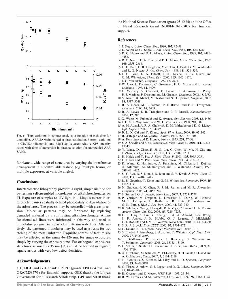
Fig. 6 Top: variation in contact angle as a function of etch time for
unmodified APA SAMs immersed in piranha solution. Bottom: variation
in C1s/Ti2p (diamonds) and P2p/Ti2p (squares) relative XPS intensity
ratios with time of immersion in piranha solution for unmodified APA
SAMs.
fabricate a wide range of structures by varying the interference
arrangement in a controllable fashion (e.g. multiple beams, or
multiple exposures, at variable angles).
Conclusions
Interferometric lithography provides a rapid, simple method for
patterning self-assembled monolayers of alkylphosphonates on
Ti. Exposure of samples to UV light in a Lloyd’s mirror inter-
ferometer causes spatially defined photocatalytic degradation of
the adsorbates. The process may be controlled with great preci-
sion. Molecular patterns may be fabricated by replacing
degraded material by a contrasting alkylphosphonate. Amine
functionalised lines were fabricated in this way and used to
immobilise polymer nanoparticles in 46 nm wide lines. Alterna-
tively, the patterned monolayer may be used as a resist for wet
etching of the metal substrate. Exquisite control of feature size
may be affected in the range 46–126 nm, for single exposures,
simply by varying the exposure time. For orthogonal exposures,
structures as small as 35 nm (l/7) could be formed in regular,
square arrays with very low defect densities.
Acknowledgements
GT, DGL and GJL thank EPSRC (grants EP/D064767/1 and
GR/C523857/1) for financial support. OEZ thanks the Libyan
Government for a Research Scholarship. GPL and SRJB thank
This journal is ª The Royal Society of Chemistry 2011
the National Science Foundation (grant 0515684) and the Office
of Naval Research (grant N00014-10-1-0907) for financial
support.
References
1 J. Sagiv, J. Am. Chem. Soc., 1980, 102, 92–98.2 L. Netzer and J. Sagiv, J. Am. Chem. Soc., 1983, 105, 674–676.3 R. G. Nuzzo and D. L. Allara, J. Am. Chem. Soc., 1983, 105, 4481–
4483.4 R. G. Nuzzo, F. A. Fusco and D. L. Allara, J. Am. Chem. Soc., 1987,
109, 2358–2368.5 C. D. Bain, E. B. Troughton, Y.-T. Tao, J. Evall, G. M. Whitesides
and R. G. Nuzzo, J. Am. Chem. Soc., 1989, 111, 321–335.6 J. C. Love, L. A. Estroff, J. K. Kriebel, R. G. Nuzzo and
G. M. Whitesides, Chem. Rev., 2005, 105, 1103–1170.7 J. G. van Alsten, Langmuir, 1999, 15, 7605.8 W. Gao, L. Dickinson, C. Grozinger, F. G. Morin and L. Reven,
Langmuir, 1996, 12, 6429.9 C. Viornery, Y. Chevolot, D. Leonar, B. Aronsson, P. Pechy,
H. J. Mathieu, P. Descouts and M. Graetzel, Langmuir, 2002, 18, 2582.10 S. Tosatti, R. Michel, M. Textor and N. D. Spencer, Langmuir, 2002,
18, 3537–3548.11 R. A. Neves, M. E. Salmon, P. E. Russell and E. B. Troughton,
Langmuir, 2000, 16, 2409.12 R. A. Neves, E. B. Troughton and P. E. Russell, Nanotechnology,
2001, 12, 285.13 X. Wang, M. Fujimaki and K. Awazu, Opt. Express, 2005, 13, 1486.14 J. E. G. J. Wijnhoven and W. L. Vos, Science, 1998, 281, 802.15 A. M. Adawi, A. R. A. Chalcraft, D. M. Whittaker and D. G. Lidzey,
Opt. Express, 2007, 15, 14299.16 B. Li, X. Cai and Y. Zhang, Appl. Phys. Lett., 2006, 89, 031103.17 B. O’Regan and M. Gratzel, Nature, 1991, 353, 737–740.18 A. Fujishima and K. Honda, Nature, 1975, 238, 37–38.19 S. A. Shevlin and S. M. Woodley, J. Phys. Chem. C, 2010, 114, 17333–
17343.20 Y. Wang, D. Zhao, H. Ji, G. Liu, C. Chen, W. Ma, H. Zhu and
J. Zhao, J. Phys. Chem. C, 2010, 114, 17728–17733.21 H. Haick and Y. Paz, J. Phys. Chem. B, 2001, 105, 3045–3054.22 H. Haick and Y. Paz, Chem. Phys. Chem., 2003, 4, 617–620.23 R. Wang, K. Hashimoto, A. Fujishima, M. Chikuni, E. Kojima,
A. Kitamura, M. Shimohigoshi and T. Watanabe, Nature, 1997,388, 431–432.
24 S.-Y. Ryu, D. S. Kim, J.-D. Jeon and S.-Y. Kwak, J. Phys. Chem. C,2010, 114, 17440–17445.
25 L. B. Goetting, T. Deng and G. M. Whitesides, Langmuir, 1999, 15,1182–1191.
26 N. Gadegaard, X. Chen, F. J. M. Rutten and M. R. Alexander,Langmuir, 2008, 24, 2057–2063.
27 S. Sun and G. J. Leggett, Nano Lett., 2007, 7, 3753–3758.28 P. Vettiger, M. Despont, U. Drechsler, U. Durig, W. Haberle,
M. I. Lutwyche, H. Rothuizen, R. Stuts, R. Widmer andG. K. Binnig, IBM J. Res. Dev., 2000, 44, 323–340.
29 K. Salaita, Y. Wang, J. Fragala, R. A. Vega, C. Liu and C. A. Mirkin,Angew. Chem., Int. Ed., 2006, 45, 7220–7223.
30 E. u. Haq, Z. Liu, Y. Zhang, S. A. A. Ahmad, L.-S. Wong,S. P. Armes, J. K. Hobbs, G. J. Leggett, J. Micklefield,C. J. Roberts and J. M. R. Weaver, Nano Lett., 2010, 10, 4375–4380.
31 S. R. J. Brueck, Proc. IEEE, 2005, 93, 1704–1721.32 C. Lu and R. H. Lipson, Laser Photonics Rev., 2009, 1–13.33 S. Friebel, J. Aizenberg, S. Abad and P. Wiltzius, Appl. Phys. Lett.,
2000, 77, 2406–2408.34 T. Geldhauser, P. Leiderer, J. Boneberg, S. Walheim and
T. Schimmel, Langmuir, 2008, 24, 13155–13160.35 C. Schuh, S. Santer, O. Prucker and J. Ruhe, Adv. Mater., 2009, 21,
4706–4710.36 A. Turchanin, M. Schnietz, M. El-Desawy, H. H. Solak, C. David and
A. Golzhauser, Small, 2007, 3, 2114–2119.37 N. Blondiaux, S. Zurcher, M. Liley and N. D. Spencer, Langmuir,
2007, 23, 3489–3494.38 G. Tizazu, A. Adawi, G. J. Leggett and D. G. Lidzey, Langmuir, 2009,
25, 10746–10753.39 R. Overney and E. Meyer, MRS Bull., 1993, 26–34.40 R. W. Carpick and M. Salmeron, Chem. Rev., 1997, 97, 1163–1194.
Nanoscale, 2011, 3, 2511–2516 | 2515

41 E. Gnecco, R. Bennewitz, T. Gyalog and E. Meyer, J. Phys.: Condens.Matter, 2001, 13, R619.
42 G. J. Leggett, N. J. Brewer and K. C. Chong, Phys. Chem. Chem.Phys., 2005, 7, 1107–1120.
43 L. Novotny and B. Hecht, Nanophotonics, Cambridge UniversityPress, Cambridge, UK, 2005.
2516 | Nanoscale, 2011, 3, 2511–2516
44 M. A. Sillanpaa and P. J. Hakonen, Physica E, 2002, 14, 41–47.
45 C. J. Boxley, H. S. White, C. E. Gardner and J. V. Macpherson,J. Phys. Chem. B, 2003, 107, 9677–9680.
46 J. N. Anker, W. P. Hall, O. Lyandres, N. C. Shah, J. Zhao andR. P. Van Duyne, Nat. Mater., 2008, 7, 442–453.
This journal is ª The Royal Society of Chemistry 2011
Copyright © 2022 FDOKUMEN