
Bioimprinted polymer platforms for cell culture using soft lithography
X-Ray Lithography-An Overview MARTIN C. PECKERAR, SENIOR MEMBER, IEEE, AND JUAN R. MALDONADO, MEMBER, IEEE
The fundamentals of X-ray lithography are reviewed. Issues associated with resolution, wafer throughput, and process lat- itude are discussed. X-ray lithography is compared with other lithographic technologies; future advancements, such as X-ray projection lithography, are described. It is shown that the ma- jor barrier to the near-term success of X-ray lithography is the requirement for a defect-fvee one-to-one mask which satisfies the stringent image-placement needs of submicrometer patterning.
I. INTRODUCTION No subject engenders more violent debate among mi-
croelectronics process engineers than future directions in lithographic technology. There is good reason for this. In terms of cost and time, microlithography is the most expensive and time-consuming of all unit processes in the microfabrication tool box [I]. Most circuit design rules are strongly influenced by lithographic tolerances and a dominant factor determining density of integration is the lithographic tool employed. The requirements placed on these tools for successful performance are technologically daunting. Companies rise and fall based on their ability to perform in this arena.
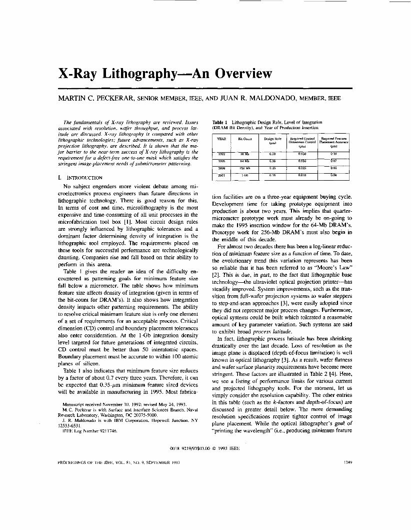
Table 1 gives the reader an idea of the difficulty en- countered as patteming goals for minimum feature size fall below a micrometer. The table shows how minimum feature size affects density of integration (given in terms of the bit-count for DRAM’s). It also shows how integration density impacts other patteming requirements. The ability to resolve critical minimum feature size is only one element of a set of requirements for an acceptable process. Critical dimension (CD) control and boundary placement tolerances also enter consideration. At the 1-Gb integration density level targeted for future generations of integrated circuits, CD control must be better than 50 interatomic spaces. Boundary placement must be accurate to within 100 atomic planes of silicon.
Table 1 also indicates that minimum feature size reduces by a factor of about 0.7 every three years. Therefore, it can be expected that 0.35-pm minimum feature sized devices will be available in manufacturing in 1995. Most fabrica-
Manuscript received November 10, 1992; revised May 24, 1993. M.C. Peckerar is with Surface and Interface Sciences Branch, Naval
J. R. Maldonado is with IBM Corporation, Hopewell Junction, NY
IEEE Log Number 92 1 1746.
Research Laboratory, Washington, DC 20375-5000.
12533-653 1.
Table 1 (DRAM Bit Density), and Year of Production Insertion
Lithographic Design Rule, Level of Integration
64 Mb 0.035
1998 256 Mb 0.25 0.025 0.05
2001 1 Gb 0.18
tion facilities are on a three-year equipment buying cycle. Development time for taking prototype equipment into production is about two years. This implies that quarter- micrometer prototype work must already be on-going to make the 1995 insertion window for the 64-Mb DRAM’s. Prototype work for 256-Mb DRAM’s must also begin in the middle of this decade.
For almost two decades there has been a log-linear reduc- tion of minimum feature size as a function of time. To date, the evolutionary trend this variation represents has been so reliable that it has been referred to as “Moore’s Law” [2]. This is due, in part, to the fact that lithographic base technology-the ultraviolet optical projection printer-has steadily improved. System improvements, such as the tran- sition from full-wafer projection systems to wafer steppers to step-and-scan approaches [3], were easily adopted since they did not represent major process changes. Furthermore, optical systems could be built which tolerated a reasonable amount of key parameter variation. Such systems are said to exhibit broad process latitude. In fact, lithographic process latitude has been shrinking
drastically over the last decade. Loss of resolution as the image plane is displaced (depth-of-focus limitation) is well known in optical lithography [3]. As a result, wafer flatness and wafer surface planarity requirements have become more stringent. These factors are illustrated in Table 2 [4]. Here, we see a listing of performance limits for various current and projected lithography tools. For the moment, let us simply consider the resolution capability. The other entries in this table (such as the k-factors and depth-of-focus) are discussed in greater detail below. The more demanding resolution specifications require tighter control of image plane placement. While the optical lithographer’s goal of “printing the wavelength” (i.e., producing minimum feature
00 18-92 19/93$03.OO 0 1993 IEEE
PROCEEDINGS OF THE IEEE, VOL. 81. NO. 9, SEPTEMBER 1993 I249
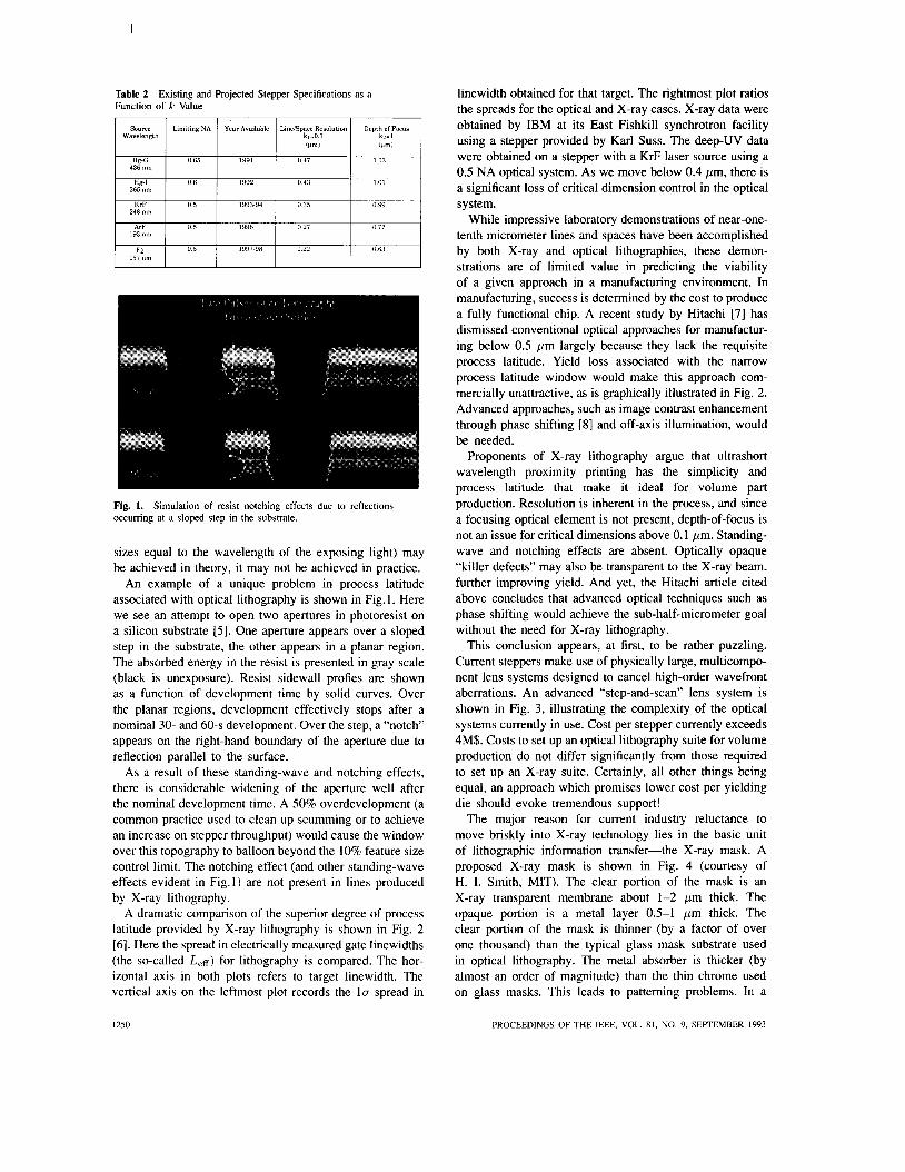
Table 2 Existing and Projected Stepper Specifications as a Function of k Value
Fig. 1. occurring at a sloped step in the substrate.
Simulation of resist notching effects due to reflections
sizes equal to the wavelength of the exposing light) may be achieved in theory, it may not be achieved in practice.
An example of a unique problem in process latitude associated with optical lithography is shown in Fig. 1. Here we see an attempt to open two apertures in photoresist on a silicon substrate [5] . One aperture appears over a sloped step in the substrate, the other appears in a planar region. The absorbed energy in the resist is presented in gray scale (black is unexposure). Resist sidewall profies are shown as a function of development time by solid curves. Over the planar regions, development effectively stops after a nominal 30- and 60-s development. Over the step, a “notch” appears on the right-hand boundary of the aperture due to reflection parallel to the surface.
As a result of these standing-wave and notching effects, there is considerable widening of the aperture well after the nominal development time. A 50% overdevelopment (a common practice used to clean up scumming or to achieve an increase on stepper throughput) would cause the window over this topography to balloon beyond the 10% feature size control limit. The notching effect (and other standing-wave effects evident in Fig.1) are not present in lines produced by X-ray lithography.
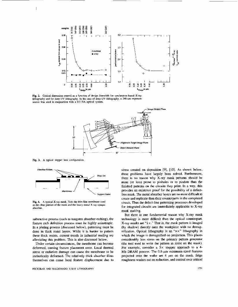
A dramatic comparison of the superior degree of process latitude provided by X-ray lithography is shown in Fig. 2 [6]. Here the spread in electrically measured gate linewidths (the so-called L,E) for lithography is compared. The hor- izontal axis in both plots refers to target linewidth. The vertical axis on the leftmost plot records the l a spread in
linewidth obtained for that target. The rightmost plot ratios the spreads for the optical and X-ray cases. X-ray data were obtained by IBM at its East Fishkill synchrotron facility using a stepper provided by Karl Suss. The deep-UV data were obtained on a stepper with a KrF laser source using a 0.5 NA optical system. As we move below 0.4 pm, there is a significant loss of critical dimension control in the optical system.
While impressive laboratory demonstrations of near-one- tenth micrometer lines and spaces have been accomplished by both X-ray and optical lithographies, these demon- strations are of limited value in predicting the viability of a given approach in a manufacturing environment. In manufacturing, success is determined by the cost to produce a fully functional chip. A recent study by Hitachi [7] has dismissed conventional optical approaches for manufactur- ing below 0.5 pm largely because they lack the requisite process latitude. Yield loss associated with the narrow process latitude window would make this approach com- mercially unattractive, as is graphically illustrated in Fig. 2. Advanced approaches, such as image contrast enhancement through phase shifting [8] and off-axis illumination, would be needed.
Proponents of X-ray lithography argue that ultrashort wavelength proximity printing has the simplicity and process latitude that make it ideal for volume part production. Resolution is inherent in the process, and since a focusing optical element is not present, depth-of-focus is not an issue for critical dimensions above 0.1 pm. Standing- wave and notching effects are absent. Optically opaque “killer defects” may also be transparent to the X-ray beam, further improving yield. And yet, the Hitachi article cited above concludes that advanced optical techniques such as phase shifting would achieve the sub-half-micrometer goal without the need for X-ray lithography.
This conclusion appears, at first, to be rather puzzling. Current steppers make use of physically large, multicompo- nent lens systems designed to cancel high-order wavefront aberrations. An advanced “step-and-scan’’ lens system is shown in Fig. 3, illustrating the complexity of the optical systems currently in use. Cost per stepper currently exceeds 4M$. Costs to set up an optical lithography suite for volume production do not differ significantly from those required to set up an X-ray suite. Certainly, all other things being equal, an approach which promises lower cost per yielding die should evoke tremendous support!
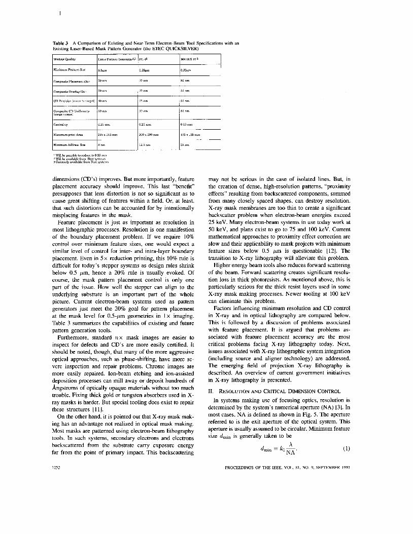
The major reason for current industry reluctance to move briskly into X-ray technology lies in the basic unit of lithographic information transfer-the X-ray mask. A proposed X-ray mask is shown in Fig. 4 (courtesy of H. I. Smith, MIT). The clear portion of the mask is an X-ray transparent membrane about 1-2 pm thick. The opaque portion is a metal layer 0.5-1 pm thick. The clear portion of the mask is thinner (by a factor of over one thousand) than the typical glass mask substrate used in optical lithography. The metal absorber is thicker (by almost an order of magnitude) than the thin chrome used on glass masks. This leads to patteming problems. In a
I250 PROCEEDINGS OF THE IEEE, VOL. 81, NO. 9, SEPTEMBER 1993
samples
8
0.02 0.013
I l
0 examer e x-ray \ L
I I I I I I I I I I
0 i Ld&e’” Ldesig““ P’
Fig. 2. Critical dimension control as a function of design linewidth for synchrotron-based X-ray lithography and for deep-UV lithography. In the case of deep-UV lithography, a 248-nm exposure source was used in conjunction with a 0.5 NA optical system.
,- Image (Wafer) Plane
Alignment Target Image Plane
Object (Reticle) Plane
Fig. 3. A typical stepper lens configuration.
Absorber Pattern
Membrane f 7 Support frame
Fig. 4. A typical X-ray mask. Note the thin-film membrane used as the clear portion of the mask and the heavy metal X-ray opaque absorber.
subtractive process (such as tungsten absorber etching), the feature etch definition process must be highly anisotropic. In a plating process (discussed below), patteming must be done in thick resist layers. While it is harder to pattern these thick resists, current trends in industrial tooling are alleviating this problem. This is also discussed below.
Under certain circumstances, the membrane can become deformed, causing feature placement error. Local thermal stress or radiation damage can cause the membrane to be inelastically deformed. The relatively thick absorber films themselves can cause local feature displacement due to
stress created on deposition [9], [lo]. As shown below, these problems have largely been solved. Furthermore, there is no reason why X-ray mask patterns should be more (or less) prone to pinholes or to pindots than the finished patterns on the circuits they print. In a way, this provides an existence proof for the possibility of a defect- free mask. The metal absorber layers are no more difficult to create and replicate than their counterparts in the completed circuit. Thus the defect-free patterning processes developed for integrated circuits are immediately applicable to X-ray mask making.
But there is one fundamental reason why X-ray mask technology is more difficult than the optical counterpart. X-ray masks are “1 x.” That is, the mask pattern is imaged (by shadow) directly onto the workpiece with no demag- nification. Optical lithography is an “ n x ” lithography in which the image is demagnified on projection. This places considerably less stress on the primary pattem generator (the tool used to write the pattem in resist on the mask). For example, consider a 5x stepper approach to a 4- Mb DRAM process. The 0.8-pm minimum-sized features projected onto the wafer are 4 pm on the mask. Edge roughness washes out on reduction, and control over critical
PECKERAR AND MALDONADO: X-RAY LITHOGRAPHY 1251
Wntlng Quality L~~~~ pattern ~ ~ ~ ~ ~ ~ t a ~ 1 . 3
Minrmum Feature Size 0 5pm
ELQ MEBES IV 3 I
0 25pm 0 35pm
I Minimum Address Size 18 nm I 12.5 nm 12.5 nm
Composite Placement (301
Composite overlay (30)
CD Precisian (mean to target)
Composite CD Uniformity (mean to mad
Centrality
Maximum pnnt Area
1 Will be possible ta reduce to 0.35 mm Will be available from Eke systems
3 Currently available h.om Etec systems
30 mm 30 nm 80 nm
30 nm 30 nm 50 nm
40 nm 25 nm 50 nm
60 nm 30 nm 50 nm
0 25 mm 0 25 mm 0 15 mm
215 x 215 mm 200 x 200 mm 155 x 155 mm
dimensions (CD’s) improves. But more importantly, feature placement accuracy should improve. This last “benefit” presupposes that lens distortion is not so significant as to cause great shifting of features within a field. Or, at least, that such distortions can be accounted for by intentionally misplacing features in the mask.
Feature placement is just as important as resolution in most lithographic processes. Resolution is one manifestion of the boundary placement problem. If we require 10% control over minimum feature sizes, one would expect a similar level of control for inter- and intra-layer boundary placement. Even in 5 x reduction printing, this 10% rule is difficult for today’s stepper systems as design rules shr ink below 0.5 pm, hence a 20% rule is usually evoked. Of course, the mask pattem placement control is only one part of the issue. How well the stepper can align to the underlying substrate is an important part of the whole picture. Current electron-beam systems used as pattem generators just meet the 20% goal for pattem placement at the mask level for 0.5-pm geometries in l x imaging. Table 3 summarizes the capabilities of existing and future pattem generation tools.
Furthermore, standard n x mask images are easier to inspect for defects and CD’s are more easily certified. It should be noted, though, that many of the more aggressive optical approaches, such as phase-shifting, have more se- vere inspection and repair problems. Chrome images are more easily repaired. Ion-beam etching and ion-assisted deposition processes can mill away or deposit hundreds of Angstroms of optically opaque materials without too much trouble. Fixing thick gold or tungsten absorbers used in X- ray masks is harder. But special tooling does exist to repair these structures [ 111.
On the other hand, it is pointed out that X-ray mask mak- ing has an advantage not realized in optical mask making. Most masks are pattemed using electron-beam lithography tools. In such systems, secondary electrons and electrons backscattered from the substrate carry exposure energy far from the point of primary impact. This backscattering
may not be serious in the case of isolated lines. But, in the creation of dense, high-resolution pattems, “proximity effects” resulting from backscattered components, summed from many closely spaced shapes, can destroy resolution. X-ray mask membranes are too thin to create a significant backscatter problem when electron-beam energies exceed 25 keV. Many electron-beam systems in use today work at 50 keV, and plans exist to go to 75 and 100 keV. Current mathematical approaches to proximity effect correction are slow and their applicability to mask projects with minimum feature sizes below 0.5 pm is questionable [12]. The transition to X-ray lithography will alleviate this problem.
Higher energy beam tools also reduces forward scattering of the beam. Forward scattering creates significant resolu- tion loss in thick photoresists. As mentioned above, this is particularly serious for the thick resist layers used in some X-ray mask making processes. Newer tooling at 100 keV can eliminate this problem.
Factors influencing minimum resolution and CD control in X-ray and in optical lithography are compared below. This is followed by a discussion of problems associated with feature placement. It is argued that problems as- sociated with feature placement accuracy are the most critical problems facing X-ray lithography today. Next, issues associated with X-ray lithographic system integration (including source and aligner technology) are addressed. The emerging field of projection X-ray lithography is described. An overview of current govemment initiatives in X-ray lithography is presented.
11. RESOLUTION AND CRITICAL DIMENSION CONTROL In systems making use of focusing optics, resolution is
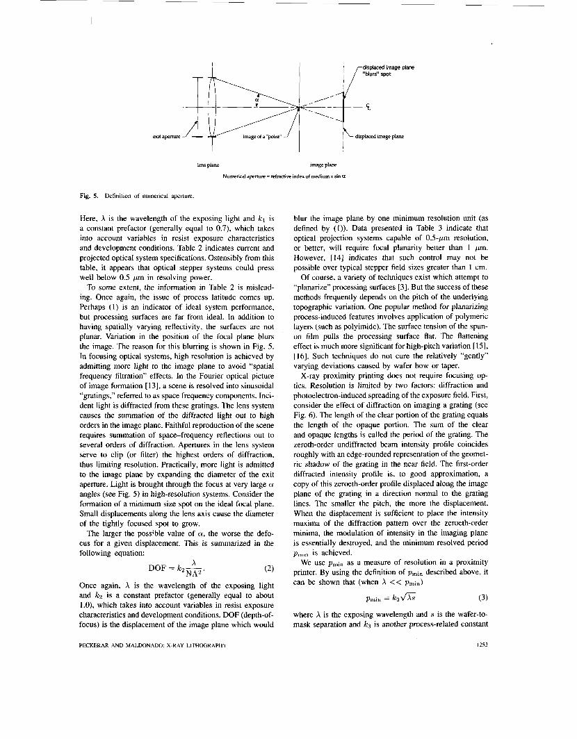
determined by the system’s numerical aperture (NA) [3]. In most cases, NA is defined as shown in Fig. 5. The aperture referred to is the exit aperture of the optical system. This aperture is usually assumed to be circular. Minimum feature size dmin is generally taken to be
A NA ’ (1) dmin = IC-
1252 PROCEEDINGS OF THE IEEE, VOL. 81, NO. 9. SEPTEMBER 1993
T P displaced image plane “blurs” spot
lens plane image plane
Numerical aperture = refractive index of medium x sin a
Fig. 5. Definition of numerical aperture.
Here, X is the wavelength of the exposing light and k1 is a constant prefactor (generally equal to 0.7), which takes into account variables in resist exposure characteristics and development conditions. Table 2 indicates current and projected optical system specifications. Ostensibly from this table, it appears that optical stepper systems could press well below 0.5 pm in resolving power.
To some extent, the information in Table 2 is mislead- ing. Once again, the issue of process latitude comes up. Perhaps ( 1 ) is an indicator of ideal system performance, but processing surfaces are far from ideal. In addition to having spatially varying reflectivity, the surfaces are not planar. Variation in the position of the focal plane blurs the image. The reason for this blurring is shown in Fig. 5. In focusing optical systems, high resolution is achieved by admitting more light to the image plane to avoid “spatial frequency filtration” effects. In the Fourier optical picture of image formation [ 131, a scene is resolved into sinusoidal “gratings,” referred to as space frequency components. Inci- dent light is diffracted from these gratings. The lens system causes the summation of the diffracted light out to high orders in the image plane. Faithful reproduction of the scene requires summation of space-frequency reflections out to several orders of diffraction. Apertures in the lens system serve to clip (or filter) the highest orders of diffraction, thus limiting resolution. Practically, more light is admitted to the image plane by expanding the diameter of the exit aperture. Light is brought through the focus at very large a angles (see Fig. 5) in high-resolution systems. Consider the formation of a minimum size spot on the ideal focal plane. Small displacements along the lens axis cause the diameter of the tightly focused spot to grow.
The larger the possible value of a, the worse the defo- cus for a given displacement. This is summarized in the following equation:
X NA
DOF = k p y .
Once again, X is the wavelength of the exposing light and l c p is a constant prefactor (generally equal to about l.O), which takes into account variables in resist exposure characteristics and development conditions. DOF (depth-of- focus) is the displacement of the image plane which would
blur the image plane by one minimum resolution unit (as defined by (1)). Data presented in Table 3 indicate that optical projection systems capable of 0.5-pm resolution, or better, will require focal planarity better than 1 /Am. However, [14] indicates that such control may not be possible over typical stepper field sizes greater than 1 cm.
Of course, a variety of techniques exist which attempt to “planarize” processing surfaces [ 3 ] . But the success of these methods frequently depends on the pitch of the underlying topographic variation. One popular method for planarizing process-induced features involves application of polymeric layers (such as polyimide). The surface tension of the spun- on film pulls the processing surface flat. The flattening effect is much more significant for high-pitch variation [ 151, [16]. Such techniques do not cure the relatively “gently” varying deviations caused by wafer bow or taper.
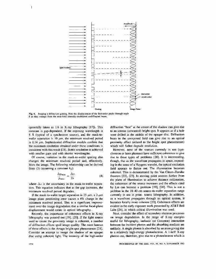
X-ray proximity printing does not require focusing op- tics. Resolution is limited by two factors: diffraction and photoelectron-induced spreading of the exposure field. First, consider the effect of diffraction on imaging a grating (see Fig. 6). The length of the clear portion of the grating equals the length of the opaque portion. The sum of the clear and opaque lengths is called the period of the grating. The zeroth-order undiffracted beam intensity profile coincides roughly with an edge-rounded representation of the geomet- ric shadow of the grating in the near field. The first-order diffracted intensity profile is, to good approximation, a copy of this zeroeth-order profile displaced along the image plane of the grating in a direction normal to the grating lines. The smaller the pitch, the more the displacement. When the displacement is sufficient to place the intensity maxima of the diffraction pattern over the zeroeth-order minima, the modulation of intensity in the imaging plane is essentially destroyed, and the minimum resolved period pmin is achieved.
We use pmin as a measure of resolution in a proximity printer. By using the definition of pmin described above, it can be shown that (when X << pmin)
pmin = k3& (3)
where X is the exposing wavelength and s is the wafer-to- mask separation and kg is another process-related constant
PECKERAR AND MALDONADO: X-RAY LITHOGRAPHY 1253
L Amplitude \I D
D
D
D
D
D
D
D
D
D
D
t
D
D
light incident
D
D
D
D
D
D
D
D
D P Grating H Image Plane
Fig. 6. Imaging a diffraction grating. Note the displacement of the first-order peaks through angle 0 as they emerge from the near-field intensity-modulated undiffracted beam.
(generally taken as 1.6 in X-ray lithography [17]). This constant is gap-dependent. If the exposing wavelength is 8 a (typical of a synchrotron source), and the mask-to- wafer separation is 10 pm, the minimum resolved period is 0.14 pm. Sophisticated diffraction models confirm that the minimum resolution obtained under these conditions is consistent with this result [ 181. Better resolution is achieved with smaller gaps and with shorter wavelengths.
Of course, variation in the mask-to-wafer spacing also changes the minimum resolved period and, effectively, blurs the image. The following relationship can be derived from (3) (assuming a constant k3):
(4)
where As is the uncertainty in the mask-to-wafer separa- tion. This equation indicates that as the gap increases, the minimum resolved period degrades.
If the mask-to-wafer target separation is 25 pm, a 2-pm image plane positioning error causes a 4% change in the minimum resolved period. This is a significant improve- ment over the image degradation that a similar focal-plane displacement would create in optical lithography.
Recently, the importance of coherence effects in X-ray lithography was pointed out [19], [20]. If the light source used to create the proximity image is coherent, a number of diffraction effects spoil image quality. The most famous of these effects is the Arrago bright-spot phenomenon [21]. Consider an attempt to image the shadow of an opaque disc using coherent light. The intensity of the high-order
diffraction “beat” at the center of the shadow can give rise to an intense (unwanted) bright spot. It appears as if a hole were drilled in the middle of the opaque disc. Diffraction beats in the unexposed field can give rise to an optical proximity effect (related to the bright spot phenomenon) which will futher degrade resolution.
However, none of the sources currently in use (syn- chrotron or laser plasmas) have sufficient coherence to give rise to these types of problems [20]. It is intereresting, though, that as the wavefront propagates in space, expand- ing in the sense of a Huygens wavelet, the optical excitation field appears to flatten out. The illumination becomes coherent. This is demonstrated by the Van Cittert-Zemike theorem [22], [23]. In moving point sources further from the plane of illumination to achieve distance collimation, the coherence of the source increases and the effects cited by Lin can become a problem [19], [20]. This is not a problem in the 10-40-cm source-to-wafer separation range currently in use in point- source lithography. In addition, as a wavefront propagates through an optical system, it becomes locally more coherent [23]. Coherence effects are evident in the early exposure work presented by AT&T Bell Labs [24], in which critical illumination was used.
Next, consider the effect of secondary electron processes on image degradation. In the range of X-ray energies useful for lithography, inelastic (or Compton) interaction between the incident photon and the absorbing medium are unlikely. A single photon is absorbed by an atom giving rise to a relatively high-energy photoelectron. A 1-keV X-ray photon can, therefore, give rise to a photoelectron which is
I254 PROCEEDINGS OF THE IEEE, VOL. S I , NO. 9, SEPTEMBER 1 9 3
near a kiloelectronvolt in energy. As a rule, for absorbing substrates with a density and composition similar to the photoresist, the photoelectron will travel 0.1 pm from its point of origin for every kilovolt of kinetic energy. This “rule-of-thumb” was confirmed for soft X-rays in a classic experiment by Feder et al. [25] Thus a 10-8, X-ray beam should produce exposure in the normally opaque region of a mask, under the feature by about 0.12 pm on a side. This massive undercutting effect can be avoided by proper resist development. However, in practice, some resolution has been achieved with X-ray contact printing.
The apparent inconsistency between experiments has recently been resolved by Early et al. [26], and by Ocola and Cerrina [27]. Feder’s experiment involved the use of erbium films deposited on photoresist and illuminated by a soft X-ray beam. The heavy metal produced many high-energy secondary electrons. The energy distribution of these photoelectrons was very narrow and close to the incident photon energy. Feder then measured the maximum extent of the resist damage as indicated by a change in resist dissolution rate. In actual resist exposures, the high-energy secondaries from the heavy metal absorber are absent. Also, early work in X-ray lithography was accomplished with tube sources containing a high-energy continuum component of radiation which is absent in current-day plasma or synchrotron sources. Even with this high-energy component present, it was possible to control resist exposure profile by optimizing development cycles for the resist [28].
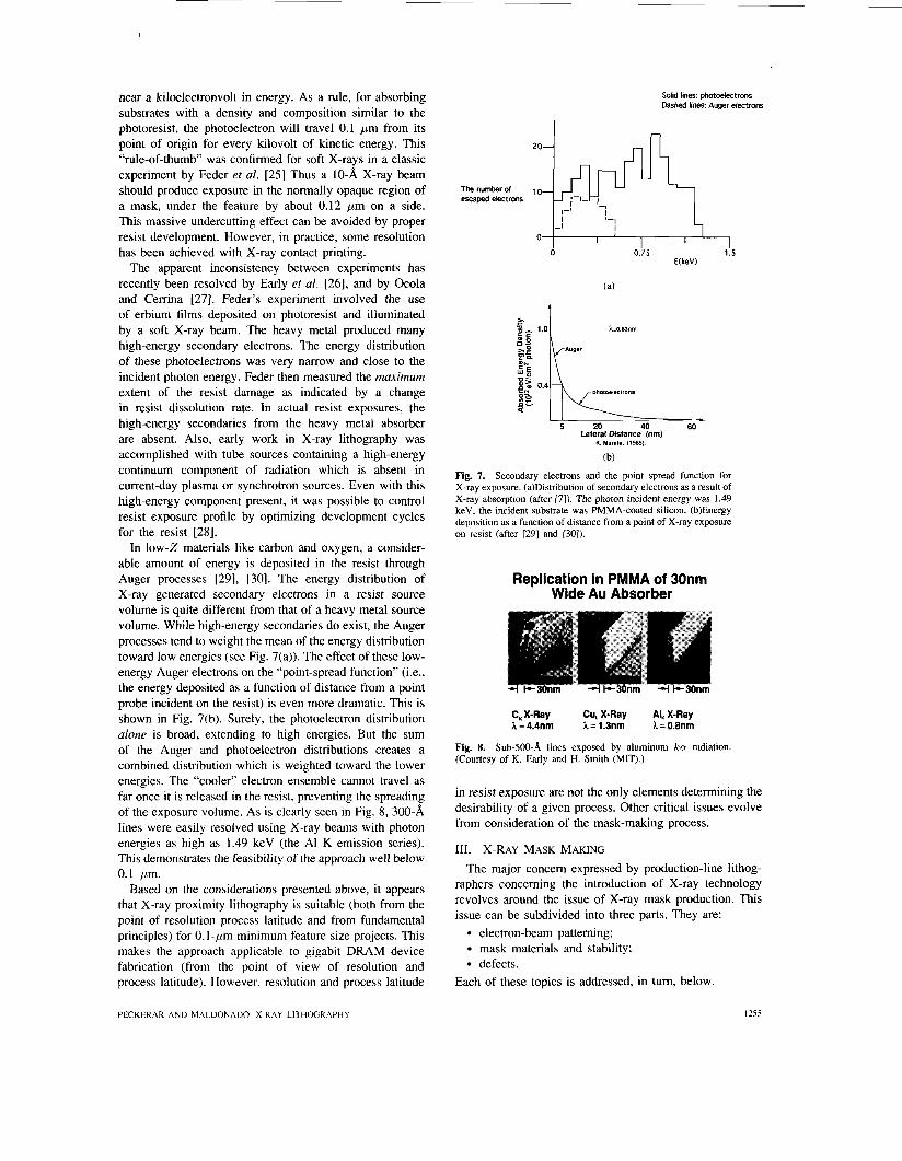
In low-2 materials like carbon and oxygen, a consider- able amount of energy is deposited in the resist through Auger processes [29], [30]. The energy distribution of X-ray generated secondary electrons in a resist source volume is quite different from that of a heavy metal source volume. While high-energy secondaries do exist, the Auger processes tend to weight the mean of the energy distribution toward low energies (see Fig. 7(a)). The effect of these low- energy Auger electrons on the “point-spread function” (i.e., the energy deposited as a function of distance from a point probe incident on the resist) is even more dramatic. This is shown in Fig. 7(b). Surely, the photoelectron distribution alone is broad, extending to high energies. But the sum of the Auger and photoelectron distributions creates a combined distribution which is weighted toward the lower energies. The “cooler” electron ensemble cannot travel as far once it is released in the resist, preventing the spreading of the exposure volume. As is clearly seen in Fig. 8, 300-8, lines were easily resolved using X-ray beams with photon energies as high as 1.49 keV (the AI K emission series). This demonstrates the feasibility of the approach well below 0.1 pm.
Based on the considerations presented above, it appears that X-ray proximity lithography is suitable (both from the point of resolution process latitude and from fundamental principles) for 0.1-pm minimum feature size projects. This makes the approach applicable to gigabit DRAM device fabrication (from the point of view of resolution and process latitude). However, resolution and process latitude
The number of escaped electrons
Solid lines: photoelectrons Dashed lines: Auger electrons
“d 0.75 1.5
E(keV)
t
pholoeleclrons 0‘4L 5 20 40 60
Lateral Distance (nm) U. Muram, (1985).
pholoeleclrons 0 . 4 h
5 20 40 60 Lateral Distance (nm)
U. Muram, (1985).
(b)
Fig. 7. Secondary electrons and the point spread function for X-ray exposure. (a)Distribution of secondary electrons as a result of X-ray absorption (after [7]). The photon incident energy was 1.49 keV, the incident substrate was PMMA-coated silicon. (b)Energy deposition as a function of distance from a point of X-ray exposure on resist (after [29] and [30]).
Replication in PMMA of 30nm Wide Au Absorber
C, X-Ray Cu, X-Ray AL X-Ray h=4.4nm h=1.3nm h=0.8nm
Fig. 8. (Courtesy of K. Early and H. Smith (MIT).)
Sub-500-A lines exposed by aluminum ka radiation
in resist exposure are not the only elements determining the desirability of a given process. Other critical issues evolve from consideration of the mask-making process.
111. X-RAY MASK MAKING The major concem expressed by production-line lithog-
raphers concerning the introduction of X-ray technology revolves around the issue of X-ray mask production. This issue can be subdivided into three parts. They are:
electron-beam patterning; mask materials and stability; defects.
Each of these topics is addressed, in tum, below.
PECKERAR AND MALDONADO: X-RAY LITHOGRAPHY 1255
f line spreading due to secondary and backscatter processes
incident Beam diameter # l-bxcel - to - excel spacing (address structure)
Fig. 9. Electron-beam exposing a line of photoresist.
A . Electron-Beam Patterning At the beginning of the last decade, a series of factors
appeared which lessened the demand for improved electron- beam mask-making tools. Prior to the 1980’s, the bulk of all mask making was 1 x in nature. Contact and proximity printers all made one-to-one reproductions of desired pat- terns. In the late 1970’s full wafer projection systems were introduced. These systems still made use of 1 x projectors. The next major development in wafer printing technology occurred with the introduction of the GCA 4800 wafer stepper. This tool projected a lox demagnified image onto the workpiece. Thus all of the critical specifications for the primary patterning tool-resolution, edge roughness, boundary placement accuracy, etc.- were relaxed by an order of magnitude.
The ability to inspect and to repair masks also improved for a number of reasons. First, the size of a “printable” defect on a mask was larger. Submicrometer defects on mask did not resolve on pattern transfer to the wafer. The larger, potentially more serious defects were easy to spot. Laser “zapping” and “plugging” operations were developed to eliminate these defects. One of the major sources of these defects is particles in the environment. By some estimates, the density of particles in a unit volume of air climbs as the inverse third power of the particle diameter. Thus there are fewer large particles than small ones to create the fatal damage sites.
Over time, chip sizes grew and the demands on optical stepper systems increased. Current demagnification factors are close to 5x. Even though demagnification is lower (by a factor of 2) than it was in the past, mask making specifications become more stringent on going to X-ray technology. The question remains, to what degree can electron-beam mask making technology respond to the needs of X-ray lithography?
First consider the issue of resolution. The ability of an electron beam to resolve isolated features depends on three factors-beam diameter, address structure, and the interaction of the beam with the material it is incident on. Due to their short effective wavelength, electron diffraction effects are not important. Electron-beam lithography tools with 80-A beam diameters are currently available commer- cially. Spot size is rarely a limiting factor in electron-beam resolution.
To understand address structure, we must have some understanding of how the electron beam exposes resist.
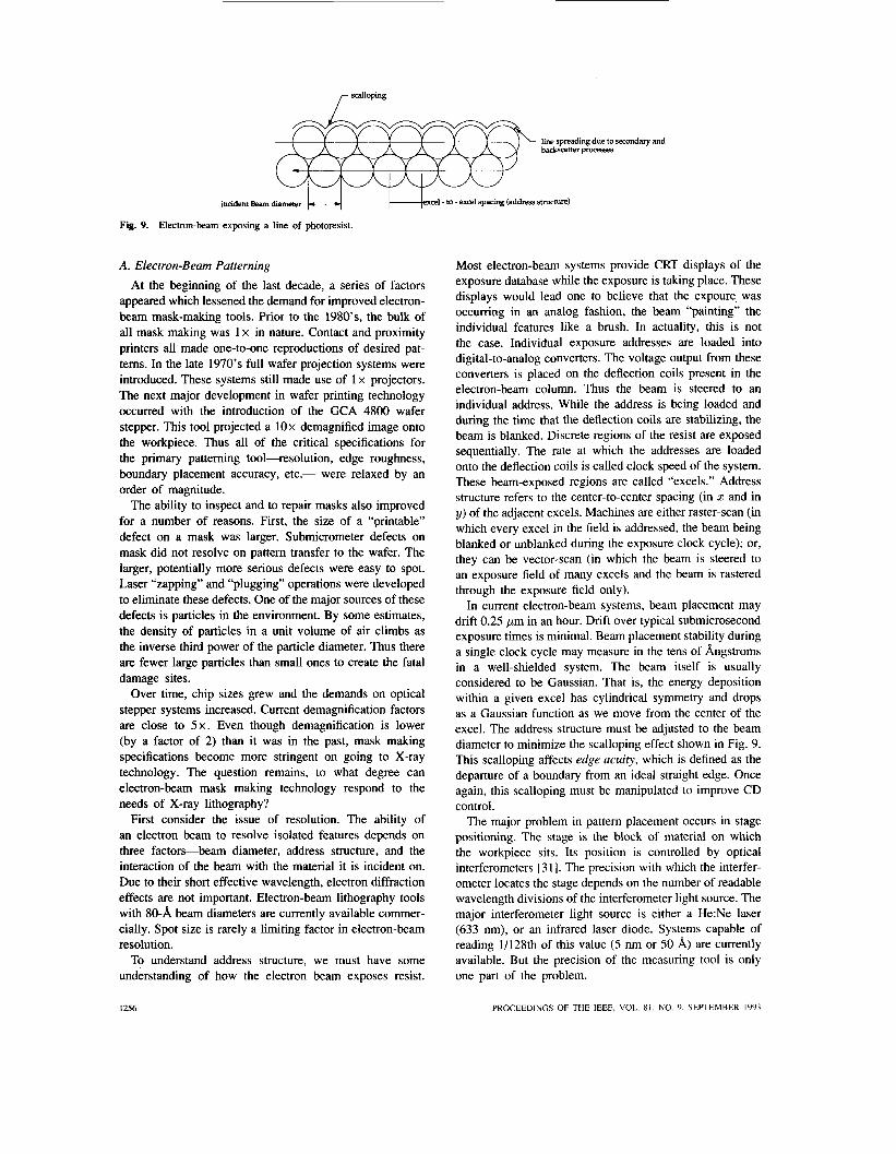
Most electron-beam systems provide CRT displays of the exposure database while the exposure is taking place. These displays would lead one to believe that the expoure, was occumng in an analog fashion, the beam “painting” the individual features like a brush. In actuality, this is not the case. Individual exposure addresses are loaded into digital-to-analog converters. The voltage output from these converters is placed on the deflection coils present in the electron-beam column. Thus the beam is steered to an individual address. While the address is being loaded and during the time that the deflection coils are stabilizing, the beam is blanked. Discrete regions of the resist are exposed sequentially. The rate at which the addresses are loaded onto the deflection coils is called clock speed of the system. These beam-exposed regions are called “excels.” Address structure refers to the center-to-center spacing (in z and in y) of the adjacent excels. Machines are either raster-scan (in which every excel in the field is addressed, the beam being blanked or unblanked during the exposure clock cycle); or, they can be vector-scan (in which the beam is steered to an exposure field of many excels and the beam is rastered through the exposure field only).
In current electron-beam systems, beam placement may drift 0.25 pm in an hour. Drift over typical submicrosecond exposure times is minimal. Beam placement stability during a single clock cycle may measure in the tens of Angstroms in a well-shielded system. The beam itself is usually considered to be Gaussian. That is, the energy deposition within a given excel has cylindrical symmetry and drops as a Gaussian function as we move from the center of the excel. The address structure must be adjusted to the beam diameter to minimize the scalloping effect shown in Fig. 9. This scalloping affects edge acuity, which is defined as the departure of a boundary from an ideal straight edge. Once again, this scalloping must be manipulated to improve CD control.
The major problem in pattem placement occurs in stage positioning. The stage is the block of material on which the workpiece sits. Its position is controlled by optical interferometers [3 11. The precision with which the interfer- ometer locates the stage depends on the number of readable wavelength divisions of the interferometer light source. The major interferometer light source is either a He:Ne laser (633 nm), or an infrared laser diode. Systems capable of reading 1/128th of this value (5 nm or 50 A) are currently available. But the precision of the measuring tool is only one part of the problem.
1256 PROCEEDINGS OF THE IEEE. VOL. 81, NO. 9, SEITEMBER 1993
If one is interested in pattem placement at the level of tens of atomic planes, the natural movements of what appear to be solid materials must be taken into account. At the 100-A level, the stage appears to be more like jello than metal. The system’s mechanical viabration and thermal distortions must be minimized. Temperatures must be controlled to a fraction of a degree and dynamic me- chanical models of the system must be constructed to avoid resonances. Also, column contamination can lead to charging and spurious beam deflection.
The fact that electron beams are generated in vacuum causes further difficulty. For mechanical systems operating in air, it is possible to move masses using an “air bearing.” This is simply a surface pierced with air jets. These jets suspend the mass above the fixed surface and allow the mass to be moved without the vibrations of roller bear- ings. Obviously, this is not possible in a vacuum. Newer approaches, such as those proposed by IBM, involve stages sliding on optically polished surfaces. Gravity constrains the stage to a well-defined plane, thus eliminating pitch- and yaw-type motions. The stage can be pushed in x, y and 8 by bars. An overview of current and projected electron-beam capabilities is given in Table 3.
It should also be pointed out that alternate approaches to mask making are also possible. Pattem generators which use laser beams in place of electrons are currently in use. Pattern positioning is excellent with these tools. But resolution is a problem, as is indicated in Table 3. In some cases, the “daughter mask” approach is valid. Here, an optical projection stepper with exceptionally high NA is used to print the X-ray mask from a reticle. The reticle is nx larger than the printed image, and the positioning error scales with the demagnification. Lens distortions could be corrected in the reticle for each tool used. Resolution is good since the X-ray mask surface receiving the projection print is ideally flat and of controlled reflectivity. The full potential of this approach is only now being explored. Of course, ultimate resolution would not be as good as a high-resolution electron-beam print.
In the following section, we move on to study the material configurations used to create an X-ray mask.
Be 25 150
B. Mask Materials In this section, we cover the fundamentals necessary to
understand the various materials choices that are made to create an effective X-ray mask technology. In addition to issues relating to long-term stability and pattern placement accuracy, we also address mask defect and damage prob- lems. We conclude the discussion with a description of potential X-ray irradiation damage to the mask materials. As the incident radiation can also influence the performance of the devices fabricated, this possibility is also discussed.
The power of an X-ray beam is rapidly dissipated as it propagates into solid matter. Different materials have widely varying X-ray absorption powers. But as a rule, elements of lighter atomic weight will transmit X-rays farther. X-ray absorption can be computed easily from
123 Unknown ,027 1 4 7 Bad 39
Table 4 A Comparison of Various Mask Substrate Material Candidates
Beers Law
where I ( t ) is the intensity of the incident beam transmitted to a thickness t , IO is the incident intensity, p is the mass absorption coefficient of the transmitting medium, and p is the density of the medium. Mass aborption coefficients have been tabulated for all elements and are readily available [32]. As a rule-of-thumb, transmission should be better than 50%. Many solids can be formed as membranes of thicknesses in the 1-2-pm range. Silicon, silicon carbide, and diamond membranes are currently under active study as candidates for production mask substrates. In the United States, silicon membranes are the most widely used. A com- parison of relevant properties of these various membranes is shown in Table 4.
In this table, key rating factors include the X-ray trans- missivity (as reflected in the t 5 0 ~ value), thermal conduc- tivity, thermal expansion coefficient, the susceptibility of the membrane to radiation damage, the membrane strength, its elasticity, and the optical transparency. It is important that the membrane be thermally conductive, as it will heat during exposure. Thermal displacement effects can be mitigated somewhat if the material has a low coef- ficient of thermal expansion. But the overall expansion of the total mask structure should match the wafer to be printed. It is important that the films be optically transparent. Most current or projected alignment systems make use of through-the-membrane optical imaging. A relative unweighted figure of merit could be defined by simply multiplying the the numerical value of each of these factors and dividing the result by the figure obtained for a silicon membrane. Thus silicon is used as a de facro standard in the study.
PECKERAR AND MALDONADO X-RAY LITHOGRAPHY 1257
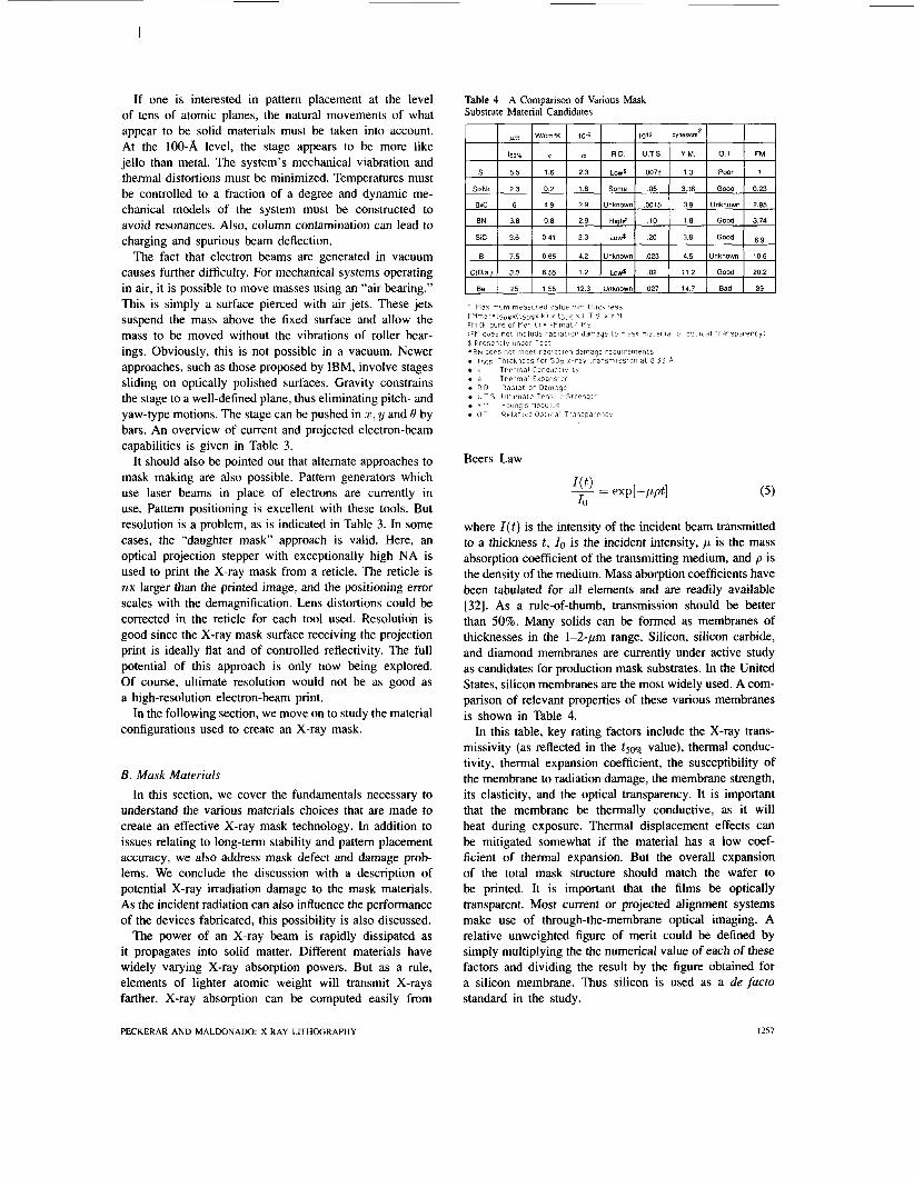
Phntnresist Thin Gold Dhoto base
Pattemed Photoresist
gold plating bath v- Fig. 10. A schematic of the up-plating process for X-ray masks.
From the table, it would appear that beryllium is an exceptionally good choice. But this figure is unrealistically high, as it does not include the zero optical transmissivity. It is possible to create “outboard” alignment marks of another material outside of the marks. In this case, beryllium would be an excellent mask material, under the standards of this study. But these outboard marks are troublesome and require special aligner configurations. The same is true for boron. Also, the properties of boron and carbon tetraboride membranes are unknown. For many years BN films were the standard mask making materials. But the poor radiation response of these membranes has made them impractical for everyday use. Diamond and silicon carbide appear to be somewhat better than silicon and both are under active development as X-ray membranes. Issues of uniformity of thickness, surface roughness, optical and X- ray transmissivities currently prevent deployment. There are a number of programs vigorously trying to get suitable membranes in these materials.
Heavy metal absorbers are used to create the opaque re- gions of the mask. In the past, the gold up-plating technique was the most widely practiced absorber technology. This process is illustrated in Fig. 10. A thin (5 1000 8, ) gold plating base is applied to the silicon membrane. This base serves as the electrical contact to the plating solution. Resist is spun over the base and pattemed in such a way as to leave slots where the absorber will be placed. The plate is immersed in a plating bath and the desired thickness of gold is deposited. Resist is stripped and the mask is complete. A typical X-ray mask structure is shown in Fig. 4.
It was formerly thought that the absorber must be less
Resiststrip
Dipped to remove thin plating base
than 10% transmissive. This would lead to better than a 10: 1 transmissivity ratio between the clear and opaque regions. A gold film 3000 8, thick would provide this transmissivity for incident beams whose photon energy is typical of point- source lithography ( about 1 keV). While standard chrome photoplates used in optical lithography have contrast ratios this high, by the time the light passes through the interven- ing optics, contrast ratios rarely exceed 3: 1. Lower contrast ratios and thinner absorbers in X-ray masks are clearly tolerable. Synchrotron applications currently in use call for absorber thicknesses in the 4000-7000-8, range (due to higher energies of incidence). Thinner absorbers are easier to pattem. A partially transmissive membrane can actually be constructed which would create better contrast than a thicker one. There is a phase shift due to index differences on transmission through the clear and “opaque” portions of the mask. If phases in the clear and opaque regions differ by 180°, there will be an enhancement of contrast at the boundary, just as in optical phase shifting [20].
Gold is a very “forgiving” material when it is used as an absorber. It is fairly compliant, and stress mismatch betweeen it and the underlying silicon will not lead to deformation of the pattem during the plating process. But plating does have its drawbacks. It is a multistep process involving the deposition of a base layer as well as the up- plated metal. Grain structure and residual stress are strong functions of bath temperature and concentration and are somewhat difficult to control. Current trends in integrated circuit fabrication favor subtractive etching processes for low defect film production. Gold, though, is very difficult to etch anisotropically. Other absorbers must be sought to accomplish this task.
1258 PROCEEDINGS OF THE IEEE, VOL. 81, NO. 9, SEPTEMBER 1993
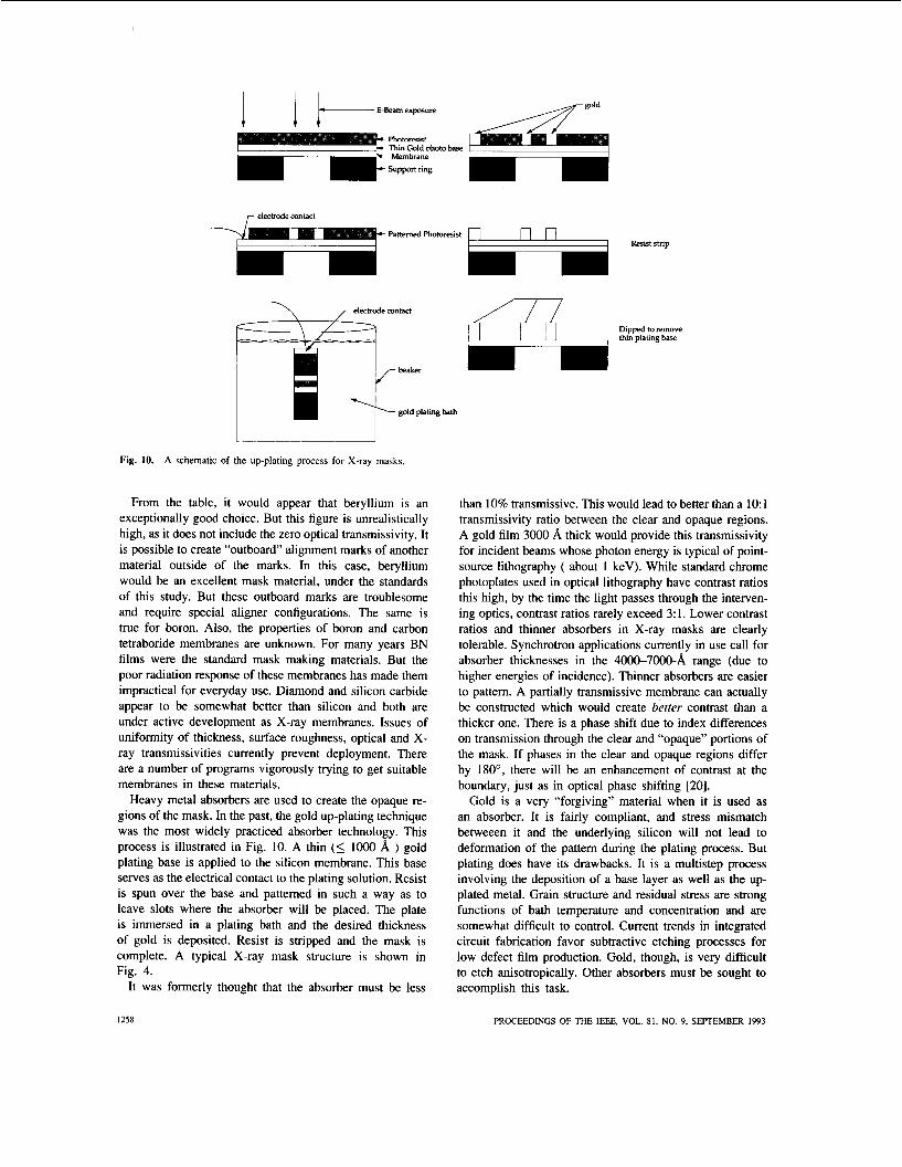
Fig. 11. Stress distribution in a mounted membrane created by heating in the synchrotron. The support ring has an outer diameter of 120 mm and an inner diameter of 82 mm. The ring thickness is 7 nun. The maximum in-plane distortion resulting from the exposure was less than 20 8, . (Courtesy of Prof. R.. Engelstadt.)
Tungsten is an absorber material of considerable promise. It is strongly absorptive and possible to pattem by anisotropic plasma etch processes [33]. Stress mismatch is a problem which has been overcome in a variety of laboratories [34]. Generally, tungsten is sputtered in an inert gas ambient. Varying the background pressure leads to changes in stress in the deposited film. The deposited film stress can vary from compressive to tensile, depending on background ambient pressure of the inert gas. Membrane stress can be measured during the deposition process by driving the membrane into resonance acoustically (as though it were a microphone). The resonant frequency in vacuum depends on membrane stress and on tabulated physical constants of the material. Thus measuring the resonance peak determines film stress. The Massachussetts Institute of Technology group [34] has developed a closed- loop system exercising real-time control of background pressure, and they have produced stress-free films with it.
The problem of absorber stress can be modeled numer- ically. The film can be viewed as a lattice of springs (either in tension or in compression) anchored to the membrane surface. Thermal and mechanical stress mod- eling approaches exist [35] which provide indications of the local stress pattems before and after patterning. The resulting feature displacements can be computed from these models. Highly accurate finite-element codes can com- pute the amount of membrane distortion occuring during mounting in a stepper system or due to local heating of the membrane during X-ray exposure. An example of this modeling [36] (courtesy of Dr. R. Engelstadt, University of Wisconsin-Madison), is shown as Fig 11. The red line in the center of the mask disk represents the region of largest thermally induced mask distortion. The changing colors indicate reduced distortion as we move away from the region of beam exposure. Despite the brilliant color contrast appearing in this image, thermal distortions are on the order of nanometers. For all of the absorber/membrane systems described above, patteming-induced distortion, mounting stresses or thermal stresses do not appear to be major issues.
There is one distortion-related issue which has not been settled as of this writing. That is the issue relating to radiation-induced mask damage. Let us assume, for a moment that we are exposing a 1-cm2 field on a mask every second. Incident dose required to expose most X- ray photoresists is about 100 mJ/cm2. Assume 10% of this is absorbed in a 1-pm membrane. Thus 100 J/cm3.s are absorbed in the mask. Taking the membrane to be silicon, and converting joules to ergs, we find that 4.3 x 10' erg/g-s of X-ray energy is pumped into the mask. A 1-rad dose is equivalent to 100 ergs absorbed per gram of material. Thus the mask is exposed at a dose rate of over 4 Mrads/s. If we assume the mask is in continuous use for a full 8-h shift, the mask would receive over lo4 Mrads. This is an enormous dose, by current electron device standards.
It is certainly true that doses in the 1-10-Mrad range will destroy most MOS electron devices. But the mask problem is not as enormous as it would seem from the facts just given. The mask is not an electron device. Gross mechanical damage must occur before stress problems manifest themselves. The X-ray photon energies are too low to cause atomic displacement. Thus the types of damage seen in the walls of nuclear reactors is not possible here; but some subtle effects are sometimes seen. For example, boron nitride was evaluated many years ago as an X-ray mask membrane [37]. Soft X-rays can break hydride bonds, causing the evolution of hydrogen and a change in the mask stress pattems. Recent work by Hitachi on SiN, indicates that the breakage of impurity oxygen bonds can cause stress relaxation in the membrane. Work done by IBM [38] indicates that silicon membranes will last at least a year in normal use; diamond and Sic carbide membranes have been sucessfully life-tested at the University of Wisconsin for year-long operating intervals.
It should be pointed out that incident X-rays can, poten- tially, damage devices. Of course, the dose levels to the device are much smaller than those offered to the mask. But the devices can be exposed to many megarads of absorbed energy. Radiation-soft MOSFET structures have demonstrated significant threshold shifts and increases in subthreshold leakages due to lithographic exposures [a].
PECKERAR AND MALDONADO: X-RAY LITHOGRAPHY 1259
The issue of how any processing step impacts device performance is a broad one. As this paper focuses on analysis of lithographic systems, we merely present some basic observations here. The reader can consult the cited references for further study of the topic.
Ionizing radiation damages MOS devices in the following way. Radiation absorbed in the MOS insulator (usually SiOz) creates electron-hole pairs. Under bias, the electrons prove to be mobile and are swept out of the device. The holes are almost immediately self-trapped in the insulator and can leave only through a slow hopping transport mechanism. Thus the insulator becomes positively charged. This offsets operating voltages and, in many cases, the devices fail to function.
As the devices are unbiased during lithographic irradia- tion, the electron “sweep-out” is incomplete and bulk re- combination occurs during the subsequent high-temperature processing step. In some cases, though, the insulator glass will relax about the hole and form a deep trap of small cross section. Electrons will associate with the trap, forming a neutral center. These are the so-called “neutral traps” which can be recharged during device use. These neutral traps cause enhanced hot-electron degradation [41], [42]. The neutral traps are difficult to anneal at temperatures below 500°C. They can present a particular problem if X- rays are used in the final stages of circuit processing for metallization patterning. Metals will not stand up to high- temperature processing, and the neutral traps will not be annealed. Also, a surface analog to the neutral trap exists [40] which increases interface-state density. This degrades surface mobility and increases subthreshold leakage.
Currently, irradiations occurring early in the fabrication process do not appear to damage devices in any signif- icant way. In the back end of the line, a combination of sensitive resists, hydrogen-based anneals, and the use of radiation- hardened oxides allows us to manage this problem effectively.
C . Defects No discussion of mask materials would be complete
without a discussion of defects. Of all the problems listed above, the defect issue is the most difficult. Current mask production practice (using gold on silicon substrates) shows defect densities in excess of 10/cm2. Current high-density integrated circuit technology requires defect levels much less than l/cm2.
Many people feel that this is the result of the 1 x nature of the technology. Large flaws in an nx system are more easily detected and repaired than the small printable defects on X-ray masks. Very small defects will not resolve in optical projection printing. These are true concerns. On the other hand, one must also consider the fact that the image on the wafer is “1 x” by definition. Ultra-low-defect-density films are needed and etch techniques capable of defect-free patterning are required at the wafer level.
Furthermore, the X-ray approach has some clear advan- tages in minimizing defects at the wafer printing level.
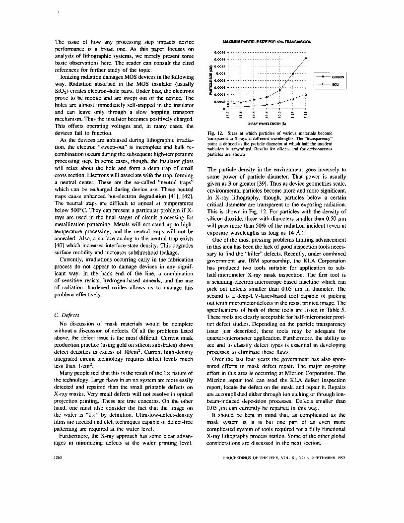
Fig. 12. Sizes at which particles of various materials become transparent to X-rays at different wavelengths. The “transparency” point is defined as the particle diameter at which half the incident radiation is transmitted. Results for silicate and for carbonaceous particles are shown
The particle density in the environment goes inversely to some power of particle diameter. That power is usually given as 3 or greater [39]. Thus as device geometries scale, environmental particles become more and more significant. In X-ray lithography, though, particles below a certain critical diameter are transparent to the exposing radiation. This is shown in Fig. 12. For particles with the density of silicon dioxide, those with diameters smaller than 0.50 pm will pass more than 50% of the radiation incident (even at exposure wavelengths as long as 14 A.)
One of the most pressing problems limiting advancement in this area has been the lack of good inspection tools neces- sary to find the “killer” defects. Recently, under combined government and IBM sponsorship, the KLA Corporation has produced two tools suitable for application to sub- half-micrometer X-ray mask inspection. The first tool is a scanning-electron-microscope-based machine which can pick out defects smaller than 0.05 pm in diameter. The second is a deep-UV-laser-based tool capable of picking out tenth micrometer defects in the resist printed image. The specifications of both of these tools are listed in Table 5. These tools are clearly acceptable for half-micrometer prod- uct defect studies. Depending on the particle transparency issue just described, these tools may be adequate for quarter-micrometer application. Furthermore, the ability to see and to classify defect types is essential in developing processes to eliminate these flaws.
Over the last four years the government has also spon- sored efforts in mask defect repair. The major on-going effort in this area is occurring at Micrion Corporation. The Micrion repair tool can read the KLA defect inspection report, locate the defect on the mask, and repair it. Repairs are accomplished either through ion etching or through ion- beam-induced deposition processes. Defects smaller than 0.05 pm can currently be repaired in this way.
It should be kept in mind that, as complicated as the mask system is, it is but one part of an even more complicated system of tools required for a fully functional X-ray lithography process station. Some of the other global considerations are discussed in the next section.
1260 PROCEEDINGS OF THE IEEE, VOL. 81, NO. 9, SEFTEMBER 1993
Table 5 Approaches to Mask Defect Inspection
A Comparison of UV and Electron-Beam
UVIS
Medium
Highest Sensitivity
Min. Line Width
Inspection time at max. sens.
Min. insp. time at 0.1 microns
Pixel Size
DefecVpixel sire ratio
Max. Processing Rate
Mounting
Footprint
Monitor Wafer (wafer w/resist) Optical mask (Trans. & Refi.) Phase Shift Mask'
0.1 microns
0.25 microns
10 min/sq cm**
2.5 min/sq. cmt
0.12 microns
0.8
50 Megapixeis/sec
Bulkhead
w x 7 2 " 30" x 40" 2 ea.
Inspection Station Height 72"
Linear Wail Space 8'
E-Beam
X-Ray mask Monitor Wafer (conducting)
0.05 microns
0.15 microns
27 min/sq.cm
6.75 min/sq.cm
0.03 microns
1.5
100 Megapixeidsec
Bulkhead
7 0 x loo" 2 5 x 32' 3 ea. w x 4 0 48" x 4 8 (vacuum p.)
104"
15'
^Under investigation "UVIS Specification #With high speed option for UViS
IV. X-RAY SYSTEM DEVELOPMENT-SOURCES, ALIGNERS, AND BEAMLINES
In the preceeding sections of this paper, the two major barriers to the insertion of X-ray technology were outlined. Electron-beam pattern placement and the fabrication of defect-free masks are the current priority issues in the development of this technology. This is not to say that other ancillary technologies are unimportant, In fact, X-ray lithography is, truly, an "array" of technologies-of which each element interacts with others to form a smoothly func- tioning system. Key elements of this system are described below.
A. Sources The first X-ray source employed in Smith's pioneering
effort [43] was a familiar X-ray tube. Variants of these sources are used for medical X-rays as well as for diffrac- tion and fluorescence studies. The tube works by creating an electron beam in a vacuum. This beam hits a metal target. The interaction of the electron beam with the target creates X-rays in two ways.
The incident electrons are energetic enough (> 1 keV) to create an ionization of a core electron in the target. Outer shell electrons "cascade" down to fill the core hole, emitting X-rays on each transition to the final core state. The result is a group of closely spaced X-ray lines corresponding to the series of all possible transitions between two electron shells; a number of these tightly spaced groupings can appear, each corresponding to transitions between different shells. The tightly spaced series of emission lines is designated by the shell representing the final resting place of the electron, and the specific transition is designated by a lower case Greek letter. For example, the A1 K a line corresponds to the most energetic transition to the K-shell for aluminum (1.49 keV).
Electrons striking the metal target are redirected and slowed down through inelastic collisions. Changing the direction and decelerating the charged particle leads to broad band X-ray emission. X-rays will be emitted as a continuum extending from a maximum energy equal to the energy of incidence (the tubes' short-wavelength limit) extending out to zero. The peak of this continuum is usually about one-third the maximum energy, dropping rapidly as the short-wavelength limit is reached, and somewhat more slowly as the zero of energy is approached. This radiation is frequently referred to as Bremstrahlung (braking radiation).
In most X-ray lithographic applications, an optimum X- ray excitation line is chosen. The line must be energetic enough to pass through the mask, but not so energetic as to pass through the opaque absorber or through the resist material. Ideally, about 10-20 % of the incident radiation should be absorbed in the resist. Less energy absorbed would lead to long exposure times; larger absorption would yield a graded energy deposition profile in the resist. The graded profile would create sloped sidewalls and poor control of critical dimensions (CD's). Line energies in a range from about 1-2 keV are usually chosen to meet these criteria. While the continuum clearly has some effect on exposure, the bulk of its spectrum is too energetic or too soft to expose resist.
For the purposes of estimating speed, we neglect the continuum and focus on the line. The X-ray power density incident on the mask Pd is given by the formula
where q is the line conversion efficiency (usually about d is the source-to-mask distance, and P is the power
the electron beam dissipates in the target of the tube. Line conversion efficiency is defined as the ratio of the electron input power to the X-ray output power. P is determined by multiplying the tube's cathode-to-anode bias by the tube current. A tube operating at 50 kV, drawing 50 mA dissipates 2.5 kW. At a source-to-mask working distance of 10 cm, power density is about 2 x mW/cm2 on the mask. The incident dose required to fully expose resist is known as the resist sensitivity. Sensitivity is, thus, wavelength-dependent. In the range of wavelegths of interest to lithography, the fastest resists have sensitivities in excess of 10 mJ/cm2. This would require exposure times close to 10 min for typical tube power densities incident. These exposure rates are far too slow for commercial applications, but research projects in X-ray lithography are frequently accomplished using tube sources.
A number of attempts have been made to increase the tube X-ray intensity [44]. These generally involve tech- niques for increasing the maximum power loading on the target. In the past, water-cooled rotating anode tubes have been used. Mechanical rotation of the anode distributes power over a larger area and water carries heat away. In some systems, the water is actually allowed to boil, forming small bubbles which are carried away by high-pressure water streams. Even with these "nucleate boiling" sources, useful tube power has not exceeded 25 kW.
PECKERAR AND MALDONADO: X-RAY LITHOGRAPHY 1261
/ Opaquefeature
Wafer P-------- a-+& Penumbral Undercut, s
Point source
Opaque feature
boundqpOSition1
wafer position 1
wafer position 2 r boundary position 2
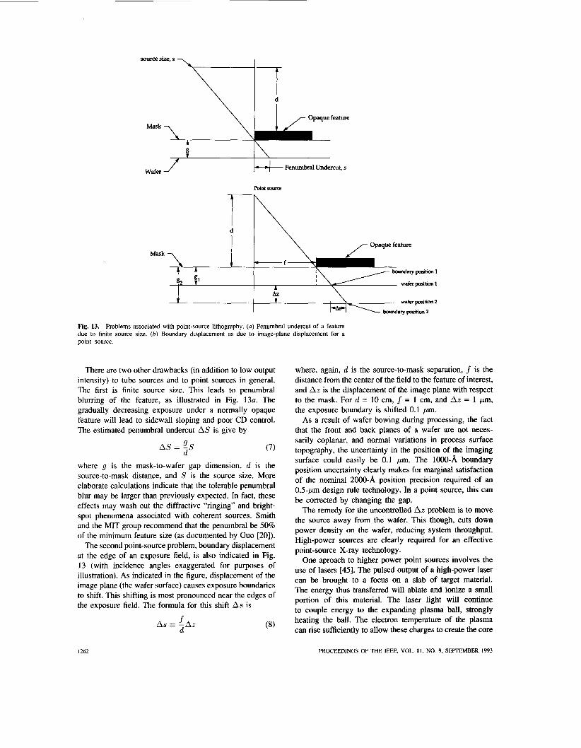
Fig. 13. Problems associated with point-source lithography. (a) Penumbral undercut of a feature due to finite source size. (b ) Boundary displacement as due to image-plane displacement for a point source.
There are two other drawbacks (in addition to low output intensity) to tube sources and to point sources in general. The first is finite source size. This leads to penumbral blurring of the feature, as illustrated in Fig. 13a. The gradually decreasing exposure under a normally opaque feature will lead to sidewall sloping and poor CD control. The estimated penumbral undercut AS is give by
(7) 9 d
A S = -S
where g is the mask-to-wafer gap dimension, d is the source-to-mask distance, and S is the source size. More elaborate calculations indicate that the tolerable penumbral blur may be larger than previously expected. In fact, these effects may wash out the diffractive “ringing” and bright- spot phenomena associated with coherent sources. Smith and the MIT group recommend that the penumbral be 50% of the minimum feature size (as documented by Guo [20]).
The second point-source problem, boundary displacement at the edge of an exposure field, is also indicated in Fig. 13 (with incidence angles exaggerated for purposes of illustration). As indicated in the figure, displacement of the image plane (the wafer surface) causes exposure boundaries to shift. This shifting is most pronounced near the edges of the exposure field. The formula for this shift As is
(8) f AS = -Az d
where, again, d is the source-to-mask separation, f is the distance from the center of the field to the feature of interest, and AZ is the displacement of the image plane with respect to the mask. For d = 10 cm, f = 1 cm, and AZ = 1 pm, the exposure boundary is shifted 0.1 pm.
As a result of wafer bowing during processing, the fact that the front and back planes of a wafer are not neces- sarily coplanar, and normal variations in process surface topography, the uncertainty in the position of the imaging surface could easily be 0.1 pm. The lO00-8, boundary position uncertainty clearly makes for marginal satisfaction of the nominal 2000-8, position precision required of an 0.5-pm design rule technology. In a point source, this can be corrected by changing the gap.
The remedy for the uncontrolled AZ problem is to move the source away from the wafer. This though, cuts down power density on the wafer, reducing system throughput. High-power sources are clearly required for an effective point-source X-ray technology.
One aproach to higher power point sources involves the use of lasers [45]. The pulsed output of a high-power laser can be brought to a focus on a slab of target material. The energy thus transferred will ablate and ionize a small portion of this material. The laser light will continue to couple energy to the expanding plasma ball, strongly heating the ball. The electron temperature of the plasma can rise sufficiently to allow these charges to create the core
I262 PROCEEDINGS OF THE IEEE, VOL. 81, NO. 9, SEPTEMBER 1993
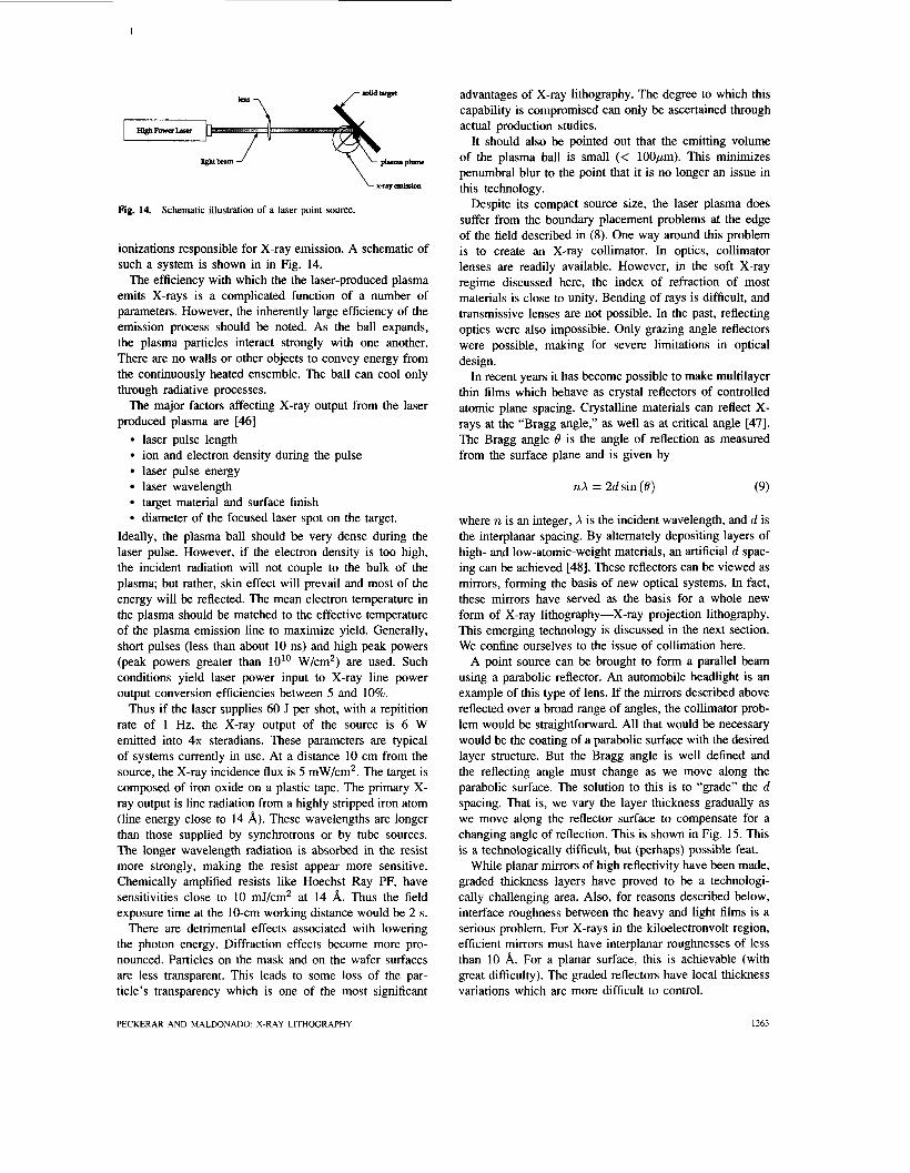
Fig. 14. Schematic illustration of a laser point source.
ionizations responsible for X-ray emission. A schematic of such a system is shown in in Fig. 14.
The efficiency with which the the laser-produced plasma emits X-rays is a complicated function of a number of parameters. However, the inherently large efficiency of the emission process should be noted. As the ball expands, the plasma particles interact strongly with one another. There are no walls or other objects to convey energy from the continuously heated ensemble. The ball can cool only through radiative processes.
The major factors affecting X-ray output from the laser produced plasma are [46]
laser pulse length ion and electron density during the pulse laser pulse energy laser wavelength target material and surface finish diameter of the focused laser spot on the target.
Ideally, the plasma ball should be very dense during the laser pulse. However, if the electron density is too high, the incident radiation will not couple to the bulk of the plasma; but rather, skin effect will prevail and most of the energy will be reflected. The mean electron temperature in the plasma should be matched to the effective temperature of the plasma emission line to maximize yield. Generally, short pulses (less than about 10 ns) and high peak powers (peak powers greater than lo1’ W/cm2) are used. Such conditions yield laser power input to X-ray line power output conversion efficiencies between 5 and 10%.
Thus if the laser supplies 60 J per shot, with a repitition rate of 1 Hz, the X-ray output of the source is 6 W emitted into 4a steradians. These parameters are typical of systems currently in use. At a distance 10 cm from the source, the X-ray incidence flux is 5 mW/cm2. The target is composed of iron oxide on a plastic tape. The primary X- ray output is line radiation from a highly stripped iron atom (line energy close to 14 8). These wavelengths are longer than those supplied by synchrotrons or by tube sources. The longer wavelength radiation is absorbed in the resist more strongly, making the resist appear more sensitive. Chemically amplified resists like Hoechst Ray PF, have sensitivities close to 10 mJ/cm2 at 14 A. Thus the field exposure time at the IO-cm working distance would be 2 s.
There are detrimental effects associated with lowering the photon energy. Diffraction effects become more pro- nounced. Particles on the mask and on the wafer surfaces are less transparent. This leads to some loss of the par- ticle’s transparency which is one of the most significant
advantages of X-ray lithography. The degree to which this capability is compromised can only be ascertained through actual production studies.
It should also be pointed out that the emitting volume of the plasma ball is small (< 100pm). This minimizes penumbral blur to the point that it is no longer an issue in this technology.
Despite its compact source size, the laser plasma does suffer from the boundary placement problems at the edge of the field described in (8). One way around this problem is to create an X-ray collimator. In optics, collimator lenses are readily available. However, in the soft X-ray regime discussed here, the index of refraction of most materials is close to unity. Bending of rays is difficult, and transmissive lenses are not possible. In the past, reflecting optics were also impossible. Only grazing angle reflectors were possible, making for severe limitations in optical design.
In recent years it has become possible to make multilayer thin films which behave as crystal reflectors of controlled atomic plane spacing. Crystalline materials can reflect X- rays at the “Bragg angle,” as well as at critical angle [47]. The Bragg angle 0 is the angle of reflection as measured from the surface plane and is given by
nX = 2d sin ( e ) (9)
where n is an integer, X is the incident wavelength, and d is the interplanar spacing. By alternately depositing layers of high- and low-atomic-weight materials, an artificial d spac- ing can be achieved [48]. These reflectors can be viewed as mirrors, forming the basis of new optical systems. In fact, these mirrors have served as the basis for a whole new form of X-ray lithography-X-ray projection lithography. This emerging technology is discussed in the next section. We confine ourselves to the issue of collimation here.
A point source can be brought to form a parallel beam using a parabolic reflector. An automobile headlight is an example of this type of lens. If the mirrors described above reflected over a broad range of angles, the collimator prob- lem would be straightforward. All that would be necessary would be the coating of a parabolic surface with the desired layer structure. But the Bragg angle is well defined and the reflecting angle must change as we move along the parabolic surface. The solution to this is to “grade” the d spacing. That is, we vary the layer thickness gradually as we move along the reflector surface to compensate for a changing angle of reflection. This is shown in Fig. 15. This is a technologically difficult, but (perhaps) possible feat.
While planar mirrors of high reflectivity have been made, graded thickness layers have proved to be a technologi- cally challenging area. Also, for reasons described below, interface roughness between the heavy and light films is a serious problem. For X-rays in the kiloelectronvolt region, efficient mirrors must have interplanar roughnesses of less than 10 8. For a planar surface, this is achievable (with great difficulty). The graded reflectors have local thickness variations which are more difficult to control.
PECKERAR AND MALDONADO: X-RAY LITHOGRAPHY 1263
GRADED MULTILAYER!+
SOURCE
Fig. 15. to allow for a changing angle of reflection.
Parabolic multilayer collimator with graded “d spacing”
(b)
Fig. 16. The Kumakhov lens collimator concept. (a)A single fiber in a fiber-bundle Kumakhov lens. (b)A completed lens assembly.
Recently, an intriguing alternative to mirror collimators has appeared [49], [50]. In this approach, hollow glass fibers are used as X-ray light guides. The fibers can be bundled together, shaped, and polished on the ends and “wired” to bring the light to a focus through a series of grazing-angle reflections within the tubular hollow. This is shown in Fig. 16. A considerable amount of activity is currently directed toward developing these fiber bundles as point-source collimators.
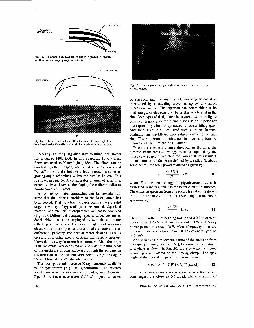
All of the collimator approaches thus far described as- sume that the “debris” problem of the laser source has been solved. That is, when the laser beam strikes a solid target, a variety of types of ejecta are created. Vaporized material and “bullet” microparticles are easily observed (Fig. 17). Differential pumping, special target designs or debris shields must be employed to keep the collimator reflecting surfaces, and the X-ray masks and windows clean. Current laser-plasma sources make effective use of differential pumping and special target designs. Here, a pressure differential across an X-ray transmissive aperture blows debris away from sensitice surfaces. Also, the target is an iron oxide layer deposited on a polymer thin film. Most of the ejecta are thrown backward through the polymer in the direction of the incident laser beam. X-rays propagate forward toward the resist-coated wafer.
The most powerful source of X-rays currently available is the synchrotron [Sl]. The synchrotron is an electron accelerator which works in the following way. Consider Fig. 18. A linear accelerator (LINAC) injects a packet
Fig. 17. Ejecta produced by a high-power laser pulse incident on a solid target.
of electrons into the main accelerator ring where it is intercepted by a traveling wave set up by a klystron microwave source. The injection can occur either at its final energy, or electrons may be further accelerated in the ring. Both types of design have been executed. In the figure provided, a general-purpose ring serves as an injector for a compact ring which is optimized for X-ray lithography. Mitsubishi Electric has executed such a design. In most configurations, the LINAC injects directly into the compact ring. The ring beam is maintained in focus and bent by magnets which form the ring “lattice.”
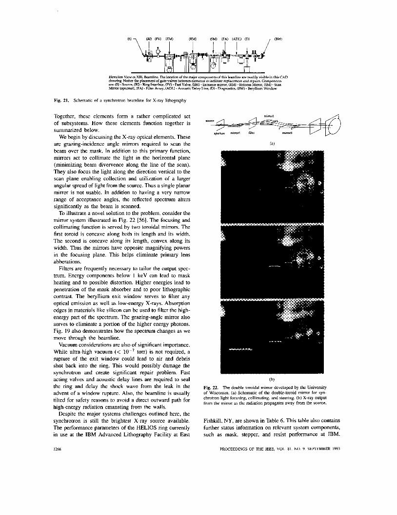
When the electrons change direction in the ring, the electron beam radiates. Energy must be supplied by the microwave source to maintain the current. If we assume a circular motion of the beam defined by a radius R, about some center, the total power radiated is given by
kW 44.8E41 p = -
R3 where E is the beam energy (in gigaelectronvolts), R is expressed in meters, and I is the beam current in amperes. The emission spectrum from this source is peaked, as shown in Fig. 19. The median (or critical) wavelength in the power spectrum E, is
keV . (1 1) E, = - 2 . 2 ~ ~
R Thus a ring with a 2-m bending radius and a 0.2-A current, operating at 1 GeV will put out about 9 kW.s of X-ray power peaked at about 1 keV. Most lithography rings are designed to deliver between 5 and 10 kW of energy peaked at 1 keV.
As a result of the relativistic nature of the emission from the rapidly moving electrons [52], the emission is confined to a plane as shown in Fig. 20. Light emerges in a cone whose apex is centered on the moving charge. The apex angle of the cone 0, is given by the expression
< B c 2 >0.5= (1957.OE)-’(mrad) (12)
where E is, once again, given in gigaelectronvolts. Typical cone angles are close to 0.5 mrad. The divergence of
I264 PROCEEDINGS OF THE IEEE, VOL. S I , NO. 9. SEPTEMBER 1993
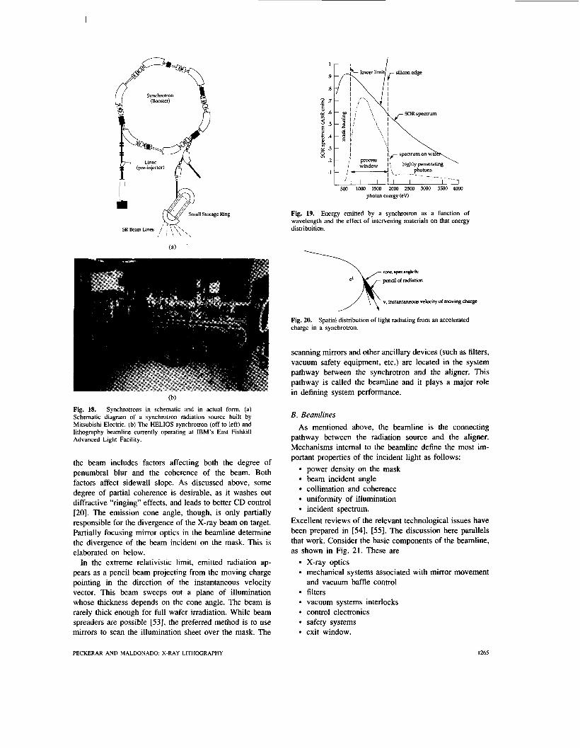
(b)
Fig. 18. Synchrotrons in schematic and in actual form. (a) Schematic diagram of a synchrotron radiation source built by Mitsubishi Electric. (b) The HELIOS synchrotron (off to left) and lithography beamline currently operating at IBM’s East Fishkill Advanced Light Facility.
the beam includes factors affecting both the degree of penumbral blur and the coherence of the beam. Both factors affect sidewall slope. As discussed above, some degree of partial coherence is desirable, as it washes out diffractive “ringing” effects, and leads to better CD control [20]. The emission cone angle, though, is only partially responsible for the divergence of the X-ray beam on target. Partially focusing mirror optics in the beamline determine the divergence of the beam incident on the mask. This is elaborated on below.
In the extreme relativistic limit, emitted radiation ap- pears as a pencil beam projecting from the moving charge pointing in the direction of the instantaneous velocity vector. This beam sweeps out a plane of illumination whose thickness depends on the cone angle. The beam is rarely thick enough for full wafer irradiation. While beam spreaders are possible [53], the preferred method is to use mirrors to scan the illumination sheet over the mask. The
I
I 1
i process I f 1 1 w,,,dow I: hghlypenetrat~ng
’ + c l . - - - -. photons
- - _ f ! I I ! I 1 I 1 1
500 loo0 1500 20m 2500 3ooo 3 m m photon energy (em
Fig. 19. Energy emitted by a synchrotron as a function of wavelength and the effect of intervening materials on that energy distribuition.
cone, apex angle Oc
penal of radiation
v, instantaneous velocity of moving charge
Fig. 20. Spatial distribution of light radiating from an accelerated charge in a synchrotron.
scanning mirrors and other ancillary devices (such as filters, vacuum safety equipment, etc.) are located in the system pathway between the synchrotron and the aligner. This pathway is called the beamline and it plays a major role in defining system performance.
B. Beamlines As mentioned above, the beamline is the connecting
pathway between the radiation source and the aligner. Mechanisms intemal to the beamline define the most im- portant properties of the incident light as follows:
power density on the mask beam incident angle collimation and coherence uniformity of illumination incident spectrum.
Excellent reviews of the relevant technological issues have been prepared in [54], [ S I . The discussion here parallels that work. Consider the basic components of the beamline, as shown in Fig. 21. These are
X-ray optics mechanical systems associated with mirror movement and vacuum baffle control filters vacuum systems interlocks control electronics safety systems exit window.
PECKERAR AND MALDONADO: X-RAY LITHOGRAPHY I265
Elevation View of XRL Beamline. The location of the mapr components of this leamline are readily visible in this CAD drawing. Notice the placement of gate-valves between elements to facilitate replacement and repairs. Components are: (S) -Source, (RD - Ring Interface, (Fv) - Fast Valve, (EM) - Entrance mirror, (RM) - Refocus Mirror, (SM) - Scan Mirror (optional), (FA) -Filter Array, (ADL) - Amustic Delay Line, (D) - Diagnostics, (BW) - Beryllium Window.
Fig. 21. Schematic of a synchrotron beamline for X-ray lithography
Together, these elements form a rather complicated set of subsystems. How these elements function together is summarized below.
We begin by discussing the X-ray optical elements. These are grazing-incidence angle mirrors required to scan the beam over the mask. In addition to this primary function, mirrors act to collimate the light in the horizontal plane (minimizing beam divervence along the line of the scan). They also focus the light along the direction vertical to the scan plane enabling collection and utilization of a larger angular spread of light from the source. Thus a single planar mirror is not usable. In addition to having a very narrow range of acceptance angles, the reflected spectrum alters significantly as the beam is scanned.
To illustrate a novel solution to the problem, consider the mirror system illustrated in Fig. 22 [56]. The focusing and collimating function is served by two toroidal mirrors. The first toroid is concave along both its length and its width. The second is concave along its length, convex along its width. Thus the mirrors have opposite magnifying powers in the focusing plane. This helps eliminate primary lens abberations.
Filters are frequently necessary to tailor the output spec- trum. Energy components below 1 keV can lead to mask heating and to possible distortion. Higher energies lead to penetration of the mask absorber and to poor lithographic contrast. The beryllium exit window serves to filter any optical emission as well as low-energy X-rays. Absorption edges in materials like silicon can be used to filter the high- energy part of the spectrum. The grazing-angle mirror also serves to eliminate a portion of the higher energy photons. Fig. 19 also demonstrates how the spectrum changes as we move through the beamline.
Vacuum considerations are also of significant importance. While ultra-high vacuum (< lop7 torr) is not required, a rupture of the exit window could lead to air and debris shot back into the ring. This would possibly damage the synchrotron and create significant repair problem. Fast acting valves and acoustic delay lines are required to seal the ring and delay the shock wave from the leak in the advent of a window rupture. Also, the beamline is usually tilted for safety reasons to avoid a direct outward path for high-energy radiation emanating from the walls.
Despite the major systems challenges outlined here, the synchrotron is still the brightest X-ray source available. The performance parameters of the HELIOS ring currently in use at the IBM Advanced Lithography Facility at East
Y) Y)
(b)
Fig. 22. The double toroidal mirror developed by the University of Wisconsin. (a) Schematic of the double-toroid mirror for syn- chrotron light focusing, collimating, and steering. (b) X-ray output from the mirror as the radiation propagates away from the source.
Fishkill, NY, are shown in Table 6. This table also contains further status information on relevant system components, such as mask, stepper, and resist performance at IBM.
I266 PROCEEDINGS OF THE IEEE, VOL. 81, NO. 9, SEPTEMBER 1993
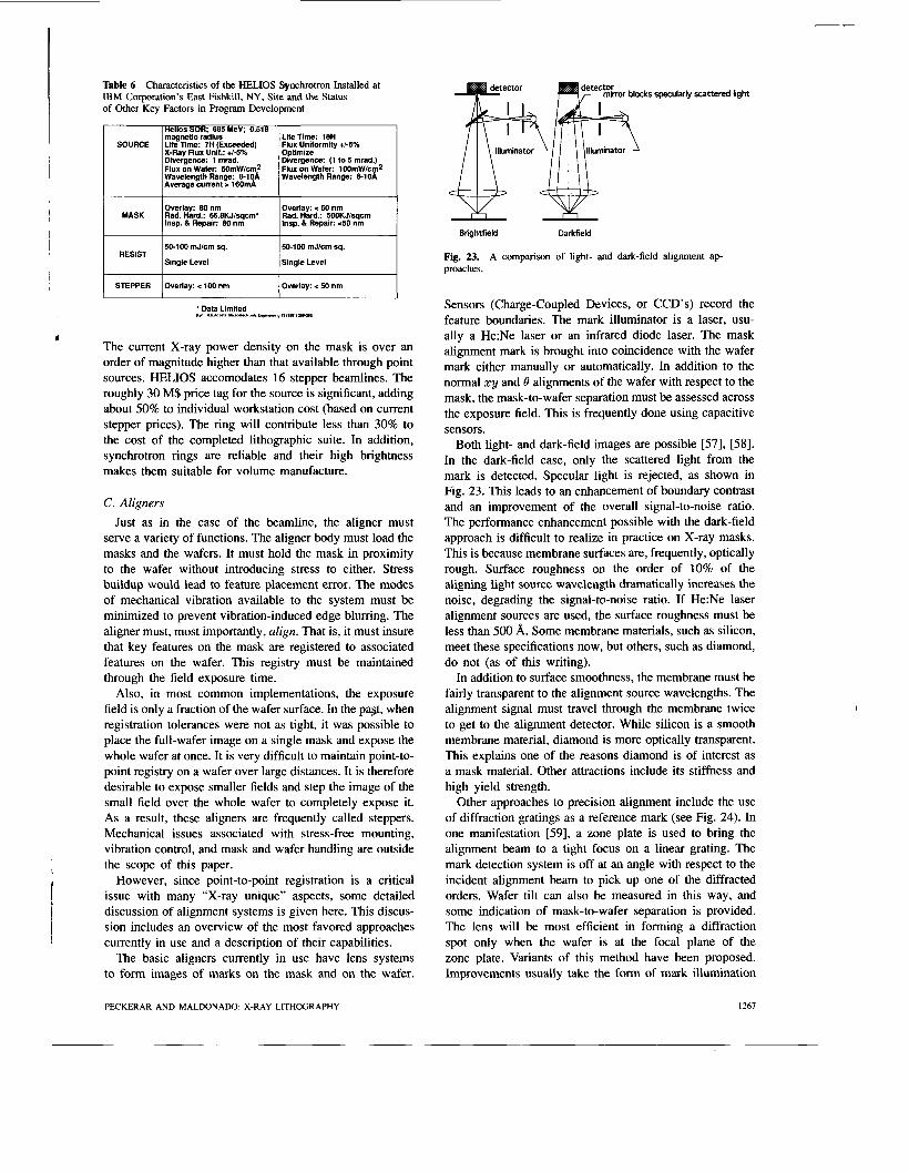
I
RESIST
STEPPER
Table 6 Characteristics of the HELIOS Synchrotron Installed at IBM Corporation’s East Fishkill, NY, Site and the Status of Other Key Factors in Program Development
50-100 mJ/cm sq.
Single Level Single Level
Overlay: < 100 nm Overlay: 50 nm
50-100 mJ/cm sq.
magnetic radius Life lime: 18H SOURCE Life Time: 7H (Exceeded) Flux Uniformity +/-5%
X-Ray Flux Unif.: +/-5% Optimize Divergence: 1 mad. Flux on Wafer: 50mW/cm2 Wavelength Range: a i o A Average current > 16OmA
Divergence: (1 to 5 mrad.) Flux on Wafer: 1WmW/cm2 Wavelength Range: a i o A
Overlay: 80 nm
Insp. & Repair: 80 nm
Overlay: c 50 nm
Insp. & Repair: e50 nm MASK Rad. Hard.: 66.8KJkqcm’ Rad. Hard.: 5OOKJ/sqcm
The current X-ray power density on the mask is over an order of magnitude higher than that available through point sources. HELIOS accomodates 16 stepper beamlines. The roughly 30 M$ price tag for the source is significant, adding about 50% to individual workstation cost (based on current stepper prices). The ring will contribute less than 30% to the cost of the completed lithographic suite. In addition, synchrotron rings are reliable and their high brightness makes them suitable for volume manufacture.
C . Aligners Just as in the case of the beamline, the aligner must
serve a variety of functions. The aligner body must load the masks and the wafers. It must hold the mask in proximity to the wafer without introducing stress to either. Stress buildup would lead to feature placement error. The modes of mechanical vibration available to the system must be minimized to prevent vibration-induced edge blurring. The aligner must, most importantly, align. That is, it must insure that key features on the mask are registered to associated features on the wafer. This registry must be maintained through the field exposure time.
Also, in most common implementations, the exposure field is only a fraction of the wafer surface. In the pag, when registration tolerances were not as tight, it was possible to place the full-wafer image on a single mask and expose the whole wafer at once. It is very difficult to maintain point-to- point registry on a wafer over large distances. It is therefore desirable to expose smaller fields and step the image of the small field over the whole wafer to completely expose it. As a result, these aligners are frequently called steppers. Mechanical issues associated with stress-free mounting, vibration control, and mask and wafer handling are outside the scope of this paper.
However, since point-to-point registration is a critical issue with many “X-ray unique” aspects, some detailed discussion of alignment systems is given here. This discus- sion includes an overview of the most favored approaches currently in use and a description of their capabilities.
The basic aligners currently in use have lens systems to form images of marks on the mask and on the wafer.
PECKERAR AND MALDONADO: X-RAY LITHOGRAPHY
detector dett
Illuminator 1 & U speculariy xattered
minator 1
Brightfield Darkfield
Fig. 23. proaches.
A comparison of light- and dark-field alignment ap-
light
Sensors (Charge-Coupled Devices, or CCD’s) record the feature boundaries. The mark illuminator is a laser, usu- ally a He:Ne laser or an infrared diode laser. The mask alignment mark is brought into coincidence with the wafer mark either manually or automatically. In addition to the normal xy and 8 alignments of the wafer with respect to the mask, the mask-to-wafer separation must be assessed across the exposure field. This is frequently done using capacitive sensors.
Both light- and dark-field images are possible [571, [58]. In the dark-field case, only the scattered light from the mark is detected. Specular light is rejected, as shown in Fig. 23. This leads to an enhancement of boundary contrast and an improvement of the overall signal-to-noise ratio. The performance enhancement possible with the dark-field approach is difficult to realize in practice on X-ray masks. This is because membrane surfaces are, frequently, optically rough. Surface roughness on the order of 10% of the aligning light source wavelength dramatically increases the noise, degrading the signal-to-noise ratio. If He:Ne laser alignment sources are used, the surface roughness must be less than 500 A. Some membrane materials, such as silicon, meet these specifications now, but others, such as diamond, do not (as of this writing).
In addition to surface smoothness, the membrane must be fairly transparent to the alignment source wavelengths. The alignment signal must travel through the membrane twice to get to the alignment detector. While silicon is a smooth membrane material, diamond is more optically transparent. This explains one of the reasons diamond is of interest as a mask material. Other attractions include its stiffness and high yield strength.
Other approaches to precision alignment include the use of diffraction gratings as a reference mark (see Fig. 24). In one manifestation [59], a zone plate is used to bring the alignment beam to a tight focus on a linear grating. The mark detection system is off at an angle with respect to the incident alignment beam to pick up one of the diffracted orders. Wafer tilt can also be measured in this way, and some indication of mask-to-wafer separation is provided. The lens will be most efficient in forming a diffraction spot only when the wafer is at the focal plane of the zone plate. Variants of this method have been proposed. Improvements usually take the form of mark illumination
I261
wafer
mask zone plate
I \- I
wafer - n
1.5 pm
(perpendicular to alignment direction) (parallel to alignment direction)
Fig. 24. An alignment system using zone plates and diffraction gratings.
by multiple beams. These beams can differ in wavelength, polarization sense, or in the phase of the time modulation of incident pulse intensity. Balance of output intensity of diffracted orders from these multiple beams is sought. The Wisconsin group has demonstrated 300-8,, 3a point repositioning capability with this technique [60].
The problem of alignment is common to both X-ray and optical projection systems. It should be pointed out that this problem is, essentially, 1 x in nature for both approaches. The point on the mask must be aligned accurately with respect to the l x image on the printed surface. Prob- lems in point repositioning in electron-beam mask-making tools are largely the same as those encountered in stepper alignment. The accuracy of the interferometrically driven stage positioning, the issues of mechanical stability, and environmental effects are all largely common as we move from approach to approach. Thus the fact that this task can be accomplished for a single stepper field is a “proof-of- principle” that this can be accomplised by the electron-beam tool on the mask at l x .
This concludes our review of the key issues associated with the inclusion of X-ray proximity printing into the microelectronics manufacturing toolbox. In the next section, we tum our attention to altemative systems which synthe- size optical stepper technology with soft X-ray sources and which may become important in the next century if present limitations are overcome.
V. FUTURE SYSTEMS Proponents of proximity printing feel that the lenseless
simplicity of their approach more than offsets the difficul- ties relating to smaller feature sizes and tighter tolerances on the mask. They will also cite the “proof-of-principle’’ argument for feature placement given above. But mask
1268
making process is easier in the n x case. It is easier to spot defects and placement fidelity improves within an exposure field on demagnification. In order to retain the high resolution and good process latitude of X-ray lithography and to capture the advantage of nx reduction steppers, projection X-ray lithography has been proposed.
Projection systems make use of the multilayer approach described above to create X-ray reflecting mirrors. These mirrors form the reflecting lenses required for a projection stepper. One example of such a system is shown Fig. 25. Note that for this particular system, there are seven reflect- ing surfaces (including the mask). The system throughput (number of square centimeters of resist exposed per second) is given by the expression
T = P,W3R7/S (13)
where P, is the source power on target (mW/cm2), W is the window transmissivity (three vacuum windows are required for this system), T is the mask reflectivity, and S is the sensitivity of the resist (mJ/cm2). While the system is complicated, it is no more complicated than existing optical stepper lens designs. In addition, feature size reduction factors of 20 are possible with this system operating as a 0.15-pm printer.
Note that the throughput goes as the seventh power (seven reflecting surfaces) of reflectivity. This, of course, assumes that the mirror reflectivities are all equal. For reflectivities as high as 70%, the intensity at the wafer plane is reduced to about 8% of that available from the source. Thus high mirror reflectivities over the exposure field are required. In addition, in order to create an aberration-free system, aspheric lenses with surface figure control of better than 20 8, are required. These are daunting feats by the standards of curent technology. The hope is to have some preliminary success with small-field systems by the middle
PROCEEDINGS OF THE IEEE, VOL. 81, NO. 9, SEREMBER 1993
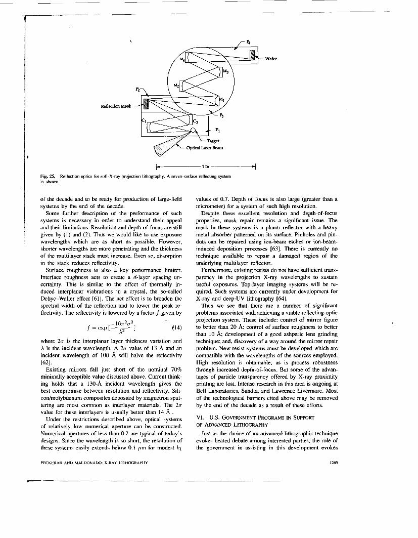
Refledion Mask
I
l--1m-
Fig. 25. is shown.
Reflection optics for soft-X-ray projection lithography. A seven-surface reflecting system
of the decade and to be ready for production of large-field systems by the end of the decade.
Some further description of the performance of such systems is necessary in order to understand their appeal and their limitations. Resolution and depth-of-focus are still given by (1) and (2). Thus we would like to use exposure wavelengths which are as short as possible. However, shorter wavelengths are more penetrating and the thickness of the multilayer stack must increase. Even so, absorption in the stack reduces reflectivity.
Surface roughness is also a key performance limiter. Interface roughness acts to create a d-layer spacing un- certainty. This is similar to the effect of thermally in- duced interplanar viabrations in a crystal, the so-called Debye-Waller effect [61]. The net effect is to broaden the spectral width of the reflection and to lower the peak re- flectivity. The reflectivity is lowered by a factor f given by
414)
where 2a is the interplanar layer thickness variation and X is the incident wavelength. A 2a value of 13 A and an incident wavelength of 100 8, will halve the reflectivity 1621.
Existing mirrors fall just short of the nominal 70% minimally acceptible value discussed above. Current think- ing holds that a 130-A incident wavelength gives the best compromise between resolution and reflectivity. Sili- con/molybdenum composites deposited by magnetron sput- tering are most common as interlayer materials. The 2u value for these interlayers is usually better than 14 A .
Under the restrictions described above, optical systems of relatively low numerical aperture can be constructed. Numerical apertures of less than 0.2 are typical of today's designs. Since the wavelength is so short, the resolution of these systems easily extends below 0.1 pm for modest Icl
PECKERAR AND MALDONADO: X-RAY LITHOGRAPHY
values of 0.7. Depth of focus is also large (greater than a micrometer) for a system of such high resolution.
Despite these excellent resolution and depth-of-focus properties, mask repair remains a significant issue. The mask in these systems is a planar reflector with a heavy metal absorber patterned on its surface. Pinholes and pin- dots can be repaired using ion-beam etches or ion-beam- induced deposition processes [63]. There is currently no technique available to repair a damaged region of the underlying multilayer reflector.
Furthermore, existing resists do not have sufficient trans- parency in the projection X-ray wavelengths to sustain useful exposures. Top-layer imaging systems will be re- quired. Such systems are currently under development for X-ray and deep-UV lithography [a].
Thus we see that there are a number of significant problems associated with achieving a viable reflecting-optic projection system. These include: control of mirror figure to better than 20 A; control of surface roughness to better than 10 A; development of a good ashperic lens grinding technique; and, discovery of a way around the mirror repair problem. New resist systems must be developed which are compatible with the wavelengths of the sources employed. High resolution is obtainable, as is process robustness through increased depth-of-focus. But some of the advan- tages of particle transparency offered by X-ray proximity printing are lost. Intense research in this area is ongoing at Bell Laboratories, Sandia, and Lawrence Livermore. Most of the technological barriers cited above may be removed by the end of the decade as a result of these efforts.
VI. U.S. GOVERNMENT PROGRAMS IN SUPPORT OF ADVANCED LITHOGRAPHY
Just as the choice of an advanced lithographic technique evokes heated debate among interested parties, the role of the govemment in assisting in this development evokes
1269
an equally impassioned response.$ubtle (or not so subtle) changes in administrative position and agency responsibil- ity make long-range, consistent planning difficult. Despite these difficulties, the positive role of the government in the history of microlithography and in the history of semicon- ductor technology as a whole is undeniable.
Markel, King, and Offner were sponsored by the gov- ernment in their development of the Micralign tool at Perkin Elmer Corporation. The Micralign system, the first projection lithography engine was, perhaps, the key tool ushering in the LSI and VLSI eras. GCA Corporation received government support for the development of its deep-UV stepper. Kilby was working on a govemment- sponsored project when he developed the first integrated circuit. In all cases, government support was timely and crucial in insuring the success of these undertakings.
In all the cases cited above, the source of funds was a military agency. The Department of Defense has, in the past, been an important user of semiconductor technologies. The significance of high-speed digital processors and sensor systems has been underscored in recent history. While the synergy demonstrated between military and commer- cial interests may be considered serendipitous, it exists nonetheless.
But defense interests have been specific, reflecting real customer needs. As such, the resulting programs have been structured with well-defined goals. The need for the product has been constant, and government program managers have been willing to include research and development costs into project framework. Thus government sponsorship has pro- vided a fairly constant resource for product improvement, even during hard times.
In recognition of the central importance of lithography in semiconductor technology, the military has sponsored the Advanced Lithography Program since 1988. The global goal of this program is to assist in the achievement of a lithographic technology capable of manufacturing inte- grated circuits utilizing 0.25-pm design groundrules shortly after mid-decade. Subsidiary goals include improvement of yields at more relaxed design rules and the provision of a technology base capable of extension into the &quantum effect regime of device performance.
In order to achieve these goals, program support must be consistent with the evolutionary trends of the industry. Cur- rent industrial development efforts are aimed at near-term improvement of UV and deep-UV optical approaches. Gov- ernment managers defining these goals should be cognizant of this fact. Industry and government/industry consortia (like SEMATECH) have active programs in near-term step- per and optical system improvement. Direct government sponsorship would be redundant in this area. However, much work must be done in ancillary technologies, such as inspection and repair of mask plates, metrology, and pattern generation tool development. Long-range govem- ment support in these areas is symbiotic and beneficial to all lithographies currently in practice.
The long-term nature of the government interest provides further opportunity for long-range development. Specifi-
cally, the Advanced Lithography Program can and does sponsor research into alternatives to near-term industrial pathways. For the reasons outlined above, such explo- ration is prudent. As a given technology matures, the basic physical limitations of the technology are encountered. Certainly, many of these limitations can be overcome through clever design. But the cost and time required to surmount these problems becomes greater as design rules become more challenging. The benefit of introducing a new approach which does not suffer from these same limitations is obvious.
But the selection of such alternate approaches requires great care. It is probably true that a number of nonopti- cal approaches could achieve the quarter-micrometer goal, given enough time and money. As each of these technolo- gies requires major engineering innovation, it is extremely difficult to project time and cost for success for any one method.
Furthermore, given the enormous expense (certainly over 100M$) required to bring about a single generational im- provement in lithographic capability, it would not be pos- sible to fund multiple approaches. Even if the primary lithographic tool were successfully provided, the support and infrastructure technologies would be equally expensive. Each lithographic alternative has unique mask, resist, and pattern generation requirements.
In choosing X-ray technology as the program alternative to current optical approaches, the following issues were considered:
The degree to which the alternative satisfied critical requirements of the quarter-micrometer goal. The extendibility of the alternative to future require- ments. The overlap of infrastructure support technologies and the support technologies of the mainstream optical approaches. The ease with which the alternate technology can be inserted into existing manufacturing lines (as ascer- tained by on-going program efforts and investments in target industries).
The first two of these items refer to the question of ultimate performance. These issues were addressed in great depth above. The second two represent purely programmatic concerns. Almost any advanced technology currently under consideration can be viewed as satisfying the first two items (in some light). Thus the deciding factors rest in consideration of the last two items.
Clearly, a fair fraction of the support technology for optical lithography carries over into the X-ray arena. In fact, for the reasons cited, pattern generation problems may be more easily addressed using X-ray membranes to eliminate substrate backscatter. The inspection and repair tooling is common for X-ray and for optical plates. Alignment systems are also the same. There are key differences between the two technologies (such as the thickness of the opaque portions of the mask and the nx reduction factor of projection systems). But these differences are those which
I
1270 PROCEEDINGS OF THE IEEE, VOL. 81, NO. 9, SEPTEMBER 1993
PROGRAM PHASES PHASE I: BASE TOOL AND PROCESS DEVELOPMENT, CREATNX OF AN EQLIPMENTS INFRASTRUCTURE (EXAMPLES: MICRION, KLA, ETEC. ETC...)
PHASE II: DEVELOPMENT OF A SYSTEMS INFRASTRUCTURE (U. OF WISCONSIN U(POWRE STATIONS, MASK WOP, COOPERATIVE INDUSTRIES ETC.)
PHASE 111: DEVICE c€Kx(sTnATloNs
Fig. 26. Phase development of the Defense Advanced Lithogra- phy Program’s X-ray effort.
the government program can and does address. Thus the X- ray program is truly symbiotic with optics in infrastructure development planning.
The last item of consideration is one in which X-ray technology receives particularly high marks. IBM has made a massive commitment to its development. The exposure source alone (the synchrotron facility at East Fishkill) represents over 20M$ in investment capital. Motorola Cor- poration and AT&T have formed strategic alliances with IBM to develop X-ray lithography processes. In addition, Motorola has established a cooperative development agree- ment with the University of Wisconsin for evaluation of synchrotron systems. AT&T Bell Laboratories has an active program in point-source X-ray lithography. The goal of this program is to determine manufacturing yields with point source systems. The company also has launched a considerable effort in soft-X-ray projection lithography. Some results from this program were previously cited. LockheedISanders Corporation has been applying X-ray technology to the fabrication of Microwave Monolithic Integrated Circuits.
Thus at least four major industrial agencies are currently actively pursuing the technology. Work accomplished by govemment-sponsored programs in this area will clearly not enter a vacuum. In addition, these interested companies provide a customer base for the output of the support tool infrastructure.
At this point, let us consider the basic organization of the govemment program. This is outlined in Fig. 26. A timeline for major milestones is shown in Fig. 27. There are three major developmental phases. The first phase involves the creation of an infrastructure for tool supply. One of the major considerations in this phase is the broad range of application for the targeted tools. In fact one of the tools, a deep-UV inspection system built by KLA Corporation, will be used in a SEMATECH program for phase-shift mask inspection. Other studies, such as those on the application of advanced pattem generation techniques performed at ETEC Corporation, have had impact on routine chrome- plate mask making. The primary focus in this phase was the development of tooling for defect-free X-ray masks. This phase of the project is currently concluding and a defect- free mask process is scheduled to come on line at IBM in the fourth quarter of calendar 1993.
The second phase of effort has already begun. Here, major resource centers are targeted for construction. The first, the synchrotron exposure station at the University of Wisconsin, has reached a sufficient state of completion for the commencement of the joint Motorola/ Wisconsin effort.
UNIVERSITY of WISCONSIN EXPOSURE FACILITY
I
MASK SHOP I
QUARTER MICRON STEPPER I
DEFECT FREE MASKS I
INSPECTION AND REPAIR
I E-BEAM TOOL
I
-1 99Z-----1993-----1994---199S----1996---
Fig. 27. Timeline for key tool and facility deployment for the quarter-micrometer effort.
A major mask development effort is scheduled for launch in the fourth calendar quarter of 1993. The site for this effort has not been decided as of this writing. But its purpose is the spurring of advanced mask pattem generation processes. Some work in advanced optical pattern generation is also contemplated.
The third phase will be that of technology insertion. Here, circuit development programs will be initiated, aimed at improving affordability and performance in military systems.
To conclude, the govemment has put in place a major advanced lithography development effort. That program is structured to support a range of near- and long-term needs of the semiconductor industry without blocking or impeding any one approach. X-ray lithography has been chosen as the primary alternative to optics. This selection was made for its promise of extendibility and its demonstrated near- term performance. But also, and perhaps more importantly, the infrastructure necessary to support this technology is compatible with the evolutionary trend of the industry. A number of major industries have already stepped for- ward to commit the large resource necessary to insure the development and survival of the requisite infrastructure.
The needs of the lithography community are many and vaned. As a result, the problem of technology development here is far more complicated than it is in other areas. The single “flaming insight” has little or no impact when one considers the array of related technologies needed to create generational improvements. Even if the perfectly resolving aligner demonstrating perfect placement were available today, the tool would be useless if the support systems needed to maintain it were flawed or unavailable. The govemment has served as coordinator and mediator, assuring a balanced effort in all areas without blocking future pathways.
VII. CONCLUSIONS In this paper, the fundamental principles of X-ray lithog-
raphy were presented. Resolution limits were shown to be on the order of 0.1 pm for proximity printing using the IO-20-pm mask-to-wafer separations currently main- tainable in manufacturing systems. In addition, sub-tenth- micrometer resolution is possible using soft X-ray projec- tion systems or by going to “microgap” (< 5 pm) or other
PECKERAR AND MALDONADO: X-RAY LITHOGRAPHY 1271
approaches. Process robustness is excellent. Depth of focus is large in proximity and in X-ray projection printing. Prox- imity printing has the advantage of particle transparency due to the relatively short exposure wavelengths employed. High-brightness sources, currently available in the form of synchrotrons and plasma sources (possibly employing some form of radiation collimator) are emerging as viable candidates for stand-alone systems. Thus the problem of source brightness is no longer an issue.
The major drawback to the insertion of X-ray lithography on production line is the lack of availability of suitable X-ray masks. Problems with mask technology are two- fold in nature. First, electron-beam pattem placement is insufficient to meet the requirements of 0.25-pm design rules (assuming a 20% of the feature size requirement). Improvement in electron-beam technology is a requisite for all advanced lithographic approaches. The sliding table concept described above represents a major step forward in this area.
The second problem is that of defects in the mask. One of the major inhibitors to development in this area has been the lack of good inspection tools. Over the last year, this is- sue has been resolved. A high-resolution scanning-electron microscope based inspection tool, the KLA SEMSPEC, has come on line. It is capable of pinpointing 50-nm defects. In addition, the KLA UVIS tool, a deep-UV machine which inspects the printed image, has been demonstrated. The availability of these tools is the major source of optimism regarding the liklihood of a near-term solution to this major roadblock to the insertion of X-ray technology.
But the ultimate decision on the adaptation of any new technology is made in the marketplace. As any tool ap- proaches the end of its useful life, operating costs go up dramatically. These costs relate to tool upkeep and to the purchase of “retrofits” required to meet more aggressive goals. The initial costs required to field a new technology are also large. Once these costs are met, daily operating costs and improvement costs are low.
Note Added in Proof Since the draft of this manuscript went off to press,
another X-ray milestone was achieved. A fully functional 512-kb S U M with a 0.35-pm transistor channel length was fabricated by IBM. The device contained 3.6 million transistors and ranks as one of the densest chips currently in prototype development [65]. Clearly, a defect-free mask had to be made to create this result.
ACKNOWLEDGMENT The authors gratefully acknowledge the contributions
of the following people: Dr. D. Patterson (ARPA), Dr. G. Borsuk (NRL), Dr. E. Dobisz (NRL), Dr. C. Marrian (NRL), Dr. H. Smith (MIT), Dr. R. Engelstadt (University of Wisconsin), Dr. J. Taylor (University of Wisconsin), Dr. F. Cerrina (University of Wisconsin), J. Kelly (IBM), and Ms. H. Ishii (Come11 University).
REFERENCES
R. M. Hill, “The future costs of semiconductor lithography,” J. Vac. Sci. Techol. B , vol. 7, 110.6, p. 1387, 1989. M. Lundstrom and S. Datta, “Physical device simulation in a shrinking world,” IEEE Circuits and Device Mag., vol. 6, no.1, p. 32. 1990. S. P.Murarka and M. C. Peckerar, Electronic Materials: Science And Technology. J. T. Clemens and R. W. Hill, Eds., X-ray Lithography in Japan (JTEC Panel Symp. Proc. available through Loyola College, Baltimore, MD, 1991). E. Barouch, U. Hollerbach, S. A. Orszag, B. Bradie, and M. Peckerar, “Modeling process latitude in uv projection lithogra- phy,“ IEEE Electron Device Let., vol. 12, no. 10, pp. 513-514, 1991, R. Viswanathan, D. Seeger, A. Bright, T. Bucelot, J. Warlau- mont, P. Agnello, and M. Policari, “DRAM fabrication with X-ray lithography,” extended abstract 694 in 4rh In?. Symp. on ULSI Science and Technology (Honolulu, HI, May 16-21),
H. Fukuda, A. Imai, T. Terasawa, and S. Okazaki, “New approach to resolution limit and advanced image formation techniques, in optical lithography,” IEEE Trans. Electron De- vices,vol. 38, no.1, p. 67, 1991. M. D. Levenson, “A novel technique for contrast enhancement in optical lithography,” IEEE Trans. Electron Devices, vol. ED- 29, no. 12, pp. 1828-1836, 1982. R. Acosta, “Stress in silicon membranes,” presented at the Workshop on X-ray Lithography (Brookhaven National Lab- oratory, Nov.17-18, 1986), Rep. BNL-52 046. D. I. Ma, S. B. Qadri, and M. C. Peckerar, “Characterization of thin boron doped membranes by double crystal X-ray to- pography,” J. Vac. Sci. Techol. B , vol. 7, no. 6, pp. 1594-1599, 1989. D. K. Stewart, J. Fuchs, R. A. Grant, and I. Plotnik, “Defect repair for gold absorber/silicon membrane X-ray masks,” Proc. SPIE, vol. 1465, p. 64, 1991. Y. C. Pati, A. Teolis, D. Park, R. Bass, K. Rhee, B. Bradie, and M. C. Peckerar, “An error measure for dose correction in e-beam lithography,” J. Vac. Sci. Technol. B , vol. 8, no. 6, pp.
J. W. Goodman, Introduction to Fourier Optics. San Fran- cisco, CA: McGraw-Hill, 1968. H. Huff, “SEMATECH Silicon Progress Report,” Tech. Rep.
L. K. White, “A model for study of superficial topology for improved lithography,” J. Electrochem. Soc., vol. 132, no. 12, p. 3037, 1985. L. K. White and N. Miszkowski, “Topography-induced thick- ness variation anomalies for spin coated thin films,” J. Vac. Sci. Technol. B, vol. 3, no. 3, p. 862, 1985. S. D. Hector, M. L. Shatterbury, E. H. Anderson, W. Chu, V. V. Wong, and H. I. Smith, “Modeling and experimental verification of illumination and diffraction effects on image quality in X- ray lithography,” .I. Vac. Sci. Technol. B , vol. 10, no. 6, p. 3164, 1992. H. K. Oertel, M. Weisz, H. L. Huber, Y. Vladimirski, and J . Maldonado, “Modeling illumination effects in resist profiles in X-ray lithography,” SPIE, vol. 1465, p. 244, 1991. B. J. Lin, “A comparison of projection and proximity printing from uv to X-ray,” SPIE, vol. 1263, Electron Beam, X-ray And Ion Beam Lithography: Submicrometer Lirhographies, I X , p. 80, 1990. J. Z. Y. Guo, G. Chen, V. White, P. Anderson, and F. Cerrina, “Aerial image formation in synchrotron radiation based lithog- raphy: The whole picture,” J. Vac. Sci. Techol., vol. 63, p. 199, 1990. L. Ocola and F. Cerrina, “Modeling photoelectron effects in X- ray photolithography,” in Proc. MRS 1993 Meet., G. Celler and J. Maldonado, Eds., to be published. M. Born and E. Wolf, Principles Of Optics, 6th ed. Oxford, UK: Pergamon, 1980. G. 0. Reynolds, J. B. De Velis, J. B. Parrent, and B. J. Thomp- son, The New Physical Optics Notebook: Tutorials in Fourier Optics, 2th ed. Bellingham, WA: SPIE Optical Engineering Press, 1989. J. E. Bjorkholm, J. Bokor, L Eichner, R. F. Freeman, J. Gregus, T. E. Jewell, W. M. Mansfield, A. A. MacDowell, E. L. Raab,
Cambridge, MA: Academic Press, 1989.
1993, EC vol. 93-1, p. 989.
1882-1888, 1990.
90070297AA-TR, Aug. 24, 1990.
1272 PROCEEDINGS OF THE IEEE, VOL. 81, NO. 9, SEPTEMBER 1993
W. T. Silvast, L. H. Szeto, D. M. Tennant, W. K. Waskiewicz, D. L. White, 0. R. Wood 11, and J. H. Bruning, “Reduction imaging at 14 nm using multilayer-coated optics: printing of features smaller than 0.1 j”” J. Vac. Sci. Technol. B, vol. 8, no. 6, pp. 1509-1513, 1990. R. Feder, E. Spiller, and J. Topalian, “Electron ranges in photoresist,” J. Vac. Sci. Technol., vol. 12, p. 1332, 1975. K. Early, M. L. Schattenburg, and H. I. Smith, “Absence of resolution degradation in x-ray lithography for X = 4.5 nm to 0.83 nm,” Microelectron. Eng., vol. 11, pp. 317-321, 1990. K. Early, M. L. Schattenberg, D. B. Ulster, M. I. Shepard, and H. I Smith, “Diffraction in proximity x-ray lithography: Com- paring theory and experiment for gratings, lines and spaces,” Microelectron. Eng., vol. 17, pp. 149-152, 1992. J. R. Maldonado, G. A. Coquin, D. Maydan, and S. Somekh, “Spurious effects caused by the continuum radiation and ejected electrons in x-ray lithography,”J. Vac. Sci. Technol., vol. 12, p. 1329, 1975. K. Murata, D. F. Keyser, and C. H. Ting, “Monte Carlo simulation of fast secondary electron production in electron beam resists,”J. Appl. Phys., vol. 52, p. 5985, 1982. K. Murata, “Theoretical studies of the electron scattering effect on developed pattern profiles in X-ray lithography,” J. Appl. Phys., vol. 57, p. 575, 1985. W. H. Steele, Interferometry, 2nd ed. Cambridge, UK: Cam- bridge Univ. Press, 1983. J. W. Robinson, Handbook Of Spectroscopy, vol. I. Cleveland, OH: CRC Press, 1974. C. W. Jurgensen, R. R. Kola, A. E. Novembre, W. W. Tai, J. Frackoviak, L. E. Trimble, and G. K. Celler, “Tungsten patteming for 1 : 1 X-ray masks,” J. Vac. Sci. Technol. B, vol. 9, no. 6, pp. 3280-3286, 1991. Y.-C. Ku, L.-P. Ng, R. Carpenter, K. Lu, H. I. Smith, L. E. Haas, and I. Plotnik, “In situ stress monitoring and deposition of zero-stress W for X-ray masks,” J. Vac. Sci. Technol. B, vol. 9, no. 6, pp. 3297-3305, 1991. I. Shareef, J. R. Maldonado, and D. Katcoff, “Thermal and mechanical model of x-ray lithography masks under short pulse irradiation,” J. Vac. Sci. Technol. B, vol. 7, no. 6, p. 1575, 1989. E. A. Haytcher, R. L. Engelstad, and N. M. Schnurr, “Finite element analysis of dynamic thermal distortions of an X-ray mask for synchrotron radiation lithography,” SPIE, vol. 1671,
W. A. Johnson, R. A. Levy, D. J. Resnick, T. E. Saunders, and A. W. Yanoff, “Radiation damage effects in boron nitride mask membranes subject to X-ray exposure,” J. Vac. Sci. Technol. B, vol. 5, no. 1, p. 257, 1987. R. Acosta, J. R. Maldonado, 1. Towart, and J. Warlaumont, “B-Si substrates for X-ray lithography,” Proc. SPIE, vol. 484, 1984. P. R. Austin and S. W. Timmerman, Design and Opera- tion Of Clean Rooms. Detroit, MI: Business News Pub. Co., 1965. M. C. Peckerar, D. B. Brown, D. M. Ma, and H. C. Lin, “Modeling total dose effect in narrow channel devices,” IEEE Trans. Electron Devices, vol. ED-30, p.1159, 1983. J. R. Maldonado, A. Reisman, H. Lezec, C. K. Williams, and S. S. Iyer, “ X-ray damage considerations in MOSFET devices,” J . Electrochem. Soc., vol. 133, no. 3, p. 628, 1986. C. H. Hsu, K. L. Wang, J. Y.-C. Sun, M. R. Wordeman, and T. H. Ning, “Hot electron induced instability in 0.5 pm CMOS patteming using synchrotron X-ray lithography,” in P roc. Int. Reliabiliry Physics Symp. (Phoenix, AZ), 1989. D. L. Spears and H. I. Smith, “High resolution pattern repli- cation using soft X-rays,” Electron. Lett., vol. 4, pp. 102-104, 1972. K. Watts and J. R. Maldonado, “X-ray lithography,” in VLSI Electronics, vol. 4, N. Einspruch, Ed. New York: Academic Press, 1982. M. C. Peckerar, J. R. Greig, D. J. Nagel, Pechacek, and R. R. Whitlock, “Plasma sources for X-ray lithography,” in P roc. 8th Int. Conf. on Ion Electron and Photon Beam Technology, R. Bakish, Ed. Pennington, NJ: Electrochem. Soc. Press, 1978, p. 432. P. Alaterre, H. Pepin, R. Fabbro, and B. Faral, “Modeling of X-ray emission created by short wavelength laser target
pp. 347-356, 1991.
interaction,” in Laser Interaction And Related Phenomena, vol. 7, H. Hora and G. H. Miley, Eds. New York: Plenum, 1986.
[47] L. V. Azaroff, Elements Of X-ray Crystallography. New York McGraw-Hill, 1968.
[48] N. M. Ceglio, “Revolution in X-ray optics,” J. X-Ray Sci. Technol., vol. 1, no. 1, p. 7, 1989.
[49] M. A. Kumakhov and F. F. Komarov, “Multiple reflection from surface X-ray optics,” Phys. Rep., vol. 191, no. 5, p. 289, 1990.
[50] P. Engstrom, “Development of capillary optics for x-ray fo- cusing,” Ph.D. dissertation, Chalmers Institute of Technology, Department of Physics, Goteborg, Sweden, 199:;
[51] S. Kovacs, K. Speiser, W. Thaw, and R. Heese, Optimizing a synchrotron based x-ray lithography system for IC manufactur- ing,” SPIE Proc., vol. 1263, p. 140, 1990.
[52] J. D. Jackson, Classical Electrodynamics, 2nd ed. New York: Wiley, 1975.
[53] R. Williams, J Rife, D. J. Nagel, and M. C. Peckerar, “Instru- mentation for XUV lithography at SURF 11,” Nucl. Instrum. and Methods, vol. 195, p. 267, 1982.
[54] S. Kovacs, D. Melore, F. Cerrina, and R. Cole, “System design considerations for a production grade ESR-based X-ray lithography beamline,” Proc. SPIE , vol. 1465, p. 88, 1991.
[553 J. M. Oberschmidt, R. P. Rippstein, R. R. Ruckel, A. C. Chen, J. C. Granlund, and A. E. Palumbo, “Design of synchrotron X-ray lithography beamlines,” Proc. SPIE , vol. 1671, p. 88, 1991.
[56] R. K. Cole and F. Cerrina, “Novel toroidal mirror enhances X- ray lithography beamline at the center for X-ray lithography,” Proc. SHE, vol. 1671, p. 88, 1991.
[57] A. Charles, “Parameters affecting alignment dispersion on an optical wafer stepper,” Proc. SPIE, vol. 1138, p. 64, 1989.
[58] C. P. Kirk, “Theoretical models for the optical alignment of wafer steppers,” Proc. SPIE, vol. 772, p. 134, 1987.
[59] M. Suzuki and A. Une, “An optical-heterodyne alignment technique for quarter-micron lithography,” J . Vac. Sci. Technol. B , vol. 7, no. 6, p. 1971, 1989.
[60] G. Chen, D. Bodoh, J. Wallace, P. D. Anderson, M. Reilly, R. Nachman, and F. Cerrina, “Implementation of two-state alignment system into CXRL aligner,” Proc. SPIE, vol. 1671, p. 471, 1992.
[61] B.E. Warren, X-Ray &fraction. Reading, MA: Addison- Wesley, 1969.
[62] D. G. Steams, N. M. Ceglio, A. M. Hawryluk, D. S. Rosen, and S. P. Vernon, “Multilayer optics for soft X-ray projection lithography: Problems and prospects,” Proc. SPIE, vol. 1465, p. 80, 1991.
[63] D. M. Tennant, K. E. Early, L. A. Fetter, L. R. Harriott, A. A. MacDowell, P. P. Mulgrew, and W . K. Waskiewicz, “Defect repair for soft X-ray projection lithography masks,” to be published in J. Vac. Sci. Technol., Dec. 1992.
[64] J. M. Calvert, C. S. Dulcey, M. C. Peckerar, J. M. Schnur, J. H. Georger, G. S. Calabrese, and P. Sricharoenchaikit, “New surface imaging techniques for sub-0.5 micrometer op- tical lithography,” Solid-State Technol., vol. 34, no. 1 1, p. 77, 1991.
[65] R. Viswanathan et al., “Fabrication of high performance 512 kb SRAMs in 0.25-pm CMOS technology using X-ray lithog- raphy,”to be published in J . Vac. Sci. Technol. B, Nov./Dec. 1993.
Martin C. Peckerar (Senior Member, IEEE) received the B.S. degree from Stony Brook University, Stony Brook, NY, and both the M.S. and Ph.D. degrees from the University of Maryland, College Park.
In 1976, he joined the Westinghouse Ad- vanced Technology Laboratory, where he led a group working in advanced MOS process de- velopment. At Westinghouse, he developed the deep-depletion CCD for X-ray and IR imaging. In 1981, he became Head of the Microelec-
tronics Processing Facility at the Naval Research Laboratory (NRL),
PECKERAR AND MALDONADO: X-RAY LITHOGRAPHY I213
Washington, DC. Here he developed devices for deep-UV imaging and was co-inventor of the laser-plasma source for X-ray lithography. His subsequent research has been centered in the area of lithography. He has studied the effects of soft X-ray lithography on MOS devices, has developed electron-beam proximity correction techniques, and was the co-inventor of the mono-molecular surface imaging resist, currently under joint development between Shipley Corp. and NRL. He has been part-time Professor of Electrical Engineering at the University of Maryland since 1983 and is co-author of the textbook Electronic Materials: Science and Technology. He is currently Head of the Surface and Interface Sciences Branch at the NRL.
Juan R. Maldonado (Member, IEEE) received the Doctor in Ciencias Fisico Matematicas de- gree in 1961 from the University of Havana, Cuba, and the Ph.D. degree in experimental solid state physics in 1968 from the University of Maryland, College Park.
In 1968, he joined Bell Laboratories, Murray Hill, NJ, where he worked in the fields of fer- roelectric ceramics, electrooptic display devices, and liquid crystals, and in the 1970’s pioneered the work in X-ray lithography with other co-
workers. He joined IBM in 1980 at the Thomas J. Watson Research Center, Yorktown Heights, NY, where he managed the X-Ray Lithography Process group until 1988, contributing to the development of the X- ray mask technology and its transfer to the Advanced Mask Facility in Burlington, VT. Since then, he has been in the East Fishkill Facility, Hopewell Junction, NY, involved with the X-ray lithography technology transfer from IBM Research to the Advanced Lithography Facility (ALF). He is also participating and advising in many technical aspects of the IBMDALP Contract under the National X-Ray Lithography program. He has published numerous papers and two book chapters in the above mentioned fields, and has also more than a dozen patents assigned either to IBM or AT&T Bell Laboratories.
Dr. Maldonado is a member of the American Physical Society, AAAS, and Sigma Xi.
1274 PROCEEDINGS OF THE IEEE, VOL. 81, NO. 9, SEITEMBER 1993
Copyright © 2022 FDOKUMEN