E-Beam Lithography Overlapping aware Stencil Planning for ...
Available online at www.sciencedirect.com
www.elsevier.com/locate/optmat
Optical Materials 30 (2008) 1759–1765
Simulations of and experiments on the holographiclithography fabrication of photonic crystals
Shlomo Y. Goldin a,*, Avraham Cashingad b, Asher Perez a,c, Raphi Dror d, Bruno Sfez d
a Physics Department, Jerusalem College of Technology, 21 HaVaad HaLeumi Street, P.O. Box 16031, Jerusalem 91160, Israelb Computer Sciences Department, Jerusalem College of Technology, Israel
c Laboratoire de Physique Theorique, ULP, UMR 7086, Rue de l’Universite, 67084 Strasbourg, Franced Electro-Optics Division, Soreq NRC, Israel
Available online 22 January 2008
Abstract
We use the fast marching algorithm to simulate the process of the lithographic development (chemical etching) taking a major part inthe procedure of the holographic lithography fabrication of photonic crystals. We also develop a method for the check of the bi-conti-nuity of the resulting crystals. The technique furthermore allows removing of the disconnected regions. The simulation turns out to beparticularly important for the newly used chalcogenide glasses. The comparison between the simulation and the experiment shows anexcellent agreement.� 2007 Elsevier B.V. All rights reserved.
PACS: 42.70.Qs; 42.82.Cr; 81.40.Tv; 02.70.Rw
Keywords: Photonic crystals; Holographic lithography; Etching; Bi-continuity; Chalcogenide glasses
1. Introduction
Photonic crystals (PhCs) are periodic dielectric micro-structures possessing photonic band-gaps [1,2]. They opena large window of different possibilities to manipulate thelight. Especially promising are three-dimensional PhCswhich are able to effectively confine the light in all threedimensions. Fabrication of such crystals is, however, noteasy. Among a few existing techniques [3–17], the particu-larly promising one is holographic lithography [10–17].Along with the experiments a significant theoretical efforthas been applied [18–31] to the holographic lithographyfabrication of PhCs. Most of the work was focused, how-ever, on the design and the search for larger band-gaps.We are aware of only two works [26,27] devoted to the fab-rication process itself.
0925-3467/$ - see front matter � 2007 Elsevier B.V. All rights reserved.
doi:10.1016/j.optmat.2007.11.023
* Corresponding author.E-mail addresses: [email protected] (S.Y. Goldin), bruno@soreq.
gov.il (B. Sfez).
In the rest of the works the holographically-made pho-tonic crystal was modeled in a very simple manner.Namely, the dielectric susceptibility of the fabricatedmicrostructure eð�rÞ was supposed to exactly follow theintensity pattern of the writing beams:
eð�rÞ ¼e1; if Ið�rÞ > I th
e2; otherwise
�ð1Þ
Here I th is some threshold. For simplicity, we will assumehereafter a negative photoresist and the air filling, soe2 ¼ 1. The other situations are analogous.
In practice, the exposure of a photoresist (photosensitivematerial) to the light of four (or more) coherent laserbeams is only the first stage in the process of a holographiclithography fabrication of a photonic crystal. The nextstage is the chemical development of the photoresist (calledalso chemical etching). Ideally, the regions exposed above acertain threshold should remain after the etching, while theones exposed below it should be dissolved. In reality, how-ever, the chemical reagent is capable of consuming also the
1760 S.Y. Goldin et al. / Optical Materials 30 (2008) 1759–1765
overexposed regions, though with a lower speed. On theother hand, some underexposed regions may be hardlyaccessible (the penetration of the reagent starts from a sur-face). Therefore, the fabricated photonic crystal may besignificantly different from the ideal one.
It has been shown [27] that this is an essential problemeven for the SU-8 photoresist used in many of the experi-ments [10,13,14] despite it has a relatively sharp thresholdvalue of the exposure above which it is hard to be desolved(high contrast). Recently, chalcogenide glasses emerged aspromising photoresists for the lithographic fabrication ofoptical microstructures. They have very good optical prop-erties, relatively easy for treatment and have a very highrefractive index. These glasses have been used for fabrica-tion of diffractive gratings [32], microlenses [33,34] andeven photonic crystals [35–37]. Unfortunately, they donot actually have a well-defined threshold intensity. Simu-lation of the etching process is then obligatory to know theresulting crystal and its optical properties. It also helps tosave a lot of the unnecessary experimental effort and to findbetter structures.
Another problem with the idealized model (1) is bi-conti-nuity, i.e. the continuity of both the material and the air-occupied regions. Indeed, if there is an isolated low-intensityregion, the chemical etching reagent will be unable to reachit, so that region will remain unconsumed, i.e. filled with thematerial. This problem will not appear if, instead of the sim-ple definition of the crystal by the writing-beams intensitydistribution (1), the real etching process is simulated. Never-theless, the problem of the material continuity will still per-sist. If there are disconnected pieces of the dielectric theoptical properties may very good and large band-gaps canbe calculated. The only problem is that, in reality, the struc-ture will fall apart. The situation is even more complicated ifa part of the structure is connected while there are some dis-connected pieces of the dielectric. Theoretically present viathe above simple definition, these pieces will fall down afterfabrication while the rest of the structure will define a pho-tonic crystal with its own optical properties. This problemis particularly bothering when a photonic crystal is searchedthrough an optimization method [29,31] because the struc-ture then can not be foreseen.
In this work, we use the fast marching method due toSethian and Osher [38–40] to simulate the etching process.We apply it to model the etching of chalcogenide and showthe comparison with an experiment. Furthermore, wedevelop a method for checking of the bi-continuity. The
max½½D�xijk T þ switch�x
ijkDx2
D�x�xijk T �;�½Dþx
ijk T � switchþxijk
Dx2
Dþxþxijk T �; 0�2þ
max½½D�yijk T þ switch�y
ijkDy2
D�y�yijk T �;�½Dþy
ijk T � switchþyijk
Dy2
Dþyþyijk T �; 0�2þ
max½½D�zijkT þ switch�z
ijkDz2
D�z�zijk T �;�½Dþz
ijkT � switchþzijk
Dz2
Dþzþzijk T �; 0�2
2664
3775
1=2
¼ 1
F ijk
ð4:1Þ
disconnected regions are subsequently removed from themodel, thus making it better describing the reality.
2. Simulation of the etching process. Comparison with the
experiment
2.1. The method
Simulation of the etching process is a problem of frontpropagation. Indeed, the structure is essentially definedby the surface separating the air and the dielectric (theunetched photoresist). The question is then: ‘‘Where isthe front at a given moment of time?” In the fast marchingmethod the question is reformulated in the following form:‘‘When will the front arrive to a given point?” The problemthen reduces to solution of the partial differential equationas explained in the following.
In the case of the ‘‘wet etching” considered here, con-sumption of the photoresist by the reagent is determinedby a speed-function depending on different parameters ofthe chemical reaction (which do not depend on the posi-tion) and on the irradiation dose (the light intensity multi-plied by the exposition time) which is space-dependent. Letus call this function F(x,y,z). The arrival time (T) is thengoverned by the Eikonal equation:
jrT ðx; y; zÞj ¼ 1
F ðx; y; zÞ ð2Þ
The numerical scheme appropriate for the solution ofthis equation must be able to treat the possible cases whena sharp corner develops in the front, the front separatesinto a few pieces or different parts of the front merge. Weuse both the first-order and the second-order schemes.The first-order one is defined by the following finite-differ-ence equation:
maxðD�xijk T ;�Dþx
ijk T ; 0Þ2
þmaxðD�yijk T ;�Dþy
ijk T ; 0Þ2
þmaxðD�zijkT ;�Dþz
ijkT ; 0Þ2
26664
37775
1=2
¼ 1
F ijk
ð3Þ
where Dþxijk T ¼ T iþ1;jk�T ijk
xiþ1;jk�xijkand D�x
ijk T ¼ T ijk�T i�1;jk
xijk�xi�1;jkare the for-
ward and the backward partial x-derivatives respectively;D�yðzÞ
ijk T are defined similarly; F ijk ¼ F ðxi; yj; zkÞ. The keypoint here is the correct choice of the right and the leftderivatives.
The second-order approximations to the partial deriva-tives lead to a more complicated scheme (see Eq. (4.1)),
where the second forward and backward partial deriva-
tives are involved: Dþxþxijk T ¼ T iþ2;jk�2T iþ1;jkþT i;jk
ðDxÞ2 , D�x�xijk T ¼
S.Y. Goldin et al. / Optical Materials 30 (2008) 1759–1765 1761
T ijk�2T i�1;jkþT iþ2;jk
ðDxÞ2 . Similar expressions hold for y- and z-partial
derivatives. The ‘‘switch” function is defined as follows:
switch�xijk ¼
1; ifT i�2;j;k and T i�1;j;k are known and T i�2;j;k 6 T i�1;j;k
0; otherwise
� �ð4:2Þ
(Analogously for y- and z-switches). The purpose of thisswitch function is to revert to the first-order scheme when-ever not enough points on the corresponding side of T ijk isavailable.
In the fast marching method, Eq. (3) or Eq. (4) aresolved for every T ijk assuming that the neighboring gridvalues are given. An examination of these equations showsthat T ijk depends only on the neighboring values which aresmaller than it. This means that the numerical informationflows only in the direction of the time growth. The pointswith smallest T are the boundary points where T = 0.The method then starts from the boundary, builds a nar-row zone of trial points in its vicinity and propagates itin the direction of growing T. The first step of the algo-rithm is to label the boundary points as known. The secondstep is to compute the values in the points neighboring tothe known ones. The values in these points are consideredas trial because they still can change in the following. Thenext step is to find the trial point with the smallest T. Thispoint may be then frozen (considered known) because itsvalue cannot change due to the updates in the neighboringpoints. Next if necessary, the algorithm expends the narrowzone of trial points around the new known point. It isimportant to notice that at this stage the values in all trialpoints surrounding the new known one must be computedor re-computed since the new path may be faster. From
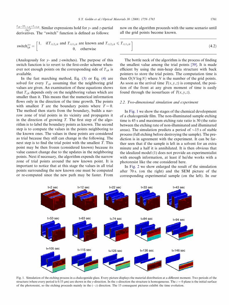
Fig. 1. Simulation of the etching process in a chalcogenide glass. Every picturestructure (where every period is 0.53 lm) are shown in the y-direction. In the x-dof the photoresist, so the etching proceeds mainly in the (�z) direction. The 1
now on the algorithm proceeds with the same scenario untilall the grid points become known.
The bottle neck of the algorithm is the process of findingthe smallest value among the trial points [39]. It is madeefficient by using the min-heap data structure with backpointers to store the trial points. The computation time isthen OðN log NÞ where N is the number of the grid points.As soon as the arrival time T(x,y,z) is computed, the posi-tion of the front at any given moment of time is easilyfound through the isosurfaces of T(x,y,z).
2.2. Two-dimensional simulation and experiment
In Fig. 1 we show the stages of the chemical developmentof a chalcogenide film. The non-illuminated sample etchingtime is 45 s and maximum etching rate ratio is 30 (the ratiobetween the etching rate of non-illuminated and illuminatedareas). The simulation predicts a period of �15 s of stableprocess (full etching before destroying the sample). The pre-diction is in agreement with the experiment. It can be far-ther seen that if the sample is left in a solvent for an extraminute and a half it is annihilated. It is then obvious thatthe idealized model (1) does not provide an experimentalistwith enough information, at least if he/she works with aphotoresist like the one considered here.
In Fig. 2 we show enlarged the result of the simulationafter 70 s. (on the right) and the SEM picture of thecorresponding experimental sample (on the left). In our
displays the material distribution at a different moment. Two periods of theirection the structure is homogeneous. The z = 0 plane is the initial surface5 consequent pictures exhibit the time evolution.

Fig. 2. On the right: the result of the simulation shown in Fig. 1 after 70 s. On the left: the SEM picture of the corresponding experimental sample. Bothpictures show approximately two periods of the structure (one period is 0.53 lm).
1762 S.Y. Goldin et al. / Optical Materials 30 (2008) 1759–1765
interference lithography writing system, an incoming laserbeam is split by a polarizing beam splitter into two equalbeams that form the arms of the interferometer with a sam-ple mounted at the point where the two arms cross. Using a532 nm CW frequency doubled Nd:YAG (COHERENTVERDI-5) laser, an induced photo-chemical change occurswithin the chalcogenide layer at each maximum of the inci-dent fringe pattern. An excellent agreement can be observedin this figure between the simulation and the experiment.
2.3. Three-dimensional simulation
The example brought in Fig. 3a–f shows etching of thephotonic crystal considered in Ref. [21]. Pictures a–f showthe time-development in the etching process. For this sim-ulation we assumed a sharp threshold speed-function. Dur-ing the three-dimensional etching process, the frontdevelops discontinuities and frequently different parts ofthe front merge. The chosen method proves to be able todeal perfectly with these problems.
3. Bi-continuity check and repair (removal of disconnected
regions)
The intensity distribution of the writing beams laserlight which defines the photonic crystal (1) is given by thefollowing function:
Ið�rÞ ¼ S0 þ 2S01 cosð�g1 � �r þ u01Þþ 2S02 cosð�g2 � �r þ u02Þþ 2S03 cosð�g3 � �r þ u03Þþ 2S12 cosðð�g2 � �g1Þ � �r þ u12Þþ 2S13 cosðð�g3 � �g1Þ � �r þ u13Þþ 2S23 cosðð�g3 � �g2Þ � �r þ u23Þ ð5Þ
Here �gi are defined by the differences between the wavevec-tors of the beams �ki: �gi ¼ �ki � �k0; while the other parame-
ters are determined by the directions, amplitudes andpolarization of the beams.
3.1. The method
The key observation is that the material is distributedaround the different maxima of the function Ið�rÞ. Indeed,if a maximum of Ið�rÞ is above the threshold there is necessar-ily a region around it where Ið�rÞ > I th, i.e. there is a lump ofmaterial around it. On the other hand, if a certain point,which is not a maximum, is above the threshold, one can‘‘start climbing” from this point to higher and higher Ið�rÞuntil he gets to a maximum ðIð�rÞ is clearly limited). There-fore, if all the maxima are connected the whole structure isconnected. If there is a disconnected region it belongs to acertain disconnected maximum. Similarly, the holes sur-round the minima. We then search for all the maxima andminima of Ið�rÞ, check their connections and delete the dis-connected regions. Hereafter we will talk about the maxima.
We accomplish our goals in four stages:(1) First, we find the maxima of Ið�rÞ. Since it is periodic
we have to search only in one primitive cell (one period) ofthe structure. We use a combination of the steepest descent(with fixed step) and Newton’s algorithms enriched with aspecial mechanism which takes care of the periodicity bybringing the point back as soon as it goes out of the prim-itive cell. This mechanism also helps us to get rid of artifi-cial maxima near the cell boundary.
(2) Second, we check if the maxima are directly con-nected. We look for the connections between different max-ima inside one primitive cell as well as between the 27neighboring cells. Fortunately, the defining intensity distri-bution Ið�rÞ is a fairly simple function (see formula (5)). Wethen assume that the connections between the lumps sur-rounding neighboring maxima include straight lines. Thisis frequently the case in the nature: if a couple of islandsin the sea are connected by a strap of dry land it usually

Fig. 3. Pictures (a)–(f) present the time-development in the etching process of a sample three-dimensional photonic crystal. Only three periods of thestructure are shown in every direction.
S.Y. Goldin et al. / Optical Materials 30 (2008) 1759–1765 1763
contains a straight or almost-straight line. Accordingly, welook for a minimum of Ið�rÞ on a straight path connecting apair of maxima and check if Ið�rÞ > I th in that point.
(3) Next, we check if the maxima are indirectly con-nected (through other maxima). Having chosen a certainorder of the maxima, we use the Floyd–Warshall algorithmfor finding the shortest path. The output shows how many‘‘links” (i.e. direct connections) it is necessary to follow to
get from one maximum to another. If the output matrix isfull of some numbers, the material is connected. If there arestill ‘‘infinity” entrances, it means that there are totally dis-connected maxima, so the material is disconnected.
(4) Finally, we eliminate the material around the isolatedmaxima (if they exist). In a numerical calculation the mate-rial and the air are represented by a matrix of e-values on agrid. The algorithm starts from the point of a maximum
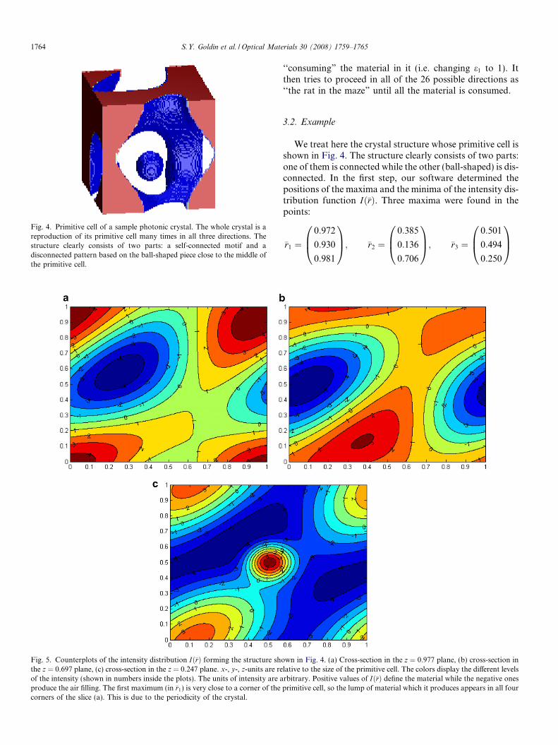
Fig. 4. Primitive cell of a sample photonic crystal. The whole crystal is areproduction of its primitive cell many times in all three directions. Thestructure clearly consists of two parts: a self-connected motif and adisconnected pattern based on the ball-shaped piece close to the middle ofthe primitive cell.
Fig. 5. Counterplots of the intensity distribution Ið�rÞ forming the structure shthe z = 0.697 plane, (c) cross-section in the z = 0.247 plane. x-, y-, z-units are reof the intensity (shown in numbers inside the plots). The units of intensity are aproduce the air filling. The first maximum (in �r1) is very close to a corner of thecorners of the slice (a). This is due to the periodicity of the crystal.
1764 S.Y. Goldin et al. / Optical Materials 30 (2008) 1759–1765
‘‘consuming” the material in it (i.e. changing e1 to 1). Itthen tries to proceed in all of the 26 possible directions as‘‘the rat in the maze” until all the material is consumed.
3.2. Example
We treat here the crystal structure whose primitive cell isshown in Fig. 4. The structure clearly consists of two parts:one of them is connected while the other (ball-shaped) is dis-connected. In the first step, our software determined thepositions of the maxima and the minima of the intensity dis-tribution function Ið�rÞ. Three maxima were found in thepoints:
�r1 ¼0:972
0:930
0:981
0B@
1CA; �r2 ¼
0:385
0:136
0:706
0B@
1CA; �r3 ¼
0:501
0:494
0:250
0B@
1CA
own in Fig. 4. (a) Cross-section in the z ¼ 0:977 plane, (b) cross-section inlative to the size of the primitive cell. The colors display the different levelsrbitrary. Positive values of Ið�rÞ define the material while the negative onesprimitive cell, so the lump of material which it produces appears in all four
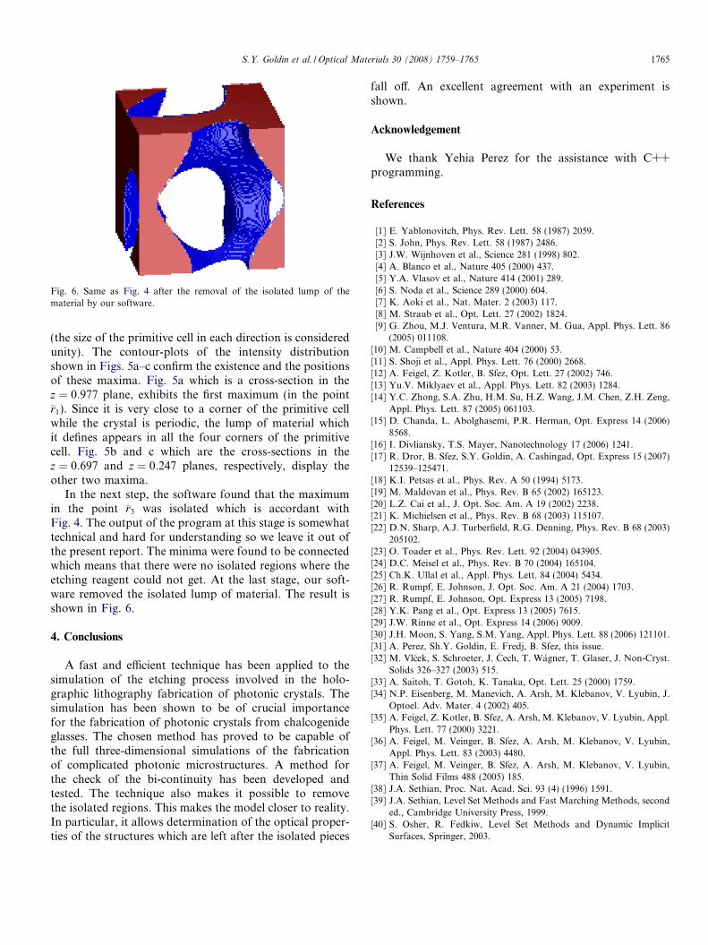
Fig. 6. Same as Fig. 4 after the removal of the isolated lump of thematerial by our software.
S.Y. Goldin et al. / Optical Materials 30 (2008) 1759–1765 1765
(the size of the primitive cell in each direction is consideredunity). The contour-plots of the intensity distributionshown in Figs. 5a–c confirm the existence and the positionsof these maxima. Fig. 5a which is a cross-section in thez ¼ 0:977 plane, exhibits the first maximum (in the point�r1). Since it is very close to a corner of the primitive cellwhile the crystal is periodic, the lump of material whichit defines appears in all the four corners of the primitivecell. Fig. 5b and c which are the cross-sections in thez ¼ 0:697 and z ¼ 0:247 planes, respectively, display theother two maxima.
In the next step, the software found that the maximumin the point �r3 was isolated which is accordant withFig. 4. The output of the program at this stage is somewhattechnical and hard for understanding so we leave it out ofthe present report. The minima were found to be connectedwhich means that there were no isolated regions where theetching reagent could not get. At the last stage, our soft-ware removed the isolated lump of material. The result isshown in Fig. 6.
4. Conclusions
A fast and efficient technique has been applied to thesimulation of the etching process involved in the holo-graphic lithography fabrication of photonic crystals. Thesimulation has been shown to be of crucial importancefor the fabrication of photonic crystals from chalcogenideglasses. The chosen method has proved to be capable ofthe full three-dimensional simulations of the fabricationof complicated photonic microstructures. A method forthe check of the bi-continuity has been developed andtested. The technique also makes it possible to removethe isolated regions. This makes the model closer to reality.In particular, it allows determination of the optical proper-ties of the structures which are left after the isolated pieces
fall off. An excellent agreement with an experiment isshown.
Acknowledgement
We thank Yehia Perez for the assistance with C++programming.
References
[1] E. Yablonovitch, Phys. Rev. Lett. 58 (1987) 2059.[2] S. John, Phys. Rev. Lett. 58 (1987) 2486.[3] J.W. Wijnhoven et al., Science 281 (1998) 802.[4] A. Blanco et al., Nature 405 (2000) 437.[5] Y.A. Vlasov et al., Nature 414 (2001) 289.[6] S. Noda et al., Science 289 (2000) 604.[7] K. Aoki et al., Nat. Mater. 2 (2003) 117.[8] M. Straub et al., Opt. Lett. 27 (2002) 1824.[9] G. Zhou, M.J. Ventura, M.R. Vanner, M. Gua, Appl. Phys. Lett. 86
(2005) 011108.[10] M. Campbell et al., Nature 404 (2000) 53.[11] S. Shoji et al., Appl. Phys. Lett. 76 (2000) 2668.[12] A. Feigel, Z. Kotler, B. Sfez, Opt. Lett. 27 (2002) 746.[13] Yu.V. Miklyaev et al., Appl. Phys. Lett. 82 (2003) 1284.[14] Y.C. Zhong, S.A. Zhu, H.M. Su, H.Z. Wang, J.M. Chen, Z.H. Zeng,
Appl. Phys. Lett. 87 (2005) 061103.[15] D. Chanda, L. Abolghasemi, P.R. Herman, Opt. Express 14 (2006)
8568.[16] I. Divliansky, T.S. Mayer, Nanotechnology 17 (2006) 1241.[17] R. Dror, B. Sfez, S.Y. Goldin, A. Cashingad, Opt. Express 15 (2007)
12539–125471.[18] K.I. Petsas et al., Phys. Rev. A 50 (1994) 5173.[19] M. Maldovan et al., Phys. Rev. B 65 (2002) 165123.[20] L.Z. Cai et al., J. Opt. Soc. Am. A 19 (2002) 2238.[21] K. Michielsen et al., Phys. Rev. B 68 (2003) 115107.[22] D.N. Sharp, A.J. Turberfield, R.G. Denning, Phys. Rev. B 68 (2003)
205102.[23] O. Toader et al., Phys. Rev. Lett. 92 (2004) 043905.[24] D.C. Meisel et al., Phys. Rev. B 70 (2004) 165104.[25] Ch.K. Ullal et al., Appl. Phys. Lett. 84 (2004) 5434.[26] R. Rumpf, E. Johnson, J. Opt. Soc. Am. A 21 (2004) 1703.[27] R. Rumpf, E. Johnson, Opt. Express 13 (2005) 7198.[28] Y.K. Pang et al., Opt. Express 13 (2005) 7615.[29] J.W. Rinne et al., Opt. Express 14 (2006) 9009.[30] J.H. Moon, S. Yang, S.M. Yang, Appl. Phys. Lett. 88 (2006) 121101.[31] A. Perez, Sh.Y. Goldin, E. Fredj, B. Sfez, this issue.[32] M. Vlcek, S. Schroeter, J. Cech, T. Wagner, T. Glaser, J. Non-Cryst.
Solids 326–327 (2003) 515.[33] A. Saitoh, T. Gotoh, K. Tanaka, Opt. Lett. 25 (2000) 1759.[34] N.P. Eisenberg, M. Manevich, A. Arsh, M. Klebanov, V. Lyubin, J.
Optoel. Adv. Mater. 4 (2002) 405.[35] A. Feigel, Z. Kotler, B. Sfez, A. Arsh, M. Klebanov, V. Lyubin, Appl.
Phys. Lett. 77 (2000) 3221.[36] A. Feigel, M. Veinger, B. Sfez, A. Arsh, M. Klebanov, V. Lyubin,
Appl. Phys. Lett. 83 (2003) 4480.[37] A. Feigel, M. Veinger, B. Sfez, A. Arsh, M. Klebanov, V. Lyubin,
Thin Solid Films 488 (2005) 185.[38] J.A. Sethian, Proc. Nat. Acad. Sci. 93 (4) (1996) 1591.[39] J.A. Sethian, Level Set Methods and Fast Marching Methods, second
ed., Cambridge University Press, 1999.[40] S. Osher, R. Fedkiw, Level Set Methods and Dynamic Implicit
Surfaces, Springer, 2003.
Copyright © 2022 FDOKUMEN