Infiltrated Photonic Crystal Fibers for Sensing Applications
Photonic crystal to photonic crystal surface modes: narrow-bandpass filters
Francisco Villa
Centro de Investigaciones en Optica, Loma del Bosque 115, Lomas del Campestre, León Gto 37150, Mexico [email protected]
J. A. Gaspar-Armenta Centro de Investigación en Física de la Universidad de Sonora. Apdo. Post. 5-088, Hermosillo Sonora 83190,
Mexico
Abstract: The properties of surface modes present in the junction of two different one-dimensional photonic crystals placed in series are studied to assess the possibility of applying them in the design of narrow-bandpass filters. To design bandpass filters that are similar in many respects to multiple-cavity Fabry–Perot filters, we also consider the coupling conditions for these surface modes for multiple photonic crystals placed in series to form a multiple-junction system.
© 2004 Optical Society of America
OCIS codes: (240.0240) Optics at surfaces; (310.0310) Thin films; (240.6690) Surface waves.
___________________________________________________________________________
References and Links
1. J. D. Joannopoulos, R. D. Meade, and J. N. Winn, Photonic Crystals: Molding the Flow of Light (Princeton University Press, Princeton, N.J., 1995).
2. S. Johnson and J. D. Joannopoulos, Photonic Crystals: the Road from Theory to Practice (Kluwer Academic Publishers, Boston 2002)
3. K. Sakoda, Optical Properties of Photonic Crystals (Springer Verlag, Heidelberg, 2001). 4. F. Ramos-Mendieta and P. Halevi, “Electromagnetic surface modes of a dielectric superlattice: the supercell
method,” J. Opt. Soc. Am. B 14 370–381 (1997). 5. B. Gralak, S. Ench, and G. Tayeb, "Anomalous refractive properties of photonic crystals," J. Opt. Soc. Am.
A 17 1012–1020 (2000). 6. F. Villa, L. E. Regalado, F. Ramos-Mendieta, J. Gaspar-Armenta, and T. López-Ríos, “Photonic crystal
sensor based on surface waves for thin film characterization,” Opt. Lett. 27 646–648 (2002). 7. J. Mizuguchi, Y. Tanaka, S. Tamura, and N. Notomi, "Focusing of light in a three dimensional cubic
photonic crystal," Phys. Rev. B 67, 075109 (2003). 8. F. Villa, J. A. Gaspar-Armenta, and F. Ramos-Mendieta, “One-dimensional photonic crystals: equivalent
systems to single layers with a classical oscillator like dielectric function,” Opt. Commun. 216 361–367 (2003).
9. Pochi Yeh, Amnon Yariv, and Chi-Shian Hong, “Electromagnetic propagation in periodic stratified media. I. General theory,” J. Opt. Soc. Am. 67, 423–438 (1977).
10. Pochi Yeh, Optical Waves in Layered Media (Wiley, New York, 1988). 11. W. M. Robertson and M. S. May, “Surface electromagnetic wave excitation on one-dimensional photonic
band-gap arrays,” Appl. Phys. Lett. 74 1800–1802 (1999). 12. W. M. Robertson, “Experimental measurement of the effect of termination on surface electromagnetic
waves in one-dimensional photonic bandgap arrays,” J. Lightwave Technol. 17 2013–2017 (1999). 13. F. Ramos-Mendieta and P. Halevi, "Surface electromagnetic waves in two-dimensional photonic crystals:
effect of the position of the surface plane," Phys. Rev. B 59 (1999) 15112–15120. 14. Xianmin Yi, Pochi Yeh, and John Hong, "Nonexistence of well-confined surface waves on obliquely cut
surfaces of one-dimensional photonic crystals," J. Opt. Soc. Am. B 18 (2001) 352–357. 15. Francisco Villa and J. A. Gaspar-Armenta, "Electromagnetic surface waves: photonic crystal-photonic
crystal interface," Opt. Commun. 223, 109–115 (2003). 16. Jorge A. Gaspar Armenta and Francisco Villa, “Photonic surface-wave excitation: photonic crystal-metal
interface,” J. Opt. Soc. Am. B 20, 2349–2354 (2003). 17. A. F. Turner, and P. W. Baumeister, "Multilayer mirrors with high reflectance over an extended spectral
region," Appl. Opt. 5, 69–76 (1966).
(C) 2004 OSA 31 May 2004 / Vol. 12, No. 11 / OPTICS EXPRESS 2338#3928 - $15.00 US Received 1 March 2004; revised 3 May 2004; accepted 5 May 2004
18. R. R. Austin, “Narrow band interference light filter,” U.S. Patent 3,528,726 (Sept. 15, 1970). 19. H. A. Macleod, Thin Film Optical Filters (McGraw Hill, New York, 1989). 20. C. J. Van der Laan and H. J. Franquena, “Equivalent layers: another way to look at them,” Appl. Opt. 34,
681–687 (1995). 21. J. A. Gaspar-Armenta, Francisco Villa, and T. López-Ríos,"Surface waves in finite one-dimensional
photonic crystals: mode coupling," Opt. Commun. 216 379–394 (2003). 22. H. A. Macleod, "Challenges in the design and production of narrow band filters for optical fiber
telecommunications," in Optical and Infrared Thin Films, Michael L. Fulton ed., Proc. SPIE 4094, 46–57 (2000).
_____________________________________________________________________________________________
1. Introduction
Photonic crystals have been an interesting field of intense research during the past years because of their potential to be applied in the development of all-optical circuits [1–3] and their interesting properties [4–7]. These systems, which constitute periodic arrays in one, two, and three dimensions of dielectric materials, present characteristic regions in the dispersion plane (frequency versus parallel component of the wave vector) that are called band structures, with bands where the light can propagate (the so-called bulk bands) and bands where light cannot propagate (bandgaps).
Although a photonic crystal represents an infinitely periodic system, in engineering applications they are finite or semi-infinite. When a photonic crystal is truncated, electromagnetic excitations can appear [8–14] at the surface of the photonic crystal in contact with any other bulk medium, such as a dielectric [4,8], a metal [16], or even another photonic crystal [15]. These surface modes are waves that propagate along the surface of the photonic crystal with evanescent fields in the perpendicular direction away from the surface plane, constituting a mechanism for energy loss—via tunneling—of localized bulk excitations.
When observed under reflectance or transmittance, surface modes appear as sharp troughs or peaks, respectively, that are similar to Fabry–Perot guided modes. Although Fabry–Perot filters are useful for solving many important design problems, these photonic-crystal–photonic-crystal bandpass filters deserve a detailed study to explore their properties and potential applications. It is worth mentioning that the knowledge of the existence of these modes is not new, since they were first mentioned by Turner and Baumeister [17], but they considered them more a nuisance than a potentially useful bandpass filter. Then Rusell and others in a patent [18] proposed the application of quarter-wave systems, calling them conjugated filters for reasons that we explain below. Unfortunately, no further studies were published about these systems.
Within this background, the present work proposes the study of other kinds of narrow-bandpass filters that present some advantages over the classical Fabry–Perot multiple-cavity filters. We call these filters multiple-junction photonic-crystal–photonic-crystal (MJPC-PC) filters because they are based on the excitation of surface modes by the coupling of different one-dimensional photonic crystals (1DPCs), as will become evident when the theory of such systems is considered.
2. Theory
In the formalism of the characteristic matrix method of propagation of light through multilayers [19], any simple thin film has an associated 2 × 2 matrix that relates the total electric and magnetic fields between the boundaries of one medium. This matrix is a function of only the parameters of the corresponding jth film:
=)cos()(
)()cos(),(
jjj
jj
jjj
sini
sini
mδδη
δη
δδη . (1)
(C) 2004 OSA 31 May 2004 / Vol. 12, No. 11 / OPTICS EXPRESS 2339#3928 - $15.00 US Received 1 March 2004; revised 3 May 2004; accepted 5 May 2004
It is worth mentioning that in the derivation of this matrix we are using the convention of a positive traveling wave ( )[ ]rktiEE �
���
⋅−= ωexp0 (in SI units), with ω being the angular
frequency, t the time, k�
the wave vector, and r� the position vector. Here
2j zj jk d
πδ =Λ
(2)
represents the phase thickness of the layer and jd its physical thickness;
2
/ TE polarization
/ TM polarization
zj
j
j zj
yk
yn k
ω
ωη =
(3)
stands for its optical admittance (the ratio of the total magnetic to electric fields, EH ), and
222 βω −= jzj nk (4)
is the wave vector’s reduced component perpendicular to interfaces. The constant y
represents the admittance of vacuum. Here cπωω 2/Λ= and πββ 2/Λ= represent the reduced frequency and the reduced parallel component of the wave vector, respectively. The arbitrary constant Λ has the same dimension as the thickness of layers, c is the speed of light
in vacuum, and jn is the refractive index of the medium.
It has been shown elsewhere [8, 19, 20] that a basic multilayer system of three layers that is symmetric with respect to a plane passing through its center of symmetry can be represented mathematically by a single equivalent layer that has an associated equivalent characteristic matrix,
( )
( ) ( )
cos sin( )( , )
sin cos
e eee e
e e e
i
M
i
δ δηη δ
η δ δ
=
, (5)
with a given equivalent phase thickness eδ and optical admittance eη . Considering the
symmetrical period of the three layers as the product ( ) ( ) ( )2/,,2/, ppqqpp mmm δηδηδη ,
we can determine the elements of the matrix:
11 cos( ) cos( ) sin( ) sin( )p q p qM δ δ ρ δ δ+= − , (6)
1122 MM = , (7)
21 [sin( ) cos( ) cos( ) sin( ) sin( )]p p q p q qM iη δ δ ρ δ δ ρ δ+ −= + − , (8)
12 sin( ) cos( ) cos( )sin( ) sin( )p q p q q
p
iM δ δ ρ δ δ ρ δ
η+ −= + + , (9)
where pη , qη represent the optical admittance of the layers of the period, pδ , qδ their
respective phase thickness, and
(C) 2004 OSA 31 May 2004 / Vol. 12, No. 11 / OPTICS EXPRESS 2340#3928 - $15.00 US Received 1 March 2004; revised 3 May 2004; accepted 5 May 2004
+=+
p
q
q
p
ηη
ηη
ρ2
1 , (10)
−=−
p
q
q
p
ηη
ηη
ρ2
1 . (11)
Although Eqs. (5) and (6)–(9) represent a mathematical equivalence, the equivalent functions eη , eδ are physically meaningful and allow us to consider a periodic system as though it were a single thin film with peculiar optical properties [8,10].
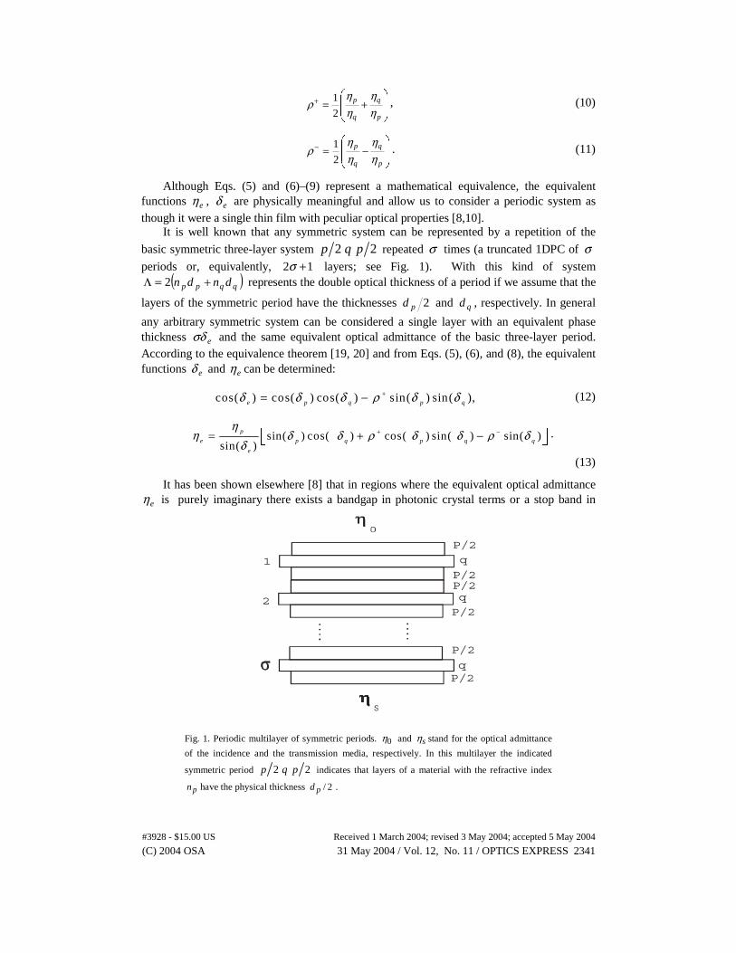
It is well known that any symmetric system can be represented by a repetition of the
basic symmetric three-layer system 2 2p q p repeated σ times (a truncated 1DPC of σ
periods or, equivalently, 12 +σ layers; see Fig. 1). With this kind of system ( )qqpp dndn +=Λ 2 represents the double optical thickness of a period if we assume that the
layers of the symmetric period have the thicknesses 2pd and qd , respectively. In general
any arbitrary symmetric system can be considered a single layer with an equivalent phase thickness eσδ and the same equivalent optical admittance of the basic three-layer period. According to the equivalence theorem [19, 20] and from Eqs. (5), (6), and (8), the equivalent functions eδ and eη can be determined:
cos( ) cos( ) cos( ) sin( ) sin( ),e p q p qδ δ δ ρ δ δ+= − (12)
sin( ) cos( ) cos( ) sin( ) sin( )sin( )
p
e p q p q q
e
ηη δ δ ρ δ δ ρ δ
δ+ −= + −
.
(13)
It has been shown elsewhere [8] that in regions where the equivalent optical admittance
eη is purely imaginary there exists a bandgap in photonic crystal terms or a stop band in
Fig. 1. Periodic multilayer of symmetric periods. 0η and sη stand for the optical admittance
of the incidence and the transmission media, respectively. In this multilayer the indicated
symmetric period 2 2p q p indicates that layers of a material with the refractive index
pn have the physical thickness 2/pd .
P/2q
P/2
P/2
P/2q
P/2
q
P/21
2
(C) 2004 OSA 31 May 2004 / Vol. 12, No. 11 / OPTICS EXPRESS 2341#3928 - $15.00 US Received 1 March 2004; revised 3 May 2004; accepted 5 May 2004
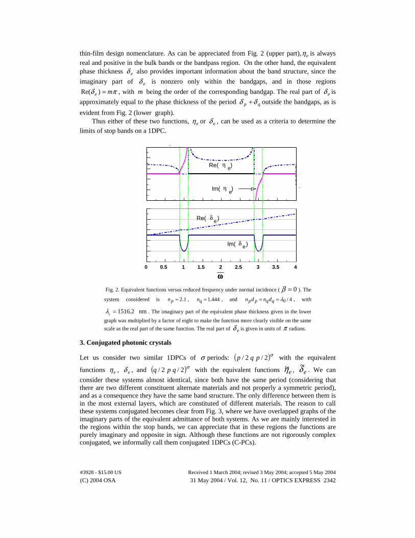
thin-film design nomenclature. As can be appreciated from Fig. 2 (upper part), eη is always real and positive in the bulk bands or the bandpass region. On the other hand, the equivalent phase thickness eδ also provides important information about the band structure, since the
imaginary part of eδ is nonzero only within the bandgaps, and in those regions
πδ me =)Re( , with m being the order of the corresponding bandgap. The real part of eδ is
approximately equal to the phase thickness of the period qp δδ + outside the bandgaps, as is
evident from Fig. 2 (lower graph). Thus either of these two functions, eη or eδ , can be used as a criteria to determine the
limits of stop bands on a 1DPC.
Fig. 2. Equivalent functions versus reduced frequency under normal incidence ( 0=β ). The
system considered is 1.2=pn , 444.1=qn , and 4/0λ== qqpp dndn , with
01516.2 nmλ = . The imaginary part of the equivalent phase thickness given in the lower
graph was multiplied by a factor of eight to make the function more clearly visible on the same
scale as the real part of the same function. The real part of eδ is given in units of π radians.
3. Conjugated photonic crystals
Let us consider two similar 1DPCs of σ periods: ( )σ2/2/ pqp with the equivalent
functions eη , eδ , and ( )σ2/2/ qpq with the equivalent functions eη~ , eδ~ . We can
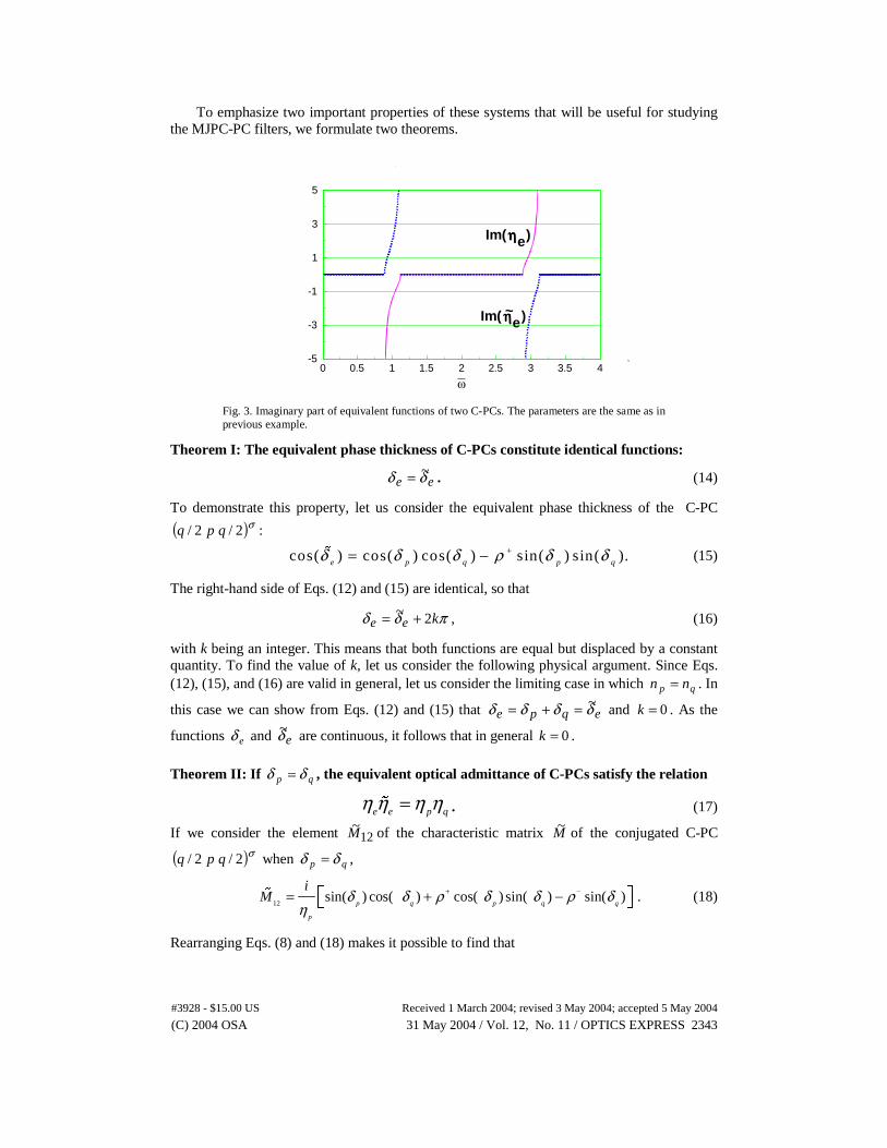
consider these systems almost identical, since both have the same period (considering that there are two different constituent alternate materials and not properly a symmetric period), and as a consequence they have the same band structure. The only difference between them is in the most external layers, which are constituted of different materials. The reason to call these systems conjugated becomes clear from Fig. 3, where we have overlapped graphs of the imaginary parts of the equivalent admittance of both systems. As we are mainly interested in the regions within the stop bands, we can appreciate that in these regions the functions are purely imaginary and opposite in sign. Although these functions are not rigorously complex conjugated, we informally call them conjugated 1DPCs (C-PCs).
0 0.5 1 1.5 2 2.5 3 3.5 4
ωωωω
Re( η )
Im( η )
e
e
e
e
Re( δ )
Im( δ )
(C) 2004 OSA 31 May 2004 / Vol. 12, No. 11 / OPTICS EXPRESS 2342#3928 - $15.00 US Received 1 March 2004; revised 3 May 2004; accepted 5 May 2004
To emphasize two important properties of these systems that will be useful for studying the MJPC-PC filters, we formulate two theorems.
Fig. 3. Imaginary part of equivalent functions of two C-PCs. The parameters are the same as in previous example.
Theorem I: The equivalent phase thickness of C-PCs constitute identical functions:
ee δδ ~= . (14)
To demonstrate this property, let us consider the equivalent phase thickness of the C-PC
( )σ2/2/ qpq :
cos( ) cos( ) cos( ) sin( ) sin( ).e p q p qδ δ δ ρ δ δ+= −� (15)
The right-hand side of Eqs. (12) and (15) are identical, so that
πδδ kee 2~ += , (16)
with k being an integer. This means that both functions are equal but displaced by a constant quantity. To find the value of k, let us consider the following physical argument. Since Eqs. (12), (15), and (16) are valid in general, let us consider the limiting case in which qp nn = . In
this case we can show from Eqs. (12) and (15) that eqpe δδδδ ~=+= and 0=k . As the
functions eδ and eδ~ are continuous, it follows that in general 0=k .
Theorem II: If qp δδ = , the equivalent optical admittance of C-PCs satisfy the relation
e e p qη η η η=� . (17)
If we consider the element 12~M of the characteristic matrix M~ of the conjugated C-PC
( )σ2/2/ qpq when qp δδ = ,
12sin( ) cos( ) cos( ) sin( ) sin( )
p q p q q
p
iM δ δ ρ δ δ ρ δ
η+ −= + −
� . (18)
Rearranging Eqs. (8) and (18) makes it possible to find that
0 0.5 1 1.5 2 2.5 3 3.5 4
ω
-5
-3
-1
1
3
5
Im( ηηηη )e
Im( ηηηη )e~
(C) 2004 OSA 31 May 2004 / Vol. 12, No. 11 / OPTICS EXPRESS 2343#3928 - $15.00 US Received 1 March 2004; revised 3 May 2004; accepted 5 May 2004
1221 ~M
Mq
pη
η= . (19)
Since, from Eq. (5),
21 sin( )e eM iη δ= , (20)
12 sin( )e
e
iM δ
η= ��
�
, (21)
by substituting Eqs. (20) and (21) into Eq. (19) and using Theorem I, we can derive Eq. (17).
4. Electromagnetic surface modes in conjugated photonic crystals
It is well known that, when a 1DPC is truncated, electromagnetic surface modes can appear within the bandgaps when the outermost periods are complete or incomplete [4, 8]. Let us consider an air–1DPC–C-PC system. For simplicity we are assuming that the 1DPC and C-PC are semi-infinite C-PCs, so if the number of periods of the C-PC goes to infinity ( ∞→σ~ ) we can consider the C-PC a bulk material; we are always in the spectral regions within the bandgaps. In this configuration the dispersion relation that determines the existence of surface modes will be given by
00 tan( ) 0e
e e e
e
iη η
η η η σδη
+ + + =
�
� , (22)
which results from assuming a null incident wave in the Fresnel reflection coefficient of the
system. In this equation 0η represents the optical admittance of the incidence medium.
Equation (22) is valid for any number of periods ( 2≥σ ), and it is useful to determine the surface modes of a finite truncated 1DPC that may be present on each one of its surfaces in
spite of its having only few periods. In this equation eη and eη� stand for the equivalent
optical admittance of the two different photonic crystals, and σ represents the number of periods of the 1DPC. When the phase thickness of the finite crystal goes to infinity ( ∞→σ ), Eq. (22) simplifies to the conditions
0ηη −=e , (23)
ee ηη ~−= . (24)
In this case Eq. (23) gives the condition for the existence of modes between the incidence medium and the 1DPC; if the incidence medium is a dielectric, this is a condition for the existence of the well-known photonic crystal–bulk dielectric surface modes [10–11]. Equation (24) establishes the condition for the existence of surface modes at the boundary 1DPC-C-PC. According to the analysis given elsewhere [15], the regions in which the optical admittances of the 1DPCs satisfy this condition lie within their corresponding bandgaps, so that the 1DPC-C-PC modes exist within the regions of overlapping bandgaps.
By means of the result of Theorem I and the condition that qp δδδ =≡ , the relation
given in Eq. (24) can be expressed as
(C) 2004 OSA 31 May 2004 / Vol. 12, No. 11 / OPTICS EXPRESS 2344#3928 - $15.00 US Received 1 March 2004; revised 3 May 2004; accepted 5 May 2004
2
)cos(
+−
=qp
qp
ηηηη
δ . (25)
This equation is valid even under nonnormal incidence. In the particular case in which both layers have the same quarter-wave optical thickness under normal incidence, it is customary to use the subscripts H (for a high-refractive-index layer) and L (for a low-index layer) instead of p and q. As Eq. (25) is independent of the order of the materials, it does not matter whether we take the basic period ( )2/2/ HLH or ( )2/2/ LHL ; the position of the
modes is unaltered. Since in this case 4/0λ== LLHH dndn ,
λλπδδδ 0
2==≡ LH , (26)
or
ωπδ2
= . (27)
Then, by substituting Eq. (26) into Eq. (25) and solving for the wavelength that denotes the position of the mode 1λ , we obtain
21
01
cos2
+−
=−
LH
LH
nn
nn
π
λλ . (28)
In this equation we used the subscript 1 for λ to indicate the bandgap number where the mode appears (first bandgap). It is worth mentioning that, since the argument of the cosine function is between zero and one, the denominator of Eq. (28) is less than (or equal to) unity;
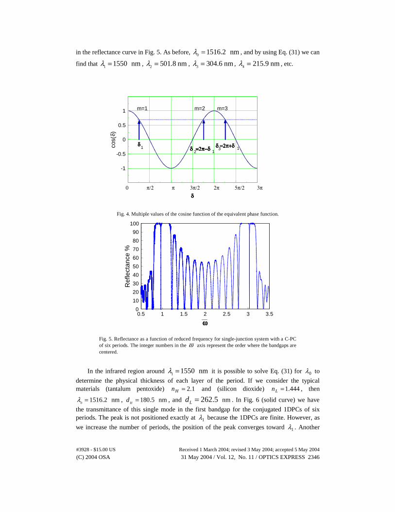
thus the wavelength where the mode appears, 1λ , is larger than the design wavelength, 0λ . Equation (25) is multivalued in wavelength (or frequency). With the help of Fig. 4 it is
possible to find a relation to determine the phase values corresponding to the position of modes at the subsequent bandgaps:
( )[ ] ( ) 112
112 δπδ mmm m −−−+−= , (29)
where 1, 2,m = … represents the order of the bandgap. By definition mδ represents the
phase thickness at various wavelengths where the modes appear:
m
m λλπδ 0
2= . (30)
Therefore, from Eqs. (28) and (30), the general relation that determines the position of the modes will be
21
0
cos2
)1()1(12
+−
−−−+−
=−
LH
LHmm
m
nn
nnm
π
λλ . (31)
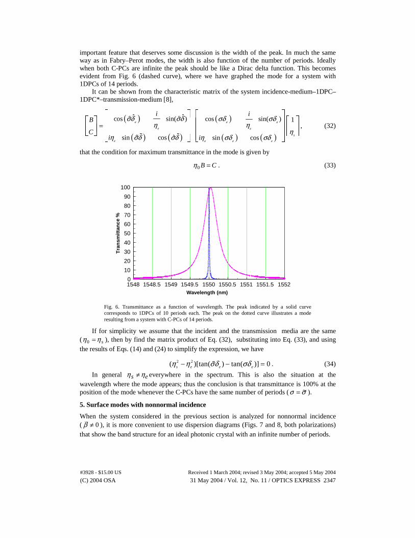
Considering the conjugated systems of Figs. (2) and (3) with nine periods each, joined to
form the PC–PC junction, it is possible to see the modes as dips in the regions of stop bands
(C) 2004 OSA 31 May 2004 / Vol. 12, No. 11 / OPTICS EXPRESS 2345#3928 - $15.00 US Received 1 March 2004; revised 3 May 2004; accepted 5 May 2004
in the reflectance curve in Fig. 5. As before, 0 1516.2 nmλ = , and by using Eq. (31) we can
find that 1 1550 nmλ = , 2 501.8 nmλ = , 3 304.6 nmλ = , 4 215.9 nmλ = , etc.
Fig. 4. Multiple values of the cosine function of the equivalent phase function.
Fig. 5. Reflectance as a function of reduced frequency for single-junction system with a C-PC of six periods. The integer numbers in the ω axis represent the order where the bandgaps are centered.
In the infrared region around 1 1550 nmλ = it is possible to solve Eq. (31) for 0λ to
determine the physical thickness of each layer of the period. If we consider the typical materials (tantalum pentoxide) 1.2=Hn and (silicon dioxide) 444.1=Ln , then
01516.2 nmλ = , 180.5 nm
Hd = , and nm262.5Ld = . In Fig. 6 (solid curve) we have
the transmittance of this single mode in the first bandgap for the conjugated 1DPCs of six periods. The peak is not positioned exactly at 1λ because the 1DPCs are finite. However, as
we increase the number of periods, the position of the peak converges toward 1λ . Another
0.5 1 1.5 2 2.5 3 3.5
ωωωω
0
10
20
30
40
50
60
70
80
90
100
Ref
lect
ance
%
δδδδ
-1
-0.5
0
0.5
1co
s(δ )
0 π/2 π 3π/2 2π 5π/2 3π
m=1 m=2 m=3
δδδδδ =2π−δδ =2π−δδ =2π−δδ =2π−δ δ =2π+δδ =2π+δδ =2π+δδ =2π+δ
21
113
(C) 2004 OSA 31 May 2004 / Vol. 12, No. 11 / OPTICS EXPRESS 2346#3928 - $15.00 US Received 1 March 2004; revised 3 May 2004; accepted 5 May 2004
important feature that deserves some discussion is the width of the peak. In much the same way as in Fabry–Perot modes, the width is also function of the number of periods. Ideally when both C-PCs are infinite the peak should be like a Dirac delta function. This becomes evident from Fig. 6 (dashed curve), where we have graphed the mode for a system with 1DPCs of 14 periods.
It can be shown from the characteristic matrix of the system incidence-medium–1DPC–1DPC*–transmission-medium [8],
( )
( ) ( )
( )
( ) ( )
cos sin( ) cos sin( ) 1
sin cos sin cos
e e e
e e
s
e e e e
i iB
Ci i
σδ σδ σδ σδη η
ηη σδ σδ η σδ σδ
=
� �
� �
� �
� �
, (32)
that the condition for maximum transmittance in the mode is given by
CB =0η . (33)
Fig. 6. Transmittance as a function of wavelength. The peak indicated by a solid curve corresponds to 1DPCs of 10 periods each. The peak on the dotted curve illustrates a mode resulting from a system with C-PCs of 14 periods.
If for simplicity we assume that the incident and the transmission media are the same ( sηη =0 ), then by find the matrix product of Eq. (32), substituting into Eq. (33), and using the results of Eqs. (14) and (24) to simplify the expression, we have
2 2( )[tan( ) tan( )] 0s e e eη η σδ σδ− − =� . (34)
In general es ηη ≠ everywhere in the spectrum. This is also the situation at the wavelength where the mode appears; thus the conclusion is that transmittance is 100% at the position of the mode whenever the C-PCs have the same number of periods ( σσ ~= ).
5. Surface modes with nonnormal incidence
When the system considered in the previous section is analyzed for nonnormal incidence ( 0≠β ), it is more convenient to use dispersion diagrams (Figs. 7 and 8, both polarizations) that show the band structure for an ideal photonic crystal with an infinite number of periods.
1548 1548.5 1549 1549.5 1550 1550.5 1551 1551.5 1552Wavelength (nm)
0
10
20
30
40
50
60
70
80
90
100
Tra
nsm
itta
nce
%
(C) 2004 OSA 31 May 2004 / Vol. 12, No. 11 / OPTICS EXPRESS 2347#3928 - $15.00 US Received 1 March 2004; revised 3 May 2004; accepted 5 May 2004
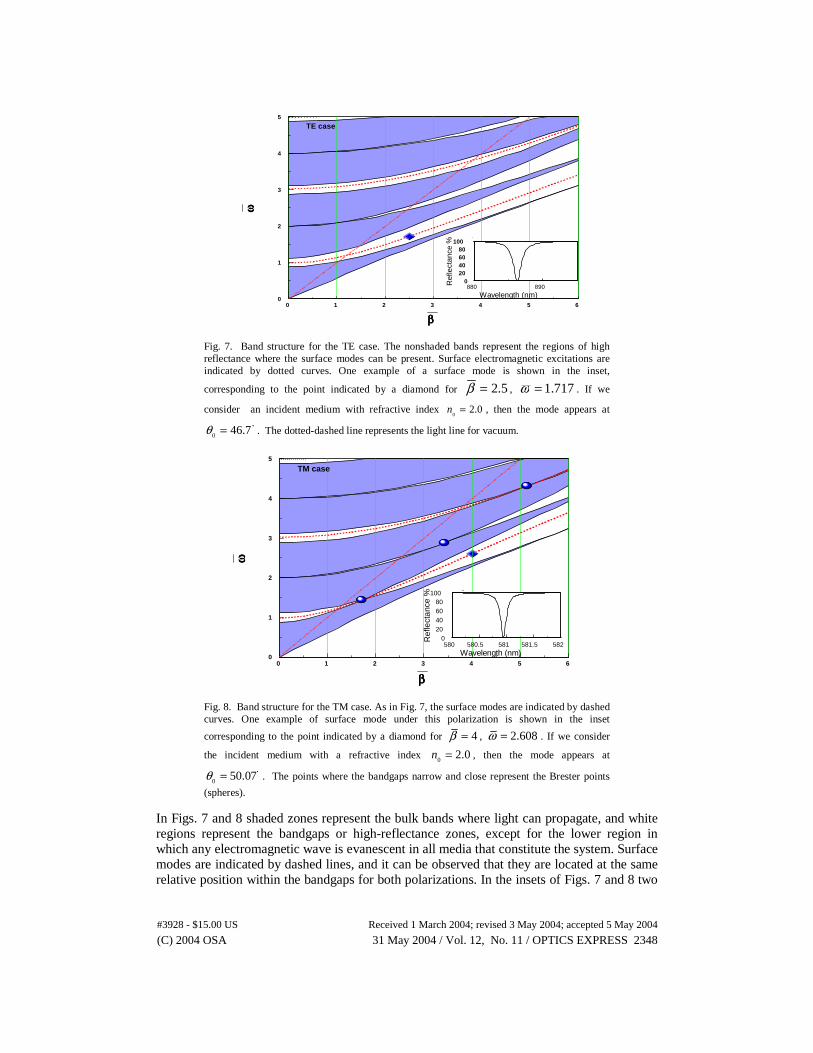
Fig. 7. Band structure for the TE case. The nonshaded bands represent the regions of high reflectance where the surface modes can be present. Surface electromagnetic excitations are indicated by dotted curves. One example of a surface mode is shown in the inset,
corresponding to the point indicated by a diamond for 2.5β = , 717.1=ω . If we
consider an incident medium with refractive index 0
2.0n = , then the mode appears at
046.7θ = �
. The dotted-dashed line represents the light line for vacuum.
Fig. 8. Band structure for the TM case. As in Fig. 7, the surface modes are indicated by dashed curves. One example of surface mode under this polarization is shown in the inset
corresponding to the point indicated by a diamond for 4β = , 2.608ω = . If we consider
the incident medium with a refractive index 0
2.0n = , then the mode appears at
050.07θ = �
. The points where the bandgaps narrow and close represent the Brester points
(spheres).
In Figs. 7 and 8 shaded zones represent the bulk bands where light can propagate, and white regions represent the bandgaps or high-reflectance zones, except for the lower region in which any electromagnetic wave is evanescent in all media that constitute the system. Surface modes are indicated by dashed lines, and it can be observed that they are located at the same relative position within the bandgaps for both polarizations. In the insets of Figs. 7 and 8 two
0 1 2 3 4 5 6
ββββ
0
1
2
3
4
5
ωω ωω
880 890
Wavelength (nm)
020406080
100
Ref
lect
ance
%
TE case
0 1 2 3 4 5 6
ββββ
0
1
2
3
4
5
ωω ωω
580 580.5 581 581.5 582Wavelength (nm)
020406080
100
Ref
lect
anc
e %
TM case
(C) 2004 OSA 31 May 2004 / Vol. 12, No. 11 / OPTICS EXPRESS 2348#3928 - $15.00 US Received 1 March 2004; revised 3 May 2004; accepted 5 May 2004
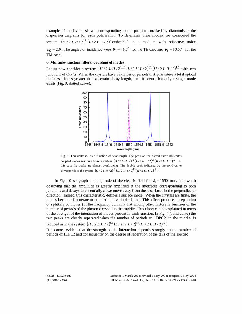
example of modes are shown, corresponding to the positions marked by diamonds in the dispersion diagrams for each polarization. To determine these modes, we considered the
system ( ) ( )33 2/2/2/2/ LHLHLH embedded in a medium with refractive index
0.20 =n . The angles of incidence were �7.46=iθ for the TE case and �07.50=iθ for the TM case.
6. Multiple-junction filters: coupling of modes
Let us now consider a system ( ) ( ) ( )122512 2/2/2/2/2/2/ HLHLHLHLH with two junctions of C-PCs. When the crystals have a number of periods that guarantees a total optical thickness that is greater than a certain decay length, then it seems that only a single mode exists (Fig. 9, dotted curve).
Fig. 9. Transmittance as a function of wavelength. The peak on the dotted curve illustrates
coupled modes resulting from a system ( ) ( ) ( )122512 2/2/2/2/2/2/ HLHLHLHLH . In
this case the peaks are almost overlapping. The double peak indicated by the solid curve
corresponds to the system ( ) ( ) ( )121512 2/2/2/2/2/2/ HLHLHLHLH .
In Fig. 10 we graph the amplitude of the electric field for 1 1550 nmλ = . It is worth
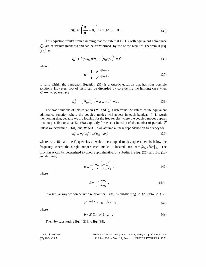
observing that the amplitude is greatly amplified at the interfaces corresponding to both junctions and decays exponentially as we move away from these surfaces in the perpendicular direction. Indeed, this characteristic, defines a surface mode. When the crystals are finite, the modes become degenerate or coupled to a variable degree. This effect produces a separation or splitting of modes (in the frequency domain) that among other factors is function of the number of periods of the photonic crystal in the middle. This effect can be explained in terms of the strength of the interaction of modes present in each junction. In Fig. 7 (solid curve) the two peaks are clearly separated when the number of periods of 1DPC2, in the middle, is
reduced as in the system ( ) ( ) ( )121512 2/2/2/2/2/2/ HLHLHLHLH . It becomes evident that the strength of the interaction depends strongly on the number of periods of 1DPC2 and consequently on the degree of separation of the tails of the electric
1548 1548.5 1549 1549.5 1550 1550.5 1551 1551.5 1552Wavelength (nm)
0
10
20
30
40
50
60
70
80
90
100
Tra
nsm
itta
nce
%
(C) 2004 OSA 31 May 2004 / Vol. 12, No. 11 / OPTICS EXPRESS 2349#3928 - $15.00 US Received 1 March 2004; revised 3 May 2004; accepted 5 May 2004
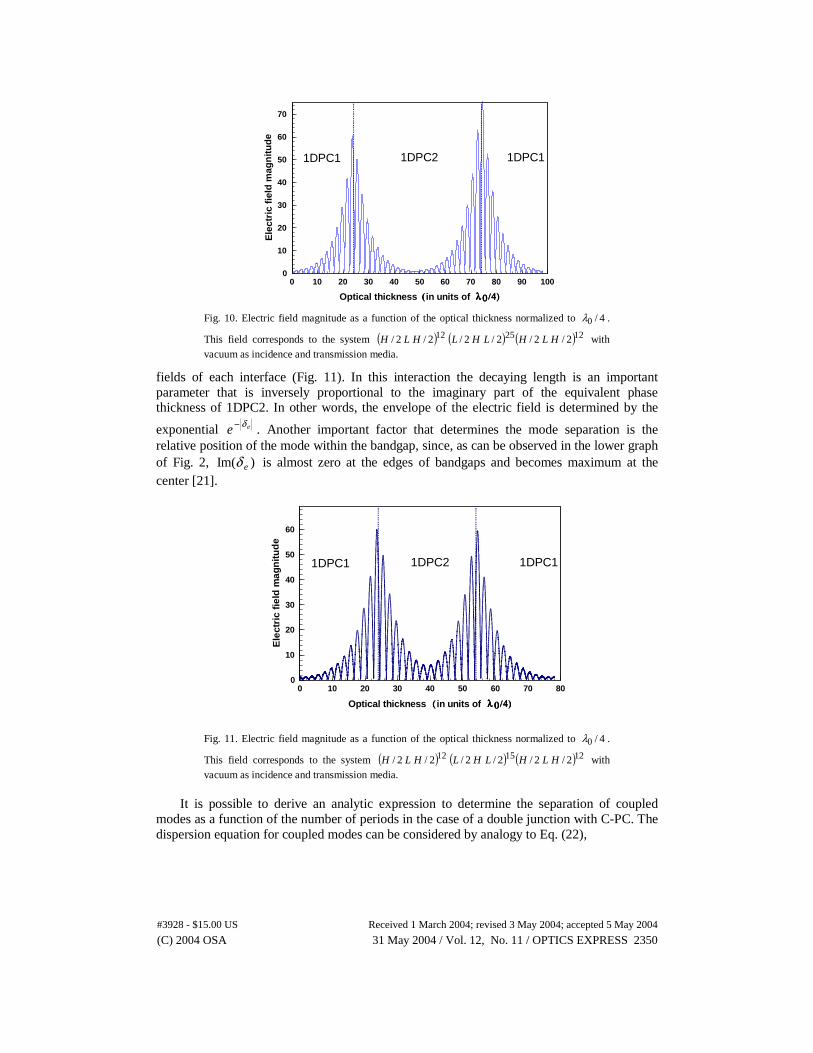
Fig. 10. Electric field magnitude as a function of the optical thickness normalized to 4/0λ .
This field corresponds to the system ( ) ( ) ( )122512 2/2/2/2/2/2/ HLHLHLHLH with vacuum as incidence and transmission media.
fields of each interface (Fig. 11). In this interaction the decaying length is an important parameter that is inversely proportional to the imaginary part of the equivalent phase thickness of 1DPC2. In other words, the envelope of the electric field is determined by the
exponential ee δ− . Another important factor that determines the mode separation is the relative position of the mode within the bandgap, since, as can be observed in the lower graph of Fig. 2, )Im( eδ is almost zero at the edges of bandgaps and becomes maximum at the center [21].
Fig. 11. Electric field magnitude as a function of the optical thickness normalized to 4/0λ .
This field corresponds to the system ( ) ( ) ( )121512 2/2/2/2/2/2/ HLHLHLHLH with vacuum as incidence and transmission media.
It is possible to derive an analytic expression to determine the separation of coupled
modes as a function of the number of periods in the case of a double junction with C-PC. The dispersion equation for coupled modes can be considered by analogy to Eq. (22),
0 10 20 30 40 50 60 70 80 90 100
Optical thickness ( ( ( ( in units of λ λ λ λ 0000 /4)/4)/4)/4)
0
10
20
30
40
50
60
70
Ele
ctri
c fi
eld
mag
nit
ud
e
1DPC1 1DPC2 1DPC1
0 10 20 30 40 50 60 70 80
Optical thickness ( ( ( ( in units of λ λ λ λ 0000 /4)/4)/4)/4)
0
10
20
30
40
50
60
Ele
ctri
c fi
eld
mag
nit
ud
e
1DPC1 1DPC2 1DPC1
(C) 2004 OSA 31 May 2004 / Vol. 12, No. 11 / OPTICS EXPRESS 2350#3928 - $15.00 US Received 1 March 2004; revised 3 May 2004; accepted 5 May 2004
2
2 tan( ) 0ee e e
e
iηη η σδη
+ + =
�
� . (35)
This equation results from assuming that the external C-PCs with equivalent admittance
eη~ are of infinite thickness and can be transformed, by use of the result of Theorem II [Eq.
(17)], to
( ) 02 224 =++ LHeLHe a ηηηηηη , (36)
where
)Im(
)Im(
1
1e
e
e
ea
δσ
δσ
−
−
−+= (37)
is valid within the bandgaps. Equation (36) is a quartic equation that has four possible solutions. However, two of them can be discarded by considering the limiting case when
∞→σ , so we have
12 −±−=± aaLHe ηηη . (38)
The two solutions of this equation ( +eη and −
eη ) determine the values of the equivalent admittance function where the coupled modes will appear in each bandgap. It is worth mentioning that, because we are looking for the frequencies where the coupled modes appear, it is not possible to solve Eq. (38) explicitly for ω as a function of the number of periods σ
unless we determine )(ωδ e and )(ωη ±e . If we assume a linear dependence on frequency for
)()( 11 ωωαωηη −+≅ ±±
ee , (39)
where +ω , −ω are the frequencies at which the coupled modes appear, 1ω is below the
frequency where the single nonperturbed mode is located, and [ ]1
/ ωωηα ∂∂= e . The
function α can be determined to good approximation by substituting Eq. (25) into Eq. (13) and deriving
( )( )∆+
∆+∆
≅1
1
2
22Hi
ηπα , (40)
where
LH
LH
ηηηη
+−
=∆ . (41)
In a similar way we can derive a relation for )(ωδ e by substituting Eq. (25) into Eq. (12),
12)Im( −−−≅− bbe eδ , (42)
where ++ −+∆= ρρ )1(4b . (43)
Then, by substituting Eq. (42) into Eq. (38),
(C) 2004 OSA 31 May 2004 / Vol. 12, No. 11 / OPTICS EXPRESS 2351#3928 - $15.00 US Received 1 March 2004; revised 3 May 2004; accepted 5 May 2004
11
112
2
−++
−−−=bb
bba . (44)
So, with Eq. (44), the solutions for ±eη in Eq. (38) can be determined explicitly. Finally,
if we solve Eqs. (39) for +ω and −ω ,
−+
−+
±+−
±≅ee
ee
ηηηηωω 1 . (45)
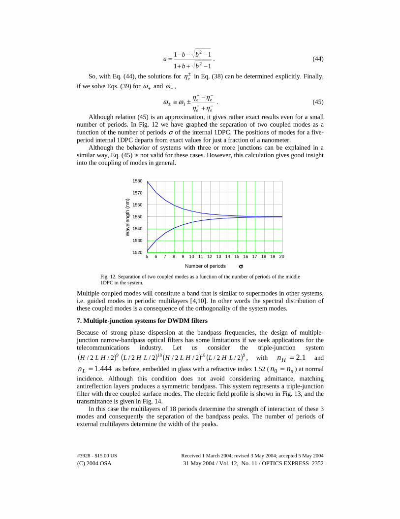
Although relation (45) is an approximation, it gives rather exact results even for a small number of periods. In Fig. 12 we have graphed the separation of two coupled modes as a function of the number of periods σ of the internal 1DPC. The positions of modes for a five-period internal 1DPC departs from exact values for just a fraction of a nanometer.
Although the behavior of systems with three or more junctions can be explained in a similar way, Eq. (45) is not valid for these cases. However, this calculation gives good insight into the coupling of modes in general.
Fig. 12. Separation of two coupled modes as a function of the number of periods of the middle 1DPC in the system.
Multiple coupled modes will constitute a band that is similar to supermodes in other systems, i.e. guided modes in periodic multilayers [4,10]. In other words the spectral distribution of these coupled modes is a consequence of the orthogonality of the system modes.
7. Multiple-junction systems for DWDM filters
Because of strong phase dispersion at the bandpass frequencies, the design of multiple-junction narrow-bandpass optical filters has some limitations if we seek applications for the telecommunications industry. Let us consider the triple-junction system
( ) ( ) ( ) ( )918189 2/2/2/2/2/2/2/2/ LHLHLHLHLHLH , with 1.2=Hn and
444.1=Ln as before, embedded in glass with a refractive index 1.52 ( snn =0 ) at normal
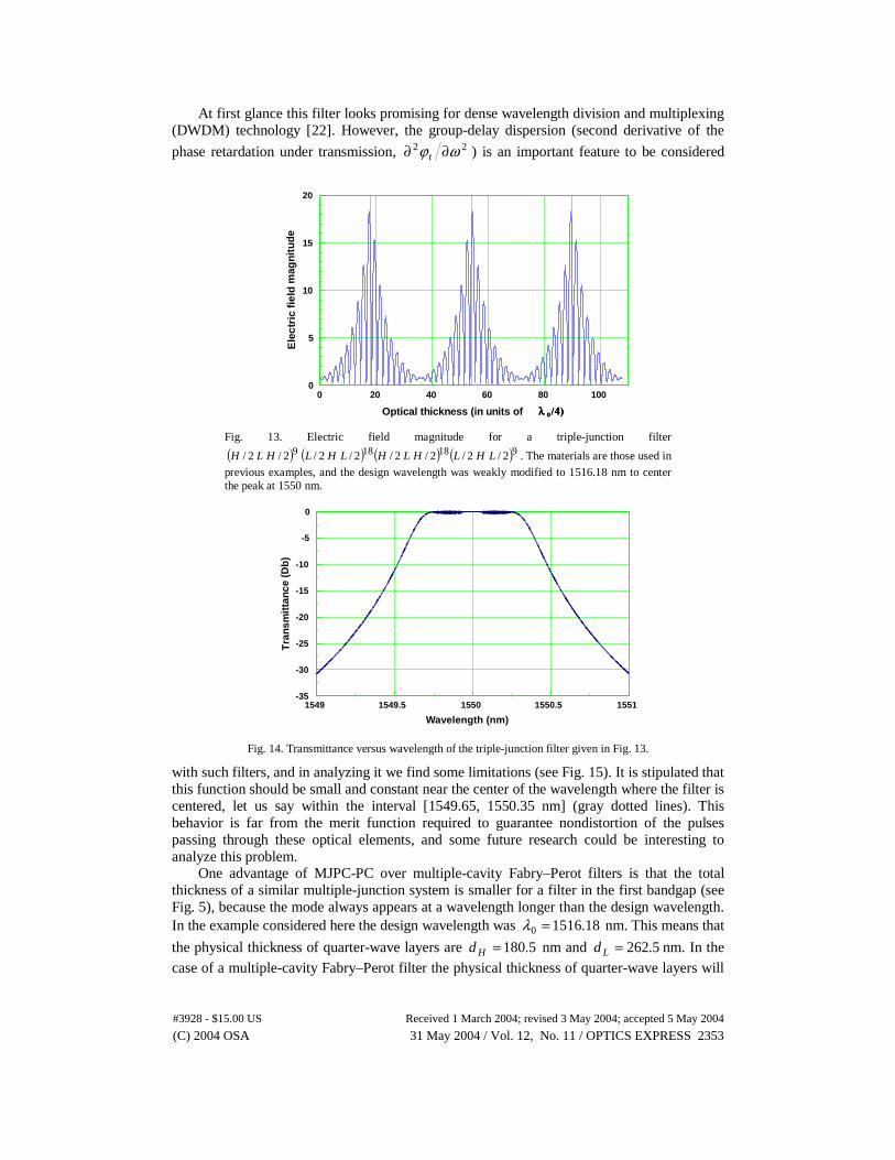
incidence. Although this condition does not avoid considering admittance, matching antireflection layers produces a symmetric bandpass. This system represents a triple-junction filter with three coupled surface modes. The electric field profile is shown in Fig. 13, and the transmittance is given in Fig. 14.
In this case the multilayers of 18 periods determine the strength of interaction of these 3 modes and consequently the separation of the bandpass peaks. The number of periods of external multilayers determine the width of the peaks.
5 6 7 8 9 10 11 12 13 14 15 16 17 18 19 20
Number of periods σσσσ
1520
1530
1540
1550
1560
1570
1580
Wav
elen
gth
(nm
)
(C) 2004 OSA 31 May 2004 / Vol. 12, No. 11 / OPTICS EXPRESS 2352#3928 - $15.00 US Received 1 March 2004; revised 3 May 2004; accepted 5 May 2004
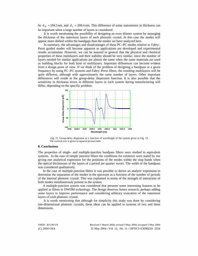
At first glance this filter looks promising for dense wavelength division and multiplexing (DWDM) technology [22]. However, the group-delay dispersion (second derivative of the
phase retardation under transmission, 22 ωϕ ∂∂ t ) is an important feature to be considered
Fig. 13. Electric field magnitude for a triple-junction filter
( ) ( ) ( ) ( )918189 2/2/2/2/2/2/2/2/ LHLHLHLHLHLH . The materials are those used in previous examples, and the design wavelength was weakly modified to 1516.18 nm to center the peak at 1550 nm.
Fig. 14. Transmittance versus wavelength of the triple-junction filter given in Fig. 13.
with such filters, and in analyzing it we find some limitations (see Fig. 15). It is stipulated that this function should be small and constant near the center of the wavelength where the filter is centered, let us say within the interval [1549.65, 1550.35 nm] (gray dotted lines). This behavior is far from the merit function required to guarantee nondistortion of the pulses passing through these optical elements, and some future research could be interesting to analyze this problem.
One advantage of MJPC-PC over multiple-cavity Fabry–Perot filters is that the total thickness of a similar multiple-junction system is smaller for a filter in the first bandgap (see Fig. 5), because the mode always appears at a wavelength longer than the design wavelength. In the example considered here the design wavelength was 18.15160 =λ nm. This means that
the physical thickness of quarter-wave layers are 5.180=Hd nm and 5.262=Ld nm. In the case of a multiple-cavity Fabry–Perot filter the physical thickness of quarter-wave layers will
0 20 40 60 80 100
Optical thickness (in units of λ λ λ λ 0000 /4)/4)/4)/4)
0
5
10
15
20
Ele
ctri
c fi
eld
mag
nit
ud
e
1549 1549.5 1550 1550.5 1551
Wavelength (nm)
-35
-30
-25
-20
-15
-10
-5
0
Tra
nsm
itta
nce
(Db
)
(C) 2004 OSA 31 May 2004 / Vol. 12, No. 11 / OPTICS EXPRESS 2353#3928 - $15.00 US Received 1 March 2004; revised 3 May 2004; accepted 5 May 2004
be 5.184=Hd nm, and 4.268=Ld nm. This difference of some nanometers in thickness can be important when a large number of layers is considered.
It is worth mentioning the possibility of designing an even thinner system by managing the thickness of the outermost layers of each photonic crystal. In this case the modes will appear more shifted within the bandgaps than the modes we have analyzed here.
In summary, the advantages and disadvantages of these PC–PC modes relative to Fabry–Perot guided modes will become apparent as applications are developed and experimental results accumulate. However, we can be assured in general that the physical and chemical properties of these multilayers and their stability should be very similar, since the number of layers needed for similar applications are almost the same when the same materials are used as building blocks for both kind of multilayers. Important differences can become evident from a design point of view. If we think of the problem of designing a bandpass at a given frequency by using PC–PC systems and Fabry–Perot filters, the resulting multilayers will be quite different, although with approximately the same number of layers. Other important differences will reside in the group-delay dispersion function. It is also possible that the sensitivity to thickness errors in different layers in each system during manufacturing will differ, depending on the specific problem.
Fig. 15. Group-delay dispersion as a function of wavelength of the system given in Fig. 13. The vertical axis is given in squared picoseconds.
8. Conclusions
The properties of single- and multiple-junction bandpass filters were studied in equivalent systems. In the case of simple junction filters the conditions for existence were stated by our giving one analytical expression for the positions of the modes within the stop bands when the optical thicknesses of the layers of a period are quarter waves. The width of the bandpass was considered qualitatively. In the case of multiple-junction filters it was possible to derive an analytic expression to determine the separation of the modes in the spectrum as a function of the number of periods of the internal photonic crystal. This was explained in terms of the strength of interaction of both modes simultaneously present in the system. A multiple-junction system was considered that presents some interesting features to be applied as filters in DWDM technology. The design deserves future research, perhaps adding some layers to improve performance and considering arbitrary truncation of the outermost layers of each photonic crystal. It is worth mentioning that although for simplicity this study was done by considering one-dimensional photonic crystals, these ideas can be applied to systems of two and three dimensions.
1548 1548.5 1549 1549.5 1550 1550.5 1551 1551.5 1552
Wavelength (nm)
-100
-50
0
50
100
Gro
up
del
ay d
isp
ersi
on
(p
s2)
(C) 2004 OSA 31 May 2004 / Vol. 12, No. 11 / OPTICS EXPRESS 2354#3928 - $15.00 US Received 1 March 2004; revised 3 May 2004; accepted 5 May 2004

Acknowledgments
We appreciate the valuable comments of professor H. A. Macleod.
(C) 2004 OSA 31 May 2004 / Vol. 12, No. 11 / OPTICS EXPRESS 2355#3928 - $15.00 US Received 1 March 2004; revised 3 May 2004; accepted 5 May 2004
Copyright © 2022 FDOKUMEN