Method to map individual electromagnetic field components inside a photonic crystal
12
Mapping individual electromagnetic field components inside a photonic crystal T. Denis, 1,* B. Reijnders, 1 J. H. H. Lee, 1 P. J. M. van der Slot, 1 W. L. Vos, 2 and K.-J. Boller 1 1 Laser Physics and Nonlinear Optics, MESA+ Institute for Nanotechnology, University of Twente, P.O.Box 217, 7500 AE Enschede, The Netherlands 2 Complex Photonic Systems (COPS), MESA+ Institute for Nanotechnology, University of Twente, P.O.Box 217, 7500 AE Enschede, The Netherlands *[email protected] Abstract: We present a method to map the absolute electromagnetic field strength inside photonic crystals. We apply the method to map the electric field component E z of a two-dimensional photonic crystal slab at microwave frequencies. The slab is placed between two mirrors to select Bloch standing waves and a subwavelength spherical scatterer is scanned inside the resulting resonator. The resonant Bloch frequencies shift depending on the electric field at the position of the scatterer. To map the electric field component E z we measure the frequency shift in the reflection and transmission spectrum of the slab versus the scatterer position. Very good agreement is found between measurements and calculations without any adjustable parameters. © 2012 Optical Society of America OCIS codes: (350.4238) Nanophotonics and photonic crystals; (050.5298) Photonic crystals; (160.5293) Photonic bandgap materials; (160.5298) Photonic crystals; (230.5298) Photonic crystals. References and links 1. S. John, “Strong localization of photons in certain disordered dielectric superlattices,” Phys. Rev. Lett. 58, 2486– 2489 (1987). 2. E. Yablonovitch, “Inhibited spontaneous emission in solid-state physics and electronics,” Phys. Rev. Lett. 58, 2059–2062 (1987). 3. J. D. Joannopoulos, S. G. Johnson, J. N. Winn, and R. D. Meade, Photonic crystals: molding the flow of light (Princeton University Press, 2008). 4. N. W. Ashcroft and N. D. Mermin, Solid state physics (Holt, Rinehard & Winston, 1976). 5. R. Sprik, B. A. van Tiggelen, and A. Lagendijk, “Optical emission in periodic dielectrics,” Europhys. Lett. 35, 265–270 (1996). 6. P. Lodahl, A. F. van Driel, I. S. Nikolaev, A. Irman, K. Overgang, D. Vanmaekelbergh, and W. L. Vos, “Con- trolling the dynamics of spontaneous emission from quantum dots by photonic crystals,” Nature 430, 654–657 (2004). 7. M. Fujita, S. Takahashi, Y. Tanaka, T. Asano, and S. Noda, “Simultaneous inhibition and redistribution of spon- taneous light emission in photonic crystals,” Science 308, 1296–1298 (2005). 8. H. Caglayan, I. Bulu, and E. Ozbay, “Highly directional enhanced radiation from sources embedded inside three- dimensional photonic crystals,” Opt. Express 13, 7645–7652 (2005). 9. A. F. Koenderink, M. Kafesaki, C. M. Soukoulis, and V. Sandoghdar, “Spontaneous emission in the near-field of two-dimensional photonic crystals,” Opt. Lett. 30, 3210–3212 (2005). 10. A. Rodenas, G. Zhou, D. Jaque, and M. Gu, “Rare-earth spontaneous emission control in three-dimensional lithium niobate photonic crystals,” Adv. Mater. 21, 3526-3530 (2009). 11. L. Sapienza, H. Thyrrestrup, S. Stobbe, P. D. Garcia, S. Smolka, and P. Lodahl, “Cavity quantum electrodynamics with Anderson-localized modes,” Science 327, 1352–1355 (2010). 1 arXiv:1207.2004v1 [physics.optics] 9 Jul 2012
Transcript of Method to map individual electromagnetic field components inside a photonic crystal
Mapping individual electromagnetic fieldcomponents inside a photonic crystal
T. Denis,1,∗ B. Reijnders,1 J. H. H. Lee,1 P. J. M. van der Slot,1 W. L.Vos,2 and K.-J. Boller1
1 Laser Physics and Nonlinear Optics, MESA+ Institute for Nanotechnology, University ofTwente, P.O.Box 217, 7500 AE Enschede, The Netherlands
2 Complex Photonic Systems (COPS), MESA+ Institute for Nanotechnology, University ofTwente, P.O.Box 217, 7500 AE Enschede, The Netherlands
Abstract: We present a method to map the absolute electromagneticfield strength inside photonic crystals. We apply the method to map theelectric field component Ez of a two-dimensional photonic crystal slabat microwave frequencies. The slab is placed between two mirrors toselect Bloch standing waves and a subwavelength spherical scatterer isscanned inside the resulting resonator. The resonant Bloch frequencies shiftdepending on the electric field at the position of the scatterer. To map theelectric field component Ez we measure the frequency shift in the reflectionand transmission spectrum of the slab versus the scatterer position. Verygood agreement is found between measurements and calculations withoutany adjustable parameters.
© 2012 Optical Society of America
OCIS codes: (350.4238) Nanophotonics and photonic crystals; (050.5298) Photonic crystals;(160.5293) Photonic bandgap materials; (160.5298) Photonic crystals; (230.5298) Photoniccrystals.
References and links1. S. John, “Strong localization of photons in certain disordered dielectric superlattices,” Phys. Rev. Lett. 58, 2486–
2489 (1987).2. E. Yablonovitch, “Inhibited spontaneous emission in solid-state physics and electronics,” Phys. Rev. Lett. 58,
2059–2062 (1987).3. J. D. Joannopoulos, S. G. Johnson, J. N. Winn, and R. D. Meade, Photonic crystals: molding the flow of light
(Princeton University Press, 2008).4. N. W. Ashcroft and N. D. Mermin, Solid state physics (Holt, Rinehard & Winston, 1976).5. R. Sprik, B. A. van Tiggelen, and A. Lagendijk, “Optical emission in periodic dielectrics,” Europhys. Lett. 35,
265–270 (1996).6. P. Lodahl, A. F. van Driel, I. S. Nikolaev, A. Irman, K. Overgang, D. Vanmaekelbergh, and W. L. Vos, “Con-
trolling the dynamics of spontaneous emission from quantum dots by photonic crystals,” Nature 430, 654–657(2004).
7. M. Fujita, S. Takahashi, Y. Tanaka, T. Asano, and S. Noda, “Simultaneous inhibition and redistribution of spon-taneous light emission in photonic crystals,” Science 308, 1296–1298 (2005).
8. H. Caglayan, I. Bulu, and E. Ozbay, “Highly directional enhanced radiation from sources embedded inside three-dimensional photonic crystals,” Opt. Express 13, 7645–7652 (2005).
9. A. F. Koenderink, M. Kafesaki, C. M. Soukoulis, and V. Sandoghdar, “Spontaneous emission in the near-field oftwo-dimensional photonic crystals,” Opt. Lett. 30, 3210–3212 (2005).
10. A. Rodenas, G. Zhou, D. Jaque, and M. Gu, “Rare-earth spontaneous emission control in three-dimensionallithium niobate photonic crystals,” Adv. Mater. 21, 3526-3530 (2009).
11. L. Sapienza, H. Thyrrestrup, S. Stobbe, P. D. Garcia, S. Smolka, and P. Lodahl, “Cavity quantum electrodynamicswith Anderson-localized modes,” Science 327, 1352–1355 (2010).
1
arX
iv:1
207.
2004
v1 [
phys
ics.
optic
s] 9
Jul
201
2

12. M. R. Jorgensen, J. W. Galusha, and M. H. Bart, “Strongly modified spontaneous emission rates in Diamond-structured photonic crystals,” Phys. Rev. Lett. 107, 143902 (2011).
13. M. D. Leistikow, A. P. Mosk, E. Yeganegi, S. R. Huisman, A. Lagendijk, and W. L. Vos, “Inhibited spontaneousemission of quantum dots observed in a 3D photonic band gap,” Phys. Rev. Lett. 107, 193903 (2011).
14. T. Yoshie, A. Scherer, J. Hendrickson, G. Khitrova, H. M. Gibbs, G. Rupper, C. Ell, O. B. Shchekin, and D. G.Deppe, “Vacuum Rabi splitting with a single quantum dot in a photonic crystal nanocavity,” Nature 432, 200–203(2004).
15. O. Painter, R. K. Lee, A. Scherer, A. Yariv, J. D. O’Brien, P. D. Dapkus, and I. Kim, “Two-dimensional photonicband-gap defect mode laser,” Science 284, 1819–1821 (1999).
16. H.-G. Park, S.-H. Kim, S.-H. Kwon, Y.-G. Ju, J.-K. Yang, J.-H. Baek, S.-B. Kim, and Y.-H. Lee, “Electricallydriven single-cell photonic crystal laser,” Science 305, 1444–1447 (2004).
17. H. Altug, D. Englung, and J. Vuckovic, “Ultrafast photonic crystal nanocavity laser,” Nature Phys. 2, 484–488(2006).
18. K. Nozaki, S. Kita, and T. Baba, “Room temperature continuous wave operation and controlled spontaneousemission in ultrasmall photonic crystal nanolaser,” Opt. Express 15, 7506–7514 (2007).
19. P. J. M. van der Slot, T. Denis, and K.-J. Boller, “The photonic FEL: toward a handheld THz FEL,” in Proc. ofthe FEL 2008, V. Schaa, ed. (JACoW, 2008), pp. 231–234.
20. H. K. Park, J. R. Oh, Y. R. Do, “2D SiNx photonic crystal coated Y3Al5O12 : Ce3+ ceramic plate phosphor forhigh-power white light-emitting diodes,” Opt. Express 19, 25593–25601 (2011).
21. M. Florescu, H. Lee, I. Puscasu, M. Pralle, L. Florescu, D. Z. Ting, and J. P. Dowling, “Improving solar cellefficiency using photonic band-gap materials,” Sol. Energy Mater. Sol. Cells 91, 1599–1610 (2007).
22. D.-H. Ko, J. R. Tumbleston, L. Zhang, S. Williams, J. M. DeSimone, R. Lopez, and E. T. Samulski, “Photoniccrystal geometry for organic solar cells,” Nano Lett. 9, 2742–2746 (2009).
23. A. F. Oskooi, D. Roundy, M. Ibanescu, P. Bermel, J. D. Joannopoulos and S. G. Johnson, “MEEP: A flexiblefree-software package for electromagnetic simulations by the FDTD method,” Comput. Phys. Commun. 181,687–702 (2010).
24. A. F. Koenderink and W. L. Vos, “Optical properties of real photonic crystals: anomalous diffuse transmission,”J. Opt. Soc. Am. B 22, 1075–1084 (2005).
25. M. L. M. Balistreri, H. Gersen, J. P. Korterik, L. Kuipers, and N. F. van Hulst, “Tracking femtosecond laser pulsesin space and time” Science 294, 1080–1082 (2001).
26. S. I. Bozhevolnyi, V. S. Volkov, J. Arentoft, A. Boltasseva, T. Sondergaard, and M. Kristensen, “Direct mappingof light propagation in photonic crystal waveguides,” Opt. Commun. 212, 51-55 (2002).
27. L. Okamoto, M. Loncar, T. Yoshie, A. Scherer, Y. Qiu, and P. Gogna, “Near-field scanning optical microscopy ofphotonic crystal nanocavities,” Appl. Phys. Lett. 82, 1676-1678 (2003).
28. P. Kramper, M. Agio, C. M. Soukoulis, A. Birner, F. Muller, R. B. Wehrspohn, U. Gosele, and V. Sandoghdar,“Highly directional emission from photonic crystal waveguides of subwavelength width” Phys. Rev. Lett. 92,113903 (2004).
29. H.-H. Tao, R.-J. Liu, Z.-Y. Li, S. Feng, Y.-Z. Liu, C. Ren, B.-Y. Cheng, D.-Z. Zhang, H.-Q. Ma, L.-A. Wu, andZ.-B. Zhang, “Mapping of complex optical field patterns in multimode photonic crystal waveguides by near fieldscanning optical microscopy,” Phys. Rev. B 74, 205111 (2006).
30. M. Abashin, P. Tortora, I. Marki, U. Levy, W. Nakagawa, L. Vaccaro, H. Herzig, and Y. Fainman, “Near-fieldcharacterization of propagating optical modes in photonic crystal waveguides,” Opt. Express 14, 1643–1657(2006).
31. S. Vignolini, F. Intonti, F. Riboli, D. S. Wiersma, L. Balet, L. H. Li, M. Francardi, A. Gerardino, A. Fiore, andM. Gurioli, “Polarization-sensitive near-field investigation of photonic crystal microcavities,” Appl. Phys. Lett.94, 163102 (2009).
32. J. Dahdah, M. Pilar-Bernal, N. Courjal, G. Ulliac, and F. Baida, “Near-field observations of light confinement ina two dimensional lithium niobate photonic crystal cavity,” J. Appl. Phys. 110, 074318 (2011).
33. E. Fluck, N. F. van Hulst, W. L. Vos, and L. Kuipers, “Near-field optical investigation of three-dimensionalphotonic crystals,” Phys. Rev. E 68, 015601 (2003).
34. P. Burgos, Z. Lu, A. Ianoul, C. Hnatovsky, M. L. Viriot, L. J. Johnston, R. S. Taylor, “Near-field scanning opticalmicroscopy probes: a comparison of pulled and double-etched bent NSOM probes for fluorescence imaging ofbiological samples,” J. Microsc. 211, 37–47 (2003).
35. N. E. Dickenson, E. S. Erickson, M. L. Olivia, and R. C. Dunn, “Characterization of power induced heating anddamage in fiber optic probes for near-field scanning optical microscopy,” Rev. Sci. Instrum. 78, 053712 (2007).
36. B. Hecht, H. Bielefeldt, Y. Inouye, D. W. Pohl, and L. Novotny, “Facts and artifacts in near-field optical mi-croscopy,” J. Appl. Phys. 81, 2492–2498 (1997).
37. R. Carminati, A. Madrazo, M. Nieto-Vesperinas, and J.-J. Greffet, “Optical content and resolution of near-fieldoptical images: Influence of the operating mode,” J. Appl. Phys. 82, 501–509 (1997).
38. P. J. Valle, J.-J. Greffet, and R. Carminati, “Optical contrast, topographic contrast and artifacts in illumination-mode scanning near-field optical microscopy,” J. Appl. Phys. 86, 648–656 (1999).
39. K. D. Weston and S. K. Buratto, “A reflection near-field scanning optical microscope technique for subwavelength
2

resolution imaging of thin organic films,” J. Phys. Chem. B 101, 5684–5691 (1997).40. D. C. Kohlgraf-Owens, S. Sukhov, and A. Dogariu, “Optical-force-induced artifacts in scanning probe mi-
croscopy,” Opt. Lett. 36, 4758–4760 (2011).41. M. Labardi, S. Patane, and M. Allegrini, “Artifact-free near-field optical imaging by apertureless microscopy,”
Appl. Phys. Lett. 77, 621–623 (2000).42. M. Esslinger, J. Dorfmuller, W. Khunsin, R. Vogelgesang, and K. Kern, “Background-free imaging of plas-
monic structures with cross-polarized apertureless scanning near-field optical microscopy,” Rev. Sci. Instrum.83, 033704 (2012).
43. L. C. Maier, “Field strength measurements in resonant cavities,” (Massachusetts Institute of Technology, 1949).44. L. C. Maier and J. C. Slater, “Field strength measurements in resonant cavities,” J. Appl. Phys., 23, 68–77 (1952).45. C. C. Johnson, Field and wave electrodynamics (McGraw-Hill, 1965).46. R. A. Marsh, M. A. Shapiro, R. J. Temkin, V. A. Dolgashev, L. L. Laurent, J. R. Lewandowski, A. D. Yeremian,
and S. G. Tantawi, “X-band photonic band-gap accelerator structure breakdown experiment,” Phys. Rev. STAB14, 021301 (2011).
47. T. Denis P. J. M. van der Slot, and K.-J. Boller, “Experimental design of a single beam photonic free-electronlaser,” in Proc. of the FEL 2009, S. Waller, ed. (JACoW, 2009), pp. 431–434.
48. Concerto V7.5, Cobham Ltd., UK, http://www.cobham.com49. B. Guru and H. Hiziroglu, Electromagnetc field theory and fundamentals (Pws Pub Co, UK, 1997).50. H. Guo, Y. Carmel, W. R. Lou, L. Chen, J. Rodgers, D. K. Abe, A. Bromborsky, W. Destler, and V. Granatstein,
“A novel highly accurate synthetic technique for determination of the dispersive characteristics in periodic slowwave circuits,” IEEE Trans. Microwave Theory Tech. 40, 2086–2094 (1992).
51. M. Kageshima, H. Jensenius, M. Dienwiebel, Y. Nakayama, H. Tokumoto, S. P. Jarvis, and T. H. Oosterkamp,“Noncontact atomic force microscopy in liquid environment with quartz tuning fork and carbon nanotube probe,”Appl. Surf. Sci. 188, 440–444 (2002).
52. M. Frimmer, Y. Chen, and A. F. Koenderink, “Scanning emitter lifetime imaging microscopy for spontaneousemission control,” Phys. Rev. Lett. 107, 123602 (2011).
1. Introduction
Photonic crystals attract a tremendous deal of interest as they offer to radically control the lightpropagation [1] and emission of light [2]. In photonic crystals the dielectric constant variesperiodically on the order of the wavelength [3]. Due to this periodicity, the light propagates inthe form of Bloch modes [3, 4]. An intriguing capability of photonic crystals is to shape the localdensity of electromagnetic states (LDOS) inside the crystal , which is the key for controlling theinteraction of light with matter [5]. Manipulating the LDOS allows, for example, the inhibitionor the enhancement of spontaneous emission of embedded light sources [6-13]. This formsthe basis for investigating the strong-coupling cavity regime in quantum electrodynamics [14].Such manipulations also have far-reaching technological implications, such as the developmentof efficient micro scale lasers, LEDs or solar cells [15-22].
The field strength of the Bloch modes inside the photonic crystal at the locations of theemitters determine the local character of the LDOS [5]. Bloch mode fields of ideal photoniccrystals, i.e., assuming a perfect periodicity, can be calculated by numerical methods such asfinite-difference time domain (FDTD) [23]. However, all real photonic crystals suffer inevitablyfrom unpredictable non-periodic local deviations both due to fabrication errors and, also fun-damentally, due to thermodynamical arguments [4, 24]. Such deviations can not effectively beincluded into any kind of numerical calculations to date. A measurement is the only way toanalyze the electromagnetic field inside a real photonic crystal. To eventually also characterizethe LDOS of photonic crystals the field measurement method should resolve the direction andabsolute value of the individual field components (Ex, Ey, Ez, Hx, Hy, Hz). A method to measurethe absolute field strength of an eigenmode inside a real photonic crystal, however, has not beenreported to date.
So far the only optical method to map local fields is near-field scanning optical microscopy(NSOM) [25-42]. The technique relies on scanning a small tip of a tapered optical fiber abovethe surface of a photonic crystal that collects part of the evanescent field with subwavelengthresolution. However, NSOM suffers from some several drawbacks. First, the method is re-
3

stricted to probe local fields outside the crystal near its surfaces while the field deep inside thecrystal cannot be mapped. Thus one needs to make assumptions about the scattering from theinternal fields under study to the detected evanescent fields. In case of three-dimensional crys-tals, relating the fields at the surface to the derived fields in the bulk is even more challenging[33] than in the widely studied two-dimensional slab systems. Second, the fabrication and han-dling of the fiber tip is difficult to reproduce and its precise shape and size are hard to control[34, 35]. Hence, a pure NSOM tip probes an unknown superposition of electromagnetic fieldcomponents. Third, NSOM measurements are strongly affected by a number of backgroundeffects [36-40] making absolute field measurements very difficult. Even in most sophisticatedNSOM methods which provide nearly background free detection schemes absolute fields havenot been reported [41, 42]. What is desirable is to devise a method that can probe the absolutestrength of the electromagnetic field inside a photonic crystal. Such a method can eventuallyalso provide a separate mapping of the individual field components, to determine the LDOS ina real photonic crystal.
Here we demonstrate a method to measure the absolute strength of the electromagnetic fielddistribution inside a photonic crystal. Our method relies on measuring the resonant frequenciesof Bloch standing waves in a photonic crystal of finite length that is enclosed by two mirrors. Asubwavelength scatterer placed inside the crystal scatters the electromagnetic field which shiftsthe frequency of the Bloch resonances proportionally to the square of the electric and magneticfield strength at the scatterer position [43-46]. By measuring the frequency shifts as a functionof the spatial position of the scatterer, we obtain maps of the field strengths versus position.We demonstrate the method at microwave frequencies where fabrication errors are relativelysmall. Furthermore, in this frequency range the typical structure sizes are sufficiently largethat a scatterer can be conveniently scanned through the crystal. To simplify the demonstrationwe deliberately choose a photonic crystal design where a single field component inside themicrowave photonic crystal slab dominates throughout most of the crystal. Using a spherical,metallic bead as a scatterer we thus map the dominant electric field component Ez inside aphotonic crystal slab.
2. Measurement method
To map the electromagnetic field, a photonic crystal is placed between two mirrors. The mirrorsrestrict the electromagnetic field in the photonic crystal to discrete longitudinal Bloch modeswith associated resonance frequencies ν0 and wave numbers kz. To measure the electromagneticfield we place a scatterer inside the photonic crystal and measure the shift of the resonancefrequencies. We chose a scatterer in the Rayleigh regime with a small size parameter x � 1,with x = 2πR/λ . Here, R is the radius of the object and λ the wavelength. In this regime thefield is approximately constant throughout the scatterer volume, thereby the scattering can betreated within the electrostatic approximation to calculate the resulting frequency shift ∆ν dueto the scatterer. Using a spherical metallic scatterer with a radius R we obtain [43-45].
∆ν(r) =12 µ0H(r)2 − ε0E(r)2
UπR3
ν0 (1)
where E(r) and H(r) are the unperturbed electric and magnetic fields at the location r of thescatterer, respectively. U is the total energy stored inside the unperturbed cavity, ε0 is the per-mittivity and µ0 the permeability of free space. If we measure the frequency shift versus thescatterer location ∆ν(r) we will map, in a general photonic crystal, the electromagnetic fieldquantity
( 12 µ0H(r)2 − ε0E(r)2
). In certain photonic crystal geometries, however, certain field
components strongly dominate, hence these components can be mapped. For instance if a crys-tal is designed to have the Ez field dominate, i.e., the Ez field strength is much greater than all
4

x
y z
az,eff
w
h
ax
az
(a) (b)
Fig. 1. (a) Schematic three-dimensional view of the photonic crystal slab indicating thedefining geometry parameters. Metallic rods are placed inside a rectangular metallic waveg-uide. The dashed line indicates the size of the supercell. (b) Calculated band structure ofthe photonic crystal slab showing the four lowest TE-like modes having a non-zero Ezcomponent of the electric field.
other field components, the frequency shift becomes
∆ν(r)≈−ε0Ez(r)2
UπR3
ν0 (2)
Solving for the Ez component yields
Ez(r) =
√−∆ν(r)UπR3ε0ν0
. (3)
Equation (3) shows that it is possible to map the absolute strength of the Ez field component bymeasuring the frequency shift of the longitudinal resonances ∆ν versus the bead position andby determining the total energy stored in the cavity U for a specific input power Pin.
3. The photonic crystal slab
The unit cell of the photonic crystal slab we used (Fig. 1a) is designed to provide a dominantEz component in the structure, which is also required for its intended application in a photonicfree-electron laser [47]. The unit cell is a supercell which is surrounded by a metallic waveguidecreating a two dimensional photonic crystal slab. A rectangular lattice of metal rods with acentral line defect at x= 0 forms the basis of the supercell. Along the z-direction the rectangularlattice has a lattice constant of az = 7.5mm and the lattice constant is ax = 6.75mm along thex-direction. Inside the supercell the third transverse row of rods is missing. Thus the supercellconsists of 12 rods and has a length of az,eff = 22.5mm, indicated in Fig. 1a. The diameter ofthe rods is 4 mm and the surrounding waveguide has a width of w = 47.25mm and a height ofh = 20mm.
To calculate the band structure of the photonic crystal slab a finite-difference time-domain(FDTD) method is used [48]. In the calculations the photonic crystal slab is taken to be infinitelylong along the z-direction by applying appropriate periodic boundary conditions to the unit cell.All metal parts are treated as perfect electric conductors which is well justified in the microwaverange. Figure 1b shows the results for the four lowest-frequency TE-like modes, i.e., modeswith a non-zero longitudinal electric field component Ez. Due to the z-periodicity of the slab,
5

normalized electric field strength
0+Ez,max -Ez,max
(b)(a)
mode 1 mode 2
rods
y y
x
(c) (d)
y y
x
-h/2
h/2
w/2-w/2
x
x
Fig. 2. Transverse Ez-eigenmode patterns of the photonic crystal slab for mode 1 and mode2 at two cross sections (xy-plane) inside the unit cell. First, through the first row of rods (atz = 0.5az, (a) and (b)). Second, at a cross section through the empty part of the waveguide(at z = 2.5az, (c) and (d)). The normalized wave number for both patterns is kzaz,eff = 0and the corresponding normalized frequency for (a) is 0.61 and for (b) 0.71.
the dispersion in the first Brillouin zone, i.e., for normalized wave numbers (az,eff kz) between0 and 2π , repeats with increasing wave number [3]. Furthermore, the finite transverse size ofthe waveguide results in a lowest allowed normalized frequency of 0.61 for mode 1. No otherTE-like modes exist below this cut-off frequency.
For a comparison with experimental field mapping data we calculate the local Ez field dis-tribution of mode 1 and mode 2. The FDTD method is applied at the resonant frequency ofmode 1 and 2 for a normalized wave number of az,eff kz = 0 which corresponds to a normalizedfrequency of 0.61 and 0.71 respectively. Figure 2a through 2d show the Ez field pattern of themodes at two transverse planes at different z coordinates. The first plane is taken through thecenter of the first row of rods (z = 0.5az) and the second plane is taken in the empty row of theunit cell (z = 2.5az) where mapping is performed. As expected, the field pattern is symmetricdue to the symmetry of the photonic crystal slab. Furthermore, throughout all field patterns itis observed that mode 2 has a field node at the center of the waveguide which will explain acertain effect in the experimental data later on.
4. Experimental setup
A schematic view of the experimental setup is shown in Fig. 3. The photonic crystal, describedin section 3, is placed between two highly reflective alumimun mirrors to form a resonator. Thelongitudinal resonator contains 15 unit cells of the photonic crystal in total. The first mirror ispositioned at a distance of 0.5az from the center of the first row of rods and the second mirroris positioned at a distance of 1.5az from the last row of rods.
The photonic crystal slab is fabricated as follows. A channel with a rectangular cross section
6

in
1.5 az0.5 az
bead
out
string
Fig. 3. Schematic view of the setup to measure the electromagnetic field inside the photoniccrystal slab by a scatterer. The figure shows a cross section through the photonic crystalslab at y = 0. The photonic crystal slab is sandwiched between two aluminum mirrors(bold black). The input and output antennas are mounted at the center of both mirrors. Tomap the Ez field component along the x-direction a spherical metallic scatterer, which ismounted on a string, can be moved throughout the photonic crystal slab.
of 47.25mm×20mm is milled into a solid aluminum block (bottom plate) and is covered withan aluminum top plate. Both parts contain holes for mounting the rods. The rods are hollowbrass cylinders with an inner diameter of 2 mm and an outer diameter of 4 mm. With screwsextending from the top plate through the rods into the bottom plate the rods are positioned.This also provides an electrical connection between the rods and the waveguide. The totalpositioning accuracy for the rods is estimated to a maximum of about 100 µm, correspondingto a high precision of about 1.4% relative to the inter rod distances.
To measure the resonant frequencies of the photonic crystal slab cavity, a Hertzian dipoleantenna [49] is mounted at the center of each mirror (see Fig. 3). Both antennas point along thez−direction to excite or detect modes with a non-zero Ez field component. One antenna acts asan emitter labeled “in” in Fig. 3 while the other antenna acts as a receiver for transmissionmeasurements labeled “out” in Fig. 3. As a compromise between minimal loading of the res-onator by the antennae and sufficient coupling to the modes, the length of both antennas wasselected as 4 mm. Note that with the antenna position in the center of the mirror, modes with anEz field node in the center cannot be excited such as mode 2 shown in Fig. 2b.
The other end of both antennae is connected to a network analyzer via coaxial SMA ca-bles. The network analyzer is formed by a tunable microwave source with a maximum fre-quency of 20 GHz (Wiltron, model 69147A), two directional couplers (Krytar, model 2610)and two microwave power meters (Anritsu, model ML1438A with power heads MA2444A andMA2424B). To compensate for frequency dependent losses in cables and other components thenetwork analyzer is calibrated before the measurements. The accuracy is estimated to about10 %, as re-connecting coaxial cables typically has an effect in this magnitude. Using this setupwe measure the reflection and transmission spectra of the photonic crystal slab cavity. For themeasurements the frequency resolution is set to 250 kHz and the input power Pin from the net-work analyzer is 1 mW.
To map the electromagnetic field inside the photonic crystal slab the scatterer is scannedthrough various locations inside the resonator. The scatterer is a stainless steel bead with aradius of R = 2mm which sits on a 0.3 mm thick nylon string. As shown in Fig. 3 the stringruns through two small holes (300 µm) in the opposing side walls. The holes are positioned inthe center of the side walls (y = 0) and at z = 2.5az inside the 3rd unit cell, as counted fromthe input side. At the position of the holes in the inner surface of the side walls a 4 mm deep
7

mode 1 mode 3
mode 4
Fig. 4. Transmission and reflection spectrum of the photonic crystal slab without a scattererbetween 8.0 GHz and 13.5 GHz. The peaks correspond to the various longitudinal modesfor each transverse mode.
cylindrical cavity with a diameter of 4.5 mm is fabricated in which the bead can fit completely.One end of the string is attached to a weight to keep the string straight via tension, and the otherend of the string is mounted on a translation stage. The translation stage is used to position thebead with a relative accuracy of better than 0.05mm. The absolute position is calibrated usingthe position at which the scatterer just completely disappears within the cylindrical cavity, andthe error in this position is estimated to be smaller than 0.1mm.
5. Dispersion measurement
Before measuring the Ez field component of the photonic crystal slab resonator we verifiedthe appropriate description of the slab by the FDTD model. Specifically, to confirm the crystaldispersion we measured the resonance frequencies of the different longitudinal and transversemodes without a scatterer inside the photonic crystal. Measuring the dispersion is based ondetermining the longitudinal resonance frequencies of a finite-length photonic crystal consistingof n unit cells and assigning wave numbers to each observed resonance frequency [50]. For theassignment we consider the phase advance δφ of standing waves per round trip in the resonator.At each longitudinal resonance the phase advance per round trip along the z-direction is amultiple of π:
nδφ = naz,eff kz = mπ m = 1,2... (4)
Here L = naz is the geometrical length of the resonator and kz is the wave number. As theresonator mirrors enclose 15 unit cells of the photonic crystal, n = 15 longitudinal resonanceswith a finite wavelength are expected [50] having a phase advance δφ or normalized wavenumber az,eff kz of
0 < δφ = az,eff kz =mn
π ≤ π. (5)
from the calculations shown in Fig. 1b the frequency of the considered modes is seen to bea monotonously increasing or decreasing function of the wave number which renders the res-onances denumerable. By using eq. (5), a normalized wave number can be associated to each
8
(a) (b)
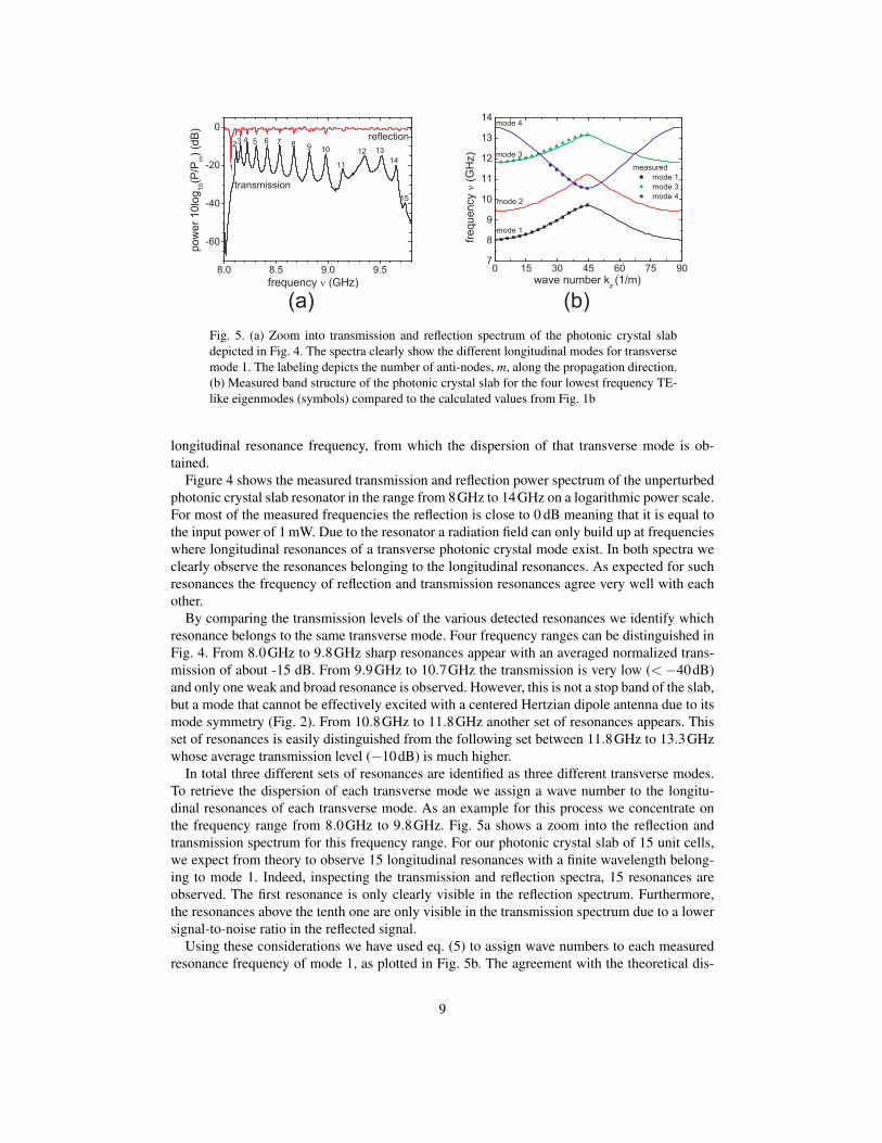
Fig. 5. (a) Zoom into transmission and reflection spectrum of the photonic crystal slabdepicted in Fig. 4. The spectra clearly show the different longitudinal modes for transversemode 1. The labeling depicts the number of anti-nodes, m, along the propagation direction.(b) Measured band structure of the photonic crystal slab for the four lowest frequency TE-like eigenmodes (symbols) compared to the calculated values from Fig. 1b
longitudinal resonance frequency, from which the dispersion of that transverse mode is ob-tained.
Figure 4 shows the measured transmission and reflection power spectrum of the unperturbedphotonic crystal slab resonator in the range from 8GHz to 14GHz on a logarithmic power scale.For most of the measured frequencies the reflection is close to 0 dB meaning that it is equal tothe input power of 1 mW. Due to the resonator a radiation field can only build up at frequencieswhere longitudinal resonances of a transverse photonic crystal mode exist. In both spectra weclearly observe the resonances belonging to the longitudinal resonances. As expected for suchresonances the frequency of reflection and transmission resonances agree very well with eachother.
By comparing the transmission levels of the various detected resonances we identify whichresonance belongs to the same transverse mode. Four frequency ranges can be distinguished inFig. 4. From 8.0GHz to 9.8GHz sharp resonances appear with an averaged normalized trans-mission of about -15 dB. From 9.9GHz to 10.7GHz the transmission is very low (< −40dB)and only one weak and broad resonance is observed. However, this is not a stop band of the slab,but a mode that cannot be effectively excited with a centered Hertzian dipole antenna due to itsmode symmetry (Fig. 2). From 10.8GHz to 11.8GHz another set of resonances appears. Thisset of resonances is easily distinguished from the following set between 11.8GHz to 13.3GHzwhose average transmission level (−10dB) is much higher.
In total three different sets of resonances are identified as three different transverse modes.To retrieve the dispersion of each transverse mode we assign a wave number to the longitu-dinal resonances of each transverse mode. As an example for this process we concentrate onthe frequency range from 8.0GHz to 9.8GHz. Fig. 5a shows a zoom into the reflection andtransmission spectrum for this frequency range. For our photonic crystal slab of 15 unit cells,we expect from theory to observe 15 longitudinal resonances with a finite wavelength belong-ing to mode 1. Indeed, inspecting the transmission and reflection spectra, 15 resonances areobserved. The first resonance is only clearly visible in the reflection spectrum. Furthermore,the resonances above the tenth one are only visible in the transmission spectrum due to a lowersignal-to-noise ratio in the reflected signal.
Using these considerations we have used eq. (5) to assign wave numbers to each measuredresonance frequency of mode 1, as plotted in Fig. 5b. The agreement with the theoretical dis-
9

(a)
(b)
Fig. 6. (a) Measured frequency shift ∆ν induced by placing the spherical scatterer at thatlocation. Shown is the frequency shift ∆ν for mode 1 at a longitudinal resonance with ν =8.16GHz and kzaz,eff =
115 π . (b) Resulting electric field component Ez from the measured
frequency shift shown in (a) versus position. The measured electric field component Ez(symbols) is compared to the calculated electric field (lines).
persion (solid lines) is excellent. To assign also wave numbers to higher order modes we takeinto account, as was explained above, that mode 2 is not effectively excited with the centeredHertzian dipole antenna. Furthermore, the resonances of mode 4 can only be partly observed.Mode 4 overlaps in frequency with mode 3, but mode 3 couples better to the antenna as can beseen from the higher transmission level of mode 3. Hence, only mode 3 is detected where bothmodes overlap.
With these considerations we can assign normalized wave numbers to mode 3 and mode4, as well. Also for these modes the agreement with the theoretical dispersion (solid lines) isexcellent. In conclusion, the excellent agreement for mode 1 to mode 4 indicates an appropriatedescription of the fabricated slab with FDTD calculations.
6. Electric field measurements
We measure the longitudinal electric field inside the photonic crystal slab by measuring thefrequency shift of an individual longitudinal resonance due to a spherical metal scatterer insidethe crystal. By scanning the position of the scatterer we can map the electric field distribution.Note that the measured frequency shift ∆ν is referenced to the resonance frequency of theresonator loaded by the nylon string alone. The effect of the nylon string is small as it results ina shift of only 250kHz.
Figure 6a and 7a show two examples of the measured frequency shift ∆ν for mode 1 due tothe scatterer. The frequencies of the two longitudinal resonances are 8.16GHz and 8.42GHz,respectively. The uncertainty of the frequency shift is 250kHz due to the frequency resolutionof the network analyzer. In both measurements the frequency shift remains always smaller orequal to zero, as we expect from eq.(2) for a mode with a dominating Ez field component.Towards the edge of the waveguide the frequency shift ∆ν approaches zero. As can be seenfrom Fig. 2, the electric field Ez is at these location close to zero and consequently also thefrequency shift. The strongest frequency shift of about 4.75MHz and 2.25MHz, respectively,is reached in both examples at about 7.0mm from the center. In between two rows of rods the
10

(a)
(b)
Fig. 7. (a) Measured frequency shift ∆ν induced by placing the spherical scatterer at thatlocation. Shown is the frequency shift ∆ν for mode 1 at a longitudinal resonance with ν =8.42GHz and kzaz,eff =
615 π (b) Resulting electric field component Ez from the measured
frequency shift shown in (a) versus position. The measured electric field component Ez(symbols) is compared to the calculated electric field (lines).
strongest Ez field component along the x-direction is generally not located at the center of thewaveguide but located slightly off the center, see Fig. 2.
To calculate the longitudinal electric field Ez from the measured frequency shift we apply eq.(3). However, this requires to determine the total energy stored inside the cavity U . To retrieveU we use the definition of the quality factor:
Q = 2πν0U
Pdiss. (6)
Exactly at resonance the dissipated power per cycle Pdiss is equal to the input power Pin fromthe network analyzer. To retrieve the experimental Q-values we determine the full width halfmaximum of each transmission resonance νFWHM shown in Fig. 5a and use Q = ν0/νFWHM .
Figure 6b and 7b shows the resulting electric field strength Ez (square dots) determined forthe two longitudinal resonances of mode 1 at a frequency of 8.16GHz and 8.42GHz, respec-tively. For a comparison, the figure displays also the Ez field strength from the FDTD cal-culations presented in section 2 (black line). Uncertainties for the measured field values aredetermined by using the Gaussian error propagation law. We assume that the dominating errorsare the uncertainty in input power of about 10 % and the frequency resolution of 250 kHz. Allother uncertainties are much smaller and do not significantly contribute to the error bars of themeasurement.
Figure 6 shows the results for a longitudinal resonance with a frequency of 8.16GHz. Theoverall shape of the electric field shows an excellent agreement to the calculated field strength.Furthermore, also the absolute values agree within the range of the measurement accuracy,although no adjustable parameter is used in the calculations. Figure 7 shows an example at ahigher frequency of 8.42GHz. The agreement between FDTD calculations and experiment isagain very good. This holds both for the shape of the profile and also for the absolute values.Minor deviations are visible at the waveguide center. The small difference between electricfield maximum and central electric field value at the center is calculated to be about 7 V/mm
11

which is not resolved in the measurements. In addition, the measured absolute field value isslightly lower. We tentatively attribute both effects to the fact that at a higher frequency (shorterwavelength) influences due to non-periodic variations in the photonic crystal become moreimportant. Nevertheless, in both examples a good agreement between experiment and theory isfound.
The two discussed examples for mapping the electric field component Ez illustrate the ca-pability of the method to map the absolute value of a specific electric field component insidea photonic crystal. The good agreement between the measurements and calculations furtherclearly demonstrates that a field mapping inside a photonic crystal is possible.
7. Summary and outlook
We have demonstrated for the first time a method for mapping the absolute strength of an elec-tromagnetic field component inside a photonic crystal. The method relies on measuring thechange in resonance frequency when the photonic crystal is placed inside a resonator and thefield inside the photonic crystal is perturbed by a sub-wavelength scatterer. A spherical scattereris applied to measure the dominating longitudinal electric field Ez in a specific photonic crystalslab. We observe a good agreement between measured and calculated electric field strength Ezwithout using any adjustable parameters in the calculations. Note that even if all six compo-nents would be of comparable strength, such as in an arbitrary photonic crystal or at specificlocations, it is still possible to separately measure each field component. This can be achievedby selecting for the scatterer a suitable material, shape and orientation such that only a singlefield component contributes to the frequency shift [43, 44]. For example, a thin metallic needlewould short-circuit and thus probe the electric field along the orientation of the needle whileleaving all other field components unaffected.
In the future, this method could be applied in the near infrared or optical domain by scalingdown the photonic crystal and the bead on a string. To induce a space dependent frequency shifta metallic or dielectric scatterer could be placed on a carbon nanotube acting as a string. Tocontrol the nanotube it could be attached to an atomic force microscope tip. Mounting a carbonnanotube on an atomic force microscope has been demonstrated [51]. Further, atomic forcemicroscopy allows a sufficiently high spatial resolution, demonstrated by recent measurementswhere an emitter directly mounted to an atomic force microscope has been used to map theemitter lifetime around a single nanorod [52]. Combining these results it should be possible tomeasure the shift in resonance frequency in the transmission spectrum to determine the absolutefield strength inside the air voids of a photonic crystal at optical frequencies.
8. Acknowledgment
This research is supported by the Dutch Technology Foundation STW, applied science divisionof NWO and the Technology Program of the Ministry of Economic Affairs. The authors furtherthank ESA-ESTEC for providing part of the RF-equipment. The research is also part of thestrategic research orientation Applied Nanophotonics within the MESA+ Research Institute.
12