Transfer of photonic crystal membranes to a transparent gel substrate
10
Transfer of photonic crystal membranes to a transparent gel substrate Lj. Babi´ c, 1 R. Leijssen, 1 E.F.C. Driessen, 1,2 and M.J.A. de Dood 1, ∗ 1 Huygens Laboratory, Leiden University, Niels Bohrweg 2, 2333 CA Leiden, The Netherlands 2 Kavli Institute of Nanoscience, Delft University of Technology, Lorentzweg 1, 2628 CJ Delft, The Netherlands ∗ [email protected] Abstract: We report a method of transferring 150 nm thick Al 0.35 Ga 0.65 As photonic crystal slabs to a transparent gel, without compromising their optical properties. We demonstrate successful transfer for membranes as large as ∼ 425 × 425 μ m 2 . The transfer results in a 2.5% frequency red shift and increases the visibility of the resonances in reflection spectra. The avoided crossings between the modes show a subradiant mode with quality factors up to ∼300. This suggests that the quality factor is only limited by the finite size of the crystal. © 2011 Optical Society of America OCIS codes: (220.4000) Microstructure fabrication; (050.5298) Photonic crystals; (260.5740) Resonance; (050.1940) Diffraction. References and links 1. M. Notomi, “Manipulating light with strongly modulated photonic crystals,” Rep. Prog. Phys. 73, 096501 (2010). 2. T. Yoshie, A. Scherer, J. Hendrickson, G. Khitrova, H. M. Gibbs, G. Rupper, C. Ell, O. B. Shchekin, and D. G. Deppe, “Vacuum Rabi splitting with a single quantum dot in a photonic crystal nanocavity,” Nature 432, 9–12 (2004). 3. K. Hennessy, A. Badolato, M. Winger, D. Gerace, M. Atat¨ ure, S. Gulde, S. F¨ alt, E. L. Hu, and A. Imamoglu, “Quantum nature of a strongly coupled single quantum dot-cavity system.” Nature 445, 896–899 (2007). 4. J. J. Wierer, A. David, and M. M. Megens, “III-nitride photonic-crystal light-emitting diodes with high extraction efficiency with high extraction efficiency,” Nat. Photonics 3, 163–169 (2009). 5. J. P. Mondia, H. M. van Driel, W. Jiang, A. R. Cowan, and J. F. Young, “Enhanced second-harmonic generation from planar photonic crystals,” Opt. Lett. 28, 2500–2502 (2003). 6. Y. Dumeige, I. Sagnes, P. Monnier, P. Vidakovic, I. Abram, C. M´ eriadec, and A. Levenson, “Phase-matched frequency doubling at photonic band edges: efficiency scaling as the fifth power of the length,” Phys. Rev. Lett. 89, 043901 (2002). 7. A. D. Bristow, J. P. Mondia, and H. M. van Driel, “Sum and difference frequency generation as diagnostics for leaky eigenmodes in two-dimensional photonic crystal waveguides,” J. Appl. Phys. 99, 023105 (2006). 8. P. Kopperschmidt, S. Senz, G. K¨ astner, D. Hesse, and U. M. G¨ osele, “Materials integration of gallium arsenide and silicon by wafer bonding,” Appl. Phys. Lett. 72, 3181–3183 (1998). 9. Z. Hatzopoulos, D. Cenghera, G. Deligeorgisa, M. Androulidakia, E. Aperathitisa, and G. H. A. Georgakilas, “Molecular beam epitaxy of GaAs/AlGaAs epitaxial structures for integrated optoelectronic devices on Si using GaAs-Si wafer bonding,” J. Cryst. Growth 227–228, 193–196 (2001). 10. P. Kopperschmidt, G. K¨ astner, S. Senz, D. Hesse, and U. G¨ osele, “Wafer bonding of gallium arsenide on sap- phire,” Appl. Phys. A 64, 533–537 (1997). 11. E. Chow, A. Grot, L. W. Mirkarimi, M. Sigalas, and G. Girolami, “Ultracompact biochemical sensor built with two-dimensional photoniccrystal microcavity,” Opt. Lett. 29, 1093–1095 (2004). 12. T. van der Sar, E. C. Heeres, G. M. Dmochowski, G. de Lange, L. Robledo, T. H. Oosterkamp, and R. Hanson, “Nanopositioning of a diamond nanocrystal containing a single nitrogen-vacancy defect center,” Appl. Phys. Lett. 94, 173104 (2009). 13. D. Englund, B. Shields, K. Rivoire, F. Hatami, J. Vuˇ ckoviˇ c, H. Park, and M. D. Lukin, “Deterministic coupling of a single nitrogen vacancy center to a photonic crystal cavity,” Nano Lett. 10, 3922–3926 (2010). #151322 - $15.00 USD Received 19 Jul 2011; revised 16 Aug 2011; accepted 29 Aug 2011; published 22 Sep 2011 (C) 2011 OSA 26 September 2011 / Vol. 19, No. 20 / OPTICS EXPRESS 19532
-
Upload
leidenuniv -
Category
Documents
-
view
1 -
download
0
Transcript of Transfer of photonic crystal membranes to a transparent gel substrate
Transfer of photonic crystal membranesto a transparent gel substrate
Lj. Babi c,1 R. Leijssen,1 E.F.C. Driessen,1,2 and M.J.A. de Dood1,∗
1 Huygens Laboratory, Leiden University, Niels Bohrweg 2, 2333 CA Leiden, The Netherlands2 Kavli Institute of Nanoscience, Delft University of Technology, Lorentzweg 1, 2628 CJ Delft,
The Netherlands∗[email protected]
Abstract: We report a method of transferring 150 nm thick Al0.35Ga0.65Asphotonic crystal slabs to a transparent gel, without compromising theiroptical properties. We demonstrate successful transfer for membranes aslarge as∼ 425×425µm2. The transfer results in a 2.5% frequency redshift and increases the visibility of the resonances in reflection spectra. Theavoided crossings between the modes show a subradiant mode with qualityfactors up to∼300. This suggests that the quality factor is only limited bythe finite size of the crystal.
© 2011 Optical Society of America
OCIS codes:(220.4000) Microstructure fabrication; (050.5298) Photonic crystals; (260.5740)Resonance; (050.1940) Diffraction.
References and links1. M. Notomi, “Manipulating light with strongly modulated photonic crystals,” Rep. Prog. Phys.73, 096501 (2010).2. T. Yoshie, A. Scherer, J. Hendrickson, G. Khitrova, H. M. Gibbs, G. Rupper, C. Ell, O. B. Shchekin, and D. G.
Deppe, “Vacuum Rabi splitting with a single quantum dot in a photonic crystal nanocavity,” Nature432, 9–12(2004).
3. K. Hennessy, A. Badolato, M. Winger, D. Gerace, M. Atature, S. Gulde, S. Falt, E. L. Hu, and A. Imamoglu,“Quantum nature of a strongly coupled single quantum dot-cavity system.” Nature445, 896–899 (2007).
4. J. J. Wierer, A. David, and M. M. Megens, “III-nitride photonic-crystal light-emitting diodes with high extractionefficiency with high extraction efficiency,” Nat. Photonics3, 163–169 (2009).
5. J. P. Mondia, H. M. van Driel, W. Jiang, A. R. Cowan, and J. F. Young, “Enhanced second-harmonic generationfrom planar photonic crystals,” Opt. Lett.28, 2500–2502 (2003).
6. Y. Dumeige, I. Sagnes, P. Monnier, P. Vidakovic, I. Abram, C. Meriadec, and A. Levenson, “Phase-matchedfrequency doubling at photonic band edges: efficiency scaling as the fifth power of the length,” Phys. Rev. Lett.89, 043901 (2002).
7. A. D. Bristow, J. P. Mondia, and H. M. van Driel, “Sum and difference frequency generation as diagnostics forleaky eigenmodes in two-dimensional photonic crystal waveguides,” J. Appl. Phys.99, 023105 (2006).
8. P. Kopperschmidt, S. Senz, G. Kastner, D. Hesse, and U. M. Gosele, “Materials integration of gallium arsenideand silicon by wafer bonding,” Appl. Phys. Lett.72, 3181–3183 (1998).
9. Z. Hatzopoulos, D. Cenghera, G. Deligeorgisa, M. Androulidakia, E. Aperathitisa, and G. H. A. Georgakilas,“Molecular beam epitaxy of GaAs/AlGaAs epitaxial structures for integrated optoelectronic devices on Si usingGaAs-Si wafer bonding,” J. Cryst. Growth227–228, 193–196 (2001).
10. P. Kopperschmidt, G. Kastner, S. Senz, D. Hesse, and U. Gosele, “Wafer bonding of gallium arsenide on sap-phire,” Appl. Phys. A64, 533–537 (1997).
11. E. Chow, A. Grot, L. W. Mirkarimi, M. Sigalas, and G. Girolami, “Ultracompact biochemical sensor built withtwo-dimensional photoniccrystal microcavity,” Opt. Lett.29, 1093–1095 (2004).
12. T. van der Sar, E. C. Heeres, G. M. Dmochowski, G. de Lange, L. Robledo, T. H. Oosterkamp, and R. Hanson,“Nanopositioning of a diamond nanocrystal containing a single nitrogen-vacancy defect center,” Appl. Phys.Lett. 94, 173104 (2009).
13. D. Englund, B. Shields, K. Rivoire, F. Hatami, J. Vuckovic, H. Park, and M. D. Lukin, “Deterministic couplingof a single nitrogen vacancy center to a photonic crystal cavity,” Nano Lett.10, 3922–3926 (2010).
#151322 - $15.00 USD Received 19 Jul 2011; revised 16 Aug 2011; accepted 29 Aug 2011; published 22 Sep 2011(C) 2011 OSA 26 September 2011 / Vol. 19, No. 20 / OPTICS EXPRESS 19532
14. K. M. Ho, C. T. Chan, and C. M. Soukoulis, “Existence of a photonic gap in periodic dielectric structures,” Phys.Rev. Lett.65, 3152–3155 (1990).
15. R. D. Meade, K. D. Brommer, A. M. Rappe, and J. D. Joannopoulos, “Existence of a photonic band gap in twodimensions,” Appl. Phys. Lett.61, 495–497 (1992).
16. C. T. Chan, S. Datta, K. M. Ho, and C. M. Soukoulis, “A7 structure: a family of photonic crystals,” Phys. Rev. B50, 1988–1991 (1994).
17. T. Maeda, J. Lee, R. Shul, J. Han, J. Hong, E. Lambers, S. Pearton, C. Abernathy, and W. Hobson, “Induc-tively coupled plasma etching of III-V semiconductors in BCl3-based chemistries. I. GaAs, GaN, GaP, GaSb andAlGaAs,” Appl. Surf. Sci.143, 174–182 (1999).
18. E. F. C. Driessen, D. Stolwijk, and M. J. A. de Dood, “Asymmetry reversal in the reflection from a two-dimensional photonic crystal,” Opt. Lett.32, 3137–3139 (2007).
19. L. Babic and M. J. A. de Dood, “Interpretation of the fano lineshape reversal in the reflectivity spectra of photoniccrystal slabs,” Opt. Express18, 26569–26582 (2011).
20. Detailed information and technical datasheets are available via the manufacturers website:http://www.gelpak.com
21. http://www.ioffe.ru/SVA/NSM/Semicond/AlGaAs/index.html.22. The forceFs to peel off the membrane breaking all gel-membrane bonds on the surface is proportional toL×
(1− π(r/a)2)). The force needed to break the membrane freeFb is given by the work needed to peel freethe membranes along the sides and givesFb ∝ d × (a− 2r). The ratio between the two forcesFs/Fb is then
proportional toLd × 1−π(r/a)2
a−2r , where the second term is a geometrical factor that accounts for the square latticeof air holes in the membrane.
23. M. Kanskar, P. Paddon, V. Pacradouni, R. Morin, A. Busch, J. F. Young, S. R. Johnson, J. MacKenzie, andT. Tiedje, “Observation of leaky slab modes in an air-bridged semiconductor waveguide with a two-dimensionalphotonic lattice,” Appl. Phys. Lett.70, 1438–1440 (1997).
24. V. N. Astratov, D. M. Whittaker, I. S. Culshaw, R. M. Stevenson, M. S. Skolnick, T. F. Krauss, and R. M. De LaRue, “Photonic band-structure effects in the reflectivity of periodically patterned waveguides,” Phys. Rev. B60,R16255–R16258 (1999).
25. S. Fan, W. Suh, and J. D. Joannopoulos, “Temporal coupled-mode theory for the fano resonance in opticalresonators,” J. Opt. Soc. Am. A20, 569–572 (2003).
26. T. Ochiai and K. Sakoda, “Nearly free-photon approximation for two-dimensional photonic crystal slabs,” Phys.Rev. B64, 045108 (2001).
27. K. B. Crozier, V. Lousse, O. Kilic, S. Kim, S. Fan, and O. Solgaard, “Air-bridged photonic crystal slabs at visibleand near-infrared wavelengths,” Phys. Rev. B73, 115126 (2006).
28. W. L. Barnes, T. W. Preist, S. C. Kitson, and J. R. Sambles, “Physical origin of photonic energy gaps in thepropagation of surface plasmons on gratings,” Phys. Rev. B54, 6227–6244 (1996).
29. C. Ropers, D. J. Park, G. Stibenz, G. Steinmeyer, J. Kim, D. S. Kim, and C. Lienau, “Femtosecond light trans-mission and subradiant damping in plasmonic crystals,” Phys. Rev. Lett.94, 113901 (2005).
30. M. J. A. de Dood, E. F. C. Driessen, D. Stolwijk, and M. P. van Exter, “Observation of coupling between surfaceplasmons in index-matched hole arrays,” Phys. Rev. B77, 115437 (2008).
31. J. Wiersig, “Formation of long-lived, scarlike modes near avoided resonance crossings in optical microcavities,”Phys. Rev. Lett.97, 253901 (2006).
32. Q. H. Song and H. Cao, “Improving optical confinement in nanostructures via external mode coupling,” Phys.Rev. Lett.105, 053902 (2010).
33. P. Paddon and J. Young, “Two-dimensional vector-coupled-mode theory for textured planar waveguides,” Phys.Rev. B61, 2090–2101 (2000).
34. A. R. Cowan and Jeff F. Young, “Mode matching for second-harmonic generation in photonic crystal waveg-uides,” Phys. Rev. B65, 085106 (2002).
35. J. Torres, D. Coquillat, R. Legros, J. P. Lascaray, F. Teppe, D. Scalbert, D. Peyrade, Y. Chen, O. Briot, M. LeVassor d’Yerville, E. Centeno, D. Cassagne, and J. P. Albert, “Giant second-harmonic generation in a one-dimensional gan photonic crystal,” Phys. Rev. B69, 085105 (2004).
36. F. Jelezko, A. Volkmer, I. Popa, K. K. Rebane, and J. Wrachtrup, “Coherence length of photons from a singlequantum system,” Phys. Rev. A67, 041802 (2003).
1. Introduction
Photoniccrystals, in particular photonic crystal cavities, have been very succesful in creatingstrong interactions between light and matter [1]. The strong confinement provided by the largerefractive index difference between GaAs and air in a two-dimensional photonic crystal slabenables a single quantum dot emitter to reach the strong-coupling regime [2, 3]. Many otherapplications, such as small mode volume lasers, light-emitting diodes [4], nonlinear interac-
#151322 - $15.00 USD Received 19 Jul 2011; revised 16 Aug 2011; accepted 29 Aug 2011; published 22 Sep 2011(C) 2011 OSA 26 September 2011 / Vol. 19, No. 20 / OPTICS EXPRESS 19533
tions [5–7], and nanoscale sensors all benefit from the strong confinement of light, and use in-trinsic emission of III-V semiconductors as an internal light source. Although well establishedfabrication protocols exist to create nanophotonic devices in layers of III-V semiconductorsgrown on an epitaxial support wafer, it is not obvious how to transfer these devices to othersubstrate materials. Wafer bonding techniques exist to transfer (Al)GaAs layers to silicon [8,9]or optically transparent sapphire [10] substrates. These wafer bonding methods are done athigh temperatures with flat, unpatterned substrates and cannot be applied to transfer an exist-ing nanostructure. Therefore, an alternative method that allows to transfer existing devices toother substrates at room temperature are highly desirable. Such a method would greatly facil-itate the use of photonic crystal devices in a wide range of applications and environments, forinstance in biochemical sensors in liquid phase [11] or to couple single nitrogen-vacany centersin diamond [12,13] to a cavity for quantum information purposes.
In this letter we show that it is possible to transfer a 150 nm thick Al0.35Ga0.65As photoniccrystal membranes with a square lattice of holes, to a gel substrate that can be combined withany other material of choice. The gel substrate is optically transparent and has a relatively lowrefractive index which allows for a large refractive index contrast with the Al0.35Ga0.65As ma-terial of the photonic crystal. This large contrast is necessary in order to create structures witha band gap of guided modes that can support photonic crystal cavities [14–16]. We study thetransferred structures in detail using reflection and transmission measurements, and comparethese results to similar measurements on the same membrane before transfer. From this com-parison, we infer that the optical properties of a photonic crystal membrane on gel are similar oreven improved compared to the optical properties of the freestanding structure before transfer.
2. Sample fabrication and transfer to a gel
The square lattice photonic crystal structures in this study are fabricated in a 150 nm thickAl0.35Ga0.65As layer on top of a 1µm thick Al0.7Ga0.3As sacrificial layer. Regular arrays ofholes are defined using standard e-beam lithography and reactive ion etching techniques in achlorine based plasma [17]. Freestanding membranes with an area up to∼ 425×425µm2 arecreated by removal of the sacrificial layer in hydrofluoric acid followed by critical point drying.Details of the fabrication process are published elsewhere [18,19].
Figure 1 shows a schematic of the transfer process (a) and optical microscope images be-fore (b) and after (c) the transfer process. The transfer of the membranes is accomplishedby attaching a commercial gel layer of highly cross-linked polymer (gel-pak gel-film PF, re-tention level X4, 0.15 mm thickness [20]) to a glass microscope slide. The sample is thencarefully pushed into the gel layer and the substrate is gently peeled off in the last step. Thesmall lattice mismatch between the Al0.35Ga0.65As (l = 0.565603 nm) top layer and the GaAs(l = 0.565325 nm) substrate [21] together with a thin oxide film on the membrane generatescompressive strain in the membrane and causes the membrane to buckle. The buckling of themembrane before the transfer is best illustrated by the atomic force microscopy (AFM) image(d), since this gives absolute height information. Based on AFM and optical microcopy imagesmade with a double beam interference objective (Nikon, M plan 20 DI), we find height varia-tions up to 10µm before the transfer. Images with the interference objective show that heightvariations are reduced to well below 1µm after the transfer process.
We have tested the transfer technique for 150 nm thick membranes with different membranesizes (∼10× 10 µm2 up to ∼ 425× 425µm2), photonic crystal lattice constants (350 nm≤ a ≤ 960 nm), and hole radii (100 nm≤ r ≤ 270 nm). The transfer process is successfulfor membranes larger than∼ 30× 30 µm2. The important parameter for the transfer is theratio between the force that connects the membrane to the gel and the force needed to breakthe membrane free from the substrate. In both cases the minimum force needed is given by
#151322 - $15.00 USD Received 19 Jul 2011; revised 16 Aug 2011; accepted 29 Aug 2011; published 22 Sep 2011(C) 2011 OSA 26 September 2011 / Vol. 19, No. 20 / OPTICS EXPRESS 19534

a)
50 μm 50 μm 2.5 μm
500 nm
0 nm
c) d)b)
Fig. 1. Transfer of a photonic crystal membrane to a gel. (a) Schematic drawing of theprocess. (b) Optical microscope images of 300×300µm2 large photonic crystal membranebefore (b) and after (c) the transfer. The membrane is 150 nm thick, and contains a squarelattice of 300 nm diameter holes with a lattice constanta = 820 nm. (d) Atomic forcemicroscope image of a 12× 12 µm2 section of a similar membrane (300 nm diameterholes,a = 640 nm) before the transfer, showing typical height variations.
a peeling process where bonds are broken line-by-line instead of all the bonds at once. Thetotal energy required to break all gel-to-membrane bonds scales with the areaL2, while theenergy required to break all atomic bonds along the edges of the membranes scales withL×d,with L andd the membrane dimensions and thickness respectively. Since the forces both actover a distanceL the ratio of the two forces is proportional toLd [22]. Out of a total of∼50transferred membranes, only the first 5 membranes sustained significant damage in the transferprocess. We estimate that a device yield> 90% is possible. Membranes that break or stick tothe substrate either during or after the wet-chemical underetching step in the fabrication canstill be successfully transferred to the gel. This opens a route to creating large photonic crystalmembranes without the use of critical point drying.
3. Optical properties
To test the quality of the optical structures, both before and after the transfer, we performreflection and transmission measurements for wavelengths between 650 and 1700 nm usinga fiber coupled halogen lamp in combination with fiber coupled spectrometers. The spectralresolution varies from 1.5 nm to 3.0 nm over the wavelength range. Apertures placed in thebeam limit the numerical aperture of the incident beam to NA< 0.025. The polarization ofthe incident beam is controlled by a Glan-Thompson polarizing beamsplitter cube. In this way,the reflection and transmission for boths- and p-polarized light are measured as a function ofwavelength and angle of incidence.
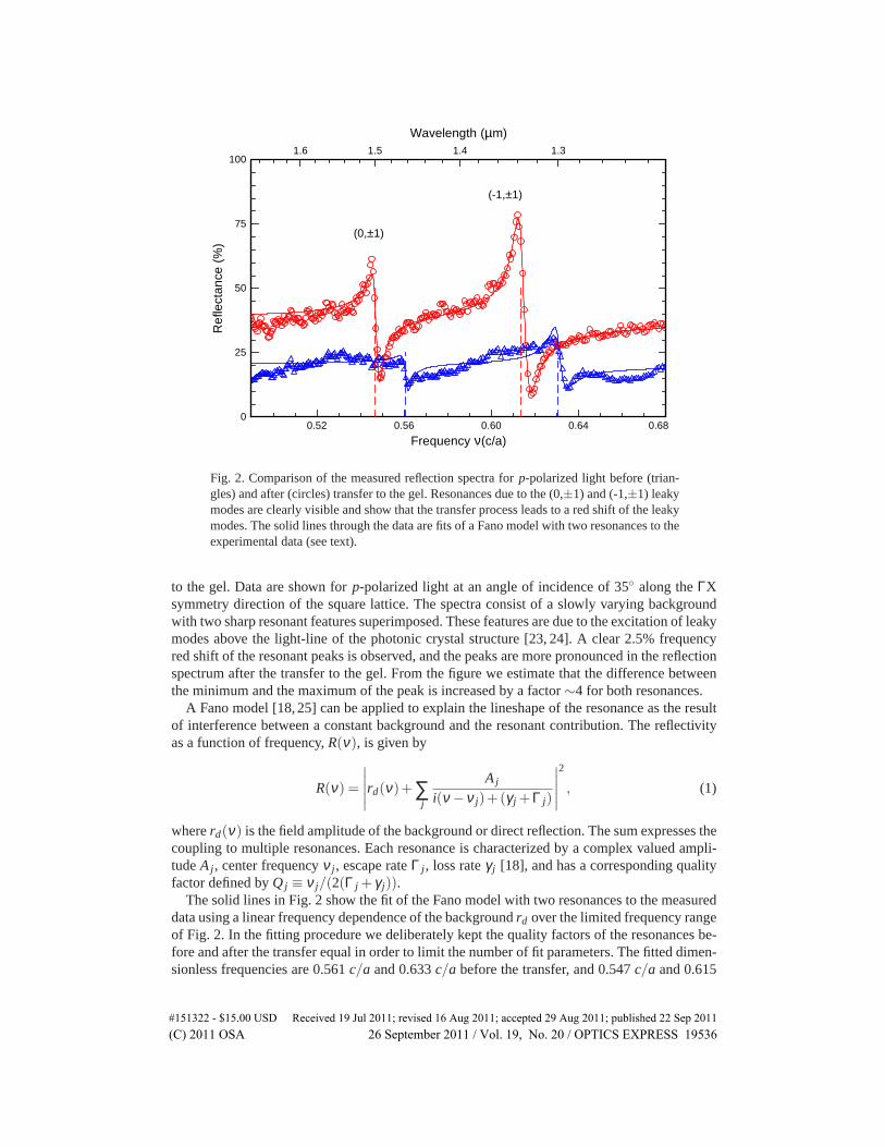
Figure 2 compares the reflectance spectra before (triangles) and after (circles) the transfer
#151322 - $15.00 USD Received 19 Jul 2011; revised 16 Aug 2011; accepted 29 Aug 2011; published 22 Sep 2011(C) 2011 OSA 26 September 2011 / Vol. 19, No. 20 / OPTICS EXPRESS 19535
0.52 0.56 0.60 0.64 0.68
Frequency ν(c/a)
0
25
50
75
100
Ref
lect
ance
(%)
1.31.41.51.6
Wavelength (µm)
(0,±1)
(-1,±1)
Fig. 2. Comparison of the measured reflection spectra forp-polarized light before (trian-gles) and after (circles) transfer to the gel. Resonances due to the (0,±1) and (-1,±1) leakymodes are clearly visible and show that the transfer process leads to a red shift of the leakymodes. The solid lines through the data are fits of a Fano model with two resonances to theexperimental data (see text).
to the gel. Data are shown forp-polarized light at an angle of incidence of 35◦ along theΓXsymmetry direction of the square lattice. The spectra consist of a slowly varying backgroundwith two sharp resonant features superimposed. These features are due to the excitation of leakymodes above the light-line of the photonic crystal structure [23, 24]. A clear 2.5% frequencyred shift of the resonant peaks is observed, and the peaks are more pronounced in the reflectionspectrum after the transfer to the gel. From the figure we estimate that the difference betweenthe minimum and the maximum of the peak is increased by a factor∼4 for both resonances.
A Fano model [18, 25] can be applied to explain the lineshape of the resonance as the resultof interference between a constant background and the resonant contribution. The reflectivityas a function of frequency,R(ν), is given by
R(ν) =
∣
∣
∣
∣
∣
rd(ν)+∑j
A j
i(ν −ν j)+(γ j +Γ j)
∣
∣
∣
∣
∣
2
, (1)
whererd(ν) is the field amplitude of the background or direct reflection. The sum expresses thecoupling to multiple resonances. Each resonance is characterized by a complex valued ampli-tudeA j, center frequencyν j, escape rateΓ j, loss rateγ j [18], and has a corresponding qualityfactor defined byQ j ≡ ν j/(2(Γ j + γ j)).
The solid lines in Fig. 2 show the fit of the Fano model with two resonances to the measureddata using a linear frequency dependence of the backgroundrd over the limited frequency rangeof Fig. 2. In the fitting procedure we deliberately kept the quality factors of the resonances be-fore and after the transfer equal in order to limit the number of fit parameters. The fitted dimen-sionless frequencies are 0.561c/a and 0.633c/a before the transfer, and 0.547c/a and 0.615
#151322 - $15.00 USD Received 19 Jul 2011; revised 16 Aug 2011; accepted 29 Aug 2011; published 22 Sep 2011(C) 2011 OSA 26 September 2011 / Vol. 19, No. 20 / OPTICS EXPRESS 19536

c/a after the transfer, corresponding to red shifts of 2.5% and 2.8% respectively. Additionalmeasurements at six different angles (not shown) reveal that the entire measured dispersionrelation is red shifted by∼2.5% in frequency. This is explained by the increase in the effectiverefractive index of the slab by∼2.5% due to the introduction of the gel substrate [26,27].
The increased visibility of the resonances in Fig. 2 after the transfer corresponds to largeramplitudes|A1,2|. From the fit we find that both of these amplitudes are increased by a factor of3. For a lossless, symmetric, case the amplitude|A| of the resonance of the photonic crystal isequal toΓ and is independent of the value ofrd [25]. We explain the increase in the amplitudeby an incoherent contribution tord(ν) in Fig. 1, which directly affects the amplitude|A|. Due tothe buckling of the freestanding membrane variations in the incident angle and in the distancebetween the substrate and the membrane are introduced. Angle variations lead to variations inthe exact resonance frequency and consequently to a lower quality factor, which is not observedin the experimental data. Variations in distance between the membrane and the substrate thatare much larger thanλ/4 leads to variations in the phase and amplitude ofrd(ν) over theillumination spot which lowers the visibility of the Fano interference.
4. Quality factors and dispersion relation of the resonances.
Figure 3 shows a grayscale plot of the measured transmission fors-polarized light as a functionof frequency (vertical axis) and wavevectork‖ (horizontal axis). The wavevector is varied alongtheΓX andΓM symmetry directions of the square lattice. The figure shows many highly visibledark lines related to the minima of the Fano lineshape of the resonances. Similar resonancesare observed in the transmission data forp-polarized light (not shown, see supporting informa-tion). Higher order resonances are clearly visible in transmission for wavelengths longer than650 nm, demonstrating the high quality of our structure and the potential of the technique forapplications at visible and near infrared wavelengths.
The resonances and their dispersion are due to a coupling of the incoming light to a mode ofthe photonic crystal slab via diffraction from the periodic lattice and are well understood [24,25]. Each of these modes can be labeled by the reciprocal lattice vector(Gx,Gy) responsiblefor the coupling that transforms a waveguide mode of the slab to a guided resonance or leakymode. The corresponding dispersion relation of these leaky modes can be approximated byfolding the calculated dispersion relation of a slab waveguide to the first Brillouin zone of theperiodic structure [26].
A large number of avoided crossings are visible in Fig. 3. Typically, the lower frequencymode in the avoided crossing becomes subradiant and disappears from the transmission spectra,while the higher frequency mode becomes a shorter living superradiant mode [28–30]. This isa result of the coupling between the modes via external radiation [31, 32]. In this case theradiation of the subradiant mode into the surrounding is suppressed by destructive interferenceand the quality factor is considerably enhanced, while the radiation of the superradiant modeis increased via constructive interference. The destructive interference effect on the subradiantmode can be used to gain insight into what limits the linewidth of these resonances after thetransfer to the gel, since it is decoupled from radiative losses to the environment.
In order to investigate what limits the linewidth, we will analyze the avoided crossing of the(1,0) and (-1,±1) modes at an in-plane wavevectork‖ = 0.25×2π/a along theΓX symmetry di-rection at frequencies around 0.6c/a (wavelength of 1.3µm) in detail. This particular crossingis one of the simplest avoided crossings in the system as it involves only three modes related tothe fundamental TE mode of the slab waveguide; two of the three coupled modes are excitedby s-polarized external light, while the third coupled mode is excited byp-polarized externalradiation [26,33].
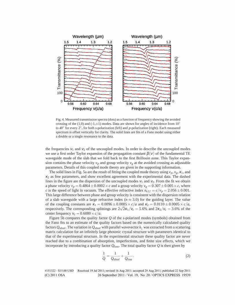
Figure 4 contains the relevant transmission spectra for angles of incidence between 10◦ and
#151322 - $15.00 USD Received 19 Jul 2011; revised 16 Aug 2011; accepted 29 Aug 2011; published 22 Sep 2011(C) 2011 OSA 26 September 2011 / Vol. 19, No. 20 / OPTICS EXPRESS 19537
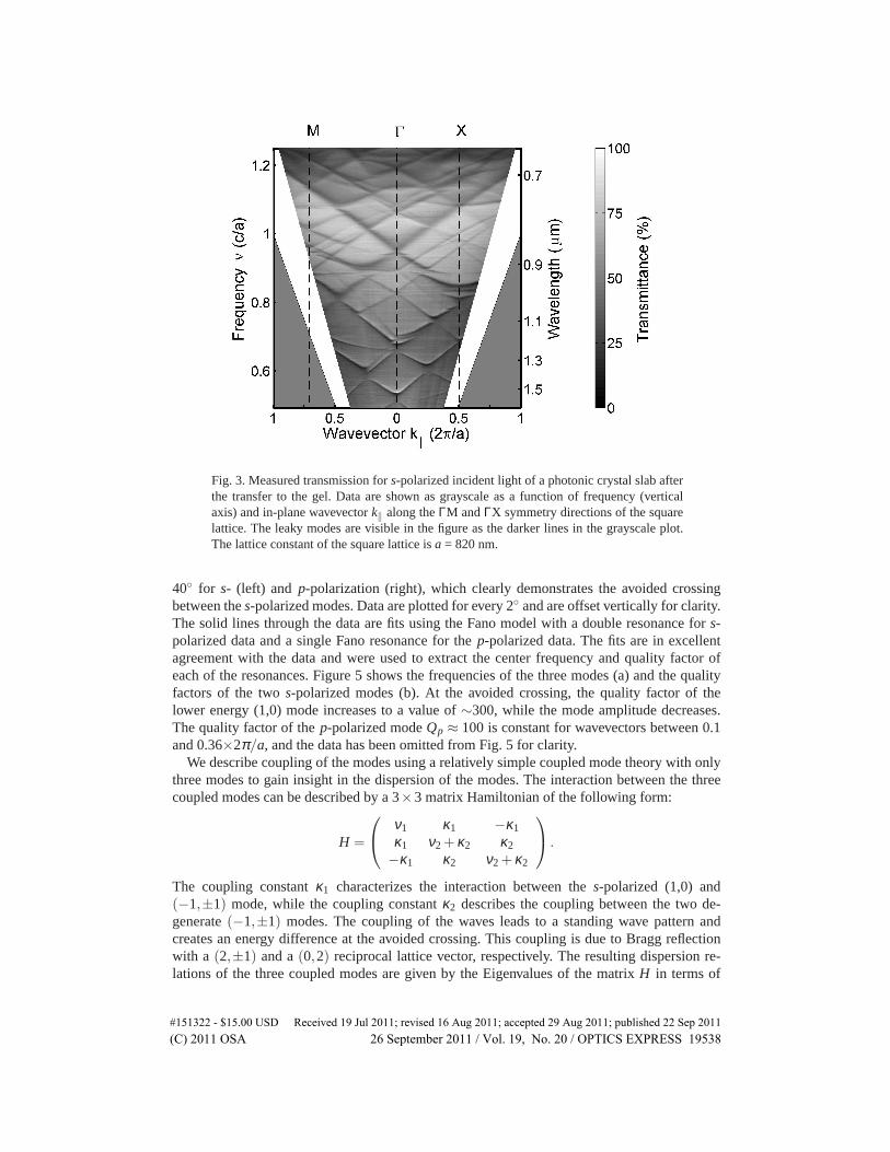
Fig. 3. Measured transmission fors-polarized incident light of a photonic crystal slab afterthe transfer to the gel. Data are shown as grayscale as a function of frequency (verticalaxis) and in-plane wavevectork‖ along theΓM andΓX symmetry directions of the squarelattice. The leaky modes are visible in the figure as the darker lines in the grayscale plot.The lattice constant of the square lattice isa = 820 nm.
40◦ for s- (left) and p-polarization (right), which clearly demonstrates the avoided crossingbetween thes-polarized modes. Data are plotted for every 2◦ and are offset vertically for clarity.The solid lines through the data are fits using the Fano model with a double resonance fors-polarized data and a single Fano resonance for thep-polarized data. The fits are in excellentagreement with the data and were used to extract the center frequency and quality factor ofeach of the resonances. Figure 5 shows the frequencies of the three modes (a) and the qualityfactors of the twos-polarized modes (b). At the avoided crossing, the quality factor of thelower energy (1,0) mode increases to a value of∼300, while the mode amplitude decreases.The quality factor of thep-polarized modeQp ≈ 100 is constant for wavevectors between 0.1and 0.36×2π/a, and the data has been omitted from Fig. 5 for clarity.
We describe coupling of the modes using a relatively simple coupled mode theory with onlythree modes to gain insight in the dispersion of the modes. The interaction between the threecoupled modes can be described by a 3×3 matrix Hamiltonian of the following form:
H =
ν1 κ1 −κ1
κ1 ν2 +κ2 κ2
−κ1 κ2 ν2 +κ2
.
The coupling constantκ1 characterizes the interaction between thes-polarized (1,0) and(−1,±1) mode, while the coupling constantκ2 describes the coupling between the two de-generate(−1,±1) modes. The coupling of the waves leads to a standing wave pattern andcreates an energy difference at the avoided crossing. This coupling is due to Bragg reflectionwith a (2,±1) and a(0,2) reciprocal lattice vector, respectively. The resulting dispersion re-lations of the three coupled modes are given by the Eigenvalues of the matrixH in terms of
#151322 - $15.00 USD Received 19 Jul 2011; revised 16 Aug 2011; accepted 29 Aug 2011; published 22 Sep 2011(C) 2011 OSA 26 September 2011 / Vol. 19, No. 20 / OPTICS EXPRESS 19538
0.56 0.60 0.64 0.68
Frequency ν(c/a)
0
100
1.21.31.41.5
Wavelength (µm)
0.56 0.60 0.64 0.68
Frequency ν(c/a)
Tra
nsm
ittan
ce(%
)
1.21.31.41.5
Wavelength (µm)
0.56 0.60 0.64 0.68
Frequency ν(c/a)
1.21.31.41.5
Wavelength (µm)
0
100
0.56 0.60 0.64 0.68
Frequency ν(c/a)
1.21.31.41.5
Wavelength (µm)
Tra
nsm
ittan
ce(%
)
Fig. 4. Measured transmission spectra (dots) as a function of frequency showing the avoidedcrossingof the (1,0) and (-1,±1) modes. Data are shown for angles of incidence from 10◦
to 40◦ for every 2◦, for boths-polarization (left) andp-polarization (right). Each measuredspectrum is offset vertically for clarity. The solid lines are fits of a Fano model using eithera double or a single resonance to the data.
the frequenciesν1 andν2 of the uncoupled modes. In order to describe the uncoupled modeswe use a first order Taylor expansion of the propagation constantβ (ν) of the fundamental TEwaveguide mode of the slab that we fold back to the first Brillouin zone. This Taylor expan-sion contains the phase velocityvp and group velocityvg at the avoided crossing as adjustableparameters. Details of this coupled mode theory are given in the supporting information.
The solid lines in Fig. 5a are the result of fitting the coupled mode theory usingvp, vg, κ1, andκ2 as free parameters, and show excellent agreement with the experimental data. The dashedlines in the figure are the dispersion of the uncoupled modesν1 andν2. From the fit we obtaina phase velocityvp = 0.4864±0.0002× c and a group velocityvg = 0.307±0.005× c, wherec is the speed of light in vacuum. The effective refractive indexne f f = c/vp = 2.056±0.001.This large difference between phase and group velocity is consistent with the dispersion relationof a slab waveguide with a large refractive index (n≈ 3.0) for the guiding layer. The valueof the coupling constants areκ1 = 0.0096± 0.0005× c/a andκ2 = 0.0110± 0.0005× c/a,respectively. The corresponding splittings are 2
√2κ1/νc = 5.6% and 2κ2/νc = 3.6% of the
center frequencyνc = 0.6080× c/a.Figure 5b compares the quality factorQ of the s-polarized modes (symbols) obtained from
the Fano fits to an estimate of the quality factors based on the numerically calculated qualityfactorsQideal . The variation inQideal with parallel wavevectork‖ was extracted from a scatteringmatrix calculation for an infinitely large photonic crystal structure with parameters identical tothat of the experimental structure. In the experimental structure these quality factor are neverreached due to a combination of absorption, imperfections, and finite size effects, which weincorporate by introducing a quality factorQloss. The total quality factorQ is then given by
1Q
=1
Qideal+
1Qloss
. (2)
#151322 - $15.00 USD Received 19 Jul 2011; revised 16 Aug 2011; accepted 29 Aug 2011; published 22 Sep 2011(C) 2011 OSA 26 September 2011 / Vol. 19, No. 20 / OPTICS EXPRESS 19539
0.1 0.2 0.3 0.4
Wavevector (2π/a)
0.57
0.60
0.63
0.66
Fre
quen
cyν(
c/a)
a)
0.1 0.2 0.3 0.4
Wavevector (2π/a)
0
100
200
300
400
Qua
lity
fact
or
b)
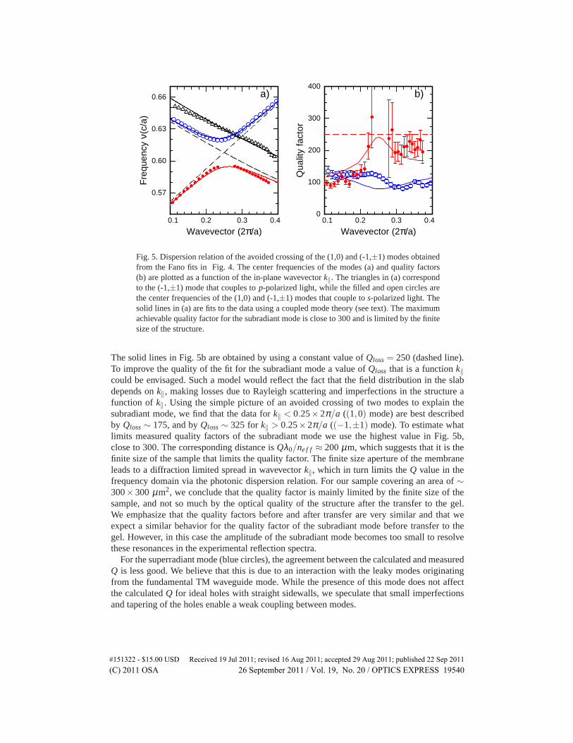
Fig. 5. Dispersion relation of the avoided crossing of the (1,0) and (-1,±1) modes obtainedfrom the Fano fits in Fig. 4. The center frequencies of the modes (a) and quality factors(b) are plotted as a function of the in-plane wavevectork‖. The triangles in (a) correspondto the (-1,±1) mode that couples top-polarized light, while the filled and open circles arethe center frequencies of the (1,0) and (-1,±1) modes that couple tos-polarized light. Thesolid lines in (a) are fits to the data using a coupled mode theory (see text). The maximumachievable quality factor for the subradiant mode is close to 300 and is limited by the finitesize of the structure.
The solid lines in Fig. 5b are obtained by using a constant value ofQloss = 250 (dashed line).To improve the quality of the fit for the subradiant mode a value ofQloss that is a functionk‖could be envisaged. Such a model would reflect the fact that the field distribution in the slabdepends onk‖, making losses due to Rayleigh scattering and imperfections in the structure afunction of k‖. Using the simple picture of an avoided crossing of two modes to explain thesubradiant mode, we find that the data fork‖ < 0.25×2π/a ((1,0) mode) are best describedby Qloss ∼ 175, and byQloss ∼ 325 fork‖ > 0.25×2π/a ((−1,±1) mode). To estimate whatlimits measured quality factors of the subradiant mode we use the highest value in Fig. 5b,close to 300. The corresponding distance isQλ0/ne f f ≈ 200µm, which suggests that it is thefinite size of the sample that limits the quality factor. The finite size aperture of the membraneleads to a diffraction limited spread in wavevectork‖, which in turn limits theQ value in thefrequency domain via the photonic dispersion relation. For our sample covering an area of∼300×300 µm2, we conclude that the quality factor is mainly limited by the finite size of thesample, and not so much by the optical quality of the structure after the transfer to the gel.We emphasize that the quality factors before and after transfer are very similar and that weexpect a similar behavior for the quality factor of the subradiant mode before transfer to thegel. However, in this case the amplitude of the subradiant mode becomes too small to resolvethese resonances in the experimental reflection spectra.
For the superradiant mode (blue circles), the agreement between the calculated and measuredQ is less good. We believe that this is due to an interaction with the leaky modes originatingfrom the fundamental TM waveguide mode. While the presence of this mode does not affectthe calculatedQ for ideal holes with straight sidewalls, we speculate that small imperfectionsand tapering of the holes enable a weak coupling between modes.
#151322 - $15.00 USD Received 19 Jul 2011; revised 16 Aug 2011; accepted 29 Aug 2011; published 22 Sep 2011(C) 2011 OSA 26 September 2011 / Vol. 19, No. 20 / OPTICS EXPRESS 19540
5. Conclusion
We have shown that it is possible to transfer photonic crystal membranes with sizes up to∼425×425µm2 to a transparent gel substrate without compromising the optical properties. Thetransfer process eliminates the buckling of the membrane caused by compressive strain fromthe 0.05% lattice mismatch between the Al0.35Ga0.65As membrane and the GaAs substrate. Westudied the subradiant mode in the avoided crossing between the(1,0) and (−1,±1) leakymodes of the square lattice in detail and found quality factors up to∼ 300. These qualityfactors are limited by the finite size of the experimental structure, demonstrating the excellentoptical quality of the nanostructures after the transfer to the gel substrate. We believe that ourmethod is applicable to other photonic crystal structures with different lattice symmetries, othermembrane structures and to photonic crystal cavities. This makes such structures attractive forexperimental study of nonlinear resonant effects that benefit from the field enhancement [5,34,35], for light extraction in light emitting diodes [4], or to enhance the coupling to nitrogen-vacancy centers in diamond [12,13,36].
Acknowledgements
The photonic crystals in this study were fabricated in the Nanofacility of the Kavli Nanolab atthe Delft University of Technology. This research was made possible by financial support fromthe Dutch Association for Scientifc Research (NWO) and the Foundation for FundamentalResearch of Matter (FOM).
#151322 - $15.00 USD Received 19 Jul 2011; revised 16 Aug 2011; accepted 29 Aug 2011; published 22 Sep 2011(C) 2011 OSA 26 September 2011 / Vol. 19, No. 20 / OPTICS EXPRESS 19541