Nanostructured silicon as a photonic material
24
Optics and Lasers in Engineering 39 (2003) 345–368 Nanostructured silicon as a photonic material L. Pavesi*, Z. Gaburro, L.Dal Negro, P. Bettotti, G.Vijaya Prakash, M. Cazzanelli, C.J. Oton INFM and Dipartimento di Fisica, Universit " a di Trento, via Sommarive 14, 38050 Povo, Italy Received 31 July 2001; accepted 17 August 2001 Abstract Photonics applications of silicon are presented. In particular it is demonstrated that silicon when rendered low dimensional, e.g. in form of nanocrystals or quantum wires, can be turned into an active photonic materials which shows light amplification characteristics, non-linear optical effects, photon confinement in both one and two dimensions, photon trapping with evidences of light localization, and gas sensing properties. r 2002 Elsevier Science Ltd. All rights reserved. Keywords: Silicon; Silicon nanocrystals; Photonics; Gain in silicon; Microcavities; Photonic band-gap crystals; Light localization; Interferometry; Non-linear optical effects; Gas sensors 1. Introduction Silicon at the beginning of the second millennium is experiencing a new phase as a functional material. In fact, after ten years of intense research many expectations exist that it can enter the field of photonics with a leading role [1] and not only as a passive or substrate material. Indeed the observation by our group in collaboration with the team leaded by Priolo of optical gain in nanostructured silicon [2] has broken the barrier to a silicon laser and many research efforts are now spent towards this goal. One can cause the reason of our interest in the field, when many other materials are outperforming silicon with this respect. However, the microelectronics revolution of last century is mainly based on the availability of a single material and a single technology which dominates the industry, that of silicon. Investors are thinking that *Corresponding author. Tel.: +39-046-1881605; fax: +39-0461-881696. E-mail address: [email protected] (L. Pavesi). 0143-8166/03/$ - see front matter r 2002 Elsevier Science Ltd. All rights reserved. PII:S0143-8166(01)00140-3
-
Upload
independent -
Category
Documents
-
view
1 -
download
0
Transcript of Nanostructured silicon as a photonic material

Optics and Lasers in Engineering 39 (2003) 345–368
Nanostructured silicon as a photonic material
L. Pavesi*, Z. Gaburro, L.Dal Negro, P. Bettotti,G.Vijaya Prakash, M. Cazzanelli, C.J. Oton
INFM and Dipartimento di Fisica, Universit "a di Trento, via Sommarive 14, 38050 Povo, Italy
Received 31 July 2001; accepted 17 August 2001
Abstract
Photonics applications of silicon are presented. In particular it is demonstrated that silicon
when rendered low dimensional, e.g. in form of nanocrystals or quantum wires, can be turned
into an active photonic materials which shows light amplification characteristics, non-linear
optical effects, photon confinement in both one and two dimensions, photon trapping with
evidences of light localization, and gas sensing properties.
r 2002 Elsevier Science Ltd. All rights reserved.
Keywords: Silicon; Silicon nanocrystals; Photonics; Gain in silicon; Microcavities; Photonic band-gap
crystals; Light localization; Interferometry; Non-linear optical effects; Gas sensors
1. Introduction
Silicon at the beginning of the second millennium is experiencing a new phase as afunctional material. In fact, after ten years of intense research many expectationsexist that it can enter the field of photonics with a leading role [1] and not only as apassive or substrate material. Indeed the observation by our group in collaborationwith the team leaded by Priolo of optical gain in nanostructured silicon [2] hasbroken the barrier to a silicon laser and many research efforts are now spent towardsthis goal.
One can cause the reason of our interest in the field, when many other materialsare outperforming silicon with this respect. However, the microelectronics revolutionof last century is mainly based on the availability of a single material and a singletechnology which dominates the industry, that of silicon. Investors are thinking that
*Corresponding author. Tel.: +39-046-1881605; fax: +39-0461-881696.
E-mail address: [email protected] (L. Pavesi).
0143-8166/03/$ - see front matter r 2002 Elsevier Science Ltd. All rights reserved.
PII: S 0 1 4 3 - 8 1 6 6 ( 0 1 ) 0 0 1 4 0 - 3

the lack of a similar scheme for photonics will prevent a real diffusion of thistechnology in every day life. We propose silicon as the key material or the unifyingmaterials in order to develop common frame in which integrate the various materialfor specific applications.
In this paper we will review our activity in the field by presenting many differentresearch topics on which we are currently engaged. We firstly review our results ongain in silicon nanocrystals, then we present some recent measurements on the non-linear optical properties of silicon nanocrystals measured by the z-scan techniques.Section 4 reports on a technique to grow optical microcavities within a siliconfoundry, that is via a CMOS-compatible process. If in Sections 2–4 we wereconcerned on low dimensional silicon where the electronic properties of the materialwere changed in view of an increased recombination efficiency, in Section 5 wepresent how introducing photon confinement it is also possible to modify the optical pro-perties of silicon. This we realize through the building of photonic band-gap crystals.In Section 5 we report on the way to produce them and the way to measure theiroptical properties. Section 6 reports on an interferometry technique to monitor theparameters of porous silicon during the etch. This allows the growth of extremely highquality multilayers. Section 7 concerns the measure of the light localization propertiesin deterministic disordered one-dimensional photonic crystals based on porous siliconmultilayers. We report on the slowing down of the photon diffusion and beating ofphoton modes. Section 8 is more applied in content and it is about the exploitation oflow dimensional silicon as the sensing material in optoelectronic gas sensor.
As a general introduction to the field we refer the reader to the book [3] or to thereview paper [4]. Clearly many of the results presented here have been taken withincollaboration with other groups and are detailed lengthy in the original publicationsto which we refer the reader too.
2. Optical gain in silicon
For a laser, one needs three things: an active material, an optical cavity and anefficient pumping scheme. Up to now, silicon was considered as a prohibitivematerial for a laser, as it was assumed it was physically inadequate to amplify light.However, when silicon is shaped into nanocrystals its physical propertiesdramatically change. Quantum confinement effects coupled with localization ofcarriers in defect free regions, allow efficient room temperature emission from siliconnanocrystals. Here we report on an investigation of silicon nanocrystals todemonstrate that they can amplify light, i.e. the first requirements for a siliconlaser can be fulfilled by silicon nanocrystals.1
Low dimensional silicon nanocrystals (NS) have been produced by ionimplantation (80 keV–1� 1017 Si/cm2) into ultra-pure quartz substrates or into
1 This work has been performed in collaboration with the group of Prof. Priolo of INFM and University
of Catania and the group of Dr. Iacona at IMETEM-CNR. It has been carried out in the frame-work of
the special project LUNA and the advanced research project RAMSES of INFM.
L. Pavesi et al. / Optics and Lasers in Engineering 39 (2003) 345–368346

thermally grown silicon dioxide layers on Si substrates, followed by hightemperature thermal annealing (11001CF1 h). Transmission electron microscopyof these samples showed the presence of NS embedded within the oxide matrix. Theywere formed in a region centred at a depth of 110 nm from the sample surface andextending for a thickness of 100 nm; they were B3 nm in diameter and with aconcentration of B2� 1019 cm�3. Considering the different effective refractiveindices of the NS containing region and of quarzt, this sample structure identifies awaveguide.
Luminescence spectra under low excitation power at room temperature are shownin Fig. 1. A single wide emission band peaked at 800 nm, characteristic of theradiative recombination of carriers in NS, is observed. The luminescence isattributed to a Si=O interface state, formed at the interface between the Sinanocrystals and the SiO2 matrix [5].
To measure light amplification we used the variable stripe length (VSL) method(see Fig. 2) [6]. The sample is optically excited by an UV extended Ar laser(l ¼ 360 nm) in a stripe-like geometry with variable length ðcÞ: The amplifiedspontaneous emission intensity IASE emitted from the sample edge is measured as afunction of c: Even though the experimental method used is very standard, particularcare has to be applied in order to avoid spurious effects [2]. The variable stripe lengthmethod is thus based on the measure of the luminescence exiting from the sampleedge as a function of the extent of the excited region. From a fit of the resultingcurve, the optical gain g can be deduced at every wavelength. By assuming a one-dimensional amplifier model, IASE can be related to g by [6]:
IASEðcÞpISPONT
g� aðeðg�aÞc � 1Þ; ð1Þ
Fig. 1. Room temperature luminescence of Si nanocrystals embedded in a quartz matrix (sample 78a) or
in thermal oxide (sample 69a). The 488 nm line of an Ar laser excited the luminescence.
L. Pavesi et al. / Optics and Lasers in Engineering 39 (2003) 345–368 347

where ISPONT is the spontaneous emission intensity and a an overall loss coefficient.The gain measured in this way is the modal gain [7]. Fig. 3 shows IASE vs. c in Si NSmeasured at a wavelength of 800 nm. When an excitation power in excess of1 kW cm�2 is used (Fig. 3 left), an exponential increase of the amplified spontaneousemission is observed as c increases. On a region of 500 mm IASE increases of morethan three orders of magnitude. On the contrary, when the excitation power is low(Fig. 3 right), IASE slightly increases for 0oco1000 mm. This behaviour is typical ofan absorbed beam. A fit of these data with Eq. (1) yields a net modal gaing� a ¼ 100710 cm�1 for the data on the left and g� a ¼ �873 cm�1 for the dataon the right, i.e. absorption at low pump powers and gain at high pump power. Thesame overall behaviour was observed for NS formed on silicon wafer or on quartz.
The spectral shape of the gain data can be determined in a region where IASE isexponentially increasing. In Fig. 4, we show the spectral dependence of the gain. It isflat in the region around 750 nm, while for longer and shorter wavelengths negativegain values are observed.
NS
laserslit
IASE
(l)
l
substrate
Fig. 2. Sketch of the variable stripe length method. The amplified luminescence intensity from the sample
edge is recorded as a function of the slit width c:
0.02 0.03 0.04 0.05 0.06 0.07 0.08 0.09
1
10
100
1000
ExperimentalGain fit
A.S
.E.
Inte
nsi
ty (
u.a
.)
Excitation length (cm)0.00 0.02 0.04 0.06 0.08 0.10 0.12
101
102
103
104
datafit with Eq. (1) of the paper
Si nanocrystals in quartzexcitation power 2.3 mW
g=-8 ± 3 cm-1
ph
oto
lum
ine
sce
nce
inte
nsi
ty (
arb
. u
nits
)
Excitation length (cm-1)
Fig. 3. (left) Photoluminescence intensity as a function of the excitation length (i.e. slit width) for an
excitation power of Jexc ¼ 1:5 kW/cm2. The fit of the experimental data points with the gain equation
yields a value for the net modal gain of g ¼ 100 cm�1. (right) Photoluminescence intensity as a function of
the excitation length (i.e. slit width) for an excitation power of Jexc ¼ 7 Wcm�2. The fit of the experimental
data points with the gain equation yields a value for the net modal gain of g ¼ �8 cm�1, i. e. absorption.
L. Pavesi et al. / Optics and Lasers in Engineering 39 (2003) 345–368348

By using the calculation of Ref. [8], it is possible to extract from the measured gaing the gain cross section per single nanocrystal g: In such a way a meaning fullcomparison among results from different techniques and among different materialscan be performed. In Table 1 we compare the values we got for NS to the gain crosssections per quantum dot (QD) for some III–V semiconductors [8–10]. NS values areabout three orders of magnitude lower than the one typically found in InAs quantumdots (QD) [9,10], due to the indirect band-gap of Si. Despite this difference, the netmaterial gain is of the same order of magnitude between Si NS and InAs QD systemsdue to the much higher areal density of NS achievable with the ion-implantationmethod used in this work.
To build a model to understand the gain data, we consider two facts: (a) in theliterature there exist some proofs that silicon and other silicon based systems do notshow any optical gain for interband transitions due to the presence of a strong freecarrier absorption which prevents the population inversion, (b) the 800 nm band isdue to interface states related emission. Taking into account this, we propose a threelevels model to explain the gain (Fig. 5), where gain is due to inversion of theradiative interface states caused by the Si-O double bond with respect to the NS
450 500 550 600 650 700 750 800 850 900 950-200
-160
-120
-80
-40
0
40
80
120
fit to full equation spectra difference
Ga
in(c
m-1
)
Wavelength (nm)
Fig. 4. Spectral dependence of the gain.
Table 1
Gain cross section per quantum dot/nanocrystal determined for various material systems
Quantum dot material Net
modal gain
(cm�1)
Net
material gain
(� 104 cm�1)
Areal
dot density
(cm�2)
Active layer
thickness
(nm)
Filling
factor
(� 10�4)
Gain
cross section
per dot
(� 10�16 cm2)
InAs Single QD layer [9] 8.2 9a 1� 1011 1.7 1.2 1200
InAs 7 QD stacks [10] 70–85 1.5a 1� 1011 100 48 4000
GaAs Single QD layer [8] 13a 1� 1010 450a
Si NS 100 1 2� 1014 100 970 0.5–5
a Calculated approximately.
L. Pavesi et al. / Optics and Lasers in Engineering 39 (2003) 345–368 349

ground state. Direct interband transitions between electron and holes or freeexcitons in the nanocrystals are ruled out due to: (a) the absence of previousobservation of gain in Si based systems due to interband transitions, and (b) theweak energy dependence of the spectral position of the emission related to Sinanocrystals already reported in the literature. More detailed analysis of the dataand the model reported here are presented in Ref. [2].
3. Non-linear optical properties of silicon nanostructures measured by z-scan
Besides the gain properties, Si NS are most promising materials for non-linearapplications as well.2 Many authors have studied the non-linear optical properties ofSi NS by using porous silicon [11]. As porous silicon is a complicate material, wehave taken up the study of the non-linear optical properties of a cleaner system, thatis plasma enhanced chemical vapor deposition (PECVD) grown Si NS. Here wereport some of the results of such studies: the sign and magnitude of both real andimaginary parts of third-order non-linear susceptibility wð3Þ measured by the z-scanmethod [12]. A single gaussian beam is focused in a tight geometry, as shown inFig. 6. By measuring the transmission through a non-linear medium via a finiteaperture in the far field as a function of sample position z with respect to the focalplane of the lens, it is possible to infer the non-linear susceptibility. In fact the powerdependence of the refractive index of a material n ¼ n0 þ n2I causes the sample to actas a lens. By using an open aperture it is also possible to evaluate the non-linearabsorption coefficient (b), where b is related to the linear absorption coefficient a0 asa ¼ a0 þ bI :
The Si NS are obtained by thermal treatments of substoichiometric SiOx films,deposited by PECVD and prepared within the institute IMETEM-CNR by Iacona.230730 nm thick substoichiometric films are deposited on a quartz substrate [13].High temperature annealing of the films induces a phase separation between Si and
Fast decay
Slow decay
Interfacelevel
NS conductionband edge
NS valenceband edge
pump
inversion
Stimulatedemission
LUMO
HOMO
Fig. 5. Model of gain in silicon nanocrystals (NS). LUMO and HOMO stands for lowest unoccupied
molecular orbital and Highest occupied molecular orbital.
2 This work has been supported by MURST through the program COFIN99 coordinated by S. Modesti.
L. Pavesi et al. / Optics and Lasers in Engineering 39 (2003) 345–368350

SiO2 and as a consequence, Si NS are formed. The NS size depends on the excess Siamount as well as on the annealing temperature. The z-scan experiments wereperformed by using a gaussian laser beam from a Ti : Sapphire laser (wavelength,l ¼ 813 nm, repetition rate 82 MHz and pulse width 60 fs) in a tight focus limitinggeometry.
Fig. 7 left shows the normalized open aperture transmission (full power into thedetector) as a function of z. A transmission dip is observed. By using a standardfitting procedure, a value for b is obtained [12]. Closed aperture (finite aperture at thefar filed) z-scan measurements are shown in Fig. 7 right. Also in this case, anumerical fit of the experimental data yields the non-linear refraction indexcoefficient n2: The signature of the closed aperture for all the samples we studiedshows a distinct valley-peak configuration suggesting a positive non-linear effects(self focussing) [11,12,14]. Quantitatively, the real part of wð3Þ was found in therange of 1.3–2.7� 10�9 esu and the imaginary part of wð3Þ in the range of
-2 -1 0 1 20.990
0.995
1.000
1.005
β= 0.4m/GW
5A
Tra
nsm
issi
on
Z( cm)
-2 -1 0 1 20.98
1.00
1.02
Re.χ(3)
=1.3x10⁻⁹esu
5AT
rans
mis
sion
(a.
u)
Z ( cm)
Fig. 7. (left) Open aperture z-scan data for sample 5A. Solid line is a theoretical fit at peak intensity
7.5 GW/cm2. (right) Closed aperture z-scan data for sample 5A. Solid line is a theoretical fit at peak
intensity intesity 3.9 GW/cm2.
Fig. 6. A schematic representation of z-scan set up. D1, D2 are Si-detectors, BS=beam splitter, L=lens,
S=sample and SL=a slit.
L. Pavesi et al. / Optics and Lasers in Engineering 39 (2003) 345–368 351

0.3–2.1� 10�10 esu. Rewð3ÞbImwð3Þ; that is Rewð3Þ; which gives the change in therefractive index, is dominant.
The non-linear absorption in most of refractive materials arises from either directmultiphoton absorption or saturation of single photon absorption. The openaperture z-scan traces for our samples shows a well defined bell shaped minimumtransmittance at the focus, suggesting two photon related non-linear absorption,where the pump laser energy lies in the range Ego2 hno2Eg; where Eg is theabsorption band gap of the NS. Estimate of the indirect band gap of this sample liesbetween 2.75 and 3.63 eV [15], while the pump energy is at 1.53 eV (813 nm). Themeasured b values are higher than those for crystalline silicon [14] and close to theone reported for porous silicon [11]. The absolute values for wð3Þ are of same ordersof magnitude as those reported for porous silicon [16], glasses containingmicrocrystallites [17] and close to those expected theoretically for low dimensionalSi materials (wð3ÞB10�8 esu) [18]. Similar to the observations made by the PLmeasurements, the third-order non-linear susceptibility values shows systematicchanges with respect to Si NS size variation, increasing by decreasing the NS sizes[19,20]. A detailed analysis of this study is reported elsewhere.
4. Silicon/silicon dioxide multilayers for optical microcavities
In this section we review a technique to grow high quality nanometer thick Si/SiO2
optical microcavities via Low Pressure Chemical Vapour Deposition (LPCVD).3 Thegrowth process is CMOS-compatible to allow the direct implementation of thesedevices in an industrial environment. Briefly, the process is based on cyclicdeposition of 20 nm thick poly silicon layers, which are thinned down to some nmthrough repeated oxidation and HF etching treatments [21]. The deposited thin Si-layers (o3 nm) show photoluminescence (PL) at room temperature ranging from 1.9to 1.1 eV [21,22]. Based on the temperature dependence of the PL and the saturationof PL as a function of excitation power, the PL in the range 1.9–1.1 eV is attributedto radiative recombination of excitons in the confined Si-layers, whereas PL atenergies higher than 1.9 eV is assigned to oxygen related defects in SiO2 [21].
A similar fabrication process based on repeated deposition and oxidation of polySi can be used to fabricate Fabry-Perot type planar microcavities. Microcavitiesallow the modification of the spontaneous-emission of an optical active material [23].In the case of weak electron–photon coupling a spatial redistribution of thespontaneous emission into the resonance mode of the microcavity occurs. Whereasporous silicon microcavities are intensively studied [24], microcavities with SiO2/Sisuperlattices, as the optical active material, have not been studied, yet. Our aim hereis to report the realisation of an optically active Si/SiO2 microcavities with interestingand promising optical properties. Microcavities consisting of two Distributed Bragg
3 This work has been performed in collaboration with the Microsystem Division of ITC-irst, Dr. P.
Bellutti and G. Pucker and financed by EC via the ESPRIT program SMILE. The TEM photographs are a
courtesy of C. Spinella.
L. Pavesi et al. / Optics and Lasers in Engineering 39 (2003) 345–368352

Reflectors (DBR, periodic repetition of l=4 thick Si or SiO2 layers) separated by aSiO2 l-thick spacer layer, where l is the central cavity wavelength, were realized onp-type doped Si wafers. To obtain active microcavities, a nanometer thick SiO2/Sisuperlattice was deposited in the middle of the spacer SiO2 layer. The differentsamples studied are described in Table 2.
Fig. 8 shows the TEM images of the microcavity B3. The microcavity structure isclearly observed. In the centre of the SiO2 spacer, a thin grey line reveals the presenceof the nanometer thick SiO2/Si superlattice. A blow-up of this region is reported inFig. 8b. The superlattice is formed by three Si layers which are only partly seen asdark lines. Fig. 9 shows the reflectance spectra of the microcavity B3 together with
Table 2
Description of samples studied: Bottom Distributed Bragg Reflectors (DBR) is the DBR between Si-
substrate and SiO2 spacer, whereas the top DBR is the one between the spacer and the air. The superlattice
is formed by 3 repetitions of 2 nm thick Si and 5 nm thick SiO2 barrier layera
Sample Bottom DBR a/b Cavity Top DBR a/b Comment
B1 3/750 270 nm SiO2 followed by
the superlattice
F Half active cavity
B2 3/750 270 nm SiO2 F The same as B1 without
the superlattice
B3 3/750 Superlattice in
center of SiO2
spacer of 600 nm
2/750 Active l-microcavity
A1 2/690 425 nm SiO2 2/690 Passive l-microcavity
C F Superlattice F Reference superlattice sample
a Note: a refers to the number of periods of Si/SiO2 l=4 layers in the DBR. b refers to the centre of the
stop band of the DBRs in nm.
Fig. 8. (left) SEM images of the microcavity sample B3. The darker regions correspond to the Si layers. A
magnified image of the central region of the microcavity is shown on the right. The region where the
nanometric multilayers are formed is shown.
L. Pavesi et al. / Optics and Lasers in Engineering 39 (2003) 345–368 353

the computed spectra. Sample B3 shows a cavity resonance at 830 nm (Dl ¼ 13 nm,Q ¼ 65). This cavity resonance position is the weighted average of the value due tothe spacer (lc ¼ ncLc ¼ 885 nm where nc and Lc are the refractive index and thethickness of the spacer, respectively) and the value centre of the stop band centre dueto the DBR (estimated to be 750 nm) [25]. Beside the 830 nm cavity mode, a secondresonance is observed at 650 nm. For an ideal planar microcavity (constantreflectivity), this second resonance is expected to be at 2
3� lc ¼ 590 nm. The
discrepancy is explained by the following reasons: (1) the DBRs are centred at750 nm thus shifting the cavity mode to larger wavelengths; (2) both the imaginaryand the real parts of the refractive index of Si are significantly increasing below650 nm, thus resulting in an further shift to larger wavelengths. The calculationreported in Fig. 9b, where these effects are considered, gives the two cavity modes at870 and 689 nm, values which are in reasonable agreement with the experimentalones. The observed difference in the lineshape between calculated and experimentalspectra is probably due to scattering effects (roughness of the SiO2/Si interfaces),which were not included in the calculation.
Fig. 10 shows the PL of the samples B1, B3 and C. Samples A1 and B2 showed noappreciable luminescence. The reference C sample shows a broad emission bandpeaked at 870 nm (1.4 eV) due to quantum confined excitons [21]. A similar emissionfeature is observed for the half-cavity B1 sample, but it is considerable stronger. The20-fold luminescence enhancement can be related to two different contributions (1)the high-reflecting mirror, reflecting both the exciting laser and the emitted lightexplains a luminescent enhancement by factor of E4, (2) the larger roughness of thesuperlattice layers (see Fig. 8b), with respect to the roughness of the superlattice of
500 600 700 800 9000.0
0.2
0.4
0.6
0.8
1.0
Experiment
(a) W avelength [nm ]
Re
fle
cta
nc
e [
ab
so
lute
un
its
]
500 600 700 800 9000.0
0.2
0.4
0.6
0.8
1.0
Calculation
(b) W avelength [nm ]
Fig. 9. Measured (Fig. 9a) and calculated reflectance spectra (Fig. 9b) of sample B3. A wavelength
dependent refractive index and the thickness values obtained by SEM have been used in the calculations.
L. Pavesi et al. / Optics and Lasers in Engineering 39 (2003) 345–368354

sample C [21]. The enhanced luminescence of Si nanostructures with increasingroughness can be explained by an increase in the quantum confinement [26].
The photoluminescence of sample B3 shows the two cavity modes at 830 and650 nm, respectively, and weak emissions at higher energies due to the leaky cavitymodes. The intensity of the 830 nm emission equals the one of the half cavity B1sample in the same spectral region. However, excitation of the superlattice is lesseffective for sample B3, since the exciting laser light is partly reflected and absorbedby the top DBR. Additionally, the sample B3 shows intense emission at the 650 nmresonance and at even higher energies, due to oxygen related defects, which areinduced by the presence of the SiO2/Si superlattice. Microcavities without asuperlattice inside the spacer do not show any PL. Why the high energy emission insample B3 is significantly larger than in sample B1 is not entirely clear. It may bepossible that the exciton–photon coupling in the microcavity modifies the ratiobetween non-radiative and radiative recombination at 650 nm. Instead of relaxing tolow energy states, excitons couple with the resonance optical mode at 650 nm andrecombine radiatively.
5. Macroporous silicon as a template to photonic band-gap crystals
A general introduction to photonic band-gap crystals can be found in [27].4 Ourgroup activities on this topics is devoted to the synthesis of photonic structures,
600 700 800 9000
500
1000
1500
2000
*2
*1
*10
Inte
ns
ity
[a
rb.
un
its
]
W avelength [nm ]
Fig. 10. Room temperature photoluminescence spectra of the half-cavity B1 sample (triangles), the
microcavity B3 sample (straight line) and the reference superlattice C sample (circles). The excitation
wavelength was 488 nm. Spectra of the B3 sample and the C sample have been multiplied by 2 and 10,
respectively.
4 This work has been made possible by collaboration with the groups of Prof. Andreani and Prof.
Marabelli of INFM and University of Pavia and sponsored by MURST through the program COFIN00
coordinated by L.C. Andreani
L. Pavesi et al. / Optics and Lasers in Engineering 39 (2003) 345–368 355

made in silicon and produced by electrochemical etching. We exploit the possibilityof anisotropically etch the semiconductor, when it is immersed in an HF solutionand biased anodically [4]. The obtained structures are formed by a regular array ofpores in a silicon matrix (Fig. 11). The optical properties of these lattices are welldescribed by a formalism very similar to the one used in solid state physics fordescribing the electron dispersion law: the periodic dielectric lattice (pores in silicon)produces a modified dispersion law for photons, with the formation of photonicbands, separated by range of frequencies in which the propagation of the radiationinside the matter is forbidden, photonics gap.
The synthesis via electrochemical etching is a process fully compatible withthe CMOS technology and easily portable in a microelectronics environment. Toobtain pores, the samples are immersed in a solution of HF, contained in a Tefloncell. The acid is diluted in water and ethanol, the latter needed to increasethe wettability of silicon. During the etch the substrate is biased positively. Theexact mechanism of dissolution of silicon is not yet well understood [28,29]. What weknow is that holes are needed near the interface of the silicon-electrolyte junction toetch the silicon. The carriers can interact with the oxidant (F�) to break thesilicon bonds and promote the dissolution. The anisotropy of the etching is dueto the different etching rates that are developing on the tips and on the walls ofthe pores. At the tips, the highest curvature radius is responsible for an highestelectric field, where the carriers are preferentially collected. It is implicit thatabove a critical carrier density, the tips of the pores are no longer able to consumeall the holes, dissolution then starts to occur also on the pore walls. In thisregime we have the electropolishing of the semiconductor. As for the details,it is necessary to distinguish between p- and n-type doped silicon (Fig. 12)[30,31]. In n-type doped substrates, holes have to be photogenerate by illuminatingthe back of the substrate. Due to the applied bias, they diffuse to the surfacewhere they enter the solution at the pore tips. The limiting process is thehole diffusion. In the case of p-type silicon, holes are always present, and
Fig. 11. Representative SEM images of two photonic crystals formed by macroporous silicon samples
obtained on n-type silicon (8–12Ocm), but with different lattice symmetries.
L. Pavesi et al. / Optics and Lasers in Engineering 39 (2003) 345–368356

is sufficient to induce a current during the etching to produce macro-pores.These two different mechanisms produce very different structures. Withn-type doping, the carrier density among the pores is controlled by light intensity,i.e. the zone among the pore can be completely depleted. This meansthat high aspect ratio are reachable (see Fig. 11), because the lateral growth ofthe pores is perfectly inhibited. With p-type doped substrates, we can only reducethe lateral growth of pores by choosing the opportune substrate resistivity.In both cases, to obtain a periodic structures, it is required a lithographicstep to define the position of the initial etch pits. After the lithographic, a chemicalattack, in KOH or TMAH, forms inverted pyramids where the electrochemicalattack initiates.
On some photonic crystals formed on n-type doped substrates, the dispersionproperties of photons have been measured by variable angle reflectance with anFTIR-spectrometer [32]. By reporting the energy position of the spectral features ofthe reflectance spectra as a function of the light wave vector it is possible to build theenergy-dispersion of the photons in the photonic crystals (Fig. 13). The experimentaldata are in extremely and surprisingly good agreement with respect to the calculatedvalues, which are simply based on the knowledge of the filling factor and the crystallattice period.
On photonic crystals developed on p-type doped silicon we observed thepossibility to induce a modification of the final structure with respect to the onedefined by lithography. In particular, it is possible to exploit the lateral growth ofpores to obtain two different effects. The first consists in an almost completedissolution of the pore walls. In this way it is possible to pass from a structure basedon air holes in silicon, to a new one formed by silicon pillars in air (Fig. 14). Thesecond possibility is to induce the growth of pores in interstitial lattice positions.This result could be achieved when the separations between two adjacent pores arelarger than the sum of their space charge regions. Photonic crystals formed on p-typedoped silicon have a much large degree of tuneability.
Fig. 12. On the left is sketched the dissolution mechanism for n-type silicon, in which the semiconductor
between two adjacent pores is totally depleted of carriers. On the right is show how the dissolution works
for p-type silicon, with the lateral currents responsible of the widening of the pores during etching.
L. Pavesi et al. / Optics and Lasers in Engineering 39 (2003) 345–368 357

6. Interferometric method for monitoring electrochemical etching of porous silicon
Porous silicon is the prototype of all low dimensional silicon systems [4]. For itsformation, a critical parameter is the knowledge of the etching depth dependence of
ΚΓΜ0 .0
0 .1
0 .2
0 .3
0 .4
0 .5
En
erg
y (
eV)
0 .0
0 .1
0 .2
0 .3
0 .4
0 .5
Σ3(E )Σ2(H )
En
erg
y (
eV)
ΚΓΜ
Τ3(E )Τ2(H )
Odd Modes Even Modes
Fig. 13. Critical points in variable angle reflectance of representative photonic crystals The lines are the
theoretical value, the points are the experimental measures. The left panel refers to photonic modes of odd
symmetry, while the right panel to photonic modes of even symmetry. The photonic crystals parameters
are: triangular lattice of air holes in silicon, lattice parameter a ¼ 2mm, radius of pores r ¼ 0:24a:
Fig. 14. Change in the kind of photonic crystals in p-type doped silicon as the lattice parameter is reduced.
The lattice parameters are from the left up corner: 6, 4, 3 and 2 mm.
L. Pavesi et al. / Optics and Lasers in Engineering 39 (2003) 345–368358

the sample properties. To this aim, we have developed an in-situ technique tomonitor the index of refraction as well as the etch rate during the electrochemicalattack. This is based on the measure of the interference fringes of two beams withdifferent angles of incidence on the sample (Fig. 15). With this technique we havemeasured the inhomogeneity in the etch process of porous silicon layers, which is anessential issue to make good quality optical microcavities or photonic crystals withthis material [4,24].
Assuming no lateral inhomogeneity, we can calculate the optical path traveled bya beam in a round trip inside a thin porous layer with any index of refraction profilenðzÞ: If this beam interferes with the one reflected at the surface, the optical pathdifference D will be given by:
D ¼ 2
Z l
0
ffiffiffiffiffiffiffiffiffiffiffiffiffiffiffiffiffiffiffiffiffiffiffiffiffiffiffiffiffiffiffiffiffiffiffinðzÞ2 � n2
HF sin2yq
dzþ j0 � j1; ð2Þ
where l is the thickness of the porous layer, nðzÞ the refractive index profile, nHF therefractive index of the electrochemical solution, y the incident angle of the beam, andj0; j1; the phase changes produced in the reflection at the electrochemical solution-porous layer and porous layer-substrate interfaces. During the etch, l is a function oftime. We will approximate j0 and j1 with constants.
The quantity experimentally measured is not D but its change rate dD=dt:Interference will be constructive when D corresponds to an integer multiple of thewavelength l0: In this case, a maximum in reflection will be measured. Thus, thefrequency of the reflection signal as a function of time will be:
nðtÞ ¼1
l0
dD
dtðtÞ: ð3Þ
To solve this derivative, we assume that the index of refraction does not changewith time but only with the depth. This means that we neglect the effect of chemical
Attenuation Filter
Beam splitter
He-Ne laser
Platinumelectrode Photodetector 1
Photodetector 2
HF
p-Si
Bulk Si
Fig. 15. Experimental set-up used for the two-beam interference method.
L. Pavesi et al. / Optics and Lasers in Engineering 39 (2003) 345–368 359

etching. Validity of this assumption is supported by the results. Then,
nðtÞ ¼1
l02
ffiffiffiffiffiffiffiffiffiffiffiffiffiffiffiffiffiffiffiffiffiffiffiffiffiffiffiffiffiffiffiffiffiffiffin2ðzÞ � n2
HF sin2yq
dl
dtð4Þ
which is the frequency of the oscillations observed with an incident angle y: Withalgebra manipulations and knowing the frequency observed for two different anglesy1 and y2; we get:
nðtÞ ¼ nHF
ffiffiffiffiffiffiffiffiffiffiffiffiffiffiffiffiffiffiffiffiffiffiffiffiffiffiffiffiffiffiffiffiffiffiffiffiffiffiffiffiffiffiffiffiffiffiffiffiffin2
1ðtÞsin2y2 � n2
2ðtÞsin2y1
n21ðtÞ � n2
2ðtÞ;
s
dl
dt¼
l0
2nHF
ffiffiffiffiffiffiffiffiffiffiffiffiffiffiffiffiffiffiffiffiffiffiffiffiffiffiffiffiffiffin2
1ðtÞ � n22ðtÞ
sin2y2 � sin2y1
s: ð5Þ
Experiments were performed on p+-type doped wafers (0.01O cm) with anelectrolyte formed by 48% aqueous HF mixed with ethanol in a concentration of15%. Fig. 16 reports the reflection signals for two angles of observation during anexperiment where the etching was performed with a constant current input of 25 mA/cm2. The deduced etch rate and porosity as a function of time are plotted in Fig. 17.We have estimated the porosity (volumetric fraction of air in the porous layer) fromthe refractive indes by making use of Bruggeman effective medium approximation[4]. The etch rate has been fitted by a stright-line. An indirect estimation of theporosity gradient is possible by making use of the following equation (deduced fromFaraday’s equation):
dl
dtP ¼
j
Nevð6Þ
0 400 800 1200
Tilted incidence
Ref
lect
ed in
tens
ity (
arb.
units
)
Time (s)
Normal incidence
700 750 800
Fig. 16. Plot of each of the two interference patterns observed during the etching process for a constant
current density of 25 mA/cm2. The frequency difference observed is what will give us the growth
parameters.
L. Pavesi et al. / Optics and Lasers in Engineering 39 (2003) 345–368360

being P the porosity, j the current density, N the number of bulk silicon atoms pervolume unit, e the electronic charge, and v the valence, which is the number ofelectrons necessary to dissolve one silicon atom (assumed 3.4 [33]). In Fig. 17, theindirect estimation is compared to the measured P; a good agreement can beobserved. The positive gradient in the porosity as a function of time is also inaccordance with previous works [34,35]. The total thickness of the porous layer atthe end of the etch has been measured by SEM. The comparison between thisthickness and the time integration of the etch rate curve yields an error of less than4%, backing up the reliability of the proposed interferometric technique.
7. Light diffusion in Fibonacci superlattices, evidence of light localization?
Anderson localization is a general feature related to any waves propagating instrongly disordered structures [36].5 Localization is not only related to disordered
0 200 400 600 800 1000 1200
0.4
0.6
0.8experimentalpredicted
poro
sity
etch time (s)
10
12
14
16
18
20
experimentallinear fit
etch
rat
e (n
m/s
)
Fig. 17. Etch rate (upper panel) and porosity (lower panel) measured via the two-beam interferometry
method for a constant current density of 25 mA/cm2. The predicted porosity calculated with Faraday’s
equation is given by the dotted line.
5 This work has been supported by the University of Trento through the program Giovani Ricercatori
M.A.R.C. under the responsability of dott. Luca Dal Negro and in collaboration with the ‘‘waves in
L. Pavesi et al. / Optics and Lasers in Engineering 39 (2003) 345–368 361

electronic systems but it has recently been reported for acoustic [37] as well as foroptical waves [38]. In the strong scattering regime, the diffusion constant of anyparticles (photons, electrons, acoustic waves, etc.) is found to disappear if thescattering mean free path becomes smaller than some critical value. In this regime,the particles become localized. This phenomenon can be described as due to aninterference effect between counter propagating waves. Light localization in fullyrandom three dimensional systems has been demonstrated for strongly scatteringsemiconductor powders [39]. When the scattering mean free path becomescomparable with the wavelength of light, a freely propagating wave can no longerbuild up over one oscillation of the electric field and the light becomes localized. Veryrecently it has been theoretically demonstrated that localization occurs not only indisordered systems but also in deterministic quasi-periodic ones [40], such as onedimensional Fibonacci quasi-crystals. Quasi-crystals are perfectly ordered structures,where the Bloch theorem is not applicable since there is no translational symmetry.Furthermore, in such a systems the wavefunctions are not exponentially localized asin the purely disordered systems. It can be said that quasi-crystals represent to acertain extent an intermediate case between periodic and disordered systems.
We have grown porous silicon Fibonacci multilayers by stacking different layersaccording to the simple Fibonacci generation sequence Fn ¼ Fn�2 þ Fn�1: It isinterpreted here as a substitutional rule Sn ¼ Sn�2Sn�1; where S0 ¼ A; S1 ¼ B; beingA and B the two generating porous silicon layers. For layer A we used a thickness of190 nm and a porosity of 69%, while for layer B a thickness of 85 nm and a porosityof 48%. Following the generation rule, we can obtain any sequences: S0 ¼ A; S1 ¼B; S2 ¼ AB; S3 ¼ BAB; S4 ¼ ABBAB; S5 ¼ BABABBAB and so on for the higherorder elements. Due to the high control we achieve in the porous silicon growth, wehave grown Fibonacci elements up to order 12 (233 layers) and 13 (377 layers).
Fig. 18 shows a typical transmission spectrum for a high order Fibonacci structuretogether with a transfer matrix simulation. Increasing the number of the Fibonaccielements, many sharp peaks appear in the transmission spectrum, and in the limit ofa Fibonacci of infinite order all of these peaks represent localized states and thetransmission spectrum becomes of a fractal shape. Up to now there are noexperimental evidence of such localized states for finite size Fibonacci quasicrystals,where localized and extended states could mix and coexist. In Fig. 18 in the regionaround 5000 cm�1 a ‘‘pseudo band-gap’’ develops in the structure, due to thepresence of a superimposed short-range periodicity.
We have investigated the time dynamics of ultrashort (femtosecond) laser pulsestransmitted through a Fibonacci structures of order 12 (233 layers) to study thenature of the photon states. To the best of our knowledge this is the thickerFibonacci structure that has been fabricated up to now. We have used a timeresolved phase sensitive interferometric technique [41,42]. As laser source we have
(footnote continued)
complex media’’ group of Prof. Ad. Lagendijk at the Van der WaalsFZeeman Institute of Amsterdam
and with Dr. D. Wiersma at the L.E.N.S. in Florence.
L. Pavesi et al. / Optics and Lasers in Engineering 39 (2003) 345–368362

used a femtosecond Ti:Sa laser with an OPAL tunable parametric oscillator forwavelength tuning.
By using different laser frequencies we have spanned the band-edge of the sampleat 5000 cm�1 (Fig. 19). In Fig. 19 we also show two incident laser pulses with
Fig. 19. Pseudo band-edge of a Fibonacci (order 12–233 layers) quasi-crystal. The gaussian profiles are the
envelopes of two laser pulses used in the experiment to probe the propagation dynamics of light inside the
structure.
Fig. 18. Experimental transmission spectra of a Fibonacci 11 structure with 144 layers (dotted-line graph)
and simulated transmission (line graph) for normal incidence. The measurement has been performed by a
standard Biorad Fourier infrared spectrometer. The fine narrow peaks (probably localized states) of the
simulated structures are hardly recovered in the experimental spectrum due to the large angular spreading
of the spectrometer source.
L. Pavesi et al. / Optics and Lasers in Engineering 39 (2003) 345–368 363

different frequencies in the band-edge. When passing through the structure, theincident laser pulses are strongly distorted and delayed (Fig. 20). To our knowledgeno such a dramatic effect on the pulse dynamics has been previously reported. Whenthe incident laser pulse enters the band-edge of the Fibonacci it is strongly delayedbecause of the reduced ‘‘group velocity’’ (energy velocity) at the band-edge, and ifthe incident pulse can excite more than one pseudo-localized narrow states at theband-edge, the pulse distortion is modulated by the coherent beatings of such states.The beating frequency is indeed equal to the frequency separation of these twostates. Furthermore, different pseudo-band-edge states can be excited by theincoming pulse envelope originating different coherent beatings. Fig. 20 shows amodulated response function and a delayed transmitted pulse corresponding to theincident pulses reported in Fig. 19. Only one of these two incident pulses is able toexcite two narrow modes at the band-edge, and its time response becomes stronglymodulated (upper panel). When the incident pulses are far away from the band-edges, no such effects have been measured. We believe that the nature of the band-edge states originating such strong beatings is that of ‘‘pseudo-localized’’ states, aspredicted by theory for very thick structures.
8. Porous silicon as the sensing material for optoelectronic gas sensors
The optical properties of porous silicon microcavities are strongly dependent onthe environment [4,43].6 For highly luminescent samples both the luminescenceintensity and the peak position are affected by organic substances, giving thepossibility to obtain a dual-parameter optical sensors. While the peak positiondepends on the organic compound refractive index, luminescence intensity depends
Fig. 20. Optical response functions of the 12-order Fibonacci quasi-crystal corresponding to two different
laser frequencies resonantly with the pseudo band-edge.
6 This work has bee made in collaboration with Prof. Sberveglieri and co-workers of University of
Brescia and financed by INFM through the project SMOG and by PAT through a project coordinated by
Prof. G. Soncini.
L. Pavesi et al. / Optics and Lasers in Engineering 39 (2003) 345–368364

mainly on its low frequency dielectric constant [43]. This allows discriminatingbetween different substances and makes possible to fabricate a multiparametric gassensor which senses both optical properties (microcavity peak position andluminescence intensity) and electrical properties (conductance).
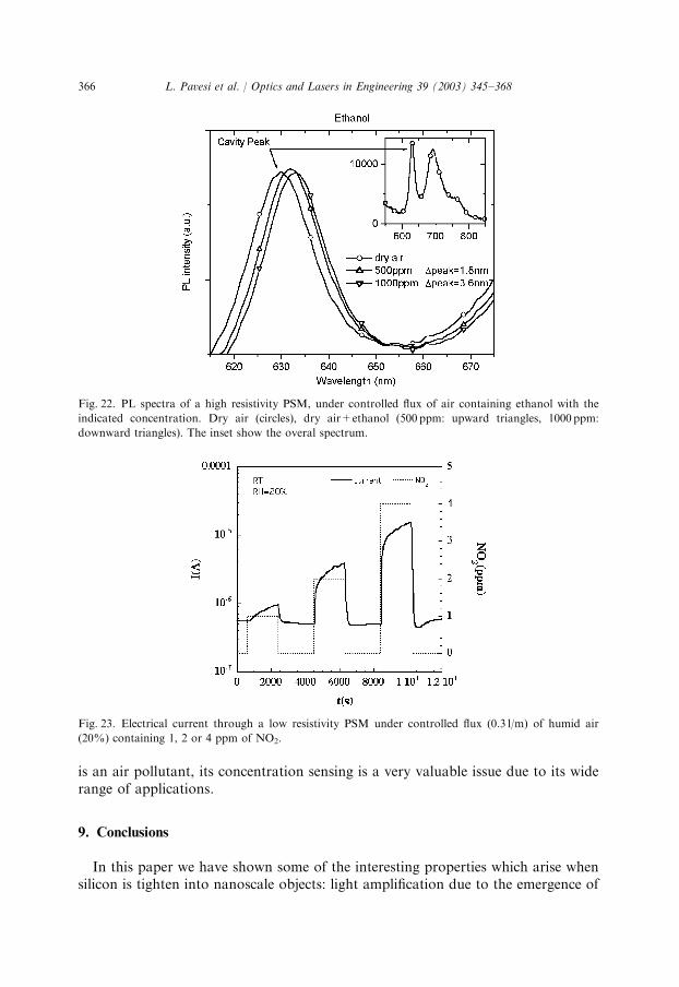
Here we report on experiments which demonstrated the selectivity of the sensorsand posed upper limits to their sensitivity. The sensor is based on porous siliconmicrocavities which have been obtained in a way similar to the one described in Ref.[44]. We aimed to demonstrate the effectiveness of the sensor as detector of NO2, anhazardous air pollutant. In Fig. 21, it is shown the luminescence spectrum fordifferent concentrations of NO2. We can see a significant quenching of theluminescence. However no shift in the spectral features are observed. This contraststo most of the behaviors that this kind of sensor has when exposed to other gases[43]. In Fig. 22 we show the response of our microcavity to the presence of ethanol:no quenching of the luminescence is observed while a clear spectral shift of theluminescence features is measured. In this way a good selectivity of the sensor toNO2 can be inferred. As far as the sensitivity, conductance measurements arereported in Fig. 23. Clearly, the presence of NO2 can be detected down to aconcentration of 1 ppm. Also the current recovers completely to the initial valueafter dry air is restored. The relative response DG=G of the PSM was of 6.6 at 2 ppm.Thus the presence of NO2, in concentrations of the order of few to few tens of ppm,causes (a) PL quenching (b) conduction enhancement (c) no cavity peak-shift. Allthis measurements demonstrate the feasibility of a multiparametric gas sensor able todistinguish and to measure different gas components. In the special case of NO2, as it
Fig. 21. PL spectra of a high resistivity PSM, under controlled flux (0.3 l/m), of dry air (circles), dry
air+NO2 (21 ppm, downward triangles), and back to dry air (upward triangles). Timing of switching of
flux, as well as of spectra acquisition, is indicated in the plot (room temperature).
L. Pavesi et al. / Optics and Lasers in Engineering 39 (2003) 345–368 365
is an air pollutant, its concentration sensing is a very valuable issue due to its widerange of applications.
9. Conclusions
In this paper we have shown some of the interesting properties which arise whensilicon is tighten into nanoscale objects: light amplification due to the emergence of
Fig. 22. PL spectra of a high resistivity PSM, under controlled flux of air containing ethanol with the
indicated concentration. Dry air (circles), dry air+ethanol (500 ppm: upward triangles, 1000 ppm:
downward triangles). The inset show the overal spectrum.
Fig. 23. Electrical current through a low resistivity PSM under controlled flux (0.3 l/m) of humid air
(20%) containing 1, 2 or 4 ppm of NO2.
L. Pavesi et al. / Optics and Lasers in Engineering 39 (2003) 345–368366

radiative interface states, non-linear optical properties due to the quantumconfinement enhanced third order susceptibility, sharp room temperature lumines-cence due to the spatial redistribution of spontaneous emission in an opticalmicrocavity activated by silicon superlattices, selective sensing of poisonous gas dueto the enormous internal surface of porous silicon. Other novel properties crop upwhen silicon is structured in such a way that the propagation of light through it ismodified: beating of disordered slown down photon modes in Fibonacci one-dimensional crystals, modified energy dispersion of photons in two-dimensionalmacroporous silicon. All these novel properties can be engineered to open newperspectives in photonic applications of silicon.
Acknowledgements
The work here reported is the outcomes of numerous collaborations we have. Wethank all the partners of the various institutions who have contributed to theseresults and the various sponsor agencies who have financed our work.
References
[1] Ball P. Nature 2001;409:974.
[2] Pavesi L, Dal Negro L, Mazzoleni C, Franz "o G, Priolo F. Nature 2000;408:440.
[3] Silicon based microphotonics: from basics to applications, Proceedings of the E. Fermi Schools:
Course CXLI, Bisi O, Campisano SU, Pavesi L, Priolo F, editors. Amsterdam: IOS press, 1999.
[4] Bisi O, Ossicini S, Pavesi L. Porous silicon: a quantum sponge structure for silicon based
optoelectronic. Surf Sci Rep 2000;264:1–126.
[5] Wolkin MV, Jorne J, Fauchet PM, Allan G, Delerue C. Phys Rev Lett 1999;82:197–200.
[6] Shaklee KL, Nahaory RE, Leheny RF. J Lumin 1973;7:284–309.
[7] Yariv A. Quantum electronics, 2nd edition.. New York: John Wiley & Sons, Inc., 1975.
[8] Blood P. IEEE J Quantum Electron 2000;36:354–62.
[9] Kirstaedter N, et al. Appl Phys Lett 1996;69:1226–8.
[10] Lingk C, von Plessen G, Feldmann J, Stock K, Arzberger M, Bohm G, Amann MC, Abstreiter G.
Appl Phys Lett 2000;76:3507–9.
[11] Henari FZ, Morgenstern K, Blau WJ, Karavanski VA, Dneprovskii VS. Appl Phys Lett 1995;67:323
and references therein.
[12] Mansoor Sheik-Bahae, Alli a Said, Tai-Huei Wei, David J Hagan, Van Stryland EW. IEEE.
J Quantum Electronics 1990;QE26:760.
[13] Iacona F, Franzo G, Spinella C. J Appl Phys 2000;87:1295 and references therein.
[14] Reitze DH, Zang tR, Wood WmM, Downer MC. J Opt Soc Am B 1990;7:84.
[15] Vijaya Prakash G, Daldosso N, Elena Degoli, Iacona F, Pucker G, Cazzanelli M, Rocca F, Gaburro
Z, Dalba P, Ceretta Moreira E, Pacifici D, Franz "o G, Priolo F, Arcangeli C, Filonov AB, Stefano
Ossicini, Pavesi L. J Nano Sci Nano Tech 2001;1:159.
[16] Reintjes JF, McGroddy JC. Phys Rev Lett 1973;30:901.
[17] Vogel EM, Weber MJ, Krol DM. Phys Chem Glass 1991;32:231.
[18] Chen R, Lin DL, Mendoza B. Phys Rev B 1993;48:11879.
[19] Vijaya Lakshmi S, Shen F, Grebel H. Appl Phys Lett 1997;71:3332.
[20] Vijaya Lakshmi S, George MA, Grebel H. Appl Phys Lett 1997;70:708.
[21] Pucker G, Cazzanelli M, Bellutti P, Gatterer K, Spinella C, Pavesi L. J Appl Phys 2000;88:6044.
L. Pavesi et al. / Optics and Lasers in Engineering 39 (2003) 345–368 367

[22] Mulloni V, Chierchia R, Mazzoleni C, Pucker G, Pavesi L. Phil Mag B 2000;80:705.
[23] Confined electrons and photons, Weisbuch C, Burstein E, editors. Boston: Plenum Press, 1995.
[24] Pavesi L. La Rivista del Nuovo Cimento 1997;20:1.
[25] Pavesi L, Panzarini G, Andreani LC. Phys Rev B 1998;58:15794.
[26] Ossicini S, Degoli E. In: Pavesi L, Buzaneva E, editors. Frontiers of Nano-Optoelectronic Systems.
Dordrecht: Kluwer Academic Publishers, 2000. p. 147–60.
[27] Jannopoulos JD, Meade RD, Winn JN. Photonic crystals: molding the flow of light. Princeton, NJ:
Princeton University Press, 1995.
[28] Lehmann V, G .osele U. Appl Phys Lett 1991;58:856.
[29] F .oll H, Cartensen J, Christophersen M, Hasse G. Phys Stat Sol A 2000;182:7.
[30] Lehmann V, F .oll H. J Electrochem Soc 1990;137:653.
[31] Lehmann V, R .onnenbeck S. J Electrochem Soc 1999;146:2968.
[32] Galli M, et al. Phys Rev Lett, submitted.
[33] Gaburro Z, You H, Babic D. J Appl Phys 1998;84:6345.
[34] Th .onissen M, Billat S, Kr .uger M, et al. J Appl Phys 1996;80:2990.
[35] Th .onissen M, Berger MG, Billat S, et al. Thin Solid Films 1997;297:92.
[36] Anderson PW. Phys Rev 1958;109:1492.
[37] Sorek Y, Reisfeld R, Weiss AM. Chem Phys Lett 1995;244:371.
[38] van Albada MP, Lagendijk A. Phys Rev Lett 1985;55:2692.
[39] Wiersma DS, Bartolini P, Lagendijk A, Righini R. Nature 1997;390:671.
[40] Machida K, Fujita M. Phys Rev B 1986;34:7367.
[41] Rik HJ Kop, Sprik R. Rev Sci Instrum 1995;66:5459.
[42] Arnout Imhof, Willem L Vos, Sprik R, Lagendijk A. Phys Rev Lett 1999;83:2942.
[43] Mulloni V, Pavesi L. Appl Phys Lett 2000;76:2523.
[44] Gaburro Z, Daldosso N, Pavesi L, Faglia G, Baratto C, Sberveglieri G. Appl Phys Lett 2001;
78:3744.
L. Pavesi et al. / Optics and Lasers in Engineering 39 (2003) 345–368368