
Waveguide design, modeling, and optimization: from photonic nanodevices to integrated photonic...
16
Waveguide design, modelling, and optimization – from photonic nano-devices to integrated photonic circuits Michal Bordovský a , Peter Catrysse c , Steven Dods a , Marcio Freitas a , Jackson Klein a , Libor Kotačka b , Velko Tzolov a , Ivan Uzunov a , Jiazong Zhang a , a Optiwave Corp., 7 Capella Court, Ottawa, ON, K2E 7X1, Canada, Tel.: +1 613 224 4700, fax. +1 613 224 4706 b École Polytechnique de Montréal, Montréal, PQ, H3C 3A7 Canada, Tel: +1 514 340 4711 ex. 4489 c Stanford University, Dept. of Electrical Engineering, Stanford, CA 94305 USA, Tel: +1 650 725 1255 ABSTRACT We present the state of the art for commercial design and simulation software in the ‘front end’ of photonic circuit design. One recent advance is to extend the flexibility of the software by using more than one numerical technique on the same optical circuit. There are a number of popular and proven techniques for analysis of photonic devices. Examples of these techniques include the Beam Propagation Method (BPM), the Coupled Mode Theory (CMT), and the Finite Difference Time Domain (FDTD) method. For larger photonic circuits, it may not be practical to analyse the whole circuit by any one of these methods alone, but often some smaller part of the circuit lends itself to at least one of these standard techniques. Later the whole problem can be analysed on a unified platform. This kind of approach can enable analysis for cases that would otherwise be cumbersome, or even impossible. We demonstrate solutions for more complex structures ranging from the sub-component layout, through the entire device characterization, to the mask layout and its editing. We also present recent advances in the above well established techniques. This includes the analysis of nano-particles, metals, and non-linear materials by FDTD, photonic crystal design and analysis, and improved models for high concentration Er/Yb co-doped glass waveguide amplifiers. Keywords: optical waveguides, photonics, optical circuits, nano-optics, numerical simulation 1. INTRODUCTION Recent advances in photonics increase the demand for a well-connected and integrated suite of many simulation and supporting tools. In the design of complicated structures it might be necessary to combine the strengths and advantages of several methods. Further, certain extensive layouts (normally analyzed by a specific tool only) can be advantageously divided into smaller functional parts and analyzed more effectively by means of an advanced tool, e.g. based on a quasi- analytical approach. Our paper deals with certain aspects of so called ‘front-end’ photonic circuit design. We propose an exploitation of specific simulation and designing tools to simplify the simulation process in a flexible way. This can enable the use of different techniques, where simulations by means of any particular tool (e.g. BPM) become cumbersome or even theoretically impossible. For example, in some cases part of a design can be simulated using different approaches, and then later analysed through a unified platform. We also provide a solution for more complex structures ranging from the sub-component layout, through the entire device characterization, to the mask layout and its editing. Based on our recent progress in the field, we are able to provide a solution for layout creation, simulation, and mask editing for problems such as various scattering phenomena (Bragg gratings) followed by standard waveguide devices (couplers, splitters, combiners ...) and their practical applications (sensors, switches). We will discuss bi-directional and certain omni-directional problems. Photonic crystals are obviously recognized as a very specific group of photonic components and special attention has to be paid to them. In Section 2 a few samples simulating third order non-linear
-
Upload
independent -
Category
Documents
-
view
3 -
download
0
Transcript of Waveguide design, modeling, and optimization: from photonic nanodevices to integrated photonic...
Waveguide design, modelling, and optimization – from photonic nano-devices to integrated photonic circuits
Michal Bordovskýa, Peter Catryssec, Steven Dodsa, Marcio Freitasa,
Jackson Kleina, Libor Kotačkab, Velko Tzolova, Ivan Uzunova, Jiazong Zhanga, aOptiwave Corp., 7 Capella Court, Ottawa, ON, K2E 7X1, Canada,
Tel.: +1 613 224 4700, fax. +1 613 224 4706 bÉcole Polytechnique de Montréal, Montréal, PQ, H3C 3A7 Canada,
Tel: +1 514 340 4711 ex. 4489 cStanford University, Dept. of Electrical Engineering, Stanford, CA 94305 USA,
Tel: +1 650 725 1255
ABSTRACT We present the state of the art for commercial design and simulation software in the ‘front end’ of photonic circuit design. One recent advance is to extend the flexibility of the software by using more than one numerical technique on the same optical circuit. There are a number of popular and proven techniques for analysis of photonic devices. Examples of these techniques include the Beam Propagation Method (BPM), the Coupled Mode Theory (CMT), and the Finite Difference Time Domain (FDTD) method. For larger photonic circuits, it may not be practical to analyse the whole circuit by any one of these methods alone, but often some smaller part of the circuit lends itself to at least one of these standard techniques. Later the whole problem can be analysed on a unified platform. This kind of approach can enable analysis for cases that would otherwise be cumbersome, or even impossible. We demonstrate solutions for more complex structures ranging from the sub-component layout, through the entire device characterization, to the mask layout and its editing. We also present recent advances in the above well established techniques. This includes the analysis of nano-particles, metals, and non-linear materials by FDTD, photonic crystal design and analysis, and improved models for high concentration Er/Yb co-doped glass waveguide amplifiers. Keywords: optical waveguides, photonics, optical circuits, nano-optics, numerical simulation
1. INTRODUCTION Recent advances in photonics increase the demand for a well-connected and integrated suite of many simulation and supporting tools. In the design of complicated structures it might be necessary to combine the strengths and advantages of several methods. Further, certain extensive layouts (normally analyzed by a specific tool only) can be advantageously divided into smaller functional parts and analyzed more effectively by means of an advanced tool, e.g. based on a quasi-analytical approach. Our paper deals with certain aspects of so called ‘front-end’ photonic circuit design. We propose an exploitation of specific simulation and designing tools to simplify the simulation process in a flexible way. This can enable the use of different techniques, where simulations by means of any particular tool (e.g. BPM) become cumbersome or even theoretically impossible. For example, in some cases part of a design can be simulated using different approaches, and then later analysed through a unified platform. We also provide a solution for more complex structures ranging from the sub-component layout, through the entire device characterization, to the mask layout and its editing. Based on our recent progress in the field, we are able to provide a solution for layout creation, simulation, and mask editing for problems such as various scattering phenomena (Bragg gratings) followed by standard waveguide devices (couplers, splitters, combiners ...) and their practical applications (sensors, switches). We will discuss bi-directional and certain omni-directional problems. Photonic crystals are obviously recognized as a very specific group of photonic components and special attention has to be paid to them. In Section 2 a few samples simulating third order non-linear
materials, sub-wavelength metallic gratings, and nano-optical devices by the FDTD method will be mentioned. Section 3 has a description of the Plane Wave Expansion (PWE) method for constructing the band structure of photonic crystals. Section 4 shows some realistic examples of the simulation of complex devices and circuits and their various functional combinations (add-drop multiplexers, cascaded switches, AWGs etc.). These examples will also be the best candidates for interactive mask design. In Section 5 we present recent work on modeling high concentration Er/Yb co-doped glass waveguide amplifiers. High-Erbium concentration causes quenching due to uniform and ion-pair upconversion, which results in serious pump-efficiency reduction, and therefore does not permit high gain with a short device length. On the other hand, short length is very desirable in the waveguide form of the amplifier. Er/Yb co-doping is a candidate technical solution to the problem, and so we present improved numerical models for high concentration Er/Yb co-doped glass waveguide amplifiers. Concluding the paper, we would like to point out future paths and what industry currently needs most.
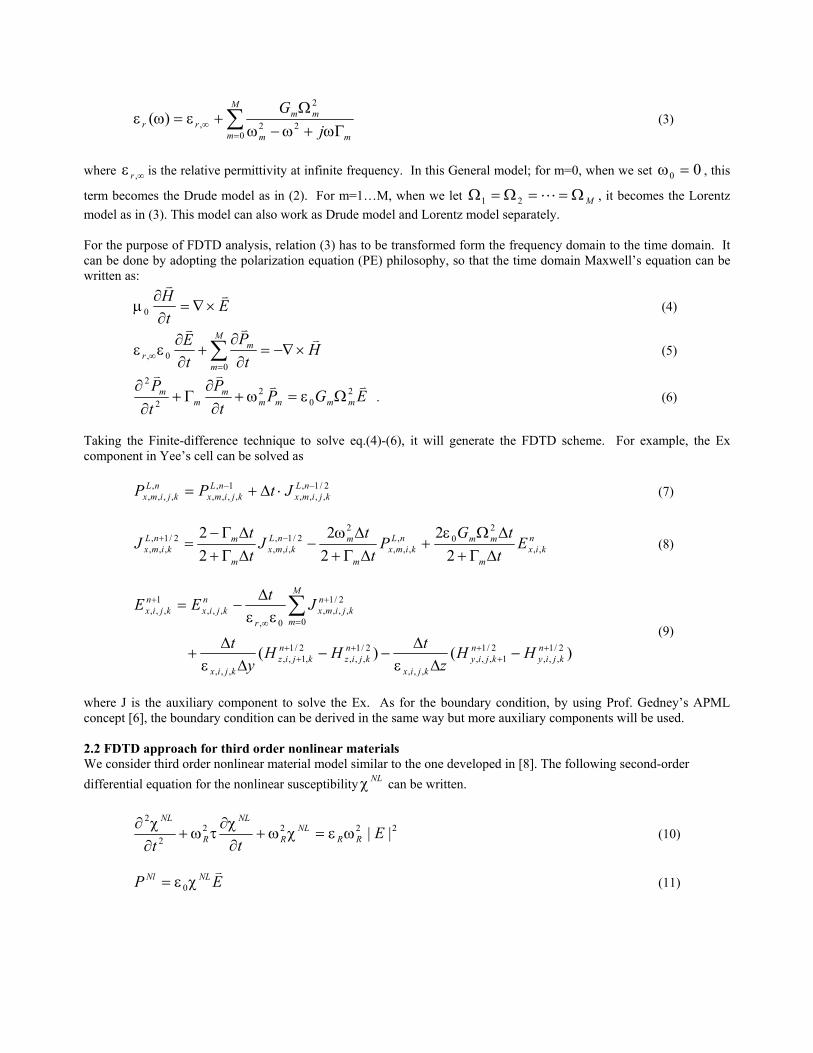
2. EXTENDING THE FDTD METHOD TO NEW APPLICATION AREAS In the past ten years, the FDTD method has been proven to be among the most powerful engineering tools for all areas of electromagnetic simulation. This is due to its unique combination of abilities to model all wave effects such as propagation, scattering, diffraction, reflection and polarization through one analysis. It can also model material anisotropy, dispersion and nonlinearities without any a priori assumption for the wave equation and structure geometries. The most recent research work for the FDTD method can be roughly summarized as four parts:
• Method improvement: these works contain a faster simulation scheme [1], high-order FDTD schemes [2], unconditional stable schemes [3] and alternating mesh scheme [4].
• Boundary condition: PML [5] and APML [6]. • Extending FDTD method to new material models: nonlinear material model, dispersive material model and
quantum materials. • Extending FDTD to new advanced application areas such as biophotonics, biomedical, and nano structures.
Here we present several case studies where the FDTD method is used in the analysis of optical properties of metal layers, four-wave mixing, photonic crystal fibers and nano-particles. 2.1 FDTD approach for optical metallic material The significant advantage of the FDTD method is the great variety of materials that can be consistently modeled within the FDTD context. The metallic material which couples to the Maxwell’s equation is the so-called Lorentz-Drude model, which is described in reference [7]. Up to authors’ knowledge, it is the first time that this advanced optical metallic material model has been developed by FDTD simulation. The Drude dispersive model for surface plasmon is written in the frequency domain as:
20
2
1)(ω−Γω
Ω+=ωε
jpf
r ; (1)
and the Lorentz Model as:
∑= Γω+ω−ω
ω=ωε
M
m mm
pmbr j
G
122
2
)( (2)
where is the plasma frequency, is the number of oscillators with frequency and lifetime pω m mω mΓ/1 ,
pmp G ω=Ω is the plasma frequency as associated with intraband transitions with oscillator strength and
damping constant Γ . The above Lorentz and Drude Model can be expressed as more general equation: 0G
0
∑=
∞ Γω+ω−ωΩ
+ε=ωεM
m mm
mmrr j
G0
22
2
,)( (3)
where is the relative permittivity at infinite frequency. In this General model; for m=0, when we set ∞ε ,r 00 =ω , this
term becomes the Drude model as in (2). For m=1…M, when we let MΩ==Ω=Ω L21 , it becomes the Lorentz model as in (3). This model can also work as Drude model and Lorentz model separately. For the purpose of FDTD analysis, relation (3) has to be transformed form the frequency domain to the time domain. It can be done by adopting the polarization equation (PE) philosophy, so that the time domain Maxwell’s equation can be written as:
Et
H vv
×∇=∂
∂µ0 (4)
∑=
∞ ×−∇=∂
∂+
∂∂
εεM
m
mr H
tP
tE
00,
vvv
(5)
EGPt
PtP
mmmmm
mm
vvvv
20
22
2
Ωε=ω+∂
∂Γ+
∂∂
. (6)
Taking the Finite-difference technique to solve eq.(4)-(6), it will generate the FDTD scheme. For example, the Ex component in Yee’s cell can be solved as
2/1,,,,,
1,,,,,
,,,,,
−− ⋅∆+= nLkjimx
nLkjimx
nLkjimx JtPP (7)
nkix
m
mmnLkimx
m
mnLkimx
m
mnLkimx E
ttG
Pt
tJ
tt
J ,,
20,
,,,
22/1,
,,,2/1,
,,, 22
22
22
∆Γ+∆Ωε
+∆Γ+
∆ω−
∆Γ+∆Γ−
= −+ (8)
)()( 2/1,,,
2/11,,,
,,,
2/1,,,
2/1,1,,
,,,
0
2/1,,,,
0,,,,
1,,,
+++
+++
=
+
∞
+
−∆ε
∆−−
∆ε∆
+
εε∆
−= ∑
nkjiy
nkjiy
kjix
nkjiz
nkjiz
kjix
M
m
nkjimx
r
nkjix
nkjix
HHz
tHHy
t
JtEE (9)
where J is the auxiliary component to solve the Ex. As for the boundary condition, by using Prof. Gedney’s APML concept [6], the boundary condition can be derived in the same way but more auxiliary components will be used. 2.2 FDTD approach for third order nonlinear materials We consider third order nonlinear material model similar to the one developed in [8]. The following second-order differential equation for the nonlinear susceptibility χ can be written. NL
22222
2
|| Ett RR
NLR
NL
R
NL
ωε=χω+∂χ∂
τω+∂χ∂
(10)
EP NLNl v
χε= 0 (11)
where is nonlinear permittivity, τ is the photo response time, and Rε Rω is the resonant frequency. By using the finite-difference technique to equation (10) and Maxwell’s equations, the following FDTD scheme can be derived: (Ey components FDTD equation only is shown).
)||(22
22 ,
,2
22/1,
,2/1,
,nNL
kiyRR
RnNLki
R
RnNLki E
tt
tt
χ−ε∆Γ+
∆ω+σ
∆Γ+∆Γ−
=σ −+ (12)
2/1,
,,
,1,
,++ ∆+= nNL
kinNL
kinNL
ki tσχχ (13)
)()(
1
)()(
1)(
)(
2/1,1,
2/1,,1,
,0
2/11,,
2/1,,1,
,0,,1,
,0
,,01
,,
+−
++
+−
+++
+
−∆∆
+−
−∆∆
++
+
+=
kizn
kiznNLkiL
nkix
nkixnNL
kiL
nkiynNL
kiL
nNLkiLn
kiy
HHxt
HHztEE
χεε
χεεχεεχεε
(14)
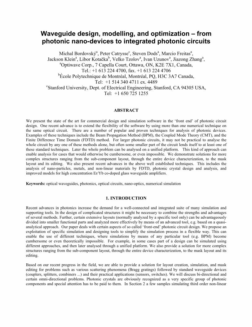
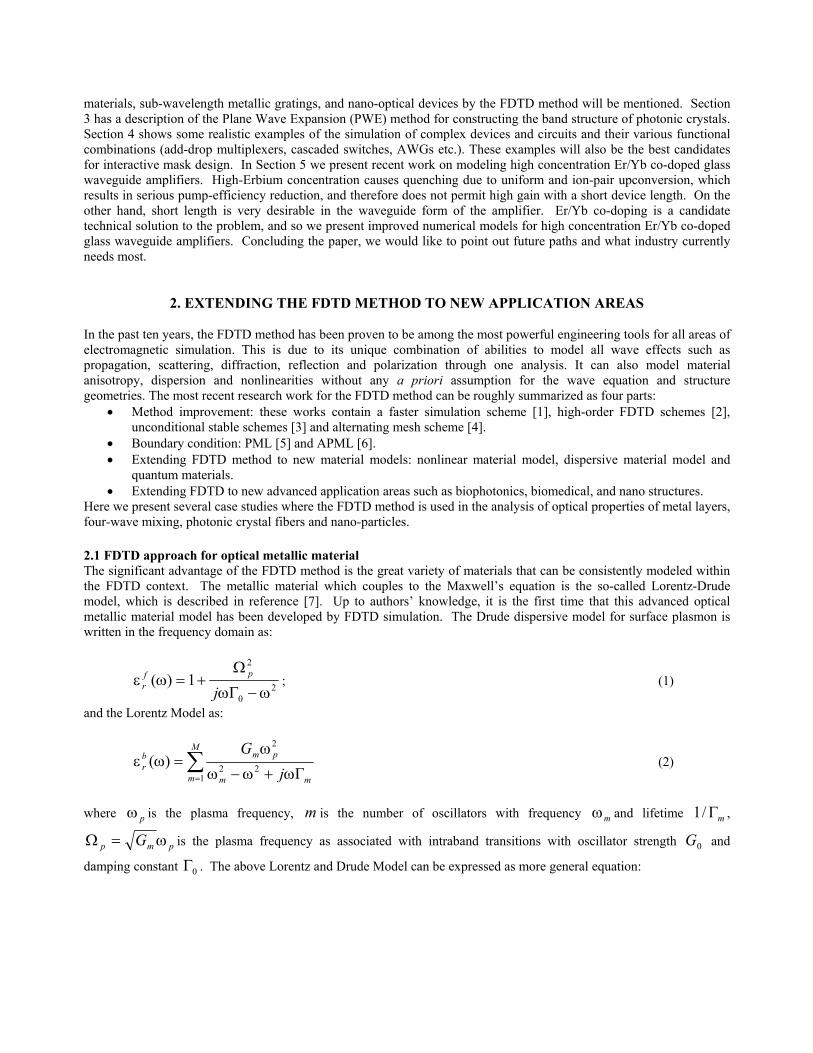
where σ is the auxiliary component to solve Ey. 2.3 Numerical samples 2.3.1 Metallic grating Metallic structures with typical dimensions below the wavelength of light are expected to show local enhancement of the electromagnetic field strength, which may affect the field effect dramatically. In this sample we show a metallic grating structure. Figure 1 shows the power transmittance for a metallic grating with different material. As you can see, the different metal material will shift the filter’s range. Figure 2 is for the Al grating with TiN coating in the SiO2 wafer.
0.4 0.5 0.6 0.7 0.8 0.9 1.0 1.1-0.1
0.0
0.1
0.2
0.3
0.4
0.5
0.6
0.7
0.8
0.9
Perfect conductor Ag Al
trans
mitt
ance
(TE)
Wavelength (µm)0.4 0.5 0.6 0.7 0.8 0.9 1.0 1.1
-0.2
-0.1
0.0
0.1
0.2
0.3
0.4
0.5
SiO2
TiNAl
TE TM
Y Ax
is T
itle
Wavelength(µm)
Figure 1. Power transmittance of metallic grating layout. Figure 2. Power transmittance for a metallic grating with TiN coating.
2.3.2 Four Wave Mixing effect in third order nonlinear material This sample shows four-wave mixing in third order nonlinear material (as described in section 2). The layout had three linear input channels with modal input at wavelengths 1.4µm, 1.55 µm, and 1.6 µm. The input waves are coupled to a region with nonlinear Raman material with photo response time of 5.0e-15s. The non-linear permittivity is 1.32e-12, and

the resonant frequency is 1.25 rad/s. Three observation points are set to monitor the FWM effect as shown in Figure 3. The spectral analysis in these three observation points is shown in Figure 4.
1.0 1.2 1.4 1.6 1.8 2.0 2.20.0
4.0x10⁵
8.0x10⁵
Point 1 at (-1.2,0, 6)
Ey (V
/m)
1.0 1.2 1.4 1.6 1.8 2.0 2.20.0
4.0x10⁵
8.0x10⁵
Point 2 at (1.2,0,6)
Ey (V
/m)
1.0 1.2 1.4 1.6 1.8 2.0 2.20.0
4.0x10⁵
8.0x10⁵
Point 1 at (0,0,6)
Ey (V
/m)
Wavelength (µm)
Figure 3. FWM layout Figure 4. Spectrum for FWM
2.3.3 Fiber to photonic crystal fiber coupling Most recently the Photonic Crystal Fiber (PCF) has become a heavily researched area. The modal and the band-diagram analysis can be performed by traditional means. However, for complex wave propagation, coupling, and defect simulation, FDTD method is considered to be the most appropriate method. Figure 5 shows butt coupling between the traditional fiber to a photonic crystal fiber. Our FDTD calculations can predict the coupling efficiency as a function of the design parameter. The developed PCF mode is shown in Figure 6.
Fiber
PCF
Figure 5 A Fiber to PCF coupler
Figure 6. Calculated PCF fiber modal field distribution simulated with OptiFDTD™.
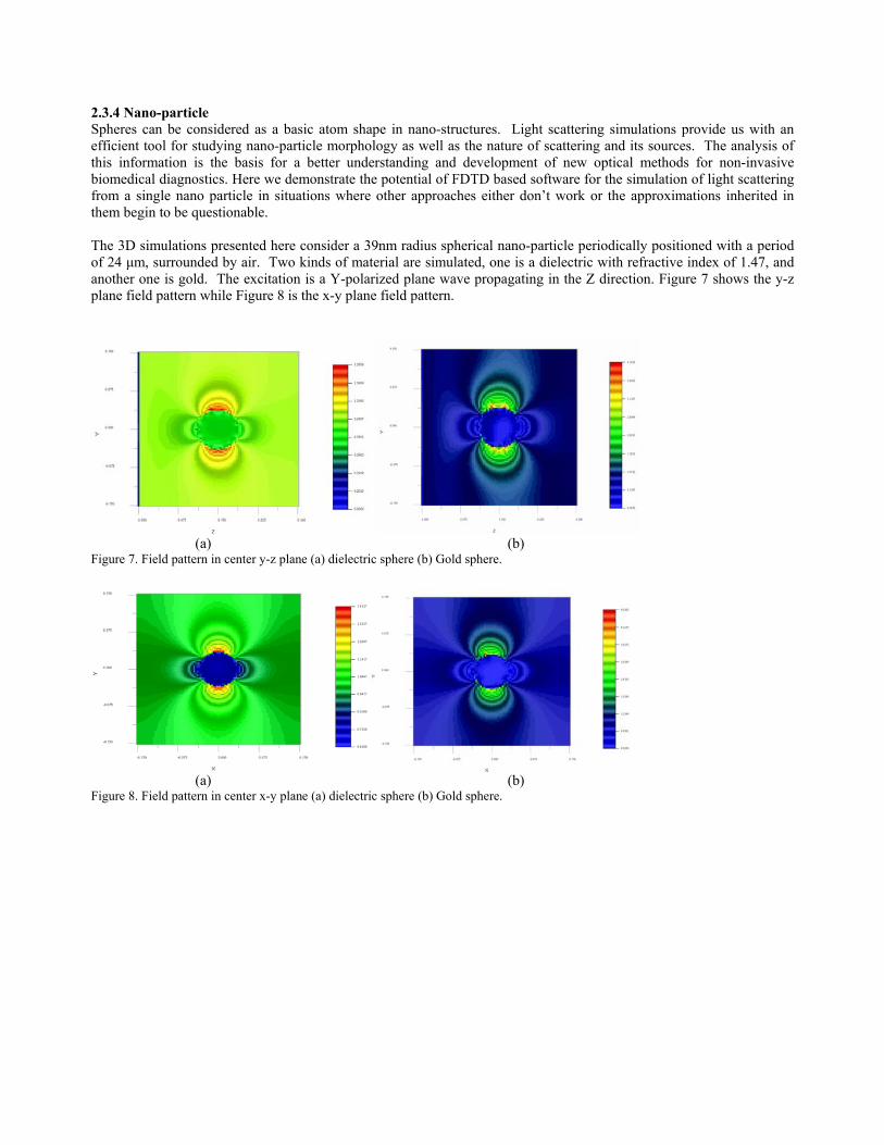
2.3.4 Nano-particle Spheres can be considered as a basic atom shape in nano-structures. Light scattering simulations provide us with an efficient tool for studying nano-particle morphology as well as the nature of scattering and its sources. The analysis of this information is the basis for a better understanding and development of new optical methods for non-invasive biomedical diagnostics. Here we demonstrate the potential of FDTD based software for the simulation of light scattering from a single nano particle in situations where other approaches either don’t work or the approximations inherited in them begin to be questionable. The 3D simulations presented here consider a 39nm radius spherical nano-particle periodically positioned with a period of 24 µm, surrounded by air. Two kinds of material are simulated, one is a dielectric with refractive index of 1.47, and another one is gold. The excitation is a Y-polarized plane wave propagating in the Z direction. Figure 7 shows the y-z plane field pattern while Figure 8 is the x-y plane field pattern.
(a) (b) Figure 7. Field pattern in center y-z plane (a) dielectric sphere (b) Gold sphere.
(a) (b)
Figure 8. Field pattern in center x-y plane (a) dielectric sphere (b) Gold sphere.
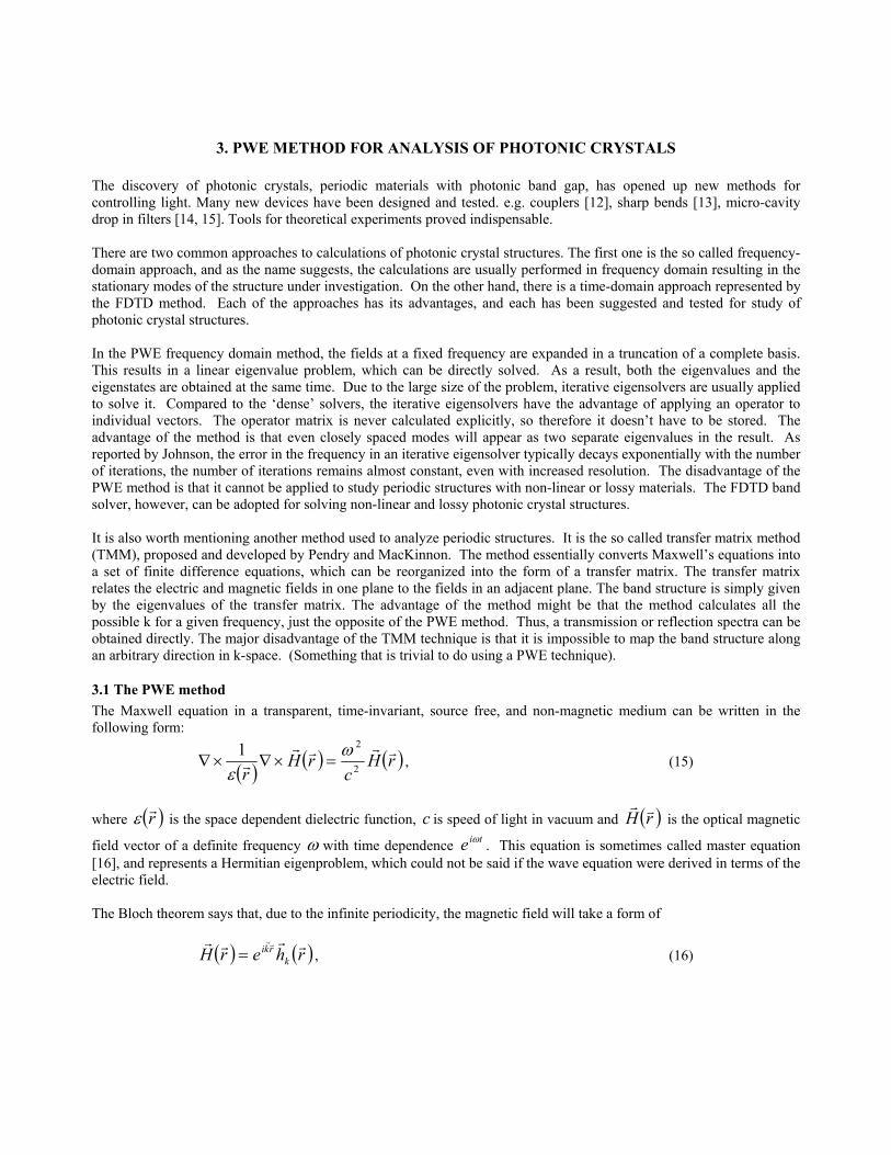
3. PWE METHOD FOR ANALYSIS OF PHOTONIC CRYSTALS
The discovery of photonic crystals, periodic materials with photonic band gap, has opened up new methods for controlling light. Many new devices have been designed and tested. e.g. couplers [12], sharp bends [13], micro-cavity drop in filters [14, 15]. Tools for theoretical experiments proved indispensable. There are two common approaches to calculations of photonic crystal structures. The first one is the so called frequency-domain approach, and as the name suggests, the calculations are usually performed in frequency domain resulting in the stationary modes of the structure under investigation. On the other hand, there is a time-domain approach represented by the FDTD method. Each of the approaches has its advantages, and each has been suggested and tested for study of photonic crystal structures. In the PWE frequency domain method, the fields at a fixed frequency are expanded in a truncation of a complete basis. This results in a linear eigenvalue problem, which can be directly solved. As a result, both the eigenvalues and the eigenstates are obtained at the same time. Due to the large size of the problem, iterative eigensolvers are usually applied to solve it. Compared to the ‘dense’ solvers, the iterative eigensolvers have the advantage of applying an operator to individual vectors. The operator matrix is never calculated explicitly, so therefore it doesn’t have to be stored. The advantage of the method is that even closely spaced modes will appear as two separate eigenvalues in the result. As reported by Johnson, the error in the frequency in an iterative eigensolver typically decays exponentially with the number of iterations, the number of iterations remains almost constant, even with increased resolution. The disadvantage of the PWE method is that it cannot be applied to study periodic structures with non-linear or lossy materials. The FDTD band solver, however, can be adopted for solving non-linear and lossy photonic crystal structures. It is also worth mentioning another method used to analyze periodic structures. It is the so called transfer matrix method (TMM), proposed and developed by Pendry and MacKinnon. The method essentially converts Maxwell’s equations into a set of finite difference equations, which can be reorganized into the form of a transfer matrix. The transfer matrix relates the electric and magnetic fields in one plane to the fields in an adjacent plane. The band structure is simply given by the eigenvalues of the transfer matrix. The advantage of the method might be that the method calculates all the possible k for a given frequency, just the opposite of the PWE method. Thus, a transmission or reflection spectra can be obtained directly. The major disadvantage of the TMM technique is that it is impossible to map the band structure along an arbitrary direction in k-space. (Something that is trivial to do using a PWE technique).
3.1 The PWE method The Maxwell equation in a transparent, time-invariant, source free, and non-magnetic medium can be written in the following form:
( ) ( ) ( )rHc
rHr
rrrrr 2
21 ωε
=×∇×∇ , (15)
where ( )rrε is the space dependent dielectric function, c is speed of light in vacuum and ( )rH vr
is the optical magnetic
field vector of a definite frequency ω with time dependence e . This equation is sometimes called master equation [16], and represents a Hermitian eigenproblem, which could not be said if the wave equation were derived in terms of the electric field.
tiω
The Bloch theorem says that, due to the infinite periodicity, the magnetic field will take a form of
( ) ( )rherH krki rrrr rr
= , (16)
where ( ) ( )Rrhrhrrrrr
+= for all combinations of lattice vectors Rr
. Thus we end up with the master equation in operator form:
( ) ( ) ( ) kk hc
hkir
kirrr
rr
2
21 ωε
=×
+∇×+∇ (17)
This is the fundamental equation, which needs to be solved. The equation is transformed into a finite problem by expanding the magnetic field in a finite basis of simple plane waves. Different approaches can be explored to solve the final discretized problem, e.g. [17] and [18]. The result of solving the discretized problem is the dispersion relationship between the frequencies of the modes and wave vector
kr
, usually plotted in the form of a band diagram. The band diagram of a photonic band structure of a rectangular 2D lattice is shown in Fig. 9.
Figure 9. Photonic band structure of a rectangular 2D lattice. The dielectric columns (permittivity =3.1*3.1=9.6) in air have radius of 0.2a, where a is the lattice constant
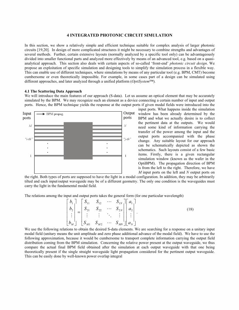
4 INTEGRATED PHOTONIC CIRCUIT SIMULATION
In this section, we show a relatively simple and efficient technique suitable for complex analysis of larger photonic circuits [19,20]. In design of more complicated structures it might be necessary to combine strengths and advantages of several methods. Further, certain extensive layouts (normally analyzed by a specific tool only) can be advantageously divided into smaller functional parts and analyzed more effectively by means of an advanced tool, e.g. based on a quasi-analytical approach. This section also deals with certain aspects of so-called ‘front-end’ photonic circuit design. We propose an exploitation of specific simulation and designing tools to simplify the simulation process in a flexible way. This can enable use of different techniques, where simulations by means of any particular tool (e.g. BPM, CMT) become cumbersome or even theoretically impossible. For example, in some cases part of a design can be simulated using different approaches, and later analyzed through a unified platform (OptiSystem™). 4.1 The Scattering Data Approach We will introduce the main features of our approach (S-data). Let us assume an optical element that may be accurately simulated by the BPM. We may recognize such an element as a device connecting a certain number of input and output ports. Hence, the BPM technique yields the response at the output ports if given modal fields were introduced into the
input ports. What happens inside the simulation window has been already determined by the BPM and what we actually desire is to collect the pertinent data at the outputs. We would need some kind of information carrying the transfer of the power among the input and the output ports accompanied with the phase change. Any suitable layout for our approach can be schematically depicted as shown the schematics. Such layouts consist of a few basic items. Firstly, there is a given rectangular simulation window (known as the wafer in the OptiBPM). The propagation direction of BPM is from the left to the right. Therefore, we have M input ports on the left and N output ports on
the right. Both types of ports are supposed to have the light in a modal configuration. In addition, they may be arbitrarily tilted and each input/output waveguide may be of a different geometry. The only one condition is the waveguides must carry the light in the fundamental modal field. The relations among the input and output ports takes the general form (for one particular wavelength)
=
NMNMM
N
N
M a
aa
SSS
SSSSSS
b
bb
M
L
MOMM
L
L
M2
1
21
22221
11211
2
1
.
(18)
We use the following relations to obtain the desired S-data elements. We are searching for a response on a unitary input modal field (unitary means the unit amplitude and zero phase additional advance of the modal field). We have to use the following approximation, because it would be cumbersome to transport complete information carrying the output field distribution coming from the BPM simulation. Concerning the relative power present at the output waveguide, we thus compare the actual final BPM field obtained after the simulation at each output waveguide with that one being theoretically present if the single straight waveguide light propagation considered for the pertinent output waveguide. This can be easily done by well-known power overlap integral
∫∫∫
ΩΩ
Ω
∗
=dxEdxE
dxEEP 2
22
1
2
21, (19)
where one field is the BPM one, while the second is the modal field distribution of output waveguide (the asterisk means the complex conjugated field). The denominator has the product of the two integrals and ensures the normalization of the overlap integral from 0 to 1. means the integration region. The response with respect to the cumulated phase delay is then given by (both real and imaginary part)
Ω
[ ])(exp 0 wgLknjPb θ+−= , (20)
where λπ /2=k , n0 is the reference index, L is the propagation length. Finally, wgθ is an additional angle related to the BPM propagation. Sometimes in one BPM calculation more than one reference index will be used. There may be regions having different reference indices. If more then one region appears in the layout, we have to characterize these regions separately by particular lengths and reference indices and the phase delay term in (20) must be replaced accordingly as shown schematically in Eq. (21)
Lkn0
∑⇒r
rr LnLn0 , (21)
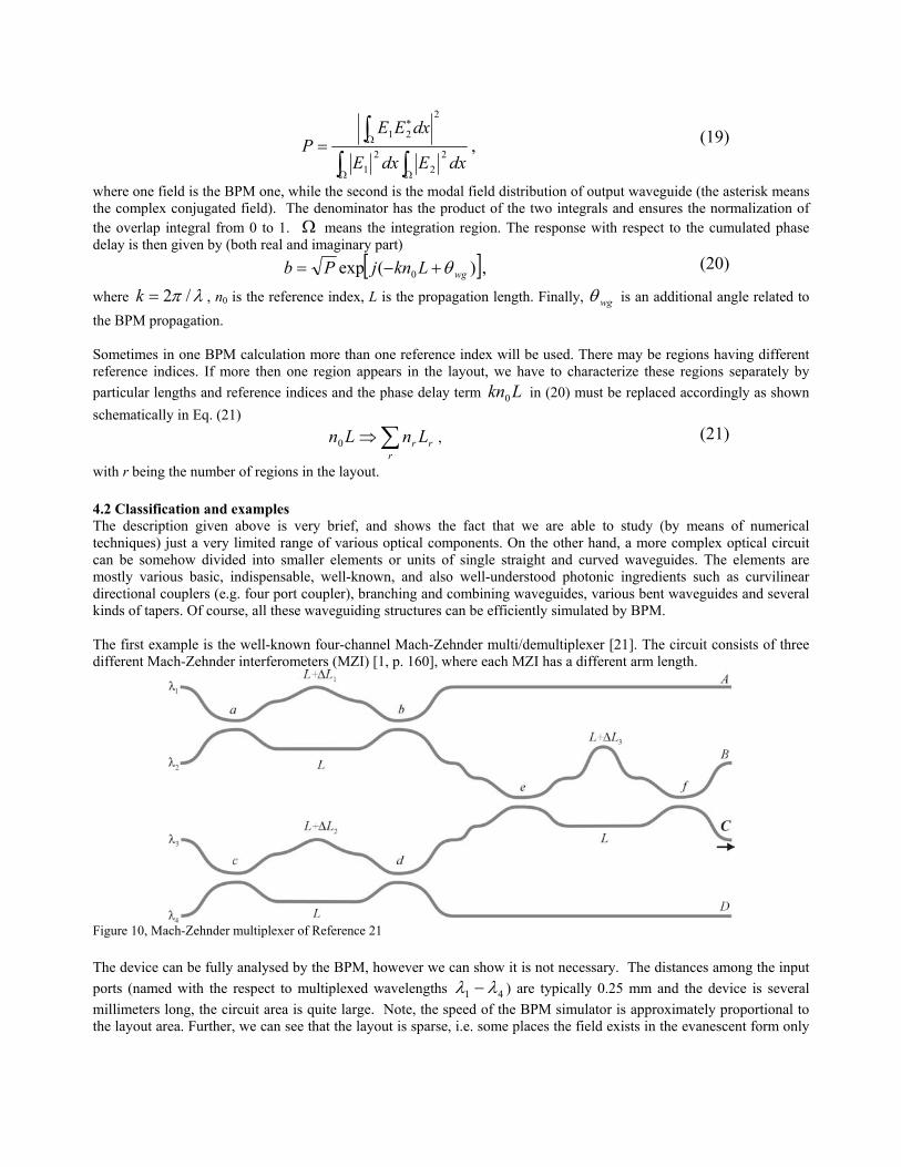
with r being the number of regions in the layout. 4.2 Classification and examples The description given above is very brief, and shows the fact that we are able to study (by means of numerical techniques) just a very limited range of various optical components. On the other hand, a more complex optical circuit can be somehow divided into smaller elements or units of single straight and curved waveguides. The elements are mostly various basic, indispensable, well-known, and also well-understood photonic ingredients such as curvilinear directional couplers (e.g. four port coupler), branching and combining waveguides, various bent waveguides and several kinds of tapers. Of course, all these waveguiding structures can be efficiently simulated by BPM. The first example is the well-known four-channel Mach-Zehnder multi/demultiplexer [21]. The circuit consists of three different Mach-Zehnder interferometers (MZI) [1, p. 160], where each MZI has a different arm length.
Figure 10, Mach-Zehnder multiplexer of Reference 21
The device can be fully analysed by the BPM, however we can show it is not necessary. The distances among the input ports (named with the respect to multiplexed wavelengths 41 λλ − ) are typically 0.25 mm and the device is several millimeters long, the circuit area is quite large. Note, the speed of the BPM simulator is approximately proportional to the layout area. Further, we can see that the layout is sparse, i.e. some places the field exists in the evanescent form only
and is negligible. Running the simulation through these places is inefficient, however we cannot exclude these “dead places” from the rectangular simulation window.
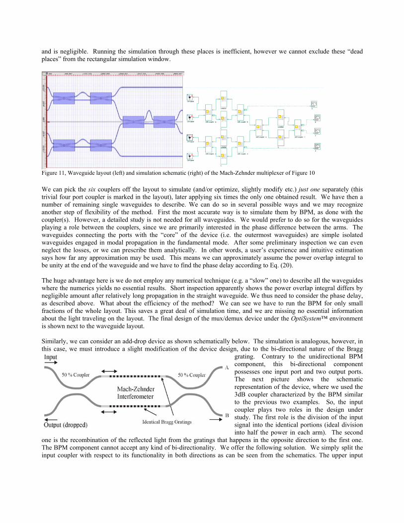
Figure 11, Waveguide layout (left) and simulation schematic (right) of the Mach-Zehnder multiplexer of Figure 10 We can pick the six couplers off the layout to simulate (and/or optimize, slightly modify etc.) just one separately (this trivial four port coupler is marked in the layout), later applying six times the only one obtained result. We have then a number of remaining single waveguides to describe. We can do so in several possible ways and we may recognize another step of flexibility of the method. First the most accurate way is to simulate them by BPM, as done with the coupler(s). However, a detailed study is not needed for all waveguides. We would prefer to do so for the waveguides playing a role between the couplers, since we are primarily interested in the phase difference between the arms. The waveguides connecting the ports with the “core” of the device (i.e. the outermost waveguides) are simple isolated waveguides engaged in modal propagation in the fundamental mode. After some preliminary inspection we can even neglect the losses, or we can prescribe them analytically. In other words, a user’s experience and intuitive estimation says how far any approximation may be used. This means we can approximately assume the power overlap integral to be unity at the end of the waveguide and we have to find the phase delay according to Eq. (20). The huge advantage here is we do not employ any numerical technique (e.g. a “slow” one) to describe all the waveguides where the numerics yields no essential results. Short inspection apparently shows the power overlap integral differs by negligible amount after relatively long propagation in the straight waveguide. We thus need to consider the phase delay, as described above. What about the efficiency of the method? We can see we have to run the BPM for only small fractions of the whole layout. This saves a great deal of simulation time, and we are missing no essential information about the light traveling on the layout. The final design of the mux/demux device under the OptiSystem™ environment is shown next to the waveguide layout. Similarly, we can consider an add-drop device as shown schematically below. The simulation is analogous, however, in this case, we must introduce a slight modification of the device design, due to the bi-directional nature of the Bragg
grating. Contrary to the unidirectional BPM component, this bi-directional component possesses one input port and two output ports. The next picture shows the schematic representation of the device, where we used the 3dB coupler characterized by the BPM similar to the previous two examples. So, the input coupler plays two roles in the design under study. The first role is the division of the input signal into the identical portions (ideal division into half the power in each arm). The second
one is the recombination of the reflected light from the gratings that happens in the opposite direction to the first one. The BPM component cannot accept any kind of bi-directionality. We offer the following solution. We simply split the input coupler with respect to its functionality in both directions as can be seen from the schematics. The upper input
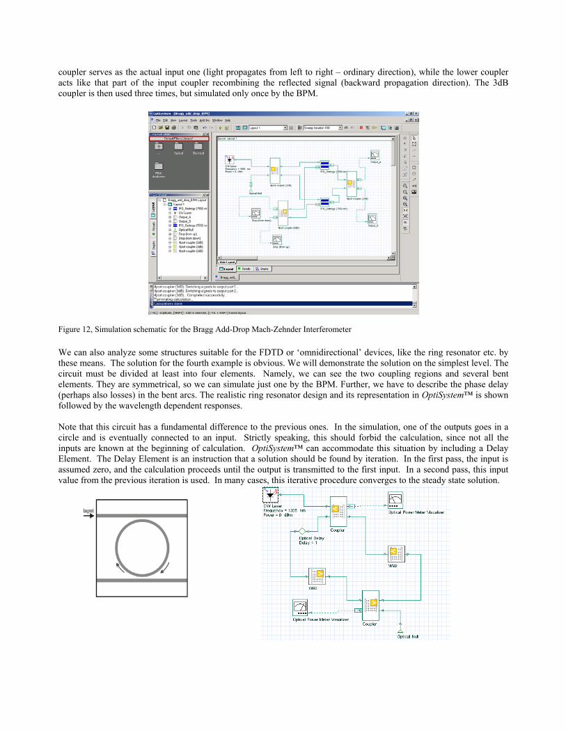
coupler serves as the actual input one (light propagates from left to right – ordinary direction), while the lower coupler acts like that part of the input coupler recombining the reflected signal (backward propagation direction). The 3dB coupler is then used three times, but simulated only once by the BPM.
Figure 12, Simulation schematic for the Bragg Add-Drop Mach-Zehnder Interferometer We can also analyze some structures suitable for the FDTD or ‘omnidirectional’ devices, like the ring resonator etc. by these means. The solution for the fourth example is obvious. We will demonstrate the solution on the simplest level. The circuit must be divided at least into four elements. Namely, we can see the two coupling regions and several bent elements. They are symmetrical, so we can simulate just one by the BPM. Further, we have to describe the phase delay (perhaps also losses) in the bent arcs. The realistic ring resonator design and its representation in OptiSystem™ is shown followed by the wavelength dependent responses. Note that this circuit has a fundamental difference to the previous ones. In the simulation, one of the outputs goes in a circle and is eventually connected to an input. Strictly speaking, this should forbid the calculation, since not all the inputs are known at the beginning of calculation. OptiSystem™ can accommodate this situation by including a Delay Element. The Delay Element is an instruction that a solution should be found by iteration. In the first pass, the input is assumed zero, and the calculation proceeds until the output is transmitted to the first input. In a second pass, this input value from the previous iteration is used. In many cases, this iterative procedure converges to the steady state solution.
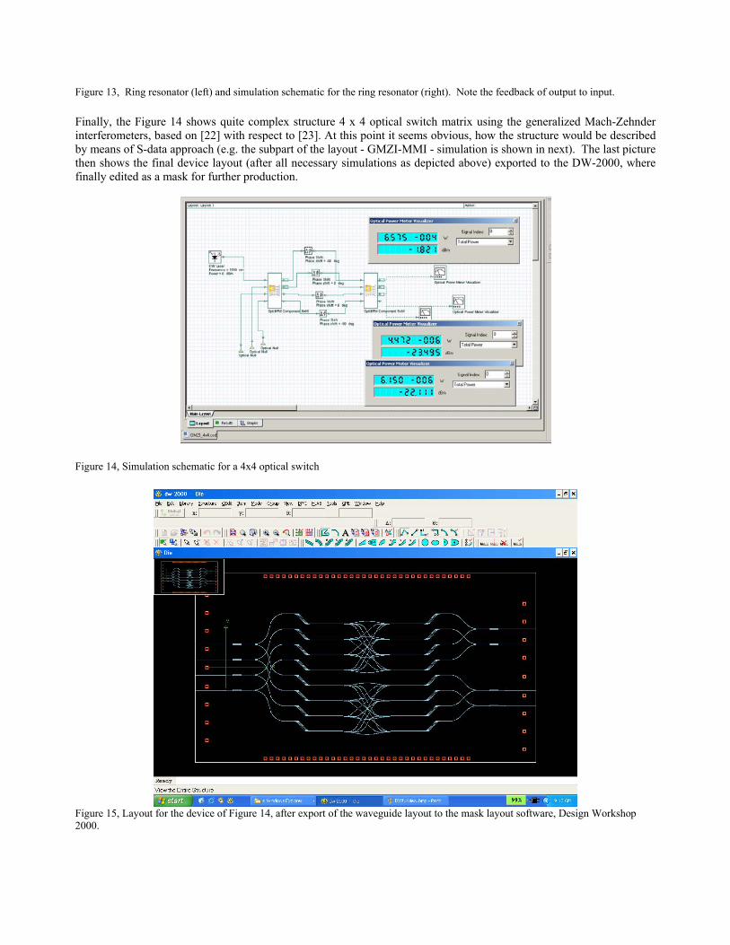
Figure 13, Ring resonator (left) and simulation schematic for the ring resonator (right). Note the feedback of output to input. Finally, the Figure 14 shows quite complex structure 4 x 4 optical switch matrix using the generalized Mach-Zehnder interferometers, based on [22] with respect to [23]. At this point it seems obvious, how the structure would be described by means of S-data approach (e.g. the subpart of the layout - GMZI-MMI - simulation is shown in next). The last picture then shows the final device layout (after all necessary simulations as depicted above) exported to the DW-2000, where finally edited as a mask for further production.
Figure 14, Simulation schematic for a 4x4 optical switch
Figure 15, Layout for the device of Figure 14, after export of the waveguide layout to the mask layout software, Design Workshop 2000.
5. GAIN CHARACTERISTICS IN HIGH-CONCENTRATION ER3+/YB3+ CODOPED GLASS
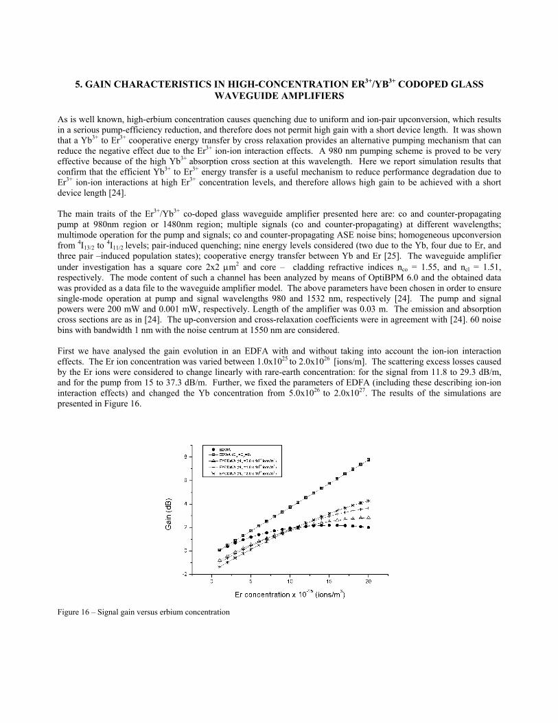
WAVEGUIDE AMPLIFIERS As is well known, high-erbium concentration causes quenching due to uniform and ion-pair upconversion, which results in a serious pump-efficiency reduction, and therefore does not permit high gain with a short device length. It was shown that a Yb3+ to Er3+ cooperative energy transfer by cross relaxation provides an alternative pumping mechanism that can reduce the negative effect due to the Er3+ ion-ion interaction effects. A 980 nm pumping scheme is proved to be very effective because of the high Yb3+ absorption cross section at this wavelength. Here we report simulation results that confirm that the efficient Yb3+ to Er3+ energy transfer is a useful mechanism to reduce performance degradation due to Er3+ ion-ion interactions at high Er3+ concentration levels, and therefore allows high gain to be achieved with a short device length [24]. The main traits of the Er3+/Yb3+ co-doped glass waveguide amplifier presented here are: co and counter-propagating pump at 980nm region or 1480nm region; multiple signals (co and counter-propagating) at different wavelengths; multimode operation for the pump and signals; co and counter-propagating ASE noise bins; homogeneous upconversion
from 4I13/2 to 4I11/2 levels; pair-induced quenching; nine energy levels considered (two due to the Yb, four due to Er, and three pair –induced population states); cooperative energy transfer between Yb and Er [25]. The waveguide amplifier under investigation has a square core 2x2 µm2 and core – cladding refractive indices nco = 1.55, and ncl = 1.51, respectively. The mode content of such a channel has been analyzed by means of OptiBPM 6.0 and the obtained data was provided as a data file to the waveguide amplifier model. The above parameters have been chosen in order to ensure single-mode operation at pump and signal wavelengths 980 and 1532 nm, respectively [24]. The pump and signal powers were 200 mW and 0.001 mW, respectively. Length of the amplifier was 0.03 m. The emission and absorption cross sections are as in [24]. The up-conversion and cross-relaxation coefficients were in agreement with [24]. 60 noise bins with bandwidth 1 nm with the noise centrum at 1550 nm are considered. First we have analysed the gain evolution in an EDFA with and without taking into account the ion-ion interaction effects. The Er ion concentration was varied between 1.0x1025 to 2.0x1026 [ions/m]. The scattering excess losses caused by the Er ions were considered to change linearly with rare-earth concentration: for the signal from 11.8 to 29.3 dB/m, and for the pump from 15 to 37.3 dB/m. Further, we fixed the parameters of EDFA (including these describing ion-ion interaction effects) and changed the Yb concentration from 5.0x1026 to 2.0x1027. The results of the simulations are presented in Figure 16.
Figure 16 – Signal gain versus erbium concentration
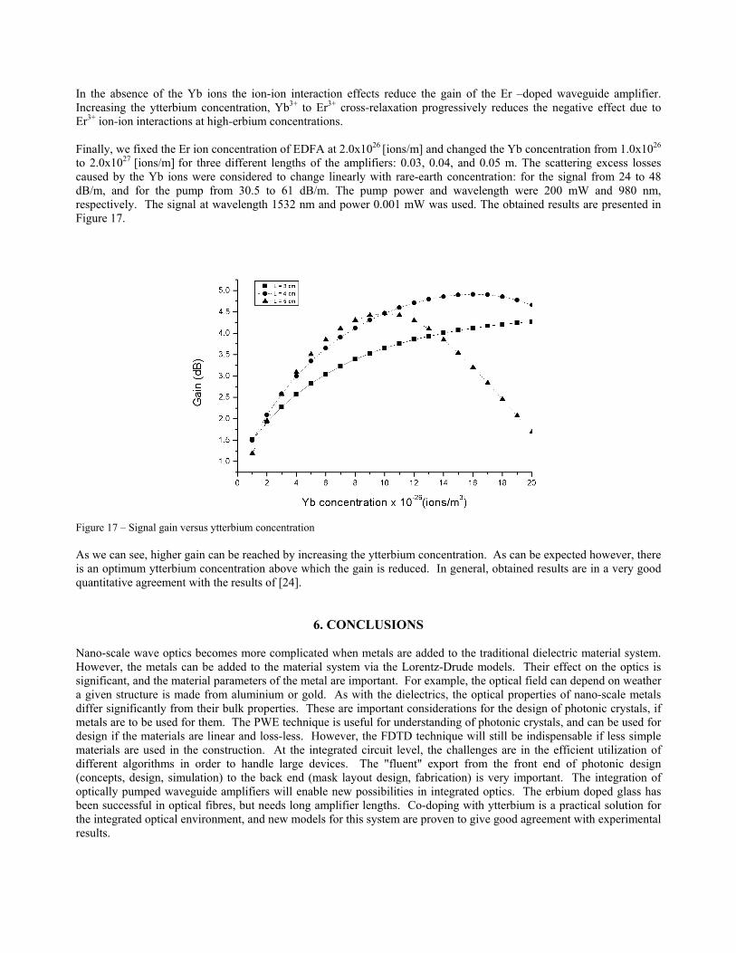
In the absence of the Yb ions the ion-ion interaction effects reduce the gain of the Er –doped waveguide amplifier. Increasing the ytterbium concentration, Yb3+ to Er3+ cross-relaxation progressively reduces the negative effect due to Er3+ ion-ion interactions at high-erbium concentrations. Finally, we fixed the Er ion concentration of EDFA at 2.0x1026 [ions/m] and changed the Yb concentration from 1.0x1026
to 2.0x1027 [ions/m] for three different lengths of the amplifiers: 0.03, 0.04, and 0.05 m. The scattering excess losses caused by the Yb ions were considered to change linearly with rare-earth concentration: for the signal from 24 to 48 dB/m, and for the pump from 30.5 to 61 dB/m. The pump power and wavelength were 200 mW and 980 nm, respectively. The signal at wavelength 1532 nm and power 0.001 mW was used. The obtained results are presented in Figure 17.
Figure 17 – Signal gain versus ytterbium concentration As we can see, higher gain can be reached by increasing the ytterbium concentration. As can be expected however, there is an optimum ytterbium concentration above which the gain is reduced. In general, obtained results are in a very good quantitative agreement with the results of [24].
6. CONCLUSIONS Nano-scale wave optics becomes more complicated when metals are added to the traditional dielectric material system. However, the metals can be added to the material system via the Lorentz-Drude models. Their effect on the optics is significant, and the material parameters of the metal are important. For example, the optical field can depend on weather a given structure is made from aluminium or gold. As with the dielectrics, the optical properties of nano-scale metals differ significantly from their bulk properties. These are important considerations for the design of photonic crystals, if metals are to be used for them. The PWE technique is useful for understanding of photonic crystals, and can be used for design if the materials are linear and loss-less. However, the FDTD technique will still be indispensable if less simple materials are used in the construction. At the integrated circuit level, the challenges are in the efficient utilization of different algorithms in order to handle large devices. The "fluent" export from the front end of photonic design (concepts, design, simulation) to the back end (mask layout design, fabrication) is very important. The integration of optically pumped waveguide amplifiers will enable new possibilities in integrated optics. The erbium doped glass has been successful in optical fibres, but needs long amplifier lengths. Co-doping with ytterbium is a practical solution for the integrated optical environment, and new models for this system are proven to give good agreement with experimental results.
REFERENCES
1. Allen Taflove, Susan C Hagness; “ Computaitonal Electromagnetics: The Finite Difference Time-Domain
Method”. Artech House, 2000. 2. M. Krumpholz; L.P.B, Katehi, “MRTD: new time-domain schemes based on multiresolution analysis”, IEEE
Trans.Microwave Theory and Techniques, Vol.44, April 1996 , pp: 555 –571. 3. Fenghua Zheng; Zhizhang Chen; Jiazong Zhang, “Toward the development of a three-dimensional
unconditionally stable finite-difference time-domain method”, ”, IEEE Transactions on Microwave Theory and Techniques. Vol. 48, Sept. 2000, pp: 1550 –1558
4. Yee, K.S.; Chen, J.S, “Conformal hybrid finite difference time domain and finite volume time domain”, IEEE Trans. Antennas and Propagation, Vol.42 Oct. 1994 ,pp1450 –1455
5. Berenger, J. P. “ a Perfect matched layer for the absorption of electromagnetic waves” J. Computational Physics. Vol. 114, 1994, pp.185-200
6. Gedney, S. D. “A anisotropic PML absorbing media for FDTD simulation of fields in lossy dispersive media, “ Electromagnetics, Vol. 16, 1996, pp. 399-415
7. A. D. Rakic , A. B. Djurisic , J. M. Elazar, and M. L. Majewski. “Optical properties of metallic films for vertical-cavity optoelectronic devices”, Applied Optics, Vol. 37, No.22, Aug. 1999, pp.5271-5283
8. R. W. Ziolkowski and J. B. Judkins. “Noninear finite-difference time-domain modeling of linear and nonlinear corrugate waveguide”, J. Opti. Soc. Am. B, Vol.11, No.9 1994- pp.1565-1589
9. http://www.fdtd.org/ 10. http://bernstein.harvard.edu/research/nearfield/fdtd/FDTD%20SERS.html 11. http://www.ece.northwestern.edu/ecefaculty/taflove/FDTD%20presentation.pdf 12. P.Pottier, I.Ntakis, R.M.De La Rue, “Photonic crystal continuous taper for low-loss direct coupling into 2D
photonic crystal channel waveguides and further device functionality,” Optics Communications 223, p.339-347, 2003.
13. A.Mekis, S.Fan, J.D.Joannopoulos, “Bound states in photonic crystal waveguides and waveguide bends,” Phys.Rev.B 58, no.8, p.4809-4817, 1998.
14. S.Noda, A.Chutinan, M.Imada, “Trapping and emission of photons by a single defect in a photonic bandgap structure”, Nature 407, p.608-610, 2000.
15. J.S.Foresi, P.R.Villeneuve, J.Ferrera, E.R.Thoen, G.Steinmeyer, S.Fan, J.D.Joannopoulos, L.C.Kimerling, H.I.Smith, E.P.Ippen, “Photonic-bandgap microcavities in optical waveguides,” Nature 390, p.143-145, 1997.
16. J.D.Joannopoulos, R.D.Meade, J.N.Winn, “Photonic crystals, Molding the flow of light,” Princeton university press 1995.
17. S.G.Johnson, J.D.Joannopoulos, Block-iterative frequency-domain methods for Maxwell’s equations in a planewave basis,” Optics Express 8, no.3, p.173-190, 2000.
18. S.Guo, S.Albin, “Simple plane wave implementation for photonic crystal calculations,” Optics Express 11, no.2, p.167-175, 2003.
19. Okamoto K.: Fundamentals of Optical Waveguides. Academic Press, San Diego 2000. 20. Doerr C. R. in: Optical Fiber Telecommunications IV A. (Kaminow I. and Tingye L. eds.), Chap. 9 Planar
Lightwave Devices for WDM. Academic Press, San Diego, 2002. 21. Verbeek B. H. et al.: Integrated Four-Channel Mach-Zehnder Multi/Demultiplexer Fabricated with Phosphorous
Doped SiO2 Waveguides on Si. J. Lighwave Technolon. 6 (1988), 1011. 22. Earnshaw M. P. et al.: 8 x 8 Optical Switch Matrix Using Generalized Mach-Zehnder Interferometers. Photon.
Techol. Lett. 15 (2003), 810. 23. Lagali N. S. et al.: Analysis of Generalized Mach-Zehnder Interferometers for Variable-Ratio Power Splitting
and Optimized Switching. J. Lighwave Technolon. 17 (1999), 2542. 24. F. Di Pasquale and M. Federighi, “Improved Gain Characteristics in High-Concentration Er3+/Yb3+ Codoped
Glass Waveguide Amplifiers”, IEEE Journal of Quantum Electronics, vol. 30, pp. 2127-2131, 1994. 25. A.P. Lopez-Barbero, and H.E. Hernandez-Figueroa, “Modeling erbium-doped optical amplifiers by finite
elements modal analysis”, Microwave and Optoelectronics Conference. SBMO/IEEE MTT-S, APS and LEOS - IMOC '99. International, vol. 1, pp. 294 -297, 1999.