
Integrated silicon optical sensors based on hollow core waveguide
14
Integrated silicon optical sensors based on hollow core waveguide Romeo Bernini a* , Elbano De Nuccio b , Aldo Minardo b , Luigi Zeni b , Pasqualina M. Sarro c a IREA-CNR,Via Diocleziano 328, 80124 Napoli, Italy b DII, Seconda Università di Napoli, Via Roma 29, 81031 Aversa. c ECTM-DIMES, TUDelft, Feldmannweg 17, NL-2600 GB Delft, The Netherlands. ABSTRACT In this work we show that integrated silicon hollow core AntiResonant Reflecting Optical Waveguide (ARROW) can be used as a basic tool for the realization of optical sensors. ARROW waveguides, with hollow core, permit to confine the light in a low refractive index liquid core, by means of two cladding layers designed to form a high reflectivity Fabry- Perot antiresonant cavity. This arrangement allows to realize microchannels that can simultaneously act as microfluidic networks and optical waveguides with a strong advantage in the integration and with an increased interaction efficiency between the light and the liquid substance that can be very useful in sensing applications (fluorescence, absorption spectroscopy, etc.). Another ARROW waveguides advantage is the ability to tailor the wavelength response of the device. In fact, the waveguide propagation losses strongly depend on the change of the resonant condition inside the interference cladding. In this paper we report three sensing applications of hollow core ARROW waveguide. A long path absorbance cell for colorimetric protein assay, a high sensitivity integrated refractometer and a micro flow cytometer for cell/particles analysis. The proposed devices have been realized in standard silicon technology by using two silicon wafers bonded together. Keywords: Hollow waveguides, Optical sensors, Integrated silicon devices. 1. INTRODUCTION In the last years, a great effort has been devoted to the development of the so-called lab-on chip or micro-total-analysis systems (µTAS) [1]. Targeted applications of such µTAS range from chemical-biological agents detection to clinical diagnostic and environmental monitoring. These systems require that a wide variety of functional components is integrated on a microchip in order to carry out a complete assay. The success of these devices relies in the ability to control and analyze small sample volumes using complex integrated microfluidic networks. Among the possible detection methods, which can lead to integrated devices, optical measurements like fluorescence or absorption are the most common tool in modern chemical and biological analysis. So, there is a great interest in the integration on the same chip of microfluidic devices and optical waveguides in order to continue to reduce the device size and cost, and improve the sensitivity. Waveguides integrated with microfluidic channels have been previously demonstrated using different methods and a variety of material including SU8, UV-curable polymers and glass, silica. In these approaches, typically, microchannels are formed alongside or perpendicular to optical waveguides. A different approach to this task is represented by hollow core optical waveguides. In fact, hollow waveguides permit to simultaneously confine the light and a liquid or gas substance in the waveguide core. This property allows to realize a strong integration between microfluidic channels and optical waveguides, resulting in a reduction of the device dimensions, and an high interaction efficiency between the light and the substance that can be very useful in sensing applications (fluorescence, absorption spectroscopy). Many techniques have been proposed in order to realize hollow waveguides. Metallic walls hollow waveguides have been largely studied, however the propagation loss of these waveguides can be very large at certain optical frequencies [2]. Teflon coated waveguides have been proposed and fabricated by means of integrated planar technology [3]. * [email protected], phone+39081570799, fax:+390815705734, www.irea.cnr.it. Invited Paper Silicon Photonics II, edited by Joel A. Kubby, Graham T. Reed, Proc. of SPIE Vol. 6477 647714, (2007) · 0277-786X/07/$18 · doi: 10.1117/12.700410 Proc. of SPIE Vol. 6477 647714-1 Downloaded from SPIE Digital Library on 21 May 2010 to 131.180.130.114. Terms of Use: http://spiedl.org/terms
Transcript of Integrated silicon optical sensors based on hollow core waveguide
Integrated silicon optical sensors based on hollow core waveguide
Romeo Berninia*, Elbano De Nucciob, Aldo Minardob, Luigi Zenib, Pasqualina M. Sarroc
aIREA-CNR,Via Diocleziano 328, 80124 Napoli, Italy bDII, Seconda Università di Napoli, Via Roma 29, 81031 Aversa.
cECTM-DIMES, TUDelft, Feldmannweg 17, NL-2600 GB Delft, The Netherlands.
ABSTRACT
In this work we show that integrated silicon hollow core AntiResonant Reflecting Optical Waveguide (ARROW) can be used as a basic tool for the realization of optical sensors. ARROW waveguides, with hollow core, permit to confine the light in a low refractive index liquid core, by means of two cladding layers designed to form a high reflectivity Fabry-Perot antiresonant cavity. This arrangement allows to realize microchannels that can simultaneously act as microfluidic networks and optical waveguides with a strong advantage in the integration and with an increased interaction efficiency between the light and the liquid substance that can be very useful in sensing applications (fluorescence, absorption spectroscopy, etc.). Another ARROW waveguides advantage is the ability to tailor the wavelength response of the device. In fact, the waveguide propagation losses strongly depend on the change of the resonant condition inside the interference cladding. In this paper we report three sensing applications of hollow core ARROW waveguide. A long path absorbance cell for colorimetric protein assay, a high sensitivity integrated refractometer and a micro flow cytometer for cell/particles analysis. The proposed devices have been realized in standard silicon technology by using two silicon wafers bonded together. Keywords: Hollow waveguides, Optical sensors, Integrated silicon devices.
1. INTRODUCTION In the last years, a great effort has been devoted to the development of the so-called lab-on chip or micro-total-analysis systems (µTAS) [1]. Targeted applications of such µTAS range from chemical-biological agents detection to clinical diagnostic and environmental monitoring. These systems require that a wide variety of functional components is integrated on a microchip in order to carry out a complete assay. The success of these devices relies in the ability to control and analyze small sample volumes using complex integrated microfluidic networks. Among the possible detection methods, which can lead to integrated devices, optical measurements like fluorescence or absorption are the most common tool in modern chemical and biological analysis. So, there is a great interest in the integration on the same chip of microfluidic devices and optical waveguides in order to continue to reduce the device size and cost, and improve the sensitivity. Waveguides integrated with microfluidic channels have been previously demonstrated using different methods and a variety of material including SU8, UV-curable polymers and glass, silica. In these approaches, typically, microchannels are formed alongside or perpendicular to optical waveguides. A different approach to this task is represented by hollow core optical waveguides. In fact, hollow waveguides permit to simultaneously confine the light and a liquid or gas substance in the waveguide core. This property allows to realize a strong integration between microfluidic channels and optical waveguides, resulting in a reduction of the device dimensions, and an high interaction efficiency between the light and the substance that can be very useful in sensing applications (fluorescence, absorption spectroscopy). Many techniques have been proposed in order to realize hollow waveguides. Metallic walls hollow waveguides have been largely studied, however the propagation loss of these waveguides can be very large at certain optical frequencies [2]. Teflon coated waveguides have been proposed and fabricated by means of integrated planar technology [3].
*[email protected], phone+39081570799, fax:+390815705734, www.irea.cnr.it.
Invited Paper
Silicon Photonics II, edited by Joel A. Kubby, Graham T. Reed, Proc. of SPIE Vol. 6477647714, (2007) · 0277-786X/07/$18 · doi: 10.1117/12.700410
Proc. of SPIE Vol. 6477 647714-1
Downloaded from SPIE Digital Library on 21 May 2010 to 131.180.130.114. Terms of Use: http://spiedl.org/terms

Recently, a dielectric cladding optical waveguide based on photonic band gap has been proposed and fabricated [4]. However, its fabrication as integrated device is not easy and requires high index contrast between the cladding layers, which typically necessitates the use of high-index materials like silicon that is absorbing in the visible range, so limiting the range of potential applications. A different way to realize hollow optical waveguide is the use of leaky waveguide [5] such as AntiResonant Reflecting Optical Waveguide (ARROW). Differently from conventional waveguides, in ARROW waveguides the field is not confined in the core region by total internal reflection but by dielectric cladding layers designed to form high reflectivity Fabry-Perot mirrors [6]. This peculiar structure offers some unique properties that make it very attractive for photonics integrated circuits with applications ranging from telecommunications to sensors. In particular in ARROW waveguides the core has a refractive index lower the one of the cladding layers, permitting the realization of hollow waveguides without metal walls [7-11]. Even though the ARROW modes are leaky, low-loss propagation over large distances can be achieved. Furthermore, singlemode waveguides can be realized also with large core dimensions. These waveguides can be easily designed using very simply optical equations that take into account the interference phenomena in the cladding layers. In this work, we show that the hollow core ARROW waveguide can be used as a basic tool for complex integrated microoptical-microfludic devices. In particular, we report the fabrication and characterization of three optical sensors based on hollow core ARROW waveguide.
2. HOLLOW CORE ARROW WAVEGUIDES The schematic structure of a one-dimensional silicon based hollow core ARROW waveguide is shown in Fig. 1. Two halves compose the waveguide. On both halves, two dielectric layers of silicon dioxide (second cladding) and silicon nitride (first cladding) are deposited on a silicon substrate, having refractive index and thickness n2, d2, ,and n1, d1, respectively. In this waveguide, the light is confined inside the core region, where the refractive index nc is lower than the one of the surrounding media, by the two cladding layers designed to form a high reflectivity Fabry-Perot antiresonant cavity.
Si
SiO2
Si3N
4
Si
SiO 2
Si3N
4
Core
n1 n2
nc
ns
Fig. 1. Scheme of the hollow core ARROW waveguide.
For a fixed core width dc and refractive index nc, the antiresonant condition for the equivalent one-dimensional vertical structure permits to calculate the optimal thicknesses of the two cladding layers, as [6]:
[ ] ( ) ,...2,1,0N1N2nn4
d 21
2eff
22,12,1 =+−
λ=
−
(1)
Proc. of SPIE Vol. 6477 647714-2
Downloaded from SPIE Digital Library on 21 May 2010 to 131.180.130.114. Terms of Use: http://spiedl.org/terms
where, λ is the working wavelength and neff is the effective index of the propagation mode. For the fundamental mode neff can be approximately given by [6]:
21
2
ccc
0eff dn2
1nn⎥⎥
⎦
⎤
⎢⎢
⎣
⎡⎟⎟⎠
⎞⎜⎜⎝
⎛ λ−≅
ββ
= (2)
where λπ=β /20 , β is propagation constant and dc is the thickness of the core. If λ/dc<<1 (e.g. large core waveguides) eq. (2) can be simplified to neff≅nc .
2.1. ARROW properties
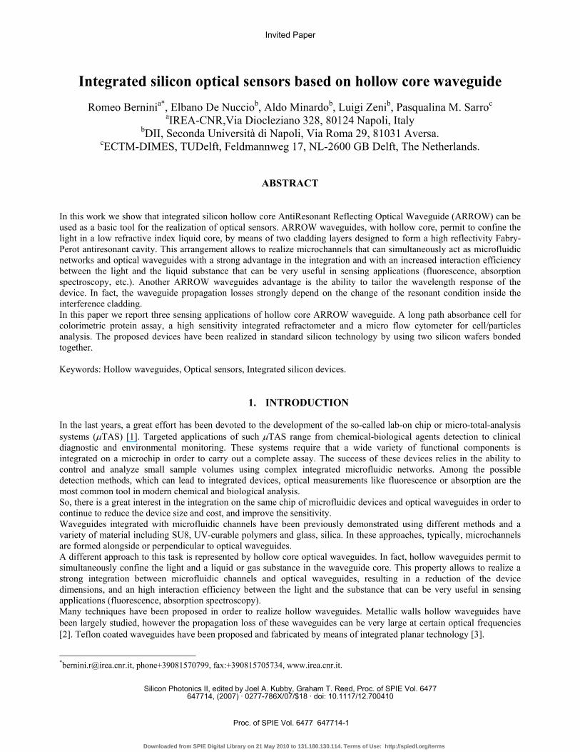
ARROW waveguides offer some particular properties due to their peculiar design. In particular, the interference phenomena in the Fabry-Perot cladding system permits to simply change the optical response of the waveguide as a function of both the geometrical parameters (dc, d1, d2) and the optical parameters (λ, nc, n1, n2). As an example, in Fig. 2 the attenuation of the TE fundamental mode is plotted as a function of the thickness d1 of the first cladding when dc=50µm and d2 is at its optimum. The working wavelength is λ=670nm, nc=1, n1=2.01 and n2=1.488.
0 0.1 0.2 0.3 0.4 0.510-3
10-2
10-1
100
d1 [µm]
α[c
m-1
]
λ=0.670µmλ=0.780µm
0 0.1 0.2 0.3 0.4 0.510-3
10-2
10-1
100
d1 [µm]
α[c
m-1
]
λ=0.670µmλ=0.780µm
Fig. 2. Attenuation of the ARROW fundamental TE mode as a function of the first cladding thickness d1 for λ=670nm (solid line) and λ=780nm (dashed line). dc=50µm and d2=0.1520µm.
As we can see from this figure, when the thickness d1 increases the attenuation goes through minima and maxima related to the antiresonance and resonance condition of the first cladding layer, as in typical Airy reflectivity fringe pattern. The minima are given by eq.(1) whereas the attenuation peaks are determined by the resonant condition that occurs approximately at:
[ ] ( )....,1,0MMnn2
d 21
2eff
21r1 =−
λ=
− (3)
Proc. of SPIE Vol. 6477 647714-3
Downloaded from SPIE Digital Library on 21 May 2010 to 131.180.130.114. Terms of Use: http://spiedl.org/terms

Similar considerations can be made for the second cladding. Another ARROW waveguides advantage is the ability to tailor the wavelength response of the device. As an example, in Fig. 2 is also reported the attenuation of the TE fundamental mode for λ=780nm, as a function of the thickness d1 of the first cladding when dc=50µm. The second cladding is designed to be antiresonant at λ=670nm. This shows that the spectral properties of the ARROW waveguide can be tuned with a suitable choice of the cladding layers thicknesses. In general, the propagation loss of the fundamental mode exhibits wavelength dependence from the change of the resonant condition inside the interference cladding. In fact, at resonance, the Fabry-Perot cavity exhibits a low reflectivity and the field penetrates into the high index substrate, leading to a strong increase of the radiation losses. In particular, the spectral response of an ARROW waveguide strongly depends on the refractive index of the core. In Fig. 3 the attenuation of the ARROW fundamental TE mode as a function of the wavelength λ, for different refractive indexes of the core, is depicted for λ=670nm, dc=50µm, d1=0.3334µm and d2=0.2510 µm.
0.4 0.5 0.6 0.7 0.810-4
10-3
10-2
10-1
100
λ [µm]
α[c
m-1
]
nc=1
nc =1.33nc =1.45
0.4 0.5 0.6 0.7 0.810-4
10-3
10-2
10-1
100
λ [µm]
α[c
m-1
]
nc=1
nc =1.33nc =1.45
Fig. 3. Attenuation of the ARROW fundamental TE mode as a function of the wavelength λ for different
refractive indexes of the core nc=1 (solid line), nc=1.33 (dashed line), nc=1.45 (dotted line) λ=670nm.
2.2. 2-D Integrated Hollow ARROW fabrication
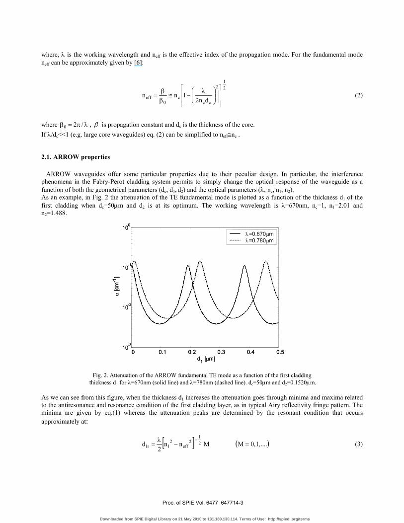
In order to realize an integrated hollow core ARROW waveguide it is necessary to obtain an ARROW confinement both in vertical and in lateral directions. Several geometries have been proposed that provide 2-D ARROW [8-12]. However, in the choice of the geometry one must take into account not only the optical properties, but also the available fabrication process. In fact, some geometries can require complex fabrication processes with small fabrication tolerances or poor optical quality. With respect to other proposed structures, the square cross section has been preferred in order to keep the technological efforts as low as possible. In fact, using standard bulk micromachining techniques it is possible to obtain good channels and avoid the need of aligned wafer bonding. In Fig. 4 a cross section of a 2-D hollow ARROW waveguide is reported.
Several hollow waveguides have been fabricated using silicon technology. The fabrication process starts with the realization of deep trench by silicon dry etching in the bottom wafer. The trench depth ranges from130µm to 150µm and the width ranges from 40µm to 250µm. Then, the cladding structure is formed by a PECVD or LPCVD deposition of silicon dioxide and silicon nitride on both wafers. After the deposition, the two halves were joined by silicon nitride direct wafer bonding or by glue.
Proc. of SPIE Vol. 6477 647714-4
Downloaded from SPIE Digital Library on 21 May 2010 to 131.180.130.114. Terms of Use: http://spiedl.org/terms
s u b s t r a ten 2 , d 2
n 1 , d 1
n 1 , d 1n 2 , d 2
s u b s tr a te
d c
Top wafer
Bottom wafer
Fig.4 Transverse section of the hollow core ARROW waveguide.
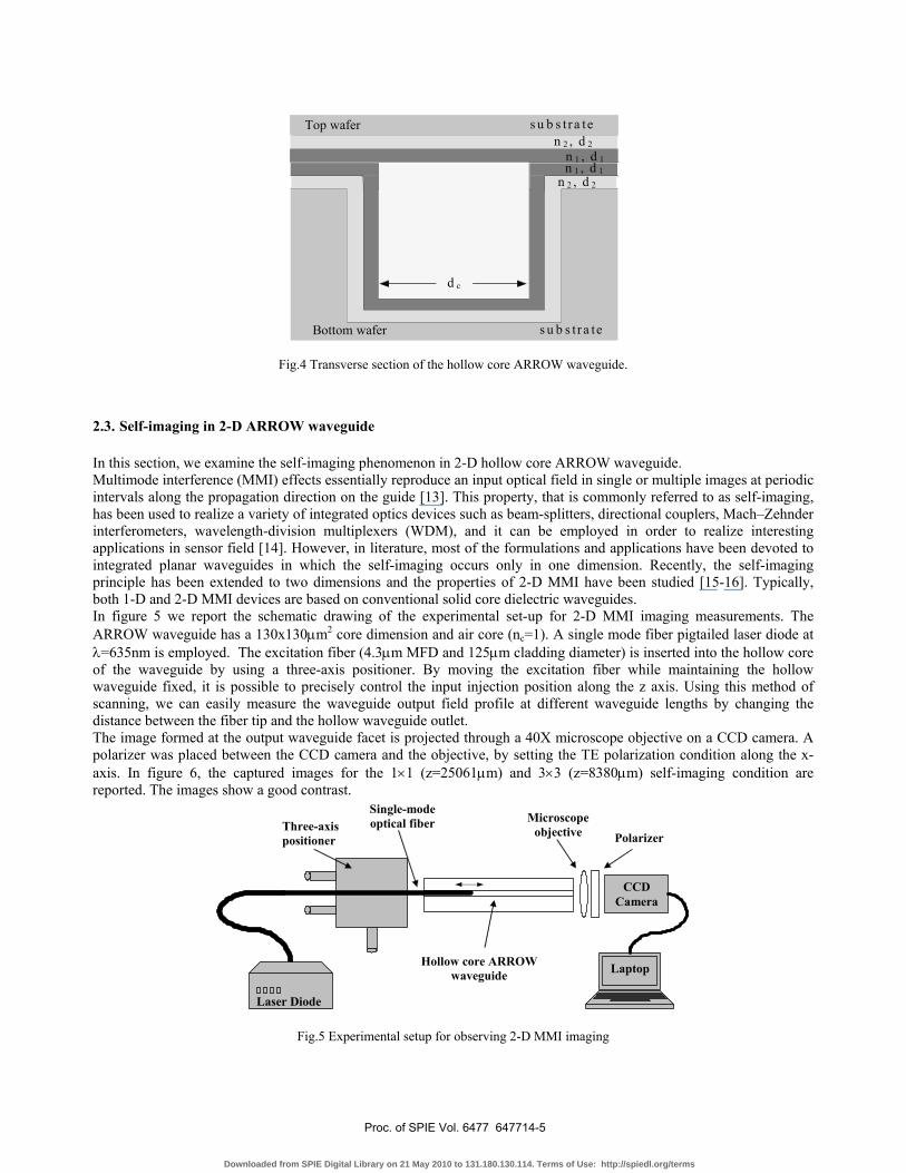
2.3. Self-imaging in 2-D ARROW waveguide In this section, we examine the self-imaging phenomenon in 2-D hollow core ARROW waveguide. Multimode interference (MMI) effects essentially reproduce an input optical field in single or multiple images at periodic intervals along the propagation direction on the guide [13]. This property, that is commonly referred to as self-imaging, has been used to realize a variety of integrated optics devices such as beam-splitters, directional couplers, Mach–Zehnder interferometers, wavelength-division multiplexers (WDM), and it can be employed in order to realize interesting applications in sensor field [14]. However, in literature, most of the formulations and applications have been devoted to integrated planar waveguides in which the self-imaging occurs only in one dimension. Recently, the self-imaging principle has been extended to two dimensions and the properties of 2-D MMI have been studied [15-16]. Typically, both 1-D and 2-D MMI devices are based on conventional solid core dielectric waveguides. In figure 5 we report the schematic drawing of the experimental set-up for 2-D MMI imaging measurements. The ARROW waveguide has a 130x130µm2 core dimension and air core (nc=1). A single mode fiber pigtailed laser diode at λ=635nm is employed. The excitation fiber (4.3µm MFD and 125µm cladding diameter) is inserted into the hollow core of the waveguide by using a three-axis positioner. By moving the excitation fiber while maintaining the hollow waveguide fixed, it is possible to precisely control the input injection position along the z axis. Using this method of scanning, we can easily measure the waveguide output field profile at different waveguide lengths by changing the distance between the fiber tip and the hollow waveguide outlet. The image formed at the output waveguide facet is projected through a 40X microscope objective on a CCD camera. A polarizer was placed between the CCD camera and the objective, by setting the TE polarization condition along the x-axis. In figure 6, the captured images for the 1×1 (z=25061µm) and 3×3 (z=8380µm) self-imaging condition are reported. The images show a good contrast.
CCD Camera
Laptop Hollow core ARROW waveguide
Microscope objective Three-axis
positioner
Single-mode optical fiber
Laser Diode
Polarizer
Fig.5 Experimental setup for observing 2-D MMI imaging
Proc. of SPIE Vol. 6477 647714-5
Downloaded from SPIE Digital Library on 21 May 2010 to 131.180.130.114. Terms of Use: http://spiedl.org/terms

Wx
Wy
0 20 40 60 80 100 1200
20
40
60
80
100
120
Wx
Wy
0 20 40 60 80 100 1200
20
40
60
80
100
120
Fig. 6 CCD captured output intensity distribution with image matrix 1×1; 3×3 .
An interesting property of the MMI device is its spectral filtering capability. In order to investigate this effect in 2-D ARROW waveguides, the experimental set-up shown in Figure 5 is slightly modified by replacing the laser diode with a white light lamp. Moreover a single mode fiber, identical to the input one, is inserted into the waveguide output in order to collect and deliver the output radiation to a CCD spectrometer. The transmitted spectra are measured by changing the distance Lf between the two fiber tips. In figure 7 the normalized transmitted spectrum for Lf =23300µm, is reported. The device exhibits a narrow bandpass spectral behavior that can be easily explained taking into account the self-imaging principle. In fact the transmitted intensity at a fixed wavelength, depends on the overlap between the field of the multimode ARROW waveguide at z=Lf and the modal field of the collecting single mode fiber. The maximum overlap is reached at the wavelength for which a single image of the input field is obtained. The full-width-half-maximum (FWHM) bandwidth is about 10nm. By increasing the distance Lf between the fibers, the peak of the transmitted spectrum shifts toward lower wavelengths, verifying the single imaging condition. This filtering property can be usefully applied in sensing applications for spectral analysis and fluorescence detection.
600 650 700 750 800 850 9000
0.2
0.4
0.6
0.8
1
Wavelength [nm]
Nor
mal
ized
tran
smitt
ed in
tens
ity
Fig. 7 Normalized transmitted spectrum for Lf =23300µm.
Proc. of SPIE Vol. 6477 647714-6
Downloaded from SPIE Digital Library on 21 May 2010 to 131.180.130.114. Terms of Use: http://spiedl.org/terms
3. SENSORS BASED ON HOLLOW CORE WAVEGUIDE In this section, we report three sensing applications of hollow core ARROW waveguide. A long path absorbance cell for colorimetric protein assay, a high sensitivity integrated refractometer and a micro flow cytometer for cell/particles analysis.
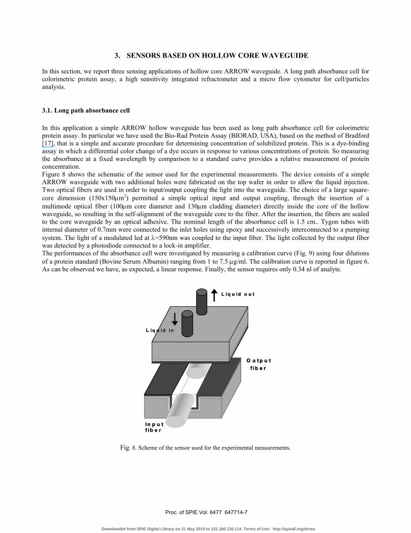
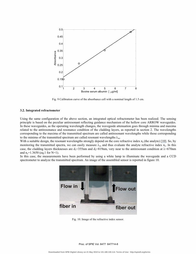
3.1. Long path absorbance cell In this application a simple ARROW hollow waveguide has been used as long path absorbance cell for colorimetric protein assay. In particular we have used the Bio-Rad Protein Assay (BIORAD, USA), based on the method of Bradford [17], that is a simple and accurate procedure for determining concentration of solubilized protein. This is a dye-binding assay in which a differential color change of a dye occurs in response to various concentrations of protein. So measuring the absorbance at a fixed wavelength by comparison to a standard curve provides a relative measurement of protein concentration. Figure 8 shows the schematic of the sensor used for the experimental measurements. The device consists of a simple ARROW waveguide with two additional holes were fabricated on the top wafer in order to allow the liquid injection. Two optical fibers are used in order to input/output coupling the light into the waveguide. The choice of a large square-core dimension (150x150µm2) permitted a simple optical input and output coupling, through the insertion of a multimode optical fiber (100µm core diameter and 130µm cladding diameter) directly inside the core of the hollow waveguide, so resulting in the self-alignment of the waveguide core to the fiber. After the insertion, the fibers are sealed to the core waveguide by an optical adhesive. The nominal length of the absorbance cell is 1.5 cm.. Tygon tubes with internal diameter of 0.7mm were connected to the inlet holes using epoxy and successively interconnected to a pumping system. The light of a modulated led at λ=590nm was coupled to the input fiber. The light collected by the output fiber was detected by a photodiode connected to a lock-in amplifier. The performances of the absorbance cell were investigated by measuring a calibration curve (Fig. 9) using four dilutions of a protein standard (Bovine Serum Albumin) ranging from 1 to 7.5 µg/ml. The calibration curve is reported in figure 6. As can be observed we have, as expected, a linear response. Finally, the sensor requires only 0.34 nl of analyte.
I n p u tf ib e r
O u t p u tf i b e r
L iq u id in
L iq u id o u t
I n p u tf ib e r
O u t p u tf i b e r
L iq u id in
L iq u id o u t
Fig. 8. Scheme of the sensor used for the experimental measurements.
Proc. of SPIE Vol. 6477 647714-7
Downloaded from SPIE Digital Library on 21 May 2010 to 131.180.130.114. Terms of Use: http://spiedl.org/terms
1 2 3 4 5 6 7 80.1
0.15
0.2
0.25
0.3
0.35
0.4
0.45
0.5
Bovine serum albumin [ µg/ml]
Abs
orba
nce
Fig. 9 Calibration curve of the absorbance cell with a nominal length of 1.5 cm.
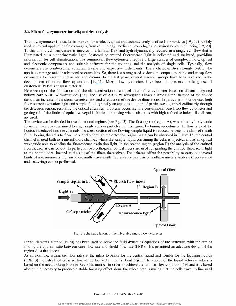
3.2. Integrated refractometer Using the same configuration of the above section, an integrated optical refractometer has been realized. The sensing principle is based on the peculiar antiresonant reflecting guidance mechanism of the hollow core ARROW waveguides. In these waveguides, as the operating wavelength changes, the waveguide attenuation goes through minima and maxima related to the antiresonance and resonance condition of the cladding layers, as reported in section 2. The wavelengths corresponding to the maxima of the transmitted spectrum are called antiresonant wavelengths while those corresponding to the minima of the transmitted spectrum are called resonant wavelengths λm. With a suitable design, the resonant wavelengths strongly depend on the core refractive index nc (the analyte) [10]. So, by monitoring the transmitted spectra, we can easily measure λm and thus evaluate the analyte refractive index nc. In this case, the cladding layers thicknesses are d1=355nm and d2=819nm, very near to the antiresonant condition at λ=670nm and nc=1.3650 (eq.1 for N=1). In this case, the measurements have been performed by using a white lamp to illuminate the waveguide and a CCD spectrometer to analyze the transmitted spectrum. An image of the assembled sensor is reported in figure 10.
fiber in fiber out
Flow in Flow out
Fig. 10. Image of the refractive index sensor.
Proc. of SPIE Vol. 6477 647714-8
Downloaded from SPIE Digital Library on 21 May 2010 to 131.180.130.114. Terms of Use: http://spiedl.org/terms

A series of measurements with different liquid mixtures, whose refractive indices range from 1.3400 to 1.4459, has been performed with a sensing length of 1cm. The wavelength λm strongly shifts toward the lower wavelengths, as the core refractive index increases. In Fig.11, the normalized transmittance is reported as a function of the wavelength for different refractive index values. The experimental wavelength shift of the resonance as a function of the core refractive index nc is depicted in Fig. 12, together with the model data [18]. The proposed sensor exhibits a slightly non linear response over a wide refractive index range and a sensitivity cm nS ∂λ∂= that ranges from S=1500nm (nc=1.3330) to S=5000nm (nc=1.4450). This corresponds, assuming a spectral resolution of 10pm, to a detectable refractive index change as small as 2⋅10-6.
600 650 700 750 800 8500.95
1
1.05
1.1
1.15
1.2
1.25
Nor
mal
ized
tran
smitt
ed in
tens
ity [a
.u]
wavelength [nm]
nc
Fig. 11. Normalized transmittance as a function of the wavelength for different refractive index values.
500 600 700 800 900 10001.32
1.34
1.36
1.38
1.4
1.42
1.44
1.46
Cor
e re
fract
ive
inde
x n c
Resonant wavelength λm[nm]
Experimetal resultsSimulation
Fig. 12. Sensor response: Simulation and experimental results.
Proc. of SPIE Vol. 6477 647714-9
Downloaded from SPIE Digital Library on 21 May 2010 to 131.180.130.114. Terms of Use: http://spiedl.org/terms
Sample liquid hilet
Light h
Sheath flow inlets
Opticalfiber
Cells/pa 'tides Fk,orecence light
Opticalfiber
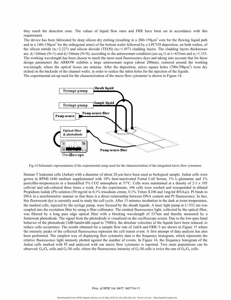
3.3. Micro flow cytometer for cell/particles analysis. The flow cytometer is a useful instrument for a selective, fast and accurate analysis of cells or particles [19]. It is widely used in several application fields ranging from cell biology, medicine, toxicology and environmental monitoring [19, 20]. To this aim, a cell suspension is injected in a laminar flow and hydrodynamically focused in a single cell flow that is illuminated by a monochromatic light. Scattered or emitted fluorescence light is collected and analyzed, providing information for cell classification. The commercial flow cytometers require a large number of complex fluidic, optical and electronic components and suitable software for the counting and the analysis of single cells. Typically, flow cytometers are cumbersome, complex, fragile and expensive instruments. These characteristics strongly restrict the application range outside advanced research labs. So, there is a strong need to develop compact, portable and cheap flow cytometers for research and in situ applications. In the last years, several research groups have been involved in the development of micro flow cytometers [19-24]. Micro flow cytometers have been demonstrated making use of elastomers (PDMS) or glass materials. Here we report the fabrication and the characterization of a novel micro flow cytometer based on silicon integrated hollow core ARROW waveguides [25]. The use of ARROW waveguide allows a strong simplification of the device design, an increase of the signal-to-noise ratio and a reduction of the device dimensions. In particular, in our devices both fluorescence excitation light and sample fluid, typically an aqueous solution of particles/cells, travel collinearly through the detection region, resolving the optical alignment problems occurring in a conventional bench top flow cytometer and getting rid of the limits of optical waveguide fabrication arising when substrates with high refractive index, like silicon, are used. The device can be divided in two functional regions (see Fig.13). The first region (region A), where the hydrodynamic focusing takes place, is aimed to align single cells or particles. In this region, by tuning opportunely the flow rates of the liquids introduced into the channels, the cross section of the flowing sample liquid is reduced between the slabs of sheath fluid, forcing the cells to flow individually through the detection region. As it can be observed in Figure 13, the central channel is used both as a microfluidic channel, where the sample liquid containing the cells is injected, and as an optical waveguide able to confine the fluorescence excitation light. In the second region (region B) the analysis of the emitted fluorescence is carried out. In particular, two orthogonal optical fibers are used for guiding the emitted fluorescent light to the photodiodes, located at the exit of the fibers themselves. The scheme offers the possibility to carry out several kinds of measurements. For instance, multi wavelength fluorescence analysis or multiparameters analysis (fluorescence and scattering) can be performed.
Fig.13 Schematic layout of the integrated micro flow cytometer
Finite Elements Method (FEM) has been used to solve the fluid dynamics equations of the structure, with the aim of finding the optimal ratio between core flow rate and shield flow rate (FRR). This permitted an adequate design of the region A of the device. As an example, setting the flow rates at the inlets to 5ml/h for the central liquid and 15ml/h for the focusing liquids (FRR=3) the calculated cross section of the focused stream is about 20µm. The choice of the liquid velocity values is based on the need to keep low the Reynolds number in order to achieve the laminar flow condition [19] and it is based also on the necessity to produce a stable focusing effect along the whole path, assuring that the cells travel in line until
Region A
Region B
Proc. of SPIE Vol. 6477 647714-10
Downloaded from SPIE Digital Library on 21 May 2010 to 131.180.130.114. Terms of Use: http://spiedl.org/terms
Sathd
U S nib ScOpe
Pump solute fiber
they reach the detection zone. The values of liquid flow rates and FRR have been set in accordance with this requirement. The device has been fabricated by deep silicon dry etching (resulting in a 200×150µm2 core for the flowing liquid path and in a 140×150µm2 for the orthogonal arms) of the bottom wafer followed by a LPCVD deposition, on both wafers, of the silicon nitride (n1=2.227) and silicon dioxide (TEOS) (n2=1.457) cladding layers. The cladding layers thicknesses are: d1=266nm (N=1) and d2=266nm (N=0), according to the antiresonant condition (see eq.1) at λ=633nm and nc=1.333. The working wavelength has been chosen to mach the most used fluorescence dyes and taking into account that for these design parameters the ARROW exhibits a large antiresonant region (about 200nm), centered around the working wavelength, where the optical losses are minima. After the deposition, micro square holes (700x700µm2) were dry etched on the backside of the channel wafer, in order to realize the inlets holes for the injection of the liquids. The experimental set-up used for the characterization of the micro flow cytometer is shown in Figure 14.
Optical filter & photodiode
Fig.14 Schematic representation of the experimental setup used for the characterization of the integrated micro flow cytometer.
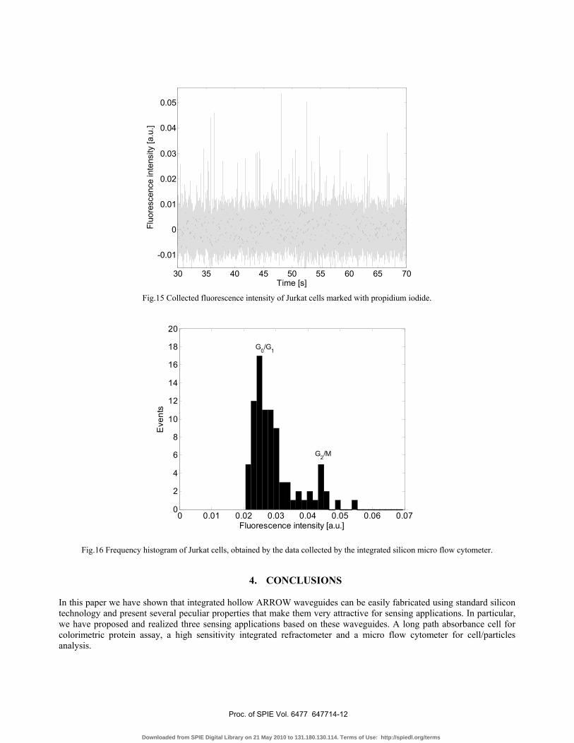
Human T leukemia cells (Jurkat) with a diameter of about 20 µm have been used as biological sample. Jurkat cells were grown in RPMI-1640 medium supplemented with 10% heat-inactivated Foetal Calf Serum, 1% L-glutamine and 1% penicillin-streptomycin in a humidified 5% CO2 atmosphere at 37°C. Cells were maintained at a density of 2-3 x 10⁵ cells/ml and sub-cultured three times a week. For the experiments, 106 cells were washed and resuspended in diluted Propidium Iodide (PI) solution (50 mg/ml in 0.1% trisodium citrate, 0.1% Triton X100 and 1mg/ml RNAse). PI binds to DNA in a stoichiometric manner so that there is a direct relationship between DNA content and PI fluorescence. In fact, this fluorescent dye is currently used to study the cell cycle. After 15 minutes incubation in the dark at room temperature, the marked cells, injected by the syringe pump, were focused by the sheath liquids. A laser light pump at λ=532 nm was coupled into the excitation fiber by using a fiber collimator. The emitted fluorescence light, collected by the optical fiber, was filtered by a long pass edge optical filter with a blocking wavelength of 537nm and thereby measured by a femtowatt photodiode. The signal from the photodiode is visualized on the oscilloscope screen. Due to the low-pass band behavior of the photodiode (3dB bandwidth equal to 750Hz), the absolute velocities of the liquids have been reduced, to reduce cells occurrence. The results obtained for a sample flow rate of 1ml/h and FRR=3 are shown in Figure 15 where the intensity peaks of the collected fluorescence represent the cell transit event. A first attempt of data analysis has also been performed. The simplest way of displaying flow cytometry data is the frequency histogram, which represents the relative fluorescence light intensity plotted against the number of events. In Figure 16, the frequency histogram of the Jurkat cells marked with PI and analyzed with our micro flow cytometer is reported. Two main populations can be observed: G0/G1 cells and G2/M cells, where the fluorescence intensity of G2/M cells is twice the one of G0/G1 cells.
Proc. of SPIE Vol. 6477 647714-11
Downloaded from SPIE Digital Library on 21 May 2010 to 131.180.130.114. Terms of Use: http://spiedl.org/terms
30 35 40 45 50 55 60 65 70
-0.01
0
0.01
0.02
0.03
0.04
0.05
Time [s]
Fluo
resc
ence
inte
nsity
[a.u
.]
Fig.15 Collected fluorescence intensity of Jurkat cells marked with propidium iodide.
0 0.01 0.02 0.03 0.04 0.05 0.06 0.070
2
4
6
8
10
12
14
16
18
20
Fluorescence intensity [a.u.]
Eve
nts
G0/G1
G2/M
Fig.16 Frequency histogram of Jurkat cells, obtained by the data collected by the integrated silicon micro flow cytometer.
4. CONCLUSIONS In this paper we have shown that integrated hollow ARROW waveguides can be easily fabricated using standard silicon technology and present several peculiar properties that make them very attractive for sensing applications. In particular, we have proposed and realized three sensing applications based on these waveguides. A long path absorbance cell for colorimetric protein assay, a high sensitivity integrated refractometer and a micro flow cytometer for cell/particles analysis.
Proc. of SPIE Vol. 6477 647714-12
Downloaded from SPIE Digital Library on 21 May 2010 to 131.180.130.114. Terms of Use: http://spiedl.org/terms

ACKNOWLEDGEMENTS The authors would like to thank the IC Process Group of DIMES for technical assistance in the device fabrication and F.Brescia, R.Palumbo and M.R.Scarfi for their assistance in the preparation of the biological samples.
REFERENCES 1. A. Manz, N. Graber, M. Widmer, “Miniaturized total chemical analysis systems: a novel concept for chemical
sensing”, Sens. Actuators B 1, 244–248, (1990). 2. J. N. McMullin, R. Narendra and C:R. James, “Hollow metallic waveguides in Silicon V-grooves”, IEEE Photon.
Technol. Lett. 5, 1080-1082, (1993). 3. A. Datta,; E. In-Yong; A. Dhar, P. Kuban, R. Manor, I. Ahmad, S. Gangopadhyay, T. Dallas, M. Holtz, H. Temkin,
P.K. Dasgupta, “Microfabrication and characterization of teflon AF-coated liquid core waveguide channels in silicon”, IEEE Sens. Journal 3, 788 – 795, (2003).
4. S.S. Lo, M.S.Wang, C.C. Chen, “Semiconductor hollow optical waveguides formed by omni-directional reflectors“, Optics Express 12, 6589-6593, (2004).
5. A. Grosse, M. Grewe and H. Fouckhardt, “Deep wet etching of fused silica glass for hollow capillary optical leaky waveguides in microfluidic devices”, J. Micromech. Microeng. 11, 257-262, (2001).
6. T. Baba and Y. Kokubun, “Dispersion and radiation loss characteristics of antiresonant reflecting optical waveguides – numerical results and analytical expressions”, IEEE J. Quantum. Electron. 28, 1689-1700, (1992).
7. N.J. Goddard, K. Singh, F. Bounaria, R.J. Holmes, S.J. Baldock, L.W. Pickering, P.R. Fielden and R.D. Snook, “Anti-Resonant Reflecting Optical Waveguides (ARROWS) as Optimal Optical Detectors for MicroTAS Applications”, in Proceedings of the µTAS ’98 Workshop, D.J. Harrison and A. Van Den Berg, ed. Kluwer , 97, (1998).
8. T. Delonges and H. Fouckhardt, “Integrated optical detection cell based on Bragg reflecting waveguides”, J. of Chromatography A 716, 135-139, (1995).
9. R. Bernini, S. Campopiano, L. Zeni, “Silicon Micromachined Hollow Optical Waveguides for Sensing Applications”, IEEE J. Selected Topics in Quantum Elect. 8, 106, (2002).
10. S. Campopiano, R. Bernini, L. Zeni, P.M. Sarro, “Microfluidic sensor based on integrated optical hollow waveguide”, Optics Lett. 29, 1894-1896, (2004).
11. D.Yin, D.W Deamer, H.Schmidt, J.P. Barber, A.R.Hawkins, “Integrated optical waveguides with liquid cores”, Appl. Phys. Lett. 85, 3477-3479, (2004).
12. D. Yin, H. Schmidt, J. P. Barber, E. J. Lunt, A. R. Hawkins, “Optical characterization of arch-shaped ARROW waveguides with liquid cores Optics Express 13, 10564 - 10570, (2005).
13. L. Soldano and E. Pennings, “Optical multi-mode interference devices based on self-imaging: Principles and applications,” J. Lightw. Technol. 13, 615–627, (1995).
14. K.R. Kribich , R. Copperwhite, H. Barry, B. Kolodziejczyk, J.-M. Sabatti´e, K. O’Dwyer, B.D. MacCraith, “Novel chemical sensor/biosensor platform based on optical multimode interference (MMI) couplers”, Sensors and Actuators B 107, 188–192, (2005).
15. D. Khalil and A. Yehia, “Two-dimensional multimode interference in integrated optical structures,” J. Opt. A, Pure Appl. Opt. 6, 137–145, (2004)..
16. H. Chen and D. T. K. Tong, “Two-dimensional symmetric multimode Interferences in Silicon Square Waveguides”, IEEE Photon. Technol. Lett.17, 801-803, (2005).
17. M.Bradford, "A Rapid and Sensitive Method for the Quantitation of Microgram Quantities of Protein Utilizing the Principle of Protein-Dye Binding" Anal. Biochem. 72, 248-254, (1976).
18. J.L. Archambault, R.J. Balck, S.Lacroix, J.Bures, “Loss calculations for antiresonant Waveguides”, J. Lightwave Technol. 11, 416-423, (1993).
19. D.Huh, W. Gu, Y. Kamotani, J. B. Groteberg, S. Takayama, “Microfluidics for flow cytometric analysis of cells and particles”, Physiol. Meas. 26, 73-98, (2005).
20. C. Grunde, S. Skerlos, P. Adriaens, “Flow cytometry for microbial sensing in environmental sustainability applications: current status and future prospescpects”, FEMS micorbiology ecology 49, 37-49, (2004).
Proc. of SPIE Vol. 6477 647714-13
Downloaded from SPIE Digital Library on 21 May 2010 to 131.180.130.114. Terms of Use: http://spiedl.org/terms
21. Y. C. Tung, M. Zhang, C. T. Lin, K. Kurabayashi, S.J. Skerlos, “PDMS-based opto-fluidic micro flow cytometer with two-color, multi-angle fluorescence detection capability using PIN photodiodes”, Sensors and Actuators B 98, 356-367, (2004).
22. C.H. Lin, G.B. Lee, “Micromachined flow cytometers with embedded etched optic fibers for optical detection”, J. Micromech. Microeng. 13, 447-453, (2003).
23. J. Kruger, K. Singh, A. O’Neill, C. Jackson, A. Morrison, P. O’Brien, “Development of a microfluidic device for fluorescence activated cell sorting”, J. Micromech. Microeng. 12, 486-494, (2002).
24. Z. Wang, J. El-Ali, M. Engelund, T. Gotsæd, I. R. Perch-Nielsen, K. B. Mogensen, D.Snakenborg, J. P. Kutter and A. Wolff, “Measurements of scattered light on a microchip flow cytometer with integrated polymer based optical elements”, Lab on chip 4, 372-377, (2004).
25. R. Bernini . E. De Nuccio,F. Brescia, A. Minardo, L. Zeni, P. M. Sarro, R. Palumbo, M. R. Scarfi, “Development and characterization of an integrated silicon micro flow cytometer”, Analytical and Bioanalytical Chemistry, 386, 1267–1272, (2006).
Proc. of SPIE Vol. 6477 647714-14
Downloaded from SPIE Digital Library on 21 May 2010 to 131.180.130.114. Terms of Use: http://spiedl.org/terms