
Sensors & Transducers
353
-
Upload
khangminh22 -
Category
Documents
-
view
0 -
download
0
Transcript of Sensors & Transducers


SSeennssoorrss && TTrraannssdduucceerrss
Special Issue April 2008
www.sensorsportal.com ISSN 1726-5479
Editor-in-Chief: Sergey Y. Yurish
Guest Editors: Subhas Chandra Mukhopadhyay and Gourab Sen Gupta
Editors for Western Europe Meijer, Gerard C.M., Delft University of Technology, The Netherlands Ferrari, Vittorio, UUnniivveerrssiittáá ddii BBrreesscciiaa,, IIttaaly Editors for North America Datskos, Panos G., OOaakk RRiiddggee NNaattiioonnaall LLaabboorraattoorryy,, UUSSAA Fabien, J. Josse, Marquette University, USA Katz, Evgeny, Clarkson University, USA
Editor South America Costa-Felix, Rodrigo, Inmetro, Brazil Editor for Eastern Europe Sachenko, Anatoly, Ternopil State Economic University, Ukraine Editor for Asia Ohyama, Shinji, Tokyo Institute of Technology, Japan
Editorial Advisory Board
Abdul Rahim, Ruzairi, Universiti Teknologi, Malaysia Ahmad, Mohd Noor, Nothern University of Engineering, Malaysia Annamalai, Karthigeyan, National Institute of Advanced Industrial Science and
Technology, Japan Arcega, Francisco, University of Zaragoza, Spain Arguel, Philippe, CNRS, France Ahn, Jae-Pyoung, Korea Institute of Science and Technology, Korea Arndt, Michael, Robert Bosch GmbH, Germany Ascoli, Giorgio, George Mason University, USA Atalay, Selcuk, Inonu University, Turkey Atghiaee, Ahmad, University of Tehran, Iran Augutis, Vygantas, Kaunas University of Technology, Lithuania Avachit, Patil Lalchand, North Maharashtra University, India Ayesh, Aladdin, De Montfort University, UK Bahreyni, Behraad, University of Manitoba, Canada Baoxian, Ye, Zhengzhou University, China Barford, Lee, Agilent Laboratories, USA Barlingay, Ravindra, RF Arrays Systems, India Basu, Sukumar, Jadavpur University, India Beck, Stephen, University of Sheffield, UK Ben Bouzid, Sihem, Institut National de Recherche Scientifique, Tunisia Binnie, T. David, Napier University, UK Bischoff, Gerlinde, Inst. Analytical Chemistry, Germany Bodas, Dhananjay, IMTEK, Germany Borges Carval, Nuno, Universidade de Aveiro, Portugal Bousbia-Salah, Mounir, University of Annaba, Algeria Bouvet, Marcel, CNRS – UPMC, France Brudzewski, Kazimierz, Warsaw University of Technology, Poland Cai, Chenxin, Nanjing Normal University, China Cai, Qingyun, Hunan University, China Campanella, Luigi, University La Sapienza, Italy Carvalho, Vitor, Minho University, Portugal Cecelja, Franjo, Brunel University, London, UK Cerda Belmonte, Judith, Imperial College London, UK Chakrabarty, Chandan Kumar, Universiti Tenaga Nasional, Malaysia Chakravorty, Dipankar, Association for the Cultivation of Science, India Changhai, Ru, Harbin Engineering University, China Chaudhari, Gajanan, Shri Shivaji Science College, India Chen, Jiming, Zhejiang University, China Chen, Rongshun, National Tsing Hua University, Taiwan Cheng, Kuo-Sheng, National Cheng Kung University, Taiwan Chiriac, Horia, National Institute of Research and Development, Romania Chowdhuri, Arijit, University of Delhi, India Chung, Wen-Yaw, Chung Yuan Christian University, Taiwan Corres, Jesus, Universidad Publica de Navarra, Spain Cortes, Camilo A., Universidad Nacional de Colombia, Colombia Courtois, Christian, Universite de Valenciennes, France Cusano, Andrea, University of Sannio, Italy D'Amico, Arnaldo, Università di Tor Vergata, Italy De Stefano, Luca, Institute for Microelectronics and Microsystem, Italy Deshmukh, Kiran, Shri Shivaji Mahavidyalaya, Barshi, India Kang, Moonho, Sunmoon University, Korea South Kaniusas, Eugenijus, Vienna University of Technology, Austria Katake, Anup, Texas A&M University, USA Kausel, Wilfried, University of Music, Vienna, Austria
Dickert, Franz L., Vienna University, Austria Dieguez, Angel, University of Barcelona, Spain Dimitropoulos, Panos, University of Thessaly, Greece Ding Jian, Ning, Jiangsu University, China Djordjevich, Alexandar, City University of Hong Kong, Hong Kong Donato, Nicola, University of Messina, Italy Donato, Patricio, Universidad de Mar del Plata, Argentina Dong, Feng, Tianjin University, China Drljaca, Predrag, Instersema Sensoric SA, Switzerland Dubey, Venketesh, Bournemouth University, UK Enderle, Stefan, University of Ulm and KTB Mechatronics GmbH, Germany Erdem, Gursan K. Arzum, Ege University, Turkey Erkmen, Aydan M., Middle East Technical University, Turkey Estelle, Patrice, Insa Rennes, France Estrada, Horacio, University of North Carolina, USA Faiz, Adil, INSA Lyon, France Fericean, Sorin, Balluff GmbH, Germany Fernandes, Joana M., University of Porto, Portugal Francioso, Luca, CNR-IMM Institute for Microelectronics and Microsystems,
Italy Francis, Laurent, University Catholique de Louvain, Belgium Fu, Weiling, South-Western Hospital, Chongqing, China Gaura, Elena, Coventry University, UK Geng, Yanfeng, China University of Petroleum, China Gole, James, Georgia Institute of Technology, USA Gong, Hao, National University of Singapore, Singapore Gonzalez de la Rosa, Juan Jose, University of Cadiz, Spain Granel, Annette, Goteborg University, Sweden Graff, Mason, The University of Texas at Arlington, USA Guan, Shan, Eastman Kodak, USA Guillet, Bruno, University of Caen, France Guo, Zhen, New Jersey Institute of Technology, USA Gupta, Narendra Kumar, Napier University, UK Hadjiloucas, Sillas, The University of Reading, UK Hashsham, Syed, Michigan State University, USA Hernandez, Alvaro, University of Alcala, Spain Hernandez, Wilmar, Universidad Politecnica de Madrid, Spain Homentcovschi, Dorel, SUNY Binghamton, USA Horstman, Tom, U.S. Automation Group, LLC, USA Hsiai, Tzung (John), University of Southern California, USA Huang, Jeng-Sheng, Chung Yuan Christian University, Taiwan Huang, Star, National Tsing Hua University, Taiwan Huang, Wei, PSG Design Center, USA Hui, David, University of New Orleans, USA Jaffrezic-Renault, Nicole, Ecole Centrale de Lyon, France Jaime Calvo-Galleg, Jaime, Universidad de Salamanca, Spain James, Daniel, Griffith University, Australia Janting, Jakob, DELTA Danish Electronics, Denmark Jiang, Liudi, University of Southampton, UK Jiao, Zheng, Shanghai University, China John, Joachim, IMEC, Belgium Kalach, Andrew, Voronezh Institute of Ministry of Interior, Russia Rodriguez, Angel, Universidad Politecnica de Cataluna, Spain Rothberg, Steve, Loughborough University, UK Sadana, Ajit, University of Mississippi, USA

Kavasoglu, Nese, Mugla University, Turkey Ke, Cathy, Tyndall National Institute, Ireland Khan, Asif, Aligarh Muslim University, Aligarh, India Kim, Min Young, Koh Young Technology, Inc., Korea South Ko, Sang Choon, Electronics and Telecommunications Research Institute, Korea
South Kockar, Hakan, Balikesir University, Turkey Kotulska, Malgorzata, Wroclaw University of Technology, Poland Kratz, Henrik, Uppsala University, Sweden Kumar, Arun, University of South Florida, USA Kumar, Subodh, National Physical Laboratory, India Kung, Chih-Hsien, Chang-Jung Christian University, Taiwan Lacnjevac, Caslav, University of Belgrade, Serbia Lay-Ekuakille, Aime, University of Lecce, Italy Lee, Jang Myung, Pusan National University, Korea South Lee, Jun Su, Amkor Technology, Inc. South Korea Lei, Hua, National Starch and Chemical Company, USA Li, Genxi, Nanjing University, China Li, Hui, Shanghai Jiaotong University, China Li, Xian-Fang, Central South University, China Liang, Yuanchang, University of Washington, USA Liawruangrath, Saisunee, Chiang Mai University, Thailand Liew, Kim Meow, City University of Hong Kong, Hong Kong Lin, Hermann, National Kaohsiung University, Taiwan Lin, Paul, Cleveland State University, USA Linderholm, Pontus, EPFL - Microsystems Laboratory, Switzerland Liu, Aihua, University of Oklahoma, USA Liu Changgeng, Louisiana State University, USA Liu, Cheng-Hsien, National Tsing Hua University, Taiwan Liu, Songqin, Southeast University, China Lodeiro, Carlos, Universidade NOVA de Lisboa, Portugal Lorenzo, Maria Encarnacio, Universidad Autonoma de Madrid, Spain Lukaszewicz, Jerzy Pawel, Nicholas Copernicus University, Poland Ma, Zhanfang, Northeast Normal University, China Majstorovic, Vidosav, University of Belgrade, Serbia Marquez, Alfredo, Centro de Investigacion en Materiales Avanzados, Mexico Matay, Ladislav, Slovak Academy of Sciences, Slovakia Mathur, Prafull, National Physical Laboratory, India Maurya, D.K., Institute of Materials Research and Engineering, Singapore Mekid, Samir, University of Manchester, UK Melnyk, Ivan, Photon Control Inc., Canada Mendes, Paulo, University of Minho, Portugal Mennell, Julie, Northumbria University, UK Mi, Bin, Boston Scientific Corporation, USA Minas, Graca, University of Minho, Portugal Moghavvemi, Mahmoud, University of Malaya, Malaysia Mohammadi, Mohammad-Reza, University of Cambridge, UK Molina Flores, Esteban, Benemérita Universidad Autónoma de Puebla, Mexico Moradi, Majid, University of Kerman, Iran Morello, Rosario, DIMET, University "Mediterranea" of Reggio Calabria, Italy Mounir, Ben Ali, University of Sousse, Tunisia Mukhopadhyay, Subhas, Massey University, New Zealand Neelamegam, Periasamy, Sastra Deemed University, India Neshkova, Milka, Bulgarian Academy of Sciences, Bulgaria Oberhammer, Joachim, Royal Institute of Technology, Sweden Ould Lahoucin, University of Guelma, Algeria Pamidighanta, Sayanu, Bharat Electronics Limited (BEL), India Pan, Jisheng, Institute of Materials Research & Engineering, Singapore Park, Joon-Shik, Korea Electronics Technology Institute, Korea South Penza, Michele, ENEA C.R., Italy Pereira, Jose Miguel, Instituto Politecnico de Setebal, Portugal Petsev, Dimiter, University of New Mexico, USA Pogacnik, Lea, University of Ljubljana, Slovenia Post, Michael, National Research Council, Canada Prance, Robert, University of Sussex, UK Prasad, Ambika, Gulbarga University, India Prateepasen, Asa, Kingmoungut's University of Technology, Thailand Pullini, Daniele, Centro Ricerche FIAT, Italy Pumera, Martin, National Institute for Materials Science, Japan Radhakrishnan, S. National Chemical Laboratory, Pune, India Rajanna, K., Indian Institute of Science, India Ramadan, Qasem, Institute of Microelectronics, Singapore Rao, Basuthkar, Tata Inst. of Fundamental Research, India Raoof, Kosai, Joseph Fourier University of Grenoble, France Reig, Candid, University of Valencia, Spain Restivo, Maria Teresa, University of Porto, Portugal Robert, Michel, University Henri Poincare, France Rezazadeh, Ghader, Urmia University, Iran Royo, Santiago, Universitat Politecnica de Catalunya, Spain
Sadeghian Marnani, Hamed, TU Delft, The Netherlands Sandacci, Serghei, Sensor Technology Ltd., UK Sapozhnikova, Ksenia, D.I.Mendeleyev Institute for Metrology, Russia Saxena, Vibha, Bhbha Atomic Research Centre, Mumbai, India Schneider, John K., Ultra-Scan Corporation, USA Seif, Selemani, Alabama A & M University, USA Seifter, Achim, Los Alamos National Laboratory, USA Sengupta, Deepak, Advance Bio-Photonics, India Shearwood, Christopher, Nanyang Technological University, Singapore Shin, Kyuho, Samsung Advanced Institute of Technology, Korea Shmaliy, Yuriy, Kharkiv National University of Radio Electronics, Ukraine Silva Girao, Pedro, Technical University of Lisbon, Portugal Singh, V. R., National Physical Laboratory, India Slomovitz, Daniel, UTE, Uruguay Smith, Martin, Open University, UK Soleymanpour, Ahmad, Damghan Basic Science University, Iran Somani, Prakash R., Centre for Materials for Electronics Technol., India Srinivas, Talabattula, Indian Institute of Science, Bangalore, India Srivastava, Arvind K., Northwestern University, USA Stefan-van Staden, Raluca-Ioana, University of Pretoria, South Africa Sumriddetchka, Sarun, National Electronics and Computer Technology Center,
Thailand Sun, Chengliang, Polytechnic University, Hong-Kong Sun, Dongming, Jilin University, China Sun, Junhua, Beijing University of Aeronautics and Astronautics, China Sun, Zhiqiang, Central South University, China Suri, C. Raman, Institute of Microbial Technology, India Sysoev, Victor, Saratov State Technical University, Russia Szewczyk, Roman, Industrial Research Institute for Automation and Measurement,
Poland Tan, Ooi Kiang, Nanyang Technological University, Singapore, Tang, Dianping, Southwest University, China Tang, Jaw-Luen, National Chung Cheng University, Taiwan Teker, Kasif, Frostburg State University, USA Thumbavanam Pad, Kartik, Carnegie Mellon University, USA Tian, Gui Yun, University of Newcastle, UK Tsiantos, Vassilios, Technological Educational Institute of Kaval, Greece Tsigara, Anna, National Hellenic Research Foundation, Greece Twomey, Karen, University College Cork, Ireland Valente, Antonio, University, Vila Real, - U.T.A.D., Portugal Vaseashta, Ashok, Marshall University, USA Vazques, Carmen, Carlos III University in Madrid, Spain Vieira, Manuela, Instituto Superior de Engenharia de Lisboa, Portugal Vigna, Benedetto, STMicroelectronics, Italy Vrba, Radimir, Brno University of Technology, Czech Republic Wandelt, Barbara, Technical University of Lodz, Poland Wang, Jiangping, Xi'an Shiyou University, China Wang, Kedong, Beihang University, China Wang, Liang, Advanced Micro Devices, USA Wang, Mi, University of Leeds, UK Wang, Shinn-Fwu, Ching Yun University, Taiwan Wang, Wei-Chih, University of Washington, USA Wang, Wensheng, University of Pennsylvania, USA Watson, Steven, Center for NanoSpace Technologies Inc., USA Weiping, Yan, Dalian University of Technology, China Wells, Stephen, Southern Company Services, USA Wolkenberg, Andrzej, Institute of Electron Technology, Poland Woods, R. Clive, Louisiana State University, USA Wu, DerHo, National Pingtung University of Science and Technology, Taiwan Wu, Zhaoyang, Hunan University, China Xiu Tao, Ge, Chuzhou University, China Xu, Lisheng, The Chinese University of Hong Kong, Hong Kong Xu, Tao, University of California, Irvine, USA Yang, Dongfang, National Research Council, Canada Yang, Wuqiang, The University of Manchester, UK Ymeti, Aurel, University of Twente, Netherland Yu, Haihu, Wuhan University of Technology, China Yufera Garcia, Alberto, Seville University, Spain Zagnoni, Michele, University of Southampton, UK Zeni, Luigi, Second University of Naples, Italy Zhong, Haoxiang, Henan Normal University, China Zhang, Minglong, Shanghai University, China Zhang, Qintao, University of California at Berkeley, USA Zhang, Weiping, Shanghai Jiao Tong University, China Zhang, Wenming, Shanghai Jiao Tong University, China Zhou, Zhi-Gang, Tsinghua University, China Zorzano, Luis, Universidad de La Rioja, Spain Zourob, Mohammed, University of Cambridge, UK
Sensors & Transducers Journal (ISSN 1726-5479) is a peer review international journal published monthly online by International Frequency Sensor Association (IFSA). Available in electronic and CD-ROM. Copyright © 2008 by International Frequency Sensor Association. All rights reserved.

SSeennssoorrss && TTrraannssdduucceerrss JJoouurrnnaall
CCoonntteennttss
Volume 90 Special Issue April 2008
www.sensorsportal.com ISSN 1726-5479
SSppeecciiaall IIssssuuee oonn MMooddeerrnn SSeennssiinngg TTeecchhnnoollooggiieess
Editorial Modern Sensing Technologies Subhas Chandra Mukhopadhyay and Gourab Sen Gupta………………………………………………
I
Sensors for Medical/Biological Applications Characteristics and Application of CMC Sensors in Robotic Medical and Autonomous Systems X. Chen, S. Yang, H. Natuhara K. Kawabe, T. Takemitu and S. Motojima ....................................... 1 SGFET as Charge Sensor: Application to Chemical and Biological Species Detection T. Mohammed-Brahim, A.-C. Salaün, F. Le Bihan............................................................................. 11 Estimation of Low Concentration Magnetic Fluid Weight Density and Detection inside an Artificial Medium Using a Novel GMR Sensor Chinthaka Gooneratne, Agnieszka Łekawa, Masayoshi Iwahara, Makiko Kakikawa and Sotoshi Yamada ................................................................................................................................. 27 Design of an Enhanced Electric Field Sensor Circuit in 0.18 µm CMOS for a Lab-on-a-Chip Bio-cell Detection Micro-Array S. M. Rezaul Hasan and Siti Noorjannah Ibrahim…………………………………………………………
39
Wireless Sensors Coexistence of Wireless Sensor Networks in Factory Automation Scenarios Paolo Ferrari, Alessandra Flammini, Daniele Marioli, Emiliano Sisinni, Andrea Taroni..................... 48 Wireless Passive Strain Sensor Based on Surface Acoustic Wave Devices T. Nomura, K. Kawasaki and A. Saitoh .............................................................................................. 61 Environmental Measurement OS for a Tiny CRF-STACK Used in Wireless Network Vasanth Iyer, G. Rammurthy, M. B. Srinivas...................................................................................... 72 Ubiquitous Healthcare Data Analysis And Monitoring Using Multiple Wireless Sensors for Elderly Person Sachin Bhardwaj, Dae-Seok Lee, S.C. Mukhopadhyay and Wan-Young Chung ..............................
87
CCaappaacciittiivvee SSeennssoorrss Resistive and Capacitive Based Sensing Technologies Winncy Y. Du and Scott W. Yelich ..................................................................................................... 100

A Versatile Prototyping System for Capacitive Sensing Daniel Hrach, Hubert Zangl, Anton Fuchs and Thomas Bretterklieber.............................................. 117 The Physical Basis of Dielectric Moisture Sensing J. H. Christie and I. M. Woodhead .....................................................................................................
128
Sensors Signal Processing Kalman Filter for Indirect Measurement of Electrolytic Bath State Variables: Tuning Design and Practical Aspects Carlos A. Braga, Joâo V. da Fonseca Neto, Nilton F. Nagem, Jorge A. Farid and Fábio Nogueira da Silva .............................................................................................................. 139 Signal Processing for the Impedance Measurement on an Electrochemical Generator El-Hassane Aglzim, Amar Rouane, Mustapha Nadi and Djilali Kourtiche .........................................
150
Gas Sensors Gas Sensing Performance of Pure and Modified BST Thick Film Resistor G. H. Jain, V. B. Gaikwad, D. D. Kajale, R. M. Chaudhari, R. L. Patil, N. K. Pawar, M. K. Deore, S. D. Shinde and L. A. Patil ................................................................................................................ 160 Zirconia Oxygen Sensor for the Process Application: State-of-the-Art Pavel Shuk, Ed Bailey, Ulrich Guth ....................................................................................................
174
Image Sensors Measurement of Digital Camera Image Noise for Imaging Applications Kenji Irie, Alan E. McKinnon, Keith Unsworth, Ian M. Woodhead...................................................... 185 Calibration-free Image Sensor Modelling Using Mechanistic Deconvolution Shen Hin Lim, Tomonari Furukawa....................................................................................................
195
Miscellaneous Functional Link Neural Network-based Intelligent Sensors for Harsh Environments Jagdish C. Patra, Goutam Chakraborty and Subhas Mukhopadhyay................................................ 209 MEMS Based Pressure Sensors – Linearity and Sensitivity Issues Jaspreet Singh, K. Nagachenchaiah, M. M. Nayak............................................................................ 221 Slip Validation and Prediction for Mars Exploration Rovers Jeng Yen............................................................................................................................................. 233 Actual Excitation-Based Rotor Position Sensing in Switched Reluctance Drives Ibrahim Al-Bahadly ............................................................................................................................. 243 A Portable Nuclear Magnetic Resonance Sensor System R. Dykstra, M. Adams, P. T. Callaghan, A. Coy, C. D. Eccles, M. W. Hunter, T. Southern, R. L. Ward........................................................................................................................................... 255 A Special Vibration Gyroscope Wang Hong-wei, Chee Chen-jie, Teng Gong-qing, Jiang Shi-yu....................................................... 267 An Improved CMOS Sensor Circuit Using Parasitic Bipolar Junction Transistors for Monitoring the Freshness of Perishables S. M. Rezaul Hasan and Siti Noorjannah Ibrahim.............................................................................. 276

Sensing Technique Using Laser-induced Breakdown Spectroscopy Integrated with Micro-droplet Ejection System Satoshi Ikezawa, Muneaki Wakamatsu, Joanna Pawłat and Toshitsugu Ueda ................................ 284 A Forward Solution for RF Impedance Tomography in Wood Ian Woodhead, Nobuo Sobue, Ian Platt, John Christie...................................................................... 294 A Micromachined Infrared Senor for an Infrared Focal Plane Array Seong M. Cho, Woo Seok Yang, Ho Jun Ryu, Sang Hoon Cheon, Byoung-Gon Yu, Chang Auck Choi................................................................................................................................ 302 Slip Prediction through Tactile Sensing Somrak Petchartee and Gareth Monkman......................................................................................... 310 Broadband and Improved Radiation Characteristics of Aperture-Coupled Stacked Microstrip Antenna for Mobile Communications Sajal Kumar Palit ................................................................................................................................ 325 The Use of Bragg Gratings in the Core and Cladding of Optical Fibres for Accurate Strain Sensing Ian G. Platt and Ian M. Woodhead ..................................................................................................... 333
Authors are encouraged to submit article in MS Word (doc) and Acrobat (pdf) formats by e-mail: [email protected] Please visit journal’s webpage with preparation instructions: http://www.sensorsportal.com/HTML/DIGEST/Submition.htm
International Frequency Sensor Association (IFSA).

Sensors & Transducers Journal, Vol. 90, Special Issue, April 2008, pp. I-IV
I
SSSeeennnsssooorrrsss &&& TTTrrraaannnsssddduuuccceeerrrsss
ISSN 1726-5479© 2008 by IFSA
http://www.sensorsportal.com
Modern Sensing Technologies This special issue on Modern Sensing Technologies of the Sensors and Transducer JOURNAL is primarily focused on the different aspects of design, theoretical analysis, fabrication, characterization and experimentation of different sensing technologies. This special issue comprises 30 papers carefully selected from the extended versions of the reviewed papers which were presented in the 2nd International Conference on Sensing Technology (ICST 2007), November 26-28, 2007, Palmerston North, New Zealand, and published in the conference proceedings. Of all the papers, four papers are grouped in the category of sensors for medical and biological applications. In the first paper, Chen et. al., have reported a tactile/proximity sensor made from carbon microcoils and elastic polymer, polysilicone YE-103, to detect load by the change of electrical parameters with a response time of 0.3 to 0.5 S. The reported sensitivity of 1 mgf is 3 to 4 times higher than that achieved using conventional capacitive sensors. In the next paper, T. Mohammad Brahim et. al., have presented a review of the large possibilities of sub-micron gap Suspended-Gate FETs, namely SGFET, to detect chemical and biologic species with high sensitivity. C. Gooneratne and his group have reported a novel needle sensor, based on giant magnetoresistive element, to measure the volume density of magnetic fluid inside an artificial medium. This type of sensor has the potential to be used in many medical procedures such as hyperthermia based treatment of cancer. S.M. Rezaul Hasan and S.N. Ibrahim have presented an improved CMOS Electric-Field Sensor circuit which can be used in a Lab-on-a-chip micro-array that uses dielectrophoretic actuation for detecting bio-cells. The improved circuit utilizes the current in both branches of the DeFET to provide a much larger output sensed voltage for the same input electric field intensity compared to the previously published designs. The next group of four papers is in the wireless sensors and networks cluster. Paolo Ferrari et. al., have dealt with an issue of coexistence problems of installation of several wireless sensor systems in the same industrial plant. The authors have proposed a methodology based on a central arbiter that assigns medium resources according to requests coming from WSN coordinators. An infrastructure which is a wired Real-Time Ethernet (RTE) network assures synchronization and distributes resources. Nomura et. al., have proposed a wireless sensing system for effective operation of a strain sensor. The authors have designed a novel SAW strain sensor that employs SAW delay lines to measure the two-dimensional strain. In the next paper Vasanth et. al., have proposed Control Radio Flooding (CRF) protocol for self organizing sensor networks. The proposed stack, which is fully power-aware, is referred to as CRF-STACK. It integrates the hierarchical space partitioning tree with a data transaction model that allows seamless exchanges between data collecting sensors and its parent nodes in the hierarchy and could be compatible with emerging IEEE standards. The heart of the model is a scalable real-time OS which provides a programming interface to develop sensor applications and the underlying radio communication. S. Bhardwaj et. al., have reported a ubiquitous computing technology to provide better solutions for healthcare of elderly people at home or in a hospital. The healthcare parameters are derived from ECG and accelerometer. Data of vital signs, accumulated through long-term monitoring and fusion of multiple data, is a valuable resource to assess the status of personal health and predict potential risk factors. The hardware allows data to be transmitted wirelessly from on-body sensors to a base station attached to a server PC using IEEE 802.15.4.

Sensors & Transducers Journal, Vol. 90, Special Issue, April 2008, pp. I-IV
II
The next three papers are in the category of capacitive sensors. Winncy Y. Du and Scott W. Yelich have reviewed resistive and capacitive sensing technologies. The physical principles of resistive sensors are governed by several important laws and phenomena such as Ohm’s Law, Wiedemann-Franz Law; photoconductive-, piezoresistive-, and thermoresistive effects. The capacitive sensors are described through three different configurations: parallel (flat), cylindrical (coaxial), and spherical (concentric). The authors have described different configurations with respect to geometric structure, function and application in various sensor designs. In the next paper Daniel Hrach et. al., have presented a multi-purpose and easy to handle rapid prototyping platform that has been designed for capacitive measurement systems. The core of the prototype platform is a Digital Signal Processor board that allows for data acquisition, data (pre-) processing and storage, and communication with any host computer. The platform runs on uCLinux operating system and features the possibility of a fast design and evaluation of capacitive sensor developments. John Christie and Ian Woodhead have, in the next paper, described the physical basis of dielectric moisture sensing. The next two articles are on Sensors signal processing. Carlos Braga et. al., have reported the development of a Kalman filter tuning model based on QR duality principle. They have designed the filter in an orientation to measure the most important state variable of the electrolytic bath. The technical solution encompasses on-line evaluation of the Kalman filter working with a real production pot. The main goal is to compute a set of filter gains that represents the behavior of the alumina inside the cell. In the next paper El-Hassane Aglzim et. al., have presented an electronic measurement instrumentation developed to measure and plot the impedance of a loaded electrochemical generator like batteries and fuel cells. Impedance measurements were done with variations of the frequency in a larger band than what is usually used. In the next two papers sensors related to gas sensing have been presented. G. H. Jain et. al., have prepared Barium Strontium Titanate (BST-(Ba0.87Sr0.13)TiO3) ceramic powder for sensing different gases such as ammonia and H2S. Pavel Shuk et. al., have discussed different aspects of industrial zirconia oxygen sensors especially application limits and stability. Special consideration has been given to the practical aspects of the oxygen sensor design and operation. Two articles have discussed image sensors. The digital image sensors are very important for their ubiquitous use in many industrial and consumer applications. In their paper, Kenji Irie et. al., have presented an overview of image noise and described a method for measuring noise quantity for use in image-based applications. In their paper S.H. Lim and T. Furukawa have presented a calibration-free approach to modeling image sensors using mechanistic deconvolution, whereby the model is derived using mechanical and electrical properties of the sensor. Jagadish Patra et. al., have proposed a novel computationally-efficient functional link neural network (FLNN) that effectively linearizes the response characteristics, compensates for the non-idealities, and automatically calibrates sensors to make them intelligent. Jaspreet and his colleagues have described the various nonlinearities (NL) encountered in the Si-based Piezoresistive pressure sensors. They have analyzed the effects of various factors like diaphragm thickness, diaphragm curvature, position of the piezoresistors etc. taking anisotropy into account. Jeng Yen has presented a novel technique to validate and predict the Rover slips on Martian surface for NASA’s Mars Exploration Rover mission (MER). Different from the traditional approach, the proposed method uses the actual velocity profile of the wheels and the digital elevation map (DEM) from the stereo images of the terrain to formulate the equations of motion. Ibrahim in his paper has presented two methods for obtaining sensorless rotor position information by monitoring the actual excitation signals of the phases of a switched reluctance motor. This is done without the injection of diagnostic current pulses and has the advantages that the measured current is large and mutual effects from other phases are negligible. R. Dykstra et. al., have presented some development works towards a portable NMR system for the non-destructive testing of materials such as polymer composites, rubber, timber and concrete. Hong Wei et. al., have introduced

Sensors & Transducers Journal, Vol. 90, Special Issue, April 2008, pp. I-IV
III
a novel silicon micro-machined gyroscope which is driven by the rotating carrier’s angular velocity. S.M. Rezaul Hasan and S.M. Ibrahim in their paper have presented an improved integrated circuit sensor for emulating and monitoring the quality of perishable goods based on the surrounding temperature. The sensor is attached to the container of fresh or preserved farm or marine produce and passes on the monitored quality information from manufacturer/producer to the consumers. In their paper Satoshi Ikezawa et. al., have described laser-induced breakdown spectroscopy (LIBS) using micro-droplet NaCl solution. In their study, micro-droplet ejection systems for sampling are designed. These micro-droplet ejection systems enable a constant volume of the sample liquid to be obtained and they take advantage of the liquid’s physical state; the density of the solution can be controlled accurately. The methods presented in their report generate small droplets (diameter 30 or 50 µm) by confining the entire volume of the sample material in the laser beam spot area (minimum beam spot diameter: 53.2 µm) and separating it from its surroundings. Ian Woodhead and his colleagues have developed integral equation and differential equation methods to enable modeling of current and hence impedance of wood. It provides the forward solution for impedance tomography that in turn provides a measure of internal moisture distribution. S.M.Cho and et. al., have reported the design and fabrication of a micromachined infrared sensor for an infrared focal plane array. Amorphous silicon was used as a sensing material, and silicon nitride was used as a membrane material. To get a good absorption in infrared range, the sensor structure was designed as a λ/4 cavity structure. A Ni-Cr film was selected as an electrode material and mixed etching scheme was applied in the patterning process of the Ni-Cr electrode. Somrak Petchartee and Gareth Monkman have introduced a new way to predict contact slip using a resistive tactile sensor. The prototype sensor can be used to provide intrinsic information relating to geometrical features situated on the surface of grasped objects. Information along the gripper finger surface is obtained with a measurement resolution dependant on the number of discrete tactile elements. S. Palit has reported the development of a new broadband microstrip antenna. A significant breakthrough in bandwidth enhancement has been achieved by optimizing the antenna’s dimensions, substrate materials, substrate thickness, aperture dimensions and by positioning a thin conductor at a particular angle as a reflector to stop the back radiation. Ian Platt and Ian Woodhead have introduced a new configuration of Bragg gratings within an optical fibre to improve strain measurement resolution and accuracy. They have described the geometry, together with the research direction currently being undertaken to produce a commercially viable micro-displacement sensor suitable for a number of architectural and engineering application. We are very happy to be able to offer the readers of the SENSORS & TRANSDUCER JOURNAL such a diverse Special Issue both in terms of its topical coverage and geographic representation. We do hope that the journal readers will find it interesting, thought provoking, and useful in their research and practical engineering work. We would like to extend our wholehearted thanks to all the authors who have contributed their work to this Special Issue. Guest Editors: SUBHAS CHANDRA MUKHOPADHYAY, School of Engineering and Advanced Technology (SEAT) Massey University (Turitea Campus) Palmerston North 5301, New Zealand [email protected]
GOURAB SEN GUPTA, School of Engineering and Advanced Technology (SEAT) Massey University (Turitea Campus) Palmerston North 5301, New Zealand [email protected]

Sensors & Transducers Journal, Vol. 90, Special Issue, April 2008, pp. I-IV
IV
Subhas Chandra Mukhopadhyay graduated from the Department of Electrical Engineering, Jadavpur University, Calcutta, India, in 1987 with a Gold Medal and received the Master of Electrical Engineering degree from the Indian Institute of Science, Bangalore, in 1989, the Ph.D. (Eng.) degree from Jadavpur University, in 1994, and the Doctor of Engineering degree from Kanazawa University, Kanazawa, Japan, in 2000. From 1989 to 1990, he was with the Research and Development Department, Crompton Greaves Ltd., India. In 1990, he joined the Department of Electrical Engineering, Jadavpur University, as a Lecturer, and was promoted to Senior Lecturer of the same department in 1995. After receiving the Monbusho Fellowship, he went to Japan in 1995.
He was with Kanazawa University as a Researcher and an Assistant Professor until September 2000. In September 2000, he joined the School of Engineering and Advanced Technology (SEAT), Massey University, Palmerston North, New Zealand, as a Senior Lecturer, where he is currently working as an Associate Professor. He has published 180 papers in different international journals and conferences, co-authored a book and a book chapter, and edited 11 conference proceedings, books and journal special issues. His fields of interest include electromagnetics, control, electrical machines, and numerical field calculation. Dr. Mukhopadhyay is a Fellow of IEE (U.K.). He is an Associate Editor of the IEEE SENSORS JOURNAL. He is on the Editorial Board of the e-Journal on Non-Destructive Testing, Sensors and Transducers and Transactions on Systems, Signals and Devices (TSSD). He is on the Technical Program Committee of the IEEE Sensors Conference, the IEEE IMTC Conference, and the IEEE DELTA Conference. He was the Technical Program Chair of ICARA 2004 and ICARA 2006. He was the General Chair of ICST 2005 and ICST 2007 Conference (icst.massey.ac.nz).
Gourab Sen Gupta received the Bachelor of Engineering degree in electronics from the University of Indore, Indore, India, in 1982 with a Gold medal and the Master of Electronic Engineering degree from the University of Eindhoven, Eindhoven, The Netherlands, in 1984. From 1984 to 1989, he was a Software Engineer with Philips India in the Consumer Electronics Division. He is a Senior Lecturer in the School of Engineering and Advanced Technology (SEAT), Massey University, New Zealand. He has 5 years of industrial and 19 years of teaching and research experience. He has published over 70 papers in international journals and conference proceedings, co-authored two books on programming, and edited eight conference proceedings and journal special issues. His areas of interest include robotics, vision processing for real-
time applications, sensor integration, embedded systems, and programming. He has been on the Technical Program Committee of several international conferences. Mr. Sen Gupta was the General Chair of ICARA 2004 and ICARA 2006 (icara.massey.ac.nz). He was the Technical Program Chair of ICST 2005 and ICST 2007 Conferences (icst.massey.ac.nz).
___________________
2008 Copyright ©, International Frequency Sensor Association (IFSA). All rights reserved. (http://www.sensorsportal.com)

Sensors & Transducers Journal, Vol. 90, Special Issue, April 2008, pp. 1-10
1
SSSeeennnsssooorrrsss &&& TTTrrraaannnsssddduuuccceeerrrsss
ISSN 1726-5479© 2008 by IFSA
http://www.sensorsportal.com
Characteristics and Application of CMC Sensors in Robotic Medical and Autonomous Systems
1X. Chen, 2S. Yang, 2H. Natuhara 3K. Kawabe, 4T. Takemitu and 2S. Motojima
1 Department of pure and applied chemistry, Faculty of Science and Technology, Tokyo University of Science, Yamazaki 2641, Noda, Chiba
2Gifu University, Gifu 501-1193, Japan, 3CMC Tech. Develop. Co. Ltd, Gifu, 509-0108, Japan
4Aska Co. Ltd. Japan E-mail: [email protected], [email protected]
Received: 15 October 2007 /Accepted: 20 February 2008 /Published: 15 April 2008 Abstract: Novel CMC tactile/proximity sensors made from carbon microcoils and elastic polymer, polysilicone YE-103.The sensor element can detect applied load by the change of electrical parameters with short response times of 0.3-0.5 s. The electrical resistivity increased logarithmically with increasing the applied load and decreased with increasing the hardness of matrix. The sensitivity of the SE-CMC sensor element was about 1mgf, while the sensibility of conventional capacitive sensors are 13-32pF/100 gf or 200-250V/100 gf accordingly, the SE-CMC sensor elements have three to four orders magnitude higher sensitivity than that of conventional capacitive sensors, The applications of the CMC sensors to medical, robotic, and autonomous system were developed. Copyright © 2008 IFSA. Keywords: Tactile sensor; Carbon microcoil; Medical robotics; Minimal access surgery; Autonomous system 1. Introduction 1.1. MAS and Tactile Sensor Used Eltaib and Hewit [1] defined MAS (minimal access surgery) to be an operative technique developed to reduce the traumatic effect of surgery; it is also known as minimally invasive surgery, keyhole surgery,

Sensors & Transducers Journal, Vol. 90, Special Issue, April 2008, pp. 1-10
2
endoscope surgery and laparoscopic surgery. In MAS the surgeon does not have his hands inside the operative field and the manipulations involved in the various procedures are carried out externally and transmitted to the operative site by long slender instruments inserted through small (5 or 10 mm diameter) access wounds. One of the openings is used to introduce a means of viewing the operative site and a light source to illuminate it. Images are displayed on a monitor. MAS offers many advantages over the more traditional open surgery. However, it possesses one very significant drawback––the loss, by the surgeon, of the “sense of feel” that is used routinely in open surgery to explore tissue and organs within the operative site. Applications of tactile sensing in MAS, both to mediate the manipulation of organs and to assess the condition of tissue, have been reviewed [1-4]. Some attempts to add tactile feedback to laparoscopic surgery simulation systems for MAS surgeon training are also described. The advantages of MAS surgery include––less tissue trauma; less postoperative pain; faster recovery; fewer postoperative complications; and reduced hospital stay. These advantages may be translated into a total health care cost reduction for commercial and governmental institutions. However, MAS has a number of disadvantages including––loss of tactile feedback; the need for increased technical expertise; a possibly longer duration of the surgery; and difficult removal of bulky organs. Therefore, enhancing the tactile sensing capability of instruments used in MAS is a prime research area at present. The addition of tactile feedback to MAS simulation systems that are used to improve the practical skills of MAS surgeons is also an important requirement. In MAS the working environment is a closed system containing soft tissue, living organs and body fluids as well as other instruments deployed by the surgeon. Since a tactile sensor for MAS is used inside the body, it must be reliable, biocompatible and waterproof and packaged in an appropriate useful manner. It must also be miniature and might need to be disposable. Thus, issues relating to cost and ease of assembly/disassembly must be addressed. Typically conventional tactile sensors used in MAS are Elastomer-based tactile sensors and silicon tactile sensors. However, there remain some inherent limitations. In this presentation, we reported a kind of novel tactile sensor made from carbon microcoils (CMCs), which has potential applications in MAS. 1.2 Carbon Microcoils (CMCs) and CMC Tactile Sensors The carbon microcoils (CMCs), which was the first discovered by Motojima et al. at 1990, have an interesting 3D-helical/spiral structure such as a DNA or proteins [5-7], and are very interesting as novel functional materials for applying to electromagnetic wave absorbers, bio-activation catalysts, remote microwave-heating materials, high sensitive tactile sensors, etc. Human skin has many receptors, such as Meissnor’ corpuscles, Ruffini corpuscles, Pacinian corpuscles, Merker’s Discs, etc. under skin [8-12]. Meissnor’s corpuscles, which is formed by a terminal nerve, have helical coiling patterns and dimensions similar to those of CMC, and present in two arrays under finger prints with the density of 1500/cm2. If some stimuli, such as loads, pressures, stresses, etc. are applied to the human skin, the Meissnor’s corpuscles are extended or contracted, the electrical properties are changed and the modified electrical signal depending on the stimuli can be formed. These signals are transported to brains via nerve and thus can be perceived the applied stimuli with a very high sensitivity and high discrimination ability. That is, the Meissnor’s corpuscle is the most important receptor as the tactile sensing receptors of human hand. We found that the composite sheets of CMC with elastic polysilicone matrix showed high tactile sensing properties. For developing the high sensitive CMC tactile sensors, the electric and viscoelastic properties of matrix are important as well as the morphology, chirality and dimension of CMC [11-19].

Sensors & Transducers Journal, Vol. 90, Special Issue, April 2008, pp. 1-10
3
2. Experimental of Sensor Preparation and Measurement In this study, CMCs which have a coil diameter of 7-15 µm were synthesized by a conventional chemical vapor deposition (CVD) process using acetylene as a carbon source, the representative figure is shown in Fig 1. The detail preparation conditions are reported elsewhere [2-3]. CMC sensor elements (CMC/silicone rubber composite sheets) were prepared by mixing the different amount of CMCs (0-10 wt %, length of 0.3-0.5 mm) into silicone (Shin-Etsu KE-103), two Cu plates used as the electrodes were inserted into the composite sheets, and 0.5V AC from 40 Hz to 30 MHz. The electrical parameters were measured by an impedance analyzer (Agilent 4294A) when some loads were vertically applied on the whole CMC sensor elements. Usually, outputs at 100 KHz were plotted vs. the loads applied on the sensors. 3. Characteristics of the CMC Sensors The representative SEM images of the CMC used as a sensor source and the extended view are shown in Fig. 1. To elucidate the influence of the extension on the electrical properties elastic CMCs, we used an impedance analyzer and measured the changes in the L, C, and R parameters as a function of the extension and contraction of the bulk SE-CMC sheets, and these results are shown in Fig. 2, in which the SE-CMC sheets were extended by 5 mm under the applied load and then contracted to the original coil length by releasing the load. Because the specimen was as-grown bulk CMCs in blanket-shape, individual CMCs did not extend at the same time at beginning of extension, thus, the measurement of electrical parameter changes was carried out since ∆L=1, and ended also before fully contraction, also at ∆L=1. It can be seen that the LCR parameters all increased with their extension and decreased with their contraction. The increase and decrease rates are almost the same and the change in the L and C parameters are very similar. Accordingly, it is considered that the changes in these electrical parameters of the bulk SE-CMC sheets during their extension or contraction is considered essential for obtaining the SE-CMC tactile sensing ability. It is noticed that the LCR parameters do not return to their original values after unloading. The coils had contacted with each other in an initial stage (before loading), were even entangled, but after applying the load, most coils were separated, some were broken, not due to the mechanical weakness but due to geometric position of the respective coils against the extension direction. As a result, some permanent change took place.
Fig. 1. Representative SEM image of double-helix carbon microocils (DH-CMCs).

Sensors & Transducers Journal, Vol. 90, Special Issue, April 2008, pp. 1-10
4
Fig. 2. Changes in LCR parameters of the bulk SE-CMC. ∆L indicates the extended or contracted length of the SE-CMC from the original length (∆L=0),
the gray zone is the contraction process [15]. By filling the CMCs into the elastic matrix, CMC sensor elements were manufactured as the following procedure: commercial elastic resin; polysilicone (Shin-Etsu, KE-103) and elastic epoxy resins (Dainippon-Chemicals, EXA-4850) were used as the matrix. The CMC used as a source of sensor element, which was prepared by the catalytic pyrolysis of acetylene, had double-helix structure with a coil diameter of 7-12 µm and a coil length of 300-500 µm. The CMC were uniformly dispersed in the matrix using a centrifugal mixer, de-bubbled in vacuum, molded and solidified to form thin plate sensor elements of 10x10x(1~2 in thickness) mm3 (CMC sensor elements, hereafter). The addition amount of CMC in the matrix was 1-10 wt%. The basic tactile sensing properties were measured as the following procedure: a dynamic load as well as a static load was vertically applied on the CMC sensor element using manipulator. The loaded value was measured using an electric balance on which sensor element was set. The loading speed was controlled by the motor-droved manipulator. The AC voltage of 200 KHz was applied to the sensor element through two electrodes, and the output of electric parameters of L (inductance), C (capacitance) and R (resistance) were measured using an impedance analyzer (Agilent, 4294A). Sometimes the output of electric parameters of L (inductance)+C (capacitance) and R (resistance) were transformed to a DC voltage by using a signal transformer, and the two transformed signals ( L+C and R) was measured using an Oscilloscope (Agilent, 54621A). Fig. 3 shows the typical signal output of Land C for the CMC (8wt%)/polysilicone sensor elements of 10x10x2mm3 under applying different loads. The load was applied for 8 sec and then released. It can be seen that the signal of LCR parameter (output voltage) steeply changed just after applied load and attained the constant value following by quick recovery to original level after releasing the load. The similar changing signal pattern of R parameter was also observed. This result shows that the CMC/

Sensors & Transducers Journal, Vol. 90, Special Issue, April 2008, pp. 1-10
5
polysilicone sensor element can detect applied load by the change of electrical parameters with short response times of 0.3-0.5 s. The minimum detection limit of applied load was estimated to be several mgf orders, which corresponds to a pressure of several Pa.
Fig. 3. Output of L+C and R parameters of CMC (8wt%)/polysilicone sensor elements. Size of element: 10x10x2 mm3, electrodes: Cu (27x16x0.1 mm3), Applied load: 2.0gf, separation between two electrode: 1.0 mm.
Furthermore, it has been proposed that the high sensitivity and discrimination abilities of the CMC sensor elements may be caused by a hybrid LCR (inductance, capacitance and resistivity) resonant oscillation. That is, the electromechanical properties and the resonation properties are the mechanism of the tactile sensors. Until now, there have been three kinds of CMCs used in tactile sensors: 1) Conventional DH-CMCs: their coil gaps (i.e. the separation between coil wires) are quite small as shown in Fig. 1, the as-grown coils could be gradually extended, the coil fibers (wires) usually contact with each other (solenoid-shaped) before the extension, while they separate after the extension (to become spring-shaped), the electrical properties change with the extension or contraction (deformation); 2) Super-elastic DH-CMCs: their coil gaps are quite large, the as-grown coils could repeat extension-contraction for numberless times, the electrical properties also change with the alternating in the extension-contraction state; 3) SH-CMCs (Fig. 4).They have a largest ratio of pitch against coil diameter, the electrical properties also change dramatically with the deformation. The mechanical-electrical performance of these three kinds of CMCs is the foundation of the CMC tactile sensors. When CMCs were filled into elastic polymer to produce polymer composites, the elastic polysilicone matrix deform accompanying the deformation of CMCs and then CMCs and matrix resonate together, results in the change of electrical parameters, therefore, the composites have tactile sensing properties. For comparing the tactile sensing properties of DH-CMC sensors and SH-CMCs sensors, we choose the resistivity as the target parameter to compare the sensitivity of the two kinds of sensor elements (Fig. 5). It can be seen that resistivity of the DH-CMC sensor is larger than that of the SH-CMC sensor. However, their resistivity decreases with the increase of the frequency in the same tendency. The typical output signals of resistivity of both sensors of 10x10x1 mm3 CMCs (5wt%)/polysilicone sensor elements of under the different applied loads of 0.5~50 gf (gram force) is given in Fig. 5. The loads were applied for 5~8 sec and then released. In the SH-CMC elements, the output signal of the resistivity quickly decreased by the applied load and then quick recovered to the original level after releasing the load, and very large change in the resistivity; |∆R|= 70 KΩ, was obtained under the applied load of 50 gf. On the other hand, using the DH-CMC elements, a smaller signal change

Sensors & Transducers Journal, Vol. 90, Special Issue, April 2008, pp. 1-10
6
|∆R|=10.5 KΩ, and also a gradual shift in the original signal level was observed. Under the applied load of 50 gf, the value of |∆R| was 1/7 times that of the SH-CMC elements. Furthermore, using the SH-CMCs as the sensing materials, a stable and constant original signal level could be obtained after successive extension and contraction. That is, the SH-CMC elements are more stable and sensitive than that of the DH-CMC elements. The differences in the sensing properties between the SH-CMCs and DH-CMCs elements are explained by their difference in morphology and the electromechanical performance.
Fig. 4. The representative SEM image of spring-shaped spring-shaped single-helix carbon microcoils (SSCs) and an enlarged view.
Fig. 5. Change in resistivity R (∆R) when different loads were applied on the sensor elements during 40 seconds. (a) SHCMC sensor; (b) DHCMC sensor. Addition of CMCs: 5%.
Electrodes: Au-coated Cu, 0.5 V/200KHz; Separation between the electrodes: 2.5mm. The sensitivity of the CMC sensor element was about 1mgf, while the sensibility of conventional capacitive sensors are 13-32pF/100gf or 200-250V/100gf [11], accordingly, the CMC sensor elements have three to four orders magnitude higher sensitivity than that of conventional capacitive sensors.

Sensors & Transducers Journal, Vol. 90, Special Issue, April 2008, pp. 1-10
7
4. Application of CMC Sensors Because of the excellent properties of the CMC tactile sensors described above, the CMC tactile sensors are potential tactile sensors to overcome the shortcomings of MAS. For example, due to the high sensitivity, the CMC tactile sensors can be equipped in the half-way of the endoscope that is to say, outside the body. Thus, it can avoid the requirements concerning if the sensors are compatible to the body soft tissue organs, and body fluids or not. An imitating apparatus for investigation of the applications of the CMC tactile sensor was designed as shown in Fig. 6. The system consists of the components imitating human organ, human body, surgery hole (key hole), an endoscope, CMC tactile sensor, endoscope assisted robot; and a balance to measure the force applied to the organ while the endoscope touch the organ.
Fig. 6. A schematic figure of the apparatus mimicking the tactile sensor in MAS. 1-human organ, 2-human body, 3-surgery hole(key hole); 4-an endoscope, 5-CMC tactile sensor, 6-endoscope assisted
robot; 7-balance to measure the force applied to the organ while the endoscope touch the organ. The oscilloscope was used to measure the tactile sensing properties of the CMC sensors. When the endoscope touches the organ, results in some stresses applied to the CMC sensor elements, the LC and R components may change and modulate the applied flat signal to form some signal (output or response). The outputs produced when the sensor touch the “organ”. The forces produced when the touching happened are shown in Fig. 7. A summary of the relationship between the force and the output is shown in Fig. 8. In Fig. 7, at the beginning of 15 min, the endoscope move foreword to the organ, the force increased, then, the endoscope move backward from the organ, the tactile force decreased. The change in output corresponds to the change in tactile force; they roughly have a linear relationship. However, many problems, such as reproducibility and hysteresis are under investigation. Furthermore, CMC sensors are expected to be used in humanoid robot, in medical care as shown in Fig. 9.

Sensors & Transducers Journal, Vol. 90, Special Issue, April 2008, pp. 1-10
8
Fig. 7. The output when the sensor touches the “organ” with time flew. The force when the touch happened at (b) with time increasing.
Fig. 8. A summary of the relationship before the force and the output.
Fig. 9. Application to medical instruments or humanoid robots.

Sensors & Transducers Journal, Vol. 90, Special Issue, April 2008, pp. 1-10
9
5. Conclusions Double-helix carbon microcoils (DH-CMCs) whose morphology is similar to DNA and single-helix carbon microcoils (SH-CMCs) whose morphology is similar to proteins were prepared by Ni and Ni-alloy catalytic chemical vapor deposition respectively. These carbon materials were embedded into polysilicone matrix to form artificial skin―biomimetic tactile sensor elements and the changes in electrical parameters under the applied loads on the sensors were investigated. The comparison shows that SH-CMC sensors have higher sensibility than that of the DH-CMCs sensors. These tactile sensors have a high sensing ability to stresses and are expected to be used in minimal access surgery (MAS), in humanoid robotic, and autonomous system. Acknowledgement This research is supported by the Knowledge Cluster Initiative Project of Japan: Gifu Ogaki Robotics Advanced Medical Cluster; also partly by REFEC Research Foundation for the Electrotechnology of Chubu of Japan, and Japan Society for the Promotion of Science (P04418). This presentation is supported by The Tokyo Electric Power Co., Inc(TEPCO) Research Foundation. References [1]. M. E. H. Eltaib and J. R. Hewit, Tactile sensing technology for minimal access surgery––a review.
Mechatronics, 13, 2003, p. 1163. [2]. M. H. Lee and H. R. Nicholls, Tactile sensing for mechatronics—a state of the art survey, Mechatronics, 9,
1999, pp. 1-31. [3]. S. S. Sastry, M. Cohn and F. Tendick, Milli-robotics for remote, minimally invasive surgery. Robotics and
Autonomous Systems, 21, 1997, pp. 305-316. [4]. Kazuto Takashima, Kiyoshi Yoshinaka, Tomoki Okazaki and Ken Ikeuchi, An endoscopic tactile sensor
for low invasive surgery, Sensors and Actuators A, Physical, 119, 2005, pp. 372-383. [5]. S. Motojima, X. Chen, Nanohelical/sprial materials, by H. S. Nalwa, Editor, Encyclopedia of Nanosci. and
Nanotech., American Science Publisher, 2004, 6, pp. 775-794. [6]. X. Chen, S. Motojima, The growth patterns and morphologies of carbon micro-coils produced by chemical
vapor deposition, Carbon, 37, 11, 1999, pp. 1817-1823. [7]. S. Yang, X. Chen, S Motojima, M Ichihara, Morphology and microstructure of spring-like carbon micro-
coils/nano-coils prepared by catalytic pyrolysis of acetylene using Fe-containing alloy catalysts. Carbon, 43, 4, 2005, pp. 827-834.
[8]. J. Engel, J. Chen, Z. Fan and C. Liu, Polymer micromachined multimodal tactile sensors, Sensors and Actuators A, Physical, 117, 2005, p. 50.
[9]. Murayama, Yoshinobu, Omata, Sadao Fabrication of micro tactile sensor for the measurement of micro-scale local elasticity, Sensors and Actuators A, Physical, 109, 2004, pp. 202-207.
[10]. Sadao Omata, Yoshinobu Murayama and Christos E. Constantinou Real time robotic tactile sensor system for the determination of the physical properties of biomaterials, Sensors and Actuators A, Physical, 112, 2004, pp. 278-285.
[11]. X. Chen, S. Yang, H. Natuhara, K. Kawabe, T. Takemitu and S. Motojima, Application of CMC sensors in medical robotics autonomous system, In Proc. of 4th International Conference on Computational Intelligence, Robotics and Autonomous Systems, November 28-30, 2007, Palmerston North, New Zealand (CIRAS' 2007), Palmerston North, New Zealand, pp. 132-136.
[12]. X. Chen, S. Yang, H. Natuhara, T. Sekine, and S. Motojima, Novel tactile/proximity sensors made of vapor grown carbon microcoils (CMCs), In. Proc. 2nd International Conference on Sensing Technology ICST'2007, November 26-28, 2007, Palmerston North, New Zealand, pp. 446-449.

Sensors & Transducers Journal, Vol. 90, Special Issue, April 2008, pp. 1-10
10
[13]. X. Chen, S. Yang, M. Hasegawa, K. Takeuchi, S. Motojima, Novel tactile sensors manufactured by carbon microcoils, Proc. Int. Conf. on MEMS, NANO, and Smart Systems, Banff, IEEE, 2004, pp. 486-490.
[14]. X. Chen, S. Yang, M. Hasegawa, K. Kawabe, S. Motojima, Tactile microsensor elements prepared from arrayed superelastic carbon microcoils, Appl. Phys. Lett., 2005, 87, 5, pp. 054101-1~3.
[15]. S. Yang, X. Chen, H Aoki, S Motojima, Tactile micro-sensor elements prepared from aligned super-elastic carbon microcoils (SE-CMC) and polysilicone matrix, Smart materials and structures, 15, 2006, pp. 687-694.
[16]. S. Yang X. Chen, M Hasegawa, and S Motojima, Conformation of super-elastic micro/nano-springs and their properties, Proc. Int. Conf. on MEMS, NANO, and Smart Systems, Banff, IEEE, 2004, pp. 32-35.
[17]. X. Chen, S. Motojima, J Sakai and S. Yang, Biomimetic tactile sensors with knot-type or fingerprint-type surface made of carbon microcoils/polysilicone, Jpn. J. Appl. Phys., 45, 2006, pp. L1019-L1021.
[18]. S. Yang, X. Chen, and S. Motojima, Tactile sensing properties of protein-like single-helix carbon microcoils, Carbon, 44, 15, 2006, pp. 3352-3355.
[19]. S. Yang, N. Matushita, A. Shimizu, X. Chen and S. Motojima, Biomimetic tactile sensors of CMC/polysilicone composite sheet as artificial skins, Proc. of the 2005 IEEE, Int. Conf. on Robotics and Biomimetics, 2005, pp. 41-44.
___________________
2008 Copyright ©, International Frequency Sensor Association (IFSA). All rights reserved. (http://www.sensorsportal.com)

Sensors & Transducers Journal, Vol. 90, Special Issue, April 2008, pp. 11-26
11
Sensors & Transducers
ISSN 1726-5479© 2008 by IFSA
http://www.sensorsportal.com
SGFET as Charge Sensor: Application to Chemical and Biological Species Detection
T. Mohammed-Brahim, A.-C. Salaün, F. Le Bihan
IETR / Groupe Microélectronique, 263, av. Général Leclerc, 35042 Rennes Cedex, France Tel.: +33 2 23 23 57 77, fax: +33 2 23 23 56 57 E-mail: [email protected], www.ietr.org
Received: 15 October 2007 /Accepted: 20 February 2008 /Published: 15 April 2008 Abstract: A review of the large possibilities of sub-micron gap Suspended-Gate FETs, namely SGFET, to detect chemical and biologic species with high sensitivity, is presented. Examples of detection of humidity, gas, pH of liquid solutions, DNA (through one mutation of BRCA1 gene that is the main indication of the possibility for a woman to have breast cancer) and proteins (through the transferrin that is the only carrier of iron in blood) are presented to highlight these possibilities. The high sensitivity is explained from the charge distribution inside the sub-micron gap due to the high field effect. Copyright © 2008 IFSA. Keywords: Electronic detection, Suspended-gate FET, Sensitivity, Chemical detection, Biologic detection 1. Introduction The need of rapid and precise detection of early disease symptom, as well as the need of safe environment, becomes now the main leitmotiv of the societal development. Following these needs, there is a great demand for easy to use and low cost systems that can detect rapidly different chemical and biologic species with high sensitivity and specificity. The systems have to integrate sensing functions and conditioning electronics to increase the reliability. Electrical detection will participate to this integration. Moreover, electrical signal measurement is much easy and cheap. Finally, the electrical detection offers the capability of supplying a quick result with a competitive cost-in-use. Here, generic structure, namely Suspended-gate-field-effect-transistor with submicron gap, is presented and used in different applications (humidity, gas, pH of liquid solutions, DNA and proteins

Sensors & Transducers Journal, Vol. 90, Special Issue, April 2008, pp. 11-26
12
detection) to show its high sensitivity in the detection of electrical charges. The high sensitivity is explained from the charge distribution induced by the high applied field under the gate-bridge that is suspended at sub-micron distance. SGFET based sensors are extensively investigated since ever the work of Janata [1]. Different variations of the structure (Hybrid SGFET [2], Floating Gate FET [3]) were introduced to improve the performance. All these structures use the work function variation as sensitive parameter. Then, their sensitivity is limited to the Nernstian response. Using recent surface microtechnology techniques, the present SGFET structure uses gate-bridge that is suspended at submicron distance. In this way, it is possible to increase highly the sensitivity by introducing the field effect as additional parameter. 2. Technological Aspects SGFET structure (Fig. 1) is based on MOSFET device for which the gate insulator is composed of classical isolation with an additional free zone between the gate insulator and the suspended bridge.
Source
Drain
Gate
Fig. 1. SEM image of a suspended gate field effect transistor (SGFET). This suspended bridge is achieved by considering two goals: the production of a flat and homogeneous suspended gate-bridge with good electrical and mechanical characteristics and the use of a sacrificial layer easy to deposit and to etch. The gate-bridge has to be electrically insulated from the ambience. Moreover, it has to stay horizontal (constant distance between the gate insulator and the bridge so that the transistor characteristics will be reproduced) when the gate bias is applied and when the structure is dipped into liquid and then dried a lot of times [4]. Such conditions on the mechanical behaviour can appear particularly hard to meet. 2.1. Suspended Gate Fabrication To reach the goaled mechanical behaviour, micro-bridges were fabricated using different materials to estimate the effect of the stress on their mechanical properties. The main process steps of surface micromachining to fabricate suspended bridge are basics: first, the sacrificial layer is deposited and then patterned using standard photolithography techniques [5]. Then, the anchor windows are opened. Finally, the structural films are deposited and patterned to form the micro-bridges. The electrical conductive structural layer is a 500nm polysilicon doped layer amorphously deposited at 550°C and crystallized during 12h at 600°C. Two sacrificial materials have been investigated: APCVD silicon oxide and LPCVD germanium. Silicon oxide is deposited in a conventional APCVD reactor at 400°C. The deposition conditions have been optimized to obtain a high etch rate in hydrofluoric acid
Sensors & Transducers Journal, Vol. 90, Special Issue, April 2008, pp. 11-26
13
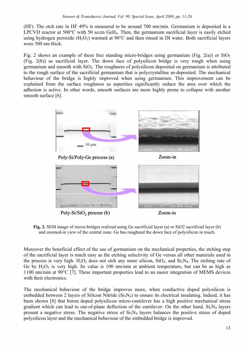
(HF). The etch rate in HF 49% is measured to be around 700 nm/min. Germanium is deposited in a LPCVD reactor at 500°C with 50 sccm GeH4. Then, the germanium sacrificial layer is easily etched using hydrogen peroxide (H2O2) warmed at 90°C and then rinsed in DI water. Both sacrificial layers were 500 nm thick. Fig. 2 shows an example of these free standing micro-bridges using germanium (Fig. 2(a)) or SiO2 (Fig. 2(b)) as sacrificial layer. The down face of polysilicon bridge is very rough when using germanium and smooth with SiO2. The roughness of polysilicon deposited on germanium is attributed to the rough surface of the sacrificial germanium that is polycrystalline as-deposited. The mechanical behaviour of the bridge is highly improved when using germanium. This improvement can be explained from the surface roughness as asperities significantly reduce the area over which the adhesion is active. In other words, smooth surfaces are more highly prone to collapse with another smooth surface [6].
10 µm
Poly-Si/Poly-Ge process (a) Zoom-in
Poly-Si/SiO2 process (b) Zoom-in
10 µm
Poly-Si/Poly-Ge process (a) Zoom-in
Poly-Si/SiO2 process (b) Zoom-in
Fig. 2. SEM image of micro-bridges realized using Ge sacrificial layer (a) or SiO2 sacrificial layer (b)
and zoomed-in view of the central zone. Ge has roughned the down face of polysilicon in touch. Moreover the beneficial effect of the use of germanium on the mechanical properties, the etching step of the sacrificial layer is much easy as the etching selectivity of Ge versus all other materials used in the process is very high. H2O2 does not etch any more silicon, SiO2, and Si3N4. The etching rate of Ge by H2O2 is very high. Its value is 100 nm/min at ambient temperature, but can be as high as 1100 nm/min at 90°C [7]. These important properties lead to an easier integration of MEMS devices with their electronics. The mechanical behaviour of the bridge improves more, when conductive doped polysilicon is embedded between 2 layers of Silicon Nitride (Si3N4) to ensure its electrical insulating. Indeed, it has been shown [8] that boron doped polysilicon micro-cantilever has a high positive mechanical stress gradient which can lead to out-of-plane deflection of the cantilever. On the other hand, Si3N4 layers present a negative stress. The negative stress of Si3N4 layers balances the positive stress of doped polysilicon layer and the mechanical behaviour of the embedded bridge is improved.

Sensors & Transducers Journal, Vol. 90, Special Issue, April 2008, pp. 11-26
14
2.2. SGFET Process Eight masks were designed for the fabrication of the sensor based on classical MOS technology. This sensor has also been developed in low temperature technology (>600°C) on glass by using undoped polysilicon for the channel and highly doped polysilicon for drain and source regions [9]. Both technologies can be developed for N-type or P-type field effect transistors. Fig. 3 presents a scheme of P-type SGFET just before removing the sacrificial layer that is the germanium film. It is nearly a usual MOSFET where the silicon dioxide insulator is replaced by the Ge film. Wafers used are <100> oriented and low-doped N type. The drain and source wells come from nitride boron diffusion at 1100°C with a 650 nm SiO2 as protect layer. The channel is oxidized at 1100°C on 70nm. Then, the channel oxide is protected by a 50nm Si3N4 LPCVD (Low Pressure Chemical Vapor Deposition) layer performed at 600°C. On the nitride layer, a 500nm Ge sacrificial layer is deposited by LPCVD at 550°C, following by a 50 nm silicon nitride layer, which acts as isolation layer for the bottom of the gate. Gate and drain source contacts are silicon thin films amorphously deposited at a temperature of 550°C and a pressure of 90 Pa in a Low Pressure Chemical Vapor Deposition (LPCVD) reactor and are in-situ solid phase crystallized at 600°C. This technology allows depositing boron in situ doped silicon films using a mixture of either silane or disilane, and diborane as doping gas. Previous study [10] showed that a boron doped polysilicon layers deposited from disilane gas that is temperature compatible with diborane gas have good electrical characteristics, with the advantage of a high deposition rate. A last 50 nm silicon nitride layer protects the top of the gate. Vias are opened in the nitride layer for the contact with Aluminium path. Due to the use of liquid ambience, all metal layers are insulated with a last photoresist coat. The last step of the process is the releasing of the gate-bridge by wet etching of the Ge sacrificial layer using hydrogen peroxide (H2O2).
Al
Poly Si P+Ge
Si3N4
Si P+
Bulk Si N
SiO2
Al
Poly Si P+Ge
Si3N4
Si P+
Bulk Si N
SiO2
Fig. 3. Process of the P type SGFET before the releasing of the Ge sacrificial layer.
3. Modeling of Charge Detection Intrinsically, SGFET structure is a sensor of electrical charge that can be present between the bridge and the channel. Indeed, the threshold voltage VTH of MOSFET can be expressed by:
∫ ρ−+ϕ+Φ=oxe
0ox
SCFMSTH dx)x(x
Ce1
CQ
2V , (1)
where ΦMS is the difference between the work function of the gate material and the semiconductor, ϕF is the Fermi level position in the semiconductor versus the mid-gap, QSC is the space charge in the semiconductor, C is the total capacitance between the gate material and the semiconductor, eox is the

Sensors & Transducers Journal, Vol. 90, Special Issue, April 2008, pp. 11-26
15
thickness of the insulator (air-gap, Si3N4 and SiO2), ρ(x) is the charge in the insulator, located at a distance x from the gate. VTH value depends on the charge and on its distribution inside the insulator. In the present SGFET, the gate insulator is a sandwich of 4 layers SiO2, Si3N4, air-gap, Si3N4. For fixed charges in the SiO2 film and both Si3N4 layers, VTH depends on the variation of the charges and their distribution in the air-gap. Moreover this dependence, VTH can change when ΦMS varies due to some chemical reactions at the inner surface of the gate material and at surface of the insulator channel film. Commonly, only this last dependence is considered in historic SGFET. Indeed, when the air-gap is thick, the field effect has a small influence over charges and the distribution of the electrical charge is uniform inside the air-gap. However, the present SGFET shows a very low air-gap, 500 nm, between active layer and gate, implying an important field effect inside the thin air-gap. In this case, the distribution of the electrical charge becomes non-uniform due to high field, leading to a variation of ρ(x). Moreover, the high field can influence the adsorption by shifting the charges on the surface. All these effects lead to a variation of ΦMS but, also, of the last term in the VTH expression. Then, VTH variation can be very large if the effect of high field are considering. However, this effect can occur only with very high fields: we observed a high decrease of the sensibility when the air-gap increases from 500 to 800 nm. The charges sensitivity becomes high due to an increase of charges content accumulated on the surface channel. This accumulation becomes more and more important when the gate-source voltage increases. The modeling is based on the determination of interface charges concentration QSS, depending of the gate voltage [11]. It is the original part of this modeling, this effect being not taken into account in the classical MOS theory. The insulator is supposed to contain constant positive charges concentration, NTOT. These charges are moving under electrical field, due to positive gate VG, and accumulated to the channel surface where there are fixed. The positive charges concentration by surface unit on channel surface QSS, is took proportionally to VG. The variation rate of QSS with VG is proportional to the positive charges concentration NTOT present in the air between gate and channel. We take into account that it needs NLIM = 1014 charges by surface unit to cover completely silicon surface (by taken the silicon atomic density to 5.1022 atom/cm3). In this case, the variation rate of QSS with VG is also proportional to the number of empty places at the silicon surface (qNLIM-QSS) as: ),Q - (qN qN
dVdQ
SSLIMTOTG
SS α= (2)
where α is an experimental factor. From this model, the concentration of accumulated charges in the channel by surface unity, Qn has been calculated and has been drawn in Fig. 4. For few positive charges NTOT in the air between gate and channel, the quantity of accumulated charges in the channel increases slowly versus gate voltage. When the density of positive charges increases, the subthreshold slope decreases, leading a strong increasing of drain current. Finally, when NTOT > 1013 cm-3, there is a value of gate voltage Vg for which the current Ids saturates.

Sensors & Transducers Journal, Vol. 90, Special Issue, April 2008, pp. 11-26
16
0 10 20 30
0.0
5.0x10⁻⁶
1.0x10⁻⁵
1.5x10⁻⁵ NTOT (cm-2)1014
7x10133x1013
1013
1012
1011
1010
Acc
umul
ated
Cha
rge
in th
e ch
anne
l (cb
)
Vg (Volts)0 10 20 30
0.0
5.0x10⁻⁶
1.0x10⁻⁵
1.5x10⁻⁵ NTOT (cm-2)1014
7x10133x1013
1013
1012
1011
1010
Acc
umul
ated
Cha
rge
in th
e ch
anne
l (cb
)
Vg (Volts)
Fig. 4. Accumulated charges in the channel Qn vs. gate voltage for different concentration of positive charges in insulator.
Effect of charges on the air-gap transistor characteristics depends on the density and on the type (positive or negative) of charges Qss. We have summarized the evolution of transfer characteristic for p-type and n-type SGFET in Fig. 5. After introduction of positive Qss, the IDS (VGS) curve of n-type SGFET shifts towards lower voltages (negative shift of the threshold voltage). On the other hand, the presence of negative charges has the contrary effect on the air-gap transistor characteristics: transfer characteristic shifts towards higher voltages (positive shift of the threshold voltage).
Atmosphericair
Introduction of negativecharges
Introduction of positive charges
-5 0 5 10 15 20 25
I ds(A
)
Vg (V)
N-type SGFET
Atmosphericair
Introduction of negativecharges
Introduction of positive charges
-5 0 5 10 15 20 25
I ds(A
)
Vg (V)
N-type SGFET
Atmosphericair
Introduction of positive charges
Introduction of negativecharges
5 0 -5 -10 -15 -20 -25
I ds(A
)
Vg (V)
P-type SGFET
Atmosphericair
Introduction of positive charges
Introduction of negativecharges
5 0 -5 -10 -15 -20 -25
I ds(A
)
Vg (V)
P-type SGFET
(a)
(b)
Fig. 5. Evolution of transfer characteristic of (a) P-type and (b) N-type SGFET after introduction of positive or negative charges.
4. Humidity To check the charge sensitivity of the present SGFET and its modeling, the device is characterized in the air-water mixture with different relative humidity (RH). It is known that the content of negative charges decreases when RH increases.

Sensors & Transducers Journal, Vol. 90, Special Issue, April 2008, pp. 11-26
17
SGFET is placed in a moisture chamber where humidity and temperature are controlled. Transfer characteristics, drain-source current IDS – gate-source voltage VGS of an N-type SGFET, at fixed RH, are plotted in Fig. 6(a). The threshold voltage (Fig. 6(b)) and the subthreshold slope highly decrease and in the same time, IDS saturates at lower gate-source voltage when humidity increases. The threshold voltage shift is more than 18V when the humidity ratio varies from 17 to 70%. The variation is particularly important for low humidity rates. It highlights the high sensitivity of the present sub-micron SGFET. The decrease of VTH is well compatible with the use of N-Type SGFET and the decrease of negative charges when RH increases [12].
-5 0 5 10 15 20 25 3010-11
1x10⁻¹⁰
1x10⁻⁹
1x10⁻⁸
1x10⁻⁷
1x10⁻⁶
1x10⁻⁵ RH
VDS=1V
75%65%
55%50%45%
40%33%
25%
17%
I DS (A
)
VG (V) 20 40 60 80
0
5
10
15
20
V TH (V
)%RH
(a)
(b)
Fig. 6. (a) Transfer characteristic drain-source current IDS – gate-source voltage VGS of a N-type SGFET
for different humidity ratio and( b) threshold voltage versus relative humidity RH. 5. Gas Sensor The detection of humidity confirmed the possibility to use SGFET in charges sensing with high sensitivity. Next step consists to check the SGFET possibility in gas sensing. N-type SGFETs are placed in a stainless steel test chamber (200 ml) where a controlled atmosphere was provided by means of mass flow controllers connected to a computer [13]. The transfer characteristic, drain current versus gate voltage Ids (Vg) at constant drain-source voltage Vds, is measured at room temperature under a flow of synthetic humid air at a flow of 200 ml min-1. Therefore, the gas is introduced at the same flow rate, keeping constant the level of relative humidity. Then the transistor is characterized another time. The SGTFT sensor shows its ability to detect specific gas with a very high sensibility through the examples of the detection of NO2 and NH3. These two gases were chosen for their contrary effect on the threshold voltage shift. Indeed, whereas introducing NH3, the current curve shifted towards lower voltages, i.e. negative shift of the threshold voltage. Introducing NO2 had the reverse effect. Fig. 7(a) shows the variation of transfer characteristics under different NO2 concentrations. The detection is based only on the reaction of NO2 with silicon surface. The molecules of NO2 act as acceptor centres [14]. Once they have been adsorbed on silicon surface, the acceptor-like character would lead to an increase of free carrier (holes) concentration in silicon: negative ions NO-
2 act as negative charges –QSS in gate insulator thus explaining threshold voltage increasing. This negative charges support the known oxidizing character of NO2 [15-16]. Fig. 7(b) shows the variation of transfer characteristics under different NH3 concentrations. The negative shift of the threshold voltage confirms its reducing character [17-18]. The molecules of
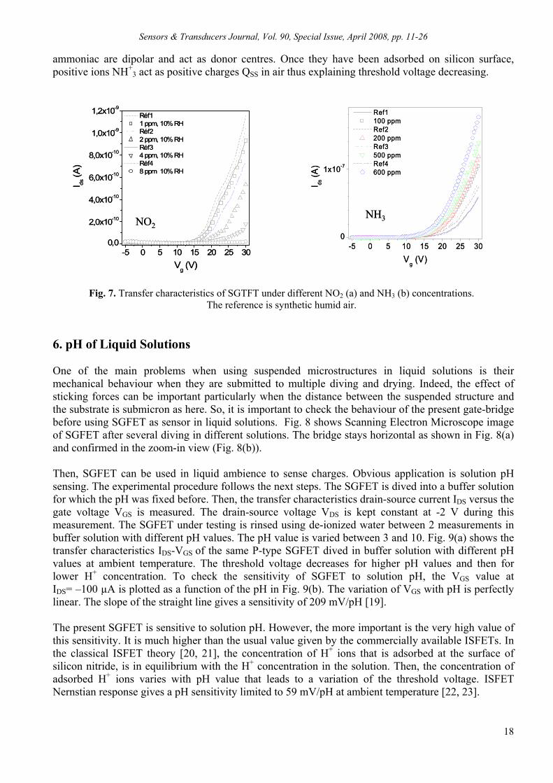
Sensors & Transducers Journal, Vol. 90, Special Issue, April 2008, pp. 11-26
18
ammoniac are dipolar and act as donor centres. Once they have been adsorbed on silicon surface, positive ions NH+
3 act as positive charges QSS in air thus explaining threshold voltage decreasing.
-5 0 5 10 15 20 25 300,0
2,0x10⁻¹⁰
4,0x10⁻¹⁰
6,0x10⁻¹⁰
8,0x10⁻¹⁰
1,0x10⁻⁹
1,2x10⁻⁹
I ds (A
)
Vg (V)
Réf1 1 ppm, 10% RH Réf2 2 ppm, 10% RH Réf3 4 ppm, 10% RH Réf4 8 ppm 10% RH
NO2
-5 0 5 10 15 20 25 300,0
2,0x10⁻¹⁰
4,0x10⁻¹⁰
6,0x10⁻¹⁰
8,0x10⁻¹⁰
1,0x10⁻⁹
1,2x10⁻⁹
I ds (A
)
Vg (V)
Réf1 1 ppm, 10% RH Réf2 2 ppm, 10% RH Réf3 4 ppm, 10% RH Réf4 8 ppm 10% RH
NO2
-5 0 5 10 15 20 25 300
1x10⁻⁷
I ds (A
)
Vg (V)
Ref1 100 ppm Ref2 200 ppm Ref3 500 ppm Ref4 600 ppm
NH3
-5 0 5 10 15 20 25 300
1x10⁻⁷
I ds (A
)
Vg (V)
Ref1 100 ppm Ref2 200 ppm Ref3 500 ppm Ref4 600 ppm
NH3
Fig. 7. Transfer characteristics of SGTFT under different NO2 (a) and NH3 (b) concentrations. The reference is synthetic humid air.
6. pH of Liquid Solutions One of the main problems when using suspended microstructures in liquid solutions is their mechanical behaviour when they are submitted to multiple diving and drying. Indeed, the effect of sticking forces can be important particularly when the distance between the suspended structure and the substrate is submicron as here. So, it is important to check the behaviour of the present gate-bridge before using SGFET as sensor in liquid solutions. Fig. 8 shows Scanning Electron Microscope image of SGFET after several diving in different solutions. The bridge stays horizontal as shown in Fig. 8(a) and confirmed in the zoom-in view (Fig. 8(b)). Then, SGFET can be used in liquid ambience to sense charges. Obvious application is solution pH sensing. The experimental procedure follows the next steps. The SGFET is dived into a buffer solution for which the pH was fixed before. Then, the transfer characteristics drain-source current IDS versus the gate voltage VGS is measured. The drain-source voltage VDS is kept constant at -2 V during this measurement. The SGFET under testing is rinsed using de-ionized water between 2 measurements in buffer solution with different pH values. The pH value is varied between 3 and 10. Fig. 9(a) shows the transfer characteristics IDS-VGS of the same P-type SGFET dived in buffer solution with different pH values at ambient temperature. The threshold voltage decreases for higher pH values and then for lower H+ concentration. To check the sensitivity of SGFET to solution pH, the VGS value at IDS= –100 µA is plotted as a function of the pH in Fig. 9(b). The variation of VGS with pH is perfectly linear. The slope of the straight line gives a sensitivity of 209 mV/pH [19]. The present SGFET is sensitive to solution pH. However, the more important is the very high value of this sensitivity. It is much higher than the usual value given by the commercially available ISFETs. In the classical ISFET theory [20, 21], the concentration of H+ ions that is adsorbed at the surface of silicon nitride, is in equilibrium with the H+ concentration in the solution. Then, the concentration of adsorbed H+ ions varies with pH value that leads to a variation of the threshold voltage. ISFET Nernstian response gives a pH sensitivity limited to 59 mV/pH at ambient temperature [22, 23].
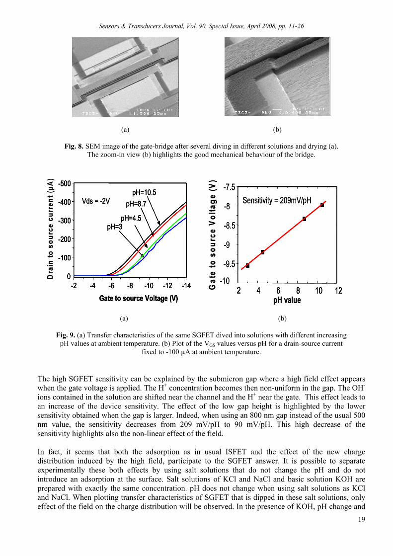
Sensors & Transducers Journal, Vol. 90, Special Issue, April 2008, pp. 11-26
19
(a)
(b)
Fig. 8. SEM image of the gate-bridge after several diving in different solutions and drying (a). The zoom-in view (b) highlights the good mechanical behaviour of the bridge.
pH=10.5pH=8.7
pH=4.5pH=3
Vds = -2V
-2 -4 -6 -8 -10 -12 -140
-100
-200
-300
-400
-500
Dra
in to
sou
rce
curr
ent (
µA)
Gate to source Voltage (V)-2 -4 -6 -8 -10 -12 -14
0
-100
-200
-300
-400
-500
Gate to source Voltage (V)
pH=10.5pH=8.7
pH=4.5pH=3
Vds = -2VpH=10.5
pH=8.7
pH=4.5pH=3
Vds = -2V
-2 -4 -6 -8 -10 -12 -140
-100
-200
-300
-400
-500
Dra
in to
sou
rce
curr
ent (
µA)
Gate to source Voltage (V)-2 -4 -6 -8 -10 -12 -14
0
-100
-200
-300
-400
-500
Gate to source Voltage (V)
Sensitivity = 209mV/pH
2 4 6 8 10 12-10
pH value2 4 6 8 10 12
-9.5
-9
-8.5
-8
-7.5
Gat
e to
sou
rce
Volta
ge (V
)Sensitivity = 209mV/pH
2 4 6 8 10 12-10
pH value2 4 6 8 10 12
-9.5
-9
-8.5
-8
-7.5
Gat
e to
sou
rce
Volta
ge (V
)
(a)
(b)
Fig. 9. (a) Transfer characteristics of the same SGFET dived into solutions with different increasing pH values at ambient temperature. (b) Plot of the VGS values versus pH for a drain-source current
fixed to -100 µA at ambient temperature. The high SGFET sensitivity can be explained by the submicron gap where a high field effect appears when the gate voltage is applied. The H+ concentration becomes then non-uniform in the gap. The OH- ions contained in the solution are shifted near the channel and the H+ near the gate. This effect leads to an increase of the device sensitivity. The effect of the low gap height is highlighted by the lower sensitivity obtained when the gap is larger. Indeed, when using an 800 nm gap instead of the usual 500 nm value, the sensitivity decreases from 209 mV/pH to 90 mV/pH. This high decrease of the sensitivity highlights also the non-linear effect of the field. In fact, it seems that both the adsorption as in usual ISFET and the effect of the new charge distribution induced by the high field, participate to the SGFET answer. It is possible to separate experimentally these both effects by using salt solutions that do not change the pH and do not introduce an adsorption at the surface. Salt solutions of KCl and NaCl and basic solution KOH are prepared with exactly the same concentration. pH does not change when using salt solutions as KCl and NaCl. When plotting transfer characteristics of SGFET that is dipped in these salt solutions, only effect of the field on the charge distribution will be observed. In the presence of KOH, pH change and

Sensors & Transducers Journal, Vol. 90, Special Issue, April 2008, pp. 11-26
20
then both effects of the new distribution of charges inside the gap and of the adsorption will be observed. Fig. 10 shows the transfer characteristics of SGFET dipped in DI water and in solutions of KCl, NaCl and KOH with the same concentration. Similar shift of the characteristics is shown in presence of KCl or NaCl with the same concentration. This shift is only due to the distribution of charges induced by the field inside the gap. VTH shift is induced by the variation of the last term of equation (1). Same charge content gives same shift. With same concentration KOH solution, extra shift is observed. It can be due to the pH of KOH and then to the charges that adsorb at the surface of silicon nitride (first term in equation (1)). Then in presence of KOH the shift is due to both the charge distribution and the adsorbed charge. Both origins contribute to the high pH sensitivity of the present device. Another advantage of the present SGFET consists on the extreme small volume needed to measure the pH. The commercially available ISFETs require a small probe but in combination with a rather large reference electrode. The use of a REFET (identical FET that does not react with the ion concentration, and so covered with insensitive membrane) needs a differential amplifier system [24].
-1 -2 -3 -4 -5 -60,0
-5,0x10⁻⁵
-1,0x10⁻⁴
-1,5x10⁻⁴
-2,0x10⁻⁴
-2,5x10⁻⁴
Id (
A)
Vgs (V)
DI water NaCl KCl KOH
Fig. 10. Transfer characteristics when SGFET is dipped in DI water, and in solutions of NaCl, KCl or KOH. These 3 solutions have the same concentration.
7. Biologic Species Detection The high sensitivity of the submicron SGFET to electrical charges that can be present in liquid solutions opens the way to biologic species detection. Indeed, DNA or proteins electrical sensing consists on the detection of the variation of charges induced by linking between complementary strands of DNA or antigens-antibodies for proteins. These links insure the specificity of the detection in the same time. 7.1. DNA Detection DNA detection systems have opened the field for several years to a very important technological step in the field of knowledge of the genome. The detection system uses the concept of DNA hybridization, where known single strand DNA sequences (probe) are immobilized onto a surface and the complementary DNA strand (target) is recognized by its specific binding affinity. SGFET sensors detection consists to immobilize under the gate well-defined sequences of DNA single strands and to put the device in contact with solution containing the target to be detected. When probes

Sensors & Transducers Journal, Vol. 90, Special Issue, April 2008, pp. 11-26
21
and targets are complementary, the molecular hybridization occurs and the adjunction of negatives charges (brings by phosphate groups) under the gate involves a shift of the threshold voltage VTH of the transistor. Before and after each step of the procedure of the DNA immobilization, SGFET is characterized by plotting its transfer characteristics, Drain-Source current Id as a function of the Gate-Source bias Vg with fixed Drain-Source voltage. This characterization is systematically done with SGFET dipped in the same ambience. Indeed, the transistor characteristic depends on any electrical charge that comes in the space under the bridge. So, it is important to produce a constant ambience that does not change between 2 steps of the procedure. Any variation of the transistor characteristics has to be attributed only to the extra charge coming from the attachment of the DNA. Neutral solution of Phosphate Buffer Saline (PBS) was chosen as constant ambience during the electrical measurements. Fig. 11(a) shows the transfer characteristics when P-type SGFET is dipped in PBS after grafting of 25-mer ODN, after hybridization trying of non-complementary and complementary DNA. A displacement of the characteristic in the direction of the lower negative voltages is observed after hybridization with complementary DNA. It corresponds to the detection of negative charges due to the phosphates groups of the complementary DNA which was grafted (the direction of this displacement is in conformity with the addition of a negative charge for a P-type MOSFET). The shift for a fixed current of -1x10⁻⁵ A is of 0.35V. We also observed that there is a relation between the value of the voltage shift and the concentration of the biological liquid.
-1 -2 -3 -4 -5 -6
0,0
-5,0x10⁻⁶
-1,0x10⁻⁵
-1,5x10⁻⁵
-2,0x10⁻⁵
-2,5x10⁻⁵
-3,0x10⁻⁵
grafted ODN non comp. DNA comp. DNA
Id(A
)
Vg(V)
0.01 0.1 1 10 100 1000
50
100
150
200
250
300
350
Del
taV
(mV)
Log(Concentration ng/µl)
Ids= 25µA
0.01 0.1 1 10 100 1000
50
100
150
200
250
300
350
Del
taV
(mV)
Log(Concentration ng/µl)
Ids= 25µA
(a)
(b)
Fig. 11. (a) Transfer characteristics when SGTFT is dipped in PBS after grafting of ODN, after hybridization trying of non-complementary and complementary DNA. Positive shift shows the presence of negative charge.
(b) Shift of the SGEFET characteristic at constant drain current (25µA) as a function of the target concentration.
Fig. 11(b) shows the increase of the voltage shift of the electrical characteristic taken at fixed drain current (-25 µA) when the concentration of the sequence targets increases. As expected, the curve of the shift as a function of the logarithm of the concentration is perfectly linear (Fig. 11(b)). Remarkably, the sensitivity is constant over 5 decades of concentration. Such large range is unusual with biosensors. Moreover concentration, as weak as 10pg/µl, is detected. Such high sensitivity can open the way for detection without biologic amplification (PCR).
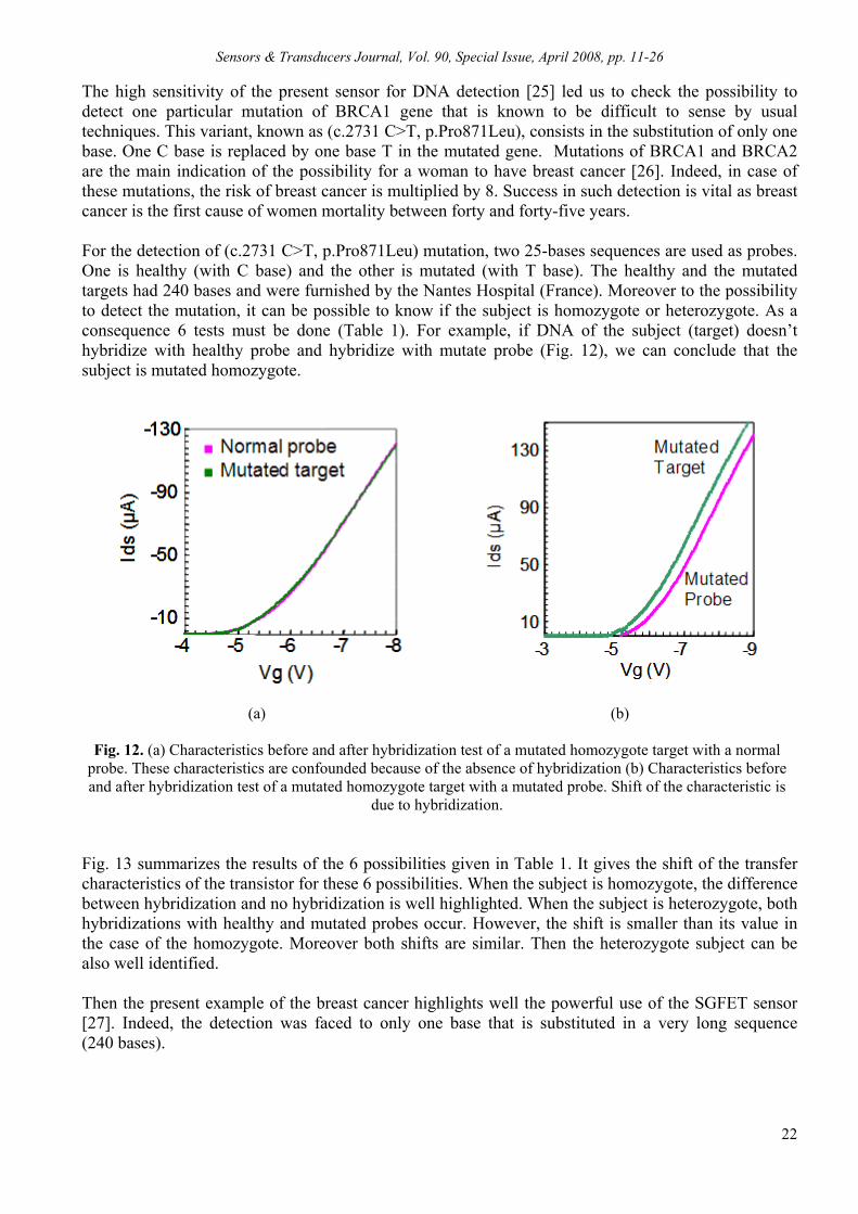
Sensors & Transducers Journal, Vol. 90, Special Issue, April 2008, pp. 11-26
22
The high sensitivity of the present sensor for DNA detection [25] led us to check the possibility to detect one particular mutation of BRCA1 gene that is known to be difficult to sense by usual techniques. This variant, known as (c.2731 C>T, p.Pro871Leu), consists in the substitution of only one base. One C base is replaced by one base T in the mutated gene. Mutations of BRCA1 and BRCA2 are the main indication of the possibility for a woman to have breast cancer [26]. Indeed, in case of these mutations, the risk of breast cancer is multiplied by 8. Success in such detection is vital as breast cancer is the first cause of women mortality between forty and forty-five years. For the detection of (c.2731 C>T, p.Pro871Leu) mutation, two 25-bases sequences are used as probes. One is healthy (with C base) and the other is mutated (with T base). The healthy and the mutated targets had 240 bases and were furnished by the Nantes Hospital (France). Moreover to the possibility to detect the mutation, it can be possible to know if the subject is homozygote or heterozygote. As a consequence 6 tests must be done (Table 1). For example, if DNA of the subject (target) doesn’t hybridize with healthy probe and hybridize with mutate probe (Fig. 12), we can conclude that the subject is mutated homozygote.
(a)
(b)
Fig. 12. (a) Characteristics before and after hybridization test of a mutated homozygote target with a normal probe. These characteristics are confounded because of the absence of hybridization (b) Characteristics before and after hybridization test of a mutated homozygote target with a mutated probe. Shift of the characteristic is
due to hybridization. Fig. 13 summarizes the results of the 6 possibilities given in Table 1. It gives the shift of the transfer characteristics of the transistor for these 6 possibilities. When the subject is homozygote, the difference between hybridization and no hybridization is well highlighted. When the subject is heterozygote, both hybridizations with healthy and mutated probes occur. However, the shift is smaller than its value in the case of the homozygote. Moreover both shifts are similar. Then the heterozygote subject can be also well identified. Then the present example of the breast cancer highlights well the powerful use of the SGFET sensor [27]. Indeed, the detection was faced to only one base that is substituted in a very long sequence (240 bases).

Sensors & Transducers Journal, Vol. 90, Special Issue, April 2008, pp. 11-26
23
Table 1. Prediction of results.
Probe
Target Healthy probe
Mutated probe
Healthy homozygote
Hybridization No Hybridization
Mutated homozygote
No Hybridization
Hybridization
Heterozygote Hybridization Hybridization
MutatedHomozygote
NormalHomozygote
Heterozygote
Shi
ft of
the
char
acte
ristic
s(m
V)
Mutated Probe
Healthy Probe
MutatedHomozygote
NormalHomozygote
Heterozygote
Shi
ft of
the
char
acte
ristic
s(m
V)
Mutated ProbeMutated Probe
Healthy Probe
Fig. 13. Shift of the transfer characteristics of the SGFET for the 6 possibilities given in Table 1. 7.2. Proteins Detection As for DNA detection field, there is high demand in a rapid, low cost and quantitative detection of proteins that can be targeted for diagnosis or prognosis. Indeed, the high cost of the present techniques limits their expanded use into the healthcare system. Here, the selectivity is insured through specific antibodies covalently bound to the surface of SGFET [28]. The example of the detection of transferrin is given here to show the powerful of SGFET in the detection and quantification of proteins. Transferrin is iron-binding glycoprotein. It is the only carrier of iron. It circulates in blood plasma and is produced by the liver. Its level in blood is important to detect iron diseases in the iron metabolism: overload or anemia. Fig. 14 shows the transfer characteristics when SGFET is dipped in PBS after linking antibodies and after specifically linking transferrin to antibodies. Obvious shift of the characteristics is related to the specific attachment and then to the detection of transferrin. 8. Conclusion Submicron Suspended Gate Field Effect Transistor showed its possibility to detect any charge variation under the bridge with very high sensitivity. This sensitivity level was explained and experimentally demonstrated from the effect of the large electrical field that induces new distribution of the charges under the bridge.

Sensors & Transducers Journal, Vol. 90, Special Issue, April 2008, pp. 11-26
24
-4 -6 -80,0
-5,0x10⁻⁵
-1,0x10⁻⁴
Ids
(A)
Vg (V)
Antibodies Antibodies + Transferrin
Fig. 14. Transfer characteristics after linking of antibodies (anti-transferrin) to SGFET surface and after specific linking of transferring on its antibody. Shift of the characteristic is due to specific detection of transferring.
Examples of the use of SGFET to detect humidity, gas, pH of liquid solutions, DNA and proteins were shown to highlight the large range of possibilities offered by this structure. It can work in gaseous or liquid ambience. The example of pH detection is particularly telltale of the high possible sensitivity, 209 mV/pH, as the usual pH sensitivity of usual sensors is known to be theoretically limited to the Nernstian response, 59mV/pH at ambient temperature. The use of submicron SGFET in liquid solutions assumes tacitly that the gate-bridge stays horizontal when the gate bias is applied and when the structure is dipped into liquid and then dried a lot of times. It means that all the technological difficulties were surmounted as shown in this paper. Acknowledgments The Authors wish to thanks all the Microelectronic Group of the IETR, particularly, N. Coulon, R. Rogel, O. De Sagazan Post-Doctoral position, and the previous and present PhD students, H. Kotb, F. Bendriaa, M. Harnois, A.Girard. The authors thank also, C. Guillouzo and A. Corlu from INSERM Rennes (France), P. Brissot and O. Loreal from Rennes Hospital (France), S. Bezieau and V. Guibert from Nantes Hospital (France). This work was partially supported by French Education Ministry and ANR France. References [1]. G. F. Blackburn, M. Levy, J. Janata, Fieldeffect transistor sensitive to dipolar molecules, Appl. Phys. Lett.
43, 1983, pp. 700-701. [2]. B. Flietner, T. Doll, J. Lechner, M Leu, I. Eisele, Fabrication of a hybrid field-effect structure for gas
detection with diverse sensitive materials, Sensors and Actuators B, 8-19, 1994, pp. 632-636. [3]. M. Burgmair, H. P. Frerichs, M. Zimmer, M. Lehmann, I. Eisele, Field effect transducers for work function
gas measurements: device improvements and comparison of performance, Sensors and Actuators B, 95, 2003, pp. 183-188.
[4]. F. Bendriaa, F. Le Bihan, A-C. Salaün, T. Mohammed-Brahim and O. Bonnaud, Study of mechanical maintain of suspended bridge devices used as pH sensor, Journal of Non-Crystalline Solids, Vol. 352, 2006, pp. 1246-1249.

Sensors & Transducers Journal, Vol. 90, Special Issue, April 2008, pp. 11-26
25
[5]. H. M. Kotb, A-C. Salaün, T. Mohammed-Brahim, F. Le Bihan, M. El-Marssi, Polycrystalline silicon thin films for MEMS applications, Thin Solid Films, Vol. 427, 2003, pp. 422-426.
[6]. H. M. Kotb, A-C. Salaün, T. Mohammed-Brahim, N. Coulon, O. Bonnaud and J-Y. Mevellec, High performance polysilicon air-gap thin film transistor on low temperature substrates, SPIE’s International Symposium Microtechnologies for the New Millennium, 2003, Canary Islands, Spain.
[7]. F. Bendriaa, F. Le Bihan, A-C. Salaün, T. Mohammed-Brahim and O. Bonnaud, Study of mechanical maintain of polysilicon air-gap structures used in pH-sensing, ICANS21, 2005, Lisbon, Portugal.
[8]. F. Bendriaa, F. Le Bihan, A. C. Salaün, T. Mohammed-Brahim, O. Bonnaud, Highly sensitive Suspended-Gate Ion Sensitive Transistor for the detection of pH, SPIE’s International Symposium on Microtechnologies for the New Millennium, 2005, Seville, Spain.
[9]. H. Mahfoz - Kotb, A. C. Salaün, T. Mohammed-Brahim, N. Coulon, O. Bonnaud, Air-gap polysilicon thin film transistors on glass substrates, Sensors & Actuators, 2004, A113, pp. 344-349.
[10]. R. Rogel, G. Gautier, N. Coulon, M. Sarret, O. Bonnaud, Influence of precursors gases on LPCVD TFT's characteristics, Thin Solid Films, 2003, 427, pp. 108-112.
[11]. H. Mahfoz-Kotb, A. C. Salaün, F. Bendriaa, F. Le Bihan, T. Mohammed-Brahim and J R Morante, Sensing sensibility of surface micromachined Suspended Gate Polysilicon Thin Film Transistors, Sensors and Actuators B, 2006, Vol. 118, pp. 243-248.
[12]. A-C. Salaün, H. M. Kotb, T. Mohammed-Brahim, F. Le Bihan, H. Lhermite and F. Bendriaa, Suspended-Gate Thin Film Transistor as highly sensitive humidity sensor, SPIE’s International Symposium Microtechnologies for the New Millennium, 2005, Seville, Spain.
[13]. A. Cirera, A. Cabot, A. Cornet and J. R. Morante, CO–CH4 selectivity enhancement by in situ Pd-catalysed microwave SnO2 nanoparticles for gas detectors using active filter, Sensors and Actuators B, 78, 2001, pp. 151-160.
[14]. L. Pancheri, C. J. Oton, Z. Gaburro, G. Soncini, L. Pavesi, Very sensitive porous silicon NO2 sensor, Sensors and Actuators B, 89, 2003, pp. 237-239.
[15]. W Zhang, E. A. de Vasconcelos, H. Uchida, T. Katsube, T. Nakatsubo, and Y. Nishioka, A study of silicon Schottky diode structures for NOx gas detection, Sensors and Actuators B, Vol. 65, 2000, pp. 154-156.
[16]. L Talazac, J Brunet, V Battut, J P Blanc, A Pauly, J Pgermain, S Pellier and C Soulier, Air quality evaluation by monolithic InP-based resistive sensors, Sensors and Actuators B, Vol. 76, 2001, pp. 258-264.
[17]. A. Karthigeyan, R. P. Gupta, K. Scharnagl, M. Burgmair, S. K. Sharma and I. Eisele, A room temperature HSGFET ammonia sensor based on iridium oxide thin film, Sensors and Actuators B, Vol. 85, 2002, pp. 145-153.
[18]. Z. Gergintschew, P. Kornetzky and D. Schipanski, The capacitively controlled field effect transistor CCFET as a new low power gas sensor, Sensors and Actuators B, Vol. 35-36, 1996, pp. 285-289.
[19]. F. Bendriaa, F. Le Bihan, A. C. Salaün, T. Mohammed-Brahim, O. Bonnaud, Highly sensitive Suspended-Gate Ion Sensitive Transistor for the detection of pH, SPIE’s International Symposium on Microtechnologies for the New Millennium, Seville, Spain, 2005.
[20]. P. Bergveld, Development of an ion sensitive solid-state device for neurophysiological measurements, IEEE Trans. Biomed. Eng. 17, 1970, pp. 70-71.
[21]. P. Bergveld, Thirty years of ISFETOLOGY What happened in the past 30 years and may happen in the next 30 years, Sensors and Actuators B, 88, 2003, pp. 1-20.
[22]. S. Martinoia, G. Massobrio, L. Lorenzelli, TModeling ISFET microsensor and ISFET-based Microsystems: a review, Sensors and Actuators B, 105, 2005, pp. 14-27.
[23]. C. Cané, I. Gracia, A. Merlos, Microtechnologies for pH ISFET chemical sensors, Microelectronics Journal, 28, 1997, pp. 389-405.
[24]. C Z. M. Baccar, N. Jaffrezic-Renault, C. Martelet, H. Jaffrezic, G. Marest and A. Plantier, Sodium microsensors based on ISFET/REFET prepared through an ion-implantation process fully compatible with standard silicon technology, Sensors and Actuators B, 32, 1996, pp. 101-105.
[25]. M. Harnois, O. De Sagazan, A. Girard, A-C. Salaün, T. Mohammed-Brahim, Pico concentrated DNA detection by SGFET, Transducers’2007, Lyon, France, 2007.
[26]. Zsofia Kote-Jarai, BRCA1/BRCA2 mutation status and nalysis of cancer family history in participants of the Royal Marsden Hospital tamoxifen chemoprevention trial, Cancer Letters, 247, 2007, pp. 259–265.
[27]. M. Harnois, O. De Sagazan, A. C. Salaün, T. Mohammed-Brahim, S. Bezieau, Using Highly Sensitive Suspended-Gate Field Effect Transistor in the DNA Detection: Application to Breast Cancer Diagnose, 2nd International Conference on Sensing Technology, Palmerston North - New Zealand, Nov. 26-28, 2007.

Sensors & Transducers Journal, Vol. 90, Special Issue, April 2008, pp. 11-26
26
[28]. A. Girard, F. Bendriaa, O. De Sagazan, M. Harnois, F. Le Bihan, P. Brissot, O. Loréal, A-C. Salaün, T. Mohammed-Brahim, Transferrin electronic detector for iron disease diagnostics, 5th IEEE International Conference on Sensors, Daegu - Korea, Oct. 22 – 25, 2006.
___________________
2008 Copyright ©, International Frequency Sensor Association (IFSA). All rights reserved. (http://www.sensorsportal.com)

Sensors & Transducers Journal, Vol. 90, Special Issue, April 2008, pp. 27-38
27
SSSeeennnsssooorrrsss &&& TTTrrraaannnsssddduuuccceeerrrsss
ISSN 1726-5479© 2008 by IFSA
http://www.sensorsportal.com
Estimation of Low Concentration Magnetic Fluid Weight Density and Detection inside an Artificial Medium
Using a Novel GMR Sensor
Chinthaka GOONERATNE, *Agnieszka ŁEKAWA, Masayoshi IWAHARA, Makiko KAKIKAWA and Sotoshi YAMADA
Kanazawa University, Kakuma-machi, Kanazawa, Ishikawa 920-1192, Japan *Lublin University of Technology, Lublin, Poland
E-mail: [email protected], [email protected]
Received: 15 October 2007 /Accepted: 20 February 2008 /Published: 15 April 2008 Abstract: Hyperthermia treatment has been gaining momentum in the past few years as a possible method to manage cancer. Cancer cells are different to normal cells in many ways including how they react to heat. Due to this difference it is possible for hyperthermia treatment to destroy cancer cells without harming the healthy normal cells surrounding the tumor. Magnetic particles injected into the body generate heat by hysteresis loss and temperature is increased when a time varying external magnetic field is applied. Successful treatment depends on how efficiently the heat is controlled. Thus, it is very important to estimate the magnetic fluid density in the body. Experimental apparatus designed for testing, numerical analysis, and results obtained by experimentation using a simple yet novel and minimally invasive needle type spin-valve giant magnetoresistance (SV-GMR) sensor, to estimate low concentration magnetic fluid weight density and detection of magnetic fluid in a reference medium is reported. Copyright © 2008 IFSA. Keywords: Hyperthermia treatment, SV-GMR sensor, Low-invasive, Magnetic fluid, Demagnetizing factor 1. Introduction The utilization of magnetic nanoparticles has been proposed for a diverse range of potential applications such as in the fields of electronics, biomedicine, energy, military uses and waste management, for several years. With the recent advancements in nanotechnology, smart sensors have been used

Sensors & Transducers Journal, Vol. 90, Special Issue, April 2008, pp. 27-38
28
extensively in explicit biomedical applications [1]. Hyperthermia treatment has the potential to be an effective tool for healing cancer. The principle behind hyperthermia treatment lies in the fact that cancer cells are more sensitive to heat than normal healthy cells [2]. While it has been known for some time that heat does shrink tumors it is only recently that safe ways have been found to raise body temperature in a safe and effective manner. Thus, hyperthermia treatment can be used effectively to kill or weaken cancer cells with negligible effects on healthy cells. The many advantages of this type of treatment include no side effects or pain for the patient, minimally invasive and less treatment time, compared to treatments such as chemotherapy and radiotherapy, and even though the cancer cells do not die completely they may be become more susceptible to treatments such as ionizing radiation or chemotherapy, allowing such therapy to be given in small doses [3]. Magnetic fluid with magnetic nano-particles is injected into the affected area. Magnetic particles generate heat by hysteresis loss and temperature is increased when a time varying external magnetic field is applied [4]. The movement of the magnetic particles can be controlled by external magnetic fields, which means it can be directed to an area of interest, held there until treatment concludes and then removed. As a result of external magnetic fields the temperature of the magnetic nano-particles increases, due to eddy current loss [5]. Given sufficient heat it is possible to destroy or partly destroy cancer cells in the affected area. The amount of nano-particles inside the body must be verified before treatment so that healthy cells won’t be affected. Once the magnetic fluid is injected it spreads throughout the tissue decreasing the content density. Magnetic density is then needed to be confirmed once inside the tissue. The needle type spin valve giant magnetoresistance (SV-GMR) sensor is proposed to estimate low concentration magnetic fluid content density inside the body in a minimal, low invasive way. 2. Principles of Hyperthermia Treatment Lately hyperthermia has been shown to be a possible cancer therapy based on induction heating [4, 5]. The sensitivity of cancer cells to heat compared with healthy cells paves the way for effective cancer management using hyperthermia treatment. Dextran magnetite (DM) is a complex of dextran and superfine iron oxide particles, and this complex is stable as a colloid without aggregation or deposition in various solvents or serum [6]. As shown in Fig. 1, DM is injected into the affected area in the body and brought close to the cancerous cells.
Tower PC
Control device andpower supply
Exciting coil supplyingmagnetic fields
Magnetic fluid (DM)filled cancer or tumor
Fig. 1. Hyperthermia treatment as a cancer therapy.

Sensors & Transducers Journal, Vol. 90, Special Issue, April 2008, pp. 27-38
29
The nano-particles heat up to around 42.5 °C due to the external AC magnetic fields that are acted upon the tumor [7]. Tumor tissues are heated directly since hysteresis loss is induced. Exposure to such heat for a given time will kill or partly destroy tumor tissue, where the latter can be utilized for giving low doses of other treatments such as X-ray therapy. The heat capacity, Q (W/ml) generated by magnetite can be calculated as follows: 2
m wQ k fD B= , (1) where f ; exciting frequency (kHz), Dw; magnetic fluid weight density (mgFe/ml), B ; applied magnetic flux density amplitude (T), Km; 3.14×10³ (W/Hz/(mgFe/ml)/T2/ml). The value of the constant km was obtained by experiment, where an exciting magnetic flux at frequency 158 kHz was applied to Resovist®, a substance with a magnetic weight density of 28 mgFe/ml. It can be seen from Eq. (1) that all parameters except the magnetic fluid weight density (Dw) are generally known. When DM is injected into the affected area it spreads inside the cancer tissue effectively decreasing the magnetic fluid weight density [7-9]. So to control the heat in hyperthermia treatment it is important to verify Dw. 3. Analytical Estimation of Magnetic Fluid Content Density 3.1. Relationship between Relative Permeability and Magnetic Fluid Weight Density The relative permeability of the magnetic fluid can be estimated by measuring the magnetic flux density in tissue injected with magnetic fluid. A relationship is established between the magnetic fluid weight density and relative permeability. Based on this relationship the magnetic fluid volume density, Dv, is calculated. The magnetic fluid weight density is estimated as f v
wv f v
DD
(1 D ) Dγ
γ×
=− + ×
, (2)
simplified and rearranged to obtain the magnetic fluid volume density as,
v
fw
1D11 1
Dγ
=⎛ ⎞⎛ ⎞
+ −⎜ ⎟⎜ ⎟⎜ ⎟⎝ ⎠⎝ ⎠
, (3)
where γf = 4.58 (W-35 sample – Taiho Co.) and is the specific gravity of magnetic bead. Magnetic nano-particles are assumed to have a cylindrical shape with equal height and diameter, and that they are uniformly distributed in the fluid. Furthermore, it is assumed that the nano-particles have an infinite permeability and water has one. Magnetic fluid density can be estimated based on the prediction of the magnetic field path when the fluid is placed under a uniform magnetic flux density. Two equivalent magentic paths, with and without magntic particles, are considered. Then an equation is obtained for the relative permeability derived from the equivalent magnetic permeance of one cubic meter [8,9]. So then the relative permeability, µ*, of magnetic fluid as a bulk is estimated as
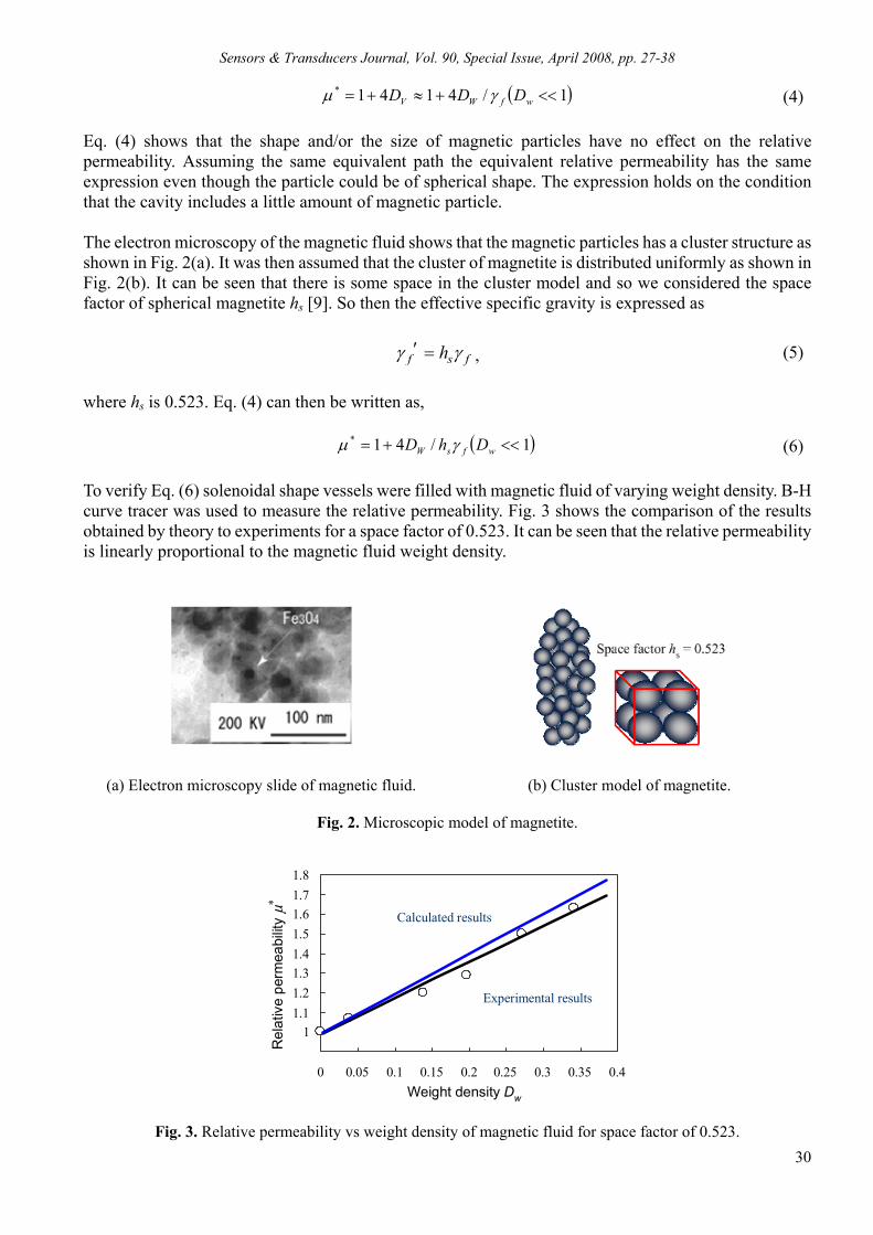
Sensors & Transducers Journal, Vol. 90, Special Issue, April 2008, pp. 27-38
30
( )1/4141* <<+≈+= wfWV DDD γµ (4) Eq. (4) shows that the shape and/or the size of magnetic particles have no effect on the relative permeability. Assuming the same equivalent path the equivalent relative permeability has the same expression even though the particle could be of spherical shape. The expression holds on the condition that the cavity includes a little amount of magnetic particle. The electron microscopy of the magnetic fluid shows that the magnetic particles has a cluster structure as shown in Fig. 2(a). It was then assumed that the cluster of magnetite is distributed uniformly as shown in Fig. 2(b). It can be seen that there is some space in the cluster model and so we considered the space factor of spherical magnetite hs [9]. So then the effective specific gravity is expressed as
f s fhγ γ′ = , (5)
where hs is 0.523. Eq. (4) can then be written as, ( )1/41* <<+= wfsW DhD γµ (6) To verify Eq. (6) solenoidal shape vessels were filled with magnetic fluid of varying weight density. B-H curve tracer was used to measure the relative permeability. Fig. 3 shows the comparison of the results obtained by theory to experiments for a space factor of 0.523. It can be seen that the relative permeability is linearly proportional to the magnetic fluid weight density.
(a) Electron microscopy slide of magnetic fluid.
(b) Cluster model of magnetite.
Fig. 2. Microscopic model of magnetite.
0.91
1.11.21.31.41.51.61.71.8
0 0.05 0.1 0.15 0.2 0.25 0.3 0.35 0.4Weight density Dw
Experimental results
Calculated results
0.91
1.11.21.31.41.51.61.71.8
0 0.05 0.1 0.15 0.2 0.25 0.3 0.35 0.4Weight density Dw
Experimental results
Calculated results
Rel
ativ
e pe
rmea
bilit
y µ*
Weight density Dw
Fig. 3. Relative permeability vs weight density of magnetic fluid for space factor of 0.523.

Sensors & Transducers Journal, Vol. 90, Special Issue, April 2008, pp. 27-38
31
3.2. Magnetic Flux Density Inside and Outside a Magnetic Fluid Filled Cavity under Uniform Magnetic Fields Fig. 4 shows a magnetic fluid filled cavity placed under a uniform magnetic flux density. Flux lines will then concentrate at the magnetic fluid filled cavity, which is assumed to have permeability slightly greater than one.
B0
B1B1
Uniform magnetic fluxdensity outside magnetic
fluid filled cavity
Magnetic fluidfilled cavity
Magnetic flux densityinside magnetic fluid
filled cavity
Fig. 4. Model showing magnetic flux distribution inside an embedded cavity. If a magnetic flux, B0, is applied then the flux in the cavity is assumed as B1. The magnetic flux density inside the magnetic fluid filled cavity, B1, will change according to the content density of the magnetic fluid. The magnetic flux at the centre of the cavity, B1, can be expressed according to the following equation: *
01 *
BB
1 N( 1)µµ
=+ −
, (7)
where µ* is the relative permeability which is assumed as slightly greater than 1 and N is the demagnetizing factor of the cavity. Substituting Eq. (4) for Eq. (7), we get, 1 0
v0
B B( 1 N )4D
B−
≅ − (8)
From Eq. (8) it can be seen that from the difference between the applied flux, B0, and the flux in the magnetic fluid, B1, the volume density and thus the weight density of the magnetic fluid can be estimated. The change between the applied magnetic flux and the flux in the container is directly proportional to the magnetic fluid volume density. 3.3 Helmholtz Tri-coil and Uniform Magnetic Flux Density Helmholtz coils are used in a variety of applications, primarily due to its ability to produce a relatively uniform field configuration, ease of construction and flexibility [10, 11]. Fig. 5 shows the designed Helmholtz tri-coil. The parameters are: a = 770 mm, b = 260 mm, c = 214 mm, h = 315 mm, N1, N2 and N3 are 140, 4 and 1 turns respectively. In biomedical applications low concentration magnetic fluid (typically less than 2.8 % weight density) is used. To clearly differentiate between magnetic fluid at low weight densities it is essential that the error from the midpoint in the uniform region is very low. The
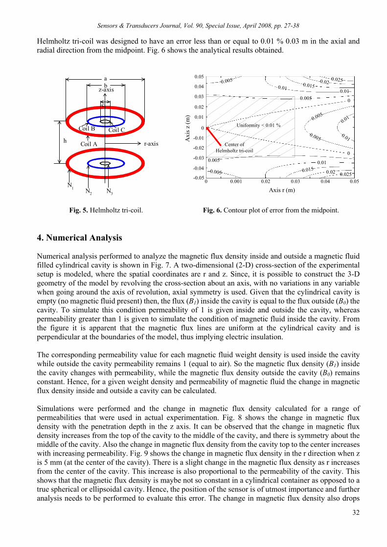
Sensors & Transducers Journal, Vol. 90, Special Issue, April 2008, pp. 27-38
32
Helmholtz tri-coil was designed to have an error less than or equal to 0.01 % 0.03 m in the axial and radial direction from the midpoint. Fig. 6 shows the analytical results obtained.
ab
c
h
N1 N2 N3
Coil A
Coil B Coil C
z-axis
r-axis
0 0.001 0.02 0.03 0.04 0.05
0
-0.05
-0.04
-0.03
-0.02
-0.01
0.01
0.02
0.03
0.04
0.05
0.005
0.005
0.005
0.005
0.005 0.01
0.01
0.01
0.015
0.01
0.01
0.015
0.02
0.020.025
0.025
0.005
0
0
Axi
s z (m
)Axis r (m)
Center ofHelmholtz tri-coil
Uniformity < 0.01 %
Fig. 5. Helmholtz tri-coil.
Fig. 6. Contour plot of error from the midpoint.
4. Numerical Analysis Numerical analysis performed to analyze the magnetic flux density inside and outside a magnetic fluid filled cylindrical cavity is shown in Fig. 7. A two-dimensional (2-D) cross-section of the experimental setup is modeled, where the spatial coordinates are r and z. Since, it is possible to construct the 3-D geometry of the model by revolving the cross-section about an axis, with no variations in any variable when going around the axis of revolution, axial symmetry is used. Given that the cylindrical cavity is empty (no magnetic fluid present) then, the flux (B1) inside the cavity is equal to the flux outside (B0) the cavity. To simulate this condition permeability of 1 is given inside and outside the cavity, whereas permeability greater than 1 is given to simulate the condition of magnetic fluid inside the cavity. From the figure it is apparent that the magnetic flux lines are uniform at the cylindrical cavity and is perpendicular at the boundaries of the model, thus implying electric insulation. The corresponding permeability value for each magnetic fluid weight density is used inside the cavity while outside the cavity permeability remains 1 (equal to air). So the magnetic flux density (B1) inside the cavity changes with permeability, while the magnetic flux density outside the cavity (B0) remains constant. Hence, for a given weight density and permeability of magnetic fluid the change in magnetic flux density inside and outside a cavity can be calculated. Simulations were performed and the change in magnetic flux density calculated for a range of permeabilities that were used in actual experimentation. Fig. 8 shows the change in magnetic flux density with the penetration depth in the z axis. It can be observed that the change in magnetic flux density increases from the top of the cavity to the middle of the cavity, and there is symmetry about the middle of the cavity. Also the change in magnetic flux density from the cavity top to the center increases with increasing permeability. Fig. 9 shows the change in magnetic flux density in the r direction when z is 5 mm (at the center of the cavity). There is a slight change in the magnetic flux density as r increases from the center of the cavity. This increase is also proportional to the permeability of the cavity. This shows that the magnetic flux density is maybe not so constant in a cylindrical container as opposed to a true spherical or ellipsoidal cavity. Hence, the position of the sensor is of utmost importance and further analysis needs to be performed to evaluate this error. The change in magnetic flux density also drops

Sensors & Transducers Journal, Vol. 90, Special Issue, April 2008, pp. 27-38
33
rapidly at 8 mm. This is due to the fact that according to the cavity dimensions (height: 10 mm and radius: 8 mm) the position that the magnetic flux density drops rapidly is a boundary of the cavity.
Helmholtz tri-coil
Helmholtz tri-coil
Magnetic flux densityinside the cavity
(B1)z
r
Magnetic flux densityoutside the cavity
(B0)
0.2
0.4
0.6
0.8
1.0
Min 1.076 e-6
Max 1.102 e-3Ч 10-3
Streamline: Magnetic Flux Density [T]
0.008 m
0.01
m
Fig. 7. FEMLAB simulation model.
0
0.2
0.4
0.6
0.8
1
1.2
0 1 2 3 4 5 6 7 8 9 10
P=1.00403 P1.00603 P=1.00802 P1.01367 P=1.01901
0 2 4 6 8 100
0.2
0.4
0.6
0.8
1
1.2
Center ofcavity
Penetration depth in z-direction (mm)
Cha
nge
in m
agne
tic fl
ux d
ensi
ty (%
)
Fig. 8. Change in magnetic flux density in the z direction.

Sensors & Transducers Journal, Vol. 90, Special Issue, April 2008, pp. 27-38
34
0
0.2
0.4
0.6
0.8
1
1.2
1.4
0 1 2 3 4 5 6 7 8
P1.00403 P1.00603 P1.00802 P1.01367 P1.01901
0
0.2
0.4
0.6
0.8
1
1.2
02 4 6 8
1.4
r-direction (mm)
Cha
nge
in m
agne
tic fl
ux d
ensi
ty (%
)
Fig. 9. Change in magnetic flux density in the r direction (from center of cavity). 5. Experimental Analysis 5.1. SV-GMR Sensor and Experimental Setup The needle type SV-GMR sensor and the experimental setup used to estimate the magnetic fluid weight density is shown in Fig. 10. By measuring the applied flux density (outside of the cavity) and the magnetic flux density inside the magnetic fluid filled cavity the magnetic fluid weight density can be estimated. The SV-GMR sensor is especially fabricated for testing inside the body in a simple and a minimally low invasive way. The SV-GMR element with sensing area of 75 µm × 40µm is at the tip of the needle. The sensing direction is parallel to the needle. A constant current of 5 mA is applied to the SV-GMR sensor. The small signal characteristics of the sensor at 1 kHz is shown in Fig. 11. The sensitivity is approximately 12.5 µV/µT. Magnetic fluid is injected into cavity of 16 mm diameter and 10 mm height. The Helmholtz tri-coil is used to produce uniform magnetic flux of 100 µT at 100 Hz. The SV-GMR sensor needle tip is placed in the middle of the Helmholtz coil and the cavity is moved so that the needle tip is in the centre of the cavity.
Tray with cylindricalembedded cavity
Needle typeprobe
Helmholtz tri-coilSensing axis
Tip of needle-type probe
Cover
Needle type probeL = 15 mm
Probe connector
Fig. 10. Experimental setup.

Sensors & Transducers Journal, Vol. 90, Special Issue, April 2008, pp. 27-38
35
Fig. 11. Small signal ac characteristics of needle-type SV-GMR sensor at 1 kHz. 5.2. Estimation of Low Concentration Magnetic Fluid Weight Density The volume density of DM used in medical applications such as in hyperthermia treatment is less than 1.2 %. So it is important to measure low concentration DM inside the body before as well as after treatment. Fig. 12 show the experimental results obtained. The relationship between the magnetic fluid weight density and the change in magnetic flux density is obtained. The relationship between the change in magnetic flux density and the magnetic fluid weight density is linear and proportional.
Fig. 12. Experimental results estimating low concentration magnetic fluid weight density. 5.3. Detection of Magnetic Fluid inside Agar Experiments were performed to simulate potential in-vivo experimentation. A concentration of agar and magnetic fluid was made (5 % agar, 5 % magnetic fluid and 90 % distilled water) and cooled to solidify.

Sensors & Transducers Journal, Vol. 90, Special Issue, April 2008, pp. 27-38
36
Then, potato starch was made and the solidified agar pieces were inserted into the potato starch as shown in Fig. 13. Experiments were performed with the needle-type SV-GMR sensor to estimate the magnetic fluid filled cylindrical agar pieces (diameter 16 mm and height 10 mm) that were inserted in potato starch. The demagnetizing factor of a cavity depends on the ratio of height to diameter of cavity (m). The sensor needle was applied to the middle of the agar pieces and the results are shown below in Fig. 14 for weight density percentages of 0.24, 0.36, 0.47 and 0.81. The result obtained here is only the amplitude of the signal corresponding to the magnetic flux density inside the magnetic fluid. The change in signal is the difference between the signal obtained inside the magnetic fluid and in potato starch (reference medium). It can be seen that the change in signal increases with increasing magnetic fluid weight density.
Potato starch medium
Plastic box
Magnetic fluid filled agar pieces
Top-view of model
Fig. 13. Top-view model of magnetic fluid and potato starch.
0
0.01
0.02
0.03
0.04
0.05
1 2 3 4 5 6 7 8 9 10 11 12 13 14 15 16 17 18 19 20 21Position (cm)
Cha
nge
in S
igna
l (m
V)
Dw = 0.24 % Dw = 0.36 %
Dw = 0.47 %
Dw = 0.81 %
m = 0.625
Center ofmagnetic fluid
Potato starch medium
2 cm 5 cm5 cm
5 cm
5 cm
10cm
16 mm
10 m
m
m = 0.625
Fig. 14. Detection of magnetic fluid of varying densities.
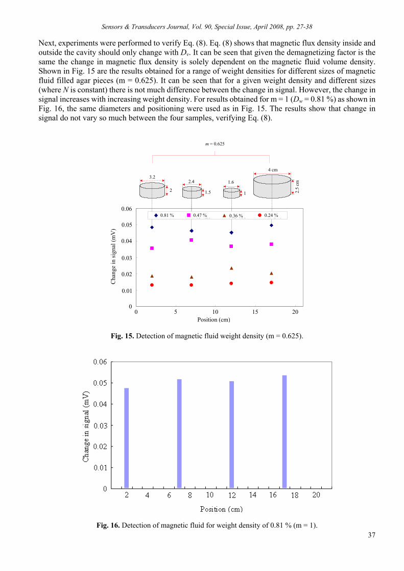
Sensors & Transducers Journal, Vol. 90, Special Issue, April 2008, pp. 27-38
37
Next, experiments were performed to verify Eq. (8). Eq. (8) shows that magnetic flux density inside and outside the cavity should only change with Dv. It can be seen that given the demagnetizing factor is the same the change in magnetic flux density is solely dependent on the magnetic fluid volume density. Shown in Fig. 15 are the results obtained for a range of weight densities for different sizes of magnetic fluid filled agar pieces (m = 0.625). It can be seen that for a given weight density and different sizes (where N is constant) there is not much difference between the change in signal. However, the change in signal increases with increasing weight density. For results obtained for m = 1 (Dw = 0.81 %) as shown in Fig. 16, the same diameters and positioning were used as in Fig. 15. The results show that change in signal do not vary so much between the four samples, verifying Eq. (8).
0
0.01
0.02
0.03
0.04
0.05
0.06
0 5 10 15 20
1 to 70 1 to 120 1 to 160 1 to 240
2.5
cm
4 cm
1.6
1
2.4
1.5
3.2
2
m = 0.625
0.81 % 0.47 % 0.36 % 0.24 %
0 5 10 15 20
0.01
0.02
0.03
0.04
0.05
0.06
0
Position (cm)
Cha
nge
in si
gnal
(mV
)
Fig. 15. Detection of magnetic fluid weight density (m = 0.625).
Fig. 16. Detection of magnetic fluid for weight density of 0.81 % (m = 1).

Sensors & Transducers Journal, Vol. 90, Special Issue, April 2008, pp. 27-38
38
5. Conclusions A novel needle type spin-valve giant magnetoresistance sensor is proposed for estimating the low concentration magnetic fluid weight density, which is prevalent in the biomedical field. The control of heat is critical in hyperthermia treatment so it is essential to verify the magnetic fluid weight density once inside the body before and after treatment. The relationship between the change in magnetic flux density inside and outside a magnetic fluid cavity has been shown by experimentation. Experiments were also performed to estimate magnetic fluid filled agar pieces inside potato starch reference medium. The experiments showed that magnetic fluid inside a reference medium can be estimated and shape of the cavity does not affect the magnetic flux density inside the magnetic fluid filled agar pieces. The results show that the proposed technique can be applied to biomedical engineering such as in the confirmation of magnetic fluid density injected into human body for cancer treatment by means of hyperthermia therapy, based on induction heating technique. References [1]. G. L. Cote, R. M. Lec, M. V. Pishko, Emerging Biomedical Sensing Technologies and Their Applications,
IEEE Sensors Journal, Vol. 3, No. 3, June 2003, pp. 251-266. [2]. M. H. Falk, R. D. Issels, Hyperthermia in Oncology, International Journal of Hyperthermia, 17, 1, Jan.-Feb.
2001, pp. 1-18. [3]. J. van der Zee, Heating the patient: a promising approach ?, Annals of Oncology, 13, 8, August 2002,
pp. 1173-1184. [4]. R. Hergt, W. Andra, C. G. d’Ambly, I. Hilger, W. A. Kaiser, U. Richter, and H. G. Schmidt, Physical Limits
of Hyperthermia Using Magnetic Fine Particles, IEEE Transactions on Magnetics, Vol. 34, No. 5, Sept. 1998, pp. 3745-3754.
[5]. K. Tazawa, I. Nagano, Development of a portable inductive heating system using dextran magnetite, Journal of Hyperthermia Oncology Phys. D: Appl. Phys. London, Vol. 19, Feb. 2003, pp. 79-85.
[6]. Nagano, H. Nagae, S. Shiozaki, I. Kawajiri, S. Ygitani, K. Katayama, and K. Tazawa, Development of a portable cancer treatment system using induction heating: a new weapon for killing the cancer, 2nd Kanazawa workshop, Mar. 2006, pp. 11-15.
[7]. S. C. Mukhopadhyay, K. Chomsuwan, C. P. Gooneratne and S. Yamada, A novel needle-type SV-GMR sensor for bio-medical applications, IEEE Sensors Journal, Vol. 7, Issue 3, Mar. 2007, pp. 401-408.
[8]. S. Yamada, K. Chomsuwan, S. C. Mukhopadhyay, M. Iwahara, M. Kakikawa, and I. Nagano, Detection of Magnetic Fluid Volume Density with SV-GMR Sensor, Journal of the Magnetics Society of Japan, Vol. 31, No. 2, 2007, pp. 44-47.
[9]. C. Gooneratne, A. Lekawa, M. Iwahara, M. Kakikawa, and S. Yamada, Novel Needle Type GMR Sensor Application in Hyperthermia Therapy, Proceedings of the 2nd International Conference on Sensing Technology (ICST 07), Nov. 26-28, 2007, Palmerston North, New Zealand, pp. 595-600.
[10]. J. Wang, S. She, S. Zhang, An improved Helmholtz coil and analysis of its magnetic field homogeneity, Review of Scientific Instruments, Vol. 73, No. 5, May 2002, pp. 2175-2179.
[11]. Sasada, Y. Nakashima, A planar coil system consisting of three coil pairs for producing uniform magnetic field, Journal of Applied Physics, Vol. 99, Issue 8, 2006, pp. 08D904 – 08D904-3.
___________________
2008 Copyright ©, International Frequency Sensor Association (IFSA). All rights reserved. (http://www.sensorsportal.com)
Sensors & Transducers Journal, Vol. 90, Special Issue, April 2008, pp. 39-47
39
SSSeeennnsssooorrrsss &&& TTTrrraaannnsssddduuuccceeerrrsss
ISSN 1726-5479© 2008 by IFSA
http://www.sensorsportal.com
Design of an Enhanced Electric Field Sensor Circuit in 0.18 µm CMOS for a Lab-on-a-Chip Bio-cell Detection Micro-Array
S. M. Rezaul HASAN and Siti Noorjannah IBRAHIM
Center for Research in Analog and VLSI microsystem dEsign (CRAVE), Massey University, Auckland 1311, New Zealand
E-mail: [email protected], [email protected]
Received: 15 October 2007 /Accepted: 20 February 2008 /Published: 15 April 2008 Abstract: An improved CMOS Electric-Field Sensor circuit for sensing bio-cells is presented. The sensor can be used in a Lab-on-a-chip micro-array that uses dielectrophoretic actuation for detecting bio-cells. Compared to the previously published design (DeFET), this improved circuit utilizes the current in both branches of the DeFET to provide a much larger output sensed voltage for the same input electric field intensity (V/m). The enhanced circuit indicates several orders higher electric field sensitivity based on the same 0.18 µm CMOS technology. In general, the improved circuit is found to provide 30dB higher sensitivity relative to the previous DeFET circuit. Copyright © 2008 IFSA. Keywords: Electric-field sensor, Dielectrophoresis, Bio-cells, Lab-on-a-chip 1. Introduction Biological analysis at a miniaturized scale leading to Lab-on-a-chip [1], [4] is an area of immense current research focus in the emerging field of micro-bioelectronics and micro-biotechnology. Sensing and sorting the presence of biological cells and/or organic macro-molecules is an important aspect of today’s efforts in miniaturized biotechnological devices and monolithic systems. There are many existing techniques for determining the presence and concentration of cells or bio-macromolecules e.g., MEMS devices, ultra-sound, magnetic sorting and dielectrophoresis [5]. Dielectrophoretic levitation technique [1], [3], [4] using a non-uniform electric field has recently gained considerable attention in Lab-on-a-chip applications, particularly for biological elements which are less than 1 µm in diameter such as virus, bacteria and protein molecules. These microbes and sub-microbes being very susceptible to contamination and membrane rupture are well suited to dielectrophoretic detection

Sensors & Transducers Journal, Vol. 90, Special Issue, April 2008, pp. 39-47
40
techniques. For dielectrophoretic actuation [1], an applied non-uniform electric field creates a dipole on the biocell and forces the biocell dipoles to concentrate either towards the region of lower electric field concentration (negative dielectrophoresis) if the cell has lower dielectric polarizability compared to the surrounding medium or towards the region of higher electric field concentration (positive dielectrophoresis) if the cell has higher dielectric polarizability compared to the surrounding medium. The sensing part of dielectrophoretic analysis has been carried out mostly using either the optical technique [6] or the impedance sensing technique [7]. However, there is a more direct method of sensing in dielectrophoretic analysis which involves the detection of the change in the original applied electric field concentration due to the presence and the concentration distribution of the bio-cells. The authors in [1], [2] describes a suitable CMOS differential electric field sensitive Field Effect Transistor (DeFET) device for detecting changes in the gradient of the non-uniform electric field in any particular location (spot) in a single-chip miniaturized Lab-on-a-chip system. In this paper, the DeFET design presented in [1] and [2] is considerably improved which is called an enhanced DeFET (EDeFET) circuit where the currents in both the branches of the DeFET device are utilized to provide higher sensitivity. Preliminary work on this proposed circuit was reported in [8]. 2. Enhanced DeFET Circuit Fig. 1 shows the originally proposed CMOS DeFET circuit [1], [2] which consists of non-uniform electric field being applied across the inputs Vin1 and Vin2. The difference between Vin1 and Vin2 reflects the intensity of the electric field. Vin1 and Vin2 connect to two sets of cross-coupled complementary devices. This connection causes the overdrives of both the PMOS and NMOS devices of one branch to go up as the overdrives of both the PMOS and NMOS devices of the other branch goes down. The applied electric field (using a set of electrodes) can be considered as a bias electric field which keeps all the PMOS and NMOS channels ON preferably in the saturation region (for sensing linearity). Changing electric field intensity will cause Vin1 and Vin2 to move in opposite directions (one increasing and one decreasing). As a result, current in the branch M1and M4 will go up when the current in the branch M2and M3 goes down and vice versa. Consequently, this widening differential current between the two branches can be exploited to detect small variations in the electric field intensity. However, in the original circuit this differential current is not exploited to obtain a higher possible sensitivity to electric field intensity variations.
Fig. 1. A CMOS differential electric field sensitive field effect transistor (DeFET) for non-uniform electric field sensing.

Sensors & Transducers Journal, Vol. 90, Special Issue, April 2008, pp. 39-47
41
Fig. 2 shows the CMOS Enhanced DeFET (EDeFET) circuit where two current mirrors are used to copy the currents in the two branches of the DeFET, which are then combined differentially at the input (Voi) of an inverter amplifier. The output of this inverter (Vout) is the final output of this EDeFET circuit. M5, M7, M9, M10, M6 and M8 forms the current mirrors which differentially combines the two branch currents of the DeFET formed by M1, M2, M3 and M4.
Fig. 2. A CMOS enhanced differential electric field sensitive field effect transistor (EDeFET) circuit for non-uniform electric field sensing.
As a result of this differential combination of the branch currents at the input of the inverter amplifier, the voltage at the input of the inverter amplifier moves up and down using two mechanisms, an increasing pullup current from M10 and a decreasing pulldown current from M8 (while moving up), and, a decreasing pullup current from M10 and an increasing pulldown current from M8 (while moving down). Consequently there is a large change in the overdrives of M11 and M12 with small changes in the difference between Vin1 and Vin2 (due to the change in the non-uniform electric field). The voltage at the inverter amplifier output (Vout) achieves a considerably larger output swing indicating changes in the electric field intensity compared to the output of the original DeFET derived from only one branch (as clearly evident in Fig. 1). The sensitivity ( ES ) of the proposed enhanced electric field sensor, EDeFET is given by
dEdV
S outE = (1)
or
dEdV
dVdVS oi
oi
outE = (2)
or

Sensors & Transducers Journal, Vol. 90, Special Issue, April 2008, pp. 39-47
42
dEdV
AS oiE −= , (3)
where, -A is the gain of the inverter amplifier. Also, the non-uniform electric field intensity, E across the input terminals (separated by displacement X) is related to the differential input voltage by, EX∆)V(V vin2in1in −==− (4) Next, from (1), ∫= dESV Eout (5) or by integrating equation (5), we have, ConstantESV Eout +∗= , (6) when E=0, 0=∆vin and Vout=Voutb where Voutb is the bias output voltage at the output of the inverter amplifier. The value of the constant of integration in equation (6), found using this boundary condition, is thus Voutb. Hence, outbEout VESV +∗= (7) Next, from equation (3)
dE//rr)id(i
AS 011088d10dE
∗−−= (8)
or
dE)id(i
//rrAS 1d2d01108E
−∗−= (9)
or
dEd∆
d∆)id(i
//rrAS Vin
vin
1d2d01108E
−∗−= (10)
or, using equation (4),
Xd∆
)di(di//rrAS
vin
1d2d01108E ∗
−∗= (11)
or,
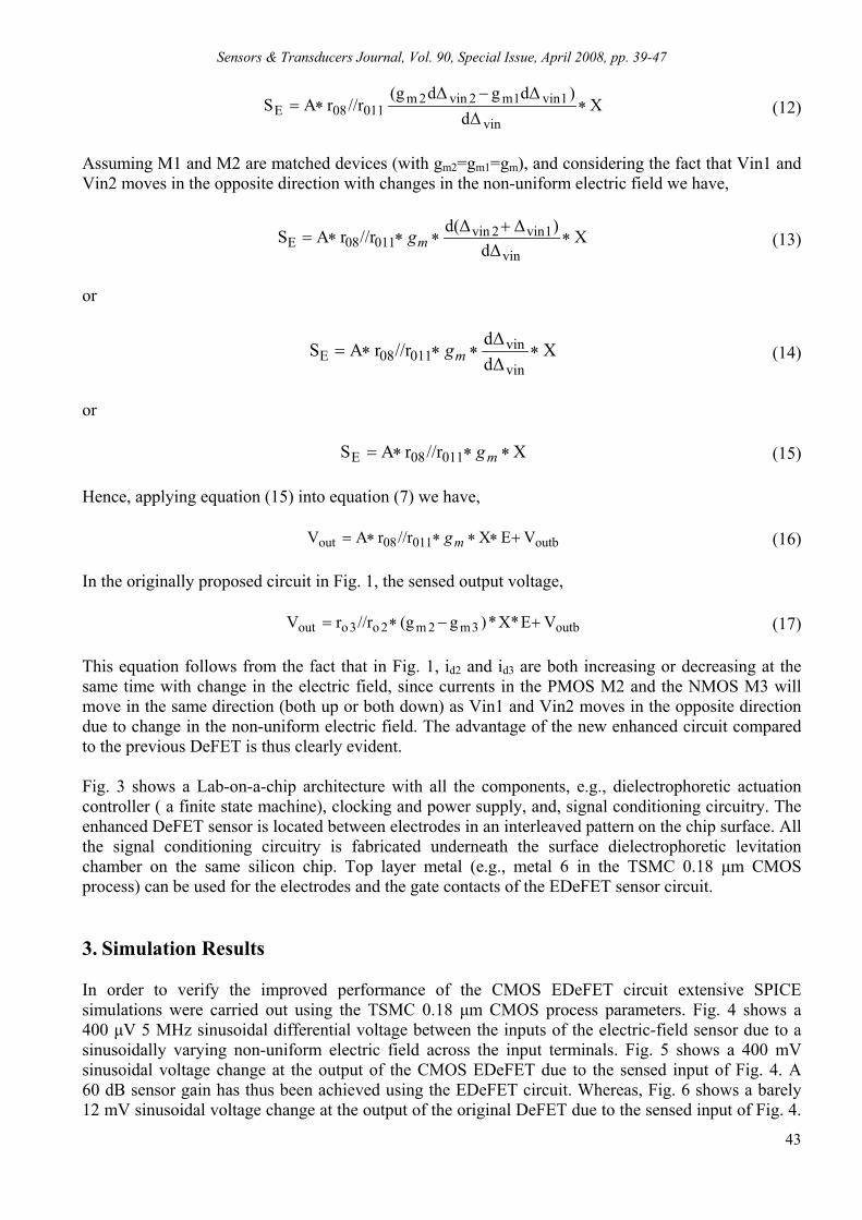
Sensors & Transducers Journal, Vol. 90, Special Issue, April 2008, pp. 39-47
43
X
d∆)d∆gd∆(g
//rrASvin
1vin1m2vin2m01108E ∗
−∗= (12)
Assuming M1 and M2 are matched devices (with gm2=gm1=gm), and considering the fact that Vin1 and Vin2 moves in the opposite direction with changes in the non-uniform electric field we have,
Xd∆
)∆d(∆//rrASvin
1vin2vin01108E ∗
+∗∗∗= mg (13)
or
Xd∆d∆//rrAS
vin
vin01108E ∗∗∗∗= mg (14)
or X//rrAS 01108E ∗∗∗= mg (15) Hence, applying equation (15) into equation (7) we have, outb01108out VEX//rrAV +∗∗∗∗= mg (16) In the originally proposed circuit in Fig. 1, the sensed output voltage, outb3m2m2o3oout VEX**)g(g//rrV +−∗= (17) This equation follows from the fact that in Fig. 1, id2 and id3 are both increasing or decreasing at the same time with change in the electric field, since currents in the PMOS M2 and the NMOS M3 will move in the same direction (both up or both down) as Vin1 and Vin2 moves in the opposite direction due to change in the non-uniform electric field. The advantage of the new enhanced circuit compared to the previous DeFET is thus clearly evident. Fig. 3 shows a Lab-on-a-chip architecture with all the components, e.g., dielectrophoretic actuation controller ( a finite state machine), clocking and power supply, and, signal conditioning circuitry. The enhanced DeFET sensor is located between electrodes in an interleaved pattern on the chip surface. All the signal conditioning circuitry is fabricated underneath the surface dielectrophoretic levitation chamber on the same silicon chip. Top layer metal (e.g., metal 6 in the TSMC 0.18 µm CMOS process) can be used for the electrodes and the gate contacts of the EDeFET sensor circuit. 3. Simulation Results In order to verify the improved performance of the CMOS EDeFET circuit extensive SPICE simulations were carried out using the TSMC 0.18 µm CMOS process parameters. Fig. 4 shows a 400 µV 5 MHz sinusoidal differential voltage between the inputs of the electric-field sensor due to a sinusoidally varying non-uniform electric field across the input terminals. Fig. 5 shows a 400 mV sinusoidal voltage change at the output of the CMOS EDeFET due to the sensed input of Fig. 4. A 60 dB sensor gain has thus been achieved using the EDeFET circuit. Whereas, Fig. 6 shows a barely 12 mV sinusoidal voltage change at the output of the original DeFET due to the sensed input of Fig. 4.

Sensors & Transducers Journal, Vol. 90, Special Issue, April 2008, pp. 39-47
44
This corresponds to a barely 30 dB sensor gain. The performance enhancement by the EDeFET circuit by way of around 30 dB higher sensitivity relative to DeFET circuit is thus clearly evident. Fig. 7 shows the gain bandwidth behavior of the EDeFET indicating a flat frequency response with around 58 dB gain until reaching a -3 dB frequency of around 10 MHz which ensures frequency-independent sensing over a wide range of time varying non-uniform electric field. Next, Fig. 8 shows an arbitrarily varying voltage difference (0-50 µV) between the sensor input devices due to arbitrary variations in an applied electric field. Finally, Fig. 9 shows the voltage change at the output of the CMOS EDeFET (0 – 110 mV) due to the sensed arbitrary input voltage change of Fig. 8. Again, in general a gain of over 60 dB is indicated by the EDeFET circuit.
Fig. 3. Lab-on-a-chip system showing all the components and the EDeFET located between electrodes.
Fig. 4. A 400 µV 5 MHz sinusoidally varying voltage difference between the sensor input devices due to sinusoidal variations in an applied electric field.

Sensors & Transducers Journal, Vol. 90, Special Issue, April 2008, pp. 39-47
45
Fig. 5. A 400 mV sinusoidal voltage change at the output of the CMOS EDeFET due to the sensed input of Fig. 4 (A 60 dB sensor gain).
Fig. 6. A 12 mV sinusoidal voltage change at the output of the original DeFET due to the sensed input of Fig. 4 (A 30 dB sensor gain achieved).
Fig. 7. A 10 MHz -3 dB bandwidth of the CMOS EDeFET circuit.
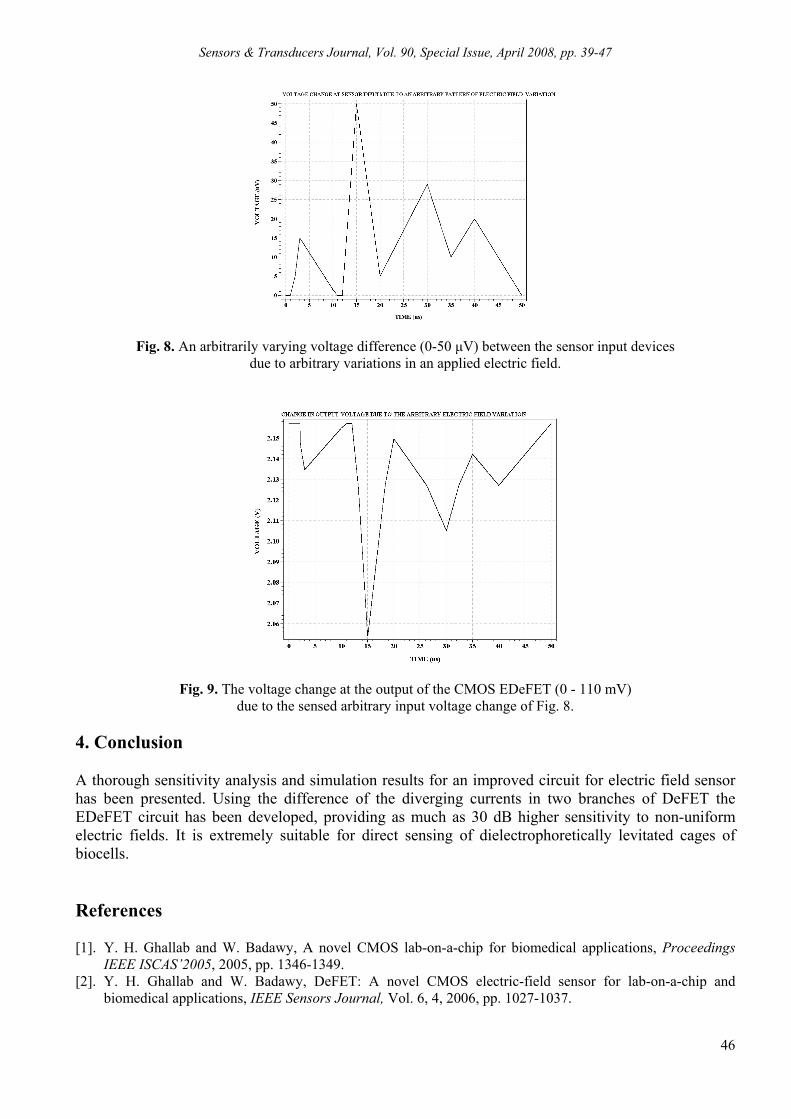
Sensors & Transducers Journal, Vol. 90, Special Issue, April 2008, pp. 39-47
46
Fig. 8. An arbitrarily varying voltage difference (0-50 µV) between the sensor input devices due to arbitrary variations in an applied electric field.
Fig. 9. The voltage change at the output of the CMOS EDeFET (0 - 110 mV) due to the sensed arbitrary input voltage change of Fig. 8.
4. Conclusion A thorough sensitivity analysis and simulation results for an improved circuit for electric field sensor has been presented. Using the difference of the diverging currents in two branches of DeFET the EDeFET circuit has been developed, providing as much as 30 dB higher sensitivity to non-uniform electric fields. It is extremely suitable for direct sensing of dielectrophoretically levitated cages of biocells. References [1]. Y. H. Ghallab and W. Badawy, A novel CMOS lab-on-a-chip for biomedical applications, Proceedings
IEEE ISCAS’2005, 2005, pp. 1346-1349. [2]. Y. H. Ghallab and W. Badawy, DeFET: A novel CMOS electric-field sensor for lab-on-a-chip and
biomedical applications, IEEE Sensors Journal, Vol. 6, 4, 2006, pp. 1027-1037.

Sensors & Transducers Journal, Vol. 90, Special Issue, April 2008, pp. 39-47
47
[3]. W. M. Arnold, Positioning and levitation media for the separation of biological cells, IEEE Transactions on Industry Applications, Vol. 37, 5, 2001, pp. 1468-1475.
[4]. Y. H. Ghallab and W. Badawy, Techniques for biocells sensing, detection and characterization, Proceedings 2005 International Conference on MEMS, NANO and Smart Systems, ICMENS’05, CD proceedings, 2005.
[5]. H. A. Pohl, Dielectrophoresis, Cambridge University Press, Cambridge, 1978. [6]. M. S. Talary and R. Pethig, Optical technique for measuring the positive and negative dielectrophoretic
behavior of cells and colloidal suspensions, Proceedings Inst. Elect. Eng. - Sci. Meas. Technol., Vol. 14, 5, 1994, pp. 395-399.
[7]. L. L. Sohn, O. A. Saleh, G. R. Facer, A. J. Beavis, R. S. Allan, and D. A. Notterman, Capacitance cytometry: measuring biological cells one by one, Proceedings Nat. Acad. Sciences, USA, Vol. 97, 20, 2000, pp. 10687-10690.
[8]. S. M. Rezaul Hasan and Siti Noorjannah Ibrahim, An enhanced CMOS electric field sensor circuit for cells sensing lab-on-a-chip application, Proceedings International conference on sensing technology(ICST), Palmerston North, 2007, pp. 255-259.
___________________
2008 Copyright ©, International Frequency Sensor Association (IFSA). All rights reserved. (http://www.sensorsportal.com)
Sensors & Transducers Journal, Vol. 90, Special Issue, April 2008, pp. 48-60
48
SSSeeennnsssooorrrsss &&& TTTrrraaannnsssddduuuccceeerrrsss
ISSN 1726-5479© 2008 by IFSA
http://www.sensorsportal.com
Coexistence of Wireless Sensor Networks in Factory Automation Scenarios
1Paolo FERRARI, 1Alessandra FLAMMINI, 1Daniele MARIOLI,
1Emiliano SISINNI, 2Andrea TARONI 1Department of Electronics for Automations, University of Brescia, Brescia, Italy
Tel.: +39 030 3715445 E-mail: [email protected]
2Carlo Cattaneo University, Castellanza, Italy Tel. +390331572214
E-mail: [email protected]
Received: 15 October 2007 /Accepted: 20 February 2008 /Published: 15 April 2008 Abstract: The factory automation world can take advantage from innovative wireless sensors network applications, but installation of several wireless systems in the same industrial plant will raise coexistence problems. However, in general, industrial Wireless Sensor Networks (WSNs) operate cyclically and coexistence can be obtained exploiting this characteristic. The paper proposes a methodology based on a central arbiter that assigns medium resources according to requests coming from WSN coordinators. An infrastructure (e.g. a wired Real-Time Ethernet (RTE) network) assures synchronization and distribute resource allocation results. A simulation framework has been designed to evaluate allocation scheme and WSNs coexistence before physical implementation. The real feasibility of the proposed approach has been demonstrated by means of prototype WSNs (based on IEEE802.15.4) synchronized by means of PROFINET IO RT_Class 3 network. Experimental results show a synchronization accuracy below 4 µs that allows reading of two WSNs (32 nodes) in 128 ms without collisions. Copyright © 2008 IFSA. Keywords: Wireless sensor, Wireless network, Synchronization, Factory automation 1. Introduction Wireless sensor networks (WSNs) are not diffused in industry, yet. Nowadays, their most diffused application for factory automation is the so called “cable replacement”, where wireless links are used

Sensors & Transducers Journal, Vol. 90, Special Issue, April 2008, pp. 48-60
49
for bridging two wired fieldbus segments. For instance, wireless communication is employed to replace brush-contacts in rotating machine. Up to now, a relatively small number of products are available for industrial of applications. Generally, WSNs are employed for monitoring and not for control, since they still have reliability problems. In fact, radio transmission is subjected to a higher Bit Error Rate (BER) than cable transmission, especially if transmission power is low (in order to preserve battery charge) and interference is heavy (as on industrial sites). Moreover, most of the wireless technologies in use today have been developed without any kind of cooperation between their promoters. This means that, in general, wireless standards are not only incompatible, but also “competing”. They share the same media and, in many cases, also the same frequency bandwidth (ISM, Industrial Scientific and Medical). A new standard must adopt some “surviving” strategies in order to share the medium with an older standard [1]. As an example, spread spectrum modulation techniques like Frequency Hopping (FHSS) and Direct Sequence (DSSS) have been adopted to minimize interferences. This approach, that considers interfering communications as mere noise sources, is effective, since these systems can operate without caring about other “things” emitting in the same area. However, there are some drawbacks. First of all, “surviving” does not mean “working at best”; actions like retransmissions, frequency change, etc. etc. require a lot of overhead reducing efficiency (energy waste!). Secondly, the available medium is misused, reducing the number of nodes (i.e. sensing elements) that can be effectively utilized in the same area. In our opinion, the key feature that must be stressed to ensure the highest efficiency is coexistence. It stands for the ability of wireless systems to slightly modify their behaviour in order to eliminate any mutual interference. In other words, two WSNs in the same area can change, accordingly, their media access strategies to avoid collisions (in the time and frequency domains). Clearly, the behavioral change is possible because the involved systems have knowledge about other co-located wireless devices. In [2] system architecture to synchronize WSNs by means of synchronization services offered by Real-Time Ethernet protocols has been proposed. Factory automation is the application area for the proposed solution, and in this field the use of Ethernet as fieldbus is well accepted. Recently, new RTE protocols (like PROFINET, Ethernet/IP, EtherCAT, TCnet, Vnet/IP, etc.) have been standardized by IEC FDIS 61784-2. Some of them offer synchronization accuracy among nodes well below 1 µs, a good value for the proposed use. In this paper we suggest that coexistence of wireless-equipped machines must be reached with a minimum exchange of information among systems and with no alteration of the machine characteristics. Particularly, the synchronization among WSNs is a good basis on which the coexistence among different types of network can be build. The idea is to have a central arbiter that knows the requirements of all the WSNs; it allocates medium access rights to WSN coordinators that can apply these rules safely because they are synchronized by means of an RTE network. The paper introduces wireless sensing in automation in Section 2 and presents some conclusions on coexistence of the most diffused wireless protocol in Section 3. The proposed architecture and the associated simulation framework are illustrated in Section 4. The experimental tests are in Section 5. 2. Factory Automation and Wireless Sensors A current scenario of industrial automation is composed of several tool machines from different manufacturers working close together in the same area (the industrial plant). A typical example is shown in Fig. 1, where a machine prepares the work pallets which are fed to several adjacent
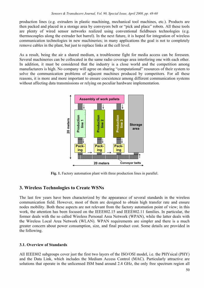
Sensors & Transducers Journal, Vol. 90, Special Issue, April 2008, pp. 48-60
50
production lines (e.g. extruders in plastic machining, mechanical tool machines, etc.). Products are then packed and placed in a storage area by conveyors belt or “pick and place” robots. All these tools are plenty of wired sensor networks realized using conventional fieldbuses technologies (e.g. thermocouples along the extruder hot barrel). In the next future, it is hoped for integration of wireless communication technologies in new machineries; in many applications the goal is not to completely remove cables in the plant, but just to replace links at the cell level. As a result, being the air a shared medium, a troublesome fight for media access can be foreseen. Several machineries can be collocated in the same radio coverage area interfering one with each other. In addition, it must be considered that the industry is a close world and the competition among manufacturers is high. No company will agree on sharing “computational” resources of their system to solve the communication problems of adjacent machines produced by competitors. For all these reasons, it is more and more important to ensure coexistence among different communication systems without affecting data transmissions or relying on peculiar hardware implementation.
Assembly of work pallets
Pack-ing
20 meters
Pack-ing
Storagearea
Prod
uctio
n
line
1 (
hit
l)
Conveyor belts
20 m
eter
s
Pack-ing
Prod
uctio
n
line
2
Prod
uctio
n
line
3
Fig. 1. Factory automation plant with three production lines in parallel. 3. Wireless Technologies to Create WSNs The last few years have been characterized by the appearance of several standards in the wireless communication field. However, most of them are designed to obtain high transfer rate and ensure nodes mobility. Both these aspects are not relevant from the factory automation point of view; in this work, the attention has been focused on the IEEE802.15 and IEEE802.11 families. In particular, the former deals with the so called Wireless Personal Area Network (WPAN), while the latter deals with the Wireless Local Area Network (WLAN). WPAN requirements are simpler and there is a much greater concern about power consumption, size, and final product cost. Some details are provided in the following. 3.1. Overview of Standards All IEEE802 subgroups cover just the first two layers of the ISO/OSI model, i.e. the PHYsical (PHY) and the Data Link, which includes the Medium Access Control (MAC). Particularly attractive are solutions that operate in the unlicensed ISM band around 2.4 GHz, the only free spectrum region all

Sensors & Transducers Journal, Vol. 90, Special Issue, April 2008, pp. 48-60
51
around the world. Lower frequencies could have a lower attenuation, but the better behaviour in terms of electromagnetic interference and frequency reuse makes ISM the best choice. The previously mentioned WPAN is defined around the concept of Personal Operating Space (POS), i.e. “the space about a person that typically extends up to 10 meters in all directions and envelops the person whether stationary or in motion”; a concept that can be easily applied also to machineries. IEEE802.15 is composed of four working groups. Only two of them will be discussed. IEEE802.15.1 is the standard version of the Bluetooth solution. It employs a narrowband radio and implements spreading by means of FHSS over 79 (1-MHz wide) channels. A scheduled MAC is adopted, since time is divided into 625µs-slots alternatively assigned to network master and slaves. The same physical channel is shared within the so called piconet that can include up to 8 active members; if a node exists in more than one piconet it belongs to a scatternet. The gross transfer rate is 1Mbps. IEEE802.15.4 emphasizes low power consumption; it allows for a gross transfer rate of up to 250 Kbps. The spreading technique is the DSSS and the available band is divided into 16 channels 5-MHz wide. Both star and peer-to-peer topologies are supported and the MAC technique is based on carrier sensing, even if it is possible to allocate particular time slots to nodes with restrictive time requirements. Two kinds of nodes are defined: Full Functionalities Device (FFD), that implements the whole stack and require more resources, and Reduced Functionalities Device (RFD), that implements a subset and can be easily implemented on low cost hardware. On the contrary, IEEE802.11 has been designed to replace Ethernet connection and offers transmission rate comparable with the 10/100BaseT wired link. Power consumption is not of main concern and usually the implemented network is infrastructured, i.e. it relies on several “Access Points” interconnected by a wired backbone that manages wireless nodes. However, “ad hoc” implementations are also described. The 802.11b version employs DSSS with a gross transfer rate of up to 11 Mbps, while 802.11g employs OFDM with a gross transfer rate of 54 Mbps. Both of them define 14 channels in the 2.4 GHz band, each having a distance of 5 MHz. Since the WLAN radio signal has a bandwidth of 22 MHz, not all channels can be used concurrently, but there is room only for three non-overlapping channels: 1, 7 and 13 (in Europe). The MAC strategy is based on carrier sensing, but some form of time scheduling and priority services is provided. 3.2 Interoperability and Coexistence Different systems that work using the same set of rules are said to be interoperable; on the contrary, coexistence is the capability to work in an environment where other devices can operate following dissimilar rules. As previously stated, each manufacturer generally considers other communication systems as noise sources. Some efforts have been done to overcome this approach and to give indications on how ensure coexistence. Task Group IEEE 802.15.2 (TG2) was formed in 2000 to address issue of coexistence of WLAN and WPAN, primarily 802.11b and 802.15.1 (i.e. Bluetooth). However, it must be remembered that now IEEE802.15.2 is in hibernation; its suggestions have only partially been included in IEEE802.11 and IEEE802.15 standards. TG2 defines two different approaches: collaborative and non-collaborative. In the former, systems exchange information and thus are linked together, while in the latter each one guesses the existence of other systems analyzing the medium itself. Best results may be obtained with collaborative mechanisms, i.e. exploiting all information available on fighting communication systems [3]. The simplest collaborative method is the so called “Alternating Wireless Medium Access” (AWMA). The basic idea is to coordinate the medium access so that no collision occurs at all. This implies that both the WLAN and the WPAN coordinators are linked together and synchronized; the WLAN node

Sensors & Transducers Journal, Vol. 90, Special Issue, April 2008, pp. 48-60
52
schedules network accesses defining a “Medium free signal” that is used to notify the WPAN interval. The WLAN Beacon packet is modified in order to add a MSE (Medium Sharing Element) field that specifies intervals time duration. Particularly interesting is the “Packet Traffic Arbitration” (PTA), where an additional arbiter uses knowledge of networks status, packet priorities and PHY characteristics to deny transmission of packets that may result in collisions. The last collaborative method is the “Deterministic Interference Suppression” (DIS); this approach can be used when one of the communication systems can be considered as a narrow band interfering signal, as occur in WLAN transmissions with respect to IEEE802.15.1. This kind of interfering signal can be filtered out knowing its time and frequency behaviour in the receiving demodulator, thus improving robustness. Non-collaborative methods must be employed when a-priori knowledge is not available and they are useful when dealing with changing data streaming. There is also the IEEEP802.19 Wireless Coexistence Technical Advisory Group, formed in 2001 to address wireless coexistence across all of IEEE 802. The aim is to develop a document called Coexistence Assurance (CA) document, which is a study showing how well a proposed wireless standard, planned for unlicensed operation, coexists with current standards. Anyway, it is still in a draft state. 3.3. The Industrial Scenario In the literature, several proposals have been done in order to improve coexistence of wireless systems for the consumer market (especially for IEEE802.15.1 and IEEE802.11b [4, 5]). In this case problems may arise when both radios are co-located within the same device, e.g. a laptop. The considered scenario involves bursty and asynchronous transmissions of a relatively high amount of data. Usually, latency is not of main concern and suggested solutions implement data queuing and postponed data transmission. The industrial scenario is just the opposite; the data delivery model involves cyclic data transmission (to ensure determinism) of a relatively small data amount at a low transfer rate. In fact, first available wireless sensing solutions for the factory automation [6] adopt star topology with Time Division Multiple Access (TDMA) strategy. Non-collaborative approaches are preferred in the home/office environment, since scalability and self healing are key features in consumer applications. Again, the industrial scenario has completely different requirements; wired links are always present and best results can be reached recurring to collaborative schemes. 4. The Proposed Architecture As previously stated, in industrial applications it is very difficult to ensure coexistence relying on collaboration between systems of different manufacturers. On the other hand, all vendors propose wireless solutions that do not constantly occupy the entire free spectrum. This means that sometimes a system has to leave the bandwidth free of traffic. Synchronization of network coordinators can help in exploiting such “fairness” characteristics in order to allow for coexistence among networks even from different vendors. The proposed solution (Fig. 2) is a sort of arbiter that harmonizes medium accesses by means of time reference sharing and global knowledge of the whole plant. The arbiter does not care about application data transmitted on the networks, it just exchanges some configuration information to quantify requirements of each network. In particular, the arbiter creates a map of time, frequency, geographical area requests of every network. Successively, it “orthogonalizes” these specifications in order to avoid or decrease mutual interference.

Sensors & Transducers Journal, Vol. 90, Special Issue, April 2008, pp. 48-60
53
Range of WSN y
RTE backbone
WSN x Coordinator
WSN y Coordinator
WSN z Coordinator
MetaMAC(Arbiter)
Range of WSN y
Range of WSN z
Range of WSN y
RTE backbone
WSN x Coordinator
WSN y Coordinator
WSN z Coordinator
MetaMAC(Arbiter)
Range of WSN y
Range of WSN z
Fig. 2. The proposed system. The proposed arbiter works at the MAC level, since strategies at the PHY level implies hardware modifications which are not tolerated. For this reason the proposed arbiter has been called “MetaMAC”. Rather than organize all the nodes collocated in the same area of interest, the MetaMAC only talks with WSN coordinators that continue to manage their subnets on their own. This allows for a simpler solution with a lower impact on existing solutions. WSN coordinators are usually connected by means of fieldbuses or RTE networks and MetaMAC could also use this infrastructure. Since in new installations RTE is preferred, the exchange of configuration and synchronization data can rely on RTE performance. The previously introduced map should also be flanked by ancillary information, such as channel/link quality (RSSI, PER, BER…), retry strategies (Automatic Repeat Request - ARQ, number of retries…), etc. Using this knowledge the MetaMAC can more effectively apply safety strategies. In this scenario frequency hopping or ARQ should be performed under the MetaMAC supervision. For instance, it could be preferable to disable retransmission to ensure several TDMA networks coexistence. 4.1 Simulation Framework A simulation framework has been created, in order to test the architecture behavior with arbitrary networks and protocols. OMNeT++ has been used as simulation environment: models of wireless nodes as well as models of resource allocators can be implemented as C++ objects that exchange messages. Each node has its own properties like position, transmission power, sensitivity, protocol, and internal state machine. The compound module representing a WSN is shown in Fig. 3: several nodes are collected together representing a wireless network. At least one coordinator is present in every WSN and each coordinator has a double data path (wired and wireless), so it can send (or receive) information along a wired connection in a sort of double tier network. The model of the MetaMAC has been created and it can be interfaced with other coordinators by means of the wired network. A snapshot of the simulator appearance at the highest level of abstraction is shown in Fig. 4.

Sensors & Transducers Journal, Vol. 90, Special Issue, April 2008, pp. 48-60
54
Fig. 3. Simulation module representing a WSN.
Fig. 4. Simple coexistence simulation: two WSNs are coordinated by a MetaMAC. Both networks receive medium access rights via the RTE_backbone and try to access the wireless channel accordingly.
It should be noted the presence of another compound module (the “cloud”) that models the wireless channel behavior; in fact wireless nodes exchange message passing through the wireless channel model in order to simulate the shared nature of the medium. The wireless channel model takes into account the presence of a finite number of radio channels, the attenuation and the fading due to physical node position (i.e. the x and y coordinates), the noise, the collisions when two nodes attempt transmitting at the same time/on the same frequency. The framework is versatile, since no assumptions has been done on the nature of the wireless network or the wired network; the scenario can be customized by the user before starting the simulation.
Sensors & Transducers Journal, Vol. 90, Special Issue, April 2008, pp. 48-60
55
5. Example of a Real Application The simulation scenario described in the previous section has been tested on a real application. A plastic machining plant, where two extruders are flanked one each other, has been considered. The fluid temperature is continuously measured by means of wireless thermocouples [7]; each extruder has its own star network with up to 16 nodes operating with an hybrid CSMA/TDMA strategy and exploiting a PHY level compliant with IEEE802.15.4. A wireless thermocouple prototype is shown in Fig. 5.
Wireless thermocouple
Power supply board
CPU+RF
Power supply board
CPU+RF
AmpAmpADCADC CPUCPU Tx/Rx
MC13192Tx/Rx
MC13192
Power Supply2AA+TPS61016Power Supply
2AA+TPS61016
MUX
MUX
TCJ
LM60HCS08GT60
XBee
Fig. 5. Photo and block diagram of a wireless thermocouple prototype. Usually, in order to assure coexistence of multiple WSNs and to increase the number of sensors, different frequency channels are chosen. With the aim of implementing a prototype of two interfering WSNs, authors considered two systems operating on the same channel. The wireless protocol of both WSNs is very simple; each network coordinator divides time into segments by means of particular packets called Beacons. The portion that immediately follows a Beacon (JP, Join Period) is used for acyclic communications and uses CSMA/CA. Once a node has joined its coordinator, it receives a communication time slot and performs cyclic data exchange on TDMA basis in the remaining portion of the frame (RTP, Real-Time Period). Obviously, if more than one network operates on the same channel and covers the same area collisions may arise as in Fig. 6. For instance, Beacon overlap condition can last for several seconds, while the offset between time segments of the two WSNs shifts (randomly) for thermal drift. The considered protocol has two kinds of packet: Beacon and Data. No ACK packets are provided since data exchange is continuous and cyclic (i.e. retries are useless). The Beacon packet is 13 bytes long (416 µs @ 250 Kbps) including IEEE 802.15.4 header and footer. The Data packet is 18 bytes long (576µs @ 250kbps). In the current implementation, the segment is 128 ms wide: JP lasts 32 ms and RTP lasts 96 ms (16 time slots of 6 ms). However, each time slot is occupied for just the duration of a Data packet in air. The proposed MetaMAC has been used to opportunely shift frames of both networks in order to avoid collisions (see Fig. 7). The offset accuracy between Beacons of the two WSNs depends on RTE synchronization accuracy. On the other hand, the relative position of time slots depends on the WSN synchronization accuracy.
Sensors & Transducers Journal, Vol. 90, Special Issue, April 2008, pp. 48-60
56
Data exchange of sensorsBeacon
Time
Time WSN time segment
Collision
WSN 2
WSN 1
JP RTP
Fig. 6. Two unsynchronized WSNs with collisions.
Time
Constant offset between beacon
Time
Constant offset between timeslots
WSN 2
WSN 1
Fig. 7. The MetaMAC decides the offset between WSN time segments, avoiding collisions. The realized prototype system is shown in Fig. 8. RTE Node 1 includes also the MetaMAC functionalities, since it has a high performance microprocessor. A total of 32 wireless sensors (16 sensors for each coordinator) are present in the system.
Sync
RTE backbone (PROFINET IO)
Wirelesssensors
Node 1
WSN 1 coordinator
Data Node 2
WSN 2 coordinator
MetaMAC(Arbiter)
Sync
RTE backbone (PROFINET IO)
Wirelesssensors
Node 1
WSN 1 coordinator
Data Node 2
WSN 2 coordinator
MetaMAC(Arbiter)
MetaMAC(Arbiter)
Fig. 8. Block diagram of the prototype system.

Sensors & Transducers Journal, Vol. 90, Special Issue, April 2008, pp. 48-60
57
5.1. RTE Network In the prototype system, PROFINET IO RT_Class_3 has been used as RTE protocol. PROFINET IO RT_Class 2 and 3 cover the CP 3/6 of the new international standard IEC FDIS 61784-2. A good introduction to PROFINET IO is presented in [8]. Briefly, PROFINET IO defines IO-Controllers (i.e. intelligent devices which carry out automation tasks) and IO-Devices (i.e. field devices like sensors, actuators, IO module etc.). IO-Controllers and IO-Devices exchange process data using real-time communication channels; for configuration, statistics, and management data non real-time channels (i.e. UDP/IP) are used. PROFINET IO grade of determinism is described with the class number: RT_Class 2 and RT_Class 3 (often called IRT, Isochronous Real-Time) are used with applications requiring isochrony and cycle time in the order of 1 ms. In particular, RT_Class 3 (also called IRTtop) is the top performance class. No delays can happen within this RT_Class since the frame scheduling sequence in each cycle is “a priori” known and always identical. The network configuration tool calculates the trip for every frame of a cycle and downloads the schedule in the RTE network infrastructure (i.e. RT_Class 3 compliant switches). In [9], performance of a PROFINET RT_Class 3 system has been experimentally evaluated. At the network level the synchronization accuracy is below 150 ns. At the application layer interface, results indicate that maximum offset errors between real nodes of an RT_Class 3 system is less than 3 µs with a standard deviation of 500 ns. Moreover, the performance could be improved in the future with simple firmware modifications. In this paper the PROFINET IO network is composed of an IO-Controller (Node 1) and an IO-Device (Node 2). Both of them are based on ERTEC400 ASIC (Siemens) which includes an ARM9 core, running WxVorks operating system, and Ethernet interfaces. 5.2. WSN Two kinds of wireless coordinator have been realized, as illustrated in Fig. 8. The first one is obtained joining the IOC 1 node, described in previous section, with a traditional dual chip (a microcontroller, HCS08GT60 and a transceiver, MC13192, both from Freescale) coordinator. The Node 1 furnishes a synchronization signal that is used by the network coordinator to mark Beacon transmission instants. In the other coordinator the same processor of the Node 2 handles both wireless and PROFINET protocols. The only other component is the radio frequency transceiver (MC13192). Wireless nodes are based on the same hardware (µC: HCS08GT60, transceiver: MC13192; see Fig. 5) and are battery powered; a DC/DC converter (TPS60016 from TI) has been adopted to obtain power supply from two AA batteries; life has been estimated in about 4 months of continuous working. The sensing element is a common J-type thermocouple whose conditioning chain has been designed around a low-power low-noise amplifier (OPA330 from TI). The overall accuracy is in the order of 1°C and resolution is 0.1°C. 6. Experimental Results WSN coordinators are always on and remain in the transmitting state only to send Beacons, otherwise they listen to what happens on air. On the contrary, wireless sensors use low power modality in order to extend their life. They spent most of their time turned off (Doze mode of the MC13192); wakeup instants are determined using the high accuracy crystal based timer (resolution 1 µs).

Sensors & Transducers Journal, Vol. 90, Special Issue, April 2008, pp. 48-60
58
In order to precisely determine time position of packet in air, a purposely designed sniffer has been realized. It uses a different transceiver compliant with the IEEE802.15.4 (CC2420 from TI), which offers a digital line that signals the arrival time of each packet and its duration. The signal goes high after the packet Start Frame Delimiter has been detected and goes low at the packet end. Therefore, the signal pulse durations are 256 µs for the Beacon and 416 µs for the Data, since the 4-bytes preamble and the 1-byte SFD fields are not included. Referring to Fig. 9, a mixed signal scope (MSO6054A from Agilent) has been used to simultaneously show: the packet duration signal given by the sniffer (AIRPKT trace); the transmission and reception signals from the MAC layers of WSN coordinators (traces CRD1 and CRD2) and nodes (the traces NODES1 and NODES2 are the OR combination of all the node signals). The synchronization pulse sent by IOC 1 (trace SYNC) is also displayed. The proposed MetaMAC decides to separate the begin of WSN 1 and WSN 2 cycle of 2 ms, achieving coexistence of the two networks. The synchronization through the PROFINET IO network allows the exact positioning of Beacons. As a result, the system correctly manages 32 co-located wireless sensors in a time segment of 128 ms, harmonizing their operations on the same frequency channel. Fig. 10 is a detail of the end of time segment n and the begin of time segment n+1. Data packets coming from the 16th sensor of WSN 1 and WSN 2 are visible, together with the Beacons of the new time segment. In the two boxes are shown, by means of oscilloscope persistence, the magnification of the transmission instant of: the 16th sensor; the Beacon of WSN 2. The offset accuracy, measured over 15 minutes, is very good; the jitter (the maximum offset minus the minimum offset) is 3.5 µs for Beacons and 5.5 µs for sensors. It should be remarked that the last wireless node has the largest time inaccuracy because it remains in the doze mode for the longest time after receiving a Beacon.
Segment n n + 1n - 1
Packets in the air
802.15.4 packet sniffer
Sync reference distributed by RTE network
Tx/Rx interrupts in nodes of WSN 1
Tx/Rx interrupts in nodes of WSN 2
Worst case
Segment n n + 1n - 1
Packets in the air
Segment n n + 1n - 1
Packets in the air
802.15.4 packet sniffer
Sync reference distributed by RTE network
Tx/Rx interrupts in nodes of WSN 1
Tx/Rx interrupts in nodes of WSN 2
Worst case
Worst case
Fig. 9. A complete time segment (128 ms) of the real system. AIRPKT: signal given by the network sniffer indicating the position of packets in the air.

Sensors & Transducers Journal, Vol. 90, Special Issue, April 2008, pp. 48-60
59
16th sensorof WSN 1
Beacon of WSN 1
Beaconof WSN 2
5.5 µs 3.5 µs
16th sensorof WSN 2
Sensor jitter Beacon jitter
Fig. 10. Last part of a time segment and Beacons of the next segment. In the boxes: jitter of the 16th sensor of
WSN 2 and jitter of WSN 2 Beacon. 7. Conclusion In this paper, a methodology based on an arbiter for coexistence of different WSNs has been proposed. Resources harmonization is obtained by means of a common sense of time among WSN coordinators; synchronization is done using a wired Real-time Ethernet network. A simulation framework has been also provided in order to test resource allocation strategies with different WSN protocols. Last, the applicability of the architecture has been demonstrated by means of a prototype system that can interleaved time scheduling of two WSNs (operating on the same frequency channel) with an error less than 10 µs. In conclusion, the proposed architecture and the related simulation tool give the possibility to test coexistence among generic WSNs (e.g. Bluetooth and IEEE802.15.4 Zigbee) before the physical placement of the networks. References [1]. A. Willig, K. Matheus, A. Wolisz, Wireless technology in industrial networks, Proc. of the IEEE, Vol. 93,
Issue 6, June 2005, pp. 1130-1151. [2]. P. Ferrari, A. Flammini, D. Marioli, E. Sisinni, A. Taroni, Coexistence of Different Wireless Sensor
Networks exploiting Real-Time Ethernet synchronization, Proc. of ICST2007, 4-7 June 2007, pp. 1916-1920.
[3]. C. F. Chiasserini, R. R. Rao, A comparison between collaborative and non-collaborative coexistence mechanisms for interference mitigation in ISM bands, Proc. of VTC2001, Vol. 3, 6-9 May 2001, pp. 2187-2191.
[4]. M. C. Chek, Y. Kwok, Design and evaluation of practical coexistence management schemes for Bluetooth and IEEE 802.11b systems, Computer Networks, Vol. 51, Issue: 8, June 2007, pp. 2086-2103.
[5]. A. Nallanathan, W. Feng, H. K. Garg, Coexistence of wireless LANs and Bluetooth networks in mutual interference environment: An integrated analysis, Computer Communications, Vol. 30, Issue. 1, December 2006, pp. 192-201.
[6]. D. Dzung, C. Apneseth, J. Endresen, J. E. Frey, Design and implementation of a real-time wireless sensor/actuator communication system, Proc. of ETFA 2005, Vol. 2, Sept. 2005, pp. 19-22.
[7]. A. Flammini, D. Marioli, E. Sisinni, A. Taroni, A real-time wireless sensor network for temperature

Sensors & Transducers Journal, Vol. 90, Special Issue, April 2008, pp. 48-60
60
monitoring, Proc. of ISIE 2007, 4-7 June 2007, pp. 1916-1920. [8]. M. Popp, K. Webber, The rapid way to PROFINET, PROFIBUS Nutzerorganization e.V., 2004. [9]. P. Ferrari, A. Flammini, D. Marioli, A. Taroni, F. Venturini, Evaluation of timing characteristics of a
prototype system based on PROFINET IO RT_Class 3, Accepted for ETFA 07, 25-28 September 2007, Patras (Greece).
___________________
2008 Copyright ©, International Frequency Sensor Association (IFSA). All rights reserved. (http://www.sensorsportal.com)
Sensors & Transducers Journal, Vol. 90, Special Issue, April 2008, pp. 61-71
61
SSSeeennnsssooorrrsss &&& TTTrrraaannnsssddduuuccceeerrrsss
ISSN 1726-5479© 2008 by IFSA
http://www.sensorsportal.com
Wireless Passive Strain Sensor Based on Surface Acoustic Wave Devices
T. Nomura, K. Kawasaki and A. Saitoh
Faculty of Engineering Shibaura Institute of Technology, Tokyo, Japan
E-mail: [email protected]
Received: 15 October 2007 /Accepted: 20 February 2008 /Published: 15 April 2008 Abstract: Surface acoustic wave (SAW) devices offer many attractive features for applications as chemical and physical sensors. In this paper, a novel SAW strain sensor that employs SAW delay lines has been designed. Two crossed delay lines were used to measure the two-dimensional strain. A wireless sensing system is also proposed for effective operation of the strain sensor. In addition, an electronic system for accurately measuring the phase characteristics of the signal wave from the passive strain sensor is proposed. Copyright © 2008 IFSA. Keywords: Surface acoustic waves, SAW sensor, Strain sensor, Wireless sensing, SAW delay line 1. Introduction Today, many different fields require measurement of strain and its distribution. Particularly notable today is the need for health and safety monitoring for the sake of safety and comfort, which requires constant monitoring of strains within complex structures and buildings as well as the strain distributions in mobile objects, typically the wings of an aircraft [1]. The traditional way to measure strain is using a resistance strain gauge, which is mainly structured to measure unidirectional strains. However, as is the case when measuring stress, rosette analysis is required when measuring strains on a plane. Rosette analysis requires multiple elements to be positioned together at a single location and used simultaneously. Consequently there a large number of elements and accordingly a large number of electrical supply lines, making the measurement process very complex.

Sensors & Transducers Journal, Vol. 90, Special Issue, April 2008, pp. 61-71
62
A surface acoustic wave (SAW) can be easily excited on a piezoelectric substrate using an interdigital transducer (IDT). Most of such a wave’s energy is concentrated within a depth of a single wavelength from the substrate’s surface. Its propagation characteristics are easily affected by external physical and electrical changes. This is why applications of SAW’s include sensors for measuring physical parameters. Recently, there have been many reports on SAW sensors that take advantage of SAW’s propagation characteristics, which change easily in response to external factors [2], [3], [4], [5]. One advantage of using SAWs in sensors is that, since SAWs are slower than electromagnetic waves by approximately five orders of magnitude, these sensors can be made more compact. Furthermore, increasing the frequency of the sensors improve their precision and resolution. In this paper, we clarify the relationship between changes in the propagation path length of a SAW and the phase of the wave. We then discuss a strain sensor that utilizes changes in the speed of a SAW caused by strain in the SAW device. Although some reports on sensors using SAWs have been published, they mostly discussed one-dimensional strains [6], [7]. However in this study, we developed a SAW strain sensor that simultaneously measures strains in two directions using two SAW delay lines that intersect each other perpendicularly on a single substrate. As demonstrated in the experiment reported below, we herein propose a two-dimensional strain sensor that simultaneously measures strains in two different directions using two delay lines that cross each other at right angles. These two delay lines exist on an anisotropic piezoelectric substrate (128° Y-cut, X-propagating LiNbO3). As its working principle, this strain sensor monitors changes in the propagation path length caused by strains applied to the piezoelectric substrate. Furthermore, in this study we show that when this new SAW strain sensor is connected directly to an antenna it is capable of passive remote sensing. 2. Measurement of Strain Using SAW In this section, the principle and the method of measurement of strain using SAW delay line is described. 2.1. Principle of Measurement When a strain is applied to a substrate containing a SAW delay line, the propagation path length changes (see Figs. 1(a) and (b)). Let this change in propagation path length be denoted by ∆l, and we then obtain the following expression for ∆θ, the phase difference between the input and output waves: ( )
( )vl
vl
vllv
ll
∆±=−
∆±=∆
∆±=∆+
ωωωθ
ωθθ (1)
l: Propagation distance (m), ν: Propagation velocity (m/s), θ: Phase difference (rad.), ω: frequency (rad. /s), Therefore, by measuring the amount of phase change between the input and output of a delay line caused by a strain, we can determine the magnitude of the strain.

Sensors & Transducers Journal, Vol. 90, Special Issue, April 2008, pp. 61-71
63
This magnitude of the strain can be calculated using Eqn. (1), using the amount of change caused by the strain, with reference to the phase difference when no strain is applied.
(a) Overview of SAW delay line and strain.
(b) Side view of an SAW delay line.
Fig. 1. Schematic diagram of strain sensor using SAW delay line. 2.2. Measurement System of Phase Change For a SAW strain sensor to function correctly, changes in the phase of the SAW must be accurately measured. In the following, we briefly describe the circuit that was used to accurately measure the phase in our measurements. Fig. 2 shows the measuring circuit that we used in the experiment to precisely measure phase changes produced by strain. The standard signal generator (SSG) generates a continuous wave that is then divided into two by the power divider. One component is used as a reference wave and the other is used for measuring. This measurement component of the continuous wave is input into the mixer together with a rectangular wave from a pulse function generator (pulse FG). This produces a tone burst wave, which is used to excite the SAW device. If the device is strained, the propagation length changes, and a phase difference that corresponds to the strain is produced. An automatic gain control amplifier (Amp.1 and Amp.2) is used to amplify the continuous wave divided for a reference and the tone burst wave in which a phase difference has been produced due to propagation through the SAW device, so that these two waves have equal amplitudes. If the continuous wave used as a reference and the tone burst wave with the phase difference are input into the mixer, the mixer outputs a signal that corresponds to the phase difference between the two waves. This phase difference signal from the mixer is used as the output signal.
S.S.G
PulseF.G.
Attenuator
SAW device
L.P.Filter
PowerDivider
Mixer
Out
Amp.1
Amp.2
Fig. 2. Schematic diagram of strain sensor system.
IDT IDT
t

Sensors & Transducers Journal, Vol. 90, Special Issue, April 2008, pp. 61-71
64
3. Strain Sensor Using SAW Devices We first clarify the characteristics of a one-dimensional strain sensor with a delay line, in order to understand the basic characteristics of a SAW strain sensor. 3.1. One-dimensional Strain Sensor Fig. 3 shows a SAW sensor that measures unidirectional strains. This sensor has a pair of IDTs, one for receiving and the other for transmitting, fabricated on its piezoelectric substrate, as shown in Fig. 1(a). It measures strains in a single direction only, and is composed of a single-channel delay line. We constructed a strain sensor with a one-dimensional delay line on a 128° Y-cut, X-propagating LiNbO3 substrate, and examined its characteristics. The sensor was composed of a delay line with a propagation path length of 100 λ (λ: wavelength) and a frequency of 40 MHz.
GND
OUTINx
y
Fig. 3. One-dimensional strain sensor pattern. 3.2. Measurement Method In the experiments, we attached the SAW strain sensor to a 10 cm × 10 cm phosphor bronze plate, and fixed one side of the bronze plate as shown in Fig. 4. We then applied a load to the opposite side of the plate to produce a strain. A positive (+) strain indicated that the propagation path was stretched, while a negative (-) strain showed that the propagation path was reduced.
Fig. 4. Two-dimensional SAW strain sensor on a cantilever. 4. Characteristics of SAW Strain Sensor In this section, we show the fundamental characteristics of SAW strain sensor obtained by using electric measurement system.

Sensors & Transducers Journal, Vol. 90, Special Issue, April 2008, pp. 61-71
65
4.1. One-dimensional Strain Sensor Fig. 5 shows, for the case when a strain in the x direction is applied to the delay line of Fig. 3, the strain in the substrate in the x direction as well as the phase difference caused by the change of the SAW propagating length in the x direction. A positive (+) strain (strain is plotted on the horizontal axis) indicates that the propagation path is extended, while a negative (-) strain shows that the path is shortened. The strain in horizontal is measured by the strain gauge. We also measured the strain on the substrate using a resistance strain gauge attached close to the SAW propagation path. In these experiments, we varied the strain by 20 (µ strain) each time.
- 150- 100- 50
050
100150200
- 200 - 100 0 100 200 300
μ Strain
Amp.
mV(
arb.u
nit)
Fig. 5. Response of SAW sensor versus static strain.
From the figure, we can see that the strain and the phase difference are proportional, which implies that we can measure the strain using a SAW delay line. Next, we investigated how the SAW phase difference is related to the strain direction. In our experiment, we used a cantilever to rotate the fixed bronze plate by 90º, setting the direction of the strain to the y direction shown in Fig. 4. Fig. 6 shows the results of this particular experiment together with the results shown in Fig. 5 in the same plot. Thus, Fig. 6 shows the relationship between the strain in the x direction of the substrate and the phase difference caused by a change in the length of the SAW propagating in the x direction for the case when strains are applied in two directions (x and y). In other words, the horizontal axis in the figure denotes the strain in the x direction when strains are applied in both the x and y directions. In addition, the vertical axis shows the phase difference (in degrees), which we obtained by calculating the output of the measurement circuit and then converting it into a phase difference.
- 15
- 10
- 5
0
5
10
15
- 300 - 200 - 100 0 100 200 300
St rain of X direct ion(μ St rain)
Degr
ee
direct ion of st rain: xdirect ion of st rain: y
Fig. 6. Response of the SAW sensor versus static strain.
Sensors & Transducers Journal, Vol. 90, Special Issue, April 2008, pp. 61-71
66
This plot shows that, regardless of whether the strain is in the x or y direction, the same relationship holds between the strain in the delay line and the phase difference of the propagating SAW. Thus, we can conclude that the phase difference of the SAW depends solely on the strain in the delay line, regardless of the direction of the strain. 4.2. Dependence on Surface Condition Next we investigated the dependency to a surface condition of the SAW propagation path. Fig. 7 shows the results obtained from the electrical open and short condition on the propagation surface.
- 2 0- 1 5- 1 0
- 505
1 01 52 0
- 3 0 0 - 20 0 - 1 0 0 0 10 0 2 0 0 30 0
S t rain o f X dire c t io n (μ S t rain )
Degr
ee
O penS h or t
Fig. 7. Responses of the SAW sensor dependence on the surface condition. (1).
According to the Eqn.1, the phase change depends on the SAW velocity. On the electrical open surface, the velocity of SAW is 3880 m/s, and on the short surface 3990 m/s. The slight change of the phase was caused by this velocity difference as showed by the Eqn.1. This means the sensitivity of the strain sensor depend on the surface condition. The response of the SAW sensor is also proportional to the length of the delay line. Fig. 8 shows dependence to path length. The results showed in Fig.8 are obtained from two delay lines arranged in parallel. The results show clearly that the sensitivity is proportional to the length of delay line. One delay line has 150λ , and the other 100, λ respectively.
y = 0.0218x - 0.15
y = 0.014x - 0.0864
0
1
2
3
4
5
6
0 50 100 150 200 250
Strain of X direction
Deg
ree
150λ
100λ
Fig. 8. Response of the SAW sensor dependence on the propagation length. (2).
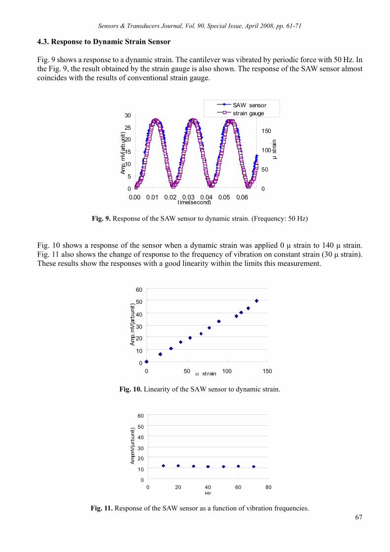
Sensors & Transducers Journal, Vol. 90, Special Issue, April 2008, pp. 61-71
67
4.3. Response to Dynamic Strain Sensor Fig. 9 shows a response to a dynamic strain. The cantilever was vibrated by periodic force with 50 Hz. In the Fig. 9, the result obtained by the strain gauge is also shown. The response of the SAW sensor almost coincides with the results of conventional strain gauge.
0
5
10
15
20
25
30
0.00 0.01 0.02 0.03 0.04 0.05 0.06t ime(second)
Amp.
mV(
arb.
unit)
0
50
100
150
μst
rain
SAW sensorstrain gauge
Fig. 9. Response of the SAW sensor to dynamic strain. (Frequency: 50 Hz) Fig. 10 shows a response of the sensor when a dynamic strain was applied 0 µ strain to 140 µ strain. Fig. 11 also shows the change of response to the frequency of vibration on constant strain (30 µ strain). These results show the responses with a good linearity within the limits this measurement.
0
10
20
30
40
50
60
0 50 100 150μ strain
Amp.
mV(
arb.u
nit)
Fig. 10. Linearity of the SAW sensor to dynamic strain.
0
10
20
30
40
50
60
0 20 40 60 80Hz
Ampm
V(ur
b.uni
t)
Fig. 11. Response of the SAW sensor as a function of vibration frequencies.
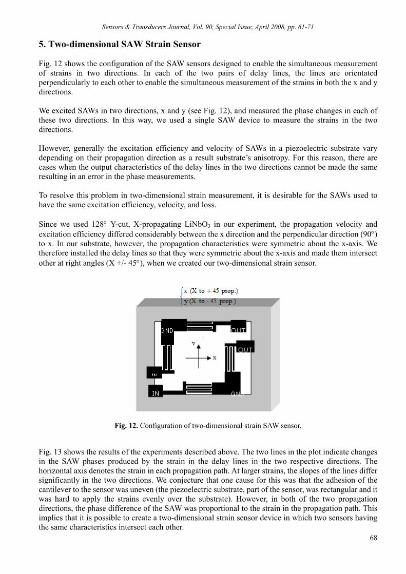
Sensors & Transducers Journal, Vol. 90, Special Issue, April 2008, pp. 61-71
68
5. Two-dimensional SAW Strain Sensor Fig. 12 shows the configuration of the SAW sensors designed to enable the simultaneous measurement of strains in two directions. In each of the two pairs of delay lines, the lines are orientated perpendicularly to each other to enable the simultaneous measurement of the strains in both the x and y directions. We excited SAWs in two directions, x and y (see Fig. 12), and measured the phase changes in each of these two directions. In this way, we used a single SAW device to measure the strains in the two directions. However, generally the excitation efficiency and velocity of SAWs in a piezoelectric substrate vary depending on their propagation direction as a result substrate’s anisotropy. For this reason, there are cases when the output characteristics of the delay lines in the two directions cannot be made the same resulting in an error in the phase measurements. To resolve this problem in two-dimensional strain measurement, it is desirable for the SAWs used to have the same excitation efficiency, velocity, and loss. Since we used 128° Y-cut, X-propagating LiNbO3 in our experiment, the propagation velocity and excitation efficiency differed considerably between the x direction and the perpendicular direction (90°) to x. In our substrate, however, the propagation characteristics were symmetric about the x-axis. We therefore installed the delay lines so that they were symmetric about the x-axis and made them intersect other at right angles (X +/- 45°), when we created our two-dimensional strain sensor.
Fig. 12. Configuration of two-dimensional strain SAW sensor.
Fig. 13 shows the results of the experiments described above. The two lines in the plot indicate changes in the SAW phases produced by the strain in the delay lines in the two respective directions. The horizontal axis denotes the strain in each propagation path. At larger strains, the slopes of the lines differ significantly in the two directions. We conjecture that one cause for this was that the adhesion of the cantilever to the sensor was uneven (the piezoelectric substrate, part of the sensor, was rectangular and it was hard to apply the strains evenly over the substrate). However, in both of the two propagation directions, the phase difference of the SAW was proportional to the strain in the propagation path. This implies that it is possible to create a two-dimensional strain sensor device in which two sensors having the same characteristics intersect each other.
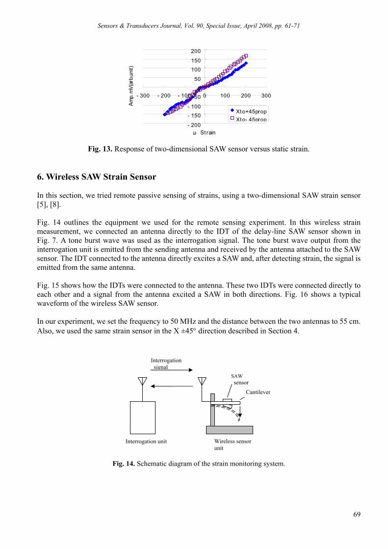
Sensors & Transducers Journal, Vol. 90, Special Issue, April 2008, pp. 61-71
69
- 200- 150- 100
- 500
50100150200
- 300 - 200 - 100 0 100 200 300
μ St rainAm
p. m
V(ar
b.uni
t)
Xto+45propXto- 45prop
Fig. 13. Response of two-dimensional SAW sensor versus static strain. 6. Wireless SAW Strain Sensor In this section, we tried remote passive sensing of strains, using a two-dimensional SAW strain sensor [5], [8]. Fig. 14 outlines the equipment we used for the remote sensing experiment. In this wireless strain measurement, we connected an antenna directly to the IDT of the delay-line SAW sensor shown in Fig. 7. A tone burst wave was used as the interrogation signal. The tone burst wave output from the interrogation unit is emitted from the sending antenna and received by the antenna attached to the SAW sensor. The IDT connected to the antenna directly excites a SAW and, after detecting strain, the signal is emitted from the same antenna. Fig. 15 shows how the IDTs were connected to the antenna. These two IDTs were connected directly to each other and a signal from the antenna excited a SAW in both directions. Fig. 16 shows a typical waveform of the wireless SAW sensor. In our experiment, we set the frequency to 50 MHz and the distance between the two antennas to 55 cm. Also, we used the same strain sensor in the X ±45° direction described in Section 4.
Fig. 14. Schematic diagram of the strain monitoring system.
Interrogation unit Wireless sensor unit
Cantilever
SAW sensor
Interrogation signal
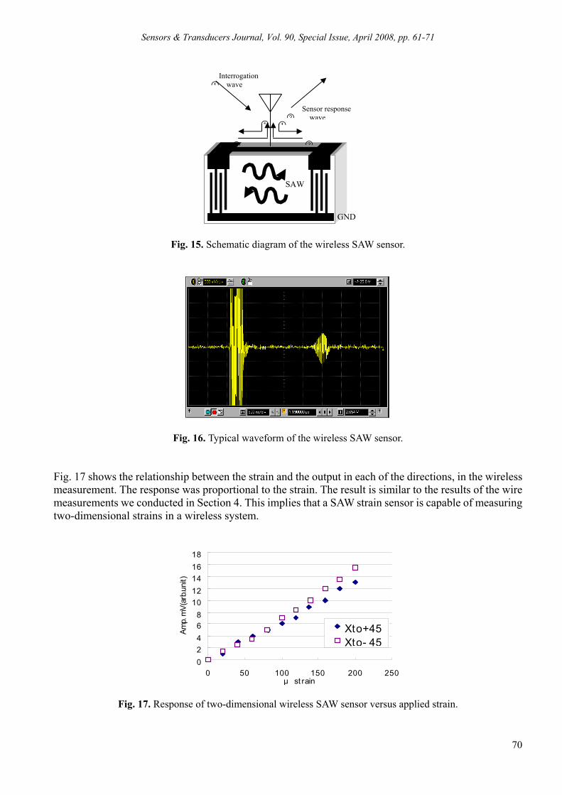
Sensors & Transducers Journal, Vol. 90, Special Issue, April 2008, pp. 61-71
70
Fig. 15. Schematic diagram of the wireless SAW sensor.
Fig. 16. Typical waveform of the wireless SAW sensor. Fig. 17 shows the relationship between the strain and the output in each of the directions, in the wireless measurement. The response was proportional to the strain. The result is similar to the results of the wire measurements we conducted in Section 4. This implies that a SAW strain sensor is capable of measuring two-dimensional strains in a wireless system.
02468
1012141618
0 50 100 150 200 250μ st rain
Amp.
mV(
arb.u
nit)
Xto+45Xto- 45
Fig. 17. Response of two-dimensional wireless SAW sensor versus applied strain.
Interrogation wave
Sensor response wave
①
① ①②
② ②
SAW
GND

Sensors & Transducers Journal, Vol. 90, Special Issue, April 2008, pp. 61-71
71
7. Conclusion This study proposed a strain sensor featuring a SAW device and investigated its characteristics. We obtained the following results: Changes in the phase of a SAW delay line are proportional to the strain in the propagation path. This enables strains to be measured using SAWs. We also demonstrated that, by placing two delay lines perpendicular to each other, we are able to measure strains in two different directions simultaneously. In such a case, by selecting the right propagation directions of the SAW, we can obtain similar characteristics in both directions. Finally, we connected the sensor to an antenna and conducted an experiment that showed that wireless, passive measurement of strains is possible. Acknowledgements This research was supported in part by Research Fund C of the Ministry of Education, Culture, Sports, Science and Technology of Japan. The authors wish to express their gratitude for this assistance. References [1]. V. K. Varadan, Microsensors, MEMS and NEMS for complex adaptive smart structures and systems, Smart
Materials and Structural Systems, No. 1-1, 2001, pp. 135-148. [2]. H. Wohltjen and R. Dessy, Surface acoustic wave probe for chemical analysis 1, Analytical Chem., Vol. 51,
No. 9, 1979, pp. 1485-1475. [3]. H. Wohltjen, Surface acoustic wave micro-sensors, Proc. of 4th International Conference on Solid-state
sensors and actuators, Tokyo, 1987, pp. 471-477. [4]. M. E. Motamedi and R. M. White, Special issue on acoustic sensors, IEEE Trans. UFFC., Vol. UFFC-34,
No. 2, 1987, pp. 122. [5]. A. Pohl, A review of wireless SAW sensors, IEEE Trans. UFFC., Vol. 47, No. 2, March 2000, pp. 317-332. [6]. D. Hauden, F. Bindler, R. Coquerel, SAW cantilever beam accelerometer sensitivities, Proceedings of IEEE
1985 Ultrasonics Symposium, 1985, pp. 486-489. [7]. H. Scherr, G. Scholl, F. Seifert and R. Weigel, Quartz pressure sensor based on SAW reflective delay line,
Proc. of 1996 IEEE Ultrasonics Symposium, 1996, pp. 347-350. [8]. J. Hayasaka, K. Tanaka, T. Miura, Y. Ikeda, and H. Kuwano, Wireless vibration sensor with a single-port
surface acoustic wave sensor, Proceedings of the 23rd Sensor Symposium, 2006, pp. 455-458.
___________________ 2008 Copyright ©, International Frequency Sensor Association (IFSA). All rights reserved. (http://www.sensorsportal.com)

Sensors & Transducers Journal, Vol. 90, Special Issue, April 2008, pp. 72-86
72
SSSeeennnsssooorrrsss &&& TTTrrraaannnsssddduuuccceeerrrsss
ISSN 1726-5479© 2008 by IFSA
http://www.sensorsportal.com
Environmental Measurement OS for a Tiny CRF-STACK Used in Wireless Network
Vasanth Iyer, G. Rammurthy, M. B. Srinivas
International Institute of Information Technology, Gachibowli, Hyderabad, (A.P.), India Tel.: -500 032 91-40-2300 1967, fax: 91-40-2300 1413
E-mail: [email protected], rammurthy, [email protected], http://www.iiit.net
Received: 15 October 2007 /Accepted: 20 February 2008 /Published: 15 April 2008 Abstract: To respond to the new development needs of sensor networks and their unique deployment, there are many available processors and varying target footprints for deploying sensor networks. The most common needs are supporting many different types of wireless radios and an environmental measuring operating system which allows interfacing to 8, 16 bit target microcontrollers. The constraints of the sensor nodes (that form the network) however, are that they have limited processing power, limited wireless range, limited memory, low data transmission rates and low cost packaging. The design of the software stack being proposed in this paper is based on the previous work by the authors who focused on implementation of Control Radio Flooding (CRF) protocol to self organizing sensor networks. The proposed stack, which is fully power-aware, is referred to as CRF-STACK. It integrates the hierarchical space partitioning tree with a data transaction model that allows seamless exchanges between data collecting sensors and its parent nodes in the hierarchy and could be compatible with emerging IEEE standards. This heart of model is a scalable real-time OS which allows a programming interface to develop sensor application and underlying radio communication. Through routing simulations we demonstrate that the energy-aware reusability of resources in sensor networks has a complexity where N is the total number of nodes. In sensor network the processing power for a given operation is typically measured as a collaborative processing of a group of nodes which is always higher than the individual sensors capabilities, the residual energy remaining of the sensor network at the end of the simulation is a good measure of the collaborative factor (lesser the residual value the better the collaborative factor). We show by simulation the optimal values for reusability to attain max lifetime converges without sensor faults for N <= 20% for CRF and LEACH-E. Even though LEACH-S results peak at routing N=5% it has a complex lifetime with errors with a residual energy after faults at 27.9%. To accommodate the lifetime with faults in the case of LEACH we extend this static sensor network model with a fault-recognition algorithm making the real-time values measured from sensors more fault resistant and reliable throughout its maximum life-time. Copyright © 2008 IFSA. Keywords: State machine stack, Sensor networks, Routing protocols, Fault recognition algorithms
Sensors & Transducers Journal, Vol. 90, Special Issue, April 2008, pp. 72-86
73
1. Introduction With the availability of low-cost sensor nodes there have been many standards developed to integrate and network these nodes to form a reliable network allowing many different types of hardware vendors to coexist. Most of these solutions however have aimed at industry-specific interoperability but not the size of the target footprint and the description of published standards usually run into hundreds of pages. In the proposed design we use a simple data transaction model which keeps the memory requirements low and configures the sensor network using CRF discovery protocol and routes the sensed data using an application specific polling rate. The heart of the design is a small foot print OS which implements a caching based energy-aware router which attains a peak collaborative factor, the implementation divides the rest of the sensors into 1-hop and 2-hop data sensing devices. These ad-hoc sensors are further made energy-aware which supports an agent (i.e. remotely accessible function) which uses low data rate wireless transmission, reduced duty cycle and uses data aggregation to enhances the battery life of the connected sensors. This design has to address the stack state machine to control the network messages and also integrate at the physical layer with different radios and the connected sensors which have real-time monitoring requirements. The underlying cooperative OS allows dedicated tasks for data collection and control of attached sensors. We use the seven layer OSI model for reference due to the tiny nature of the sensors the numbers of effective layers are reduced to mini four namely application, network, data-link and physical layers. Our protocol is dependent on the functionality of the target sensor as some of them need more data aggregation-specific requirements and others need to handle data routing needs. So the ROM and RAM requirements are the qualifying factors to tailor the functionality of the network layer or a scaled down bare minimum CRF-STACK [1] implementation for more passive sensors. As in any network environment, reliability and robustness are important part of the network design, we need to address self configuration of sensor networks as these are non-IP based and ad-hoc in nature. The existing body of research is currently focused on distributed infrastructure less multi-hop, clustering [5] and power-aware routing algorithms which have complete knowledge of the network but does assume any operating system complexity. In reality this assumption may not be true as the sensors need to be built from ground up with a power-aware maintainable operating system. In this work we enhance the previous work on LEACH by actually giving each sensor a reuse probability and measuring the mean residual before failure (loading per sensor) with varying percentages of cluster heads. Also we present a MAC level protocol CRF [2] which has adaptive low-complexity routing based on variable transmit power network discovery to partition the network into functional zones. The simulating the whole network (up to 100’s of nodes) to perform self-discovery, partition of the large network into functional zones, assign hierarchical network addressing and application targeted routing. The data transmission uses the B-tree with formed with all the sensor nodes and each edge of radius calculated by the CRF protocol. We show that the routing complexity cannot be balanced by increasing the resource availability but can actually degrade the expected performance, so there exists an ideal or fixed number of routers which need to be configured for any wireless sensor network to maximize its lifetime without failure for a given transmission throughput. The rest of paper is divided into three main sections, section one compares the light weight CRF-STACK with the standard OSI model, section two shows the functional implementation of CRF-STACK layers and the transaction model and section three shows the simulation routing performance results of the CRF protocol with and a fault recognition algorithm to detect false alarms due to faulty readings and concludes with hardware resources it needs to deploy on the target platform for a passive sensor or controllable implementation of the CRF-STACK.

Sensors & Transducers Journal, Vol. 90, Special Issue, April 2008, pp. 72-86
74
2. CRF and Environmental Partitioning and Deployment Control radius flooding (CRF) is a method for recursively (steps 1, 2, 3 in Fig. 1) subdividing an ad-hoc sensing region into zones sets by individual sensor flooding. The subdivision gives rise to a representation of the ad-hoc static sensors by means of a tree data structure known as CRF tree. It uses two criteria to make if energy efficient. The first it uses the minimal power needed from node-0 (coordinator-C) to flood its neighbors which is recursively repeated three times to form three forward zones joining the source to the distance sink. The second criteria is CRF uses a static cache (Zone 2) which for maximum energy efficiency needs to be 20% of the total number of nodes N. This split is shown in iteration 4 of the tree in green.
C
C
Z1 Z2
Zone 1
Zone 2
C
Z1 Z2
Zone 1
Zone
2
Zone 3
Z3
1 2 3
C
40% 20%
Zone 1
Zone
2
Zone 3
40%
4
C
Fig. 1. Partition of the sensing region into functional zones using recursive CRF protocol and the percentage of nodes after complete topology discovery.
3. Open Systems Interconnection (OSI) Model Open Systems Interconnection (OSI) model is a reference model developed by ISO as a framework of standards for communication in the network of different equipments. The OSI model defines the communication process into seven layers. The OSI model is capable of being used for wide area networks and, hence, it is more complex than what is needed for CRF-STACK. The stack features for the implementations of computer network and CRF-STACK protocols are compared in Table 1. Inspired by these unique requirements, we propose our protocol stack with four layers namely application, network, data link, and physical layer. In the proposed model, we compress the existing CRF protocol into the network layer and the data link layers. The upper three layers of the OSI model

Sensors & Transducers Journal, Vol. 90, Special Issue, April 2008, pp. 72-86
75
could be merged into one layer that is called application sensing layer which handles zone creation and data aggregation. The physical layer and the MAC layers implements the CSMA-CA protocol and a hardware abstraction layer (HAL) is implemented to use any type of radios and also to interface to any real-time sensors.
Table 1. OSI (Vs) CRF-STACK
4. Design of Protocol Stack Each layer of the proposed protocol stack is divided into both transmit and receive only parts. Stack size of at least 55Kbytes is required for a full CRF-STACK and < 20Kbytes for a passive sensor. 4.1. Application and Sensing Layer This layer is the highest layer of the protocol stack. In a CRF-STACK environment, each sensing node is pre-configured (hard coded) to comply with its ROM and RAM sizes and the zones they are located to be a fully functional aggregator, a router or a tiny passive sensor. This layer implements the CRF zoning to split the whole network into three functional zones. Zone-one has tiny passive sensors and uses a single hop to connect to the parent data aggregator (which is normally considered as node-0), zone-two has routers with full CRF-STACK capable of acting as a cluster head [5] and zone three has tiny passive sensing devices. The monitoring only stack has real-time extensions to the OS scheduler to manage dedicated sensing activity to periodically collect the sensed data to be communicated over the stack. 4.2. Network Layer The most important responsibility of this layer is routing of sensed data to a central aggregator. To accomplish the design goals of supporting a hierarchical tree routing with zone hopping (multi-hopping), a bare minimum protocol needs to be defined. The network layer also can handle large amounts of nodes with low latencies and without the use of high power transmitters. To add a new protocol on top of CRF one has to know the data flow and extend the appropriate addressing to support large number of nodes in a zone partitioned network. For simplicity to satisfy the data rate of the application we assume a traffic model which, at an application defined rate, updates the newly read

Sensors & Transducers Journal, Vol. 90, Special Issue, April 2008, pp. 72-86
76
sensor values and routes to a central aggregator. We first choose the addressing scheme. In this hierarchical topology we use two types of addressing: one is a unique 64 bit long address and the other a 16 bit short address. The addressing mode is source/destination identifier for peer to peer communication; typically the parent and the central aggregator have long addresses and the children are assigned short addresses. The long addresses are unique over multiple networks as each network can have up to 216 (65,535) sensor nodes. Thus a single network is always addressed in three zone format, parents (long address), siblings (long address) and children (short address). To address application-specific data flow with a basic transaction (data aggregation schedule) to accomplish these on a wireless medium, where only one node can transmit data at a given time, we need to see the data flow using a beacon and a beacon-less system. A beacon is generally used to detect new sensors on the network and register them as part of the network or to allow existing sensors to update their new data. The shorter the beacon time the shorter is the node detection time of the overall network. But as the beacon period is reduced, more capacity is used for beacon transmission. As all the data collecting sensors are located in zone three and zone one we need a beacon based system for scheduling the sensors to wake up and collect the new data and send it to its parent. Also, this beacon system can discover new sensors and assign them a short address. In a sensing application there are two types of needs: in the first case the data needs to be gathered only when needed and the rest of the times sensors are put to sleep saving valuable battery power. In the second case the application has some measured threshold such as if is there is a change in measured-delta then only the data is forwarded to the central aggregator thus saving redundant packets. Both these transaction needs can be addressed: the first uses a beacon based time slot the other uses non beacon based data trigger to forward the packets. Having decided on the basic structure of transactions to enhance CRF, one needs to define a packet format for transaction between sensor and cluster heads as shown in Fig. 3. This message format is defined in Fig. 2 to suit a low data rate, low latency requirement. To keep it light weight, we define a simple implementation. GENFRAME definition has the protocol CRF data packet as well as MAC standard envelope which we call as CRFPKT. 1. Protocol version(one byte) 2. Flags (one bit each) 3. Command 4. Response 5. Error 6. Sequence and acknowledgement 7. Data length (two bytes) 3.2.1. Packet Format
Fig. 2. Simple protocol packet for CRF.
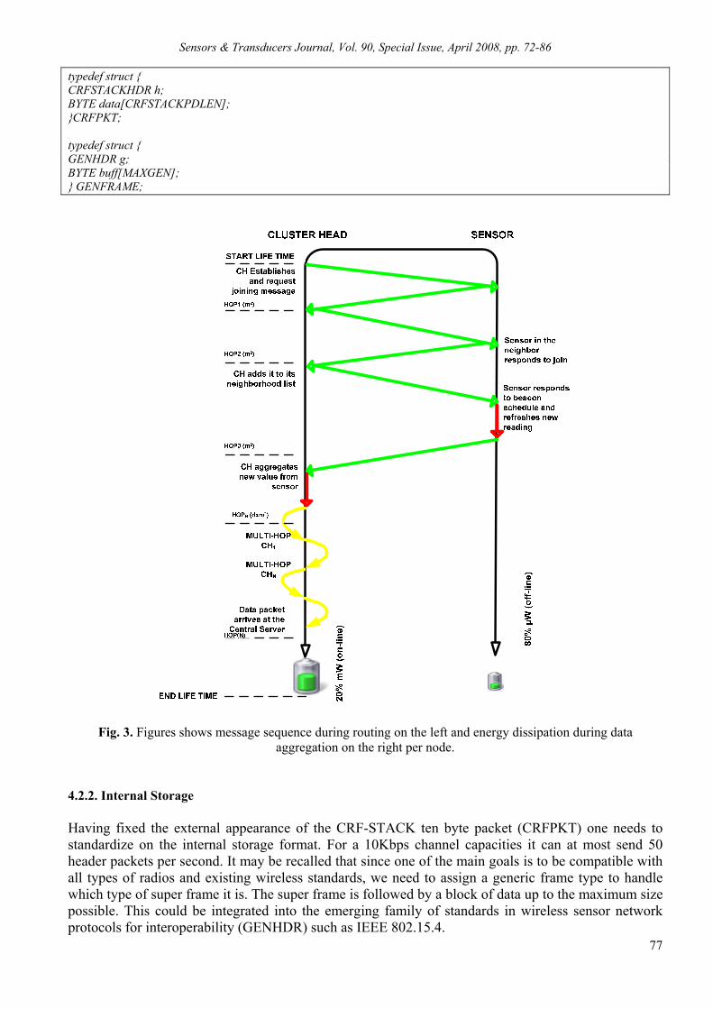
Sensors & Transducers Journal, Vol. 90, Special Issue, April 2008, pp. 72-86
77
typedef struct CRFSTACKHDR h; BYTE data[CRFSTACKPDLEN]; CRFPKT; typedef struct GENHDR g; BYTE buff[MAXGEN]; GENFRAME;
Fig. 3. Figures shows message sequence during routing on the left and energy dissipation during data aggregation on the right per node.
4.2.2. Internal Storage Having fixed the external appearance of the CRF-STACK ten byte packet (CRFPKT) one needs to standardize on the internal storage format. For a 10Kbps channel capacities it can at most send 50 header packets per second. It may be recalled that since one of the main goals is to be compatible with all types of radios and existing wireless standards, we need to assign a generic frame type to handle which type of super frame it is. The super frame is followed by a block of data up to the maximum size possible. This could be integrated into the emerging family of standards in wireless sensor network protocols for interoperability (GENHDR) such as IEEE 802.15.4.

Sensors & Transducers Journal, Vol. 90, Special Issue, April 2008, pp. 72-86
78
4.2.3. Addressing Since this layer assigns hierarchical addressing, we need to incorporate it into the existing packet format as defined in Fig. 4 to route uni-cast, broad-cast and multi-cast operations. We have already defined two types of addressing, long and short addressing. To get the long address of the parent the child nodes can query the sibling and its next multi-hop parent to resolve the complete destination path.
Dest Srce Pcol Ver Flag Seq Ack Dlen Data
Fig. 4. Addressing CRF routing. From Table 2, the usage of short and long addressing used by CRF-STACK protocol can easily be understood.
Table 2. Addressing mode between motes.
From To
123456789ABC FFFFFFFFFFFF
3456789ABCDE 123456789ABC
123456789ABC 255
Broadcast
Parent tosibling
Parent tochild(shortaddress)
4.4. Data Link Layer This layer is cluster aware and holds the neighborhood table as this has the entries of all the children (zone III). The layer has full knowledge and control of one hop neighbors. As shown in Fig. 1, a beacon based refresh mechanism is used to keep track of all the connected sensors. The main functionally of the layer is discovering new sensors, scheduling data aggregation for all the child nodes and power management by using the sensor nodes to be on (duty cycle) when acquiring new data defined by an application beacon rate. The MAC implements the localization, mobility and neighbor list. On top of these it does power control i.e. the amount of transmitted power range it needs to assign for a given sensor node as shown Fig. 5 which is calculated by CRF on-line clustering algorithm. Currently since there is no standard, it can be anywhere between 10-100 meters which is practical for indoor deployment but for high density sensor networks it needs to be specially adjusted which is called special density of the covered region. A good topology discovery algorithm is to find the density of the network and use flooding and create a neighbor list. CRF implements control flooding i.e. if a node is already in the neighbor list it can flood within its RF range but a newly discovered node cannot until it is added to the list for the next iteration of flooding. This process is repeated three times as our need is to split the topology into three separate zones with always connected end zones with a caching middle zone. At the end of the discovery phase the complete range is found out which is a single hop from the farthest node to the central aggregator and the neighbor list contains all the address of the single hop parent and all the

Sensors & Transducers Journal, Vol. 90, Special Issue, April 2008, pp. 72-86
79
siblings have the addresses of the child nodes. This flooding is performed only during the initial discovery phase typically started by FormNetwork-API (Fig. 10).
Fig. 5. MAC and its differential radio power control dependencies. 4.4. Physical layer Physical layer consists of spread spectrum radio technology which transmits a signal to a much wider range of frequency band. To a narrow band receiver, the transmitted signal is impossible to detect as it appears as low-level noise. However, a wide band receiver can monitor the whole frequency band and detect changes. The overall goal of this layer is to use an emerging standard to make the radios interoperable. 4.5. Hardware Abstraction Layer (HAL) This is a BIOS (Basic input-output) dependent layer which controls the input, output LEDs and sensors connected to each mote. As the stack size is of a critical concern no additional tasks are running inside the motes so the network stack allows call back functions to control the connected sensors and acquires the readings without OS buffering. The target specific API’s are compiled for each build which implements specific hardware interfaces. 4.6. Simulation and Cross Layer Optimizations The protocol stack used by the central aggregator is dependent on all the underlying layers of the stack that contains software and hardware only implementations. Since the hardware layers are non-programmable, it is best to use the specification for low cost, low memory and low data rate requirements. In the case of software, layers starting from the application sensing are very closely dependent on the type of application specific traffic and the available bandwidth which leads to the term cross layer optimization in sensor network applications. As the topology of CRF is static, once discovered it seldom changes making it easier to tune the parameters for addressing large sensor networks, multi-hop tree routing and data aggregation model for localized sensing. By simulation which implements the stack layers and a battery model (except the channel access protocol), we show that these parameters achieve optimal savings over the complete life-time of the sensor network when routing data packets. The simulation results are compared on two optimal criteria. The first is the

Sensors & Transducers Journal, Vol. 90, Special Issue, April 2008, pp. 72-86
80
maximum number of rounds which can be achieved by a routing algorithm which is shown in Table 3 and then the same results are extended to find residual energy dissipation which calculates how evenly does the distributed algorithm fair in terms of energy drain per node (reliability) as shown in Fig. 6 as opposed to peak performance (max rounds) in our previous case.
Fig. 6. MAC and its differential radio power control dependencies.
Table 3. Routing results for varied percentage of cluster and their residual energies.
Algorithm Percentage of clusters
(reusability)
Round the first node dies
(max lifetime)
Residual Energy Dissipation
(Collaborative factor) (Convergence↓)
LEACH-S 5% 10,736 27.90%
( Random Probability, 0.2 CH & 0.8 nodes) 10% 8992 38%
20%* 9681 36%
30% 8535 46%
40% 8894 50%
50%¥ 10,836 49%
LEACH-E 5% 17,602 0.97%
(Ø - Threshold ) 10%*¥ 15,604 0%
20% 15,351 1.74%
30% 15,395 15%
40% 13,824 32.50%
50% 7932 64.10%
CRF Zone1Zone2Zone3
( Fixed caching 1/3 rd) 5% 30% 5% 14,580 22.17%
10% 30% 10% 14,234 8.79%
20% 30% 20%* 15,227 6.04%
30% 30% 30% 14,585 10.22%
40% 30% 40%¥ 17,214 7.45%
50% 30% 40% 14,615 20.01%

Sensors & Transducers Journal, Vol. 90, Special Issue, April 2008, pp. 72-86
81
3.7. Routing Comparison of Energy Efficiency Versus Cluster sizes The wireless sensor simulator [6] allows picking the number of cluster heads in each simulation run and the type of distributed algorithm used such as LEACH, LEACH-E and CRF. In this experiment for each lifetime run (up till the 1st sensor dies) for a routing algorithm the percentage of cluster heads is gradually increased from 5% up to 50%. The results are plotted as seen in Fig. 7. LEACH-S which is the standard [5] implementation of the paper in 2001 from MIT which is shown in Table 3 as expected it linearly increases as the number of cluster heads increases. But in the case of the energy adapted version LEACH-E and CRF it is optimal when the percentage of cluster heads are at 5% and 40%. Here we cross-verify the results and show that for energy efficiency in minimum loading per node in the case of LEACH-E and CRF and converges without error at N <=20 as shown in Fig. 7.
Fig. 7. Lab results shows residual energy dissipation impact loading on the whole network for distributed routing algorithms compared to direct transmission(always 100% loading).
The adaptive versions of LEACH are LEACH-E for energy centric threshold and CRF which uses a static cache. In both the cases loading is minimal (Fig. 6 shows the data points in percentage of remaining residual power) and highly fault tolerant when the percentage of cluster heads are set to 20% as shown in figure (0% for LEACH-E and 6.04% for CRF). This result highlights the fact that the energy dissipation is network size invariant and always divides the sensor nodes into 80-20 rule which is 80% of the nodes are idle and 20% does the real routing. 4.6. Routing Comparison of Energy Efficiency Using Multi-hop Algorithms These families of routing algorithms are non-cluster based. To verify with other routing algorithms which are non cluster based as simulated before we use a multi-hop based routing which implements the following forward one hop routing algorithms. These algorithms are based on each hop logic and they decide on how to branch or navigate the densely connect mesh of the sensor network. The can be further divided according to path logic used, minimum spanning tree which visits a node only once and has no cycles, Power-aware hop which uses the most non-used path with high remaining residual energy and the short-path which takes the quickest path available between source to sink. Fig. 8 shows that when compared to CRF (cached based routing) the multi-hop version does far below the expected values in terms for maximum number of rounds completed. The MST comes closest to CRF followed by worst cases results in MH-PA and MH-SH.

Sensors & Transducers Journal, Vol. 90, Special Issue, April 2008, pp. 72-86
82
Fig. 8. Lab results shows number of rounds for clustering, multi-hop and on-demand algorithms. 5. Fault Recognition Model for Sensor Data Aggregation The model uses Bayes posterior estimation by introducing two types of expected errors.
(1)
It is true, however, that the sensor measurements in the operation region are spatially correlated (since many environmental phenomena are). The first namely the electronic sensor faults which are uncorrelated [3] with the sensor measurement and the other which is based on the total unattended life-time of the sensor network or simply load balancing errors. One can define the total unattended life-time of the sensor network as
Using equation (1) we can estimate the probability before the 1st sensor dies given by equation when it is tamely faulty.
(2)
(3)
We will say that we are trying to find the correction c, out of all possible corrections, that maximizes the probability of c given the original measurement M:
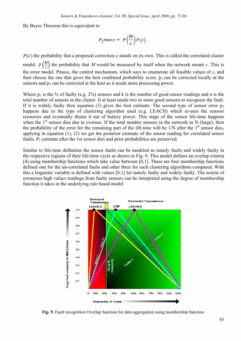
Sensors & Transducers Journal, Vol. 90, Special Issue, April 2008, pp. 72-86
83
By Bayes Theorem this is equivalent to
the probability that a proposed correction c stands on its own. This is called the correlated cluster
model. the probability that M would be measured by itself when the network meant c. This is the error model. Pmaxc, the control mechanism, which says to enumerate all feasible values of c, and then choose the one that gives the best combined probability score. p1 can be corrected locally at the sensors and p2 can be corrected at the host as it needs more processing power. Where p1 is the % of faulty (e.g. 2%) sensors and k is the number of good sensor readings and n is the total number of sensors in the cluster. It at least needs two or more good sensors to recognize the fault. If it is widely faulty then equation (3) gives the best estimate. The second type of sensor error p2 happens due to the type of clustering algorithm used (e.g. LEACH) which re-uses the sensors resources and eventually drains it out of battery power. This stage of the sensor life-time happens when the 1st sensor dies due to overuse. If the total number sensors in the network in N (large), then the probability of the error for the remaining part of the lift-time will be 1/N after the 1st sensor dies, applying in equation (1), (2) we get the posterior estimate of the sensor reading for correlated sensor faults. P2 estimate after the 1st sensor dies and prior probabilities are preserved. Similar to life-time definition the sensor faults can be modeled as tamely faults and widely faulty in the respective regions of their life-time cycle as shown in Fig. 9. This model defines an overlap criteria [4] using membership functions which take value between [0,1]. These are four membership functions defined one for the un-correlated faults and other three for each clustering algorithms compared. With this a linguistic variable is defined with values [0,1] for tamely faulty and widely faulty. The notion of erroneous high values readings from faulty sensors can be interpreted using the degree of membership function it takes in the underlying rule based model.
Fig. 9. Fault recognition Overlap function for data aggregation using membership function.

Sensors & Transducers Journal, Vol. 90, Special Issue, April 2008, pp. 72-86
84
6. Environmental Measurement Real-Time OS To implement the CRF-STACK for a given target embedded processor we need to comply with the available ROM and flash memory resource availability. The current stack size including HAL layer takes up to < 50kbytes. The comparison for specific compiler and functional requirements and its target sizes are seen in Fig. 10. The functional differences and resource requirements needed to store neighbor tables and implement dedicated sensor tasks are discussed in section 7. Tools needed to configure and program an embedded system are a target based compiler which means that one needs an M×N number of compilers where M is the number of target processors and N is the number of supported languages. As this is a huge number we standardize on ANSI-C for portability purposes as most of embedded compilers support this low-level language. This makes use of M compliers to support all available sensor targets. The parameters which are target dependent are listed below in Table 4. Most of the sensors have specific ROM, RAM and additionally a flash interface built in. The current architecture allows to add a multi-tasking OS [5] which could be ROM resident with most of it kernel services and runtime libraries. As CRF-STACK are state machines and could be adapted to be re-entrant (if the application must run the FSM from multiple independent threads and the FSM code must only process a single transition and then return).
Table 4. Energy-aware stack simulator.

Sensors & Transducers Journal, Vol. 90, Special Issue, April 2008, pp. 72-86
85
20Kb
50Kb
Mem
ory
requ
irem
ents
ControllersRouter
PassiveSensors
Comparison of targetspecification for HI-
TECH PICC processor
unsigned short task_stack[200];const ROM_TCB task_rom_list[]=main,0,0,Sensetsk1,&task_stack[50],2,Sensetsk2,&task_stack[100],3,;
int main (void)byte status;
K_OS_Init(); //init OSstatus = K_Task_Create(TASK1_ID);status |= K_Task_Create(TASK2_ID);while (status);
for(;;);;
Multi-tasking forsensing needs
Fig. 10. Stack size for different sensor footprint needs and the program for tiny multi-tasking.
With these modifications some of the static data can be loaded into ROM and the remaining could be fit into available RAM. The multi-tasking feature can service sensor events or periodically aggregate data which could be queried by the top level application and send over the stack. The complexity of the program and its resource
requirements is dependent on the routing, aggregation algorithms or data logging periodicity needs. 7. Benefits of Energy-awareness in the OS Measurement Shown below are the energy management parameters available to the simulator at each level. 1. TOPOLOGY LEVEL: Ø-threshold based cluster head selection (Caching)…… 2. TOPOLOGY LEVEL: Optimal number of clusters (Power Law)……………… 3. TOPOLOGY LEVEL: Density of sensor network (K-neighborhood distance)… 4. TOPOLOGY LEVEL: Routing overhead – …………………………. 5. DATA LINK: BEACON duty cycle, synchronization--------------------------- 6. DATA LINK: Data aggregation & compression (Lossy Model)-------------------- 7. DATA LINK: Adjustable Transmit range (Redundancy=less power) -------------- 8. PHYSICAL LAYER: Low bandwidth, Data rate/ bit--------------------------------- 9. OS-KERNEL: Sensing scheduler (less contention=less power)--------------------- 10. OS-KERNEL: IDLE time scheduler(less usage=less power)----------------------- 11. OS-KERNEL: Low footprint(low memory reqd.=less power) --------------- 8. Conclusion In this paper we have addressed how to implement a tiny protocol and a portable stack for R&D and simulation of large sensor networks which uses cluster based routing protocols and multi-hop protocols. The network layer and the data link layer use all the cross layer optimization to achieve specification requirements and extends the real-time kernel services to implement time critical and sensor specific tasks to achieve a better design. Each of these routing categories clustering and multi-hoping finds specific application advantages based on the type of deployment one is periodic and other mostly reactive networks. Also it models a cluster fault recognition algorithm to better predict and rectify false alarms when a routing algorithm does not converge in a simple lifetime and erroneous sensor measurements. We also prove from the results that the resource problem in sensor network is scale invariant and converges when N<=20%. By uniquely dividing the load and by adjusting the cluster size we could extent this reliability model to all the previous work on sensor network into fuzzy model to predict the max lifetime to distributed complexity of each power-aware algorithm.
Classification
Sensing

Sensors & Transducers Journal, Vol. 90, Special Issue, April 2008, pp. 72-86
86
Acknowledgements Authors are grateful to Dept. of Science and Technology-DST, Govt. of India, for supporting the work with a grant. Also like to thank M.S. student Agarwal .M for helping us on the interoperability of network on chip and Dr. Bertrand from CCT, Switzerland for identifying a suitable application for real deployment. References [1]. Software Stack Architecture for Self-Organizing Sensor Networks, Vasanth Iyer, Rama Murthy and M. B.
Srinivas- ICST 2007, Palmerston North New Zealand. [2]. Vasanth Iyer, Rama Murthy, M. B. Srinivas, Information Processing of Wireless Sensor Networked Motes
by Harvesting Residual Power, The Second IEEE International Workshop on Next Generation Wireless Networks 2006 (IEEE WoNGeN 2006).
[3]. Efficient and Fault-Tolerant Feature Extraction in Wireless Sensor Networks Bhaskar Krishnamachari and S. Sitharama Iyengar.
[4]. Dr. Ramamurthy, Distributed Wireless Sensor Network Architecture: Fuzzy Logic based Sensor Fusion, Vasanth Iyer, EUSFLAT, Sep 11-14th 2007, Ostrava, Czech Republic.
[5]. Wendi Heinzelman, Hari Balakrishnan, LEACH (Low Energy Adaptive Clustering Hierarchy), Anantha Chandrakasan, 2001.
[6]. Simulator for download at http://www.geocities.com/ids_lab/crf.zip
___________________ 2008 Copyright ©, International Frequency Sensor Association (IFSA). All rights reserved. (http://www.sensorsportal.com)

Sensors & Transducers Journal, Vol. 90, Special Issue, April 2008, pp. 87-99
87
SSSeeennnsssooorrrsss &&& TTTrrraaannnsssddduuuccceeerrrsss
ISSN 1726-5479© 2008 by IFSA
http://www.sensorsportal.com
Ubiquitous Healthcare Data Analysis and Monitoring Using Multiple Wireless Sensors for Elderly Person
1Sachin Bhardwaj, 2Dae-Seok Lee, 3S. C. Mukhopadhyay and 4Wan-Young Chung
1Dept. of CSE&IT, Institute of Technology and Management, Sector 23-A, Gurgaon-122017, Haryana, India
2Dept. of Ubiquitous IT, Graduate School of Design & IT, Dongseo University, Busan 617-716, Korea 3Institute of Information Science & Technology, Massey University, Palmerston North, New Zealand
4Division of Computer and Information Engineering, Dongseo University, Busan 617-716, Korea E-mail: sanusachin, [email protected], [email protected],
Received: 15 October 2007 /Accepted: 20 February 2008 /Published: 15 April 2008 Abstract: Increasing life expectancy accompanied with decreasing dependency ratio in developed countries calls for new solutions to support independent living of the elderly. Ubiquitous computing technologies can be used to provide better solutions for healthcare of elderly person at home or hospital. Also, data fusion from multiple sensors shows itself the capability to have better monitoring of person. In this paper work, the healthcare parameters as like ECG and accelerometer are used to give a better treatment to the elderly person at home or hospital. Accumulated vital signs data through long-term monitoring is a valuable resource to assess personal health status and predict potential risk factors through the fusion monitoring of multiple sensors. The hardware allows data to be transmitted wirelessly from on-body sensors to a base station attached to server PC using IEEE802.15.4. If any abnormality occurs at server then the alarm condition sends to the doctor’s personal digital assistant (PDA). The system provides an application for recording activities, events and potentially important medical symptoms. Copyright © 2008 IFSA. Keywords: ECG, Accelerometer, QRS-Complex, P-wave, T-wave, Acceleration norm, Orientation angle, Ubiquitous healthcare 1. Introduction Reliable health monitoring requires the integration of research in the diverse fields of instrumentation, data acquisition storage, signal processing, approximate reasoning, feature extraction techniques and

Sensors & Transducers Journal, Vol. 90, Special Issue, April 2008, pp. 87-99
88
multi-sensor data fusion. Data fusion is the synergistic use of information from multiple resources in order to assist in the overall understanding of the condition of a system. It offers a more complete figure of the whole situation and more accurate evaluation of the condition based on the information from individual sensors. Recent advances in sensor technology allow continuous, real-time ambulatory monitoring of multiple patient physiological signals including: ECG, body temperature, respiration, blood pressure, oxygen levels, and glucose levels [1], [2]. These systems are conveniently packaged as a single product and could be used to give a complete picture of the patient health. However they generate large amounts of patient data that must be intelligently analyzed and archived to be most useful. In previous studies, home telecare systems using non-continuous monitoring and telephone data transmission [3], [4] have already proven effective in the management of chronic diseases such as congestive heart failure and hypertension. Continuous monitoring would allow telecare systems to accommodate a larger number of pathologies including asymptomatic conditions like atrial fibrillation for which intermittent monitoring is not sufficient. Technology that would allow healthcare providers to deploy, configure, and manage such monitoring systems, would provide a tremendous service to the healthcare industry while at the same time improving the quality of life for thousands of patients. Numerous heart diseases can be detected by means of analyzing electrocardiograms (ECG) and the changes in heart rate occur before, during, or following behaviour such as posture changes, walking and running. Therefore, it is often very important to record heart rate along with posture and behaviour, for continuously monitoring a patient’s cardiovascular regulatory system during their daily life activity. Falling is also one of the most significant causes of injury for elderly citizens or patients. By utilizing acceleration values corresponding to the user’s body motion, the system can also detect the fall of elderly person or patient. Our system developed an robust platform for real-time fusion monitoring of multiple sensors for patients staying in their home or hospital and transmitting health data to doctors working at the hospital with extended ECG [5] and acceleration analysis [6], [7]. The changes in heart rate occur before, during, or following behaviour such as posture changes, walking and running. Therefore, it is often very important to record heart rate along with posture and behaviour, for continuously monitoring a patient’s cardiovascular regulatory system during their daily life activity. The ECG and accelerometer data are continuously recorded with a built-in automatic alarm detection system, for giving early alarm signals even if the patient is unconscious or unaware of cardiac arrhythmias [8]. Emphasis is placed on recent advances in wireless ECG system for cardiac event monitoring and behaviour monitoring such as walking, running with fall detection of patient [9]. An accelerometer data for supporting the ECG analysis gives some detail about the effects of motion while the person is in the motion or fall down. Fig. 1 shows the system architecture of fusion monitoring of ECG and accelerometer sensors for ubiquitous healthcare system. The system also provides an application for recording activities, events and potentially important medical symptoms. The hardware allows data to be transmitted wirelessly from on-body sensor to the base system and then to PC/PDA. After receiving the serial data received from the base station node attached to server, ECG and accelerometer data are analyzed, which includes searching the QRS-complex, P-wave, T-wave and calculating the norm and orientation angle, in real time. Server/Client software programs were developed in C# based on .Net compiler for monitoring and analyzing the ECG and Accelerometer recordings. For ECG analysis, QRS detection algorithm is based on the originally developed QRS detection algorithm by Pan-Tompkins [10] in assembly language for implementation on a Z80 microprocessor and later improved and ported to C by Hamilton and Tompkins [11]. This QRS detector uses a signal ECG channel and was originally designed to operate at 200 Hz. The advantages of this QRS detection

Sensors & Transducers Journal, Vol. 90, Special Issue, April 2008, pp. 87-99
89
algorithm are that it is efficient and easily modified for different sample rates. This algorithm is improved according to our software analysis requirement and is developed in C#.net language to comfort with P and T-wave detection and accelerometer analysis at server. If any abnormality occurs at server then the alarm condition sends to the doctor’s PDA.
Fig. 1. System architecture for fusion monitoring of ECG and accelerometer sensors. 2. System Designing Sensing technology plays an important role to assist an elderly person or patient. The concept of ubiquitous healthcare system placed unobtrusive sensors on patient’s body to form a fusion data monitoring. An ECG and accelerometer sensors are attached to the human body and transmitting data to the base station. Heart rate, norm, orientation and other parameter of ECG are calculated with fall detection on server. After detection an abnormal ECG or fall of elderly person or patient then alarm condition sends to the doctor’s PDA. Flow chart of ECG and accelerometer signal analysis is shown in Fig. 2.
Fig. 2. Flow chart for ECG and accelerometer data monitoring and analysis.

Sensors & Transducers Journal, Vol. 90, Special Issue, April 2008, pp. 87-99
90
2.1 QRS Detection QRS detection is based on the analysis of slope, amplitude, and width of QRS complexes. It includes a series of filters and methods that perform low pass, high pass, derivative, squaring and integration procedures. Filtering reduces false detection caused by the various types of interference present in the ECG signal. This filtering permits the use of low thresholds, thereby increase the detection sensitivity. The algorithm adjusts the thresholds automatically and parameters periodically to adapt the changes in QRS morphology and heart rate. The flow chart for QRS-complex, P-wave and T-wave detection algorithm is shown in Fig. 3.
Fig. 3. P, QRS and T wave detection algorithm. By using moving window integration process, we can calculate R-R intervals, width of QRS complex and heart rate variability. Heart rate is computed by measuring the length of the R-R interval, or a full period of the waveform. These parameters are used to detect abnormality in patients. 2.2 P-wave and T-wave Detection P-wave and T-wave detection algorithm searches for the T-wave first, after a QRS-complex has been detected. The wave is expected within a specific time window. The start and end duration of window depends on the R-R interval: If the R-R interval>0.7 second: T-wave Window begin = 0.08 sec after QRS end. T-wave window end = 0.004 second. If R-R interval<0.7 second: T wave window begin = 0.04 second. T wave window end = (0.7R-R interval -0.06) sec.

Sensors & Transducers Journal, Vol. 90, Special Issue, April 2008, pp. 87-99
91
Within this window, the minimum, maximum and order of the slope of the derived function are important for detecting the T-wave. Bi-phase T-wave can be identified in the same way. The change of slope, as well as the end of the T-wave, is detected based on thresholds. The slope must include positive and negative values and the slope magnitude needs to be at least 0.006 mV/s for a T-wave to be detected. The algorithm searches for this combination, until the beginning of a new QRS complex is detected. If SlopeTwave[t-1]> SlopeTwave[t] then the slope is negative and if SlopeTwave[t-1]<SlopeTwave[t] then the slope is positive. It will check for five consecutive slopes then can decide finally positive and negative slope. Where p is the number of slope encounter and SlopeTwave is the calculated slope during T-wave detection. Initially, the value set as t=1 and SlopeTwave[0]=0. The detection rule for a P-wave is a positive slope followed by a negative slope. The magnitudes of both slopes have to be greater than 0.004 mV/s. The algorithm searches for this combination, until the beginning of a new QRS complex is detected. After detecting a QRS complex then it is deleted and replaced with the base-line. The base line is determined by analyzing a few samples preceding the QRS complex. The resulting signal is band pass filtered with -3 dB points at 3 Hz and 11 Hz and the search interval is defined as QTmax =2RR/9+250 ms, where RR is the interval between two successive QRS complexes. The signal is rectified and threshold at 50 % and 75 % of the maximum to obtain a three level signal. After taking a cross correlation of the result computed with three levels signal and from a representative set of P waves. The peak in the cross-correlation corresponds to the location in the original ECG. Estimated P-R interval should be less than 0.02 sec for normal ECG, which extends from the beginning of the P wave to the first deflection of the QRS complex. 2.3 Accelerometer Norm and Orientation Calculus If Xi, Yi and Zi are the acceleration values at a particular instant of time then acceleration norm An is given as An = √(Xi
2+Yi2+Zi
2) and the orientation is calculated using the dot product of the norm and the vertical axes CosΘ = Zi/An The data collected at the base station attached to PC are the sample level values in the range [0, 4096] of the voltage signal from sensor unit. So for calculating the acceleration from these samples first voltage level is calculated and checks weather this voltage level is for positive acceleration or negative acceleration. The formula used for calculating using the exact acceleration values is given as V.L. = [(VDD(mV)*Sample Level)/4096- 500(mV)] ,
200(mV) where 1500 mV is the reference voltage level of the accelerometer, above this level is positive acceleration and below is negative acceleration and 200 mV/g is the sensitivity of the accelerometer. After calculating all parameter of ECG signal then can classify shape and beat of ECG. For example, in rest if the heart rate is greater then 100 then is called sinus tachycardia disease and if the heart rate is lees then 60 then it is called a sinus bradycardia disease. If the heart rate is in between 60 and 100 then it is a normal sinus rhythm. But it is not sure during moving activity of patient, which is shown in Fig. 4. The moving activities (walking and running) of patient is recorded in experiments up to acceleration norm value 3g (where g = 9.8 m/s2).

Sensors & Transducers Journal, Vol. 90, Special Issue, April 2008, pp. 87-99
92
Fig. 4. ECG analysis with activity monitoring Basically, the algorithm developed using acceleration sensor decides fall detection. When people fall, acceleration is rapidly changed, according to their changes algorithm can classify the status of patient. Fall can be detected by measuring large acceleration threshold and orientation horizontal with ground within a time interval. The functionality behind this method was to observe a significant changes in the user’s orientation angles, look for a large acceleration within the same time interval, and when both are present, classify as a fall which is shown in Fig. 5. If the resultant value is greater than acceleration threshold value for continuously 15 seconds then analyze the orientation angle. If the orientation angle is horizontal with ground (90 degree) then classify as a fall. Wait for 15 seconds more if the orientation angle is not horizontal with ground but deviated towards ground. If there is no activity encounter in the orientation angle and resultant value then consider as a fall.
Fig. 5. Fall detection and activity monitoring algorithm.

Sensors & Transducers Journal, Vol. 90, Special Issue, April 2008, pp. 87-99
93
3. Experimental Results Our experimental set-up obtains the ECG and accelerometer data from the sensors placed on real human body and MIT-BIH arrhythmia database [12]. Firstly data are transmitted from human body to base station and then to server for ECG and accelerometer analysis. According to server analysis, if there is any abnormality then sends alarm condition to doctor’s PDA for further suggestion. The sequence flowchart of step results of QRS-detection is shown in Fig. 6 and their output in Fig.7. After detecting MWI then the software will measure R-R interval and QRS width with the calculation of heart rate. Searching for P-wave is done after deleting QRS complex from the ECG signal and replaced by a base-line and again band pass with 3Hz~11 Hz frequency. T-wave duration is calculated within the specified duration of window and point slope function. A Tri-axial accelerometer graph for analysis of activity behavior is shown in Fig. 8 which indicates red graph as an x axis, blue as a y-axis and green as a z-axis. Firstly up to 17 seconds it shows the patient is in rest position and then shows moving position of patient.
Fig. 6. Sequence flowchart of step result of Fig.7.
(a) Output of Bandpass filter with cutoff frequency 5Hz~11 Hz can effectively suppresses the power-line interference, if present.
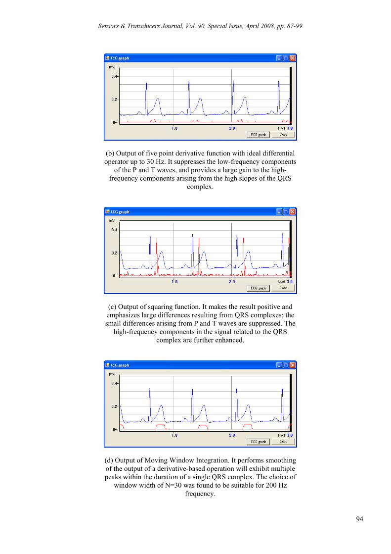
Sensors & Transducers Journal, Vol. 90, Special Issue, April 2008, pp. 87-99
94
(b) Output of five point derivative function with ideal differential operator up to 30 Hz. It suppresses the low-frequency components
of the P and T waves, and provides a large gain to the high-frequency components arising from the high slopes of the QRS
complex.
(c) Output of squaring function. It makes the result positive and emphasizes large differences resulting from QRS complexes; the small differences arising from P and T waves are suppressed. The
high-frequency components in the signal related to the QRS complex are further enhanced.
(d) Output of Moving Window Integration. It performs smoothing of the output of a derivative-based operation will exhibit multiple peaks within the duration of a single QRS complex. The choice of
window width of N=30 was found to be suitable for 200 Hz frequency.
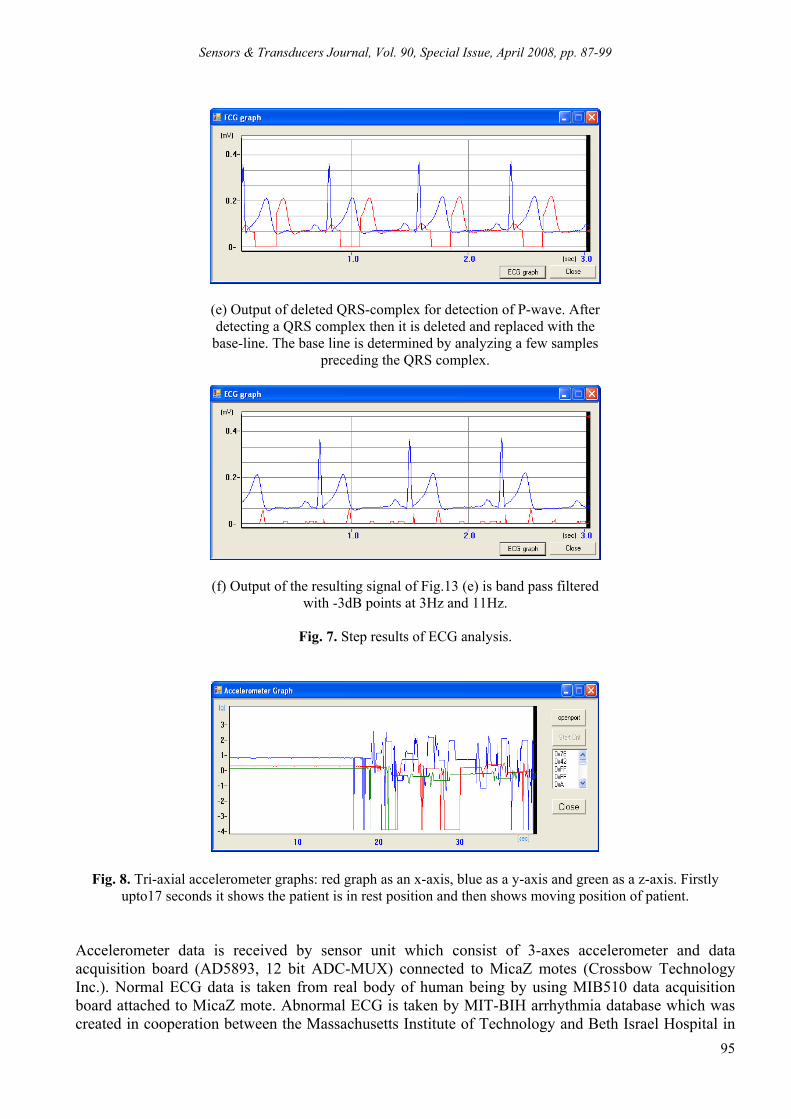
Sensors & Transducers Journal, Vol. 90, Special Issue, April 2008, pp. 87-99
95
(e) Output of deleted QRS-complex for detection of P-wave. After detecting a QRS complex then it is deleted and replaced with the base-line. The base line is determined by analyzing a few samples
preceding the QRS complex.
(f) Output of the resulting signal of Fig.13 (e) is band pass filtered with -3dB points at 3Hz and 11Hz.
Fig. 7. Step results of ECG analysis.
Fig. 8. Tri-axial accelerometer graphs: red graph as an x-axis, blue as a y-axis and green as a z-axis. Firstly upto17 seconds it shows the patient is in rest position and then shows moving position of patient.
Accelerometer data is received by sensor unit which consist of 3-axes accelerometer and data acquisition board (AD5893, 12 bit ADC-MUX) connected to MicaZ motes (Crossbow Technology Inc.). Normal ECG data is taken from real body of human being by using MIB510 data acquisition board attached to MicaZ mote. Abnormal ECG is taken by MIT-BIH arrhythmia database which was created in cooperation between the Massachusetts Institute of Technology and Beth Israel Hospital in
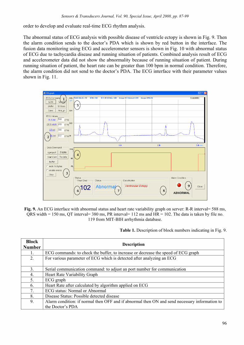
Sensors & Transducers Journal, Vol. 90, Special Issue, April 2008, pp. 87-99
96
order to develop and evaluate real-time ECG rhythm analysis. The abnormal status of ECG analysis with possible disease of ventricle ectopy is shown in Fig. 9. Then the alarm condition sends to the doctor’s PDA which is shown by red button in the interface. The fusion data monitoring using ECG and accelerometer sensors is shown in Fig. 10 with abnormal status of ECG due to tachycardia disease and running situation of patients. Combined analysis result of ECG and accelerometer data did not show the abnormality because of running situation of patient. During running situation of patient, the heart rate can be greater than 100 bpm in normal condition. Therefore, the alarm condition did not send to the doctor’s PDA. The ECG interface with their parameter values shown in Fig. 11.
Fig. 9. An ECG interface with abnormal status and heart rate variability graph on server: R-R interval= 588 ms, QRS width = 150 ms, QT interval= 380 ms, PR interval= 112 ms and HR = 102. The data is taken by file no.
119 from MIT-BIH arrhythmia database.
Table 1. Description of block numbers indicating in Fig. 9.
Block Number Description
1. ECG commands: to check the buffer, to increase or decrease the speed of ECG graph 2. For various parameter of ECG which is detected after analyzing an ECG
3. Serial communication command: to adjust an port number for communication 4. Heart Rate Variability Graph 5. ECG graph 6. Heart Rate after calculated by algorithm applied on ECG 7. ECG status: Normal or Abnormal 8. Disease Status: Possible detected disease 9. Alarm condition: if normal then OFF and if abnormal then ON and send necessary information to
the Doctor’s PDA

Sensors & Transducers Journal, Vol. 90, Special Issue, April 2008, pp. 87-99
97
Fig. 10. An ECG and Accelerometer interface with abnormal status on Server: R-R interval= 408 ms, QRS width = 68 ms, QT interval= 406 ms, PR interval = 112 ms, Resultant = 1.276345, Angle (degree) = 12.47328 and HR = 147. ECG data is taken by MIT-BIH arrhythmia
database and accelerometer data is received by sensor node attached to the human body.
Table 2. Description of block numbers indicating in Fig. 10.
Block Number Description
1. Tri-axial accelerometer graphs: Channel0 (x-axis)- Bule, Channel1 (y-axis) - Red, Channel2 (z-axis) - Green
2. ECG graph 3. Serial data receiving at server in packet format 4. Serial data receiving at server 5. ECG parameter values 6. Accelerometer parameter values 7. Heart Rate 8. Possible detected disease and status of patient for moving or rest or fall condition
9. Alarm condition: if normal then OFF and if abnormal then ON and send necessary information to the Doctor’s PDA
10. ECG and Accelerometer commands
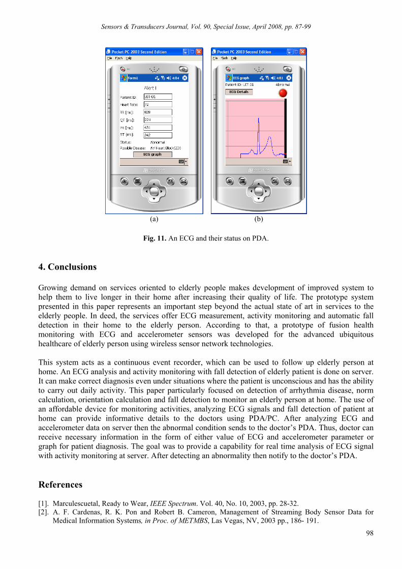
Sensors & Transducers Journal, Vol. 90, Special Issue, April 2008, pp. 87-99
98
(a) (b)
Fig. 11. An ECG and their status on PDA.
4. Conclusions Growing demand on services oriented to elderly people makes development of improved system to help them to live longer in their home after increasing their quality of life. The prototype system presented in this paper represents an important step beyond the actual state of art in services to the elderly people. In deed, the services offer ECG measurement, activity monitoring and automatic fall detection in their home to the elderly person. According to that, a prototype of fusion health monitoring with ECG and accelerometer sensors was developed for the advanced ubiquitous healthcare of elderly person using wireless sensor network technologies. This system acts as a continuous event recorder, which can be used to follow up elderly person at home. An ECG analysis and activity monitoring with fall detection of elderly patient is done on server. It can make correct diagnosis even under situations where the patient is unconscious and has the ability to carry out daily activity. This paper particularly focused on detection of arrhythmia disease, norm calculation, orientation calculation and fall detection to monitor an elderly person at home. The use of an affordable device for monitoring activities, analyzing ECG signals and fall detection of patient at home can provide informative details to the doctors using PDA/PC. After analyzing ECG and accelerometer data on server then the abnormal condition sends to the doctor’s PDA. Thus, doctor can receive necessary information in the form of either value of ECG and accelerometer parameter or graph for patient diagnosis. The goal was to provide a capability for real time analysis of ECG signal with activity monitoring at server. After detecting an abnormality then notify to the doctor’s PDA. References [1]. Marculescuetal, Ready to Wear, IEEE Spectrum. Vol. 40, No. 10, 2003, pp. 28-32. [2]. A. F. Cardenas, R. K. Pon and Robert B. Cameron, Management of Streaming Body Sensor Data for
Medical Information Systems, in Proc. of METMBS, Las Vegas, NV, 2003 pp., 186- 191.

Sensors & Transducers Journal, Vol. 90, Special Issue, April 2008, pp. 87-99
99
[3]. B. G. Cellar, N. H. Lovell and J. Basilakis, Using information technology to improve the management of chronic disease, Med. J. of Australia, 179, 5, 2003, pp. 242-246.
[4]. N. Maglaveras, I. Lekka et al., Congestive Heart Failure Management in a Home-Care System through the CHS Contact Center, IEEE Computers in Cardiology, Vol. 30, 2003, pp. 189-192.
[5]. M. H. Crawford, ACC/AHA Guidelines for ambulatory electrocardiography, Journal of the American College of Cardiology, Vol. 34, 1999, pp. 912-48.
[6]. J. Chen., K. Kwong, D. Chang, J. Luk, Ruzena Bajcsy, Wearable Sensors for Reliable Fall Detection, Proceedings of Engineering in Medicine and Biology, IEEE, Vol. 27, 2005, pp. 3551-3554.
[7]. D. M. Karantonis, M. R. Narayanan, M. Mathie, N. H. Lovell, and Branko G. Celler, Implementation of a Real-Time Human Movement Classifier Using a Triaxial Accelerometer for Ambulatory Monitoring, IEEE Transactions on Information Technology in Biomedicine, Vol. 10, No. 1, 2006, pp. 156-167.
[8]. R. Fensli, E. Gunnarson, and O. Hejlesen, A Wireless ECG System for Continuous Event Recording and Communication to a Clinical Alarm Station, 26th Annual International Conference of the IEEE Engineering in Medicine and Biology Society, 2004, pp. 2208-2211.
[9]. Sachin Bhardwaj, Dae-Seok Lee, S. C. Mukhopadhyay and Wan-Young Chung, A Fusion Data Monitoring of Multiple Wireless Sensors for Ubiquitous Healthcare System, 2nd International Conference on Sensing Technology, Palmerston North, New Zealand, 26-28, November 2007.
[10]. J. Pan and W. J. Tompkins, A real-time QRS detection algorithm, BME-32, pp. 230-236 1985. [11]. Hamilton P. S., Tompkins W. J., Quantitative investigation of QRS detection rules using the MIT/BIH
arrhythmia database, IEEE Trans. Biomed Eng., 1986, pp. 1157-65. [12]. Harvard-MIT Division of Health Sciences and Technology, WFDB Applications Guide,
http://www.physionet.org (visited on 14/7/2007).
___________________ 2008 Copyright ©, International Frequency Sensor Association (IFSA). All rights reserved. (http://www.sensorsportal.com)

Sensors & Transducers Journal, Vol. 90, Special Issue, April 2008, pp. 100-116
100
SSSeeennnsssooorrrsss &&& TTTrrraaannnsssddduuuccceeerrrsss
ISSN 1726-5479© 2008 by IFSA
http://www.sensorsportal.com
Resistive and Capacitive Based Sensing Technologies
1Winncy Y. Du and 2Scott W. Yelich 1San Jose State University, San Jose, USA
2S&W Consultants, Santa Clara, USA E-mail: [email protected], [email protected]
Received: 15 October 2007 /Accepted: 20 February 2008 /Published: 15 April 2008 Abstract: Resistive and capacitive (RC) sensors are the most commonly used sensors. Their applications span homeland security, industry, environment, space, traffic control, home automation, aviation, and medicine. More than 30% of modern sensors are direct or indirect applications of the RC sensing principles. This paper reviews resistive and capacitive sensing technologies. The physical principles of resistive sensors are governed by several important laws and phenomena such as Ohm’s Law, Wiedemann-Franz Law; Photoconductive-, Piezoresistive-, and Thermoresistive Effects. The applications of these principles are presented through a variety of examples including accelerometers, flame detectors, pressure/flow rate sensors, RTDs, hygristors, chemiresistors, and bio-impedance sensors. The capacitive sensors are described through their three configurations: parallel (flat), cylindrical (coaxial), and spherical (concentric). Each configuration is discussed with respect to its geometric structure, function, and application in various sensor designs. Capacitance sensor arrays are also presented in the paper. Copyright © 2008 IFSA. Keywords: Resistive sensors, Capacitive sensors, Sensor arrays, Sensor design 1. 1. Introduction This paper reviews the resistive and capacitive (RC) based measurement principles and their applications in sensing technologies. RC sensors apply a broad range of theories and phenomena from the fields of physics, material science, biology, electrochemistry, and electronics [1, 2]. Resistive sensors have assisted mankind in analyzing, controlling, and monitoring thousands of functions for over a century. Some milestones in the development of resistive sensors include the discovery of the Piezoresistive Effect by Lord Kelvin in 1856, the use of platinum as the element of a resistance thermometer by Sir William Siemens in 1871, the invention of a Carbon Track

Sensors & Transducers Journal, Vol. 90, Special Issue, April 2008, pp. 100-116
101
Potentiometer by Thomas Edison in 1872, and the patenting of a non-linear rheostat by Mary Hallock-Greenewalt in 1920. In automobiles, resistive sensors are used to measure air flow rate, throttle position, coolant/air temperature, oxygen volume, wheel speed, and so forth. In airplanes, highly reliable resistive sensors monitor engine functions, hydraulic systems, electronic devices, temperature and pressure readings, and have greatly increased aircraft safety. Measuring and analyzing electrical impedance characteristics of the human body have allowed doctors to diagnose certain diseases, monitor health conditions, and analyze the treatment results. The advantages of resistive sensors are their reliability, simple construction, adjustable resolution, and maintenance-free technology. Electrical resistance is also the easiest electrical property to measure precisely over a wide range at moderate cost. These important features have often made resistive sensors the preferred choice in sensor designs. Capacitive sensors are traditionally divided into two basic classifications: passive or active, based on whether or not there are any electronic components in the sensor. Passive sensors do not have any electronics in the sensor, thus minimizing guard size. Passive sensors have some significant advantages: they have greater flexibility in probe configuration, are more stable, and cost less than active systems. Their disadvantages include lower bandwidth and lower drive frequency, which makes them unsuitable for some applications. Active sensors have electronics, usually a small circuit board, packaged inside the sensors. Active sensors operate at much higher frequencies and bandwidths, and are particularly well suited to applications which may involve stray electrical noise on the target. Their disadvantages include higher costs and less configuration flexibility [3]. Capacitive sensors are the most precise of all electrical sensors and are known for their extremely high sensitivity, high resolution, high bandwidth, robustness, stability, and drift-free measurement capability. Capacitive sensors can be used in a wide range of applications including: precision movement detection, coating thickness gauging, liquid level and flow rate monitoring, diamond turning, chemical element selection, biocell recognition, and aircraft engine rotational alignment. They can also be used in severe environments (high temperature, magnetic fields, and radiation) and in non-contact and non-intrusive applications. The progress in micro- and nano-machining technologies have significantly advanced traditional resistive and capacitive transducers to a new level – high sensitivity, low power consumption, rapid response time, and miniaturization. Resistance and capacitance sensing principles can also be combined with other sensing technologies, such as ultrasonic, RF, CMOS, or fiber-optics, to create more sophisticated and powerful hybrid sensors. This paper is organized as follows: Section 1 is an introduction; Section 2 overviews the principles, design, and application of resistive sensors; Section 3 presents the classification, principles, design, and application of capacitive sensors; and Section 4 gives the summary. 2. Resistive Sensing Technologies 2.1. Principles Resistive sensors are used to monitor physical or chemical parameters that can induce a change in electrical resistance. The magnitude of the physical or chemical parameter, such as light, strain, voltage, magnetic field, or gas/liquid concentration, can be inferred from the measured resistance value. The basic physical principles behind resistive sensors are summarized in Table 2.1.

Sensors & Transducers Journal, Vol. 90, Special Issue, April 2008, pp. 100-116
102
Table 2.1. Basic Physical Principles of Resistive Sensors.
Ohm’s Law: The resistivity R (or conductivity 1/R) of a material passing electric current I under an applied voltage V is:
IVR = (2.1)
The electrical resistance is a function of both its physical geometry and the resistivity of the material:
alR ρ= (2.2)
l – length; ρ – specific resistivity of the material; a – cross sectional area.
Photoconductive Effect: When light strikes certain materials, the resistance of the material decreases. For instance, the conductance of a semiconductor is described by:
)( ppnnen τµτµσ +=∆ (2.3)
µn, µp – free-electron and hole movement; τn, τp – free-electron and hole lives; e – charge of an electron; n – number of generated carriers per second per unit of volume.
Piezoresistive Effect: Resistance changes when the material is mechanically deformed. The sensitivity of resistance with respect to wire elongation dl is:
lvdl
dR ρ2= (2.4)
ρ – specific resistivity of the material; l – conductor’s length before deformation; v – volume of the material.
Wiedemann-Franz Law: The ratio of the thermal conductivity to the electrical conductivity of a material is proportional to its absolute temperature.
LTK =σ/ (2.5)K – thermal conductivity; σ – electrical conductivity; L – proportionality constant (Lorenz Number); T – absolute temperature.
Thermoresistive Effect of Metals: The electrical resistance of a metal conductor increases as the temperature increases. The relationship between temperature and resistance is:
( ) ( ) ( )[ ]...1)( 30
2000 +−+−+−+= ttttttRtR γβα
A simplified version of the above equation is: ( )[ ]00 1)( ttRtR −+= α (2.6)
R0 – resistance at the reference temperature t0 (usually either 0oC or 25oC); α, β, γ – temperature coefficients.
Thermoresistive Effect of Semiconductor Materials: Electrical resistance of semiconductor materials decreases with increasing temperature. The relationship between electrical resistance and temperature is exponential:
⎥⎥⎦
⎤
⎢⎢⎣
⎡⎟⎟⎠
⎞⎜⎜⎝
⎛−
= 0
11
0)( tteRtRβ
(2.7) R0 – resistance at the reference temperature t0 (usually either 0oC or 25oC); β – temperature coefficient.
Bioimpedance Model: Electrical properties of the human body can be characterized by a three-element equivalent electrical model as shown in the Figure. Impedance of the human body Z is [4]:
)1//()//( ieice RCj
RRZRZ +=+=ω
(2.8)
2.2. Design and Applications Potentiometric Sensors A potentiometer (or pot) relates a change in length to a resistance change. The resistance of a pot can be varied by the position of a movable contact on a fixed resistor, which can be either linear or circular in shape. Pots are commonly used as a linear or angular position sensor, air flow meter, wind direction detector, or volume and tone control in stereo equipment. Fig. 2.1 shows a potentiometric type of pressure sensor designed by SFIM SAGEM, France. It has three terminals: a power input, a ground and a variable voltage output. When the pressure of an input liquid or gas expands the diaphragm, the wiper connected to the diaphragm will slide along the potentiometer. The location of the wiper is determined by the magnitude of the pressure.
Ri C
Re
Re: extracellular liquid resistance Ri: intracellular liquid resistance C: cell membrane capacitance
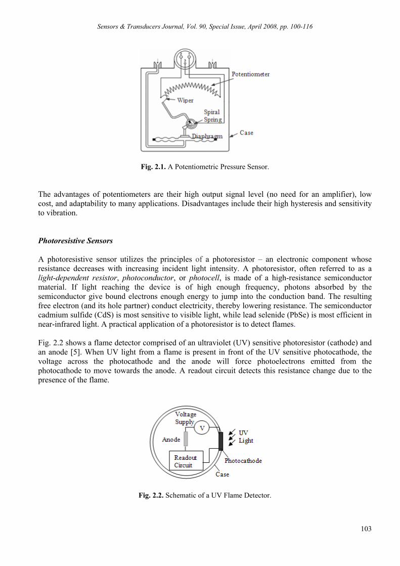
Sensors & Transducers Journal, Vol. 90, Special Issue, April 2008, pp. 100-116
103
Fig. 2.1. A Potentiometric Pressure Sensor.
The advantages of potentiometers are their high output signal level (no need for an amplifier), low cost, and adaptability to many applications. Disadvantages include their high hysteresis and sensitivity to vibration. Photoresistive Sensors A photoresistive sensor utilizes the principles of a photoresistor – an electronic component whose resistance decreases with increasing incident light intensity. A photoresistor, often referred to as a light-dependent resistor, photoconductor, or photocell, is made of a high-resistance semiconductor material. If light reaching the device is of high enough frequency, photons absorbed by the semiconductor give bound electrons enough energy to jump into the conduction band. The resulting free electron (and its hole partner) conduct electricity, thereby lowering resistance. The semiconductor cadmium sulfide (CdS) is most sensitive to visible light, while lead selenide (PbSe) is most efficient in near-infrared light. A practical application of a photoresistor is to detect flames. Fig. 2.2 shows a flame detector comprised of an ultraviolet (UV) sensitive photoresistor (cathode) and an anode [5]. When UV light from a flame is present in front of the UV sensitive photocathode, the voltage across the photocathode and the anode will force photoelectrons emitted from the photocathode to move towards the anode. A readout circuit detects this resistance change due to the presence of the flame.
Fig. 2.2. Schematic of a UV Flame Detector.

Sensors & Transducers Journal, Vol. 90, Special Issue, April 2008, pp. 100-116
104
Photoresistors are generally inexpensive. Their small size and ease of use make them popular in many applications, e.g., detecting fires, turning street lights on and off automatically according to the level of daylight, reading inventory bar codes, sensing motion, and measuring light intensity. Piezoresistive Sensors Piezoresistive sensors are designed based on a materials’ piezoresistivity – defined as a change in electrical resistance of the material due to its mechanical deformation. Piezoresistive sensors are commonly used to measure force, pressure, acceleration, vibration, and impact. Piezoresistive accelerometers have an advantage over piezoelectric accelerometers in that they can measure accelerations down to zero Hz. They have good high frequency response with relatively low voltage output and high performance. However, their output signals are easily affected by temperature variations and noise, thus compensation circuits are often required to correct sensor errors. Fig. 2.3 illustrates a catheter based medical device for intravascular blood pressure measurement [6]. Its diaphragm consists of a force transducing beam and a piezoresistor. The sensor chip is ultra-miniaturized (0.1mmx0.14mmx1.3mm).
Fig. 2.3. A Piezoresistive Blood Pressure Sensor.
Thermoresistive Sensors Resistance-based temperature sensing devices include Resistance Temperature Detectors (RTDs) and Thermistors. RTDs are positive temperature coefficient sensors whose resistance increases with temperature. RTDs are constructed in wire-wound and thin film types (Fig. 2.4). The former is made by winding a very fine metal wire around an inert substrate (glass or ceramic). The latter is produced through Thin Film Technology or Thin Film Lithography that deposits a thin film of metal (e.g., 1 µm Platinum) onto a ceramic substrate through cathodic atomization or “sputtering”.
Fig. 2.4. Two Types of RTD Construction [7].
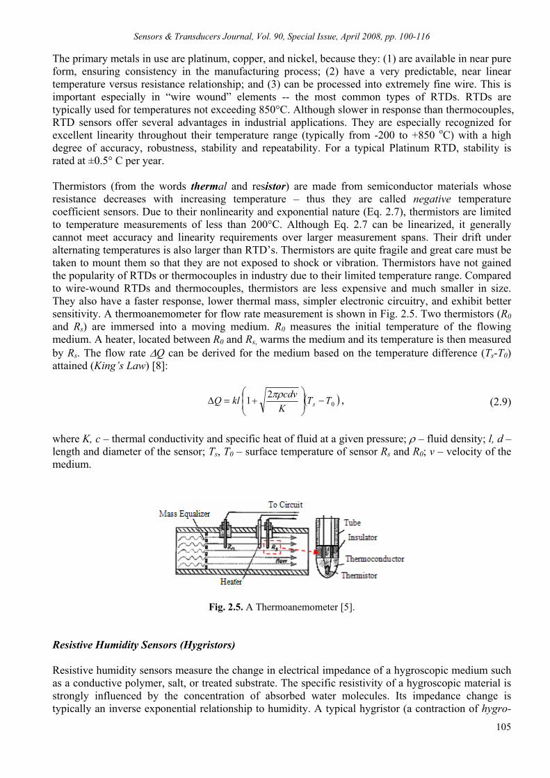
Sensors & Transducers Journal, Vol. 90, Special Issue, April 2008, pp. 100-116
105
The primary metals in use are platinum, copper, and nickel, because they: (1) are available in near pure form, ensuring consistency in the manufacturing process; (2) have a very predictable, near linear temperature versus resistance relationship; and (3) can be processed into extremely fine wire. This is important especially in “wire wound” elements -- the most common types of RTDs. RTDs are typically used for temperatures not exceeding 850°C. Although slower in response than thermocouples, RTD sensors offer several advantages in industrial applications. They are especially recognized for excellent linearity throughout their temperature range (typically from -200 to +850 oC) with a high degree of accuracy, robustness, stability and repeatability. For a typical Platinum RTD, stability is rated at ±0.5° C per year. Thermistors (from the words thermal and resistor) are made from semiconductor materials whose resistance decreases with increasing temperature – thus they are called negative temperature coefficient sensors. Due to their nonlinearity and exponential nature (Eq. 2.7), thermistors are limited to temperature measurements of less than 200°C. Although Eq. 2.7 can be linearized, it generally cannot meet accuracy and linearity requirements over larger measurement spans. Their drift under alternating temperatures is also larger than RTD’s. Thermistors are quite fragile and great care must be taken to mount them so that they are not exposed to shock or vibration. Thermistors have not gained the popularity of RTDs or thermocouples in industry due to their limited temperature range. Compared to wire-wound RTDs and thermocouples, thermistors are less expensive and much smaller in size. They also have a faster response, lower thermal mass, simpler electronic circuitry, and exhibit better sensitivity. A thermoanemometer for flow rate measurement is shown in Fig. 2.5. Two thermistors (R0 and Rs) are immersed into a moving medium. R0 measures the initial temperature of the flowing medium. A heater, located between R0 and Rs, warms the medium and its temperature is then measured by Rs. The flow rate ∆Q can be derived for the medium based on the temperature difference (Ts-T0) attained (King’s Law) [8]:
( )021 TT
KcdvklQ s −⎟
⎟⎠
⎞⎜⎜⎝
⎛+=∆
πρ , (2.9)
where K, c – thermal conductivity and specific heat of fluid at a given pressure; ρ – fluid density; l, d – length and diameter of the sensor; Ts, T0 – surface temperature of sensor Rs and R0; v – velocity of the medium.
Fig. 2.5. A Thermoanemometer [5].
Resistive Humidity Sensors (Hygristors) Resistive humidity sensors measure the change in electrical impedance of a hygroscopic medium such as a conductive polymer, salt, or treated substrate. The specific resistivity of a hygroscopic material is strongly influenced by the concentration of absorbed water molecules. Its impedance change is typically an inverse exponential relationship to humidity. A typical hygristor (a contraction of hygro-
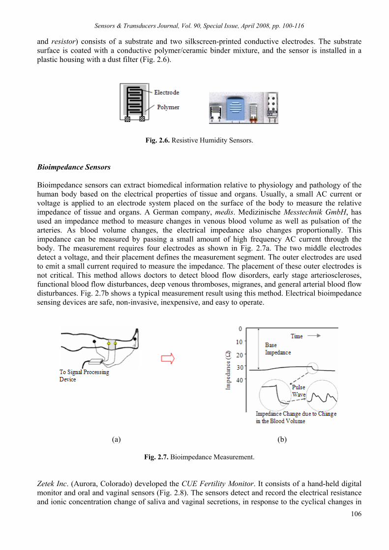
Sensors & Transducers Journal, Vol. 90, Special Issue, April 2008, pp. 100-116
106
and resistor) consists of a substrate and two silkscreen-printed conductive electrodes. The substrate surface is coated with a conductive polymer/ceramic binder mixture, and the sensor is installed in a plastic housing with a dust filter (Fig. 2.6).
Fig. 2.6. Resistive Humidity Sensors.
Bioimpedance Sensors Bioimpedance sensors can extract biomedical information relative to physiology and pathology of the human body based on the electrical properties of tissue and organs. Usually, a small AC current or voltage is applied to an electrode system placed on the surface of the body to measure the relative impedance of tissue and organs. A German company, medis. Medizinische Messtechnik GmbH, has used an impedance method to measure changes in venous blood volume as well as pulsation of the arteries. As blood volume changes, the electrical impedance also changes proportionally. This impedance can be measured by passing a small amount of high frequency AC current through the body. The measurement requires four electrodes as shown in Fig. 2.7a. The two middle electrodes detect a voltage, and their placement defines the measurement segment. The outer electrodes are used to emit a small current required to measure the impedance. The placement of these outer electrodes is not critical. This method allows doctors to detect blood flow disorders, early stage arterioscleroses, functional blood flow disturbances, deep venous thromboses, migranes, and general arterial blood flow disturbances. Fig. 2.7b shows a typical measurement result using this method. Electrical bioimpedance sensing devices are safe, non-invasive, inexpensive, and easy to operate.
(a)
(b)
Fig. 2.7. Bioimpedance Measurement.
Zetek Inc. (Aurora, Colorado) developed the CUE Fertility Monitor. It consists of a hand-held digital monitor and oral and vaginal sensors (Fig. 2.8). The sensors detect and record the electrical resistance and ionic concentration change of saliva and vaginal secretions, in response to the cyclical changes in
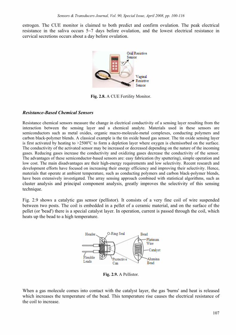
Sensors & Transducers Journal, Vol. 90, Special Issue, April 2008, pp. 100-116
107
estrogen. The CUE monitor is claimed to both predict and confirm ovulation. The peak electrical resistance in the saliva occurs 5~7 days before ovulation, and the lowest electrical resistance in cervical secretions occurs about a day before ovulation.
Fig. 2.8. A CUE Fertility Monitor. Resistance-Based Chemical Sensors Resistance chemical sensors measure the change in electrical conductivity of a sensing layer resulting from the interaction between the sensing layer and a chemical analyte. Materials used in these sensors are semiconductors such as metal oxides, organic macro-molecule-metal complexes, conducting polymers and carbon black-polymer blends. A classical example is the tin oxide based gas sensor. The tin oxide sensing layer is first activated by heating to >2500oC to form a depletion layer where oxygen is chemisorbed on the surface. The conductivity of the activated sensor may be increased or decreased depending on the nature of the incoming gases. Reducing gases increase the conductivity and oxidizing gases decrease the conductivity of the sensor. The advantages of these semiconductor-based sensors are: easy fabrication (by sputtering), simple operation and low cost. The main disadvantages are their high-energy requirements and low selectivity. Recent research and development efforts have focused on increasing their energy efficiency and improving their selectivity. Hence, materials that operate at ambient temperature, such as conducting polymers and carbon black-polymer blends, have been extensively investigated. The array sensing approach combined with statistical algorithms, such as cluster analysis and principal component analysis, greatly improves the selectivity of this sensing technique. Fig. 2.9 shows a catalytic gas sensor (pellistor). It consists of a very fine coil of wire suspended between two posts. The coil is embedded in a pellet of a ceramic material, and on the surface of the pellet (or 'bead') there is a special catalyst layer. In operation, current is passed through the coil, which heats up the bead to a high temperature.
Fig. 2.9. A Pellistor.
When a gas molecule comes into contact with the catalyst layer, the gas 'burns' and heat is released which increases the temperature of the bead. This temperature rise causes the electrical resistance of the coil to increase.

Sensors & Transducers Journal, Vol. 90, Special Issue, April 2008, pp. 100-116
108
A more versatile sensing system is based on the carbon black-polymer blend where the carbon particles give the electrical conductivity and the polymer provides the sensor function. The sensor response is a result of the polymer swelling, which causes the conductivity of the sensor to change. The main advantages of using carbon black-polymer blends as a sensing layer are that the sensor is reusable and the selectivity can be tailored by choosing polymers with desired functionalities. Fig. 2.10 shows a chemiresistor formed by depositing a thin film of non-conductive polymer, infused with carbon black particles, onto the metallic inter-digitated electrodes of a glass chip. The absorption of certain chemical vapor results in a measurable decrease in the electrical conductance of the sensing element. Such sensors are inexpensive and easily mass-produced. A potential commercial application for this sensing technique could be a system for detecting illegal drugs [9].
Fig. 2.10. Operation of a Chemiresistor.
3. Capacitive Sensing Technologies 3.1. Types of Capacitive Sensors At the heart of any capacitive-sensing system is a capacitor. Capacitors are available in three configurations: flat (parallel), cylindrical (coaxial), and spherical (concentric), as shown in Table 3.1. All capacitive sensors fall into one of these three design classifications, with the flat and cylindrical being the most commonly used forms.
Table 3.1. Capacitance & Capacitor Configurations.
In the table, εr is the relative permittivity of the medium between the electrodes: ε0 is the permittivity of a vacuum. The ratios A/d, 2πl/[ln(r2/r1)], or 4πr1r2/(r2-r1) are the geometry factors for a parallel-plate capacitor, a coaxial capacitor, and a spherical capacitor respectively. Eqs. 3.1-3.3 describe the relationship between capacitance and the dielectric constants (εr, ε0) as well as the geometric parameters (A, d, l, r1, r2). Varying any of these components will change the capacitance, which then can be accurately measured and thus defines the operating principle of capacitive sensors. Advantages of capacitive sensors are their simple structures, high sensitivity, high resolution, temperature resistance, long-term stability, and durability. Some capacitive sensors can achieve sub-nanometer position resolution (<0.01nm), having a bandwidth to 100 kHz. Capacitive sensors can provide contact

Sensors & Transducers Journal, Vol. 90, Special Issue, April 2008, pp. 100-116
109
or noncontact measurement of various physical or chemical quantities representing distance, position, acceleration, separation, proximity, force, pressure, biocells, chemical substances, and particles. 3.2. Design and Applications Parallel Capacitor-based Sensors The majority of capacitive sensors use the parallel-plate configuration. The sensing principle of such sensors is based on a capacitance change due to a change in one or more of the following (refer to Fig. 3.1): (1) the distance between two plates; (2) the area of overlap between two plates; (3) the dielectric constant; (4) the conductivity of the plate(s).
Fig. 3.1. Capacitance Varies with Distance, Area, Dielectric Constant, and Electrode Conductivity.
Parallel capacitive sensors are either single or dual-plate design. In a single plate (or electrode) design, the target – a conductive object, functions as the second electrode (Fig. 3.2a); while in the dual-plate design (Fig. 3.2b), the target – a non-conductive (or very low conductivity) object, serves to vary the amount of electric flux reaching the second electrode.
Fig. 3.2. Single-Electrode and Dual-Electrode Design.
Parallel capacitive sensors can detect motion, distance, acceleration, fluid level, biocells, and chemicals. Some of these applications are summarized in Table 3.2. Parallel capacitive sensors can also be designed to measure pressure; such sensors are relatively robust compared to other types of pressure sensors. A capacitance variation can be obtained when a pressure acts on one of the parameters modifying the electric field between two electrodes of a capacitor. Fig. 3.3a shows a capacitive pressure sensor (VEGA Technique, France). One of its electrodes is connected to a sensing diaphragm. The unit forms a capacitor whose variation in capacitance is determined by the displacement of the diaphragm. In this case, the variable parameter of capacitance C is the surface area A of the plates, and A itself is a linear function of the displacement l. An alternative design of a pressure sensor is to measure the variation of distance d between two plates (see Fig. 3.3b).

Sensors & Transducers Journal, Vol. 90, Special Issue, April 2008, pp. 100-116
110
Table 3.2. Applications of Parallel Capacitive Sensors.
Fig. 3.3. Capacitive Pressure Sensors: (a) with A Variation; (b) with d Variation.
If one plate of a parallel capacitor moves with respect to acceleration or vibration, a capacitive accelerometer is formed. Fig. 3.4a shows a PCB Piezotronics capacitive accelerometer. It contains a diaphragm, which acts as a mass undergoing flexure in the presence of acceleration. Two plates sandwich the diaphragm, creating two capacitors, each with an individual fixed plate and each sharing the diaphragm as a movable plate. The flexure causes a capacitance shift by altering the distance between the two parallel plates. The two capacitance values are sent to a bridge circuit, and the electrical output varies with input acceleration. Such a design can achieve true DC response and high performance for uniform acceleration and low-frequency vibration measurement as shown in Fig. 3.4b.
(a)
(b)
Fig. 3.4. Typical Element Structure of a Capacitive Accelerometer (a) and its Response (b).
Capacitive sensor designs based on variation of the dielectric constant are often found in humidity, force/pressure, chemical-substance, and biocell sensing applications. Fig. 3.5 illustrates the mechanism of a pellicular sensor developed by ONERA French Aerospace Lab. The sensor detects a change in relative permittivity of the dielectric εr between two electrodes when a force or pressure is exerted on
Dust Sensing
Dust
Coating Thickness Sensing
Force MeasurementVibration Sensing
Out-of-Plane, Out-of-Round Measurement
Displacement Sensing
Tip/Tilt MeasurementFlatness & Straightness Sensing
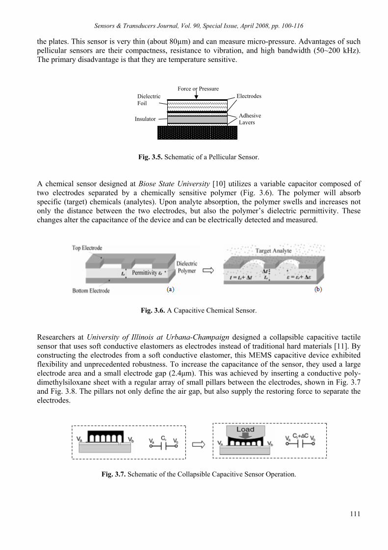
Sensors & Transducers Journal, Vol. 90, Special Issue, April 2008, pp. 100-116
111
the plates. This sensor is very thin (about 80µm) and can measure micro-pressure. Advantages of such pellicular sensors are their compactness, resistance to vibration, and high bandwidth (50~200 kHz). The primary disadvantage is that they are temperature sensitive.
Fig. 3.5. Schematic of a Pellicular Sensor.
A chemical sensor designed at Biose State University [10] utilizes a variable capacitor composed of two electrodes separated by a chemically sensitive polymer (Fig. 3.6). The polymer will absorb specific (target) chemicals (analytes). Upon analyte absorption, the polymer swells and increases not only the distance between the two electrodes, but also the polymer’s dielectric permittivity. These changes alter the capacitance of the device and can be electrically detected and measured.
Fig. 3.6. A Capacitive Chemical Sensor.
Researchers at University of Illinois at Urbana-Champaign designed a collapsible capacitive tactile sensor that uses soft conductive elastomers as electrodes instead of traditional hard materials [11]. By constructing the electrodes from a soft conductive elastomer, this MEMS capacitive device exhibited flexibility and unprecedented robustness. To increase the capacitance of the sensor, they used a large electrode area and a small electrode gap (2.4µm). This was achieved by inserting a conductive poly-dimethylsiloxane sheet with a regular array of small pillars between the electrodes, shown in Fig. 3.7 and Fig. 3.8. The pillars not only define the air gap, but also supply the restoring force to separate the electrodes.
Fig. 3.7. Schematic of the Collapsible Capacitive Sensor Operation.
Force or Pressure Electrodes Dielectric
Foil
Adhesive LayersInsulator

Sensors & Transducers Journal, Vol. 90, Special Issue, April 2008, pp. 100-116
112
Fig. 3.8. (a) Flexible Conductor Capacitive Tactile Sensor; (b) Micrograph of Support Pillar Array Built into Flexible Conductor.
Well-designed electrodes of capacitive sensors also allow scientists and researchers to analyze deoxyribonucleic acid (DNA) for applications in medicine and biology. A label-free capacitive DNA sensing algorithm has been developed at University of Bologna in Italy [12]. In this method the electrode-solution interfaces are characterized by capacitive parameters sensitive to the state of the electrode surface. DNA targets in the solution bond with the probe and affect the value of interface electrical capacitance, this variation is then measured by accurate instruments. Advantages of this method over the conventional optical marker are: (1) no need for an expensive optical reading device; (2) real-time detection; and (3) improved sensitivity. Coaxial Capacitor-based Sensors The coaxial configuration is the second most popular design in capacitive sensors. A simple displacement sensor can be easily built using a cylindrical capacitor if the inner conductor can be moved in and out of the outer conductor (Fig. 3.9). According to Eq. (3.2), the capacitance of such a sensor is in a linear relationship with the displacement l.
Fig. 3.9. A Capacitive Displacement Sensor.
Coaxial capacitors are commonly used for fluid level measurement. There are two designs: one for fluids with low dielectric constants (or high conductivity, see Fig. 3.10a), and another for fluids with high dielectric constants (or low conductivity, see Fig. 3.10b). In Design (a), the surface of the metal electrode is coated with a thin isolating layer (e.g., Teflon or Kynar) to prevent an electric short circuit through the liquid. The insulated probe acts as one plate of the capacitor and the conductive liquid acts as the other, and it is electrically connected to the ground. The insulating or dielectric medium in this case is the probe’s sheath. In Design (b), a bare rod and the metallic vessel wall form the electrodes of a capacitor; the dielectric medium is the liquid. The vessel wall (or reference probe) is grounded in this case. Usually, a potentiometer is built in so that liquids with different densities and different dielectric constants can be measured. A bridge circuit measures the capacitance and provides continuous liquid level monitoring.
(b)
(a)

Sensors & Transducers Journal, Vol. 90, Special Issue, April 2008, pp. 100-116
113
(a)
(b)
Fig. 3.10. Capacitive Liquid Level Sensors.
The cross section of a capacitive touch transducer is shown in Fig. 3.11. This sensor uses a coaxial capacitor design and a high dielectric polymer (e.g., polyvinylidene fluoride) to maximize the change in capacitance as force is applied. The movement of one set of the capacitor’s plates is used to resolve the displacement and hence applied force, which causes a capacitance change. From an application viewpoint, the coaxial design is better than a flat plate design as it will give a greater capacitance increase for an applied force.
Fig. 3.11. Schematic of a Coaxial Capacitor Touch Sensor.
Euro Gulf Group Company has developed an Oil Analyzer (EASZ-1), which uses the capacitance principle to measure moisture content in oil (see Fig. 3.12a and b). The cylindrical sensor and outer barrel are fixed in size and distance from each other and form the electrodes of a coaxial capacitor. The oil sample flows between the "plates" as a dielectric fluid, changing the capacitance of the assembly proportionally with the change in dielectric constant of the fluid. The measured capacitance is then converted to a water content output signal by the microprocessor and associated components to deliver stable and accurate readings. There is also a built-in temperature sensor for temperature compensation.
(a)
(b)
Fig. 3.12. EASZ-1 Analyzer (a) and its Typical Installation on a Hydraulic Line (b).
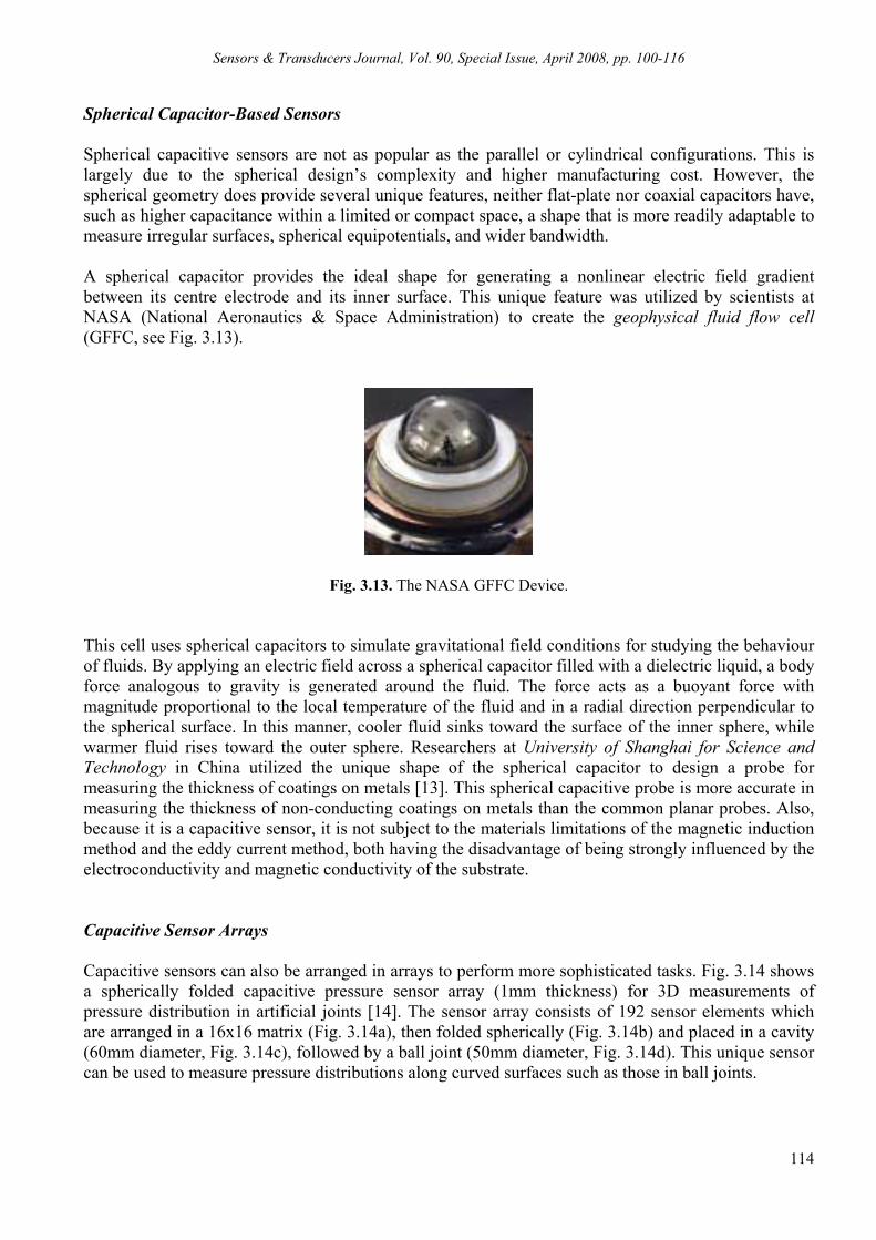
Sensors & Transducers Journal, Vol. 90, Special Issue, April 2008, pp. 100-116
114
Spherical Capacitor-Based Sensors Spherical capacitive sensors are not as popular as the parallel or cylindrical configurations. This is largely due to the spherical design’s complexity and higher manufacturing cost. However, the spherical geometry does provide several unique features, neither flat-plate nor coaxial capacitors have, such as higher capacitance within a limited or compact space, a shape that is more readily adaptable to measure irregular surfaces, spherical equipotentials, and wider bandwidth. A spherical capacitor provides the ideal shape for generating a nonlinear electric field gradient between its centre electrode and its inner surface. This unique feature was utilized by scientists at NASA (National Aeronautics & Space Administration) to create the geophysical fluid flow cell (GFFC, see Fig. 3.13).
Fig. 3.13. The NASA GFFC Device.
This cell uses spherical capacitors to simulate gravitational field conditions for studying the behaviour of fluids. By applying an electric field across a spherical capacitor filled with a dielectric liquid, a body force analogous to gravity is generated around the fluid. The force acts as a buoyant force with magnitude proportional to the local temperature of the fluid and in a radial direction perpendicular to the spherical surface. In this manner, cooler fluid sinks toward the surface of the inner sphere, while warmer fluid rises toward the outer sphere. Researchers at University of Shanghai for Science and Technology in China utilized the unique shape of the spherical capacitor to design a probe for measuring the thickness of coatings on metals [13]. This spherical capacitive probe is more accurate in measuring the thickness of non-conducting coatings on metals than the common planar probes. Also, because it is a capacitive sensor, it is not subject to the materials limitations of the magnetic induction method and the eddy current method, both having the disadvantage of being strongly influenced by the electroconductivity and magnetic conductivity of the substrate. Capacitive Sensor Arrays Capacitive sensors can also be arranged in arrays to perform more sophisticated tasks. Fig. 3.14 shows a spherically folded capacitive pressure sensor array (1mm thickness) for 3D measurements of pressure distribution in artificial joints [14]. The sensor array consists of 192 sensor elements which are arranged in a 16x16 matrix (Fig. 3.14a), then folded spherically (Fig. 3.14b) and placed in a cavity (60mm diameter, Fig. 3.14c), followed by a ball joint (50mm diameter, Fig. 3.14d). This unique sensor can be used to measure pressure distributions along curved surfaces such as those in ball joints.
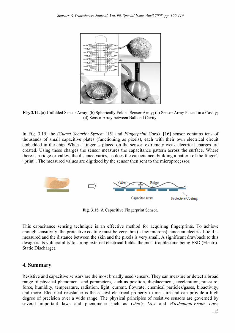
Sensors & Transducers Journal, Vol. 90, Special Issue, April 2008, pp. 100-116
115
Fig. 3.14. (a) Unfolded Sensor Array; (b) Spherically Folded Sensor Array; (c) Sensor Array Placed in a Cavity;
(d) Sensor Array between Ball and Cavity.
In Fig. 3.15, the iGuard Security System [15] and Fingerprint Cards' [16] sensor contains tens of thousands of small capacitive plates (functioning as pixels), each with their own electrical circuit embedded in the chip. When a finger is placed on the sensor, extremely weak electrical charges are created. Using these charges the sensor measures the capacitance pattern across the surface. Where there is a ridge or valley, the distance varies, as does the capacitance; building a pattern of the finger's “print”. The measured values are digitized by the sensor then sent to the microprocessor.
Fig. 3.15. A Capacitive Fingerprint Sensor.
This capacitance sensing technique is an effective method for acquiring fingerprints. To achieve enough sensitivity, the protective coating must be very thin (a few microns), since an electrical field is measured and the distance between the skin and the pixels is very small. A significant drawback to this design is its vulnerability to strong external electrical fields, the most troublesome being ESD (Electro-Static Discharge). 4. Summary Resistive and capacitive sensors are the most broadly used sensors. They can measure or detect a broad range of physical phenomena and parameters, such as position, displacement, acceleration, pressure, force, humidity, temperature, radiation, light, current, flowrate, chemical particles/gases, bioactivity, and more. Electrical resistance is the easiest electrical property to measure and can provide a high degree of precision over a wide range. The physical principles of resistive sensors are governed by several important laws and phenomena such as Ohm’s Law and Wiedemann-Franz Law;

Sensors & Transducers Journal, Vol. 90, Special Issue, April 2008, pp. 100-116
116
Photoconductive-, Piezoresistive-, and Thermoresistive Effects, which relate electrical resistance values to the magnitude of the physical or chemical parameters. The operating principles of capacitive sensors are based on the properties of a capacitor: capacitance variation is a function of changes in dielectric constant, materials, electrode conductivity, and geometric parameters. Each capacitive sensor is designed to measure one or more of these parameters. All capacitive sensors fall into one of the three basic capacitor configurations: flat-plate, coaxial, or spherical, depending on their intended use and function. Several typical sensor designs and applications in each configuration, as well as sensor arrays, are described in the paper. References [1]. W. Du., S. Yelich, Resistive Sensors: Principles, Design, and Applications, Proceedings of the 2nd
International Conference on Sensing Technology, Nov. 26-28, 2007, Palmerston North, New Zealand, pp. 326-331.
[2]. W. Du., S. Yelich, Capacitive Sensors: Principles, Design, and Applications, Proceedings of the 2nd International Conference on Sensing Technology, Nov. 26-28, 2007, Palmerston North, New Zealand, pp. 332-337.
[3]. Introduction to Capacitance Gages, ADE Technologies, p. 6. [4]. H. P. Schwan, The Bioimpedance Field: Some Historical Observations, Proceedings of 9th ICEBI,
Heidelberg, Germany, 1995. [5]. J. Fraden, Handbook of Modern Sensors: Physics, Designs, and Applications, Springer-Verlag, 2003. [6]. E. Källvesten, P. Melvas, J. Melin, T. Frisk, G. Stemme, Ultra-miniaturized Pressure Sensors for
Intravascular Blood Pressure Measurements, KTH Royal Inst. of Tech., Sweden. [7]. T. Montgomery, Industrial Temperature Primer, Wilkerson Instrument Co. , 2007, p. 11. [8]. L. V. King, On the Convention of Heat from Small Cylinders in a Stream of Fluid, Phil. Trans. Roy. Soc.,
A214, 1914, p. 373. [9]. G. Man, A. Navabi, T. Raymond, B. Stoeber, K. Walus, Polymer-based Chemical Sensors for Clandestine
Lab Detection, CMC Workshop on MEMS & Microfluidics, Montreal, Canada, 2007. [10]. T. J. Plum, V. Saxena, and J.R. Jessing, Design of a MEMS Capacitive Chemical Sensor Based on Polymer
Swelling, IEEE WMED 2006. [11]. J. Engel, J. Chen, N. Chen, S. Pandya, and C. Liu, Multi-Walled Carbon Nanotube Filled Conductive
Elastomers: Materials & Application to Micro Transducers, 19th IEEE International Conference on Micro Electro Mechanical Systems, Istanbul, Turkey, Jan. 22-26, 2006, pp. 246-249.
[12]. C. Guiducci, C. Stagni, A. Fischetti, U. Mastro-matter, Microelectrodes on a Silicon Chip for Label-free Capacitive DNA Sensing, Sensor Journal, Vol. 6, No. 5, 2006, pp. 1084-1093.
[13]. R. Zhang, S. Dai, and P Mu, A Spherical Capacitive Probe for Measuring the Thickness of Coatings on Metals, Measurement Science Technology, 8, 1997, pp. 1028–1033. (Printed in the UK).
[14]. O. Muller, W. J. Parak, M. G. Wiedemann, and F. Martini, Three-Dimensional Measurements of the Pressure Distribution in Artificial Joints with A Capacitive Sensor Array, Journal of Biomechanics, 37, 2004, 1623–1625.
[15]. Solid-state, Silicon-based Capacitive Fingerprint Sensor, Retrieved on Jan. 20, 2008 at www.iguardsystem.com.
[16]. Fingerprint Sensing Techniques," retrieved on Sept. 20, 2007 at: http://perso.orange.fr/fingerchip/biometrics/types/fingerprint_sensors_physics.htm
___________________
2008 Copyright ©, International Frequency Sensor Association (IFSA). All rights reserved. (http://www.sensorsportal.com)

Sensors & Transducers Journal, Vol. 90, Special Issue, April 2008, pp. 117-127
117
SSSeeennnsssooorrrsss &&& TTTrrraaannnsssddduuuccceeerrrsss
ISSN 1726-5479© 2008 by IFSA
http://www.sensorsportal.com
A Versatile Prototyping System for Capacitive Sensing
Daniel HRACH, Hubert ZANGL, Anton FUCHS and Thomas BRETTERKLIEBER
Institute of Electrical Measurement and Measurement Signal Processing, Graz University of Technology, Graz, Austria
E-mail: [email protected], http://www.emt.tugraz.at
Received: 15 October 2007 /Accepted: 20 February 2008 /Published: 15 April 2008 Abstract: This paper presents a multi-purpose and easy to handle rapid prototyping platform that has been designed for capacitive measurement systems. The core of the prototype platform is a Digital Signal Processor board that allows for the entire data acquisition, data (pre-) processing and storage, and communication with any host computer. The platform is running on uCLinux operating system and features the possibility of a fast design and evaluation of capacitive sensor developments. To show the practical benefit of the prototyping platform, three exemplary applications are presented. For all applications, the platform is just plugged to the electrode structure of the sensor front-end without the need for analogue signal pre-conditioning. Copyright © 2008 IFSA. Keywords: Blackfin, uCLinux, Capacitance liquid fill level, Spatial filtering, Flow measurement 1. Introduction Capacitive sensing has gained increasing importance in the last decades and is successfully employed in various applications in industrial and automotive technologies [1]. Capacitive sensors can be utilized to solve many different types of sensing and measurement problems. They can be integrated into a printed circuitry board or a microchip and offer non-contacting sensing and high resolution. Capacitive sensors are for instance applied for measuring tasks in rotary and linear position encoding, liquid level sensing, touch sensing or for proximity detection [2]. Aside from the non-contacting principle, capacitive technology also allows for a low-cost implementation of sensors, especially since reliable low-price devices are available for higher frequencies (e.g. due to achievements for mobile telephone systems). The development of modern electronic systems is typically characterized by an increasing complexity and by competitive pressure, which demands new procedures and technologies for the
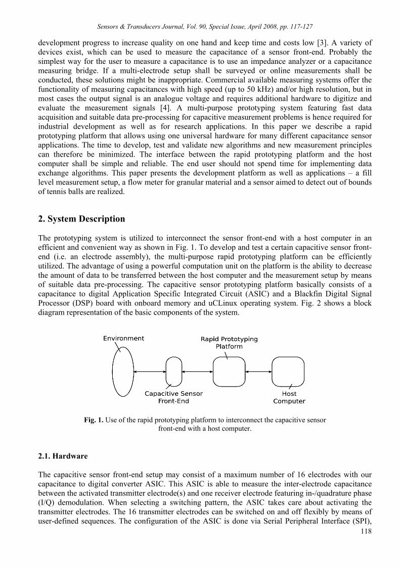
Sensors & Transducers Journal, Vol. 90, Special Issue, April 2008, pp. 117-127
118
development progress to increase quality on one hand and keep time and costs low [3]. A variety of devices exist, which can be used to measure the capacitance of a sensor front-end. Probably the simplest way for the user to measure a capacitance is to use an impedance analyzer or a capacitance measuring bridge. If a multi-electrode setup shall be surveyed or online measurements shall be conducted, these solutions might be inappropriate. Commercial available measuring systems offer the functionality of measuring capacitances with high speed (up to 50 kHz) and/or high resolution, but in most cases the output signal is an analogue voltage and requires additional hardware to digitize and evaluate the measurement signals [4]. A multi-purpose prototyping system featuring fast data acquisition and suitable data pre-processing for capacitive measurement problems is hence required for industrial development as well as for research applications. In this paper we describe a rapid prototyping platform that allows using one universal hardware for many different capacitance sensor applications. The time to develop, test and validate new algorithms and new measurement principles can therefore be minimized. The interface between the rapid prototyping platform and the host computer shall be simple and reliable. The end user should not spend time for implementing data exchange algorithms. This paper presents the development platform as well as applications – a fill level measurement setup, a flow meter for granular material and a sensor aimed to detect out of bounds of tennis balls are realized. 2. System Description The prototyping system is utilized to interconnect the sensor front-end with a host computer in an efficient and convenient way as shown in Fig. 1. To develop and test a certain capacitive sensor front-end (i.e. an electrode assembly), the multi-purpose rapid prototyping platform can be efficiently utilized. The advantage of using a powerful computation unit on the platform is the ability to decrease the amount of data to be transferred between the host computer and the measurement setup by means of suitable data pre-processing. The capacitive sensor prototyping platform basically consists of a capacitance to digital Application Specific Integrated Circuit (ASIC) and a Blackfin Digital Signal Processor (DSP) board with onboard memory and uCLinux operating system. Fig. 2 shows a block diagram representation of the basic components of the system.
Fig. 1. Use of the rapid prototyping platform to interconnect the capacitive sensor front-end with a host computer.
2.1. Hardware The capacitive sensor front-end setup may consist of a maximum number of 16 electrodes with our capacitance to digital converter ASIC. This ASIC is able to measure the inter-electrode capacitance between the activated transmitter electrode(s) and one receiver electrode featuring in-/quadrature phase (I/Q) demodulation. When selecting a switching pattern, the ASIC takes care about activating the transmitter electrodes. The 16 transmitter electrodes can be switched on and off flexibly by means of user-defined sequences. The configuration of the ASIC is done via Serial Peripheral Interface (SPI),

Sensors & Transducers Journal, Vol. 90, Special Issue, April 2008, pp. 117-127
119
while the high speed data transfer of the measurement results is done via parallel bus. A Blackfin uCLinux stamp board is used as interface, data processing, and communication platform. This board is equipped with an Analog Devices Blackfin DSP, 64 MB of SDRAM and 4 MB of Flash memory to store the bootloader and the uCLinux kernel image. The Blackfin DSP is well suited for a rapid prototyping platform due to its exceptional wide range of peripheral interfaces. The Blackfin BF537 DSP offers synchronous and asynchronous serial ports, high speed parallel interfaces, GPIOs and even 10/100 MBit Ethernet. The maximum core clock frequency reaches 600 MHz with a system bus frequency of up to 100 MHz. As one of the fastest representatives of the Blackfin series, the BF537 reaches a computation power of up to 1200 Million Multiply Accumulate (MMAC) operations per second. A photo of the rapid prototyping platform is shown in Fig. 3.
Fig. 2. Block diagram of the basic components of the rapid prototyping platform and the capacitive sensor setup
(front-end).
Fig. 3. Photo of the rapid prototyping platform comprising Blackfin Stamp board and ASIC board. 2.2. Software One aim of the prototyping platform is that the user should not spend much time for implementing data exchange interfaces. An uCLinux operating system is hence used, which allows for a convenient, fast

Sensors & Transducers Journal, Vol. 90, Special Issue, April 2008, pp. 117-127
120
and reliable data transfer. In contrast to a conventional Linux operating system uCLinux has the ability to run on processors without a Memory Management Unit (MMU–less systems). Access to peripherals is gained by kernel modules. In the current version of the prototyping platform, one kernel module for the DSP parallel port is used and another one for the SPI port. Data transfer from parallel interface into the DSP memory is done by Direct Memory Access (DMA). This allows for the CPU to compute output data, e.g. correlation or frequency estimation routines, while receiving new measurement values. Another advantage of grabbing parallel data via DMA is the real-time capability of the overall system due to the external clock driven DMA transfer, although the uCLinux system itself cannot guarantee real-time behavior. 2.3. Host Communication One of the most comfortable solutions for transferring data is an interface via uCLinux built-in web server. The programmed measurement routine on the DSP may write data into a specific folder, which is accessible by any web browser. This allows complete stand-alone sensor solutions. If higher data transfer rates are required, a socket communication is implemented, where a measurement daemon listens on a predefined “socket” for incoming commands. In case of a measurement command, the daemon starts the measurement and appropriate signal processing routines and sends the desired information back to the host system through the socket. On the host side both communication approaches can be easily implemented in MATLAB, LabView, C or any other programming language. Furthermore, data interpretation algorithms developed in C on the host side may be cross-compiled for Blackfin uCLinux without any changes and can be executed directly on the DSP to eliminate data transmission latency and provide a stand-alone sensor solution. 2.4. System Performance The capacitance to digital converter ASIC is capable of handling electrode layouts with an offset capacity of up to 20 pF, while the measurable capacitance variations are in the range of some fF. A large number of capacitive sensor applications with a wide variety of different demands can hence be served. Commercially available circuitries [4], [5] typically offer high resolutions at low measurement rates. Our capacitance measurement system provides a lower resolution of 10 bit but can be operated at high measurement rates. The current setup allows for measurement rates of up to approximately 100 kHz for a single electrode and approximately 6 kHz for complete measurement cycles of 16 electrodes respectively. The number of active transmitter electrodes, as well as their measurement frequency can be easily set by software. Furthermore, analog gain and offset can be tuned by software to adopt the rapid prototyping platform to electrode structures of various dimensions. 3. Applications for the Prototyping Platform To show the practical benefit of the rapid prototyping platform, three exemplary applications are implemented and have been tested. In all cases, the platform is just plugged to the electrode structure of the sensor front-end. The first example is a capacitive fill level sensor, which is designed for non-invasive fill level monitoring of fuel or water vessels. In a second example we show a possible setup for capacitive velocimetry of moving particles in a pipe, which is a frequent measurement task in pneumatic conveying of bulk solids. A third setup shows the applicability of the rapid prototyping platform for the detection of hits of a tennis ball aimed to be used in sports to support referees in their in/out bound decision.

Sensors & Transducers Journal, Vol. 90, Special Issue, April 2008, pp. 117-127
121
3.1. Fill Level Measurements Fill level determination by means of capacitive sensing is a frequently arising measurement problem in process instrumentation [6], [7], [8]. For the measurement setup in our application, a non-conducting cylindrical vessel was equipped with a pump and an outlet valve to control the water fill level in the vessel. A calliper is used to provide reference data of the fill level height. One receiver electrode and 16 transmitter electrodes are mounted in parallel along the vertical axis on the vessels outside (see Fig. 4). The liquid inside the vessel causes a change in dielectric permittivity for the region around the transmitter electrodes (i.e. in the sensitive region of the individual electrode) below the fill level. The capacitance between each active transmitter segment and the receiver is increased in case of presence of water (εr = 80) in the vicinity of the segment. This sensor principle can be applied to a wide variety of fill level measurement problems. A sensor element comprising 16 transmitter and one receiver electrode can be mounted inside a tank, if the tank is made of conductive material and the liquid is non-aggressive. Or, if a non-conductive material is used, like for automotive tanks, the sensor can be mounted on the outer surface of the tank. The sensor resolution can be increased by an arbitrary application specific design of the electrode geometry. Transmitter electrodes are operated in time division multiple access (i.e. all transmitters are activated one after the other and there is always just one transmitter active at a time). Our approach to determine the fill level is to accumulate all single capacitance values and to normalize them as shown in Fig. 5. The measurement results show that the curve is not straightly linear. This effect is most likely caused by the imperfect printed electrode layout, in particular due to transmitter and receiver wire routing. The nonlinearity could be handled either by a carefully designed electrode layout or by a calibration of the sensor setup. Note that the entire fill level computation can be done onboard on the rapid prototyping platform and that the actual fill level can be directly provided either in digital form for example by means of Controller Area Network (CAN) or as an analogous signal like a 4-20 mA current output.
Fig. 4. Schematic electrode layout for measuring liquid fill level with 16 transmitter and one receiver electrode.
3.2. Velocity Determination by Means of Spatial Filtering The basis of spatial filtering methods [9], [10] is the evaluation of signal amplitudes caused by moving particles through grating-like structures. Bypassing particles have an impact on the readout of the measurement signal, which is dependent on the particle velocity and on the geometrical dimensions of the sensing volume. For a given sequence of sensitive volumes with a certain extend in flow direction, a slow particle will cause lower frequency contributions than a fast moving particle will. The basic principle of velocity determination by means of spatial filtering is shown in Fig. 6. In our setup, eight pairs of electrodes are mounted on the outer surface of a non conducting pipe with a diameter of
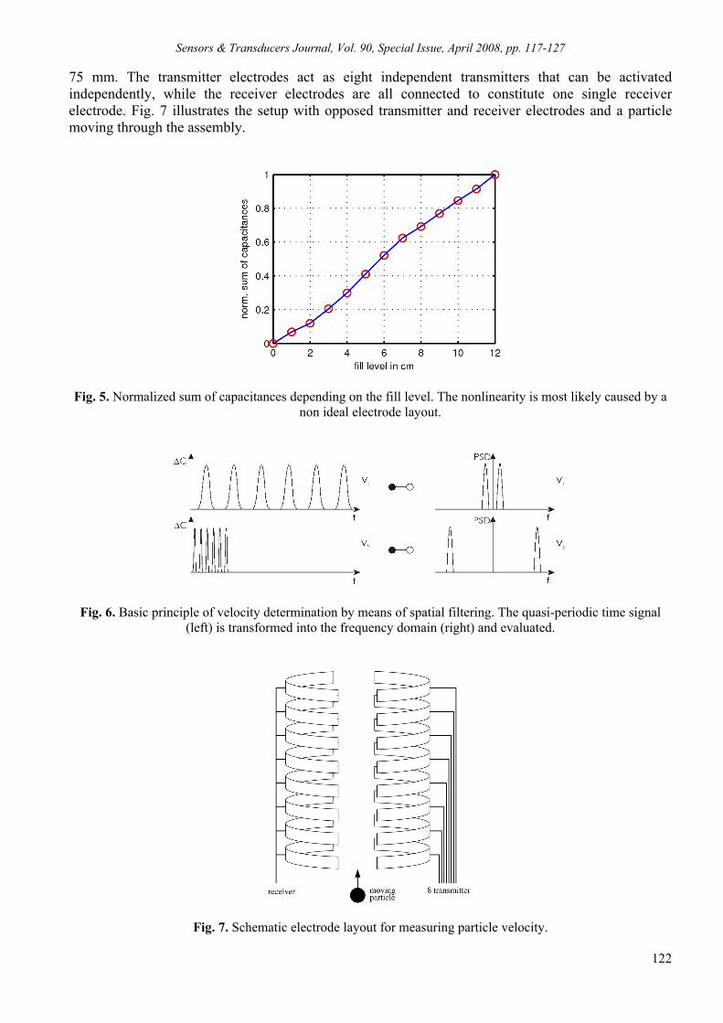
Sensors & Transducers Journal, Vol. 90, Special Issue, April 2008, pp. 117-127
122
75 mm. The transmitter electrodes act as eight independent transmitters that can be activated independently, while the receiver electrodes are all connected to constitute one single receiver electrode. Fig. 7 illustrates the setup with opposed transmitter and receiver electrodes and a particle moving through the assembly.
Fig. 5. Normalized sum of capacitances depending on the fill level. The nonlinearity is most likely caused by a non ideal electrode layout.
Fig. 6. Basic principle of velocity determination by means of spatial filtering. The quasi-periodic time signal (left) is transformed into the frequency domain (right) and evaluated.
Fig. 7. Schematic electrode layout for measuring particle velocity.

Sensors & Transducers Journal, Vol. 90, Special Issue, April 2008, pp. 117-127
123
An electrode structure like the one presented in Fig. 7 does not feature constant sensitivity over the whole pipe cross-section. There are areas of higher sensitivity (close to the gap between transmitter and receiver electrodes) and lower sensitivity (e.g. at the pipe center or close to the electrode centers). To test the setup and to allow for reproducible measurement results, a motor-driven setup is used to move a wooden sphere with a diameter of 23 mm on a thin nylon line through the electrode array. The velocity of the moving sphere can be varied by changing the motor rotation speed. Measurement results acquired with the rapid prototyping system are shown in Fig. 8. In this experiment, the sphere was moved through the sensitive volume with lower velocity first and then with approximately double speed. To evaluate the functionality of the capacitive flow sensor principle for granular material flow, the sensor was tested at a laboratory conveying rig. In this setup monodisperse plastic pellets are conveyed using airflow in a closed pipe produced by a fan. A throttle flap allows for the adjustment of the conveyed air mass and hence of the number of conveyed particles. The transmitter and receiver electrodes are mounted on the outer surface of a pipe with a diameter of 75 mm. Fig. 9 shows, that the sensor setup is able to track even single particles with a size of 4 mm and a permittivity εr of about 3. The sequence of 0.2 s is recorded with a sample rate of 16 kHz. At time steps 0.12 s and at 0.22 s two passing particles cause four periods in the output signal of the spatial filter.
Fig. 8. Measured capacitance variation over time. The particle velocity in the first burst is approximately two times lower than in the second burst.
To estimate the particle velocity frequency estimation, based on a Fourier Frequency Analysis, is applied. Fig. 10 shows the estimated frequency for three different throttle flap positions. The lower spectral power for slow particles results from a lower number of conveyed particles within the measurement time window and therefore an inferior measurement signal energy. For the measured results in Fig. 9 and 10 a differential excitation of electrodes has been used, i.e. transmitter electrodes are subsequently excited with alternating polarity [11].
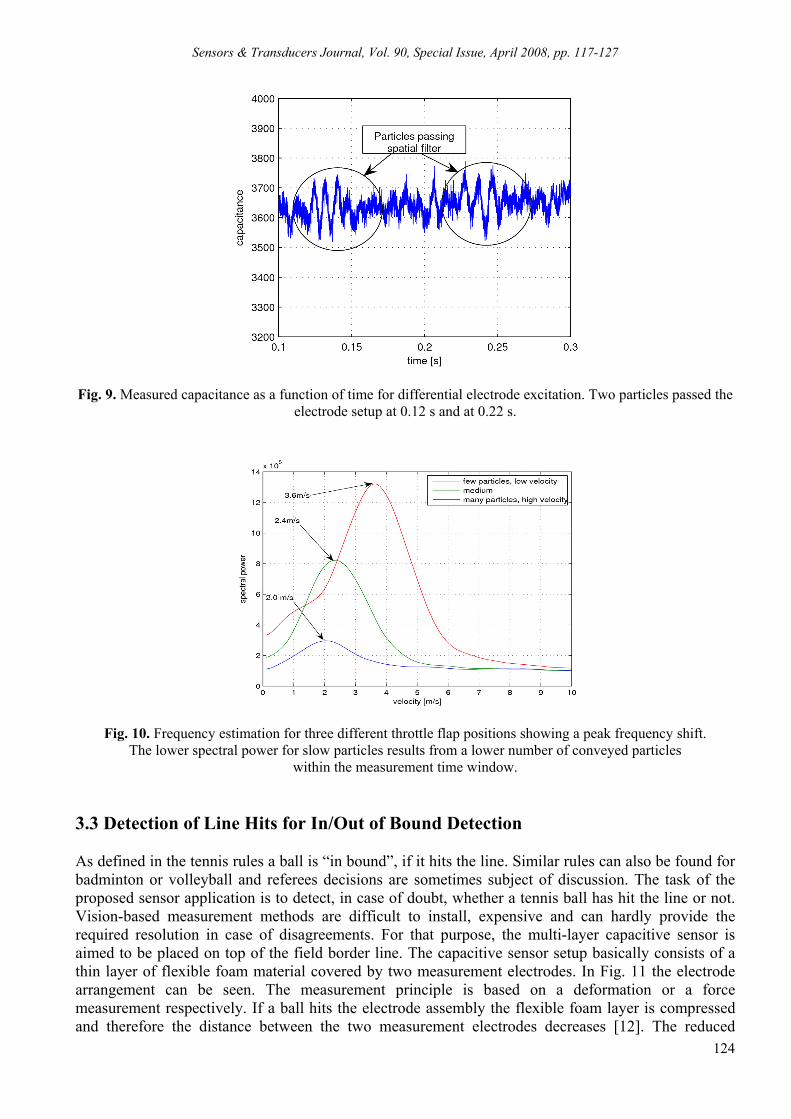
Sensors & Transducers Journal, Vol. 90, Special Issue, April 2008, pp. 117-127
124
Fig. 9. Measured capacitance as a function of time for differential electrode excitation. Two particles passed the
electrode setup at 0.12 s and at 0.22 s.
Fig. 10. Frequency estimation for three different throttle flap positions showing a peak frequency shift. The lower spectral power for slow particles results from a lower number of conveyed particles
within the measurement time window. 3.3 Detection of Line Hits for In/Out of Bound Detection As defined in the tennis rules a ball is “in bound”, if it hits the line. Similar rules can also be found for badminton or volleyball and referees decisions are sometimes subject of discussion. The task of the proposed sensor application is to detect, in case of doubt, whether a tennis ball has hit the line or not. Vision-based measurement methods are difficult to install, expensive and can hardly provide the required resolution in case of disagreements. For that purpose, the multi-layer capacitive sensor is aimed to be placed on top of the field border line. The capacitive sensor setup basically consists of a thin layer of flexible foam material covered by two measurement electrodes. In Fig. 11 the electrode arrangement can be seen. The measurement principle is based on a deformation or a force measurement respectively. If a ball hits the electrode assembly the flexible foam layer is compressed and therefore the distance between the two measurement electrodes decreases [12]. The reduced
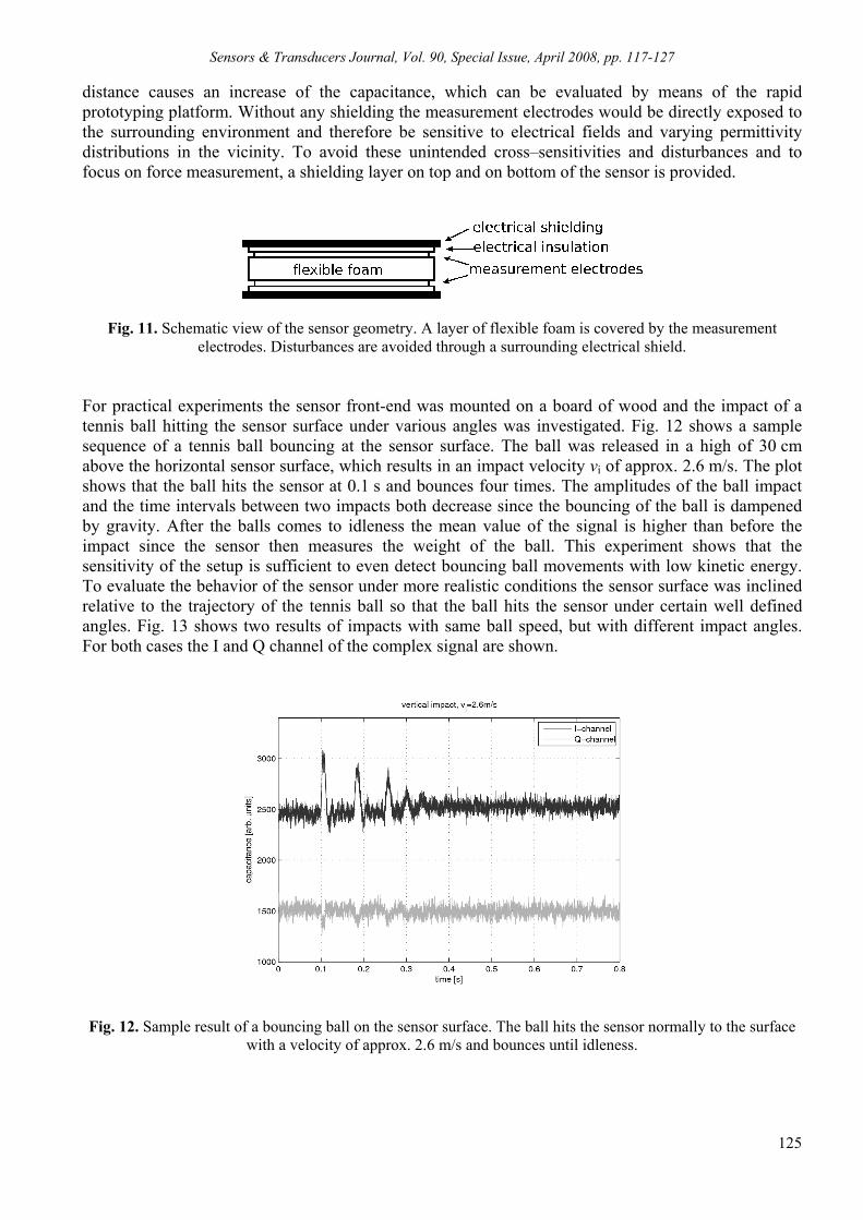
Sensors & Transducers Journal, Vol. 90, Special Issue, April 2008, pp. 117-127
125
distance causes an increase of the capacitance, which can be evaluated by means of the rapid prototyping platform. Without any shielding the measurement electrodes would be directly exposed to the surrounding environment and therefore be sensitive to electrical fields and varying permittivity distributions in the vicinity. To avoid these unintended cross–sensitivities and disturbances and to focus on force measurement, a shielding layer on top and on bottom of the sensor is provided.
Fig. 11. Schematic view of the sensor geometry. A layer of flexible foam is covered by the measurement electrodes. Disturbances are avoided through a surrounding electrical shield.
For practical experiments the sensor front-end was mounted on a board of wood and the impact of a tennis ball hitting the sensor surface under various angles was investigated. Fig. 12 shows a sample sequence of a tennis ball bouncing at the sensor surface. The ball was released in a high of 30 cm above the horizontal sensor surface, which results in an impact velocity vi of approx. 2.6 m/s. The plot shows that the ball hits the sensor at 0.1 s and bounces four times. The amplitudes of the ball impact and the time intervals between two impacts both decrease since the bouncing of the ball is dampened by gravity. After the balls comes to idleness the mean value of the signal is higher than before the impact since the sensor then measures the weight of the ball. This experiment shows that the sensitivity of the setup is sufficient to even detect bouncing ball movements with low kinetic energy. To evaluate the behavior of the sensor under more realistic conditions the sensor surface was inclined relative to the trajectory of the tennis ball so that the ball hits the sensor under certain well defined angles. Fig. 13 shows two results of impacts with same ball speed, but with different impact angles. For both cases the I and Q channel of the complex signal are shown.
Fig. 12. Sample result of a bouncing ball on the sensor surface. The ball hits the sensor normally to the surface
with a velocity of approx. 2.6 m/s and bounces until idleness.

Sensors & Transducers Journal, Vol. 90, Special Issue, April 2008, pp. 117-127
126
Fig. 13. Sample results of a ball hitting the surface under an angle of 45 degrees (left, time step 0.17 s) and 25 degrees (right, time step 1.08 s). The impact velocity is 4.6 m/s in both cases.
4 Conclusions In this paper we present a versatile rapid prototyping platform for a wide range of capacitive applications to be found in modern sensing. The platform allows developers to reduce the design- and evaluation time for new capacitive measurement principles and new electrode topologies. It provides high data acquisition rates and a high computational power allowing for the implementation of sophisticated signal processing algorithms in stand-alone applications. The hardware is based on an Analog Devices Blackfin DSP in conjunction with a capacitance to digital converter ASIC. The DSP runs on an uCLinux operating system and therefore offers easy access to measurement data by 10/100 Mbit TCP/IP network interface, CAN bus or analogous outputs. Functionality and applicability for various capacitive sensor architectures is shown in three different sensor realizations, namely a liquid fill level-, a flow sensor, and tennis in/out of border detection. The experiments show, that although the number and dimensions of the electrodes differ in the three applications, the multi-purpose platform can be utilized without requiring any hardware adjustments. Acknowledgments This work was partially funded by the Austrian Science Fund through the Translational Research Project number L355-N20 and the Christian Doppler Laboratory for Automotive Measurement Research. References [1]. G. Brasseur, Design Rules for Robust Capacitive Sensors, IEEE Transactions on Instrumentation and
Measurement, Vol. 52, No. 4, 2003, pp. 1261-1265. [2]. L. K. Baxter, Capacitive Sensors - Design and Application, IEEE Press Series on Electronics Technology,
New York, 1997. [3]. B. Spitzer, A. Burst, M. Wolff, K. Muller- Glaser, Interface Technologies for Versatile Rapid Prototyping
Systems, Proceedings of the IEEE International Workshop on Rapid System Prototyping, 16-18 June 1999, 1999, pp. 204-209.
[4]. Kompaktsystem capaNCDT 6100, Micro-Epsilon datasheet, available on www.micro-epsilon.de, visited

Sensors & Transducers Journal, Vol. 90, Special Issue, April 2008, pp. 117-127
127
12.07.2007. [5]. AD7745 24-bit, 1 Channel Capacitance to Digital Converter, Analog Devices datasheet, available on
www.analog.com, visited 17.09.2007. [6]. F. Reverter, M. Gasulla, R. Pallas-Areny, Capacitive Level Sensing for Solid-Waste Collection,
Proceedings of the IEEE Sensor 2003, 22-24. October 2003, Vol. 1, 2003, pp. 7-11. [7]. F. N. Toth, G. C. Meijer, M. van der Lee, A planar capacitive precision gauge for liquid-level and leakage
detection, IEEE Transactions on Instrumentation and Measurement, Vol. 46, No. 2, 1997, pp. 644-646. [8]. T. Mohr, U. Ehrenberg, H. Uhlmann, A new Method for a self-calibrating capacitive sensor, Proceedings
of the 18th IEEE Instrumentation and Measurement Technology Conference, IMTC, 21- 23 May 2001, Vol. 1, 2001, pp. 454-459.
[9]. E.A. Hammer, and R.G. Green, The spatial filtering effect of capacitance transducer electrodes, Journal of Physics E: Scientific Instruments, Vol. 16, 1983, pp. 438-443.
[10]. Y. Yan, Mass flow measurement of bulk solids in pneumatic pipelines, Measurement Science and Technology, Vol. 7, 1996, pp. 1687-1706.
[11]. D. Hrach, A. Fuchs, and H. Zangl, Capacitive Flowmeter for Gas-Solids Flow Applications Exploiting Spatial Frequency, To be published in the Proceedings of the Sensor Applications Symposium 2008, SAS2008 Atlanta, 2008.
[12]. J. Yuji, and C. Sonoda, A Capacitive PVDF Tactile Sensor with Contact Force and Temperature Sensing Function, Proceedings of the 2nd International Conference on Sensing Technology, ICST2007, 26-28 Nov., 2007, pp. 68-73.
[13]. D. Hrach, A. Fuchs, H. Zangl, and T. Bretterklieber, A Rapid Prototyping Platform for Capacitive Measurement Systems, Proceedings of the 2nd International Conference on Sensing Technology, ICST, 26-28 November 2007, 2008, pp. 441-446.
___________________
2008 Copyright ©, International Frequency Sensor Association (IFSA). All rights reserved. (http://www.sensorsportal.com)
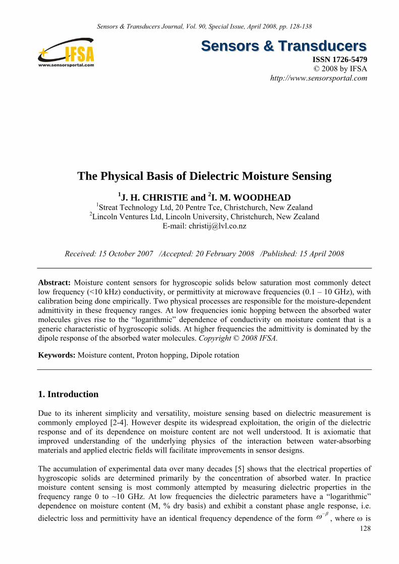
Sensors & Transducers Journal, Vol. 90, Special Issue, April 2008, pp. 128-138
128
SSSeeennnsssooorrrsss &&& TTTrrraaannnsssddduuuccceeerrrsss
ISSN 1726-5479© 2008 by IFSA
http://www.sensorsportal.com
The Physical Basis of Dielectric Moisture Sensing
1J. H. CHRISTIE and 2I. M. WOODHEAD
1Streat Technology Ltd, 20 Pentre Tce, Christchurch, New Zealand 2Lincoln Ventures Ltd, Lincoln University, Christchurch, New Zealand
E-mail: [email protected]
Received: 15 October 2007 /Accepted: 20 February 2008 /Published: 15 April 2008 Abstract: Moisture content sensors for hygroscopic solids below saturation most commonly detect low frequency (<10 kHz) conductivity, or permittivity at microwave frequencies (0.1 – 10 GHz), with calibration being done empirically. Two physical processes are responsible for the moisture-dependent admittivity in these frequency ranges. At low frequencies ionic hopping between the absorbed water molecules gives rise to the “logarithmic” dependence of conductivity on moisture content that is a generic characteristic of hygroscopic solids. At higher frequencies the admittivity is dominated by the dipole response of the absorbed water molecules. Copyright © 2008 IFSA. Keywords: Moisture content, Proton hopping, Dipole rotation 1. Introduction Due to its inherent simplicity and versatility, moisture sensing based on dielectric measurement is commonly employed [2-4]. However despite its widespread exploitation, the origin of the dielectric response and of its dependence on moisture content are not well understood. It is axiomatic that improved understanding of the underlying physics of the interaction between water-absorbing materials and applied electric fields will facilitate improvements in sensor designs. The accumulation of experimental data over many decades [5] shows that the electrical properties of hygroscopic solids are determined primarily by the concentration of absorbed water. In practice moisture content sensing is most commonly attempted by measuring dielectric properties in the frequency range 0 to ~10 GHz. At low frequencies the dielectric parameters have a “logarithmic” dependence on moisture content (M, % dry basis) and exhibit a constant phase angle response, i.e. dielectric loss and permittivity have an identical frequency dependence of the form
βω−, where ω is

Sensors & Transducers Journal, Vol. 90, Special Issue, April 2008, pp. 128-138
129
the radial frequency and β is a constant. The magnitude of the specific admittance (admittivity) decreases linearly in logarithmic representation to a change of slope at intermediate frequencies (~10-1 – 105 Hz). The characteristics of the intermediate frequency response vary between different materials and the nature of the underlying process is unclear. At higher frequencies classical dipole dispersion is observed with a relaxation frequency ~109 Hz and magnitude linearly dependent on M. Two variables commonly determine the minimum signal frequency that can be used: the first is the time constant of the process to be controlled, which in the case of industrial drying for example can be on the order of minutes, allowing frequencies as low as 0.01 Hz to be used. The second and usually controlling variable is the maximum rate of change of moisture content in the target material. Since the relationship between low frequency dielectric data and moisture content is non-linear, the minimum measurement frequency should be between 1 and 2 orders of magnitude higher than the maximum frequency of moisture content variation. However experimental measurement of dielectric properties should be made over as wide range as possible as an aid to correct interpretation of the data; this is the approach that has been taken here. In the following sections we present experimental data illustrating the generic characteristics of hygroscopic solids, and then develop an electrical model for the entire frequency range over which the presence of absorbed water can significantly affect their properties. 2. Experimental The 600 Hz relative conductance of commercial samples of rubber coir, chocolate crumb and gelatine were measured at room temperature using the Streat Instruments Ltd Drycom Moisture Meter. Measurements on a single sheet of chemically cleaned cellophane were performed in a vacuum chamber in which water vapour pressure could be varied and temperature controlled to ±0.1°C. The sample was mounted in a guarded cell with aluminium foil electrodes. A second sample mounted on a Mettler Toledo SAG204 weighing balance in the chamber served to verify stability and to determine M. The dry weight was obtained by placing anhydrous P2O5 in the chamber. The voltage source was an Agilent 33120A Function Generator. Voltage and current were detected with a purpose-built amplifier. Frequencies from 1 x 10⁻³ to 3 x 101 Hz were measured digitally, while from 3 x 100 to 3 x 10⁵ Hz amplitude was measured with an HP 34401A multimeter and phase angle with an analogue circuit. 3. Results and Discussion 3.1. Low Frequency Region - Moisture Content Dependence Fig. 1 shows typical conductance versus moisture content data measured with the Drycom moisture meter. Similar data were observed for many other industrial products, including for example bread crumbs, olive pomace, wool, cotton, viscose, nylon and possum fur. Fig. 2 shows typical data taken from the literature. The implication of these data and of many others that can be found in the literature is that “logarithmic” dependence of low frequency conductivity on M is a universal characteristic of hygroscopic solids.

Sensors & Transducers Journal, Vol. 90, Special Issue, April 2008, pp. 128-138
130
0.0
2.0
4.0
6.0
0 10 20 30
Moisture content, %
Log
cond
ucta
nce,
a.u
.Chocolate crumbGelatineRubber coir
Fig. 1. The room temperature conductance of rubber coir, gelatine and chocolate crumb at 600 Hz, a.u. = arbitrary units. The latter two data sets have been offset by +1 for clarity.
-15.0
-13.0
-11.0
-9.0
0 5 10
Moisture content, %
Log
cond
uctiv
ity, S
/m
Fig. 2. The low frequency conductivity of nylon at 25°C [6]. Similar data were obtained by Hearle [7] for a large number of textile fibres.
As a step towards theoretical interpretation many investigators have attempted to identify the charge carrier [8-15]. Whereas the evidence in favour of electrons is weak, conduction by impurity ions has been demonstrated directly [16-18] and the evidence for protonic conduction is strong [14, 15, 19, 20]. Fig. 3 shows the conductivity of two samples of deuterated lysozyme measured in a high (>106 V/m) electric field [18]. One sample contained mobile impurity ions and in the other these ions had been removed electrically (“Uncleaned” and “Cleaned” respectively). Conductivity was calculated from the electrical measurements and from the quantities of deuterium gas collected (“Deuterium”), the latter being found to be independent of the impurity ion concentration.
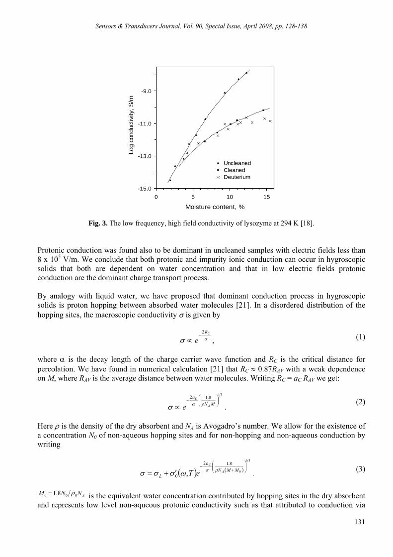
Sensors & Transducers Journal, Vol. 90, Special Issue, April 2008, pp. 128-138
131
-15.0
-13.0
-11.0
-9.0
0 5 10 15
Moisture content, %
Log
cond
uctiv
ity, S
/m
UncleanedCleanedDeuterium
Fig. 3. The low frequency, high field conductivity of lysozyme at 294 K [18]. Protonic conduction was found also to be dominant in uncleaned samples with electric fields less than 8 x 10⁵ V/m. We conclude that both protonic and impurity ionic conduction can occur in hygroscopic solids that both are dependent on water concentration and that in low electric fields protonic conduction are the dominant charge transport process. By analogy with liquid water, we have proposed that dominant conduction process in hygroscopic solids is proton hopping between absorbed water molecules [21]. In a disordered distribution of the hopping sites, the macroscopic conductivity σ is given by
ασCR
e2
−∝ , (1)
where α is the decay length of the charge carrier wave function and RC is the critical distance for percolation. We have found in numerical calculation [21] that RC ≈ 0.87RAV with a weak dependence on M, where RAV is the average distance between water molecules. Writing RC = aC RAV we get: 31
8.12⎟⎟⎠
⎞⎜⎜⎝
⎛−
∝ MNa
A
C
e ρασ . (2)
Here ρ is the density of the dry absorbent and NA is Avogadro’s number. We allow for the existence of a concentration N0 of non-aqueous hopping sites and for non-hopping and non-aqueous conduction by writing
( ) ( )
31
0
8.12
0 ,⎟⎟⎠
⎞⎜⎜⎝
⎛+
−
′+= MMNa
LA
C
eT ραωσσσ . (3)
ANNM 000 8.1 ρ= is the equivalent water concentration contributed by hopping sites in the dry absorbent
and represents low level non-aqueous protonic conductivity such as that attributed to conduction via
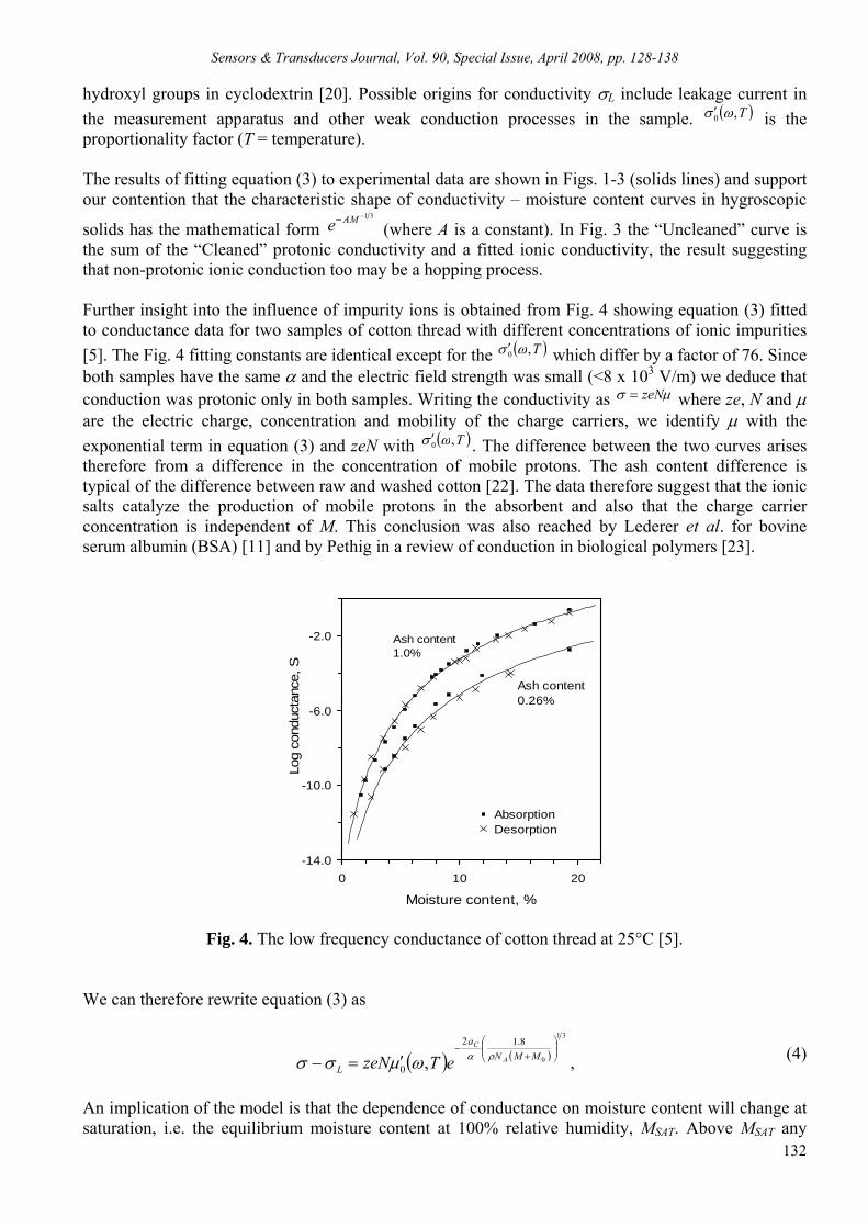
Sensors & Transducers Journal, Vol. 90, Special Issue, April 2008, pp. 128-138
132
hydroxyl groups in cyclodextrin [20]. Possible origins for conductivity σL include leakage current in the measurement apparatus and other weak conduction processes in the sample. ( )T,0 ωσ ′ is the proportionality factor (T = temperature). The results of fitting equation (3) to experimental data are shown in Figs. 1-3 (solids lines) and support our contention that the characteristic shape of conductivity – moisture content curves in hygroscopic
solids has the mathematical form 31−−AMe (where A is a constant). In Fig. 3 the “Uncleaned” curve is
the sum of the “Cleaned” protonic conductivity and a fitted ionic conductivity, the result suggesting that non-protonic ionic conduction too may be a hopping process. Further insight into the influence of impurity ions is obtained from Fig. 4 showing equation (3) fitted to conductance data for two samples of cotton thread with different concentrations of ionic impurities [5]. The Fig. 4 fitting constants are identical except for the ( )T,0 ωσ ′ which differ by a factor of 76. Since both samples have the same α and the electric field strength was small (<8 x 10³ V/m) we deduce that conduction was protonic only in both samples. Writing the conductivity as µσ zeN= where ze, N and µ are the electric charge, concentration and mobility of the charge carriers, we identify µ with the exponential term in equation (3) and zeN with ( )T,0 ωσ ′ . The difference between the two curves arises therefore from a difference in the concentration of mobile protons. The ash content difference is typical of the difference between raw and washed cotton [22]. The data therefore suggest that the ionic salts catalyze the production of mobile protons in the absorbent and also that the charge carrier concentration is independent of M. This conclusion was also reached by Lederer et al. for bovine serum albumin (BSA) [11] and by Pethig in a review of conduction in biological polymers [23].
-14.0
-10.0
-6.0
-2.0
0 10 20
Moisture content, %
Log
cond
ucta
nce,
S
Ash content 1.0%
Ash content 0.26%
AbsorptionDesorption
Fig. 4. The low frequency conductance of cotton thread at 25°C [5].
We can therefore rewrite equation (3) as
( ) ( )
31
0
8.12
0 ,⎟⎟⎠
⎞⎜⎜⎝
⎛+
−
′=− MMNa
LA
C
eTzeN ραωµσσ , (4)
An implication of the model is that the dependence of conductance on moisture content will change at saturation, i.e. the equilibrium moisture content at 100% relative humidity, MSAT. Above MSAT any

Sensors & Transducers Journal, Vol. 90, Special Issue, April 2008, pp. 128-138
133
further increases in M occur by condensation on external surfaces. RC therefore remains constant, and the shape of the theoretical curve will change. Fig. 5 shows equation (3) fitted to data for viscose (33% ≤ MSAT ≤ 45% [24]). A change from a “logarithmic” to approximately linear characteristic occurs at M ≈ 35%.
Fig. 5. The low frequency conductance of viscose at 20°C [7] plotted in log and linear representation. 3.2. Low Frequency Region - Frequency Dependence Figs. 6 and 7 show the dielectric spectra of cellophane from 10-3 – 105 Hz for three different M.
-10.0
-8.0
-6.0
-4.0
-2.0
0.0
-3 -1 1 3 5
Log frequency, Hz
Log
cond
uctiv
ity, S
/m
33.4%
15.0%
9.0%
Fig. 6. The conductivity of cellophane at 30.9°C for M = 9.0%, 15.0% and 33.4%.
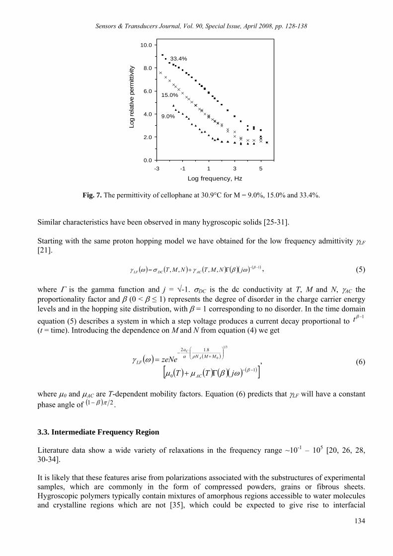
Sensors & Transducers Journal, Vol. 90, Special Issue, April 2008, pp. 128-138
134
0.0
2.0
4.0
6.0
8.0
10.0
-3 -1 1 3 5
Log frequency, Hz
Log
rela
tive
perm
ittiv
ity
33.4%
15.0%
9.0%
Fig. 7. The permittivity of cellophane at 30.9°C for M = 9.0%, 15.0% and 33.4%. Similar characteristics have been observed in many hygroscopic solids [25-31]. Starting with the same proton hopping model we have obtained for the low frequency admittivity γLF [21]. ( ) ( ) ( ) ( )( ) ( )1,,,, −−Γ+= βωβγσωγ jNMTNMT ACDCLF
, (5) where Γ is the gamma function and j = √-1. σDC is the dc conductivity at T, M and N, γAC the proportionality factor and β (0 < β ≤ 1) represents the degree of disorder in the charge carrier energy levels and in the hopping site distribution, with β = 1 corresponding to no disorder. In the time domain equation (5) describes a system in which a step voltage produces a current decay proportional to
1−βt (t = time). Introducing the dependence on M and N from equation (4) we get
( ) ( )
( ) ( ) ( )( ) ( )[ ]10
8.1231
0
−−
⎟⎟⎠
⎞⎜⎜⎝
⎛+
−
Γ+
=β
ρα
ωβµµ
ωγ
jTT
zeNe
AC
MMNa
LFA
C
, (6)
where µ0 and µAC are T-dependent mobility factors. Equation (6) predicts that γLF will have a constant phase angle of ( ) 21 πβ− . 3.3. Intermediate Frequency Region Literature data show a wide variety of relaxations in the frequency range ~10-1 – 105 [20, 26, 28, 30-34]. It is likely that these features arise from polarizations associated with the substructures of experimental samples, which are commonly in the form of compressed powders, grains or fibrous sheets. Hygroscopic polymers typically contain mixtures of amorphous regions accessible to water molecules and crystalline regions which are not [35], which could be expected to give rise to interfacial

Sensors & Transducers Journal, Vol. 90, Special Issue, April 2008, pp. 128-138
135
polarisations. We interpret the change of slope at the high frequency end of the cellophane data as arising from this cause. The charge carrier transit time in sub-structure units is inversely proportional to the mobility which for constant N is proportional to the admittivity. From equation (5) and anticipating σDC ≈ 0, β ≈ 1, we see that the transit time is approximately proportional to 1/γAC(M) so relaxation frequency ω0 α γAC(M). The loss peak amplitude is proportional to ( ) ( )
01
0 ωωγ β−−MAC (equation (5)) which is a constant. Such behaviour has been observed experimentally in BSA [33] and lysozyme [34], supporting our interpretation of intermediate frequency relaxations. A similar conclusion has been reached regarding intermediate frequency dispersion in ovalbumin [36]. To represent the contribution of the intermediate frequency relaxation to total admittance we add a general function γIF which could represent, for example, the Havriliak-Negami function [37] which was found to fit data for BSA [33] or the Davidson-Cole model which fitted ovalbumin data [36]. 3.4. High Frequency Region A classical Debye dipolar dispersion detected in lysozyme at 0.2 GHz and M = 34% by Harvey et al. [38], and a similar response has been obtained in BSA, with magnitude proportional to the amount of primary absorbed water [39]. A dipolar response at frequencies below that for bulk water would be expected in view of the stronger bonding experienced by absorbed water. We represent the high frequency response with a Debye function, since this was found to accurately fit experimental data for lysozyme [38]:
⎟⎟⎠
⎞⎜⎜⎝
⎛+
+= ∞D
DHF j
Mjωτε
ρεωγ1
100 , (7)
Here Dε is the magnitude of the dipole relaxation per kg of absorbed water, τD is its relaxation time, ρ is the density of the dry absorbent and
∞ε is the high frequency limiting value of the permittivity. 3.5. Application of the Model to Cellophane The equation
HFIFLF γγγγ ++= , (8) has been fitted to the cellophane data shown in Figs. 6 and 7. The data for the intermediate frequency response is too limited for any meaningful analysis so simple functions of the form ( ))1−− nω were used for the real and imaginary parts of γIF. We used 0εε∞ = 3, 0100€ εερ D = 15/34 (values for lysozyme [38] assumed, ε0 = the permittivity of free space) and ωτD = 0 for γHF. The dc conductivity was treated as a fitting parameter. The results are shown in Fig. 8 for M = 9.0% and 33.4%, and in Table 1. Since the gradients for both the ε′ and ε″ lines at low frequencies and the magnitude difference (in logarithmic representation) are all determined by a single value of β, the fits obtained give good support to the model represented by equation (6).

Sensors & Transducers Journal, Vol. 90, Special Issue, April 2008, pp. 128-138
136
Table 1. Values of σDC and β for cellophane at 30.9°C for M = 9.0%, 15.0% and 33.4%.
Moisture content, M, % 9.0 15.0 33.4 σDC, S/m 6.02E-07 7.53E-05 5.71E-03 β 0.92 0.95 0.94
0.0
2.0
4.0
6.0
8.0
10.0
-3 -1 1 3 5
Log frequency, Hz
Log
'/0,
Log
"/
0
33.4%
9.0%
ε'ε"
Fig. 8. Equation (8) fitted to the relative permittivity and dielectric loss of cellophane at 30.9°C for M = 9.0% and 33.4%.
4. Conclusions The universality observed in the low and intermediate frequency dielectric response of hygroscopic solids suggests the existence of a single underlying cause. A model of proton hopping within a disordered distribution of absorbed water molecules can explain the moisture content and frequency dependence of the admittivity in both the low frequency and intermediate frequency regions. The model also predicts that low frequency conductivity and permittivity will have the same water concentration dependence, a prediction supported by the data. Additional low frequency charge transport by impurity ions can occur provided a sufficiently high electric field is present. The variable responses seen in the range ~10-1 – 102 Hz arise from interfacial polarization in sample sub-structures. At frequencies on the order of 1 GHz the response of the water molecule dipole becomes the dominating process. The entire range from dc to the gigahertz frequencies could be exploited for moisture measurement purposes. The low frequency region has greatest sensitivity and the advantage that the dielectric response is directly dependent on M. Disadvantages include the slow measurement speed required, the weakness of the signal and sensitivity to uneven moisture distributions. Intermediate frequency signals also depend directly on M and are stronger, but are affected by variations in material structures which could reduce calibration accuracy. Signals are strongest in the high frequency region but are proportional to the total mass of water rather than to moisture content per se, and knowledge of total mass or density is therefore required as well.

Sensors & Transducers Journal, Vol. 90, Special Issue, April 2008, pp. 128-138
137
Acknowledgements This work was supported by the New Zealand Foundation for Research Science and Technology. References [1]. J. H. Christie, I. M. Woodhead, A 0 to 10 GHz dielectric model for moisture sensors. In Proceedings of the
2nd International Conference on Sensing Technology, Palmerston North, New Zealand, Nov. 2007, pp. 302-307.
[2]. K. Carr-Brion, Moisture Sensors in Process Control, Elsevier Applied Science, 1986. [3]. D. J. Steel, N. D. P. Dang, Instrumental Methods for the Measurement of Moisture Content in Foods: A
Survey of Techniques and Applications, Report No. 136, Leatherhead Food Research Association, 1983. [4]. A. Kraszewski. Microwave Instrumentation for Moisture Content Measurement, Journal of Microwave
Power, 8, 3/4, 1973, pp. 323-335. [5]. E. J. Murphy, A. C. Walker, Electrical conduction in textiles. I The dependence of the resistivity of cotton,
silk and wool on relative humidity and moisture content, Journal of Physical Chemistry, 32, 1928, pp. 1761-1786.
[6]. G. King, J. A. Medley, II. The influence of temperature and adsorbed salts on the D. C. conductivity of polar polymer adsorbate systems, Journal of Colloid Science, 4, 1949, pp. 9-18.
[7]. J. W. S. Hearle, The electrical resistance of textile materials: I. The influence of moisture content, Journal of the Textile Institute, 44, 1953, pp. T117-T143.
[8]. J. E. Algie, J. G. Downes, B. H. MacKay. Electrical conduction in keratin, Textile Research Journal, 30, 1960, pp. 432-434.
[9]. I. Szundi. Proton conduction in lecithins. III. Nature of charge carriers, Chemistry and Physics of Lipids, 34, 1984, pp. 343-354.
[10]. S. Baxter. Electrical conduction in textiles, Transactions of the Faraday Society, 39, 1943, pp. 207-214. [11]. P. G. Lederer, T. Lewis, J. R. Toomer, Electrical charge mobility in hydrated bovine serum albumin,
Journal of the Chemical Society - Faraday Transactions, I 77, 1981, pp. 2989-3003. [12]. B. Rosenberg. Electrical conductivity of proteins, Nature, 193, 4813, 1962, pp. 364-365. [13]. D. D. Eley, D. I. Spivey, Semiconductivity of organic substances Part 7. - The polyamides, Transactions of
the Faraday Society, 57, 1961, pp. 2280-2287. [14]. S. Maricic, G. Pifat, V. Pravdic, Proton conductivity in solid hydrated haemoglobin, Biochimica et
Biophysica Acta, 79, 1964, pp. 293-300. [15]. M. R. Powell, B. Rosenberg, The nature of the charge carriers in solvated biomacromolecules, Journal of
Bioenergetics, 1, 1970, pp. 493-509. [16]. A. C. Walker, Moisture in textiles, Journal of Applied Physics, 8, 1937, pp. 261-268. [17]. J. B. O'Sullivan, The conduction of electricity through cellulose Part IV. The mobility of various ions in
cellulose sheet, Journal of the Textile Institute, 38, 1947, pp. T298-T306. [18]. H. Morgan, R. Pethig. Protonic and ionic conduction in lysozyme. Hydration and field-dependent effects,
Journal of the Chemical Society - Faraday Transactions, I 82, 1986, pp. 143-156. [19]. G. King, J. A. Medley, D. C. Conduction in Swollen Polar Polymers. I. Electrolysis of the Keratin-Water
System, Journal of Colloid Science, 4, 1949, pp. 1-7. [20]. J. Behi, S. Bone, H. Morgan, R. Pethig, Protonic charge transport studies in cyclodextrins. In: Charge and
Field Effects in Biosystems, M. J. Allen, P. N. R. Usherwood, Abacus Press, 1984, pp. 139-146. [21]. J. H. Christie, S. R. Sylvander, I. M. Woodhead, K. Irie, The dielectric properties of humid cellulose,
Journal of Non-Crystalline Solids, 341, 2004, pp. 115-123. [22]. A. C. Walker, M. H. Quell, Influence of ash constituents on the electrical conduction of cotton, Journal of
the Textile Institute, 24, 1933, pp. T123-T130. [23]. R. Pethig, Biological Polymers, In: NonCrystalline Semiconductors, M. Pollak, CRC Press, 1987,
pp. 83-108. [24]. A. R. Urquhart, N. Eckersall, The Adsorption of Water by Rayon, Journal of the Textile Institute, 23, 1932,
pp. T163-T170. [25]. N. Sasaki, Dielectric properties of slightly hydrated collagen: time-water content superposition analysis,
Biopolymers, 23, 9, 1984, pp. 1724-1734. [26]. M. Shablakh, L. Dissado, R. M. Hill. Nonconductive long-range charge transport in hydrated biopolymers,

Sensors & Transducers Journal, Vol. 90, Special Issue, April 2008, pp. 128-138
138
Journal of Biological Physics, 12, 1984, pp. 63-78. [27]. A. K. Jonscher, L. Levesque, Volume low-frequency dispersion in a semi-insulating system, IEEE
Transactions on Electrical Insulation, EI-23, 1988, pp. 209-213. [28]. A. K. Jonscher, B. N. Ayub, Dispersive behaviour of humid anisotropic media, Journal of Materials
Science, 28, 1993, pp. 1879-1884. [29]. K. Tsuge, Y. Wada. Effect of sorbed water on dielectric dispersion of cellulose at low frequencies, Journal
of the Physical Society of Japan, 17, 1, 1962, pp. 156-164. [30]. R. Ek, R. M. Hill, J. M. Newton, Low frequency dielectric spectroscopy characterization of
microcrystalline cellulose, tablets and paper, Journal of Materials Science, 32, 18, 1997, pp. 4807-4814. [31]. P. M. Suherman, P. Taylor, G. Smith. Low frequency dielectric study on hydrated ovalbumin, Journal of
Non-Crystalline Solids, 305, 1-3, 2002, pp. 317-321. [32]. A. K. Jonscher, Low-frequency dispersion in carrier-dominated dielectrics, Philosophical Magazine B, 38,
6, 1978, pp. 587-601. [33]. J. Eden, P. R. C. Gascoyne, R. Pethig. Dielectric and electrical properties of hydrated bovine serum
albumin, Journal of the Chemical Society - Faraday Transactions, I 76, 1980, pp. 426-434. [34]. H. Morgan, R. Pethig. Experimental studies of proton transport in hydrated lysozyme and a-cyclodextrin,
International Journal of Quantum Chemistry: Quantum Biology Symposium, 11, 1984, pp. 209-216. [35]. A. R. G. Lang, S. G. Mason, Tritium exchange between cellulose and water: accessibility measurements
and effects of cyclic drying, Canadian Journal of Chemistry, 38, 1960, pp. 373-389. [36]. P. M. Suherman, P. M. Taylor, G. Smith, Development of a Remote Electrode System for Monitoring the
Water Content of Materials Inside a Glass Vial, Pharmaceutical Research, 19, 3, 2002, pp. 337-344. [37]. S. Havriliak, S. Negami, A complex plane representation of dielectric and mechanical relaxation processes
in some polymers, Polymer, 8, 1967, pp. 161-210. [38]. S. C. Harvey, P. Hoekstra, Dielectric relaxation spectra of water adsorbed on lysozyme, Journal of
Physical Chemistry, 76, 21, 1972, pp. 2987-2994. [39]. S. Bone, J. Eden, R. Pethig. Electrical properties of proteins as a function of hydration and NaCl content,
International Journal of Quantum Chemistry: Quantum Biology Symposium, 8, 1981, pp. 307-316.
___________________ 2008 Copyright ©, International Frequency Sensor Association (IFSA). All rights reserved. (http://www.sensorsportal.com)

Sensors & Transducers Journal, Vol. 90, Special Issue, April 2008, pp. 139-149
139
SSSeeennnsssooorrrsss &&& TTTrrraaannnsssddduuuccceeerrrsss
ISSN 1726-5479© 2008 by IFSA
http://www.sensorsportal.com
Kalman Filter for Indirect Measurement of Electrolytic Bath State Variables: Tuning Design and Practical Aspects
Carlos A. Braga, Joâo V. da Fonseca Neto, Nilton F. Nagem, Jorge A. Farid
and Fábio Nogueira da Silva Federal University of Maranhão, Av. dos Portugueses, S/N, Centro, CEP: 65.001-970, São Luís-MA, Brasil
E-mail: [email protected], [email protected]
Received: 15 October 2007 /Accepted: 20 February 2008 /Published: 15 April 2008 Abstract: The development Kalman filter tuning model based on QR duality principle of the gain is the main issue of this article. The filter design is oriented to measure the most important state variable of the electrolytic bath, the percentual of alumina. The technical solution encloses on line evaluation of the Kalman filter working with a real production pot. The main goal is to compute a set of filter gains that represents the behavior of the alumina inside the cell. The design and analysis of the Q and R covariances matrices are exercised in order to find a pattern of the reduction cell resistance variations that may be associated with the Al2O3 concentration. The filter bandwidth tuning is performed by increasing or decreasing the filter bandpass from the Q and R variations. This research goes in the direction of practical aspects limits of the indirect measurement system implementations. The robustness of the filter is evaluated in terms of observability, roundoff and modeling errors. Copyright © 2008 IFSA. Keywords: Kalman Filter Tuning, Reduction, Indirect Measurement, Electrolytic Bath and QR duality principle 1. Introduction In this paper are presented some results of a research directed to the development of an alumina concentration indirect measurement system, [1]. The procedure to evaluate the best gain is based on QR covariance matrices duality principle, [2] and indirect measurement algorithm was coded in application software considering the computing restrictions of a real-time control system. The main idea stands to present the Kalman filter skills in pattern recognition of Al2O3 concentration, considering a strong interaction between Al2O3 and reduction cell electrical resistance variations.

Sensors & Transducers Journal, Vol. 90, Special Issue, April 2008, pp. 139-149
140
The proposed problem solution is focused on the design of the digital Kalman filter gains to indirect measurement of electrolytic bath state variables. The filtered and predicted states are used to estimate the alumina concentration in the electrolytic bath, [9]. The standard formulations of the Kalman filter are discussed in [3] and [4]. The Kalman filter theory is strongly dependent on the plant model. Consequently, the identification of suitable model to represent the plant is essential to predict the states of the smelter pot. The correlated research used to develop methods to adjust gains based on the noise covariances matrices are reported by [5]. A specific method, called the QR duality principle, [2], is incorporated in the QR estimation methods, [5] and [6], to improve the process model. Evolutionary computation methods have been applied to evaluate the best QR matrices selections, [7]. The paper is organized in Sections and one Appendix to describe the tuning method and its results to obtain the alumina indirect measurement. In Section 2 is presented the characterization of indirect measurement system designed to evaluate the Al2O3 in the electrolytic bath, the system basic components are the reduction cell model, the state space observers based on Kalman Filter and the measurements of current and voltage. The QR dual mathematical approximation for Kalman filter tuning and a general procedure for its bandwidth tuning are discussed in Section 3. The procedure for QR duality principle gains design of the SFK is presented in Section 4, tuning issues such as state space pot model stability and observability are computed. In section 5 the real time implementation of the gain adjustment is implemented in process computer and its results are evaluated to show flexibility of the Kalman filter theory, when is applied in the stochastic state space observers gain computation. The concluding remarks are pointed out in Section 6, the results are related to the Kalman filter evaluation of the proposed methodology that is oriented to indirect measurement. 2. Indirect Measurement System The reduction cell model, state observers, standard Kalman filtering (SKF) theory and direct measurements devices are the scientific and technical basis of the proposed indirect measurement system. The diagram of Fig. 1 represents the proposed system of the plant and state observer, the SKF theory is used for tuning the state observer gains and the devices (sensors and current transformers) are used to measure the reduction cell voltages and currents.
Fig. 1. The Reduction Cell and State Observer Block Diagram.

Sensors & Transducers Journal, Vol. 90, Special Issue, April 2008, pp. 139-149
141
2.1. Reduction Cell Model The reduction cell behavior model is a third order discrete linear stochastic system described, in the state variables by, xk+1 = Axk + Γ υk (1) yk = Cxk + wk , (2) where xk ∈ ℜn
represents the resistance, slope and curvature. The yk ∈ ℜn output represents the
measured signal. A ∈ ℜnxn represents the system dynamics, Г∈ ℜnxn
is the related noise input. vk ∈ ℜn
and wk ∈ ℜq are the zero mean Gaussian white noise sequences with the known variances Q
and R, respectively. 2.2. State Observers The state observer main idea is the replacement of conventional measurements systems by a device based on hardware and software. The observer designed has two main issues that are the reduction cell model identification and gain adjustment. In a large sight, the state observers appliance is related with existence of noisy measurements, hard access and high cost of sensors. As seen in Fig. 1, the observers inputs are the measured output and control signals. The observer dynamic is given by, )( CxyLBuAxx estim −++= , (3) where Lestim is the observer gains that can be computed by deterministic or stochastic methods. In our case, the gains are computed by the Kalman filter theory and our system is driven by noise. 2.3. Direct Measurements The reduction cell direct measurements are performed by the hardware devices, sensors of voltage and current connected to reduction cell. The sensors output signals are digitalized and processed in the process computer. For practical purposes, the measured output signals are associated with Eq. (2), yk is the kth output signal that can be represented by the state vector trajectory, Cxk, and its noise signal, wk. 2.4. Standard Kalman Filtering A linear, unbiased and minimum error variance estimation of the reduction cell states, xk, at instants k, is obtained by the SKF basic equations, [8] that assembles a recursive scheme given by PP = APFAT + ΓQΓT (4) x P
k+1 = AxPk (5)
KK = PPCT + (C PPCT + R) -1 (6) x F
k+1 = xPk+1 + KK (ym
k+1 - CxPk+1 (7)

Sensors & Transducers Journal, Vol. 90, Special Issue, April 2008, pp. 139-149
142
PF = PP - KK CPP , (8) where PP is the state covariance matrix in prediction stage. Eqs. (4-5) are concerned with the prediction stage that is separated from the correction stage, Eqs. (7-8), by the gain update given by Eq. (6). The optimal state estimation, based on the measured sequences, is represented by Eq. (7). 3. Kalman Filtering QR Tuning Aiming to develop a procedure to support metaheuristics or Bayesian inference to guide the Q and R matrices selection of Kalman filter gain. The SKF basic equations, Eqs. (4)-(8), can be represented in terms of its parameters functionality to insert theduality principles in matrices selection procedure. The PP
state prediction covariance matrix, Eq. (4), is strongly related with the KK gain and Q covariance, PP = f1 (PF, A, B, Q) (9) The gain mapping, KK = f2 (PP, C, R) (10) As can be evaluated by Eq. (10), the KK Kalman gain is dependent only of three parameters, the PP
predicted state is a mapping of PF , A, Q and ¡. If the PP
covariance matrix is replaced by its quadratic form, Eq. (4), in Eq. (6) a new mapping for KK is given by KK = fK (A,PF,Γ ,Q ,C, R) (11) The observers gains, Eq. (11), are assembled to explicitly represent the relation between Q and R matrices. Considering BQBT>>APAT and R >>CPCT . If C≡ I and B = I, the Kk ≈ Q/R approximation for Kalman’s gain is and its simplified mapping is given by, KK = fK
approx (Q , R) (12)
Relation (12) shows the strong influence of Q and R covariances matrices on the fK
approx mapping for
the gain adjustment, if certain restrictions are respected in system modeling design. The proposed procedure is the basic procedure chosen to guide the search, independently of the method to evaluate these matrices. 4. QR Duality Gains Design In this section is presented the Q and R matrices general procedure to tune de Kalman filter gains. These matrices are implemented in the process computer to make the performance evaluation of the filter. The results are compared with other filters, such as αβδ and polinomial type, with the purpose of evaluate the robustness of SKF in presence of operation changes. 4.1. Reduction Cell Modeling The reduction cell modeling is performed in a third order state space description. Three states variables related with resistance of reduction cell dynamics are represented in state space description. Replacing the values of the dynamic system matrix A and output matrix C, in Eq. (1),
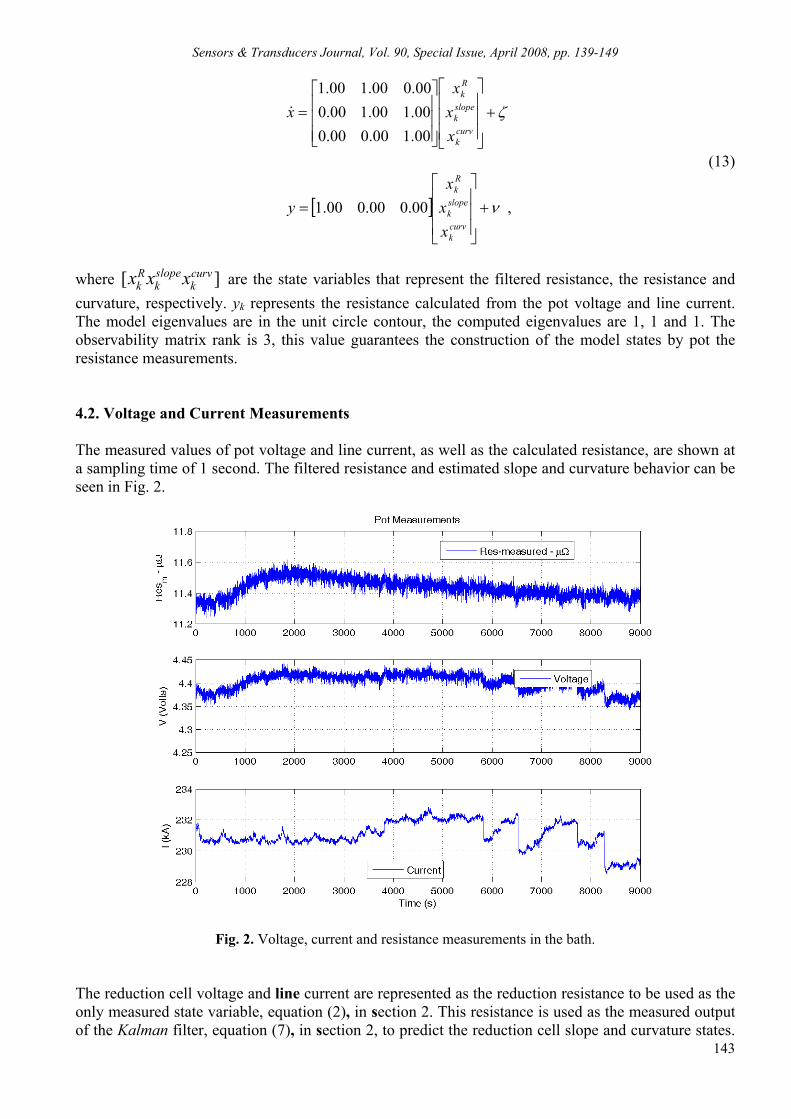
Sensors & Transducers Journal, Vol. 90, Special Issue, April 2008, pp. 139-149
143
ζ+⎥⎥⎥
⎦
⎤
⎢⎢⎢
⎣
⎡
⎥⎥⎥
⎦
⎤
⎢⎢⎢
⎣
⎡=
curvk
slopek
Rk
xxx
x00.100.000.000.100.100.000.000.100.1
&
[ ] ν+⎥⎥⎥
⎦
⎤
⎢⎢⎢
⎣
⎡
=curvk
slopek
Rk
xxx
y 00.000.000.1 ,
(13)
where [ ]slopeR curv
k k kx x x are the state variables that represent the filtered resistance, the resistance and curvature, respectively. yk represents the resistance calculated from the pot voltage and line current. The model eigenvalues are in the unit circle contour, the computed eigenvalues are 1, 1 and 1. The observability matrix rank is 3, this value guarantees the construction of the model states by pot the resistance measurements. 4.2. Voltage and Current Measurements The measured values of pot voltage and line current, as well as the calculated resistance, are shown at a sampling time of 1 second. The filtered resistance and estimated slope and curvature behavior can be seen in Fig. 2.
Fig. 2. Voltage, current and resistance measurements in the bath. The reduction cell voltage and line current are represented as the reduction resistance to be used as the only measured state variable, equation (2), in section 2. This resistance is used as the measured output of the Kalman filter, equation (7), in section 2, to predict the reduction cell slope and curvature states.

Sensors & Transducers Journal, Vol. 90, Special Issue, April 2008, pp. 139-149
144
A statistical analysis of the incoming inputs (voltage and current) and calculated resistance helps to understand the distribution of the values around the mean, and it is useful to understand the nature of the variations during the different stages of the normal operation. The computed resistance and measured signals means, deviation, maximums and minimums, Table 1, and related with its time behavior. As can be observed, the pot is working under normal operational conditions.
Table 1. Resistance, Voltage and Current Statistics.
Measurements Resistance Voltage Current
µΩ V kA Mean 11.4421 4.3687 227.991 Max 11.627 4.423 233.542 Min 11.159 4.273 220.677 Std 0.083 0.0248 1.279 Cov 0.007 0.0006 1.637
The pot operation mode, Fig. 3, and histograms, Fig. 4, reflects the resistance behaviour during different feed control.
Fig. 3. Reduction Cell Status of Operation. 4.3. Gains Adjustment A procedure to tune the Kalman filter gains is based on duality relation, equation (12), following the guidelines suggested by [2], and afterwards it is compared with other digital filter implementations. The variations matrices are associated with the bandwidth of Kalman’s filter and its stability. The procedure strategy is based on the functional mapping,
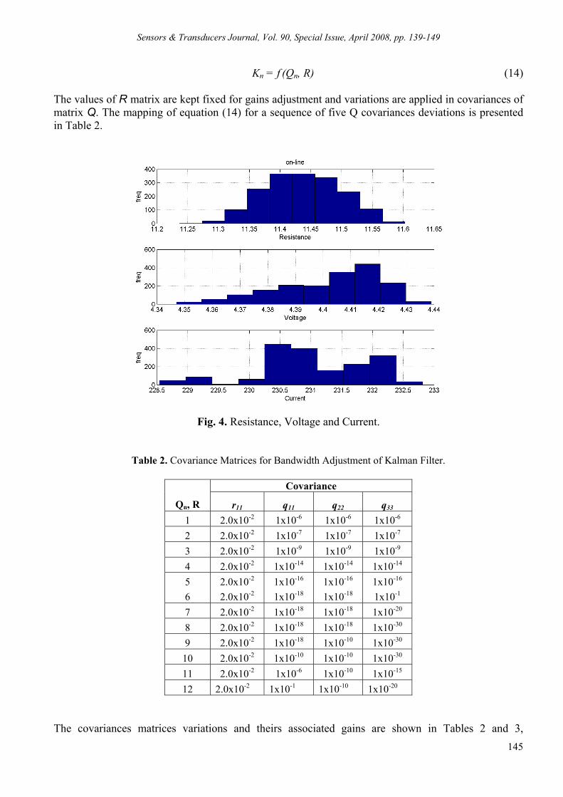
Sensors & Transducers Journal, Vol. 90, Special Issue, April 2008, pp. 139-149
145
Kn = f (Qn, R) (14) The values of R matrix are kept fixed for gains adjustment and variations are applied in covariances of matrix Q. The mapping of equation (14) for a sequence of five Q covariances deviations is presented in Table 2.
Fig. 4. Resistance, Voltage and Current.
Table 2. Covariance Matrices for Bandwidth Adjustment of Kalman Filter.
Covariance
Qn, R r11 q11 q22 q33 1 2.0x10⁻² 1x10⁻⁶ 1x10⁻⁶ 1x10⁻⁶ 2 2.0x10⁻² 1x10⁻⁷ 1x10⁻⁷ 1x10⁻⁷ 3 2.0x10⁻² 1x10⁻⁹ 1x10⁻⁹ 1x10⁻⁹ 4 2.0x10⁻² 1x10-14 1x10-14 1x10-14 5 2.0x10⁻² 1x10-16 1x10-16 1x10-16 6 2.0x10⁻² 1x10-18 1x10-18 1x10⁻¹ 7 2.0x10⁻² 1x10-18 1x10-18 1x10-20 8 2.0x10⁻² 1x10-18 1x10-18 1x10-30 9 2.0x10⁻² 1x10-18 1x10⁻¹⁰ 1x10-30
10 2.0x10⁻² 1x10⁻¹⁰ 1x10⁻¹⁰ 1x10-30 11 2.0x10⁻² 1x10⁻⁶ 1x10⁻¹⁰ 1x10-15 12 2.0x10⁻² 1x10⁻¹ 1x10⁻¹⁰ 1x10-20
The covariances matrices variations and theirs associated gains are shown in Tables 2 and 3,

Sensors & Transducers Journal, Vol. 90, Special Issue, April 2008, pp. 139-149
146
respectively. The filter’s gains are evaluated considering a mapping f(Q; R)→KK, the stochastic matrices spaces Q3x3 and R1x1 are mapped into K3 Kalman gain.
Table 3. Kalman Filter Gains.
Kn GAINS
Qn, R K1 K2 K3 1 7.9390 x10⁻² 3.3170 x10⁻³ 6.7846 x10⁻⁵ 2 5.4792 x10⁻² 1.5545 x10⁻³ 2.1739 x10⁻⁵ 3 2.5815 x10⁻² 3.3867 x10⁻⁴ 2.2070 x10⁻⁶ 4 3.8314 x10⁻³ 7.3575 x10⁻⁶ 7.0575 x10⁻⁹ 5 1.7835 x10⁻³ 1.5906 x10⁻⁶ 7.0756 x10⁻¹⁰ 6 1.0302 x10⁻³ 4.8365 x10⁻⁷ 1.0014 x10⁻¹⁰ 7 9.9985 x10⁻⁴ 4.4470 x10⁻⁷ 8.2456 x10⁻¹¹ 8 9.9953 x10⁻⁴ 4.4429 x10⁻⁷ 8.2272 x10⁻¹¹ 9 1.3716 x10⁻³ 9.2155 x10⁻⁷ 1.2745 x10⁻¹⁰
10 1.3716 x10⁻³ 9.2155 x10⁻⁷ 1.2745 x10⁻¹⁰ 11 2.6494 x10⁻³ 3.5128 x10⁻⁶ 2.2332 x10⁻⁹ 12 2.2552 x10⁻² 1.0026 x10⁻⁵ 1.6729 x10⁻⁹
The SKF bandwidth variations and the time response are analyzed for the five Kalman gains adjustments are presented in Table 3 and are associated with Figs. 5, 6 and 7.
Fig. 5. Case 12 - Estimated Slope of the Reduction Cell. Observing Figs. 5 and 6, we note that bandwidth is reduced as the Q matrix has its eigenvalues tending to zero, Table 2. Consequently, provokes the attenuation of the high frequencies behaviors. Comparing the SKF filter estimation with the parabolic filter in Figs. 5 and 6, we observe that SKF is able to reproduce. The same behavior of the comparison filters by the adjustment of matrices Q and R.
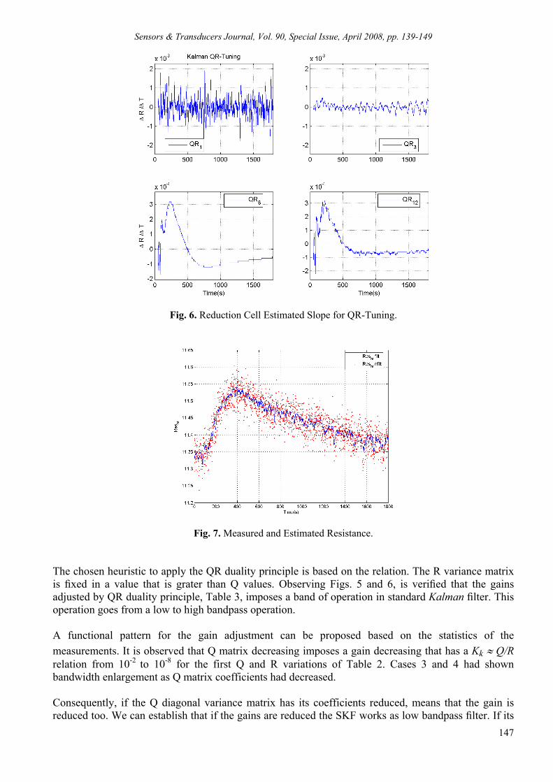
Sensors & Transducers Journal, Vol. 90, Special Issue, April 2008, pp. 139-149
147
Fig. 6. Reduction Cell Estimated Slope for QR-Tuning.
Fig. 7. Measured and Estimated Resistance. The chosen heuristic to apply the QR duality principle is based on the relation. The R variance matrix is fixed in a value that is grater than Q values. Observing Figs. 5 and 6, is verified that the gains adjusted by QR duality principle, Table 3, imposes a band of operation in standard Kalman filter. This operation goes from a low to high bandpass operation. A functional pattern for the gain adjustment can be proposed based on the statistics of the measurements. It is observed that Q matrix decreasing imposes a gain decreasing that has a Kk ≈ Q/R relation from 10-2 to 10-8 for the first Q and R variations of Table 2. Cases 3 and 4 had shown bandwidth enlargement as Q matrix coefficients had decreased. Consequently, if the Q diagonal variance matrix has its coefficients reduced, means that the gain is reduced too. We can establish that if the gains are reduced the SKF works as low bandpass filter. If its
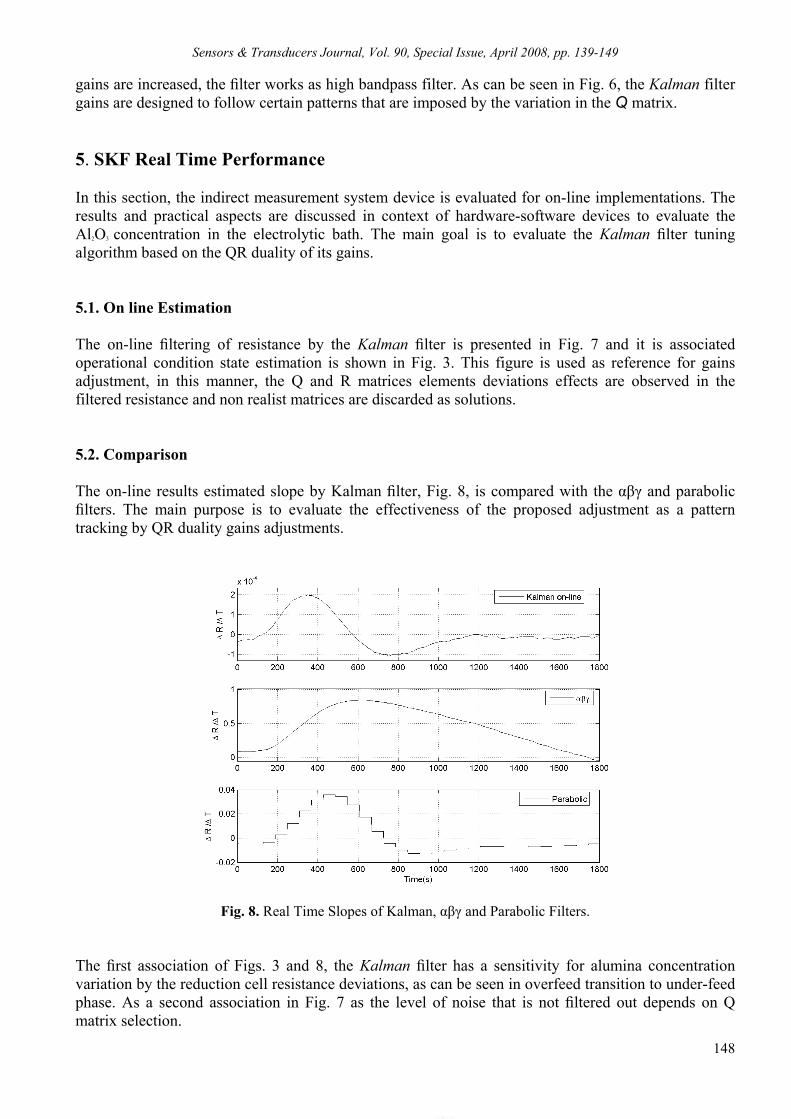
Sensors & Transducers Journal, Vol. 90, Special Issue, April 2008, pp. 139-149
148
gains are increased, the filter works as high bandpass filter. As can be seen in Fig. 6, the Kalman filter gains are designed to follow certain patterns that are imposed by the variation in the Q matrix. 5. SKF Real Time Performance In this section, the indirect measurement system device is evaluated for on-line implementations. The results and practical aspects are discussed in context of hardware-software devices to evaluate the Al2O3 concentration in the electrolytic bath. The main goal is to evaluate the Kalman filter tuning algorithm based on the QR duality of its gains. 5.1. On line Estimation The on-line filtering of resistance by the Kalman filter is presented in Fig. 7 and it is associated operational condition state estimation is shown in Fig. 3. This figure is used as reference for gains adjustment, in this manner, the Q and R matrices elements deviations effects are observed in the filtered resistance and non realist matrices are discarded as solutions. 5.2. Comparison The on-line results estimated slope by Kalman filter, Fig. 8, is compared with the αβγ and parabolic filters. The main purpose is to evaluate the effectiveness of the proposed adjustment as a pattern tracking by QR duality gains adjustments.
Fig. 8. Real Time Slopes of Kalman, αβγ and Parabolic Filters. The first association of Figs. 3 and 8, the Kalman filter has a sensitivity for alumina concentration variation by the reduction cell resistance deviations, as can be seen in overfeed transition to under-feed phase. As a second association in Fig. 7 as the level of noise that is not filtered out depends on Q matrix selection.

Sensors & Transducers Journal, Vol. 90, Special Issue, April 2008, pp. 139-149
149
6. Concluding Remarks In this article it was presented a Kalman filtering bandwidth tuning procedure, based on QR matrices duality principle, for indirect measurement of Al2O3 concentration in the electrolytic bath. Specifically, the main goal was the indirect measurement of the Al2O3 concentration in reduction cell by deviations on the reduction cell resistance. This research results had been applied to a real reduction cells. It focuses the use of the QR duality principle as a design framework for Kalman filter gain adjustment. The framework succeeds in the determination of trial and error heuristic. The improvement of the framework performance can be done by the inclusion of genetic algorithms for the Q and R searches and a Bayesian inference engine. Likewise, the development of neural networks to solve the algebraic Riccati equation for multivariable stochastic state space observers, as an alternative way to by pass the inverse problem computation due to multiple outputs. Also, a metaheuristic and evolutionary algorithms can be s consider to help the tuning of the Kalman filter gains. The proposed method had proven to be good alternative to make the gain adjustment of Kalman when it is used for the indirect measurement of Al2O3 concentration. Especially good is its flexibility on patterns tracking, based on the covariances matrices estimation for the bandwidth adjustment and to improve transient response. In addition to this, the robustness of the filter had been kept along various stages of the normal pot operation, in counterpoint to others filtering methods that have been used widely in the aluminium industry. References [1]. P. C. A. B. J. W. Fiona, Stevens McFaden, Geoffrey P. Bearne, Application of Advance Process Control to
Aluminium Reduction Cell – A Review, 2001, p. 1233. [2]. H.-G. Yeh, Real-Time Implementation of a Narrow-Band Kalman Filter With a Floating- Point Processor
DSP-32, IEEE Transaction on Industrial Electronics, 31, 9, 1990, pp. 13–18. [3]. E. A. S. P. Borg, Dynamic Model and Estimator for Online Supervision of the Alumina Reduction Cell, 08,
1988. [4]. S. M. Bozic. Digital and Kalman Filtering, Edward Arnold, London, 1st edition, 1984. [5]. G. N. S. Pasupathy, Adaptative Estimation of Noise Covariance Matrices in Real-Time Preprocessing of
Geophysical Data, IEEE 05, IEEE, 1997. [6]. S J Kwon, Robust Kalman Filtering with perturbation Estimation Process doe uncertain Systems. IEE
Proceedings, 2006. [7]. J. de Jesus Barros, State Space Estimation of the Sonda Rockets Impact Points., Estimação no Espaço de
Estado do Ponto de Impacto de Foguetes, Master thesis in Portuguese- Dissertação de mestrado, Universidade Federal do Maranhão, São Luís-MA-Brasil, 2005.
[8]. G. C. C. K. Chui, A Modified Adaptative Kalman Filter for Real-Time Applications, IEEE 06, IEEE, 1991. [9]. João Viana DA Fonseca Neto, Carlos. Braga. Nilton F. Nagen, Jorge A. Farid and Fábio Nogueira da Silva,
Bandwidth Adjustment of Digital Kalman Filter for Indirect Measurement of Electrolytic Bath State Variables, 2nd International Conference on Sensing Technology 2007, November 26-28, 2007 at Palmerston North, New Zealand.
___________________
2008 Copyright ©, International Frequency Sensor Association (IFSA). All rights reserved. (http://www.sensorsportal.com)

Sensors & Transducers Journal, Vol. 90, Special Issue, April 2008, pp. 150-159
150
SSSeeennnsssooorrrsss &&& TTTrrraaannnsssddduuuccceeerrrsss
ISSN 1726-5479© 2008 by IFSA
http://www.sensorsportal.com
Signal Processing for the Impedance Measurement on an Electrochemical Generator
El-Hassane AGLZIM, Amar ROUANE, Mustapha NADI
and Djilali KOURTICHE LIEN, Nancy Université, Boulevard des Aiguillettes, BP239 54506 Vandoeuvre lès Nancy - France
E-mail: [email protected]
Received: 15 October 2007 /Accepted: 20 February 2008 /Published: 15 April 2008 Abstract: Improving the life time of batteries or fuel cells requires the optimization of components such as membranes and electrodes and enhancement of the flow of gases [1], [2]. These goals could be reached by using a real time measurement on loaded generator. The impedance spectroscopy is a new way that was recently investigated. In this paper, we present an electronic measurement instrumentation developed in our laboratory to measure and plot the impedance of a loaded electrochemical generator like batteries and fuel cells. Impedance measures were done according to variations of the frequency in a larger band than what is usually used. The electronic instrumentation is controlled by Hpvee® software which allows us to plot the Nyquist graph of the electrochemical generator impedance. The theoretical results obtained in simulation under Pspice® confirm the choice of the method and its advantage. For safety reasons, the experimental preliminary tests were done on a 12 V vehicle battery, having an input current of 330 A and a capacity of 40 Ah and are now extended to a fuel cell. The results were plotted at various nominal voltages of the battery (12.7 V, 10 V, 8 V and 5 V) and with two imposed currents (0.6 A and 4 A).The Nyquist diagram resulting from the experimental data enable us to show an influence of the load of the battery on its internal impedance. The similitude in the graph form and in order of magnitude of the values obtained (both theoretical and practical) enables us to validate our electronic measurement instrumentation. Different sensors (temperature, pressure) were placed around the device under test (DUT). These influence parameters were permanently recorded. Results presented here concern a classic loaded 12 V vehicle battery. The Nyquist diagram resulting from the experimental data confirms the influence of the load of the DUT on its internal impedance. Copyright © 2008 IFSA. Keywords: Fuel cell on load, Impedance Spectroscopy method, Impedance measurement, Nyquist graph.

Sensors & Transducers Journal, Vol. 90, Special Issue, April 2008, pp. 150-159
151
1. Introduction Energy and climate perturbations are now well established challenges. The use of hydrogen in fuel cell is an essential vector, and has been the focus of intensive study in recent years as promising alternative energy sources. Thus, various studies have been carried out in the electronic-physic fields of these kinds of generator [1] [2]. The improvement of the effectiveness and the life time of fuel cells require to optimize components such as membranes and electrodes as well as to enhance the fluid exchanges process. Impedance measurement is a possible metrological tool for this kind of characterizations. It’s a powerful technique, which can provide useful information on the electro-chemical systems in a real and very short time [3]. This technique can be considered as a good tool to determine the status of charge of batteries or fuel cells. Impedance measurement on a battery or fuel cell must be done on a load. This is necessary in order to evaluate the performances in real conditions. Fuel cell components that can affect the impedance include current collectors, porous electrodes, the catalytic layer and the membrane [4]. We are interested in developing a real time diagnostic based on impedance measurement of a battery or fuel cell on load. The method is based on the impedance spectroscopy (EIS) of battery or fuel cell from which the Nyquist diagram is plotted. The analysis and the shape of the diagram can provide information to follow the generator performances on a load. This approach may help in identifying many characteristics of the system as well as the kinetic resistances, the ohmic resistances, the electrolytic, contact and porous layer resistances or the transport limitations of the reactant [3]. The environmental measurement is essential; it allows us to know at what state the impedance measurement was made. To achieve this, several sensors, like temperature, pressure, current, flow of gases, and more sensors recover data and measurements of the DUT. 2. Theoretical Study 2.1. Method A simulation test under Pspice® was done in order to validate the choice of the method and its ability to provide some accurate and exploitable results. The electrochemical generator is represented by an electronic model given in Fig. 1. The variable load is represented by a MOSFET, and the internal impedance of the DUT is represented by Randle’s circuit (Rohm = 10 mΩ, Ract = 90 mΩ, and Cdc = 300 µF). These values correspond to what one can expect for a PEM fuel cell. These estimated values are based on the work carried out by Noponen [5], Wagner [6], Brunetto and al. [7]. They have done measurement on PEMFC with the same dimensions as our fuel cell on which the experimental measurements are expected to be done. They found that the real part is ranging from 3 mΩ and 200 mΩ and the imaginary part is close to 15 mΩ.
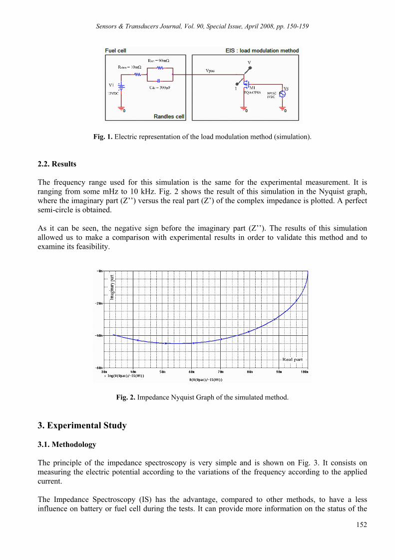
Sensors & Transducers Journal, Vol. 90, Special Issue, April 2008, pp. 150-159
152
Fig. 1. Electric representation of the load modulation method (simulation). 2.2. Results The frequency range used for this simulation is the same for the experimental measurement. It is ranging from some mHz to 10 kHz. Fig. 2 shows the result of this simulation in the Nyquist graph, where the imaginary part (Z’’) versus the real part (Z’) of the complex impedance is plotted. A perfect semi-circle is obtained. As it can be seen, the negative sign before the imaginary part (Z’’). The results of this simulation allowed us to make a comparison with experimental results in order to validate this method and to examine its feasibility.
Fig. 2. Impedance Nyquist Graph of the simulated method. 3. Experimental Study 3.1. Methodology The principle of the impedance spectroscopy is very simple and is shown on Fig. 3. It consists on measuring the electric potential according to the variations of the frequency according to the applied current. The Impedance Spectroscopy (IS) has the advantage, compared to other methods, to have a less influence on battery or fuel cell during the tests. It can provide more information on the status of the

Sensors & Transducers Journal, Vol. 90, Special Issue, April 2008, pp. 150-159
153
charge. Measurements are generally carried out without load. It is useful to cover a large frequency range in order to obtain more information from the impedance spectrum generated. For a Proton Exchange Membrane Fuel Cell (PEMFC), the impedance spectrum was generated in a frequency ranging from 1 Hz to 10 kHz [8]. However, Walkiewicz et al [9] did studies between 1 mHz and 65 KHz. The number of points collected by decade varies between 8 and 10 points. The principle of measurement is to add a signal, at constant frequency, to the output of the voltage of the battery when it is delivering the desired current. The superimposed signal can be obtained by three methods: potentiostatic, galvanostatic or load modulation method. Among these three methods, we have selected the load modulation method. It consists in varying the resistance of the load according to the signal that we would like to superimpose. Thus, the impedance of the generator under test can be obtained by the ratio of the voltage of the battery and the current coming from the battery. Fig. 3 shows an electric diagram of this method.
Fig. 3. Electric representation of the load modulation method [10].
3.2. Principle of the Electronic Measurement Instrumentation The principle of the electronic instrumentation is presented in Fig. 4. The current is controlled by an analogical current regulation. This choice allows us to have a more linear, fast and reliable regulation. The instrumentation uses a VXI system stand, which controls different electronic cards. Software, under Hpvee®, was developed for automatic impedance measurements of the DUT. Two synchronous detections were used to filter the noise and reject the 50Hz. They filter a very narrow band around the processed voltage and current signals. Thus, it is possible to filter all the noise and to detect the amplitude of the useful signal at frequency fixed. These two synchronous detectors are controlled by four square signals for which the differences in phase are 90°. The real and imaginary parts of the DUT impedance are deduced from their outputs by simply using Ohm’s law. These two parameters (real and imaginary part of the complex impedance) are then plotted in the Nyquist diagram. The instrumentation is controlled by dedicated Hpvee® software. This software controls a VXI system stand containing several measuring devices in the form of plug-in circuits: a low frequency generator (HPE1340A), a multimeter (HPE1326B), a 4-Channel D/A Converter (HPE1328A), a 16 ways multiplexer (HPE1351A) and an input/output circuit (HPE1330B). The instrumentation is composed of six modules. Each module provides signals to the other for an automatic measurement. This modular approach is for the prototype development and will be integrated in one specific card at the end. The card can then be integrated within a vehicle as an embedded system.

Sensors & Transducers Journal, Vol. 90, Special Issue, April 2008, pp. 150-159
154
Fig. 4. Principle of the electronic measurement instrumentation. The “Power supply” module provides the supply to the various electronic circuits, it delivers a tension of +/-13 V and +/-7.5 V. The “Signals generator” module provides the control square signals for the tension and current synchronous detections, as well as the current imposed signal. These signals are generated from the sinusoidal signal delivered by a GBF. The frequency scanning is controlled by the Hpvee® program, which changes the frequency value step by step. The “Current control” module drives the load by an imposed current while running. This current is a square signal, generated by the “Signals generator” module; it is composed of a DC part which represent the imposed current and an AC part which represents the frequency on which this current is imposed. The “Amplification” module amplifies the imposed current signal, measured at the Shunt resistance terminals. This amplified signal, which is disturbed, is transmitted to the synchronous detection (current). The “Synchronous detection” module allows the amplification of the signal coming from the DUT, and the recovery of the real and imaginary part of this signal by the synchronous detection. To test the system, we have developed a load which can support current up to 50 A (Fig. 5). All the systems surrounding, as GBF, the computer, the oscilloscope or multimeters, will be replaced in a more evolved version of the instrumentation by components able to provide the same functionalities. 4. Results and Discussion In order to avoid any risk for the fuel cell, preliminary results have been carried out on a classical (and cheaper) 12 V vehicle battery delivering a starting current of 330 A and having a capacity of 40 Ah. The impedance spectrum of a fuel cell and a vehicle battery are very close because the electrochemical processes are almost identical [11] [12]. However, spectrums are very depending on the values of components used in the Randles model. [13]. Measurements were carried out at different nominal voltages (12.7 V, 10 V, 8 V and 5 V) with two imposed currents (0.6 A and 4 A). The choice of these limits current is arbitrary. Fig. 7 and 8 show the complex plane impedance plots (Nyquist diagram) carried out with the electronic instrumentation. Fig. 9 show the complex plane impedance plots carried out with the N3301A Agilent load [8] at a nominal voltage of 12.7 V. The results obtained enable us to show the influence of the load on its impedance. Nyquist Graphs showed below were obtained by using the Hpvee® software developed for the opportunity, it is then transposed under Microsoft® Excel in order to plot the curves. Nyquist graphs are generally presented in the literature have a positive imaginary axis. Actually, values on the axis of the imaginary part are negative (capacitor effect), but by convention, when the graph is plotted, they are multiplied by -1.
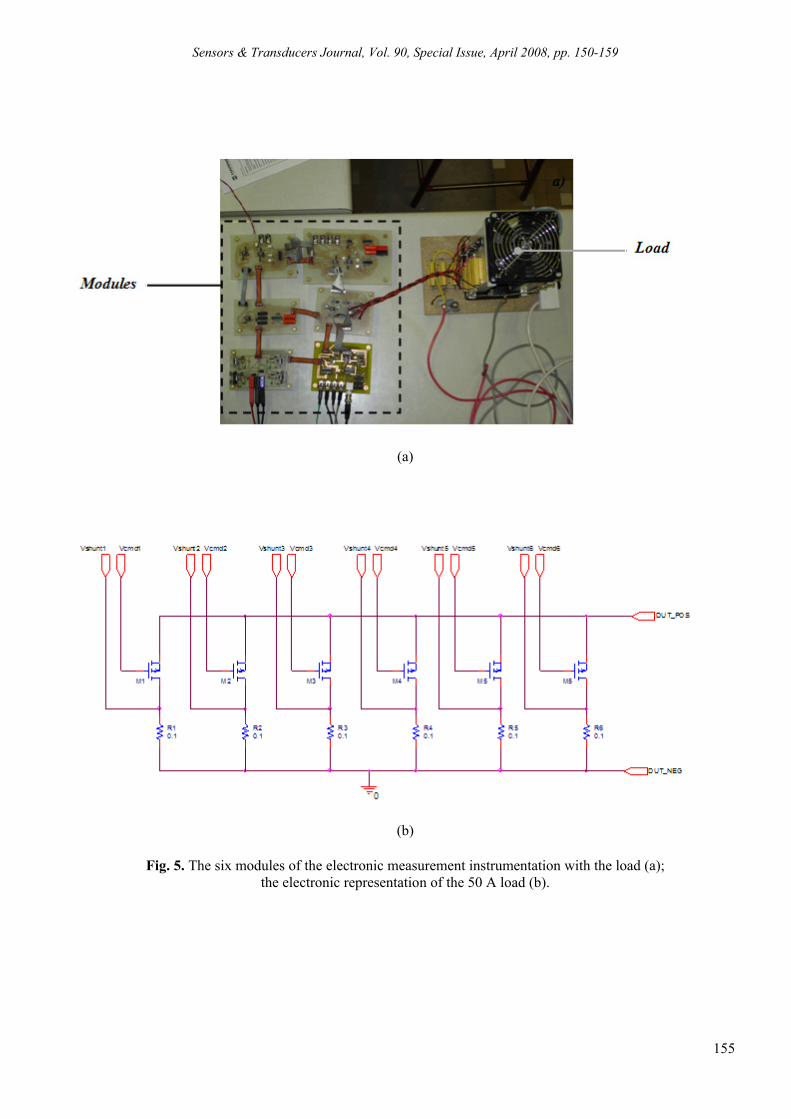
Sensors & Transducers Journal, Vol. 90, Special Issue, April 2008, pp. 150-159
155
(a)
(b)
Fig. 5. The six modules of the electronic measurement instrumentation with the load (a); the electronic representation of the 50 A load (b).

Sensors & Transducers Journal, Vol. 90, Special Issue, April 2008, pp. 150-159
156
Fig. 6. An overall view of the electronic measurement instrumentation.
Fig. 7. Impedance of the battery at an imposed current of 0.6 A and at different nominal voltages
The impedance is carried out with the electronic measurement instrumentation.
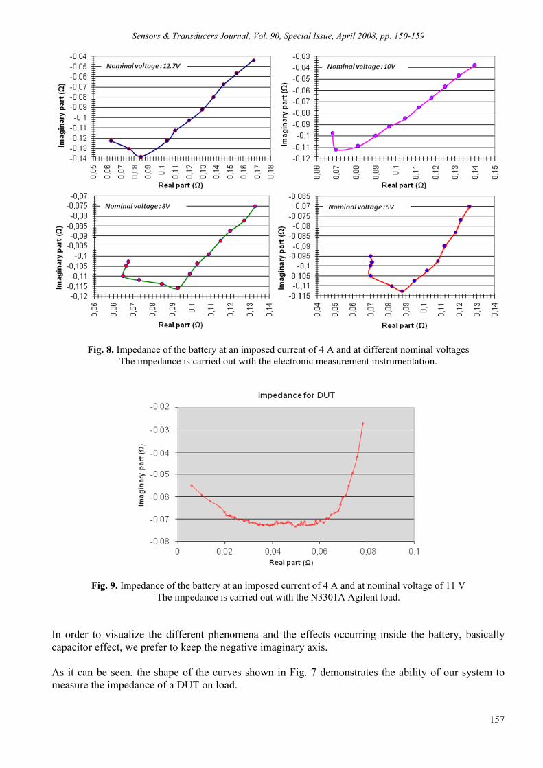
Sensors & Transducers Journal, Vol. 90, Special Issue, April 2008, pp. 150-159
157
Fig. 8. Impedance of the battery at an imposed current of 4 A and at different nominal voltages The impedance is carried out with the electronic measurement instrumentation.
Fig. 9. Impedance of the battery at an imposed current of 4 A and at nominal voltage of 11 V The impedance is carried out with the N3301A Agilent load.
In order to visualize the different phenomena and the effects occurring inside the battery, basically capacitor effect, we prefer to keep the negative imaginary axis. As it can be seen, the shape of the curves shown in Fig. 7 demonstrates the ability of our system to measure the impedance of a DUT on load.
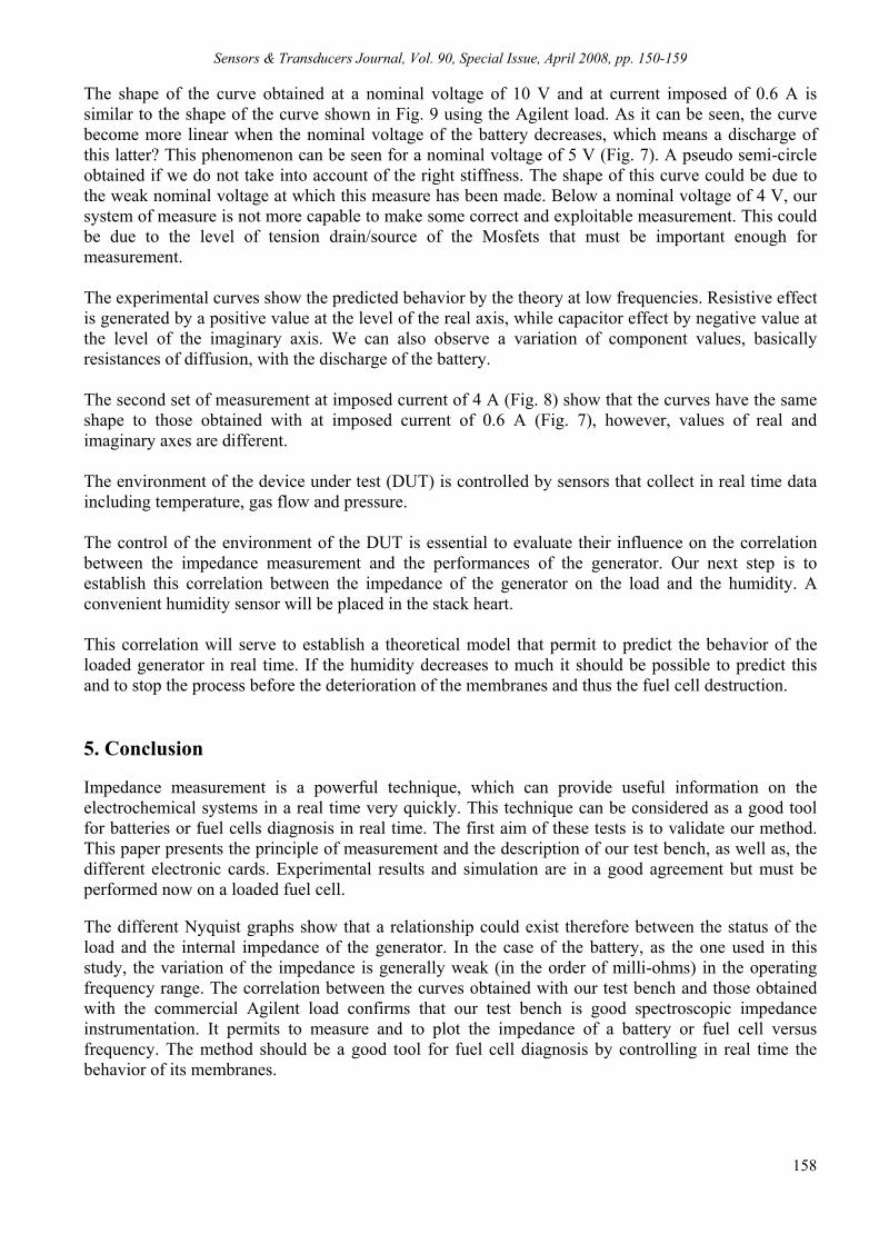
Sensors & Transducers Journal, Vol. 90, Special Issue, April 2008, pp. 150-159
158
The shape of the curve obtained at a nominal voltage of 10 V and at current imposed of 0.6 A is similar to the shape of the curve shown in Fig. 9 using the Agilent load. As it can be seen, the curve become more linear when the nominal voltage of the battery decreases, which means a discharge of this latter? This phenomenon can be seen for a nominal voltage of 5 V (Fig. 7). A pseudo semi-circle obtained if we do not take into account of the right stiffness. The shape of this curve could be due to the weak nominal voltage at which this measure has been made. Below a nominal voltage of 4 V, our system of measure is not more capable to make some correct and exploitable measurement. This could be due to the level of tension drain/source of the Mosfets that must be important enough for measurement. The experimental curves show the predicted behavior by the theory at low frequencies. Resistive effect is generated by a positive value at the level of the real axis, while capacitor effect by negative value at the level of the imaginary axis. We can also observe a variation of component values, basically resistances of diffusion, with the discharge of the battery. The second set of measurement at imposed current of 4 A (Fig. 8) show that the curves have the same shape to those obtained with at imposed current of 0.6 A (Fig. 7), however, values of real and imaginary axes are different. The environment of the device under test (DUT) is controlled by sensors that collect in real time data including temperature, gas flow and pressure. The control of the environment of the DUT is essential to evaluate their influence on the correlation between the impedance measurement and the performances of the generator. Our next step is to establish this correlation between the impedance of the generator on the load and the humidity. A convenient humidity sensor will be placed in the stack heart. This correlation will serve to establish a theoretical model that permit to predict the behavior of the loaded generator in real time. If the humidity decreases to much it should be possible to predict this and to stop the process before the deterioration of the membranes and thus the fuel cell destruction. 5. Conclusion Impedance measurement is a powerful technique, which can provide useful information on the electrochemical systems in a real time very quickly. This technique can be considered as a good tool for batteries or fuel cells diagnosis in real time. The first aim of these tests is to validate our method. This paper presents the principle of measurement and the description of our test bench, as well as, the different electronic cards. Experimental results and simulation are in a good agreement but must be performed now on a loaded fuel cell. The different Nyquist graphs show that a relationship could exist therefore between the status of the load and the internal impedance of the generator. In the case of the battery, as the one used in this study, the variation of the impedance is generally weak (in the order of milli-ohms) in the operating frequency range. The correlation between the curves obtained with our test bench and those obtained with the commercial Agilent load confirms that our test bench is good spectroscopic impedance instrumentation. It permits to measure and to plot the impedance of a battery or fuel cell versus frequency. The method should be a good tool for fuel cell diagnosis by controlling in real time the behavior of its membranes.

Sensors & Transducers Journal, Vol. 90, Special Issue, April 2008, pp. 150-159
159
Acknowledgements The Authors would like to thank the Lorraine region – France – for supporting this work. References [1]. E. Bradley Easton, Peter G. Pickup, An electrochemical impedance spectroscopy study of fuel cell
electrodes, Electrochimica Acta, 50, 2005, pp. 2469–2474. [2]. P. Jasinski, T. Suzuki, F. Dogan, H.U. Anderson, Impedance spectroscopy of single chamber SOFC, Solid
State Ionics, 175, 2004, pp. 35–38. [3]. Guangchun Li, Peter G. Pickup, Measurement of single electrode potentials and impedances in hydrogen
and direct methanol PEM fuel cells, Electrochimica Acta, 49, 2004, pp. 4119–4126. [4]. M. Smith, K. Cooper, D. Johnson, L. Scribner, Comparison of Fuel Cell Electrolyte – Resistance
Measurement Techniques, The Magazine of Fuel Cell Business and Technology, 2005. [5]. Matti Noponen, Current Distribution measurements and Modeling of Mass Transfer in Polymer Electrolyte
Fuel Cells, PhD thesis, Helsinki University of Technology, Laboratory of Advanced Energy Systems, Department of Engineering Physics and Mathematics, 2004.
[6]. N. Wagner, Characterization of membrane electrode assemblies in polymer electrolyte fuel cells using AC impedance spectroscopy, Journal of Applied Electrochemistry, 32, 2002, pp. 589–863.
[7]. C. Brunetto, G. Tina, G. Squadrito and A. Moschetto, PEMFC Diagnostics and Modeling by Electrochemical Impedance Spectroscopy, IEEE MELECON, 3, 2004, pp. 1045–1050.
[8]. Agilent Technologies, Making Fuel Cell AC Impedance Measurements Utilizing Agilent N3300A Series Electronic Loads, Product Note, 2002.
[9]. S. Walkiewicz, Étude par spectroscopie d’impédance électrochimique de piles à combustibles à membrane échangeuse de protons, DEA Électrochimie, Institut National Polytechnique de Grenoble ENSEEG, 2001.
[10]. B. Kraemer, Mesure par spectroscopie de l’impédance d’une pile à combustible en charge, rapport de DEA, UHP Nancy1, 2005.
[11]. J. P. Diard, B. Le Gorrec, C. Montella, C. Poinsignon and G. Vitter, Impedance Measurements of Polymer Electrolyte Membrane Fuel Cells Running on Constant Load, Journal of Power Sources, 74, 1998, pp. 244–245.
[12]. J. P. Diard, B. Le Gorrec and C. Montella, EIS Study of Electrochemical Battery discharge on constant load, Journal of Power Sources, 70, 1998, pp. 78–84.
[13]. Jörn A. Tinnemeyer, Multiple Model Impedance Spectroscopy Techniques for testing Electrochemical Systems, Journal of Power Sources, 136, 2004, pp. 246–249.
___________________
2008 Copyright ©, International Frequency Sensor Association (IFSA). All rights reserved. (http://www.sensorsportal.com)
Sensors & Transducers Journal, Vol. 90, Special Issue, April 2008, pp. 160-173
160
SSSeeennnsssooorrrsss &&& TTTrrraaannnsssddduuuccceeerrrsss
ISSN 1726-5479© 2008 by IFSA
http://www.sensorsportal.com
Gas Sensing Performance of Pure and Modified BST Thick Film Resistor
*1G. H. JAIN, 2V. B. GAIKWAD, 1D. D. KAJALE, 2R. M. CHAUDHARI,
2R. L. PATIL, 3N. K. PAWAR, 1M. K. DEORE, 2S. D. SHINDE and 4L. A. PATIL
1Department of Physics, Arts, Commerce and Science College, Nandgaon, India 423 106,
2Department of Chemistry, K. T. H. M. College, Nashik, India 422 002,
3Department of Physics, K.A.A.N.S. Arts, Commerce and Science College, Satana, India, 4Material Science Laboratory, Pratap College,
Amalner, India 425 401 *E-mail: [email protected]
Received: 15 October 2007 /Accepted: 20 February 2008 /Published: 15 April 2008 Abstract: Barium Strontium Titanate (BST-(Ba0.87Sr0.13)TiO3) ceramic powder was prepared by mechanochemical process. The thick films of different thicknesses of BST were prepared by screen-printing technique and gas-sensing performance of these films was tested for various gases. The films showed highest response and selectivity to ammonia gas. The pure BST film was surface modified by surfactant CrO3 by using dipping technique. The surface modified film suppresses the response to ammonia and enhances to H2S gas. The surface modification of films changes the adsorption-desorption relationship with the target gas and shifts its selectivity. The gas response, selectivity, response and recovery time of the pure and modified films were measured and presented. Copyright © 2008 IFSA. Keywords: Barium Strontium Titanate, Thick films, Ammonia gas sensor, H2S gas sensor, Selectivity 1. Introduction The sensors are required basically for measurement of physical quantities and for use of controlling some systems. Presently, the atmospheric pollution has become a global issue. Gases from auto and industrial exhausts are polluting the environment. In order to detect, measure and control these gases,

Sensors & Transducers Journal, Vol. 90, Special Issue, April 2008, pp. 160-173
161
one should know the amount and type of gases present in the ambient. Thus, the need to monitor and control these gases has led to the research and development of a wide variety of sensors using different materials and technologies. Gas sensitive resistors based on semiconducting oxides are simple and robust devices which owe their response to changes in charge-carrier concentration within a depletion layer at the solid-gas interface, in turn caused by a change in the surface density of electron trap states [1, 2]. They raise interesting questions of surface chemistry: the effects are considered due either to change in the surface coverage of the adsorbed oxygen species, caused by a reaction with the gas, or to adsorption of a gas species generating a new surface trap state. Detection of ammonia (NH3) is required in many applications including leak-detection in air conditioning systems [3], sensing of trace amounts in air for environmental analysis [4], breath analysis for medical diagnoses [5], animal housing and more. Generally, because it is toxic, it is required to be able to sense low levels of NH3, but it should also be sensitive to much higher levels. NH3 gas is very corrosive, often causing existing NH3 sensors to suffer from drift, which have short life times. The ammonia sensors that have been manufactured in the largest quantities are mostly based on SnO2 sensors [6-11]. Some of the well-known materials for ammonia sensors are pure ZnO [12, 13], SnO2 [14], TiO2 [15], Cr2O3-doped TiO2 [16], etc. A different approach to make selective metal-oxide gas sensor is by using metals or additives that enhance the chemisorptions of specific gases. WO3 based sensing material is demonstrated to respond to NH3 [17-18]. Very low detection limits of 1 ppm for ammonia sensing have been reported using a WO3 ammonia sensor with Au and MoO3 additives. This sensor is operated at an elevated temperature of more than 400oC [18]. Most sensors have much higher detection limits. Normal detection of these sensors ranges from 1 to 1000 ppm [18, 19]. Another type of widely used ammonia sensor, employing electrolyte solutions with diaphragm electrodes, has major limitations due to the cost of fabrication and its relatively poor sensitivity and selectivity. Similarly, Pd gate metal oxide semiconductor device is also sensitive to ammonia but it does not offer sufficient selectivity, because ammonia is indirectly detected by sensing the hydrogen after decomposition [20]. The pervoskite oxides (ABO3) were used as gas sensor materials for their stability in thermal and chemical atmospheres. So, over a last decade, the pervoskite oxide ceramic such as BaTiO3 [21-24] and (Ba,Sr)TiO3 [25-29] have created and promoted interest in chemical sensors. Modifications in microstructure, processing parameters and also concentration of acceptor/donor dopant can vary the temperature coefficient of the resistance and conductivity of ABO3 oxides. Sensors based on ABO3–type complex oxide material, of rare earth elements have an outstanding merit of its high sensitive and selective characteristics. These characteristics can be controlled by selecting suitable A and B atoms or chemically doping A′ and B′ elements equivalent respectively to A and B into ABO3 to obtain AxA′1-
xByB′1-yO3 compound [30, 31]. Jain and Patil [32] have reported the sensing behaviour of pure and modified (Ba0.67Sr0.33)TiO3, and showed that unmodified and modified (Ba0.67Sr0.33)TiO3 are sensitive to H2S gas. The present work is to explain the gas sensing performance of (Ba0.87Sr0.13)TiO3 (BST) and modified (Ba0.87Sr0.13)TiO3 thick film resistors. In the present study, it has been observed that response to NH3 gas increases with increase in (Ba0.87Sr0.13)TiO3 film thickness up to certain limit, beyond that the response decreases on further increase in thickness. However, Roy et al [29] reported that the NH3 gas response goes on increasing with film thickness. The NH3 gas response varied depending upon the thicknesses, micro-structural variations, operating temperature and the concentration of gas. (Ba0.87Sr0.13)TiO3 thick films were surface modified using chromium trioxide (CrO3) solution by dipping technique. The surface modification shifts the response of (Ba0.87Sr0.13)TiO3 thick film from NH3 to H2S gas.

Sensors & Transducers Journal, Vol. 90, Special Issue, April 2008, pp. 160-173
162
2. Experimental 2.1. Powder Preparation Barium Strontium Titanate (BST-(Ba0.87Sr0.13)TiO3) ceramic powder was prepared by mechanochemical process, explained elsewhere [33]. The XRD spectrum of as prepared powder confirmed the sub microcrystalline pervoskite phase. The composition ratios (Ba/Sr) of the as prepared powder were confirmed using the microarea EDS analysis. 2.2. Preparation of Thick Films The thixotropic paste was formulated by mixing the fine powder of BST with the solution of ethyl cellulose (a temporary binder) in a mixture of organic solvents such as butyl cellulose, butyl carbitol acetate and terpineol etc. The ratio of inorganic part to organic part was kept at 75:25 in formulating the paste. This paste was screen printed [24] on glass substrate in the desired pattern. The films were fired at 550oC for 30min. 2.3. Variation of Thickness The thickness of the films was measured by using the Taylor–Hobson (Talystep, UK) system. The thicknesses of the films were observed in the range from 65–70 mm. The reproducibility in thickness of the films was possible by maintaining proper rheology and thixotropy of the paste. Films of various thicknesses were prepared by controlling the number of impressions of squeeze strokes. Different films of thicknesses: 1BST(17µm), 2BST(33µm), 3BST(48µm) and 4BST(63µm), were printed. The reproducibility in the thickness of the films was possible by maintaining proper rheology and thixotropy of the paste. 2.4. Surface Modification of Films The surface modified 2BST thick films were obtained by dipping them in a 0.1M aqueous solution of chromium trioxide (CrO3) for different intervals of dipping time: 5, 10, 20 and 30min. These films were dried at 80oC, followed by firing at 550oC for 30min. These surface modified films are termed as ‘Cr2O3-modified’ BST films. 2.5. Characterization The structural properties of the powder were studied using a Rigaku model DMAX-2500 X-ray diffractometer (XRD) with Cu-Kα radiation, having λ = 1.5406 Å. The microstructure and chemical compositions of the films were analyzed using a scanning electron microscope (SEM, JEOL JED 6300) coupled with an energy dispersive spectrometer (EDS, JEOL JED2300LA). The thicknesses of the thick films were measured using a Taylor–Hobson (Talystep, UK) system. The sensing performance of the sensors was examined using a ‘static gas sensing system’ explained elsewhere [24].
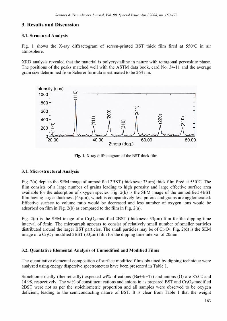
Sensors & Transducers Journal, Vol. 90, Special Issue, April 2008, pp. 160-173
163
3. Results and Discussion 3.1. Structural Analysis Fig. 1 shows the X-ray diffractogram of screen-printed BST thick film fired at 550oC in air atmosphere. XRD analysis revealed that the material is polycrystalline in nature with tetragonal pervoskite phase. The positions of the peaks matched well with the ASTM data book, card No. 34-11 and the average grain size determined from Scherer formula is estimated to be 264 nm.
Fig. 1. X-ray diffractogram of the BST thick film.
3.1. Microstructural Analysis Fig. 2(a) depicts the SEM image of unmodified 2BST (thickness: 33µm) thick film fired at 550oC. The film consists of a large number of grains leading to high porosity and large effective surface area available for the adsorption of oxygen species. Fig. 2(b) is the SEM image of the unmodified 4BST film having larger thickness (63µm), which is comparatively less porous and grains are agglomerated. Effective surface to volume ratio would be decreased and less number of oxygen ions would be adsorbed on film in Fig. 2(b) as compared to the film in Fig. 2(a). Fig. 2(c) is the SEM image of a Cr2O3-modified 2BST (thickness: 33µm) film for the dipping time interval of 5min. The micrograph appears to consist of relatively small number of smaller particles distributed around the larger BST particles. The small particles may be of Cr2O3. Fig. 2(d) is the SEM image of a Cr2O3-modified 2BST (33µm) film for the dipping time interval of 20min. 3.2. Quantative Elemental Analysis of Unmodified and Modified Films The quantitative elemental composition of surface modified films obtained by dipping technique were analyzed using energy dispersive spectrometers have been presented in Table 1. Stoichiometrically (theoretically) expected wt% of cations (Ba+Sr+Ti) and anions (O) are 85.02 and 14.98, respectively. The wt% of constituent cations and anions in as prepared BST and Cr2O3-modified 2BST were not as per the stoichiometric proportion and all samples were observed to be oxygen deficient, leading to the semiconducting nature of BST. It is clear from Table 1 that the weight
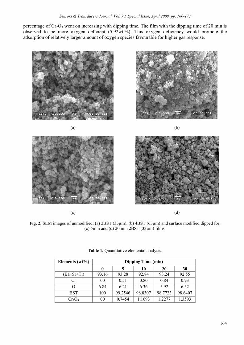
Sensors & Transducers Journal, Vol. 90, Special Issue, April 2008, pp. 160-173
164
percentage of Cr2O3 went on increasing with dipping time. The film with the dipping time of 20 min is observed to be more oxygen deficient (5.92wt.%). This oxygen deficiency would promote the adsorption of relatively larger amount of oxygen species favourable for higher gas response.
(a)
(b)
(c)
(d)
Fig. 2. SEM images of unmodified: (a) 2BST (33µm), (b) 4BST (63µm) and surface modified dipped for: (c) 5min and (d) 20 min 2BST (33µm) films.
Table 1. Quantitative elemental analysis.
Dipping Time (min) Elements (wt%) 0 5 10 20 30
(Ba+Sr+Ti) 93.16 93.28 92.84 93.24 92.55 Cr 00 0.51 0.80 0.84 0.93 O 6.84 6.21 6.36 5.92 6.52
BST 100 99.2546 98.8307 98.7723 98.6407 Cr2O3 00 0.7454 1.1693 1.2277 1.3593

Sensors & Transducers Journal, Vol. 90, Special Issue, April 2008, pp. 160-173
165
3.2. Thermal Analysis Fig. 3 shows the thermogravimetric profile of pure and Cr2O3-modified 2BST films. Table 2 lists loss or gain in weight percentage of pure and Cr2O3-modified 2BST films in the different ranges of temperature observed from TGA. Comparatively a less weight loss and a more gain in the Cr2O3-modified 2BST sample can be attributed to the adsorbed oxygen content. The film with the content of Cr2O3 (1.2277wt%) has been observed to contain the smallest amount of oxygen (5.92wt%, Table 1), which could be attributed to the largest deficiency of oxygen in the film. It is, therefore, quite possible that the material would adsorb the largest possible amount of oxygen, showing a relatively less weight loss. The Cr2O3 on the surface of modified sample would form misfits regions between the grains of BST and could act as an efficient catalyst for oxygenation.
Fig. 3. TGA of pure and Cr2O3-modified 2BST films.
Table 2. Thermal analysis.
Pure 2BST Cr2O3-modified 2BST Temp. (oC) Loss (wt%) Gain (wt%)
Temp. (oC) Loss (wt%) Gain (wt%)
30-25 1.20 -- 30-125 1.0 -- 125-245 -- 1.20 125-245 -- 1.2 245-290 0.20 -- 245-290 0.2 -- 290-340 -- 0.20 290-340 -- 0.4 340-900 2.25 -- 340-900 0.6 --
4. Gas Sensing Performance of Unmodified BST films 4.1. Unmodified BST Films 4.1.1. Gas Response with Operating Temperature Gas response or sensitivity of a sensor is defined as the ratio of the conductance change upon exposure to a test gas to the conductance in air. Fig. 4 shows the variation in NH3 gas (300 ppm) response with operating temperatures (for films of various thicknesses). It is noted from the graph that the response goes on increasing with the increasing temperature, and attains a maximum at 300oC, and decreases with further increase in operating

Sensors & Transducers Journal, Vol. 90, Special Issue, April 2008, pp. 160-173
166
temperature for all thicknesses and film thickness of 33 µm is found to be most sensitive for sensing NH3 gas.
0102030405060708090
100 150 200 250 300 350 400 450Temp(oC)
Gas
resp
onse
1BST(17 µm)2BST(33 µm)3BST(48 µm)4BST(63 µm)
Fig. 4. Variation of NH3 gas response with operating temperature for 300 ppm.
The variation in gas response with film thickness, and the sudden change in response at a particular thickness may be due to optimum porosity. The porosity appears to increase with increasing film thickness. Beyond a certain limit of thickness, the porosity may decrease due to densely populated particles, which could easily agglomerate. The increased porosity could promote the in-pore adsorption of oxygen, which could then improve the adsorption-desorption of the target gas. 4.1.2. Response and Recovery with Gas Concentrations The time taken for the sensor to attain 90% of the maximum change in resistance upon exposure to the gas is the response time. The time taken by the sensor to get back 90% to the original resistance is the recovery time [34]. Fig. 5 shows the response and recovery profiles of the most sensitive unmodified 2BST film to ammonia gas at 300oC, and it is observed that the response and recovery time increase with gas concentration.
Fig. 5. Response speed of the (2BST) film at different NH3 gas concentrations.
NH3 gas
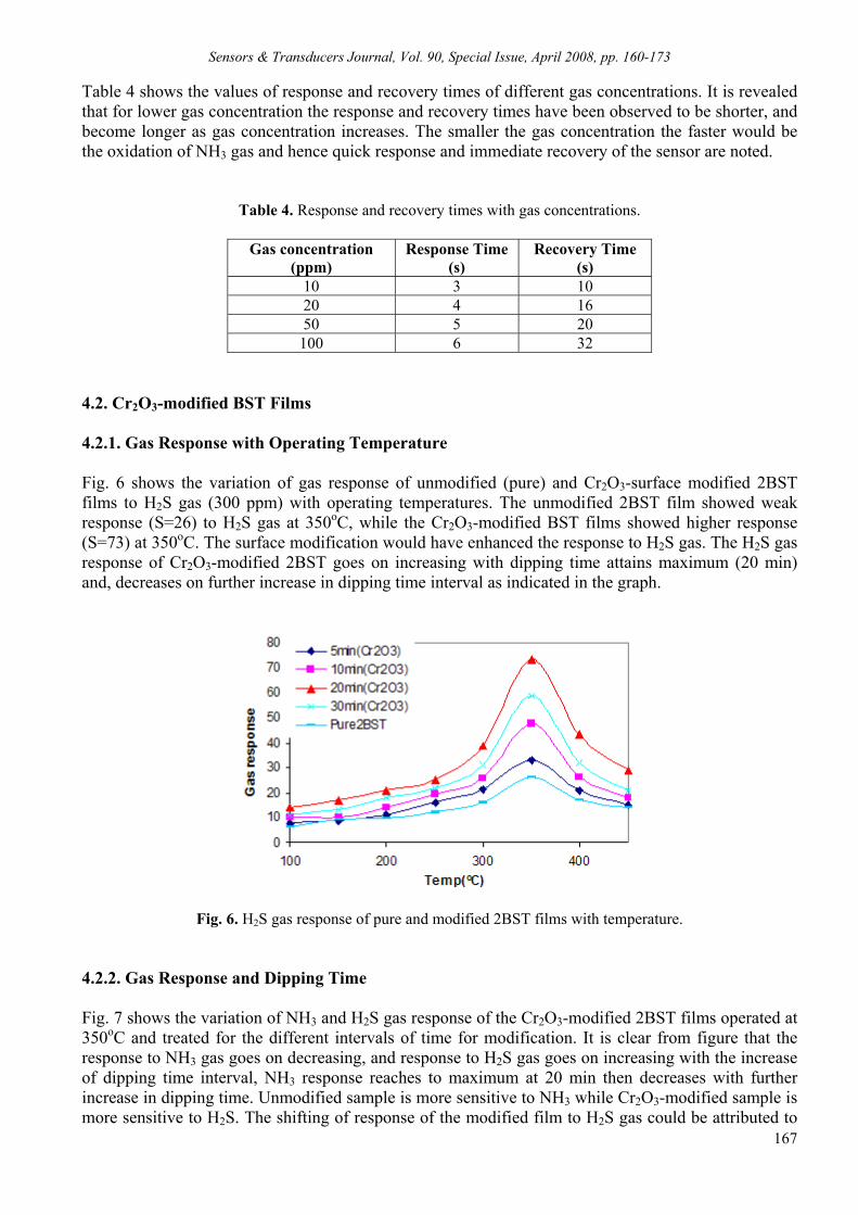
Sensors & Transducers Journal, Vol. 90, Special Issue, April 2008, pp. 160-173
167
Table 4 shows the values of response and recovery times of different gas concentrations. It is revealed that for lower gas concentration the response and recovery times have been observed to be shorter, and become longer as gas concentration increases. The smaller the gas concentration the faster would be the oxidation of NH3 gas and hence quick response and immediate recovery of the sensor are noted.
Table 4. Response and recovery times with gas concentrations.
Gas concentration (ppm)
Response Time (s)
Recovery Time (s)
10 3 10 20 4 16 50 5 20
100 6 32 4.2. Cr2O3-modified BST Films 4.2.1. Gas Response with Operating Temperature Fig. 6 shows the variation of gas response of unmodified (pure) and Cr2O3-surface modified 2BST films to H2S gas (300 ppm) with operating temperatures. The unmodified 2BST film showed weak response (S=26) to H2S gas at 350oC, while the Cr2O3-modified BST films showed higher response (S=73) at 350oC. The surface modification would have enhanced the response to H2S gas. The H2S gas response of Cr2O3-modified 2BST goes on increasing with dipping time attains maximum (20 min) and, decreases on further increase in dipping time interval as indicated in the graph.
Fig. 6. H2S gas response of pure and modified 2BST films with temperature.
4.2.2. Gas Response and Dipping Time Fig. 7 shows the variation of NH3 and H2S gas response of the Cr2O3-modified 2BST films operated at 350oC and treated for the different intervals of time for modification. It is clear from figure that the response to NH3 gas goes on decreasing, and response to H2S gas goes on increasing with the increase of dipping time interval, NH3 response reaches to maximum at 20 min then decreases with further increase in dipping time. Unmodified sample is more sensitive to NH3 while Cr2O3-modified sample is more sensitive to H2S. The shifting of response of the modified film to H2S gas could be attributed to

Sensors & Transducers Journal, Vol. 90, Special Issue, April 2008, pp. 160-173
168
conversion of Cr2O3 into Cr2S3, which is conducting in nature. Surface modification would have altered the adsorbate-adsorbent interactions so as to obtain unusual selectivity and sensitivity effects to H2S gas.
Fig. 7. Variation of NH3 and H2S gas response with dipping time.
4.2.3. Selectivity of Pure and Cr2O3-modified BST Films The ability of a sensor to respond to a certain gas in the presence of other gases is known as selectivity. Fig. 8 shows the histogram of selectivities of the pure and Cr2O3-modified 2BST film. It is clear from the histogram that the pure BST is more selective to NH3 while Cr2O3-modified is more selective to H2S gas. Cr2O3 misfits on the surface of the 2BST film would be responsible for the shifting from NH3 to H2S.
Fig. 8. Selectivity of the pure and Cr2O3-modified 2BST film.

Sensors & Transducers Journal, Vol. 90, Special Issue, April 2008, pp. 160-173
169
4.2.4. Response and Recovery Time of Cr2O3-modified BST Film The response and recovery profile of the most sensitive Cr2O3-modified 2BST film (20 min) is represented in Fig. 9.The response was quick (3 s) and the recovery time was 18s, at 350oC to H2S gas for 30-ppm gas concentration.
Fig. 9. Response and recovery of the Cr2O3-modified 2BST film.
The unmodified sample is more sensitive to NH3 gas while Cr2O3-modified sample is more sensitive to H2S gas. The shift in the response of the modified film to H2S gas could be attributed to surface modification. Surface modification would alter the adsorbate-adsorbent interactions and allows unusual selectivity and high sensitivity to H2S gas. 5. Discussion 5.1. BST as a NH3 Sensor The sensitivity of (Ba0.87Sr0.13)TiO3 to NH3 could be attributed to the high oxygen deficiency and defect density and leads to increased oxygen adsorption. The larger the amount of oxygen adsorbed on the surface, the larger would be the oxidizing capability and faster would be the oxidation of NH3 gas. The reactivity of NH3 would have been very large as compared to H2S gas with the surface under the same condition. Hydrite (NH3) may have lower sensitivity than hydrogen exposed on particular metal oxide under the same condition [33]. The lower response to NH3 may be related to firm binding state preventing fast decomposition and water formation. NH3 could dissociate under certain favourable circumstances into (NH2)- and H+ irreversibly. The reaction of released hydrogen with adsorbed or lattice oxygen could increase the conductance leading to higher sensitivity to NH3. NH3 undergoes the following reaction on exposure to metal surface: 2NH3 + O-
ads + O2 → 2NO2 + 3H2O + 5e- (1) The equation (1) represents the chemical reaction involved in the unmodified BST to sense NH3 gas. NH3 molecule has a lone pair of electrons. In comparison with other gases, NH3 can readily donate the unpaired electrons to the metal ions of base material, which has unfilled orbits to form coordination complex. Furthermore, the coordinated NH3 molecules easily react with oxygen adsorbates (O-
ads) and the electrons bonded with adsorbed oxygen are returned back into the sensor, increasing the sensor conductivity. The adsorbed oxygen on the surface of catalyst can be of several forms: O2, O2
- ,O- and O2-. Of these

Sensors & Transducers Journal, Vol. 90, Special Issue, April 2008, pp. 160-173
170
species, O2 is quite inactive because it is in very low concentration. If reducing agent is introduced, the O- disappears very quickly relative to O2
- indicating the O- to be more active than O2-. The lattice
oxygen, O2-, can also be reactive with the incoming reducing agent. 5.2. Cr2O3-modified BST as a H2S Gas Sensor The chromium trioxide (CrO3) on the surface of the BST film is not thermally stable above its melting point (197oC) losing oxygen to give Cr2O3 after a series of intermediate stages [35]. The H2S gas is reducing in nature. It reduces Cr2O3 into Cr2S3 or CrS, which are metallic in nature and more conducting than Cr2O3. This can be represented as: Cr2O3 + 3H2S → Cr2S3 + 3H2O (2) or Cr2O3 + 2H2S → 4CrO + 3SO2 (3) CrO + H2S → CrS + H2O (4) Due to the reduction of chromium oxide into sulphides, the film resistance would decrease suddenly and largely. This can be attributed to the high response of Cr2O3-modified BST film to H2S. Upon the subsequent exposure of sensor to air ambient at elevated temperatures, sulphides got oxidized and could be recovered back to oxides as: 2Cr2S3 + 9O2 → 2Cr2O3 + 6SO2 (5) 2CrS + 3O2 → 2CrO + 2SO2 (6) The separate chemical identities (Cr2O3) on the surface can create artificial surface states in the midgap region, leading to unusual physical and chemical properties. For example, the adsorption energy can be higher for the misfit regions, and the discontinuity in the adsorption potential can give rise to unusual selectivity effects for Cr2O3-modified BST based semiconducting oxide sensors. There would be optimum number of Cr2O3 misfits (in case of film dipped for 20 min) distributed uniformly on the surface of the film. Cr2O3 misfits could act as catalyst for oxygenation leading to an increase in resistance by electron transfer from surface state to oxygen species. Due to the Cr2O3 misfits, the number of oxygen ions adsorbed on the surface would be largest. When H2S gas comes in contact with Cr2O3-modified BST surface, it undergoes oxidation releasing electrons, decreasing resistance of the sensor and enhancing the response to H2S. The reactivity of H2S gas is expected to be high as compared to NH3 under the same conditions section if it is necessary. 5.3. Effect of Dipping Time on Cr2O3 Dispersion Fig. 10 illustrates the effect of dispersion of surface additive on the film conductivity. Uniform and optimum dispersion of an additive dominates the depletion of electrons from semiconductor. Oxygen adsorbing on additive (misfit) removes electrons from additive and additive in turn removes electrons from the nearby surface region of the semiconductor and could control the conductivity.

Sensors & Transducers Journal, Vol. 90, Special Issue, April 2008, pp. 160-173
171
Fig. 10. Dispersion of additives. For optimum dipping time (20 min), the number of Cr2O3 misfits would be optimum and would disperse uniformly covering the complete film surface (Fig. 10(a)). An adequate dispersion of Cr2O3 misfits (20 min) on film surface would produce depletion region on the grain surfaces and conductivity could be monitored systematically. The film conductivity would be very low in air and very high on exposure of H2S gas (due to conversion of Cr2O3 into Cr2S3) and therefore the sensitivity would be largest. For the dipping time smaller than the optimum, the number of Cr2O3 misfits would be smaller, their dispersion would be poor and the depletion regions would be discontinuous and there would be the paths to pass electrons from one grain to another (Fig. 10(b)). Due to this, the initial conductance (air) would be relatively larger and in turn sensitivity would be smaller. For the dipping time larger than the optimum, the number of Cr2O3 misfits would be larger. This would mask and resist the gas to reach the base material (BST) giving lower sensitivity. 6. Summary and Conclusions 1) The unmodified 2BST film is selective to NH3 sensor at 350oC. 2) The NH3 gas response increases with the increase in film thickness and attains a maximum for
33 µm and response decreases on further increase in thickness. 3) The unmodified BST thick films were surface modified (Cr2O3-modified) using dipping technique. 4) The Cr2O3-modified BST sensor is selective to H2S gas suppressing the responses to other gases. 5) The sensing properties of a particular material could be altered by surface modification. 6) The unmodified BST thick films were surface modified (Cr2O3-modified) using dipping technique. 7) The Cr2O3-modified BST sensor selective to H2S gas suppressing the responses to other gases. Acknowledgements Authors are grateful to the Principal, Arts, Commerce and Science College, Nandgaon, Principal, K.T.H.M. College, Nashik, and also thankful to the Head of P.G. Department of Physics, Pratap College, Amalner for providing laboratory facilities, for his keen interest in this research project.

Sensors & Transducers Journal, Vol. 90, Special Issue, April 2008, pp. 160-173
172
Author (GHJ) thankful to Dr. K.C. Mohite for his wholehearted co-operation in this research. Authors sincerely thank to B.C.U.D., University of Pune for financial assistance to this research project. References [1]. D. E. Williams, Semiconducting oxides as gas-sensitive resistors, Sensors and Actuators B, 57, 1999,
pp. 1-16. [2]. N. Barsan, M. Schweizer-Berberich, W. Göpel, Fundamental and practical aspects in the design of nano-
scaled SnO2 gas sensors, Fresnius J. Anal. Chem., 365, 1999, pp. 287-304. [3]. D. Kohl, Function and application of gas sensors, topical review, J. Phys., D34, 2001, pp. R125-R149. [4]. N. Docquier, S. Candel, Combustion control and sensors, a review, Progr. Energy Combust. Sci., 28, 2002,
pp. 107-150. [5]. J. Riegel, H. Neumann, H. M. Wiedenmann, Exhaust gas sensors for automotive emission control, Solid
State Ionics, 152/153, 2002, pp. 783-800. [6]. P. K. Clifford, D. T. Tuma, Characteristics of semiconductor gas sensors I: steady state gas response,
Sensors and Actuators, 3, 1983, pp. 233-254. [7]. H. P. Huebner, S. Drost, Tin oxide gas sensors: An analytical comparison of gas-sensitive and non-gas-
sensitive thin films, Sensors and Actuators B, 4, 1991, pp. 463-466. [8]. R. K. Srivastava, P. Lal, R. Dwivedi, S. K. Srivastava, Sensing mechanism in tin oxide-based thick-film
gas sensors, Sensors and Actuators B, 21, 1994, pp. 213-218. [9]. G. Sberreglieri, Recent developments in semiconducting thin-film gas sensors, Sensors and Actuators, B23,
1995, pp. 103-109. [10]. C. Imawan, F. Solzbacher, H. Steffs, E. Obermeier, Gas-sensing characteristics of modified-MoO3 thin
films using Ti-overlayers for NH3 gas sensors, Sensors and Actuators B, 64, 2000, pp. 193-197. [11]. K. Zakrzewska, Mixed oxides as gas sensors, Thin solid films, 391, 2001, pp. 229-238. [12]. S. Saito, M. Miyayama, K. Koumoto, H. Yanagida, Gas sensing characteristics of porous ZnO and Pt/ZnO
ceramics, J. Am. Ceram. Soc., 68, 1, 1985, pp. 40-43. [13]. H. Nanto, T. Minami, S. Takata, Zinc oxide thin film ammonia gas sensors with high sensitivity and
excellent selectivity, J. Appl. Phys., 60, 1986, pp. 482-484. [14]. R. Sanjines, V. Dermane, F. Levy, Hall effect measurement in SnOx film sensor exposed to reducing and
oxidizing gases, Thin solid films, 193-194, 1990, pp. 935-942. [15]. D. Manno, G. Micocci, R. Rella, A. Serra, A. Taurino, A. Tepore, Titanium oxide thin films for NH3
monitoring: structural and physical characterization, J. Appl. Phys., 82, 1, 1997, pp. 54-59. [16]. P. T. Moseley, D. E. Williams, A selective ammonia sensor, Sensors and Actuators B, 1, 1990,
pp. 113-115. [17]. X. Wang, N. Miura, N. Yamazoe, Study of WO3-based sensing materials for NH3 and NO detection,
Sensors and Actuators B, 66, 2000, pp. 74-76. [18]. C. N. Xu, N. Miura, Y. Ishida, K. Matuda, N. Yamazoe, Study of WO3-based sensing materials for NH3
and NO detection, Sensors and Actuators B, 65, 2000, pp. 163-165. [19]. M. Aslam, V. A. Choudhary, I. S. Mulla, S. R. Sainkar, A. B. Mandale, A. A. Belhekar,
K. Vijaymohanan, Study of WO3-based sensing materials for NH3 and NO detection, Sensors and Actuators A, 75, 1999, pp. 162-167.
[20]. I. LundstrÖm, M. S. Shivaraman, C. M. Svensson, A hydrogen sensitive Pd-gate MOS transistor, J. Appl. Phys. 46, 1975, pp. 3876-3881.
[21]. T. Ishihara, K. Kometani, Y. Nishi, Y. Takita, Improved sensitivity of CuO-BaTiO3 capacitance type CO2 sensor, Sensors and Actuators B, 28, 1995, pp. 49-54.
[22]. Z. -T. Tang, Z. -G. Zhou, Z. -T. Zhang, Experimental studies on the mechanism of BaTiO3 based PTC CO gas sensor, Sensors and Actuators B, 93, 2003, pp. 391-395.
[23]. Z. -G. Zhou, Z. -L Tang, Z. -T. Zhang, Studies on grain boundary chemistry pervoskite ceramics as CO gas sensors, Sensors and Actuators B, 93, 2003, pp. 356-361.
[24]. G. H. Jain, L. A. Patil, M. S. Wagh, D. R. Patil, S. A. Patil, D. P. Amalnerkar, Surface modified BaTiO3 thick film resistors as H2S gas sensors, Sensors and Actuators B, 117, 2006, pp. 159-165.
[25]. J. Holc, J. Slunečko, M. Hrovat, Temperature characteristics of electrical properties of (Ba,Sr)TiO3 thick film humidity sensors, Sensors and Actuators B, 26-27, 1995, pp. 99-102.

Sensors & Transducers Journal, Vol. 90, Special Issue, April 2008, pp. 160-173
173
[26]. X. F. Chen, W. G. Zhu, O. K. Tan, Microstructure, dielectric properties and hydrogen gas sensitivity of sputtered amorphous Ba0. 67Sr0. 33TiO3 thin films, Material Science and Engineering B, 77, 2000, pp. 177-184.
[27]. W. Zhu, O. K. Tan, Q. Yan, J. T. Oh, Microstructure and hydrogen gas sensitivity of amorphous (Ba,Sr)TiO3 thin film sensors, Sensors and Actuators B, 65, 2000, pp. 366-370.
[28]. S. Agarwal, G. L. Sharma, Humidity sensing properties of, Ba, Sr)TiO3 thin films grown by hydrothermal-electrochemical method, Sensors and Actuators B, 85, 2002, pp. 205-211.
[29]. S. C. Roy, G. L. Sharma, M. C. Bhatnagar, S. B. Samanta, Novel ammonia-sensing phenomena in sol-gel derived Ba0. 5Sr0. 5TiO3 thin films, Sensors and Actuators B, 110, 2005, pp. 299-303.
[30]. W. Yan, L. Sun, M. Lui, W. Li, Study of sensing characteristics of rare earth pervoskites for alcohol, Acta Scientiarium Naturalium Universitaties Jilinesis, 2, 1991, pp. 52-56.
[31]. L. Kong, Y. Shen, Gas sensing property of and mechanism of CaxLa1-xFeO3 ceramics, Sensors and Actuators B, 30, 1996, pp. 217-221.
[32]. G. H. Jain, L. A. Patil, Gas sensing properties of Cu and Cr activated BST thick films, Bulletin of Material Science, 29, 2006, pp. 403-411.
[33]. G. H. Jain, L. A. Patil, Gas Sensing Performance of Barium Strontium Titanate Thick Film Resistors, In Proceedings of the 2nd International Conference on Sensing Technology (ICST ‘2007’), Palmerston North, New Zealand, 26-28 November 2007, pp. 79-82.
[34]. T. Ishihara, K. Kometani, M. Hashida, Y. Takita, Application of mixed oxide capacitor to the selective carbon dioxide sensor, J. Electrochem Soc., 138, 1991, pp. 173-175.
[35]. F. A. Cotton, G. Wilkinson, Advanced Inorganic Chemistry, Vol. 2, 2nd ed., Academic Press, New York, 1965, pp. 1347.
___________________ 2008 Copyright ©, International Frequency Sensor Association (IFSA). All rights reserved. (http://www.sensorsportal.com)

Sensors & Transducers Journal, Vol. 90, Special Issue, April 2008, pp. 174-184
174
SSSeeennnsssooorrrsss &&& TTTrrraaannnsssddduuuccceeerrrsss
ISSN 1726-5479© 2008 by IFSA
http://www.sensorsportal.com
Zirconia Oxygen Sensor for the Process Application: State-of-the-Art
1Pavel Shuk, 1Ed Bailey, 2Ulrich Guth
1Rosemount Analytical Inc, Emerson Process Management, Solon, OH 44139, USA 2Kurt-Schwabe-Institute for Measurements and Sensortechnique, Ziegra-Knobelsdorf, Germany
E-mail: [email protected]
Received: 15 October 2007 /Accepted: 20 February 2008 /Published: 15 April 2008 Abstract: Zirconia oxygen gas sensors are being used in increasing numbers in industrial process applications, e.g., in power industry, refining/petrochemical, kilns. Different aspects of industrial zirconia oxygen sensors especially application limits and stability are discussed in details. Special consideration is given to practical aspects of the oxygen sensor design and operation. Copyright © 2008 IFSA. Keywords: High temperature sensor, Zirconia, Oxygen sensor 1. Introduction Gas analysis with electrochemical sensors is becoming increasingly important in many fields with applications to power consumption, raw materials saving, industrial process yield improvements and pollution control [1]. Various types of solid state sensors have been initially developed for the combustion efficiency control in the automotive industry. More recently these technologies originally devised for automotive combustion have been adapted to industrial furnaces, boilers and gas turbines [2]. Zirconia oxygen sensor widely used today in different industrial applications and transportation, i.e., well known lambda sensor was first introduced in 1961 by Peters and Möbius [3] and Weissbart and Ruka (Westinghouse) [4]. One of the first zirconia oxygen sensor applications was launched in the early 1970’s in steel processing control by disposable zirconia sensor analyzing oxygen in molten iron [5]. The first industrial zirconia oxygen sensor for the process gas application was developed by

Sensors & Transducers Journal, Vol. 90, Special Issue, April 2008, pp. 174-184
175
Westinghouse Electric Co. and was based on robust platinum electrode and zirconia solid electrolyte technologies developed in 60th for solid oxide fuel cells (SOFC). The dominant application for the zirconia oxygen gas sensors was and still is in the internal automotive combustion engine for the controlling air/fuel ratio [6-8]. When air and gasoline are mixed together and ignited, the chemical reaction requires a certain amount of air to complete combustion. The amount of oxygen in the exhaust following combustion is a good indicator of the relative richness or leanness of the fuel mixture. Zirconia oxygen sensor or more often called lambda (λ)-sensor has been used to monitor oxygen concentration in the automotive exhaust since 70th. Influenced by common spark plug design the first zirconia sensor body was in a conical thimble shape in unheated lambda sensor (LS) introduced by Bosch in 1976 for feedback fuel control on automotive engines. Unheated zirconia O2 sensor was only relying on the heat of the exhaust gases to reach the operating temperature of 600…900°C. The next thimble-type lambda sensor (LSH) generation was introduced by Bosch in 1982 with internal heater helping to reduce cold start emissions following by heated planar-type lambda sensor (LSF) in 1997. LSF sensor element was with platinum electrodes, zirconia solid electrolyte, insulation and heater laminated together on a single strip. The latest lambda O2 sensor technology was based on planar design with added ability to measure the air/fuel ratio directly. Instead of switching back and forth like all previous lambda sensor designs, the new wide-band (WB) O2 sensor produces a signal that is directly proportional to the air/fuel ratio. Like a zirconia thimble or planar-type sensor, the WB lambda sensor produces a low-voltage signal when the air/fuel ratio goes lean, and a high-voltage signal when the mixture is rich (lambda signal). But instead of switching abruptly, it produces a gradual change in the voltage that increases or decreases in proportion to the relative richness or leanness of the air/fuel ratio. At perfectly balanced air/fuel ratio 14.7:1, a wide-band zirconia O2 sensor will produce a steady 450 mV. If the mixture goes a little richer or a little leaner, the sensor's output voltage will be only a little bit changed instead of rising or dropping dramatically. Another difference in the wide-band O2 sensor is the heater circuit. Like a planar sensor, it is printed on the ceramic strip but the heater circuit is pulse-width modulated to maintain a consistent operating temperature of 700…800°C. The Bosch WB lambda sensor, e.g., LSU 4.9 has a response time less than 0.1 seconds to the air/fuel mixture changes, and reaches the operating temperature of 800°C within 20 seconds using its internal heater. For the precision, the integral part of WB lambda sensor oxygen pump pulls some oxygen from the exhaust into a "diffusion" gap between the two electrochemical cells. The Nernstian cell and oxygen pump are wired together in such a way that it takes a certain amount of current to maintain a fixed oxygen level in the diffusion gap. The amount of current required to maintain this balance is directly proportional to the oxygen concentration in the exhaust. This gives the engine computer the precise air/fuel measurements to meet the new emission requirements. Another important lambda sensor development milestone was the introduction of platinum cermet electrode co-firing techniques and the so-called engobe technique for a porous protection film combined with a plasma sprayed spinel layer to form a double protection layer system [9]. Unfortunately advanced and highly reliable for automotive emission control lambda sensors are very difficult to adapt to in-situ industrial process application because of more severe process environment and sensor packaging materials issues. 2. Theoretical Background All industrial zirconia oxygen sensors are based on an electrochemical cell with zirconia solid electrolyte (mostly yttrium stabilized zirconia, YSZ) and two platinum electrodes printed and sintered on the opposite sides of zirconia ceramics and exposed to the process and reference gases: ),(,||),,(
22 22 processpOPtZirconiaPtrefpO OO (1)

Sensors & Transducers Journal, Vol. 90, Special Issue, April 2008, pp. 174-184
176
The process side is gas tight separated from the reference side using high temperature sealing and/or spacing by zirconia ceramics shape. Differential oxygen chemical potentials on the oxygen cell electrodes develop e.m.f., E, according to the Nernstian equation:
processref
process OpF
RTCOp
OpF
RTCE )(ln4)(
)(ln
4 212
2 +=+= (2)
with C1= C-(RT/4F)*ln p(O2)ref. C is a constant related to the thermal junctions in the probe and reference/process sides temperature and pressure mismatch. R is universal gas constant, T the process temperature in °K and F the Faraday number. The oxygen reaction is taking place on the triple phase boundary (TPB: electrode, electrolyte, and gas) where oxygen molecules, O2; electrons, e’; and oxygen vacancies, VO
..; are available (Fig. 1A) and includes molecular oxygen absorption, dissociation on the electrolyte/electrode surface and final diffusion to TPB where oxygen electrochemical reaction will take place. By using mixed ionic-electronic conductive electrode or cermet electrode with electronic and ionic conductors, e.g., Pt-Zirconia, oxygen electrochemical reaction will take place in the electrode bulk and highly improve oxygen sensor performance (Fig. 1B).
O2O2
O , V2- ..O
O , V2- ..O
O , V , e2- .. -Oe-
Pt-electrode Mixed conductingelectrode
A) B)
ProcessProcess
Solid electrolyte Solid electrolyte
)()()()(
)//()/()/()/(
)/()(
..' eElectrolytOeElectrolytVElectrodeeTPBO
GasElectrodeeElectrolytOElectrodeeElectrolytOElectrodeeElectrolytOElectrodeeElectrolytO
ElectrodeeElectrolytOgasO
OO ↔++
↔
↔
↔
242
2222
22
Fig. 1. Oxygen sensor electrochemical reaction.
Using fixed oxygen partial pressure on the reference electrode, e.g., air with p(O2)= 0.21 bar, the signal of the thermally balanced oxygen sensor will depend only on the process and/or sensor heater temperature (Fig. 2).
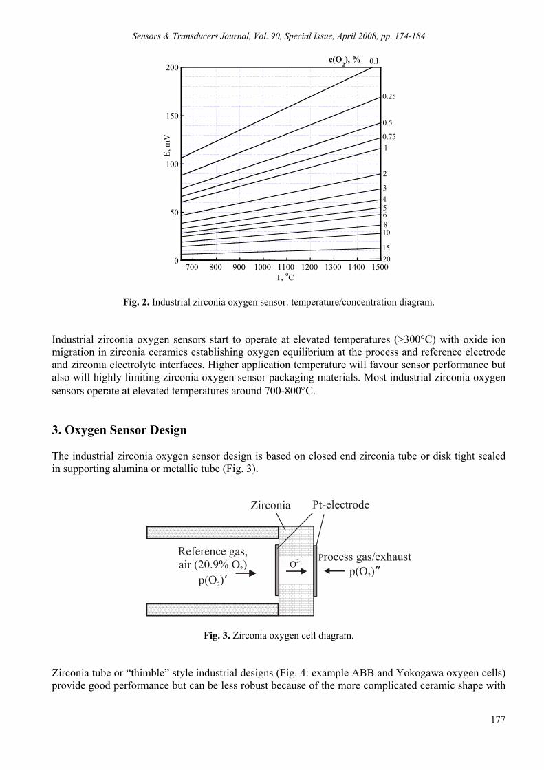
Sensors & Transducers Journal, Vol. 90, Special Issue, April 2008, pp. 174-184
177
0
50
100
150
200
700 800 900 1000 1100 1200 1300 1400 1500
E, m
V
T, oC
0.1
0.25
0.5
c(O2), %
1
2
3456810
1520
0.75
Fig. 2. Industrial zirconia oxygen sensor: temperature/concentration diagram.
Industrial zirconia oxygen sensors start to operate at elevated temperatures (>300°C) with oxide ion migration in zirconia ceramics establishing oxygen equilibrium at the process and reference electrode and zirconia electrolyte interfaces. Higher application temperature will favour sensor performance but also will highly limiting zirconia oxygen sensor packaging materials. Most industrial zirconia oxygen sensors operate at elevated temperatures around 700-800°C. 3. Oxygen Sensor Design The industrial zirconia oxygen sensor design is based on closed end zirconia tube or disk tight sealed in supporting alumina or metallic tube (Fig. 3).
O2-Reference gas,air (20.9% O )2
p(O )2 ’
Process gas/exhaustp(O )2 ”
Zirconia Pt-electrode
Fig. 3. Zirconia oxygen cell diagram. Zirconia tube or “thimble” style industrial designs (Fig. 4: example ABB and Yokogawa oxygen cells) provide good performance but can be less robust because of the more complicated ceramic shape with

Sensors & Transducers Journal, Vol. 90, Special Issue, April 2008, pp. 174-184
178
flange and thermal stresses across the tube. Thermal balance throughout the electrochemically active area of the zirconia cell is also not optimal.
ABB Yokogawa
Rosemount
Fig. 4. Design of industrial zirconia oxygen cells.
Disk-shape zirconia ceramics brazed into E-Brite supporting tube (Fig. 4, Rosemount) offer an advantage of much less temperature differential across the reference/process sides and reduced thermal stresses on the zirconia ceramics because of close match of thermal expansion coefficients. A special highly porous Pt-zirconia cermet electrode (Fig. 5) was developed to open TPB interface for the oxygen reaction and to improve oxygen sensor response and life time.
Fig. 5. SEM image of Pt-cermet process electrode. The most preferable application of the industrial oxygen sensor would be in-situ application close to the process to measure with the presence of extreme temperatures and hazardous chemicals. Industrial zirconia oxygen probes are designed to survive in such environment for years (Figs. 6-7).

Sensors & Transducers Journal, Vol. 90, Special Issue, April 2008, pp. 174-184
179
Fig. 6. ZR202G Oxygen Analyzer (Yokogawa).
Fig. 7. X-STREAM O2 Analyzer (Rosemount Analytical). Special protective shield, internal calibration line and reference gas line are made from special alloys like Inconel, Hastelloy or stainless steel SS 316L with excellent oxidation/corrosion resistance in severe high temperature process environment (Fig. 8).
Fig. 8. X-STREAM O2 probe sensor assembly.
A special oxygen cell with improved thermal balance and ceramic or metallic diffusers for the high particulate applications are common options to improve Oxygen Analyzer performance (Fig. 9).

Sensors & Transducers Journal, Vol. 90, Special Issue, April 2008, pp. 174-184
180
Oxygen cellImproved thermal
balance, cal gas deliveryCal gas line
Diffuser
Heater housing
Fig. 9. X-STREAM O2 cell assembly.
4. Combustion Process Monitoring and Control with Zirconia Oxygen Analyzers Industrial zirconia oxygen analyzers are used for combustion monitoring and control in a wide variety of applications ranging from energy-consuming industries, such as iron and steel, electric power, oil and petrochemical, ceramics, pulp and paper, food, and textiles, to various combustion facilities, e.g., boilers or incinerators. To have perfect combustion, CO2 should be maximized and O2 concentration should be close to zero in the flue gas stream (Fig. 10).
0.0
5.0
10
15
20
25
30
-12 -8 -4 0 4 8 12 16 20
Gas
con
cent
ratio
n (%
)
Oxygen concentration (%)
N2
balanced
CO2
CO
O2
% Deficiency % Excess
H2O
N2
Fig. 10. Combustion gas composition diagram.
In perfect combustion, the oxygen and fuel combine in an ideal ratio producing primarily carbon dioxide, CO2 and water, H2O with traces of other gases like sulfur dioxide, SO2 and nitrogen oxides, NOx coming from fuel impurities and nitrogen oxidation (from air). This stiochiometric point with the highest efficiency and the lowest emissions will be never achieved in the real combustion because of
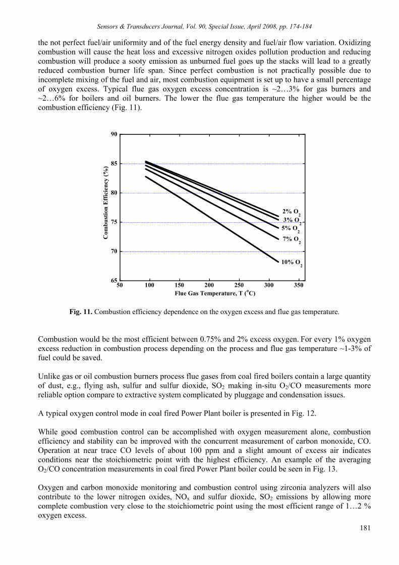
Sensors & Transducers Journal, Vol. 90, Special Issue, April 2008, pp. 174-184
181
the not perfect fuel/air uniformity and of the fuel energy density and fuel/air flow variation. Oxidizing combustion will cause the heat loss and excessive nitrogen oxides pollution production and reducing combustion will produce a sooty emission as unburned fuel goes up the stacks will lead to a greatly reduced combustion burner life span. Since perfect combustion is not practically possible due to incomplete mixing of the fuel and air, most combustion equipment is set up to have a small percentage of oxygen excess. Typical flue gas oxygen excess concentration is ~2…3% for gas burners and ~2…6% for boilers and oil burners. The lower the flue gas temperature the higher would be the combustion efficiency (Fig. 11).
65
70
75
80
85
90
50 100 150 200 250 300 350
Com
bust
ion
Eff
icie
ncy
(%)
Flue Gas Temperature, T (oC)
5% O2
3% O2
7% O2
10% O2
2% O2
Fig. 11. Combustion efficiency dependence on the oxygen excess and flue gas temperature.
Combustion would be the most efficient between 0.75% and 2% excess oxygen. For every 1% oxygen excess reduction in combustion process depending on the process and flue gas temperature ~1-3% of fuel could be saved. Unlike gas or oil combustion burners process flue gases from coal fired boilers contain a large quantity of dust, e.g., flying ash, sulfur and sulfur dioxide, SO2 making in-situ O2/CO measurements more reliable option compare to extractive system complicated by pluggage and condensation issues. A typical oxygen control mode in coal fired Power Plant boiler is presented in Fig. 12. While good combustion control can be accomplished with oxygen measurement alone, combustion efficiency and stability can be improved with the concurrent measurement of carbon monoxide, CO. Operation at near trace CO levels of about 100 ppm and a slight amount of excess air indicates conditions near the stoichiometric point with the highest efficiency. An example of the averaging O2/CO concentration measurements in coal fired Power Plant boiler could be seen in Fig. 13. Oxygen and carbon monoxide monitoring and combustion control using zirconia analyzers will also contribute to the lower nitrogen oxides, NOx and sulfur dioxide, SO2 emissions by allowing more complete combustion very close to the stoichiometric point using the most efficient range of 1…2 % oxygen excess.

Sensors & Transducers Journal, Vol. 90, Special Issue, April 2008, pp. 174-184
182
Fig. 12. Oxygen monitoring in the combustion process using X-STREAM O2 probe.
0
50
100
150
200
0.0
1.0
2.0
3.0
4.0
5.0
6.0
0 20 40 60 80 100 120 140 160
[CO
] (pp
m)
[O2]
(%)
t (days)
Coal fired Power Plant (3...4% O2, ~0.4 % SO2)X-STREAM O2/In-Situ CO-sensor
Fig. 13. O2/CO monitoring in combustion process.
Because of the combustion process temperature variation oxygen analyzer will also see significant temperature rising and dropping during the process monitoring and control. To provide oxygen sensor reliable accuracy and signal stability in the process changing environment (especially temperature) zirconia oxygen analyzer should be thermally balanced to eliminate effect of the thermal junction points contributing to the oxygen sensor signal (up to 10 mV for some oxygen analyzers on the market) and compromising oxygen measurements, e.g., 3±1 % O2. Process temperature variation will have very little effect on the slope and constant of the new Rosemount Analytical X-STREAM O2 Analyzer [10]. Error introduced by the process temperature variation between 25 and 600°C will be less than ±0.025 % O2 (Fig. 14). This new industrial Oxygen Analyzer will provide stable and accurate oxygen measurements in a wide oxygen concentration range
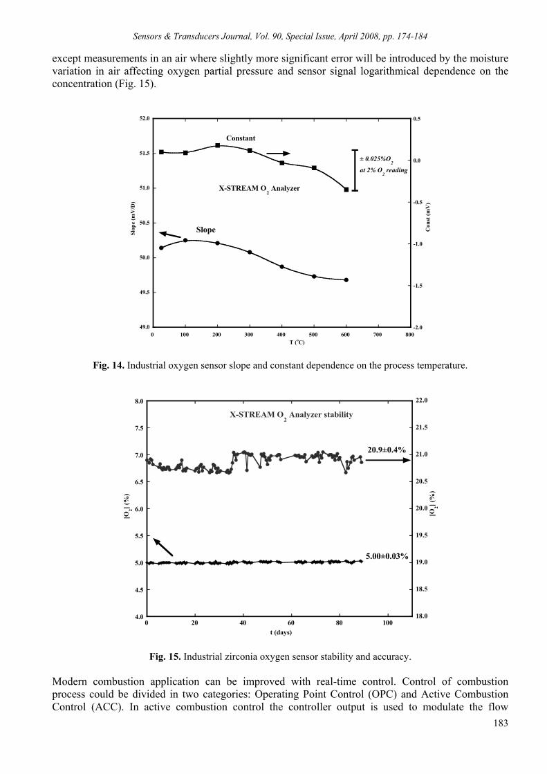
Sensors & Transducers Journal, Vol. 90, Special Issue, April 2008, pp. 174-184
183
except measurements in an air where slightly more significant error will be introduced by the moisture variation in air affecting oxygen partial pressure and sensor signal logarithmical dependence on the concentration (Fig. 15).
49.0
49.5
50.0
50.5
51.0
51.5
52.0
-2.0
-1.5
-1.0
-0.5
0.0
0.5
0 100 200 300 400 500 600 700 800
X-STREAM O2 Analyzer
Slop
e (m
V/D
)
Con
st (m
V)
T (oC)
Constant
Slope
± 0.025%O2
at 2% O2 reading
Fig. 14. Industrial oxygen sensor slope and constant dependence on the process temperature.
4.0
4.5
5.0
5.5
6.0
6.5
7.0
7.5
8.0
18.0
18.5
19.0
19.5
20.0
20.5
21.0
21.5
22.0
0 20 40 60 80 100
X-STREAM O2 Analyzer stability
[O2] (
%)
[O2] (
%)
t (days)
5.00±0.03%
20.9±0.4%
Fig. 15. Industrial zirconia oxygen sensor stability and accuracy. Modern combustion application can be improved with real-time control. Control of combustion process could be divided in two categories: Operating Point Control (OPC) and Active Combustion Control (ACC). In active combustion control the controller output is used to modulate the flow

Sensors & Transducers Journal, Vol. 90, Special Issue, April 2008, pp. 174-184
184
properties, e.g., fuel flow rate modulation. ACC has been achieved in many cases with variable degree of success in laminar flame burners and turbulent combustors. Lean premixed combustion is one of the effective approaches reducing NOx emissions because of the lower flame temperature. Unfortunately, this approach has two major drawbacks: blowout and instability control [2]. To meet the requirements of the active combustion control strategy, the sensor system must be able to determine the states of the combustion system rapidly and accurately. Combustion instabilities usually occur with frequencies less than 500 Hz, a kHz real-time sensor response is required to provide an effective feedback control signal. In operating point control (OPC) the fuel injection is regulated in order to maintain certain flame parameters. Unfortunately the air quantity flowing in the combustor is not known with sufficient accuracy and OPC was based on limited information of actual flame properties and estimated air mass flux. A precise adjustment of the fuel/air ratio is based on oxygen concentration measurements in flue gas using zirconia oxygen sensor signal. More details on zirconia oxygen sensor materials, sensor performance and sensor application limits in different environment can be found in reviews and just published book [11-15]. References [1]. M. Kleitz, E. Siebert, P. Fabry, J. Fouletier, Solid state electrochemical sensors, in Sensors a
comprehensive survey, Eds. W. Göpel, J. Hesse, J. N. Zemel, VCH, New York, Vol. 2, 1991, pp. 341-428. [2]. N. Docquier, S. Candel, Process control and sensors: a review, Progress in Energy and Combustion
Science, Vol. 28, 2002, pp. 107-150. [3]. H. Peters, H. -H. Möbius, Procedure for the gas analysis at elevated temperatures using galvanic solid
electrolyte elements. DD-Patent 21673, 1961. [4]. J. Weissbart, R. Ruka, Oxygen gauge, Rev. Sci. Instrum. ,Vol. 32, 1961, pp. 593-595. [5]. W. A. Fisher, D. Janke, Metallurgische Elektrochemie, Springer Verlag, New York, 1977. [6]. G Velasco and J -P Schnell, Gas sensors and their applications in the automotive industry, J. Phys. E: Sci.
Instrum., Vol. 16, 1983, pp. 973-977. [7]. J. Riegel, H. Neumann, H. -M. Wiedenmann, Exhaust gas sensors for automotive emission control, Solid
State Ionics, Vol. 152-153, 2002, pp. 783-800. [8]. J.-H. Lee, Review on zirconia air-fuel ratio sensors for automotive applications, J. Mater. Sci., Vol. 38,
2003, pp. 4247-4257. [9]. H. Neumannn, G. Hoetzel and G. Lindermann, Advanced planar oxygen sensors for future emission control
strategies, SAE Technical Paper, 970459, 1997, pp. 1-9. [10]. Rosemount Analytical Inc. Web (http://www. emersonprocess. com/raihome/gas/). [11]. W. C. Maskell, B. C. H. Steele, Solid state potentiometric oxygen gas sensors, J. Appl. Electrochemistry,
Vol. 16, 1984, pp. 475-489. [12]. J. Fouletier, Gas analysis with potentiometric sensors: a review, Sensors and Actuators, Vol. 3, 1982/83,
pp. 295-314. [13]. H.-H. Möbius, Solid state electrochemical potentiometric sensors for gas analysis, in Sensors a
comprehensive survey, Eds. W. Göpel, J. Hesse, J. N. Zemel, VCH, New York, Vol. 3, 1992, pp. 1105-1154.
[14]. S. Zhuiykov, Electrochemistry of zirconia gas sensors, CRC Press, Boca Raton/London/New York, 2008, pp. 1-297.
[15]. P. Shuk, U. Guth and E. Bailey, Industrial zirconia oxygen sensor: state of art, ICST-2007, 2007, pp. 488-492.
___________________
2008 Copyright ©, International Frequency Sensor Association (IFSA). All rights reserved. (http://www.sensorsportal.com)

Sensors & Transducers Journal, Vol. 90, Special Issue, April 2008, pp. 185-194
185
SSSeeennnsssooorrrsss &&& TTTrrraaannnsssddduuuccceeerrrsss
ISSN 1726-5479© 2008 by IFSA
http://www.sensorsportal.com
Measurement of Digital Camera Image Noise for Imaging Applications
1Kenji IRIE, 2Alan E. McKINNON, 2Keith UNSWORTH, 1Ian M. WOODHEAD
1Lincoln Ventures Ltd, P.O. Box 133, Lincoln, Christchurch 7640, New Zealand Tel.: ++64-3-325-3712, fax ++64-3-325-3712,
2 Applied Computing Group, Lincoln University, Canterbury, New Zealand E-mail: iriek, [email protected], mckinnon, [email protected]
Received: 15 October 2007 /Accepted: 20 February 2008 /Published: 15 April 2008 Abstract: Noise within captured images from digital cameras is unavoidable and can confound or reduce the performance of an image-based application. It is present in the captured photons, generated in the sensor electronics, and an inherent part of the digital signal processing. A measure of image noise can allow an algorithm to fine tune its parameters to minimize the effects of noise, or could be used in a filter to remove noise prior to image analysis. This paper presents an overview of image noise and describes a method for measuring noise quantity for use in image-based applications. Copyright © 2008 IFSA. Keywords: Image analysis, Noise measurement, CCD image sensor, CMOS image sensor 1. Introduction Advances in digital image sensors have led to their ubiquitous use in many industrial and consumer applications. Industrial applications often attempt to extract useful information from the digital images, which is limited in robustness and performance because of image noise. The sources of image noise are well documented [1-3], with the number of sources increasing with camera complexity [4, 5]. The analysis of modelled image noise becomes more difficult with increasing camera complexity, so we present a method of noise analysis that does not require a model and is dependent only upon output images from a camera. A background on image noise is provided, followed by the method used for measuring noise to characterize a camera’s effective noise output, suitable for an image or video based application.

Sensors & Transducers Journal, Vol. 90, Special Issue, April 2008, pp. 185-194
186
2. Sources of Camera and Image Noise A summary of sources of camera and image noise is provided. Existing terminology used for sources of image sensor noise varies and is inconsistent, depending upon the author and the approach taken for its analysis. Multiple definitions will be provided in the text where appropriate. 2.1. Offset Fixed-Pattern Noise Offset fixed-pattern noise (FPN) arises from variations due to device mismatches during sensor fabrication and their associated dark currents. Dark currents are leakages produced by surface generation and minority carriers thermally generated in the sensor well, and in variations between transistors in active-pixel elements. The expected value for a pixel’s dark current is constant for a given operating condition though it increases with exposure time. FPN is the total pixel-to-pixel variation occurring in an image sensor, and is alternatively referred to as Dark Signal Non-Uniformity or DSNU [1, 3, 6-8]. FPN is temperature dependent and is measurable in dark conditions. 2.2. Photo Response Non-Uniformity The pixel output to a given illumination is dependent on the variations in geometry, substrate material, microlenses, and any transistors that may be present around the pixel. The variations are nearly impossible to eliminate and the resulting effect is described as Photo Response Non-Uniformity (PRNU). It is dependent upon illumination and is prominent under high illumination levels [3]. It is also referred to as gain fixed-pattern noise. 2.3. Shot Noise Shot noise is a Poisson process that arises from random fluctuations in sampling when discrete quanta are measured. Significant shot noise sources in an image sensor are in the capturing of photons in the photon-detection stage, in the temporal variation of dark currents, and in transistor semiconductors. Sources of shot noise generated by independently moving charges, such as in current movement in metallic conductors, exhibit long-range correlations [9] and are considered as minor contributors to the total shot noise present in an image sensor. The number of dark-current shot noise electrons doubles with every 8º C rise in temperature [1, 10], and is proportional to the pixel integration time. Photon shot noise is dependent upon the mean number of captured photons, and therefore increases with sensor irradiance. 2.4. Readout Noise Readout noise describes the total temporal noise added during the process of reading a signal out of an image sensor, from the photoreceptor through to the analogue-to-digital conversion process. It includes pixel reset noise, thermal noise sources (Johnson-Nyquist), 1/f (flicker) noise sources, and other minor contributors such as conductor shot noise. The resetting of the charge sense capacitor to a reference voltage level introduces noise from thermal fluctuations, often described as ‘kT/C’ or reset noise. A common method used to reduce the capacitor-reset variations is correlated double sampling (CDS) [1, 11]. CDS samples the noise value on the sense capacitor after reset, and subtracts it from the sample of pixel data after charge transfer. There are

Sensors & Transducers Journal, Vol. 90, Special Issue, April 2008, pp. 185-194
187
more complex implementations of CDS used [12], however the details of these are beyond the scope of this paper. Any electrical conductor exhibits equilibrium fluctuations due to the random thermal motion of the charge carriers. This thermal, or Johnson-Nyquist noise, occurs regardless of the voltage applied to the conductor [9, 13]. 1/f or ‘flicker’ noise is generated in the photo-diodes and in the low-bandwidth analogue operation of MOS transistors due to imperfect contacts between two materials [1, 13]. It is pink-coloured, and the level of noise is dependent upon the frequency of the pixel sampling rate. 2.5. Column Noise Many CMOS image sensors use column amplifiers to enable high pixel data rates [1]. Variations between transistor amplifiers result in both offset and gain variations between columns of an image, increasing spatial variation along the rows of an image. 2.6. Demosaicing Many single-sensor color cameras use color filter arrays (CFAs) to restrict the pixel bandwidths to a particular range in the optical spectrum. A commonly used CFA is the Bayer matrix that reduces each pixel’s bandwidth to approximately 1/3 of the visible wavelengths of light. A method of colour interpolation called demosaicing is then employed to generate full-colour values at each pixel in an image [14]. The demosaicing process used to interpolate the color data for each pixel is generally manufacturer dependent and unknown. 2.7. Quantization Digital images are often quantized to 8-16 bits per color channel for export from the camera. Where the quantization step is very small compared to variations within the image, the quantization process adds noise to the image according to the following equation [15]:
(1)
where q is the quantizing step. For q=1 σquantization = 0.29. 2.8. Other Considerations Many digital cameras apply a series of digital filters such as edge enhancement, color balancing, gain, and gamma correction that all affect the noise characteristics of the image1. Lossy image compression is often applied that reduces both color and edge acuity. CCDs are also prone to smearing and blooming due to the limited charge capacity of the photodiodes. This may cause some correlation of data along columns of pixels. In this work the digital camera filters have been disabled or set to neutral and images have been
1 The common brightness or black level adjustment simply alters the DC offset of the image and does not affect its noise detail.

Sensors & Transducers Journal, Vol. 90, Special Issue, April 2008, pp. 185-194
188
transferred in the RGB format2. 3. Measurement of Image Noise The sources of noise described in Section 2 can be segmented into three general categories for the purpose of noise measurement: spatial noise, temporal noise, and total image noise. Spatial noise has a dependency upon orientation of the analysis due to column noise. Measurement of spatial noise is calculated along the rows of an image to ensure that any column noise is included in the noise analysis. 3.1. Spatial Noise Spatial noise is exhibited as variations between the pixels in an image given a constant illumination across the sensor, and is dominated by offset FPN at low illuminations and by PRNU at high illuminations [16]. Knowledge of spatial noise is useful in applications where images are averaged prior to analysis (e.g., low-light applications like astronomy where multiple images may be captured to increase effective exposure time). Images of spatial noise can be achieved by averaging a series of images containing smooth areas of constant reflectance, removing the temporal variations. The
generation of an image of spatial noise, ( , )image i j , is given by:
1
( , )( , )
n
kkP i j
image i jn
==∑
, (2)
where n is the number of images. ( , )kP i j is the pixel value for row i, column j in the kth image. A
second-order polynomial can be fitted to each row of ( , )image i j to describe any optical effects such as shadowing or vignetting. The residuals after subtraction of the polynomial-fitted data can be concatenated for each row and the unbiased standard deviation σ calculated, giving the value of the
spatial noise spatialσ . 3.2. Temporal Noise Temporal noise varies between images and is dependent on illumination. Knowledge of temporal noise is useful in applications where images are compared or subtracted before analysis (e.g., in a subtraction-based motion detection algorithm). Temporal noise can be measured by taking the average value of the variations exhibited by a pixel over a series of images. The equation for temporal noise
tempσ for a given sensor irradiance is therefore:
1 1
( , )
temp
j i
y x
x y
i j
σ
σ = ==×
∑∑,
(3)
2 Although transferred to the computer in RGB format, the camera may not necessarily operate internally in the RGB space.

Sensors & Transducers Journal, Vol. 90, Special Issue, April 2008, pp. 185-194
189
where i and j are the number of rows and columns respectively and ( , )x yσ is the unbiased standard deviation of the pixel value at (x, y) over n images. 3.3. Total Noise The total noise in an image is the combined effect of all spatial and temporal noises present in an image. It is useful in applications where a single image is used for processing (e.g., in an edge detection algorithm). To measure total image noise, the process of fitting a second-order polynomial to each of the n images is applied in the same fashion as the calculation of spatial image noise spatialσ in
( , )image i j . A series of unbiased standard deviations for each row of the kth image of the n image set is
calculated, giving kσ . The average of kσ over all n images gives totalσ . 4. Experiment The measurement of image noise requires a series of static images containing areas of constant detail. The Gretag Macbeth Color Checker (GMB chart) provides a useful series of colour patches suitable for noise measurement. The lower portion of the chart consists of grey-scale panels that provide a range of reflectances (3.1 to 90.0 CIE Y values) that can be used for analysis of both colour and monochromatic cameras. The cameras were defocused to reduce the effect of high-frequency content in the observed panels that could affect the noise analysis. The illumination sources (combined fluorescent and incandescent3) were positioned above the camera and directed towards the chart such that the image was free from direct specular reflection. A single set of images for each camera was used for noise measurement analysis. Standard statistical methods can determine an appropriate number of samples (either pixels or images) required to achieve a desired confidence interval and error for the observed sample mean [17]. For a population with an unknown mean µ and unknown standard deviation σ, a confidence interval for the population mean, based on a random sample of size n, is: s
X tn
± × , (4)
where X is the mean of the sample population, s is the estimated standard deviation derived from the sample population, and t is the (1-C)/2 critical value for the t-distribution with n-1 degrees of freedom where C is the desired confidence interval. A standard confidence interval of 95% is used for this research. It was observed that s is rarely greater than five in most digital video images (with cameras in ‘auto’ mode, data values 0-255) in canonical lighting conditions. A suitable maximum level of error is one quantization step in the digital data, which is a value of one. From expression (4) above, this yields the following upper bound for the mean error:
3 Each light source was adjusted to provide similar camera RGB response for a grey-scale image.
Sensors & Transducers Journal, Vol. 90, Special Issue, April 2008, pp. 185-194
190
51 t
n≥ × (5)
The t-distribution is a function of n and C. Using standard t-distribution tables and choosing n=100 give a value of 1.962. Substituting these values into the right hand side of (5) gives a value of 0.981 and inequality (5) is satisfied. Note that this holds only for estimated standard deviations less than or equal to 5. Therefore an appropriate sample size to achieve a 95% confidence interval for noise measurement is 100 samples. Experiments were conducted at an ambient temperature of approximately 22° C. All digital camera effects such as colour balance and gamma were disabled in the experiments, although the method for noise measurement described in Section 3 is suitable for any fixed camera settings. 4.1. CMOS Camera Noise Fig. 1 illustrates the spatial, temporal, and total noise measurement for the CMOS camera (Table 1) as described in Section 3, with each of the three colour channels showing similar noise responses.
0 50 100 150 200 2500
0.5
1
1.5
σsp
atia
l
µGMB panel
RedGreenBlue
0 50 100 150 200 250
0
0.5
1
1.5
σ tem
p
µGMB panel
RedGreenBlue
(a)
(b)
0 50 100 150 200 2500
0.5
1
1.5
σ tot
al
µGMB panel
RedGreenBlue
(c)
Fig. 1. CMOS camera noise: spatial (a), temporal (b), total (c).

Sensors & Transducers Journal, Vol. 90, Special Issue, April 2008, pp. 185-194
191
Table 1. UEYE UI1210-C camera details.
Parameter Value Sensor type ½″ CMOS (Bayer array) Native resolution 640 x 480 Video mode 24-bit RGB (8-bits/channel) Interface USB 2.0
4.5. CCD Camera Noise Fig. 2 illustrates the spatial, temporal, and total noise measurements for the CCD camera (Table 2). Experiments found that the green channel of the CCD camera was limited to values below approximately 150 when all digital effects were disabled. The cause of this effect is unknown and the illumination was set to ensure the green channel measurements for all channels were below 150.
0 50 100 1500
0.5
1
1.5
2
2.5
3
σ spa
tial
µGMB panel
RedGreenBlue
0 50 100 150
0
0.5
1
1.5
2
2.5
3σ t
emp
µGMB panel
RedGreenBlue
(a)
(b)
0 50 100 1500
0.5
1
1.5
2
2.5
3
σ tot
al
µGMB panel
RedGreenBlue
(c)
Fig. 2. CCD camera noise: spatial (a), temporal (b), total (c).

Sensors & Transducers Journal, Vol. 90, Special Issue, April 2008, pp. 185-194
192
Table 2. Unibrain Fire i400 camera details.
Parameter Value Sensor type Sony Wfine ICX098BQ ¼″ color
CCD (Bayer colour filter) Native resolution 640 x 480 Video mode 24-bit RGB (8-bits/channel) Interface IEEE-1394a (Firewire)
4.3. Temperature Offset FPN, dark current shot noise, readout noise, and column noise all depend upon temperature. The effect of temperature was analyzed for the CMOS and CCD cameras by capturing image sets at various temperatures with zero illumination. The cameras were placed inside a thermally insulated enclosure with a controllable heat source, and the ambient temperature and surface sensor temperatures were allowed to stabilize for approximately 10 minutes before images were captured. The temperatures were measured using thermocouples, with the sensor thermocouple mounted on the front of the integrated circuit package of each camera. Measurements of spatial and temporal noise were made, with results shown in Figs. 3 and 4. The graphs show almost opposite responses between the CCD and CMOS cameras with CCD temporal noise significantly greater than spatial noise and vice versa for the CMOS camera. The cause of the dip in the temperature noise curves for the CCD camera is unknown, but the same effect was evident in three separate experiments.
25 30 35 40 45 50 55 600
0.5
1
1.5
2
2.5
3
3.5
4
4.5
CMOS surface temperature (oC)
σ spa
tial(d
ark)
RedGreenBlue
25 30 35 40 45 50 55 60
0.5
0.55
0.6
0.65
0.7
CMOS surface temperature (oC)
σ tem
p(dar
k)
RedGreenBlue
(a)
(b)
Fig. 3. Spatial (a) and temporal (b) noise for varying CMOS surface temperature in dark conditions.
5. Discussion Figs. 1 and 2 highlight significant differences in the relative and total magnitudes of the cameras’ noise components. The spatial noise in the CMOS camera demonstrates a relatively large amount of offset FPN compared to the CCD, while the CCD camera demonstrates substantial amounts of PRNU as shown by the linearly increasing spatial noise. The channel responses of the CMOS camera exhibit similar noise magnitudes in all forms of noise, yet the CCD demonstrates higher noise in its red and blue channels. Apart from green values below approximately 50, the CMOS camera exhibits lower noise than the CCD camera in temporal and total noise value when operating in an ambient environment of approximately 22° C.

Sensors & Transducers Journal, Vol. 90, Special Issue, April 2008, pp. 185-194
193
30 35 40 45 500
0.05
0.1
0.15
0.2
0.25
CCD surface temperature (oC)
σ spa
tial(d
ark)
RedGreenBlue
30 35 40 45 50
0
0.5
1
1.5
2
CCD surface temperature (oC)
σ tem
p(dar
k)
RedGreenBlue
(a)
(b)
Fig. 4. Spatial (a) and temporal (b) noise for varying CCD surface temperature in dark conditions. Experiments have shown that temperature can have a significant impact on image noise. The CMOS temperature response fits with the theory that camera noise increases with temperature, whereas the CCD response demonstrates an uncharacteristic response by showing a reduction on noise between 30° C and 40° C. It is clearly important to ensure that any noise analysis for the purpose of an image-processing application occurs at the environmental temperature that the camera will be operating in. The results of this work have shown considerable differences in noise characteristics between the CCD and CMOS cameras analyzed. The quantity and quality of noise cannot be assumed to be consistent between cameras, and should be measured prior to any application incorporating noise values as parameters. 6. Conclusion A method for measuring noise in cameras has been developed that can be used as an input into image processing applications. 100 images of a patch chart such as the GMB chart can provide the necessary information to measure the amount of spatial, temporal and total noise in a camera. The amount and shape of the noise response to illumination can vary significantly from camera to camera, and can have a high dependency upon the environmental temperature. Acknowledgement This work was supported by the New Zealand Foundation for Research, Science and Technology programme LVLX0401. References [1]. J. Nakamura, Image Sensors and Signal Processing for Digital Still Cameras, CRC Press, 2006. [2]. R. E. Flory, Image acquisition technology, In Proceedings of the IEEE, Vol. 73, 1985, pp. 613-637. [3]. A. El Gamal and H. Eltoukhy, CMOS image sensors, Circuits and Devices Magazine, IEEE, Vol. 21, 2005,
pp. 6-20.

Sensors & Transducers Journal, Vol. 90, Special Issue, April 2008, pp. 185-194
194
[4]. L. Brouk and Y. Nemirovsky, CMOS SOI image sensor, In Proceedings of the IEEE International Conference on Electronics, Circuits and Systems, Vol. 11, 2004, pp. 156-159.
[5]. T. Anaxagoras, N. Guerrini, R. Turchetta, and N. M. Allinson, High Dynamic Range Sensor Active Pixel Sensor, In Proceedings of the First International Conference on Sensing Technology, 21-23 November 2005, pp. 448-453.
[6]. R. Costantini and S. Süsstrunk, Virtual Sensor Design, In Proceedings of SPIE Sensors and Camera Systems for Scientific, Industrial, and Digital Photography Applications V., 2004, Vol. 5301, pp. 408-419.
[7]. T. Chen, P. B. Catrysse, A. El Gamal, and B. A. Wandell, How small should pixel size be?, In Proceedings of SPIE Sensors and Camera Systems for Scientific, Industrial, and Digital Photography Applications, Vol. 3965, 2000, pp. 451-459.
[8]. P. B. Catrysse, M. Wang, and A. El Gamal, Comparative analysis of color architectures for image sensors, In Proceedings of SPIE Sensors, Cameras, and Applications for Digital Photography, Vol. 3650, March 1999, pp. 26-35.
[9]. P. Horowitz and W. Hill, The Art of Electronics, Second ed. Melbourne, 1989. [10]. G. E. Healey and R. Kondepudy, Radiometric CCD camera calibration and noise estimation, IEEE Trans.
on Pattern Analysis and Machine Intelligence, Vol. 16, 1994., pp. 267-276 [11]. CCD Technology Primer, Dalsa Inc (www.dalsa.com). [12]. S. Baier, CCD Imaging Systems, Burr-Brown Corp. [13]. H. W. Ott, Noise Reduction Techniques in Electronic Systems, Second ed. Canada, 1988. [14]. B. K. Gunturk, J. Glotzbach, Y. Altunbasak, R. W. Schafer, and R. M. Mersereau, Demosaicking: Color
Filter Array Interpolation (Exploring the imaging process and the correlations among three color planes in single-chip digital cameras), IEEE Signal Processing, Vol. 22, 2005, pp. 44-54.
[15]. H. Baher, Analog and digital signal processing, John Wiley & Sons Ltd, 1990. [16]. K. Irie, A. E. McKinnon, K. Unsworth, and I. M. Woodhead, A comparison of noise in CCD and CMOS
image sensors, In Proc. Image and Vision Computing New Zealand Great Barrier Island, New Zealand, 2006, pp. 43-48.
[17]. G. K. Bhattacharyya and R. A. Johnson, Statistical concepts and methods, John Wiley & Sons, Inc., 1977.
___________________ 2008 Copyright ©, International Frequency Sensor Association (IFSA). All rights reserved. (http://www.sensorsportal.com)

Sensors & Transducers Journal, Vol. 90, Special Issue, April 2008, pp. 195-208
195
SSSeeennnsssooorrrsss &&& TTTrrraaannnsssddduuuccceeerrrsss
ISSN 1726-5479© 2008 by IFSA
http://www.sensorsportal.com
Calibration-free Image Sensor Modelling Using Mechanistic Deconvolution
Shen Hin Lim, Tomonari Furukawa
University of New South Wales, Sydney, Australia E-mail: [email protected]
Received: 15 October 2007 /Accepted: 20 February 2008 /Published: 15 April 2008 Abstract: This paper presents a calibration-free approach to modelling image sensors using mechanistic deconvolution, whereby the model is derived using mechanical and electrical properties of the sensor. In this approach, effective focal length is determined using thick lens properties approximated from lens system. The accumulated uncertainties and constraints from sensor properties are utilized with approximated aperture stop position offset to estimate distortion effects, and, eventually to derive corrected image data. This reduces dependency on image data, and, as a result, does not require experimental setup or calibration. An experiment was constructed to evaluate accuracy of model created by the approach, and its robustness to changes in sensor properties without recalibration. The model was compared with a pre-calibrated model using two sensors with different specifications. The model achieved similar accuracy with one-fifth of number of iterations. The approach was also shown to be robust and, in comparison to pre-calibrated model, improved the accuracy significantly. Copyright © 2008 IFSA. Keywords: Image sensor, Sensor modelling, Mechanistic deconvolution, Lens distortion, Calibration 1. Introduction As off-the-shelf image sensors are not perfect, information obtained from them cannot be perfectly accurate. Consequently, corrective sensor modelling, also known as calibration, is an important process for applications that require accurate geometric measurements [1]. In addition, the process needs to be computationally inexpensive for real-time applications. The process has long been an important issue in photogrammetry and computer vision fields, and more recently, in the area of robotics and automation, for example, mobile robot navigation [2].

Sensors & Transducers Journal, Vol. 90, Special Issue, April 2008, pp. 195-208
196
Conventionally, sensors have been corrected by either iteratively applying non-linear optimization, or analytically deriving a closed-form solution. The former technique utilizes the initial guess of sensor parameters, to derive a non-linear solution iteratively and attains accurate calibration [3, 4]. This technique, however, requires good estimation of the initial guess for accurate calibration and is computationally expensive. On the contrary, the computationally inexpensive closed-form solution is derived by a set of linear equations, which do not take distortion into account and yield inaccurate results [3, 5]. The disadvantages in these classical techniques have motivated the researchers to develop new techniques, which may be categorized into two groups: the two-step method [3, 5-9], and self-calibration [10-12]. The two-step method was proposed by Tsai [3]. A closed-form solution is initially derived using radial alignment constraints to estimate extrinsic parameters and effective focal length. The parameters are then used to derive a non-linear solution iteratively and retrieve radial distortion parameter and corrected effective focal length. This technique reduces the number of required iterations considerably. Weng et al. [5] improved the two-step method and successfully estimated tangential distortion parameters. A number of other groups have also proposed techniques that derive radial distortion parameters analytically, prior to finding a non-linear solution iteratively, in an attempt to reduce the number of iterations [6, 7]. Similarly, Bailey [8] derived an analytical solution to estimate the parameters using parabolic curves. For real-time applications, Park and Hong [9] simplified Tsai’s technique by applying look-up-table (LUT) techniques. Maybank et al. [10] developed a different type of calibration technique, namely self-calibration. In contrast to the two-step method, this technique does not require a calibration setup that includes a calibration object with known 3D geometrical features. The intrinsic parameters are assumed to be constant to reduce computational expenses. In comparison to other technique, this method requires at least three different orientations and achieves lower accuracy, despite having higher flexibility. The self-calibration technique has been modified and extended to include different constraints, mainly camera motion and scene constraints, to increase its accuracy [11]. Zhang [12] has fused this technique with the two-step method and was able to reduce number of orientations whilst having better robustness, as compared to the self-calibration. These techniques have a common approach; the image sensor is evaluated with a known image. These models have shown to reproduce parameters of image sensor successfully, negating the need to manually obtain the sensor’s mechanical and electrical properties. Nevertheless, the sensor model derived from these properties may also derive image sensor parameters and reduce the dependency of the image quality, and, acts as an alternative solution to calibration. This paper presents a calibration-free approach to modelling image sensors using mechanistic deconvolution. The proposed approach evaluates the image sensor using its mechanical and electrical properties. A thick lens, which determines the effective focal length, is used to approximate the sensor lens system. In contrast to conventional models, distortion model is developed using uncertainties and constraints present in the sensor. The approach also uses aperture stop position offset to further evaluate lens distortion effect. In this approach, three assumptions are made: firstly, a distance between sensor and its plane of view is known; secondly, image plane is orthogonal to its z-axis; thirdly, only radial distortion is considered. One advantage of this approach is the removing requirement of experimental evaluation of image sensors, while remaining robust to changes in its properties. The paper is organized as follows. Section 2 reviews the general formulation of existing problem and techniques. The model derived from the proposed approach, namely mechanistic deconvolutive model is presented in Section 3. This is followed by numerical examples in Section 4, including experimental setup and procedure. Finally, Section 5 presents the conclusion of this paper.

Sensors & Transducers Journal, Vol. 90, Special Issue, April 2008, pp. 195-208
197
2. Conventional Sensor Models 2.1. Pinhole Camera Model The transformation from object world coordinate system to image plane is shown in this sub-section, and, its formulations are based on pinhole camera model; that is the ideal form of image sensor model. Initially, the position of an object with respect to the world coordinate system, xw=[xw, yw, zw]T, is transformed to that with respect to the camera 3D coordinate system, xp=[xp, yp, zp]T, as p wx Rx t= + , (1) where R is the rotational matrix and t is the translational vector. The R and t are known as the extrinsic parameters. The position xp is then converted to the image plane coordinate system, xu=[u, v, 1]T, using its z-component and intrinsic parameters in A: u px Ax= (2) Here A, formulated on the assumption that the image plane axes are parallel to the world coordinate system, is given by
0
0
00 with0 0 1
x xx
y
yy
ff u f pf v
ff p
A
⎧ ⎫⎡ ⎤ =⎪ ⎪⎢ ⎥= ⎨ ⎬⎢ ⎥⎪ ⎪=⎢ ⎥⎣ ⎦ ⎩ ⎭
, (3)
where f is the effective focal length, [u0, v0] is the principal point coordinates and ps=[px, py]T is the pixel size. 2.2. Distortion Model The previous sub-section considers the ideal form of sensor model, and unable to include the distortion effects inherent in image sensors. These effects, namely radial and tangential distortions, produce the distorted coordinates, xd=[ud, vd]T. Hence, by using xd, the corrected image data coordinates, also known as undistorted coordinates xu are ( )2
1
1 1iu i d dK rx x g⎛ ⎞= + − +⎜ ⎟
⎝ ⎠∑ , (4)
where K1:i are radial distortion factors, and g and rd are as follows ( )
( )
2 21 2
2 22 1
2 2
2 2
d d d d
d d d d
P r u P u v
P r v Pu vg
⎡ ⎤+ +⎢ ⎥=⎢ ⎥+ +⎣ ⎦
(5)
2 2
d d dr u v= + , (6) where P1 and P2 are tangential distortion factors. It is noted that image data are highly affected by radial distortion.

Sensors & Transducers Journal, Vol. 90, Special Issue, April 2008, pp. 195-208
198
2.3. Conventional Model Approach The previous sub-sections have shown that quality of image data is a dominant factor for modelling a given sensor. Fig. 1 illustrates the general approach of conventional models. The image data sI is initially utilized to estimate initial extrinsic and intrinsic parameters A, R and t, by deriving a closed-form solution using (1)–(3). The initial parameters are then used with other inputs, which are target geometric features and radial alignment constraint, to determine initial distortion factors K1 and K2 as defined in (4). The derived A, R, t, K1 and K2 are inserted into the non-linear optimization process with given sI such that these parameters satisfy (1)–(6). The parameters obtained from non-linear optimization process derive undistorted coordinates xu, and, obtain the corrected image eventually.
Fig. 1. Conventional technique. 3. Mechanistic Deconvolutive Model 3.1. Determining Effective Focal Length Using Optical Parameters In contrast to the conventional models, the proposed approach determines the effective focal length of the sensor by its lens system. Initially, the complex lens system is approximated by a thick lens system, to reduce required parameters and complexity. The thick lens system is defined as follows [13],
( ) ( )1 2 1 2
11 1 11t n
nf r r nr r
⎡ ⎤−= − − +⎢ ⎥
⎣ ⎦ , (7)
where n is the refractive index, r1 and r2 are the radii of curvature closest and farthest from the light source, and t is the overall lens thickness. By rearranging equation (7), the effective focal length f becomes
( ) ( )( )1 2
2 1 11 1nr rf
n nr n r t n=
− − + − (8)

Sensors & Transducers Journal, Vol. 90, Special Issue, April 2008, pp. 195-208
199
This equation shows that three components provide uncertainties in f; r1, r2 and t, which can be well approximated as Gaussian noise. This produces the modified effective focal length fd, as follows f
df f w= + , (9) where wf is the combination of uncertainties from r1, r2 and t. 3.2. Deriving Undistorted Coordinates Using Constraints, Uncertainties and Aperture Stop Position 3.2.1. Constraints and Uncertainties A general image sensor is constrained by three elements that are the pixel size, sensor chip, and diameter aperture. The pixel size, ps controls the possible smallest size of scene feature. This is defined as the feature resolution constraint, with its parameter (b1−b2)min. It is also constrained by fd and the distance between the scene feature and sensor, l as ( )1 2 min
0sd
lf
b b p− − ≥ , (10)
where b1=[xb1, yb1]T and b2=[xb2, yb2]T are the reference points that define the size vector of scene feature. The sensor chip acts as a field stop, and hence its size, sa=[sx, sy]T controls the size of the largest scene feature. Using ps and the pixel resolution pr=[pr
x, pry]T, sa is
a r ss p p= ⋅ (11) The field of view constraint is derived in the following manner, ( ) ( )1 2 max
2 tan 20; :i d
id
lsi x y
sb b e
θ− − ⋅ ≥ = , (12)
where (b1−b2)max is the field of view constraint parameter, θd is the field of view angle, and sd=(sx
2+sy2)0.5. The angle θd can also be derived as follows,
( )12 tan 2d d ds fθ −= (13) Equation (13) is rearranged and becomes ( )tan 2
2d
dd
sf
θ = (14)
and is substituted into equation (12), to obtain ( )1 2 max
0ad
lf
s b b− − ≥ (15)
and shows that fd and sa are the factors that affect the field of view constraint. Lastly, the final

Sensors & Transducers Journal, Vol. 90, Special Issue, April 2008, pp. 195-208
200
constraint, also known as the depth of field constraint, is affected by the diameter aperture size. In normal cases, the diameter aperture size da is used as the aperture stop to limit the number of rays, and resultantly affects the image brightness, Ib. The relationship between Ib, da and fd is 2
ab
d
dI f⎛ ⎞∝ ⎜ ⎟⎝ ⎠
(16)
The aperture stop also changes the exposure time te, as follows 2
12
fe
b
nt I⎛ ⎞∝ = ⎜ ⎟⎝ ⎠
, (17)
where nf is the f-number, a different representation of te. By introducing a linear constant q, (16) and (17) can be combined and nf is formulated as 2 d
fa
fnq d⎛ ⎞
= ⎜ ⎟⎝ ⎠
(18)
The image brightness Ib indirectly affects the focus of the sensor, because it is highly dependent on te. This brings forth a new term, namely the depth of field Df and is defined as the range where the image is considered in focus. The depth of field Df is derived by the following equations,
fhlD
h l− =
+ (19)
;
;f
hl l hD h l
l h
+⎧ <⎪= −⎨⎪ ∞ >⎩
(20)
f f fD D D+ −= − , (21) where Df
+ and Df- are the far and near limit of depth of field respectively, and h is the depth of field
constraint parameter. The h is actually the hyperfocal distance and is defined as the distance between the sensor and the object plane when the lens system is most focused. The formulation of h is 2
d
f
fhn c
= , (22)
where c is the set limit of blurriness. By substituting nf defined in equation (18), h becomes
2d af dqhc
⎛ ⎞= ⎜ ⎟⎝ ⎠
(23)
This shows that c plays an important part in determining the hyperfocal distance. In this approach, c is given an approximation of 0.1% of fd. Hence, h is redefined as follows,

Sensors & Transducers Journal, Vol. 90, Special Issue, April 2008, pp. 195-208
201
1000
2aqh d= (24)
and validates that h is indeed affected by da. Similar to other lens properties, da also has its own tolerance and represented as Gaussian noise. This produces a new hyperfocal distance hd, h
dh h v= + , (25) where vh is the estimated uncertainties based on da. Finally, the constraint parameters are used with fd and l to develop the undistorted coordinates xu function, represented as ( ) ( )( )1 1 2 1 2min max
f , , , ,u d df l hx b b b b= − − (26) 3.2.2. Aperture Stop Position The derived undistorted coordinates function in equation (26) does not include lens distortion. The proposed approach develops the distortion model using the aperture stop position offset from the principal plane of the approximated lens system, ma. In this approach, only radial distortion is considered. The approach is initially described based on one axis. Lens distortion, δ is 'δ y y= − , (27) where y’=[y1’, y2’, y3’, .... ]T and y=[y1, y2, y3, .... ]T are the distorted and undistorted image position coordinates. Using the thick lens approximation described in Section 3.1 and the small angle approximation, y and y’ are 1tandfy θ= and (28) 2' tanamy θ= , (29) where θ1 and θ2 are the refracted angles of the ray based on the position of aperture stop and the principal plane respectively. Both y and y’ are projected from the same object, and hence, the relationship between θ1 and θ2 is ( )1 2tan tanal l mθ θ= − , (30) where l is previously defined as the distance between the scene feature and the sensor. Equation (30) is rearranged as following,
1 2tan tanal ml
θ θ−= (31)
to obtain more distinct relationship between θ1 and θ2, and, using equation (27)-(31), δ then becomes
21 tanda d
fm fl
δ θ⎛ ⎞⎛ ⎞= + −⎜ ⎟⎜ ⎟⎝ ⎠⎝ ⎠
(32)

Sensors & Transducers Journal, Vol. 90, Special Issue, April 2008, pp. 195-208
202
Using the pixel resolution pr, this is then expanded to both axes, and derive the distorted coordinates xd, ( )2f , , , , ,d d a x y rf m lx θ θ p= , (33) where θx and θy are the refracted angles based on the position of the aperture stop in x and y direction. The xd are then included as a factor of xu shown in equation (26), and xu are reformulated as ( ) ( )( )1 2 1 2min max
g , , , , ,u d d df l hx b b b b x= − − (34) Fig. 2 shows the mechanistic deconvolution approach. In contrast to the conventional technique illustrated in Fig. 1, the required parameters in modelling a given sensor are determined by its mechanical and electrical properties, instead of image data sI. The effective focal length, fd is estimated by the thick lens parameters of the sensor, which are the radii curvatures r1 and r2, the refractive index n and the lens thickness t. These parameters are obtained by the thick lens approximation of the actual sensor lens system. The calculated fd is then used with other mechanical and electrical properties z, and the distance between the scene feature and the sensor l to determine the constraint parameters, cp and the distorted coordinates, xd. The undistorted coordinates, xu are derived using previously estimated fd, xd and cp, and finally, xu are used to determine the corrected image data sÎ.
Fig. 2. Proposed technique. 4. Numerical Examples An experimental setup was constructed to evaluate the mechanistic deconvolution approach in terms of accuracy and robustness to changes in image sensor properties without recalibration. The target used in this experimental setup was grid a pattern of 20 by 18 boxes. Two image sensors with different specifications, as shown in Table 1, were used in the evaluation process. It is noted that Case 1 has better specifications than Case 2. Focus of the sensors is manually adjusted, which acts as the only similarity between image sensors.

Sensors & Transducers Journal, Vol. 90, Special Issue, April 2008, pp. 195-208
203
Table 1. Specifications of the image sensors.
Specifications Case 1 Case 2 Pixel Resolution (Mpixel) 2 0.4 Sensor Type CCD CMOS Sensor Size, sa (mm) 11.8X7.9 2.6X2.13 Aperture Stop Position Offset, ma (mm) 0.1 0.2 Lens thickness, t (mm) 4 3
The approach was compared with a conventional technique discussed in Section 2. The optimization technique used by conventional approach was Gauss-Newton method. Accuracy of both approaches was evaluated by determining radii mean error, when compared with the ideal form of grid pattern. The formulation of radii mean error is given in the Appendix section. Robustness of the approaches was then tested by changing two factors of sensor properties, which are aperture stop position offset from the principal plane, ma and lens thickness, t. Fig. 3 shows an example of original images taken by two image sensors specified in Table 1, and, their corrected images using proposed approach, namely mechanistic deconvolution. Note that Figs. 3(a) and 3(c) are the original images while Figs. 3(b) and 3(d) are the corrected images. Using accuracy evaluation mentioned above, the corrected image percentage error of Case 1 and Case 2 are 0.8 % and 2.5 % respectively. It is illustrated that the mechanistic deconvolution approach managed to provide a highly accurate corrected image, despite being affected by the image sensors different specifications. Fig. 4 illustrates further evaluation of Fig. 3 corrected images accuracy, in comparison to conventional approach, and, the required number of iterations to achieve minimal percentage error for each sensor. Fig. 4(a) is an example of original image taken from Case 2 sensor, Figs. 4(b) and 4(c) are corrected images using proposed and conventional approaches based on Fig. 4(a), and, Fig. 4(d) gives the numerical results of the further evaluation process mentioned previously. Figs. 4(b) and 4(c) show that the accuracy of the corrected image by the proposed approach is similar to the conventional approach corrected image. This evaluation is further supported by the radii mean error illustrated in Fig. 4(d), which is 2.3 %. Fig. 4(d) also provides that the radii mean error for corrected images using the proposed and conventional approaches, based on the example of original image shown in Fig. 3(a), are similar as well, approximately 1 %. The proposed approach, however, reduced required the number of iterations by a factor of 2.5 for Case 1 and 5 for Case 2, in comparison to conventional method, as shown in Fig. 4(d).
Fig. 3. Original and Corrected Image for Both Cases Using Proposed Approach.
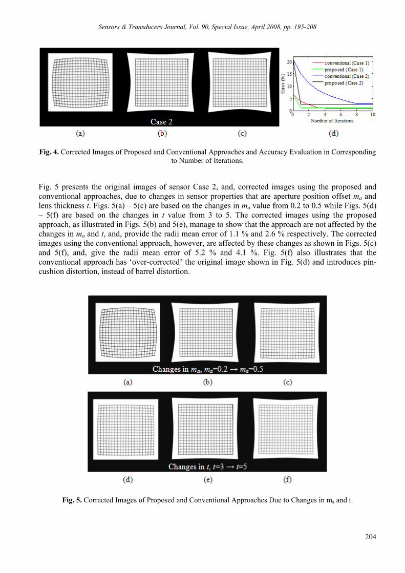
Sensors & Transducers Journal, Vol. 90, Special Issue, April 2008, pp. 195-208
204
Fig. 4. Corrected Images of Proposed and Conventional Approaches and Accuracy Evaluation in Corresponding to Number of Iterations.
Fig. 5 presents the original images of sensor Case 2, and, corrected images using the proposed and conventional approaches, due to changes in sensor properties that are aperture position offset ma and lens thickness t. Figs. 5(a) – 5(c) are based on the changes in ma value from 0.2 to 0.5 while Figs. 5(d) – 5(f) are based on the changes in t value from 3 to 5. The corrected images using the proposed approach, as illustrated in Figs. 5(b) and 5(e), manage to show that the approach are not affected by the changes in ma and t, and, provide the radii mean error of 1.1 % and 2.6 % respectively. The corrected images using the conventional approach, however, are affected by these changes as shown in Figs. 5(c) and 5(f), and, give the radii mean error of 5.2 % and 4.1 %. Fig. 5(f) also illustrates that the conventional approach has ‘over-corrected’ the original image shown in Fig. 5(d) and introduces pin-cushion distortion, instead of barrel distortion.
Fig. 5. Corrected Images of Proposed and Conventional Approaches Due to Changes in ma and t.
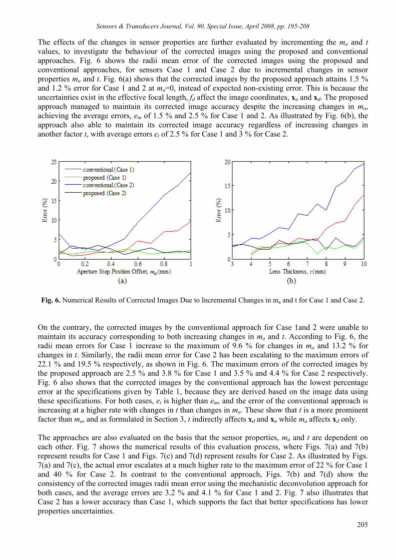
Sensors & Transducers Journal, Vol. 90, Special Issue, April 2008, pp. 195-208
205
The effects of the changes in sensor properties are further evaluated by incrementing the ma and t values, to investigate the behaviour of the corrected images using the proposed and conventional approaches. Fig. 6 shows the radii mean error of the corrected images using the proposed and conventional approaches, for sensors Case 1 and Case 2 due to incremental changes in sensor properties ma and t. Fig. 6(a) shows that the corrected images by the proposed approach attains 1.5 % and 1.2 % error for Case 1 and 2 at ma=0, instead of expected non-existing error. This is because the uncertainties exist in the effective focal length, fd affect the image coordinates, xu and xd. The proposed approach managed to maintain its corrected image accuracy despite the increasing changes in ma, achieving the average errors, em of 1.5 % and 2.5 % for Case 1 and 2. As illustrated by Fig. 6(b), the approach also able to maintain its corrected image accuracy regardless of increasing changes in another factor t, with average errors et of 2.5 % for Case 1 and 3 % for Case 2.
Fig. 6. Numerical Results of Corrected Images Due to Incremental Changes in ma and t for Case 1 and Case 2.
On the contrary, the corrected images by the conventional approach for Case 1and 2 were unable to maintain its accuracy corresponding to both increasing changes in ma and t. According to Fig. 6, the radii mean errors for Case 1 increase to the maximum of 9.6 % for changes in ma and 13.2 % for changes in t. Similarly, the radii mean error for Case 2 has been escalating to the maximum errors of 22.1 % and 19.5 % respectively, as shown in Fig. 6. The maximum errors of the corrected images by the proposed approach are 2.5 % and 3.8 % for Case 1 and 3.5 % and 4.4 % for Case 2 respectively. Fig. 6 also shows that the corrected images by the conventional approach has the lowest percentage error at the specifications given by Table 1, because they are derived based on the image data using these specifications. For both cases, et is higher than em, and the error of the conventional approach is increasing at a higher rate with changes in t than changes in ma. These show that t is a more prominent factor than ma, and as formulated in Section 3, t indirectly affects xd and xu while ma affects xd only. The approaches are also evaluated on the basis that the sensor properties, ma and t are dependent on each other. Fig. 7 shows the numerical results of this evaluation process, where Figs. 7(a) and 7(b) represent results for Case 1 and Figs. 7(c) and 7(d) represent results for Case 2. As illustrated by Figs. 7(a) and 7(c), the actual error escalates at a much higher rate to the maximum error of 22 % for Case 1 and 40 % for Case 2. In contrast to the conventional approach, Figs. 7(b) and 7(d) show the consistency of the corrected images radii mean error using the mechanistic deconvolution approach for both cases, and the average errors are 3.2 % and 4.1 % for Case 1 and 2. Fig. 7 also illustrates that Case 2 has a lower accuracy than Case 1, which supports the fact that better specifications has lower properties uncertainties.

Sensors & Transducers Journal, Vol. 90, Special Issue, April 2008, pp. 195-208
206
Fig. 7. Numerical Results of Image Correction Due to Dynamic Changes in Sensor Properties. The mechanistic deconvolution approach was implemented into a simple image recognition system, to determine its efficiency, in comparison to the previously mentioned conventional approach. The image recognition system consists of two modules, which are the colour and pattern recognition. This system was set in a fixed position and was tested by tracking a red round object in the environment. This experiment was conducted in a controlled environment. Table 2 shows the accuracy and time efficiency of the proposed and conventional approaches. The table indicates that the proposed approach provides low percentage error, averaging at 3.3 %, in contrast to the conventional approach percentage error, averaging at 6.7 %. As stated in Table 2, the proposed approach, is able to provide the corrected image in approximately 5 times faster than the conventional approach in each cycle, which results in increasing the speed performance of the image recognition system by 1.5 times as compared with the conventional approach.
Table 2. Comparison between mechanistic deconvolution and conventional approaches
in image recognition system.
% Error Time (ms) Individual System
Proposed Conventional Proposed Conventional Proposed Conventional Cycle 1 3.5 4.3 10 48 110 150 Cycle 2 2.8 8.3 12 45 107 146 Cycle 3 3.3 9.5 11 50 114 149 Cycle 4 3.8 5.1 13 46 111 151 Cycle 5 3.2 6.2 12 52 109 154
Mean 3.3 6.7 11.6 48.2 110.2 150 5. Conclusion The mechanistic deconvolution approach to modelling an image sensor, without calibration technique, has been presented. The proposed approach has utilized mechanical and electrical properties to determine the effective focal length, and, to estimate the distortion effects inherent in image sensors. This, as a result, has reduced dependency on image data and did not require experimental evaluation of the sensors. Two sensors with different specifications were used to validate the proposed approach, and, the approach managed to provide high accuracy corrected images for the sensors. The proposed approach was then compared with a conventional technique to further evaluate its efficiency. In the efficiency evaluation process, the corrected images derived by the proposed approach achieved accuracy similar to the conventional approach corrected images while considerably reducing the number of iterations.

Sensors & Transducers Journal, Vol. 90, Special Issue, April 2008, pp. 195-208
207
Robustness of the proposed approach due to changes in image sensor properties was also investigated with the conventional technique, and, using two image sensor properties that are the aperture position offset and lens thickness. The model derived by the proposed approach was not affected by the changes of sensor properties, in contrast to the conventional technique. This model, in addition, showed high and consistent accuracy despite incrementing changes of the sensor properties. Thus, it does not require recalibration if sensor parts are modified. The approach was also implemented into a simple image recognition system and proved to be more efficient, in comparison to the conventional technique. In conclusion, the model is not dependent on image data, while successfully correcting for distortion. The assumptions made in the proposed approach, however, have limited the applicability and robustness of the method to dynamic environments. This approach can be extended to include tangential distortion, further improving the accuracy of corrected data. Appendix This section shows brief formulation of the radii mean error. Given the grid pattern of m by n boxes, and, using position indices i=1, 2, n-1, n and j=1, 2, m-1, m, the radii distance for both corrected images dij’ and ideal grid pattern image dij are ( ) ( )2 2
0 0' ' 'ij ij ijd u u v v= - + - (35)
and ( ) ( )2 2
0 0ij ij ijd u u v v= - + - (36)
The [uij, vij] and [uij’, vij’] are the position coordinates of the ideal grid pattern image and corrected images, and, [u0, v0] is the centre position of all images. Using Einstein summation convention, the radii mean error e is '1%Error, 100%ij ij
ij
d de
mn d-
= ґ (37)
References [1]. F. Remondino and C. Fraser, Digital camera calibrations: Considerations and comparisons, International
Archives of Photogrammetry, Remote Sensing and Spatial Information Sciences, 36, 5, 2006, pp. 266-272. [2]. G. N. DeSouza and A. C. Kak, Vision for mobile robot navigation: A Survey, IEEE Transactions on
Pattern Analysis and Machine Intelligence, 24, 2, 2002, pp. 237-267. [3]. R. Y. Tsai, A versatile camera calibration technique for high-Accuracy 3D machine vision metrology using
off-the-Shelf TV cameras and lenses, IEEE Journal of Robotics and Automation, 1987, pp. 323-344. [4]. D. C. Brown, Close-range camera calibration, Photogrammetric Engineering, 37, 8, 1971, pp. 855-866. [5]. J. Weng, P. Cohen and M. Herniou, Camera calibration with distortion models and accuracy evaluation,
IEEE Transactions on Pattern Analysis and Machine Intelligence, 14, 10, 1992, pp. 965-980. [6]. S. Graf and T. Hanning, Analytical solving radial distortion parameters, In Proceedings of the 2005 IEEE
Computer Society International Conference on Computer Vision and Pattern Recognition (CVPR’ 2005), San Diego, CA, USA, 20-25 August 2005, pp. 1104-1109.

Sensors & Transducers Journal, Vol. 90, Special Issue, April 2008, pp. 195-208
208
[7]. J. Mallon and P. F. Whelan, Precise radial un-distortion of images, In Proceedings of the 17th International Conference on Pattern Recognition (ICPR’ 2004), Cambridge, England, UK, 23-26 August 2004, pp. 18-21.
[8]. D. G. Bailey, A new approach to lens distortion correction, In Proceedings Image and Vision Computing New Zealand (IVCNZ’ 2002 0, Auckland, New Zealand, 26-28 November 2002, pp. 59-64.
[9]. S. Park and K. Hong, Practical ways to calculate camera lens distortion for real-time camera calibration, Pattern Recognition, 34, 6, 2004, pp. 1199-1206.
[10].S. J. Maybank and O. D. Faugeras, A theory of self-calibration of a moving camera, International Journal of Computer Vision, 8, 2, 1992, pp. 123-151.
[11]. E. E. Hemayed, A survey of camera self-calibration, In Proceedings of the IEEE Conference on Advanced Video and Signal Based Surveillance (AVSS’2003), Miami, Florida, USA, 21-22 July 2003, pp. 352-357.
[12]. Z. Zhang, A flexible new technique for camera calibration, IEEE Transactions on Pattern Analysis and Machine Intelligence, 22, 11, 2000, pp. 1330-1334.
[13].J. Morgan, Introduction to Geometrical and Physical Optics, R. E. Krieger Pub. Co., 1953. [14]. S. H. Lim and T. Furukawa, Optical Sensor Modelling Using Mechanistic Deconvolution, In The 2nd
International Conference on Sensing Technology (ICST’ 2007), Palmerston North, New Zealand, 26-28 November 2007, pp. 387-392.
___________________
2008 Copyright ©, International Frequency Sensor Association (IFSA). All rights reserved. (http://www.sensorsportal.com)
Sensors & Transducers Journal, Vol. 90, Special Issue, April 2008, pp. 209-220
209
SSSeeennnsssooorrrsss &&& TTTrrraaannnsssddduuuccceeerrrsss
ISSN 1726-5479© 2008 by IFSA
http://www.sensorsportal.com
Functional Link Neural Network-based Intelligent Sensors for Harsh Environments
Jagdish C. Patra1, Goutam Chakraborty2 and Subhas Mukhopadhyay3
1School of Computer Engineering, Nanyang Technological University, Singapore 2Department of Software and Information Sciences, Iwate Prefectural University, Japan
3Department of Electrical & Electronic Engineering, Massey University (Turitea), New Zealand E-mail: [email protected], [email protected], [email protected]
Received: 15 October 2007 /Accepted: 20 February 2008 /Published: 15 April 2008 Abstract: As the use of sensors is wide spread, the need to develop intelligent sensors that can automatically carry out calibration, compensate for the nonlinearity and mitigate the undesirable influence of the environmental parameters, is obvious. Smart sensing is needed for accurate and reliable readout of the measurand, especially when the sensor is operating in harsh environments. Here, we propose a novel computationally-efficient functional link neural network (FLNN) that effectively linearizes the response characteristics, compensates for the nonidealities, and calibrates automatically. With an example of a capacitive pressure sensor and through extensive simulation studies, we have shown that the performance of the FLNN-based sensor model is similar to that of a multilayer perceptron (MLP)-based model although the former has much lower computational requirement. The FLNN model is capable of producing linearized readout of the applied pressure with a full-scale error of only ±1.0% over a wide operating range of −50 to 2000 C. Copyright © 2008 IFSA. Keywords: Smart sensor, Harsh environment, Functional link neural network 1. Introduction We begin by quoting Brian Betts [1]: ”Chances are, your health and happiness rely on sensors, those ubiquitous little devices that tell us if a fridge is too cold, a nuclear reactor’s safety systems are operating, or a factory production line is processing components correctly. But sensors have a dirty little secret: its all too easy for them be in perfect working order, reporting all is well when, in fact, your milk is turning into a frozen block, the reactor’s safety system is impotent, and that factory has filled a warehouse with useless and possibly dangerous products.”
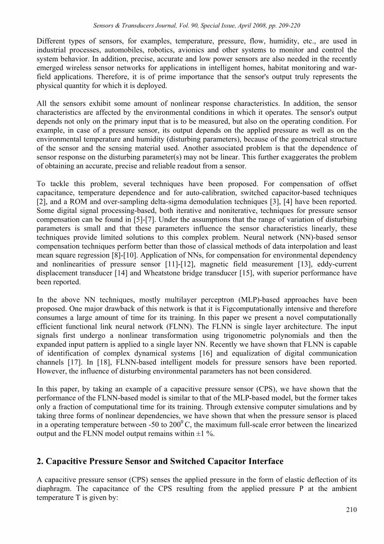
Sensors & Transducers Journal, Vol. 90, Special Issue, April 2008, pp. 209-220
210
Different types of sensors, for examples, temperature, pressure, flow, humidity, etc., are used in industrial processes, automobiles, robotics, avionics and other systems to monitor and control the system behavior. In addition, precise, accurate and low power sensors are also needed in the recently emerged wireless sensor networks for applications in intelligent homes, habitat monitoring and war-field applications. Therefore, it is of prime importance that the sensor's output truly represents the physical quantity for which it is deployed. All the sensors exhibit some amount of nonlinear response characteristics. In addition, the sensor characteristics are affected by the environmental conditions in which it operates. The sensor's output depends not only on the primary input that is to be measured, but also on the operating condition. For example, in case of a pressure sensor, its output depends on the applied pressure as well as on the environmental temperature and humidity (disturbing parameters), because of the geometrical structure of the sensor and the sensing material used. Another associated problem is that the dependence of sensor response on the disturbing parameter(s) may not be linear. This further exaggerates the problem of obtaining an accurate, precise and reliable readout from a sensor. To tackle this problem, several techniques have been proposed. For compensation of offset capacitance, temperature dependence and for auto-calibration, switched capacitor-based techniques [2], and a ROM and over-sampling delta-sigma demodulation techniques [3], [4] have been reported. Some digital signal processing-based, both iterative and noniterative, techniques for pressure sensor compensation can be found in [5]-[7]. Under the assumptions that the range of variation of disturbing parameters is small and that these parameters influence the sensor characteristics linearly, these techniques provide limited solutions to this complex problem. Neural network (NN)-based sensor compensation techniques perform better than those of classical methods of data interpolation and least mean square regression [8]-[10]. Application of NNs, for compensation for environmental dependency and nonlinearities of pressure sensor [11]-[12], magnetic field measurement [13], eddy-current displacement transducer [14] and Wheatstone bridge transducer [15], with superior performance have been reported. In the above NN techniques, mostly multilayer perceptron (MLP)-based approaches have been proposed. One major drawback of this network is that it is Figcomputationally intensive and therefore consumes a large amount of time for its training. In this paper we present a novel computationally efficient functional link neural network (FLNN). The FLNN is single layer architecture. The input signals first undergo a nonlinear transformation using trigonometric polynomials and then the expanded input pattern is applied to a single layer NN. Recently we have shown that FLNN is capable of identification of complex dynamical systems [16] and equalization of digital communication channels [17]. In [18], FLNN-based intelligent models for pressure sensors have been reported. However, the influence of disturbing environmental parameters has not been considered. In this paper, by taking an example of a capacitive pressure sensor (CPS), we have shown that the performance of the FLNN-based model is similar to that of the MLP-based model, but the former takes only a fraction of computational time for its training. Through extensive computer simulations and by taking three forms of nonlinear dependencies, we have shown that when the pressure sensor is placed in a operating temperature between -50 to 2000 C, the maximum full-scale error between the linearized output and the FLNN model output remains within ±1 %. 2. Capacitive Pressure Sensor and Switched Capacitor Interface A capacitive pressure sensor (CPS) senses the applied pressure in the form of elastic deflection of its diaphragm. The capacitance of the CPS resulting from the applied pressure P at the ambient temperature T is given by:

Sensors & Transducers Journal, Vol. 90, Special Issue, April 2008, pp. 209-220
211
),,()(),( 0 TPCTCTPC ∆+= (1)
where ∆C(P, T) is the change in capacitance and C0(T ) is the offset capacitance, i.e., the zero-pressure capacitance, both at the ambient temperature T . The above capacitance may be expressed in terms of capacitances at the reference temperature T0 as: ),(),()()(),( 20100 TfTPCTfTCTPC ∆+= (2) where )( 00 TC is the offset capacitance and ),( 0TPC∆ is the change in capacitance, both at the reference temperature 0T . The nonlinear functions )(1 Tf and )(2 Tf determine the effect of temperature on the sensor characteristics [3]. This model provides sufficient accuracy in determining the influence of temperature on the sensor response characteristics. When pressure is applied to the CPS, its change in capacitance at the reference temperature 0T is given by:
,11)(),( 000
NN P
PTCTPC−−
=∆τ (3)
where τ is a sensitivity parameter, the normalized applied pressure NP is given by ,/ maxPPPN = and
maxP is the maximum permissible applied pressure. The parameters τ and maxP depend on the geometrical structure and physical dimensions of the CPS. The nonlinear functions )(1 Tf ) and )(2 Tf control the influence of the ambient temperature on the CPS characteristics, and are given by: ,1)( 3
32
21 NiNiNii TTTTf κκκ +++= (4) where ,2 and 1=i and the normalized temperature, NT is given by )./()( minmax0 TTTTTN −−= The maximum and the minimum operating temperatures are denoted by maxT and minT , respectively. The coefficients, ijκ determine the extent of temperature influence on the sensor characteristics. Note that when 0=ijκ for j = 2 and 3, the influence of the temperature on the CPS response characteristics is linear. Thus, the normalized capacitance at any temperature T may be expressed as: ),(/),( 00 TCTPCCN = (5) Using (2) and (3) this may be written as: ),()( 21 TfTfCN γ+= (6)
where .11
NN P
P−−
=τγ A schematic diagram of a switched capacitor interface (SCI) for the CPS is
shown in Fig. 1, in which the CPS is shown as C (P). The SCI output provides a voltage signal proportional to capacitance change in the CPS due to the applied pressure. The SCI output voltage is given by: ),(0 PKCV = (7) where ./ SR CVK = By choosing proper values of the reference voltage RV and the reference capacitor
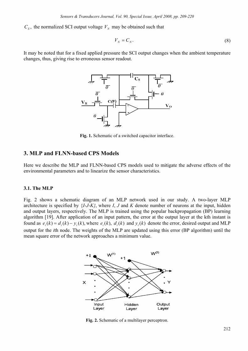
Sensors & Transducers Journal, Vol. 90, Special Issue, April 2008, pp. 209-220
212
,SC the normalized SCI output voltage NV may be obtained such that .NN CV = (8) It may be noted that for a fixed applied pressure the SCI output changes when the ambient temperature changes, thus, giving rise to erroneous sensor readout.
Fig. 1. Schematic of a switched capacitor interface. 3. MLP and FLNN-based CPS Models Here we describe the MLP and FLNN-based CPS models used to mitigate the adverse effects of the environmental parameters and to linearize the sensor characteristics. 3.1. The MLP Fig. 2 shows a schematic diagram of an MLP network used in our study. A two-layer MLP architecture is specified by I-J-K, where I, J and K denote number of neurons at the input, hidden and output layers, respectively. The MLP is trained using the popular backpropagation (BP) learning algorithm [19]. After application of an input pattern, the error at the output layer at the kth instant is found as ),()()( kykdke iii −= where )( and )( ),( kykdke iii denote the error, desired output and MLP output for the ith node. The weights of the MLP are updated using this error (BP algorithm) until the mean square error of the network approaches a minimum value.
Fig. 2. Schematic of a multilayer perceptron.

Sensors & Transducers Journal, Vol. 90, Special Issue, April 2008, pp. 209-220
213
3.2. The FLNN The structure of a FLNN is depicted in Fig. 3. It consists of a functional expansion block and a single layer perceptron network. The main purpose of the functional expansion block is to increase the dimension of the input pattern so as to enhance its representation in a high-dimensional space. This enhanced pattern is then used for modeling of the sensor. Let us denote an m-dimensional input pattern vector at kth instant by: )].( ..., ),( ),([ 21 kxkxkxX mk = (9)
Fig. 3. Schematic of a functional link neural network. Each element of the input vector is expanded into several terms, by using orthogonal trigonometric polynomials. The n-dimensional expanded pattern vector obtained from kX is given by:
...]. )),(sin(2 )),(cos(2 )),(sin( )),(cos( ),( ..., )),(sin(2 )),(cos(2 )),(sin( )),(cos( ),([
22222
11111'
kxkxkxkxkxkxkxkxkxkxX k
ππππππππ=
(10)
Thus, using trigonometric polynomials, the m-dimensional input pattern is enhanced into an n-dimensional (n > m) expanded pattern, which is then applied to a single-layer perceptron. The FLNN schematic shown in Fig. 3, in which m = 2 and n = 9 have been chosen. In addition, sometimes, a few cross-product terms are also included in the expanded pattern, to improve the original pattern representation in the expanded pattern space. The advantage of FLNN over MLP is that the FLNN is computationally more efficient and as such it takes much less time to train than that of the MLP. More details of FLNN may be found in [16], [17], [20]. 3.3. Computational Complexity We present a comparison of computational complexity between MLP and FLNN neural networks, both trained with the BP algorithm. Let us consider a two-layer MLP structure specified by I, J and K number of nodes in the input, hidden and output layers, respectively, excluding the bias units. Whereas, the FLNN has D input nodes and K output nodes. Three basic computations, i.e., addition, multiplication and computation of tanh(.) are involved for updating the weights of the neural networks.

Sensors & Transducers Journal, Vol. 90, Special Issue, April 2008, pp. 209-220
214
For the MLP, the increased computation burden is due to the back error propagation by calculating square error derivative at each node in the hidden layer. In one iteration, all computations in the network take place in three phases: (i) forward calculation to find the activation values of all nodes of the entire network; (ii) back error propagation for calculation of square error derivatives; and (iii) updating of the weights of the whole network. In addition, sin()/cos() computations are required for the FLNN. The total number of weights to be updated in one iteration in the 2-layer MLP is K) J(I K J +++ whereas in case of FLNN it is ) K(D 1+ . It may be seen from Table 1 that as hidden layer does not exist in the FLNN, its computational complexity is much lower than the MLP network. In addition, the FLNN requires fewer numbers of weights to achieve similar performance as that of MLP.
Table 1. Comparison of computational complexity between MLP and FLNN.
Operation MLPI-J-K FLNN D-KAddition 4IJ + 3JK 3K(D+1)
Multiplication 6J(I+K) 6K(D+1) tanh() J+K K
cos()/ sin() - D 3.4. NN-based Sensor Model A schematic diagram of the NN-based CPS model is provided in Fig. 4. The ambient temperature and the SCI output are used as inputs to the NN. Appropriate scale factors (SFs) are used to keep these values within 1.0. The desired output is the linearized normalized voltage. During the training phase, an input pattern from the training set is applied to the NN and its weights are updated using BP algorithm. At the end of training, the final weights are stored in an EEPROM. During the second phase, the test phase, the stored final weights are loaded into the MLP. An input pattern from the test set is applied to the NN model and its output is computed. If the NN output and the target output match closely, then it may be said that the NN model has learnt the sensor characteristics satisfactorily. To illustrate the effectiveness of the NN model to compensate for the nonlinear dependency of temperature on sensor characteristics, three forms of nonlinear functions denoted by NL1, NL2 and NL3 have been selected. A linear function denoted by NL0 is also used for comparison purposes. These nonlinear functions are generated by using different sets of coefficients ijκ in Eq. (4). In this study, the temperature information is assumed to be available. It can be obtained by using a temperature sensor. We carried out two sets of experiments by two implementations of the NN-block as shown in Fig. 4, namely, MLP and FLNN, and compared their performances.
Fig. 4. NN-based CPS modeling.

Sensors & Transducers Journal, Vol. 90, Special Issue, April 2008, pp. 209-220
215
4. Simulation Studies Here we provide the details of the simulation studies carried out for performance evaluation of the proposed MLP and FLNN-based CPS models. 4.1. Preparation of Datasets All the parameters of the CPS, e.g., the ambient temperature, the applied pressure, and the SCI output voltage, were suitably normalized to keep their values within ±1.0. The SCI output voltage NV was recorded at the reference temperature ( CT 0
0 25= ) with different known values of normalized pressure ( NP ) chosen between 0.0 and 0.6 at intervals of 0.05. Thus, these 13 pairs of data ( NN VP versus ) constitute one dataset at the reference temperature. To study the influence of temperature on the CPS characteristics, three forms of nonlinear functions NL1, NL2, and NL3, and a linear form NL0 were generated by selecting proper values of ijκ in Eq.(4). The selected values of the ijκ are tabulated in Table 2.
Table 2. The selected values of ijκ for different nonlinear dependencies.
NL form
131211 κκκ 232221 κκκ NL0 0.10 0.00 0.00 0.20 0.00 0.00 NL1 0.25 -0.25 0.10 0.20 -0.40 0.40 NL2 0.30 0.10 -0.30 0.20 -0.20 -0.10 NL3 0.40 -0.15 -0.15 0.25 0.30 -0.60
Next, with the knowledge of the dataset at the reference temperature and the chosen values of ijκ , the response characteristics of the CPS for a specific ambient temperature were generated using Eq. (6). The response characteristics consist of 13 pairs of data ( NN VP versus ), and correspond to a dataset at a specific temperature. For temperature from −50 to 2000C, at an increment of 100C, twenty-six such datasets, each containing 13 data pairs, were generated. Next, these datasets were divided into two groups: the training set and the test set. The training set, used for training the NNs, consists of only five datasets corresponding to −50, 10, 70, 130 and 1900C, and the remaining twenty one datasets were used as the test set. The sensor characteristics for the linear (NL0) and nonlinear (NL1) dependencies at different temperatures and the desired linear response are plotted in Fig. 5. It can be seen that the response characteristics of the sensor change nonlinearly over the temperature range. Besides, the change in response characteristics differs substantially for different forms of nonlinear dependencies. However, it is important to note that, in order to have accurate and precise sensor readout, it should provide linear readout of the applied pressure in spite of the nonlinear sensor characteristics, changes in ambient temperature and nonlinear temperature dependency.

Sensors & Transducers Journal, Vol. 90, Special Issue, April 2008, pp. 209-220
216
Fig. 5. Desired linear characteristics and SCI output, i.e., the CPS response characteristics operating at different
temperatures (−50, 0, 25, 100, and 2000C): (a) NL0; (b) NL1.
4.2. Training and Testing of NN Models A 2-layer MLP with 2-5-1 architecture was chosen in this modeling problem (see Fig. 2). Thus, the number of nodes including the bias units in the input, hidden and the output layers are 3, 6 and 1, respectively. This MLP contains only 21 weights. Its two inputs are the normalized temperature ( NT ), and the normalized SCI output voltage ( NV ). The linear normalized voltage, LinV was used as the target output for the MLP. Initially, all the weights of the MLP were set to some random values within ±0.5. During training, the five datasets were chosen randomly. The learning parameter α and the momentum factor β used in the BP algorithm, were selected as 0.3 and 0.5, respectively. For effective learning, 50,000 iterations were run to train the MLP model. To improve learning of the NN, the learning parameter was varied with iteration number. In the case of FLNN, the 2-dimensional input pattern was expanded into 14-dimensional pattern by using trigonometric polynomials (10). Both the learning parameter and the momentum factor were chosen as 0.5. The training was continued for 50,000 iterations. Using a Pentium, 1.10 GHz machine, it took 12 seconds to train the MLP, whereas in case of the FLNN it took only 9 seconds. Note that the number of weights in the MLP and FLNN are 21 and 14, respectively.
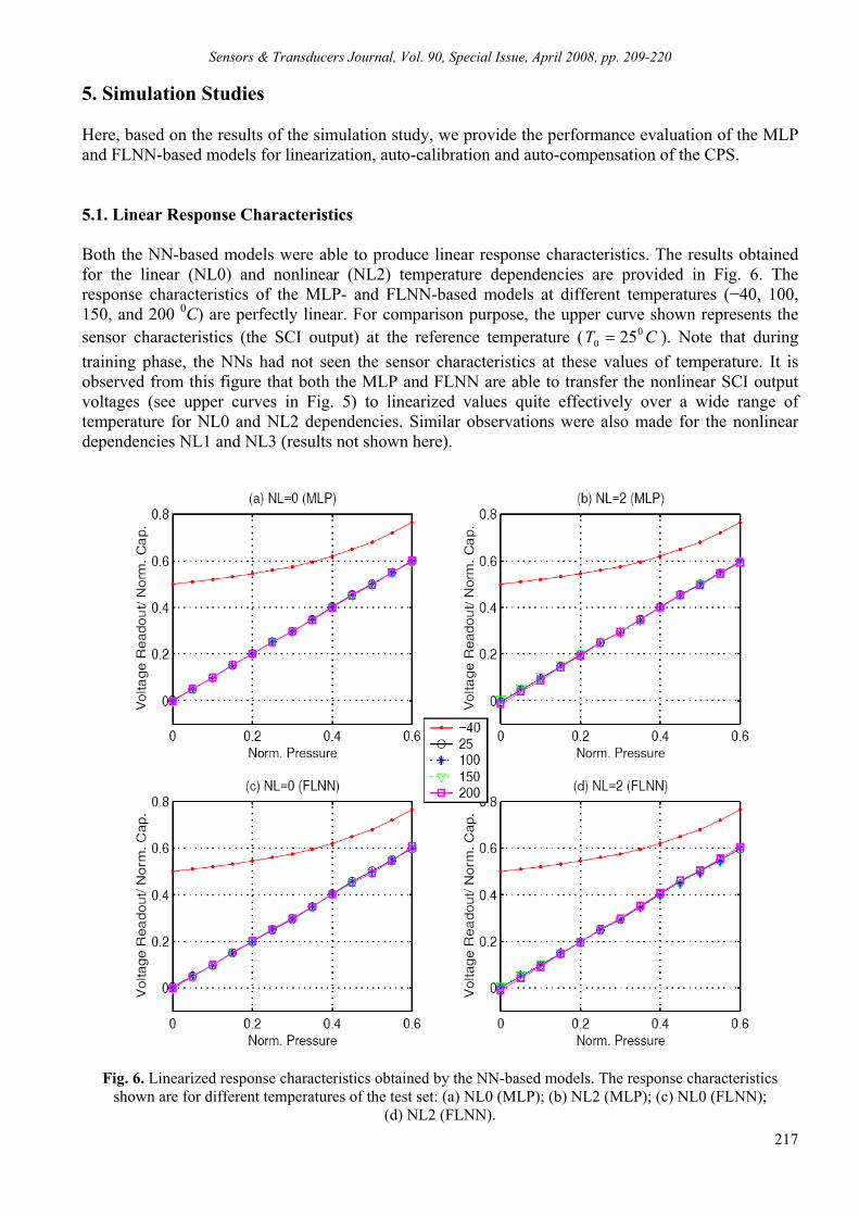
Sensors & Transducers Journal, Vol. 90, Special Issue, April 2008, pp. 209-220
217
5. Simulation Studies Here, based on the results of the simulation study, we provide the performance evaluation of the MLP and FLNN-based models for linearization, auto-calibration and auto-compensation of the CPS. 5.1. Linear Response Characteristics Both the NN-based models were able to produce linear response characteristics. The results obtained for the linear (NL0) and nonlinear (NL2) temperature dependencies are provided in Fig. 6. The response characteristics of the MLP- and FLNN-based models at different temperatures (−40, 100, 150, and 200 0C) are perfectly linear. For comparison purpose, the upper curve shown represents the sensor characteristics (the SCI output) at the reference temperature ( CT 0
0 25= ). Note that during training phase, the NNs had not seen the sensor characteristics at these values of temperature. It is observed from this figure that both the MLP and FLNN are able to transfer the nonlinear SCI output voltages (see upper curves in Fig. 5) to linearized values quite effectively over a wide range of temperature for NL0 and NL2 dependencies. Similar observations were also made for the nonlinear dependencies NL1 and NL3 (results not shown here).
Fig. 6. Linearized response characteristics obtained by the NN-based models. The response characteristics shown are for different temperatures of the test set: (a) NL0 (MLP); (b) NL2 (MLP); (c) NL0 (FLNN);
(d) NL2 (FLNN).
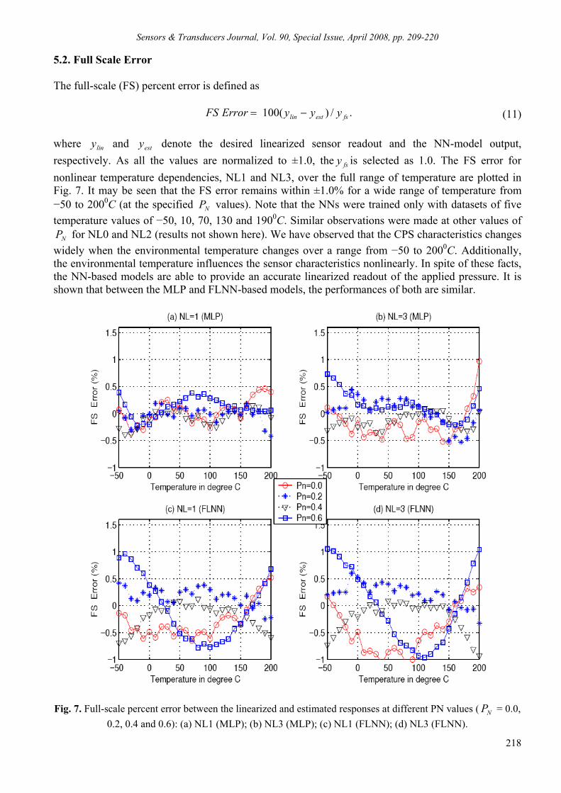
Sensors & Transducers Journal, Vol. 90, Special Issue, April 2008, pp. 209-220
218
5.2. Full Scale Error The full-scale (FS) percent error is defined as ./)(100 fsestlin yyy ErrorFS −= (11) where liny and esty denote the desired linearized sensor readout and the NN-model output, respectively. As all the values are normalized to ±1.0, the fsy is selected as 1.0. The FS error for nonlinear temperature dependencies, NL1 and NL3, over the full range of temperature are plotted in Fig. 7. It may be seen that the FS error remains within ±1.0% for a wide range of temperature from −50 to 2000C (at the specified NP values). Note that the NNs were trained only with datasets of five temperature values of −50, 10, 70, 130 and 1900C. Similar observations were made at other values of
NP for NL0 and NL2 (results not shown here). We have observed that the CPS characteristics changes widely when the environmental temperature changes over a range from −50 to 2000C. Additionally, the environmental temperature influences the sensor characteristics nonlinearly. In spite of these facts, the NN-based models are able to provide an accurate linearized readout of the applied pressure. It is shown that between the MLP and FLNN-based models, the performances of both are similar.
Fig. 7. Full-scale percent error between the linearized and estimated responses at different PN values ( NP = 0.0,
0.2, 0.4 and 0.6): (a) NL1 (MLP); (b) NL3 (MLP); (c) NL1 (FLNN); (d) NL3 (FLNN).
Sensors & Transducers Journal, Vol. 90, Special Issue, April 2008, pp. 209-220
219
5. Conclusions A novel NN-based smart sensor that is capable of providing linearized readout, auto-calibration and auto-compensation for the nonlinear influence of the environmental parameters on its characteristics, has been proposed. By taking an example of a capacitive pressure sensor, we have shown that the proposed computationally efficient FLNN model provides satisfactory performance even when it is operating in a harsh environment. We have shown the effectiveness of the FLNN-based model with computer simulated experiments for different forms of nonlinear temperature dependences for a temperature range between −50 to 2000C. The maximum error between the ideal linearized output and the NN model remains within ±1.0% (FS) for both the NN-based models, though the MLP’s FS error is slightly better. However, the FLNN-based model takes less time for its training due its single-layer structure. The FLNN needs less number of weights to achieve similar performance as that of MLP. Such NN-based models, especially, the FLNN, may be applied to other types of sensors to achieve linearized readout, auto-calibration and to mitigate the nonlinear influence of the environmental parameters on their response characteristics. References [1]. B. Betts, Smart sensors, IEEE Spectrum, 43, 4, 2006, pp.50-53. [2]. X. Li and G. C. Meijer, An accurate interface for capacitive sensors, IEEE Trans. Instrum. and Meas.,
2002, pp. 935-939. [3]. M. Yamada, T. Takebayashi, S-I. Notoyama, and K. Watanabe, A switched-capacitor interface for
capacitive pressure sensors, IEEE Trans. Instrum. and Meas., 1992, pp. 81-86. [4]. M. Yamada and K. Watanabe, A capacitive pressure sensor interface using oversampling Σ−∆
demodulation techniques, IEEE Trans. Instrum. and Meas., 1997, pp. 3-7. [5]. P. Hille, R. Hohler, and H. Strack, A linearization and compensation method for integrated sensors, Sensors
and Actuators-B, 1994, pp. 95-102. [6]. I. Maric, Automatic digital correction of measurement data based on M-point autocalibration and inverse
polynomial approximation, IEEE Trans. Industrial Electronics, 1988, pp. 317-322. [7]. K. F. Lyahou, G. van der Horn, and J. H. Huijsing, A noniterative polynomial 2-D calibration method
implemented in a microcontroller, IEEE Trans. Instrum. and Meas., 1997, pp. 752-757. [8]. J. M. Dias Pereira, P. M. B. Silva Girao, and O. Postolache, Fitting transducer characteristics to measured
data, IEEE Instrum. and Meas. Magazine, 2001, pp. 26-39. [9]. R. Z. Morawski, Digital signal processing in measurement microsystems, IEEE Instrum. and Meas.
Magazine, 2004, pp. 43-50. [10]. A. P. Singh, S. Kumar and T. S. Kamal, Fitting transducer characteristics to measured data using a virtual
curve tracer, Sensors and Actuators A, 2004, pp. 145- 153. [11]. J. C. Patra, A. van den Bos, and A. C. Kot, An NN-based smart capacitive pressure sensor in dynamic
environment, Sensors and Actuators-B, 2000, pp. 26-38. [12]. J. C. Patra, E. L. Ang, N. S. Chaudhari and A. Das, Neural- network-based smart sensor framework
operating in a harsh environment, Journal of Applied Signal Processing, 2005, pp. 558-574. [13]. J. M. Dias Pereira, O. Postolache, and P. M. B. Girao, A temperature compensated system for magnetic
field measurements based on artificial neural networks, IEEE Trans. Instrum. and Meas., 1998, pp. 494-498.
[14]. P. Arpaia, P. Daponte, D. Grimaldi, and L. Michaeli, ANN-based error reduction for experimentally modeled sensors, IEEE Trans. Instrum. and Meas., 2002, pp. 23-30.
[15]. A. P. Singh, S. Kumar and T. S. Kamal, Development of ANN-based virtual fault detector for Wheatstone bridge-oriented transducer, IEEE Sensors Journal, 2005, pp. 1043-1049.
[16]. J.C. Patra, R. N. Pal, B. N. Chatterji and G. Panda, Identification of nonlinear dynamic systems using functional link artificial neural networks, IEEE Trans. Systems, Man and Cybernetics, Part-B, 1999, pp. 254-262.
[17]. J.C. Patra, R. N. Pal, R. Baliarsingh and G. Panda, Nonlinear channel equalization for QAM signal constellation using artificial neural networks, IEEE Trans. Systems, Man and Cybernetics, Part-B, 1999, pp. 262-271.

Sensors & Transducers Journal, Vol. 90, Special Issue, April 2008, pp. 209-220
220
[18]. J. C. Patra and A. van den Bos, Modeling of an intelligent pressure sensor using functional link artificial neural networks, ISA Transactions, 2000, pp. 15-27.
[19]. S. Haykin, Neural Networks, Maxwell MacMillan, Ontario, Canada, 1994. [20]. Y. -H. Pao, Adaptive Pattern recognition and Neural Networks, Reading, MA, Addison-Wesley, 1989.
___________________ 2008 Copyright ©, International Frequency Sensor Association (IFSA). All rights reserved. (http://www.sensorsportal.com)
UUnniivveerrssaall FFrreeqquueennccyy--ttoo--DDiiggiittaall CCoonnvveerrtteerr ((UUFFDDCC--11))
•• 1166 mmeeaassuurriinngg mmooddeess:: ffrreeqquueennccyy,, ppeerriioodd,, iittss ddiiffffeerreennccee aanndd rraattiioo,, dduuttyy--ccyyccllee,, dduuttyy--ooffff ffaaccttoorr,, ttiimmee iinntteerrvvaall,, ppuullssee wwiiddtthh aanndd ssppaaccee,, pphhaassee sshhiifftt,, eevveennttss ccoouunnttiinngg,, rroottaattiioonn ssppeeeedd
•• 22 cchhaannnneellss •• PPrrooggrraammmmaabbllee aaccccuurraaccyy uupp ttoo 00..000011 %% •• WWiiddee ffrreeqquueennccyy rraannggee:: 00..0055 HHzz ……77..55 MMHHzz
((112200 MMHHzz wwiitthh pprreessccaalliinngg)) •• NNoonn--rreedduunnddaanntt ccoonnvveerrssiioonn ttiimmee •• RRSS--223322,, SSPPII aanndd II22CC iinntteerrffaacceess •• OOppeerraattiinngg tteemmppeerraattuurree rraannggee --4400 00CC……++8855 00CC
www.sensorspor.com [email protected] SWP, Inc., Canada

Sensors & Transducers Journal, Vol. 90, Special Issue, April 2008, pp. 221-232
221
SSSeeennnsssooorrrsss &&& TTTrrraaannnsssddduuuccceeerrrsss
ISSN 1726-5479© 2008 by IFSA
http://www.sensorsportal.com
MEMS Based Pressure Sensors – Linearity and Sensitivity Issues
1Jaspreet Singh, 1K. Nagachenchaiah, 2M. M. Nayak
1Semiconductor Laboratory(SCL), Dept. of Space, Punjab, India 2Liquid Propulsion System Centre (LPSC), ISRO, Dept. of Space, Bangalore, India
E-mail: [email protected], [email protected], [email protected]
Received: 15 October 2007 /Accepted: 20 February 2008 /Published: 15 April 2008 Abstract: This paper describes the various nonlinearities (NL) encountered in the Si-based Piezoresistive pressure sensors. The effect of various factors like diaphragm thickness, diaphragm curvature, position of the piezoresistors etc. is analyzed taking anisotropy into account. Also, the effect of modified bending stiffness due to presence of oxide/nitride used for isolation between metal and diaphragm is studied from linearity point of view. Copyright © 2008 IFSA. Keywords: Pressure sensor, Sensitivity, Linearity, Piezoresistance, Wheatstone bridge 1. Introduction MEMS based Pressure sensors are mechanically similar to traditional sensors with the exception that these are Si based and on micrometer scale. The additional advantages of MEMS based pressure sensors include batch fabrication, high performance, small size, low cost, absence of adhesive bonding layer and easy integration with electronics on single chip. Pressure sensors have a wide-range of applications in various fields like automotive industry, biomedical, space applications and military applications. These pressure sensors are available in wide operating range covering from fractions of psi to 15,000 psi. A lot of research has been carried out on micromachined piezoresistive pressure sensors in the recent years [1-4]. For high performance demands, the sensitivity and linearity must be improved. In order to increase the sensitivity, the diaphragm thickness should be thin. In present commercial Piezoresistive pressure sensors, Si diaphragms with less than 20 µm thickness are common [5]. Generally thin diaphragms are prone to large deflections and nonlinear effects. It is therefore necessary to optimize

Sensors & Transducers Journal, Vol. 90, Special Issue, April 2008, pp. 221-232
222
the diaphragm thickness with respect to rigidity and strength. Nonlinear higher order piezoresistance coefficients add-up the linearity error further. Proper selection of piezoresistors i.e. orientation, shape, location, doping concentration, dose etc. is essential. Finally the conversion of small resistance change to voltage output is another additive nonlinearity. This paper reviews the types of nonlinearities in the context of Piezoresistive pressure sensors, giving basic relationships between pressure, stress, deflection, and resistance change and voltage output. The results of numerical simulations of square diaphragm for optimum load-deflection are presented. 2. Nonlinearities in Piezoresistive Pressure Sensor A Piezoresistive pressure sensor consists of a diaphragm with diffused piezoresistors in Wheatstone bridge configuration (Fig. 1). The diaphragm converts pressure into mechanical stress, the piezoresistors converts this stress into resistance change and finally the resistance change is converted the into output voltage. These subsystems have to be considered and optimized in order to realize a pressure sensor with high sensitivity and good linearity. Nonlinearity of a transducer can be defined as the maximum deviation of the calibration curve from specified best fit straight line. Mathematically, overall non-linearity for Piezoresistive pressure transducer can be given as [5]
rprddp NLNLNLNL ,2
,2
,2 ++= , (1)
where NLp,d is the nonlinearity between pressure-deflection (structural nonlinearity), NLd,r is the nonlinearity between deflection-resistance (piezoresistive nonlinearity) and NLp,r is the non-linearity due to difference in the sensitivities to pressure among resistors (bridge nonlinearity). In what follows, these nonlinearities are discussed in some detail.
Fig. 1. Principle of Piezoresistive pressure sensor.
3. Structural Nonlinearity Consider a thin silicon plate subjected to an applied pressure p resulting in lateral bending. The governing differential equation can be written as [6]
pyM
yxM
xM yxyx −=
∂
∂+
∂∂
∂−
∂∂
2
22
2
2
2 (2)
The above equation (2) can be written in terms of load-deflection form as

Sensors & Transducers Journal, Vol. 90, Special Issue, April 2008, pp. 221-232
223
Dp
yw
yxw
xw
=∂∂
+∂∂
∂+
∂∂
4
4
22
2
4
4
2 , (3)
where w(x, y) is the deflection which can be found by solving (3) with proper boundary conditions. D refers to flexural rigidity assuming the constant plate thickness, h. Various numerical techniques [7-8] are available to solve such equations with proper boundary conditions. The bending strains at the surface can be written as:
yxwh
ywh
xwh
xy
yy
xx
∂∂∂
−=
∂∂
−=
∂∂
−=
2
2
2
2
2
2
2
ε
ε
ε
(4)
Using constitutive equations, the stresses can be found as:
⎟⎟⎠
⎞⎜⎜⎝
⎛∂∂
∂=
⎟⎟⎠
⎞⎜⎜⎝
⎛∂∂
+∂∂
−=
⎟⎟⎠
⎞⎜⎜⎝
⎛∂∂
+∂∂
−=
yxwhG
xw
ywhE
yw
xwhE
xy
yy
xx
2
2
2
2
2
2
2
2
2
2
2
)1(2
)1(2
τ
υυ
σ
υυ
σ
(5)
The above description is just a summary of general practice used for calculating stresses and deflection of a square plate clamped at the edges. The detailed analysis is based on small deflection theory. It assumes that the stress distribution is a result of pure bending i.e. neutral plane of the diaphragm is not stretched. This assumption requires that the deflection of the diaphragm be small when compared with its thickness (w≤0.4h). For thin diaphragms, generally encountered in pressure sensors, this analysis is not sufficient. In case of thin diaphragm, if deflection is not small, neutral plane of the diaphragm will also stretch like a balloon. It is called “balloon effect” [14]. The stress caused by the stretch of neutral plane has to be considered in that case.
Fig. 2. Plate subjected to uniform pressure load.

Sensors & Transducers Journal, Vol. 90, Special Issue, April 2008, pp. 221-232
224
The factors that are contributing to structural nonlinearity can be grouped as (i) Geometric nonlinearity (ii) Material nonlinearity (iii) Contact nonlinearity Geometric nonlinearity occurs when there are large displacements under specified loading conditions. In these cases the small deflection theory is not sufficient to give the deformation behaviour of the plate in full working range. Now strain displacement relations are no longer linear:
⎟⎟⎠
⎞⎜⎜⎝
⎛∂∂
∂∂
+⎟⎟⎠
⎞⎜⎜⎝
⎛∂∂
+∂∂
=
⎟⎟⎠
⎞⎜⎜⎝
⎛∂∂
+∂∂
=
⎟⎠⎞
⎜⎝⎛∂∂
+∂∂
=
yw
xw
xv
yu
yw
yv
xw
xu
xy
yy
xx
.
21
21
2
2
ε
ε
ε
,
(6)
where u, v and w are displacements in x, y and z directions respectively. In this case the stress in diaphragm consists of two parts: the first caused by bending of the diaphragm and second stress caused by the stretch of neutral plane. Mathematically, stretchbending σσσ += (7) Here the load (pressure) is shared by the stretch action also, so bending stress will reduce as compare to the value calculated by small deflection theory. Fig. 3 shows simulation results of linearity error with and without accounting the effect of large deflections for a square diaphragm of width 1054 µm and 10 µm thickness used for 1 bar pressure sensor. The analysis is done using ANSYS [8]. As can be seen, the effect of large deflections is quiet high in this case. The curve is now no longer symmetrical with respect to central point. So the diaphragm is redesigned with optimum dimensions for the same pressure range. Fig. 4 shows the results of linearity error with modified dimensions of 16 µm thickness. The reduction in output signal can be suitably taken care of in the electronic signal processing subject to meeting the sensitivity requirements.
Fig. 3. Linearity error (structural) with and without considering large deflection effect.

Sensors & Transducers Journal, Vol. 90, Special Issue, April 2008, pp. 221-232
225
Fig. 4. Linearity (structural) error for two different thicknesses of the diaphragm. Material non-linearity should be ideally zero in case of single crystal Si diaphragms as the stress-strain relation is linear up to fracture point. However, residual stresses of the fabrication process like deposition/growth, implantation and anisotropic etching etc. contribute to the nonlinearity. Some of these stresses can be relieved during fabrication process itself like drive-in, annealing etc. However complete removal of the stress is not always possible since these are not completely known- qualitatively and quantitatively. Thus the total stress in diaphragm will be: residualbending σσσ ±= (8) It is found [10] that tensile residual stresses increase the bending stiffness (higher stress leads to higher stiffness) of the plate while compressive residual stresses reduce the stiffness and could eventually lead to buckling. This effect was investigated by simulating the diaphragm with grown oxide (having compressive stress) and with both oxide and CVD nitride (CVD Nitride has tensile stress) [10]. It is seen from Fig. 5 that the effect of 0.1 micron grown oxide is negligible as compare to bare Si diaphragm (without oxide). The output increases due to compressive stress and also the structural nonlinearity by about 0.02% FSO. Similarly the effect of Oxide/Nitride layer on the diaphragm is shown in Fig. 6. It shows the degradation of both linearity as well as output as compare to only oxide layer. Contact Non-linearity arises due to change in boundary conditions. Since edges are assumed to be built-in, in case of thin diaphragm this nonlinearity is negligible compared to the other two described earlier.
-0.5
-0.4
-0.3
-0.2
-0.1
0
0.1
0.2
0.3
0.4
0 0.2 0.4 0.6 0.8 1presure(bar)
Line
arity
err
or(%
FSO
)
Without oxidewith 1500A Oxide
Fig. 5. Linearity (structural) error with and without oxide.

Sensors & Transducers Journal, Vol. 90, Special Issue, April 2008, pp. 221-232
226
-4.0
-3.0
-2.0
-1.0
0.0
1.0
2.0
3.0
0 0.2 0.4 0.6 0.8 1pressure(bar)
Non
-Lin
earit
y(%
FSO
)
400/800 oxide nitridewith 1500A oxide
Fig. 6. Linearity error with and without oxide/nitride combination. The polarity (+ve or –ve) of curvature has also effect on the overall sensor nonlinearity. It is seen (Fig. 7) that the application of pressure on the rear side of the diaphragm gives more nonlinearity as compared to the front side application. As the resistors are implanted on the top surface of the diaphragm with approximately 1 µm depth, these can be assumed as surface resistors. ∆R/R is mainly due to the stress distribution over the resistor area. When the pressure is applied from the top side of the diaphragm, the resistors experience the tensile stress (conventionally taken as +ve). So, the ∆R/R is +ve for longitudinal resistor and –ve for transverse resistor. The reverse effect is seen when the pressure is applied from rear side. Secondly, the longitudinal ∆R/R is generally more than the transverse one. However, for linearity, the longitudinal and transverse ∆R/Rs should be equal in magnitude. These two factors increase the overall nonlinear response of the device when pressure is applied from rear side.
Fig. 7. Nonlinearity comparison for front and rear side pressure application. 4. Piezoresistive Nonlinearity For a diffused piezoresistor subjected to parallel and perpendicular stress components, the resistance change is given by
ttllRR σσ
ρρ
∏+∏=∆
≈∆
, (9)
where Пl and Пt are piezoresistive coefficients parallel and perpendicular to the resistor length. This relation assumes that stress levels are relatively small and hence Piezoresistive coefficients of Silicon are independent of stress i.e. when stresses are linear with applied pressure, resistance change will be

Sensors & Transducers Journal, Vol. 90, Special Issue, April 2008, pp. 221-232
227
linear with stress. But, in actual practice extra amount of nonlinearity is observed. This nonlinearity is due to the dependence of piezoresistive coefficients on the stress. However, investigation of the dependence of piezoresistive coefficient on stress is quite involved as there are many components of stress tensor and the measurement of higher order effects requires very high accuracy. The magnitude of this nonlinearity is proportional to the stress value. It has been investigated [12] that nonlinear Piezoresistive coefficients up to third order can play major role in certain crystallographic directions. Up to first order П11, П12 and П 44 can give Пl and Пt for any arbitrary direction in the crystal. These three coefficients further are functions of doping concentration and temperature. But for second order, nine more such piezoresistance components are needed to calculate Пl and Пt. The observation of Matsuda et al [12], for p-type resistors oriented in <110> orientations with a doping level of 2x10¹⁸/cm3, the dependence of nonlinearity on stress is shown in Fig. 8.
Fig. 8. Nonlinearity of p-type piezoresistors for <110> stress (doping level: 2x10¹⁸/cm3).
As can be seen, the nonlinearity due to piezoresistive effect for longitudinal resistor is positive for both tensile and compressive bending stresses whereas for transverse resistor, NL is negative for compressive and positive for tensile stresses. It is found that third order polynomial approximation gives fairly good match [14]. Based on this, one of the techniques adopted for reducing this nonlinearity is by using only transverse piezoresistors instead of both transverse and longitudinal piezoresistors. The effect Piezoresistive nonlinearity is seen by diffusing suitable resistors on the diaphragm in full Wheatstone configuration. It was observed that “structural” nonlinearity is partially compensated by the nonlinearity of the Piezoresistive effect. Fig. 9 shows how structural linearity error changes from 0.37 % to 0.23 % FSO for 16 µm diaphragm with piezoresistors.
-0.5
-0.4
-0.3
-0.2
-0.1
0
0.1
0.2
0.3
0.4
0 0.2 0.4 0.6 0.8 1
pressure(bar)
Non
linea
rity(
%FS
O)
structural NL
structural+PiezoresitiveNL
Fig. 9. Structural NL and Overall NL for 0-1bar pressure sensor.

Sensors & Transducers Journal, Vol. 90, Special Issue, April 2008, pp. 221-232
228
5. Bridge Nonlinearity When an external pressure is applied, the diaphragm is stressed and the longitudinal and transverse resistors undergo different changes in resistances due to the average stresses being different in each resistor. The expression for the resistance change is given in equation (9). Generally, all the four resistors are connected in Wheatstone bridge – either full active or partial. Considering full Wheatstone bridge configuration the output voltage can be calculated as: ( ) ( )
( ) ( )tl
tl
s
o
RRRRRRRR
VV
∆+∆+∆−∆
=2
(10)
Ideally, in a linear voltage output bridge the output is proportional to the deflection of the membrane and hence to the applied pressure. The denominator of the above expression (10) introduces nonlinearity which can be eliminated by designing the resistors such that
tl RR
RR
⎟⎠⎞
⎜⎝⎛ ∆=⎟
⎠⎞
⎜⎝⎛ ∆ (11)
i.e. sensitivity among the piezoresistors should be same. If the above condition is met then the expression for the output voltage ratio is equal to the fractional change in piezoresistance of the resistors. This nonlinearity can be understood by considering the linear but different resistance change with pressure in longitudinal and transverse piezoresistors. The change in resistance is given by
pRR
pRR
t
l
β
α
−=⎟⎠⎞
⎜⎝⎛ ∆
=⎟⎠⎞
⎜⎝⎛ ∆
, (12)
where α, β denotes the sensitivities of the resistors respectively. Substituting (11) in (9), and assuming offset voltage of the bridge is zero, the output voltage (V0) is
so Vp
pV)(2
)(βα
βα−+
+= (13)
The end point nonlinearity at a specific test pressure pi can be given as
100)(
)()(
)(% xpV
pppV
pVFSONL
mo
im
moio
i
−= (14)
Substituting (12) in (13) and assuming maximum nonlinearity for the whole operation range is at pi = pm/2, i.e. half of maximum applied pressure (pm), the NL will be
100)(4)(
2)(% x
pp
FSONLm
m⎥⎦
⎤⎢⎣
⎡−+−
=βαβα (15)
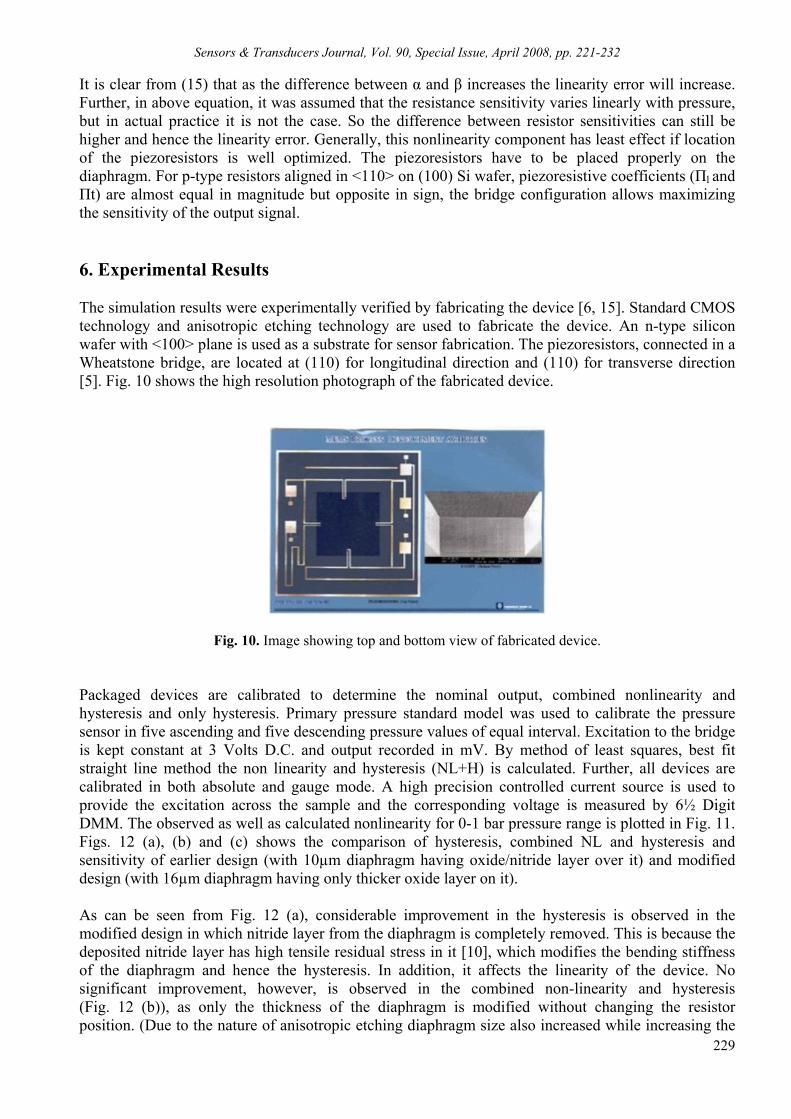
Sensors & Transducers Journal, Vol. 90, Special Issue, April 2008, pp. 221-232
229
It is clear from (15) that as the difference between α and β increases the linearity error will increase. Further, in above equation, it was assumed that the resistance sensitivity varies linearly with pressure, but in actual practice it is not the case. So the difference between resistor sensitivities can still be higher and hence the linearity error. Generally, this nonlinearity component has least effect if location of the piezoresistors is well optimized. The piezoresistors have to be placed properly on the diaphragm. For p-type resistors aligned in <110> on (100) Si wafer, piezoresistive coefficients (Пl and Пt) are almost equal in magnitude but opposite in sign, the bridge configuration allows maximizing the sensitivity of the output signal. 6. Experimental Results The simulation results were experimentally verified by fabricating the device [6, 15]. Standard CMOS technology and anisotropic etching technology are used to fabricate the device. An n-type silicon wafer with <100> plane is used as a substrate for sensor fabrication. The piezoresistors, connected in a Wheatstone bridge, are located at (110) for longitudinal direction and (110) for transverse direction [5]. Fig. 10 shows the high resolution photograph of the fabricated device.
Fig. 10. Image showing top and bottom view of fabricated device. Packaged devices are calibrated to determine the nominal output, combined nonlinearity and hysteresis and only hysteresis. Primary pressure standard model was used to calibrate the pressure sensor in five ascending and five descending pressure values of equal interval. Excitation to the bridge is kept constant at 3 Volts D.C. and output recorded in mV. By method of least squares, best fit straight line method the non linearity and hysteresis (NL+H) is calculated. Further, all devices are calibrated in both absolute and gauge mode. A high precision controlled current source is used to provide the excitation across the sample and the corresponding voltage is measured by 6½ Digit DMM. The observed as well as calculated nonlinearity for 0-1 bar pressure range is plotted in Fig. 11. Figs. 12 (a), (b) and (c) shows the comparison of hysteresis, combined NL and hysteresis and sensitivity of earlier design (with 10µm diaphragm having oxide/nitride layer over it) and modified design (with 16µm diaphragm having only thicker oxide layer on it). As can be seen from Fig. 12 (a), considerable improvement in the hysteresis is observed in the modified design in which nitride layer from the diaphragm is completely removed. This is because the deposited nitride layer has high tensile residual stress in it [10], which modifies the bending stiffness of the diaphragm and hence the hysteresis. In addition, it affects the linearity of the device. No significant improvement, however, is observed in the combined non-linearity and hysteresis (Fig. 12 (b)), as only the thickness of the diaphragm is modified without changing the resistor position. (Due to the nature of anisotropic etching diaphragm size also increased while increasing the

Sensors & Transducers Journal, Vol. 90, Special Issue, April 2008, pp. 221-232
230
thickness.) This increased the offset to piezoresistor location from the initial optimized position. These two opposing factors effectively get balanced thus giving no significant change in the combined NL and hysteresis By optimizing the resistor location in the modified size of the diaphragm, improvement in nonlinearity can be achieved. The results are summarized in Table 1.
Fig. 11. Observed & Calculated nonlinearity.
0
1
2
3
4
5
6
7
0.100 0.200 0.300 0.400 0.500 More
Hysteresis(%FSO)
Earlier Design
Modified Design
0
1
2
3
4
5
6
7
0.300 0.400 0.500 0.600 0.700 0.800 0.900 1.000 1.100 1.200 More
HL+H(%FSO)
earlier designmodified design
(a)
(b)
0
1
2
3
4
5
6
7
10.000 11.000 12.000 13.000 14.000 15.000
Sensitivity(mV/V/bar)
Earlier design
Modified Design
(c)
Fig. 12. Comparison of (a) Hysteresis (b) NL+H and (c) Sensitivity for 10 µm and 16 µm diaphragm pressure sensors.

Sensors & Transducers Journal, Vol. 90, Special Issue, April 2008, pp. 221-232
231
Table 1. Design improvement.
Earlier Design
Modified Design
Improvement
Nonlinearity (%FSO) 1.0 0.40 2.5 times Hysteresis (%FSO) 0.4 0.2 2 times Combined NL+H (%FSO)
1.19 0.88 1.35 times
Sensitivity (mV/V/bar) 12.1 10.9 -0.9 times Improvement of the order of 2.5 times and 2 times in nonlinearity and hysteresis respectively is achieved in the modified design. The marginal reduction in the sensitivity due to the increased thickness of diaphragm which can be taken care of in the post processing electronics 7. Conclusions Linearity and sensitivity are the two performance parameters of the pressure sensor, which are traded off in the realization of the sensor. An analysis of the various issues involved in the performance optimization is presented in this paper. It is analytically as well as experimentally found that using 16µm thick diaphragm in place of 10µm shows good linearity response of the order of 2.5 times with tolerable loss in sensitivity which is 0.9 times with respect to 10 µm thickness. Hysteresis improvement of the order of 2 times is seen by replacing the oxide/nitride stack by only thicker oxide layer over the diaphragm. Depending on the causes of nonlinearities, the following approaches are suggested to reduce/eliminate the same: (a) Using optimum thickness of the diaphragm. (b) For isolation purposes between metal and diaphragm, avoiding use of nitride (It is always better to use only oxide). If oxide nitride stack is used, thicknesses of these should be properly chosen to have minimum residual stress effect. (c) Geometric non-linearity can also be well taken care by making σbending and σstretch of opposite nature. (d) Piezoresistor design to be such that
RR∆ shall have linear response with load/stress. This can be
ensured by proper placement of the resistors. Acknowledgement The work is carried out at Semiconductor Laboratory. The authors wish to thank the Directors VSSC and LPSC for their encouragement. Also, the fruitful discussions and cooperation of their colleagues at SCL is gratefully acknowledged. References [1]. Samuel K. Clark and Kensall D. Wise, Pressure sensitivity in anisotropically etched thin diaphragm
pressure sensors, IEEE Tran. Of Elec. Devices, Vol. ED-26, No. 12, 1979, pp. 1887-1895. [2]. H. L. Chau and K. D. Wise, Scaling limits in batch fabricated silicon pressure sensors, Sens. Actuators,
Vol. 10, 1986, pp. 303-320. [3]. Lynn F. Fuller, Bulk micromachined pressure sensor, University/Government/Industry, Microelectronics
Symposium, Proceedings of the15th Biennial, 2003, pp. 317-320.

Sensors & Transducers Journal, Vol. 90, Special Issue, April 2008, pp. 221-232
232
[4]. Zhang Y. et al, Design, fabrication and characterization of novel piezoresistive pressure microsensor for TPMS, IEEE trans. of Elec. Devices, 2006, pp. 443-446.
[5]. Jaspreet Singh, Nayak M. M. and K. Nagachenchaiah, Linearity and sensitivity issues in piezoresistive pressure sensor, Proc. ICST, 2007, Vol-2, pp. 404-409.
[6]. Timoshenko S. P. and Woinowsky-Krieger, Theory of plates and shells, 2nd edition, New York McGraw-Hill, 1970.
[7]. The Mathworks Inc., MATLAB Reference Guide, The Mathworks Inc., 1992. [8]. ANSYS ver. 10, The reference guide, ANSYS Inc. [9]. Senturia S. D., Microsystem Design, Kluwer Academic Publishers, London, 2003. [10]. Hu S. M., Stress related problems in Silicon technology, J. Appl. Phys. 706, 1991, pp. R53-R73. [11]. K. Matsuda et al., Nonlinearity of piezoresistance effects in p- and n-type silicon, Sens. and Act. A, 21-23,
1990, pp. 45-48. [12]. Lin L., Chu, Lu Y. W., Simulation program for the sensitivity and linearity of piezoresistive pressure
sensors, Jour. of microelectromechanical sens., Vol. 8, No. 4, 1999, pp. 514-522. [13]. Kazuji Yamda et al., Nonlinearity of the piezoresistance effect of p-type Silicon diffused layers, IEEE
Trans. On Elec. Devices, Vol. ED-29 No. 1, 1982, pp. 71-77. [14]. Minhang Bao, Principles of MEMS Devices, Elsiveir Publishers, Ed. 2005.
___________________ 2008 Copyright ©, International Frequency Sensor Association (IFSA). All rights reserved. (http://www.sensorsportal.com)
Sensors & Transducers Journal, Vol. 90, Special Issue, April 2008, pp. 233-242
233
SSSeeennnsssooorrrsss &&& TTTrrraaannnsssddduuuccceeerrrsss
ISSN 1726-5479© 2008 by IFSA
http://www.sensorsportal.com
Slip Validation and Prediction for Mars Exploration Rovers
Jeng Yen Jet Propulsion Laboratory, California Institute of Technology
Pasadena, California, USA E-mail: [email protected]
Received: 15 October 2007 /Accepted: 20 February 2008 /Published: 15 April 2008 Abstract: This paper presents a novel technique to validate and predict the rover slips on Martian surface for NASA’s Mars Exploration Rover mission (MER). Different from the traditional approach, the proposed method uses the actual velocity profile of the wheels and the digital elevation map (DEM) from the stereo images of the terrain to formulate the equations of motion. The six wheel speed from the empirical encoder data comprises the vehicle's velocity, and the rover motion can be estimated using mixed differential and algebraic equations. Applying the discretization operator to these equations, the full kinematics state of the rover is then resolved by the configuration kinematics solution in the Rover Sequencing and Visualization Program (RSVP) [1, 6, 10]. This method, with the proper wheel slip and sliding factors, produces accurate simulation of the Mars Exploration rovers, which have been validated with the earth-testing vehicle. This computational technique has been deployed to the operation of the MER rovers in the extended mission period. Particularly, it yields high quality prediction of the rover motion on high slope areas. The simulated path of the rovers has been validated using the telemetry from the onboard Visual Odometry (VisOdom) [2]. Preliminary results indicate that the proposed simulation is very effective in planning the path of the rovers on the high-slope areas. Copyright © 2008 IFSA. Keywords: MER, Mars Rover, multi-body simulation, configuration kinematics, autonomous navigation 1. Introduction In January 2004, NASA Mars Exploration Rover mission successfully landed two robot geologists: Spirit and Opportunity, on the surface of Mars. The mission’s primary objective is to find evidence of past water on two sites: Gusev Crater and Meridiani Planum, on the opposite sides of the planet. In

Sensors & Transducers Journal, Vol. 90, Special Issue, April 2008, pp. 233-242
234
over four year’s operation of the MER vehicles, they have succeeded in the primary goal and are still roaming on the Martian surface for additional scientific targets. This tremendous achievement owes to the ability of the on-board mobility and the sequence simulation for planning safe path for the rovers in the harsh Martian surface. In this paper, we’ll present the novel simulation scheme that enables the operation of the rovers. Simulations of space-borne systems have been well developed and successfully applied to many of the past and current NASA missions. The modelling and simulation of spacecraft has been carried out using multi-body system dynamics [4]. The design and operation of the spacecraft are based on the predicted behavior using high-fidelity simulation tools [5] to carry out fly-by and other trajectory following activities. The surface operation of the robotic vehicles such as MER is, however, very different from those of traditional spacecraft operations. The most important aspect of the rover's simulation is the need to interact with the surrounding terrain. Based on the knowledge of the terrain, the simulator will predict the states of the rover. This requires effective modelling of the rover- terrain interaction. In addition, the multi-body rover model should include all the motorized mechanisms that are commandable for a comprehensive sequence simulation. Rover sequencing and Visualization Program (RSVP) provides the capability to operate and control the MER rovers. Typically, the rovers are commanded once per Martian day, called a sol. A sequence of commands sent in the morning to specify the sol’s activities: what images and data to collect, how to position the robotic arm, or where to drive. At the end of each sol, the rovers send back the data and images human operators will use to plan the next sol’s activities. Using the command-level editing and the sequence-level simulation of RSVP, the operators can select the next sol’s mobility commands and visualize the predicted motion [6, 8]. The sequence rehearsal tool in RSVP is based on modelling and simulation of the multi-body mechanical systems [10]. The methodology has been developed to support a real-time interactive graphics mode for the visualization tool, using the configuration kinematics algorithm [3] and a 3D terrain models. The sequence simulation is carried out using the on-board flight software modules for realistic rover behavior. Determined by the solution of six wheel-terrain contact equations, the algorithm solves the vehicle’s wheels, steering and suspension linkages, and the position and orientation of the chassis. It treats the underlying mathematical model as an inverse-kinematics problem, and carries out the solutions using the computational techniques for constrained optimization. In this framework, the objective functions are comprised of three conditions: the rover’s internal differential mechanisms, the wheel-terrain contact, and the commanded rover location and heading as shown in [3]. During the surface mission phase, the configuration kinematics simulation has provided fast and quality results for path planning on relatively level ground. The simulation results of the rover position and orientation using terrain DEM from the acquired images are remarkablely close to those of the on-board estimation [8]. But on steep hillsides, in mixed sand/rock terrains inside craters, and even when crossing sandy ripples in the otherwise flat plains of Meridiani, the simulation has not, as expected, been able to accurately predict the rover position due to large slips. The only on-board sensor that can detect position slip is the Visual Odometry (VisOdom) [2]. The VisOdom software compares two pairs of images to detect and track a set of features between these images. The motion of the features is used to update the vehicle’s on-board position estimate according to the algorithm described in [9, 13]. On high-slip areas, the VisOdom can produce accuracy onboard position estimation, and has become a critical component of rover’s safety systems. The telemetry of this onboard position will be used to validate the proposed slip model. Conventional simulation of wheeled vehicles often uses a contact compliance formulation to deal with the complex wheel-terrain surface contact model [4]. A linear spring-damper actuator represents the

Sensors & Transducers Journal, Vol. 90, Special Issue, April 2008, pp. 233-242
235
contact forces on the wheel. Based on the penetrative distance between the terrain and the wheel, a force will be applied to the vehicle's equations of motion to generate the dynamical effects from the contact. However, the numerical solutions of this dynamical system suffers from the instability and because the rough terrain profile and the physical limits of the linkages (e. g., the bumper-stops) can inject impulsive forces in such systems. All these modelling and numerical difficulties prevent a novel solution that achieves the real-time simulation of the rover traversal on a rocky terrain. To overcome these difficulties a set of simplified dynamic equations is first developed and then heuristic wheel-ground speed estimation is applied to reduce the contact dynamics to a pseudo-dynamics for the slip model. This technique has been implemented in RSVP to compute ARC and TURN for MER vehicles. In the following section, we'll present the underlying framework of the MER vehicle simulation. 2. Mars Rovers Simulation In RSVP, the MER vehicle model is represented by a set of hierarchical sub-graphs of the mechanism models for the primary motion systems. These sub-graphs are the foundation block for receiving sensed data, interpreting commands and predicting the physical states of the corresponding mechanical systems as shown in Fig. 1. The mobility mechanism consists of the Rocker-Bogey-Differential (RBD) suspension and the four-wheel steering systems. In Fig. 1, the suspension and the rover's kinematics, e.g., position and attitude, comprise a multi-body system of 10 states. These are the basic states of the rover's model for mobility. Note that six wheels with four steering motors comprise additional states of the full vehicle system, but these actuators are fully controlled by the onboard mobility software. Thus, the steering and driving motors are not accounted by the RSVP rover simulation model. In particular, the onboard mobility software controls the drive motors following a specific velocity profile to achieve the Ackermann steering on the flat ground [9].
Fig. 1. Mars Exploration Rover.

Sensors & Transducers Journal, Vol. 90, Special Issue, April 2008, pp. 233-242
236
The equations of motion of multi-body dynamic systems can be written as
0)(
][1
=−= −
qgGfMq Tλ&&
, (1)
where q is the generalized coordinates, q& and q&& are the velocity and acceleration of the generalized states, M is the generalized mass matrix, f is the applied force, g is the algebraic constraint and
G =ddq
g is the Jacobian of the constraint, and GTλ represents the constraint reaction force, where λ
is the Lagrange multiplier. The generalized coordinates q of the MER vehicles consist of 10 states, the vehicle’s position and orientation, joint angles of the left and right rockers, and those of bogeys. The constraints g contains a linear equation of the differential, e.g., the joint angles of the left and right rockers are equal and have the opposite sign, and six rigid contact equations gcontact(q) = dist(w,c) = 0, where the distance of wheel centre to the terrain is equal to the wheel radius. Thus, Eq. 1 represents a system of only three degrees of freedom. The solution of Eq. 1 can be obtained using the standard methods for Differential-Algebraic Equations (DAE) [11, 12], where a class of the discretization operators is directly applied to the differential part of Eq. 1. The stability of the solution in this approach often imposes a restricted stepsize of the discretization methods because of the so-called artificial stiffness. Alternatively, Eq. 1 can be rewritten to a state-space form, e.g., a set of differential equations representing the true degree of freedom in the system. One of these reduction techniques is the generalized coordinate partitioning method [4] that has been widely used in the simulation of ground vehicles in the automotive industry. The state-space representation of the rover motion of (1) can be expressed as
zTT
yTT
xTT
GfM
fGfMYy
fGfMXx
τλθ
λ
λ
=−Ω=
=−=
=−=
−
−
−
][
][
][
1
1
1
&&
&&
&&
, (2)
where [x, y,θ] are the rover x-coordinate, y-coordinate and heading, the projection operators are defined as x = XTq,y =Y Tq,θ = ΩTq. It is interesting to note that the closed form state-space representation of Eq. 2 for a general multibody dynamical system can be very difficult to obtain. The right-hand-side of Eq. 2 is often evaluated using the generalized acceleration in Eq. 1. Applying the time integration operator to Eq. 2 yields the independent coordinate of q. Apply the solution of the independent coordinates; the dependent coordinates in q can be obtained by solving the constraint equations, e.g.,
x = vxdt = fx∫∫∫ d2t
y = vydt∫ = fy∫∫ d2t
θ = ωzdt = τ z∫∫∫ d2t
g(q) = 0
(3)
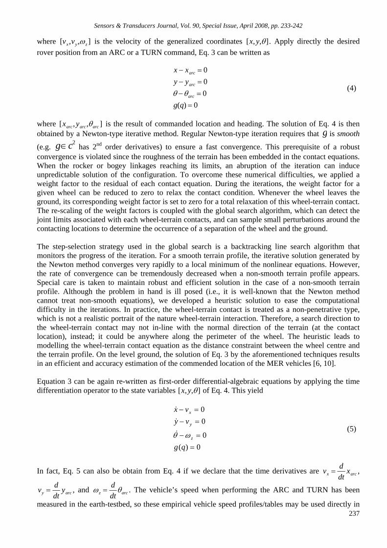
Sensors & Transducers Journal, Vol. 90, Special Issue, April 2008, pp. 233-242
237
where [vx ,vy,ωz ] is the velocity of the generalized coordinates [x, y,θ]. Apply directly the desired rover position from an ARC or a TURN command, Eq. 3 can be written as
x − xarc = 0y − yarc = 0θ −θarc = 0g(q) = 0
(4)
where [xarc, yarc,θarc ] is the result of commanded location and heading. The solution of Eq. 4 is then obtained by a Newton-type iterative method. Regular Newton-type iteration requires that g is smooth
(e.g. g∈c2 has 2nd order derivatives) to ensure a fast convergence. This prerequisite of a robust convergence is violated since the roughness of the terrain has been embedded in the contact equations. When the rocker or bogey linkages reaching its limits, an abruption of the iteration can induce unpredictable solution of the configuration. To overcome these numerical difficulties, we applied a weight factor to the residual of each contact equation. During the iterations, the weight factor for a given wheel can be reduced to zero to relax the contact condition. Whenever the wheel leaves the ground, its corresponding weight factor is set to zero for a total relaxation of this wheel-terrain contact. The re-scaling of the weight factors is coupled with the global search algorithm, which can detect the joint limits associated with each wheel-terrain contacts, and can sample small perturbations around the contacting locations to determine the occurrence of a separation of the wheel and the ground. The step-selection strategy used in the global search is a backtracking line search algorithm that monitors the progress of the iteration. For a smooth terrain profile, the iterative solution generated by the Newton method converges very rapidly to a local minimum of the nonlinear equations. However, the rate of convergence can be tremendously decreased when a non-smooth terrain profile appears. Special care is taken to maintain robust and efficient solution in the case of a non-smooth terrain profile. Although the problem in hand is ill posed (i.e., it is well-known that the Newton method cannot treat non-smooth equations), we developed a heuristic solution to ease the computational difficulty in the iterations. In practice, the wheel-terrain contact is treated as a non-penetrative type, which is not a realistic portrait of the nature wheel-terrain interaction. Therefore, a search direction to the wheel-terrain contact may not in-line with the normal direction of the terrain (at the contact location), instead; it could be anywhere along the perimeter of the wheel. The heuristic leads to modelling the wheel-terrain contact equation as the distance constraint between the wheel centre and the terrain profile. On the level ground, the solution of Eq. 3 by the aforementioned techniques results in an efficient and accuracy estimation of the commended location of the MER vehicles [6, 10]. Equation 3 can be again re-written as first-order differential-algebraic equations by applying the time differentiation operator to the state variables [x, y,θ] of Eq. 4. This yield
0)(0
00
==−
=−=−
qg
vyvx
z
y
x
ωθ&&
&
(5)
In fact, Eq. 5 can also be obtain from Eq. 4 if we declare that the time derivatives are vx =ddt
xarc ,
vy =ddt
yarc , and ωz =ddtθarc . The vehicle’s speed when performing the ARC and TURN has been
measured in the earth-testbed, so these empirical vehicle speed profiles/tables may be used directly in
Sensors & Transducers Journal, Vol. 90, Special Issue, April 2008, pp. 233-242
238
Eq. 5. A straightforward calculation leads to the “slip tables” approach that uses only the empirical data to approximate the slips. Then the modified Eq. 3 is resolved for the add-on slips. However, only these tables can represent the gross motion, and the dimension of these tables can be very large. Using the rigid-body motion, the velocity of the independent states can be obtained from a consistent wheel-ground speed. Since the onboard drive motor controller is always keeping up with a pre-defined profile, we can use the speed profile and the local terrain geometry for an approximated velocity of the independent variables. Moreover, the wheel-terrain slip can be incorporated in this approximation so that the vehicle total slip can be computed accordingly. A heuristic approach is to “average” the wheel-ground speed of each wheel for the independent velocity [vx ,vy,ωz ]. Let the i− thwheel’s velocity projected onto the plane interpolation of the terrain patch under the wheel be
viW = (I −PiPi
T )v iW , (6)
where (I −PiPi
T ) is the projection and v iW is the nominal wheel speed. Assuming the rigid contact
condition, the wheel-ground speed is along the tangential direction of the contact plane, as shown in Eq. 6. For all six wheels in contact with ground, the rover velocity is a linear combination of the wheel-ground velocity, e.g., vehicle’s velocity is within the convex hull of all the wheel velocity. Apply the partitioning operator and a weight factor to each of the driving wheels yields
(7)
where α∈ [0,1] and β ∈ [0,1]represent the weight factors, and ri is the location of the wheel in the rover’s navigation frame, si ∈ [−1,1] is the wheel-slip model parameter, and the sliding vector
( )vPPIv
T
y
x −=⎥⎦
⎤⎢⎣
⎡=
1δδ
δ , (8)
where v = 1n
(I − PiPiT )
i∑ vi
W is the nominal rover speed. Typically, the sliding vector is along the down
slope direction on a local patch of the terrain where the vehicle is treated as a point-mass on a gravitational field, representing the gravitational forces acting on the independent coordinates (x,y), respectively. Using Eqs. 5 and 7, the rover position and orientation, and the joint angles of the rockers and bogeys can be obtained. The weight factor is selected based on the local geometry, e.g., the wheel-ground angle. The magnitude of sliding vector is determined by the experimental data of the slip tables. Since the maximum tilt of the static stable configuration of the MER vehicles is 35 degrees, the weight factor and sliding factor are obtained from the results interpolated between 0 to 30 degrees.
vx = XT ( α6
(1+ si)i∑ vi
W + βδx )
vy =Y T ( α6
(1+ si)i∑ vi
W + βδy )
ωz = ΩT 1
3ri × vi
W( )i∑
Sensors & Transducers Journal, Vol. 90, Special Issue, April 2008, pp. 233-242
239
3. Results The numerical test for the rover slip model is illustrated by Figs. 2-5 using a synthetic terrain. The rover started at the origin (0, 0) of a 14-degrees slope. The testing sequence comprised of a 3-meter ARC driving downhill, then a 3-meter ARC back up to the origin, then TURN to 0 degree heading, then driving forth and back with two 3-meter ARCs. Comparing the “no slip” simulation using Eq. 4, with the simulation using Eq. 5 and 7, the slippage predicted by the simulation matches well with those of the experiments.
Fig. 2. Down Slope Driving 14% Slip.
Fig. 3. Up Slope Driving 14-16% Slip. Fig. 2 shows a 14% down-slope slip of the straight arc. The uphill straight arc illustrated in Fig. 3 shows a similar down-slope slide. In Fig. 4 and 5, the forward and back arcs driving on the side-slope also slide toward the down-slope direction at about 10 % of the traveling distance.
Fig. 4. Side Slope Driving 10% Slip.
Fig. 5. Side Slope Driving 10% Slip. The simulation results matched well with the results of the test-bed vehicle. In fact, the slip and sliding parameters of the rover slip model, e.g., α∈ [0,1] and β ∈ [0,1] in Eq. (7), are defaulted to the earth-vehicle’s performance on the test-bed ramp. When applied the slip model for the MER drives, the slip and sliding parameters can be adjusted to fit different type of surface textures. We learned during our initial drives in each terrain that driving on level ground typically leads to accurate and predictable mobility performance; e.g., Spirit only accumulated 3% position error over 2

Sensors & Transducers Journal, Vol. 90, Special Issue, April 2008, pp. 233-242
240
kilometers of driving [8]. Before driving into Endurance Crater, a series driving tests were carried out to establish a set of slip tables for MER vehicles. These tables measure the slippage percentage based on the tilt angle of the vehicle assuming a flat surface underneath. We have implemented the slip tables in RSVP simulation as the baseline method to compute the weight factors in Eq. 7. From the test results, the vehicle exhibits about 1 % slip (of the total driving distance) per degree on a slope ranging 10-20 degrees sandy surface. Similar performance on the MER vehicles when driving on the Martian surface covered with “blue berries”, that is a small grind of round pebbles. While most of the distance covered by the rovers was on level ground, most of the sols and most of the approach drive occurred on slopes. The rovers invariably slip when driving on slopes, making VisOdom essential for safe and accurate driving. To construct a successful drive on high slope areas, accurate estimation of the commanded location can only be obtained with the correct vehicle slips. On sol 1329, Opportunity drove inside the Victoria Crater approaching the science target located on layered outcrop as shown in Fig. 6 indicated by the green clover at the lower left corner. Blue lines in the pictures represent the path of the rover centre while the green lines are the track of the middle wheels, and the red lines enclosed the “keep-out zoom” where the drive will be halted if the rover centre entered.
Fig. 6. Inside Victoria Crater without (left) vs. with (right) the slip model. The planned path is 4.4 meters as shown in Fig. 6. With no slip model, the predicted path and the onboard VisOdom estimation differed by about 0.5 meters, a total slip of 10%. The predicted path using the slip model is shown in the right picture of the Fig. 6. Using α=0.23 and β = 0.81 the simulated path matches well with the actual rover motion. Note that the slope of this course is between 16 t0 19 degrees. Endurance Crater Another validation of this modeling technique is the Opportunity drive on sol 304, where the goal is to place the science targets into the rover’s robotic arm’s work volume. The rover drove 8 meters west and gained 0.9 meters in elevation using VisOdom on the slope about15-18 degrees. VisOdom maintained the on-board position knowledge during the drive, while the rover drivers planned the sequence with preempted corrections. In Fig. 7, the simulated paths with and without the slip model are compared with the on-board VisOdom estimated path. It is cleared that the slip model produces a better prediction.

Sensors & Transducers Journal, Vol. 90, Special Issue, April 2008, pp. 233-242
241
Fig. 7. Endurance Crater without Slip (left) and with 14 % Slip (right). 4. Conclusions The proposed slip model for the Mars Exploration Rovers is an effective tool to predict and validate the mobility of the rovers. Using the wheel velocity, the model, derived from a simplified vehicle dynamics, computes an accurate vehicle slippage based on the terrain geometry. To date, the slip model has been used in the daily basis to command the MER rovers driving in the Martian environment. Acknowledgements Thanks to Jeff Biesiadecki for insightful discussion on the motor controller onboard the MER flight system, RSVP team lead Brian Cooper and the team members (Frank Hartman, Scott Maxwell, and John Wright) for supporting the inclusion of the slip model in RSVP, Mark Maimone for fruitful discussion on validating the slip model using the telemetry and VisOdom data. The work described in this paper was carried out at the Jet Propulsion Laboratory, California Institute of Technology, under a contract to the National Aeronautics and Space Administration. Copyright 2008 California Institute of Technology. Government sponsorship acknowledged. References [1]. B. Cooper, F. Hartman, S. Maxwell, and J. Wright, J. Yen, Using RSVP for Analyzing State and Previous
Activities for the Mars Exploration Rovers, In SpaceOps, Montreal, Canada, 2004. [2]. Yang Cheng, Mark Maimone, and Larry Matthies, Visual odometry on the Mars Exploration Rovers,
In IEEE Conference on Systems, Man and Cybernetics, The Big Island, Hawaii, USA, October 2005. [3]. J. Yen, A. Jain and B. Balaram, ROAMS: Rover Analysis, Modeling and Simulation, In the Proc. of 5th
iSAIRAS, ESA, Netherland, 1999. [4]. E. J. Haug, Computer Aided Kinematics and Dynamics of Mechanical Systems, Allyn-Bacon, 1989. [5]. Biesiadecki J., Henriquez D., and Jain A., A Reusable, Real-Time Spacecraft Dynamics Simulator,
Proceedings of the Sixth Digital Avionics Systems Conference, Irvine, CA, October 1997. [6]. S. Maxwell, et. al, The best of both worlds: Integrating textual and visual command interfaces for mars
rover operations, in Proc. IEEE Syst., Man, Cybern. Conf., 2005, Vol. 2, pp. 1384–1388. [7]. Rongxing Li, et al. Spirit rover localization and topographic mapping at the landing site of Gusev Crater,
Mars, JGR-Planets, Special Issue on Spirit Rover, 111 (E02S06, doi: 10.1029/2005JE002483). http://www.agu.org/journals/ss/SPIRIT1/
[8]. Mishkin A. H., Limonadi D., Laubach S. L., Bass D. S., Working the Martian night shift - the MER surface operations process, Robotics & Automation Magazine, IEEE, Vol. 13, Issue 2, June 2006, pp. 46 – 53.

Sensors & Transducers Journal, Vol. 90, Special Issue, April 2008, pp. 233-242
242
[9]. Biesiadecki J. J., Leger P. C. and Maimone M. W., Tradeoffs between directed and autonomous driving on the Mars Exploration Rovers, International Journal of Robotics Research, 26, 1, 2007, pp. 91–104.
[10]. J. Yen, B. Cooper, F. Hartman, S. Maxwell and J. Wright, Sequence rehearsal and validation on surface operations of the Mars Exploration Rovers, In SpaceOps.
[11]. E. J. Haug and J. Yen, Implicit Numerical Integration of Constrained Equations of Motion via Generalized Coordinate Partitioning, ASME J. of Mechanical Design, Vol. 114, June, 1992, pp. 296-304.
[12]. J. Yen and L. R. Petzold An Efficient Newton-Type Iteration for the Numerical Solution of Highly Oscillatory Constrained Multibody Dynamic Systems, SIAM J. Sci. Stat. Comput., Vol. 19, No. 5, Sept. 1998, pp. 1513-1534.
[13]. D. M. Helmick, S. I. Roumeliotis, Y. Cheng, D. Clouse, M. Bajracharya, L. Matthies, Slip-Compensated Path Following for Planetary Exploration Rovers, Advanced Robotics, Vol. 20, No. 11, November, 2006, pp. 1257-1280.
___________________
2008 Copyright ©, International Frequency Sensor Association (IFSA). All rights reserved. (http://www.sensorsportal.com)

Sensors & Transducers Journal, Vol. 90, Special Issue, April 2008, pp. 243-254
243
SSSeeennnsssooorrrsss &&& TTTrrraaannnsssddduuuccceeerrrsss
ISSN 1726-5479© 2008 by IFSA
http://www.sensorsportal.com
Actual Excitation-Based Rotor Position Sensing in Switched Reluctance Drives
Ibrahim AL-BAHADLY
School of Engineering and Advanced Technology, Massey University Palmerston North, PN321, New Zealand
Tel.: +64 6 350 5799, fax: +64 6 350 2259 E-mail: [email protected]
Received: 15 October 2007 /Accepted: 20 February 2008 /Published: 15 April 2008 Abstract: The sensing of the rotor position for Switched Reluctance (SR) motor is necessary for excitation control so as to obtain the best performance. The rotor position for SR motor control has usually been measured using a physical rotor position transducer attached to the rotor shaft. The fitting of a rotor position transducer on an SR motor requires additional electrical connections and additional cost, it is also a potential source of unreliability. Considerable attention has recently been applied to various methods for sensorless rotor position measurement, generally based on measurement of phase current and flux and a preknowledge of the magnetic characteristics. This paper presents two methods which deduce sensorless rotor position information by monitoring the actual excitation signals of the motor phases. This is done without the injection of diagnostic current pulses and has the advantages that the measured current is large and mutual effects from other phases are negligible. Copyright © 2008 IFSA. Keywords: Rotor position sensing, Sensorless control, Switched reluctance motors 1. Introduction The structure of the switched reluctance motor is simple, robust and very reliable in operation. The machine has a salient pole stator with concentrated excitation windings and a salient pole rotor with no conductors or permanent magnets. Unlike induction motors or DC motors the SR motor cannot run directly from an AC or DC supply [1]. The flux in the SR motor is not constant, but must be established from zero every working step. A power converter circuit must supply unipolar current pulses, timed accurately to coincide with the rising inductance period of each phase winding. It is

Sensors & Transducers Journal, Vol. 90, Special Issue, April 2008, pp. 243-254
244
therefore advantageous to feed rotor position information from a shaft mounted sensor back to the control board (see Fig. 1(a)). Much has been made of the undesirability of the shaft sensor, because of the associated cost, space requirement, and possible extra source of potential failures. Operation without the shaft sensor (see Fig. 1(b)) is possible and several schemes have been reported. But to achieve the performance possible with even a simple shaft sensor, considerable extra complexity is necessary in the controller, particularly if good starting and running performance is to be achieved with a wide range of load torques and inertias. Much the same is true for the permanent magnet brushless motor and the induction motor variable speed drives.
commutation + current control
power electronicconverter
machine
positionsensor
commutation +current control
power electronicconverter
machine
positionestimation
a
b
Fig. 1. Schematic arrangement of the switched reluctance drive: (a) with position sensors, (b) with sensorless position estimator.
Much recent and current research is directed at determining rotor position from winding currents and/or voltages, either those normally occurring or from those specially injected for this purpose. The early proposed methods were to identify a position during the period for which the phase incremental inductance is rising (or falling) by measuring the current rise times with constant amplitude chopping (or vice versa). A high chopping frequency is necessary to obtain sufficient resolution at high speed. Furthermore, the mutual effect of other phase currents and the back emf at other than very low speeds are very significant and can not be neglected. So far, there is no such technique reported that has been successful in covering the entire speed range. This paper reports the development of two new methods based on using the actual motor excitation signals, not an injected signals for sensing purposes. The first method, described in section 4, is especially suited to medium and high speed operation (single pulse mode), but can be extended to low speeds. The second method, described in section 5, can cover the entire speed range, at the expense of increased computational requirement. This has been made practicable with the recent advances in digital signal processor (DSP) and their continuous decrease in cost.

Sensors & Transducers Journal, Vol. 90, Special Issue, April 2008, pp. 243-254
245
2. Sensorless Position Estimation Various methods have been proposed to eliminate the rotor position transducer, the majority of which aim to deduce rotor position by the measurement and examination of the current and flux-linkage (or inductance) in one or more phases of the motor. Comprehensive reviews of these methods have been published in [2]-[4]. The methods fall mainly into two groups. In the first group [5]-[8] test signals of different kinds are introduced during the time when a phase is normally not energized. For motoring operation this is generally during the falling inductance period or, at low speeds, around the minimum inductance periods. The test signals need to be of low amplitude to; 1) avoid negative torque production; 2) avoid back-emf effects; 3) avoid saturation effects (i.e. dependence of inductance on current in addition to rotor position) and 4) minimize the size and cost of additional injection circuitry where this is necessary. These low amplitude test signals are susceptible to mutual interference from the excitation currents in other phases and this is the main problem with these methods. At high speeds the excitation waveform occupies the majority of the phase period which, seriously restrict the injection of test signals. Thus, these methods are more suited for lower speed operation. The second group of methods [9]-[13] utilizes the excitation current waveform. Since diagnostic current pulses in a non-energized phase are of necessity small and suffer from mutual effects, it is sensible to examine the use of the main excitation current waveform for the purpose of rotor position sensing. This current already exists and does not require additional switching or injection circuitry. If at a given instant the flux-linkage ψ θ( , )i or inductance L i( , )θ is known and the current i is known, then this defines the rotor position θ provided, it is also known whether the inductance is rising or falling. The latter is generally obvious from the positioning of the excitation which will be predominantly in the rising inductance region for motoring operation. The position can be looked up in pre-stored tables of ψ or L against θ and i . These two groups cover the main-stream methods for sensorless detection of SR rotor position. However, there are a number of other proposals and published work which do not fit directly into these groups; such as the use of a state observer [14], monitoring back emf [15] and monitoring mutually induced voltages [16]. It is evident from the number of publications that research in the area of sensorless position detection is very active but that considerable further work will be required before a reliable and commercially applicable method is fully developed. 3. Rotor Position Sensing Based on Actual Excitation This section introduces two different methods of rotor position measurements for the control of switched reluctance motors without the use of optical or magnetic sensors. Both methods utilize stored magnetic characteristics for a motor phase and estimate rotor position by monitoring the excitation signals. The main advantages of these methods are: 1) the injection of additional signals into the machine windings are not needed;

Sensors & Transducers Journal, Vol. 90, Special Issue, April 2008, pp. 243-254
246
2) the position measurement is based on flux linkage / current / position data, so that saturation and back emf do not introduce errors in the position estimation; 3) the measurements take place during the rising inductance period which is the most sensitive region for rotor angle discrimination and it is not necessary to specify mechanical load parameters; 4) the rotor position estimation is less susceptible to mutual effect from other phases. One method involves a 3-dimensional lookup tables and requires continually repetitive comparison of measured and stored values. This method will be described in more detail in section 5. Whilst the other method makes one single position measurement per phase cycle and need only 2-dimensional lookup tables of magnetic data. This method is described in section 4. Both of these methods are verified experimentally. 4. Method Based on Single Measurement per Phase Cycle This method is based on estimating a particular rotor position on a phase by phase basis and measuring flux-linkage and current when this estimated position is reached. By comparing the measured flux-linkage with the stored flux-linkage corresponding to the particular (reference) position for the measured current, the angular difference between the estimated position and the reference position can be calculated. One position measurement for each phase per phase period will be made. The measurement system will therefore be a direct replacement for the existing incremental position sensor and no change need to be made to the existing control strategies. Consider the schematic phase current and voltage waveforms shown in Fig. 2.
current L( )θ
phase period voltage
θo θmθq
θ r
θ
ψ m
Fig. 2. Typical current and voltage waveforms at high speed in relation to the inductance profile. The reference angle θ r is the prechosen position for which the 2-dimensional characteristic is stored, and is preferably fixed for the entire speed range. The measurement angle θ m is the actual position at which the measurement is made - ideally, the measurement angle should coincide with the reference. The measurement angle may be situated after

Sensors & Transducers Journal, Vol. 90, Special Issue, April 2008, pp. 243-254
247
the commutation point θ q although it is preferred to be before the commutation angle as shown in the figure above. At the previous measurement angle θ m' (for the previous phase), and knowing the speed, the time to the next θ r can be calculated. When this time has elapsed the measured flux-linkage ψ m and current im are recorded. The flux-linkage is best measured by integrating from the time corresponding to θ o in Fig. 2 - i.e.: ψ
θ
θ
m V iR dto
m= −∫ ( ) , (1)
where V is the phase voltage and R is the phase resistance. The integrator for ψ m will be started at θ o when the phase is switched on. In general, due to error in the calculation or acceleration/deceleration effects, the position θ m will be different to θ r . Having obtained the measured flux-linkage and current at the unknown position θ m (but assumed to be reasonably close to the reference position), the expected value ψ e for the flux-linkage corresponding to the measurement current im and the reference angle θ r can be obtained from the look up table. This is shown in Fig. 3.
current (A)
f
0100200300400500600700800900
0 0.5 1 1.5 2 2.5 3
ψ e
im
Fig. 3. Flux-linkage v current characteristic for rotor angle θ r . Theψ e will differ from ψ m , unless θ m =θ r . For small variation, ∆θ about θ r for a particular im . ∆ψ ψ ψ( )im m e= − (2)
∆ ∆θ∂θ∂ψ
ψ= ( ) ( )m mi (3)
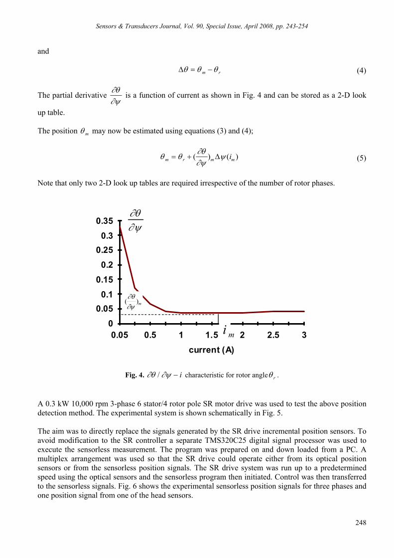
Sensors & Transducers Journal, Vol. 90, Special Issue, April 2008, pp. 243-254
248
and ∆θ θ θ= −m r (4)
The partial derivative ∂θ∂ψ
is a function of current as shown in Fig. 4 and can be stored as a 2-D look
up table. The position θ m may now be estimated using equations (3) and (4);
θ θ∂θ∂ψ
ψm r m mi= + ( ) ( )∆ (5)
Note that only two 2-D look up tables are required irrespective of the number of rotor phases.
current (A)
00.05
0.10.15
0.20.25
0.30.35
0.05 0.5 1 1.5 2 2.5 3
( )∂θ∂ψ m
i m
∂θ∂ψ
Fig. 4. ∂θ ∂ψ/ − i characteristic for rotor angleθ r . A 0.3 kW 10,000 rpm 3-phase 6 stator/4 rotor pole SR motor drive was used to test the above position detection method. The experimental system is shown schematically in Fig. 5. The aim was to directly replace the signals generated by the SR drive incremental position sensors. To avoid modification to the SR controller a separate TMS320C25 digital signal processor was used to execute the sensorless measurement. The program was prepared on and down loaded from a PC. A multiplex arrangement was used so that the SR drive could operate either from its optical position sensors or from the sensorless position signals. The SR drive system was run up to a predetermined speed using the optical sensors and the sensorless program then initiated. Control was then transferred to the sensorless signals. Fig. 6 shows the experimental sensorless position signals for three phases and one position signal from one of the head sensors.

Sensors & Transducers Journal, Vol. 90, Special Issue, April 2008, pp. 243-254
249
SRM drive
3-phaseSRM
loading system
position sensors
current transducers
ADC
TMS320 C25
PC
multiplex
voltage currents
sensorless positions
interfaceisolation
Fig. 5. Schematic diagram for the experimental test system.
Fig. 6. Experimental sensorless position signals (Voltage scale: 5 volt/div, Time scale: 1 ms/div).
The presence of the optical sensors enabled a comparison to be made between the optical position indicators and those from the sensorless method under different conditions of speed and torque. For a high resolution comparison, the maximum inductance angle has been indicated for both signals. Fig. 7 shows a typical oscilloscope waveform with the sensorless position indicators on the bottom trace, and those from the optical sensors on the top trace. The time difference between these represents the measurement error. This could be obtained by expanding the time scale on the oscilloscope or displaying a third high frequency waveform as shown in Fig. 7.

Sensors & Transducers Journal, Vol. 90, Special Issue, April 2008, pp. 243-254
250
Fig. 7. Comparison of optical and sensorless-method position indicators for one phase Top trace - sensor signal 5 volt/div; Middle trace - HF comparison signal 2 volt/div;
Bottom trace - sensorless signal 2 volt/div; Time scale - 500 microsecond/div. The SR drive was demonstrated to operate in satisfactory manner with sensorless position measurement over a significant speed range (100 to 10,000 rpm) and with different levels of load torque. The positional error was measured to be within +/-1.1 degree which did not significantly reduce the drive performance. The method however only works provided the current pulse is of sufficient duration for a measurement to be made - i.e. it does not work at very low or zero torque levels. This major deficiency which must be corrected. The aim of this method was to produce a simple algorithm such that the measurement computation may be achieved by the existing SR drive microprocessor/controller without requiring additional microprocessor or a more powerful digital signal processor. 5. Method Based on Continuous Measurements This method is based on earlier work by Acarnley et. al. [17], [18] for permanent magnet motors. The rotor position in this method is estimated continuously using a predictor/corrector routine which performs the following stages; firstly, the flux-linkage can be predicted from voltage and current measurements. Then, combine the predicted flux-linkage with predicted rotor position based on the previous measurement and using the look up stored flux linkage/current/rotor position, estimated current can be obtained. Compare estimated and measured currents to derive a current error, then translate this current error to a position error using stored machine characteristics. Finally, the predicted position can be corrected using the position error. The algorithm is illustrated schematically in Fig. 8.
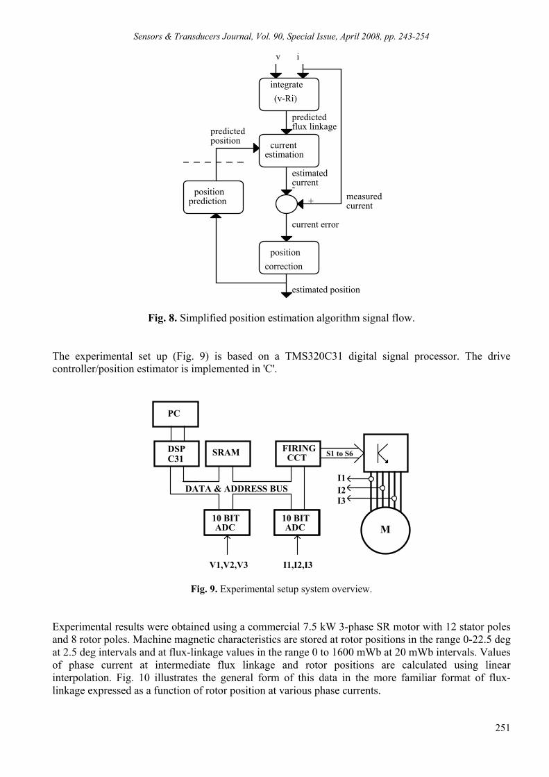
Sensors & Transducers Journal, Vol. 90, Special Issue, April 2008, pp. 243-254
251
v i
integrate (v-Ri)
predictedflux linkage
currentestimation
-+
current error
positioncorrection
positionprediction
estimated position
estimatedcurrent
measuredcurrent
predictedposition
Fig. 8. Simplified position estimation algorithm signal flow.
The experimental set up (Fig. 9) is based on a TMS320C31 digital signal processor. The drive controller/position estimator is implemented in 'C'.
FIRINGCCTSRAM
10 BITADC
10 BITADC
S1 to S6
DATA & ADDRESS BUSI1I2
M
V1,V2,V3 I1,I2,I3
PC
DSPC31
I3
Fig. 9. Experimental setup system overview. Experimental results were obtained using a commercial 7.5 kW 3-phase SR motor with 12 stator poles and 8 rotor poles. Machine magnetic characteristics are stored at rotor positions in the range 0-22.5 deg at 2.5 deg intervals and at flux-linkage values in the range 0 to 1600 mWb at 20 mWb intervals. Values of phase current at intermediate flux linkage and rotor positions are calculated using linear interpolation. Fig. 10 illustrates the general form of this data in the more familiar format of flux-linkage expressed as a function of rotor position at various phase currents.

Sensors & Transducers Journal, Vol. 90, Special Issue, April 2008, pp. 243-254
252
flux linkage (Wb)2.0
1.0
0
rotor position (degrees)0 5 10 15-5-10-15 20-20
current (A)25.0
10.0
5.0
2.01.0
Fig. 10. Flux-linkage versus rotor position at various phase current. Fig. 11 shows typical results from the position estimation algorithm when the drive is operating at a constant speed. The results have been obtained with the position being estimated in real-time and being used as a feedback signal to initiate commutation between phases.
0 250 500 time (ms)
0
15
30
45
a) position (degrees)
b) phase current (A)
0
2
4
6
8
0 250 500 time (ms)
0
0.3
0.6
0.9c) phase flux linkages (Wb)
0 250 500 time (ms)
0
15
30
45
a) position (degrees)
b) phase current (A)
0
2
4
6
8
0 40 80time (ms)
0
0.3
0.6
0.9c) phase flux linkages (Wb)
0 40 80time (ms)
0 40 80time (ms)
(a)
(b)
Fig. 11. Estimated rotor position, phase current and flux-linkage at: (a) 30 rpm, (b) 500 rpm.

Sensors & Transducers Journal, Vol. 90, Special Issue, April 2008, pp. 243-254
253
In this method, there are no limits imposed on operating speeds apart from starting up from standstill. Also, since the estimation procedure produces a continuous position signal, it is a straightforward matter to implement for variations in conduction angles with speed and load. Further testing of performance and positional accuracy needs to be carried out. In the development of this method it has been assumed that the cost of processing power will continue to fall. Therefore the emphasis has been placed on the development of a method which is flexible and applicable to wide applications and operating conditions covering the entire speed range [19] and [20], at the expense of increased computational requirement. 6. Conclusions The majority of sensorless rotor position measurement methods involve the insertion of diagnostic current signals into the phases whilst these are normally not energized. These diagnostic signal methods are limited to low speed operation. It is preferable to utilize the excitation current. Why inject diagnostic current pulses if a measurable current already exists? This also has the advantage that the measured current is large and mutual effects from other phases are negligible. The two methods discussed in this paper produce rotor position measurement utilizing the excitation signals. One method makes a single measurement each phase cycle as a direct replacement for the existing incremental position sensors. It was a simple algorithm so that the measurement computation may be achieved by the existing SR drive microprocessor/controller without requiring an additional microprocessor or a more powerful digital signal processor. This method can not cope with very low speed/low torque operation. Additional improvement is necessary to make it cover the entire speed range. The method is suitable for well defined torque/speed characteristic applications such as fan and pump operations. The other method makes continuous measurements of rotor position. It covers the entire speed range. It does however require a powerful digital signal processor to implement the extensive computational requirement. The development of such a method was based on the assumption that digital signal processor prices will continue to drop, a realistic assumption. The accuracy in both methods depends on the accuracy of characterizing and measuring the flux-linkage. To minimize the error the same method of measuring flux-linkage for characterization purposes, should be used for the measurement under operating conditions. Provided sufficient accuracy is achieved in measuring and characterizing flux-linkage, then an acceptable accuracy of position measurement for SR drive control purposes can be achieved. References [1]. C. Pollock and A. Michaelides, Switched reluctance drives: a comparative evaluation, IEE Power Eng.
Journal, Vol. 9, No. 6, 1995, pp. 257-266. [2]. W. F. Ray and I. H. Al-Bahadly, Sensorless methods for determining the rotor position of switched
reluctance motors, in Proc. European Power Electronics Conf., Brighton, UK, 1993, Vol. 6, pp. 7-13. [3]. P. W. Lee and C. Pollock, Sensorless commutation techniques for brushless permanent-magnet and
reluctance motor drives, in IEE colloquium on Variable speed drives and motion control, Nov. 1992, Digest No. 1992/194, pp. 8/1-6.

Sensors & Transducers Journal, Vol. 90, Special Issue, April 2008, pp. 243-254
254
[4]. A. Kawamura, Survey of position sensorless switched reluctance motor control, IEEE IECON’94, 1994, pp. 1595-1598.
[5]. P. P Acarnley, R. J. Hill, and C. W. Hooper, Detection of rotor position in stepping and switched motors by monitoring of current waveform, IEEE Trans on Ind. Elect. , Vol. IE 32, No. 3, 1985, pp. 215-222.
[6]. N. M. Mvungi and J. M. Stephenson, Accurate sensorless rotor position detection in an SR motor, in Proc. European Power Electronics Conf., Florence, Italy, 1991, Vol. I, pp. 390-393.
[7]. G. R. Dunlop and J. D. Marvelly, Evaluation of a self commutated switched reluctance motor, in Proc. of Electric Energy Conf., Adelaide, Australia, 1987, pp. 317-320.
[8]. W. D. Harris and J. H. Lang, A simple motion estimator for variable-reluctance motors, IEEE IAS Conf. Proc., 1988, pp. 281-286.
[9]. B. G. Hedland, A method and a device for sensorless control of a reluctance motor, International patent WO 91/02401, February 1991.
[10]. J. P. Lyons, S. R. MacMinn, and M. A. Preston, Flux/current methods for SRM rotor position information, IEEE IAS Conf. Proc., 1991, pp. 482-487.
[11]. I. H. Al-Bahadly, Rotor position sensing using normal excitation in SR drives, Proceeding of the 2nd International Conference on Sensing Technology, New Zealand, November 2007, Paper ID: ICST2007020, pp. 513-518.
[12]. W. F. Ray and I. H. Al-Bahadly, A sensorless method for determining rotor position for switched reluctance motors, 5th Power Electronics and Variable Speed Drives Conf., London, UK, 1994, IEE 399, pp. 13-17.
[13]. P. P. Acarnley, C. D. French, and I. H. Al-Bahadly, Position estimation in switched reluctance drives, in Proc. European Power Electronics Conf., Spain, 1995, Vol. 3, pp. 765-770.
[14]. A. Lumsdaine and J. H. Lang, State observers for variable reluctance motors, IEEE Trans. on Ind. Elect., 1990, Vol. 37, No. 2, pp. 133-142.
[15]. P. Piatkowski, Control circuit for a variable reluctance motor, US Patent 5180960, 1974. [16]. M. Ehsani and I. Hussain, Rotor position sensing in switched reluctance motor drives by measuring
mutually induced voltages, IEEE IAS Conf. Proc., 1992, pp. 422-429. [17]. P. P Acarnley and N. Ertugrul, Rotor position estimation in pm motors, in Proc. Int. Conf. Electrical
Machines, Manchester, UK, 1992, pp. 622-626. [18]. N. Ertugrul, P. P. Acarnley, and C. D. French, Real-time estimation of rotor position in PM motors during
transient operation, in Proc. Euro. Power Electronics Conf., Brighton, UK, 1993, Vol. 5, pp. 311-316. [19]. B. Fahimi, A. Emadi, and R. B Sepe, Four-quadrant position sensorless control in SRM drives over the
entire speed range, IEEE Tran. on Power Electronics, Vol. 20, No. 1, 2005, pp. 154-163. [20]. A. Khalil, S. Underwood, I. Hussain, H. Klode, B. Lequesne, S. Gopalakrishnan, and A. Omekanda, Four-
Quadrant Pulse Injection and Sliding-Mode-Observer-Based Sensorless Operation of a Switched Reluctance Machine Over Entire Speed Range Including Zero Speed, IEEE Trans. on Industry Applications, Vol. 43, No. 3, May 2007, pp. 714-723.
___________________ 2008 Copyright ©, International Frequency Sensor Association (IFSA). All rights reserved. (http://www.sensorsportal.com)
Sensors & Transducers Journal, Vol. 90, Special Issue, April 2008, pp. 255-266
255
SSSeeennnsssooorrrsss &&& TTTrrraaannnsssddduuuccceeerrrsss
ISSN 1726-5479© 2008 by IFSA
http://www.sensorsportal.com
A Portable Nuclear Magnetic Resonance Sensor System
1R. Dykstra, 3M. Adams, 2P. T. Callaghan, 4A. Coy, 4C. D. Eccles, 2M. W. Hunter, 1T. Southern, 1R. L. Ward
1Institute of Fundamental Sciences, Massey University, Palmerston North, New Zealand 2MacDiarmid Institute of Advanced Materials and Nanotechnology, School of Chemical and Physical
Sciences, Victoria University of Wellington, Wellington, New Zealand 3Institute for Technical Chemistry and Macromolecular Chemistry, Aachen University of Technology
RWTH, D-52056, Aachen, Germany 4Magritek Ltd, 32 Salamanca Road, Wellington, New Zealand
E-mail: [email protected]
Received: 15 October 2007 /Accepted: 20 February 2008 /Published: 15 April 2008 Abstract: Nuclear Magnetic Resonance (NMR) is a relatively complex technique and normally requires expensive equipment, however with advances in computing, electronics and permanent magnet technologies, NMR is becoming more feasible as a non-invasive tool for industry. The strength of NMR is its ability to probe at the molecular level and hence gain information about molecular structure, organization, abundance and orientation. This paper presents some of the work being undertaken in developing portable NMR systems for the non-destructive testing of materials such as polymer composites, rubber, timber and concrete. Copyright © 2008 IFSA. Keywords: Nuclear magnetic resonance, Non destructive testing, Permanent magnets 1. Introduction The Nuclear Magnetic Resonance (NMR) is one of the more recent sensing technologies and has become very popular for its ability to non-invasively probe down to the molecular level the properties of many materials and living organisms. Its greatest impact has been in the areas of chemistry and medical radiology, but now it is being applied to biochemistry, structural biology, and materials science research [1]. In the past ten years, NMR has made significant contributions to horticulture [2, 3], biotechnology, chemical engineering, petroleum science and food technology and now stands on the threshold of making an impact on environmental monitoring, building technology, and security

Sensors & Transducers Journal, Vol. 90, Special Issue, April 2008, pp. 255-266
256
technology. Traditionally NMR is performed using laboratory or clinic based superconducting magnets, but now it is moving out into industry in the form of portable permanent magnet based systems. NMR development is being driven by advancements in electronics, computing and magnet technology and so continues to advance in capability and application. 2. Nuclear Magnetic Resonance Certain nuclei possess an intrinsic angular momentum and magnetic moment and when placed in a magnetic field, B0, the nuclear moments will precess about the applied field direction at the Larmor frequency ω0 = γB0 (Fig. 1). The spins may be aligned or opposed to the field direction. At room temperature more spins are aligned than opposed with the field giving rise to a net magnetization vector, M, aligned with the applied field.
a) b)
B 0
Fig. 1. Nuclear magnetic moments a) before and b) after the application of a magnetic field. We interact with this magnetization by applying short radio frequency (RF) pulses at the Larmor frequency to a resonator surrounding the sample. The magnetic component of this pulse, B1, causes the magnetization to rotate away from the z (B0) axis into the x-y plane (Fig. 2). Once the pulse has finished the magnetization will continue to precess about B0 at ω0. The same resonator which produced the B1 pulse can now be used to detect the EMF induced by the precessing magnetization. This induced signal, called the free-induction decay or FID, has a level ranging from µV to mV and takes the form of a decaying sine wave. The decay arises from relaxation processes which cause the perturbed magnetization to return to its equilibrium position. The characteristics of the relaxation provide insight in to the molecular environment within the sample and the dynamic processes taking place.
x
y
z
M
B0b)
x
y
z
M
a)B0
B1
Fig. 2. a) During the B1 pulse the magnetization spirals down about the z axis until it ends up in the x-y plane; b) Following the B1 pulse the magnetization precesses freely in the x-y plane at frequency ω0.

Sensors & Transducers Journal, Vol. 90, Special Issue, April 2008, pp. 255-266
257
Superconducting magnets have been the key to the success of laboratory based NMR systems, however they can cost millions of dollars to purchase, are very expensive to maintain and require special facilities to house them. But the information that NMR can obtain makes them invaluable. Nuclei are affected by other surrounding nuclei which gives rise to a distribution of resonant frequencies. This property is the heart of NMR spectroscopy and allows the determination of nuclear structure. By applying additional magnetic field gradients, spatial information can also be obtained. This is the basis for Magnetic Resonance Imaging (MRI). 3. Portable NMR Systems NMR is now moving out of the laboratory and into the field in the form of low cost permanent magnet based systems [10]. They are limited in performance when compared to laboratory systems but nevertheless are still very useful tools for specific applications. Every NMR system whether laboratory based or portable basically consists of a probe, a set of supporting electronics and a user interface for controlling the system and observing/collecting the data. The block diagram for such a system is pictured in Fig. 3.
Fig. 3. NMR System Architecture.
3.1. Portable NMR Probes Probes come in a range of sizes and designs and are the critical interface between the material that one wants to study and the user. The performance of the entire system is largely dependent upon the probe. 3.1.1. The NMR “MOUSE” The Mobile Universal Surface Explorer (MOUSE) probes, developed by a group in Aachen, Germany [4] are based on the principles of “inside-out” NMR where the region of interest is external to the probe. They were initially developed for analyzing rubber and plastics, but have now been applied to areas such as the moisture determination of historic documents and buildings. The NMR-MOUSE is a surface probe that can only be used to obtain data from samples that are located within a few mm of the probe surface. Fig. 4 gives a schematic and constructed view of the hand held probe. Two

Sensors & Transducers Journal, Vol. 90, Special Issue, April 2008, pp. 255-266
258
rectangular neodymium-iron-boron permanent magnets are placed on an iron yoke to generate the necessary B0 field that is aligned with the surface of the probe. A solenoidal B1 coil is used to interact with any sample that is placed near the probe surface.
Fig. 4. Schematic of NMR-MOUSE, magnet and B1 coil configuration (left),
constructed NMR-MOUSE (right) [4]. An alternative to this design is the handheld single cylindrical bar magnet MOUSE shown in Fig. 5 [4, 9]. Here a “double D” B1 coil is placed directly on the end surface of a cylindrical magnet and is designed to generate a field parallel with the surface of the probe. This is the opposite to the configuration of the earlier two magnet MOUSE design. Again only samples within a few mm from the surface can be measured.
Fig. 5. The handheld single bar magnet MOUSE. The field strength at the surface is approximately 0.46 T, equating to a proton resonance frequency of 19 MHz. The strength of the alternating field produced
by the B1 coil for 100 W of RF power is 1.5 mT and the typical B1 pulse duration is 4 µs [4, 9]. 3.1.2. The NMR “MOLE” What is required for applications such as the monitoring of drying concrete is a probe that can obtain data from deep inside the material. A probe called the NMR-MOLE was designed to produce a one

Sensors & Transducers Journal, Vol. 90, Special Issue, April 2008, pp. 255-266
259
cubic centimeter region 10 mm into the sample (Fig. 6) [5, 8]. A series of individual magnets were used to approximate a ring magnet and a further magnet was placed in the centre. The position of central magnet and the angle and positions of the ring magnets were adjusted until the desired field profile was achieved. The probe has a diameter of 250 mm, field strength of 65 mT at the sweet-spot and weighs approximately 6 kg. The B1 coil was constructed using a printed circuit board (Fig. 7) and produces a 250 µT field in the sample region for 100 W of RF power. The typical B1 pulse duration is 30 µs.
Fig. 6. (a) The configuration of magnets used to produce a homogenous region [5, 8]. (b) The complete prototype NMR-MOLE probe. The magnets are placed into a plastic housing and the B1 coil
is placed onto the surface as shown.
Fig. 7. NMR-MOLE B1 coil, a variation of the “double D” coil design [8].
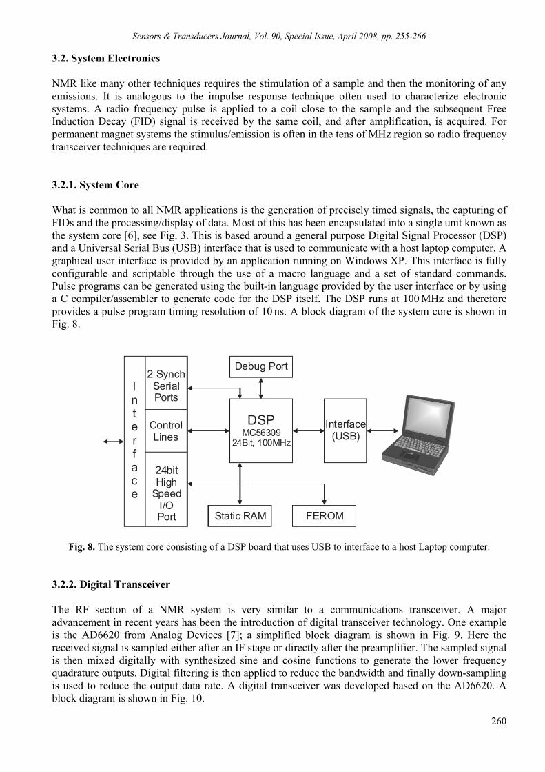
Sensors & Transducers Journal, Vol. 90, Special Issue, April 2008, pp. 255-266
260
3.2. System Electronics NMR like many other techniques requires the stimulation of a sample and then the monitoring of any emissions. It is analogous to the impulse response technique often used to characterize electronic systems. A radio frequency pulse is applied to a coil close to the sample and the subsequent Free Induction Decay (FID) signal is received by the same coil, and after amplification, is acquired. For permanent magnet systems the stimulus/emission is often in the tens of MHz region so radio frequency transceiver techniques are required. 3.2.1. System Core What is common to all NMR applications is the generation of precisely timed signals, the capturing of FIDs and the processing/display of data. Most of this has been encapsulated into a single unit known as the system core [6], see Fig. 3. This is based around a general purpose Digital Signal Processor (DSP) and a Universal Serial Bus (USB) interface that is used to communicate with a host laptop computer. A graphical user interface is provided by an application running on Windows XP. This interface is fully configurable and scriptable through the use of a macro language and a set of standard commands. Pulse programs can be generated using the built-in language provided by the user interface or by using a C compiler/assembler to generate code for the DSP itself. The DSP runs at 100 MHz and therefore provides a pulse program timing resolution of 10 ns. A block diagram of the system core is shown in Fig. 8.
DSPMC56309
24Bit, 100MHz
Interface(USB)
Static RAM FEROM
2 SynchSerialPorts
24bitHigh
SpeedI/OPort
Debug Port
Interface
ControlLines
Fig. 8. The system core consisting of a DSP board that uses USB to interface to a host Laptop computer. 3.2.2. Digital Transceiver The RF section of a NMR system is very similar to a communications transceiver. A major advancement in recent years has been the introduction of digital transceiver technology. One example is the AD6620 from Analog Devices [7]; a simplified block diagram is shown in Fig. 9. Here the received signal is sampled either after an IF stage or directly after the preamplifier. The sampled signal is then mixed digitally with synthesized sine and cosine functions to generate the lower frequency quadrature outputs. Digital filtering is then applied to reduce the bandwidth and finally down-sampling is used to reduce the output data rate. A digital transceiver was developed based on the AD6620. A block diagram is shown in Fig. 10.

Sensors & Transducers Journal, Vol. 90, Special Issue, April 2008, pp. 255-266
261
Fig. 9. The AD6620.
Fig. 10. Digital transceiver. The AD6644 14-bit ADC samples at a rate of 62.5 MHz and sends its digital values directly to the AD6620. The output of the AD6620 receiver is fed to the system core DSP for further processing and storage. An AD9852 Direct Digital Synthesizer (DDS) is also included to generate any required B1 signals. Both the synthesizer and the AD6620 NCO have phase and frequency hopping capabilities and are phase locked to each other and the DSP. The DSP/USB unit and RF transceiver are each built on standard Euro-card sized multi-layer PCBs (Fig. 11) and connect to each other via a back plane. 3.2.3. RF Electronics To complete the NMR spectrometer system a RF front end was developed (Fig. 12) consisting of a high power (100 W) broadband linear RF amplifier, a very sensitive low noise preamp and a fast transmit/receive switch. A directional coupler is used for tuning and matching the probe coil to 50 Ω, diodes D1 block any residual noise from the power amp during receive and diodes D2 together with a lumped element quarter wavelength transmission line act as a transmit/receive switch to protect the preamp during

Sensors & Transducers Journal, Vol. 90, Special Issue, April 2008, pp. 255-266
262
transmission. During transmission all the diodes conduct, therefore diodes D2 present themselves as a short circuit to the quarter wavelength transmission line which in turn appears as high impedance to the RF power source resulting in minimal power going into the very delicate preamp. Typically the transmit pulse duration ranges between 2 and 40 µs. A broadband variable gain amplifier was designed to amplify the signal from the preamplifier up to a level that is suitable for the digital receiver input.
Fig. 11. DSP (left) and digital transceiver (right) PCBs.
DirectionalCoupler
λ/4
Preamp
RF input
RF output
Reflected Power
Power Amp
D2
D1
Tuning
Matching
B coil1
Fig. 12. RF front end.

Sensors & Transducers Journal, Vol. 90, Special Issue, April 2008, pp. 255-266
263
3.2.4. Power Supply and Enclosure A switchmode power supply module was developed to enable the entire NMR system to be powered from a battery. The complete NMR spectrometer consisting of the DSP/USB unit, the digital transceiver, the variable gain amplifier, the RF front end and the power module was housed in a special compact enclosure to make the system portable and is shown in Fig. 13.
Fig. 13. Complete battery powered portable NMR system. The spectrometer part measures 310x230x55 mm and weighs 3.6 kg. The battery pack shown can provide 3 to 4 hours of operation, depending
on the RF power requirements. 3.2.4. System Testing The spectrometer was first used with a single bar magnet MOUSE and a rubber sample to verify that the system was operating correctly. The top part of Fig. 14 shows an echo signal obtained using 10 experiment averages. Some time after the first RF pulse, another RF pulse is applied to refocus the dephasing magnetization to form an echo. The amplitude of the echo is directly proportional to the number of protons in the sample. This refocusing idea can be repeated many times so that a series of echoes can be obtained and this is shown in the bottom part of Fig. 14. This is called a Carr-Purcell-Meiboom-Gill, (CPMG) sequence and is used to obtain information about relaxation processes that are occurring within the sample material. The decay can tell us about the molecular environment of the protons and therefore give us information about some of the material properties. 4. Experiments The first example for the potential use of portable NMR is shown below (Fig. 15) for a small (20 ml) gelating pectin sample, measured on the NMR-MOLE probe using a CPMG pulse sequence. As the viscosity of the gel increases with time, movement of water molecules becomes increasingly restricted leading to a reduced spin-spin (T2) relaxation time.
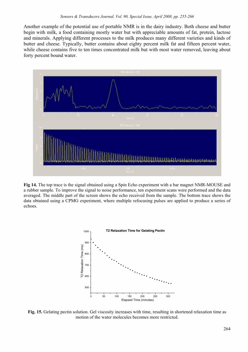
Sensors & Transducers Journal, Vol. 90, Special Issue, April 2008, pp. 255-266
264
Another example of the potential use of portable NMR is in the dairy industry. Both cheese and butter begin with milk, a food containing mostly water but with appreciable amounts of fat, protein, lactose and minerals. Applying different processes to the milk produces many different varieties and kinds of butter and cheese. Typically, butter contains about eighty percent milk fat and fifteen percent water, while cheese contains five to ten times concentrated milk but with most water removed, leaving about forty percent bound water.
Fig 14. The top trace is the signal obtained using a Spin Echo experiment with a bar magnet NMR-MOUSE and a rubber sample. To improve the signal to noise performance, ten experiment scans were performed and the data averaged. The middle part of the screen shows the echo received from the sample. The bottom trace shows the data obtained using a CPMG experiment, where multiple refocusing pulses are applied to produce a series of echoes.
0 50 100 150 200 250 300
500
600
700
800
900
1000
T2 R
elax
atio
n Ti
me
(ms)
Elapsed Time (minutes)
T2 Relaxation Time for Gelating Pectin
Fig. 15. Gelating pectin solution. Gel viscosity increases with time, resulting in shortened relaxation time as motion of the water molecules becomes more restricted.

Sensors & Transducers Journal, Vol. 90, Special Issue, April 2008, pp. 255-266
265
Figs. 16 and 17 contain measurements of T2 relaxation times using a CPMG sequence, averaged over 128 scans. In each case, the left pane shows the time-decaying echo amplitude envelope, and the right pane shows the relaxation spectrum which is an estimation of the distribution of frequencies contained in the envelope, determined using a Laplace inversion technique. Fig. 16 shows data from Rolling Meadow butter. The relaxation spectrum has three peaks; the larger centered at 29 ms with amplitude 7.4 units, the second smallest at 130 ms with amplitude 2.0 units and the smallest at 600 ms with amplitude 1.0 units. The relative amplitudes of the peaks are approximately seven-to-two-to-one. From the known properties of butter it is most likely that the seven units relates to seventy percent of the milk fat which is in crystal form, one of the smaller peaks makes up the other ten percent milk fat in globule form, and the remaining peak is the fifteen percent water.
Fig. 16. CPMG Echo attenuation data and corresponding relaxation spectrum for butter.
Fig. 17. CPMG Echo attenuation data and corresponding relaxation spectrum for cheese.
Fig. 17 shows data from Dairymaid Colby Cheese. The relaxation spectrum has two peaks; the larger centered at 21 ms with amplitude 3.3 units and the smaller at 100ms with amplitude 0.8 units. The manufacturer lists the moisture (bound water) as typically thirty seven percent by weight with fat making up the bulk of the remaining seventy three percent. The larger peak most likely corresponds to the fat and the smaller peak to the water.

Sensors & Transducers Journal, Vol. 90, Special Issue, April 2008, pp. 255-266
266
5. Conclusions A complete portable NMR system has been designed, constructed and verified and can be used with either a NMR-MOUSE or NMR-MOLE probe. Preliminary experiments verify the potential for this system to be used in the non-destructive testing of many materials. In principle, this system could be utilized in the measurement of fruit ripeness and fat content as well as other applications such as determining the molecular mobility in resins, rubbers or concrete. Acknowledgements The authors would to thank the technical staff from the science workshops of Massey University, Victoria University of Wellington and Aachen University of Technology. This project was made possible by funding provided by the New Zealand Foundation for Research Science and Technology. References [1]. Callaghan P. T., Principles of Nuclear Magnetic Resonance Microscopy, Oxford University Press, 1991. [2]. Eccles C. D., Clark C. J., Codd S. L. and Dykstra R., Construction of an MRI system for Horticultural and
Materials Science Research, Proceedings of the Fifth Electronics New Zealand Conference, 1998, pp. 45-50.
[3]. Hills B. P. and Clark C. J., Quality Assessment of Horticultural Products by NMR, Ann Report NMR Spect, 50, 2003, pp. 76-117.
[4]. Eidmann, G., Savelsberg, R., Blumler, P. and Blumich B., The NMR MOUSE, a Mobile Universal Surface Explorer, J. Magn. Reson, A 122, 1996, pp. 104-109.
[5]. NMR Apparatus, New Zealand patent application 520114 / International Patent Application No. PCT/ NZ03/00149.
[6]. Dykstra, R., A DSP/USB platform for instrumentation and control, Proceedings of the Ninth Electronics New Zealand Conference, 2002, pp. 6-11.
[7]. Analog Devices, Corporate Headquarters, One Technology Way, P. O. Box 9106, Norwood, MA 02062-9106, (http://www.analog.com).
[8]. B. Manz, A. Coy, R. Dykstra, C. D. Eccles, M. W. Hunter, B. J. Parkinson and P. T. Callaghan, A mobile one-sided NMR sensor with a homogeneous magnetic field: The NMR-MOLE, J. Magn. Reson, 183, 2006, pp. 25-31.
[9]. B. Blumich, V. Anferov, S. Anferova, M. Klein, R. Fechete, M. Adams, F. Casanova, Simple NMR-mouse with a bar magnet, Conc. Mag. Resonance B, Magn. Reson. Eng., 14, 4, 2002, 255-261.
[10]. R. Dykstra, M. Adams, P. T. Callaghan, C. D. Eccles, M. W. Hunter, T. Southern, R. L. Ward, The development of Portable NMR Systems, Proceedings of the International Conference on Sensing Technology, Palmerston North, New Zealand, 2007.
___________________
2008 Copyright ©, International Frequency Sensor Association (IFSA). All rights reserved. (http://www.sensorsportal.com)

Sensors & Transducers Journal, Vol. 90, Special Issue, April 2008, pp. 267-275
267
SSSeeennnsssooorrrsss &&& TTTrrraaannnsssddduuuccceeerrrsss
ISSN 1726-5479© 2008 by IFSA
http://www.sensorsportal.com
A Special Vibration Gyroscope
Wang Hong-Wei, Chee Chen-Jie, Teng Gong-Qing, Jiang Shi-Yu School of Science, Beijing Information Science and Technology University
Beijing, China E-mail: [email protected]
Received: 15 October 2007 /Accepted: 20 February 2008 /Published: 15 April 2008 Abstract: A novel silicon micro-machined gyroscope which is driven by the rotating carrier’s angular velocity is introduced. The principle of structure is analyzed. The mathematic module is also established. Process of making the vibration silicon modules is given and the manufacturing of “Sandwiches” sensor is showed. The gyroscope has been tested, the result have certificated that the principle of the gyroscope is correct. Copyright © 2008 IFSA. Keywords: Vibration, Gyroscope
1.Introduction In 1990’s, all kinds of micro-machined gyroscope appeared along with the development of microelectronic technology. There is two parts in those gyroscope’ sensor, one part is driving (including driving circuit), the other part is sensing (including sensing circuit). Those gyroscopes can sense Coriolis force when vibrating mass is driven by the carrier. Designing and manufacturing this kind of gyroscope is very difficult because of the micro-machined gyroscope must be driven first [1-2]. The high frequency vibrating micro-structure is the driving part. In order to avert the difficulty of the design and manufacture silicon micro-machined gyroscope’s driven part, the authors are propose to utilize rotating of the carrier itself as the driven force [3], thus the driving part needless to be used in the gyroscope. So while the carrier spin, the carrier’s yaw angular velocity or pitching angular velocity uprightness to the carrier’s spin angular velocity orientation can be detected. This structure of the gyroscope is simple, and it is easy to process.
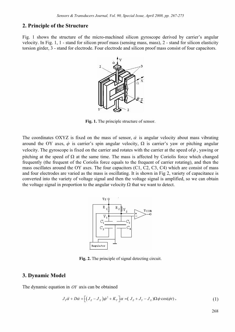
Sensors & Transducers Journal, Vol. 90, Special Issue, April 2008, pp. 267-275
268
2. Principle of the Structure Fig. 1 shows the structure of the micro-machined silicon gyroscope derived by carrier’s angular velocity. In Fig. 1, 1 - stand for silicon proof mass (sensing mass, mass), 2 - stand for silicon elasticity torsion girder, 3 - stand for electrode. Four electrode and silicon proof mass consist of four capacitors.
Fig. 1. The principle structure of sensor.
The coordinates OXYZ is fixed on the mass of sensor, α& is angular velocity about mass vibrating around the OY axes, ϕ& is carrier’s spin angular velocity, Ω is carrier’s yaw or pitching angular velocity. The gyroscope is fixed on the carrier and rotates with the carrier at the speed ofϕ& , yawing or pitching at the speed of Ω at the same time. The mass is affected by Coriolis force which changed frequently (the frequent of the Coriolis force equals to the frequent of carrier rotating), and then the mass oscillates around the OY axes. The four capacitors (C1, C2, C3, C4) which are consist of mass and four electrodes are varied as the mass is oscillating. It is shown in Fig 2, variety of capacitance is converted into the variety of voltage signal and then the voltage signal is amplified, so we can obtain the voltage signal in proportion to the angular velocity Ω that we want to detect.
Fig. 2. The principle of signal detecting circuit. 3. Dynamic Model The dynamic equation in OY axis can be obtained ( ) 2 ) cos( )Y Z X T Z Y XJ D J J K J J J tα α ϕ α ϕ ϕ⎡ ⎤+ + − + = + − Ω⎣ ⎦&& & & & &( , (1)

Sensors & Transducers Journal, Vol. 90, Special Issue, April 2008, pp. 267-275
269
where , ,X Y ZJ J J are the moments of inertia for the gyroscope mass in X, Y, Z axises; TK is the coefficient of torsion rigidity; D is the damping coefficient. Stable solution for equation (1) is ( )
( )[ ] ( )( )βϕ
ϕϕ
ϕα −
++−−
Ω−+= t
DKJJJ
JJJ
TYXZ
XYZ &&&
&cos
222
(2)
Amplitude of angular vibration is
22 2
( )
( ) ( )Z Y X
m
Z X Y T
J J J
J J J K D
ϕαϕ ϕ
+ −= Ω
⎡ ⎤− − + +⎣ ⎦
&
& &
(3)
4. Dynamic Parameter Analysis and Calculation 4.1. Rigidity Coefficient of Elastic Girder The structure of elastic girder is shown in Fig. 3, length, width and thickness of girder are L, W, and t. In order to be convenient for get the torsion rigidity coefficient of elastic girder, it can be supposed as follow: (1) Turning angular is direct proportion to girder length; (2) Warp of all brace girder ‘s cross-section are equal; (3) Twist moments of girder’s ends are equate and their orientation are contrary.
Fig. 3. Structure of supporting girder. According these assumptions, from elasticity mechanics, the total rigidity of two girders is got 3
41,3,5,......
3
1 20.657 (1 tanh )2
23
Tn
Gt w t n wKL n n w t
Gt wL
ππ
∞
=
= × −
≈ ⋅
∑ (4)
Put w=0.8 mm, L=0.8 mm, t=0.025 mm, G=5.1×10¹⁰ (N/m2) into the formulation (4), get:
TK =5.313×10⁻⁴N·m.

Sensors & Transducers Journal, Vol. 90, Special Issue, April 2008, pp. 267-275
270
4.2. Angular Vibration Damping Coefficient of Vibration Devices When a rectangle plane with length A and width B moves towards underside whose gap breadth is H, the press membrane damping coefficient is 3
3 5 51.3.5...
33 4
192 11 tanh2
96 21 tanh. 2
damp
n
F AB B n Af dh h A n BdtB AB A
h A B
µ ππ
µ ππ π
=
⎡ ⎤= = −⎢ ⎥⎣ ⎦
× ⎡ ⎤⎛ ⎞≈ − ⋅ ⋅⎜ ⎟⎢ ⎥⎝ ⎠⎣ ⎦
∑ (5)
As the structure of the vibrating mass is complex, it is difficult to calculate the damping coefficient. For reducing the calculation difficulty, the gyroscope mass is divided into three areas with distinct colors, shown in Fig 4. then add damping of three district as the gyroscope vibration global damping approximately.
Fig. 4. Damping partition. Angular vibration damping factor of three distinct are got. Three relationship curves about damping coefficient and vibration angular are shown in Fig. 5.
Fig. 5. Relationship of damping coefficient. From Fig. 5, When d=0.020 mm, we get damping coefficient 5 5(2 10 ,0) 1.231 10 ( )D N m s− −× = × ⋅ ⋅

Sensors & Transducers Journal, Vol. 90, Special Issue, April 2008, pp. 267-275
271
4.3. Relationship Curve about Gyroscope Mass Angular Vibration Inherent Frequent, Angular Vibration Amplitude and Detecting Angular Velocity
The gyroscope mass angular vibration inherent frequent calculated using dynamic parameter is
917Ts
Y
KJ
ω = = (rad/s) = 146 Hz (6)
Put the dynamic parameter into formulation (3), get relationship curve about ma vs. detecting angular velocityΩ . It is shown in Fig. 6.
Fig. 6. Curve of relationship about angle vibration range mα and angle velocity Ω. When ϕ& =17 Hz, Ω =0.01 (rad/s), 79.505 10mα
−= × (rad) and vibration amplitude of gyroscope vibration mass’ outer fringe is -93 5.03756 10 ( )
2m ma
A mα= ⋅ = ×
5. Signal Detection The signal detection circuit of micro-machined gyroscope is shown in Fig. 3. When gyroscope spin with angular rateϕ& , deflection angular α variation leads to four capacitors C1, C2, C3, C4 changing. The capacitance variety convert into voltage signal and the signal is amplified; get the signal whose amplitude correspond to detected angular velocity Ω . The capacitance variety of micro-machined gyroscope is very small and be affected by distribution capacitance easily. Signal processing use alternating current bridge, sense capacitance device is used as operation arms of the bridge. The bridge supply is equivalency amplitude high frequent alternating voltage. When operation capacitors are changed, the amplitude modulation wave signal modulated by operation capacitors variety at the output of the bridge and signal is amplified and demodulated, then get low frequent output signal. It is known in Fig. 2, as silicon pendulum without turning (α = 0), C1 = C2 = C3 = C4 = C0 and then
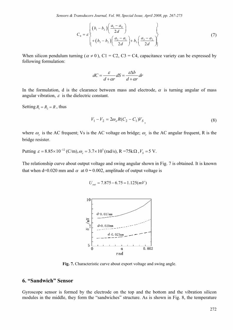
Sensors & Transducers Journal, Vol. 90, Special Issue, April 2008, pp. 267-275
272
( )
( )
1 01 2
03 22 1
3 2 3
2
2 2
a ab bd
Ca aa ab b b
d d
ε
⎧ − ⎫⎛ ⎞− ⎜ ⎟⎪ ⎪⎪ ⎝ ⎠ ⎪= ⎨ ⎬−− ⎛ ⎞⎛ ⎞⎪ ⎪+ − +⎜ ⎟ ⎜ ⎟⎪ ⎪⎝ ⎠ ⎝ ⎠⎩ ⎭
(7)
When silicon pendulum turning ( 0α ≠ ), C1 = C2, C3 = C4, capacitance variety can be expressed by following formulation: dr
rdbdS
rddC
αε
αε
+∆
=+
=
In the formulation, d is the clearance between mass and electrode, α is turning angular of mass angular vibration, ε is the dielectric constant. Setting 1 2R R R= = , thus Se VCCRVV )(2 1221 −=− ω , (8) where eω is the AC frequent; Vs is the AC voltage on bridge; eω is the AC angular frequent, R is the bridge resister. Putting 128.85 10ε −= × (C/m), 53.7 10eω = × (rad/s), R =75kΩ , SV =5 V. The relationship curve about output voltage and swing angular shown in Fig. 7 is obtained. It is known that when d=0.020 mm and α at 0~0.002, amplitude of output voltage is 7.875 6.75 1.125( )outU mV= − =
Fig. 7. Characteristic curve about export voltage and swing angle. 6. “Sandwich” Sensor Gyroscope sensor is formed by the electrode on the top and the bottom and the vibration silicon modules in the middle, they form the “sandwiches” structure. As is shown in Fig. 8, the temperature

Sensors & Transducers Journal, Vol. 90, Special Issue, April 2008, pp. 267-275
273
expansion coefficient of silicon is 6106.2 −× / .To ensure the stability of the "sandwich" structure, the temperature coefficient of expansion of the electrode has been closed with the temperature coefficient of expansion of the silicon. We choose the No.75 ceramic Substrate. Vibration silicon modules is shown in Fig. 9, the silicon quality is in the middle, outside are the frames, two flexible beams put the quality and the frames together. So that the quality can rotate around the axis consisted of two beams, the thickness of the frames are 30 um thicker than the thickness of the quality, so the two facets of the frame are 15 um higher than the two facets of the quality. The thickness of the beam is 48 um. There is prescribe hole in the center of mass of silicon, and 7 grooves outside, they are used to reduce the damping, the whole vibration modules is one structure through the micro-machined processing used the silicon as the material, Fig. 10 is the chart of the plates, blotted out regional in the map is copper electrode, electrode substrate are made by ceramics, the electrode on the top and the bottom and the vibration silicon modules in the middle formed the “sandwiches” sensor, Fig. 11 is the plate with copper electrode.
Fig. 8. “Sandwiches” sensor.
Fig. 9. Vibration silicon modules.
Fig. 10. Chart of the plates.
Fig. 11. Plate with copper electrode. 7. Process of the Vibration Silicon Modules Using the 4-inch silicon, type N, double Polishing, (100) crystal face. In the experiment, we use 30 % of the concentration of KOH solution for corrosion, temperature is 104 °C, corrosion rate is approximately 4.3. The process is shown in Fig. 12. a. 2000 Å silicon dioxide layer double growth; b. Double lithography, get rid of the oxide layer; c. 15um silicon surface of the deep corrosion each plane; d. 1.5um silicon dioxide layer double growth; e. Second double-lithography, 24 um silicon surface of the deep corrosion each plane; f. Third double-lithography, 80 um silicon surface ;

Sensors & Transducers Journal, Vol. 90, Special Issue, April 2008, pp. 267-275
274
g. of the deep corrosion each plane; h. Forth double-lithography, 64 um silicon surfaces of the deep corrosion each plane, Link up. After seven steps above, we got the vibration silicon modules, But then the silicon beam vibration unit has not been processed out, next, the process is to make the elastic beam of the silicon modules vibration. We put single silicon modules in solution for lithography silicon corrosion, then we got the vibration silicon modules, as is shown in Fig. 13.
Fig. 12. Process of silicon modules.
Fig. 13. Silicon modules. 8. Silicon Micro-machined Gyroscope Tests Gyroscope has been tested. The tests were held on dynamic stand controlled by personal computer. The Gyroscope was set in the range 5~25 Hz by a rotation simulator. The tested sensors proved the total efficiency on all the conditions of the carried tests. Dependence of the sensor output signal on the measured angular rate at different rotation frequencies of simulator is shown in Table 1 and Fig. 14.

Sensors & Transducers Journal, Vol. 90, Special Issue, April 2008, pp. 267-275
275
Table 1. Gyroscope Dependence of the sensor output signal on the measured angular rate at different rotation frequencies of simulator.
Fig. 14. Dependence sensor output signal from input rate. 9. Conclusion Depend on carrier’s rotating angular velocity as driving force without driving circuit and driving girder, the principle of this micro-machined gyroscope is correct. Because of the instability of the angular velocity of the rotating carrier itself, the output voltage error reached to 30 %.under low damp situation output signals of silicon micro-machined gyroscope is proportional to the rotate speed of the carrier. References [1]. K. Maenaka, T. Shiozawa, A study of silicon angular rate sensors using anisotropic etching technology,
Sensors and Actuators A, 1994, 43, pp. 72-77. [2]. K. Maenaka, T. Fujita, Y. Konishi, M. Maeda, Analysis of a highly sensitive silicon gyroscope With
cantilever beam as Vibrating mass, Sensors and Actuators, 54, 1996, pp. 568-573. [3]. Wang Hong-Wei, CHEE Chen-Jie, Teng Gong-Qing, Jiang Shi-Yu, A special Silicon Micro-machined
vibration Gyroscope, 2nd International Conference on Sensing Technology, November 26-28, 2007, Palmerston North, New Zealand, 2007.
___________________
2008 Copyright ©, International Frequency Sensor Association (IFSA). All rights reserved. (http://www.sensorsportal.com)
50 100 150 200 250 300 Ω/о/s ϕ& /Hz CW CCW CW CCW CW CCW CW CCW CW CCW CW CCW
5 726.8 698.4 1440 1412 2157.6 2139.4 2875.2 2845.2 3600 3568.6 4327.2 4294.211 1481.2 1449.4 2957.6 2928.8 4440.8 4417.6 5872.8 5849.8 7263 7254 8652.8 8662.417 1835.8 1803.6 3633.6 3582.2 5429.8 5324.8 7193.4 7038.8 8982.4 8772.2 10833.8 10601.225 2019 1870.6 3823.6 3677.8 5569.6 5482 7371.4 7248.8 9217.2 9139.6 11264.4 11170.2
Stability/% ±32.65 ±31.98 ±31.61 ±31.25 ±31.04 ±30.74 ±30.89 ±30.59 ±30.92 ±30.67 ±31.35 ±31.08
Sensors & Transducers Journal, Vol. 90, Special Issue, April 2008, pp. 276-283
276
SSSeeennnsssooorrrsss &&& TTTrrraaannnsssddduuuccceeerrrsss
ISSN 1726-5479© 2008 by IFSA
http://www.sensorsportal.com
An Improved CMOS Sensor Circuit Using Parasitic Bipolar Junction Transistors for Monitoring the Freshness
of Perishables
S. M. Rezaul HASAN and Siti Noorjannah IBRAHIM Center for Research in Analog and VLSI Microsystem dEsign (CRAVE),
Massey University, Auckland 1311, New Zealand E-mail: [email protected], [email protected]
Received: 15 October 2007 /Accepted: 20 February 2008 /Published: 15 April 2008 Abstract: This paper presents an improved integrated circuit sensor for emulating and monitoring the quality of perishable goods based on the surrounding temperature. The sensor is attached to the container of fresh or preserved farm or marine produce and passes on the monitored quality information from manufacturer/producer to the consumers. The sensor essentially emulates the thermal deterioration caused by the environment on its way from producer to consumer and provides a readout indicating the freshness of the goods. Compared to previous designs, parasitic substrate PNP devices in standard CMOS process instead of subthreshold MOS devices are used for emulating the activation energy of degradation (spoiling) chemical reactions. The reliability of the sensor is thus considerably enhanced compared to previous design. In addition, an analog squaring circuit is used for emulating the degradation for large activation energy thereby removing the need for a multiplier in the digital processing section and hence reducing silicon area. Simulations were carried out using a 0.18 µm TSMC CMOS process technology. The power consumed by the sensor was around 16 mW. Copyright © 2008 IFSA. Keywords: Food sensor, CMOS sensor, Parasitic bipolar devices, Freshness, Analog integrated circuits. 1. Introduction Monitoring the degradation of perishables during distribution from producer to consumer is an essential procedure in assuring acceptable quality of most farm/marine food products. On the other hand, producers have no prior knowledge of the conditions of distribution. As the perishables/goods

Sensors & Transducers Journal, Vol. 90, Special Issue, April 2008, pp. 276-283
277
may be distributed under suitable or unsuitable environmental conditions, the producers are forced to set conservative expiration dates of the products. As a result, considerable amount of perishables are often thrown away (wasted) since the expiration date has already passed, although the goods are still edible. Hence, accurate monitoring of the degradation of perishables can help in food conservation. This monitoring can be carried out by electronically emulating the thermally initiated chemical reaction that causes the degradation of the perishables. Such an emulation sensor would be attached to the perishables and carried along during the goods distribution process. It is thus subjected to the same environmental variations for the perishables and emulates the degradation of the perishables caused by the surrounding environment. By reading the calibrated output of the sensor the consumer can accurately ascertain the amount of freshness remaining in the perishable. In previous work [1], [2] sub-threshold devices are used for emulating the activation energy of chemical reactions and a digital multiplier is used to improve the dynamic range to account for high activation energy (0.4 eV-0.5 eV) [4] of most spoiling bio-chemical reactions. In this work, parasitic bipolar PNP devices are used for emulating the activation energy, thereby, considerably enhancing the reliability of the sensor. Also, an analog squaring circuit is used to increase the dynamic range of the sensor to account for large activation energy of most degradation chemical reactions in spoilage. Higher reliability can thus be achieved using this design at the cost of higher power dissipation. Preliminary work on this proposed sensor circuit was reported in [9]. 2. Emulation of the Degradation Process Using Parasitic PNP Devices as Thermosensor The degradation of perishables is a bio-chemical reaction between concentrations of two constituents; one of which is the perishable good (say, A) and the other is usually air/oxygen (say, B). The concentration of the resulting spoiling substance (say, C) is usually given by [1], [2],
[ ] [ ] [ ] ∫⎟⎟⎠
⎞⎜⎜⎝
⎛−
=1
0000t Tk
E
dtekBAC B
a
, (1)
where, [ ]0A and [ ]0B are initial concentrations of A and B and [ ]C corresponds to the concentration of the spoiling substance [10]. Ea is the activation energy for the chemical reaction, k0 is a constant of proportionality, kB is the Boltzmann constant and T is the temperature of the surrounding environment in °K. For the same activation energy, higher temperature results in a larger temporal integration with the consequence of larger concentration of spoiling substance and reduced freshness of the food products. In order to emulate the deterioration of the freshness of the perishables, use of the parasitic lateral PNP transistor of a standard CMOS (Complementary Metal Oxide Semiconductor) process (as a thermo-sensor) as shown in Fig. 1, is proposed in this paper instead of the sub-threshold NMOS device in [1], [2]. The collector current of this parasitic PNP device IC is given by,
TKqv
SC B
EB
eII η= , (2)
where IS and η are process dependent parameters [5]; vEB is the emitter-base voltage; q is the elementary charge. To set the activation energy for emulating a degradation process, two PNP transistor (PNP1 and PNP2) of similar geometry (same fixed emitter area) are biased by two different dc base voltages vb1 and vb2 (applied by external user control), and, the ratio of their collector currents is taken. Then this ratio is given by,
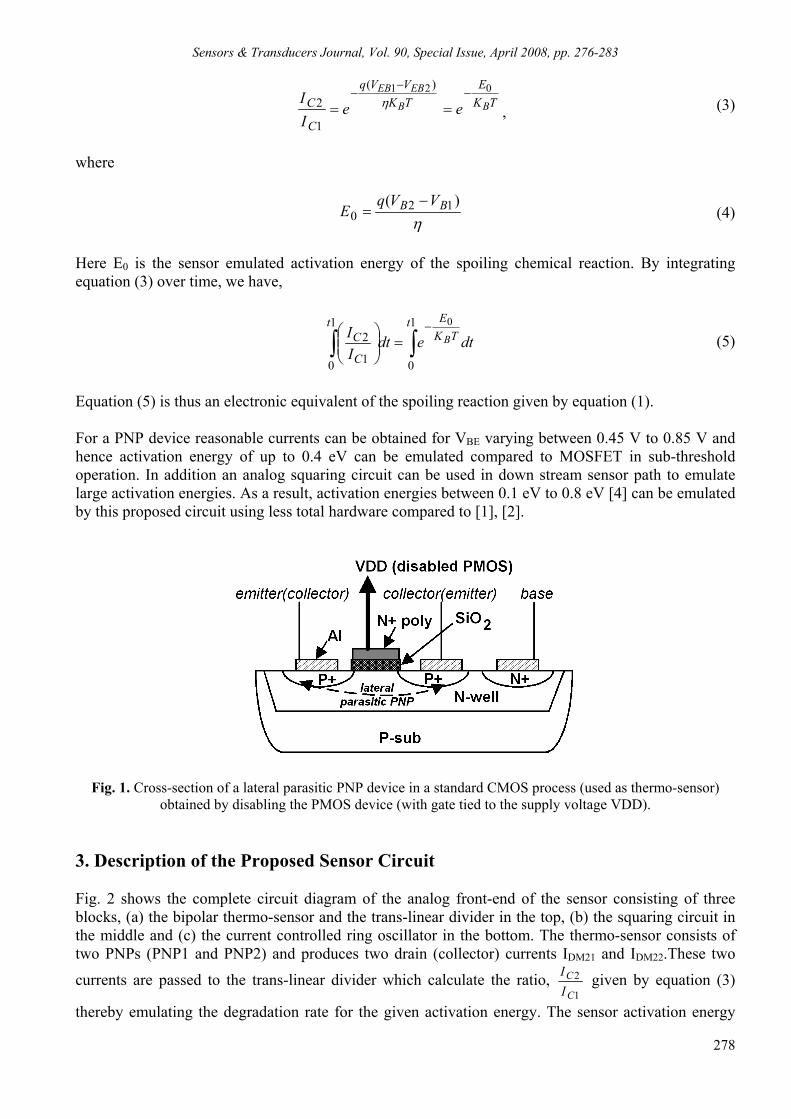
Sensors & Transducers Journal, Vol. 90, Special Issue, April 2008, pp. 276-283
278
TK
ETKVVq
C
C BB
EBEB
eeII
021 )(
1
2−
−−
== η , (3)
where
η)( 12
0BB VVq
E−
= (4)
Here E0 is the sensor emulated activation energy of the spoiling chemical reaction. By integrating equation (3) over time, we have,
∫∫−
=⎟⎟⎠
⎞⎜⎜⎝
⎛1
0
1
0 1
20tTK
Et
C
C dtedtII B (5)
Equation (5) is thus an electronic equivalent of the spoiling reaction given by equation (1). For a PNP device reasonable currents can be obtained for VBE varying between 0.45 V to 0.85 V and hence activation energy of up to 0.4 eV can be emulated compared to MOSFET in sub-threshold operation. In addition an analog squaring circuit can be used in down stream sensor path to emulate large activation energies. As a result, activation energies between 0.1 eV to 0.8 eV [4] can be emulated by this proposed circuit using less total hardware compared to [1], [2].
Fig. 1. Cross-section of a lateral parasitic PNP device in a standard CMOS process (used as thermo-sensor) obtained by disabling the PMOS device (with gate tied to the supply voltage VDD).
3. Description of the Proposed Sensor Circuit Fig. 2 shows the complete circuit diagram of the analog front-end of the sensor consisting of three blocks, (a) the bipolar thermo-sensor and the trans-linear divider in the top, (b) the squaring circuit in the middle and (c) the current controlled ring oscillator in the bottom. The thermo-sensor consists of two PNPs (PNP1 and PNP2) and produces two drain (collector) currents IDM21 and IDM22.These two
currents are passed to the trans-linear divider which calculate the ratio, 1
2
C
CII given by equation (3)
thereby emulating the degradation rate for the given activation energy. The sensor activation energy

Sensors & Transducers Journal, Vol. 90, Special Issue, April 2008, pp. 276-283
279
can be varied for different category of perishables by changing the bias voltages at the two thermo-sensor PNP bases which can be implemented by external control. The output of the trans-linear divider is feed into the squaring circuit using the current mirror consisting of the devices M14, M15, M16, M25 and M26. The squaring circuit then doubles the activation energy to account for slowly degrading perishables. Next, the current controlled oscillator is biased by the output current of the squaring circuit using the current mirror formed by the devices M35, M36, M37, M38, M39, M40, M41, M42, M53, M54, M55, M56 and M57. The ring oscillator produces oscillation pulses with frequency, f proportional to this current. The PMOS devices in the oscillator are made twice the width of the NMOS devices in order to compensate for the slower hole mobility, so that, the rise-time and fall-time of the oscillation pulses are nearly equal.
Fig. 2. Circuit diagram of the analog front-end of the quality sensor consisting of forward-active PNP thermo-sensor, strong inversion trans-linear divider circuit, squaring circuit and current controlled
5-stage ring oscillator.

Sensors & Transducers Journal, Vol. 90, Special Issue, April 2008, pp. 276-283
280
Fig. 3 shows the digital backend of the sensor. It essentially consists of a temporally resetable up-counter, a count register, an accumulator and a control circuit. The accumulator consists of an adder and feed-back register. The registers are built using Delay-Flip-Flops (D-FFs), the counters are designed using Set-Reset Toggle-Flip-Flops (T-FFs) and the Adder is designed using 8 4-bit carry-look-ahead full-adder stages. The digital up-counter counts the number of pulses for fixed short periods of time ∆t, which is proportional to the frequency f of the ring oscillator. A higher count indicates higher temperature and higher degradation of the perishables. These counts over the short periods ∆t are next accumulated by the adder-accumulator block. The total count in this accumulator output indicates how much freshness has been lost from the perishable goods. Consequently, exposure to higher temperatures during a given period of transportation and distribution of the perishables before consumption by end customer, hastens (brings closer) the expiration date.
Fig. 3. Digital back-end of the quality emulating sensor consisting of counter, input register, accumulator (adder and output register) and a control input.
The CMOS trans-linear divider [6], [7], [8] (using a reference current of 40 µA) works in the saturation QTL [8] (Quadratic trans-linear) region. The gate-to-source voltages of the MOSFETs (M27, M28, M29 and M30) in Fig. 2 form a closed loop. Then based on the trans-linear principle [6], [7], [8] the output current of the trans-linear circuit is given by,
TKE
REFC
CREFTRDIVOUT B
o
eIIIII
−∗==
1
2_ (6)
Next, the bias current for the ring oscillator, produced by the analog current squarer [3], is given by,
TKE
REFSQROUT B
o
eII2
2_
−∗=
(7)
As illustrated in Fig. 2, the current controlled oscillator is a five stage ring oscillator, whose frequency of oscillation [1] is given by,

Sensors & Transducers Journal, Vol. 90, Special Issue, April 2008, pp. 276-283
281
TK
E
L
REF
L
SQROUT B
o
eVddmC
IVddmC
If
22_
22
−== , (8)
where, m is 5 in this case for the 5-stage ring oscillator, CL is the load at the output of each inverter, with Vdd being the supply voltage. The output of the up-counter during every ∆t period is given by,
∫∫∆+ −∆+
=tt
t
TKE
L
REFtt
t
dteVddmC
Ifdt B
o22
2 (9)
And, finally the accumulated content at time t1 is given by,
∫−
=1
0
22
2_
tTK
E
L
REF dteVddmC
Ioutputfinal B
o
(10)
When this final output in the accumulator exceeds certain threshold value which has been set up in advance, the product is considered to have expired. 4. Simulation Results In order to verify the operation of the proposed freshness emulator, extensive simulations were carried out using the 6M1P 0.18 µm TSMC (Taiwan Semiconductor Manufacturing Corporation) CMOS process technology parameters. The Tanner T-SPICE v.12 circuit-level simulation software was used for this purpose. A 3 V supply voltage was used for the design. Bias voltages of 2.2 V and 2.4 V are applied to the base of NPN1 and NPN2 respectively corresponding to a base activation energy of 0.2 eV. With the squaring circuit this corresponds to an equivalent of activation energy of 0.4 eV. Fig. 4 shows the output current of the trans-linear divider for temperatures of -50 °C, -30 °C, -10 °C, 0 °C, 20 °C, 30 °C, 40 °C, 50 °C and 70 °C respectively varying between 0.7 mA to 1.7 mA. These currents are squared by the squaring circuit and mirrored to the ring oscillator for bias current control for all the 5 stages. The relationship between temperature and the output current is somewhat non-linear in accordance with equations (6) and (7), and, as can be seen from the plot in Fig. 4. However, the monotonic relationship between temperature and bias current ensures the validity of the sensory emulation proposed by this circuit. Next, Fig. 5 shows the time-period of oscillations for three different temperatures, being 6.36 ns at 70 °C, 6.9 ns at 50 °C and 7.3 ns at 40 °C. The time-period of oscillation is proportional to the rise-time and fall-time of the oscillation pulses. Higher sourcing and sinking currents provided by the bias control of the oscillator stages at higher temperatures results in shorter time-periods. So, for the same time interval ∆t (e.g. 0.1 s) the counter will provide a count of 15723270 pulses at 70 °C, 14492753 pulses at 50 °C and 13698630 pulses at 40 °C. A 32-bit up-counter is thus used in Fig. 3 for counting the pulses during a short period of 0.1 sec. Count accumulated by the adder-accumulator would be considerably higher for exposure to long periods of higher temperatures during transport and distribution, compared to exposure to lower temperatures. When the contents of the accumulator are compared with a preset count the expiry status is determined for the product/perishables. The power dissipated by the sensor was mostly due to the dc bias currents in the analog front-end circuit. The digital back-end block being designed using static CMOS logic gates only dissipates power during

Sensors & Transducers Journal, Vol. 90, Special Issue, April 2008, pp. 276-283
282
logic transition (dynamic power dissipation), and, its static power dissipation is almost zero. The sensor circuit was found to have an overall dc power drain of around 16 mW.
Fig. 4. Output currents of the trans-linear divider for temperatures of -50 °C, -30 °C, -10 °C, 0 °C, 20 °C, 30 °C,
40 °C, 50 °C and 70 °C respectively.
Fig. 5. Oscillator waveforms for the current controlled ring oscillator showing time periods of 6.36 ns, 6.9 ns and 7.3 ns respectively for temperatures of 70 °C, 50 °C and 40 °C respectively.

Sensors & Transducers Journal, Vol. 90, Special Issue, April 2008, pp. 276-283
283
5. Conclusion An emulating sensor for monitoring the quality of perishables, using MOSFET devices in the strong inversion region of operation along with parasitic PNP thermo-sensors is proposed. The circuit is implemented using a standard low-cost CMOS process technology. The circuit provides higher dynamic range in terms of activation energy from 0.1 V to 0.8 V using the PNP thermo-sensors and CMOS squaring circuit. Furthermore, the design requires less hardware than the circuit proposed by [1], [2]. Simulations indicate that the topology is quite sound and provides sufficient resolution and thermal dynamic range to be implemented in monitoring food freshness. The sensor can thus be used for monitoring the freshness of perishables over long periods of transportation, distribution, storage and shelf-life. References [1]. K. Ueno, T. Hirose, T. Asai and Y. Amemiya, MOS smart sensor for monitoring the quality of
perishables, IEEE J. of Solid-State Circuits, Vol. 42, 2, 2007, pp. 798-803. [2]. K. Ueno, T. Hirose, T. Asai and Y. Amemiya, A watchdog sensor for assuring the quality of
various perishables with subthreshold CMOS circuits, Digest of Technical Papers, 2006 IEEE Symposium on VLSI Circuits, CD proceedings, 2006.
[3]. C. Popa, A digital-selected current-mode function generator for analog signal processing applications, 2004 IEEE International Semiconductor Conference, Vol. 2, 2004, pp. 495-498.
[4]. P. W. Atkins, Physical Chemistry, 6th edition, Oxford University Press, Oxford, 1998. [5]. P. R. Gray and R. G. Meyer, Analysis and Design of Analog Integrated Circuits, 3rd Edition, John
Wiley & Sons, New York, 1993. [6] D. A. Johns and K. Martin, Analog Integrated Circuit Design, John Wiley & Sons, New York,
1997. [7] E. Seevinck and R. J. Wiegerink, Generalized trans-linear circuit principle, IEEE J. of Solid-State
Circuits, Vol. 26, 8, 1991, pp. 1098-1102. [8]. W. Gai, H. Chen and E. Seevink, Quadratic-translinear CMOS multiplier-divider circuit,
Electronic Letters, Vol. 33, 10, 1997, pp. 860-861. [9]. S. M. Rezaul Hasan and Siti Noorjannah Ibrahim, An improved MOS sensor circuit for emulating
the quantum of freshness in perishables using parasitic bipolar devices, Proceedings International Conference on Sensing Technology, ICST, Palmerston North, 2007, pp. 260-264.
[10].P. W. Atkins, Physical Chemistry, 6th Edition, Oxford University Press, Oxford, 1998.
___________________ 2008 Copyright ©, International Frequency Sensor Association (IFSA). All rights reserved. (http://www.sensorsportal.com)

Sensors & Transducers Journal, Vol. 90, Special Issue, April 2008, pp. 284-293
284
SSSeeennnsssooorrrsss &&& TTTrrraaannnsssddduuuccceeerrrsss
ISSN 1726-5479© 2008 by IFSA
http://www.sensorsportal.com
Sensing Technique Using Laser-induced Breakdown Spectroscopy Integrated with Micro-droplet Ejection System
Satoshi Ikezawa, Muneaki Wakamatsu, Joanna Pawłat and Toshitsugu Ueda
Graduate School of IPS, Waseda University, Hibikino 2-7-S257, Wakamatsu-ku, Kitakyushu-shi, Fukuoka-ken 808-0135, Japan
E-mail: [email protected]
Received: 15 October 2007 /Accepted: 20 February 2008 /Published: 15 April 2008 Abstract: In this paper, laser-induced breakdown spectroscopy (LIBS) using micro-droplet NaCl solution is described. Since the 1980s, many liquid micronizing techniques for LIBS measurements have been reported. In this study, micro-droplet ejection systems for sampling are designed and presented for two volumes. These micro-droplet ejection systems enable a constant volume of the sample liquid to be obtained and they take advantage of the liquid physical state; the density of the solution can be controlled accurately. The methods presented here generate small droplets (diameter 30 or 50 µm) by confining the entire volume of the sample material in the laser beam spot area (minimum beam spot diameter: 53.2 µm) and separating it from its surroundings. Using these liquid micronizing methods, improved sensitivities are obtained for drawing calibration curves for quantitative LIBS measurements. Copyright © 2008 IFSA. Keywords: LIBS, quantitative measurement, Laser, Micro-droplet 1. Introduction Laser-induced breakdown spectroscopy (LIBS) is a useful method for determining the elemental composition of various materials regardless of their physical state (solid, liquid, or gas) and without any preprocessing; it is a type of atomic emission spectroscopy (AES). In the LIBS technique, a high-energy laser pulse is focused on a sample to create plasma. Emissions from atoms and ions in the plasma are collected using lenses, guided toward a spectrograph, a streak camera, or some other gated detector, and analyzed by a computer. Some of the well-known AES methods for vaporization and excitation involve electrode arcs and sparks, inductively coupled plasma (ICP), direct-coupled plasma (DCP), and microwave-induced plasma (MIP). These methods typically require laboratory analytical facilities for
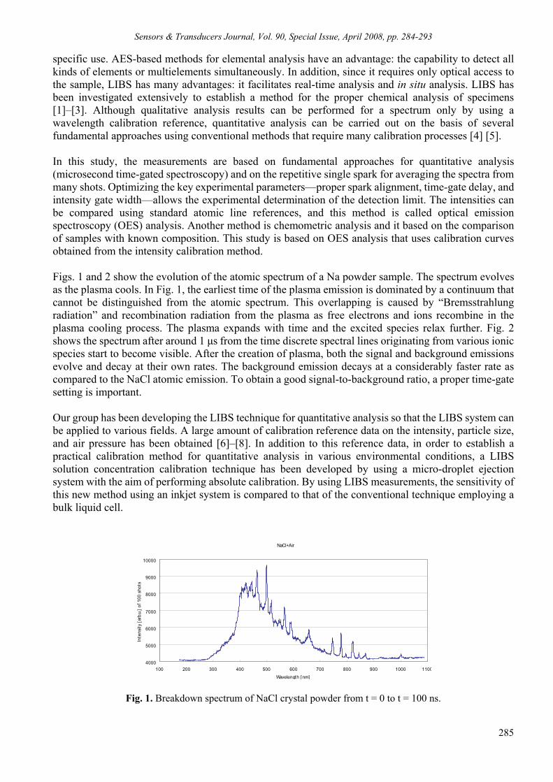
Sensors & Transducers Journal, Vol. 90, Special Issue, April 2008, pp. 284-293
285
specific use. AES-based methods for elemental analysis have an advantage: the capability to detect all kinds of elements or multielements simultaneously. In addition, since it requires only optical access to the sample, LIBS has many advantages: it facilitates real-time analysis and in situ analysis. LIBS has been investigated extensively to establish a method for the proper chemical analysis of specimens [1]–[3]. Although qualitative analysis results can be performed for a spectrum only by using a wavelength calibration reference, quantitative analysis can be carried out on the basis of several fundamental approaches using conventional methods that require many calibration processes [4] [5]. In this study, the measurements are based on fundamental approaches for quantitative analysis (microsecond time-gated spectroscopy) and on the repetitive single spark for averaging the spectra from many shots. Optimizing the key experimental parameters—proper spark alignment, time-gate delay, and intensity gate width—allows the experimental determination of the detection limit. The intensities can be compared using standard atomic line references, and this method is called optical emission spectroscopy (OES) analysis. Another method is chemometric analysis and it based on the comparison of samples with known composition. This study is based on OES analysis that uses calibration curves obtained from the intensity calibration method. Figs. 1 and 2 show the evolution of the atomic spectrum of a Na powder sample. The spectrum evolves as the plasma cools. In Fig. 1, the earliest time of the plasma emission is dominated by a continuum that cannot be distinguished from the atomic spectrum. This overlapping is caused by “Bremsstrahlung radiation” and recombination radiation from the plasma as free electrons and ions recombine in the plasma cooling process. The plasma expands with time and the excited species relax further. Fig. 2 shows the spectrum after around 1 µs from the time discrete spectral lines originating from various ionic species start to become visible. After the creation of plasma, both the signal and background emissions evolve and decay at their own rates. The background emission decays at a considerably faster rate as compared to the NaCl atomic emission. To obtain a good signal-to-background ratio, a proper time-gate setting is important. Our group has been developing the LIBS technique for quantitative analysis so that the LIBS system can be applied to various fields. A large amount of calibration reference data on the intensity, particle size, and air pressure has been obtained [6]–[8]. In addition to this reference data, in order to establish a practical calibration method for quantitative analysis in various environmental conditions, a LIBS solution concentration calibration technique has been developed by using a micro-droplet ejection system with the aim of performing absolute calibration. By using LIBS measurements, the sensitivity of this new method using an inkjet system is compared to that of the conventional technique employing a bulk liquid cell.
NaCl+Air
4000
5000
6000
7000
8000
9000
10000
100 200 300 400 500 600 700 800 900 1000 1100Wavelength [nm]
Inte
nsity
[arb
.u.]
of 1
00 s
hots
Fig. 1. Breakdown spectrum of NaCl crystal powder from t = 0 to t = 100 ns.

Sensors & Transducers Journal, Vol. 90, Special Issue, April 2008, pp. 284-293
286
NaCl+Air after 970[ns]
4000
4100
4200
4300
4400
4500
100 200 300 400 500 600 700 800 900 1000 1100Wavelength [nm]
Inte
nsity
[arb
.u.] b
y 10
0sho
ts
Fig. 2. Breakdown spectrum of NaCl crystal powder from t = 970 to t = 1070 ns. 2. Experimental Setup 2.1. Bulk Liquid Cell LIBS System This system is represented schematically in Fig. 3. The Nd:YAG laser (Big Sky Laser; model: Ultra) was controlled with the delay pulse generator (Stanford Research System, Inc., Model DG-535). The laser was operated at 1064 nm to generate a 50-mJ pulse with a width of 8 ns (FWHM). When used for ablation, the laser pulse was focused with a lens that had a focal length of 50 mm, thereby yielding a power density of 1012 W/cm2. Emissions from the laser-produced plasma were collected using additional lenses and they were then guided to a spectrograph (Chromex 250IS). Subsequently, the emitted light was dispersed using a diffraction grating with 1200 lines/mm and the electrical signal was recorded using a streak camera (Hamamatsu Photonics) with a time resolution of 10 ps or greater. Finally, the signal was processed and stored in a computer.
Fig. 3. Schematic representation of LIBS experiment using a bulk liquid cell. A comparison of the emissions focused (a) into the NaCl solution and (b) on the solution surface is shown in Fig. 4. The LIBS data obtained from the measurements were compared.
Streak cameraSpectrograph
Nd:YAG laser
Pulse generatorComputer
LensLenses
Breakdown cell
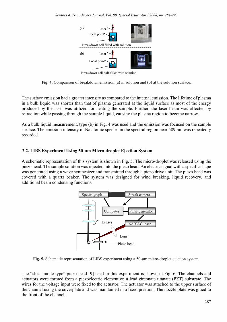
Sensors & Transducers Journal, Vol. 90, Special Issue, April 2008, pp. 284-293
287
Fig. 4. Comparison of breakdown emission (a) in solution and (b) at the solution surface. The surface emission had a greater intensity as compared to the internal emission. The lifetime of plasma in a bulk liquid was shorter than that of plasma generated at the liquid surface as most of the energy produced by the laser was utilized for heating the sample. Further, the laser beam was affected by refraction while passing through the sample liquid, causing the plasma region to become narrow. As a bulk liquid measurement, type (b) in Fig. 4 was used and the emission was focused on the sample surface. The emission intensity of Na atomic species in the spectral region near 589 nm was repeatedly recorded. 2.2. LIBS Experiment Using 50-µm Micro-droplet Ejection System A schematic representation of this system is shown in Fig. 5. The micro-droplet was released using the piezo head. The sample solution was injected into the piezo head. An electric signal with a specific shape was generated using a wave synthesizer and transmitted through a piezo drive unit. The piezo head was covered with a quartz beaker. The system was designed for wind breaking, liquid recovery, and additional beam condensing functions.
Fig. 5. Schematic representation of LIBS experiment using a 50-µm micro-droplet ejection system.
The “shear-mode-type” piezo head [9] used in this experiment is shown in Fig. 6. The channels and actuators were formed from a piezoelectric element on a lead zirconate titanate (PZT) substrate. The wires for the voltage input were fixed to the actuator. The actuator was attached to the upper surface of the channel using the coverplate and was maintained in a fixed position. The nozzle plate was glued to the front of the channel.
(a)
(b)
Laser
Laser
Focal point
Focal point
Breakdown cell filled with solution
Breakdown cell half-filled with solution
Nd:YAG laser
Pulse generatorComputer
Lens
Lenses
Spectrograph Streak camera
Piezo head

Sensors & Transducers Journal, Vol. 90, Special Issue, April 2008, pp. 284-293
288
Fig. 6. Structure of shear-mode-type piezo head.
Providing an electric field in a direction orthogonal to the polarization direction of the piezoelectric element leads to actuator winding transformation and the pressurization of the solution in the channel. Pressure was generated in the channel and it spread until the pressure wave was reflected between the nozzle and the solution supply area, and damped oscillations were generated when the pressure wave resonated. This mechanism caused the ejection of micro-droplets by receiving the pressure resonance over a period of time. 2.3. LIBS Experiment Using 30-µm Micro-droplet Ejection System A schematic representation of the LIBS system using a 30-µm NaCl solution droplet is shown in Fig. 7. The Nd:YAG laser was controlled with the delay pulse generator. The micro-droplet was released by using the dispenser head. Fig. 8 shows the scheme of the micro-droplet subsystem. The sample solution was injected into the piezo head. The micro-droplet generating electric signal was synchronized with the LED strobe output. The region with a continuous stream of micro-droplets was covered during wind breaking for protection from the fluctuation of the droplet position. Emissions from the laser-produced plasma were collected using additional lenses and were then guided to a spectrograph. The emissions were dispersed by the spectrograph and the resulting electrical signal was recorded using a streak camera. The signal was processed and stored in a computer.
Fig. 7. Schematic representation of LIBS experiment using a 30-µm droplet ejection system.
PZT electric field
cross-section (side view)
cross-section (top view)
shear stress
nozzle
polarization
channe
Computer
Lens
Lenses
Dispenser CCD
Nd:YAG laser
Pulse generator
Spectrograph Streak camera
Pulse generator
LEDMicro droplet sub system
coverplate

Sensors & Transducers Journal, Vol. 90, Special Issue, April 2008, pp. 284-293
289
Fig. 8. Schematic representation of micro-droplet sub system.
Fig. 9 shows the microphotograph of a micro-droplet ejection process. The micro-droplet nozzle ejected uniform droplets under stroboscopic illumination by an LED. The piezoelectric dispenser was capable of delivering up to 2000 droplets per second. The nozzle diameter was 30 µm. The droplet size could be varied in a narrow range by adjusting the voltage and voltage pulse duration. The velocity of the droplets increased with the voltage. Larger pulse duration led to larger droplets. In order to obtain the best stability and uniformity for the droplets, the optimum voltage parameters were set for every experiment. The piezoelectric nozzle was a droplet-on-demand device that provided single, isolated droplets with a diameter of 30 µm and an initial velocity of 2 m/s. For the purpose of synchronizing the laser pulses with individual droplets, laser plasma was generated in a gaseous environment.
Fig. 9. Photograph of micro-droplet ejection from a nozzle with a diameter of 30 µm. The photograph was taken under stroboscopic illumination at intervals of 50 µs from 150 µs to 300 µs after trigger.
3. Results and Discussion The breakdown emission intensities were obtained for 0.1 M to 1.0 M NaCl solutions by using a bulk liquid cell. Fig. 10 shows the error ranges of the Na D2 emission peak intensity. An analysis based on data obtained from 100 laser pulse shots indicated that the central gate point was 18.1 µs from trigger-in and the gate width was 3.9 µs. The analytical gate settings were optimized with 0.1 M NaCl solution. Generally, the intensity increased with the solution density up to 0.3 M. However, for higher concentrations this increase was not proportional, as expected. This indicated that the calibration curves were likely to have an optimum window for data collection. Some problems associated with the splashing of the sample solution were experienced when measurements were performed at the solution surface. With regard to the calibration, fluctuations in the droplet size distribution at the time of the laser spark caused problems.
LED CCD
Laser Spectrograph
Dispenser Windbreak Cell

Sensors & Transducers Journal, Vol. 90, Special Issue, April 2008, pp. 284-293
290
Error range at various NaCl concentrations
(0.1 M to 1.0 M) for 100 laser shots
0
100
200
300
400
500
600
0.1 0.2 0.3 0.4 0.5 0.6 0.7 0.8 0.9 1.0
NaCl solution [mol/ L]
Inte
nsity
[arb
.u.]
Fig. 10. Error range at various NaCl concentrations (0.1 M to 1.0 M) for 100 laser shots.
Figs. 11 and 12 show the LIBS experimental spectral data for the 0.1 M and 0.7 M NaCl solution samples. These data are presented as an example of data from comparison experiments for bulk-liquid and micro-droplet sampling techniques. The two different concentration samples were taken for the analysis using the 50-µm micro-droplet ejection system for comparison with the old bulk liquid method. The 0.1 M NaCl solution optimized the gate setting for obtaining the best signal-to-noise ratio. The 0.7 M NaCl solution showed the maximum error range for the old technique of bulk liquid measurement. An analysis based on data obtained from 100 laser pulse shots indicated that the gate setting was the same for micro-droplet ejection and the bulk liquid method. The micro-droplet ejection system was used for producing an improved calibration curve. LIBS with the micro-droplet ejection system produced intensities that were larger than conventional methods. A comparison of experimental data between the micro-droplet ejection system and the bulk liquid system is presented below. In Fig. 11, the data for the 0.1 M NaCl solution show that slightly difference between the two measurements. However, a significant difference occurred between the two measurements for the 0.7 M solution, as shown in Fig. 12. This clearly demonstrates that in the quantitative analysis of LIBS, a calibration curve determined using the micro-droplet technique cannot be used for the bulk liquid quantitation method.
Intensity improvement at 0.1M NaCl solution
4050
4550
5050
587 588 588 589 589 590 590 591 591
Wavelength [nm]
Inte
nsity
[arb
.u.]
Micro- droplet 0.1MOld bulk liquid 0.1M
Fig. 11. Intensity difference for 0.1 M NaCl solution between old technique of bulk liquid measurement and 50-µm micro-droplet measurement obtained from 100 laser pulse shots.

Sensors & Transducers Journal, Vol. 90, Special Issue, April 2008, pp. 284-293
291
Intensity improvement at 0.7M NaCl solution
4050
4550
5050
5550
6050
6550
587 588 588 589 589 590 590 591 591
Wavelength [nm]In
tens
ity [a
rb.u
.]
Micro- droplet 0.7MOld bulk liquid 0.7M
Fig. 12. Intensity difference for 0.7 M NaCl solution between old technique of bulk liquid measurement and 50-µm micro-droplet measurement obtained from 100 laser pulse shots.
Figs. 13 to 15 show the experimental data for 0.1 M to 0.3 M NaCl solution samples; these were obtained from a comparison between the LIBS spectral emission intensities obtained from the old bulk liquid method and those obtained from the 30-µm droplet ejection system. The gate settings were the same in the bulk liquid method and 50-µm droplet ejection system. In Fig. 13, the comparison of data for the 0.1 M NaCl solution between the 30-µm droplet ejection system and the bulk liquid method shows that the micro-droplet ejection system is more effective than the bulk liquid technique. Compared to Fig. 11, intensity difference for micro-droplet volume between 30-µm and 50-µm droplet was unclear. However, from a comparison between the micro-droplet technique and the bulk liquid technique, it was observed that both data showed the advantage of using the new LIBS solution measuring technique. Figs. 14 and 15 show a comparison between the data for the 0.2 M NaCl solution and those for the 0.3 M NaCl solution. From these data, the atomic spectral intensity is observed to increase with the density of the solution. Similar to the case of the 0.1 M NaCl solution, the micro-droplet intensity is higher than the bulk liquid technique. By using the comparison data for 0.1 M to 0.3 M NaCl Solution samples for this 30-µm micro-droplet ejection system, Na calibration curves are shown in Fig. 16. The calibration curves for Na were plotted by using the average intensity of five measurements, each with 100 laser shots. It appears that the plasma conditions were different among these setups. In the case of the plasma in the bulk liquid system, the plasma created by the laser dissipated its energy to its surroundings or constituents. In the laser-created plasma plume, the distribution of atoms was such that the inner core of the plume, which mostly contained excited species, was surrounded by the unexcited species of the outer layer.
Fig. 13. Intensity difference for 0.1 M NaCl solution between bulk liquid measurement performed using the old technique and 30-µm micro-droplet measurement obtained from 100 laser pulse shots.
Intensity improvement at 0.1M NaCl solution
40504150425043504450455046504750485049505050
587 588 588 589 589 590 590 591 591
Wavelength [nm]
Inte
nsity
[arb
.u.]
Micro- droplet0.1MOld bulk liquid0.1M
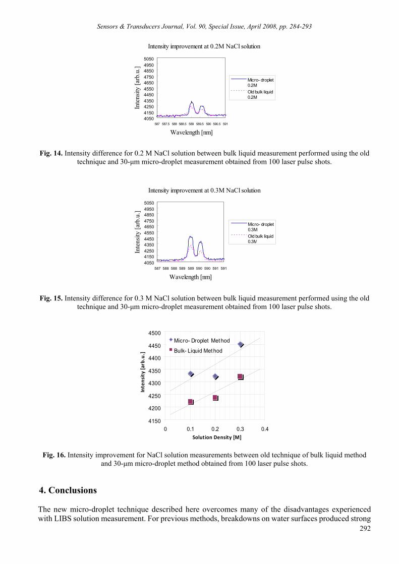
Sensors & Transducers Journal, Vol. 90, Special Issue, April 2008, pp. 284-293
292
Fig. 14. Intensity difference for 0.2 M NaCl solution between bulk liquid measurement performed using the old technique and 30-µm micro-droplet measurement obtained from 100 laser pulse shots.
Fig. 15. Intensity difference for 0.3 M NaCl solution between bulk liquid measurement performed using the old technique and 30-µm micro-droplet measurement obtained from 100 laser pulse shots.
4150
4200
4250
4300
4350
4400
4450
4500
0 0.1 0.2 0.3 0.4Solution Density [M]
Intensity [arb.u.]
Micro- Droplet Method
Bulk- Liquid Method
Fig. 16. Intensity improvement for NaCl solution measurements between old technique of bulk liquid method and 30-µm micro-droplet method obtained from 100 laser pulse shots.
4. Conclusions The new micro-droplet technique described here overcomes many of the disadvantages experienced with LIBS solution measurement. For previous methods, breakdowns on water surfaces produced strong
Intensity improvement at 0.3M NaCl solution
40504150425043504450455046504750485049505050
587 588 588 589 589 590 590 591 591
Wavelength [nm]
Inte
nsity
[arb
.u.]
Micro- droplet0.3MOld bulk liquid0.3M
Intensity improvement at 0.2M NaCl solution
40504150425043504450455046504750485049505050
587 587.5 588 588.5 589 589.5 590 590.5 591
Wavelength [nm]In
tens
ity [a
rb.u
.]
Micro- droplet0.2MOld bulk liquid0.2M

Sensors & Transducers Journal, Vol. 90, Special Issue, April 2008, pp. 284-293
293
emissions; however, the splashing of the sample at the water surface and chemical denaturation were practical and marked problems. For breakdowns passing through water, there was no splashing of the sample, but the emissions were very weak. In contrast, the new micro-droplet method described here, by micronizing the sample, made it possible for the entire volume of the liquid sample to be confined to the laser beam spot area and to be separated from the surrounding conditions. The advantages of this method were strong emissions, absence of splashing of the sample, solution density controllability, and absence of chemical denaturation. One disadvantage was that advanced timing control techniques were required. In the bulk liquid, most of the laser energy was used for vaporizing the sample. In contrast, the use of the micro-droplet ejection system allowed most of the laser energy to be consumed by ionizing the sample. Therefore, different data were obtained from each LIBS technique and different calibration curves were required even for the same solution. For the micro-droplet technique, the difference of emission could be caused by the balance between increased emission and absorption within the solution of delocalized and uniformly distributed NaCl particles. These results, to our knowledge, are important indications that micro-droplet output system which could generate same volume of sample has been employed in LIBS experiments. The technique needs to be developed further, but has the potential to overcome many of the problems associated with standard bulk-liquid-based techniques. References [1]. H. A. Archontaki and S. R. Crouch, Evaluation of an Isolated Droplet Sample Introduction System for
Laser-induced Breakdown Spectroscopy, Applied Spectroscopy, Vol. 42, No. 5, 1988, pp. 741–746. [2]. Christoph Janzen, Rüdiger Fleige, Reinhard Noll, Henrich Schwenke, Wilhelm Lahmann, Joachim Knoth,
Peter Beaven, Eckard Jantzen, Andreas Oest, Peter Koke, Analysis of Small Droplets with a New Detector for Liquid Chromatography Based on Laser-induced Breakdown Spectroscopy, Spectrochimica Acta Part B, Vol. 60, 2005, pp. 993–1001.
[3]. Akshaya Kumar, Fang Y. Yueh, Tracy Miller and Jagdish P. Singh, Detection of Trace Elements in Liquids by Laser-induced Breakdown Spectroscopy with a Meinhard Nebulizer, Applied Optics, Vol. 42, No. 30, 2003, pp. 6040–6046.
[4]. Liang Xu, Valery Bulatov, Vladimir V. Gridin and Israel Schechter, Absolute Analysis of Particulate Materials by Laser-induced Breakdown Spectroscopy, Analytical Chemistry, Vol. 69, No. 11, 1997, pp. 2103–2108.
[5]. Susumu Nakamura, Yoshiro Ito, Kazuhiro Sone, Hitoshi Hiraga and Kenichi Kaneko, Determination of an Iron Suspension in Water by Laser-induced Breakdown Spectroscopy with Two Sequential Laser Pulses, Analytical Chemistry, Vol. 68, No. 17, 1996, pp. 2981–2986.
[6]. Muneaki Wakamatsu and Toshitsugu Ueda, Particle Measurement Using LIBS, SICE Annual Conference 2005 in Okayama, 2005, pp. 3717–3720.
[7]. Alexander Andreev and Toshitsugu Ueda, Simulation of Laser Plasma Emission Characteristics of Small Solid Particles in Different Gas Atmospheres at Various Pressures, Trans. IEE of Japan, Vol. 121-E, No. 11, 2001, pp. 593–598.
[8]. Muneaki Wakamatsu, Satoshi Ikezawa and Toshitsugu Ueda, Particle Element and Size Simultaneous Measurement Using LIBS, Trans. IEE of Japan, Vol. 127-E, No. 9, 2007, pp. 397-402.
[9]. Yoshio Takeuchi and Shinichi Nishi, Features of Shear Mode Piezo Inkjet Head, Journal of the Imaging Society of Japan, Vol. 43, No. 6, 2004, pp. 509–514.
___________________
2008 Copyright ©, International Frequency Sensor Association (IFSA). All rights reserved. (http://www.sensorsportal.com)

Sensors & Transducers Journal, Vol. 90, Special Issue, April 2008, pp. 294-301
294
SSSeeennnsssooorrrsss &&& TTTrrraaannnsssddduuuccceeerrrsss
ISSN 1726-5479© 2008 by IFSA
http://www.sensorsportal.com
A Forward Solution for RF Impedance Tomography in Wood
1Ian WOODHEAD, 2Nobuo SOBUE, 1Ian PLATT, 3John CHRISTIE 1Lincoln Technology
Lincoln Ventures Ltd, Lincoln University, New Zealand 2Faculty of Agriculture
Shizuoka University, Shizuoka, 422-8529, Japan 3Streat Technology Ltd.
c/o Lincoln Ventures Ltd, Lincoln University, New Zealand, E-mail: [email protected], [email protected], [email protected], [email protected]
Received: 15 October 2007 /Accepted: 20 February 2008 /Published: 15 April 2008 Abstract: Both integral equation and differential equation methods enable modelling current and hence impedance of wood, to provide the forward solution for impedance tomography that in turn provides a measure of its internal moisture distribution. Previously, we have used a series impedance model and successfully demonstrated measurement of internal moisture distribution. Here we describe the adaptation of our integral equation method for this application. This has required an alternative calculation to model the impressed field from the segmented electrodes used in the measurements to date, and we demonstrate distortion of the anomalous field due to the presence of a wood dielectric, and the field magnitude. Further work will be required to translate the resulting field distribution from our model, to complex current and hence impedance readings, to allow completion of tomographic reconstruction using this approach. Copyright © 2008 IFSA. Keywords: Impedance, Tomography, Heterogeneous, Model, Wood 1. Introduction Water has several distinctive properties that may be used for measurement of moisture content in composite materials. One is that the bond angle of 104.47 degrees [1] between the hydrogen atoms, combines with the differing electronegativity of the hydrogen (2.1) and oxygen (3.5) atoms to result in a large polar moment. The strong polar nature of the water molecule contributes to the large relative permittivity ( )rε of approximately 80 for bulk water compared to that of most dry biological and

Sensors & Transducers Journal, Vol. 90, Special Issue, April 2008, pp. 294-301
295
natural materials for which rε is generally in the range 2 to 5 [2]. This large contrast enables dielectric measurements of composite materials to form a useful indirect measurement of volumetric moisture content ( )vθ . In practice, rε is a curvilinear function of vθ , whose curvature is dependent on the composite material, its texture, and its porosity which influence the interaction of the composite material with water.
rε arises primarily from polar molecules that store energy by elastic rotation, but contributions are also made by elastically altering bond angles, and intra-atomic contributions that are dominated by distortion of electron distribution. In the absence of an electric field, a polar substance such as water has permanent dipole moments that are randomly distributed so that no net polarization is present. The conductivity of the material and any conducting inclusions (e.g. dissociated water) dispersed within the material contribute to the dielectric loss of the mixture. The total permittivity ε comprises a real component 'ε that represents the real or energy storage component of the permittivity, and "ε the orthogonal or imaginary component that results from the conduction current contributed to by conductivity and other forms of dielectric loss. ' "jε ε ε= − , (1) where j is 1− . Many methods of determining 'ε are usefully employed for determining vθ of composite materials. However where "ε is large in comparison with 'ε , the measurement becomes inaccurate [3]. Consequently, the choice of measurement frequency range when measuring 'ε is crucial since many loss processes are frequency dependent. For measurement of moisture content in wood, both 'ε and "ε have been explored such as described by [4], and provided the frequency is chosen to avoid the dispersive low frequency regions either or both measures may be used to provide a useful indication of moisture content. We [5] have demonstrated the utility of applying impedance tomography to measurement of the internal moisture distribution in wood (Fig. 1), and using time domain reflectometry techniques [6]. Here we apply the electromagnetic model of [7] to the impedance tomography problem described by [5].
Fig. 1. Configuration of the segmented electrodes for measurement of the internal moisture distribution in wood
described by Sobue and Inagaki (2007). There are two main advantages of an integral equation model for this type of problem. The first is that since only the anomalous region (that occupied by the wood) needs to be modelled, the domain of the
Guard electrode
Segmented electrodes
1 2 3 4 5 6
Common electrode

Sensors & Transducers Journal, Vol. 90, Special Issue, April 2008, pp. 294-301
296
problem need only include the timber cross-section and the segmented electrodes or capacitor plates (Fig. 1); the region beyond makes no contribution. Using a differential equation model, requires setting external boundary conditions, which may include the electrodes, but for accurate modelling needs to extend well beyond the region of the wood to where the field may be assumed to be zero. The second advantage of an integral equation approach is that the problem may be solved once for a given moisture distribution and for any field distribution representing different segments of the electrodes, resulting in just one forward calculation per inverse iteration. Again this contrasts with differential equation methods where one solution would be required for each capacitor electrode configuration. The approach is thus generally more favourable for inverting measurements than the otherwise more rapid differential equation methods. We first provide some background to the integral equation approach, and then explain how we configured the impressed or incident field for application to this problem and show results from that simulation. Finally we describe the remaining work to complete the solution. 2. Theory The polarization of a discretized zone or cell within a dielectric material may be represented by a dipole at its geometric centre. In most dielectric materials, there is no net polarization until generated by an external or impressed field. When applied to this quasi-static electric field problem where the material is considered lossless, the method of moments may be considered as the summation in each cell of the electric field contributions due to the polarization in all other cells. Using rectangular coordinates, the potential φ p at point p(x, y, z) generated by polarization P, is:
φπεpP r
r=
∧~.4 0
2 , (2)
where r∧
is a unit vector pointing from the centre of the cell to p [8], and r is the distance from the cell centre to p. In Cartesian 3-space:
30
.( , , )4p
P x y zr
φπε
=% % % %
, (3)
where ~, ~ ~x y z and are the rectangular components of ~r . The potential arising from the contribution from many cells is:
φπεP =
∧
∫∫∫~.P r
rdv
4 02 , (4)
where dv is the differential volume over which each P. r∧
applies. Reverting to the single dipole case, its electric field is the space rate of change of potential ( pφ−∇ ) so that from equation 3:
Epx =−
⋅ − − −⎡⎣⎢
⎤⎦⎥
∧ ∧ ∧~( ) ( ) ( )P
rx r x y xy z xz
43 3 3
05
2 2
πε (5)
with corresponding equations for Epy and Epz. The above may be combined in an integral equation describing the electric field Ep at a point p:

Sensors & Transducers Journal, Vol. 90, Special Issue, April 2008, pp. 294-301
297
E P.r
P ( , , ) ( )x y zr
dv= −∇∧
∫∫∫ 4 02πε
(6)
The polarization region may now be discretized, and following the method of moments [9], we calculate the matrix of polarization vectors P(x, y, z) using: L x y z
x y z x y zx y z
( ) ( , , )
( , , ) ( , , )( , , )
P E
E Pi
P
= −
= −ε χ0
, (7)
where L is a linear operator, Ei the external impressed field and χ(x, y, z) the electric susceptibility (εr (x, y, z) - 1). Equation 7 is converted to matrix form and solved for the vector of polarizations P, and the electric field strength in each cell is recovered from the polarization:
E P( , , ) ( , , )( , , )
x y z x y zx y z
=ε χ0
(8)
The model used here employs the pseudo 3-D method [7] which effectively reduces the problem to 2-D, and uses field proximity compensation as described in [6] to obtain improved prediction of the electric field distribution. The inputs required to solve the forward solution are: 1. A vector describing the impressed field 2. A matrix describing the complex permittivity within each cell 3. Details of the dimensionality of the problem. While the above method applies to any impressed field distribution, in this case Ei is the vector of impressed field components arising from two planar electrodes as in Fig. 1. 3. Modelling Planar Electrodes To calculate the field from two planar electrodes, and continuing to use rectangular coordinates, we first define a small element of the planar electrode x∆ , with a line charge density ρ and calculate the potential at a point p positioned a distance 2 2r x y= + from the electrode element [8]. From electrostatic theory, e.g. [8], the x-component of the potential is defined as:
2 204
xx
x yρφ
πε∆
=+
(9)
Since the electric field E is the gradient of the potential, i.e. φ= −∇E , and using (9) to define the potential in the x and y directions, it can be shown that the two rectangular components of the field at p may be expressed as:
( ) ( )
( )
1 32 2 2 22 2
0
32 2 2
0
4
4
x
y
x y x x y dx
y x y dy
ρπε
ρπε
− −
−
⎛ ⎞= + − +⎜ ⎟
⎝ ⎠
= − +
∫
∫
E
E
(10)

Sensors & Transducers Journal, Vol. 90, Special Issue, April 2008, pp. 294-301
298
The integrals are taken over the surfaces of both electrodes with appropriate consideration to the sign of ρ. Then applying the theory described in Section 2, the resultant electric field may be generated. Fig. 2 shows the incident or impressed electric field, when no wood is inserted between the electrodes, when using equations 10 to provide a vector of impressed field values in the model.
0 2 4 6 8 10 12 14 16 180
2
4
6
8
10
12
14
16
18
Fig. 2. Cross-sectional view (as in Fig. 1) showing the incident electric field distribution from two planar electrodes in air.
A typical result is shown in Fig. 3. In this case it arises from the forward solution applied to the region where a block of wood, 3 3r jε = + , is positioned in the upper left region between the planar electrodes. It demonstrates the reduced field intensity within the wood compared with air, and the distortion of the surrounding field compared with Fig. 2. Note that in this instance, the electrodes have been defined as zero thickness, so there is an anomalous impact on the field outside the electrodes. The simplification has no effect on the field between the electrodes, with or without an included dielectric.
0 2 4 6 8 10 12 14 16 180
2
4
6
8
10
12
14
16
18
Fig. 3. Cross-sectional view (as in Fig. 2) showing the predicted electric field distribution when a block of wood is placed in the upper left region between the two planar electrodes.
4. Validation We chose to validate the model by modelling the displacement current and hence predicting the capacitance of two planar electrodes with a PVC dielectric. A PVC block with 3 0r jε = + and with dimensions 50 by 50 by 148 mm was fitted with two self-adhesive foil electrodes of dimension 50 by

Sensors & Transducers Journal, Vol. 90, Special Issue, April 2008, pp. 294-301
299
148 mm to form a capacitor. The measured capacitance, due to that of the capacitor itself plus the free-space capacitance of one plate at 250 kHz was 18.39 pF, so that the expected current from a 1V RMS source was 14.75 µA. The above model with a permittivity between the electrodes of 3 0r jε = + , was used to calculate the electric field distribution for a potential difference between the electrodes of 1V RMS at 250 kHz. The displacement current density JD, defined as dD dt where D is electric displacement [11], can be written:
0(1 )DdEJdt
χ ε= + (11)
and hence the current is defined as: 2
0(1 )DdEi ldt
χ ε= + (12)
where l is the edge length of the cubic cells. dE dt for each cell was taken as the RMS value of the maximum dE dt at 250 kHz, Eω . Since the forward solution represents the electrodes as sheet charge sources rather than conductors, the field and hence current outside the electrodes is affected by the dielectric between the electrodes. Hence the simulated displacement current has been taken as the sum of the total current with 1 0r jε = + and the difference between the current integrated along the inner face of the electrodes for the conditions 3 0r jε = + and 1 0r jε = + . This provided a value of 15.14 µA, compared with the 14.75 µA value derived from measurements.
0 2 4 6 8 10 12 14 16 180
2
4
6
8
10
12
14
16
18
Fig. 4. Predicted displacement current for PVC dielectric between two planar electrodes. 5. Measurements in Wood The validated forward solution described above is the major remaining step in providing a new impedance tomography method for measurement of moisture distribution in wood. The method of [5], configured according to Fig. 1, employed an instrument to measure the real and imaginary components of the impedance at 250 kHz. For an iterative inversion procedure to predict moisture distribution, the forward solution will need to be configured to predict the impedance between combinations of electrode segments which would then be compared with the measured values.

Sensors & Transducers Journal, Vol. 90, Special Issue, April 2008, pp. 294-301
300
We explained above how an integral equation method conveys advantages for inverse methods, since little computational effort is required to provide a solution for each different configuration of the impressed field. In the method described by [5], guard electrodes were used, and hence we may make the approximation that the gaps between the electrode segments are arbitrarily narrow. In this case then, the electric field and current distribution remain constant, irrespective of which electrode segment is being measured, so that one forward calculation will suffice for each estimate of the wood impedance distribution in the inverse solution. A further feature of this approach is that there is little computational overhead in providing values of impedance for many different measurement frequencies, and use of multiple frequencies is commonly used to extract a measure of product density. Hence we are keen to extend this work in the future to measurement of density distribution. 6. Conclusions We have described a forward solution for calculating the impedance distribution in wood from its dielectric properties, and shown simulations of the electric field distribution in wood from the field of two parallel electrodes. The computational efficiency of the integral equation model has also been described and we forecast that this will have important industrial benefits. We have also predicted the displacement current in a PVC dielectric and provided good agreement with the measured value at 250 kHz. The next stage, is to apply the method to our earlier work which used a series model of impedance to provide tomographic reconstruction of the moisture distribution in wood. Acknowledgement This work was supported by the New Zealand Foundation for Research Science and Technology. References [1]. F. Franks, Water, a comprehensive treatise, Vol. 1. The physics and physical chemistry of water, Ed. by
J. B. Hastead, Plenum Press, London, 1972. [2]. S. O. Nelson, Electrical properties of agricultural products, a critical review, ASAE special publication
SP-05-73, St Joseph, MI-ASAE, 1973. [3]. W. Leschnik and U. Schlemm, Measurement of the moisture and salt content of building materials, 3rd
Workshop on Electromagnetic Wave Interaction with Water and Moist Substances, USDA, Athens, Georgia, 1999.
[4]. G. I. Torgovnikov, Dielectric properties of wood and wood-based materials, Ed. by T. E. Timel, Springer Verlag, Berlin, 1993.
[5]. N. Sobue and M. Inagaki, 7th Conference on Electromagnetic Wave Interaction with Water and Moist Substances, Hamamatsu, Japan, 2007.
[6]. I. M. Woodhead, P. Riding, J. H. Christie and G. D. Buchan, Non-Invasive Measurement of Moisture Distribution, Proceedings of the 2004 New Zealand National Conference on Non Destructive Testing, Massey University, NZ, 2004.
[7]. I. M. Woodhead, G. D. Buchan and D. Kulasiri. Pseudo-3-D Moment method for rapid calculation of electric field distribution in a low-loss inhomogeneous dielectric, IEEE Transactions on Antennas and Propagation, 49, 8, 2001, pp. 1117-1122.
[8]. A. F. Kip, Fundamentals of Electricity and Magnetism, McGraw-Hill, 1962. [9]. R. F. Harrington, Field Computation by Moment Methods, R E Kreiger, 1968.

Sensors & Transducers Journal, Vol. 90, Special Issue, April 2008, pp. 294-301
301
[10]. I. M. Woodhead, G. D. Buchan, I. G. Platt and J. H. Christie, Enhanced Integral Equation Modelling for Moisture Sensors, Sixth Conference on Electromagnetic Wave Interaction with Water and Moist Substances, Weimar, Germany, 2005, pp. 132-139.
[11]. S. Ramo, J. R. Whinnery, and T. Van Duzer, Fields and Waves in Communication Electronics, Wiley, 1993.
[12]. I. M. Woodhead, G. D. Buchan, I. G. Platt and J. H. Christie, 7th Conference on Electromagnetic Wave Interaction with Water and Moist Substances, Hamamatsu, Japan, 2007.
___________________
2008 Copyright ©, International Frequency Sensor Association (IFSA). All rights reserved. (http://www.sensorsportal.com)

Sensors & Transducers Journal, Vol. 90, Special Issue, April 2008, pp. 302-309
302
SSSeeennnsssooorrrsss &&& TTTrrraaannnsssddduuuccceeerrrsss
ISSN 1726-5479© 2008 by IFSA
http://www.sensorsportal.com
A Micromachined Infrared Senor for an Infrared Focal Plane Array
Seong M. Cho, Woo Seok Yang, Ho Jun Ryu, Sang Hoon Cheon, Byoung-Gon Yu,
Chang Auck Choi IT Convergence & Components Laboratory (ICCL), Electronics and Telecommunications Research
Institute (ETRI), 161 Gajeong-dong, Yuseong-gu, Daejeon, Korea Tel.: +82-42-860-6237, fax: +82-42-860-6205
E-mail: [email protected], www.etri.re.kr
Received: 15 October 2007 /Accepted: 20 February 2008 /Published: 15 April 2008 Abstract: A micromachined infrared sensor for an infrared focal plane array has been designed and fabricated. Amorphous silicon was used as a sensing material, and silicon nitride was used as a membrane material. To get a good absorption in infrared range, the sensor structure was designed as a λ/4 cavity structure. A Ni-Cr film was selected as an electrode material and mixed etching scheme was applied in the patterning process of the Ni-Cr electrode. All the processes were made in 0.5 µm iMEMS fabricated in the Electronics and Telecommunication Research Institute (ETRI). The processed MEMS sensor had a small membrane deflection less than 0.15 µm. This small deflection can be attributed to the rigorous balancing of the stresses of individual layers. The efficiency of infrared absorption was more than 75% in the wavelength range of 8 ~ 14 µm. The processed infrared sensor showed high responsivity of ~230 kV/W at 1.0V bias and 2 Hz operation condition. The time constant of the sensor was 8.6 ms, which means that the sensor is suitable to be operated in 30 Hz frame rate. Copyright © 2008 IFSA. Keywords: Infrared Sensor, MEMS, Focal Plane Array 1. Introduction The demands for infrared image sensors have been increased during last a few decades. Their application fields have been widened to civil applications beyond military interests. Recently developed civil application fields require uncooled type image sensors, which are much cheaper than cooled type sensors.

Sensors & Transducers Journal, Vol. 90, Special Issue, April 2008, pp. 302-309
303
Pyroelectric type and bolometer type are two representative types in the uncooled infrared image sensors. For the case of the pyroelectric type sensors, the theoretical performances are the best among the uncooled type sensors but they need chopping operation of incident light. The use of chopper makes it difficult to minimize system size and power consumption. For these reasons, recent researches on the uncooled infrared image sensors are mainly focused on the bolometer type sensors. Vanadium oxide has been the base sensing material in the bolometer type sensors for the past two decades [1]. It has relatively high thermal coefficient of resistance (TCR) and good noise properties. But, recently amorphous silicon (a-Si) has been tried as a sensing material, and it makes a competition with vanadium oxide based materials [2-4]. The amorphous silicon is weaker than vanadium oxide in the respect of noise performances, but its process is much easier and has merits in the respect of uniformity and reproducibility. In the present study, a MEMS sensor structure for a bolometer type image sensor was designed and fabricated. Amorphous silicon was selected as a sensing material. A Ni-Cr film which has low thermal conductivity was selected as an electrode material to maximize the sensor responsivity and mixed etching scheme was applied in the patterning process of the Ni-Cr electrode. The stress values of each consititutional layers were analyzed and rigorously balanced to minimize the membrane deflection. Considering monolithic integration with read-out integrated circuit (ROIC), the structure and the processes were designed to be fully compatible with CMOS process. The processed sensor showed good optical response properties. The responsivity of the sensor was ~50 kV/W at 0.5V bias and 30 Hz operation condition. The measured thermal time constant was ~8.6 ms. 2. Design of Sensor Structure 2.1. Vertical Structure Fig. 1 is a schematic diagram showing the vertical structure of the unit pixel. Amorphous silicon was adapted as a sensor material. Silicon nitride was used as membrane layers. To get a good absorption in infrared range, the sensor was designed as a λ/4 cavity structure [5]. With λ/4 cavity structure, the absorption of light is interferometrically enhanced. Considering the wavelength range of operation, the height of the gap between the sensor membrane and the underlying reflector was designed as 2 µm, which was controlled by the thickness of the sacrificial layer. The reflector was made with sputtered Al film. A thin TiN film was used as an absorption layer. The thickness of TiN layer was controlled to have 377 Ω of sheet resistance, which corresponds to the optimum value to get perfect absorption in λ/4 cavity structure [5].
ThermalInsulation cut
Si wafer
SiO2 IMD(Inter- Metal Dielectric)300 nm Al reflectorBias- pad
λ /4 gap (~ 2µm) using sacrificial polyimide Anchor
a- Si
Fig. 1. Vertical structure of the designed sensor.

Sensors & Transducers Journal, Vol. 90, Special Issue, April 2008, pp. 302-309
304
Considering the monolithic process with read-out integrated circuit (ROIC) by post CMOS micromachining processes, polyimide (PI2545, HD Microsystems Co., USA) was selected as a sacrificial layer, which can be processed in a low temperature, typically less than 400 oC. The pitch of the unit pixel was 50 µm, and filling factor was more than 77 %. 2.2. Thermal Design Thermal parameters are very important in designing of IR sensors, which influence responsivity and speed of sensor. Two important thermal parameters are thermal conductance (G) and thermal time constant (τ). Thermal conductance influences responsivity of sensor with following relation [6].
2/1222 )41( τπαεfG
BIRR+
= , (1)
where B is the bridging factor, I is the bias current, R is the detector resistance, α is the temperature coefficient of resistance, ε is the absorptivity, G is the thermal conductance, f is the operating frequency, and τ is the detector time constant, which is defined as follow: GC /=τ , (2) where C is the thermal capacity of the sensor membrane. The thermal time constant determines the speed of sensor response. Too small value of the time constant deteriorates signal amplitude and too large value make it impossible to be operated in a suitable frame rate. Therefore, there exists an optimum value in the thermal time constant. To be operated with 30 Hz frame rate, ~ 10 ms is the optimum value. The thermal parameters were controlled by varying the width of the legs in structure design. The width of legs was variably designed from 1 µm to 2 µm. For the case of the sensor structure with the legs of 2 µm width, the designed thermal conductance was ~ 1.5 x 10⁻⁷ J/K. And corresponding thermal time constant was ~10 ms. 3. Process 3.1. Process Overview Fig. 2 is a schematic diagram showing the process of the infrared sensor. An aluminium film with thickness of 3000Å, which acts as a reflector, was deposited and patterned by lithography process on an insulation oxide layer. Then, polyimide, which acts as a sacrificial layer, was spin-coated and cured. The coated polyimide layer was patterned to make anchor areas by lithographic process and dry etching. Then, the first nitride layer was deposited by plasma enhanced chemical vapor deposition process (PECVD) with thickness of 500Å. After deposition of the first nitride layer, TiN layer, which acts as an absorption layer, was deposited by sputtering process. The thickness of TiN layer was 100Å, which corresponds to the sheet resistance value of 377 Ω. The TiN absorption layer was patterned by lithography and dry etching process. Followed by patterning of the TiN layer, the second nitride layer was deposited by PECVD process. Then, contact holes for electrical connection were formed in the anchor areas. After formation of the contact holes, electrode metal was deposited and patterned. A Ni-Cr film with thickness of 500Å was used as an electrode material. Followed by patterning of the electrodes, a-Si film was deposited by PECVD process with thickness of 1500Å. Then, protection silicon nitride was deposited by PECVD process. After deposition of protection nitride, membrane was

Sensors & Transducers Journal, Vol. 90, Special Issue, April 2008, pp. 302-309
305
patterned and dry etched. Finally, Removal of the polyimide sacrificial layer was done with oxygen plasma. Fig. 3 shows the SEM images of the processed sensor. As can be seen from the figure, the MEMS structure for an infrared sensor could be successfully fabricated. All the processes used in the fabrication were fully CMOS compatible. Therefore, these processes can be directly applied to the fabrication of monolithic type sensors.
Step 1.- Reflector (Al) deposition & patterning
Step 2.- Polyimide coating & patterning
Step 3.- Nitride deposition - Absorption layer deposition & patterning- Nitride deposition
Step 4. - Electrode deposition & patterning- a- Si deposition
Step 5. - Nitride deposition
Step 6.- Membrane patterning & release
Fig. 2. Schematic diagram showing the processes of the sensor structure.
(a)
(b) Fig. 3. SEM micrographs of the processed pixel array ; (a) 45o tilt view, (b) 80o tilt view. The pixel pitch is 50 µm,
and the width of the isolation leg is 2 µm.
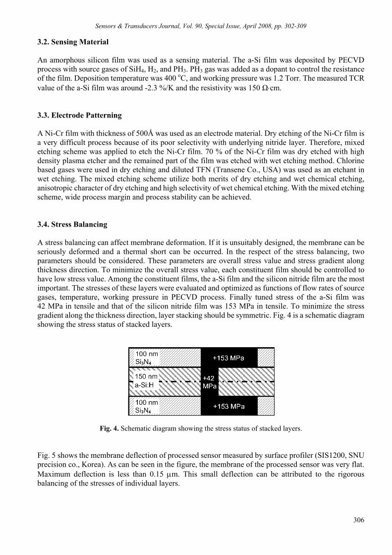
Sensors & Transducers Journal, Vol. 90, Special Issue, April 2008, pp. 302-309
306
3.2. Sensing Material An amorphous silicon film was used as a sensing material. The a-Si film was deposited by PECVD process with source gases of SiH4, H2, and PH3. PH3 gas was added as a dopant to control the resistance of the film. Deposition temperature was 400 oC, and working pressure was 1.2 Torr. The measured TCR value of the a-Si film was around -2.3 %/K and the resistivity was 150 Ω⋅cm. 3.3. Electrode Patterning A Ni-Cr film with thickness of 500Å was used as an electrode material. Dry etching of the Ni-Cr film is a very difficult process because of its poor selectivity with underlying nitride layer. Therefore, mixed etching scheme was applied to etch the Ni-Cr film. 70 % of the Ni-Cr film was dry etched with high density plasma etcher and the remained part of the film was etched with wet etching method. Chlorine based gases were used in dry etching and diluted TFN (Transene Co., USA) was used as an etchant in wet etching. The mixed etching scheme utilize both merits of dry etching and wet chemical etching, anisotropic character of dry etching and high selectivity of wet chemical etching. With the mixed etching scheme, wide process margin and process stability can be achieved. 3.4. Stress Balancing A stress balancing can affect membrane deformation. If it is unsuitably designed, the membrane can be seriously deformed and a thermal short can be occurred. In the respect of the stress balancing, two parameters should be considered. These parameters are overall stress value and stress gradient along thickness direction. To minimize the overall stress value, each constituent film should be controlled to have low stress value. Among the constituent films, the a-Si film and the silicon nitride film are the most important. The stresses of these layers were evaluated and optimized as functions of flow rates of source gases, temperature, working pressure in PECVD process. Finally tuned stress of the a-Si film was 42 MPa in tensile and that of the silicon nitride film was 153 MPa in tensile. To minimize the stress gradient along the thickness direction, layer stacking should be symmetric. Fig. 4 is a schematic diagram showing the stress status of stacked layers.
Fig. 4. Schematic diagram showing the stress status of stacked layers. Fig. 5 shows the membrane deflection of processed sensor measured by surface profiler (SIS1200, SNU precision co., Korea). As can be seen in the figure, the membrane of the processed sensor was very flat. Maximum deflection is less than 0.15 µm. This small deflection can be attributed to the rigorous balancing of the stresses of individual layers.

Sensors & Transducers Journal, Vol. 90, Special Issue, April 2008, pp. 302-309
307
Fig. 5. Membrane deflection of the processed sensor measured by surface profiler. 4. Characterization 4.1. Absorbance in Infrared Range Fig. 6 shows the infrared absorption properties of the processed sensor. The absorption property was measured with IR spectrometer (ISS66, Bruker Co., USA) with incident angle of 85o. The infrared absorption efficiency of the processed sensor was more than 75 % in the wavelength range 8-14 µm. The absorption efficiency of 8-9 µm range is relatively lower than that of 10-14 µm range. This is because there are phonon bands of nitride around the wavelength of 10 µm. The nitride films, which were used as membrane layers, have anomalously high refractive index and high attenuation coefficient in that wavelength range [7].
Fig. 6. Infrared absorption property of the processed sensor. 4.2. Infrared Responses Fig. 7 shows the measurement system used for infrared response. The processed sensor was vacuum packaged and a simple linear amplifier with unit gain was used as a transducer circuit. A blackbody was used as an infrared source. Fig. 8 shows the measured infrared response of the processed sensor. The blue lines are chopper signals and the red lines are output signals of the sensor. The responsivity of the
0 10 20 30 40 50
1.0
1.5
2.0
2.5
0.15 µm
Hei
ght (µm
)
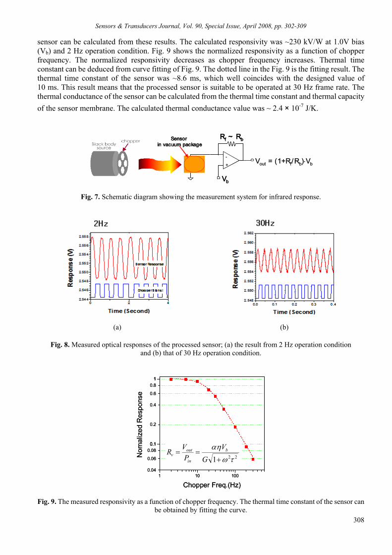
Sensors & Transducers Journal, Vol. 90, Special Issue, April 2008, pp. 302-309
308
sensor can be calculated from these results. The calculated responsivity was ~230 kV/W at 1.0V bias (Vb) and 2 Hz operation condition. Fig. 9 shows the normalized responsivity as a function of chopper frequency. The normalized responsivity decreases as chopper frequency increases. Thermal time constant can be deduced from curve fitting of Fig. 9. The dotted line in the Fig. 9 is the fitting result. The thermal time constant of the sensor was ~8.6 ms, which well coincides with the designed value of 10 ms. This result means that the processed sensor is suitable to be operated at 30 Hz frame rate. The thermal conductance of the sensor can be calculated from the thermal time constant and thermal capacity of the sensor membrane. The calculated thermal conductance value was ~ 2.4 × 10⁻⁷ J/K.
Vout = (1+Rf/Rb)⋅Vb-
+
-
Rb
Rf ~ Rb
Vb
Sensor in vacuum package
Vout = (1+Rf/Rb)⋅Vb-
+
-
Rb
Rf ~ Rb
Vb
Sensor in vacuum package
-
+
-
Rb
Rf ~ Rb
Vb
Sensor in vacuum package
Fig. 7. Schematic diagram showing the measurement system for infrared response.
(a)
(b)
Fig. 8. Measured optical responses of the processed sensor; (a) the result from 2 Hz operation condition and (b) that of 30 Hz operation condition.
1 10 1000.04
0.06
0.080.10.1
0.2
0.4
0.6
0.811
Nom
aliz
ed R
espo
nse
Chopper Freq.(Hz)
221 τωαη+
==G
VP
VR b
in
outv
1 10 1000.04
0.06
0.080.10.1
0.2
0.4
0.6
0.811
Nom
aliz
ed R
espo
nse
Chopper Freq.(Hz)
221 τωαη+
==G
VP
VR b
in
outv
Fig. 9. The measured responsivity as a function of chopper frequency. The thermal time constant of the sensor can
be obtained by fitting the curve.

Sensors & Transducers Journal, Vol. 90, Special Issue, April 2008, pp. 302-309
309
5. Conclusions A micromachined sensor part for an uncooled type infrared image sensor based on a-Si sensing material has been designed and fabricated. The MEMS sensor part was successfully fabricated with polyimide sacrificial layer. A Ni-Cr film with low thermal conductivity was adapted as an electrode material and mixed etching scheme was applied in the patterning process of the Ni-Cr electrode. All the processes used in the fabrication were fully CMOS compatible. Therefore, these processes can be directly applied to the fabrication of monolithic type sensors. The processed MEMS sensor had a small membrane deflection less than 0.15 µm. This small deflection can be attributed to the rigorous balancing of the stresses of individual layers. The efficiency of infrared absorption was more than 75 % in the wavelength range 8 ~ 14 µm. The responsivity of the sensor was ~230 kV/W at 1.0 V bias and 2 Hz operation condition. The time constant of the sensor was ~8.6 ms, which means that the sensor is suitable to be operated in 30 Hz frame rate. Acknowledgements This work was supported by the IT R&D program of MIC/IITA [2006-S054-01, Development of CMOS based MEMS processed multi-functional sensor for ubiquitous environment]. References [1]. S. M. Cho et al, Design and fabrication of a MEMS sensor for an Infrared Focal Plane Array, in Proceedings
of 2nd International Conference on Sensing Technology, 2007. [2]. D. Murphy et. al., Expanded applications for high performance VOx microbolometer FPAs, in Proceedings
of SPIE, Vol. 5783, 2005, pp. 448-459. [2]. J. J. Yon et al, First demonstration of 25um pitch uncooled amorphous silicon microbolometer IRFPA at
LETI-LIR, in Proceedings of SPIE, Vol. 5783, 2005, pp. 432-440. [3]. M. Almasri, B. Xu, and J. Castracane, Amorphous Silicon Two-Color Microbolometer for Uncooled IR
Detection, IEEE Sensors Journal, Vol. 6, No. 2, 2006, pp. 293-300. [4]. J. L. Tissot et al, High performance and low thermal time constant amorphous silicon based 320 × 240
uncooled microbolometer IRFPA, Proceedings of SPIE, Vol. 5640, 2005, pp. 94-99. [5]. K. C. Liddard, Application of interferometric enhancement to self-absorbing thin film thermal IR detectors,
Infrared Phys., Vol. 34, No. 4, 1993, pp. 379-387. [6]. K. C. Liddiard, Thin-film resistance bolometer IR detectors, Infrared Phys., Vol. 24, No. 1, 1984, pp. 57-64. [7]. M. Klanjsek Gunde and M. Macek, Infrared optical constants and dielectric response functions of silicon
nitride and oxynitride films, Phys. Stat. Sol. (a), Vol. 183, No. 2, 2001, pp. 439-449.
___________________ 2008 Copyright ©, International Frequency Sensor Association (IFSA). All rights reserved. (http://www.sensorsportal.com)

Sensors & Transducers Journal, Vol. 90, Special Issue, April 2008, pp. 310-324
310
SSSeeennnsssooorrrsss &&& TTTrrraaannnsssddduuuccceeerrrsss
ISSN 1726-5479© 2008 by IFSA
http://www.sensorsportal.com
Slip Prediction through Tactile Sensing
1Somrak PETCHARTEE and 2Gareth MONKMAN 1Technik Autonomer System, Universität der Bundeswehr, Germany
2Mechatronics Research Unit, Fachhochschule Regensburg, Germany E-mail: [email protected]
Received: 15 October 2007 /Accepted: 20 February 2008 /Published: 15 April 2008 Abstract: This paper introduces a new way to predict contact slip using a resistive tactile sensor. The prototype sensor can be used to provide intrinsic information relating to geometrical features situated on the surface of grasped objects. Information along the gripper finger surface is obtained with a measurement resolution dependant on the number of discrete tactile elements. The tactile sensor predicts the partial slip of a tactile surface by sensing micro vibrations in tangential forces which are caused by an expansion of the slip regions within the contact area. The location of the local slip is not specified but its occurrence can be predicted immediately following micro vibration detection. Predictive models have been used to develop a set of rules which predict the slip based on fluctuations in tactile signal data. Copyright © 2008 IFSA. Keywords: Slip prediction, Pre-slip sensing, Tactile sensor, Minimum grasping force 1. Introduction Many different slip sensor solutions have been investigated by a number of researchers with limited success. Although today there are still no real slip sensors included in any commercially available hand [1], the idea of including them into a design can be traced back to 1960s [2]. During the design of artificial skins, some researchers have analyzed the mechanical behaviour of human finger skin with ridged surfaces [3]. Yamada et al. used a tactile sensor with surface ridges to measure slip vibrations. He showed a slip sensor that has elastic ridges on the surface and is capable of isolating a stick-slip vibration due to a total slip between sensor and grasped object. The sensor can detect the total slip and control the grasping force quickly and correctly to avoid premature release of an object. However, the method is not adequate because the position of the object will slightly change due to the occurrence of total slip. Measuring normal and tangential forces has also been used to detect slip [4]. Melchiorri’s

Sensors & Transducers Journal, Vol. 90, Special Issue, April 2008, pp. 310-324
311
sensor comprises an integrated sensor consisting of a strain gauge force/torque sensor and a matrix tactile sensor. Tactile data contains information about magnitudes, distributions and locations of forces. It also provides information about the contact area and the pressure distribution over it. With resistive tactile sensors, changes in electrical resistance can be detected which result from mechanical strains in electrically conductive foam. The soft, deformable surface detects continuous pressure with excellent sensitivity and resolution. The electrical conductivity measured between two electrodes on the same side of the conductive foam (one tactile element) is derived from a number of simultaneously conducting paths. Within this research tactile sensors have been developed with the following specifications: One finger consists of two 16x4 cells, two 16x2 cells, and one 6x2 cells, making up the total 408 cells for the two fingers. The width of the fingers is 20 mm, their length is 55 mm excluding an aluminum core and they have a thickness of 12 mm.
Fig. 1. Electronic assembly. A tactile element or "taxel", necessary to measure the (local) electrical resistance of the conductive foam, consists of one electrode and a common ground. A constant voltage is applied to a voltage divider circuit between fixed value resistors and the foam at one electrode. By measuring the voltage across the electrodes it is possible to compute the resistance, and consequently the force locally applied to the foam. A 32-bit microcontroller, sampling circuits and memory are installed in the control unit. The micro-controller also has an analogue-multiplexer for accessing all 408 tactile elements. Stack memory is implemented inside the micro-controller by software for data manipulation. Initially, the micro-controller briefly obtains data from the tactile elements independently. Secondly, the tactile data are collected by the stack memory and the micro-controller accesses the remaining tactile elements again by controlling the multiplexer chip. When all tactile elements have been read by the micro-controller, then the micro-controller calculates several parameters which describe the features of the contact points. “Higher-order processing” is implemented on an external computer. This prototype sensor can be used to provide intrinsic information of interest relating to grasped objects, such as geometrical features situated on the object surface. Information along the sensor surface can be obtained by a discrete number of tactile elements to enhance the measurement resolution. Feature heights are detectable down to 3 mm. Each tactile element can be calibrated to act as a force sensing element. The effective pressure detection threshold of a tactile finger is about 50 g/mm2, giving a normal indentation of skin surface of 0.1 mm (about 3.3 % strain). Hysteresis is calculated from a stress-strain curve. Hysteresis is the difference between the loading energy and the unloading energy, whereby energy values are determined by calculating the area under the test curve. In the experiment, the sensor was loaded incrementally from 0 to 3 Newtons and then back down to the no load condition to determine the extent of the hysteresis. Fig. 2 shows the resulting

Sensors & Transducers Journal, Vol. 90, Special Issue, April 2008, pp. 310-324
312
data. The lower curve represents the sensor output for an applied force increased over a period of 1 minute. The upper curve represents a decreasing force over the same time period. The difference between the two curves is the hysteresis, which can be seen to have a maximum of 8.2 % of the total response. This difference lies within the noise range of the system. Consequently, it should be possible to reduce the effect of hysteresis down to an acceptable level by compensation in software.
Fig. 2. Hysteresis curve. The spatial resolution of the sensor is limited by the space between the tactile element centers and the elastomeric properties of the protective material covering the fingerplate. For a sensor which records only the surface normal force, a point source should be detected by only one or more cells directly in contact with the stimuli. In addition, spreading to and blurring from adjacent cells should be minimal because a sharp sensor response provides more detail of the tactile force outlines of an object. Fig. 3 shows the response of a single tactile element when the indentor was used to scan a straight line across the surface. By pressing the indentor to a depth of 1 mm on the tactile surface, data were measured and collected from the eighth taxel located in the middle of the fingerplate. The tactile response changed with the indentors position due to underlying continuum mechanics of the foam media. It showed the peak forming of signals around the area of contact. This was because the distance between tactile elements was held constant at 2 mm. From this, the indentation depth could be determined to be about 1 mm. The number of contacts included 16-grid points with their centroid at the eighth point measured from a coordinate located at the middle of the fingerplate. It can be seen from Fig. 3 that the tactile sensor could discriminate between simultaneous contact points whose distance apart was at least 2 mm. This means if there are any contact points whose distances are less than 2 mm, the tactile sensor will sense them as one contact point. Tactile data not only contain information about magnitudes, directions and locations of forces but also provide information about the contact area and the pressure distribution over it. Fig. 4 shows variations in the contact resistance when forces are applied to the tactile sensor surface. In the experiment, a 3-mm x 20-mm x 55-mm piece of foam was placed on a flat surface. The indentor was then used to depress the foam. Forces of 2, 4, 6 and 8 Newton applied to the foam surface yielded resistances of 650KΩ, 250KΩ, 100KΩ and 50KΩ respectively, as shown graphically in the force-resistance relationship of Fig. 4. The response was monotonic, although not perfectly linear, for small forces of between 0 and 4 Newtons. The measured values showed that this tactile sensor had a high sensitivity within this range and a lower sensitivity to increasing forces outside of this range.

Sensors & Transducers Journal, Vol. 90, Special Issue, April 2008, pp. 310-324
313
Fig. 3. Single tactile response to lateral scans.
Fig. 4. The relationship between force and electrical resistance. 2. Tactile Sensor for Robot Manipulation Various factors, including environmental influences, must be considered in order to manipulate an object and prevent it from slipping when external loads exceed the frictional prehension forces. When an object is retained in the human hand, gripping forces are adjusted according to the object’s weight and surface friction [6]-[8]. To determine whether similar mechanisms would be of help in the control of robot manipulation tasks, Howe [9], [10] applied hypotheses from human studies to robotic systems. The robotic Grasp-Lift-Replace task involves five phases: approach, loading, manipulation, unloading, and release, linked
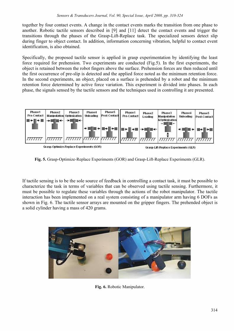
Sensors & Transducers Journal, Vol. 90, Special Issue, April 2008, pp. 310-324
314
together by four contact events. A change in the contact events marks the transition from one phase to another. Robotic tactile sensors described in [9] and [11] detect the contact events and trigger the transitions through the phases of the Grasp-Lift-Replace task. The specialized sensors detect slip during finger to object contact. In addition, information concerning vibration, helpful to contact event identification, is also obtained. Specifically, the proposed tactile sensor is applied in grasp experimentation by identifying the least force required for prehension. Two experiments are conducted (Fig.5). In the first experiments, the object is retained between the robot fingers above the surface. Prehension forces are then reduced until the first occurrence of pre-slip is detected and the applied force noted as the minimum retention force. In the second experiments, an object, placed on a surface is prehended by a robot and the minimum retention force determined by active force variation. This experiment is divided into phases. In each phase, the signals sensed by the tactile sensors and the techniques used in controlling it are presented.
Fig. 5. Grasp-Optimize-Replace Experiments (GOR) and Grasp-Lift-Replace Experiments (GLR).
If tactile sensing is to be the sole source of feedback in controlling a contact task, it must be possible to characterize the task in terms of variables that can be observed using tactile sensing. Furthermore, it must be possible to regulate these variables through the actions of the robot manipulator. The tactile interaction has been implemented on a real system consisting of a manipulator arm having 6 DOFs as shown in Fig. 6. The tactile sensor arrays are mounted on the gripper fingers. The prehended object is a solid cylinder having a mass of 420 grams.
Fig. 6. Robotic Manipulator.

Sensors & Transducers Journal, Vol. 90, Special Issue, April 2008, pp. 310-324
315
3. The Contact Model and Application Fluctuations in tactile data are observed within a time interval during which a sequence of stresses is cyclically applied to the specimen at the contact point. The stress waves are generally triangular, square, or sinusoidal, and the typical cycles of stress are reverse stresses, fluctuating stresses, and irregular or random stresses [12]. An understanding of the nature of physical contacts will aid in analyzing robotic prehension. When two objects come into contact, they will exert forces at the contact point. The z-axis is the axis parallel to the normal contact point n and normal forces are represented by nF . Contact friction forces perpendicular to the normal force are represented by tF . Contact friction forces on the x and y axes are represented by xF and yF , respectively. The relationship between contact friction forces and the normal force on the contact plane are represented in (1) below. 2222 ),( nyx FyxFF µ≤+ , (1) However, in this study the coefficient of friction ),( yxµ is a function of the coordinate system, which is different from Amantons’ friction law [13]. The surface contact between two objects results in a temporary elastic deformation, whose magnitude depends on the size of the applied force. Permanent, plastic deformations do not normally occur during robotic manipulation and will not be considered in this model. When the contact area is small, frictional forces on the surface are high, expanding the contact area due to its deformability. If the local direct stress vσ is set as a constant, the area receiving the pressure iN will be equal to vii NA σ/= . Thus, the total area under stress will be:
σσσσNNNNAAAA
v
i
vviT =++=+++= ...... 21
21 , (2)
where N represents the vector sum of all the normal forces. For hard objects, the actual contact area will be proportional to the magnitude of the force. However, the situation becomes more complicated with less rigid, compliant viscoelastic surfaces such as the polymer foams used in simple tactile sensors. However, in many cases the frictional forces involved in the viscoelastic deformation of polymeric materials have non-linear components which cannot be calculated using the above equations. In addition, the deformation does not only depend on the size of the normal force N but also on its direction and length, which in turn depends on the shape of the object in contact. If the deformation and the degree of force are held constant, then the contact area can be represented by the formula βN . As an illustration, for an elastic rubber-like solid 3/2=β [14], this is a general characteristic of most polymers. Howell’s equation [15] for frictional force can be reorganized as NKNF )( 1−= β , where )( 1−βKN is assumed to be equal to the coefficient of friction 0µ . This equation shows the complexity of the relationship between the normal force and the coefficient of friction 0µ , which consists of two variables. The effective coefficient of friction will reduce as the size of the exerted force increases. In other words, the compressive area has a lower coefficient of friction than the tensile area. The generation of roughness induced dynamic grasping at a deformable contact may be viewed most simply in the context of the model shown in Fig. 7. Qualitative models to describe the behaviour of a typical polymer will now be introduced. The Kelvin-Voigt model gives retarded elastic behaviour which represents a crosslinked polymer. The Maxwell model gives steady state creep typical of an uncured polymer. With the composition model as shown, it can describe both types of behaviour. The
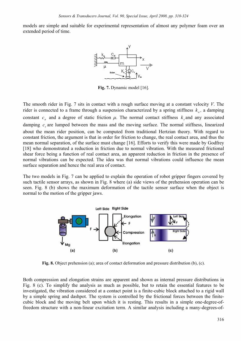
Sensors & Transducers Journal, Vol. 90, Special Issue, April 2008, pp. 310-324
316
models are simple and suitable for experimental representation of almost any polymer foam over an extended period of time.
Fig. 7. Dynamic model [16].
The smooth rider in Fig. 7 sits in contact with a rough surface moving at a constant velocity V. The rider is connected to a frame through a suspension characterized by a spring stiffness ak , a damping constant ac and a degree of static friction µ. The normal contact stiffness sk and any associated damping sc are lumped between the mass and the moving surface. The normal stiffness, linearized about the mean rider position, can be computed from traditional Hertzian theory. With regard to constant friction, the argument is that in order for friction to change, the real contact area, and thus the mean normal separation, of the surface must change [16]. Efforts to verify this were made by Godfrey [18] who demonstrated a reduction in friction due to normal vibration. With the measured frictional shear force being a function of real contact area, an apparent reduction in friction in the presence of normal vibrations can be expected. The idea was that normal vibrations could influence the mean surface separation and hence the real area of contact. The two models in Fig. 7 can be applied to explain the operation of robot gripper fingers covered by such tactile sensor arrays, as shown in Fig. 8 where (a) side views of the prehension operation can be seen. Fig. 8 (b) shows the maximum deformation of the tactile sensor surface when the object is normal to the motion of the gripper jaws.
Fig. 8. Object prehension (a); area of contact deformation and pressure distribution (b), (c).
Both compression and elongation strains are apparent and shown as internal pressure distributions in Fig. 8 (c). To simplify the analysis as much as possible, but to retain the essential features to be investigated, the vibration considered at a contact point is a finite-cubic block attached to a rigid wall by a simple spring and dashpot. The system is controlled by the frictional forces between the finite-cubic block and the moving belt upon which it is resting. This results in a simple one-degree-of-freedom structure with a non-linear excitation term. A similar analysis including a many-degrees-of-

Sensors & Transducers Journal, Vol. 90, Special Issue, April 2008, pp. 310-324
317
freedom model for the wheel vibration, yet using only simple models for the friction, has been performed by Heckl and Abrahams [19]. The governing second order equation for this system is: ),( xxFsxxrxm &&&&&& =++ , (3) where m is the mass of the finite-cubic block, s is the spring constant, and r is the damping coefficient. The frictional force is given by ),( xxF &&& , although it may be more natural to think of it as varying with time. 3.1. First Case: Grasp-Optimize-Replace The governing equations for the contact surface, obtained by summing forces on the rider mass are:
)()()()()()(tFyykyycymtFxxkxxcxm
Niesies
Gieaiea=−+−+=−+−+
&&&&
&&&&
)()( tFtF NDG µ= , (4)
where )(tFN is the fluctuating force normal to the tactile surface while )(tFG is the fluctuating frictional force. Anand [20] equates )(tFN to )(tFG using the reciprocal of Dµ as shown in (4). It is important to note that the deformation has a y component because some material passes underneath the contact which means that the sliding speed in x and the stain rate y, normal to the surface, are directly coupled [21]. Dieaieaiesies xxkxxcxmyykyycym µ/))()(()()( −+−+=−+−+ &&&&&&&& . When one of the contact points slips, the relationship between displacement and time will be approximated to a linear function [22]. In linear cases as mention by Howe [22], the slip displacement can be described as: Htx = , (5)
where H is slope of Fig. 9. Substituting x from (5) into the right hand side of (4) gives: Daaiesies HtkHcyykyycym µ/)()()( +=−+−+ &&&& . (6) The deformation surface between the object and tactile surfaces can be represented by 022 =− pyz , and from Howell’s definition [15] 1−= βµ KND , with 3/2=β and 1=K . Then, the minimized form is: )()()( 3/2 HtkHczyykyycym aaiesies +=−+−+ &&&& , and (7) BtAyykyycym iesies +=−+−+ )()( &&&& , (8) where HczA a
3/2= and HkzB a3/2= .
The solution to the differential equation 0=++ yyy &&& will be in the form: )()()( tytyty pc += . Solving the integral equation gives the solution of )(typ and )(tyc which becomes:

Sensors & Transducers Journal, Vol. 90, Special Issue, April 2008, pp. 310-324
318
32
32
)1()( HzktHzCty aap +−= and )23sin()
23cos()( 2
22
1 teCteCtytt
c
−−+= respectively.
In the case of a nonlinear or polynomial function, such as: dtbt ceaex += or pbtatx nn +++= − ...1 then the model nevertheless yields a single frequency solution. Pre-slip on some contact points (local slip) will appear before total slip occurs. This pre-slip can be detected by checking the oscillation frequency (fluctuation signal) and is identified as a pre-slip condition for the whole object. In the Grasp-Optimize-Replace experiment, the object was held between the robot gripper fingers. The robot would then decrease the prehension force until it could detect slip at some contact points which in turn would be indicative of complete slippage. The rule sets can be adapted by checking the oscillation frequency in the tactile array. If there exist some tactile elements having the same frequency of vibration, then whole pre-slip can be recognized.
Fig. 9. Slip displacement functions.
3.2. Second Case: Grasp-Lift-Replace In the second experiment, the deformation equation 022 =− pyz would not be correct any more because there exists an additional deformation of the contact surface when the robot tries to lift the object. Dundurs [23] presented the solution for the shear tractions, S(x) with dislocation distribution on an elastic material. He introduced geometry of the problem for elastic contacts as depicted in Fig. 10. The two components of force, shear force-P(t) and normal force-Q(t), can vary independently and are introduced as shear traction. The contact between objects is separated into three zones corresponding to point locations along the x -axis. He described the shear traction based on the location of points in the slip zone (a) and stick zone (b) when they are dislocated.
Fig. 10. Geometry of the problem by Dundurs [23].

Sensors & Transducers Journal, Vol. 90, Special Issue, April 2008, pp. 310-324
319
Point locations a and b along the x-axis at initial distributions will be moved to locations 1a and 1b when variations in )(tP and )(tQ along the x-axis occur. Shear traction along the x -axis will simply be a function of x . By defining a set of regime (rules), Dundurs presented the existence of shear traction fluctuations as shown in Fig. 11. From the conclusions made by Dundurs, this means there exists an extra term varying with time in the equations pertaining to surface deformation, i.e. )sin(at . Then the equation of surface deformation, for example, will be )sin(2/2 atpzy += . With Howell’s definition, the friction coefficient will
be 3 2 )sin(2// atpzKD +=µ or 3 )sin(/1 atDCD +=µ , where pzKC 2/23−= and 3−= KD . Equation (4) will become: )()sin()()( 3 HtkHcatDCyykyycym aaiesies ++=−+−+ &&&& . (9)
Fig. 11. Distributions of shear tractions for loading from (P1, Q1): (A)-Initial distribution; (B)-regime I; (C)-regime II (Regimes are defined by Dundurs [23]).
The same method can be used to find the solution to the differential equations, but )(typ will be different.
∫∫ +−= dtyyWtgyydt
yyWtgyytyp ),(
)(),(
)()(21
12
21
21
where )()sin()( 3 HtkHcatDCtg aa ++= ,
)23cos(2
11 teCyt
−= , )
23sin(2/
22 teCy t−= ,
and 22121 2
3),(t
eCCyyW−
= . Then, the solution will be
dtBtAatDCtetedtBtAatDCtetetytttt
p ∫ +++∫ ++−=−−
)()sin()23cos()
23sin(
32)()sin()
23sin()
23cos(
32)( 322322 (10)
It may not be necessary to find the integral solution because the solution, )(typ , will always contain the term “ )sin(at ”. That means in slippage situations, there is always more than one oscillation frequency

Sensors & Transducers Journal, Vol. 90, Special Issue, April 2008, pp. 310-324
320
(different numbers of fluctuation cycles) in the tactile array. One frequency is derived from the solution of )(tyc , another from the solution of )(typ . The alternating signals disperse throughout numerous tactile elements. When slip occurs, some of the elements give rise to signal changes. During prehension, the tactile sensor surface retracts in accordance to the object shape. Slip causing tangential force components affects only certain tactile elements. To rapidly measure the slip signal during prehension the computer memory may be organized in stacks. Locations T1, T2, ... Tn hold information from tactile sensors in the form of x-bar (average x-axis coordinate of force) and y-bar, vibrating cell, and vibration frequency. The subscript of T is the time of data collection - the number with the highest value in the stack being the most recent one. To compare stack data, indexes (pointers) called ‘index 1’ and ‘index 2’ are used to scan the data. Index 1 locates the starting point of the scan or the oldest stored data, whereas index 2 locates the finishing point of the scan or the current data. The data located by index 1 is compared with those located by index 2. Index 2 values are continually compared with Index 1 and decreased until the latest data is located. The location of index 1 is repeatedly scanned until index 2 locates the oldest stored data which means that the process is complete. For the first experiment, there are three conditions which successfully indicate pre-slip. The first one is the differences in vibrating tactile element location determined by different stack pointers. The second one is the equal frequency of vibration determined by different stack pointers. The last condition is that the first two conditions are simultaneously true for both sides of the gripper. For the second experiment, there are four conditions, which indicate pre-slip if they are true. The first one is the inequality in the x-bar and y-bar coordinates determined by both stack pointers. The second one is the differences in vibrating tactile element location determined by different stack pointers. The third one is the frequency of vibration as determined by higher stack pointers being larger than that determined by lower stack pointers. The final condition is that the first three conditions are simultaneously true on any of the fingers. 4. Analysis of Results The GOR experiment has been verified by the accelerometer chip to confirm the sensitivity of the proposed algorithm. As shown in Fig. 12, the accelerometer is attached on the surface of a grasped object. Whenever the grasped object slipped or moved from the gripper finger, the acceleration sensor would detect this. The output vibrations produced by an acceleration sensor and the display were then recorded while the robot decreased its grasping force. Overall, the response of the system was adequate for the purpose of testing the effectiveness of the proposed algorithm. The system is capable of logging the acceleration and it does this with a sample frequency of 200 Hz. The complete acceleration sensor is shown in Fig. 12 where the accelerometer is the small chip on the printed circuit board. The acceleration sensor, SCA3000 chip, is a three-axis accelerometer consisting of a 3D-MEMS sensing element. The sensor offers acceleration information via the SPI interface, and the measurement resolution is 0.75 2/ smm . The measured response amplitude was flat within ± 2 2/ sm across. There appeared to be severe mechanical vibrations or acceleration when the grasped object slipped from the finger gripper. In observing ten trials of experimental results, it can be confirmed that the proposed algorithm is faster and more sensitive than the acceleration sensor. Warning of a potential slip situation was between three and six force decrements prior to release of the grasped object from the gripper. By use of a voice synthesizer, the robot vocally warns of pre-slip and then continues decrementing the prehension force until object release. Impressive is the fact that, despite its sensitivity, the acceleration sensor first detects movement at the point of total slip.
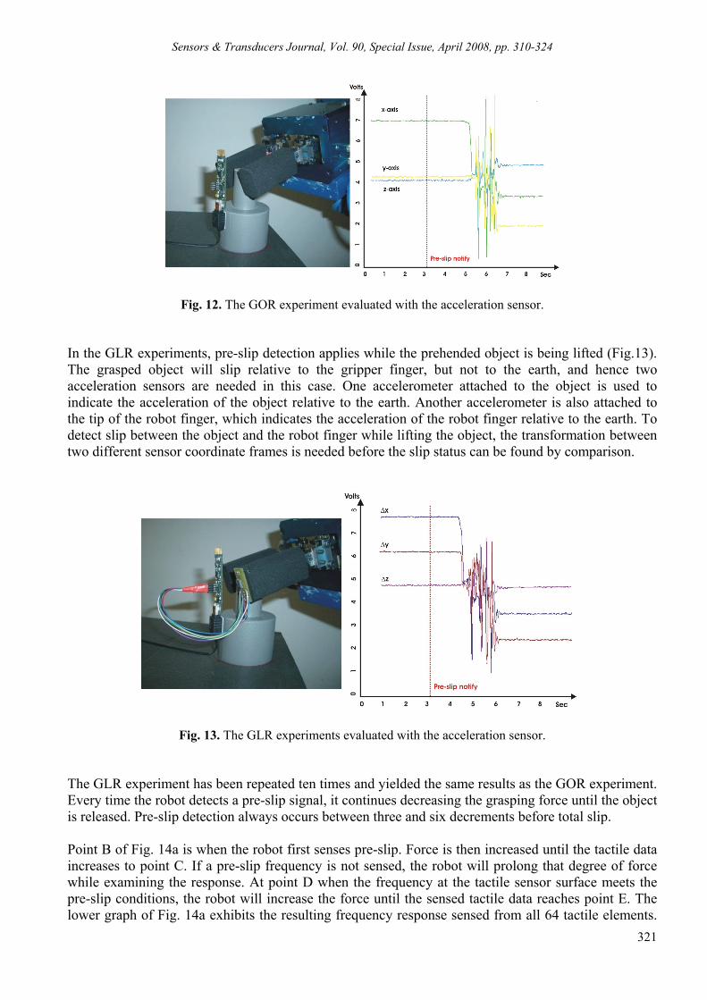
Sensors & Transducers Journal, Vol. 90, Special Issue, April 2008, pp. 310-324
321
Fig. 12. The GOR experiment evaluated with the acceleration sensor.
In the GLR experiments, pre-slip detection applies while the prehended object is being lifted (Fig.13). The grasped object will slip relative to the gripper finger, but not to the earth, and hence two acceleration sensors are needed in this case. One accelerometer attached to the object is used to indicate the acceleration of the object relative to the earth. Another accelerometer is also attached to the tip of the robot finger, which indicates the acceleration of the robot finger relative to the earth. To detect slip between the object and the robot finger while lifting the object, the transformation between two different sensor coordinate frames is needed before the slip status can be found by comparison.
Fig. 13. The GLR experiments evaluated with the acceleration sensor.
The GLR experiment has been repeated ten times and yielded the same results as the GOR experiment. Every time the robot detects a pre-slip signal, it continues decreasing the grasping force until the object is released. Pre-slip detection always occurs between three and six decrements before total slip. Point B of Fig. 14a is when the robot first senses pre-slip. Force is then increased until the tactile data increases to point C. If a pre-slip frequency is not sensed, the robot will prolong that degree of force while examining the response. At point D when the frequency at the tactile sensor surface meets the pre-slip conditions, the robot will increase the force until the sensed tactile data reaches point E. The lower graph of Fig. 14a exhibits the resulting frequency response sensed from all 64 tactile elements.

Sensors & Transducers Journal, Vol. 90, Special Issue, April 2008, pp. 310-324
322
The final decision as to whether pre-slip has occurred or not depends on analysis of the complete data. Points B, C, and D in Fig. 14 a are found to have pre-slip, and the least possible force needed to lift the object shown by the tactile sensors is approximately 150 (dimensionless ADC data). The second experimental results are illustrated in Fig. 14b. At the outset, the robot will use a predetermined force to grasp the object. When the inner surface of the grippers make contact with the object and the tactile data are approximately 90 (dimensionless ADC data) at point A, the robot will decrease the prehension force, i.e. by incrementally increasing the distance between the fingers. The tactile data will gradually decrease to point B, upon which the frequency response will be sensed and follow the conditions described in the lower graph of Fig. 14 b. The lower graph of Fig. 14 b exhibits the results of the frequency response sensed from all 64 tactile elements. To reach a decision as to whether a pre-slip condition has been reached or not requires another account as the sensed signals do not all result from pre-slip. For instance, they may result from the nature of the material used to develop the surface of the tactile sensors. Many tactile arrays are made from polymeric materials and many different types of foam are utilized. These have physical characteristic which differ enormously from those of rigid materials such as metals. Slow shape restoration results in unstable foam mass, causing the frequency response to fluctuate. Hence, the response does not result from pre-slip, but from the characteristics of the tactile sensor surface material. From the behavior of the localized contacts between tactile sensor and object surfaces, the minimum force cannot be determined by a unidirectional increase or decrease in applied force.
Fig. 14. Minimum prehension force determined by increasing and decreasing applied force.
This means the same degree of force exerted at different times will result in different prehension stabilities. To exemplify, at a certain point in time the force at point E lies between that at point A and C and is adequate for object prehension without pre-slip. The force required to retain the object now must be equal to or greater than that at point E.

Sensors & Transducers Journal, Vol. 90, Special Issue, April 2008, pp. 310-324
323
5. Conclusions Tactile sensing elements can acquire force feedback information at the contact points between a grasped objects and the tactile surface. The tactile sensor is capable of measuring near static acceleration which is interesting to investigate. A proposed method for calibrating the tactile data to predict slip is extremely useful. The advantage of this method is that the acquisition of direct contact forces provides grasping force adaptability in addition to optimum prehension by determining the necessary minimum applied force. With respect to real applications, the manipulation of fragile components or assemblies requires precise force control under conditions of varying acceleration. The force feedback information from the tactile surfaces used in this work can be used to optimize gripper alignment and achieve object prehension and manipulation with using minimum retention force. This procedure can be restructured in such a way that the orientation of an object, with respect to a gripper, can be determined regardless of its identity. Minimum prehention forces are ascertained with respect to its desired stable orientation. However, where objects of differing size and geometry are used, a different scanning speed may be necessary. For examples, heavier objects need the shorter processing loop times in order to adjust the minimum force. Comprehensive details about the prototype sensor, data acquisition and processing principles together with incorporated mathematical derivations for part pre-slip sensing are provided in a previously published work [24]. References [1]. D. P. J. Cotton, A. Cranny, N. M. White, P. H. Chappell and S. P. Beeby, A Novel Thick-Film
Piezoelectric Slip Sensor for a Prosthetic Hand, IEEE Sensors Journal, 7, 5, 2007, pp. 752-761. [2]. D. S. Childress, Historical aspects of powered limb prosthesis, Clinical Prosthetics and Orthotics, 9, 1985,
pp. 2-13. [3]. Y. Yamada, Hiroyuki Morita, and Yoji Umetani, Slip phase isolating: impulsive signal generating
vibrotactile sensor and its application to real-time object regrip control, Robotica, 18, 1, 2000, pp. 43-49. [4]. C. Melchiorri, Slip detection and control using tactile and force sensors, Mechatronics, IEEE/ASME
Transactions, 5, 3, 2000, pp. 235–243. [5]. Schunk GmbH & Co, catalogue “SCHUNK_Automation_Modulare_Robotik_DE_EN. pdf”, available at:
http://www.schunk.com/schunk/index.html [6]. R. S. Johansson and G. Westling, Roles of glabrous skin receptors and sensorimotor memory in automatic
control of precision grip when lifting rougher and more slippery objects, Exp. Brain Res., 56, 1984, pp. 550-564.
[7]. G. Westling and R. S. Johansson, Factors influencing the force control during precision grip, Exp. Brain Res., 53, 1984, pp. 277-284.
[8]. G. Cadoret and A. M. Smith, Friction, not texture, dictates grip forces used during object manipulation, Journal Neurophysiol, 75, 1996, pp. 1963-1969.
[9]. R. D. Howe and M. R. Cutkosky, Sensing Skin Acceleration of Slip and Texture Perception. IEEE International Conference on Robotics and Automation, 1989, p. 145-150.
[10]. R. D. Howe and M. R. Cutkosky, Practical force-motion models for sliding manipulation, International Journal of Robotics Research, 15, 6, 1996, pp. 557–572.
[11]. R. D. Howe and M . R. Cutkosky, Dynamic Tactile Sensing: Perception of Fine Surface Features with Stress Rate Sensing, IEEE Trans on Robotics and Automation, 9, 2, 1993, pp. 140-151.
[12]. G. E. Dieter, Metalurgia Mecânica, Mc Graw Hill Inc. 1981. [13]. D. Dowson, History of Tribology, Longman Inc., New York, 1979. [14]. B. Lincoln Br. J., Frictional and elastic properties of high polymeric materials, Apply Physics, 3, 1952,
pp. 260-263. [15]. H. G. Howell and J. Mazur, Amontons’ Law and Fibre Friction, Journal of the Textile Institute, 1953,
pp. 59-69. [16]. A. Krawietz, Materialtheorie, Mathematische Beschreibung des phdnomenologischen thermomechanischen
Verhaltens, Springer-Verlag, Berlin, 1986.

Sensors & Transducers Journal, Vol. 90, Special Issue, April 2008, pp. 310-324
324
[17]. R. A. Ibrahim, Friction-induced vibration, chatter, squeal, and chaos: Part i-mechanics of contact and friction, Applied Mechanics Reviews, 47, 1994, pp. 209-226.
[18]. D. Godfrey, Vibration reduced metal-to-metal contact and causes an apparent reduction in friction, ASLE Transactions, 10, 1967, pp. 183-192.
[19]. M. A. Heckl and I. D. Abrahams, Active control of friction-driven oscillations, Journal of Sound and Vibration, 193, 1996, pp. 417-426.
[20]. A. Anand and A. Soom, Roughness-Induced Transient Loading at Sliding Contact During Start-Up, Journal of Tribology, 106, 1984, pp. 49-53.
[21]. W. P. Vellinga and C. P. Hendrinks, Sliding friction dynamics of hard single asperities on soft substrates, Physic Review, 63, 2001, pp. 12-14.
[22]. R. D. Howe and M. R. Cutkosky, Sensing Skin Acceleration of Slip and Texture Perception, IEEE International Conference on Robotics and Automation, 1989, pp. 145-150.
[23]. J. Dundurs and M. Comninou, An Education Elasticity Problem With Friction, Part3: General Load Paths, Journal of Applied Mechanics, 50, 1983, pp. 77-84.
[24]. S. Petchartee, G. Monkman, Slip Prediction through Tactile Sensing. In: Proc. 2007 International Conference on Sensing Technology, New Zealand, 2007.
___________________
2008 Copyright ©, International Frequency Sensor Association (IFSA). All rights reserved. (http://www.sensorsportal.com)

Sensors & Transducers Journal, Vol. 90, Special Issue, April 2008, pp. 325-332
325
Sensors & Transducers
ISSN 1726-5479© 2008 by IFSA
http://www.sensorsportal.com
Broadband and Improved Radiation Characteristics of Aperture-Coupled Stacked Microstrip Antenna
for Mobile Communications
Sajal Kumar PALIT School of Engineering and Advanced Technology,
Massey University, Wellington, New Zealand E-mail: [email protected]
Received: 15 October 2007 /Accepted: 20 February 2008 /Published: 15 April 2008 Abstract: A new broadband microstrip antenna has been reported in this paper. A significant breakthrough in bandwidth enhancement has been achieved by optimizing the antenna’s dimensions, substrate materials, substrate thickness, aperture dimensions and by positioning a thin conductor at a particular angle as a reflector to stop the back radiation. The measured ultra-bandwidth has been found to be 73% at VSWR = 2.0 at 850 MHz. The gain of the modified microstrip antenna has also improved from 8.6 dB to 9.2 dB. It is found that the back radiation has reduced significantly due to the conducting plane inserted below the microstrip feed line. The front-to-back ratio has improved from 12 dB to 20 dB. This antenna can find useful applications in wireless communications. Copyright © 2008 IFSA. Keywords: Microstrip antenna, Broadband, Stacked patch, Substrate, Aperture-coupled 1. Introduction Although microstrip antennas have the advantages of low-profile, conformal, small size, low weight, low production cost and high design flexibility, its narrow bandwidth characteristic seriously limits its application. Microstrip antennas also have some other limitations such as: lower gain; lower power handling capability; excitation of surface waves; poor cross-polarization, radiation from feeds, and junctions etc.

Sensors & Transducers Journal, Vol. 90, Special Issue, April 2008, pp. 325-332
326
Significant research has been pursued during the last two decades to increase the bandwidth [1-12] of the microstrip antennas. Design of broadband and dualband microstrip antennas were studied by Palit et al [1-6]. It is found that a properly designed notched microstrip patch can exhibit wideband and dualband operations. The two resonant frequencies are probably the results of the coupling between the main patch and the notch resonant frequencies. The maximum impedance bandwidths of 38 % for band 1 and 27 % for band 2 were achieved for coax-fed single notched patch. Palit et al [6] described a composite patch antenna to enhance bandwidth by adding a patch on top of the primary patch and another patch as a director in the right radiating side of the top one. It is found that the bandwidth is very sensitive to the gap between the main patch and the parasitic patch. The feed location is very important for good matching, which increases the bandwidth. This paper presents a broadband aperture fed stacked patch antenna. The notable features of this feed configuration are wider bandwidth and the shielding of the radiation patch from the feed structure. Aperture-coupled microstrip feed uses two substrates separated by a common ground plane. The slot can be of any shape and size and these parameters are used to improve the bandwidth. The radiation of the open end of the feed line does not interfere with the radiation pattern of the patch because of the shielding effect of the ground plane. This also improves the polarization purity. This paper shows a very significant bandwidth enhancement achieved (73 %) by adding a reflector at the bottom of the aperture coupled stacked microstrip antenna. It also enhanced the front-to-back ratio of the radiation level and gain of the designed antenna. 2. Aperture Coupled Stacked Patch Antenna Design Fig. 1 shows the schematic diagram of the designed aperture coupled stacked patch antenna.
Fig. 1. Aperture coupled stacked microstrip antenna. The size of the lower patch is different from that of the upper patch to obtain a slightly different resonant frequency. Various parameters such as substrate thicknesses d1 and d2, dielectric constants εr1 and εr2, patch sizes and feed location were adjusted to optimize the bandwidth. The stacked patch configuration has been designed and analyzed using Ensemble - a software package based on method of moment and the lossy transmission line model. Fig. 1 shows our designed antenna having two resonant patches that are different in size, with the lower patch fed by a microstrip line through a

Sensors & Transducers Journal, Vol. 90, Special Issue, April 2008, pp. 325-332
327
resonant slot in the common ground plane. The basic feature of this structure is that each of the three resonators (two patches and the slot) has its own impedance loop. There are also mutual couplings among these resonances. The resonator parameters are adjusted to bring the impedance loops closer to each other. The substrate thickness and the dielectric constant between the resonators are also varied to adjust the mutual coupling between them resulting in a wider bandwidth. Fig. 2 shows the experimental set up for measuring the impedance bandwidth of the designed microstrip antenna. Voltage Standing Wave Ratio (VSWR) and return loss (dB) as a function of frequency and impedance loops as functions of substrate thickness were measured using network analyzer. Some of the measured results are compared with the simulated ones to validate the design.
Fig. 2. Experimental set-up for measuring VSWR as a function of frequency. In this design, two dielectric substrate layers and one foam layer were stacked together. The first layer supports the microstrip feed line on one side, and the ground plane with a coupling aperture on the other [Fig. 1]. On the second layer, the rectangular patch was etched on one side and the conducting layer (copper) was removed from the other side. The foam layer is used to reduce the dielectric constant and increase the thickness of the substrate for wider bandwidth. It is difficult to etch the patch directly on the foam because of its porosity. A thin perspex layer is used to support the second patch whose dimension is different than the first patch so as to obtain different resonant frequency. The antenna input impedance is matched to 50 Ω using a microstrip quarter wave matching which was etched on the same side as the microstrip feed line. The dimensions of the patches and the slots were optimized using the Ensemble software package. The software is based on the full-wave method to solve a mixed-potential integral equation which takes into consideration the effects of discontinuities, surface waves and spurious radiations. Figs. 3-6 show the changes in input impedance as functions of antenna parameters. It is found that change of the lower patch size is very critical which contributes to both mutual resonances with the aperture below and the upper patch and therefore affects the size of both the loops as found in the Figs. 3-6. There is only one inductive loop since the air gap (d2 = 30 mm) is too large for mutual coupling between the patches.

Sensors & Transducers Journal, Vol. 90, Special Issue, April 2008, pp. 325-332
328
Fig. 3. SL = 118.5 mm, SW = 5.0 mm, Lstub = 20.0 mm, εrf = 4.4, df = 1.6 mm, εr1 = 2.54, d1 = 40.0 mm, εr2 = 1.0, d2 = 30.0 mm, εr3 = 2.54, d3 = 30.0 mm PL1 = 88.6 mm, PW1 = 88.6 mm, PL2 = 167.6 mm, and PW2 = 167.6 mm.
Fig. 4. SL = 98.6 mm, SW = 5.0 mm, Lstub = 20.0 mm, εrf = 4.4, df = 1.6 mm, εr1 = 2.54, d1 = 10.0 mm, εr2 = 1.0, d2 = 5.0 mm, εr3 = 2.54, d3 = 30.0 mm PL1 = 97.6 mm, PW1 = 118.6 mm, PL2 = 97.6 mm, and PW2 = 117.6 mm.
Fig. 5. SL = 98.6 mm, SW = 5.0 mm, Lstub = 20.0 mm, εrf = 4.4, df = 1.6 mm, εr1 = 2.54, d1 = 20.0 mm, εr2 = 1.0, d2 = 10.0 mm, εr3 = 2.54, d3 = 30.0 mm PL1 = 97.6 mm, PW1 = 108.6 mm, PL2 = 97.6 mm, and PW2 = 132.6 mm.
The loops are slowly coming closer and getting tightly coupled as the substrate thickness d1 and d2 have been reduced.
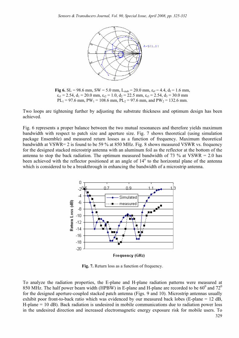
Sensors & Transducers Journal, Vol. 90, Special Issue, April 2008, pp. 325-332
329
Fig 6. SL = 98.6 mm, SW = 5.0 mm, Lstub = 20.0 mm, εrf = 4.4, df = 1.6 mm, εr1 = 2.54, d1 = 20.0 mm, εr2 = 1.0, d2 = 22.5 mm, εr3 = 2.54, d3 = 30.0 mm PL1 = 97.6 mm, PW1 = 108.6 mm, PL2 = 97.6 mm, and PW2 = 132.6 mm.
Two loops are tightening further by adjusting the substrate thickness and optimum design has been achieved. Fig. 6 represents a proper balance between the two mutual resonances and therefore yields maximum bandwidth with respect to patch size and aperture size. Fig. 7 shows theoretical (using simulation package Ensemble) and measured return losses as a function of frequency. Maximum theoretical bandwidth at VSWR= 2 is found to be 59 % at 850 MHz. Fig. 8 shows measured VSWR vs. frequency for the designed stacked microstrip antenna with an aluminum foil as the reflector at the bottom of the antenna to stop the back radiation. The optimum measured bandwidth of 73 % at VSWR = 2.0 has been achieved with the reflector positioned at an angle of 14o to the horizontal plane of the antenna which is considered to be a breakthrough in enhancing the bandwidth of a microstrip antenna.
Fig. 7. Return loss as a function of frequency.
To analyze the radiation properties, the E-plane and H-plane radiation patterns were measured at 850 MHz. The half power beam width (HPBW) in E-plane and H-plane are recorded to be 600 and 720 for the designed aperture-coupled stacked patch antenna (Figs. 9 and 10). Microstrip antennas usually exhibit poor front-to-back ratio which was evidenced by our measured back lobes (E-plane = 12 dB, H-plane = 10 dB). Back radiation is undesired in mobile communications due to radiation power loss in the undesired direction and increased electromagnetic energy exposure risk for mobile users. To

Sensors & Transducers Journal, Vol. 90, Special Issue, April 2008, pp. 325-332
330
improve the front-to-back ratio a thin aluminum foil was used as a reflector and the result was very encouraging. The measured E and H planes radiation patterns for the modified antenna with a reflector are also shown in the Figs. 9 and 10 for comparison. It is found that the front-to-back ratios for both E and H planes have improved significantly. It is also found that the gain of the antenna with a reflector has also improved from 8.8 dB to 9.2 dB.
Fig. 8. Measured VSWR as a function of frequency.
(a)
(b)
Fig. 9. Measured E-plane radiation patterns of the aperture-coupled stacked patch antenna without a reflector (b) with a reflector.

Sensors & Transducers Journal, Vol. 90, Special Issue, April 2008, pp. 325-332
331
(a)
(b)
Fig. 10. Measured H-plane radiation patterns of the aperture-coupled stacked patch antenna (a) without a reflector (b) with a reflector.
3. Analysis of the Results In this paper an aperture-coupled stacked microstrip antenna for mobile communications is studied. The purpose of the study is to increase the bandwidth, gain and improve the front-to-back radiation level for wireless communications. The aperture-coupled technique was initially proposed by Pozar [7, 11]. The technique consists of coupling energy from the microstrip feed line through a slot in the ground plane to the patch. The patch is isolated from the feed structure by the ground plane which reduces spurious radiation, and offers the designer the opportunity to choose different substrate materials for the feed and the radiating element. It is found that by choosing low dielectric constant substrate materials impedance bandwidth can be increased. In this design foam is used and the reflector is suspended which optimized the bandwidth. Substrate thickness also changes the bandwidth. The study found that thicker substrate offers wider bandwidth but reduces gain due to less coupling for a given aperture size. Patch length determines the resonant frequency and its width the resistance at resonance. Thinner feed substrate yields less spurious radiation from the feed line but yields higher losses due to increased resistivity. The length and the width of the coupling slot determine the coupling and back radiation. The width of the microstrip feed line and the placement control the input impedance of the antenna. 4. Conclusions The design and analysis of an aperture coupled stacked microstrip antenna have been made and reported in this paper. A significant breakthrough in bandwidth enhancement has been achieved by optimizing the antenna’s dimensions, substrate materials and thickness, aperture dimensions and by positioning an aluminum foil at a particular angle as a reflector to reduce the back radiation. The measured ultra-bandwidth is found to be 73 % at VSWR = 2.0 at 850 MHz. The front-to-back ratio of the radiation in both E and H planes and gain are found to have improved significantly. This antenna can find useful application for base station and in-building mobile network coverage for CDMA and GSM frequencies.

Sensors & Transducers Journal, Vol. 90, Special Issue, April 2008, pp. 325-332
332
References [1]. S. K. Palit, A New Ultra Broadband Microstrip Antenna for Wireless Communications, International
Conference on Sensing Technology (ICST 2007), Massey University, Palmerston North, New Zealand, 26-28 November 2007.
[2]. S. K. Palit and A. Hamadi, Design and development of wideband and dualband microstrip antennas, IEE Proceedings on Microwaves, Antennas and Propagation, Vol. 146, No. 1, February 1999, pp. 35-39.
[3]. S. K. Palit, A. Hamadi and D. Tan, Design of a wideband dual-frequency notched microstrip antenna, Proc. of IEEE Antennas and Propagation Society International Symposium, June 1998, Vol. 4, pp. 2351-2354.
[4]. S. K. Palit, A. Hamadi and J. P. Rayner, A new broadband slot coupled notch microstrip antenna, Proc. of IEEE AP/URSI Symposium, Baltimore, Maryland, USA, July 1996, p. 65.
[5]. S. K. Palit and A. Hamadi, A dual-band notch microstrip antenna for mobile communications, Asia-Pacific Microwave Conference Proceedings, New Delhi, Dec. 1996, Vol. 1, pp. 299-302.
[6]. S. K. Palit and N. Vijoyasinghe, Broadband microstrip antenna design, Chinese Journal of Radio Science, 1995, pp. 670-673.
[7]. D. M. Pozar and D. H. Schauberr, The analysis and design of microstrip antennas and arrays, IEEE Press, New York, 1996.
[8]. I. Park and R. Mitra, Aperture-coupled quarter-wave microstrip antenna, IEEE Antennas and Propagation Society International Symposium, Baltimore, USA, July 1996, Vol. 1, pp. 14-17.
[9]. R. Hill, A practical guide to the design of microstrip antenna arrays, Microwave Journal, February 2001, pp. 166-180.
[10]. R. Garg, P. Bhartia, I. Bahl, A. Ittipiboon, Microstrip antenna design handbook, Artech House, 2001, pp. 539-590.
[11]. S. D. Targonski, R. B. Waterhouse and D. M. Pozar, Design of wideband aperture stacked patch microstrip antenna, IEEE Trans Antennas and Propagation, Vol. AP-46, 1998, pp. 1245-1251.
[12]. K. L. Wong, C. L. Tang, J. Y. Chiou, Broadband Probe-Fed Patch Antenna with a W-shaped Ground Plane, IEEE Trans Antennas and Propagation, Vol. 50, No. 6, June 2002, pp. 827-831.
___________________
2008 Copyright ©, International Frequency Sensor Association (IFSA). All rights reserved. (http://www.sensorsportal.com)

Sensors & Transducers Journal, Vol. 90, Special Issue, April 2008, pp. 333-341
333
SSSeeennnsssooorrrsss &&& TTTrrraaannnsssddduuuccceeerrrsss
ISSN 1726-5479© 2008 by IFSA
http://www.sensorsportal.com
The Use of Bragg Gratings in the Core and Cladding of Optical Fibres for Accurate Strain Sensing
Ian G. PLATT and Ian M. WOODHEAD
Lincoln Ventures, PO Box 133, Lincoln, Christchurch 7640, New Zealand,
Tel.: +64 3 325 3748, fax: +64 3 325 3725 E-mail: [email protected], http://www.lvl.co.nz
Received: 15 October 2007 /Accepted: 20 February 2008 /Published: 15 April 2008 Abstract: Optical Fibre Sensors (OFS) have many advantages over others type of sensors for measuring strain or micro-displacement. This paper introduces a new configuration of Bragg gratings within an optical fibre to improve strain measurement resolution and accuracy. We describe the geometry, together with the research direction currently being undertaken to produce a commercially viable micro-displacement sensor suitable for a number of architectural and engineering application. Copyright © 2008 IFSA. Keywords: Optical fibre, Strain, Bragg, Micro-displacement 1. Introduction The ability to perform distributed strain measurements over a structural beam is of considerable importance in assessing both the safety and maintenance requirements of most civil engineering structures. There is an increasing awareness that efficient Structural Health Monitoring (SHM) can substantially decrease the maintenance expenditures of many structures and alleviate delays caused by unnecessary or unexpected repairs. As an example of this, the structural health monitoring of bridges has become a significant issue over the last decade. In the United States alone there are some 591,707 major bridges, nearly a third of which are classified as deficient or functionally obsolete [1]. The annual budget for maintenance is around US$4 billion, though it is estimated that approximately US$13.5 billion annually is required to repair and maintain all bridges to an acceptable level. This huge expenditure has placed considerable pressure on administrative bodies to put into place advanced bridge management programs, including real time structural monitoring and assessment instrumentation [2].

Sensors & Transducers Journal, Vol. 90, Special Issue, April 2008, pp. 333-341
334
The importance of SHM has attracted the attention of those working in the emerging field of Optical Fibre Sensors (OFS) and many advances have been made in techniques to enable such measurements (e.g. [3]). Much of this interest has been prompted by the relative inertness of optical fibres to environmental factors (e.g. moisture) and their low interference to the beam’s structural integrity (i.e. small cross section) making them ideal candidates for the desired distributed measurement process. Strain and loading measurements most often use devices firmly fixed to the sample to measure its micro-displacements under the action of some force. Bragg gratings etched within optical fibres do this by indicating the change in grating spacing as the fibre is stretched along with the sample (e.g. [4]). The practical application of such technology however has a number of drawbacks, including; 1) the response due to increased grating spacing is similar to that imposed by changes in temperature so the two effects are difficult to resolve, 2) fixing the fibre within or on the sample so that the fibre actually measures its true displacement is also difficult (while maintaining its major advantage of having a small cross section), 3) the strain induced deformation of along the fibre is not uniform and this effect is difficult to allow for [5]. It is the purpose of this paper to outline work currently under way to develop a robust and commercially viable Bragg grating strain sensor that can be used in a variety of measurement scenarios, while mitigating some of the major disadvantages. 2. Bragg Sensors Bragg grating technology is one of the most popular choices for OFS strain measurement sensors due to their simple manufacture (direct etching in the fibre core) and relatively strong reflected signal strength. Other OFS types, such as Fabry-Perot interferometers, are less popular since signal detection and resolution can be problematic requiring expensive equipment and specialist operators. Fig. 1 shows the typical arrangement used in current strain (micro-displacement) sensors. When a force is applied to the ends of the fibre sensor, the Bragg line spacing is increased and this results in a frequency shift of the backscattered peak.
Frequenc y
Amplitude
Frequenc y shift between inc ident (laser sourc e) and reflected signal is proportional stra in + tem perature
Core
Cladding
FF
Bragg Grating
Fig. 1. Basic concept behind a Bragg grating strain sensor. The frequency of the Bragg scattered component within an optical pulse is given by: 2B Gnλ λ= , (1)

Sensors & Transducers Journal, Vol. 90, Special Issue, April 2008, pp. 333-341
335
where λB is the scattered Bragg wavelength, λG is the grating wavelength and n is the refractive index of the fibre core. The change in the Bragg wavelength (δλB) is given by [6]:
( )( )2
12 11 1212
12B G
Tdnn n dTn P P Pυ δδε αδλ λ
⎡ ⎤⎛ ⎞ ⎛ ⎞⎢ ⎥= − − + + +⎜ ⎟ ⎜ ⎟⎜ ⎟⎢ ⎥⎝ ⎠⎝ ⎠⎣ ⎦
, (2)
where: P11 and P12 are components of the fibre strain tensor; δε is the applied longitudinal strain; ν is Poisson’s ratio; α is the coefficient of thermal expansion and T is the temperature. So a spectral shift is also generated by changes in the fibre temperature with the overall shift being a combination of the two effects. The coefficient of thermal expansion, α is very small and for silica fibre: ( )( )
2
12 11 12 0.222n
P P Pυ− + ≈
so that equation (2) becomes: 12 0.78B G
dnn Tn dT
δλ λ δε δ⎡ ⎤⎢ ⎥⎣ ⎦
= + (3)
In practice it is difficult to resolve the δε and δT component contributions of the spectral peak shift, δλB. Attempts have been made to combine two fibres, one under strain while a neighbouring one is shielded from the strain, in an effort to calibrate the temperature response. This approach works to some degree, but that fact that two fibres have to be excited in exactly the same manner for the small differences to be measured, means that a considerable degree of accuracy in relative fibre placement and detector sophistication is required. Other methods using several wavelength gratings and/or fibre dispersion properties have met with even less success, again because of the small differences involved. As well as temperature effects, other practical considerations need to be addressed when constructing a Bragg grating OFS. Table 1 lists some of these. Here interrogation techniques (including multiplexing) are not included, with the focus being upon the accuracy and reliability of the sensor itself.
Table 1. Some of the major problems facing the use of Bragg gratings in strain measurement sensors. Sensitive to a Temperature
The Bragg grating response will also be dependent on temperature. It is difficult to unwrap this from strain and this is the major inaccuracy involved.
Localized effects Localized “pinching” around the grating will cause it to be distorted and thus give a false indication of the distributed strain (i.e. strain over some longer length)
Bonding to the sub stratum
To measure strain the fibre jacket needs to be firmly bonded to the material. In external placements particularly, the small amount of movement to be measured may reside in fixings and glue etc. and not the fibre.
Small dynamic range
The range of measurable strain is quite small (from zero to about 1000 µstrain – 2000 µstrain) so peak detection and thus resolution are critical.

Sensors & Transducers Journal, Vol. 90, Special Issue, April 2008, pp. 333-341
336
3. Dual Bragg Gratings When considering a reconfiguration of the Bragg grating system to achieve optimal measurement performance some important points are worth noting: • Strain is given by ∆L/L where L is the original length and ∆L is the change in length due to stress. Thus to measure strain requires only the measurement of change in distance between allotted points. • Bragg diffraction can be induced by inscribed lines in either the core or cladding of the fibre. • The temperature sensitivity of the fibre is mostly (95%) due to the change in refractive index with temperature. A similar percentage change will occur within both the core and cladding material. Since a proportion of the bound mode travels parallel to the core axis within the cladding material via evanescent propagation (and this can be increased by a variety of methods), a grating within this region may also act as a good scatterer. By mechanically detaching the cladding from the core so that each is free to move independently two sets of adjacent gratings may be constructed (Fig. 2).
Fig. 2. Dual Bragg Gratings in core and cladding. The figure below shows a possible arrangement of cladding gratings to take advantage of a vernier geometry.
The optical properties between the two can be strictly maintained by applying liquid resins that are commonly used for other fibre optic matching purposes. Such a fibre, with Bragg gratings etched on both the core and cladding sections, will allow two new geometries to be exploited for micro measurement: 1. The cladding is under stress while the core is not. This means that both Bragg gratings will be under the same temperature and optical conditions, but with only one under stress. The current problems of providing a reference identical to the measurement sensor will be mitigated by this application. 2. Neither the core nor cladding is under stress, so that the Bragg gratings do not measure the micro shift by an increased grating spacing. Instead the relative displacement of the two is measured by a
Sensors & Transducers Journal, Vol. 90, Special Issue, April 2008, pp. 333-341
337
adopting a Vernier scale. This method unwraps strain from temperature, but also has the added advantage that when fixing the sensor to the sample, no allowance has to be made for stress within the fittings; the sensor becomes a purely stress free measurer of micro-displacement. The change in grating spacing is thus solely due to temperature variation. This also overcomes the relatively limited strain range of the OFS. These two approaches have a common starting point, the detachment of the core-cladding interface, and a significant part of future research will be devoted to this phase. Of the two methods the detached Vernier geometry, while being the most difficult to realize, offers the greatest advantage for a strain sensor. Such a system can solve (or at least alleviate) most of the technical difficulties highlighted in Table 1. As a rough, but reasonable guide, equation (3) may be rearranged to give for constant strain: 12
B GTdnn
n dTδδλ λ ⎛ ⎞= ⎜ ⎟
⎝ ⎠, (4)
giving: 61 6.67 101B
B
CT
dnn dTδ
δλλ
−= = × o , (5)
The numerical value assigned to equation (5) is given by [6] and [7]. If n is taken as the core refractive index and dn/dT is considered the same for the two media then it can be shown that the effect of temperature in grating separation between the core and cladding is around 10-14 oC, well below the expected system response of about 10-9. Since the strain is a measure only of the change in length there is no need for the fibre to be stretched in the manner of conventional techniques. This means that it is possible to shield the fibre from localized effects without effecting the strain measurement (see Fig. 3). The same argument leads to a reduction in the effect any bonding material may have in the measurement of actual strain as well as those problems caused by the non-homogeneous longitudinal strain field. There are also some practical limitations on the type of optical fibre that can be used in the dual Bragg grating sensor as specified here and in [8]. If the sensor is indeed realized by the detachment of the core and cladding a simple step refractive index profile will need to be used. The normalized frequency, V, for a circular waveguide is given by: ( )1/ 22 22
clV n nπ ρλ
= − , (6)
where: ρ is the diameter of the core; λ is the propagation wavelength; ncl is refractive index of the cladding. For single mode operation it can be shown (e.g. [9]) that V < 2.405. The amount of power flowing in the core can be estimated by the Mode Field Diameter (MDF) and this is a function of V and the core radius ρ. For V = 2 the MDF can be used to show [6] that approximately 85% of power flows within the core (15% in the cladding) and this core value increases quickly as V becomes larger. The power propagating within the cladding must be sufficient for reflection discrimination and so requires V < 2.

Sensors & Transducers Journal, Vol. 90, Special Issue, April 2008, pp. 333-341
338
This limits the fibre waveguide to single mode propagation, with a small normalized index difference, ∆, (see equation (8)) and small core radius (around 10 µm). To provide the maximum number of combinations, the cladding gratings will need to be distributed in annular sections radially around the core. The number of possible sections will depend upon the resultant reflection amplitudes of constructive and destructive interference over the active region. This together with the minimum number of aligned etched lines and proportion of power that can be injected into cladding modes required for detectable scattering will need to be modelled carefully in the early stages. The modelling component should be a relatively straight forward process, but constructing the physical system will of course present many optical engineering constraints including all those usually associated with optical systems such as diffraction and etendue etc. as well as some unique to fibre propagation such as mode coupling.
Fibre AnchorCladding Anchor(with detached Cladding)
Grating Vernier
Cladding Gap
Fig. 3. Proposed housing for the Vernier geometry type sensor.
4. Current Research Current work in constructing the two types of sensors described in the last section is focused upon mitigating against a number of operational problems, both observed and perceived. The most obvious difficulty to be solved is the detachment of the core from the cladding in a way that allows independent movement without compromising the integrity of the waveguide performance. It is likely that lubricants of the correct refractive index exist that can be used for this purpose, though other solutions or mitigating procedures also need to be explored. From equation (1) it can be seen that the refractive index of the medium will effect the Bragg spectral response. Typical step refractive index fibres have a normalized index difference (∆) between 0.003 – 0.01. So using the lower limit: 2 2
22co cl
co
n nn−
∆ = , (8)
0.0997cl conn = , (9) Using equation (1) for constant λG and a 1300 nm laser source gives the change in the Bragg reflected wavelength between the core and cladding of:

Sensors & Transducers Journal, Vol. 90, Special Issue, April 2008, pp. 333-341
339
92.6 10
BB co
co
m
nnλδλ δ=
= −×
, (10)
where δnco = 0.003. From equation (3) the Bragg wavelength shift due to a strain of 1000 µstrain (i.e. ∆L/L = 0.1%), at constant temperature is around 1X 10⁻⁹ m. Clearly, even at the lowest values of ∆ the impact of the different refractive indices is significant when considering the Vernier construction and this will need to be compensated for. One way of achieving this could be by creating different wavelength gratings λG, for the opposing Vernier components; though the required resolution may be difficult to achieve. Also challenging is the 3-Dimensional alignment of the gratings to provide adequate precision and coverage and will take some skill and undoubtedly increase the length of the fibre over which a single measurement can be taken. For both geometries, mode coupling of the forward propagating paths is likely to be strong when a grating mismatch occurs (i.e. when the gratings are not aligned). This means that incorporation of more than one sensor per length of fibre may require different wavelength regimes, something already experimented with by others. Since not all of the fibre cladding will be detached from the core there will be a region of discontinuity in the cladding. This is not in fact an unusual occurrence in commercial systems and there are a number of materials available to take the place of the cladding gaps. The trick of course will be to find one that does not alter the mechanical properties of the sensor (i.e. relative movement) while still guiding the required modes. This will in also require development of specialized housing to allow simple placement and efficient operation of the sensor (Fig. 3). 5. Concluding Remarks The overall research objective is to produce an optical fibre sensor that unambiguously measures micro-displacement and which can be monitored using commercially available equipment. The system design will have in mind the further development of interpretive software and distributive sensing applications, some of which will require adaptation to specific applications. This paper has described a new arrangement of Bragg Gratings within optical fibres that has the capability of satisfying these objectives. Since the work is in its initial stages we have outlined here the proposed geometry of the sensor together with the current direction of research to mitigate a number of practical design problems. References [1]. American Society of Civil Engineers Press Release,
www.asce.org/pressroom/publicpolicy/vgtranspo.cfm#Bridges, visited June 2006. [2]. Transport Research Board – A3C06 Committee on Structures and Maintenance 2003,
http://trb.org/AM/IP/archive/assembly_detail.asp?id=6496, visited June 2006. [3]. Measures, R. M., Structural Monitoring with Fibre Optic Technology, Academic Press, New York, 2001. [4]. Hill, K. O., Meltz, G., Fiber Bragg grating technology fundamentals and overview, J. Lightwave Tech.,
V15, 8, 1997, pp. 1263-1276. [5]. Botsis, J., Humbert, L., Colpo, F. and Giaccari, P., Embedded fiber Bragg grating sensor for internal strain
measurements in polymetric materials, Opt. and Laser Eng., V43, 3-5, 2005, pp. 491-510. [6]. Lopez-Higuera, J. M, Handbook of Optical Fibre Sensing Technology, Wiley, 2002. [7]. Hobbs, Building Electro-Optical Systems, Wiley, 2000. [8]. Platt, I. G., Woodhead, I. M., A New Geometry For Bragg Gratings In Optical Fibres to Measure Strain,
Proceedings of the 2nd International Conference on Sensing Technology, 2007.

Sensors & Transducers Journal, Vol. 90, Special Issue, April 2008, pp. 333-341
340
[9]. Snyder. A. W., Love, J. D., Optical Waveguide Theory, Kluwer Academic Pub., 1983.
___________________ 2008 Copyright ©, International Frequency Sensor Association (IFSA). All rights reserved. (http://www.sensorsportal.com)

Sensors & Transducers Journal, Vol. 90, Special Issue, April 2008, pp. 333-341
341

SSeennssoorrss && TTrraannssdduucceerrss JJoouurrnnaall
GGuuiiddee ffoorr CCoonnttrriibbuuttoorrss
Aims and Scope Sensors & Transducers Journal (ISSN 1726-5479) provides an advanced forum for the science and technology of physical, chemical sensors and biosensors. It publishes state-of-the-art reviews, regular research and application specific papers, short notes, letters to Editor and sensors related books reviews as well as academic, practical and commercial information of interest to its readership. Because it is an open access, peer review international journal, papers rapidly published in Sensors & Transducers Journal will receive a very high publicity. The journal is published monthly as twelve issues per annual by International Frequency Association (IFSA). In additional, some special sponsored and conference issues published annually. Topics Covered Contributions are invited on all aspects of research, development and application of the science and technology of sensors, transducers and sensor instrumentations. Topics include, but are not restricted to: • Physical, chemical and biosensors; • Digital, frequency, period, duty-cycle, time interval, PWM, pulse number output sensors and transducers; • Theory, principles, effects, design, standardization and modeling; • Smart sensors and systems; • Sensor instrumentation; • Virtual instruments; • Sensors interfaces, buses and networks; • Signal processing; • Frequency (period, duty-cycle)-to-digital converters, ADC; • Technologies and materials; • Nanosensors; • Microsystems; • Applications. Submission of papers Articles should be written in English. Authors are invited to submit by e-mail [email protected] 6-14 pages article (including abstract, illustrations (color or grayscale), photos and references) in both: MS Word (doc) and Acrobat (pdf) formats. Detailed preparation instructions, paper example and template of manuscript are available from the journal’s webpage: http://www.sensorsportal.com/HTML/DIGEST/Submition.htm Authors must follow the instructions strictly when submitting their manuscripts. Advertising Information Advertising orders and enquires may be sent to [email protected] Please download also our media kit: http://www.sensorsportal.com/DOWNLOADS/Media_Kit_2008.pdf