Compact Slotted Waveguide Antenna Array Using Staircase ...
14
sensors Article Compact Slotted Waveguide Antenna Array Using Staircase Model of Tapered Dielectric-Inset Guide for Shipboard Marine Radar Kyei Anim , Henry Abu Diawuo and Young-Bae Jung * Citation: Anim, K.; Diawuo, H.A.; Jung, Y.-B. Compact Slotted Waveguide Antenna Array Using Staircase Model of Tapered Dielectric-Inset Guide for Shipboard Marine Radar. Sensors 2021, 21, 4745. https://doi.org/10.3390/s21144745 Academic Editors: Youchung Chung and Cynthia M. Furse Received: 24 May 2021 Accepted: 8 July 2021 Published: 12 July 2021 Publisher’s Note: MDPI stays neutral with regard to jurisdictional claims in published maps and institutional affil- iations. Copyright: © 2021 by the authors. Licensee MDPI, Basel, Switzerland. This article is an open access article distributed under the terms and conditions of the Creative Commons Attribution (CC BY) license (https:// creativecommons.org/licenses/by/ 4.0/). Electronics Engineering Department, Hanbat National University, Daejeon 34158, Korea; [email protected] (K.A.); [email protected] (H.A.D.) * Correspondence: [email protected]; Tel.: +82-42-821-1136 Abstract: This paper presents a new configuration of a slotted waveguide antenna (SWA) array aimed at the X-band within the desired band of 9.38~9.44 GHz for shipboard marine radars. The SWA array, which typically consists of a slotted waveguide, a polarizing filter, and a metal reflector, is widely employed in marine radar applications. Nonetheless, conventional slot array designs are weighty, mechanically complex, and geometrically large to obtain high performances, such as gain. These features of the conventional SWA are undesirable for the shipboard marine radar, where the antenna rotates at high angular speed for the beam scanning mechanism. The proposed SWA array herein reduces the conventional design’s size by 62% using a tapered dielectric-inset guide structure. It shows high gain performance (up to 30 dB) and obtains improvements in radiation efficiency (up to 80% in the numerical simulations) and weight due to the use of loss and low-density dielectric material. Keywords: beam scanning; dielectric-inset guide; high gain; low weight; marine radar; radiation efficiency; slotted waveguide array; X-band; size reduction; tapering 1. Introduction Marine radars have been proven useful in commercial and military settings to provide information about other seacrafts and land targets [1] for diverse applications, such as coastal surveillance and surface target detection, collision avoidance, weather, and bird migration monitoring [2–5]. In this regard, X-band marine radars have become more attractive as they offer a high spatial and temporal resolution, low cost, flexibility, and installation ease [6]. The marine environment imposes severe constraints on antennas’ performance and mechanical design. Thus, the marine radar antenna needs to obtain fan-beam radiation patterns to operate successfully under these harsh conditions. Several microstrip array antennas have been extensively employed in radar and other wireless communications systems [7–17]. Although they have promising features, such as low profile, low cost, and fabrication ease, their low-power handling capacity and high losses often make them less suitable for marine radar [18–20]. Consequently, the slotted waveguide array (SWA) antennas [21–25], based on the pioneering work published by Elliot [26–28], are widely employed in marine radar applications. This is because of their high-power handling capacity, low losses, and good phase stability. The conventional designs of SWA arrays typically consist of a slotted waveguide structure, a polarizing filter, and a large metal reflector to enhance directivity, especially in the vertical plane. By using this reflector device, especially in the lower frequency bands, the conventional SWA arrays become weighty, geometrically large, and mechanically complex [29]. They are, therefore, undesirable for marine radar systems of which the antenna rotates at high-angular speed. A miniaturization technique is thus required to make the traditional SWA more suitable for the marine environment without resorting to gain degradation. Nonetheless, reducing Sensors 2021, 21, 4745. https://doi.org/10.3390/s21144745 https://www.mdpi.com/journal/sensors
-
Upload
khangminh22 -
Category
Documents
-
view
1 -
download
0
Transcript of Compact Slotted Waveguide Antenna Array Using Staircase ...

sensors
Article
Compact Slotted Waveguide Antenna Array Using StaircaseModel of Tapered Dielectric-Inset Guide for ShipboardMarine Radar
Kyei Anim , Henry Abu Diawuo and Young-Bae Jung *
�����������������
Citation: Anim, K.; Diawuo, H.A.;
Jung, Y.-B. Compact Slotted
Waveguide Antenna Array Using
Staircase Model of Tapered
Dielectric-Inset Guide for Shipboard
Marine Radar. Sensors 2021, 21, 4745.
https://doi.org/10.3390/s21144745
Academic Editors: Youchung Chung
and Cynthia M. Furse
Received: 24 May 2021
Accepted: 8 July 2021
Published: 12 July 2021
Publisher’s Note: MDPI stays neutral
with regard to jurisdictional claims in
published maps and institutional affil-
iations.
Copyright: © 2021 by the authors.
Licensee MDPI, Basel, Switzerland.
This article is an open access article
distributed under the terms and
conditions of the Creative Commons
Attribution (CC BY) license (https://
creativecommons.org/licenses/by/
4.0/).
Electronics Engineering Department, Hanbat National University, Daejeon 34158, Korea;[email protected] (K.A.); [email protected] (H.A.D.)* Correspondence: [email protected]; Tel.: +82-42-821-1136
Abstract: This paper presents a new configuration of a slotted waveguide antenna (SWA) arrayaimed at the X-band within the desired band of 9.38~9.44 GHz for shipboard marine radars. TheSWA array, which typically consists of a slotted waveguide, a polarizing filter, and a metal reflector,is widely employed in marine radar applications. Nonetheless, conventional slot array designsare weighty, mechanically complex, and geometrically large to obtain high performances, such asgain. These features of the conventional SWA are undesirable for the shipboard marine radar, wherethe antenna rotates at high angular speed for the beam scanning mechanism. The proposed SWAarray herein reduces the conventional design’s size by 62% using a tapered dielectric-inset guidestructure. It shows high gain performance (up to 30 dB) and obtains improvements in radiationefficiency (up to 80% in the numerical simulations) and weight due to the use of loss and low-densitydielectric material.
Keywords: beam scanning; dielectric-inset guide; high gain; low weight; marine radar; radiationefficiency; slotted waveguide array; X-band; size reduction; tapering
1. Introduction
Marine radars have been proven useful in commercial and military settings to provideinformation about other seacrafts and land targets [1] for diverse applications, such ascoastal surveillance and surface target detection, collision avoidance, weather, and birdmigration monitoring [2–5]. In this regard, X-band marine radars have become moreattractive as they offer a high spatial and temporal resolution, low cost, flexibility, andinstallation ease [6]. The marine environment imposes severe constraints on antennas’performance and mechanical design. Thus, the marine radar antenna needs to obtainfan-beam radiation patterns to operate successfully under these harsh conditions.
Several microstrip array antennas have been extensively employed in radar and otherwireless communications systems [7–17]. Although they have promising features, such aslow profile, low cost, and fabrication ease, their low-power handling capacity and highlosses often make them less suitable for marine radar [18–20]. Consequently, the slottedwaveguide array (SWA) antennas [21–25], based on the pioneering work published byElliot [26–28], are widely employed in marine radar applications. This is because of theirhigh-power handling capacity, low losses, and good phase stability. The conventionaldesigns of SWA arrays typically consist of a slotted waveguide structure, a polarizing filter,and a large metal reflector to enhance directivity, especially in the vertical plane. By usingthis reflector device, especially in the lower frequency bands, the conventional SWA arraysbecome weighty, geometrically large, and mechanically complex [29]. They are, therefore,undesirable for marine radar systems of which the antenna rotates at high-angular speed.A miniaturization technique is thus required to make the traditional SWA more suitablefor the marine environment without resorting to gain degradation. Nonetheless, reducing
Sensors 2021, 21, 4745. https://doi.org/10.3390/s21144745 https://www.mdpi.com/journal/sensors

Sensors 2021, 21, 4745 2 of 14
the reflector size as a simple miniaturization process results in considerable antennagain reduction.
In this paper, a 62% size reduction of the SWA array was obtained by incorporating atapered dielectric-inset guide structure in the conventional slot array design. At the sametime, directivity in the vertical plane was improved significantly without the inclusion ofthe reflector device. The function of the dielectric structure with the staircase model is tosmoothly transform the incident and strongly bound surface waves from the waveguideinto free space characterized by minimum reflection and phase disparity. Thus, the resultsindicated that the proposed SWA array produces antenna gain up to 30 dB comparableto the conventional SWA designs. This new configuration of the SWA array was com-pared with its conventional counterpart to prove the practicality of the approach used inthis paper.
2. Antenna Configuration
Figure 1 compares the geometry of the conventional SWA array, set as a benchmarkhere, to that of the proposed antenna based on the design specifications in Table 1. Inboth cases, the antenna consists of a slotted waveguide arrayed with ninety-four slotradiators to produce a fan-beam radiation pattern at the center frequency f = 9.41 GHz.The fan-beam, due to the long waveguide axial length (L) along the y-axis, has a narrowbeamwidth of 1.2◦ in the horizontal (x) plane and a broader beamwidth of 20◦ in thevertical (x) plane to compensate for the roll of the ship [30]. The design, performances,and analysis of the antennas presented in this article have been performed using CSTMicrowave Studio software.
Sensors 2021, 21, x FOR PEER REVIEW 2 of 15
SWA more suitable for the marine environment without resorting to gain degradation. Nonetheless, reducing the reflector size as a simple miniaturization process results in con-siderable antenna gain reduction.
In this paper, a 62% size reduction of the SWA array was obtained by incorporating a tapered dielectric-inset guide structure in the conventional slot array design. At the same time, directivity in the vertical plane was improved significantly without the inclusion of the reflector device. The function of the dielectric structure with the staircase model is to smoothly transform the incident and strongly bound surface waves from the waveguide into free space characterized by minimum reflection and phase disparity. Thus, the results indicated that the proposed SWA array produces antenna gain up to 30 dB comparable to the conventional SWA designs. This new configuration of the SWA array was compared with its conventional counterpart to prove the practicality of the approach used in this paper.
2. Antenna Configuration Figure 1 compares the geometry of the conventional SWA array, set as a benchmark
here, to that of the proposed antenna based on the design specifications in Table 1. In both cases, the antenna consists of a slotted waveguide arrayed with ninety-four slot radiators to produce a fan-beam radiation pattern at the center frequency f = 9.41 GHz. The fan-beam, due to the long waveguide axial length (L) along the y-axis, has a narrow beam-width of 1.2° in the horizontal (𝑥) plane and a broader beamwidth of 20° in the vertical (𝑥) plane to compensate for the roll of the ship [30]. The design, performances, and analy-sis of the antennas presented in this article have been performed using CST Microwave Studio software.
(a) (b)
Figure 1. Full 3D views of slotted waveguide array antenna. (a) Conventional case; (b) Proposed case.
Table 1. Antenna design specifications for X-band marine radar.
Parameters Value Parameters Value Frequency 9.4 GHz ± 30 MHz Polarization Horizontal
Gain ≥28 dB Beamwidth Horizontal: 1.2° or less Vertical: 20° or higher
Voltage standing wave ratio (VSWR) ≤1.5 Sidelobelevel (SLL)
Horizontal: −10 dB or less Vertical: −10 dB or higher
Figure 1. Full 3D views of slotted waveguide array antenna. (a) Conventional case; (b) Proposed case.
Table 1. Antenna design specifications for X-band marine radar.
Parameters Value Parameters Value
Frequency 9.4 GHz ± 30 MHz Polarization Horizontal
Gain ≥28 dB Beamwidth Horizontal: 1.2◦ or lessVertical: 20◦ or higher
Voltage standingwave ratio (VSWR) ≤1.5 Sidelobelevel (SLL) Horizontal: −10 dB or less
Vertical: −10 dB or higher
Sensors 2021, 21, 4745 3 of 14
2.1. Slotted Waveguide Design
The slotted waveguide structure shown in Figure 2 consists of a WR-90 standardwaveguide (a = 22.86 mm, b = 10.16 mm) with aluminum material and a wall thickness,t = 1.27 mm. An array of tilted slots is milled into the narrow wall of a rectangularwaveguide in order to generate the desired horizontally polarized electric fields [30],as specified in Table 1. The slots introduce discontinuities in the waveguide’s conduct-ing walls to interrupt the flow of electric currents along the waveguide axial. Hence,each slot acts as a dual electric dipole, according to Babinet’s principle, to elicit radia-tions from the traveling waves propagating in the fundamental TE10 (transverse electric)mode in the waveguide [31]. The cutoff frequency for the TE10 mode is computed asfc = c/(2a) = 6.56 GHz (c is the speed of light in a vacuum). The guided wavelength in
this case is λg = λ0/√
1 − ( fc/ f )2 = 44.43 mm (λ0 is the free space wavelength).
Sensors 2021, 21, x FOR PEER REVIEW 3 of 15
2.1. Slotted Waveguide Design The slotted waveguide structure shown in Figure 2 consists of a WR-90 standard
waveguide (𝑎 = 22.86 mm, 𝑏 = 10.16 mm) with aluminum material and a wall thick-ness, 𝑡 = 1.27 mm. An array of tilted slots is milled into the narrow wall of a rectangular waveguide in order to generate the desired horizontally polarized electric fields [30], as specified in Table 1. The slots introduce discontinuities in the waveguide’s conducting walls to interrupt the flow of electric currents along the waveguide axial. Hence, each slot acts as a dual electric dipole, according to Babinet’s principle, to elicit radiations from the traveling waves propagating in the fundamental TE (transverse electric) mode in the waveguide [31]. The cutoff frequency for the TE mode is computed as 𝑓 = 𝑐/(2𝑎) = 6.56 GHz (c is the speed of light in a vacuum). The guided wavelength in this case is 𝜆 = 𝜆 / 1 − (𝑓 𝑓⁄ ) = 44.43 mm (𝜆 is the free space wavelength).
Figure 2. Configurations of the slotted waveguide antenna and the polarization filter used in the design of the SWA arrays.
The tilted slots wrap around the edges of the narrow wall and into the broad wall (see Figure 2). Thus, each slot has the slot tilt angle 𝜃 and slot depth 𝛿 parameters. By adjusting 𝜃, the excitation strength from each slot can be controlled independently. The excitation is small for a large 𝜃 and zeroes for 𝜃 = 0° which may be used in a non-uni-formly excited array design with different θ values, as depicted in Figure 2, to decrease the sidelobe levels (SLLs). To reduce the number of design parameters, all slots have the same width w = 3 mm. The slot length for each slot in this case is 𝐿 = (𝑏 + 𝑡)/𝑐𝑜𝑠𝜃 + 2(𝛿 − 𝑡/2) = 0.4625𝜆 . The set of values for 𝛿 is centered around 1.73 mm at reso-nance after optimization.
In the design of a non-uniformly SWA array in Figure 2, each slot’s dimensions are computed and optimized independently to attain the desired amplitude coefficient 𝑎 at resonance. Once 𝑎 for each slot is set, the array factor (AF) based on Taylor distribution is estimated using (1) and (2) [32].
( ) ( )2 1cos 2 1M
nM nAF a n u
== − (1)
cosu dπ λ θ= (2)
M is an integer, n is the number of slots, and d is the slot spacing (see Figure 2). In this case, µ = 0.5𝜋/𝑐𝑜𝑠𝜃 is used for the chosen slot spacing 𝑑 = 0.5𝜆 (i. e. , 𝜆 = 𝜆 ). The AF is thus dependent on amplitude coefficient 𝑎 and the slot tilt angle 𝜃 of each
Figure 2. Configurations of the slotted waveguide antenna and the polarization filter used in the design of the SWA arrays.
The tilted slots wrap around the edges of the narrow wall and into the broad wall (seeFigure 2). Thus, each slot has the slot tilt angle θ and slot depth δ parameters. By adjustingθ, the excitation strength from each slot can be controlled independently. The excitation issmall for a large θ and zeroes for θ = 0◦ which may be used in a non-uniformly excitedarray design with different θ values, as depicted in Figure 2, to decrease the sidelobe levels(SLLs). To reduce the number of design parameters, all slots have the same width w = 3 mm.The slot length for each slot in this case is Lr = (b + t)/ cos θ + 2(δ − t/2) = 0.4625λg .The set of values for δ is centered around 1.73 mm at resonance after optimization.
In the design of a non-uniformly SWA array in Figure 2, each slot’s dimensions arecomputed and optimized independently to attain the desired amplitude coefficient an atresonance. Once an for each slot is set, the array factor (AF) based on Taylor distribution isestimated using (1) and (2) [32].
(AF)2M =M
∑n=1
an cos[(2n − 1)u] (1)
u = πd/λ cos θ (2)
M is an integer, n is the number of slots, and d is the slot spacing (see Figure 2). Inthis case, µ = 0.5π/ cos θ is used for the chosen slot spacing d = 0.5λg
(i.e., λ = λg
). The
Sensors 2021, 21, 4745 4 of 14
AF is thus dependent on amplitude coefficient an and the slot tilt angle θ of each slot toachieve the desired distribution to result in the radiation pattern computed as follows:
Etotal = Esingle · (AF) (3)
Since the slotted waveguide structure in Figure 2 is fed at the excitation port andterminated in a matched load (absorber) to achieve a traveling wave antenna, its equivalentcircuit becomes a parallel conductance G at resonance, whereas the reactive susceptance Bcancels out. Hence, the resonant conductance gn of N slot is computed from the amplitudecoefficient an using (4), while the slot tilt angle θn is related to conductance gn by (5). Oncethe initial θ values are set, the slot tilt angle is further optimized to obtain the final range ofvalues from−10◦ to 15◦.
gn =a2
n
∑Ni=1 a2
i; n = 1, 2, . . . , N (4)
θn = −900.7g2n + 237.6gn + 2 (5)
The main beam, which is perpendicular to the waveguide axis, lies in the forwarddirection along the x-axis (see Figure 1) because of the slot spacing d = 0.5λg and oppositetilt angles among adjacent slots. Thus, the co-polarization due to the desired horizontallypolarized electric fields EH (see Figure 2) is superimposed in the phase, whereas the verti-cally polarized electric fields EV , which contribute to undesired cross-polarization, amongthe adjacent slots, cancel out because they assume an equal amplitude but opposite direc-tion. This phenomenon, in theory, inherently reduces the sidelobe levels of a waveguideslot array due to the low levels of cross-polarized signals.
2.2. Polarization Filter
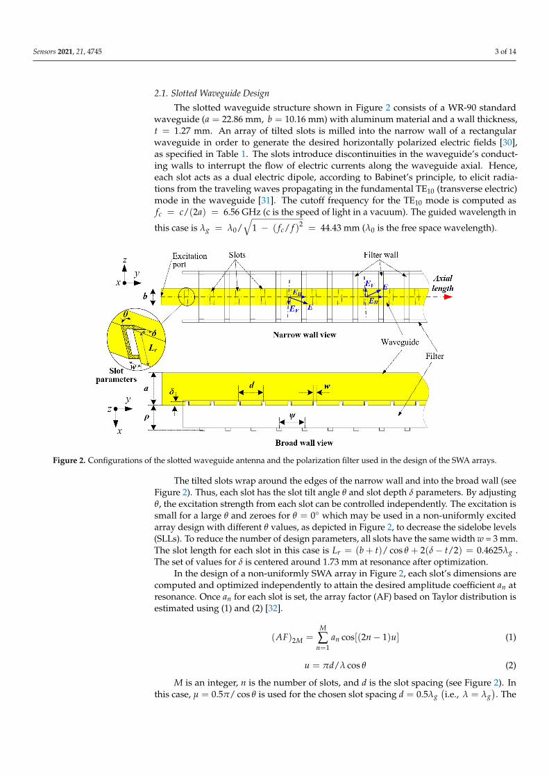
The instantaneous electric fields E from the inclined slots decompose into the hori-zontal EH and vertical EV fields, as depicted in Figure 2. As mentioned earlier, the verticalelectric fields EV among the adjacent slots cancel out as the adjacent slots have equal andopposite tilt angles. However, in practice, the slot tilt angle θ among the adjacent slotsvaries for optimization and amplitude distribution purposes. In addition, due to fabricationerrors, θ may differ from the numerical value in the simulation. Hence, the EV amongthe adjacent slots do not cancel out entirely due to the varying phases and magnitudes.Therefore, high sidelobes are observed in the horizontal (xy) plane due to the measurablelevels of unwanted cross-polarized signals (see Figure 3a).
Sensors 2021, 21, x FOR PEER REVIEW 4 of 15
slot to achieve the desired distribution to result in the radiation pattern computed as fol-lows:
( )sintotal gleE E AF= ⋅ (3)
Since the slotted waveguide structure in Figure 2 is fed at the excitation port and terminated in a matched load (absorber) to achieve a traveling wave antenna, its equiva-lent circuit becomes a parallel conductance G at resonance, whereas the reactive suscep-tance B cancels out. Hence, the resonant conductance 𝑔 of N slot is computed from the amplitude coefficient 𝑎 using (4), while the slot tilt angle 𝜃 is related to conductance 𝑔 by (5). Once the initial 𝜃 values are set, the slot tilt angle is further optimized to obtain the final range of values from −10° to 15°.
2
21
; 1,2,......,nn N
ii
ag n Na
=
= =
(4)
2900.7 237.6 2n n ng gθ = − + + (5)
The main beam, which is perpendicular to the waveguide axis, lies in the forward direction along the x-axis (see Figure 1) because of the slot spacing 𝑑 = 0.5𝜆 and oppo-site tilt angles among adjacent slots. Thus, the co-polarization due to the desired horizon-tally polarized electric fields 𝐸 (see Figure 2) is superimposed in the phase, whereas the vertically polarized electric fields 𝐸 , which contribute to undesired cross-polarization, among the adjacent slots, cancel out because they assume an equal amplitude but opposite direction. This phenomenon, in theory, inherently reduces the sidelobe levels of a wave-guide slot array due to the low levels of cross-polarized signals.
2.2. Polarization Filter The instantaneous electric fields E from the inclined slots decompose into the hori-
zontal 𝐸 and vertical 𝐸 fields, as depicted in Figure 2. As mentioned earlier, the verti-cal electric fields 𝐸 among the adjacent slots cancel out as the adjacent slots have equal and opposite tilt angles. However, in practice, the slot tilt angle 𝜃 among the adjacent slots varies for optimization and amplitude distribution purposes. In addition, due to fab-rication errors, 𝜃 may differ from the numerical value in the simulation. Hence, the 𝐸 among the adjacent slots do not cancel out entirely due to the varying phases and magnitudes. Therefore, high sidelobes are observed in the horizontal (𝑥𝑦) plane due to the measurable levels of unwanted cross-polarized signals (see Figure 3a).
(a) (b)
Figure 3. Radiation patterns of conventional SWA array. (a) Horizontal (𝑥𝑦) plane; (b) Vertical (𝑥𝑧) plane.
In order to significantly reduce the sidelobes, a polarization filter is positioned in front of the slotted waveguide, as shown in Figure 2. The filter constitutes equispaced
Figure 3. Radiation patterns of conventional SWA array. (a) Horizontal (xy) plane; (b) Vertical (xz) plane.
In order to significantly reduce the sidelobes, a polarization filter is positioned infront of the slotted waveguide, as shown in Figure 2. The filter constitutes equispacedorthogonal walls with a spacing parameter ψ ≤ 0.5λg to ensure adequate suppression

Sensors 2021, 21, 4745 5 of 14
of cross-polarized signals. The filter is positioned ρ distance away from the waveguidewall (see Figure 2). In principle, the effectiveness of the filter is inversely proportional towall spacing ψ and proportional to the distance ρ between the filter and the waveguidewall. However, the attenuation of the EV denoted by γ is determined primarily from thewall spacing ψ as expressed in (6) [33]. Referring to Figure 2, the filter’s orthogonal wallsare positioned in such a way that they stand in between the adjacent slots to limit theefficient propagation of undesired EV to guarantee the sidelobes’ suppression, as observedin Figure 3a.
γ =5.462 · ψ
·
√1 −
(2 · ψ
λ
)2
[dB/m] (6)
It should be noted that both the ψ and ρ parameters have an influence on the radi-ating slot and the radiation. Therefore, they are optimized and fixed as ψ = 6 mm andρ = 20 mm.
2.3. Reflector
Referring to Figure 1, the conventional slot array design has a reflector device witha flare-out angle to increase the antenna’s aperture to increase the gain from 24 dB to30 dB, as shown in Figure 3b, to satisfy the requirement in Table 1. Thus, the conven-tional SWA array has a dimension of 1920 mm × 165 mm × 84.3 mm (L × W × H).However, the SWA arrays with the reflector device are large in the antenna’s cross-section (i.e., yz-plane), mechanically complex, and weighty to rotate at a very high an-gular speed. The proposed antenna in Figure 1b is the result of the effort to designa reduced size SWA array by using a dielectric-inset structure, over which the boundsurface waves are excited. Thus, its vertical size is about half that of the conventionalcase (see Figure 1a), giving the same vertical (xz) plane beamwidth, and shows im-provement in weight and mechanical simplicity. After the full analysis of the SWAarrays in Figure 1 was performed, the following are the optimized design parameters:a = 22.86, b = 10.16 mm for WR − 90, L = 1920 mm, t = 1.27 mm, θ = −10◦ ∼ 15◦,δ = 1.73 mm, w = 3 mm, ψ = 6 mm, and ρ = 20 mm.
3. Design and Analysis of the Proposed Slotted Waveguide Array Antenna3.1. Evolution of the Proposed Case
To facilitate the development of the proposed antenna while still providing a physicalunderstanding of its geometrical structure, the three-dimensional SWA arrays in Figure 1 aremirrored in their two-dimensional analogues in the xz-plane, as shown in Figure 4. Thus, theevolution of the proposed case is demonstrated in Figure 4. The conventional antenna, TypeA, with a wide flare-angle reflector gives an ideal gain of more than 30 dB in Figure 5 at theexpense of large antenna size. The simplest approach to reduce the antenna’s physical size isby reducing the reflector size. Unfortunately, this approach results in a significant decreasein antenna gain.
The solution to this problem was accomplished by incorporating a tapered dielectric-inset guide structure in the SWA array to produce antenna Type B in Figure 4. This approachimmediately reduces the height of the conventional antenna by about 50%. However, inthe Type B antenna configuration, an optimum taper profile can only be achieved when thelength parameter Sx in the forward direction is very long, up to 2.5λ, which underminesthe antenna’s compactness. The relationship between Sx and the gain of the antenna canbe expressed mathematically in (7) [34].
Gain = 8Sx/λ (7)

Sensors 2021, 21, 4745 6 of 14
Sensors 2021, 21, x FOR PEER REVIEW 6 of 15
Thus, the incident, strongly bound surface wave field from the slotted waveguide, which is butted to the base of the dielectric structure, is transformed smoothly into a radi-ation field that is characterized by maximum antenna gain (see Figure 5, Type B) with an in-phase field.
Figure 4. Two-dimensional analogue of four different SWA array models in the xz (vertical) plane.
By truncating the long tapered section of the dielectric structure to produce antenna Type C (see Figure 4), the width of the antenna is reduced to 108 mm. Thus, a 29% size reduction is achieved in the forward direction as 𝑆 decreases to about 1.7𝜆. However, the gain of antenna Type C drops considerably to 26 dB in Figure 5a, since the phase dis-parity of the incident surface wave on the uniform cross-section of the truncated dielectric structure increases significantly. This causes the destructive interference of the surface wave field, transforming into a radiation field at the termination to result in a beam split (see Figure 5b, Type C).
Figure 4. Two-dimensional analogue of four different SWA array models in the xz (vertical) plane.
Sensors 2021, 21, x FOR PEER REVIEW 7 of 15
(a) (b)
Figure 5. Simulated results for different SWA array models. (a) Gain; (b) Patterns in vertical (xz) plane.
To solve the beam splitting problem of antenna Type C without resorting to an in-crease in the antenna’s size, the dielectric-inset guide structure was modified by tapering the termination with a staircase approximation to form the end-gradient in antenna Type D. The staircase model of the tapered dielectric is synthesized as a series of short slab segments, wherein the uniform cross-sectional areas in the forward direction are dimin-ished progressively, as shown in Figure 4. Thus, the width and height parameters of each dielectric slab segment of the staircase model of the taper profile were optimized individ-ually to allow for the redistribution of propagating signals in the dielectric medium so that at the dielectric–air interface, all the signals exiting the medium assume the same approximated phase velocity to maximize radiation efficiency. In effect, a conformal beam pattern is restored for the proposed SWA array Type D as the gain improves to about 29 dB in Figure 5. By incorporating the dielectric-inset guide structure into the SWA design, the proposed antenna, Type D, achieves a 62% size reduction while maintaining the an-tenna’s high gain result, which is comparable to the conventional case-Type A.
It should be noted that the long axial length (L) of the antenna is preserved in all the designs to ensure that the beam has a narrow width in the horizontal plane to satisfy the required half power beamwidth (HPBW) of 1.2°.
3.2. End Gradient Optimization The optimization of the dielectric-inset guide structure significantly improves the ra-
diation pattern of the antenna. The taper profile of the optimized dielectric structure is depicted in Figure 6, wherein the end gradient of the dielectric is synthesized as a series of dielectric slab segments of equal width ∆w and uniform cross-sectional areas of gradu-ally smaller heights 𝐻 , 𝑖 = 1, 2, … ,6. In other words, the tapered dielectric region is mod-eled as a sequence of sufficiently short (in terms of wavelength), uniform slab segments of diminishing cross-section in the forward direction, i.e., along the x-axis, as shown in Figure 6. The taper is segmented into five regions (𝑖 = 2,3, … , 6) with successively smaller heights. In this step-synthesis technique, the step discontinuity on the dielectric structure is regarded as a radiating aperture of a serial uniform slabs. At each step discon-tinuity, the fundamental transverse electric (TE) surface wave, which is assumed to be incident in the +𝑥 direction from 𝑥 = − ∞, is perturbed to cause redistribution of the instantaneous phases of the surface wave field on the uniform cross-section for phase matching. Consequently, the optimum taper profile of the dielectric is taken as one which smoothly transforms the strongly bound surface wave field into a radiation field with minimal phase disparity and reflection. This suggests that surface wave fields construc-tively interfere as they assume the same approximated phase velocity to maximize radia-tion efficiency.
Figure 5. Simulated results for different SWA array models. (a) Gain; (b) Patterns in vertical (xz) plane.
Thus, the incident, strongly bound surface wave field from the slotted waveguide,which is butted to the base of the dielectric structure, is transformed smoothly into aradiation field that is characterized by maximum antenna gain (see Figure 5, Type B) withan in-phase field.

Sensors 2021, 21, 4745 7 of 14
By truncating the long tapered section of the dielectric structure to produce antennaType C (see Figure 4), the width of the antenna is reduced to 108 mm. Thus, a 29% sizereduction is achieved in the forward direction as Sx decreases to about 1.7λ. However, thegain of antenna Type C drops considerably to 26 dB in Figure 5a, since the phase disparityof the incident surface wave on the uniform cross-section of the truncated dielectricstructure increases significantly. This causes the destructive interference of the surfacewave field, transforming into a radiation field at the termination to result in a beam split(see Figure 5b, Type C).
To solve the beam splitting problem of antenna Type C without resorting to anincrease in the antenna’s size, the dielectric-inset guide structure was modified by taperingthe termination with a staircase approximation to form the end-gradient in antennaType D. The staircase model of the tapered dielectric is synthesized as a series of shortslab segments, wherein the uniform cross-sectional areas in the forward direction arediminished progressively, as shown in Figure 4. Thus, the width and height parametersof each dielectric slab segment of the staircase model of the taper profile were optimizedindividually to allow for the redistribution of propagating signals in the dielectric mediumso that at the dielectric–air interface, all the signals exiting the medium assume the sameapproximated phase velocity to maximize radiation efficiency. In effect, a conformal beampattern is restored for the proposed SWA array Type D as the gain improves to about 29 dBin Figure 5. By incorporating the dielectric-inset guide structure into the SWA design, theproposed antenna, Type D, achieves a 62% size reduction while maintaining the antenna’shigh gain result, which is comparable to the conventional case-Type A.
It should be noted that the long axial length (L) of the antenna is preserved in all thedesigns to ensure that the beam has a narrow width in the horizontal plane to satisfy therequired half power beamwidth (HPBW) of 1.2◦.
3.2. End Gradient Optimization
The optimization of the dielectric-inset guide structure significantly improves the ra-diation pattern of the antenna. The taper profile of the optimized dielectric structure isdepicted in Figure 6, wherein the end gradient of the dielectric is synthesized as a seriesof dielectric slab segments of equal width ∆w and uniform cross-sectional areas of grad-ually smaller heights Hi, i = 1, 2, . . . , 6. In other words, the tapered dielectric region ismodeled as a sequence of sufficiently short (in terms of wavelength), uniform slab segmentsof diminishing cross-section in the forward direction, i.e., along the x-axis, as shown inFigure 6. The taper is segmented into five regions (i = 2, 3, . . . , 6) with successively smallerheights. In this step-synthesis technique, the step discontinuity on the dielectric structureis regarded as a radiating aperture of a serial uniform slabs. At each step discontinuity, thefundamental transverse electric (TE) surface wave, which is assumed to be incident in the+x direction from x = −∞, is perturbed to cause redistribution of the instantaneous phasesof the surface wave field on the uniform cross-section for phase matching. Consequently,the optimum taper profile of the dielectric is taken as one which smoothly transforms thestrongly bound surface wave field into a radiation field with minimal phase disparity andreflection. This suggests that surface wave fields constructively interfere as they assume thesame approximated phase velocity to maximize radiation efficiency.

Sensors 2021, 21, 4745 8 of 14Sensors 2021, 21, x FOR PEER REVIEW 8 of 15
Figure 6. Geometry of the staircase model of the tapered dielectric-inset guide structure depicting the end gradient and feed gradient.
The instantaneous phase of the radiation field from the dielectric surface with no ta-per profile received at points A, B, and C, assumed to be within the far-field region from the antenna, i.e., 𝑅 = 2𝐷 /𝜆 (maximum linear dimension of an antenna is D), is shown in Figure 7a. It can be noted that there is a significant phase difference between the received fields at these points, resulting in a scattering wave to cause reflection and destructive interference. However, the introduction of the taper region of the optimized dielectric structure modeled with staircase approximation, in Figure 6, leads to a substantial reduc-tion in the phase disparity at these received points within the desired band, as shown in Figure 7b. The radiation field at these points, therefore, assumes the same approximated phase velocity to mimic the behavior of a plane wave that maximizes radiation efficiency due to the constructive interference. The optimal taper profile of the dielectric in Figure 6 with the staircase model has geometrical parameters fixed as follows: ∆𝑤 = 4 mm, 𝐻 = 39.48 mm, 𝐻 = 36.33 mm, 𝐻 = 31.07 mm, 𝐻 = 26.64 mm and 𝐻 = 18.45 mm.
(a) (b)
Figure 7. Simulated phase responses at three different points from the antenna’s dielectric rod structure with (a) No taper profile; (b) Taper region modeled with the staircase approximation.
It should also be noted that the base of the dielectric-inset guide structure, where the slotted waveguide is butted, has also been tapered using the staircase approximation (see Figure 6) to result in a minimum reflection and gradually transition the incident, strongly bound field to the dielectric medium. This feed taper, therefore, significantly reduces the Voltage Standing Wave Ratio (VSWR) on the uniform section of the guide to improve the radiation characteristics of the antenna. The matching slab segments at the base of the
Figure 6. Geometry of the staircase model of the tapered dielectric-inset guide structure depictingthe end gradient and feed gradient.
The instantaneous phase of the radiation field from the dielectric surface with notaper profile received at points A, B, and C, assumed to be within the far-field regionfrom the antenna, i.e., R = 2D2/λ (maximum linear dimension of an antenna is D), isshown in Figure 7a. It can be noted that there is a significant phase difference betweenthe received fields at these points, resulting in a scattering wave to cause reflection anddestructive interference. However, the introduction of the taper region of the optimizeddielectric structure modeled with staircase approximation, in Figure 6, leads to a sub-stantial reduction in the phase disparity at these received points within the desired band,as shown in Figure 7b. The radiation field at these points, therefore, assumes the sameapproximated phase velocity to mimic the behavior of a plane wave that maximizesradiation efficiency due to the constructive interference. The optimal taper profile of thedielectric in Figure 6 with the staircase model has geometrical parameters fixed as follows:∆ w = 4 mm, H2 = 39.48 mm, H3 = 36.33 mm, H4 = 31.07 mm, H5 = 26.64 mm andH6 = 18.45 mm.
Sensors 2021, 21, x FOR PEER REVIEW 8 of 15
Figure 6. Geometry of the staircase model of the tapered dielectric-inset guide structure depicting the end gradient and feed gradient.
The instantaneous phase of the radiation field from the dielectric surface with no ta-per profile received at points A, B, and C, assumed to be within the far-field region from the antenna, i.e., 𝑅 = 2𝐷 /𝜆 (maximum linear dimension of an antenna is D), is shown in Figure 7a. It can be noted that there is a significant phase difference between the received fields at these points, resulting in a scattering wave to cause reflection and destructive interference. However, the introduction of the taper region of the optimized dielectric structure modeled with staircase approximation, in Figure 6, leads to a substantial reduc-tion in the phase disparity at these received points within the desired band, as shown in Figure 7b. The radiation field at these points, therefore, assumes the same approximated phase velocity to mimic the behavior of a plane wave that maximizes radiation efficiency due to the constructive interference. The optimal taper profile of the dielectric in Figure 6 with the staircase model has geometrical parameters fixed as follows: ∆𝑤 = 4 mm, 𝐻 = 39.48 mm, 𝐻 = 36.33 mm, 𝐻 = 31.07 mm, 𝐻 = 26.64 mm and 𝐻 = 18.45 mm.
(a) (b)
Figure 7. Simulated phase responses at three different points from the antenna’s dielectric rod structure with (a) No taper profile; (b) Taper region modeled with the staircase approximation.
It should also be noted that the base of the dielectric-inset guide structure, where the slotted waveguide is butted, has also been tapered using the staircase approximation (see Figure 6) to result in a minimum reflection and gradually transition the incident, strongly bound field to the dielectric medium. This feed taper, therefore, significantly reduces the Voltage Standing Wave Ratio (VSWR) on the uniform section of the guide to improve the radiation characteristics of the antenna. The matching slab segments at the base of the
Figure 7. Simulated phase responses at three different points from the antenna’s dielectric rod structure with (a) No taperprofile; (b) Taper region modeled with the staircase approximation.
It should also be noted that the base of the dielectric-inset guide structure, wherethe slotted waveguide is butted, has also been tapered using the staircase approxima-tion (see Figure 6) to result in a minimum reflection and gradually transition the inci-dent, strongly bound field to the dielectric medium. This feed taper, therefore, signifi-
Sensors 2021, 21, 4745 9 of 14
cantly reduces the Voltage Standing Wave Ratio (VSWR) on the uniform section of theguide to improve the radiation characteristics of the antenna. The matching slab seg-ments at the base of the dielectric structure in Figure 6 have been optimized and fixed as:∆wa = 2 mm, ∆wb = 3 mm, ∆wc = 5 mm, Ha = 10 mm, Hb = 20 mm, and Hc = 35 mm.
3.3. Dielectric Material Selection
The selection of a proper dielectric material for the design of the antenna’s dielectricstructure is primarily based on the material’s relative permittivity (εr), loss tangent (tan δ),and most importantly, weight or density. It is evident that as εr increases, the bandwidthreduces, and the radiation efficiency decreases due to the increase in the quality factor(Q-factor). It should be noted that as the εr increases, the dielectric component no longerworks under the TE10 mode required for a low sidelobe and high gain. This suggests thatthe lower the εr, the higher the radiation power for a fixed tan δ, as shown in Figure 8.Furthermore, extremely lightweight materials are highly recommended for the design ofa dielectric component, since heavy materials undermine the compactness achieved bythe proposed SWA array. Thus, to choose the right material for the dielectric component,several property data among commercial dielectric materials are compared in Table 2. Itshould be noted that model D has the lightest weight in terms of density and the lowest εramong the materials. Therefore, it is chosen as the material of the dielectric component ofthe proposed antenna.
Sensors 2021, 21, x FOR PEER REVIEW 9 of 15
dielectric structure in Figure 6 have been optimized and fixed as: ∆𝑤 = 2 mm, ∆𝑤 = 3 mm, ∆𝑤 = 5 mm, 𝐻 = 10 mm, 𝐻 = 20 mm, and 𝐻 = 35 mm. 3.3. Dielectric Material Selection
The selection of a proper dielectric material for the design of the antenna’s dielectric structure is primarily based on the material’s relative permittivity (𝜀 ) , loss tan-gent (tan𝛿), and most importantly, weight or density. It is evident that as 𝜀 increases, the bandwidth reduces, and the radiation efficiency decreases due to the increase in the qual-ity factor (Q-factor). It should be noted that as the 𝜀 increases, the dielectric component no longer works under the TE10 mode required for a low sidelobe and high gain. This suggests that the lower the 𝜀 , the higher the radiation power for a fixed tan𝛿, as shown in Figure 8. Furthermore, extremely lightweight materials are highly recommended for the design of a dielectric component, since heavy materials undermine the compactness achieved by the proposed SWA array. Thus, to choose the right material for the dielectric component, several property data among commercial dielectric materials are compared in Table 2. It should be noted that model D has the lightest weight in terms of density and the lowest ɛ among the materials. Therefore, it is chosen as the material of the dielectric component of the proposed antenna.
Table 2. Comparison of the properties of different dielectric materials.
Material A B C D Relative permittivity (𝜀 ) 2.1 2.53 1.7 1.53
Loss tangent (tan𝛿) 0.00015 0.0001 0.0001 0.00035 Density (kg/cm ) 2.2 1 × 10 1 × 10 8 × 10
Figure 8. Normalized radiation power from the dielectric rod structure with varied relative permit-tivity, ɛ .
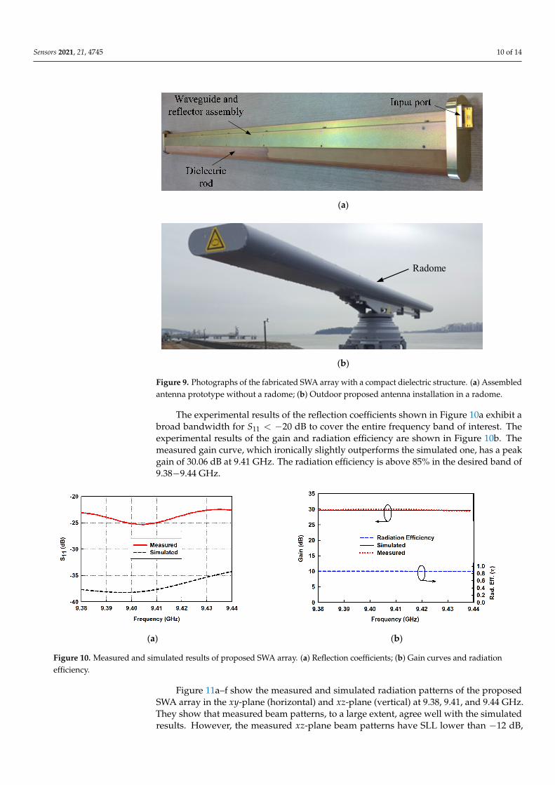
4. Results and Discussions Figure 9a,b show a photograph of the fabricated SWA array and outdoor antenna
installation with a radome, respectively.
Figure 8. Normalized radiation power from the dielectric rod structure with varied relative permit-tivity, εr.
Table 2. Comparison of the properties of different dielectric materials.
Material A B C D
Relative permittivity (εr) 2.1 2.53 1.7 1.53Loss tangent (tan δ) 0.00015 0.0001 0.0001 0.00035Density (kg/cm3) 2.2 1 × 10⁻³ 1 × 10⁻³ 8 × 10⁻⁵
4. Results and Discussion
Figure 9a,b show a photograph of the fabricated SWA array and outdoor antennainstallation with a radome, respectively.
Sensors 2021, 21, 4745 10 of 14Sensors 2021, 21, x FOR PEER REVIEW 10 of 15
(a)
Radome
(b)
Figure 9. Photographs of the fabricated SWA array with a compact dielectric structure. (a) Assem-bled antenna prototype without a radome; (b) Outdoor proposed antenna installation in a radome.
The experimental results of the reflection coefficients shown in Figure 10a exhibit a broad bandwidth for 𝑆 < −20 dB to cover the entire frequency band of interest. The experimental results of the gain and radiation efficiency are shown in Figure 10b. The measured gain curve, which ironically slightly outperforms the simulated one, has a peak gain of 30.06 dB at 9.41 GHz. The radiation efficiency is above 85% in the desired band of 9.38−9.44 GHz.
(a) (b)
Figure 10. Measured and simulated results of proposed SWA array. (a) Reflection coefficients; (b) Gain curves and radia-tion efficiency.
Figure 11a–f show the measured and simulated radiation patterns of the proposed SWA array in the 𝑥𝑦-plane (horizontal) and 𝑥𝑧-plane (vertical) at 9.38, 9.41, and 9.44 GHz.
Figure 9. Photographs of the fabricated SWA array with a compact dielectric structure. (a) Assembledantenna prototype without a radome; (b) Outdoor proposed antenna installation in a radome.
The experimental results of the reflection coefficients shown in Figure 10a exhibit abroad bandwidth for S11 < −20 dB to cover the entire frequency band of interest. Theexperimental results of the gain and radiation efficiency are shown in Figure 10b. Themeasured gain curve, which ironically slightly outperforms the simulated one, has a peakgain of 30.06 dB at 9.41 GHz. The radiation efficiency is above 85% in the desired band of9.38−9.44 GHz.
Sensors 2021, 21, x FOR PEER REVIEW 10 of 15
(a)
Radome
(b)
Figure 9. Photographs of the fabricated SWA array with a compact dielectric structure. (a) Assem-bled antenna prototype without a radome; (b) Outdoor proposed antenna installation in a radome.
The experimental results of the reflection coefficients shown in Figure 10a exhibit a broad bandwidth for 𝑆 < −20 dB to cover the entire frequency band of interest. The experimental results of the gain and radiation efficiency are shown in Figure 10b. The measured gain curve, which ironically slightly outperforms the simulated one, has a peak gain of 30.06 dB at 9.41 GHz. The radiation efficiency is above 85% in the desired band of 9.38−9.44 GHz.
(a) (b)
Figure 10. Measured and simulated results of proposed SWA array. (a) Reflection coefficients; (b) Gain curves and radia-tion efficiency.
Figure 11a–f show the measured and simulated radiation patterns of the proposed SWA array in the 𝑥𝑦-plane (horizontal) and 𝑥𝑧-plane (vertical) at 9.38, 9.41, and 9.44 GHz.
Figure 10. Measured and simulated results of proposed SWA array. (a) Reflection coefficients; (b) Gain curves and radiationefficiency.
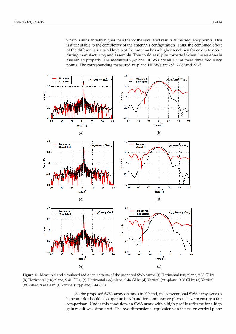
Figure 11a–f show the measured and simulated radiation patterns of the proposedSWA array in the xy-plane (horizontal) and xz-plane (vertical) at 9.38, 9.41, and 9.44 GHz.They show that measured beam patterns, to a large extent, agree well with the simulatedresults. However, the measured xz-plane beam patterns have SLL lower than −12 dB,
Sensors 2021, 21, 4745 11 of 14
which is substantially higher than that of the simulated results at the frequency points. Thisis attributable to the complexity of the antenna’s configuration. Thus, the combined effectof the different structural layers of the antenna has a higher tendency for errors to occurduring manufacturing and assembly. This could easily be corrected when the antenna isassembled properly. The measured xy-plane HPBWs are all 1.2◦ at these three frequencypoints. The corresponding measured xz-plane HPBWs are 28◦, 27.8◦and 27.7◦.
Sensors 2021, 21, x FOR PEER REVIEW 11 of 15
They show that measured beam patterns, to a large extent, agree well with the simulated results. However, the measured 𝑥𝑧-plane beam patterns have SLL lower than −12 dB, which is substantially higher than that of the simulated results at the frequency points. This is attributable to the complexity of the antenna’s configuration. Thus, the combined effect of the different structural layers of the antenna has a higher tendency for errors to occur during manufacturing and assembly. This could easily be corrected when the an-tenna is assembled properly. The measured 𝑥𝑦-plane HPBWs are all 1.2° at these three frequency points. The corresponding measured 𝑥𝑧-plane HPBWs are 28°, 27.8°and 27.7°
(a) (b)
(c) (d)
(e) (f)
Figure 11. Measured and simulated radiation patterns of the proposed SWA array. (a) Horizontal (𝑥𝑦)-plane, 9.38 GHz; (b) Horizontal (𝑥𝑦)-plane, 9.41 GHz; (c) Horizontal (𝑥𝑦)-plane, 9.44 GHz; (d) Vertical (𝑥𝑧)-plane, 9.38 GHz; (e) Vertical (𝑥𝑧)-plane, 9.41 GHz; (f) Vertical (𝑥𝑧)-plane, 9.44 GHz.
Figure 11. Measured and simulated radiation patterns of the proposed SWA array. (a) Horizontal (xy)-plane, 9.38 GHz;(b) Horizontal (xy)-plane, 9.41 GHz; (c) Horizontal (xy)-plane, 9.44 GHz; (d) Vertical (xz)-plane, 9.38 GHz; (e) Vertical(xz)-plane, 9.41 GHz; (f) Vertical (xz)-plane, 9.44 GHz.
As the proposed SWA array operates in X-band, the conventional SWA array, set as abenchmark, should also operate in X-band for comparative physical size to ensure a faircomparison. Under this condition, an SWA array with a high-profile reflector for a highgain result was simulated. The two-dimensional equivalents in the xz or vertical plane

Sensors 2021, 21, 4745 12 of 14
of the proposed and conventional models are shown in Figure 12a. The simulated gaincurves are plotted in Figure 12b.
• Ant-A: Proposed SWA array comprising of a slotted waveguide, compact dielectricstructure, and miniaturized reflector.
• Ant-B: Commercial SWA array composed of a slotted waveguide and a relativelylarger reflector.
Sensors 2021, 21, x FOR PEER REVIEW 13 of 15
(a) (b)
Figure 12. (a) Two dimensional analogues in 𝑥𝑧 (vertical) plane; (b) Gain results of the simulated conventional and pro-posed SWA arrays.
5. Conclusions In summary, a new configuration of slotted waveguide array (SWA) antennas, com-
prising a slotted waveguide, polarizing filter, and tapered dielectric-inset guide structure, was proposed for use in a shipboard marine radar in X-band. The concept of using the dielectric-inset guide structure to reduce the size of an SWA array was presented. Com-parison between the proposed and the conventional SWA arrays was also presented, con-firming the practicality of this approach. The experimental results indicated that a size reduction of 62% could easily be achieved for the SWA array, while preserving the an-tenna’s superior performance, i.e., a higher gain and radiation efficiency at the same time. A staircase model of the tapered section of the implemented dielectric structure was in-troduced. The incident, guided surface wave field on the uniform cross-section was per-turbed for phase matching purposes to ensure that it transformed into a radiation field that is characterized by the maximum intensity with little reflection. Thus, the antenna exhibited a peak gain of 30.06 dB and radiation efficiency above 80% in the desired band of 9.38~9.44 GHz. The measured horizontal plane HPBWs are about 1.2° at the various frequency points. The corresponding measured 𝑥𝑧-plane HPBWs are about 28°. The se-lected dielectric has low-density properties to maintain low weight. This proposed SWA array has promising physical and electrical features, making it more suitable for modern marine radar applications than the conventional case.
Author Contributions: K.A. designed, simulated, and optimized the proposed slotted waveguide antenna array. H.A.D contributed to the preparation of this article. K.A. prepared this article, in-cluding its revision. Y.-B.J. provide the suggestions regarding the design, measurement, and prep-aration of this article and is the supervisor of the research group. All authors have read and agreed to the published version of the manuscript.
Funding: This research received no external funding.
Institutional Review Board Statement: Not applicable.
Informed Consent Statement: Not applicable.
Data Availability Statement: Not applicable.
Figure 12. (a) Two dimensional analogues in xz (vertical) plane; (b) Gain results of the simulated conventional and proposedSWA arrays.
The proposed antenna possesses an average gain of 29 dB, which has been found to becomparable to that of the conventional type. However, the proposed antenna configurationachieves a 50% size reduction in lateral size that lies along the z-axis and 29% in the forwardor radiation direction along the x-axis. Thus, the antenna’s total size is reduced by 62%,while keeping its high gain within the band of interest. Moreover, a low loss, low-densitymaterial was chosen for the design of the dielectric structure to maintain this physicaladvantage over the conventional counterpart without resulting in a heavy weight andlow efficiency.
Table 3 compares the requirements of the marine radar to the measurement dataof the proposed SWA array. It shows that the proposed SWA array can fulfil all of therequirements except for the SLL in the vertical plane. This is primarily due to fabricationand assembly errors, which may result from misalignment between the different structuralcomponents of the proposed SWA array. Thus, proper assembly of the various componentswill easily alleviate the high SLL in the measured results.

Sensors 2021, 21, 4745 13 of 14
Table 3. Comparison between the requirements and the measured data.
Parameters Requirement Numerical Data Measured Data
Frequency 9.4 GHz 9.4 GHz 9.4 GHz o
Gain ≥ 28 dB ≥ 29.62 dB ≥ 29.4 dB o
VSWR ≤ 1.5 ≤ 1.5 ≤ 1.5 o
Polarization Horizontal Horizontal Horizontal o
BeamwidthHorizontal (Az) ≤ 1.2◦ ≤ 1.2◦ ≤ 1.2◦ o
Vertical (El) ≥ 20◦ ≥ 27.7◦ ≥ 27.8◦ o
SLLHorizontal (Az) ≤ −20 dB ≤ −20 dB ≤ −20.8 dB o
Vertical (El) ≤ −30 dB ≤ −31 dB ≤ −12 dB XAz and El denote azimuth and elevation planes, respectively.
5. Conclusions
In summary, a new configuration of slotted waveguide array (SWA) antennas, com-prising a slotted waveguide, polarizing filter, and tapered dielectric-inset guide structure,was proposed for use in a shipboard marine radar in X-band. The concept of using thedielectric-inset guide structure to reduce the size of an SWA array was presented. Com-parison between the proposed and the conventional SWA arrays was also presented,confirming the practicality of this approach. The experimental results indicated that asize reduction of 62% could easily be achieved for the SWA array, while preserving theantenna’s superior performance, i.e., a higher gain and radiation efficiency at the sametime. A staircase model of the tapered section of the implemented dielectric structure wasintroduced. The incident, guided surface wave field on the uniform cross-section wasperturbed for phase matching purposes to ensure that it transformed into a radiation fieldthat is characterized by the maximum intensity with little reflection. Thus, the antennaexhibited a peak gain of 30.06 dB and radiation efficiency above 80% in the desired band of9.38~9.44 GHz. The measured horizontal plane HPBWs are about 1.2◦ at the various fre-quency points. The corresponding measured xz-plane HPBWs are about 28◦. The selecteddielectric has low-density properties to maintain low weight. This proposed SWA arrayhas promising physical and electrical features, making it more suitable for modern marineradar applications than the conventional case.
Author Contributions: K.A. designed, simulated, and optimized the proposed slotted waveguideantenna array. H.A.D. contributed to the preparation of this article. K.A. prepared this article,including its revision. Y.-B.J. provide the suggestions regarding the design, measurement, andpreparation of this article and is the supervisor of the research group. All authors have read andagreed to the published version of the manuscript.
Funding: This research received no external funding.
Institutional Review Board Statement: Not applicable.
Informed Consent Statement: Not applicable.
Data Availability Statement: Not applicable.
Conflicts of Interest: The authors declare no conflict of interest.
References1. Da Costa, I.F.; Spadoti, D.H.; Cerqueira, S.A. Dual-band slotted waveguide antenna array for communication, maritime navigation
and surveillance radar. In Proceedings of the 2015 International Workshop on Telecommunications (IWT), Santa Rita do Sapucai,Brazil, 14–17 June 2015.
2. Maa, J.P.-Y.; Ha, H.K. X-Band Radar Wave Observation System. Available online: http://139.70.23.12/people/maa_jp/pubs/X-band%20radar%20wave%20Observation%20system.pdf (accessed on 11 July 2021).
3. Wang, H.; Hu, H.; Chung, S. High gain slot-pair substrate-integrated-waveguide antenna for 77 GHz vehicle collision warningradar. In Proceedings of the 2014 11th European Radar Conference, Rome, Italy, 6–9 October 2014.

Sensors 2021, 21, 4745 14 of 14
4. Dolan, B.A.; Ruthledge, S.A. An Integrated Display and Analysis Methodology for Multivariable Radar Data. J. Appl. Meteorol.Climatol. 2007, 46, 1196–1213. [CrossRef]
5. Mirzaei, G.; Jamali, M.M.; Ross, J.; Gorsevski, P.V.; Bingman, V.P. Data fusion of acoustics, infrared, and marine radar for avianstudy. IEEE Sens. J. 2015, 15, 6625–6632. [CrossRef]
6. Young, R.; Rosenthal, W.; Ziemer, F. A three-dimensional analysis of marine radar images for the determination of ocean wavedirectionality and surface currents. J. Geophys. Res. 1985, 90, 1049–1059. [CrossRef]
7. Jung, Y.-B.; Yeom, I.; Jung, C.W. Centre-fed series array antenna for k-/ka-band electromagnetic sensors. IET Microw. AntennasPropag. 2012, 6, 588–593. [CrossRef]
8. Hajian, M.; Zijderveld, J.; Lestari, A.A.; Ligthart, L.P. Analysis, design and measurement of a series-fed microstrip array antennafor X-band INDRA: The Indonesian maritime radar. In Proceedings of the 3rd European Conference on Antennas and Propagation,Berlin, Germany, 23–27 March 2009; pp. 1154–1157.
9. Huque, T.; Hossain, K.; Islam, S.; Chowdhury, A. Design and performance analysis of microstrip array antennas with optimumparameters for X-band applications. Int. J. Adv. Comput. Sci. Applicat. 2011, 2, 81–87.
10. Hautcoeur, J.; Cruz, E.M.; Bartholomew, J.; Sarrazin, J.; Mahe, Y.; Toutain, S. Low-cost printed antenna array built with hybridfeed for urban microwave links. IET Microw. Antennas Propag. 2010, 4, 1320–1326. [CrossRef]
11. Iizuka, H.; Sakakibara, K.; Watanabe, T.; Sato, K.; Nishikawa, K. Millimeter-wave microstrip array antenna with high efficiencyfor automotive radar systems. R&D Rev. Toyota CRDL 2002, 37, 7–12.
12. Barba, M. A high-isolation, wideband and dual-linear polarization patch antenna. IEEE Trans. Antennas Propag. 2008, 56,1472–1476. [CrossRef]
13. Lee, B.; Kwon, S.; Choi, J. Polarisation diversity microstrip base station antenna at 2 GHz using t-shaped aperture-coupled feeds.IEE Proc. Microw. Antennas Propag. 2001, 148, 334–338. [CrossRef]
14. Li, B.; Yin, Y.-Z.; Hu, W.; Ding, Y.; Zhao, Y. Wideband dual-polarized patch antenna with low cross polarization and high isolation.IEEE Antennas Wirel. Propag. Lett. 2012, 11, 427–430.
15. Bayderkhani, R.; Hassani, H.R. Wideband and low sidelobe slot antenna fed by series-fed printed array. IEEE Trans. AntennasPropag. 2010, 58, 3898–3904. [CrossRef]
16. Levine, E.; Malamud, G.; Shtrikman, S.; Treves, D. A study of microstrip array antennas with the feed network. IEEE Trans.Antennas Propag. 1989, 37, 426–434. [CrossRef]
17. Huang, J. A Ka-band circularly polarized high-gain microstrip array. In Proceedings of the IEEE Antennas and PropagationSociety International Symposium and URSI National Radio Science Meeting, Seattle, WA, USA, 20–24 June 1994.
18. James, J.R.; Hall, P.S.; Wood, C. Microstrip Antenna Theory and Design; Peter Peregrinus: London, UK, 1981.19. Mailloux, R.; McIlvenna, J.; Kernweis, N. Microstrip array technology. IEEE Trans. Antennas Propag. 1981, 29, 25–37. [CrossRef]20. Weiss, M. Microstrip antennas for millimeter waves. IEEE Trans. Antennas Propag. 1981, 29, 171–174. [CrossRef]21. Rengarajan, S.R. Advances in Slotted Waveguide Array Antenna Technology. In Proceedings of the 2019 IEEE International
Conference on Microwaves, Antennas, Communications and Electronic Systems (COMCAS), Tel-Aviv, Israel, 4–6 November 2019.22. Coetzee, J.C.; Sheel, S. Waveguide Slot Array Design WITH Compensation for Higher Order Mode Coupling Between Inclined
Coupling Slots and Neighboring Radiating Slots. IEEE Trans. Antennas Propag. 2019, 67, 378–389. [CrossRef]23. Misilmani, H.M.E.; Al-Husseini, M.; Kabalan, K.Y.; El-Hajj, A. A design procedure for slotted waveguide antennas with specified
sidelobe levels. In Proceedings of the 2014 International Conference on High Performance Computing & Simulation (HPCS),Bologna, Italy, 21–25 July 2014; pp. 828–832.
24. Pradeep, K.S.; Nagendra, N.N.; Manjunath, R.K. Design and Simulation of Slotted Waveguide Antenna Array for X-Band Radars.In Proceedings of the 2018 4th International Conference for Convergence in Technology (I2CT), Mangalore, India, 27–28 October2018; pp. 1–6.
25. Hung, K.-L.; Chou, H.-T. A design of slotted waveguide antenna array operated at X-band. In Proceedings of the 2010 IEEEInternational Conference on Wireless Information Technology and Systems, Honolulu, HI, USA, 28 August–3 September 2010;pp. 1–4.
26. Elliott, R.S. An improved design procedure for small arrays of shunt slots. IEEE Trans. Antennas Propag. 1983, 31, 48–53. [CrossRef]27. Elliott, R.; O’Loughlin, W. The design of slot arrays including internal mutual coupling. IEEE Trans. Antennas Propag. 1986, 34,
1149–1154. [CrossRef]28. Elliott, R.S. The design of waveguide-fed slot arrays. In Antenna Handbook; Van Nostrand: New York, NY, USA, 1988.29. Yusuf, D.P.; Zulkifli, F.Y.; Rahardjo, E.T. Design of Narrow-wall Slotted Waveguide Antenna with V-shaped Metal Reflector for
X-Band Radar Application. In Proceedings of the 2018 International Symposium on Antennas and Propagation (ISAP), Busan,Korea, 23–26 October 2018.
30. Enjiu, R.K.; Bender, M. Slotted Waveguide Antenna Design Using 3D EM Simulation. Microw. J. 2013, 56, 72.31. Volakis, J. Antenna Engineering Handbook; McGraw-Hill Professional: New York, NY, USA, 2007.32. Balanis, C.A. Antenna Theory and Design; John Wiley & Sons, Inc.: Hoboken, NJ, USA, 1997; pp. 385–424.33. Mazur, M.; Wisniewski, J. Performance of cross-polarization filter dedicated for slotted waveguide antenna array. In Proceedings
of the 2010 IEEE Radar Conference, Arlington, VA, USA, 10–14 May 2010; pp. 1335–1338.34. Meng, R.; Zhu, Q. Design of a compact high gain end-fire dielectric rod antenna. In Proceedings of the 2016 IEEE International
Symposium on Antennas and Propagation (APSURSI), Fajardo, PR, USA, 26 June–1 July 2016.