
(PDF) Experimental Research of High-Temperature and High ...
Upload
khangminh22Category
view
0download
0
UNIVERSITY OF CALIFORNIA, SAN DIEGO
High Power High Linearity Waveguide Photodiodes:
Measurement, Modeling, and Characterization
for Analog Optical Links
A dissertation submitted in partial satisfaction of the
requirements for the degree Doctor of Philosophy
in
Electrical Engineering (Photonics)
by
Meredith Nicole Draa
Committee in Charge:
Professor Paul K. L. Yu, Chair Professor William S. Chang Professor Richard K. Herz Professor William Hodgkiss Professor Yu-Hwa Lo
2010

Copyright
Meredith Nicole Draa, 2010
All rights reserved.

iii
The Dissertation of Meredith Nicole Draa is approved, and it is acceptable in
quality and form for publication on microfilm and electronically:
Chair
University of California, San Diego
2010

iv
Dedication
This dissertation is dedicated to my husband, David, for all his love,
understanding, and support throughout all these years. He has remained ever willing to
sacrifice and adapt to career moves that I have been lucky enough to be offered in pursuit
of my Ph. D. For this, I am eternally grateful.

v
Table of Contents
Signature Page..................................................................................................................... iii Dedication........................................................................................................................... iv Table of Contents................................................................................................................. v List of Figures................................................................................................................... viii List of Tables..................................................................................................................... xii Acknowledgements........................................................................................................... xiii Vita.................................................................................................................................... xvi Abstract of the Dissertation............................................................................................... xviii
Chapter 1 Introduction....................................................................................................... 1
1.1 "About light, I am in the dark".................................................................................. 1
1.2 Why Analog Optical Systems?.................................................................................. 2
1.2.1 Overview...................................................................................................... 2
1.2.2 Electronic Versus Photonic............................................................................ 2
1.2.3 Figures of Merit............................................................................................. 3
1.3 Photodiode Background and Needs........................................................................... 5
1.3.1 PIN Photodiodes............................................................................................ 5
1.3.2 State of PIN Photodiodes............................................................................... 8
1.3.3 Uni-traveling Carrier Photodiodes.................................................................. 9
1.3.4 Design and Considerations................................................................................... 14
1.4 Motivation............................................................................................................. 20
1.5 Scope of Dissertation............................................................................................. 21
1.6 References............................................................................................................. 24
Chapter 2 Nonlinearity and Measurement Systems........................................................... 30
2.1 Introduction........................................................................................................... 30
2.2 Background and Motivation.................................................................................... 31
2.2.1 Introduction to IP3........................................................................................ 31
2.2.2 Importance of IP3 to Modulation Systems..................................................... 32
2.3 Measurement Schemes........................................................................................... 33
2.3.1 Two-Tone Heterodyne Setup........................................................................ 33
2.3.2 Two-Tone Mach-Zehnder Modulator (MZM) Setup....................................... 34

vi
2.3.3 Three-Laser Two-Tone MZM Setup............................................................. 36
2.3.4 Four-Laser Three-Tone MZM Setup............................................................ 37
2.4 Three-Laser Two-Tone Setup................................................................................. 38
2.4.1 Introduction................................................................................................. 38
2.4.2 Experiment I: Second and Third Order Intercept Measurement....................... 38
2.4.3 Experiment II: Investigating the MZM Nonlinearity....................................... 41
2.4.4 Analytical Characterization.......................................................................... 44
2.4.5 Summary.................................................................................................... 51
2.5 Comparing Nonlinearity Measurement Systems....................................................... 52
2.5.1 Background and Motivation......................................................................... 52
2.5.2 Measurement Setups.................................................................................... 54
2.5.3 Mathematical Relationships.......................................................................... 54
2.5.4 Results and Analysis.................................................................................... 59
2.5.5 Polarization Investigation..................................................................................... 67
2.5.6 Summary.................................................................................................... 71
2.6 Conclusion............................................................................................................ 71
2.7 Acknowledgements................................................................................................ 72
2.8 References............................................................................................................. 74
Chapter 3 Nonlinearity in PIN Waveguide Photodiodes.................................................... 76
3.1 Introduction........................................................................................................... 76
3.2 Background........................................................................................................... 77
3.2.1 Surface Normal PIN Photodiodes.................................................................. 77
3.2.2 Waveguide PIN Photodiodes........................................................................ 80
3.2.3 PIN versus UTC Waveguide Photodiodes............................................................ 82
3.3 Device Structures and Modeling............................................................................. 82
3.3.1 Device Structures......................................................................................... 82
3.3.2 Electrical Simulation.................................................................................... 85
3.3.3 Thermal Simulation..................................................................................... 88
3.4 Experimental Results and Discussion...................................................................... 90
3.4.1 Bandwidth Measurement.............................................................................. 90
3.4.2 DC Saturation.............................................................................................. 92
3.4.3 Nonlinearity Measurement........................................................................... 93

vii
3.5 Nonlinearity Modeling by Equivalent Circuit Analysis............................................. 98
3.6 Conclusion.......................................................................................................... 102
3.7 Acknowledgements.............................................................................................. 103
3.8 References........................................................................................................... 105
Chapter 4 Uni-Traveling Carrier Directional Coupler Photodiode.................................. 107
4.1 Introduction......................................................................................................... 107
4.2 Device Design..................................................................................................... 109
4.3 Baseline Device................................................................................................... 113
4.3.1 Electrical and Thermal Simulation.............................................................. 113
4.3.2 Responsivity Measurement......................................................................... 119
4.3.3 Bandwidth Measurement............................................................................ 121
4.3.4 Nonlinearity Measurement.......................................................................... 122
4.4 Device Variations................................................................................................. 129
4.4.1 Variation Designs...................................................................................... 129
4.4.2 Thermal Simulation………………………....………………………………… 129
4.4.3 Responsivity Measurement......................................................................... 132
4.4.4 Bandwidth Measurement............................................................................ 135
4.4.5 Voltage-Dependent Nonlinearities............................................................... 136
4.5 Conclusion.......................................................................................................... 142
4.6 Acknowledgements.............................................................................................. 145
4.7 References........................................................................................................... 146
Chapter 5 Conclusion and Future Work......................................................................... 149
5.1 Summary............................................................................................................. 149
5.2 Future Work........................................................................................................ 153
5.2.1 Nonlinearity Investigations......................................................................... 153
5.2.2 Nonlinearity Modeling............................................................................... 154
5.2.3 Redesigning the UTC DCPD...................................................................... 156
5.3 Conclusion.......................................................................................................... 158
5.4 Acknowledgements.............................................................................................. 159
5.5 References........................................................................................................... 160
Appendix A...................................................................................................................... 161
Appendix B...................................................................................................................... 164

viii
List of Figures
Figure 1.1. (a) Electronic transmitter and (b) equivalent photonic transmitter...................... 3 Figure 1.2. Reverse biased PIN photodiode...................................................................... 6 Figure 1.3. IV curve for photodiode with increasing photocurrent...................................... 6 Figure 1.4. Spectral responsivity for AlGaN-p/GaN p-i-n photodetector (solid), compared to
that for homogeneous GaN p-i-n photodetector (dotted) [28]............................ 9 Figure 1.5. Bandgap structure of a UTC photodiode........................................................ 10 Figure 1.6. InGaAs-InP MUTC photodiode structure [40]................................................ 11 Figure 1.7. Micrograph of the fabricated UTC-PD with an integrated matching circuit
[41]............................................................................................................. 12 Figure 1.8. OIP3 as a function of the dc photocurrent for PD A and PD B at -5V bias
[42]............................................................................................................. 13 Figure 1.9. Schematic cross-sectional view of RFPD [43]................................................ 14 Figure 1.10. Dependence of three tone IP3 for pin-RFPD and UTC-RFPD on average
photocurrent at 3V bias [44]......................................................................... 14 Figure 1.11. Schematic of velocity matched PD showing passive optical waveguide, active
PIN PDs and microwave transmission line [58]............................................. 16 Figure 1.12. (a) Three-tone IMD3 measurement at 60mA (b) Comparison of Two-Tone and
Three-Tone OIP3 (with 3dB correction factor) [66]........................................ 17 Figure 1.13. Calculated space-charge electric field in the intrinsic region at currents of 0.1
(solid) and 1 (dashed) mA, with simulated spot size of 7µm [67]..................... 19 Figure 1.14. Measured second harmonic power of the 0.95µm PD showing the regimes of
importance for the dominating nonlinear mechanisms [67]............................. 19 Figure 2.1. RF output representation of optical signal components for a two-tone input to a
photodiode, showing fundamentals (black), harmonic distortions (red) and intermodulation distortions (blue)................................................................. 32
Figure 2.2. Fundamental and IMD3 as a function of input RF power................................ 32 Figure 2.3. An intensity modulated direct detection link.................................................. 32 Figure 2.4. Five laser heterodyne nonlinearity setup........................................................ 34 Figure 2.5. Two laser two-tone MZM nonlinearity setup................................................. 35 Figure 2.6. Three laser IP3 measurement setup..................................................................... 37 Figure 2.7. Four laser three-tone MZM nonlinearity setup............................................... 38 Figure 2.8. Measurement of OIP2 showing IMD contribution from MZM and DUT
distinguished by fitted curves showing appropriate slopes for each.................. 40 Figure 2.9. Measurement showing variation of input RF power to the MZM..................... 42 Figure 2.10. Effects on IMD3 for MZM biasing test with varying amounts of HD2
suppression.................................................................................................. 43 Figure 2.11. Maximum allowed versus photocurrent for various values of Δ................. 50 Figure 2.12. OIP3 limit due to higher order nonlinearities versus output photocurrent......... 51 Figure 2.13. OIP2 versus bias voltage for a PD3000 photodiode, using one, two and three-tone
measurement setups......................................................................................... 60 Figure 2.14. OIP3 versus bias voltage for a PD3000 photodiode, using one, two and three-tone
measurement setups..................................................................................... 60 Figure 2.15. OIP3 versus bias voltage for a PD3000 photodiode, using one, two and three-tone
measurement setups..................................................................................... 62

ix
Figure 2.16. Graphs of the electric field vs. time for one-tone (top), two-tone (middle) and three-tone (bottom) measurements................................................................ 63
Figure 2.17. Fundamental and selected second and third order distortion power versus modulation depth at 2.5V bias for a PD3000 photodiode.................................... 64
Figure 2.18. Fundamental and selected second order distortion power versus modulation depth at 8.0V bias for a PD3000 photodiode................................................................. 65
Figure 2.19. Fundamental and selected third order distortion power versus modulation depth at 8.0V bias for a PD3000 photodiode................................................................. 65
Figure 2.20. OIP2 versus bias voltage at 10mA for the case with a 50/50 coupler and PBC.. 68 Figure 2.21. OIP3 versus bias voltage at 10mA for the case with a 50/50 coupler and PBC at
2*F2+F1............................................................................................................... 69 Figure 2.22. Difference in measured OIP3 between PBC and coupler for all intermodulation
frequencies versus bias voltage at 10mA photocurrent....................................... 70 Figure 3.1. (a) PIN photodiode band diagram and (b) electric field of reverse biased PIN
photodiode.................................................................................................. 79 Figure 3.2. Surface normal photodiode........................................................................... 79 Figure 3.3. Waveguide photodiode where the light is coupled to a mode profile determined
by the waveguiding layers of the structure..................................................... 81 Figure 3.4. Simulation of DC responsivity for device A and B......................................... 87 Figure 3.5. Electric field at various levels of photocurrent for device A without a load...... 87 Figure 3.6. Electric field at various levels of photocurrent for device B without a load..... 88 Figure 3.7. Simulation of heating in device A and B at -4V bias....................................... 89 Figure 3.8. Device A heating at 100mW input power and -4V bias................................... 90 Figure 3.9. Normalized frequency response of device A up to 50GHz.............................. 91 Figure 3.10. Normalized frequency response of device B up to 50GHz............................... 91 Figure 3.11. DC saturation measurement and simulation (black) for device A(blue) and device
B (red) at -2V bias....................................................................................... 93 Figure 3.12. IMD3 for device A and B with -4V bias........................................................ 94 Figure 3.13. OIP3 for device A and B with -4V bias at 1GHz............................................ 95 Figure 3.14. OIP3 for device A and B at 15mA and 20mA at 1GHz................................... 96 Figure 3.15. OIP3 for device A and B at 25mA and -4V bias versus frequency................... 97 Figure 3.16. Photodiode circuit model diagram................................................................ 99 Figure 3.17. Effect on OIP3 for increasing (a) C0(fF) with values 200, 400, 600, 800, and
1000 and (b) C1(fF/mA) with values of 6, 8, 10, 12, and 14........................... 100 Figure 3.18. Effect on OIP3 for increasing (a) R0(kΩ) with values of 125, 145, 165, 185 and
205 and (b) R1(kΩ) with values of 33, 35, 37, 39 and 41............................... 101 Figure 4.1. (a) DCPD device and (b) layer structure...................................................... 110 Figure 4.2. Simulated DCPD and WGPD power absorption along device........................ 113 Figure 4.3. DC responsivity for DCPD compared to devices A and B (with no load). The
devices are biased at 4V which creates an electric field of 83kV/cm for the UTC SN, 100kV/cm for the DCPD and 125kV/cm for devices A and B................... 115
Figure 4.4. Electric field at various photocurrents for DCPD at 4V bias voltage (with no load)......................................................................................................... 116

x
Figure 4.5. Heating profile of UTC-DCPD at 100mA output photocurrent (max. temperature 368K)........................................................................................................ 118
Figure 4.6. Maximum device temperature vs. output photocurrent for UTC-DCPD compared with devices A and B.................................................................................. 118
Figure 4.7. Normalized responsivity versus electric field (converted from bias voltage) at various photocurrents and dark current versus bias (inset)............................. 120
Figure 4.8. Normalized frequency response for DCPD from 0-30GHz............................ 122 Figure 4.9. OIP3 versus photocurrent at 4V bias............................................................ 123 Figure 4.10. OIP3 versus bias voltage at various photocurrent for 1GHz and 1.1GHz input
tones......................................................................................................... 124 Figure 4.11. 3dB bandwidth as a function of photocurrent density for DCPD at 4V bias (with
no load)…………………………………………………………..…………… 125 Figure 4.12. Maximum device temperature vs. output photocurrent for DCPD as designed and
with 0.5µm undercut (with no load)…………………………………..……… 125 Figure 4.13. Images of catastrophic failure for (a) 5µm by 55µm PIN WGPD and (b) UTC-
DCPD, note that zoom levels are not equal.................................................. 127 Figure 4.14. OIP3 versus frequency at 20mA and 4V bias voltage with modeled OIP3 curve
(black) based on C(V) measurement at 5MHz (inset)................................................... 130 Figure 4.15. Thermal simulation of maximum device temperature vs. output photocurrent for
varying MMI widths at 4V bias with no load…………………………...……. 130 Figure 4.16. Thermal simulation of maximum device temperature vs. output photocurrent for
varying PD widths at 4V bias with no load………………...………………… 131 Figure 4.17. Top down view at 150mA output photocurrent for varying PD width at 4V bias
with no load…………………………………….…………………………..… 132 Figure 4.18. Responsivity versus bias voltage at 20mA photocurrent for DCPD devices with
varying MMI widths, and a fixed MMI delay length.................................... 133 Figure 4.19. Responsivity versus bias voltage at 20mA photocurrent for DCPD devices with
varying PD (p-mesa) widths....................................................................... 134 Figure 4.20. 3dB bandwidth versus MMI coupler width for DCPD devices...................... 135 Figure 4.21. 3dB bandwidth versus PD width for DCPD devices..................................... 136 Figure 4.22. Output fundamental RF power and third order distortion RF power versus output
fundamental RF power for the DCPD device with 6µm wide MMI at 4V bias and 20mA photocurrent.................................................................................... 138
Figure 4.23. Extracted c1 and c3 parameters versus MMI width from Figure 4.18............... 139 Figure 4.24. OIP3 (measured: solid, calculated: open) versus MMI width at 20mA and 4V
bias................................................................................................ 140 Figure 4.25. Extracted c1 and c3 parameters versus photodiode width from Figure 4.19...... 141 Figure 4.26. OIP3 (measured: solid, calculated: open) versus photodiode width at 20mA and
4V bias............................................................................................................... 142 Figure 5.1. Simulated DCPD power absorption along length of the device with polynomial
fit (black)................................................................................................... 155 Figure 5.2. Photo of device A before failure (a) and after catastrophic failure (b)............. 156

xi
Figure 5.3. Bandgap diagram of layer structure for PDA style photodiode with bias applied across i-InGaAs. Horizontal is the layer thickness and vertical is the bandgap (not to scale)…………………………………..................................................... 158

xii
List of Tables
Table 2.1. Table showing mean slopes for data in area A (2.5V) and B (8V) of Figures 2.17-2.19............................................................................................................ 68
Table 3.1. PIN waveguide layer structure with bandgap wavelengths in parenthesis......... 85 Table 3.2. Device design parameters............................................................................. 85 Table 3.3. Extracted values for circuit parameters that match OIP3 data from device A.. 103

xiii
Acknowledgements
I would like to first and foremost thank my advisor, Professor Paul Yu, for all his
guidance and support. His knowledge gave me a wonderful foundation to begin and explore the
areas of research I found most interesting. His confidence and challenges for me allowed me to
grow as a research scientist.
I would also like to thank Professor William Chang. His continued dedication and
support of research at UCSD has been very beneficial to me. He has spent countless hours talking
and helping with problems throughout my time at school. His experience, advice and tough
criticism has helped me better present and defend my work.
I would also like to thank Dr. Keith Williams. He has provided support, expertise and a
great environment for me to finish my final year of work. His patience and help in finishing the
finals parts of my thesis are greatly appreciated. Additionally, I'd like to thank Dr. Don Kimball at
Calit2 for helpful discussion and the loan of equipment. Finally, I would like to extend my
gratitude to the rest of Professor Paul Yu's research group for their help and advice each week in
our group meetings.
I am extremely grateful for the financial support I have received throughout my time at
UCSD. The research in this thesis was supported by the Chang Fellowship and through DARPA
under ULTRA, STTR, and TROPHY and DARPA/SPAWAR under program N66001-03-8939,
as well as support from Global Defense Technology and Systems Inc.
Portions of Chapter 2 appear in "Three Laser Two-Tone Setup for Measurement of
Photodiode Intercept Points," published in Optics Express, vol. 16, no. 16, pp. 12108-12113
(2008), Meredith N. Draa, J. Ren, D. C. Scott, W. S. Chang, P. K. L. Yu, the slides in "Frequency
Behaviors of the Third Order Intercept Point for a Waveguide Photodiode Using a Three Laser
Two-Tone Setup," published in IEEE Lasers and Electro-Optics Society (LEOS 2008), Meredith
N. Draa, J. Ren, D. C. Scott, W. S. Chang, P. K. L. Yu, and "A Comparison of Photodiode

xiv
Nonlinearity Measurement Systems," submitted to Journal of Lightwave Technology (2010),
Meredith N. Draa, A. S. Hastings, K. J. Williams. Contribution from co-author David C. Scott is
greatly appreciated for the fabrication of the devices measured. Contributions from Jian Ren for
the help with designing the three-laser two-tone setup is greatly appreciated. Contributions from
co-authors Alexander S. Hastings and Dr. Keith J. Williams for contributions of measurement
data as well as insight are greatly appreciated. The author would also like to acknowledge the
insight and guidance provided by Professors Paul Yu and William Chang as well as funding
support through DARPA from both Dr. Steve Pappert and Dr. Ron Esman. The author of this
thesis was the primary author of this work.
Portions of Chapter 3 appear in "Behaviors of the Third Order Intercept Point for PIN
Waveguide Photodiodes," published in Optics Express, vol. 17, no. 16, pp. 14389-14394 (2009),
Meredith N. Draa, J. Bloch, D. C. Scott, N. Chen, S. B. Chen, W. S. Chang, and P. K. L. Yu and
"Frequency behaviors of the third order intercept point for a waveguide photodiode using three
laser two-tone setup," published in IEEE Lasers and Electro-Optics Society (LEOS 2008),
Meredith N. Draa, J. Ren, D. C. Scott, W. S. Chang, and P. K. L. Yu. Contribution from co-
author Dr. David C. Scott is greatly appreciated for the fabrication of the devices and RF response
measurements. The author would also like to thank Jeff Bloch for his contributions to the device
designs. The author would also like to acknowledge the insight and guidance provided by
Professors Paul Yu and William Chang as well as funding support through DARPA from both
Dr. Steve Pappert and Dr. Ron Esman. The author of this thesis was the primary author of this
work.
Portions of Chapter 4 appear in "Novel Directional Coupled Waveguide Photodiode -
Concept and Preliminary Results," published in Optics Express, vol. 18, no. 17, pp. 17729-17735
(2010), Meredith N. Draa, J. Bloch, D. Chen, D. C. Scott, N. Cheng, S. B. Chen, X. Yu, W. S.
Chang, P. K. L. Yu, and "Voltage-Dependent Nonlinearities in Uni-Traveling Carrier Directional
xv
Coupler Photodiodes" accepted to the 2010 IEEE International Topical Meeting on Microwave
Photonics (2010), Meredith N. Draa, J. Bloch, W. S. Chang. P. K. L. Yu, D. C. Scott, N. Chen S.
Chen, and K. J. Williams. The contributions to the DCPD design, including the directional
coupled waveguide and CPW design, by Jeffrey Bloch, Dingbo Chen and Xuecai Yu are greatly
appreciated. Contribution from co-authors Dr. David C. Scott is greatly appreciated for the
fabrication of the devices and RF response measurements. The author would also like to
acknowledge the insight and guidance provided by Professors Paul Yu, William Chang and Dr.
Keith Williams as well as funding support through DARPA from both Dr. Steve Pappert and Dr.
Ron Esman. The author of this thesis was the primary author of this work.
In Chapter 5, the photos in Figure 5.3 were provided by Dr. David Scott at Archcom
Technolgy, Inc. Additionally, Figure 5.2 is a repeat of the data presented in Chapter 4 provided
by Jeff Bloch.

xvi
Vita
2001-2005 Research Intern U. S. Army Research Laboratory in Adelphi, MD 2005 Bachelor of Science, Electrical Engineering University of Maryland, College Park 2007 Master of Science, Electrical Engineering (Photonics) University of California, San Diego 2008 Electrical Engineering Intern L-3 Communications in Carlsbad, CA 2009-2010 Electrical Engineer Global Defense Technology & Systems Inc. in Crofton, MD 2010 Doctor of Philosophy, Electrical Engineering (Photonics) University of California, San Diego
Publications
• Meredith N. Draa, Jeffrey Bloch, Dingbo Chen, David C. Scott, Nong Chen, Steven Bo Chen, Xucai Yu, William S. Chang, and Paul K. L. Yu, "Novel directional coupled waveguide photodiode - concept and preliminary results," Optics Express, vol. 18, no. 17, pp. 17729-17735 (2010).
• Meredith N. Draa, Alexander S. Hastings, and Keith J. Williams, "A Comparison of Photodiode Nonlinearity Measurement Systems," submitted for publication to Journal of Lightwave Technology (2010).
• Meredith N. Draa, Jeffrey Bloch, David C. Scott, Nong Chen, Steven B. Chen, William S. Chang, and Paul K. Yu, "Behaviors of the Third Order Intercept Point for p-i-n Waveguide Photodiodes," Optics Express, vol. 17, no. 16, pp. 14389-14394 (2009).
• Meredith N. Draa, Jian Ren, David C. Scott, William S. Chang, and Paul K. L. Yu, "Three Laser Two-Tone Setup for Measurement of Photodiode Intercept Points," Optics Express, vol. 16, no. 16, pp. 12108-12113 (2008).
Conferences
• Meredith N. Draa, Jeffrey Bloch, William S. Chang, P. K. L. Yu, David C. Scott, Nong
Chen, Steven Bo Chen and Keith J. Williams, "Voltage-Dependent Nonlinearities in Uni-Traveling Carrier Directional Coupler Photodiodes," accepted for presentation at 2010 IEEE International Topical Meeting on Microwave Photonics (2010).

xvii
• Meredith N. Draa, Jian Ren, David C. Scott, William S. Chang, and Paul K. L. Yu, "Frequency Behaviors of Third Order Intercept Point for a Waveguide Photodiode Using Three Laser Two-Tone Setup," IEEE Lasers and Electro-Optics Society (LEOS 2008), Nov 2008.
• A. Madjar, N. Koka, M. Draa, J. Bloch, and P. K. L. Yu, "Bandwidth Reduction of UTC-TW Photodetector at High Optical Power Levels," [Conference Paper] 2007 International Microwave Symposium (IMS 2007), IEEE, pp. 2193-2196, Piscataway, NJ, USA.
• A. Madjar, N. Koka, J. Bloch, M. Draa, "A Novel Analytical Model for the UTC-TW Photo Detector for Generation of Sub-MM Wave Signals," 2007 European Microwave Conference, October 2007, Munich, Germany.

xviii
ABSTRACT OF THE DISSERTATION
High Power High Linearity Waveguide Photodiodes:
Measurement, Modeling and Characterization for Analog Optical Links
by
Meredith Nicole Draa
Doctor of Philosophy in Electrical Engineering (Photonics)
University of California, San Diego, 2010
Professor Paul K. L. Yu, Chair
As analog optical links continue to mature and fulfill communication needs, the
requirements for output power and linearity continue to be a main focus. The receiver end of a
link is a limiting factor for such applications, and therefore photodiode research continues to be
at the forefront of these issues. In order to compete, photodiodes need to be able to maintain high
bandwidth, high power and high linearity simultaneously.
The study of photodiodes for analog links has focused on linearity, in particular the third
order intermodulation distortions (IMD3), which occur near the fundamental signal. Although the
output third order intercept point (OIP3) is an important figure of merit, there are still many
questions about how OIP3 is measured. The goal of this thesis is to assess the systems used to
measure OIP3, in order to develop a better understanding of nonlinearity allowing us to perform

xix
accurate modeling and design for waveguide style photodiodes that require high power and high
linearity.
First, the different measurement systems are discussed. A three laser two-tone setup is
demonstrated as an alternative to the two laser two-tone setup, which suffers from link
component nonlinearities. The setup is experimentally and analytically characterized. Next the
one- and two-tone heterodyne setups and a four laser three-tone setup are compared using
mathematical relationships to equate the results.
Second, two PIN waveguide photodiodes are presented with similar layer structures. The
diodes are characterized for bandwidth, DC responsivity, and OIP3. The devices are also
modeled electrically with Silvaco and thermally with Comsol. The results are used to discuss the
benefits for certain design tradeoffs, such as bandwidth and responsivity, as it pertains to power
and linearity.
Finally, a uni-traveling carrier style waveguide photodiode with a directional coupler is
presented. The directional coupled waveguide controls the optical absorption profile along the
length of the device, so that the front facet does not have high current density. The device is
characterized for responsivity, bandwidth, and OIP3, as well as modeled electrically and
thermally. Additionally, variations of the device, including the coupler width, photodiode width,
and photodiode length, are characterized and modeled.

1
Chapter 1 Introduction
1.1 "About light, I am in the dark"
Those words spoke by Benjamin Franklin in the late 18th century illicit how little we
know about light scientifically. Franklin's study of electricity led to many inventions and
contributions to the scientific community. He was also one of the few who supported the wave
theory of light proposed by Christiaan Huygen [1]. Fast forward two hundred years and despite
many scientific advances, the use of light instead of electricity for communication and technology
has proved useful, but continues to suffer in certain metrics. Technology for electronic
components and links has moved forward at an incredible pace, evidenced with Gordon Moore's
famous prediction that the cost and size of the transistor will halve every two years [2]. Despite
electrical dominance, the area of photonics has become a highly demanding and expansive field.
Although Franklin might not have anticipated communication by means of light in the capacity
that has developed today, he understood it's unknown properties would eventually lead to great
advances.
Today photonics is making some serious moves to compete with electronic systems.
Fiber optic communications are desirable for their low loss, weight and immunity to
electromagnetic radiation. The current photonic links are lacking in areas including
power/linearity tradeoffs, noise and efficiency. As breakthroughs are made to develop photonic
technologies, more migration from electronics will continue as optical links provide inherent
benefits unachievable in electronics.
2
1.2 Why Analog Optical Systems?
1.2.1 Overview
A majority of today's fiber optic links are used for digital applications, including
telecommunications and data networks [3]. Despite the large amount of needs in the digital
world, analog optical links are seeing a growing number of applications, including cable-TV
video distribution [4], optical signal processing [5], antenna remoting [6], and optical analog-to-
digital conversion [7, 8]. The main goal of an analog optical system is to reproduce the input
signal at the output as close to identical as possible, where the noise and distortion, which will be
unavoidable in the link, present a significant design challenge [4]. Because of the very low loss
capable with optical links, a primary use is in distribution of microwave signals in place of purely
electronic links, which exhibit rapid loss increases as the frequency of the signal increases,
specifically at millimeter wave range [9].
1.2.2 Electronic Versus Photonic
Figure 1.1b shows a typical photonic microwave transmitter, which operates much like its
conventional microwave transmitter, depicted in Figure 1.1a. The photonic link contains a laser
input to a modulator, which is fed with an RF signal, transmitted over optical fiber, detected at the
photodiode and transmitted via an antenna. In contrast, the electronic link contains an RF signal
fed to a high power amplifier (HPA) and transmitter via an antenna.
Photonic links provide a multitude of advantages when compared to electronic links,
including low size, weight and cost, immunity to electromagnetic radiation, low loss and
dispersion, as well as high bandwidth capability [10-14]. Despite these benefits, photonic links
still have a long way to go in order to be competitive with electronics, with limitations including

3
efficiency, spurious free dynamic range (SFDR), gain, saturation, noise figure, and power
delivery capability [15-17].
(a)
(b)
Figure 1.1. (a) Electronic transmitter and (b) equivalent photonic transmitter.
1.2.3 Figures of Merit
The figures of merit for an optical link are similar to those of an electrical link. First, we
will discuss gain and the frequency response. The linear RF gain of the link is the ratio of RF
power delivered to a matched load at the photodetector output to the available RF power at the
input to the modulation device [9]. Gain is often less than 1, in which case it represents the link
loss. Since the RF gain is frequency dependent, it is important to discuss the causes. The
frequency response for a typical diode laser peaks at the upper end of the range, which is referred
to as the relaxation resonance, and then decreases rapidly with frequency above the peak [3]. The
laser's frequency response is dependent on carrier lifetime, photon lifetime, bias current and slope
efficiency [3]. Additionally, the modulator exhibits a frequency response. Here we will discuss
the Mach-Zehnder modulator (MZM), since it is the most commonly used. The frequency
Signal
Coax
HPA
Electronic
Photonic
Mod PDLaserFiber
Signal

4
response is primarily determined by the ratio of the optical transit time past the electrode relative
to the modulation period of the maximum modulation frequency [3]. Due to the tradeoffs between
gain and bandwidth, alternative electrodes such as traveling wave [18-19] are used to increase the
limit of the gain-bandwidth product. The final link component that exhibits frequency response is
the receiver or photodiode which will be discussed more in depth in section 1.3.3.
Secondly, noise plays a large role in the link by contributing to the maximum SFDR as
well as the minimum signal transmitted. The SFDR and its relevance to photonic links will be
discussed more in Chapter 2. Noise is generally described by noise figure (NF) which relates the
noise power at the output to the noise power at the input [9]:
The three dominant noise sources include thermal, shot, and relative intensity noise, which are all
independent of each other. Thermal noise, or Johnson noise, is independent of frequency and
dependent on temperature and the resistive part of the device impedance. Shot noise is the main
source of noise in photodiodes from random thermal generations of electron hole pairs in the
depletion region [20]. Relative intensity noise is due to random spontaneous emission that cause
laser intensity fluctuations and varies over frequencies of interest [3].
Finally, distortion provides extraneous signals in links. For the scope of this dissertation
our main focus will be on distortion, in particular photodiode distortion. In any photonic link
there will be nonlinear distortion on the fundamental signal, which will create limits at which the
link can operate in the case of linear applications. Because of the relationship between distortion
and the fundamental signal, the unwanted signal at the harmonic frequencies will increase faster
than the fundamental. Eventually the distortion will be greater than the noise limit, causing a
reduction in the SFDR. The SFDR of an intensity modulated direct detection (IMDD) link can be
written as [21]:

5
where OIP is the output intercept point, n is the order of the distortion, is the electrical
bandwidth, and Nout is the noise-power spectral density at 1Hz bandwidth at the output.
Depending on the link application both second and third order distortions can negatively affect
the SFDR of the link. Assuming the link is limited by third order distortion, the shot-noise limited
SFDR can be calculated as [21]:
where is the DC photocurrent, and is the charge of an electron.
Together gain, frequency response, noise and distortion provide many aspects to consider
when designing links and components for specific applications. From this brief overview, we find
that photodiodes play an important role in link metrics and they will be described in more detail
next.
1.3 Photodiode Background and Needs
1.3.1 PIN Photodiodes
The positive-intrinsic-negative (PIN) photodiode is one of most common photodetectors
in use for analog optical links. A diagram of a reversed biased PIN photodiode is shown in Figure
1.2. Most of the voltage drop will occur across the i-region, which is the absorption region. The
high field separates the photogenerated electrons and holes, allowing the device to have a fast
response and low noise. The PIN photodiode operates in the third

6
Figure 1.2. Reverse biased PIN photodiode.
Figure 1.3. IV curve for photodiode with increasing photocurrent.
quadrant of the IV curve where the current is essentially independent of the voltages, but
proportional to the optical generation rate. This behavior can be seen in Figure 1.3, where an
example IV curve is shown with increasing photocurrent. The dark current can be defined by the
diode equation as:
where V is the bias voltage, is Boltzmann's constant, and T is temperature. The photocurrent
can be defined as [22]:

7
where is the quantum efficiency, is the reduced Planck's constant, is the frequency, and
is the input optical power. The quantum efficiency will be dependent on the absorption
method, with two general cases for surface normal and waveguide presented below:
where is the internal quantum efficiency, R is the reflectivity, is the absorption coefficient,
is the absorption layer thickness for the surface normal device, and L are the confinement factor
and length of the waveguide device respectively. The quantum efficiency includes all the losses
associated with the photon-to-electron conversion process [3]. The responsivity, which is defined
as the slope of the current versus optical power curve, is often quoted and can be related to
quantum efficiency as follows:
For the scope of this dissertation, we will primarily look at waveguide style devices, and also
introduce a new structure that does not behave according to the equation in 1.6b, which will be
described in Chapter 4.
Now that we know the efficiency for both surface normal and waveguide photodiodes we
can look at the bandwidth efficiency products for each. In the case of a surface normal diode for a
thin absorbing layer and transit time limited response the bandwidth is approximated by [23]:
where is the saturation hole velocity, and is the intrinsic layer thickness. Equation (1.8) will
also dictate the transit time limited response for a waveguide photodiode. Another factor that
limits bandwidth is the junction capacitance charging time constant, which can be expressed by

8
the RC bandwidth. The RC bandwidth expresses how rapidly the junction capacitance of the
photodiode can be charged and discharged through the effective load resistance, which is
approximately the sum of the internal series resistance, Rs, and the external load resistance,
RL[23]. The RC limited bandwidth is given by [23]:
where is the junction capacitance. The total bandwidth can be related by using (1.8) and (1.9)
[23]:
In the case of a waveguide photodiode, the bandwidth efficiency trade-off can overcome this
limitation. For a waveguide photodiode dictated by (1.6b) the photons and photo-generated
carriers travel in the orthogonal directions so that the optical path length, L, and the electrical
transit length, d, are decoupled [23]. In this case, the design for high efficiency can be achieved
without the bandwidth limitation incurred by a surface normal photodiode where the transit time
and optical path length are the same.
1.3.2 State of PIN Photodiodes
A large majority of PIN photodiodes used for analog optical links use InGaAs, with
bandgap energy corresponding to 1.6µm waveguides, for absorption which is suitable for 1.3µm
and 1.5µm wavelength bands. Currently, InGaAs PIN photodiodes are the most popular and are
available commercially. Germanium has a similar bandgap energy but suffers from higher dark
current, and therefore is not used as extensively. For links that operate around 0.85µm, silicon
provides a good bandgap energy for these applications [24-25]. Recently GaN has been a material
of interest to photodiodes due its high thermal conductivity (1.3W/cm/K) [26], wide direct
bandgap for UV applications, and high breakdown fields [27]. With the advances in GaN growth,

9
p-i-n structures have been demonstrated in order to increase speed and sensitivity [28-29].
Displayed in Figure 1.4 is the increased responsivity achieved by Xu et al. by using a
heterojunction type GaN structure [28]. Similarly, the waveguide photodiodes we will present use
a combination of quaternary materials in order to tailor the device to our specific needs. We will
focus on photodiodes that utilize InGaAs as the absorbing material.
Figure 1.4. Spectral responsivity for AlGaN-p/GaN p-i-n photodetector (solid), compared to that for
homogeneous GaN p-i-n photodetector (dotted) [28].
1.3.3 Uni-traveling Carrier Photodiodes
Due to the tradeoff of speed and responsivity with the thickness of the intrinsic layer for a
PIN photodiode, another photodiode was developed to avoid this problem. In the uni-traveling
carrier (UTC) photodiode the absorbing material is p-doped. The benefits of this design include
the fact that intrinsic thickness is no longer subject to the needs of the absorption layer (i.e. it can
be thin and maintain high responsivity) and since the absorption is in the p-region, electrons are
the primary carrier in the devices. Electrons have a much higher drift velocity than holes, 6.5×10⁶
cm/s as opposed to 4.8×106 cm/s [30], and thus the device can exhibit much higher bandwidths

10
and delay the onset of the space charge effect. An example bandgap structure is shown in Figure
1.5. There is a high doped p-layer with a larger bandgap that acts as a diffusion blocker for
electrons, the p-doped InGaAs absorber, depletion region and the n-layer. The electron holes pairs
are created in the p-absorber, where the holes are majority carriers, and the electrons diffuse to
the i-region, where they are swept across by the high electric field.
Figure 1.5. Bandgap structure of a UTC photodiode.
A photodetector with an undepleted InGaAs absorber was first introduced by Davis et al.
in 1996, with a RC-limited bandwidth of 295MHz and small-signal saturation current of 150mA
at 1319µm [31]. Soon after, Ishibashi et al. demonstrated high speed and high saturation current
for this type of photodetector with proper layer structure design [32-33]. Since then, many
advances have been made utilizing the benefits of the UTC structure. Frequency responses up to
457GHz have been shown by using a traveling-wave UTC design [34]. The UTC photodiodes
have been able to reduce carrier transit time by exploiting the velocity overshoot of electrons
[35]. The UTC is also a good candidate for low bias voltage operation as electrons maintain high
velocity at relatively low electric fields [36]. The carrier transit time in UTC PDs can be reduced
by using the velocity overshoot of electrons in the depletion layer [37]. Wu et al. demonstrated a
near ballistic UTC PD with an extracted overshoot drift velocity of electrons of ~5×107 cm/s,
Ni
P
Band Gap, Eg
Depletion Region
Conduction Band
Valence Band
Diffusion Blocking

11
which relaxes the burden of downscaling the active area and thickness of the depletion region
[38].
Figure 1.6. InGaAs-InP MUTC photodiode structure [40].
By adding an undoped InGaAs layer between the drift-layer and the p-absorption layer,
higher responsivity and bandwidth can be achieved with optimized design [39]. The device,
described as a modified UTC photodiode (MUTC-PD) was demonstrated by Wang et al., to also
achieve high saturation characteristics. The layer structure is shown in Figure 1.6. The MUTC-PD
achieves higher responsivity and bandwidth with the addition of this layer and the use of graded
doping in the p-absorber region to induce an electric field that aids the sweeping of electrons into
the i-region [40].

12
Figure 1.7. Micrograph of the fabricated UTC-PD with an integrated matching circuit [41].
UTC photodiodes have also been developed for high output power and wide bandwidths.
Ito et. al used the discrete UTC photodiode shown in Figure 1.7 with a resonating matching
circuit integrated to record 17mW of millimeter-wave output power at 120GHz [41]. The purpose
of using a matching microwave transmission line is to increase optical to electrical conversion
efficiency and reduce the RC bandwidth limitation of the photodiode. In [41] the authors show an
improved relative response with a peak that is three times higher than the discrete UTC-PD due to
the lower influence of the junction capacitance with the use of the matching circuit. Additionally,
UTC structures have been incorporated into waveguide style photodiodes. The UTC photodiode
also demonstrated high linearity (>40dBm OIP3) for a waveguide photodiode. The results are
shown in Figure 1.8, where the two devices showed a peak output third order intercept point
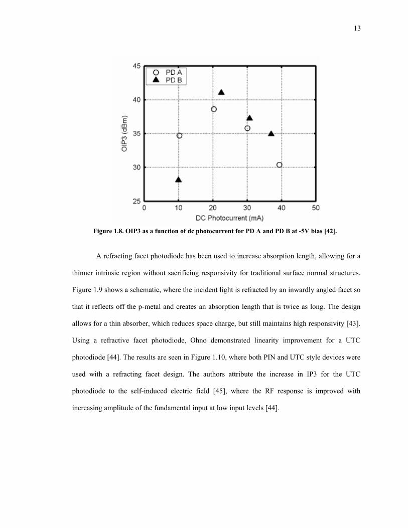
(OIP3) of 42dBm near 20mA [42]. Photodiode linearity presents an important figure of merit that
we will focus on for a large part of this dissertation.
13
Figure 1.8. OIP3 as a function of dc photocurrent for PD A and PD B at -5V bias [42]. A refracting facet photodiode has been used to increase absorption length, allowing for a
thinner intrinsic region without sacrificing responsivity for traditional surface normal structures.
Figure 1.9 shows a schematic, where the incident light is refracted by an inwardly angled facet so
that it reflects off the p-metal and creates an absorption length that is twice as long. The design
allows for a thin absorber, which reduces space charge, but still maintains high responsivity [43].
Using a refractive facet photodiode, Ohno demonstrated linearity improvement for a UTC
photodiode [44]. The results are seen in Figure 1.10, where both PIN and UTC style devices were
used with a refracting facet design. The authors attribute the increase in IP3 for the UTC
photodiode to the self-induced electric field [45], where the RF response is improved with
increasing amplitude of the fundamental input at low input levels [44].

14
Figure 1.9. Schematic cross-sectional view of RFPD [43].
Figure 1.10. Dependence of three tone IP3 for pin-RFPD and UTC-RFPD on average photocurrent
at 3V bias [44].
1.3.4 Design and Considerations
Now that we have briefly discussed photodiode types and some of their characteristics,
we will outline the general considerations we will focus on for our design. One tradeoff in
photodiode design is bandwidth and responsivity. The device transit time, the time it takes a

15
carrier to cross the depletion layer, is related to the depletion width, W, and carrier velocity,
, for a typical PIN photodiode via [3]:
Competing with this process is the capacitance, which can be described by [46]:
where ε is the dielectric constant and A is the device area. From (1.11) and (1.12) and the fact that
responsivity is related to the depletion volume for a surface normal device, we are presented with
a number of tradeoffs.
Despite the bandwidth, transit-time and efficiency tradeoff, device miniaturization and
improvements in layer structures have allowed high speed surface normal diodes with good
responsivity. A 3dB bandwidth of 110GHz with a back illuminated PIN PD was achieved by
using a matched resistor to reduce the effective load to 25Ω, which increased the RC -bandwidth
[47]. Another solution is to use a resonant cavity enhanced structure, where mirrors are at the top
and bottom of the structure to create multi-pass absorption and increase quantum efficiency [48].
This technique is similar to the refracting facet structure detailed in 1.3.3 where the light is
reflected off the p-metal so that the absorption length is increased [49].
A traveling wave photodetector (TWPD) may be used to synchronize the phase of
photocurrents generated at different location so that they add in phase [50-55]. The TWPD is a
distributed structure in that the photogenerated electrical signal propagates along the electrical
contacts, where the characteristic impedance is matched to the external microwave circuit [56].
The benefit of this device is that the TWPD can be long in order to obtain high efficiency without
significantly compromising bandwidth [51]. The TWPD design can be applied to discrete
detectors that are surface normal or waveguide photodiodes, however waveguide photodiodes are
used more frequently since the design is easier to implement. A similar type of structure uses
16
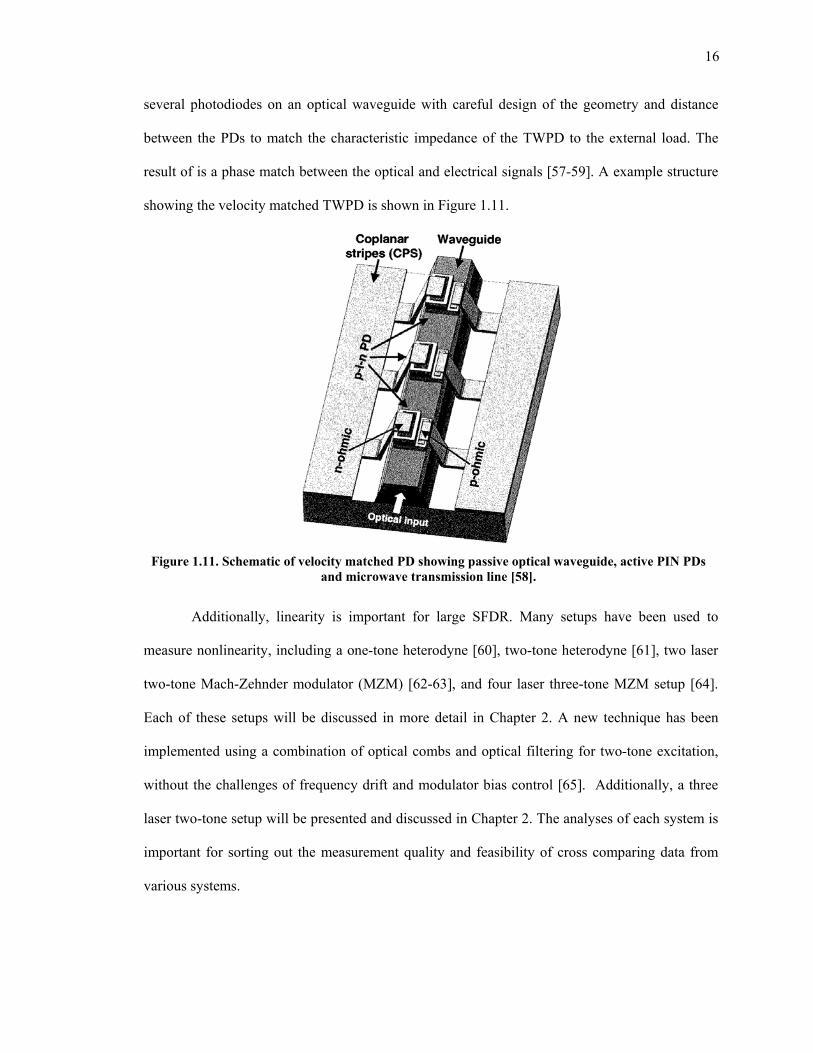
several photodiodes on an optical waveguide with careful design of the geometry and distance
between the PDs to match the characteristic impedance of the TWPD to the external load. The
result of is a phase match between the optical and electrical signals [57-59]. A example structure
showing the velocity matched TWPD is shown in Figure 1.11.
Figure 1.11. Schematic of velocity matched PD showing passive optical waveguide, active PIN PDs
and microwave transmission line [58].
Additionally, linearity is important for large SFDR. Many setups have been used to
measure nonlinearity, including a one-tone heterodyne [60], two-tone heterodyne [61], two laser
two-tone Mach-Zehnder modulator (MZM) [62-63], and four laser three-tone MZM setup [64].
Each of these setups will be discussed in more detail in Chapter 2. A new technique has been
implemented using a combination of optical combs and optical filtering for two-tone excitation,
without the challenges of frequency drift and modulator bias control [65]. Additionally, a three
laser two-tone setup will be presented and discussed in Chapter 2. The analyses of each system is
important for sorting out the measurement quality and feasibility of cross comparing data from
various systems.

17
Figure 1.12. (a) Three-tone IMD3 measurement at 60mA (b) Comparison of Two-Tone and Three-Tone OIP3 (with 3dB correction factor) [66].

18
Ramaswamy et al. used both a two-tone and three-tone system to characterize different
diodes. Their analysis looked at two UTC photodiodes, where one is designed to reduce front-end
saturation and increase linearity using a tapered structure. From Figure 1.12 we can see the
results. The original device which has OIP3 ~39dBm has good agreement between the two
systems. In the case of the second device, with the tapered structure, the OIP3 is 2-3dB less for
the two-tone setup, after the mathematical corrections are made, leaving them to conclude the
three-tone setup is essential in certain situations for measuring OIP3 [66].
There are many device mechanisms that contribute to nonlinearity. Williams et al.
pointed out that at high power conditions, carrier velocities and diffusion constants are functions
of the carrier densities. These parameters will be functions of the carrier densities that are
influenced by space-charge fields, the flow of current in the p-contact modifying the carrier
velocities, scattering, potential drops in the photodiode due to current flow in the external load
resistance, saturation of trap sites, carrier bleaching and carrier density dependent changes to the
carrier acceleration and scattering times [67]. In the case of space-charge induced nonlinearities,
if the dark electric field in the intrinsic region is not high enough over the entire region to saturate
hole and electron velocities, a photogenerated space-charge field will induce carrier velocity
variations. In Figure 1.13, a PIN diode was simulated with constant light equivalent to 1mA and
100µA and the resulted space-charge fields are plotted [67]. Additionally, the second harmonic
power was analyzed over bias voltage to separate the different nonlinear mechanisms. Figure 1.14
shows the result, where at low bias, space-charge dominates (due to the low dark electric field)
and as bias crosses 10V the p-region absorption dominates. The p-region absorption is due to
additional electrons that live long enough in the p-region to enter the intrinsic region. The
nonlinearity is a function of low field carrier mobility, lifetime in the doped material, physical
dimensions, and the p-region doping level [67].

19
Figure 1.13. Calculated space-charge electric field in the intrinsic region at currents of 0.1 (solid) and
1 (dashed) mA, with simulated spot size of 7µm [67].
Figure 1.14. Measured second harmonic power of the 0.95µm PD showing the regimes of importance
for the dominating nonlinear mechanisms [67].
Under saturation the space-charge electric field redistributes the applied field, causing
collapse [68]. In order to avoid this we can adjust the design so as to uniformly illuminate the

20
absorber [69]. One method to accomplish this is by expanding the Gaussian beam so that a small
portion of the light misses the absorbing region, but that the overall profile is more uniform. The
results of this show that compression current can be doubled for the same applied voltage [31].
When the electric field collapses, the field only decreases or increases in certain areas [70]. One
method to relieve this issue and avoid space-charge screening is to use charge compensation so
that a non-uniform electric field is created to counteract the charge-screening [70]. Other
mechanisms that contribute to saturation include thermal [71] and series resistance [72]. Li et al.
showed that for a front illuminated device the lateral resistance dominates saturation, where as for
the backside case the response is determined by space-charge effect, with a saturation current
>400mA for a 100µm diameter partially depleted absorber (PDA) device [73].
Thermal considerations are an important factor when considering photodiode design.
Frequently, thermal failure is observed before current saturation [56]. InP has a fairly low thermal
conductivity (0.68 W/cm/K) and InGaAs is even worse (0.05W/cm/K) [73]. If other materials
could be used in place of InP substrate, such as Si (1.3W/cm/K), SiC (3.6-4.9W/cm/K) [73], or
even diamond, the heat conduction through the substrate can be improved [56]. InGaAs
photodiodes have been transferred to Si substrates using direct semiconductor-to-semiconductor
wafer bonding [74].
1.4 Motivation
The motivation for this work is twofold: first analyze and design a system for
measurement of harmonic and intermodulation distortion; second use the system to characterize
photodiodes in order to better understand how to design high linearity and high power
photodiodes. As can been seen for section 1.3.3, numerous methods have been used to measure
nonlinear distortion in photodiodes. There has been some work that has analyzed these systems
21
[66], but there are still many unanswered questions about how accurately these systems measure
the photodiode nonlinearity and whether data from each can be compared. Once we have a better
understanding of the measurement system and its limitations, we can use this information to
investigate nonlinearity in photodiodes to improve device design for high power high linearity
analog optical links.
Practically, we would like to be able to definitively determine the photodiode distortion
so that we can model the physical mechanisms that are responsible. If our system is measuring
some other distortion, such as from the electrical spectrum analyzer (ESA) or the MZM, we will
not be able to model the photodiode behavior and understand the root causes of the distortion. As
photodiodes push the boundaries for linearity and power, the measurement systems used will near
their limitations due to link component limitations, leaving our knowledge of the photodiode in
question. If we can accurately measure photodiode linearity and model it's behavior using a well
understood system, we can continue moving photodiode technology forward in the quest to rival
electronic components.
1.5 Scope of Dissertation
This dissertation is broken down into two main sections: the linearity measurement
system and device designs for use in high power and high linearity analog optical links. As the
need increases for photodiodes to be more linear, the system on which we measure them becomes
strained at high powers. In order to address the design issues, we must first look at our
measurement system in order to determine if we have the capability to accurately measure the
device metrics (namely OIP3) of our photodiodes. Chapter 2 focuses on an introduction to
photodiode linearity and the various measurement systems used. A new system, a three-laser two
tone setup, is proposed, which successfully calibrates out unwanted MZM nonlinearities. The

22
three-laser two-tone setup is then experimentally and analytically characterized. Since there is
more than one way to measure nonlinearity, it is important to look at alternative measurement
systems. A four-laser three-tone setup and one and two-tone heterodyne setups are experimentally
compared, using mathematical relationships to determine whether the setups can be used to
compare OIP3 data between one another. Although we may have a useful measurement setup, it
is important to identify any discrepancies that may occur between setups that are used to measure
photodiodes in the research field.
Chapter 3 focuses on the study of two PIN waveguide photodiodes. The diodes have
almost identical structures including intrinsic layer thickness, but different absorber thicknesses
and lengths. The purpose of this study is to look at two PIN WGPD in order to investigate the
tradeoffs between bandwidth, power handling capability, and linearity. The original device is
designed for 20GHz bandwidth, while the second is designed for half the bandwidth but higher
power dissipation capability and a more uniform absorption distribution. Specifically, we analyze
both diodes using thermal and electrical device simulation to look at saturation and heating
properties. Additionally, the bandwidth, saturation, linearity and power dissipation are
experimentally measured. The devices are compared and contrasted to understand the benefits
from reducing the optical overlap factor and lengthening the device, with the tradeoff of a lower
bandwidth. Finally, an analytic model first used in [74] is used to characterize one of the devices
and look at what the approximate values of each circuit component need to be in order to improve
OIP3 for future devices.
Chapter 4 presents a novel photodiode structure. The device combines a modified UTC
layer structure with a directional coupled waveguide photodiode in an effort to alleviate the large
current densities inherent in waveguide style photodiodes. The baseline device is characterized
through thermal and electrical simulation and then experimentally. Additional devices were also
produced with variations on the MMI and device width. We will look at the measured and

23
expected bandwidth and thermally model the devices to look at their power handling capabilities
based on the device geometry. We will also look at responsivity and OIP3, using an analytical
model to show the relationship between the two for each variation at low frequency.
Finally, Chapter 5 summarizes the key contributions from each of the previous chapters
and presents future work.

24
1.6 References
[1] B. B. Baker and E. T. Copson, The Mathematical Theory of Huygens' Principle New York, NY: Chelsea, 1987, pp. 1.
[2] S. E. Thompson and S. Parthasarathy, "Moore's law: the future of Si microelectronics,"
Materials Today, vol. 9, no. 6, pp. 20-25 (2006).
[3] C. H. Cox III, Analog Optical Links New York, NY: Cambridge, 2004, pp. 1-164.
[4] D. Derickson, Fiber Optic Test and Measurement Upper Saddle River, NJ: Prentice-Hall, 1998, pp. 12.
[5] R. A. Minasian, "Photonic Signal Processing of High-Speed Signals Using Fiber Gratings," Optical Fiber Technology, vol. 6, pp. 91-108 (2000).
[6] A. J. Seeds and K. J. Williams, "Microwave Photonics," Journal of Lightwave Technology, vol. 24, no. 12, pp. 4628-4641 (2006).
[7] B. Jalali and Y. M. Xie, "Optical folding-flash analog-to-digital converter with analog encoding," Optics Lett., vol. 20, no. 18, pp. 1901-1903 (1995).
[8] H. F. Taylor, "An Optical Analog-to-Digital Converter - Design and Analysis," IEEE J. Quantum Electron., vol. 15, no. 4, pp. 210-216 (1979).
[9] W. S. Chang, RF Photonic Technology in Optical Fiber Links, New York, NY: Cambridge, 2002, pp. 1-18.
[10] J. Capmany and D. Novak, "Microwave photonics combines two worlds," Nature Photonics, vol. 1, pp. 319-330 (2007).
[11] C. H. Cox III, G. E. Betts, and L. M. Johnson, "An Analytic and Experimental Comparison of Direct and External Modulation in Analog Fiber-Optic Links," IEEE Trans. on Micro. Theory Tech.,
[12] E. Ackerman, S. Wanuga, D. Kasemset, A. S. Daryoush, and N. R. Samant, "Maximum Dynamic Range Operation of a Microwave External Modulation Fiber-Optic Link," IEEE Trans. on Micro. Theory Tech., vol. 41, no. 8. pp. 1299-1306 (1993).
[13] L. T. Nichols, K. J. Williams, and R. D. Esman, "Optimizing the Ultrawide-Band Photonic Link," IEEE Trans. on Micro. Theory. Tech., vol. 45, no. 8, pp. 1384-1389 (1997).
[14] T. R. Clark, M. Currie, and P. J. Matthews, "Digitally Linearized Wide-Band Photonic Link," J. Lightw. Technol., vol. 19, no. 2, pp. 172-179 (2001).

25
[15] A. Karim and J. Davenport, "Low Noise Figure Microwave Photonic Link," IEEE MTT-S Int. Micro. Symposium 2007,pp. 1519-1522 (2007).
[16] C. Cox III, E. Ackerman, R. Helkey, and G. E. Betts, "Techniques and Performance of Intensity-Modulation Direct-Detection Analog Optical Links," IEEE Trans. on Micro. Theory Tech., vol. 45, no. 8, pp. 1375-1383 (1997).
[17] D. J. M. Sabido IX, L. G. Kazovsky, "Dynamic Range of Optically Amplified RF Optical Links," IEEE Trans. on Micro. Theory Tech., vol. 49, no. 10, pp. 1050-1055 (2001).
[18] E. I. Ackerman and C. H. Cox III, "The Effect of a Mach-Zehnder Modulator's Traveling-Wave Electrode Loss on a Photonic Link's Noise Figure," Int.Topical Meet. on Micro. Photon., pp. 321-324 (2003).
[19] G. L. Li, T. G. B Mason and P. K. L. Yu, "Analysis of segmented traveling-wave optical modulators," J. Lightw. Technol., vol. 22, no. 7, pp. 1789-1796 (2004).
[20] B. G. Streetman and S. Banerjee, Solid State Electronic Devices, Upper Saddle River, NJ: Prentice Hall, 2000, pp. 388.
[21] V. J. Urick, A. S. Hastings, J. D. McKinney, P. S. Devgan, C. Sunderman, J. F. Diehl, K. Colladay and K. J. Williams, “Photodiode Linearity Requirements for Radio-Frequency Photonics and Demonstration of Increased Performance Using Photodiode Arrays,” 2008 Int. Meeting Microwave Photonics Digest, pp. 86-89, Oct. 2008.
[22] M. Shur, Physics of Semiconductor Devices, Englewood Cliffs, NJ: Prentice-Hall, 1990, pp. 503.
[23] R. G. Drigger, Encyclopedia of optical engineering, vol. 2, New York, NY: Marcel Dekker, 2003, pp. 1904.
[24] H. Bayhan and S. Ozden, "Measurement and Comparison of Complex Impedance of Silicon p-i-n Photodiodes at Different Temperatures," Semiconductors, vol. 41, no. 3, pp. 353-356 (2007).
[25] S. S. Tan, C. Y. Liu, Y. Jiang, D. Lin, and K. Y. J. Hsu, "Spectral response design of hydrogenated amorphous silicon p-i-n diodes for ambient light sensing," App. Phys. Lett., vol. 94, pp. 171103-171103-3 (2009).
[26] S. N. Mohammad and H. Morkoc, "Progress and Prospects of Group-III Nitride Semiconductors," Progress in Quantum Elect., vol. 20, no. 5, pp. 361-525 (1996).
[27] J. C. Lin, Y. K. Su, S. J. Chang, W. H. Lan, K. C. Huang, W. R. Chen, C. Y. Huang, W. C. Lai, W. J. Lin and Y. C. Cheng, "High responsivity of GaN p-i-n photodiode by using low-temperature interlayer," App. Phys. Lett., vol. 91, pp. 173502-173502-3 (2007).Figur

26
[28] G. Y. Xu, A. Salvador, W. Kim, Z. Fan, C. Lu, H. Tang, H. Morkoc, G. Smith, M. Estes, B. Goldenber, W. Yang and S. Krishnankutty, "High speed, low noise ultraviolet photodetectors based on GaN p-i-n and AlGaN(p)-GaN(i)-GaN(n) structures," App. Phys. Lett., vol. 71, no. 15, pp. 2154-2156 (1997).
[29] N. Biyikli, I. Kimukini, O. Aytur, and E. Ozbay, "Solar-Blind AlGaN-Base p-i-n Photodiodes With Low Dark Current and High Detectivity," IEEE Photon. Technol. Lett., vol. 16, no. 7, pp. 1718-1720 (2004).
[30] M. Dentan and B. De Cremoux, "Numerical Simulation of Nonlinear Response of a p-i-n Photodiode Under High Illumination," J. Lightw. Technol., vol. 8, no. 8, pp. 1137-1144 (1990).
[31] G. A. Davis, R. E. Weiss, R. A. LaRue, K. J. Williams, and R. D. Esman, "A 920-1650-nm High-Current Photodetector," IEEE Photon Technol. Lett., vol. 8, no. 10, pp. 1373-1375 (1996).
[32] N. Shimizu, N. Watanabe, T. Furata and T. Ishibashi, "High-Speed InP/InGaAs Uni-Traveling-Carrier Photodiodes with 3-dB Bandwidth over 150GHz," 55th Annual Device Research Conf. Digest 1997 (Fort Collins, CO), pp. 164-165 (June 1997).
[33] T. Ishibashi, N. Shimizu, S. Kodama, H. Ito, T. Nagatsuma and T. Furuta, "Uni-Traveling-Carrier Photodiodes," Ultrafast Electronics and Optoelectronics Technical Digest 1997, pp. 83-87.
[34] E. Rouvalis, C. C. Renaud, D. G. Moodie, M. J. Robertson and A. J. Seeds, "Traveling-wave Uni-Traveling Carrier Photodiodes for continuous wave THz generation," Opt. Express, vol. 18, no. 11, pp. 11105-11110 (2010).
[35] T. Ishibashi, "High speed heterostructure devices," in Semiconductors and Semimetals. San Diego, Ca: Academic, 1994, vol. 41, ch. 5, p. 333.
[36] H. Ito, T. Furato, S. Kodama and T. Ishibashi, "Zero-bias high-speed and high-output-voltage operation of cascade-twin unitravelling-carrier photodiode," Electron. Lett., vol. 36, no. 24, pp. 2034-2036 (2000).
[37] A. Beling and J. C. Campbell, "InP-Base High-Speed Photodetectors," J. Lightw. Technol., vol. 27, no. 3, oo, 343-355 (2009).
[38] Y.-S. Wu, and J.-W. Shi, "Dynamic analysis of high-power and high speed near-ballistic unitraveling carrier photodiodes at w-band," IEEE Photon. Technol. Lett., vol. 20, no. 13, pp. 1160-1162 (2008).
[39] D.-H. Jun, J.-H. Jang, I. Adesida, and J.-I. Song, "Improved efficiency-bandwidth product of modified uni-traveling carrier photodiode structures using an undoped photo-absorption layer," Jpn. J. Appl. Phys., vol. 45, no. 4B, pp. 3475-3478 (2006).

27
[40] X. Wang, N. Duan, H. Chen, and J. C. Campbell, "InGaAs-InP Photodiodes With High Responsivity and High Saturation Power," IEEE Photon. Technol. Lett., vol. 19, no. 16, pp. 1272-1274 (2007).
[41] H. Ito, T. Ito, Y. Muramoto, T. Furata, and T. Ishibashi, "Rectangular Waveguide Output Unitraveling-Carrier Photodiode Module for High-Power Photonic Millimeter-Wave Generation in the F-Band," J. Lightw. Technol., vol. 21, no. 12, pp. 3456-3462 (2003).
[42] J. Klamkin, Y.-C. Chang, A. Ramaswamy, L. A. Johansson, J. E. Bowers, S. P. DenBaars, and L. A. Coldren, "Output Saturation and Linearity of Waveguide Unitraveling-Carrier Photodiodes," J. Quantum Electon., vol. 44, no. 4, pp. 354-359 (2008).
[43] H. Fukano, Y. Muramoto, and Y. Matsuoka, "Edge-Illuminated Refracting-Facet Photodiode with Large Bandwidth and High Output Voltage," Jpn. J. Appl. Phys., vol. 39, no. 4B, pp. 2360-2363 (2000).
[44] T. Ohno, H. Fukano, Y. Muramot, T. Ishibashi, and Y. Doi, "Measurement of Intermodulation Distortion in a Unitraveling-Carrier Refracting-Facet Photodiode and a p-i-n Refracting-Facet Photodiode," IEEE Photon. Technol. Lett., vol. 14, no. 3, pp. 375-377 (2002).
[45] D. K. Cheng, "Capacitance and capacitors," in Field and Wave Electromagnetics, 2nd ed., New York, NY: Addison-Wesley, 1992, pp. 123.
[46] N. Shimizu, N. Watanabe, T. Furuta and T. Ishibashi, "Improved Response of Uni-Traveling-Carrier Photodiodes by Carrier Injection," Jpn. J. Appl. Phys., vol. 37, no. 3B, pp. 1424-1426 (1998).
[47] Y.-G. Wey, K. Giboney, J. Bowers, M. Rodwell, P. Silvestre, P. Thiagarajan, and G. Robinson, "110-GHz GaInAs/InP Doubler Heterostructure p-i-n Photodetectors," J. Lightw. Technol., vol. 13, no. 7, pp. 1490-1499 (1995).
[48] I. Kimukin, N. Biyikli, B. Butun, O. Aytur, S. M. Unlu, and E. Ozbay, "InGaAs-Based High-Performance p-i-n Photodiodes," IEEE Photon. Technol. Lett., vol. 14, no. 3, pp. 366-368 (2002).
[49] H. Fukano and Y. Matsuoka, "A Low-Cost Edge-Illuminated Refracting-Facet Photodiode Module with Large Bandwidth and High-Responsivity," J. Lightw. Technol., vol. 18, no. 1, pp. 79-83 (2000).
[50] K. S. Giboney, M. J. W. Rodwell, and J. E. Bowers, "Traveling-Wave Photodetectors," IEEE Photon. Technol. Lett., vol. 4, no. 12, pp. 1363-1365 (1992).
[51] K. S. Giboney, M. J. W. Rodwell, and J. E. Bowers, "Traveling-Wave Photodetector Theory," IEEE Trans. Microw. Theory Tech., vol. 45, no. 8, pp. 1310-1319 (1997).

28
[52] K. S. Giboney, R. L. Nagarajan, T. E. Reynolds, S. T. Allen, R. P. Mirin, M. J. W. Rodwell, and J. E. Bowers, "Travelling-Wave Photodetectors with 172-GHz Bandwidth and 76-GHz Bandwidth-Efficiency Product," IEEE Photon. Technol. Lett., vol. 7, no. 4, pp. 412-414 (1995).
[53] A. Stohr, A. Malcoci, A. Sauerwald, I. C. Mayorga, R. Gusten, and D. S. Jager, "Ulta-Wide-Band Traveling-Wave Photodetectors for Photonic Local Oscillators," J. Lightw. Technol., vol. 21, no. 12, pp. 3062-3070 (2003).
[54] V. M. Hietala, G. A. Vawter, T. M. Brennan, and B. E. Hammons, "Traveling-Wave Photodetectors for High-Power, Large-Bandwidth Applications," IEEE Trans. Microw. Theory Tech., vol. 43, no. 9, pp. 2291-2298 (1995).
[55] Y.-J. Chiu, S. B. Fleischer, and J. E. Bowers, "High-Speed Low-Temperature-Grown GaAs p-i-n Traveling-Wave Photodetector," IEEE Photon. Technol. Lett., vol. 10, no. 7, pp. 1012-1014 (1998).
[56] J. C. Campbell, "Advances in Photodetectors," in Optical Fiber Telecommunications V: Components and subsystems, vol. 1, Burlington, MA: Elsevier, 2008, pp. 223.
[57] L. Y. Lin, M. C. Wu, T. Itoh, T. A. Vang, R. E. Muller, D. L. Sivco, and A. Y. Cho, "High-Power High-Speed Photodetectors-Design, Analysis, and Experimental Demonstration," IEEE Trans. Microw. Theory Tech., vol. 45, no. 8, pp. 1320-1331 (1997).
[58] M. S. Islam, S. Murthy, T. Itoh, M. C. Wu, D. Novak, R. B. Waterhouse, D. L. Sivco, and A. Y. Cho, "Velocity-Matched Distributed Photodetectors and Balanced Photodetectors with p-i-n Photodiodes," IEEE Trans. Microw. Theory Tech., vol. 49, no. 10, pp. 1914-1920 (2001).
[59] Y. Hirota, T. Ishibashi, and H. Ito, "1.55-µm Wavelength Periodic Traveling-Wave Photodetector Fabricated Using Unitraveling-Carrier Photodiode Structures," J. Lightw. Technol., vol. 19, no. 11, pp. 1751-1758 (2001).
[60] R.D. Esman and K. J. Williams “Measurement of Harmonic Distortion in Microwave Photodetectors,” IEEE Photon. Technol. Lett., vol. 2, no. 7. pp 502 - 504, Jul. 1990.
[61] D. C. Scott, T. A. Vang, J. Elliott, D. Forbes, J. Lacey, K. Everett, F. Alvarez, R. Johnson, A. Krispin, J. Brock, L. Lembo, H. Jiang, D. S. Shin, J. T. Zhu and P. K. L. Yu, “Measurement of IP3 in p-i-n photodetectors and proposed performance requirements for RF fiber-optic links,” IEEE Photon. Technol. Lett., vol. 12, pp. 422-424 (2000).
[62] H. Jiang, D. S. Shin, G. L. Li, T. A. Vang, D. C. Scott, and P. K. L. Yu, “The frequency behavior of the third-order intercept point in a waveguide photodetector,” IEEE Photon. Technol. Lett., vol. 12, pp. 540-542 (2000).
[63] A. Beling, H. Pan, H. Chen and J. C. Campbell, “Linearity of modified uni-traveling carrier photodiodes,” J. Lightw. Technol., vol. 26, pp. 2373-2378 (2008).
29
[64] A. Ramaswamy, N. Nunoya, M. Piels, L. A. Joahansson, L. A. Coldren, J. E. Bowers, A. S. Hastings, K. J. Williams, and J. Klamkin, "Experimental Analysis of Two Measurement Techniques to Characterize Photodiode Linearity," Int. Topical Meeting on Microwave Photonics (MWP 2009), Valencia, Spain, Oct. 2009.
[65] J. D. McKinney, D. E. Leaird, A. S. Hastings, A. M. Weiner, and K. J. Williams, "Optical Comb Source and High-Resolution Optical Filtering for Measurement of Photodiode Harmonic Distortion," J. Lightw. Technol., vol. 28, no. 8, pp. 1228-1235 (2010).
[66] A. Ramaswamy, N. Nunoya, K. J. Williams, J. Klamkin, M. Piels, L. A. Johansson, A. S. Hastings, L. A. Coldren, and J. E. Bowers, "Measurement of intermodulation distortion in high-linearity photodiodes," Opt. Express, vol. 18, no. 3, pp. 2317-2324 (2010).
[67] K. J. Williams, R. D. Esman, and M. Dagenais, "Nonlinearities in p-i-n Microwave Photodetectors," J. Lightw. Technol., vol. 14, no. 1, pp. 84-96 (1996).
[68] K. J. Williams, R. D. Esman, and M. Dagenais, "Effects of High Space-Charge Fields on the Response of Microwave Photodetectors," IEEE Photon. Technol. Lett., vol. 6, no. 5, pp. 639-641 (1994).
[69] K. J. Williams and R. D. Esman, "Design Considerations for High-Current Photodetectors," J. Lightw. Technol., vol. 17, no. 8, pp. 1143-1454 (1999).
[70] K. J. Williams, "Comparisons between dual-depletion-region and uni-travelling-carrier p-i-n photodetectors," IEEE Proc. Optoelectron., vol. 149, no. 4, pp. 131-137 (2002).
[71] N. Duan, X. Wang, N. Li, H.-D. L, and J. C. Campbell, "Thermal Analysis of High-Power InGaAs-InP Photodiodes," J. Quantum Electron., vol. 42, no. 12, pp. 1255-1258 (2006).
[72] X. Li, N. Li, S. Demiguel, J. C. Campbell, D. Tulchinsky, and K. J. Williams, "A Comparison of Front- and Backside-Illuminated High-Saturation Power Partially Depleted Absorber Photodetectors," J. Quantum. Electron., vol. 40, no. 9, pp. 1321-1325 (2004).
[73] D. A. Tulchinsky, K. J. Williams, A. Pauchard, M. Bitter, Z. Pan, L. Hodge, S. G. Hummel, and Y. H. Lo, "High-power InGaAs-on Si pin RF photodiodes," Electron. Lett., vol. 39, no. 14, pp. 1084-1086 (2003).
[74] H. Jiang and P. K. L. Yu, “Equivalent circuit analysis of harmonic distortions in photodiode,” IEEE Photon. Technol. Lett. vol. 10, pp. 1608–1610 (Nov. 1998).

30
Chapter 2 Nonlinearity and Measurement Systems
2.1 Introduction
The spurious free dynamic range of analog fiber-optic links is closely tied to the linearity
of the transmitter and the photodiode. As power increases, the linearity performance of the
photodiode progressively becomes a limitation. When two RF tones coming from two modulated
optical signals are input into the detector many spurious signals arise. Particularly third-order
intermodulation distortions (IMD3) are important due to the fact that they appear very close to the
fundamental signals and cannot be easily removed by filters [1]. The measurement of IMD3 and
the third-order intercept point (IP3) are essential to understanding the nonlinearities caused by
photodiodes. IP3 is the intersection of the extrapolation of IMD3 and output fundamental RF
power, Pf. Additionally the mixing of the two tones will create second order intermodulation
distortion (IMD2) that is also of interest. The second order intercept (IP2) limits broad-band
dynamic range in the same way IP3 limits narrow-band dynamic range [2]. As the need for
detectors with higher linearity increases with the desire for larger link spurious-free dynamic
range, the need for more accurate and larger measurement range is essential to meeting this goal.
In order to accurately perform the measurement all other nonlinearities contributed by equipment
must be minimized or calibrated out.
We intend to investigate various nonlinearity measurement setups for this chapter. First,
we need to assess the current output third order intercept point setup. The two-laser two-tone
setup will be described in detail as well as the problems we face when making photodiode
measurements. Next a new three-laser two-tone setup will be presented as a solution to the issues

31
faced with the original setup. Our main goal is to understand the new setup by experimentally and
analytically finding its limitations for measuring OIP3. Finally, we will discuss two other types of
setups that have been used to measure OIP3: one and two-tone heterodyne and the four-laser
three-tone Mach-Zehnder setups. The purpose of analyzing these setups is to investigate whether
these setups can be used interchangeably, namely do they give the same OIP3 for the same
photodiode based on the accepted mathematical relationships.
2.2 Background and Motivation
2.2.1 Introduction to IP3
First we will discuss the creation of nonlinearities in a photodiode. Figure 2.1 shows the
radio frequency (RF) output representation of the optical signal components for a two tone input.
Assuming we have two input tones ( and ) implanted on a continuous wave (CW) optical
signal, the output will contain the two fundamental tones, shown in black in Figure 2.1, but
additional spurious (red) and intermodulation (blue) tones will also arise due to the inherent
nonlinearities of the photodiode. The second order spurious tones will arise at and , while
the second order intermodulation distortion tones will occur at . The third order harmonic
distortion tones will occur at and , while the third order intermodulation will occur at
and . The intermodulation tones that appear close to the fundamental are
important due to the fact that they cannot be filtered out [1]. The IMD3 is due to the mixing of
two times one fundamental minus the other and has a slope of three in the log-log scale shown in
Figure 2.2.

32
Figure 2.1. RF output representation of optical signal components for a two-tone input to a photodiode, showing fundamentals (black), harmonic distortions (red) and intermodulation
distortions (blue).
Figure 2.2. Fundamental and IMD3 as a function of input RF power.
2.2.2 Importance of IP3 to Modulation Systems
Chapter 1 briefly outlined spurious free dynamic range (SFDR) for an intensity
modulated direct detection (IMDD) link, shown in Figure 2.3. The system consists of a CW laser
input to a Mach-Zehnder modulator (MZM), which is bias controlled and fed with a RF signal.
The output of the MZM is input to the photodiode, which is reverse biased, and the electrical
output is measured on an electrical spectrum analyzer (ESA).
Figure 2.3. An intensity modulated direct detection link.

33
SFDR is the ratio of the power of the fundamental signal to the power of the largest spurious
component in a certain frequency range [3]. The modulator limited signal free dynamic range
(SFDRMOD) can be described by:
where is the modulator IP3 and is the output noise power. Since the SFDR is not
always limited by the modulator, the degradation of SFDR due to the photodiode can be
calculated as:
where is the difference between the IP3 of the modulator and the photodiode. We now see
that if the photodiode nonlinearity is greater than the modulator nonlinearity the SFDR of the link
will be reduced, thereby demonstrating the need to effectively measure photodiode IP3,
characterize nonlinearities, and develop new designs for high linearity photodiodes.
2.3 Measurement Schemes
2.3.1 Two-Tone Heterodyne Setup
The five-laser heterodyne setup can be seen in Figure 2.4. The setup consists of two pairs
of lasers, where the optical offset frequency for each pair is stabilized by mixing the resulting RF
intermodulation tone (λ1/3-λ2/4) with an RF reference signal and running the mixed signal through
a phase-locked loop (PLL) circuit back into the wavelength control for one of the lasers, where
the second laser is at a fixed wavelength. Each output is fed into an optical attenuator and then
combined using a 50/50 optical coupler and combined with a 5th laser used for controlling the DC

34
PD current. The device under test (DUT) is illuminated with the resulting signal and the RF
output signal is measured by an ESA. The modulation index is changed by attenuating each pair
of heterodyned lasers, and adjusting the power of the DC laser (λ5) to compensate. In this setup,
the wavelengths of the lasers must be carefully controlled so that all unwanted optical
intermodulation tones in the RF frequency domain fall outside the bandwidth of the photodiode
under test. The entire setup is fiber spliced where polarization maintaining (PM) fiber is used
throughout to control the polarization. Although a heterodyne setup has been used by [4, 5], it can
be more complicated to work with in order to get the proper fundamental tones. This scheme does
not depend on the linearity of any RF source, but does require the lasers to operate with high
wavelength stability up to high power. Additionally, each pair of lasers need to be closely
matched in wavelength and immune to drifts, while the lasers in each pair are locked to each
other [6]
Figure 2.4. Five laser heterodyne nonlinearity setup.
2.3.2 Two-Tone Mach-Zehnder Modulator (MZM) setup
A simpler and more widely used measurement system is the two-tone MZM setup [1,7].
The setup consists of two of two lasers input into their respective MZM. Two synthesizers

35
provide the RF input to each MZM. The output is combined in a 50/50 coupler and detected at the
DUT. The modulation depth is controlled by increasing or decreasing the RF input to the MZMs.
The setup typically biases the MZM at the quadrature point to minimize HD2 which contributes
to the IMD3 when mixed inside the detector. Additionally, polarizers before the MZMs and
erbium doped fiber amplifiers (EDFA) can be added to boost the optical power input to the
device.
Although biasing at the quadrature reduces the HD2 signal, we cannot be sure the MZM
is not contributing significantly to the IMD3 measured. The quadrature point of the MZM also
changes as a function of time and temperature due to DC bias drift [8]. One of the main issues
with this setup is that the modulators have inherent nonlinearities, in particular, the second order
harmonics (HD2) from the first laser beam, that can mix in the detector with the fundamental RF
tone detected from the second signal and contribute to IMD3. Using this method does not allow
us to distinguish between the nonlinearity created by the MZM and that created by the
photodiode, leaving the IP3 measurement uncertain. To accurately measure the IP3 we will need
to show that the IMD3 due to the MZM (IMD3MZM) can be removed and that the biasing of the
MZM is stable enough to record consistent measurements. In typical setups a polarization
controller is inserted after one of the MZMs in order to control the orthogonality of the laser
beams.
Figure 2.5. Two laser two-tone MZM nonlinearity setup.
36
2.3.3 Three-Laser Two-Tone MZM Setup
An alternative to the two-tone setup presented in 2.3.2 is a three laser two-tone MZM
setup. The setup we present incorporates the technique used in the previous two laser setup [1], as
depicted in Figure 2.6. Two external cavity lasers (ECL) at wavelengths of 1541nm and 1549nm
are input into their respective MZM. A polarization rotator is inserted in front of the MZM to
properly rotate the beam for minimum loss. Two synthesizers shown in Figure 2.6 along with
their respective driver are used to provide the input RF power ( ) to their respective MZM. A
bandpass filter is placed just before the MZM to ensure no second order signals are contributed
by the synthesizers. The output of the MZM is amplified by an EDFA shown in yellow in Figure
2.6. Following the EDFAs are variable optical attenuators (VOA) that will be used to control the
input optical modulation depth to the photodiode ( ). Since both DC power and will
be attenuated with the VOA, a third ECL is needed to maintain the constant input optical power
to the photodiode. The corresponds to the fundamental output power (Pf) seen at the ESA
from the photodiode. The two modulated lasers are combined using a polarizing beam combiner
(PBC) and appropriate polarization rotators to ensure the beams are orthogonal. The purpose of
the PBC is to ensure there will be no optical mixing before combining in the photodiode. The
third ECL also uses an EDFA and VOA for amplification and control of the DC optical power.
The combined first two lasers are coupled with the third using a wavelength division multiplexor
(WDM), “D”, as shown in Figure 2.6. The use of the WDM allows us to combine the DC laser at
a wavelength that is slightly off the first two so that there is not mixing between the lasers.

37
Figure 2.6. Three laser IP3 measurement setup. “A” is a polarization rotator, “B” is an EDFA, “C” is a band pass filter, and “D” is a wavelength division multiplexor (WDM). ECL stands for external
cavity laser, DVR for driver, PM for optical power meter, VOA for variable optical attenuator, PBC for polarizing beam combiner, DUT for device under test and ESA for electrical spectrum analyzer.
2.3.4 Four-Laser Three-Tone MZM Setup
The final setup that has also been used [6, 9, 10], is a three-tone setup. The setup, shown
in Figure 2.7, is similar to that described in 2.3.3, but adds an additional ECL and MZM to the
setup. The purpose of this setup is to measure the IMD3 resulting from the combination of three
different input tones ( , , ), which gives third order intermodulation distortion at
, , , and ( , where the first three are close to the
fundamental. By measuring the IMD3 as a function of three different input tones, the second
order nonlinearity due to the MZM is completely removed [6]. The three-tone case is not
equivalent to the two-tone case, therefore a mathematical relationship is usually used to compare
measurements between devices [9]. The relationship between these setups will be described later
in detail.

38
Figure 2.7. Four laser three-tone MZM nonlinearity setup.
2.4 Three-Laser Two-Tone System
2.4.1 Introduction
The purpose of this section is to experimentally and analytically characterize the setup
described in 2.3.3. The three laser two-tone nonlinearity setup will first be used to measure the
second and third order intercept points. Next the MZM nonlinearities will be investigated.
Finally, the setup will be mathematically analyzed and the limits will be discussed.
2.4.2 Experiment 1: Second and Third Order Intercept Measurement
Initially the measurement was designed to include a fair amount of modulator
nonlinearity in order to distinguish the different IMD3 tones. To do this we used a large value for
at the synthesizers. For a given value of the RF component of the intensity modulated
output of the MZM in log scale is:
where x denotes the first or second input frequency. When the VOA is used to attenuate the
by a factor of Δ the value of each coefficient (A, B, C…) will decrease at the same factor. The

39
HD2 due to the MZM of will mix with the fundamental of inside the photodiode to generate
IMD3MZM. The change in IMD3MZM in log scale will be:
Equation (2.4) shows that with a decrease in fundamental RF power by the amount of Δ, the
contribution of IMD3 due to the MZMs should change with a slope of two with respect to
fundamental RF power, Pf, in the log scale.
As the measurement is made the results should contain both contributions. Hayes et al.
determined the slope of IMD3 due to the photodiode should be three [11]. For instance, for the
IMD3 term due to mixing of and tones at the photodiode, as each tone is reduced
by 1dB, the IMD3 will be reduced by 3dB (2dB from tone and 1 dB from tone). In the
beginning, when the measured RF fundamental tone, , is small, the IMD3MZM (slope = 2)
dominates; as increases, the IMD3 from the photodiode (IMD3PD) will dominate because it is
increasing at a faster rate than IMD3MZM. Therefore, the IMD3 curve should indicate a knee point
at which IMD3 will change from a slope of two to a slope of three as is increased. After the
two regimes have been distinguished, the IMD3PD, with a slope of three, can be extrapolated with
to find the intercept and determine the IP3 as in previous measurements [1]. The output IP3
(OIP3) which is the value of output power at the intercept can be calculated as according to [12]:
Additionally, the second order intermodulation (IMD2) will be measured at ,
where we will expect a slope of two. The IMD2 will not contain contributions from the
modulators since there is no mixing of the signals prior to the photodiode and only and
are of concern. The IMD2 can then be extrapolated with the fundamental to give a value for the
output second order intercept point (OIP2) and is calculated according to:

40
A PIN InGaAs/InP waveguide photodiode (PD) was used for the measurement test. The
PD was a 5µm width by 55µm length device with a 0.32µm intrinsic region. The PD has a
maximum responsivity around 0.9A/W but was measured at about half the maximum
responsivity for ease of measurement and to ensure stable current throughout the measurement.
The measurement was made at frequencies 1.1GHz and 1.2GHz for and respectively, with
10dBm , 11.5dBm total input optical power, with bias voltage ( ) of 4V, and 5.8mA
photocurrent.
Figure 2.8. Measurement of OIP2 and OIP3 showing IMD contributions from MZM
and DUT distinguished by fitted curves showing appropriate slopes for each.
The results in Figure 2.8 indicate a knee point in the IMD3 data that corresponds to the
change in slope from two to three; a slope of two is measured for IMD2. In the Figure 2.8 we can
see that as predicted the slope at lower input RF values is due to the intermodulation from the
MZM, but that as increases, the slope shifts to three for IMD3 as the photodiode nonlinearity
y = 2.014x - 50.71
y = 2.990x - 64.84
y = 2.045x - 74.50-120
-100
-80
-60
-40
-20
0
20
40
60
-20 0 20 40
Out
put R
F Po
wer
(dB
m)
Output Fundamental RF Power (dBm)
FundamentalIMD2IMD3
Knee Point
OIP3 = 32.6 dBm
OIP2 = 50.0 dBm

41
begins to dominate. On the upper end, the IMD3 measurement is limited by a number of factors
that will be discussed next.
2.4.3 Experiment II: Investigating the MZM Nonlinearity
The second experiment investigates the nonlinearities contributed by the MZM to IMD3.
The purpose of this is to analyze how the MZM imposes limitations on the dynamic range.
Looking at the intrinsic properties of a single modulator and starting with a two-tone input as in
[10]:
the transfer function can be expanded into a Taylor series:
where is the nth derivative of T at and is the input RF voltage that can be related to
. The IMD3MZM in equation (2.4) can be related to the power of the intermodulation term
which is a function of and is defined as [13]:
Equation (2.9) shows that as increases the resulting intermodulation also increases which
means so does IMD3MZM. We measure IMD3 as a function of Pf for different values of to
determine where the MZM must be operated so that the IMD3MZM is suppressed below the noise
floor of the ESA (NFESA). In addition, IMD3's are measured at various MZM biasing points,
quadrature and off quadrature, to assess the effects of the MZM bias on the IMD3MZM.
The first experiment varies to the MZM by changing the output at the synthesizer.
The to the MZM corresponds to 16dBm, 10dBm and 7dBm for test 1, test 2 and test 3
respectively. Figure 2.9 shows the results, where the blue data corresponds to the maximum

42
and the red to the lowest . We can see that as is decreased the resulting IMD3MZM is
reduced. As the IMD3MZM is reduced the IMD3 due to the device remains along the same trend
line as expected. The data allows us to conclude that the to the MZM has no affect on the
IMD3PD, but does affect the ability to measure lower values for the device by contributing to the
IMD3MZM signal. In other words, in previous measurement setups [1] without knowing the exact
contribution of IMD3MZM the results may have been affected by this nonlinearity even when
employing minimum HD2, by biasing at the quadrature. Now that we have been able to analyze
the effects of to the MZM, the next step is to look at the varying of bias to see if biasing at
the quadrature also has a significant effect on the results in the present setup.
Figure 2.9. Measurement showing variation of input RF power to the MZM.
y = 3x - 61.73
-140
-130
-120
-110
-100
-90
-28 -23 -18 -13 -8
PD O
utpu
t RF
Pow
er (d
Bm
)
Output Fundamental RF Power (dBm)
IMD3 PD Test1IMD3 PD Test2IMD3 PD Test3IMD3 MZM Test1IMD3 MZM Test2
IMD3MZM
IMD3MPD

43
Figure 2.10. Effects on IMD3 for MZM biasing test with varying amounts of HD2 suppression.
The second investigation we performed explored the effects of modulator bias. If the
MZM is not biased at the quadrature point we should expect to see this reflected in the IMD3MZM
as previous papers have stated that HD2 due to the MZM contributes to IMD3[1]. In Jiang et al.,
the MZMs were biased at the quadrature point to minimize HD2. The first test performed biased
the MZM at the quadrature point provided 60dB suppression of HD2 below . Figure 2.10
shows the result in red with the contributions to IMD3 from both the PD and the MZM indicated
on the graph. The IMD3MZM limits the floor to ~-115dBm. If the argument stated in previous
papers holds [1], the biasing of the MZM off the quadrature should increase the contribution of
IMD3MZM, and thus the measurement floor. The second test allowed for 20dB suppression of
HD2 below . The results in blue are reflected in Figure 2.10 Even with a much larger
contribution of HD2 the effect on IMD3 is minimal. We conclude that biasing at the quadrature
point to achieve large HD2 suppression does not significantly affect the measurement of IMD3.
The results from examining the nonlinearities contributed by the MZM and equation (2.9)
-125
-120
-115
-110
-105
-100
-95
-90
-85
-30 -25 -20 -15
Out
put R
F Po
wer
(dB
m)
Output Fundamental RF Power (dBm)
IMD3 PD at quadIMD3 PD off quadIMD3 MZM at quadIMD3 MZM off quad
IMD3MZM IMD3PD

44
suggest that to the MZM has a direct relationship to the measurement of IMD3. On the other
hand, biasing the MZM at the quadrature shows little improvement in IMD3MZM. Next we
characterize the setup analytically.
2.4.4 Analytical Characterization
We will begin with Figure 2.6 in 2.3.3, which is the three laser two-tone nonlinearity
measurement setup. In our analysis we will assume the MZMs are almost identical. We define the
transfer function of a modulator as:
Since the device cannot be guaranteed to be biased at we will define the modulator input as:
where the DC bias is off by which is a ratio of the offset to . Δ implies that there will be
some second order components created in the modulator. Next we expand (2.10) after substituting
in (2.11):
We assume that Δ<<1, and use a first order small-signal approximation for sine and
cosine functions. Additionally we assume , that the 4th and 5th powers are negligible, the
fundamental is linear and that the modulator DC output does not depend on . Our modulator
output is then:

45
Next we calculate the total link. In each arm the optical power is:
where , is the laser optical power, is the intrinsic insertion loss for the
modulator, polarizer, EDFA and optical attenuator and is the gain of the EDFA and α is the
optical attenuation set through the optical attenuator. We assume that the gain of the EDFA is
held constant and we only change the attenuation through α. The two arms are combined in
intensity with a polarizing beam combiner (PBC) to give:
where is the insertion loss of the PBC and we are assuming that there is equal insertion loss
to each arm. The third arm consists only of DC optical power and is defined as:
where is now the insertion loss of the EDFA and the optical attenuator, is the gain of the
EDFA and β is the attenuation of the optical attenuator. Next this can be combined with the
previous result using a wavelength division multiplexer (WDM) where the input to the detector
becomes:
where is the insertion loss of the WDM and any additional loss before the detector. In our
measurement we maintain a constant DC input power where we assume as and are lowered
is increased so that:

46
From (2.17) we can calculate our x-axis variable which will be the equivalent input RF power.
This variable will be defined by converting the input optical power that is made up of the
fundamental frequency modulation and assuming a responsivity of 1A/W. From equation (2.17)
we can calculate the photocurrent for the fundamental for a signal :
where . From (2.19a) we can calculate the equivalent input RF power:
The output fundamental RF photocurrent is related by:
where η is the device responsivity and is the quantum efficiency. From all of these we can
calculate the output fundamental RF power as:
From (2.22) we can see that the output fundamental RF power is dependent on the square of the
attenuation. When we attenuate by 1dBm with the optical attenuator, we will see the output RF
power attenuate by 2dBm. For our measurement we are assuming that the fundamental power for
both input frequencies is the same, so that:

47
Next we solve for the distortion contributions. The second order harmonic term generated for
frequency assuming higher order contributions are negligible is:
where we assume the cosine term is negligible. We neglect the ½ term in (2.24) and then
calculate the magnitude of the second order harmonic contribution, including the detector
responsivity:
The second order from the modulator will contain the contribution of that is input into the
detector from the modulator output. Assuming that higher order contributions are negligible we
have:
Now we calculate the intermodulation terms for each. For the detector we have:
We are only concerned with the term and thus have:
where κ is some unknown constant representing the device nonlinearity due to the third order
mixing. Similarly, we will calculate the distortion due to the MZM which is a second order
process.

48
where γ is a constant representing the second order intermodulation mixing. Using (2.28) and
(2.29) we can calculate the output power for both.
Next we look at each output power in log-log scale to understand their slope dependence.
Starting with the fundamental from (2.22):
where we see that the fundamental changes by 2 with α. Next we calculate for the detector IMD3
using (2.30a):
where we can see that when α is changed the output changes by 6 or PIMD3 due to the detector has
a slope of 3 in relation to the Pf. Next for the MZM contributed IMD3 we have:
where we see the power changes by 4 with α or by 2 in relation to the fundamental power.
Assuming is small we should be able to measure until there is a shift from 3 to 2 in
49
the slope at very low power. The assumptions we make do not account for instances where the
electric fields of the three lasers will interact in the absorption medium. We assume that the
polarizations for the two lasers that are intensity modulated with MZMs will be perpendicular, by
using an polarizing beam combiner. The third DC laser however cannot be perpendicularly
polarized to both of the first two lasers. Consequently, there may be instances where the electric
field of the third laser adds to one of the other two lasers through the modulated sidebands, which
might alter the distortion. This issue may also affect the two-tone heterodyne and four laser three-
tone setups which are described in sections 2.3.1 and 2.3.4 which both use four lasers.
Next we calculate the point where these two values intersect which will be the minimum
IMD3 we are able to measure with this setup. We define this value as the output intercept point of
the MZM and detector (OIPMD):
Substituting (2.32) and (2.33) into (2.34) we have:
We can see from (2.35) there is a heavy dependence on for OIPMD, which means that as we
increase the modulation depth of the signal to the MZM the amount of IMD3 due to the MZM
will increase and limit our measurement. Now we can calculate our required values so that
OIPMD is below the measurement floor of the ESA. We measure down to a value -140dBm.
Assuming we don’t know the transfer function of the photodiode we set certain values to unity
, and assume a responsivity of 1, as well as no scaling factors for the intermodulation
distortions. Our modulators have an average of 2.5V. We assume for 1.55µm
wavelength. Now we look at the requirements for for various values of . The results can be
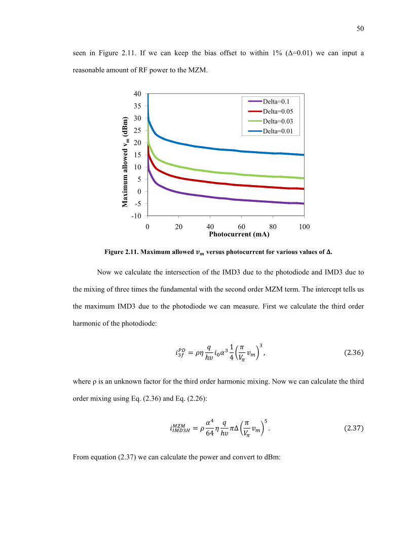
50
seen in Figure 2.11. If we can keep the bias offset to within 1% (Δ=0.01) we can input a
reasonable amount of RF power to the MZM.
Figure 2.11. Maximum allowed versus photocurrent for various values of .
Now we calculate the intersection of the IMD3 due to the photodiode and IMD3 due to
the mixing of three times the fundamental with the second order MZM term. The intercept tells us
the maximum IMD3 due to the photodiode we can measure. First we calculate the third order
harmonic of the photodiode:
where ρ is an unknown factor for the third order harmonic mixing. Now we can calculate the third
order mixing using Eq. (2.36) and Eq. (2.26):
From equation (2.37) we can calculate the power and convert to dBm:
-10
-5
0
5
10
15
20
25
30
35
40
0 20 40 60 80 100
Max
imum
allo
wed
vm
(dB
m)
Photocurrent (mA)
Delta=0.1Delta=0.05Delta=0.03Delta=0.01

51
Using Eq. (2.32) and Eq. (2.38) we can calculate the upper measurement limit of IMD3.
We will plot this equation assuming γ, η, and ρ equal 1. The other variables are defined the same
as above with . The results are plotted in Figure 2.12. We see that the higher order
IMD3 due to the MZM will not cause the measurement setup to be limited.
Figure 2.12. OIP3 limit due to higher order nonlinearities versus output photocurrent
2.4.5 Summary
The three laser two-tone measurement setup has been measured and characterized
analytically and experimentally for the contributing MZM nonlinearities. From our analysis, we
-20
0
20
40
60
80
100
120
140
0 20 40 60 80 100
OIP
MD
H (d
Bm
)
Output Photocurrent (mA)
Delta = 0.1Delta = 0.05Delta = 0.03Delta = 0.01

52
have characterized the nonlinearity contributions from the MZMs, confirming the slopes
measured in Figure 2.8 and demonstrating that the three laser two-tone setup accurately
distinguished unwanted MZM nonlinearities from the photodiode nonlinearity measurement.
Additionally, we looked at the effect of biasing off quadrature has on the maximum input
allowed. Finally, the setup was characterized for the higher limit of OIP3 that can be measured
without the influence of higher order MZM nonlinearities. The higher order nonlinearities show
no significant limitation as long as the bias is kept reasonably close to quadrature.
2.5 Comparing Nonlinearity Measurement Systems
2.5.1 Background and Motivation
Previous work has detailed theoretical mathematical relationships between different
setups [1, 9, 14], however there has been little study to determine when these relationships are
physically true. The mathematical relationships make various assumptions that may not always
hold true in every case for every device. The nonlinearities generated from harmonic and
intermodulation distortions are still largely not understood. Numerous authors have presented
arguments for various causes of nonlinearity in photodiodes [1, 15, 16], but little has been done to
determine the accuracy of the nonlinearity measurements. The aim of this work is to present the
three setups used to measure OIP3, develop the mathematical relationships that may allow
different setups to be interchanged, and then experimentally determine guidelines for when these
relationships can accurately be used.
With the multitude of setups that are used to measure nonlinearities, there has been no
comprehensive study of possible discrepancies between each measurement system and the
conditions under which each system accurately measures photodiode distortion. Considering the

53
two-tone MZM setup, Draa et al. showed that distortions caused by the MZMs could introduce
additional nonlinearities into the measurement, making it inaccurate when using the traditional
setup [1,17]. Ramaswamy et al. proposed using a three-tone MZM setup to eliminate the
contribution of modulator-induced distortions to the measured intermodulation distortions, using
mathematical conversions to relate the measured data to the two-tone setup. The three-tone setup
provided higher OIP3 results under certain situations, leading the authors to conclude that the
three-tone setup is optimal [6]. The authors relied on the mathematical relationship and the higher
OIP3 results to claim that the three-tone MZM setup was more accurate than the two-tone MZM
setup. However the accuracy of the comparison relies on the mathematical relationship between
the two and three-tone setups. If this relationship does not hold up, the results of the two setups
cannot be compared. Additionally, Pan et al. measured devices using both the two-tone and three-
tone MZM setups and showed little measurement differences between the two setups with their
device even at high OIP3 values (~50dBm) [15]. The heterodyning technique has been touted for
its lack of additionally contributed nonlinearities, but is generally considered to be the most
complex of the setups [4].
In all the works mentioned, there is no consensus as to which measurement system
provides the most accurate results, and whether the data from each setup can be equivalently
measured using another. The purpose of this work is to measure a photodiode using the three
widely used setups at various bias voltages and modulation depths. The three-tone MZM and the
one- and two-tone heterodyne systems will be used to measure photodiode distortions in order to
compare nonlinearity data from each setup. The results will determine if and when the theoretical
mathematical relationships can be applied.

54
2.5.2 Measurement Setups
The five-laser heterodyne setup was described in 2.3.1 and can be seen in Figure 2.4. The
five lasers are Lightwave Electronics LWE-125 diode pumped Nd:YAG lasers operating near
1319nm optical wavelength. The tuning range of the LWE-125 laser is about 40GHz, so each set
of heterodyned lasers and the DC laser were each tuned to be 20GHz from each other, far outside
the 3GHz bandwidth of the detector. The single-tone setup is configured by completely turning
off one pair of heterodyned lasers.
The three-tone MZM setup was described in 2.3.4 and can be seen in Figure 2.7. For this
setup, three Lightwave Electronics model-125 diode pumped Nd:YAG lasers operating near
1319nm optical wavelength are modulated by three MZMs and input into optical attenuators. The
first two lasers are combined using a 50/50 coupler, and then to the third with another 50/50
coupler. Finally, an unmodulated Nd:YAG laser is input to an optical attenuator and combined
with the signal using a 50/50 coupler. The output is fed into the DUT, and the RF output is
measured by an ESA. The MZM setup utilizes the same laser wavelengths as the heterodyne
setup to remove measurement differences resulting from optical wavelength dependencies of the
photodiode under test. However, there may still be some discrepancies since the heterodyne lasers
are not modulated, while the lasers modulated by the MZM will set off harmonics, some of which
overlap in the optical domain. For all measurements, 20dB attenuation was required between the
PD DUT and the ESA to ensure that the distortions produced in the ESA were below that of the
PD.
2.5.3 Mathematical Relationships
For the three setups discussed in 2.5.2 the data cannot be readily compared between them
to see if we measure the same OIP3 value. Since one-, two- and three-tone setups the mixing
relationships will be different, we must first find a mathematical relationship to relate the data

55
between the three setups. Once we can establish these relationships, we can use them to compare
data to see if all three setups are consistently measuring OIP3. To determine the mathematical
relationship between the data from each setup, a generalized photodiode nonlinearity, β, will be
designated. For a small signal, the PD nonlinear transfer function can be approximated by a
Taylor series defined by:
The incident optical power in each setup will be defined by a sum of sinusoids:
where for the one-tone heterodyne (which is the setup in Figure 2.4 where the power of
one pair of lasers is turned off), for the two-tone heterodyne and for the three-tone
MZM setup, is the average power, is the modulation index, and is the RF tone
frequency. In the heterodyne setup, the modulation index can be determined by simply
measuring the average power contributions from each of the heterodyned laser pairs and the DC
laser. In the modulator setup, the modulation index can be calculated using the RF input power to
the modulator, optical input power, and modulator transfer function. Substituting (2.41) for
into (2.40) and expanding the resulting equation to the third order (n=3) we obtain:
for the one-tone setup. From (2.42) the coefficients for the fundamental, second order and third
order components can be extracted. Repeating this step for and 3, we have the resulting
distortion for each respectively:

56

57
This small signal approximation comparison holds for any well-behaved single photodiode
nonlinearity, which grows at a higher rate than the fundamental.
When the one, two and three-tone cases are compared with each other, similar distortion
in each case can be compared while keeping the modulation index constant. The second order
relationship, in log scale, using the two-tone setup as the basis, are described by:

58
where represents the second order harmonic distortion for the one-tone setup and
and are the second order intermodulation distortion for the two-tone and three-
tone setups respectively. For the third order distortion, the relationships, in log scale, using the
two-tone setup as the base, are described by:
where and are the third order distortion for the one, two and three-tone
setups respectively. Finally, the relationship between OIP2 and OIP3 for each setup can be
determined. The local OIP2 and OIP3 will be determined by:
where F is the average of all the fundamentals, in dBm, and IMD2 or IMD3 can also be the
harmonic distortion (HD2 or HD3) of the single-tone setup. Using , the relationship
between OIP2, using the two-tone setup as the base, in dBm units of power, is:
Similarly, using the relationship between OIP3 using the two-tone setup as the base, in
dBm units of power, is:
Using these relationships, the data from the one, two and three-tone measurement systems can be
compared.

59
2.5.4 Results and Analysis
A 3GHz-bandwidth photodiode from Applied Electronics (Model: PD3000) was
measured. The measurement was taken around a 100MHz center frequency with 10MHz spacing
for the two and three-tone setups, at 10mA photocurrent. The tones were set to slightly offset
frequencies (i.e. 89.59MHz instead of 90.00MHz) instead of integers to avoid any extraneous
signals present in the environment that might mix and cause distortions at even numbers (i.e.
10MHz, 100MHz). All second and third order intermodulation (and harmonic in the case of the
one-tone setup) products were measured as a function of photodiode bias voltage. Local OIP2 and
OIP3 values were calculated at each bias voltage point using (2.47a) and (2.47b).The data was
plotted at approximately the same input modulation depth across all setups to get the best local
OIP2 and OIP3 comparison between setups.
Figure 2.13 shows the OIP2 versus bias voltage for all second order distortion in the three
setups separated into areas A and B. The plot contains the second order intermodulation
distortions that add (i.e. F1+F2) as well as those that subtract (i.e. |F1-F2|). The one-tone
heterodyne setup provides the second order harmonic (2·F1) at 200MHz. To compare the three
measurement setups, 6dB was subtracted from the OIP21t data such that the OIP2 from all three
measurement systems would align as dictated by (2.48). The three measurement setups are
designated by color, red for the one-tone, blue for the two-tone, and green for the three-tone. The
color scheme for each setup will be maintained throughout the remaining figures. Below 4V bias
(A), the data clearly lines up for low frequency (solid points) and high frequency (open points)
data. Above 4V bias (B), the data at high frequencies for the three-tone setup remain consistent.
There is a large divergence between all three setups from 5-6V. For the low frequency intermods
at high voltages (V > 6V), |F1-F3| and |F2-F3| for the three tone setup merge together along with
|F1-F2| of the two tone, where before 6V |F1-F3| was significantly lower than the distortion closer
to 10MHz (|F1-F2| and |F2-F3|).
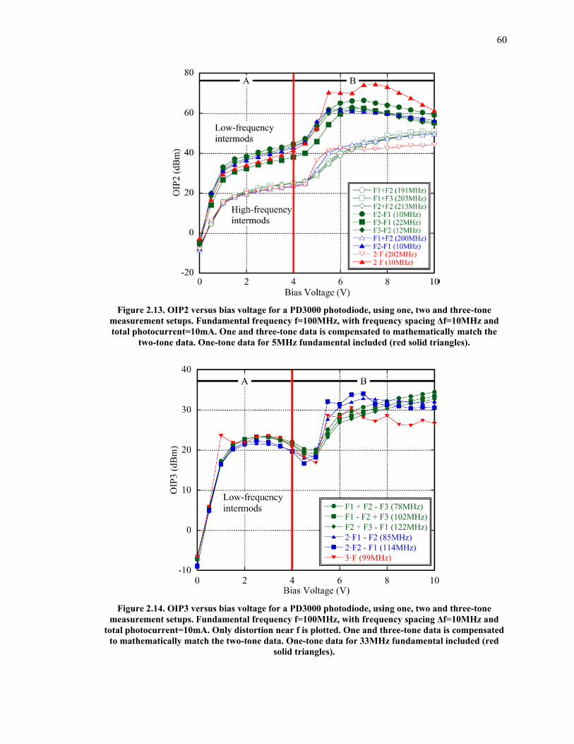
60
Figure 2.13. OIP2 versus bias voltage for a PD3000 photodiode, using one, two and three-tone
measurement setups. Fundamental frequency f=100MHz, with frequency spacing Δf=10MHz and total photocurrent=10mA. One and three-tone data is compensated to mathematically match the
two-tone data. One-tone data for 5MHz fundamental included (red solid triangles).
Figure 2.14. OIP3 versus bias voltage for a PD3000 photodiode, using one, two and three-tone
measurement setups. Fundamental frequency f=100MHz, with frequency spacing Δf=10MHz and total photocurrent=10mA. Only distortion near f is plotted. One and three-tone data is compensated
to mathematically match the two-tone data. One-tone data for 33MHz fundamental included (red solid triangles).

61
In Figure 2.14 OIP3's are plotted versus bias voltage from 0-10V for intermods with
frequencies close to the fundamental frequency. In this instance the MZM setup contributes three
sets of data, F1+F2-F3, F1-F2+F3, and -F1+F2+F3, while the two-tone heterodyne setup
contributes data for 2·F1-F2 and 2·F2-F1. To compare the data sets from each measurement setup,
the two and three-tone data has been shifted as per (2.49), 4.77dB subtracted from OIP31t data
and 3dB is added to OIP33t to normalize to the two-tone setup. The graph is again split into two
areas, A and B. In Figure 2.14, the data matches up well up to 4V in area A (±1dB). In area B (4-
10V), the two-tone setup and three-tone setup no longer overlap. Also, the tones from each
particular setup begin to deviate from each other. For the three-tone setup there is about 1dB
between each case, with the OIP3 decreasing as the frequency of the distortion increases (78MHz,
102MHz, and 122MHz). For the two-tone setup the data crosses back and forth with no clear
pattern. The largest discrepancy between the measurement systems is 8dB (16dB distortion)
which is quite substantial.
Similarly, the OIP3 data for intermods close to the third harmonic frequency are plotted
in Figure 2.15 and again divided into areas A and B at 4V. The three-tone setup provided
F1+F2+F3, the two-tone F1+2·F2 and 2·F1+F2, and the one-tone 3·F1. The data matches well
from 0-4V (area A) as in Figure 2.14; however the three setups begin to diverge above 4V as seen
before in Figures 2.13 and 2.14. After 5V there is a large divergence from any pattern in the data.
The one-tone data in particular is much lower than the other two setups. The OIP3 data is plotted
separately for low and high-frequency cases because the shapes of the curves do not match up at
frequencies that are far apart (similar to the OIP2 case). In the second order case, the low
frequency OIP2s (around 10MHz), are significantly higher than the high frequency OIP2s. The
OIP2 (for the three tone case) that results in double the frequency spacing (|F1-F3|) is slightly
lower than the 10MHz low frequency OIP2s. The behavior has been observed where the lowest

62
frequencies exhibit the highest OIP2, in other diodes. The frequency dependence appears to be
more dominant at low frequencies. Therefore, there is a significant difference in OIP2 between
|F1-F2| and |F1-F3| for the three-tone case, with a separation of 10MHz. With similar separation
at high frequencies there is no difference in OIP2 for F1+F2 and F1+F3. The disparity between
same order distortion as a function of frequency (for both the sum and difference frequencies)
leads to the conclusion there is some frequency dependence in photodiode nonlinearity. As this
behavior has been noticed in some photodiodes but not in others the photodiode itself may be
causing the frequency dependent behavior. Performing the experiments on multiple setups with
more than one diode will give us a better understanding of where these discrepancies result from.
Figure 2.15. OIP3 versus bias voltage for a PD3000 photodiode, using one, two and three-tone
measurement setups. Fundamental frequency f=100MHz, with frequency spacing Δf=10MHz and total photocurrent=10mA. Only distortion near 3·f is plotted. One and three-tone data is
compensated to mathematically match the two-tone data.

63
Figure 2.16. Graphs of the electric field vs. time for one-tone (top), two-tone (middle) and three-tone (bottom) measurements.
Additional data is plotted in Figures 2.13 and 2.14 to analyze this frequency dependence.
The OIP2 from the one-tone setup (red solid triangles) with a 5MHz fundamental resulting in
2·F1 at 10MHz is plotted in Figure 2.13. In area A, the data lines up well with the low frequency
data from the two and three-tone setups that occur near 10MHz, despite originating from a much
lower fundamental frequency. Data is plotted in Figure 2.14 from the one-tone setup (red solid
triangles) with a fundamental of 33MHz, which results in a 3·F1 at 99MHz. The data matches
well for the other nonlinearities that center around 100MHz in area A. The large difference in low
and high frequency second order distortion values can be attributed to the differences in electric
field that the diode sees between the measurement systems. The plots of the electric field for the
one-tone, two-tone and three-tone sinusoidal measurement systems are shown in Figure 2.16,
where the fields are assumed to be parallel. The data in Figure 2.13 and Figure 2.14 from the one-
tone setup at different fundamentals (5MHz and 33MHz) demonstrates that the OIP2 and OIP3
are not necessarily a strong function of the fundamental frequencies. Instead the nonlinearity may
be a function of the time dependent envelopes of the electric field rather than from the higher

64
frequency. Since this behavior has not been observed in all photodiodes more investigation of this
particular diode is necessary to explain the discrepancies that occur at the different frequencies.
The polarizations of all the lasers cannot be simultaneously perpendicular. If the nonlinearities are
perpendicularly polarized for the two-tone system, the resulting field would look like the one-tone
case, possibly causing the distortion to change. The fact that the polarizations of each laser may
be constructively or destructively combining in the device, where the distortion is sensitive to the
electric field, means there are still many factors that we need to quantify in order to accurately
characterize photodiode nonlinearity. Investigating the differences in distortion behavior for the
two-tone case with and without perpendicular polarizations would be useful for future
investigations.
Figure 2.17. Fundamental and selected second and third order distortion power versus modulation depth at 2.5V bias for a PD3000 photodiode. Fundamental frequency f=100MHz, with frequency
spacing Δf=10MHz and total photocurrent=10mA. One and three-tone data is compensated to mathematically match the two-tone data.
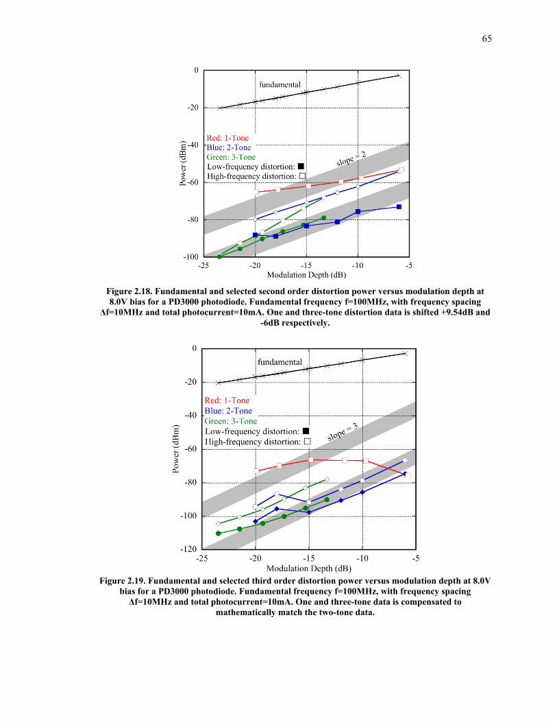
65
Figure 2.18. Fundamental and selected second order distortion power versus modulation depth at 8.0V bias for a PD3000 photodiode. Fundamental frequency f=100MHz, with frequency spacing
Δf=10MHz and total photocurrent=10mA. One and three-tone distortion data is shifted +9.54dB and -6dB respectively.
Figure 2.19. Fundamental and selected third order distortion power versus modulation depth at 8.0V
bias for a PD3000 photodiode. Fundamental frequency f=100MHz, with frequency spacing Δf=10MHz and total photocurrent=10mA. One and three-tone data is compensated to
mathematically match the two-tone data.
66
Now that the diode has been analyzed over bias voltages to determine the setups'
correlation, the relationship of the output RF power versus modulation depth can be discussed. In
Figure 2.17, fundamental, second and third order distortion power is plotted versus modulation
depth at 2.5V bias, corresponding to area A in Figures 2.13-2.15. Again, the distortion data has
been shifted to align with the two-tone setup, as per (2.46). In the plot the second order data
clearly lines up for low and high frequencies at a large range of modulation depths. Additionally
the data are all within 3% deviation of the expected slope value of two. The slopes of the 3rd
order distortion are well behaved (slope of 3 or 60dB/decade) across all measurement setups. All
of the data fall within ±1dB at different modulation depths, indicating that all setups are
measuring the same nonlinearity, and therefore producing the same local OIP. In this case, we
conclude that the measurement setups can be used interchangeably since the mathematical
relationships in (2.48) and (2.49) hold true.
In the case of 8V bias, the data did not show a consistent OIP3 in Figures 2.13-2.15. In
order to understand why this may occur we will look at the output RF power versus modulation
depth for second and third order distortion in Figures 2.18 and 2.19 respectively. In contrast to
Figure 2.17, the slopes of the data do not adhere to the mathematical assumptions made in 2.5.3;
namely, the second order distortion does not have a slope of 2 in relation to the modulation depth
and the third order distortion does not have a slope of 3. It is clear that for high bias voltages the
mathematical description of the diode nonlinearity behavior does not follow from equation (2.40)
in this particular test diode. In the case of 8V the diode may be operating outside our assumptions
or influenced by outside factors (such as the measurement setup) that will no longer allow us to
make the assumptions in 2.5.3 that determined the mathematical relationships between each
setup. One cannot calculate or infer OIP22t or OIP32t from the single tone or 3-tone measurement
systems in this case. The traditional definitions of OIP can no longer be applied to this distortion,
since the 3rd order distortion data in Figure 2.19 does not behave as expected, and cannot be

67
extrapolated. In these cases where the nonlinearities do not grow exponentially, local OIPx
definitions [18] should be utilized.
The data displayed in table 2.1 summarizes the results of Figures 2.17-2.19. The chart
demonstrates that the setups can be accurately compared to within a few dBm if the data versus
modulation depth has a strong slope of two for OIP2 and three for OIP3. In area B the traditional
definition of OIP no longer applies since the distortion does not behave well with the
mathematical relationship. In instances where the distortion does not follow the expected
nonlinear mathematical relationship, the three setups do not give consistent results and therefore
cannot be compared. The inability to compare setups at some voltages could be caused by
different nonlinearities present at different voltages. In the case of low voltages, a single
nonlinearity is probably dominant. As the voltage increases, multiple nonlinearities begin to
manifest, and could interfere in constructive or destructive ways, leading to unconventional
distortion relationships versus modulation depth and thus rendering the setups incomparable, and
the OIP metric itself irrelevant.
Table 2.1. Table showing mean slopes for data in area A (2.5V) and B (8V) of Figures 2.17-2.19.
2.5V data 8.0V data Slope (avg) Slope (avg) 3-Tone IMD2 1.944 2.628
IMD3 3.007 2.301 2-Tone IMD2 1.967 1.571
IMD3 2.962 2.674 1-Tone HD2 1.971 0.832
HD3 2.787 0.531
2.5.5 Polarization Investigation
As mentioned previously the polarization of each beam in any of the setups may play a
part in the measured OIP3 and account for some of the discrepancies between setups. In order to
investigate this issue, we went back to the setup introduced in section 2.3.3, which is the three-

68
laser two-tone MZM setup. In this case we are combining two optical beams that are individually
modulated using a PBC (the reverse of a polarizing beam splitter) to ensure that the modulated
beams are orthogonal. Since in the four-laser three-tone MZM setup it is impossible to have all
three modulated beams perpendicular we will use the two-tone setup as an example. In this case
we measured the photodiode using three lasers all at 1550nm. In the first case we use a 50/50
coupler to combine the two modulated beams and then combine the output with the DC laser
using a 50/50 coupler. In the second case we combine the two modulated beams using two
polarization controllers input into a PBC and then combine the output with the DC laser using a
50/50 copuler. For both tests we use input frequencies of 94.47MHz and 105.59MHz at 10mA
output photocurrent.
Figure 2.20. OIP2 versus bias voltage at 10mA for the case with a 50/50 coupler and PBC.
10
20
30
40
50
60
70
2 3 4 5 6 7 8
OIP
2 (d
Bm
)
Bias Voltage (V)
F1+F2 CouplerF2-F1 CouplerF1+F2 PBCF1-F2 PBC

69
Figure 2.21. OIP3 versus bias voltage at 10mA for the case with a 50/50 coupler and PBC at 2*F2+F1.
In Figure 2.20 we see the OIP2 as a function of bias voltage from 2-8V for both cases
(coupler and PBC), where for most voltages the OIP2 is the same; however from 7-8V the PBC
gives a higher value of OIP2 than the coupler. The difference may indicate some dependence of
the nonlinearity on the polarization (and also premixing that may occur for non-orthogonal
beams). In Figure 2.21 the OIP3 is plotted as a function of bias voltage for the distortion seen at
the frequency 2*F2+F1. In the case of this frequency, the OIP3 is different over the entire range
of voltages, where we measure a higher value of OIP3 with the PBC then with the coupler. We
can also look at the difference between both cases for all third order intermodulation frequencies,
which is shown in Figure 2.22. In Figure 2.22 we see that the OIP3 is relatively the same for the
2*F1-F2 and 2*F1+F2 cases until we reach 7V where we measure a higher value with the PBC.
The OIP3 is significantly higher for the PBC in the case of 2*F2-F1 and 2*F2+F1 over the entire
range of voltages.
12
14
16
18
20
22
24
26
28
2 4 6 8
OIP
3 (d
Bm
)
Bias Voltage (V)
2F2+F1 Coupler2F2+F1 PBC

70
Figure 2.22. Difference in measured OIP3 between PBC and coupler for all intermodulation
frequencies versus bias voltage at 10mA photocurrent.
The data presented in Figures 2.20-2.22 indicate that the polarization plays an integral
role in determining the measurement of nonlinearity. This may account for some of the
discrepancies seen in Figures 2.13-2.15, where the effects from mixing before the device may
cause more nonlinearity at certain biases when the beams are not orthogonal. Kingston theorized
that the mixing that occurs between two plane waves at the surface of a detector is the dot product
of the polarization of the two electric field vectors [19]. Even though the third laser that is
combined using a 50/50 coupler is not modulated, the combination with the previously combined
orthogonal fields, there may be some mixing that occurs. One way to avoid this would be to use a
wavelength that is far enough away from the first two lasers in order to prevent cross modulation
between the two modulated beams. It is important to note that the data presented is for one device
at certain conditions and that the data may vary for devices and other factors such as
-6
-4
-2
0
2
4
6
8
2 4 6 8
Diff
eren
ce in
OIP
3 (d
B)
Bias Votage (V)
2F1-F22F2-F12F1+F22F2+F1

71
photocurrent, bias voltage and frequency. The polarization effect is an important finding that
warrants more investigation in future work.
2.5.6 Summary
Nonlinearity was measured (OIP2 and OIP3) for the PD3000 photodiode using three
setups, a one-tone heterodyne, two-tone heterodyne and three-tone MZM design. The data from
each was compared over a range of 10V bias voltage for a 100MHz center frequency with
10MHz separation between tones. Mathematical relationships were established to compare data
from each setup. Using these relationships we found the data matched well between all setups
from 0-4V where the diode exhibited expected behavior versus modulation depth. From 4-10V
the results diverged for each setup and no longer correlated with the mathematical relationships
we presented in 2.5.3. The slopes versus modulation depth no longer adhered to the mathematical
relationships of two for OIP2 and three for OIP3, invalidating the three setups as a consistent
measurement. Data was also taken using the one-tone setup demonstrating a nonlinearity
correlation resulting from the frequency at which the distortion occurs. Finally the effect of
having non-orthogonally combined beams was investigated using the three-laser two tone setup.
The results so a dependence on bias where in some instances having the modulated beams be
orthogonal resulted in a higher OIP3 and OIP2, indicating possible issues that may prevent the
comparison of different setups.
2.6 Conclusion
In conclusion we have introduced the basics of photodiode nonlinearities and discussed
the various setups used to measured OIP3. The three laser two-tone setup was experimentally and
analytically characterized in depth and shown to be a good solution calibrating out the

72
nonlinearities inherent in the two-laser two tone MZM setup. The setup was experimentally
characterized, where we were able to identify MZM nonlinearities present for a test diode that
were measurable above the noise floor, indicating that we can clearly determine the limit of
accuracy for measuring OIP3, namely when the slope changes from three to two. Additionally we
compared the one-tone heterodyne, two-tone heterodyne and three-tone MZM setups and
analyzed using the mathematical relationships for each using a test diode. The result
demonstrated that the setups can be compared when there is a good slope of three for the OIP3
and slope of two for OIP2. In other cases, where the device nonlinearity is not behaving
conventionally, the data cannot be compared across different setups. From this we understand that
there can be discrepancies between measurement setups which may limit our ability to compare
data across multiple setups. We also looked at the difference in measurement of OIP2 and OIP3
using the three-laser two-tone MZM setup with and without a PBC, In some cases we found using
a PBC resulted in a higher measurement of OIP2 and OIP3. Since this was not true for all
voltages and all frequencies of intermodulation more investigation is needed. For the purpose of
our continued work we will use the three-laser two-tone MZM setup.
2.7 Acknowledgements
Portions of Chapter 2 appear in "Three Laser Two-Tone Setup for Measurement of
Photodiode Intercept Points," published in Optics Express, vol. 16, no. 16, pp. 12108-12113
(2008), Meredith N. Draa, J. Ren, D. C. Scott, W. S. Chang, P. K. L. Yu., the slides in
"Frequency Behaviors of the Third Order Intercept Point for a Waveguide Photodiode Using a
Three Laser Two-Tone Setup," published in IEEE Lasers and Electro-Optics Society (LEOS
2008),Meredith N. Draa, J. Ren, D. C. Scott, W. S. Chang, P. K. L. Yu and "A Comparison of
Photodiode Nonlinearity Measurement Systems," submitted to Journal of Lightwave Technology

73
(2010), Meredith N. Draa, A. S. Hastings, K. J. Williams. Contribution from co-author David C.
Scott is greatly appreciated for the fabrication of the devices measured. Contributions from Jian
Ren for the help with designing the three-laser two-tone setup is greatly appreciated.
Contributions from co-authors Alexander S. Hastings and Dr. Keith J. Williams for contributions
of measurement data as well as insight are greatly appreciated. The author would also like to
acknowledge the insight and guidance provided by Professors Paul Yu and William Chang as
well as funding support through DARPA from both Dr. Steve Pappert and Dr. Ron Esman. The
author of this thesis was the primary author of this work.

74
2.8 References
[1] H. Jiang, D. S. Shin, G. L. Li, T. A. Vang, D. C. Scott, and P. K. L. Yu, “The frequency behavior of the third-order intercept point in a waveguide photodetector,” IEEE Photon. Technol. Lett., vol. 12, pp. 540-542 (2000).
[2] R. B. Welstand, S. A. Pappert, C. K. Sun, J. T. Zhu, Y. Z. Liu, and P. K. L. Yu, “Dual-
Function Electroabsorption Modulator/Detector for Optoelectronic Transceiver Applications,” IEEE Photon Technol. Lett., vol. 8 , pp. 1540-1542 (1996).
[3] P. J. Wuinn and A. H. M. van Roermund, Switched-Capacitor Techniques for High-
Accuracy Filter and ADC Design, Dordrecht, The Netherlands: Springer, 2007, p 140.
[4] D. C. Scott, T. A. Vang, J. Elliott, D. Forbes, J. Lacey, K. Everett, F. Alvarez, R. Johnson, A. Krispin, J. Brock, L. Lembo, H. Jiang, D. S. Shin, J. T. Zhu and P. K. L. Yu, “Measurement of IP3 in p-i-n photodetectors and proposed performance requirements for RF fiber-optic links,” IEEE Photon. Technol. Lett., vol. 12, pp. 422-424 (2000).
[5] R.D. Esman and K. J. Williams “Measurement of Harmonic Distortion in Microwave Photodetectors,” IEEE Photon. Technol. Lett., Vol. 2, no. 7. pp 502 - 504, Jul. 1990.
[6] A. Ramaswamy, N. Nunoya, M. Piels, L. A. Joahansson, L. A. Coldren, J. E. Bowers, A.
S. Hastings, K. J. Williams, and J. Klamkin, "Experimental Analysis of Two Measurement Techniques to Characterize Photodiode Linearity," Int. Topical Meeting on Microwave Photonics (MWP 2009), Valencia, Spain, Oct. 2009.
[7] A. Beling, H. Pan, H. Chen and J. C. Campbell, “Linearity of modified uni-traveling
carrier photodiodes,” J. Lightw. Technol., vol. 26, pp. 2373-2378 (2008). [8] A. Ward III, L. T. Nichols, and R. D. Esman, “RF gain instability in photonic links due to
bias drift in Ti:LiNbO3 Mach-Zehnder modulators,” OFC/IOOC'99. Optical Fiber Communication Conference and the International Conference on Integrated Optics and Optical Fiber Communications, IEEE., vol. 2, pp. 328-30 (1999).
[9] T. Ohno, H. Fukano, Y. Muramoto, T. Ishibashi, T. Yoshimatsu, and Y. Doi, “Measurement of intermodulation distortion in unitravelling-carrier refracting-facet photodiode and a p-i-n refracting-facet photodiode,” IEEE Photon. Technol. Lett., vol. 14, pp. 375-377 (2002).
[10] T. Ozeki and E. H. Hara, “Measurement of nonlinear distortion in photodiodes,” Electon. Lett., vol. 12, pp. 80-81 (1976).
[11] R. R. Hayes and D. L. Persechini, "Nonlinearity of p-i-n photodetectors," IEEE Photon. Technol. Lett., vol. 5, pp. 70-72 (1993).

75
[12] N. G. Kanaglekar, R. E. McIntosh, and W. E. Bryant, “Analysis of two-tone, third-order distortion in cascaded two-ports,” IEEE Trans. Microwave Theory Tech., vol. 36, pp. 701-705 (1988).
[13] G. Brost, “Addressing the requirements for RF photonics,” Proc. SPIE, vol. 5554, pp. 37-45 (2004).
[14] A. Ramaswamy, J. Klamkin, N. Nunoya, L. A. Johansson, L. A. Coldren and J. E. Bowers, “Three-Tone characterization of High-Linearity Waveguide Uni-Traveling-Carrier Photodiodes,” IEEE Lasers and Electro-Optics Society (LEOS 2008), pp. 286-287, 2008.
[15] H. Pan, A. Beling, and J. C. Campbell, “High-Linearity Uni-Traveling-Carrier Photodiodes,” IEEE Photon. Technol. Lett., vol. 21, no. 24, pp. 1855-1857, 2009.
[16] A. S. Hastings, D. A. Tulchinsky, K. J. Williams, “Photodiode Nonlinearities Due to Voltage-Dependent Responsivity,” IEEE Photon. Technol. Lett., vol. 21, no. 21, pp. 1642-1644, 2009.
[17] M. N. Draa, J. Ren, D. C. Scott, W. S. Chang, and P. K. L Yu, “Three laser two-tone setup for measurement of photodiode intercept points,” Opt. Express, vol. 16, no. 16, pp. 12108-12113, 2008.
[18] K. J. Williams, L. T. Nichols, R. D. Esman, “Photodetector Nonlinearity Limitations on a High Dynamic Range 3GHz Fiber Optic Link,” IEEE Journal of Lightwave Technol., vol. 16, no. 2, pp. 192-199, 1998.
[19] R. H. Kingston, Detection of Optical and Infrared Radiation, New York, NY: Pringer-Verlag, 1978, pp. 24-37.

76
Chapter 3 Nonlinearity in PIN Waveguide Photodiodes
3.1 Introduction
Previously in Chapter 2, we investigated the limitations and accuracy of multiple
nonlinearity setups. Our investigations allowed us to better understand the three-laser two-tone
Mach-Zehnder modulator measurement setup and the limitations we face in measuring
intermodulation distortions. Using this information we would like to design and test waveguide
photodiodes for high power and high linearity analog optical links. As discussed in Chapter 1,
there are many design considerations that we must consider for such a device, as there will be a
number of tradeoffs, including power handling capability, responsivity, and bandwidth. We will
continue this discussion with a more detailed look at various design considerations for PIN and
UTC structures for a waveguide photodiode (WGPD) and then present two PIN WGPDs to be
characterized.
The WGPD is a good candidate for the frequency agile links. By using waveguiding
principles to absorb light along the entire length of the photodiode, the PIN WGPD can offer
benefits when compared to a surface normal style photodiodes due to its thin intrinsic region
which results in a fast transit time [1]. Thermal runaway at the front part of the photodiode has
been identified as a failure mechanism for current waveguide style devices [2]. Surface normal
photodiodes have measured very high output third order intercept point (OIP3), 52+dBm, at high
photocurrents at frequencies less than 1GHz [3-5] and slightly lower values at high frequencies
by using a high Carbon doped absorber [4]. Previous WGPDs have demonstrated a reduction in
optical overlap factor which resulted in OIP3 measurements up to 40.9dBm at 80.6mA at 1GHz

77
using a uni-traveling carrier (UTC) style PD [6]. Additionally, Jasmin et al. adjusted the active
region in the intrinsic region to control confinement factor and increase efficiency [7]. The
significance of this work is to look at the interplay between bandwidth limitations, power
handling capability and OIP3 performance for PIN style waveguide photodiodes. We intend to
show the benefits of decreasing the optical overlap factor for a PIN photodiode by reducing the
absorption layer thickness and lengthening the device. We will look at linearity and power
handling capability, which will allow us to continue design of future devices that need to be high
power and high linearity. Additionally, we will use a basic circuit model to look at one of the
devices and use it to establish approximately what parameter values we will need in order to
achieve better nonlinearity in future devices.
3.2 Background
3.2.1 Surface Normal PIN Photodiodes
A PIN photodiode is made of a p-type layer and n-type layer with an intrinsic or i-layer
between. Typically the i-layer is an undoped layer where the absorption occurs [8]. For links
operating around 1.55 µm wavelengths, indium-gallium-arsenide (InGaAs) is a widely used
material since it has a bandgap around 1.6 µm and its direct bandgap provides a large absorption
coefficient. InGaAs will be the material used throughout this work for optical absorption in all
photodiodes discussed. Another material that has similar absorption properties to InGaAs is
germanium (Ge), however due to its high dark current, InGaAs is generally preferred [8]. Recent
advances in passivation techniques have provided dark current as low at 4.1×10⁻⁵ A/cm2 with an
external quantum efficiency of 32% for Ge devices [9].
The design of the PIN photodiode provides an ability to absorb photons, thus creating an
electron and hole pair, and sweep the carriers out to their respective ends and collected at an

78
external circuit with the help of an applied electric field. Figure 3.1a shows the bandgap structure
of a PIN photodiode, while Figure 3.1b shows the resulting electric field from reverse biasing the
diode. Assuming a surface normal structure, the quantum efficiency ( is defined as the
number of photo-generated electrons divided by the number of incident photons [8]. The of
such a photodiode, neglecting scattering and free-carrier absorption, is [10]:
where is the diffusion length of holes, d is the thickness of the intrinsic region and α is the
absorption coefficient. If we look at the carrier transit time for such a device, where the electric
field is applied across the intrinsic layer [11]:
where is the electron mobility and V is the applied bias (except in cases of high power where
not all of the voltage will be across the intrinsic layer), we see that as d increases so does , but
in order to increase efficiency d must be increased for a surface normal structure. In the case
where the velocity is saturated, the transit time will not be voltage dependent as in (3.2).
Neglecting this case, the typical PIN photodiode which is surface normal illuminated, shown in
Figure 3.2, can be limited in bandwidth when attempting to maintain a high efficiency. In the
cases where the surface normal is not RC limited, but transit time limited, the solution for this is
provided by using a waveguide style photodiode, as described in section 3.2.2.

79
(a)
(b)
Figure 3.1. (a) PIN photodiode band diagram and (b) electric field of reverse biased PIN photodiode.
Figure 3.2. Surface normal photodiode.
Ni
P
Band Gap, Eg
Depletion Region
Conduction Band
Valence Band
Optical Input

80
For a surface normal PIN photodiode there will be a tradeoff between capacitance (area)
and high power handling as well. If we define the device capacitance as:
where d is the thickness of the intrinsic region and A is the area of the device, we see that a
smaller area and thicker intrinsic layer will lead to a lower capacitance. As we decrease the area,
the power handling capability will decrease as the thermal resistance is related by [12]:
Equation (3.4) tells us that the thermal resistance decreases as the device area increases and the
intrinsic thickness decreases (assuming the heat is located primarily in the intrinsic layer).
Equations (3.1) through (3.4) present design tradeoffs for a surface normal PIN photodiode.
Overall, PIN photodiodes provide broad bandwidth, high linearity and temperature stability [13],
which are qualities all necessary for high SFDR links which require high bandwidth. Next we will
discuss the PIN photodiode in detail for a WG structure including the tradeoffs we will consider.
3.2.2 Waveguide PIN Photodiodes
A number of performance improvements can be obtained by using a waveguide style
photodiode, seen in Figure 3.3. The light is input transversely to the active layer, instead of
normal to the junction plane. The photocurrent density is given by:
where is the optical power, is the electronic charge, is the photon energy, is the optical
confinement factor, is the absorption coefficient and is the input coupling coefficient. The
optical confinement factor is the ratio of the optical energy of the mode in the active medium to
the total optical energy of the mode in the cavity [14].The confinement factor represents the
amount of light that is present in the absorbing layers along the waveguide, which will determine

81
the absorption profile and current density along the device. From equation (3.5) we can integrate
over the device length to find the quantum efficiency of a WGPD:
In this case, d can be chosen so that an appropriately high transit time can be achieved, while L
can be increased so that 100% quantum efficiency can be achieved. Altering the absorption layers
thickness, d, will not only reduce the transit time but will also reduce Γ as there will be less
overlap of the waveguide field evanescent tail and therefore less absorption. The responsivity of a
WGPD is generally smaller than a surface normal PD due to the modal mismatch between the
waveguide and the single mode fiber [15]. However, since the absorption is now traverse to the
transit of carriers, the WGPD has a larger bandwidth-efficiency performance than SN
photodiodes. Additionally, even if L is relatively large, a narrow waveguide and detector can be
used in order to keep capacitance small and bandwidth high [10]. The transit time limit is
inversely proportional to the intrinsic region thickness, but the RC limit is proportional to L,
indicating a tradeoff between the two.
Figure 3.3. Waveguide photodiode where the light is coupled to a mode profile determined by the
waveguiding layers of the structure.

82
3.2.3 PIN versus UTC Waveguide Photodiodes
As discussed in Chapter 1, the uni-traveling carrier photodiode has the benefit of a large
absorption area and high transit speed from the electrons being the primary carriers, while
incorporating a thin intrinsic layer for surface normal photodiodes. In the case of a WGPD, a
UTC structure can provide faster transit as the electrons will be the primary carrier. However,
since the WGPD is side illuminated, a thick absorbing layer will result in a high current density at
the front facet. The quantum efficiency benefit achieved with a surface normal design is not as
important for a WGPD when considering a UTC layer structure. UTC WGPDs have shown high
linearity with an OIP3 of 42dBm at 23mA [16]. Another benefit of using a UTC structure for a
WGPD is that InGaAs has a very poor thermal conductivity (0.05 W/cm/K) which causes device
heating in the intrinsic region for a PIN PD. Since thermal considerations are more stringent for a
WGPD due to the uneven current density distribution, improving the thermal properties of the
intrinsic region is an important design consideration. In order to reduce front end current density,
the absorber can be thinned and the device length increased so as to reduce the overall optical
overlap factor. In the rest of the chapter, a study of two devices allows us to look at the tradeoffs
for controlling Γ while maintaining the same responsivity.
3.3 Device Structures and Modeling
3.3.1 Device Structures
Two PIN waveguide (WG) photodiodes will be discussed in this chapter. The devices
were designed with high linearity in consideration, as well as high power. The original device, A,
is designed for a 20GHz link. The second structure (designated device B) is a modification of
device A, where we intend to see if there are benefits to reducing the overlap factor, but
maintaining efficiency (by increasing device length). Additionally, we would like to look at the

83
tradeoff between power and bandwidth (where the increased length provides more device area but
negatively affects the capacitance). The epitaxial structures can be seen in Table 3.1 where the
variable X corresponds to the absorber thickness indicated in Table 3.2. There is a 0.01μm thick
layer of p-InGaAs, followed by the p-InP barrier layers. Next there are three layers of intrinsic
InGaAsP that are unintentionally doped (UID) and 0.007μm which provide bandgap smoothing.
The purpose of the bandgap smoothing is to reduce carrier pile-up at the p-i and i-n interfaces
where bandgap discontinuities occur. The discontinuities contribute to charge screening at high
power as carriers are not able to leave the intrinsic region and will alter the electric field near the
interfaces, causing saturation and nonlinearity. The absorber thickness is determined in Table 3.2.
Next there are three more layers of UID InGaAsP to smooth out the bandgap and provide the
remaining intrinsic region. Finally there is 0.59μm of n-type InGaAsP. The waveguiding layers
are indicated in orange, where the lighter orange layer is also part of the intrinsic region. Both
device mesas are 5μm wide with the length depending on the design. The devices are designed to
have 20GHz and 10GHz bandwidth for device A and B respectively. The two factors that are
modified are the absorption layer thickness, which is reduced, and the length, which is increased,
from device A to device B. The result of the reduced absorption layer thickness is a smaller
optical overlap factor for device B. Both devices are anti-reflective coated with Al2O3.

84
Table 3.1. PIN waveguide layer structure with bandgap wavelengths in parenthesis.
For Device B, the absorber is made thinner, but the intrinsic layer thickness is maintained
the same to examine the effects of reducing the front facet heating and absorption along the
length of the device. Additionally, the longer device is necessary to maintain similar responsivity
for each device since the overlap factor (Γ) is significantly reduced in device B. Table 3.2 shows
the design parameters for each device. The layer structures are shown in Table 3.2 where X
corresponds to the absorber layer thickness detailed in Table 3.1. The length of device B is almost
twice as long as device A because of the capacitance requirements for the bandwidth design and
to maintain responsivity.
Table 3.2. Device design parameters.
Device A Device B
Bandwidth (GHz) 20 10
Width (μm) 5 5
Length (μm) 55 100
Absorber (‘X’) (μm) 0.035 0.016
Γ 0.0367 0.0094
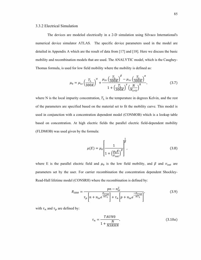
85
3.3.2 Electrical Simulation
The devices are modeled electrically in a 2-D simulation using Silvaco International's
numerical device simulator ATLAS. The specific device parameters used in the model are
detailed in Appendix A which are the result of data from [17] and [18]. Here we discuss the basic
mobility and recombination models that are used. The ANALYTIC model, which is the Caughey-
Thomas formula, is used for low field mobility where the mobility is defined as:
where N is the local impurity concentration, is the temperature in degrees Kelvin, and the rest
of the parameters are specified based on the material set to fit the mobility curve. This model is
used in conjunction with a concentration dependent model (CONMOB) which is a lookup table
based on concentration. At high electric fields the parallel electric field-dependent mobility
(FLDMOB) was used given by the formula:
where E is the parallel electric field and is the low field mobility, and and are
parameters set by the user. For carrier recombination the concentration dependent Shockley-
Read-Hall lifetime model (CONSRH) where the recombination is defined by:
with and are defined by:

86
and N is the local impurity concentration. The rest of the parameters can be user specified based
on the material. Lastly the FERMI model was specified in order to use Fermi Dirac statistics, with
reduced carrier concentrations in heavily doped regions.
We simulated the DC responsivity curve which can be seen in Figure 3.4. The light is
top down illumination. Since both devices are waveguide style, the output is scaled to 3D using
the device geometry and the optical overlap factor. The simulation looks at a 2D structure that is
1µm wide. The current density is multiplied by the width (5µm) and length (device A: 55µm and
device B: 100µm). The optical overlap factor is determined by simulation using BeamProp and
then is used to scale the overall photocurrent as a function of device length, since the simulation
assumes top down illumination, which gives a uniform absorption. The simulation does not take
into account the thermal heating that occurs in the device and has not been calibrated with
measured data. The results indicate a higher expected 1dB DC saturation for device B. The
electric field is reduced by charge-screening at high powers as more carriers are in the intrinsic
region. The compression of the output photocurrent at high optical power can be attributed to the
carrier buildup in the intrinsic region, which results in increased recombination and compression
of the photocurrent. The increase in carriers in the intrinsic region (as input optical power is
increased) results in a redistribution of electric field which can be seen in Figures 3.5 and 3.6 for
device A and B respectively. The devices were modeled without a load, so that the electric field
redistribution occurs from the highest output photocurrent level shown in each plot there is some
negative electric field seen that is also due to the simulation setup which lacks a 50Ω load.
Although the behavior is similar, the collapse of the electric field occurs at very different
photocurrent levels that correspond to the curves in Figure 3.4. Later results will demonstrate the
beneficial behavior of device B in terms of linearity.

87
Figure 3.4. Simulation of DC responsivity for device A and B.
Figure 3.5. Electric field at various levels of photocurrent for device A without a load.
0
50
100
150
200
250
300
350
400
0 200 400 600 800 1000Input Optical Power (mW)
Ou
tpu
t P
ho
tocu
rren
t (m
A)
Device ADevice B
-100
0
100
200
300
400
500
0.5 1 1.5 2
Ele
ctri
c Fi
eld
(kV
/cm
)
Distance Along Device (um)
6mA61mA81mA108mA135mA180mA

88
Figure 3.6. Electric field at various levels of photocurrent for device B without a load.
3.3.3 Thermal Simulation
We simulated the devices for thermal heating using COMSOL. The devices are setup in
3D based on the geometry and the bulk conductivities for each layer. In the simulation, the power
density is defined along the length of the device according to:
where is the input optical power, is the width of the mesa, is the height of the intrinsic
region, is the electronic charge, is Planck’s constant, ν is the frequency, is the bias voltage,
is the optical overlap factor, α is the absorption coefficient and η is the input optical coupling
efficiency. The device is simulated over a range of input power and the maximum temperature in
the device is recorded. The output photocurrent can be found by integrating (3.11) over the length
of the device, multiplying by the device width and intrinsic thickness and dividing by the bias
voltage:
-100
0
100
200
300
400
500
0.5 1 1.5 2
Ele
ctri
c Fi
eld
(kV
/cm
)
Distance Along Device (um)
5mA57mA113mA170mA227mA322mA

89
where L is the length of the device. Using data from device A the output photocurrent is scaled to
approximate that the device fails at 600K. From this, device B can be compared in measurement
to assess whether the model predicts the failure point. The results of the simulation can be seen in
Figure 3.7. The simulation predicts that device B will fail at slightly twice the amount of
photocurrent of device A, where we use 600K as our temperature that we assume catastrophic
failure. In Figure 3.8, the heat distribution can be seen for device A at 100mW input optical
power and -4V bias. The maximum temperature reached is 477K. The highest temperatures are
seen in the intrinsic layers which is expected since this is where the heat is generated due to the
applied bias voltage.
Figure 3.7. Simulation of heating in device A and B at -4V bias.
300
350
400
450
500
550
600
650
0 20 40 60 80Output Photocurrent (mA)
Max
imum
Dev
ice
Tem
pera
ture
(K)
Device ADevice B

90
Figure 3.8. Device A heating at 100mW input power and -4V bias.
3.4 Experimental Results and Discussion
3.4.1 Bandwidth Measurement
The devices were measured for bandwidth using an Agilent 86030A Lightwave Analyzer.
The bandwidth measurements were made up to 50GHz at -4V bias and 1mW input optical power
and can be seen in Figure 3.9 and Figure 3.10 for device A and B respectively. The graphs show
measurements for many of the same devices to demonstrate the consistency of the bandwidth.
The bandwidths are 20GHz and 10GHz for device A and B at low input optical power.
Additionally, the device photocurrent failure point was measured at -4V bias with a result of
32mA and 49.3mA for device A and B. Device B exhibits almost two times the current capability
of device A at -4V bias due to the reduction in optical overlap and the increased length of the
device. Calculating the transit time bandwidth using we find for both devices the

91
approximate transit time bandwidth is 139GHz which is much larger than the RC limited
bandwidth seen in Figure 3.9. The rate of roll-off for Figure 3.10 is higher due to the fact that
device B has a higher capacitance than device A.
Figure 3.9. Normalized frequency response of device A up to 50GHz.
Figure 3.10. Normalized frequency response of device B up to 50GHz.
-15
-10
-5
0
0 10 20 30 40 50
Frequency (GHz)
Mag
nitu
de (d
B)
-15
-10
-5
0
0 10 20 30 40 50Frequency (GHz)
Mag
nitu
de (d
B)

92
3.4.2 DC Saturation
The devices were measured for DC saturation at -2V bias with a responsivity of .5A/W
and can be seen in Figure 3.11 along with the simulated DC saturation curves performed in
Silvaco using surface normal illumination. The maximum recorded responsivity of each device is
.75A/W and .74A/W for device A and B respectively. The saturation point was determined by
recording output DC photocurrent versus input DC optical power and finding a linear line of best
fit at low input power to determine the approximate photocurrent where DC saturation begins.
Device A begins to saturate at about 75mA while device B did not saturate, but exhibited thermal
runaway and failed at 160mA. The simulation was scaled according to device geometry
parameters as detailed above and then calibrated to the results. The simulation does not predict
saturation as in the 4V bias case for device B seen in Figure 3.4. In Silvaco, the electric field is
observed to collapse which should induce saturation. Instead we observe a large increase in
electron current density occurs in the p-region overtaking the hole current density, which leads to
recombination near the intrinsic region to p-region interface, where the recombination will release
heat. We believe the recombination reduces the carrier densities and accounts for the observed
induced electric field in the intrinsic region that is seen in the simulation. From this observation
we believe the field across the intrinsic region increases the carrier transport to their saturation
velocities causing the runaway current observed in the measurement. As discussed earlier, the
simulation does not contain a load, which will alter the electric fields in the simulation.

93
Figure 3.11. DC saturation measurement and simulation (black) for device A (blue) and device B
(red) at -2V bias.
3.4.3 Nonlinearity Measurement
The device OIP3 was measured using the three laser two-tone setup in 2.3.3. Two
distributed-feedback lasers were externally modulated and amplified with an erbium doped fiber
amplifier (EDFA). The EDFA is held at constant power and the output at each is attenuated using
a variable optical attenuator (VOA) and then combined with a 50/50 coupler. A third un-
modulated distributed feedback laser is amplified with an EDFA and also controlled by a VOA.
The two branches are combined with a wavelength division multiplexer (WDM) and input into
the device. The measurements were made as discussed in 2.3.3 where the slope is three to ensure
third order distortion at the given frequency is due to the detector alone.
0
50
100
150
200
0 50 100 150 200 250 300Input Optical Power (mW)
Out
put P
hoto
curr
ent (
mA
)
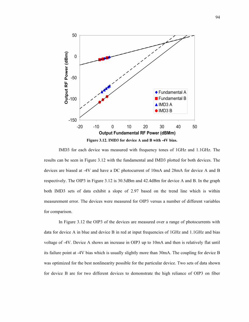
94
Figure 3.12. IMD3 for device A and B with -4V bias.
IMD3 for each device was measured with frequency tones of 1GHz and 1.1GHz. The
results can be seen in Figure 3.12 with the fundamental and IMD3 plotted for both devices. The
devices are biased at -4V and have a DC photocurrent of 10mA and 28mA for device A and B
respectively. The OIP3 in Figure 3.12 is 30.5dBm and 42.4dBm for device A and B. In the graph
both IMD3 sets of data exhibit a slope of 2.97 based on the trend line which is within
measurement error. The devices were measured for OIP3 versus a number of different variables
for comparison.
In Figure 3.12 the OIP3 of the devices are measured over a range of photocurrents with
data for device A in blue and device B in red at input frequencies of 1GHz and 1.1GHz and bias
voltage of -4V. Device A shows an increase in OIP3 up to 10mA and then is relatively flat until
its failure point at -4V bias which is usually slightly more than 30mA. The coupling for device B
was optimized for the best nonlinearity possible for the particular device. Two sets of data shown
for device B are for two different devices to demonstrate the high reliance of OIP3 on fiber
-150
-100
-50
0
50
-20 -10 0 10 20 30 40 50Output Fundamental RF Power (dBMm)
Ou
tpu
t R
F P
ow
er (
dB
m)
Fundamental AFundamental BIMD3 AIMD3 B

95
coupling. The circle data shows a significant increase in OIP3 over photocurrent and overall is
between 5 to 10dBm higher than device A with a peak occurring at 28mA. The triangle data
shows the same increase in OIP3 as photocurrent increases but a flatter response from 20mA to
30mA. During measurements a specific fiber position could be tweaked to see approximately a
10dBm reduction in IMD3 with little effect on the fundamental thereby significantly increasing
OIP3. In device A, the fiber positioning was not observed to have a significant effect on OIP3
while maintaining a consistent responsivity. Because of the difference in device structures, there
may be a difference in the excitation and propagation of the optical modes which would lead to
different thermal distributions and possibly generated distortions that could make OIP3 of device
B more sensitive to the fiber position.
Figure 3.13. OIP3 for device A and B with -4V bias at 1GHz.
0
15
30
45
0 10 20 30 40 50Output Photocurrent (mA)
OIP
3 (d
Bm
)
Device B
Device A

96
Figure 3.14. OIP3 for device A and B at 15mA and 20mA at 1GHz.
Both devices were measured over a range of bias voltages which can be seen in Figure
3.14. The purpose of this measurement was to determine the optimal bias point of the device
when considering linearity and thermal heating tradeoffs. At a higher bias the device may have
better linearity, but will dissipate more power. For device A, the measurements were taken at
15mA photocurrent from -2V to -6V. The device failed at -6V and at about 90mW of power. For
device B, the measurements were taken at 20mA from -2V to -9.5V, where the device failed at
about 190mW of power, which is almost double that of device A. In Figure 3.14, the OIP3 shows
an increase from -2V to -4V and then a leveling off for both devices, with device B about 8dBm
higher for OIP3. Device B however shows an increase in OIP3 from -7V to -9.5V with a peak of
40.5dBm for OIP3 at -9.5V. Both devices were designed to operate at -4V, in order to maximize
linearity by maintaining a particular electric field across the device that is below the breakdown
voltage but greater than the point at which carrier velocities are no longer constant. From the
results is the desired bias operation is confirmed with the leveling off of OIP3 at voltages higher
than -4V.
0
15
30
45
0 2 4 6 8 10Bias Voltage (V)
OIP
3 (d
Bm
)
Device A Ipd=15mADevice B Ipd=20mA

97
Figure 3.15. OIP3 for device A at 10mA and B at 25mA and -4V bias versus frequency.
Next OIP3 is measured over a range of frequencies. The results can be seen in Figure
3.15 for device A and B. Device A is measured from 1-18GHz at 10mA output photocurrent and -
4V bias with an initial OIP3 of 32.7. The device exhibits a flat response up until about 16GHz
where OIP3 begins to roll off, which interestingly looks similar to the responsivity roll off
although the two may not necessarily have any correlation. The OIP3 roll off may be influenced
by both thermal and transit time effect. Device B is measured from 1-10GHz at 25mA output
photocurrent and -4V bias with an initial value of 34.6dBm. The device has a flat response up
until 8GHz where there is a slight roll off.
In summary, device B exhibits better linearity at photocurrents higher than 5mA. In
device B, the optical confinement factor is lower which does two things. First the absorption
profile is more spread out, which reduces the thermal heating at the front facet. Second the
current density is more uniform along the device. We believe the more uniform current
distribution reduces the charge screening effects as well as thermal heating, both of which can
cause more nonlinearity. Device B has an increase in OIP3 at higher bias voltage which is due the

98
higher electric field being able to sustain high current densities before charge screening and
saturation occur. From our experimental investigation we find the tradeoff of bandwidth has
resulted in a significant improvement in DC saturation, power handling capability and linearity.
The reduction of current density and a uniform distribution is critical for future designs that we
would like to be both high power and high linearity.
3.5 Nonlinearity Modeling by Equivalent Circuit Analysis
Various models have been presented for analyzing photodetector nonlinearities [19-20],
and a model for high bias voltage demonstrated a constant IP3 for low frequency and a
dependence ~f -3 at high frequency [21]. Jiang’s model uses an equivalent circuit with
impedances calculated from the photodiode’s microwave reflection coefficient (S11)
measurement. We use this model to extract the device parameters at various output
photocurrents. The data from device A presented in Figure 3.15 will be analytically modeled. The
circuit model diagram is shown in Figure 3.16. The current, i, is given by:
where R1 is the optical power dependent differential resistance, C1 is the optical power dependent
differential capacitance, C0 and R0 are the junction capacitance and junction resistance at a given
DC photocurrent, Rs is the series resistance, RL is the load resistance, and Cp is the parasitic
capacitance. Assuming two RF current sources we can write:
Substituting (3.14) into (3.14) and using the harmonic balance method we can solve for the IMD3
coefficients as well as the fundamental. For IMD3 we have:

99
The full equations and analysis for V52a and V52b can be found in Appendix B.
Figure 3.16. Photodiode circuit model diagram.
OIP3 is modeled in green in Figures 3.17 and 3.18 with the measured values in red. The
values for each parameter are detailed in Table 3.3. There is good agreement with the circuit
model up to ~16GHz but after that the data drops off much quicker. In Figure 3.17a, the effects of
increasing C0 were investigated. In this case we find that as the initial capacitance increases the
OIP3 at higher frequencies decreases, which is as expected. Similarly C1 was increased and we
find that this has a positive effect on OIP3 at high frequencies. This is due to the fact that if the
differential capacitance is increasing in value, the overall capacitance is reducing as current
increases. Since a large capacitance will result in a faster roll-off of OIP3, the high differential
capacitance results in a lower overall capacitance at high photocurrent, causing the behavior seen
in Figure 3.17b. Additionally, we looked at the effects of increasing R0 which caused OIP3 to
increase at low frequencies. This is due to the fact that a high shunt resistance equates to high
OIP3 at low frequencies. Lastly, R1 was increased and we see that this negatively affects OIP3
almost uniformly versus frequency, which indicates that a low differential resistance is beneficial
for OIP3.

100
(a)
(b)
Figure 3.17. Effect on OIP3 for increasing (a) C0(fF) with values 200, 400, 600, 800, and 1000 and (b)
C1(fF/mA) with values of 6, 8, 10, 12, and 14.

101
(a)
(b)
Figure 3.18. Effect on OIP3 for increasing (a) R0(kΩ) with values of 125, 145, 165, 185, and 205 and (b) R1(kΩ/mA) with values of 33, 35, 37, 39, and 41.

102
Table 3.3. Extracted values for circuit parameters that match OIP3 data from device A.
Parameter Value Parameter Value Rs (Ω) 25 Cp (fF) .0001 R0 (kΩ) 125 C0 (fF) 200 R1 (kΩ/mA) 33 C1 (fF/mA) 6
From the analytical model, we find that we would like a very high junction resistance on
the order of 200kΩ and above where this resistance is maintained as a function of photocurrent
(i.e. low differential junction resistance). In order to achieve high OIP3 over bandwidth of the
device we would like to keep the junction capacitance low, ideally on the order of 10's of fF,
while having the negative differential capacitance around 8fF/mA if possible. Previous work has
shown that highly doping the p-region next to the i-region using carbon as the dopant made the
junction profile less gradual which has shown to lower junction capacitance [4]. Using this
information and the parameters from the model we can incorporate this into future devices. We
would like to note that we have not presented a nonlinearity model, but rather used the small
signal equivalent circuit to extract circuit parameters.
3.6 Conclusion
Two WGPD devices were fabricated and characterized demonstrating the effects of
reducing the optical overlap factor and increasing thermal capacity through lengthening the
device, with the tradeoff of bandwidth. The devices were characterized first through two
simulation programs for output DC saturation and thermally for device maximum photocurrent.
The 1dB DC saturation points were measured as 80mA and >150mA for device A and B. Device
B showed a high dependence of OIP3 on fiber positioning due to the decreased absorber
thickness. A significant enhancement of OIP3 and power capability is observed for device B with

103
a record high maximum OIP3 of 42.4dBm at 28mA and 1GHz frequency for a PIN waveguide
photodiode. We find that the reduction of the optical overlap factor provides significant linearity
improvement, (>10dB at 30mA) and almost double the DC saturation point, with a reduction in
bandwidth by half. The relationships between bandwidth (capacitance), thermal resistance and
responsivity were outlined section 3.2. Additionally, not only did the device thermal performance
improve but the linearity improved as well. In our future design we will seek to develop a device
that aims to more uniformly distribute the absorption throughout the device, to gain both thermal
and linearity improvements; however we would like to find a solution to avoid the reduction in
bandwidth capability that we saw from device B. Chapter 4 will discuss a new design that uses
the design considerations investigated in this chapter, while also incorporating a UTC style
structure with a WGPD.
3.7 Acknowledgments
Portions of Chapter 3 appear in "Behaviors of the Third Order Intercept Point for PIN
Waveguide Photodiodes," published in Optics Express, vol. 17, no. 16, pp. 14389-14394 (2009),
Meredith N. Draa, J. Bloch, D. C. Scott, N. Chen, S. B. Chen, W. S. Chang, and P. K. L. Yu and
"Frequency behaviors of the third order intercept point for a waveguide photodiode using three
laser two-tone setup," published in IEEE Lasers and Electro-Optics Society (LEOS 2008),
Meredith N. Draa, J. Ren, D. C. Scott, W. S. Chang, and P. K. L. Yu. Contribution from co-
author Dr. David C. Scott is greatly appreciated for the fabrication of the devices and RF response
measurements. The author would also like to thank Jeff Bloch for his contributions to the device
designs. The author would also like to acknowledge the insight and guidance provided by
Professors Paul Yu and William Chang as well as funding support through DARPA from both

104
Dr. Steve Pappert and Dr. Ron Esman. The author of this thesis was the primary author of this
work.

105
3.8 References
[1] D. C. Scott, T. A. Vang, J. Elliott, D. Forbes, J. Lacey, K. Everett, F. Alvarez, R. Johnson, A. Krispin, J. Brock, L. Lembo, H. Jiang, D. S. Shin, J. T. Zhu and P. K. L. Yu, “Measurement of IP3 in p-i-n photodetectors and proposed performance requirements for RF fiber-optic links,” IEEE Photon. Technol. Lett., vol. 12, pp. 422-424 (2000)
[2] H. Jiang and P. K. L. Yu, “Waveguide integrated photodiode for analog fiber-
optic links,” IEEE Trans. Micro. Theory and Tech., vol. 48, pp. 2604-2610 (2000).
[3] A. Beling, H. Pan, H. Chen and J. C. Campbell, “Linearity of modified uni-traveling carrier photodiodes,” J. Lightw. Technol., vol. 26, pp. 2373-2378 (2008).
[4] H. Pan, Z. Li, A. Beling, and J. C. Campbell, "Measurement and modeling of high-linearity modified uni-traveling carrier photodiode with highly-doped absorber," Opt. Express, vol. 17, pp. 20221-20226 (2009).
[5] H. Pan, A. Beling, and J. C. Campbell, "High-Linearity Uni-Traveling-Carrier Photodiodes," IEEE Photon. Technol. Lett., vol. 21, pp. 1855-1857 (2009).
[6] J. Klamkin, A. Ramaswamy, N. Nunoya, L. A. Johansson, J. E. Bowers, S. P. DenBaars and L. A. Coldren, “Uni-traveling-carrier waveguide photodiodes with >40dBm OIP3 for up to 80mA of photocurrent,” IEEE J. Quant. Tech., vol. 44, pp. 354-359 (2008).
[7] S. Jasmin. N. Vodjdani, J. Renaud, and A. Enard, "Diluted- and distributed-absorption microwave photodiodes for high efficiency and high power," IEEE Trans. Microwave Theory and Tech., vol. 45, pp. 1337-1341 (1997).
[8] C. H. Cox, III, Analog Optical Links New York, NY: Cambridge, 2004, pp. 49-51.
[9] J. Osmond, G. Isella, D. Charastina, R. Kaufmann, M. Acciarri, and H. von Kanel, "Ultralow dark current Ge/Si (100) photodiodes with low thermal budget," Appl. Phys. Lett., vol. 94, pp. 201106-1-3 (2009).
[10] R. G. Hunsperger, Integrated Optics: Theory and Technology New York, NY: Springer, 2009, pp 347-349.
[11] M. Shur, Physics of Semiconductor Devices Englewood Cliffs, NJ: Prentice-Hall, 1990, pp 502.
[12] R. Remsburg, Advanced Thermal Design of Electronic Equipment New York, NY: Chapman & Hall, 1998, pp. 499.
[13] D. Derickson, Fiber Optic Test and Measurement Upper Saddle River, NJ: Prentice Hall, 1998, pp. 249.

106
[14] W. S. C. Chang, Principles of Lasers and Optics New York, NY: Cambridge University
Press, 2005, pp. 222.
[15] W. S. Chang, RF Photonic Technology in Optical Fiber Links, New York, NY: Cambridge, 2002, pp. 248-250.
[16] J. Klamkin, Y.-C. Chang, A. Ramaswamy, L. A. Johansson, J. E. Bowers, S. P. DenBaars, and L. A. Coldren, "Output Saturation and Linearity of Waveguide Unitraveling-Carrier Photodiodes," J. Quantum Electon., vol. 44, no. 4, pp. 354-359 (2008).
[17] Srivastava, Shivani, “Simulation Study of InP-Based Uni-Traveling Carrier Photodiode” Masters Thesis, University of Cincinnati (2003).
[18] Siklitsky, Vadim, "Electronic Archive: New Semiconductor Materials. Characteristics
and Properties," Ioffe Physico-Technical Institute http://www.ioffe.rssi.ru/SVA/NSM/.
[19] K. J.Williams, R. D. Esman, and M. Dagenais, “Nonlinearities in p-i-n microwave photodetectors,” J. Lightwave Technol. vol. 14, pp. 84–96 (1996).
[20] H. Jiang and P. K. L. Yu, “Equivalent circuit analysis of harmonic distortions in photodiode,” IEEE Photon. Technol. Lett. vol. 10, pp. 1608–1610 (Nov. 1998).
[21] H. Jiang, D. S. Shin, G. L. Li, T. A. Vang, D. C. Scott, and P. K. L. Yu, “The frequency behavior of the third-order intercept point in a waveguide photodetector,” IEEE Photon. Technol. Lett., vol. 12, pp. 540-542 (2000).

107
Chapter 4 Uni-Traveling Carrier Directional Coupled Waveguide
Photodiode
4.1 Introduction
Since we have thoroughly investigated the various nonlinearity setups in Chapter 2, we
are now able to use our understanding of the measurement limitations and accuracies to look at
nonlinearity in two waveguide photodiodes. From this study we then looked at two PIN
waveguide photodiode devices and compared their performance in Chapter 3. From Chapter 3,
we found that reducing the optical overlap factor of the waveguide device by thinning the
absorber and lengthening the device, resulted in a higher OIP3 and higher power handling
capability due to the reduction in space-charge screening and thermal effects resulting from the
more uniform absorption distribution. Previous efforts to use alternate illumination techniques
have shown linearity improvement for uni-traveling carrier (UTC) style photodiodes, as well as
increased power handling without compromising bandwidth for surface normal structures [1].
UTC structures gain added bandwidth and linearity due to the fact that electrons are the primary
carrier and have a higher saturation velocity than holes. Because of the high velocity, the
bandwidth increases, while at the same time carrier pile up is avoided which delays the onset of
charge screening effects that cause nonlinearities. By employing a design that is not limited by
the front facet current density, the WG photodiode can overcome some of the current handling
and saturation issues that limit power handling and linearity. We saw previously in Chapter 3 that
the more uniform absorption distribution resulted in higher linearity in a WGPD due to the
reduction in space charge screening and better power dissipation capability.

108
Monolithic integration capabilities for multiquantum-well phase modulators and couplers
have been shown with UTC WG photodiodes, demonstrating the versatility provided by WG
structures [2]. The use of evanescently coupled photodiodes to achieve high responsivity
(>1A/W) and more uniform illumination as well as 0.5A/W responsivity at 50GHz with the use
of a integrated spot size converter, have demonstrated the ability to increase WG photodiodes
performance [3, 4]. In this work, a novel waveguide device is presented that utilizes a
monolithically integrated directional coupled technique for guiding the optical power to the
photodiode. The directional coupled photodiode (DCPD) with a UTC structure is designed to
improve the absorption profile of a waveguide style photodiode, similar to the evanescently
coupled photodiode [3]. The front facet will no longer have the highest current density, or
exponential absorption profile, because the coupler will provide control over the absorption
profile. Previous efforts to reduce the coupling factor, and spread out the absorption have shown
an increase in power handling and linearity but at the expense of device bandwidth for a PIN PD
[5]. The DCPD will benefit the device by spreading the absorption profile more uniformly,
gaining the benefit of a more even current distribution.
The photodiode linearity requirements for a radio frequency photonic link have been
quantified previously [6]. In order to meet these requirements, various nonlinearity mechanisms
have been studied including nonlinear capacitance [7-9], which is an issue at high frequencies,
transit time effects due to the electric field dependence of carrier velocities [10], [11], and most
recently a voltage-dependent nonlinearity resulting from impact ionization in the depletion region
[12]. Pan et al. characterized the high frequency nonlinearity of a highly doped p-type absorber in
a modified uni-traveling carrier (UTC) device by modeling the voltage-dependent capacitive
effects [9]. The voltage-dependent responsivity, modeled with an equivalent circuit, is generally
the limiting factor for output third order intercept (OIP3) at frequencies well below the 3-dB

109
bandwidth [13]. After presenting and discussing the UTC DCPD, we will look at the nonlinearity
and investigate the possible voltage-dependent responsivity effects on OIP3.
4.2 Device Design
Conventional waveguide directional couplers and multimode interference couplers are
based on the interference in quasi- symmetrical waveguide structures that have a low number of
modes. Although their power transfer and the interference process are well controlled, and the
structure can be analyzed by techniques such as coupled mode or super-mode analyses, a UTC
detector placed on top of low-mode coupler cannot be used to absorb a uniform and small fraction
of incident power for three reasons. (1) The optical power in coupled low- mode waveguides is
oscillatory, where even distribution is desired. (2) Only a limited total power can be handled in
low mode waveguides without saturation because of their small cross section. (3) The UTC
detector is a major perturbation of the waveguide coupler. In order to detect a very large incident
power without saturation in the UTC detector, only a very small uniform fraction of incident
power should be absorbed in the absorber. For these reasons, a novel DCPD design which
consists of a UTC structure on top of a very large multimode waveguide was conceived. The
device design was a collaboration of many people, including Jeffrey Bloch, Dr. Xuecai Yu, Dr.
David Scott, Prof. Paul Yu and Prof. William Chang. The author's major contribution was the
design of the layer structure using Silvaco and the thermal analysis of the device geometry using
Comsol, where Jeffrey Bloch design the directional coupled optical waveguide layers and
geometry and the metal coplanar waveguide.

110
(a)
(b)
Figure 4.1. (a) DCPD device and (b) layer structure.
Figure 4.1a shows the first design. It includes an input transitional waveguide, 50µm
long, which transfers the incident optical radiation into desired modes. A 90µm propagation
section of 8µm wide waveguide is used to control the input optical radiation pattern at the
beginning of the DCPD. The active region (UTC layers) is 200µm long and 2µm wide. After the

111
first 40µm, the width of the optical waveguide is tapered, so the distribution of absorbed power
can be more uniform. The UTC on top of a highly multimode waveguide presents a highly
asymmetrical total waveguide structure which cannot be analyzed analytically. Simulation
techniques such as BeamProp and Fimmwave were used to first find the modes excited in the
complex asymmetric structure. A few selected dominant modes were then used to analyze their
interferences. These interference patterns will contribute to the actual radiation that may be
excited by the incident radiation. Since the actual excited modes of the structure are much more
complex, this preliminary result is used only as a guide to vary the dimensions and indices of the
DCPD. Various proposed structures excited by incident radiation are then simulated to seek
dimensional and index variation which yields uniform and low fractional absorbed power. Figure
4.2 illustrates the simulated absorbed power per µm length. Contrary to the conventional
waveguide PD, the absorbed power per µm length is fairly uniform and is less than 1% of the
incident power. Note that the absorbed power per unit length will vary slightly as will the optical
power distribution along the guided region, depending on the specific combination of modes
excited by incident radiation determined by the relative position of the fiber.
The device structure was grown on an InP substrate by metal-organic chemical vapor
deposition at a commercial vendor. A cross section of the device is shown in Figure 4.1b
employing a modified UTC style design [14]. Previous reported UTC style designs have
demonstrated high linearity capabilities, due to the ability to have both a thin depleted absorber
thickness but large responsivity by incorporating a p-type absorber [14]. There is a 0.25µm layer
of N+ InP with doping of 3×1018cm-3.The wave-guiding layers are made of InGaAsP with 1.3µm
thick N+ with 1×1018 cm-3 doping, 0.2um with 6×1016cm-3 n-collector layer and 0.346µm
unintentionally doped (UID) layer. The rest of the intrinsic layer is made of thin (7nm) InGaAsP
for band smoothing purposes. Following this is a 50nm layer of InGaAs compensated doped at
1×1016 cm-3, and then three 200nm p-doped layers of InGaAs with graded doping (1×1017cm-3,

112
2.5×1017 cm-3, and 5×1017 cm-3 respectively) to create a quasi-electric field for facilitating
electron transport [15]. The absorber is followed by three thin InGaAsP layers (7nm) with p-type
doping concentration of 1×1018cm-3 to help with valence band smoothing. Next is a 0.779µm
layer of InP p-doped with a concentration of 1×1018 cm-3. The top layer is a 50nm p-contact layer
of InGaAs.
The device layer structure was designed with the aid of simulations in Silvaco, which will
be discussed in the next section. The layers and thicknesses are chosen based on a number of
design considerations. First of all, we wanted to use a UTC structure because there has been
considerable data demonstrating high linearity in these devices for both surface normal and
waveguide structures [2, 9, 13-14]. The modified UTC structure incorporates a thin InGaAs layer
in the intrinsic region between the p-absorbing layers and the InGaAsP depletion layers, which
has shown to improve bandwidth, responsivity, and linearity when compared to the traditional
UTC structure [13]. Due to the benefits of this structure we began the UTC DCPD design with
this in mind. For the design process, we simulated various p-absorber thicknesses as well as
optimized the lightly doped absorbing layer that makes up part of the intrinsic region based on the
DC saturation obtained in Silvaco with the tradeoff of coupling efficiency obtained with
BeamProp simulations. Since the p-layers present a major perturbation of the directional coupled
waveguide layers, we decreased the p+ InP layers slightly from designs presented in Chapter 3
and kept the p-doped InGaAs layers to 0.6µm thickness. Additionally, a lightly n-doped
collecting layer, which induced a small electric field at the N-I interface, was added below to
facilitate the sweeping of electrons out of the intrinsic region. The need for higher indexed
InGaAsP for the directional coupled design resulted in layers 12-13 having an index of 3.33
instead of 3.22, which when simulated in Silvaco did not show any negative effects on the DC
saturation point.

113
Figure 4.2. Simulated DCPD and WGPD power absorption along device.
4.3 Baseline Device
4.3.1 Electrical and Thermal Simulation
Thermal and electrical simulations have been performed for the modified uni-traveling
carrier directional coupled photodiode (MUTC-DCPD) similar to those described in sections
3.3.2 and 3.3.3 for the PIN waveguide photodiodes. In the thermal simulation, instead of using an
exponential decay for the power distribution, a uniform distribution was used based on the
absorption profile generated in Figure 4.2. The device structure incorporates the geometry of the
waveguiding layers, which is different from previous devices since there is a large area to the left
of the active region where the optical coupling occurs. This will create a different thermal profile
since the device is no longer symmetric. For the electrical and thermal simulation, there is no load

114
specified as with previous simulations. As before, we incorporated details from previous work
[16]. The modeling is based off measured data available in the NSM Archive [17]. Figure 4.3
shows the DC saturation characteristic of the DCPD compared to the previous simulations of
devices A and B discussed in Chapter 3 at the same bias of 4V as well as a surface normal UTC
device with 14GHz bandwidth presented by Wang et al. at 7V bias [18]. In this case the DCPD is
operating at a slightly lower electric field than devices A and B, since its intrinsic layer is 0.4µm
and the intrinsic layer is 0.32µm for devices A and B. We compare the DCPD device with
previous ones, which we already know from Chapter 3 have a fairly high OIP3 from
measurements for waveguide photodiodes. We are designing the DCPD device in order to
improve DC saturation and OIP3. Since we cannot predict OIP3 from our simulations at this point
we use the DC saturation as a rough guide for device linearity performance. From the simulation,
we see that the DCPD has a much higher expected DC saturation than all of the three devices, and
therefore a higher photocurrent expectation neglecting thermal issues. In our simulation the
devices are all 2D and simulated with surface normal illumination, despite the actual device
geometry. The simulation provides a best case scenario for photocurrent distribution in a WGPD.
The simulation can be thought of as taking a slice of the WGPD and looking at the electrical and
photocurrent density characteristics. We also scale the output photocurrent down when converting
to the 3D case as we use the absorption profile generated by optical simulations performed in
BeamProp, where as for the SN case we can just multiply by the area of the device since
illumination is generally considered uniform throughout the device.

115
Figure 4.3. DC responsivity for DCPD compared to devices A and B (with no load). The devices are biased at 4V which creates an electric field of 83kV/cm for the UTC SN, 100kV/cm for the DCPD and
125kV/cm for devices A and B.
Similarly, the electric field at different levels of photocurrent is shown in Figure 4.4. The
electric field is mostly across the intrinsic region, with a small quasi-induced field in both the p-
absorber and n-collector regions, which will help aid the transport of electrons through the p-
absorber and depletion layers. As the photocurrent increases, we see a reduction in the electric
field which is due to the buildup of carriers in the intrinsic region that results in charge screening.
As the electric field is reduced due to carrier buildup, nonlinearities will result as well as a
reduction in bandwidth, since the carriers will be travelling below their saturation velocity. The
maintenance of the electric field at high photocurrent is key to the linearity of the device. Up to
>474mA the electric field is being screened, but we see that the reduction occurs evenly across
the depletion layer. This behavior is desired as when the electric field is uneven as seen for
787mA there will be more carriers built up at one end of the depletion layer that may induce
0.01
0.1
1
10 100 1000 10000
Out
put P
hoto
curr
ent (
A)
Input Optical Power (mW)
Device ADevice BDCPDUTC SN

116
additional nonlinearities. Since holes are the slower of the two carriers, generally there are more
holes building up in the intrinsic region near the P-I interface which will cause the accelerated
screening of the electric field in that region, as see at 787mA. Additionally, there is a spike that
grows as optical power increases at 0.9µm along the device, which is due to the fact that we have
not simulated a load for this device. Therefore as the electric field collapses, it instead results as a
spike at the p+ interface. Additionally, there is some increasing field across the step-doped
regions (0.9µm to ~1.5µm) that occurs because the carriers are inducing a field in the p-doped
absorber area. We also see that the device is retaining some electric field across the intrinsic
region even at ~800mA. Despite the increase in DC saturation from the purely electrical
simulation we need to also analyze the thermal expectations of the DCPD.
Figure 4.4. Electric field at various photocurrents for DCPD at 4V bias voltage (with no load).
We investigated the thermal heating profile for the MUTC-DC PD using Comsol. The
device is setup using thermal conductivities from the NSM archive [17]. The thin layers of
-100
0
100
200
300
400
500
0.5 1 1.5 2
Ele
ctri
c Fi
eld
(kV
/cm
)
Distance Along Device (um)
14mA141mA472mA787mA1102mA
117
InGaAsP (~7nm) are combined and given a weighted thermal conductivity to simplify the device
modeling. The device has a 250µm thick substrate of InP below the device where the bottom side
is heat sunk to 378K. The tapered part of the Y-junction coupler absorber is considered
rectangular since the taper is over a very long distance. The power is defined in the intrinsic
region below the absorber as a constant density along the length of the line. The density is
determined by using the optical simulations performed in BeamProp, which establish the amount
of power absorbed per length of device seen in Figure 4.2. A snapshot of the device and its
heating can be seen in Figure 4.5, where the maximum temperature reached is 368K for 100mA
photocurrent. The maximum device temperature is plotted as a function of output photocurrent in
Figure 4.6 compared to devices A and B. The simulated results show the device in the current
design can reach 180mA before thermal breakdown (set at 600K), which is much lower than the
expected photocurrent saturation from the electrical simulation. This indicates that the device will
most likely be limited by heating. Additionally, the device coupling is sensitive to position and
thus may not exhibit a constant absorption along the device. If the device is not optimally
coupled, photocurrent peaks could occur along the device which could induce thermal failure at a
much lower photocurrent.

118
Figure 4.5. Heating profile of UTC-DCPD at 100mA output photocurrent (max. temperature 368K).
Figure 4.6. Maximum device temperature vs. output photocurrent for UTC-DCPD compared with devices A and B.
300
350
400
450
500
550
600
0 50 100 150 200
Max
imum
Dev
ice
Tem
pera
ture
(K)
Output Photocurrent (mA)
Device ADevice BUTC DCPD

119
4.3.2 Responsivity Measurement
The responsivity was measured at 1550nm versus voltage and plotted as a normalized
responsivity versus electric field in Figure 4.7 where the electric field is calculated using the bias
voltage and depletion layer thickness. Figure 4.7 is essentially a plot of the responsivity versus
bias voltage, where we look at the change in responsivity compared to the case at 50kV/cm over a
range of electric fields. The purpose of this is to see by how much the responsivity changes as a
percentage of the original value at low bias voltage. The different ranges of electric field are due
to the power dissipation limitation, where at higher photocurrents the device will burn out at a
lower electric field. The device exhibits some responsivity variation due to coupling. This is
anticipated since different alignment of incident radiation to the input transition waveguide will
excite different modes. The responsivity can vary up to 0.2A/W with small changes in alignment,
which is more variation than previous waveguide photodiodes measured in [8]; however once the
fiber is aligned the responsivity is very stable. Additionally, the change in alignment along with
responsivity resulted in large changes (~10dBm) in third order distortion, meaning the linearity
measurements, which are discussed later, are also more sensitive to fiber positioning.

120
Figure 4.7. Normalized Responsivity versus electric field (converted from bias voltage) at various photocurrents and dark current versus bias (inset).
In measuring the responsivity the highest value was first obtained, which was 0.88A/W at
4V and 10mA. Each photocurrent case is normalized using the responsivity value at 2V, 0.8A/W,
0.81A/W and 0.88A/W for 0.1mA, 1mA and 10mA cases respectively. The responsivity has less
variation versus electric field as current increases (up to 175kV/cm when comparing all three
photocurrents). The largest increase in normalized responsivity occurs at very low current
(0.1mA). It has been shown that the low electric field impact ionization coefficient in the
intrinsic region leads to this electric field or voltage dependent responsivity [12]. The DCPD
contains InGaAsP in the depletion region which has an electron ionization coefficient relevant at
fields greater than 200kV/cm [19]. At high fields, impact ionization causes excess carriers to be
created resulting in an increase in responsivity and unwanted nonlinearities [12]. In Figure 4.7 the
effect is seen at higher electric fields for the 0.1mA and 1mA case, where there should be little

121
device heating. As the photocurrent increases, so does the device temperature. Investigations into
nonlinearities of responsivity as a function of voltage have suggested the presence of impact
ionization and Franz Keldysh effects, both of which are dependent on temperature. [9].
Additionally, the dark current was measured as a function of reverse bias voltage in Fig. 4 (inset)
to determine if that contributed to the increase in responsivity at 0.1mA. The device begins to
break down around 14V (350kV/cm electric field), but the dark current is still ~225nA which is
much less than the change in current measured at 0.1mA as bias is increased. We conclude that
up to 175kV/cm the device shows less dependence on bias voltage at higher photocurrent, where
this behavior may be due to the ionization coefficient effects that have been suggested before
[12]. However, due to the complicated nature of our device we still have yet to pinpoint the layers
that most likely are affected by increased recombination and impact ionization which results in
the nonlinear responsivity as a function of bias voltage. Continued simulation of the DCPD in
Silvaco will help sort out some of these questions in the future.
4.3.3 Bandwidth Measurement
The devices were measured for bandwidth using an Agilent 86030A Lightwave Analyzer.
The bandwidth measurements were made up to 30GHz at -4V bias and 1mW input optical power
and can be seen in Figure 4.8 respectively. On the wafer a total of 11 devices were measured all
yielding a 3dB bandwidth of 10GHz, despite being designed for a 20GHz bandwidth. The shape
of the bandwidth curve has the distinct roll-off indicating that the device is RC limited as opposed
to transit time limited. Using the device capacitance and assuming a 50Ω load, we can use
, where we find f3dB=27GHz not including parasitic capacitance. If we use the
low field hole velocity for InGaAsP (which is the majority of the material in the intrinsic region)
and use the equation , we find the transit time limited response to be
~111GHz. This is much greater than the RC limit, indicating that bandwidth is as we expected

122
and limited by the RC time constant. The reduced capacitance is due to the unaccounted for
parasitic capacitance which can be addressed by redesigning the coplanar waveguide.
Figure 4.8. Normalized frequency response for DCPD from 0-30GHz.
4.3.4 Nonlinearity Measurement
Next the device OIP3 was measured using the three laser two-tone modulation setup
outlined in Chapter 2 [10]. In measuring OIP3 we noticed significant changes in the third order
distortion with positioning. We believe the increased sensitivity in distortion changes is due to the
complicated absorption profile that changes with the positioning of the fiber. The changes can
cause photocurrent peaks in different areas of the device that may negatively or positively affect
the distortion in certain cases by compensating or adding to other nonlinearities which are
present. We measured OIP3 over a range of photocurrent at -4V for input frequencies of 1GHz
and 1.1GHz. The results can be seen in Figure 4.9. The OIP3 increases from 5mA to 20mA with a
maximum value of 37dBm and then starts to decrease after 30mA. The device was not measured
above 30mA to avoid failure. The increase in OIP3 with photocurrent has been measured before
-10
-5
0
5
1 10
Mag
nitu
de (d
B)
Frequency (GHz)
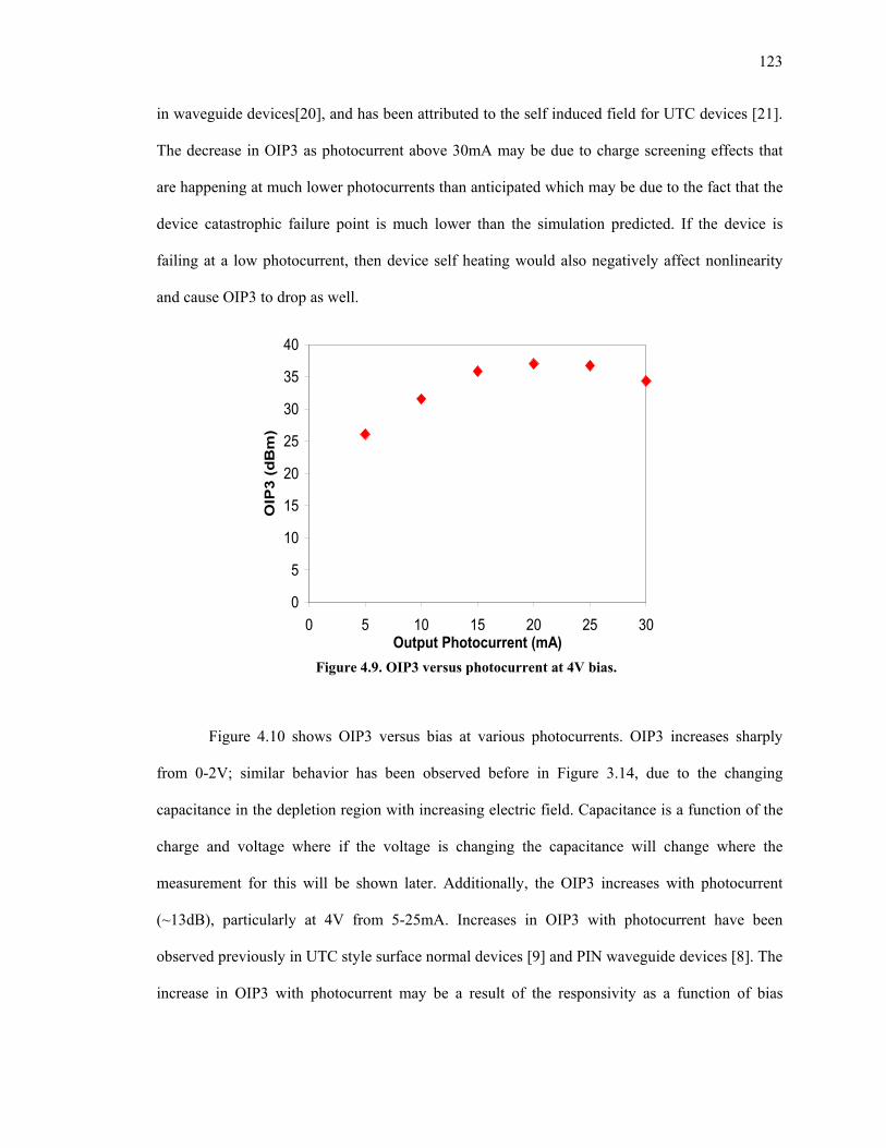
123
in waveguide devices[20], and has been attributed to the self induced field for UTC devices [21].
The decrease in OIP3 as photocurrent above 30mA may be due to charge screening effects that
are happening at much lower photocurrents than anticipated which may be due to the fact that the
device catastrophic failure point is much lower than the simulation predicted. If the device is
failing at a low photocurrent, then device self heating would also negatively affect nonlinearity
and cause OIP3 to drop as well.
Figure 4.9. OIP3 versus photocurrent at 4V bias.
Figure 4.10 shows OIP3 versus bias at various photocurrents. OIP3 increases sharply
from 0-2V; similar behavior has been observed before in Figure 3.14, due to the changing
capacitance in the depletion region with increasing electric field. Capacitance is a function of the
charge and voltage where if the voltage is changing the capacitance will change where the
measurement for this will be shown later. Additionally, the OIP3 increases with photocurrent
(~13dB), particularly at 4V from 5-25mA. Increases in OIP3 with photocurrent have been
observed previously in UTC style surface normal devices [9] and PIN waveguide devices [8]. The
increase in OIP3 with photocurrent may be a result of the responsivity as a function of bias
0
5
10
15
20
25
30
35
40
0 5 10 15 20 25 30Output Photocurrent (mA)
OIP
3 (d
Bm
)

124
voltage being more linear (up to 175kV/cm) at higher photocurrents; however, since the devices
are measured at 1GHz, the thermal heating may not be the dominant issue. In order to confirm
that R(V) is the dominant nonlinearity we plan to continue measurements by using a bias
modulation measurement technique presented in [13]. Additionally, the increase in OIP3 may be
explained by the self-induced field that has been observed before in UTC devices [20]. In Figure
4.4 as photocurrent increases, there is an induced field in the p-absorber region where there is
graded doping. We can simulate the transit time limited 3dB bandwidth using Silvaco, by solving
for a particular current density and then applying a small signal to the optical beam to find the
device response. We simulated the second beam as a small signal starting at 1GHz frequency with
steps of 1GHz up to 100GHz. After simulating at multiple photocurrent densities we can extract
the frequency at which the device response has dropped 3dB. In Figure 4.11 we can see that as
the photocurrent density increases there is an increase in the 3dB bandwidth followed by a sharp
drop off at very high photocurrent densities, which is where the device is under saturation. This
increase in device response has been detailed before in UTC style waveguide devices [20].
Figure 4.10. OIP3 versus bias voltage at various photocurrents for 1GHz and 1.1GHz input tones.

125
Figure 4.11. Simulated transit time limited 3dB bandwidth as a function of photocurrent density for
DCPD at 4V bias (with no load).
Figure 4.12. Maximum device temperature vs. output photocurrent for DCPD as
designed and with 0.5µm undercut (with no load).
0
10
20
30
40
50
60
70
0 0.5 1 1.5 2
f 3dB
(GH
z)
Photocurrent Density (mA/um2)
300
350
400
450
500
550
600
0 50 100 150 200
Max
imum
Dev
ice
Tem
pera
ture
(K)
Output Photocurrent (mA)
UTC DCPD (designed)
UTC DCPD (with 0.5um undercut)

126
Since this is the first time that a DCPD has been demonstrated, it is as important to
understand its behavior as to show its performance. We were unable to reach the high
photocurrent predicted from simulations due to a fabrication defect that unintentionally reduced
the p-mesa width by 0.5µm due to undercutting. We believe the undercutting lead to self-heating
at a much lower power than anticipated. To investigate this issue we first thermally simulated the
undercut and compared it to the original device simulation from Figure 4.6. The results of the
simulation can be seen in Figure 4.12, where we see the device undercut causes failure at a much
lower photocurrent (about 30%) than our original (and best case scenario). Next we compared
previous waveguide photodiodes from [21] and the DCPD to see where failure occurred in the
device. In Figure 4.13a the device is 5µm wide and the catastrophic failure clearly occurs at the
front of the device, with damage to both the p-mesa and p-metal. In contrast, in Figure 4.13b, the
DCPD shows about 10µm of metal at the front end before the failure occurs. In the case of the
DCPD, we were able to avoid catastrophic failure at the very front of the device. The damage is
mostly in the metal, rather than the mesa. From Figure 4.13b we show that the DCPD is capable
of relieving some of the front end current density compared to a traditional WGPD. Reducing the
p-absorber thickness and widening the p-mesa should help avoid the p-metal damage we see in
Figure 4.13b.

127
(a)
(b)
Figure 4.13. Images of catastrophic failure for (a) 5µm by 55µm PIN WGPD and (b) UTC-DCPD, note zoom levels are not equal.
Alternatively when considering improvements for the DCPD design in the future, other
detector structures such as the partially depleted absorber (PDA) [22] may perform better. The
PDA structure has currently demonstrated RF output of 26.5dBm, over 700mA of compression
current and a very high linearity figure of merit [23]. The device utilizes an InGaAs absorber in
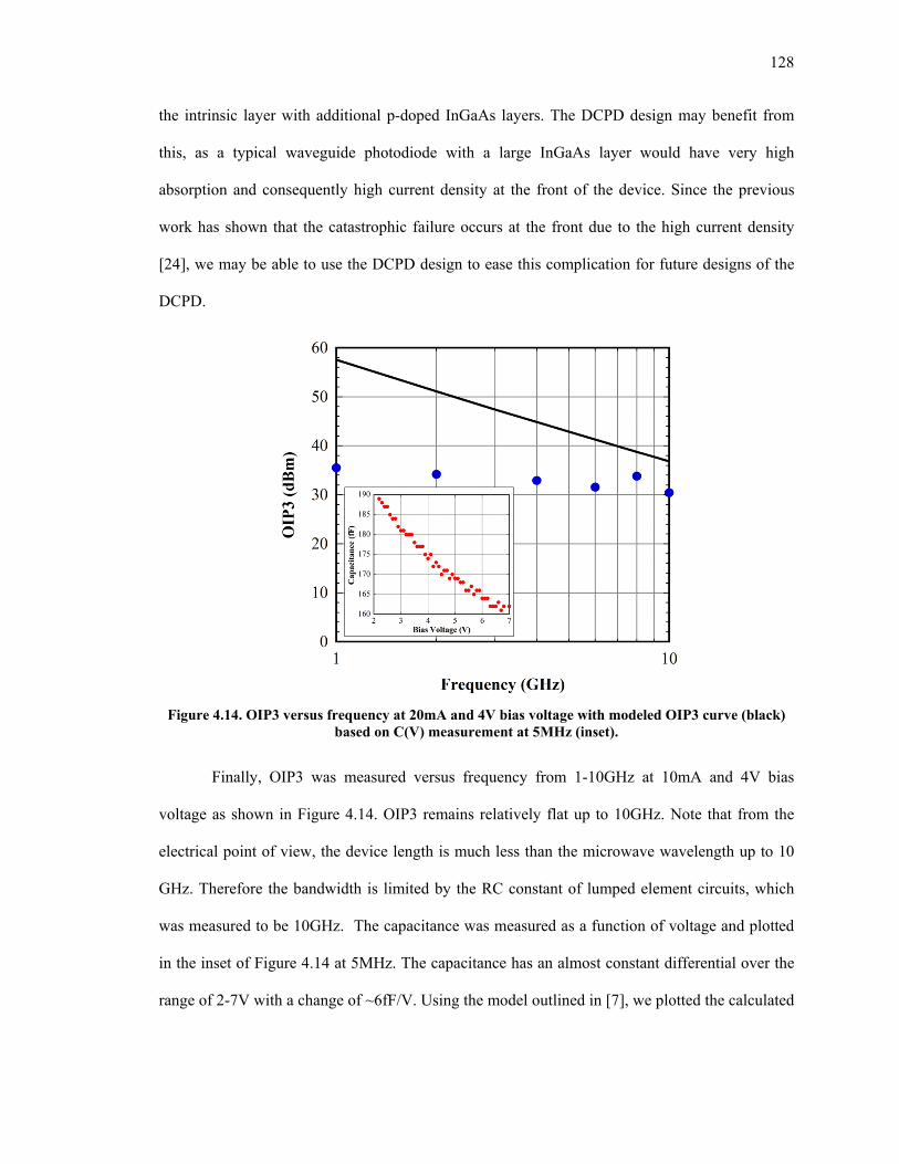
128
the intrinsic layer with additional p-doped InGaAs layers. The DCPD design may benefit from
this, as a typical waveguide photodiode with a large InGaAs layer would have very high
absorption and consequently high current density at the front of the device. Since the previous
work has shown that the catastrophic failure occurs at the front due to the high current density
[24], we may be able to use the DCPD design to ease this complication for future designs of the
DCPD.
Figure 4.14. OIP3 versus frequency at 20mA and 4V bias voltage with modeled OIP3 curve (black)
based on C(V) measurement at 5MHz (inset).
Finally, OIP3 was measured versus frequency from 1-10GHz at 10mA and 4V bias
voltage as shown in Figure 4.14. OIP3 remains relatively flat up to 10GHz. Note that from the
electrical point of view, the device length is much less than the microwave wavelength up to 10
GHz. Therefore the bandwidth is limited by the RC constant of lumped element circuits, which
was measured to be 10GHz. The capacitance was measured as a function of voltage and plotted
in the inset of Figure 4.14 at 5MHz. The capacitance has an almost constant differential over the
range of 2-7V with a change of ~6fF/V. Using the model outlined in [7], we plotted the calculated

129
capacitance limited OIP3 for the device, which is plotted in Figure 4.14. We can see from this
that the data follows the calculated limit at frequencies above 6GHz.
4.4 Device Variations
4.4.1 Variation Designs
In addition to the device introduced in section 4.3, additional device variations were
introduced, including the width of the MMI coupler (8µm in the baseline design) and the width of
the PD or p-mesa (2µm baseline). For the MMI mesa, the device variations included widths of
6µm, 7µm, 9µm and 10µm, in addition to the baseline structure. Additionally, the device had PD
width variations of 2.5µm, 3µm, 4µm and 5µm, only PD widths from 2.5µm to 4µm will be
analyzed.
4.4.2 Thermal Simulation
In order to get an initial understanding of variations on certain device dimensions we
performed thermal simulations using Comsol. In each case we modified the device dimensions
accordingly. Additionally we modified the power density distribution we'd expect for each device
dependent on the dimensions. In our simulation we account only for uniform power density
throughout the intrinsic region, where the heat is generated. This is a best case scenario for each
device, as we know altering both the MMI width and PD width will significantly change the
absorption profile. This simulation will give us a general understanding the basic thermal
limitations we will have from changing the device geometry.
In Figure 4.15 we plot the maximum device temperature versus output photocurrent for
varying MMI widths. We can see from the figure that varying the MMI width has little impact on
the overall temperature of the device and generally the temperature decreases linearly with MMI

130
width. We only expect a small change in temperature since the heat is primarily generated in the
PD mesa, although some of the intrinsic layers are part of the MMI. Since the absorption occurs
in the p-mesa we expect that the carrier density that will result will occur directly below the p-
absorber in the intrinsic region. The heat distribution and absorption profile will be more heavily
affected by the change in coupling properties that will occur with the change in MMI width and
to an extent the changing PD width as this will change the balance of the MMI. In the next
section we will look at the responsivity and discuss this behavior.
Figure 4.15. Thermal simulation of maximum device temperature vs. output photocurrent for
varying MMI widths at 4V bias with no load.
300
350
400
450
500
550
600
0 50 100 150 200
Max
imum
Dev
ice
Tem
pera
ture
(K)
Output Photocurrent (mA)
6µm7µm8µm (basline)9µm10µm

131
Figure 4.16. Thermal simulation of maximum device temperature vs. output photocurrent for
varying PD widths at 4V bias with no load.
In Figure 4.16 we plot the maximum device temperature versus output photocurrent for
varying device width. In this case we see a large increase in output photocurrent capability from
2µm to 2.5µm, but only a small increase from 2.5µm to 3µm.The discrepancy between the two
may explained by this. As the width goes from 2 to 2.5, the reduction in power density reduces
the thermal load and reach higher photocurrent before 600K; however when the device with goes
from 2.5 to 3, there is a smaller percentage increase in device area, as well as more of a thermal
barrier. Figure 4.17 plots the top down view of each device at 150mA output photocurrent. We
can clearly see that the 2.5µm device has better lateral thermal heat distribution than 3µm. The
reason for this is the geometry of the two devices. Since the MMI width is not changing below
the absorber the MMI extends out 1.5µm wider (below the absorber on one side) for the 2.5µm
device, so that the heat can spread laterally and down into the substrate easily. In the case of the
3µm device there is only 1µm of the MMI for the heat to extend laterally before it hits the corner
300
350
400
450
500
550
600
0 100 200 300 400
Max
imum
Dev
ice
Tem
pera
ture
(K)
Output Photocurrent (mA)
2µm (baseline)2.5µm3µm4µm

132
of the MMI mesa layer. This corner creates a thermal barrier. In the case of the 4µm wide device
this corner no longer exists since now the edge of the p-layers line up with the MMI layers, thus
making the path of least thermal resistance only the downward direction (into the substrate).
Figure 4.17. Top down view at 150mA output photocurrent for varying PD width at 4V bias with no
load.
4.4.3 Responsivity Measurement
Responsivity for each device was measured from 0-4V, shown in Figure 4.18 and Figure
4.19 for MMI width and PD width variations respectively, with the baseline device indicated with
solid data points. In Figure 4.18 the overall responsivity has no clear trend either up or down

133
with MMI width. This indicates that the device responsivity has a complex dependence on the
modal structure in the MMI and thus the absorption profile will be significantly affected by MMI
dimensions (delay length and width, and input waveguide position). Not only does this change in
absorption profile affect responsivity, but previous waveguide structures have shown that
lowering and spreading out the current density significantly affects the thermal characteristics of
the device and consequently OIP3 as detailed in [21]. In Figure 4.19, responsivity increases with
increasing absorber width. This behavior is reasonable since the device absorption area is
increasing with width. There is a large jump between 2µm and 2.5µm, but little change from
2.5µm to 3µm. An explanation for this is that the increase in width of the PD allows for more
absorption, but also changes the coupling factor which may cancel out the increase in this
instance caused by larger absorption area.
Figure 4.18. Responsivity versus bias voltage at 20mA photocurrent for DCPD devices with varying
MMI widths, and a fixed MMI delay length.

134
Figure 4.19. Responsivity versus bias voltage at 20mA photocurrent for DCPD devices with varying
PD (p-mesa) widths.
The general behavior of responsivity versus bias voltage is similar for all devices, where
there is a large increase in responsivity from 0-1.5V and then a leveling off from 1.5-4V. The
increase in responsivity from 0-1.5V results from the increase in electric-field across the
depletion region as bias is applied, which will counteract the space-charge nonlinearities which
occur at high photocurrent (20mA). After reaching the point at which there is a significant electric
field (>40kV/cm) across the device, temperature dependent effects due to band-gap shifting may
occur, where the responsivity may increase or decrease depending of the shift in the bandgap
which will cause a change in the absorption coefficient [12].
From Figures 4.18 and 4.19 we conclude that nonlinearity of the responsivity changes as
a function of the device geometry and thus the nonlinearities will result accordingly. The
analytical relationship between the nonlinear voltage-dependent responsivity and OIP3 as a
function of MMI and PD width will be discussed in the next section.

135
4.4.4 Bandwidth Measurement
The bandwidth for each device variation was measured similarly as in 4.3.3. The
bandwidth versus the width of the MMI coupler can be seen in Figure 4.20 along with the
calculated RC bandwidth. The bandwidth was calculated by taking the capacitance of the
photodiode adding the parasitic capacitance due to both the benzocylobutane (BCB) polymer
bridge on which the p-metal sits and metal conductors of the coplanar waveguide (CPW) and
using . The parasitic capacitance calculated was 21fF and the device capacitance
was 116fF. In the case of the MMI width changing we do not expect to see any change in the
bandwidth since we are changing a parameter that is passive. The photodiode mesa is unchanged
in this situation. Comparing the device to the rough calculation we see that the bandwidth is about
10GHz lower, which indicates that there is more parasitic capacitance than our initial calculation
gives us. In Figure 4.21 the 3dB bandwidth versus PD width is plotted along with the calculated
bandwidth. In this case we should see a significant change in bandwidth (as evident in our
calculation), however the 3dB bandwidth only changes by ~1.5GHz. Since in this case the
metallization and dimensions of our CPW we would need to calculate the parasitic capacitance in
more detail for each case in order to get an accurate model.

136
Figure 4.20. 3dB bandwidth versus MMI coupler width for DCPD devices with calculated in black.
Figure 4.21. 3dB bandwidth versus PD width for DCPD devices with calculated in black.
4.4.5 Voltage-Dependent Nonlinearities
The voltage-dependent responsivity has been discussed before by Hastings et al. in [12].
The authors used a second order polynomial expansion to predict the second order distortions as
0
5
10
15
20
25
5 6 7 8 9 10 11
3dB
(GH
z)
MMI Coupler Width (µm)
0
5
10
15
20
25
1.5 2.5 3.5 4.5
3dB
(GH
z)
PD Width (µm)

137
related to the voltage-dependent responsivity nonlinearity measured. This analysis can be
extended to predict the third order distortions. Depending on the shape of the curve and the range
of data being analyzed, using a third order polynomial may or may not be sufficient to predict
third order distortions. In some cases it may be necessary to use higher order polynomials in order
to accurately predict second and third order nonlinearities. For our analysis we will consider a
photocurrent with the form
(4.1)
where is the responsivity in the absence of any nonlinearity with units A/W, is the first-
order voltage-dependent responsivity with units of A/W/V, and is the second-order voltage-
dependent responsivity with units of A/W/V2. Equation (4.1) can be used to determine the
relationship between the third-order distortion and the fundamental power. As in [12], for a small
nonlinearity the dynamic voltage drop across the photodiode is defined as
(4.2)
where Z is the load impedance. The incident power can be defined as
(4.3)
where is the average power and is the modulation depth. Substituting (4.3) and (4.2) into
(4.1), the relationship between the third order and fundamental power can be obtained
Using (4.4), OIP3 can be related to the voltage-dependent responsivity nonlinearities
discussed in 4.4.2 for the various devices measured. A change in the nonlinear responsivity
behavior of each device can be fitted with a polynomial and coefficients c1 and c3 can be

138
extracted, which represent the voltage dependent nonlinearites of the first and third order caused
by avalanching, thermal and possibly other unknown effects. For the baseline device we extracted
from 2V to 4V values of c1=0.6284 (A/W), c2=0.0424 (A/W/V) and c3=0.0054 (A/W/V2).
Comparing our value of c2 to [12] which was 0.002 (A/W/V) we have an little over an order of
magnitude higher value which would indicate more second order nonlinearities. This may be due
to the fact that we are operating at a much higher photocurrent (compared to [12]) which will be
affected by linearities such as band gap shifting due to thermal heating. Additionally, the
capacitance will play a siginificant factor in determining nonlinearity, especially at higher
frequencies.
OIP3 was measured using the setup outlined in 2.3.3, with fundamental tones of 1GHz
and 1.1GHz. The assumption is that the OIP3 will still be in the quantum efficiency (responsivity)
limited range at this frequency since the baseline device has a 3dB bandwidth of 10GHz. The
device with a 6µm wide MMI coupler was measured at 4V bias and 20mA photocurrent. The
output RF fundamental power and third-order intermodulation distortion (IMD3) RF power,
occuring at 0.9GHz, is shown in Figure 4.22 for various modulation depths as a function of
output fundamental RF power. Fitting curves have been added and extracted to the intercept
point, giving an OIP3 of 36.8dBm, where the IMD3 has a slope of three and the fundamental has
a slope of one. The rest of the devices were measured in a similar manner.

139
Figure 4.22. Output fundamental RF power and third order distortion RF power versus output
fundamental RF power for the DCPD device with 6µm wide MMI at 4V bias and 20mA photocurrent.
Figure 4.23. Extracted c1 and c3 parameters versus MMI width from Figure 4.18.
OIP3= 36.8dBm

140
Figure 4.24. OIP3 (measured: solid, calculated: open) versus MMI width at 20mA and 4V bias.
The parameters c1 and c3 can be extracted by taking a second-order polynomial fit of the
curves in Figure 4.18 from 1-4V where the value of each are plotted in Figure 4.23. The
calculated OIP3 was extracted using |c1| and |c3| from the plot with Z=50 and OIP3 is independent
of A and m. The nonlinearity parameters generally vary in coordination with each other, however
for the 10µm device |c1| decreases but |c3| increases in which case |c3| should be the dominant
factor in OIP3. The result can be seen along with the measured values in Figure 4.24. The
calculated data shows similar behavior versus MMI width suggesting that the voltage-dependent
nonlinearity is a dominating factor. In the case of 6µm width the calculation is ~3dB lower in
which case we may need to include other nonlinearities in order to more accurately model OIP3.
In the case of the 10µm device the OIP3 decreases confirming our earlier prediction that the
decrease in |c3| would dominate the increase in |c1| . As OIP3 varies nonmonotonically with MMI
width a number of factors could be the cause, such as thermal variations due to the change in

141
absorption profile. We can recall the responsivity in Figure 4.18 also varied nonmonotonically
with MMI width.
Figure 4.25. Extracted c1 and c3 parameters versus photodiode width from Figure 4.19.
For the second set of variations, PD width, similar analysis has been completed to extract
c1 and c3 from Figure 4.19 which is plotted in Figure 4.25. Additionally, the OIP3 and calculated
OIP3 is plotted in figure 4.26. The same relationship between the two is noted as in Figure 4.24.
In Figure 4.26, the highest OIP3 is not the baseline device, but the 3µm wide PD, which
corresponds to the lowest value of c3 in Figure 4.25. When looking back at the thermal
simulations, the 2.5µm device had the best lateral heat distribution, however this device also has
the lowest OIP3. There are many factors that will trade off in this particular device, as the
absorption profile is also different, where the distribution of current may cause unwanted
nonlinearities in this case so it is too early to make a concrete conclusion for the drop in OIP3 for
this device. At low photocurrents, the nonlinear thermal effects will be negligible. Although we
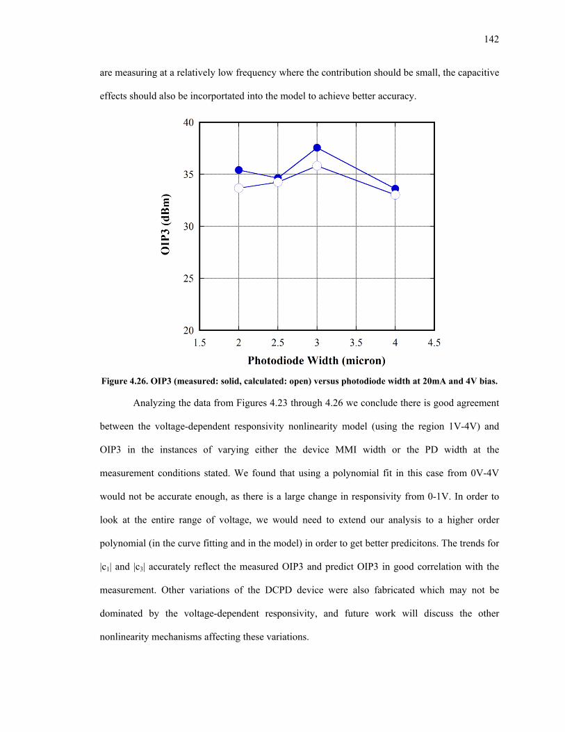
142
are measuring at a relatively low frequency where the contribution should be small, the capacitive
effects should also be incorportated into the model to achieve better accuracy.
Figure 4.26. OIP3 (measured: solid, calculated: open) versus photodiode width at 20mA and 4V bias.
Analyzing the data from Figures 4.23 through 4.26 we conclude there is good agreement
between the voltage-dependent responsivity nonlinearity model (using the region 1V-4V) and
OIP3 in the instances of varying either the device MMI width or the PD width at the
measurement conditions stated. We found that using a polynomial fit in this case from 0V-4V
would not be accurate enough, as there is a large change in responsivity from 0-1V. In order to
look at the entire range of voltage, we would need to extend our analysis to a higher order
polynomial (in the curve fitting and in the model) in order to get better predicitons. The trends for
|c1| and |c3| accurately reflect the measured OIP3 and predict OIP3 in good correlation with the
measurement. Other variations of the DCPD device were also fabricated which may not be
dominated by the voltage-dependent responsivity, and future work will discuss the other
nonlinearity mechanisms affecting these variations.
143
4.5 Conclusion
A novel DCPD device has been presented. The device exhibits a maximum responsivity
of 0.88A/W and OIP3 of 35dBm at 4V and 25mA. The device linearity was measured over a
range of frequencies and photocurrents. The design allows for coupling that reduces the front
facet current density, where the failure point was shown to no longer occur at the front of the
device, as was the case with a WGPD. Simulation results indicate that absorption per unit length
in UTC detector could even be much lower than the 1% incident power reported here. The
smaller the fraction of absorbed power per unit length, the larger is the total power that can be
detected without saturation. A smaller fraction of the absorbed power implies much longer length
will be required to achieve a respectable responsivity. This implies that, with proper design, the
power handling capacity of DCPD can be very large, without limiting bandwidth.
Additionally, variations on the baseline UTC DCPD including MMI width and PD width
were characterized. The devices were simulated thermally and we determined that the device
geometry plays an integral roll in the thermal distribution of the device. We found that from a
best base scenario, the 2.5µm wide device had very good thermal distribution in the lateral
direction; however more modeling will need to be completed to account for the nonlinear
capacitance contribution to nonlinearity. The device bandwidths were measured and compared to
the theorical curves. Also an analyic model for voltage-dependent responsivity nonlinearities
demonstrated good correlation for the devices. The device responsivities were measured from 0-
4V bias at 20mA in order to extract the model parameters, which were then used to predict OIP3.
OIP3 was measured at 20mA and 4V for each device and the calculated OIP3 was plotted as well.
The analysis is still preliminary and continued work, including a more rigorous look at
responsivity that includes an AC component will help us to better understand the various
nonlinearity mechanisms that are present in the DCPD device.

144
We were able to successfully demonstrate the ability to control the absorption profile
along a waveguide photodiode without the cost of bandwidth which was the method used in
Chapter 3 where the absorber was thinned and the device lengthened. Although there are other
ways to alter the absorption profile without the change in bandwidth, as demonstrated by the
refracting facet photodiode [1]. From the first demonstration of the device, we have concluded
there are significant power limitation issues, since we still have failure relatively close to the front
end of the device. The use of alternatives for future designs, such as the PDA or thinning the p-
absorber were suggested as a way to avoid some of the perturbation of the directional coupler and
possibly increase power handling capability. We also determined that the 2µm width device is
very sensitive fabrication tolerances even with a small undercut, while the 3µm device provided
the highest linearity. Although the linearity of the device was not as high as we initially expected,
we learned a lot from the design variations where the DCPD is a complicated structure, as the
linearity does not change monotonically with either the PD or MMI widths. Since the absorption
profile and device behavior can change drastically for small changes in these parameters, for
future generations we will need to do extensive simulation for the design and incorporate the data
obtained through our investigations. Additionally we will need to look at the nonlinear
capacitance and in order to model more accurately the OIP3, especially at high frequencies.
Although the responsivity plays an important role in the nonlinearity of the device, the
capacitance is a just as important and will need to be a major design factor in the future.
Designing a slightly wider device, and the MMI structure accordingly, while slightly thinning the
absorber should improve the device performance in future generations.

145
4.6 Acknowledgments
Portions of Chapter 4 appear in "Novel Directional Coupled Waveguide Photodiode -
Concept and Preliminary Results," published in Optics Express, vol. 18, no. 17, pp. 17729-17735
(2010), Meredith N. Draa, J. Bloch, D. Chen, D. C. Scott, N. Cheng, S. B. Chen, X. Yu, W. S.
Chang, P. K. L. Yu, and "Voltage-Dependent Nonlinearities in Uni-Traveling Carrier Directional
Coupler Photodiodes" accepted to the 2010 IEEE International Topical Meeting on Microwave
Photonics (2010), Meredith N. Draa, J. Bloch, W. S. Chang, P. K. L. Yu, D. C. Scott, N. Chen S.
Chen, and K. J. Williams. The contributions to the DCPD design, including the directional
coupled waveguide and CPW design, by Jeffrey Bloch, Dingbo Chen and Xuecai Yu are greatly
appreciated. Contribution from co-authors Dr. David C. Scott is greatly appreciated for the
fabrication of the devices and RF response measurements. The author would also like to
acknowledge the insight and guidance provided by Professors Paul Yu, William Chang and Dr.
Keith Williams as well as funding support through DARPA from both Dr. Steve Pappert and Dr.
Ron Esman. The author of this thesis was the primary author of this work.

146
4.7 References
[1] T. Ohno, H. Fukano, Y. Muramoto, T. Ishibashi, T. Yoshimatsu, and Y. Doi,
“Measurement of intermodulation distortion in a unitraveling-carrier refracting-facet photodiode and a p-i-n refracting facet photodiode,” IEEE Photon. Technol. Lett., vol. 14, 375-377 (2002).
[2] J. Klamkin, Y.-C. Chang, A. Ramaswamy, L. A. Johansson, J. E. Bowers, S. P. DenBaars, and L. A. Coldren, "Output saturation and linearity of waveguide unitraveling-carrier photodiodes," IEEE J. Quantum Electron., vol. 44, pp. 354-359 (2008).
[3] S. Demiguel, N. Li, X. Li, X. Zheng, J. Kim, J. C. Campbell, H. Lu, and A. Anselm, "Very high-responsivity evanescently coupled photodiodes integrating a short planar multimode waveguide for high-speed applications," IEEE Photon. Technol. Lett., vol, 15, pp. 1761-1763 (2003).
[4] A. Umbach, D. Trommer, R. Steingruber, A. Seeger, W. Ebert, G. Unterborsch, "Ultrafast, high-power 1.55µm side-illuminated phtoodetector with integrated spot size converter," in Optical Fiber Communication conference, 2000 OSA Technical Digest Series (Optical Society of America, 2000), paper FG2-1.
[5] M. N. Draa, J. Bloch, D. C. Scott, N. Chen, S. B. Chen, W. S. C. Chang, and P. K. L. Yu, “Behaviors of the third order intercept point for a p-i-n waveguide photodiode,” Optics Express, vol. 17, no. 16, pp. 14389-14394, 2009.
[6] V. J. Urick, A. S. Hastings, J. D. McKinney, P. S. Devgan, C. Sunderman, J. F. Diehl, K. Colladay and K. J. Williams, “Photodiode Linearity Requirements for Radio-Frequency Photonics and Demonstration of Increased Performance Using Photodiode Arrays,” 2008 Int. Meeting Microwave Photonics Digest, pp. 86-89, Oct. 2008.
[7] H. Jiang and P. K. L. Yu, “Equivalent circuit analysis of harmonic distortions in photodiodes,” IEEE Photon. Technol. Lett., vol. 10, no. 11, pp. 1608–1610, Nov. 1998.
[8] M. Draa, J. Ren, D. C. Scott, W. S. Chang, and P. K. L. Yu, “Frequency behaviors of the third order intercept point for a waveguide photodiodes using a three laser two-tone setup,” 2008 IEEE LEOS, Long Beach, .. 284-285.
[9] H. Pan, Z. Li, A. Beling, and J. C. Campbell, “Measurement and modeling of high-linearity modified uni-traveling-carrier photodiode with highly-doped absorber,” Optics Express, vol. 17, no. 22, pp. 20221-20226, Oct. 21, 2009.
[10] K. J. Williams, R. D. Esman, and M. Dagenais, “Nonlinearities in p-i-n microwave photodetectors,” IEEE J. Lightw. Technol., vol. LT-14, no. 1, pp. 84-96, Jan. 1996.

147
[11] R. R. Hayers and D. L. Persechini, “Nonlinearity of p-i-n photodetectors,” IEEE Photon. Technol. Lett., vol. 5, no. 1, pp. 70-72, Jan. 1993.
[12] A. Hastings, D. A. Tulchinsky, and K. J. Williams, “Photodetector Nonlinearities Due to Voltage-Dependent Responsivity,” IEEE Photon. Technol. Lett., vol. 21, no. 21, pp. 1642-1644, Nov. 1, 2009.
[13] H. Pan, A. Beling, H. Chen, and J. C. Campbell, “The Frequency Behavior of Intermodulation Distortions of Modified Uni-Traveling Carrier Photodiodes Based on Modulated Voltage Measurements,” IEEE J. Quantum Electron., vol. 45, no. 3, pp. 273-277, Mar. 2009.
[14] H. Pan, A. Beling, and J. C. Campbell, “High-Linearity Uni-Traveling-Carrier Photodiodes,” IEEE Photon. Technol. Lett., vol. 21, no. 24, pp. 1855-1857, Dec. 15, 2009.
[15] Z. Li, H. Chen, H. Pan, A. Beling, and J. C. Campbell, “High-Power Integrated Balanced Photodetector,” IEEE Photon. Technol. Lett., vol. 21, no. 24, pp. 1858-1860, Dec. 15, 2009.
[16] Srivastava, Shivani, “Simulation Study of InP-Based Uni-Traveling Carrier Photodiode” Masters Thesis, University of Cincinnati (2003).
[17] Siklitsky, Vadim, "Electronic Archive: New Semiconductor Materials. Characteristics and Properties," Ioffe Physico-Technical Institute http://www.ioffe.rssi.ru/SVA/NSM/.
[18] X. Wang, N. Duan, H. Chen, and J. C. Campbell, "InGaAs-InP Photodiodes with High Responsivity and High Saturation Power," IEEE Photon. Technol. Lett., vol. 19, no. 16, pp. 1272-1274 (2007).
[19] N. Shamir and D. Ritter, “Low Electric Field Hole Impact Ionization Coefficients in GaInAs and GaInAsP,” IEEE Electron Device Lett., vol. 21, no. 11, pp. 509-511, Nov. 11, 2000.
[20] J. Klamkin, A. Ramaswamy, Y.-C. Chang, L. A. Johansson. M. M. Dummer, J. E. Bowers, S. P. DenBaars, and L. A. Coldren, "Uni-traveling-carrier photodiodes with increased output response and low intermodulation distortion," in Proc. of IEEE International Topical Meeting on Micro. Photon. (IEEE, 2007), pp. 14-17.
[21] M. N. Draa, J. Bloch, D. C. Scott, N. Chen, S. B. Chen, W. S. C. Chang, and P. K. L. Yu, “Behaviors of the third order intercept point for a p-i-n waveguide photodiode,” Optics Express, vol. 17, no. 16, pp. 14389-14394, 2009.
[22] A. Beling, H. Pan, H. Chen, and J. C. Campbell, “Measurement and modeling of high-linearity partially depleted absorber photodiode,” Electon. Lett., vol. 44, no. 24, Nov. 20, 2008.

148
[23] D. A. Tulchinsky, J. B. Boos, D. Park, P. G. Goetz, W. S. Rabinovich, and K. J. Williams, “High-current photodetectors as efficient, linear, and high-power RF output stages,” IEEE J. of Lightwave Technol., vol. 26, 408-416 (2008).
[24] H. Jiang and P. K. L. Yu, “Waveguide integrated photodiode for analog fiber-optic links,” IEEE Trans. Microwave Theory and Techniques. vol. 48, pp. 2604-2610 (2000).

149
Chapter 5 Conclusion and Future Work
5.1 Summary
The primary motivation behind this thesis was to answer the questions, "How can we
accurately measure nonlinearity in photodiodes, and how can we use this to characterize devices
in order to investigate the nonlinearity of different device designs through analytical models?"
The first step in answering this question was to analyze our current nonlinearity measurement
setup and detect if there were any inherent non-ideal factors that cause measurement inaccuracies.
It is only thorough mitigating these factors that we hope a new system can be developed to
measure future devices. The accurate measurement is important for the characterization of high
linearity photodiodes, used in two designs, a PIN waveguide and a UTC DCPD design. In order
to characterize our devices and investigate nonlinearities, the measurement system accuracy is
critical to investigations we perform in order to obtain a better understanding of the nonlinearity
mechanisms. The research presented in this dissertation is one small part of the overall
understanding of nonlinearities and the phenomena that contribute unwanted distortions.
First, the contributed nonlinearities of the current measurement system were discussed.
From this the three-laser two-tone measurement system was designed in order to control the
unwanted MZM nonlinearity. We were able to show the contributed MZM nonlinearities and
established that they could be distinguished from the photodiode nonlinearity. The data presented
was backed up with the mathematical analysis of the system, confirming the measured slope
relationships. From the new system we concluded that the use of the extra laser to provide a
consistent DC optical power, while using the VOAs to control modulation depth allowed for the

150
MZM nonlinearities to be effectively controlled. We also looked at the OIP3 measurement of a
test photodiode using the one and two tone heterodyne setups and the four-laser three-tone MZM
setup. The three systems were used to measure the same device under the same conditions (bias
voltage, photocurrent, optical wavelength and frequency). The data was compensated between the
one, two and three-tone cases using mathematical relationships. From the data we concluded that
as long as the device exhibited a strong slope of three for third order distortion the data could be
compared across setups. The third order intermodulation distortions of the device however did not
always exhibit a slope of three due to possibly the presence of other competing nonlinearities,
resulting in vastly different OIP3 measurements for each system. The polarization of the optically
modulated beams was investigated and shown to affect the measurement in certain instances;
however we have not fully understood the measurement discrepancies between the three setups.
Second, two PIN waveguide photodiodes were presented in Chapter 3. The devices were
designed for high power high linearity analog optical links using a PIN layer structure with a
waveguide device geometry. The devices were the same design except that for device B the
absorber was half the thickness of device A and twice the length. The result was that device B
had half the bandwidth, but approximately twice the power dissipation capability. Additionally,
device B demonstrated an increase in OIP3 resulting from the reduction in optical overlap factor
which provided a more spread out absorption profile and an increase in OIP3. We believe that
reducing the optical overlap factor reduced the charge screening occurring in the device. The DC
saturation was characterized experimentally, which was modeled well using Silvaco showing that
device A was saturation limited and device B did not saturate before thermal runaway occurred at
2V bias. The reduction in charge screening can cause the device to no longer be saturation limited
in the DC measurement, as well as reduce the nonlinear distortions resulting in the increased
OIP3 that was measured. The OIP3 versus frequency for device A was also used with the circuit
model first introduced by Jiang in [1]. From the analytical model, we find that we would like a

151
very high junction resistance on the order of 200kΩ and above where this resistance is maintained
as a function of photocurrent (i.e. low differential junction resistance). In order to achieve high
OIP3 over bandwidth of the device we would like to keep the junction capacitance low, ideally on
the order of 10's of fF, while having the negative differential capacitance around 8fF/mA if
possible. The circuit analysis of device A allowed us to theoretically look at different OIP3 curves
as a function of frequency. Ideally we would like the OIP3 curve to be as flat as possible versus
frequency (i.e. almost no roll-off). Our circuit model investigation indicates that the main
contributor to avoiding the roll-off is to achieve a low capacitance. Previous studies have shown
that creating a step-junction using high doping with dopants that have low diffusion at the p-i
interface improves the voltage-dependent capacitance and as a result the OIP3 at high frequencies
[2].
Third, a novel design developed by our group was presented that incorporated a
directional coupler with a UTC style waveguide photodiode. We observed through device failure
points along the device with photographs that the DCPD relieved the high current density at the
front end of the device when compared to a WGPD. The primary issue with the first design was
the low linearity measured. Since we do not need a thick absorber to achieve high responsivity, as
is the case with a surface normal device, removing the slightly n-doped absorbing layer should
help to improve our linearity. We also determined that there are still significant power limitations
for the first design, which can possibly be mitigated by decreasing the absorber thickness and
slightly widening the device, in coordination with a new MMI design to better balance the device.
We also thermally simulated device structures that varied the MMI width and absorber width,
finding that the 2.5µm width had the best lateral thermal distribution. Finally, the responsivity,
bandwidth and OIP3 were measured for the first generation device with varying MMI width and
absorber width. The bandwidth was modeled and we found the decrease in bandwidth with
increasing width was not as sharp as we predicted, possibly due to additional parasitic

152
capacitance. The OIP3 was analytically modeled using the responsivity data, which showed good
agreement with the data. We concluded from the data that the complexities of the DCPD make
OIP3 change non-monotonically with device changes in width of the MMI and PD.
5.2 Future Work
5.2.1 Nonlinearity Investigations
As discussed in Chapter 1, there are many contributing factors to the nonlinearity of a
photodiode. Some of these mechanisms include the fluctuation of carrier velocities and diffusion
constants which are influenced by space-charge fields, the flow of current in the p-contact,
scattering, and potential drops in the photodiode due to current flow in the external load
resistance [3]. Investigations have been performed to show the influence of the Franz-Keldysh
effect and impact ionization on the voltage-dependent responsivity [4]. Additionally, the voltage
and current dependent capacitance are major factors in nonlinearity which will be discussed in
more detail.
From the analysis presented in 4.4.3 we presented a correlation between voltage-
dependent responsivity nonlinearity and OIP3. Additionally there will be optical power dependent
responsivities which should be investigated. The voltage-dependent responsivity model showed
correlation with the measured general behavior of the OIP3 data as a function of MMI and
absorber width. This correlation suggests the same underlying mechanisms responsible for the
behaviors of the responsivity and OIP3. Another method for using this model is to calculate the
necessary values of parameters such as c3, which represent the third order nonlinearity, in order
to guide the design. Since designing the responsivity of the device is readily controllable we can
use this information to understand the tradeoffs between the two parameters. In order to be able to

153
use the model to design future devices we will need to identify the specific causes of nonlinearity
that will increase c3. Previously we mentioned the possibility of both impact ionization and
Franz-Keldysh effects which occur in the devices, where further investigation will allow us to
identify a specific cause of nonlinearity for our device using a physical model. Additionally, the
analytical model discussed in Chapter 4 can also be used to look at the second order nonlinearities
using the relationship from c1 and c2. After establishing an analytical relationship we can begin
to develop the physical models that correspond to the device mechanisms that are responsible for
nonlinearity. Previously, the second order relationship has been briefly discussed by Hastings et
al where they showed a good agreement using the model and the measurement of second order
harmonics [5]
Additionally nonlinear capacitance has been shown in [6], where the nonlinearity was
due to the sensitivity of the PD capacitance due to the charge location within the depletion region,
as a function of current. Capacitive nonlinearities can also result from external loading. Load
transients will cause the capacitance to change dynamically during the evolution of the current
waveform as it flows through the load impedance. When the device is biased and photocurrent is
induced through optical illumination a voltage drop is induced across both the series and load
resistances. The result of this voltage swing is a reduced bias voltage across the PD junction
causing variations in device capacitance [4]. The importance of diffusion of dopants in the p-
InGaAs region of a UTC device has been shown to negatively affect the voltage-dependent
capacitance and contribute to the IMD3 thus creating a need to ensure minimal diffusion in order
to avoid the nonlinearity contributions due to voltage swing from voltage dependent capacitance
[4]. Additionally, nonlinear capacitance results from the screening of the space charge field which
is dependent on photocurrent. At high illumination the total volumetric charge density in the
depletion region may change as a result of the preferential screening of both ionized donors and
acceptors by the free electrons and holes respectively [4]. The result of this neglecting feedback is

154
a deeper penetration of the depletion region into the quasi-neutral region [4]. These issues as well
as the previous mentioned responsivity nonlinearities are two areas that continue to warrant
investigation in order to better understand the photodiode behaviors.
5.2.2 Nonlinearity Modeling
We have used multiple software programs to model device behavior. Additionally there
are other modeling options. Currently none of the models combine the waveguiding modeling
provided by Beam Prop with the electrical modeling handled by Silvaco and the thermal
modeling provided by Comsol. To get an accurate picture of the device, developing a
combination of the three would be more useful, but Silvaco still has limited dynamic modeling
capabilities. Other software may be more useful, such as Crosslight Apsys which has the
capability to input two-tone signals and model the resulting behavior. Currently an absorption
profile can be modeled well in Beam Prop, shown in Figure 5.1 with a polynomial fit. The result
can be modeled as a function using a curve fit or possibly encoded into a file to input into Comsol
as the power distribution for the thermal simulation. The combination of these two programs
would give a better understanding of how much hot spots affect the heating distribution and
power dissipation limitations. Providing this level of simulation detail could sort out thermal
issues and provide better understanding of how to utilize heat sinking. Another benefit that could
be incorporated into the simulations is to take detailed photos of the devices after to extract better
measurements for the real device dimensions and contact thicknesses and determine points of
failure. An example of this is shown in Figure 5.1 of device A that was characterized in chapter 3.
Adding these changes to the Comsol simulation could provide useful understanding of how
fabrication tolerances can affect the power handling. Currently, the simulation predictions are far
above what the actual performance yielded for expected power dissipation. Finding a solution to
this problem for waveguide style photodiodes continues to be a necessarily and important topic.

155
Figure 5.1. Simulated DCPD power absorption along length of the device with polynomial fit (black).
0
0.002
0.004
0.006
0.008
0.01
0.012
0 50 100 150 200
Frac
tion
of P
ower
Abs
orbe
d (m
icro
n-1)
Position Along Absorber (micron)

156
(a)
(b)
Figure 5.2. Photo of device A before failure (a) and after catastrophic failure (b).
5.2.3 Redesigning the UTC DCPD
The first design of the DCPD device proved to be a novel concept that could vastly
improve the power dissipation capability of waveguide style devices. The device performed under

157
the expected benefits of the device, and some of those factors were discussed, such as fabrication
issues. From here the device will need to be redesigned. First, the device design should focus on
how to improve the linearity. Since we are using a waveguide design and do not require a thick
absorber for high responsivity, the lightly n-doped absorber that is in the intrinsic region is not
necessary. We also maybe like to investigate using a PIN structure as we saw good linearity for
device B in chapter 3. Again the UTC structure has shown high linearity for SN devices and is
beneficial to that geometry because there can be a thick absorber and thin intrinsic region.
Secondly we need to improve power dissipation. The narrow mesa obviously presented a
problem, and make fabrication difficult. Moving back to a 3µm or 4µm wide detector might help
relax some of the issues that occurred with the first generation device. In order to change the
device width we will have to redesign the layer structure and dimensions of the coupler for
effectively coupling to the absorber. As mentioned earlier, possibly moving to a PIN structure or
a UTC structure which has a thinner absorber, the perturbation of the coupler will be less severe,
which will allows us to design the coupler for a shorter and wider device.
From chapter 3 we found that for a normal waveguide device thinning the absorber
region and lengthening the device resulted in significant improvement. Additionally device B was
a 10GHz device, while the DCPD was designed for 20GHz, it only yielded a bandwidth of
10GHz. In this case the two devices had similar bandwidths but very different performances.
What we can learn from this is that the very thick absorber (0.65µm) may have caused carrier
buildup at the p-i interface which results in charge screening effects. If the absorber can be
reduced, by removing the n-doped absorber and thinning each of the layers that have different
doping, while maintaining a good responsivity (~0.75A/W) the device may see much better
power dissipation results.
Another aspect to investigate is other types of detectors to use for the layer structure.
Currently, partially depleted absorbers (PDA) provide the highest output power and power

158
dissipation for photodiodes [5]. In this instance the absorbing material is partially p-doped,
partially intrinsic and partially n-doped, where the layer thicknesses correspond to balancing the
electron and hole concentrations in the intrinsic region. An example layer structure can be seen in
Figure 5.3. In this case the p-doped layers of InGaAs are graded in two steps, as is the n-doped
layers, but the p-doped layers are slightly thicker since electrons have a higher velocity and more
need to be injected into the intrinsic region to balance the holes. The other benefit to this design is
that there are no heterojunctions at the p-i and i-n interfaces to cause additional carrier buildup.
Figure 5.3. Bandgap diagram of layer structure for PDA style photodiode with bias applied across i-InGaAs layer. Horizontal is the layer thickness and vertical is the bandgap (not to scale).
5.3 Conclusion
The need for higher power and higher linearity photodiodes continues to be significant.
As laser technology improves, photodiodes need to be able to handle requirements for these links.
Innovative ideas such as the DCPD design will lead the way in exploring solutions for the next
generation of analog optical links. The study of linearity as a limiting factor in photodiodes still
has many areas that are uncharacterized and not well understood, which leaves open a multitude
of research to be completed in the field of analog photodiodes.

159
5.4 Acknowledgements
In Chapter 5, the photos in Figure 5.3 were provided by Dr. David Scott at Archcom
Technolgy, Inc. Additionally, Figure 5.2 is a repeat of the data presented in Chapter 4 provided
by Jeff Bloch.

160
5.5 References
[1] H. Jiang, D. S. Shin, G. L. Li, T. A. Vang, D. C. Scott, and P. K. L. Yu, “The frequency behavior of the third-order intercept point in a waveguide photodetector,” IEEE Photon. Technol. Lett., vol. 12, pp. 540-542 (2000).
[2] H. Pan, Z. Li, A. Beling, and J. C. Campbell, “Measurement and modeling of high-linearity modified uni-traveling carrier photodiodes with highly-doped absorber,” Opt. Express, vol. 28, pp. 1316-1322 (2010).
[3] K. J. Williams, R. D. Esman, and M. Dagenais, "Nonlinearities in p-i-n Microwave
Photodetectors," J. Lightw. Technol., vol. 14, no. 1, pp. 84-96 (1996).
[4] H. Pan, A. Beling, H. Chen, J. C. Campbell, and P. D. Yoder, "The Influence of Nonlinear Capacitance and Responsivity on the Linearity of a Modified Uni-Traveling Carrier Photodiode," IEEE Intern. Topical Meeting on Microwave Photonics (MWP 2008), Gold Coast, Australia, Oct. 2008.
[5] A. S. Hastings, D. A. Tulchinsky, and K. J. Williams, “Photodetector Nonlinearities Due to Voltage Dependent Responsivity,” IEEE Photon. Technol. Lett., vol. 21, no. 21, pp. 1643-1644 (2009).
[6] K. Williams and P. Goetz, "Photodiode Compression due to Current-Dependent Capacitance," Int. Topical Meeting on Microwave Photonics (MWP 2000), Oxford, UK, (Sept. 2000).
[7] D. A. Tulchinsky, X. Li, N. Li, S. Demiguel, J. C. Campbell, and K. J. Williams, "High-Saturation Current Wide-Bandwidth Photodetectors," IEEE Journal of Selected Topics in Quantum Eletronics., vol. 10, no. 4, pp. 702-708 (2004).
161
Appendix A
Silvaco Models
All of the equations presented in this appendix are from the Silvaco User's Manual
Volume I. For the simulations various models can be specified. For In1-x Gax Asy P1-y layers the
low field mobility is defined:
Where and are the low field mobilities. For high field mobilities a parallel electric field
dependence can be established where:
Where VSATN and VSATP are defined as:

162
Where the defaults are:
Variable ValueBETAN 2BETAP 1ALPHAN.FLD 2.40E+07ALPHAP.FLD 2.40E+07THETAN.FLD 0.8THETAP.FLD 0.8TNOMN.FLD 600TNOMP.FLD 600
And TL is the lattice temperature specified. Additionally a negative differential mobility model by
Barnes et. Al. for is defined as:
Where the defaults are:
Variable ValueECRITN 4.00E+03ECRITP 4.00E+03GAMMAN 4GAMMAP 1
All of the variables can be specified in the simulations. Additionally the InP and InGaAs
use appropriate low field mobility as opposed to (A.1). The models described are defined by the
parameters set according to the defaults listed or otherwise are user specified. For the purposes of
our simulations the parameters were specified as:

163
Parameter InGaAs InP Energy Gap .734 eV 1.35 eV
Electron Lifetime τn0 0.704 ns
NSRHN 7.134x1017 cm-3 Electron Mobility
μmax 11599 cm2/V·s 4917 cm2/V·s μmax 3372 cm2/V·s 0 Nc 8.9x1016 cm-3 6.4x1017 cm-3 α 0.76 0.46
Ecritn 3000 V/cm 11000 V/cm γn 4 4
Hole Mobility μmax 331 cm2/V·s 151 cm2/V·s μmax 75 cm2/V·s 20 Nc 1x1010 cm-3 7.4x1017 cm-3 α 1.37 0.96
Ecritp 4000 V/cm 4000 V/cm γp 1 1
Saturation Velocity (E) 2.5x10⁷ m/s 2.6x10⁷ m/s Saturation Velocity (H) 5x10⁶ m/s 6.6x10⁶ m/s Imaginary Refractive 0.075 0
Real Refractive 3.595 3.165 Electron Affinity 4.58 4.37

164
Appendix B
Harmonic Balance Calculation
The analysis presented in this appendix is an expansion of the analysis provided in [1].
We will start with the equation for the equivalent circuit model. We can calculate the voltage, V,
across the load as:
Where which represents the two RF current sources, Z(ω) is the
equivalent impedance of parasitic capacitance, series resistance and the load resistance. C1 is the
optical-power-dependent differential capacitance and R1 is the optical power dependent
differential resistance. C0 and R0 are the respective capacitance and resistance of the junction at a
given DC photocurrent. We will approximate assuming :
Substituting (A.2) into (A.1):
where .
We will use the harmonic balance method [source], where V can be expressed as:

165
We can insert (B.4) into (B.3) and use the orthogonality property of sine and cosine
functions to extract the coefficients. First we will find the linear equations for V51a and V51b which
represent the IMD3:
We can use (B.5) to solve for V51a and V51b:

166
Now we need to solve for , , , , , , , and .
If , we can assume and .
Solving for and we have:
We can solve for and from:
From (B.9) we have:
Where D is as defined in equation (B.6). Next we can solve for and :

167
From (B.10) we have:
Solving for and we have:
From (B.13) we get:
where and are equivalent to equation (B.10) by replacing ω1 with ω2 and as before
and .
Now that we have solved for all variables we can substitute (B.8), (B.10), (B.12) and
(B.14) into (B.6) and solve for and . Finally we can calculate the IMD3:
[1] H. Jiang and P. K. L. Yu, “Equivalent circuit analysis of harmonic distortions in photodiodes,” IEEE Photon. Technol. Lett., vol. 10, no. 11, pp. 1608–1610, Nov. 1998.
Copyright © 2022 FDOKUMEN