Design and fabrication of SU8 arrayed-waveguide gratings using multimode interference couplers
9
Design and fabrication of SU-8 arrayed-waveguide gratings using multimode interference couplers Yunpeng Zhu, Bo Yang, Yuqing Jiao and Daoxin Dai Centre for Optical and Electromagnetic Research, State Key Laboratory of Modern Optical Instrumentation, Zhejiang University, Hangzhou, China ABSTRACT An SU-8-based arrayed-waveguide gratings (AWG) device with multimode interference couplers (MMI) is designed and fabricated. The demonstrated MMI-AWG device has 4 channels and the channel spacing is 500GHz. The total insertion loss is about 22 dB, which mainly comes from the coupling loss (16dB) between the input/output waveguide and the fibers. The channel crosstalk between adjacent channels is about –12 dB which is close to the simulation result. Keywords: component, SU-8, arrayed-waveguide gratings, multimode interference coupler 1. INTRODUCTION In the past several decades, optical waveguide-based planar lightwave circuits (PLCs) have been widely investigated because of their excellent performances. It is well know that a small bending radius is desired for increasing the integration density of PLCs, which will reduce the cost through high-yield processes. It is popular to realize ultracompact PLCs by using waveguides with a high refractive index contrast, e.g., the silicon-on-insulator (SOI) nanowire waveguides 1 . However, the fabrication of Si nanowires is costly, because some expensive equipments are inevitably needed because E-beam or deep-ultraviolet lithography process is usually required. Although the fabrication process is greatly improved 2 , Si nanowires still often suffer from serious sidewall scattering loss. Moreover Si nanowires cannot work for visible range (which is desired for some sensing applications) due to the large absorption coefficient of silicon at the wavelengths smaller than 1.1 m. Concerning the applications for the range from visible light to near infrared, photosensitive polymer (e.g., SU-8) is a good alternative option for PICs due to the large transparent window 3 . In previous works, people have achieved low-loss SU-8 waveguides at various wavelengths, e.g., 0.019±0.003dB/mm @ 632.8 nm 4 , 0.07 dB/mm @ 830 nm, 0.08 dB/mm @ 1310nm and 0.3 dB/mm @ 1550nm 5 . The availability of SU-8 in a broad wavelength range makes it very useful for many applications, including optical sensing mentioned above. Furthermore, polymer usually has the advantages of high flexibility, low cost and an easy fabrication process. Recently, small SU-8 strip waveguides with air claddings have been demonstrated theoretically as well as experimentally 6 . This type of SU-8 optical waveguide has a relatively high due to the air cladding, which is consequently helpful to achieve a small bending radius 3 . In this paper, we present our work on an arrayed-waveguide gratings (AWG) based on SU-8 strip waveguides. AWGs have been widely used for DWDM system as (de)multiplexers or routers 7 . When using low optical waveguide, e.g., SiO 2 -on-Si buried optical waveguides, the AWG (de)multiplexer is usually very large (at the order of several cm 2 ) because of the large bending radius 8 . People have presented compact AWG devices by using high optical waveguides 9 . However, in this case, a considerable loss will be introduced due to the mode mismatch between the free propagation region (FPR) and the arrayed waveguides. Mohammad et al proposed a novel AWG structure, in which multimode interference (MMI) couplers are used to replace the FPR in a conventional AWG 10 . The MMI coupler is widely used as power splitter as well as combiner with the advantage of easy fabrication, low loss, compactness, large optical bandwith and relaxed fabrication tolerance 11 . Therefore, for an MMI-AWG, the light from the input waveguide could be split and coupled into the arrayed waveguide with a very low loss. In this paper, we demonstrate out work on SU-8 AWGs using MMI couplers. Passive Components and Fiber-based Devices VII, edited by Perry P. Shum, Proc. of SPIE-OSA-IEEE Asia Communications and Photonics, SPIE Vol. 7986, 79860F · © 2011 SPIE-OSA-IEEE · CCC code: 0277-786X/11/$18 · doi: 10.1117/12.888611 SPIE-OSA-IEEE/ Vol. 7986 79860F-1
Transcript of Design and fabrication of SU8 arrayed-waveguide gratings using multimode interference couplers
Design and fabrication of SU-8 arrayed-waveguide gratings using multimode interference couplers
Yunpeng Zhu, Bo Yang, Yuqing Jiao and Daoxin DaiCentre for Optical and Electromagnetic Research, State Key Laboratory of Modern Optical
Instrumentation, Zhejiang University, Hangzhou, China
ABSTRACT
An SU-8-based arrayed-waveguide gratings (AWG) device with multimode interference couplers (MMI) is designed and fabricated. The demonstrated MMI-AWG device has 4 channels and the channel spacing is 500GHz. The total insertion loss is about 22 dB, which mainly comes from the coupling loss (16dB) between the input/output waveguide and the fibers. The channel crosstalk between adjacent channels is about –12 dB which is close to the simulation result.
Keywords: component, SU-8, arrayed-waveguide gratings, multimode interference coupler
1. INTRODUCTIONIn the past several decades, optical waveguide-based planar lightwave circuits (PLCs) have been widely investigated because of their excellent performances. It is well know that a small bending radius is desired for increasing the integration density of PLCs, which will reduce the cost through high-yield processes. It is popular to realize ultracompact PLCs by using waveguides with a high refractive index contrast, e.g., the silicon-on-insulator (SOI) nanowire waveguides 1. However, the fabrication of Si nanowires is costly, because some expensive equipments are inevitably needed because E-beam or deep-ultraviolet lithography process is usually required. Although the fabrication process is greatly improved 2, Si nanowires still often suffer from serious sidewall scattering loss. Moreover Si nanowires cannot work for visible range (which is desired for some sensing applications) due to the large absorption coefficient of silicon at the wavelengths smaller than 1.1 m. Concerning the applications for the range from visible light to near infrared, photosensitive polymer (e.g., SU-8) is a good alternative option for PICs due to the large transparent window 3. In previous works, people have achieved low-loss SU-8 waveguides at various wavelengths, e.g., 0.019±0.003dB/mm @ 632.8 nm 4, 0.07 dB/mm @ 830 nm, 0.08 dB/mm @ 1310nm and 0.3 dB/mm @ 1550nm 5. The availability of SU-8 in a broad wavelength range makes it very useful for many applications, including optical sensing mentioned above. Furthermore, polymer usually has the advantages of high flexibility, low cost and an easy fabrication process.
Recently, small SU-8 strip waveguides with air claddings have been demonstrated theoretically as well as experimentally 6. This type of SU-8 optical waveguide has a relatively high due to the air cladding, which is consequently helpful to achieve a small bending radius 3. In this paper, we present our work on an arrayed-waveguide gratings (AWG) based on SU-8 strip waveguides.
AWGs have been widely used for DWDM system as (de)multiplexers or routers 7. When using low optical waveguide, e.g., SiO2-on-Si buried optical waveguides, the AWG (de)multiplexer is usually very large (at the order of several cm2)because of the large bending radius 8. People have presented compact AWG devices by using high optical waveguides 9. However, in this case, a considerable loss will be introduced due to the mode mismatch between the free propagation region (FPR) and the arrayed waveguides. Mohammad et al proposed a novel AWG structure, in which multimode interference (MMI) couplers are used to replace the FPR in a conventional AWG 10. The MMI coupler is widely used as power splitter as well as combiner with the advantage of easy fabrication, low loss, compactness, large optical bandwith and relaxed fabrication tolerance 11. Therefore, for an MMI-AWG, the light from the input waveguide could be split and coupled into the arrayed waveguide with a very low loss. In this paper, we demonstrate out work on SU-8 AWGs using MMI couplers.
Passive Components and Fiber-based Devices VII, edited by Perry P. Shum,Proc. of SPIE-OSA-IEEE Asia Communications and Photonics, SPIE Vol. 7986,
79860F · © 2011 SPIE-OSA-IEEE · CCC code: 0277-786X/11/$18 · doi: 10.1117/12.888611
SPIE-OSA-IEEE/ Vol. 7986 79860F-1

2. THEORY AND DESIGN 2.1 Cross section and schematic configuration of MMI-AWG
The waveguide used here has a SiO2 buffer layer with an air cladding and a core of SU-8 polymer, as shown in the Figure 1. In this paper, we used the polymer material SU-8 2015 negative tone photoresist (from MicroChem Corporation), which has a refractive index of 1.573 @ 1550 nm. The SiO2 buffer layer is 6 m, which is thick enough to guarantee a low leakage loss. The SU-8 strip waveguide in our design has a cross section of 2 m×1.7 m and the corresponding effective refractive index for the TE fundamental mode is about 1.499038 @ 1550 nm.
Figure 2 shows the schematic configuration of an MMI-AWG device, which has three parts including an input MMI-power splitter, arrayed waveguide and the output N×N MMI coupler 11. The light is redistributed into the arrayed waveguides when it goes through the input 1×N MMI power splitter. The arrayed waveguides have different lengths so that there is a phase delay between the channel when the light enters into the output N×N MMI coupler. As long as we choose the phase delay carefully, the light with different wavelengths will be focused at different ports.
hco
wco
SiO2
Si
hbf
SU8
Figure 1. The cross section of the SU-8 polymer strip waveguide..
1 N MMI coupler
N N MMI coupler
N
1
Lj
Li
Figure 2. The schematic configuration of a MMI-AWG device
2.2 The design of the MMI couplers
For the design MMI coupler, an important thing is determining the length LMMI of the MMI section. For an N×N MMI coupler, usually one can obtain the approximate length LMMI by using the following formula 11.
2core e
MMI4 n WLN , (1)
where N is the number of the channel, ncore is the refractive index of the core material, We is the effective width of the MMI section.
SPIE-OSA-IEEE/ Vol. 7986 79860F-2

For a 1×N MMI coupler, the MMI length LMMI is given by 2
core eMMI
1 n WLN . (2)
When the MMI length is determined roughly by using the up mentioned Eq. (1) or (2), we use a three-dimensional beam propagation method (3D-BPM) to simulate the light propagation in an MMI section in order to determine the MMI length more accurately. For the BPM simulation, the grid sizes are chosen as x= y=50 nm and z=0.1 m. Our numerical simulation has shown that such a grid size is fine enough to obtain accurate results. For the case of N=4 considered here, we set the MMI width at WMMI=20 m so that the separation between the adjacent ports is as large as 5 m to grantee there is no coupling between them. The MMI length is optimized to have a maximal total power Ptot at the N ports of the MMI coupler/splitter. Figure 3(a) shows the total power Ptot for the 1×4 MMI coupler as the MMI length LMMI varies. One sees that the optimal MMI length is about 102 m. The corresponding maximal normalized totol power Ptot is about 0.88. For the 4×4 MMI coupler, the simulation result is shown in Figure 3(b), from which the MMI length is determined to be LMMI= 404 m.
(a)
(b)
Figure 3. The total power at the output ports as the MMI length varies. (a) 1×N MMI coupler (N=4); (b) N×N MMI coupler (N=4)
SPIE-OSA-IEEE/ Vol. 7986 79860F-3

2.3 The design of the arrayed waveguides
Considering that light is coupled from the i-th input waveguide to the j-th arrayed waveguide, and finally received by the k-th output waveguide. The total phase delay is given by 11
i,j,k i,j j j,k , (3)
where i,j, j, and j,k are the phase delays introduced by the input MMI power splitter, by the arrayed waveguide, and by the N×N MMI coupler, respectively. The first term i,j is given by the following equation 12
i,j 0 ( 1)( )j N jN , (4)
in which the 0 is a constant that is mainly dependent on the length of the MMI section. Since only the phase difference influences the output, one does not need to consider the terms 0.
The third term j,k in Eq. (3) is given by the following equation 12
2 2j,k 1
1( 1) [ ( 1) (2 )]2 4 2
j k N j k Nj k j k jk j kN , (5)
where the 1 is a constant that is mainly dependent of the length of the MMI section. This constant can also be ignored.
Since it is desired to focus the light with different wavelengths to the corresponding output channels, the adjacent channel wavelengths should have a phase difference of 2 /N after passing the same arrayed waveguide. Thus, the lengths for the arrayed waveguides should approximately satisfy the following relationship,
j m jL L p L, (6)
where Lm is the length of the shortest arrayed waveguide, L is the length that makes the adjacent channel wavelengths to have the 2 /N phase difference, pj is an integer given by
j n jp B N, (7)
in which n is an integer ranging from 0 to N-1, and Bj is an integer which can be chosen as 0 to obtain a small pj.
Considering the two adjacent channel wavelengths 0 and 1, the length L satisfies the following equation,
0 1eff eff j j0 1
2 2 2( )n n p L pN .
(8)
Substituting 1= 0+ and neff1=neff0+ dneff/d , into the above equation, one has
0
0
eff 0 eff
( )[ ( / )]
LN n dn d , (9)
where is the channel spacing. Consider the wavelength k focused at the k -th output channel, one has
SPIE-OSA-IEEE/ Vol. 7986 79860F-4
eff j m i,j,k i,j,kk
2 ( ) 2n L L Q (10)
Considering central channel wavelength m by choosing i=k=m, one has the following formula for Qm,j,m:
0eff m,j,mm,j,m j
0
( )2
nQ Round p L
(11)
Finally, using Eq. (11) and the obtained Qm,j,m from the above equation, one obtains the following equation for calculating the length of the j-th arrayed waveguide
0
m,j,m 0j m m,j,m
eff
( )2
L L Qn (12)
In our design, we choose N=4 and the shortest arrayed waveguide is the second one (i.e., m=2). One obtains pj={1, 0, 2, 3} 11. The central channel is 1550 nm and the channel wavelength spacing is 4 nm. Here we consider the TE polarization. The corresponding effective refractive index is 1.499038 (@ 1550nm) and dneff/d is about -7.125×10⁻⁵ RIU/nm (TE mode). The length differences of the arrayed waveguides obtained by using Eq. (15) are given in Table I. Considering that the bending radius should be large enough for a low loss, here we choose L2=1000 m for the shortest arrayed waveguide. The corresponding bending radii for the 1st, 3rd, and 4th arrayed waveguides are R1=269.8 m, R3=297.9 mand R4=376.8 m, respectively, which guarantees a low bending loss 3.
Table I. The length difference between the arrayed waveguides.
Lj-Lm Length ( m) L1-L2 93.1889 L3-L2 186.1194 L4-L2 279.8253
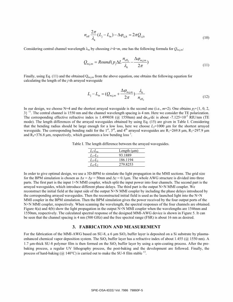
In order to give optimal design, we use a 3D-BPM to simulate the light propagation in the MMI sections. The grid size for the BPM simulation is chosen as x = y = 50nm and z = 0.1 m. The whole AWG structure is divided into three parts. The first part is the input 1×N MMI coupler, which split the input power into four channels. The second part is the arrayed waveguides, which introduce different phase delays. The third part is the output N×N MMI coupler. We reconstruct the initial field at the input side of the output N×N MMI coupler by including the phase delays introduced by the corresponding arrayed waveguides. Then the reconstructed initial field is used as the launched light into the N×N MMI coupler in the BPM simulation. Then the BPM simulation gives the power received by the four output ports of the N×N MMI coupler, respectively. When scanning the wavelength, the spectral responses of the four channels are obtained. Figure 4(a) and 4(b) show the light propagation in the output N×N MMI coupler when the wavelengths are 1546nm and 1550nm, respectively. The calculated spectral response of the designed MMI-AWG device is shown in Figure 5. It can be seen that the channel spacing is 4 nm (500 GHz) and the free spectral range (FSR) is about 16 nm as desired.
3. FABRICATION AND MEASUREMENT For the fabrication of the MMI-AWG based on SU-8, a 6 m SiO2 buffer layer is deposited on a Si substrate by plasma-enhanced chemical vapor deposition system. The SiO2 buffer layer has a refractive index of about 1.455 (@ 1550 nm). A 1.7 m-thick SU-8 polymer film is then formed on the SiO2 buffer layer by using a spin-coating process. After the pre-baking process, a regular UV lithography process, the post-baking and the development are followed. Finally, the process of hard-baking (@ 140°C) is carried out to make the SU-8 film stable 13.
SPIE-OSA-IEEE/ Vol. 7986 79860F-5
(a)
(b)
Figure 4. The BPM simulation results for the propagation of light with different wavelengths:
(a) =1546 nm; (b) =1550 nm
Figure 5. The simulated spectrum responses for all four channels of the designed MMI-AWG.
SPIE-OSA-IEEE/ Vol. 7986 79860F-6

Figure 6(a) shows the SEM view of the fabricated 4 channel MMI-AWG. Figure 7(b) and 7(c) show the SEM views of the 1×4 and 4×4 MMI couplers, which have a length of 103.8 m and 406.1 m, respectively.
In order to obtain the characterization of the fabricated MMI-AWG, a tunable laser is used as the light source. In order to improve the coupling efficiency, the input light was butt-coupled into the input waveguide through a tapered lens fiber (TLF) with a focus spot size of 2.5 m. In our measurement, the butt-coupling loss is about 8dB per facet. To measure the spectral response, the output light is collected to a power meter by using another TLF. The large coupling loss is mainly caused by the mode mismatching between the fiber and the SU-8 waveguide.
Input waveguide
1 4 MMI coupler
Array waveguide
4 4 MMI coupler
Output waveguide
(a)
103.8 m
(b)
406.1 m
(c)
Figure 6. The SEM pictures: (a) the fabricated 4-channel MMI-AWG; (b) the 1×4 MMI coupler; (c) the 4×4 MMI coupler;
SPIE-OSA-IEEE/ Vol. 7986 79860F-7

Figure 7 (a) and 7 (b) show the measured spectral responses of all the 4 channels and channel #3 of the fabricated MMI-AWG device, respectively. The channel spacing and free spectral range (FSR) is about 4 nm (500 GHz) and 16 nm respectively. Both them agree very well with the design values. The minimal excess loss is about 3.5 dB. The crosstalk between adjacent channels is about -12dB and the 3dB bandwidth is about 3.3 nm (> 80% of the channel spacing).
(a)
FSR 16nm
-3dB
-12dB
(b)Figure 7. The normalized spectral responses of the fabricated MMI-AWG. (a) all four channels; (b) channel #3.
4. CONCLUSION We have designed and fabricated a 4-channel MMI-AWG demultiplexer based on SU-8 strip waveguides. The MMI couplers are used here in order to avoid the use of a slab waveguide (i.e., free propagation region) in a regular AWG, in which there is a significant mode mismatching loss between the FPRs and the arrayed waveguides when the refractive index contrast is high. For our fabricated MMI-AWG, the measured total insertion loss is about 22 dB, which mainly comes from the coupling loss (16dB) between the input/output waveguide and the fibers. The measured channel spacing is about 4 nm (500 GHz) and the 3 dB bandwidth is about 3.3 nm (>80% of the channel spacing), which agree well with the design values. The crosstalk between adjacent channels is about –12 dB, which is close to the theoretical calculation result.
5. ACKNOWLEDGEMENT This project was partially supported by Zhejiang Provincial Natural Science Foundation (No. R1080193) and the National Nature Science Foundation of China (No. 60688401 and 61077040)
SPIE-OSA-IEEE/ Vol. 7986 79860F-8

REFERENCES
1. Bogaerts, W., Taillaert, D., Luyssaert, B., Dumon, P., Campenhout, J., Bienstman, P., Thourhout, D., Baets, R., Wiaux, V. and Beckx, S., "Basic structures for photonic integrated circuits in silicon-on-insulator," Opt. Express., 12(8), 1583-1591 (2004).
2. Tsuchizawa, T., Yamada, K., Fukuda, H., Watanabe, T., Takahashi, J. Takahashi, M., Shoji T., Tamechika, E., Itabashi S. and Morita, H., "Microphotonics Devices Based on Silicon," IEEE J. Sel. Top. Quantum Electron., 11(1), 232-240, (2005).
3. B. Yang, L. Yang, R. Hu, Z. Shen, D. Dai, Q. Liu, and S. He, “Fabrication and characterization of small optical ridge waveguides based on SU-8 polymer”, Journal Of Lightwave Technology, vol. 27, no.18, September 15, 2009, pp. 4091-4096.
4. T. C. Sum, A.A.Bettiol, J.A.vanKan, F.Watt, E.Y.B.Pun, and K.K.Tung, “Proton beam writing of low-loss polymer optical waveguides,”Appl. Phys. Lett. vol. 83, no. 9, September 2003, pp.1707–1709.
5. A. Borrenman, S. Musa, A.A.M. Kok, M.B.J. Diemeer and A. Driessen, “Fabrication of Polymeric Multimode Waveguides and Devices in SU-8 Photoresist Using Selective Polymerization”, Proccedings Symposium IEEE/LEOS Benelux Chapter, 2002, Amsterdam.
6. B.Bêche, N.Pelletier, E.Gaviot, and J.Zyss,“Single-mode TE00–TM00 optical waveguides on SU-8 polymer”, Opt.Commun., vol.230, 2004, pp.91–94.
7. Gerd E. Keiser, “ A review of WDM technology and applications”, Optical Fiber Technology, vol.5 1999, pp.3-39. 8. MeintK.Smit and Cor van Dam, “PHASAR-Based WDM-Devices principles, design and applications” Journal Of
Selected Topics In Quantum Electronics, vol.2, no.2, June 1996, pp. 236-250. 9. Daoxin Dai, Xin Fu, Yaocheng Shi, and Sailing He, “Experimental demonstration of an ultracompact Si-nanowire-
based reflective arrayed-waveguide grating (de)multiplexer with photonic crystal reflectors”, Optical Letters, vol. 35, no. 15, August 1, 2010, pp. 2594-2596.
10. Pavel Cheben, Dan-Xia Xu, Siegfried Janz, André Delâge, “Scaling down photonic waveguide devices on the SOI platform”, Proc. of SPIE, vol. 5117, pp. 147-156.
11. Mohammad R. Paiam and Robert I. MacDonald, “Design of phased-array wavelength division multiplexers using multimode interference couplers”, Applied Optics, vol.36, no.21, 20 July 1997, pp. 5097-5108.
12. Lucas B. Soldano and Erik C. M. Pennings, “Optical multi-mode interference devices based on self-imaging principles and applications”, Journal Of Lightwave Technology, vol. 13, no. 4, April 1995, pp. 615-627.
13. C. Y. Chao, and L. J. Guo, “Thermal-flow technique for reducing surface roughness and controlling gap size in polymer microring resonators”, Appl. Phys. Letts., vol.84, no.14, , April 2004, pp.2479-2481.
SPIE-OSA-IEEE/ Vol. 7986 79860F-9