Fingerprint Classification by Directional Image Partitioning
Upload
independentCategory
view
0download
0
C h a p t e r S e v e n
Power Dividers andDirectional Couplers
Power dividers and directional couplers are passive microwave components used for powerdivision or power combining, as illustrated in Figure 7.1. In power division, an input signal isdivided into two (or more) output signals of lesser power, while a power combiner acceptstwo or more input signals and combines them at an output port. The coupler or divider mayhave three ports, four ports, or more, and may be (ideally) lossless. Three-port networks takethe form of T-junctions and other power dividers, while four-port networks take the form ofdirectional couplers and hybrids. Power dividers usually provide in-phase output signals withan equal power division ratio (3 dB), but unequal power division ratios are also possible. Di-rectional couplers can be designed for arbitrary power division, while hybrid junctions usuallyhave equal power division. Hybrid junctions have either a 90◦ or a 180◦ phase shift between theoutput ports.
A wide variety of waveguide couplers and power dividers were invented and characterizedat the MIT Radiation Laboratory in the 1940s. These included E- and H -plane waveguideT-junctions, the Bethe hole coupler, multihole directional couplers, the Schwinger coupler,the waveguide magic-T, and various types of couplers using coaxial probes. In the mid-1950sthrough the 1960s, many of these couplers were reinvented to use stripline or microstrip tech-nology. The increasing use of planar lines also led to the development of new types of couplersand dividers, such as the Wilkinson divider, the branch line hybrid, and the coupled line direc-tional coupler.
We will first discuss some of the general properties of three- and four-port networks, andthen treat the analysis and design of several of the most common types of power dividers,couplers, and hybrids.
In this section we will use properties of the scattering matrix developed in Section 4.3 to de-rive some of the basic characteristics of three- and four-port networks. We will also define

Chapter 7: Power Dividers and Directional Couplers
Divideror
couplerP1
(a) (b)
P2 = �P1 P1 = P2 + P3
P3 = (1 – �)P1
Divideror
coupler
P2
P3
FIGURE 7.1 Power division and combining. (a) Power division. (b) Power combining.
isolation, coupling, and directivity, which are important quantities for the characterizationof couplers and hybrids.
The simplest type of power divider is a T-junction, which is a three-port network with twoinputs and one output. The scattering matrix of an arbitrary three-port network has nineindependent elements:
[S] =[ S11 S12 S13
S21 S22 S23S31 S32 S33
]. (7.1)
If the device is passive and contains no anisotropic materials, then it must be reciprocaland its scattering matrix will be symmetric (Si j = S ji ). Usually, to avoid power loss, wewould like to have a junction that is lossless and matched at all ports. We can easily show,however, that it is impossible to construct such a three-port lossless reciprocal network thatis matched at all ports.
If all ports are matched, then Sii = 0, and if the network is reciprocal, the scatteringmatrix of (7.1) reduces to
[S] =[ 0 S12 S13
S12 0 S23S13 S23 0
]. (7.2)
If the network is also lossless, then energy conservation requires that the scattering matrixsatisfy the unitary properties of (4.53), which leads to the following conditions [1, 2]:
|S12|2 + |S13|2 = 1, (7.3a)
|S12|2 + |S23|2 = 1, (7.3b)
|S13|2 + |S23|2 = 1, (7.3c)
S∗13S23 = 0, (7.3d)
S∗23S12 = 0, (7.3e)
S∗12S13 = 0. (7.3f)
Equations (7.3d)–(7.3f) show that at least two of the three parameters (S12, S13, S23) mustbe zero. However, this condition will always be inconsistent with one of equations (7.3a)–(7.3c), implying that a three-port network cannot be simultaneously lossless, reciprocal,and matched at all ports. If any one of these three conditions is relaxed, then a physicallyrealizable device is possible.
If the three-port network is nonreciprocal, then Si j �= S ji , and the conditions of inputmatching at all ports and energy conservation can be satisfied. Such a device is known as acirculator, and generally relies on an anisotropic material, such as ferrite, to achieve non-reciprocal behavior. Ferrite circulators will be discussed in more detail in Chapter 9, but

7.1 Basic Properties of Dividers and Douplers
we can demonstrate here that any matched lossless three-port network must be nonrecip-rocal and, thus, a circulator. The scattering matrix of a matched three-port network has thefollowing form:
[S] =[ 0 S12 S13
S21 0 S23S31 S32 0
]. (7.4)
If the network is lossless, [S] must be unitary, which implies the following conditions:
S∗31S32 = 0, (7.5a)
S∗21S23 = 0, (7.5b)
S∗12S13 = 0, (7.5c)
|S12|2 + |S13|2 = 1, (7.5d)
|S21|2 + |S23|2 = 1, (7.5e)
|S31|2 + |S32|2 = 1. (7.5f)
These equations can be satisfied in one of two ways. Either
S12 = S23 = S31 = 0, |S21| = |S32| = |S13| = 1, (7.6a)
or
S21 = S32 = S13 = 0, |S12| = |S23| = |S31| = 1. (7.6b)
These results shows that Si j �= S ji for i �= j , which implies that the device must be non-reciprocal. The scattering matrices for the two solutions of (7.6) are shown in Figure 7.2,together with the symbols for the two possible types of circulators. The only differencebetween the two cases is in the direction of power flow between the ports: solution (7.6a)corresponds to a circulator that allows power flow only from port 1 to 2, or port 2 to 3, orport 3 to 1, while solution (7.6b) corresponds to a circulator with the opposite direction ofpower flow.
Alternatively, a lossless and reciprocal three-port network can be physically realizedif only two of its ports are matched [1]. If ports1and 2 are the matched ports, then thescattering matrix can be written as
[S] =[ 0 S12 S13
S12 0 S23S13 S23 S33
]. (7.7)
12
3
12
3
0 0 11[S] = 0 00 1 0
(a)
0 1 00[S] = 0 11 0 0
(b)
FIGURE 7.2 Two types of circulators and their scattering matrices. (a) Clockwise circulation.(b) Counterclockwise circulation. The phase references for the ports are arbitrary.

Chapter 7: Power Dividers and Directional Couplers
1 2
3
[S] =0
e j�
0
e j�
00
00
e j�
S21 = e j�
S12 = e j�
S33 = e j�
FIGURE 7.3 A reciprocal lossless three-port network matched at ports 1 and 2.
To be lossless, the following unitarity conditions must be satisfied:
S∗13S23 = 0, (7.8a)
S∗12S13 + S∗
23S33 = 0, (7.8b)
S∗23S12 + S∗
33S13 = 0, (7.8c)
|S12|2 + |S13|2 = 1, (7.8d)
|S12|2 + |S23|2 = 1, (7.8e)
|S13|2 + |S23|2 + |S33|2 = 1. (7.8f)
Equations (7.8d) and (7.8e) show that |S13| = |S23|, so (7.8a) leads to the result that S13 =S23 = 0. Then, |S12| = |S33| = 1. The scattering matrix and corresponding signal flowgraph for this network are shown in Figure 7.3, where it is seen that the network actu-ally degenerates into two separate components—one a matched two-port line and the othera totally mismatched one-port.
Finally, if the three-port network is allowed to be lossy, it can be reciprocal andmatched at all ports; this is the case of the resistive divider, which will be discussed inSection 7.2. In addition, a lossy three-port network can be made to have isolation betweenits output ports (e.g., S23 = S32 = 0).
The scattering matrix of a reciprocal four-port network matched at all ports has the follow-ing form:
[S] =⎡⎢⎣
0 S12 S13 S14S12 0 S23 S24S13 S23 0 S34S14 S24 S34 0
⎤⎥⎦. (7.9)
If the network is lossless, 10 equations result from the unitarity, or energy conservation,condition [1, 2]. Consider the multiplication of row 1 and row 2, and the multiplication ofrow 4 and row 3:
S∗13S23 + S∗
14S24 = 0, (7.10a)
S∗14S13 + S∗
24S23 = 0. (7.10b)

7.1 Basic Properties of Dividers and Douplers
Multiply (7.10a) by S∗24, and (7.10b) by S∗
13, and subtract to obtain
S∗14(|S13|2 − |S24|2) = 0. (7.11)
Similarly, the multiplication of row 1 and row 3, and the multiplication of row 4 and row2, gives
S∗12S23 + S∗
14S34 = 0, (7.12a)
S∗14S12 + S∗
34S23 = 0. (7.12b)
Multiply (7.12a) by S12, and (7.12b) by S34, and subtract to obtain
S23(|S12|2 − |S34|2) = 0. (7.13)
One way for (7.11) and (7.13) to be satisfied is if S14 = S23 = 0, which results in a direc-tional coupler. Then the self-products of the rows of the unitary scattering matrix of (7.9)yield the following equations:
|S12|2 + |S13|2 = 1, (7.14a)
|S12|2 + |S24|2 = 1, (7.14b)
|S13|2 + |S34|2 = 1, (7.14c)
|S24|2 + |S34|2 = 1, (7.14d)
which imply that |S13| = |S24| [using (7.14a) and (7.14b)], and that |S12| = |S34| [using(7.14b) and (7.14d)].
Further simplification can be made by choosing the phase references on three of thefour ports. Thus, we choose S12 = S34 = α, S13 = βe jθ , and S24 = βe jφ , where α and β
are real, and θ and φ are phase constants to be determined (one of which we are still freeto choose). The dot product of rows 2 and 3 gives
S∗12S13 + S∗
24S34 = 0, (7.15)
which yields a relation between the remaining phase constants as
θ + φ = π ± 2nπ. (7.16)
If we ignore integer multiples of 2π, there are two particular choices that commonly occurin practice:
1. A Symmetric Coupler: θ = φ = π/2. The phases of the terms having amplitudeβ
are chosen equal. Then the scattering matrix has the following form:
[S] =⎡⎢⎣
0 α jβ 0α 0 0 jβjβ 0 0 α
0 jβ α 0
⎤⎥⎦. (7.17)
2. An Antisymmetric Coupler: θ = 0, φ = π . The phases of the terms having ampli-tude β are chosen to be 180◦ apart. Then the scattering matrix has the followingform:
[S] =⎡⎢⎣
0 α β 0α 0 0 −β
β 0 0 α
0 −β α 0
⎤⎥⎦. (7.18)

Chapter 7: Power Dividers and Directional Couplers
1 2
4 3
Input
Isolated
Through
Coupled
1 2
4 3
Input
Isolated
Through
Coupled
FIGURE 7.4 Two commonly used symbols for directional couplers, and power flow conventions.
Note that these two couplers differ only in the choice of reference planes. In addition,the amplitudes α and β are not independent, as (7.14a) requires that
α2 + β2 = 1. (7.19)
Thus, apart from phase references, an ideal four-port directional coupler has only one de-gree of freedom, leading to two possible configurations.
Another way for (7.11) and (7.13) to be satisfied is if |S13| = |S24| and |S12| = |S34|.If we choose phase references, however, such that S13 = S24 = α and S12 = S34 = jβ[which satisfies (7.16)], then (7.10a) yields α(S23 + S∗
14) = 0, and (7.12a) yields β(S∗14 −
S23) = 0. These two equations have two possible solutions. First, S14 = S23 = 0, which isthe same as the above solution for the directional coupler. The other solution occurs forα = β = 0, which implies that S12 = S13 = S24 = S34 = 0. This is the degenerate case oftwo decoupled two-port networks (between ports 1 and 4, and ports 2 and 3), which is oftrivial interest and will not be considered further. We are thus left with the conclusion thatany reciprocal, lossless, matched four-port network is a directional coupler.
The basic operation of a directional coupler can be illustrated with the aid of Figure 7.4,which shows two commonly used symbols for a directional coupler and the port definitions.Power supplied to port 1 is coupled to port 3 (the coupled port) with the coupling factor|S13|2 = β2, while the remainder of the input power is delivered to port 2 (the throughport) with the coefficient |S12|2 = α2 = 1 − β2. In an ideal directional coupler, no poweris delivered to port 4 (the isolated port).
The following quantities are commonly used to characterize a directional coupler:
Coupling = C = 10 logP1
P3= −20 log β dB, (7.20a)
Directivity = D = 10 logP3
P4= 20 log
β
|S14| dB, (7.20b)
Isolation = I = 10 logP1
P4= −20 log |S14| dB, (7.20c)
Insertion loss = L = 10 logP1
P2= −20 log |S12| dB. (7.20d)
The coupling factor indicates the fraction of the input power that is coupled to the out-put port. The directivity is a measure of the coupler’s ability to isolate forward and back-ward waves (or the coupled and uncoupled ports). The isolation is a measure of the power

7.1 Basic Properties of Dividers and Douplers
delivered to the uncoupled port. These quantities are related as
I = D + C dB. (7.21)
The insertion loss accounts for the input power delivered to the through port, diminished bypower delivered to the coupled and isolated ports. The ideal coupler has infinite directivityand isolation (S14 = 0). Then both α and β can be determined from the coupling factor, C .
Hybrid couplers are special cases of directional couplers, where the coupling factor is3 dB, which implies that α = β = 1/
√2. There are two types of hybrids. The quadrature
hybrid has a 90◦ phase shift between ports 2 and 3 (θ = φ = π/2) when fed at port 1, andis an example of a symmetric coupler. Its scattering matrix has the following form:
[S] = 1√2
⎡⎢⎣
0 1 j 01 0 0 jj 0 0 10 j 1 0
⎤⎥⎦. (7.22)
The magic-T hybrid and the rat-race hybrid have a 180◦ phase difference between ports2 and 3 when fed at port 4, and are examples of an antisymmetric coupler. Its scatteringmatrix has the following form:
[S] = 1√2
⎡⎢⎣
0 1 1 01 0 0 −11 0 0 10 −1 1 0
⎤⎥⎦. (7.23)
POINT OF INTEREST: Measuring Coupler Directivity
The directivity of a directional coupler is a measure of the coupler’s ability to separate forwardand reverse wave components, and applications of directional couplers often require high (35 dBor greater) directivity. Poor directivity will limit the accuracy of a reflectometer, and can causevariations in the coupled power level from a coupler when there is even a small mismatch onthe through line.
The directivity of a coupler generally cannot be measured directly because it involves alow-level signal that can be masked by coupled power from a reflected wave on the througharm. For example, if a coupler has C = 20 dB and D = 35 dB, with a load having a return lossRL = 30 dB, the signal level through the directivity path will be D + C = 55 dB below theinput power, but the reflected power through the coupled arm will only be RL + C = 50 dBbelow the input power.
One way to measure coupler directivity uses a sliding matched load, as follows. First, thecoupler is connected to a source and a matched load, as shown in the accompanying left-handfigure, and the coupled output power is measured. If we assume an input power Pi , this powerwill be Pc = C2 Pi , where C = 10(−CdB)/20 is the numerical voltage coupling factor of thecoupler. Next, the position of the coupler is reversed, and the through line is terminated with asliding load, as shown in the right-hand figure.
Vi , Pi
C
Pc
Load
Vi , Pi
CCD
V0
Slidingload
(Pmax, Pmin)
Γ
Changing the position of the sliding load introduces a variable phase shift in the signal re-flected from the load and coupled to the output port. The voltage at the output port can be

Chapter 7: Power Dividers and Directional Couplers
written as
V0 = Vi
(CD
+ C |�|e− jθ)
,
where Vi is the input voltage, D = 10(D dB)/20 ≥ 1 is the numerical value of the directivity, |�|is the reflection coefficient magnitude of the load, and θ is the path length difference betweenthe directivity and reflected signals. Moving the sliding load changes θ , so the two signals willcombine to trace out a circular locus, as shown in the following figure.
Im V0
0ReV0
Vmax
CΓVi
Vmin
V0
ViCD
�
The minimum and maximum output powers are given by
Pmin = Pi
(CD
− C |�|)2
, Pmax = Pi
(CD
+ C |�|)2
.
Let M and m be defined in terms of these powers as follows:
M = PcPmax
=(
D1 + |�|D
)2, m = Pmax
Pmin=
(1 + |�|D1 − |�|D
)2.
These ratios can be accurately measured directly by using a variable attenuator between thesource and coupler. The coupler directivity (numerical) can then be found as
D = M(
2mm + 1
).
This method requires that |�| < 1/D or, in dB, RL > D.
Reference: M. Sucher and J. Fox, eds., Handbook of Microwave Measurements, 3rd edition, Volume II, Polytech-nic Press, New York, 1963.
The T-junction power divider is a simple three-port network that can be used for powerdivision or power combining, and it can be implemented in virtually any type of transmis-sion line medium. Figure 7.5 shows some commonly used T-junctions in waveguide andmicrostrip line or stripline form. The junctions shown here are, in the absence of transmis-sion line loss, lossless junctions. Thus, as discussed in the preceding section, such junctionscannot be matched simultaneously at all ports. We will analyze the T-junction divider be-low, followed by a discussion of the resistive power divider, which can be matched at allports but is not lossless.
The lossless T-junction dividers of Figure 7.5 can all be modeled as a junction of threetransmission lines, as shown in Figure 7.6 [3]. In general, there may be fringing fields and

7.2 The T-Junction Power Divider
(a)
(c)
(b)
FIGURE 7.5 Various T-junction power dividers. (a) E-plane waveguide T. (b) H -plane wave-guide T. (c) Microstrip line T-junction divider.
higher order modes associated with the discontinuity at such a junction, leading to storedenergy that can be accounted for by a lumped susceptance, B. In order for the divider to bematched to the input line of characteristic impedance Z0, we must have
Yin = j B + 1Z1
+ 1Z2
= 1Z0
. (7.24)
If the transmission lines are assumed to be lossless (or of low loss), then the characteristicimpedances are real. If we also assume B = 0, then (7.24) reduces to
1Z1
+ 1Z2
= 1Z0
. (7.25)
In practice, if B is not negligible, some type of discontinuity compensation or a reac-tive tuning element can usually be used to cancel this susceptance, at least over a narrowfrequency range.
Yin
jBV0Z0
Z1
Z2
+
–
FIGURE 7.6 Transmission line model of a lossless T-junction divider.

Chapter 7: Power Dividers and Directional Couplers
The output line impedances, Z1 and Z2, can be selected to provide various powerdivision ratios. Thus, for a 50 � input line, a 3 dB (equal split) power divider can be madeby using two 100 � output lines. If necessary, quarter-wave transformers can be used tobring the output line impedances back to the desired levels. If the output lines are matched,then the input line will be matched. There will be no isolation between the two outputports, however, and there will be a mismatch looking into the output ports.
EXAMPLE 7.1 THE T-JUNCTION POWER DIVIDER
A lossless T-junction power divider has a source impedance of 50 �. Find the out-put characteristic impedances so that the output powers are in a 2:1 ratio. Computethe reflection coefficients seen looking into the output ports.
SolutionIf the voltage at the junction is V0, as shown in Figure 7.6, the input power to thematched divider is
Pin = 12
V 20
Z0,
while the output powers are
P1 = 12
V 20
Z1= 1
3Pin,
P2 = 12
V 20
Z2= 2
3Pin.
These results yield the characteristic impedances as
Z1 = 3Z0 = 150 �,
Z2 = 3Z0
2= 75 �.
The input impedance to the junction is
Z in = 75||150 = 50 �,
so that the input is matched to the 50 � source.Looking into the 150 � output line, we see an impedance of 50 || 75 = 30 �,
while at the 75 � output line we see an impedance of 50 || 150 = 37.5 �. Thereflection coefficients seen looking into these ports are
�1 = 30 − 15030 + 150
= −0.666,
�2 = 37.5 − 7537.5 + 75
= −0.333.■
If a three-port divider contains lossy components, it can be made to be matched at all ports,although the two output ports may not be isolated [3]. The circuit for such a divider isillustrated in Figure 7.7, using lumped-element resistors. An equal-split (−3 dB) divider isshown, but unequal power division ratios are also possible.

7.2 The T-Junction Power Divider
Zin
Port 1
Port 3
Port 2
Z0/3
V1Z0
Z0
Z0
P2
P3
P1
+
–V Z+
–
Z0/3
Z0/3
V 2+
–
V3
+–
FIGURE 7.7 An equal-split three-port resistive power divider.
The resistive divider of Figure 7.7 can easily be analyzed using circuit theory. Assum-ing that all ports are terminated in the characteristic impedance Z0, the impedance Z , seenlooking into the Z0/3 resistor followed by a terminated output line, is
Z = Z0
3+ Z0 = 4Z0
3. (7.26)
Then the input impedance of the divider is
Zin = Z0
3+ 2Z0
3= Z0, (7.27)
which shows that the input is matched to the feed line. Because the network is symmetricfrom all three ports, the output ports are also matched. Thus, S11 = S22 = S33 = 0.
If the voltage at port 1 is V1, then by voltage division the voltage V at the center of thejunction is
V = V12Z0/3
Z0/3 + 2Z0/3= 2
3V1, (7.28)
and the output voltages are, again by voltage division,
V2 =V3 = VZ0
Z0 + Z0/3= 3
4V = 1
2V1. (7.29)
Thus, S21 = S31 = S23 = 1/2, so the output powers are 6 dB below the input power level.The network is reciprocal, so the scattering matrix is symmetric, and it can be written as
[S] = 12
[ 0 1 11 0 11 1 0
]. (7.30)
The reader may verify that this is not a unitary matrix.The power delivered to the input of the divider is
Pin = 12
V 21
Z0, (7.31)

Chapter 7: Power Dividers and Directional Couplers
while the output powers are
P2 = P3 = 12
(1/2V1)2
Z0= 1
8V 2
1Z0
= 14
Pin, (7.32)
which shows that half of the supplied power is dissipated in the resistors.
The lossless T-junction divider suffers from the disadvantage of not being matched at allports, and it does not have isolation between output ports. The resistive divider can bematched at all ports, but even though it is not lossless, isolation is still not achieved. Fromthe discussion in Section 7.1, however, we know that a lossy three-port network can bemade having all ports matched, with isolation between output ports. The Wilkinson powerdivider [4] is such a network, with the useful property of appearing lossless when the outputports are matched; that is, only reflected power from the output ports is dissipated.
The Wilkinson power divider can be made with arbitrary power division, but we willfirst consider the equal-split (3 dB) case. This divider is often made in microstrip line orstripline form, as depicted in Figure 7.8a; the corresponding transmission line circuit isgiven in Figure 7.8b. We will analyze this circuit by reducing it to two simpler circuitsdriven by symmetric and antisymmetric sources at the output ports. This “even-odd” modeanalysis technique [5] will also be useful for other networks that we will study in latersections.
For simplicity, we can normalize all impedances to the characteristic impedance Z0, andredraw the circuit of Figure 7.8b with voltage generators at the output ports as shown inFigure 7.9. This network has been drawn in a form that is symmetric across the midplane;the two source resistors of normalized value 2 combine in parallel to give a resistor ofnormalized value 1, representing the impedance of a matched source. The quarter-wavelines have a normalized characteristic impedance Z , and the shunt resistor has a normalizedvalue of r ; we shall show that, for the equal-split power divider, these values should beZ = √
2 and r = 2, as given in Figure 7.8.
�/4
�/4
�4
Z0
2Z0
2Z0
Z0Z0
Z0
2Z0
Z0
2Z 0
2Z0
(a) (b)
FIGURE 7.8 The Wilkinson power divider. (a) An equal-split Wilkinson power divider in mi-crostrip line form. (b) Equivalent transmission line circuit.

7.3 The Wilkinson Power Divider
Port 3
�/4
�/4
Port 2 1
2
2
1
Vg2
Vg3
r/2
r/2
+V3
+V2
+V1
Z
Z
Port1
FIGURE 7.9 The Wilkinson power divider circuit in normalized and symmetric form.
Now define two separate modes of excitation for the circuit of Figure 7.9: the evenmode, where Vg2 = Vg3 = 2V0, and the odd mode, where Vg2 = −Vg3 = 2V0. Superpo-sition of these two modes effectively produces an excitation of Vg2 = 4V0 and Vg3 = 0,from which we can find the scattering parameters of the network. We now treat these twomodes separately.
Even mode: For even-mode excitation, Vg2 = Vg3 = 2V0, so V e2 = V e
3 , and therefore nocurrent flows through the r/2 resistors or the short circuit between the inputs of the twotransmission lines at port 1. We can then bisect the network of Figure 7.9 with open circuitsat these points to obtain the network of Figure 7.10a (the grounded side of the λ/4 line isnot shown). Then, looking into port 2, we see an impedance
Zein = Z2
2, (7.33)
FIGURE 7.10 Bisection of the circuit of Figure 7.9. (a) Even-mode excitation. (b) Odd-modeexcitation.

Chapter 7: Power Dividers and Directional Couplers
since the transmission line looks like a quarter-wave transformer. Thus, if Z = √2, port 2
will be matched for even-mode excitation; then V e2 = V0 since Ze
in = 1. The r/2 resistoris superfluous in this case since one end is open-circuited. Next, we find V e
1 from thetransmission line equations. If we let x = 0 at port 1 and x = −λ/4 at port 2, we can writethe voltage on the transmission line section as
V (x) = V +(e− jβx + �e jβx ).
Then
V e2 = V (−λ/4) = j V +(1 − �) = V0, (7.34a)
V e1 = V (0) = V +(1 + �) = j V0
� + 1� − 1
. (7.34b)
The reflection coefficient � is that seen at port 1 looking toward the resistor of normalizedvalue 2, so
� = 2 − √2
2 + √2,
and
V e1 = − j V0
√2. (7.35)
Odd mode: For odd-mode excitation, Vg2 = −Vg3 = 2V0, and so V o2 = −V o
3 , and there isa voltage null along the middle of the circuit in Figure 7.9. We can then bisect this circuitby grounding it at two points on its midplane to give the network of Figure 7.10b. Lookinginto port 2, we see an impedance of r/2 since the parallel-connected transmission line isλ/4 long and shorted at port 1, and so looks like an open circuit at port 2. Thus, port 2 willbe matched for odd-mode excitation if we select r = 2. Then V o
2 = V0 and V o1 = 0; for
this mode of excitation all power is delivered to the r/2 resistors, with none going to port 1.Finally, we must find the input impedance at port 1 of the Wilkinson divider when
ports 2 and 3 are terminated in matched loads. The resulting circuit is shown in Figure7.11a, where it is seen that this is similar to an even mode of excitation since V2 = V3.No current flows through the resistor of normalized value 2, so it can be removed, leav-ing the circuit of Figure 7.11b. We then have the parallel connection of two quarter-wavetransformers terminated in loads of unity (normalized). The input impedance is
Z in = 12(√
2)2 = 1. (7.36)
In summary, we can establish the following scattering parameters for the Wilkinsondivider:
S11 = 0 (Z in = 1 at port 1)
S22 = S33 = 0 (ports 2 and 3 matched for even and odd modes)
S12 = S21 = V e1 + V o
1V e
2 + V o2
= − j/√
2 (symmetry due to reciprocity)
S13 = S31 = − j/√
2 (symmetry of ports 2 and 3)
S23 = S32 = 0 (due to short or open at bisection)

7.3 The Wilkinson Power Divider
�/4
�/41
1
1
Port 3
Port 2
2
Zin
2
1
1
1
Port 3
Port 2
2
Zin
2
2
(a)
(b)
Port 1
Port 1
FIGURE 7.11 Analysis of the Wilkinson divider to find S11. (a) The terminated Wilkinson di-vider. (b) Bisection of the circuit in (a).
The preceding formula for S12 applies because all ports are matched when terminatedwith matched loads. Note that when the divider is driven at port 1 and the outputs arematched, no power is dissipated in the resistor. Thus the divider is lossless when the outputsare matched; only reflected power from ports 2 or 3 is dissipated in the resistor. BecauseS23 = S32 = 0, ports 2 and 3 are isolated.
EXAMPLE 7.2 DESIGN AND PERFORMANCE OF A WILKINSON DIVIDER
Design an equal-split Wilkinson power divider for a 50 � system impedance atfrequency f0, and plot the return loss (S11), insertion loss (S21 = S31), and isola-tion (S23 = S32) versus frequency from 0.5 f0 to 1.5 f0.
SolutionFrom Figure 7.8 and the above derivation, we have that the quarter-wave trans-mission lines in the divider should have a characteristic impedance of
Z = √2Z0 = 70.7 �,
and the shunt resistor a value of
R = 2Z0 = 100 �.
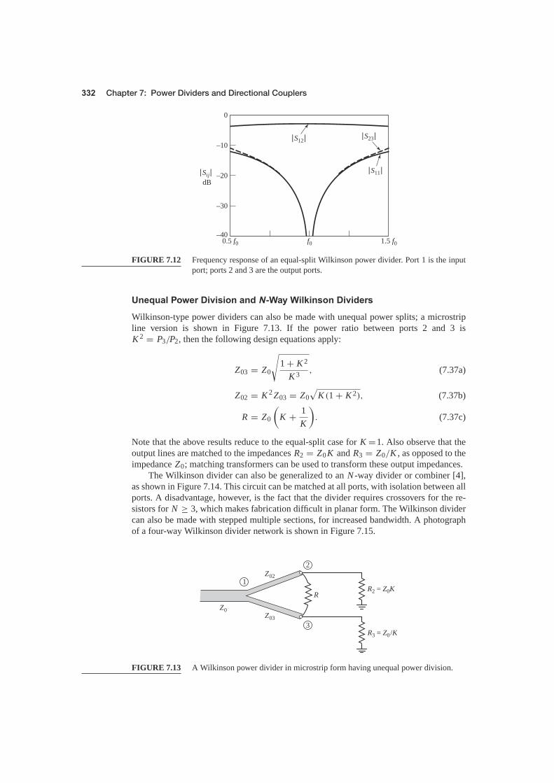
The transmission lines are λ/4 long at the frequency f0. Using a computer-aideddesign tool for the analysis of microwave circuits, the scattering parameter mag-nitudes were calculated and plotted in Figure 7.12. ■
Chapter 7: Power Dividers and Directional Couplers
0.5 f0 f0 1.5 f0–40
–30
–20⎢Sij ⎢dB
–10
0
⎢S12 ⎢
⎢S11 ⎢
⎢S23 ⎢
FIGURE 7.12 Frequency response of an equal-split Wilkinson power divider. Port 1 is the inputport; ports 2 and 3 are the output ports.
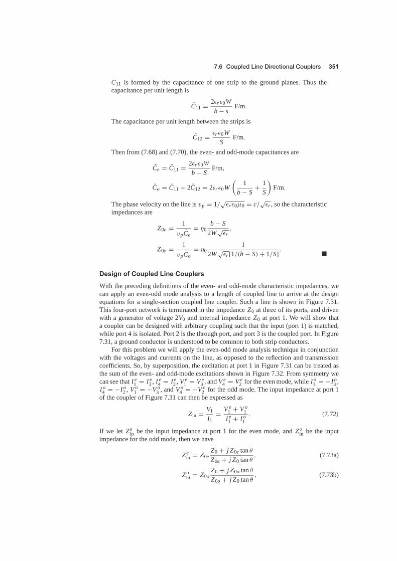
Wilkinson-type power dividers can also be made with unequal power splits; a microstripline version is shown in Figure 7.13. If the power ratio between ports 2 and 3 isK 2 = P3/P2, then the following design equations apply:
Z03 = Z0
√1 + K 2
K 3 , (7.37a)
Z02 = K 2 Z03 = Z0√
K (1 + K 2), (7.37b)
R = Z0
(K + 1
K
). (7.37c)
Note that the above results reduce to the equal-split case for K =1. Also observe that theoutput lines are matched to the impedances R2 = Z0 K and R3 = Z0/K , as opposed to theimpedance Z0; matching transformers can be used to transform these output impedances.
The Wilkinson divider can also be generalized to an N -way divider or combiner [4],as shown in Figure 7.14. This circuit can be matched at all ports, with isolation between allports. A disadvantage, however, is the fact that the divider requires crossovers for the re-sistors for N ≥ 3, which makes fabrication difficult in planar form. The Wilkinson dividercan also be made with stepped multiple sections, for increased bandwidth. A photographof a four-way Wilkinson divider network is shown in Figure 7.15.
1
2
3
Z0Z03
Z02
R2 = Z0K
R3 = Z0/K
R
FIGURE 7.13 A Wilkinson power divider in microstrip form having unequal power division.

7.4 Waveguide Directional Couplers
�/4
Z0 N
Z0 N
Z0 NZ0
Z0
Z0
Z0
Z0Z0
Z0
Z0
Z0
Z0 N
.
.
.
FIGURE 7.14 An N -way, equal-split Wilkinson power divider.
We now turn our attention to directional couplers, which are four-port devices with thecharacteristics discussed in Section 7.1. To review the basic operation, consider the direc-tional coupler schematic symbols shown in Figure 7.4. Power incident at port 1 will coupleto port 2 (the through port) and to port 3 (the coupled port), but not to port 4 (the isolatedport). Similarly, power incident in port 2 will couple to ports 1 and 4, but not 3. Thus,ports 1 and 4 are decoupled, as are ports 2 and 3. The fraction of power coupled from port1 to port 3 is given by C , the coupling coefficient, as defined in (7.20a), and the leakageof power from port 1 to port 4 is given by I , the isolation, as defined in (7.20c). Anotherquantity that characterizes a coupler is the directivity, D = I − C (dB), which is the ratio
FIGURE 7.15 Photograph of a four-way corporate power divider network using three microstripWilkinson power dividers. Note the isolation chip resistors.Courtesy of M. D. Abouzahra, MIT Lincoln Laboratory, Lexington, Mass.

Chapter 7: Power Dividers and Directional Couplers
of the powers delivered to the coupled port and the isolated port. The ideal coupler is char-acterized solely by the coupling factor, as the isolation and directivity are infinite. The idealcoupler is also lossless and matched at all ports.
Directional couplers can be made in many different forms. We will first discuss wave-guide couplers, followed by hybrid junctions. A hybrid junction is a special case of adirectional coupler, where the coupling factor is 3 dB (equal split), and the phase relationbetween the output ports is either 90◦ (quadrature hybrid), or 180◦ (magic-T or rat-racehybrid). Then we will discuss the implementation of directional couplers in coupled trans-mission line form.
The directional property of all directional couplers is produced through the use of two sep-arate waves or wave components, which add in phase at the coupled port and are canceledat the isolated port. One of the simplest ways of doing this is to couple one waveguideto another through a single small hole in the common broad wall between the two wave-guides. Such a coupler is known as a Bethe hole coupler, two versions of which are shownin Figure 7.16. From the small-aperture coupling theory of Section 4.8, we know that anaperture can be replaced with equivalent sources consisting of electric and magnetic dipolemoments [6]. The normal electric dipole moment and the axial magnetic dipole momentradiate with even symmetry in the coupled guide, while the transverse magnetic dipole mo-ment radiates with odd symmetry. Thus, by adjusting the relative amplitudes of these twoequivalent sources, we can cancel the radiation in the direction of the isolated port, whileenhancing the radiation in the direction of the coupled port. Figure 7.16 shows two ways inwhich these wave amplitudes can be controlled; in the coupler shown in Figure 7.16a, the
a3
4
2
(Isolated)
(Through)
1(Input)
3(Coupled)
2(Through)
4 (Isolated)
1S b
b
yx
z
(Coupled)
(Input)
(a)
(b)
�
FIGURE 7.16 Two versions of the Bethe hole directional coupler. (a) Parallel waveguides.(b) Skewed waveguides.

7.4 Waveguide Directional Couplers
two waveguides are parallel and the coupling is controlled by s, the aperture offset fromthe sidewall of the waveguide. For the coupler of Figure 7.16b, the wave amplitudes arecontrolled by the angle, θ , between the two waveguides.
First consider the configuration of Figure 7.16a, with an incident TE10 mode intoport 1. These fields can be written as
Ey = A sinπxa
e− jβz, (7.38a)
Hx = −AZ10
sinπxa
e− jβz, (7.38b)
Hz = jπ AβaZ10
cosπxa
e− jβz, (7.38c)
where Z10 = k0η0/β is the wave impedance of the TE10 mode. Then, from (4.124) and(4.125), this incident wave generates the following equivalent polarization currents at theaperture at x = s, y = b, z = 0:
Pe = ε0αe y A sinπsa
δ(x − s)δ(y − b)δ(z), (7.39a)
Pm = −αm A[ −x
Z10sin
πsa
+ zjπ
βaZ10cos
πsa
]δ(x − s)δ(y − b)δ(z). (7.39b)
Using (4.128a) and (4.128b) to relate Pe and Pm to the currents J and M , and then using(4.118), (4.120), (4.122), and (4.123), gives the amplitudes of the forward and reversetraveling waves in the top guide as
A+10 = −1
P10
∫v
E−10 · J dv + 1
P10
∫v
H−10 · Mdv
= − jωAP10
[ε0αe sin2 πs
a− μ0αm
Z210
(sin2 πs
a+ π2
β2a2 cos2 πsa
)], (7.40a)
A−10 = −1
P10
∫v
E+10 · J dv + 1
P10
∫v
H+10 · Mdv
= − jωAP10
[ε0αe sin2 πs
a+ μ0αm
Z210
(sin2 πs
a− π2
β2a2 cos2 πsa
)], (7.40b)
where P10 = ab/Z10 is the power normalization constant. Note from (7.40a) and (7.40b)that the amplitude of the wave excited toward port 4 (A+
10) is generally different from thatexcited toward port 3 (A−
10) (because H+x = −H−
x ), so we can cancel the power deliveredto port 4 by setting A+
10 = 0. If we assume that the aperture is round, then Table 4.3 givesthe polarizabilities as αe = 2r3
0/3 and αm = 4r30/3, where r0 is the radius of the aperture.
Then from (7.40a) we obtain the following condition for A+10 = 0:(
2ε0 − 4μ0
Z210
)sin2 πs
a− 4π2μ0
β2a2 Z210
cos2 πsa
= 0,
(k2
0 − 2β2) sin2 πsa
= 2π2
a2 cos2 πsa
,(4π2
a2 − k20
)sin2 πs
a= 2π2
a2 ,

Chapter 7: Power Dividers and Directional Couplers
or
sinπsa
= π
√2
4π2 − k20a2
= λ0√2(λ2
0 − a2) . (7.41)
The coupling factor is then given by
C = 20 log∣∣∣∣ A
A−10
∣∣∣∣ dB (7.42a)
and the directivity by
D = 20 log∣∣∣∣ A−
10A+
10
∣∣∣∣ dB. (7.42b)
Thus, a Bethe hole coupler of the type shown in Figure 7.16a can be designed by firstusing (7.41) to find s, the position of the aperture, and then using (7.42a) to determine theaperture size, r0, to give the required coupling factor.
For the skewed geometry of Figure 7.16b, the aperture may be centered at s = a/2,and the skew angle θ adjusted for cancellation at port 4. In this case, the normal electricfield does not change with θ , but the transverse magnetic field components are reduced bycos θ . We can account for the skew angle by replacing αm in the previous derivation byαm cos θ . The wave amplitudes of (7.40a) and (7.40b) then become, for s = a/2,
A+10 = − jωA
P10
(ε0αe − μ0αm
Z210
cos θ
), (7.43a)
A−10 = − jωA
P10
(ε0αe + μ0αm
Z210
cos θ
). (7.43b)
Setting A+10 = 0 results in the following condition for the angle θ :
2ε0 − 4μ0
Z210
cos θ = 0,
or
cos θ = k20
2β2 . (7.44)
The coupling factor then simplifies to
C = 20 log∣∣∣∣ A
A−10
∣∣∣∣ = −20 log4k2
0r30
3abβdB. (7.45)
The angular geometry of the skewed Bethe hole coupler is often a disadvantage interms of fabrication and application. In addition, both coupler designs operate properlyonly at the design frequency; deviation from this frequency will alter the coupling leveland the directivity, as shown in the following example.
EXAMPLE 7.3 BETHE HOLE COUPLER DESIGN AND PERFORMANCE
Design a Bethe hole coupler of the type shown in Figure 7.16a for an X-bandwaveguide operating at 9 GHz, with a coupling of 20 dB. Calculate and plot thecoupling and directivity from 7 to 11 GHz. Assume a round aperture.

7.4 Waveguide Directional Couplers
SolutionFor an X-band waveguide at 9 GHz, we have the following constants:
a = 0.02286 m,
b = 0.01016 m,
λ0 = 0.0333 m,
k0 = 188.5 m−1,
β = 129.0 m−1,
Z10 = 550.9 �,
P10 = 4.22 × 10⁻⁷ m2/�.
Equation (7.41) can be used to find the aperture position s:
sinπsa
= λ0√2(λ2
0 − a2) = 0.972,
s = aπ
sin−1 0.972 = 0.424a = 9.69 mm.
The coupling is 20 dB, so
C = 20 dB = 20 log
∣∣∣∣∣ AA−
10
∣∣∣∣∣,or ∣∣∣∣∣ A
A−10
∣∣∣∣∣ = 1020/20 = 10;
thus, |A−10/A| = 1/10. Now use (7.40b) to find r0:∣∣∣∣∣ A−10A
∣∣∣∣∣ = 110
= ω
P10
[(ε0αe + μ0αm
Z210
)(0.944) − π2μ0αm
β2a2 Z210
(0.056)
].
Because αe = 2r30/3 and αm = 4r3
0/3, we obtain
0.1 = 1.44 × 10⁶r30 ,
or
r0 = 4.15 mm.
This completes the design of the Bethe hole coupler. To compute the couplingand directivity versus frequency, we evaluate (7.42a) and (7.42b), using the ex-pressions for A−
10 and A+10 given in (7.40a) and (7.40b). In these expressions the
aperture position and size are fixed at s = 9.69 mm and r0 = 4.15 mm, and thefrequency is varied. A short computer program was used to calculate the datashown in Figure 7.17. Observe that the coupling varies by less than 1 dB over theband. The directivity is very large (>60 dB) at the design frequency but decreasesto 15–20 dB at the band edges. The directivity is a more sensitive function offrequency because it depends on the cancellation of two wave components. ■

Chapter 7: Power Dividers and Directional Couplers
7.0 7.5 8.0 8.5 9.0Frequency GHz
9.5 10.0 10.5 11.060
50
40
30
C, D
dB
20
10
0
C
D
FIGURE 7.17 Coupling and directivity versus frequency for the Bethe hole coupler of Exam-ple 7.3.
As seen from Example 7.3, a single-hole coupler has a relatively narrow bandwidth, atleast in terms of its directivity. However, if the coupler is designed with a series of couplingholes, the extra degrees of freedom can be used to increase this bandwidth. The principleof operation and design of such a multihole waveguide coupler is very similar to that of themultisection matching transformer.
First let us consider the operation of the two-hole coupler shown in Figure 7.18. Twoparallel waveguides sharing a common broad wall are shown, although the same type ofstructure could be made in microstrip line or stripline form. Two small apertures are spacedλg/4 apart and couple the two guides. A wave entering at port 1 is mostly transmittedthrough to port 2, but some power is coupled through the two apertures. If a phase referenceis taken at the first aperture, then the phase of the wave incident at the second aperture willbe −90◦. Each aperture will radiate a forward wave component and a backward wavecomponent into the upper guide; in general, the forward and backward amplitudes aredifferent. In the direction of port 3, both wave components are in phase because both havetraveled λg/4 to the second aperture. However, we obtain a cancellation in the direction ofport 4 because the wave coming through the second aperture travels λg/2 further than thewave component coming through the first aperture. Clearly, this cancellation is frequencysensitive, making the directivity a sensitive function of frequency. The coupling is lessfrequency dependent since the path lengths from port 1 to port 3 are always the same.
4 3
1 2
�g /4
0° –90°
(Isolated)
(Out of phase) (In phase)
(Input)
(Coupled)
(Through)
FIGURE 7.18 Basic operation of a two-hole directional coupler.

7.4 Waveguide Directional Couplers
d
B0A
B F
A A
F0A
n = 0
B1A F1A
n = 1
B2A F2A
n = 2
B3A F3A
. . .
BNA FN A
n = N
FIGURE 7.19 Geometry of an (N + 1)-hole waveguide directional coupler.
Thus, in the multihole coupler design, we synthesize the directivity response, as opposedto the coupling response, as a function of frequency.
Now consider the general case of the multihole coupler shown in Figure 7.19, whereN + 1 equally spaced apertures couple two parallel waveguides. The amplitude of the inci-dent wave in the lower left guide is A and, for small coupling, is essentially the same as theamplitude of the through wave. For instance, a 20 dB coupler has a power coupling factorof 10−20/10 = 0.01, so the power transmitted through waveguide A is 1 − 0.01 = 0.99 ofthe incident power (1% coupled to the upper guide). The voltage (or field) drop in wave-guide A is
√0.99 = 0.995, or 0.5%. Thus, the assumption that the amplitude of the incident
field is identical at each aperture is a good one. Of course, the phase will change from oneaperture to the next.
As we saw in the previous section for the Bethe hole coupler, an aperture generallyexcites forward and backward traveling waves with different amplitudes. Thus, let
Fn denote the coupling coefficient of the nth aperture in the forward direction.Bn denote the coupling coefficient of the nth aperture in the backward direction.
Then the amplitude of the forward wave can be written as
F = Ae− jβNdN∑
n=0Fn, (7.46)
since all components travel the same path length. The amplitude of the backward wave is
B = AN∑
n=0Bne−2 jβnd , (7.47)
since the path length for the nth component is 2βnd, where d is the spacing between theapertures. In (7.46) and (7.47) the phase reference is taken at the n = 0 aperture.
From the definitions in (7.20a) and (7.20b) the coupling and directivity can be com-puted as
C = −20 log∣∣∣∣ F
A
∣∣∣∣ = −20 log∣∣∣∣ N∑
n=0Fn
∣∣∣∣ dB, (7.48)
D = −20 log∣∣∣∣ B
F
∣∣∣∣ = −20 log
∣∣∣∣∣∑N
n=0 Bne−2 jβnd∑Nn=0 Fn
∣∣∣∣∣= −C − 20 log
∣∣∣∣ N∑n=0
Bne−2 jβnd∣∣∣∣ dB. (7.49)

Chapter 7: Power Dividers and Directional Couplers
Now assume that the apertures are round holes with identical positions s relative tothe edge of the guide, with rn being the radius of the nth aperture. Then we know fromSection 4.8 and the preceding section that the coupling coefficients will be proportionalto the polarizabilities αe and αm of the aperture, and hence proportional to r3
n . So we canwrite
Fn = Kf r3n , (7.50a)
Bn = Kbr3n , (7.50b)
where Kf and Kb are constants for the forward and backward coupling coefficients that arethe same for all apertures, but are functions of frequency. Then (7.48) and (7.49) reduce to
C = −20 log |Kf | − 20 logN∑
n=0r3
n dB, (7.51)
D = −C − 20 log |Kb| − 20 log
∣∣∣∣∣N∑
n=0r3
n e−2 jβnd
∣∣∣∣∣= −C − 20 log |Kb| − 20 log S dB. (7.52)
In (7.51), the second term is constant with frequency. The first term is not affectedby the choice of rn, but is a relatively slowly varying function of frequency. Similarly,in (7.52) the first two terms are slowly varying functions of frequency, representing thedirectivity of a single aperture, but the last term (S) is a sensitive function of frequency dueto phase cancellation in the summation. Thus we can choose the rn to synthesize a desiredfrequency response for the directivity, while the coupling should be relatively constant withfrequency.
Observe that the last term in (7.52),
S =∣∣∣∣∣
N∑n=0
r3n e−2 jβnd
∣∣∣∣∣, (7.53)
is very similar in form to the expression obtained in Section 5.5 for multisection quarter-wave matching transformers. As in that case, we can develop coupler designs that yieldeither a binomial (maximally flat) or a Chebyshev (equal ripple) response for the directivity.Another interpretation of (7.53) may be recognizable to the student familiar with basicantenna theory, as this expression is identical to the array pattern factor of an (N + 1)-element array with element weights r3
n . In that case, too, the pattern may be synthesized interms of binomial or Chebyshev polynomials.
Binomial response: As in the case of the multisection quarter-wave matching transformers,we can obtain a binomial, or maximally flat, response for the directivity of the multiholecoupler by making the coupling coefficients proportional to the binomial coefficients. Thus,
r3n = kC N
n , (7.54)
where k is a constant to be determined, and C Nn is a binomial coefficient given in (5.51).
To find k, we evaluate the coupling using (7.51) to give
C = −20 log |Kf | − 20 log k − 20 logN∑
n=0C N
n dB. (7.55)

7.4 Waveguide Directional Couplers
Because we know Kf, N , and C , we can solve for k and then find the required apertureradii from (7.54). The spacing, d , should be λg/4 at the center frequency.
Chebyshev response: First assume that N is even (an odd number of holes), and that thecoupler is symmetric, so that r0 = rN , r1 = rN−1, etc. Then from (7.53) we can write S as
S =∣∣∣∣∣
N∑n=0
r3n e−2 jnθ
∣∣∣∣∣ = 2N/2∑n=0
r3n cos(N − 2n)θ,
where θ = βd . To achieve a Chebyshev response we equate this to the Chebyshev polyno-mial of degree N :
S = 2N/2∑n=0
r3n cos(N − 2n)θ = k|TN (sec θm cos θ)|, (7.56)
where k and θm are constants to be determined. From (7.53) and (7.56), we see that forθ = 0, S = ∑N
n=0 r3n = k|TN (sec θm)|. Using this result in (7.51) gives the coupling as
C = −20 log |Kf | − 20 log S∣∣θ=0
= −20 log |Kf | − 20 log k − 20 log |TN (sec θm)| dB. (7.57)
From (7.52) the directivity is
D = −C − 20 log |Kb| − 20 log S
= 20 logKf
Kb+ 20 log
TN (sec θm)
TN (sec θm cos θ)dB. (7.58)
The term log Kf/Kb is a function of frequency, so D will not have an exact Chebyshevresponse. This error is usually small, however. We can assume that the smallest value ofD will occur when TN (sec θm cos θ) = 1, since |TN (sec θm)| ≥ |TN (sec θm cos θ)|. So ifDmin is the specified minimum value of directivity in the passband, then θm can be foundfrom the relation
Dmin = 20 log TN (sec θm) dB. (7.59)
Alternatively, we could specify the bandwidth, which then dictates θm and Dmin. In eithercase, (7.57) can then be used to find k, and then (7.56) solved for the radii, rn .
If N is odd (an even number of holes), the results for C, D, and Dmin in (7.57), (7.58),and (7.59) still apply, but instead of (7.56), the following relation is used to find the apertureradii:
S = 2(N−1)/2∑
n=0r3
n cos(N − 2n)θ = k|TN (sec θm cos θ)|. (7.60)
EXAMPLE 7.4 MULTIHOLE WAVEGUIDE COUPLER DESIGN
Design a four-hole Chebyshev coupler in an X-band waveguide using round aper-tures located at s = a/4. The center frequency is 9 GHz, the coupling is 20 dB,and the minimum directivity is 40 dB. Plot the coupling and directivity responsefrom 7 to 11 GHz.

Chapter 7: Power Dividers and Directional Couplers
SolutionFor an X-band waveguide at 9 GHz, we have the following constants:
a = 0.02286 m,
b = 0.01016 m,
λ0 = 0.0333 m,
k0 = 188.5 m−1,
β = 129.0 m−1,
Z10 = 550.9 �,
P10 = 4.22 × 10⁻⁷ m2/�.
From (7.40a) and (7.40b), we obtain for an aperture at s = a/4:
|Kf | = 2k0
3η0 P10
[sin2 πs
a− 2β2
k20
(sin2 πs
a+ π2
β2a2 cos2 πsa
)]= 3.953 ×10⁵,
|Kb| = 2k0
3η0 P10
[sin2 πs
a+ 2β2
k20
(sin2 πs
a− π2
β2a2 cos2 πsa
)]= 3.454 ×10⁵.
For a four-hole coupler, N = 3, so (7.59) gives
40 = 20 log T3(sec θm) dB,
100 = T3(sec θm) = cosh[3 cosh−1(sec θm)
],
sec θm = 3.01,
where (5.58b) was used. Thus θm = 70.6◦ and 109.4◦ at the band edges. Thenfrom (7.57) we can solve for k:
C = 20 = −20 log(3.953 × 10⁵) − 20 log k − 40 dB,
20 log k = −171.94,
k = 2.53 × 10⁻⁹.
Finally, (7.60) and the expansion from (5.60c) for T3 allow us to solve for the radiias follows:
S = 2(r3
0 cos 3θ + r31 cos θ
) = k[
sec3 θm(cos 3θ + 3 cos θ) − 3 sec θm cos θ],
2r30 = k sec3 θm ⇒ r0 = r3 = 3.26 mm,
2r31 = 3k(sec3 θm − sec θm) ⇒ r1 = r2 = 4.51 mm.
The resulting coupling and directivity are plotted in Figure 7.20; note the in-creased directivity bandwidth compared to that of the Bethe hole coupler ofExample 7.3. ■

7.5 The Quadrature (90◦) Hybrid
7.0 7.5 8.0
C
D
8.5 9.0Frequency GHz
9.5 10.0 10.5 11.060
50
40
30
C, D
dB
20
10
0
FIGURE 7.20 Coupling and directivity versus frequency for the four-hole coupler of Exam-ple 7.4.
◦
Quadrature hybrids are 3 dB directional couplers with a 90◦ phase difference in the out-puts of the through and coupled arms. This type of hybrid is often made in microstrip lineor stripline form as shown in Figure 7.21 and is also known as a branch-line hybrid. Other3 dB couplers, such as coupled line couplers or Lange couplers, can also be used as quadra-ture couplers; these components will be discussed in later sections. Here we will analyzethe operation of the quadrature hybrid using an even-odd mode decomposition techniquesimilar to that used for the Wilkinson power divider.
With reference to Figure 7.21, the basic operation of the branch-line coupler is asfollows. With all ports matched, power entering port 1 is evenly divided between ports 2and 3, with a 90◦ phase shift between these outputs. No power is coupled to port 4 (theisolated port). The scattering matrix has the following form:
[S] = −1√2
⎡⎢⎣
0 j 1 0j 0 0 11 0 0 j0 1 j 0
⎤⎥⎦. (7.61)
Observe that the branch-line hybrid has a high degree of symmetry, as any port can be usedas the input port. The output ports will always be on the opposite side of the junction fromthe input port, and the isolated port will be the remaining port on the same side as the inputport. This symmetry is reflected in the scattering matrix, as each row can be obtained as atransposition of the first row.
�4
Z0
Z0 Z0
Z0/ 2
Z0/ 2
Z0
Z0 Z0
�4
1
4
(Input)
(Isolated)
(Output)
(Output)
2
3
FIGURE 7.21 Geometry of a branch-line coupler.

Chapter 7: Power Dividers and Directional Couplers
4 3
1 2A1 = 1
B3B4
B1 B2
1
1 1
1
11 1
1
1
1/ 2
1/ 2
FIGURE 7.22 Circuit of the branch-line hybrid coupler in normalized form.
We first draw the schematic circuit of the branch-line coupler in normalized form, as inFigure 7.22, where it is understood that each line represents a transmission line with in-dicated characteristic impedance normalized to Z0. The common ground return for eachtransmission line is not shown. We assume that a wave of unit amplitude A1 = 1 is incidentat port 1.
The circuit of Figure 7.22 can be decomposed into the superposition of an even-modeexcitation and an odd-mode excitation [5], as shown in Figure 7.23. Note that superimpos-ing the two sets of excitations produces the original excitation of Figure 7.22, and since thecircuit is linear, the actual response (the scattered waves) can be obtained from the sum ofthe responses to the even and odd excitations.
Because of the symmetry or antisymmetry of the excitation, the four-port network canbe decomposed into a set of two decoupled two-port networks, as shown in Figure 7.23.Because the amplitudes of the incident waves for these two-ports are ±1/2, the amplitudes
1 2
4 3
+1/2
+1/21 1
1
1 1 1
11
1/ 2
1/ 2
Line of symmetryI = 0V = max
+1/2
+1/2
Te
1 1
1
1
1
1
1
1
1/ 2
1/ 2
Open-circuited stubs(2 separate 2-ports)
Γe
1 2
4 3
–1/2
+1/21 1
1
1 1 1
11
1/ 2
1/ 2
Line of antisymmetryV = 0I = max
–1/2
+1/2
To
1 1
1
1
1
1
1
1
11
1/ 2
1/ 2
Short-circuited stubs(2 separate 2-ports)
Γo
(a)
(b)
FIGURE 7.23 Decomposition of the branch-line coupler into even- and odd-mode excitations.(a) Even mode (e). (b) Odd mode (o).

7.5 The Quadrature (90◦) Hybrid
of the emerging wave at each port of the branch-line hybrid can be expressed as
B1 = 12�e + 1
2�o, (7.62a)
B2 = 12
Te + 12
To, (7.62b)
B3 = 12
Te − 12
To, (7.62c)
B4 = 12�e − 1
2�o, (7.62d)
where �e,o and Te,o are the even- and odd-mode reflection and transmission coefficientsfor the two-port networks of Figure 7.23. First consider the calculation of �e and Te forthe even-mode two-port circuit. This can best be done by multiplying the ABCD matricesof each cascade component in that circuit, to give
[A BC D
]e
=[
1 0j 1
]︸ ︷︷ ︸
ShuntY = j
[0 j/
√2
j√
2 0
]︸ ︷︷ ︸
λ/4Transmission
line
[1 0j 1
]︸ ︷︷ ︸
ShuntY = J
= 1√2
[−1 jj −1
],
(7.63)
where the individual matrices can be found from Table 4.1, and the admittance of the shuntopen-circuited λ/8 stubs is Y = j tan β� = j . Then Table 4.2 can be used to convert fromABCD parameters (defined here with Zo = 1) to S parameters, which are equivalent to thereflection and transmission coefficients. Thus,
�e = A + B − C − DA + B + C + D
= (−1 + j − j + 1)/√
2(−1 + j + j − 1)/
√2
= 0, (7.64a)
Te = 2A + B + C + D
= 2(−1 + j + j − 1)/
√2
= −1√2(1 + j). (7.64b)
Similarly, for the odd mode we obtain[A BC D
]o
= 1√2
[1 jj 1
], (7.65)
which gives the reflection and transmission coefficients as
�o = 0, (7.66a)
To = 1√2(1 − j). (7.66b)
Using (7.64) and (7.66) in (7.62) gives the following results:
B1 = 0 (port 1 is matched), (7.67a)
B2 = − j√2
(half-power,−90◦ phase shift from port 1 to 2), (7.67b)
B3 = − 1√2
(half-power,−180◦ phase shift from port 1 to 3), (7.67c)
B4 = 0 (no power to port 4). (7.67d)
These results agree with the first row and column of the scattering matrix given in(7.61); the remaining elements can easily be found by transposition.

Chapter 7: Power Dividers and Directional Couplers
FIGURE 7.24 Photograph of an eight-way microstrip power divider for an array antenna feed net-work at 1.26 GHz. The circuit uses six quadrature hybrids in a Bailey configurationfor unequal power division ratios (see Problem 7.33).Courtesy of ProSensing, Inc., Amherst, Mass.
In practice, due to the quarter-wave length requirement, the bandwidth of a branch-linehybrid is limited to 10%–20%. However, as with multisection matching transformers andmultihole directional couplers, the bandwidth of a branch-line hybrid can be increased toa decade or more by using multiple sections in cascade. In addition, the basic design canbe modified for unequal power division and/or different characteristic impedances at theoutput ports. Another practical point to be aware of is the fact that discontinuity effects atthe junctions of the branch-line coupler may require that the shunt arms be lengthened by10◦–20◦. Figure 7.24 shows a photograph of a circuit using several quadrature hybrids.
EXAMPLE 7.5 DESIGN AND PERFORMANCE OF A QUADRATURE HYBRID
Design a 50 � branch-line quadrature hybrid junction, and plot the scatteringparameter magnitudes from 0.5 f0 to 1.5 f0, where f0 is the design frequency.
SolutionAfter the preceding analysis, the design of a quadrature hybrid is trivial. The linesare λ/4 at the design frequency f0, and the branch-line impedances are
Z0√2
= 50√2
= 35.4 �.
The calculated frequency response is plotted in Figure 7.25. Note that we obtainperfect 3 dB power division at ports 2 and 3, and perfect isolation and return lossat ports 4 and 1, respectively, at the design frequency f0. All of these quantities,however, degrade quickly as the frequency departs from f0. ■
0.5 f0 f0 1.5 f0–40
–30
–20⎪Sij⎪
–10
0S13
S14
S12S11
FIGURE 7.25 Scattering parameter magnitudes versus frequency for the branch-line coupler ofExample 7.5.

7.6 Coupled Line Directional Couplers
bW S
(a)
W�r
d
W
(c)
�r
WS
bW
S
(b)
�r
FIGURE 7.26 Various coupled transmission line geometries. (a) Coupled stripline (planar, oredge-coupled). (b) Coupled stripline (stacked, or broadside-coupled). (c) Coupledmicrostrip lines.
When two unshielded transmission lines are in close proximity, power can be coupled fromone line to the other due to the interaction of the electromagnetic fields. Such lines are re-ferred to as coupled transmission lines, and they usually consist of three conductors in closeproximity, although more conductors can be used. Figure 7.26 shows several examples ofcoupled transmission lines. Coupled transmission lines are sometimes assumed to operatein the TEM mode, which is rigorously valid for coaxial line and stripline structures, butonly approximately valid for microstrip line, coplanar waveguide, or slotline structures.Coupled transmission lines can support two distinct propagating modes, and this featurecan be used to implement a variety of practical directional couplers, hybrids, and filters.
The coupled lines shown in Figure 7.26 are symmetric, meaning that the two conduct-ing strips have the same width and position relative to ground; this simplifies the analysisof their operation. We will first discuss the basic theory of coupled lines and present somedesign data for coupled stripline and coupled microstrip line. We will then analyze theoperation of a single-section coupled line directional coupler and extend these results tomultisection coupled line coupler design.
The coupled lines of Figure 7.26, or other symmetric three-wire lines, can be representedby the structure and equivalent circuit shown in Figure 7.27. If we assume TEM prop-agation, then the electrical characteristics of the coupled lines can be completely deter-mined from the effective capacitances between the lines and the velocity of propagationon the line. As depicted in Figure 7.27, C12 represents the capacitance between the twostrip conductors, and C11 and C22 represent the capacitance between one strip conductor
C11 C22
C12
FIGURE 7.27 A three-wire coupled transmission line and its equivalent capacitance network.

Chapter 7: Power Dividers and Directional Couplers
C11 C22
C11 C22
2C12 2C12
FIGURE 7.28 Even- and odd-mode excitations for a coupled line, and the resulting equivalentcapacitance networks. (a) Even-mode excitation. (b) Odd-mode excitation.
and ground. Because the strip conductors are identical in size and location relative to theground conductor, we have C11 = C22. Note that the designation of “ground” for the thirdconductor has no special relevance beyond the fact that it is convenient, since in manyapplications this conductor is the ground plane of a stripline or microstrip circuit.
Now consider two special types of excitations for the coupled line: the even mode,where the currents in the strip conductors are equal in amplitude and in the same direction,and the odd mode, where the currents in the strip conductors are equal in amplitude but inopposite directions. The electric field lines for these two cases are sketched in Figure 7.28.Because the line is TEM, the propagation constant and phase velocity are the same forboth of these modes: β = ω/vp and vp = c/√εr , where εr is the relative permittivity ofthe TEM line.
For the even mode, the electric field has even symmetry about the center line, and nocurrent flows between the two strip conductors. This leads to the equivalent circuit shown,where C12 is effectively open-circuited. The resulting capacitance of either line to groundfor the even mode is
Ce = C11 = C22, (7.68)
assuming that the two strip conductors are identical in size and location. Then the charac-teristic impedance for the even mode is
Z0e =√
Le
Ce=
√LeCe
Ce= 1
vpCe, (7.69)
where vp = c/√εr = 1/√
LeCe = 1/√
LoCo is the phase velocity of propagation on theline.
For the odd mode, the electric field lines have an odd symmetry about the center line,and a voltage null exists between the two strip conductors. We can imagine this as a ground

7.6 Coupled Line Directional Couplers
plane through the middle of C12, which leads to the equivalent circuit shown. In this casethe effective capacitance between either strip conductor and ground is
Co = C11 + 2C12 = C22 + 2C12, (7.70)
and the characteristic impedance for the odd mode is
Z0o =√
Lo
Co=
√LoCo
Co= 1
vpCo. (7.71)
In words, Z0e (Z0o) is the characteristic impedance of one of the strip conductors relative toground when the coupled line is operated in the even (odd) mode. An arbitrary excitationof a coupled line can always be treated as a superposition of appropriate amplitudes ofeven- and odd-mode excitations. This analysis assumes the lines are symmetric, and thatfringing capacitances are identical for even and odd modes.
If the coupled line supports a pure TEM mode, such as coaxial line, parallel plateguide, or stripline, analytical techniques such as conformal mapping [7] can be used toevaluate the capacitances per unit length of line, and the even- and odd-mode character-istic impedances can then be determined. For quasi-TEM lines, such as microstrip line,these results can be obtained numerically or by approximate quasi-static techniques [8]. Ineither case, such calculations are generally too involved for our consideration, but manycommercial microwave CAD packages can provide design data for a variety of coupledlines. Here we will present only graphical design data for two cases of coupled lines.
For a symmetric coupled stripline of the type shown in Figure 7.26a, the design graphin Figure 7.29 can be used to determine the necessary strip widths and spacing for a givenset of characteristic impedances, Z0e and Z0o, and the dielectric constant. This graph
20 40 60 80 100�r Z0o
120 140 16020
40
60
80
100
120
140
160
180
200
220
� rZ 0
e
0.01 0.050.1
0.2
0.51.00.2
0.3
0.4
0.6
0.81.0
1.52.0
S/b
W/b
W
S
W
b�r
FIGURE 7.29 Normalized even- and odd-mode characteristic impedance design data for sym-metric edge-coupled striplines.

Chapter 7: Power Dividers and Directional Couplers
20 40 60 80Z0o
Z 0e
100 120
20
40
60
80
100
120
140
160
180 0.050.1
0.2
0.40.6
1.02.00.07
0.1
0.150.2
0.30.4
0.50.7
1.0
1.52.0
S/d
W/d
W Wd
S �r = 10
FIGURE 7.30 Even- and odd-mode characteristic impedance design data for symmetric coupledmicrostrip lines on a substrate with εr = 10.
should cover ranges of parameters for most practical applications, and can be used forany dielectric constant, since the TEM mode of stripline allows scaling by the dielectricconstant.
For coupled microstrip lines, the results do not scale with dielectric constant, so designgraphs must be made for specific values of dielectric constant. Figure 7.30 shows such adesign graph for symmetric coupled microstrip lines on a substrate with εr = 10. Anotherdifficulty with coupled microstrip lines is the fact that the phase velocity is usually differentfor the two modes of propagation because the two modes operate with different field con-figurations in the vicinity of the air–dielectric interface. This can have a degrading effecton coupler directivity.
EXAMPLE 7.6 IMPEDANCE OF A SIMPLE COUPLED LINE
For the broadside coupled stripline geometry of Figure 7.26b, assume W � Sand W � b, so that fringing fields can be ignored, and determine the even- andodd-mode characteristic impedances.
SolutionWe first find the equivalent network capacitances, C11 and C12 (because the lineis symmetric, C22 = C11). The capacitance per unit length of broadside parallellines with width W and separation d is
C = εWd
F/m,
where ε is the substrate permittivity. This formula ignores fringing fields.
7.6 Coupled Line Directional Couplers
C11 is formed by the capacitance of one strip to the ground planes. Thus thecapacitance per unit length is
C11 = 2εrε0Wb − s
F/m.
The capacitance per unit length between the strips is
C12 = εrε0WS
F/m.
Then from (7.68) and (7.70), the even- and odd-mode capacitances are
Ce = C11 = 2εrε0Wb − S
F/m,
Co = C11 + 2C12 = 2εrε0W(
1b − S
+ 1S
)F/m.
The phase velocity on the line is vp = 1/√
εrε0μ0 = c/√εr , so the characteristicimpedances are
Z0e = 1vpCe
= η0b − S
2W√εr
,
Z0o = 1vpCo
= η01
2W√εr [1/(b − S) + 1/S] . ■
With the preceding definitions of the even- and odd-mode characteristic impedances, wecan apply an even-odd mode analysis to a length of coupled line to arrive at the designequations for a single-section coupled line coupler. Such a line is shown in Figure 7.31.This four-port network is terminated in the impedance Z0 at three of its ports, and drivenwith a generator of voltage 2V0 and internal impedance Z0 at port 1. We will show thata coupler can be designed with arbitrary coupling such that the input (port 1) is matched,while port 4 is isolated. Port 2 is the through port, and port 3 is the coupled port. In Figure7.31, a ground conductor is understood to be common to both strip conductors.
For this problem we will apply the even-odd mode analysis technique in conjunctionwith the voltages and currents on the line, as opposed to the reflection and transmissioncoefficients. So, by superposition, the excitation at port 1 in Figure 7.31 can be treated asthe sum of the even- and odd-mode excitations shown in Figure 7.32. From symmetry wecan see that I e
1 = I e3 , I e
4 = I e2 , V e
1 = V e3 , and V e
4 = V e2 for the even mode, while I o
1 = −I o3 ,
I o4 = −I o
2 , V o1 = −V o
3 , and V o4 = −V o
2 for the odd mode. The input impedance at port 1of the coupler of Figure 7.31 can then be expressed as
Z in = V1
I1= V e
1 + V o1
I e1 + I o
1. (7.72)
If we let Zein be the input impedance at port 1 for the even mode, and Zo
in be the inputimpedance for the odd mode, then we have
Zein = Z0e
Z0 + j Z0e tan θ
Z0e + j Z0 tan θ, (7.73a)
Zoin = Z0o
Z0 + j Z0o tan θ
Z0o + j Z0 tan θ, (7.73b)

Chapter 7: Power Dividers and Directional Couplers
1
3 4
2
Coupled Isolated
ThroughInput(a)
(b)
�
Z0e, Z0o
I3Z0 Z0
+V3 +V4
I4
I1Z0 Z0
+V1 +V2
I2
2V0
1 2
43
FIGURE 7.31 A single-section coupled line coupler. (a) Geometry and port designations. (b) Theschematic circuit.
FIGURE 7.32 Decomposition of the coupled line coupler circuit of Figure 7.31 into even- andodd-mode excitations. (a) Even mode. (b) Odd mode.

7.6 Coupled Line Directional Couplers
since, for each mode, the line looks like a transmission line of characteristic impedanceZ0e or Z0o, terminated in a load impedance, Z0. Then by voltage division,
V o1 = V0
Zoin
Zoin + Z0
, (7.74a)
V e1 = V0
Zein
Zein + Z0
, (7.74b)
and
I o1 = V0
Zoin + Z0
, (7.75a)
I e1 = V0
Zein + Z0
. (7.75b)
Using these results in (7.72) yields
Zin = Zoin(Ze
in + Z0) + Ze
in(Zo
in + Z0)
Zein + Zo
in + 2Z0= Z0 + 2
(Zo
in Zein − Z2
0)
Zein + Zo
in + 2Z0. (7.76)
Now if we let
Z0 = √Z0e Z0o, (7.77)
then (7.73a) and (7.73b) reduce to
Zein = Z0e
√Z0o + j
√Z0e tan θ√
Z0e + j√
Z0o tan θ,
Zoin = Z0o
√Z0e + j
√Z0o tan θ√
Z0o + j√
Z0e tan θ,
so that Zein Zo
in = Z0e Z0o = Z20, and (7.76) reduces to
Z in = Z0. (7.78)
Thus, as long as (7.77) is satisfied, port 1 (and, by symmetry, all other ports) will bematched.
Now if (7.77) is satisfied, so that Zin = Z0, we have that V1 = V0, by voltage division.The voltage at port 3 is
V3 = V e3 + V o
3 = V e1 − V o
1 = V0
[ Zein
Zein + Z0
− Zoin
Zoin + Z0
], (7.79)
where (7.74) has been used. From (7.73) and (7.77), we can show that
Zein
Zein + Z0
= Z0 + j Z0e tan θ
2Z0 + j (Z0e + Z0o) tan θ,
Zoin
Zoin + Z0
= Z0 + j Z0o tan θ
2Z0 + j (Z0e + Z0o) tan θ,
so that (7.79) reduces to
V3 = V0j (Z0e − Z0o) tan θ
2Z0 + j (Z0e + Z0o) tan θ. (7.80)

Chapter 7: Power Dividers and Directional Couplers
Now define the coupling coefficient, C , as
C = Z0e − Z0o
Z0e + Z0o, (7.81)
which we will soon see is actually the midband voltage coupling coefficient, V3/V0. Then,√1 − C2 = 2Z0
Z0e + Z0o,
so that
V3 = V0jC tan θ√
1 − C2 + j tan θ. (7.82)
Similarly, we can show that
V4 = V e4 + V o
4 = V e2 − V o
2 = 0, (7.83)
V2 = V e2 + V o
2 = V0
√1 − C2
√1 − C2 cos θ + j sin θ
. (7.84)
Equations (7.82) and (7.84) can be used to plot the coupled and through port voltagesversus frequency, as shown in Figure 7.33. At very low frequencies (θ π/2), virtuallyall power is transmitted through port 2, with none being coupled to port 3. For θ = π/2, thecoupling to port 3 is at its first maximum; this is where the coupler is generally operated,for small size and minimum line loss. Otherwise, the response is periodic, with maxima inV3 for θ = π/2, 3π/2, . . .
For θ = π/2, the coupler is λ/4 long, and (7.82) and (7.84) reduce to
V3
V0= C, (7.85)
V2
V0= − j
√1 − C2, (7.86)
which shows that C < 1 is the voltage coupling factor at the design frequency, θ = π/2.Note that these results satisfy power conservation since Pin = (1/2)|V0|2/Z0, while theoutput powers are P2 =(1/2)|V2|2/Z0 =(1/2)(1−C2)|V0|2/Z0, P3 =(1/2)|C |2|V0|2/Z0,and P4 = 0,so that Pin = P2 + P3 + P4. Also observe that there is a 90◦ phase shift be-tween the two output port voltages; thus this coupler can be used as a quadrature hybrid.In addition, as long as (7.77) is satisfied, the coupler will be matched at the input and haveperfect isolation, at any frequency.
�0 �2
� 3� 2�0
1
1 – C2
C2
2
V2 2
V0
V3 2
V0
FIGURE 7.33 Coupled and through port voltages (squared) versus frequency for the coupled linecoupler of Figure 7.31.
7.6 Coupled Line Directional Couplers
Finally, if the characteristic impedance, Z0, and the voltage coupling coefficient, C ,are specified, then the following design equations for the required even- and odd-modecharacteristic impedances can be easily derived from (7.77) and (7.81):
Z0e = Z0
√1 + C1 − C
, (7.87a)
Z0o = Z0
√1 − C1 + C
. (7.87b)
In the above analysis it was assumed that the even and odd modes of the coupled linestructure have the same velocities of propagation, so that the line has the same electricallength for both modes. For coupled microstrip lines, or other non-TEM lines, this conditionwill generally not be satisfied exactly, and the coupler will have poor directivity. The factthat coupled microstrip lines have unequal even- and odd-mode phase velocities can beintuitively explained by considering the field line plots of Figure 7.28, which show that theeven mode has less fringing field in the air region than the odd mode. Thus its effectivedielectric constant should be higher, indicating a smaller phase velocity for the even mode.Techniques for compensating coupled microstrip lines to achieve equal even- and odd-mode phase velocities include the use of dielectric overlays and anisotropic substrates.
This type of coupler is best suited for weak coupling, as a large coupling factor requireslines that are too close together to be practical, or a combination of even- and odd-modecharacteristic impedances that is nonrealizable.
EXAMPLE 7.7 SINGLE-SECTION COUPLER DESIGN AND PERFORMANCE
Design a 20 dB single-section coupled line coupler in stripline with a groundplane spacing of 0.32 cm, a dielectric constant of 2.2, a characteristic impedanceof 50 �, and a center frequency of 3 GHz. Plot the coupling and directivity from1 to 5 GHz. Include the effect of losses by assuming a loss tangent of 0.05 for thedielectric material and copper conductors of 2 mil thickness.
SolutionThe voltage coupling factor is C = 10−20/20 = 0.1. From (7.87), the even- andodd-mode characteristic impedances are
Z0e = Z0
√1 + C1 − C
= 55.28 �,
Z0o = Z0
√1 − C1 + C
= 45.23 �.
To use Figure 7.29, we have that√
εr Z0e = 82.0,√
εr Z0o = 67.1,
and so W/b = 0.809 and S/b = 0.306. This gives a conductor width of W =0.259 cm and a conductor separation of S = 0.098 cm (these values were actuallyfound using a commercial microwave CAD package).
Figure 7.34 shows the resulting coupling and directivity versus frequency,including the effect of dielectric and conductor losses. Losses have the effectof reducing the directivity, which is typically greater than 70 dB in the absenceof loss. ■

Chapter 7: Power Dividers and Directional Couplers
1.0 2.0 3.0Frequency (GHz)
4.0 5.0
40
50
60
30
20
10
0
Cou
plin
g, D
irect
ivity
(dB
)D
C
FIGURE 7.34 Coupling versus frequency for the single-section coupler of Example 7.7.
As Figure 7.33 shows, the coupling of a single-section coupled line coupler is limited inbandwidth due to the λ/4 length requirement. As in the case of matching transformers andwaveguide couplers, bandwidth can be increased by using multiple sections. In fact, thereis a very close relationship between multisection coupled line couplers and multisectionquarter-wave transformers [9].
Because the phase characteristics are usually better, multisection coupled line couplersare generally made with an odd number of sections, as shown in Figure 7.35. Thus, we willassume that N is odd. We will also assume that the coupling is weak (C ≥ 10 dB), and thateach section is λ/4 long (θ = π/2) at the center frequency.
For a single coupled line section, with C 1, (7.82) and (7.84) simplify toV3
V1= jC tan θ√
1 − C2 + j tan θ jC tan θ
1 + j tan θ= jC sin θe− jθ , (7.88a)
V2
V1=
√1 − C2
√1 − C2 cos θ + j sin θ
e− jθ . (7.88b)
Then for θ = π/2 we have that V3/V1 = C and V2/V1 = − j . The above approximationis equivalent to assuming that no power is lost on the through path from one section tothe next, and is similar to the approximation used for the multisection waveguide coupleranalysis. It is a good assumption for small C , even though power conservation is violated.
V3 V4
V1 V2
C1 C2 CN – 1 CN
Coupled Isolated
Input Through
� �� �
. . .
FIGURE 7.35 An N -section coupled line coupler.

7.6 Coupled Line Directional Couplers
Using these results, we can express the total voltage at the coupled port (port 3) of thecascaded coupler in Figure 7.35 as
V3 = (jC1 sin θe− jθ )V1 + (
jC2 sin θe− jθ )V1e−2 jθ
+ · · · + (jCN sin θe− jθ )V1e−2 j (N−1)θ, (7.89)
where Cn is the voltage coupling coefficient of the nth section. If we assume that thecoupler is symmetric, so that C1 = CN , C2 = CN−1, etc., we can simplify (7.89) to
V3 = j V1 sin θe− jθ[C1
(1+e−2 j (N−1)θ
)+ C2(e−2 jθ + e−2 j (N−2)θ
) + · · · + CM e− j (N−1)θ]
=2 j V1sin θe− j Nθ
[C1 cos(N − 1)θ + C2 cos(N − 3)θ + · · · + 1
2CM
], (7.90)
where M = (N + 1)/2.At the center frequency, we define the voltage coupling factor C0:
C0 =∣∣∣∣V3
V1
∣∣∣∣θ=π/2
. (7.91)
Equation (7.90) is in the form of a Fourier series for the coupling as a function of fre-quency. Thus, we can synthesize a desired coupling response by choosing the coupling co-efficients, Cn . Note that in this case we synthesize the coupling response, while in the caseof the multihole waveguide coupler we synthesized the directivity response. This is becausethe path for the uncoupled arm of the multisection coupled line coupler is in the forwarddirection, and so is less dependent on frequency than the coupled arm path, which is in thereverse direction; this is the opposite situation from the multihole waveguide coupler.
Multisection couplers of this form can achieve decade bandwidths, but coupling lev-els must be low. Because of the longer electrical length, it is more critical to have equaleven- and odd-mode phase velocities than it is for the single-section coupler. This usuallymeans that stripline is the preferred medium for such couplers. Mismatched phase veloci-ties will degrade the coupler directivity, as will junction discontinuities, load mismatches,and fabrication tolerances. A photograph of a coupled line coupler is shown in Figure 7.36.
FIGURE 7.36 Photograph of a single-section microstrip coupled line coupler.Courtesy of M. D. Abouzahra, MIT Lincoln Laboratory, Lexington, Mass.

Chapter 7: Power Dividers and Directional Couplers
EXAMPLE 7.8 MULTISECTION COUPLER DESIGN AND PERFORMANCE
Design a three-section 20 dB coupled line coupler with a binomial (maximallyflat) response, a system impedance of 50 �, and a center frequency of 3 GHz.Plot the coupling and directivity from 1 to 5 GHz.
SolutionFor a maximally flat response for a three-section (N = 3) coupler, we require that
dn
dθn C(θ)
∣∣∣∣θ=π/2
= 0 for n = 1, 2.
From (7.90),
C =∣∣∣∣V3
V1
∣∣∣∣ = 2 sin θ
(C1 cos 2θ + 1
2C2
)= C1(sin 3θ − sin θ) + C2 sin θ
= C1 sin 3θ + (C2 − C1) sin θ,
so
dCdθ
= [3C1 cos 3θ + (C2 − C1) cos θ ]∣∣∣π/2
= 0,
d2Cdθ2 = [−9C1 sin 3θ − (C2 − C1) sin θ ]
∣∣∣π/2
= 10C1 − C2 = 0.
At midband, θ = π/2 and C0 = 20 dB. Thus, C = 10−20/20 = 0.1 = C2 − 2C1.Solving these two equations for C1 and C2 gives
C1 = C3 = 0.0125,
C2 = 0.125.
From (7.87) the even- and odd-mode characteristic impedances for each sectionare
Z10e = Z3
0e = 50√
1.01250.9875
= 50.63 �,
Z10o = Z3
0o = 50√
0.98751.0125
= 49.38 �,
Z20e = 50
√1.1250.875
= 56.69 �,
Z20o = 50
√0.8751.125
= 44.10 �.
The coupling and directivity for this coupler are plotted in Figure 7.37. ■

7.7 The Lange Coupler
1 2 3Frequency (GHz)
4 540
30
20
10
0
Cou
plin
g (d
B)
D > 100 dB
FIGURE 7.37 Coupling versus frequency for the three-section binomial coupler of Example 7.8.
Generally the coupling in a coupled line coupler is too loose to achieve coupling factors of3 or 6 dB. One way to increase the coupling between edge-coupled lines is to use severallines parallel to each other, so that the fringing fields at both edges of a line contribute to thecoupling. One of the most practical implementations of this idea is the Lange coupler [10],shown in Figure 7.38a, where four parallel coupled lines are used with interconnections toprovide tight coupling. This coupler can easily achieve 3 dB coupling ratios, with an octaveor more bandwidth. The design tends to compensate for unequal even- and odd-mode phasevelocities, which also improves the bandwidth. There is a 90◦ phase difference between theoutput lines (ports 2 and 3), so the Lange coupler is a type of quadrature hybrid. The maindisadvantage of the Lange coupler is probably practical, as the lines are very narrow andclose together, and the required bonding wires across the lines increases complexity. Thistype of coupled line geometry is also referred to as interdigitated; such structures can alsobe used for filter circuits.
The unfolded Lange coupler [11], shown in Figure 7.38b, operates in essentially thesame way as the original Lange coupler but is easier to model with an equivalent circuit.Such an equivalent circuit consists of a four-wire coupled line structure, as shown in Fig-ure 7.39a. All of the lines have the same width and spacing. If we make the reasonableassumption that each line couples only to its nearest neighbor, and ignore more-distantcouplings, then we effectively have a two-wire coupled line circuit, as shown in Figure7.39b. Then, if we can derive the even- and odd-mode characteristic impedances, Ze4 andZo4, of the four-wire circuit of Figure 7.39a in terms of Z0e and Z0o, the even- and odd-mode characteristic impedances of any adjacent pair of lines, we can apply the coupledline coupler results of Section 7.6 to analyze the Lange coupler.
Figure 7.40a shows the effective capacitances between the conductors of the four-wirecoupled line of Figure 7.39a. Unlike the two-line case of Section 7.6, the capacitances ofthe four lines to ground are different depending on whether the line is on the outside (1 and4), or on the inside (2 and 3). An approximate relation between these capacitances is [12]
Cin = Cex − CexCm
Cex + Cm. (7.92)

Chapter 7: Power Dividers and Directional Couplers
4
1
W
Isolated
Input
2
3
Coupled
Through
Z0
S
Z0 Z0
Z0
�/4
2
Through
Input
4
1 3
Coupled
Isolated
(a)
(b)
FIGURE 7.38 The Lange coupler. (a) Layout in microstrip form. (b) The unfolded Lange coupler.
For an even-mode excitation, all four conductors in Figure 7.40a are at the same po-tential, so Cm , has no effect, and the total capacitance of any line to ground is
Ce4 = Cex + Cin. (7.93a)
For an odd-mode excitation, electric walls effectively exist through the middle of each Cm,so the capacitance of any line to ground is
Co4 = Cex + Cin + 6Cm. (7.93b)
The even- and odd-mode characteristic impedances are then
Ze4 = 1vpCe4
, (7.94a)
Zo4 = 1vpCo4
, (7.94b)
where vp is the phase velocity of propagation on the line.Now consider any isolated pair of adjacent conductors in the four-line model; the
effective capacitances are as shown in Figure 7.40b. The even- and odd-mode capacitances

7.7 The Lange Coupler
3
1
4
2
90°
(a)
(b)
90°
Coupled Isolated
Input Through
Input Through
3 4
1 2
Coupled Isolated
Ze4, Zo4
Ze4, Zo4
FIGURE 7.39 Equivalent circuits for the unfolded Lange coupler. (a) Four-wire coupled linemodel. (b) Approximate two-wire coupled line model.
are
Ce = Cex, (7.95a)
Co = Cex + 2Cm . (7.95b)
Solving (7.95) for Cex and Cm , and substituting into (7.93) with the aid of (7.92) gives theeven-odd mode capacitances of the four-wire line in terms of a two-wire coupled line:
Ce4 = Ce(3Ce + Co)
Ce + Co, (7.96a)
Co4 = Co(3Co + Ce)
Ce + Co. (7.96b)
Because characteristic impedances are related to capacitance as Z0 = 1/vpC , we canrewrite (7.96) to give the even/odd mode characteristic impedances of the Lange coupler interms of the characteristic impedances of a two-conductor line that is identical to any pair
1 2 3 4Cm
Cex Cin Cin Cex
Cm Cm
(a)
1 2
CexCex
Cm
(b)
FIGURE 7.40 Effective capacitance networks for the unfolded Lange coupler equivalent cir-cuits of Figure 7.39. (a) Effective capacitance network for the four-wire model.(b) Effective capacitance network for the two-wire model.

Chapter 7: Power Dividers and Directional Couplers
of adjacent lines in the coupler:
Ze4 = Z0o + Z0e
3Z0o + Z0eZ0e, (7.97a)
Zo4 = Z0o + Z0e
3Z0e + Z0oZ0o, (7.97b)
where Z0e and Z0o are the even- and odd-mode characteristic impedances of the two-conductor pair.
Now we can apply the results of Section 7.6 to the coupler of Figure 7.39b. From(7.77) the characteristic impedance is
Z0 = √Ze4 Zo4 =
√Z0e Z0o(Z0o + Z0e)2
(3Z0o + Z0e)(3Z0e + Z0o), (7.98)
and the voltage coupling coefficient is, from (7.81),
C = Ze4 − Zo4
Ze4 + Zo4= 3
(Z2
0e − Z20o)
3(Z2
0e + Z20o) + 2Z0e Z0o
, (7.99)
where (7.97) was used. For design purposes it is useful to invert these results to give thenecessary even- and odd-mode impedances in terms of a desired characteristic impedanceand coupling coefficient:
Z0e = 4C − 3 + √9 − 8C2
2C√
(1 − C)/(1 + C)Z0, (7.100a)
Z0o = 4C + 3 − √9 − 8C2
2C√
(1 + C)/(1 − C)Z0. (7.100b)
These results are approximate because of the simplifications involved with the appli-cation of two-line characteristic impedances to the four-line circuit, and because of theassumption of equal even- and odd-mode phase velocities. In practice, however, these re-sults generally give sufficient accuracy. If necessary, a more complete analysis can be madeto directly determine Ze4 and Zo4 for the four-line circuit, as in reference [13].
◦
The 180◦ hybrid junction is a four-port network with a 180◦ phase shift between the twooutput ports. It can also be operated so that the outputs are in phase. With reference to the180◦ hybrid symbol shown in Figure 7.41, a signal applied to port 1 will be evenly splitinto two in-phase components at ports 2 and 3, and port 4 will be isolated. If the input isapplied to port 4, it will be equally split into two components with a 180◦ phase differenceat ports 2 and 3, and port 1 will be isolated. When operated as a combiner, with inputsignals applied at ports 2 and 3, the sum of the inputs will be formed at port 1, while the
1
4
2
3
180°hybrid
(Σ)
(Δ)
FIGURE 7.41 Symbol for a 180◦ hybrid junction.
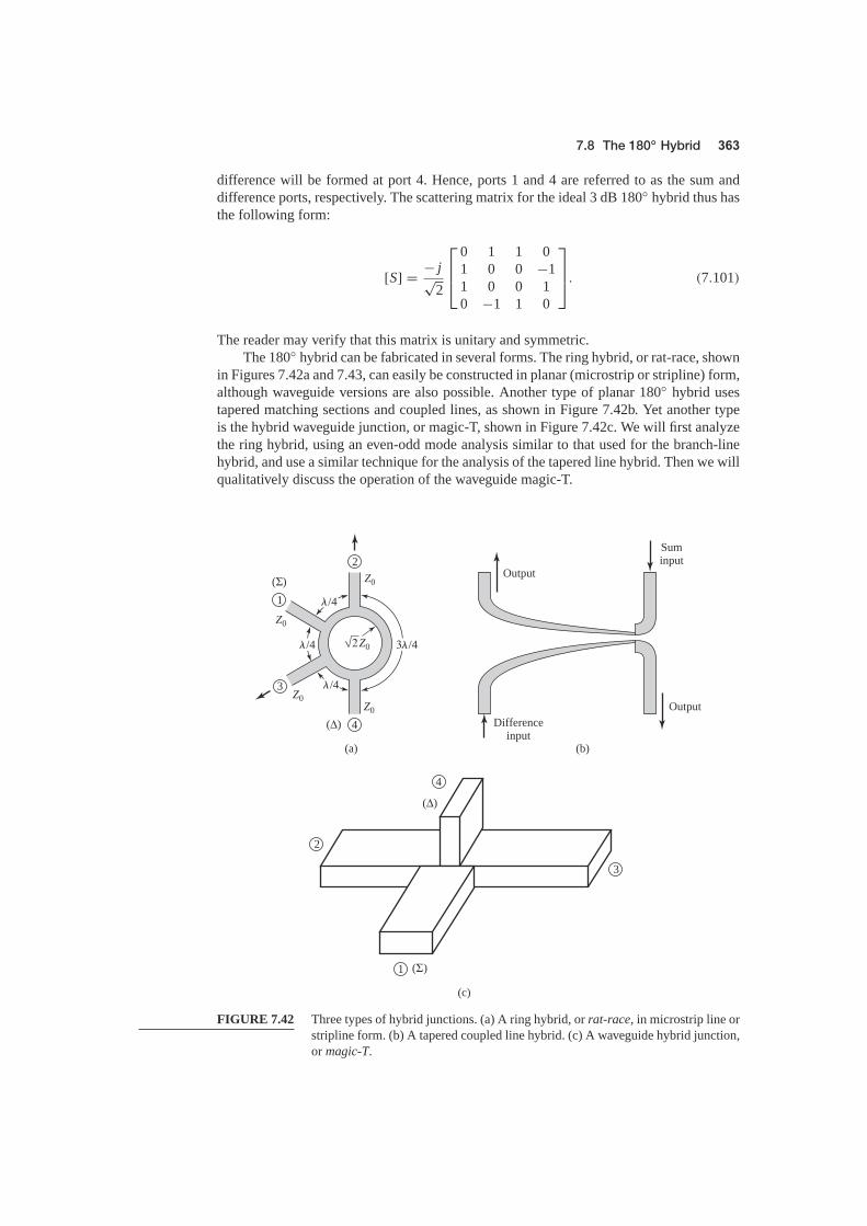
7.8 The 180◦ Hybrid
difference will be formed at port 4. Hence, ports 1 and 4 are referred to as the sum anddifference ports, respectively. The scattering matrix for the ideal 3 dB 180◦ hybrid thus hasthe following form:
[S] = − j√2
⎡⎢⎣
0 1 1 01 0 0 −11 0 0 10 −1 1 0
⎤⎥⎦. (7.101)
The reader may verify that this matrix is unitary and symmetric.The 180◦ hybrid can be fabricated in several forms. The ring hybrid, or rat-race, shown
in Figures 7.42a and 7.43, can easily be constructed in planar (microstrip or stripline) form,although waveguide versions are also possible. Another type of planar 180◦ hybrid usestapered matching sections and coupled lines, as shown in Figure 7.42b. Yet another typeis the hybrid waveguide junction, or magic-T, shown in Figure 7.42c. We will first analyzethe ring hybrid, using an even-odd mode analysis similar to that used for the branch-linehybrid, and use a similar technique for the analysis of the tapered line hybrid. Then we willqualitatively discuss the operation of the waveguide magic-T.
2
4
4
2
1
3
3
1 �/4
�/4
�/4
3�/42Z0
(Σ)
(Δ)Z0
Z0
Z0
Z0
(a) (b)
(c)
Output
Suminput
OutputDifference
input
(Σ)
(Δ)
FIGURE 7.42 Three types of hybrid junctions. (a) A ring hybrid, or rat-race, in microstrip line orstripline form. (b) A tapered coupled line hybrid. (c) A waveguide hybrid junction,or magic-T.

Chapter 7: Power Dividers and Directional Couplers
FIGURE 7.43 Photograph of a microstrip power divider network using three ring hybrids.Courtesy of M. D. Abouzahra, MIT Lincoln Laboratory, Lexington, Mass.
First consider a unit amplitude wave incident at port 1 (the sum port) of the ring hybrid ofFigure 7.42a. At the ring junction this wave will divide into two components, which botharrive in phase at ports 2 and 3, and 180◦ out of phase at port 4. Using the even-odd modeanalysis technique [5], we can decompose this case into a superposition of the two simplercircuits and excitations shown in Figure 7.44. The amplitudes of the scattered waves from
4
1 22
1
3
+1/2
+1/21
1
O.C.
O.C.
O.C.
�/4
�/83�/8
+1/2
22
2
Te
Γe
(a)
4
1 22
1
3
+1/2
–1/21
1
S.C.
S.C.
S.C.
�/4
�/83�/8
+1/2
22
2
To
Γo
(b)
FIGURE 7.44 Even- and odd-mode decomposition of the ring hybrid when port 1 is excited witha unit amplitude incident wave. (a) Even mode. (b) Odd mode.

7.8 The 180◦ Hybrid
the ring hybrid will be
B1 = 12�e + 1
2�o, (7.102a)
B2 = 12
Te + 12
To, (7.102b)
B3 = 12�e − 1
2�o, (7.102c)
B4 = 12
Te − 12
To. (7.102d)
We can evaluate the required reflection and transmission coefficients defined in Figure 7.44using the ABCD matrix for the even- and odd-mode two-port circuits in Figure 7.44. Theresults are [
A BC D
]e
=[
1 j√
2j√
2 −1
], (7.103a)
[A BC D
]o
=[ −1 j
√2
j√
2 1
]. (7.103b)
Then with the aid of Table 4.2 we have
�e = − j√2, (7.104a)
Te = − j√2, (7.104b)
�o = j√2, (7.104c)
To = − j√2. (7.104d)
Using these results in (7.102) gives
B1 = 0, (7.105a)
B2 = − j√2, (7.105b)
B3 = − j√2, (7.105c)
B4 = 0, (7.105d)
which shows that the input port is matched, port 4 is isolated, and the input power is evenlydivided and in phase between ports 2 and 3. These results form the first row and column ofthe scattering matrix in (7.101).
Next consider a unit amplitude wave incident at port 4 (the difference port) of thering hybrid of Figure 7.42a. The two wave components on the ring will arrive in phase atport 2 and at port 3, with a relative phase difference of 180◦ between these two ports. Thetwo wave components will be 180◦ out of phase at port 1. This case can be decomposedinto a superposition of the two simpler circuits and excitations shown in Figure 7.45. The

Chapter 7: Power Dividers and Directional Couplers
4
3
1 22
1O.C.
O.C.
O.C.
�/4
�/83�/8
22
2Γe
(a)
1
1
+1/2
+1/2
Te
4
3
1 22
1S.C.
S.C.
S.C.
�/4
�/83�/8
22
2Γo
(b)
1
1
–1/2
–1/2
+1/2
+1/2
To
FIGURE 7.45 Even- and odd-mode decomposition of the ring hybrid when port 4 is excited witha unit amplitude incident wave. (a) Even mode. (b) Odd mode.
amplitudes of the scattered waves will be
B1 = 12
Te − 12
To, (7.106a)
B2 = 12�e − 1
2�o, (7.106b)
B3 = 12
Te + 12
To, (7.106c)
B4 = 12�e + 1
2�o. (7.106d)
The ABCD matrices for the even- and odd-mode circuits of Figure 7.45 are[A BC D
]e
=[ −1 j
√2
j√
2 1
], (7.107a)[
A BC D
]o
=[
1 j√
2j√
2 −1
]. (7.107b)
Then, from Table 4.2, the necessary reflection and transmission coefficients are
�e = j√2, (7.108a)
Te = − j√2, (7.108b)
�o = − j√2, (7.108c)
To = − j√2. (7.108d)

7.8 The 180◦ Hybrid
Using these results in (7.106) givesB1 = 0, (7.109a)
B2 = j√2, (7.109b)
B3 = − j√2, (7.109c)
B4 = 0, (7.109d)
which shows that the input port is matched, port 1 is isolated, and the input power is evenlydivided into ports 2 and 3 with a 180◦ phase difference. These results form the fourth rowand column of the scattering matrix of (7.101). The remaining elements in this matrix canbe found from symmetry considerations.
The bandwidth of the ring hybrid is limited by the frequency dependence of the ringlengths, but is generally on the order of 20%–30%. Increased bandwidth can be obtainedby using additional sections, or a symmetric ring circuit as suggested in reference [14].
EXAMPLE 7.9 DESIGN AND PERFORMANCE OF A RING HYBRID
Design a 180◦ ring hybrid for a 50 � system impedance, and plot the magnitudeof the scattering parameters (S1 j ) from 0.5 f0 to 1.5 f0, where f0 is the designfrequency.
SolutionWith reference to Figure 7.42a, the characteristic impedance of the ring transmis-sion line is √
2Z0 = 70.7 �,
while the feedline impedances are 50 �. The scattering parameter magnitudes areplotted versus frequency in Figure 7.46. ■
The tapered coupled line 180◦ hybrid [15], shown in Figure 7.42b, can provide an arbitrarypower division ratio with a bandwidth of a decade or more. This hybrid is also referred toas an asymmetric tapered coupled line coupler.
0.5 f0 f0 1.5 f0–40
–30
–20
–10
0
⎪Sij⎪dB S11
S12
S13
FIGURE 7.46 Scattering parameter magnitudes versus frequency for the ring hybrid of Exam-ple 7.9.

Chapter 7: Power Dividers and Directional Couplers
z0 L 2L
kZ00
Z0
Z0/k2Z0
z0 L 2L
2
1
3
4
Output
Differenceinput
Z0e(z), Z0o(z)
Z0Z0
Z0Z0
Sum input
Output
Z0e(z)
Z0o(z)
(a)
(b)
FIGURE 7.47 (a) Schematic diagram of the tapered coupled line hybrid. (b) The variation ofcharacteristic impedances.
The schematic circuit of this coupler is shown in Figure 7.47, with the ports numberedto correspond functionally to the ports of the 180◦ hybrids in Figures 7.41 and 7.42. Thecoupler consists of two coupled lines with tapering characteristic impedances over thelength 0 < z < L . At z = 0 the lines are very weakly coupled, so that Z0e(0) = Z0o(0) =Z0, while at z = L the coupling is such that Z0e(L) = Z0/k and Z0o(L) = k Z0, where0 ≤ k ≤ 1 is a coupling factor that will be related to the voltage coupling factor. The evenmode of the coupled line thus matches a load impedance of Z0/k (at z = L) to Z0, whilethe odd mode matches a load of k Z0 to Z0; note that Z0e(z)Z0o(z) = Z2
0 for all z. TheKlopfenstein taper is generally used for these tapered matching lines. For L < z < 2L thelines are uncoupled, and both have a characteristic impedance Z0; these lines are requiredfor phase compensation of the coupled line section. The length of each section, θ = βL ,must be the same, and they should be electrically long to provide a good impedance matchover the desired bandwidth.
First consider an incident voltage wave of amplitude V0 applied to port 4, the differ-ence input. This excitation can be reduced to the superposition of an even-mode excitationand an odd-mode excitation, as shown in Figures 7.48a and 7.48b, respectively. At thejunctions of the coupled and uncoupled lines (z = L), the reflection coefficients seen bythe even or odd modes of the tapered lines are
�′e = Z0 − Z0/k
Z0 + Z0/k= k − 1
k + 1, (7.110a)
�′o = Z0 − k Z0
Z0 + k Z0= 1 − k
1 + k. (7.110b)
At z = 0 these coefficients are transformed to
�e = k − 1k + 1
e−2 jθ , (7.111a)
�o = 1 − k1 + k
e−2 jθ . (7.111b)

7.8 The 180◦ Hybrid
21
34
Z0e(z)
Z0Z0
Z0
Z0Te
V0/2 Z0
V0/2 Z0
Γe
Γe'
(a)
21
34
Z0o(z)
Z0Z0
Z0
Z0To
�V0/2 Z0
�V0/2 Z0
Γo
Γo'
(b)
FIGURE 7.48 Excitation of the tapered coupled line hybrid. (a) Even-mode excitation. (b) Odd-mode excitation.
Then by superposition the scattering parameters of ports 2 and 4 are as follows:
S44 = 12(�e + �o) = 0, (7.112a)
S24 = 12(�e − �o) = k − 1
k + 1e−2 jθ . (7.112b)
By symmetry, we also have that S22 = 0 and S42 = S24.To evaluate the transmission coefficients into ports 1 and 3, we will use the ABCD
parameters for the equivalent circuits shown in Figure 7.49, where the tapered matchingsections have been assumed to be ideal, and replaced with transformers. The ABCD matrix
34
� �
Z0 Z0Z0 Z0
Te
k
k : 1
(a)
34
� �
Z0kZ0Z0 Z0
To
1 : k
(b)
FIGURE 7.49 Equivalent circuits for the tapered coupled line hybrid, for transmission from port 4to port 3. (a) Even-mode case. (b) Odd-mode case.

Chapter 7: Power Dividers and Directional Couplers
of the transmission line–transformer–transmission line cascade can be found by multiply-ing the three individual ABCD matrices for these components, but it is easier to use the factthat the transmission line sections affect only the phase of the transmission coefficients.The ABCD matrix of the transformer is, for the even mode,[√
k 00 1/
√k
],
and for the odd mode is [1/
√k 0
0√
k
].
Then the even- and odd-mode transmission coefficients are
Te = To = 2√
kk + 1
e−2 jθ, (7.113)
since T = 2/(A + B/Z0 + C Z0 + D) = 2√
k/(k + 1) for both modes; the e−2 jθ factoraccounts for the phase delay of the two transmission line sections. We can then evaluatethe following scattering parameters:
S34 = 12(Te + To) = 2
√k
k + 1e−2 jθ, (7.114a)
S14 = 12(Te − To) = 0. (7.114b)
The voltage coupling factor from port 4 to port 3 is
β = |S34| = 2√
kk + 1
, 0 < β < 1, (7.115a)
while the voltage coupling factor from port 4 to port 2 is
α = |S24| = −k − 1k + 1
, 0 < α < 1. (7.115b)
Power conservation is verified by the fact that
|S24|2 + |S34|2 = α2 + β2 = 1.
If we now apply even- and odd-mode excitations at ports 1 and 3, so that superpo-sition yields an incident voltage wave at port 1, we can derive the remaining scatteringparameters. With a phase reference at the input ports, the even- and odd-mode reflectioncoefficients at port 1 will be
�e = 1 − k1 + k
e−2 jθ, (7.116a)
�o = k − 1k + 1
e−2 jθ. (7.116b)
Then we can calculate the following scattering parameters:
S11 = 12(�e + �o) = 0, (7.117a)
S31 = 12(�e − �o) = 1 − k
1 + ke−2 jθ = αe−2 jθ. (7.117b)

7.8 The 180◦ Hybrid
From symmetry we have that S33 = 0, S13 = S31, and S14 = S32, S12 = S34. The ta-pered coupled line 180◦ hybrid thus has the following scattering matrix:
[S] =
⎡⎢⎢⎢⎣
0 β α 0β 0 0 −α
α 0 0 β
0 −α β 0
⎤⎥⎥⎥⎦ e−2 jθ . (7.118)
The waveguide magic-T hybrid junction of Figure 7.42c has terminal properties similarto those of the ring hybrid, and a scattering matrix similar in form to (7.101). A rigorousanalysis of this junction is too complicated to present here, but we can explain its operationin a qualitative sense by considering the field lines for excitations at the sum and differenceports.
First consider a TE10 mode incident at port 1. The resulting Ey field lines are illus-trated in Figure 7.50a, where it is seen that there is an odd symmetry about guide 4. Becausethe field lines of a TE10 mode in guide 4 would have even symmetry, there is no couplingbetween ports 1 and 4. There is identical coupling to ports 2 and 3, however, resulting inan in-phase, equal-split power division.
For a TE10 mode incident at port 4, the field lines are as shown in Figure 7.50b. Againports 1 and 4 are decoupled, due to symmetry (or reciprocity). Ports 2 and 3 are excitedequally by the incident wave, but with a 180◦ phase difference.
In practice, tuning posts or irises are often used for matching; such components mustbe placed symmetrically to maintain proper operation of the hybrid.
2 3
4
(a)
2 3
4
(b)
FIGURE 7.50 Electric field lines for a waveguide hybrid junction. (a) Incident wave at port 1.(b) Incident wave at port 4.

Chapter 7: Power Dividers and Directional Couplers
Isolated
Input
Coupled
Through
FIGURE 7.51 The Moreno crossed-guide coupler.
Although we have discussed the general properties of couplers and have analyzed andderived design data for several of the most frequently used couplers, there are many othertypes that we have not treated in detail. In this section we will briefly describe some ofthese.
Moreno crossed-guide coupler: This is a waveguide directional coupler consisting of twowaveguides at right angles, with coupling provided by two apertures in the common broadwall of the guides. See Figure 7.51. By proper design [16], the two wave components ex-cited by these apertures can be made to cancel in the back direction. The apertures usuallyconsist of crossed slots, in order to couple tightly to the fields of both guides.
Schwinger reversed-phase coupler: This waveguide coupler is designed so that the pathlengths for the two coupling apertures are the same for the uncoupled port, so that thedirectivity is essentially independent of frequency. Cancellation in the isolated port is ac-complished by placing the slots on opposite sides of the centerline of the waveguide walls,as shown in Figure 7.52, which couple to magnetic dipoles with a 180◦ phase difference.
�g/4
+M
–M
Isolated
Coupled Input
Through
FIGURE 7.52 The Schwinger reversed-phase coupler.

7.9 Other Couplers
Coupled Through
Isolated Input
FIGURE 7.53 The Riblet short-slot coupler.
The λg/4 slot spacing leads to in-phase combining at the coupled (backward) port, butthis coupling is very frequency sensitive. This is the opposite situation from that of themultihole waveguide coupler discussed in Section 7.4.
Riblet short-slot coupler: This coupler, shown in Figure 7.53, consists of two waveguideswith a common sidewall. Coupling takes place in the region where part of the commonwall has been removed. In this region both the TE10 (even) and the TE20 (odd) modes areexcited, and by proper design can be made to cause cancellation at the isolated port andaddition at the coupled port. The width of the interaction region must be small enough toprevent propagation of the undesired TE30 mode. This coupler can usually be made smallerthan other waveguide couplers.
Symmetric tapered coupled line coupler: We saw that a continuously tapered transmissionline matching transformer was the logical extension of the multisection matching trans-former. Similarly, the multisection coupled line coupler can be extended to a continuoustaper, yielding a coupled line coupler with good bandwidth characteristics. Such a coupleris shown in Figure 7.54. Generally, both the conductor width and separation can be adjustedto provide a synthesized coupling or directivity response. One way to do this involves thecomputer optimization of a stepped-section approximation to the continuous taper [17].This coupler provides a 90◦ phase shift between the outputs.
Couplers with apertures in planar lines: Many of the above-mentioned waveguide couplerscan also be fabricated with planar lines such as microstrip line, stripline, dielectric imagelines, or various combinations of these. Some possibilities are illustrated in Figure 7.55.
FIGURE 7.54 A symmetric tapered coupled line coupler.

Chapter 7: Power Dividers and Directional Couplers
(a) (b)
Couplingaperture
Groundplane
Microstriplines
Couplingaperture
Waveguide
Microstrip line
(c)
Couplingaperture
Dielectricimageguide
Microstrip line
�r �r
�r
�r
�r
FIGURE 7.55 Various aperture coupled planar line couplers. (a) Microstrip-to-microstrip cou-pler. (b) Microstrip-to-waveguide coupler. (c) Microstrip-to-dielectric image linecoupler.
In principle, the design of such couplers can be carried out using the small-hole couplingtheory and analysis techniques used in this chapter. The evaluation of the fields of planarlines, however, is usually much more complicated than for rectangular waveguides.
POINT OF INTEREST: The Reflectometer
A reflectometer is a circuit that uses a directional coupler to isolate and sample the incident andreflected powers from a load. It is a key component in a scalar or vector network analyzer, as itcan be used to measure the reflection coefficient of a one-port network and, in a more generalconfiguration, the scattering parameters of a two-port network. It can also be used as an SWRmeter, or as a power monitor in systems applications.
The basic reflectometer circuit shown on the left in the accompanying figure can be usedto measure the reflection coefficient magnitude of an unknown load. If we assume a reasonablymatched coupler with loose coupling (C 1), so that
√1 − C2 1, then the circuit can be
represented by the signal flow graph shown on the right in the accompanying figure. In opera-tion, the directional coupler provides a sample, Vi , of the incident wave, and a sample, Vr , ofthe reflected wave. A ratio meter with an appropriately calibrated scale can then measure thesevoltages and provide a reading in terms of reflection coefficient magnitude, or SWR.
1 21
4 3
2
4 3
Γ
Load
Vr Vi
Vr Vi
1
CD
Γ
CD
C C
C, D

References
Realistic directional couplers, however, have finite directivity, which means that both inci-dent and reflected powers will contribute to both Vi and Vr , leading to an error. If we assumea unit incident wave from the source, inspection of the signal flow graph leads to the followingexpressions for Vi and Vr :
Vi = C + CD
�e jθ ,
Vr = CD
+ C�e jφ,
where � is the reflection coefficient of the load, D = 10(D dB/20) is the numerical directivity ofthe coupler, and θ, φ are the unknown phase delays through the circuit. Then the maximum andminimum values of the magnitude of Vr/Vi can be written as
∣∣∣∣VrVi
∣∣∣∣maxmin
=|�| ± 1
D
1 ∓ |�|D
.
For a coupler with infinite directivity this reduces to the desired result of |�|. Otherwise ameasurement uncertainty of approximately ±1/D is introduced. Good accuracy thus requires acoupler with high directivity, preferably greater than 40 dB.
[1] A. E. Bailey, ed., Microwave Measurement, Peter Peregrinus, London, 1985.[2] R. E. Collin, Foundations for Microwave Engineering, 2nd edition, Wiley–IEEE Press, Hoboken,
N.J., 2001.[3] F. E. Gardiol, Introduction to Microwaves, Artech House, Dedham, Mass., 1984.[4] E. Wilkinson, “An N -Way Hybrid Power Divider,” IRE Transactions on Microwave Theory and
Techniques, vol. MTT-8, pp. 116–118, January 1960.[5] J. Reed and G. J. Wheeler, “A Method of Analysis of Symmetrical Four-Port Networks,” IRE Trans-
actions on Microwave Theory and Techniques, vol. MTT-4, pp. 246–252, October 1956.[6] C. G. Montgomery, R. H. Dicke, and E. M. Purcell, Principles of Microwave Circuits, MIT Radiation
Laboratory Series, vol. 8, McGraw-Hill, New York, 1948.[7] H. Howe, Stripline Circuit Design, Artech House, Dedham, Mass., 1974.[8] K. C. Gupta, R. Garg, and I. J. Bahl, Microstrip Lines and Slot Lines, Artech House, Dedham, Mass.,
1979.[9] L. Young, “The Analytical Equivalence of the TEM-Mode Directional Couplers and Transmission-
Line Stepped Impedance Filters,” Proceedings of the IEEE, vol. 110, pp. 275–281, February 1963.[10] J. Lange, “Interdigitated Stripline Quadrature Hybrid,” IEEE Transactions on Microwave Theory and
Techniques, vol. MTT-17, pp. 1150–1151, December 1969.[11] R. Waugh and D. LaCombe, “Unfolding the Lange Coupler,” IEEE Transactions on Microwave
Theory and Techniques, vol. MTT-20, pp. 777–779, November 1972.[12] W. P. Ou, “Design Equations for an Interdigitated Directional Coupler,” IEEE Transactions on
Microwave Theory and Techniques, vol. MTT-23, pp. 253–255, February 1973.[13] D. Paolino, “Design More Accurate Interdigitated Couplers,” Microwaves, vol. 15, pp. 34–38, May
1976.[14] J. Hughes and K. Wilson, “High Power Multiple IMPATT Amplifiers,” in: Proceedings of the 4th
European Microwave Conference, Montreux, Switzerland, pp. 118–122, 1974.[15] R. H. DuHamel and M. E. Armstrong, “The Tapered-Line Magic-T,” in: Abstracts of 15th Annual
Symposium of the USAF Antenna Research and Development Program, Monticello, Ill., October12–14, 1965.
[16] T. N. Anderson, “Directional Coupler Design Nomograms,” Microwave Journal, vol. 2, pp. 34–38,May 1959.

Chapter 7: Power Dividers and Directional Couplers
[17] D. W. Kammler, “The Design of Discrete N -Section and Continuously Tapered Symmetrical TEMDirectional Couplers,” IEEE Transactions on Microwave Theory and Techniques, vol. MTT-17, pp.577–590, August 1969.
7.1 Write the scattering matrix for a nonideal symmetric hybrid coupler in terms of the coupler param-eters, C , D, I , and L , as defined in (7.20). Repeat for a nonideal antisymmetric hybrid coupler.Assume that the couplers are matched at all ports.
7.2 A 20 dBm power source is connected to the input of a directional coupler having a coupling factor of20 dB, a directivity of 35 dB, and an insertion loss of 0.5 dB. If all ports are matched, find the outputpowers (in dBm) at the through, coupled, and isolated ports.
7.3 A directional coupler has the scattering matrix given below. Find the return loss, coupling factor,directivity, and insertion loss. Assume that the ports are terminated in matched loads.
[S] =
⎡⎢⎢⎢⎣
0.1 � 40◦ 0.944� 90◦ 0.178� 180◦ 0.0056� 90◦0.944� 90◦ 0.1� 40◦ 0.0056� 90◦ 0.178� 180◦0.178� 180◦ 0.0056� 90◦ 0.1� 40◦ 0.944� 90◦0.0056� 90◦ 0.178� 180◦ 0.944� 90◦ 0.1� 40◦
⎤⎥⎥⎥⎦
7.4 Two identical 90◦ couplers with C = 8.34 dB are connected as shown below. Find the resulting phaseand amplitudes at ports 2′ and 3′, relative to port 1.
4 3 4' 3'
1 2 1' 2'
7.5 Consider the T-junction of three lines with characteristic impedances Z1, Z2, and Z3, as shownbelow. Demonstrate that it is impossible for all three lines to be matched when looking toward thejunction.
Z1
Z2
Z3
7.6 Design a lossless T-junction divider with a 30 � source impedance to give a 3:1 power split. Designquarter-wave matching transformers to convert the impedances of the output lines to 30 �. Determinethe magnitude of the scattering parameters for this circuit, using a 30 � characteristic impedance.
7.7 Consider the T and π resistive attenuator circuits shown below. If the input and output are matchedto Z0, and the ratio of output voltage to input voltage is α, derive the design equations for R1 and R2for each circuit. If Z0 = 50 �, compute R1 and R2 for 3, 10, and 20 dB attenuators of each type.

Problems
7.8 Design a three-port resistive divider for an equal power split and a 100 � system impedance. If port 3is matched, calculate the change in output power at port 3 (in dB) when port 2 is connected first to amatched load, and then to a load having a mismatch of � = 0.3. See the figure below.
1
3
2
Γ = 0 or 0.3Pin
Po
7.9 Consider the general resistive divider shown below. For an arbitrary power division ratio α = P2/P3,derive expressions for the resistors R1, R2, and R3, and the output characteristic impedances Zo2and Zo3 so that all ports are matched, assuming the source impedance is Z0.
P1 Z0
R1
P2
R2Z02
R3
Z03
P3
7.10 Design a Wilkinson power divider with a power division ratio of P3/P2 = 1/3 and a source imped-ance of 50 �.
7.11 Derive the design equations in (7.37a)–(7.37c) for the unequal-split Wilkinson divider.7.12 For the Bethe hole coupler of the type shown in Figure 7.16a, derive a design for s so that port 3 is
the isolated port.7.13 Design a Bethe hole coupler of the type shown in Figure 7.16a for a Ku-band waveguide operating
at 11 GHz. The required coupling is 20 dB.7.14 Design a Bethe hole coupler of the type shown in Figure 7.16b for a Ku-band waveguide operating
at 17 GHz. The required coupling is 30 dB.7.15 Design a five-hole directional coupler in a Ku-band waveguide with a binomial directivity response.
The center frequency is 17.5 GHz, and the required coupling is 20 dB. Use round apertures centeredacross the broad wall of the waveguides.
7.16 Repeat Problem 7.14 for a design with a Chebyshev response, having a minimum directivity of 30 dB.7.17 Develop the necessary equations required to design a two-hole directional coupler using two wave-
guides with apertures in a common sidewall, as shown below.

Chapter 7: Power Dividers and Directional Couplers
d
b
2r0
a
a
7.18 Consider the general branch-line coupler shown below, with shunt arm characteristic impedancesZa and series arm characteristic impedances Zb. Using an even-odd mode analysis, derive designequations for a quadrature hybrid coupler with an arbitrary power division ratio of α = P2/P3, andwith the input port (port 1) matched. Assume all arms are λ/4 long. Is port 4 isolated, in general?
1 2
4 3
Z0P1 P2
P4 P3
Zb
Zb
Z0
Za ZaZ0
Z0
7.19 An edge-coupled stripline with a ground plane spacing of 2.0 mm and a dielectric constant of 4.2 hasstrip widths of 0.6 mm and a separation of 0.2 mm between the edges of the strips. Use the graph ofFigure 7.29 to find the resulting even- and odd-mode characteristic impedances. If possible, compareyour results to those obtained from a microwave CAD tool.
7.20 A coupled microstrip line is to be designed for a substrate having a thickness of 2.0 mm and dielectricconstant of 10.0. The required even- and odd-mode characteristic impedances are 133 � and 71.5 �,respectively. Use the graph of Figure 7.30 to find the required line widths and separation. If possible,compare your results to those obtained from a microwave CAD tool.
7.21 Repeat the derivation in Section 7.6 for the design equations of a single-section coupled line couplerusing reflection and transmission coefficients instead of voltages and currents.
7.22 Design a single-section coupled line coupler with a coupling of 19.1 dB, a system impedance of60 �, and a center frequency of 8 GHz. If the coupler is to be made in stripline (edge-coupled), withεr = 2.2 and b = 0.32 cm, find the necessary strip widths and separation.
7.23 Repeat Problem 7.22 for a coupling factor of 5 dB. Is this a practical design?7.24 Derive Equations (7.83) and (7.84).7.25 A 20-dB three-section coupled line coupler is required to have a maximally flat coupling response
with a center frequency of 3 GHz and Z0 = 50 �. (a) Design the coupler and find Z0e and Z0ofor each section. Use CAD to plot the resulting coupling (in dB) from 1 to 5 GHz. (b) Lay outthe microstrip implementation of the coupler on an FR4 substrate having εr = 4.2, d = 0.158 cm,and tan δ = 0.02, with copper conductors 0.5 mil thick. Use CAD to plot the insertion loss versusfrequency.
7.26 Repeat Problem 7.25 for a coupler with an equal-ripple coupling response, where the ripple in thecoupling is 1 dB over the passband.
7.27 For the Lange coupler, derive the design equations (7.100) for Z0e and Z0o from (7.98) and (7.99).7.28 Design a 3 dB Lange coupler for operation at 5 GHz. If the coupler is to be fabricated in microstrip
on an alumina substrate with εr = 10 and d = 1.0 mm, compute Z0e and Z0o for the two adjacentlines, and find the necessary spacing and widths of the lines.
7.29 An input signal V1 is applied to the sum port of a 180◦ hybrid, and another signal V4 is applied tothe difference port. What are the output signals?
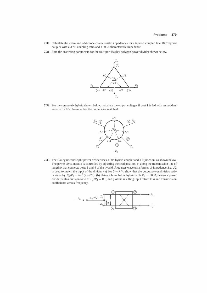
Problems
7.30 Calculate the even- and odd-mode characteristic impedances for a tapered coupled line 180◦ hybridcoupler with a 3 dB coupling ratio and a 50 � characteristic impedance.
7.31 Find the scattering parameters for the four-port Bagley polygon power divider shown below.
3
24 1
2Z0
3
Z0
Z0
Z0 Z0
�/2 �/2
�/4 �/4
7.32 For the symmetric hybrid shown below, calculate the output voltages if port 1 is fed with an incidentwave of 1 � 0 V. Assume that the outputs are matched.
�/2
�/4 �/4
�/4�/4
4 3
2
1
5
Z0 Z0
Z0 Z0
Z0
2Z0
7.33 The Bailey unequal-split power divider uses a 90◦ hybrid coupler and a T-junction, as shown below.The power division ratio is controlled by adjusting the feed position, a, along the transmission line oflength b that connects ports 1 and 4 of the hybrid. A quarter-wave transformer of impedance Z0/
√2
is used to match the input of the divider. (a) For b = λ/4, show that the output power division ratiois given by P3/P2 = tan2(πa/2b). (b) Using a branch-line hybrid with Z0 = 50 �, design a powerdivider with a division ratio of P3/P2 = 0.5, and plot the resulting input return loss and transmissioncoefficients versus frequency.
21
3
P2
P3Z0
Z0Pin
ab
Z0/ 2
4

C h a p t e r E i g h t
Microwave Filters
A filter is a two-port network used to control the frequency response at a certain pointin an RF or microwave system by providing transmission at frequencies within the passbandof the filter and attenuation in the stopband of the filter. Typical frequency responses includelow-pass, high-pass, bandpass, and band-reject characteristics. Applications can be found invirtually any type of RF or microwave communication, radar, or test and measurement system.
The development of filter theory and practice began in the years preceding World War II bypioneers such as Mason, Sykes, Darlington, Fano, Lawson, and Richards. The image parame-ter method of filter design was developed in the late 1930s and was useful for low-frequencyfilters in radio and telephony. In the early 1950s a group at Stanford Research Institute, consist-ing of G. Matthaei, L. Young, E. Jones, S. Cohn, and others, became very active in microwavefilter and coupler development. A voluminous handbook on filters and couplers resulted fromthis work and remains a valuable reference [1]. Today, most microwave filter design is donewith sophisticated computer-aided design (CAD) packages based on the insertion loss method.Because of continuing advances in network synthesis with distributed elements, the use of low-temperature superconductors and other new materials, and the incorporation of active devicesin filter circuits, microwave filter design remains an active research area.
We begin our discussion of filter theory and design with the frequency characteristics ofperiodic structures, which consist of a transmission line or waveguide periodically loaded withreactive elements. These structures are of interest in themselves because of their applicationto slow-wave components and traveling-wave amplifier design, and also because they exhibitbasic passband-stopband responses that lead to the image parameter method of filter design.
Filters designed using the image parameter method consist of a cascade of simpler two-port filter sections to provide the desired cutoff frequencies and attenuation characteristics butdo not allow the specification of a particular frequency response over the complete operatingrange. Thus, although the procedure is relatively simple, the design of filters by the imageparameter method often must be iterated many times to achieve the desired results.
A more modern procedure, called the insertion loss method, uses network synthesis tech-niques to design filters with a completely specified frequency response. The design is simplifiedby beginning with low-pass filter prototypes that are normalized in terms of impedance and
8.1 Periodic Structures
frequency. Transformations are then applied to convert the prototype designs to the desiredfrequency range and impedance level.
Both the image parameter and insertion loss methods of filter design lead to circuits usinglumped elements (capacitors and inductors). For microwave applications such designs usuallymust be modified to employ distributed elements consisting of transmission line sections. TheRichards transformation and the Kuroda identities provide this step. We will also discuss trans-mission line filters using stepped impedances and coupled lines; filters using coupled resonatorswill also be briefly described.
The subject of microwave filters is quite extensive due to the importance of these compo-nents in practical systems and the wide variety of possible implementations. Here we can treatonly the basic principles and some of the more common filter designs, and we refer the readerto references such as [1–4] for further discussion.
An infinite transmission line or waveguide periodically loaded with reactive elements isan example of a periodic structure. As shown in Figure 8.1, periodic structures can takevarious forms, depending on the transmission line media being used. Often the loadingelements are formed as discontinuities in the line itself, but in any case they can be modeledas lumped reactances in shunt (or series) on a transmission line, as shown in Figure 8.2.Periodic structures support slow-wave propagation (slower than the phase velocity of the
(a)
(b)
FIGURE 8.1 Examples of periodic structures. (a) Periodic stubs on a microstrip line. (b) Periodicdiaphragms in a waveguide.

Chapter 8: Microwave Filters
dZ0, k
jbjbjbjbjb jb
Unit cellz
Vn+1
In+1
+
–
Vn
In
+
–
FIGURE 8.2 Equivalent circuit of a periodically loaded transmission line. The unloaded line hascharacteristic impedance Z0 and propagation constant k.
unloaded line), and have passband and stopband characteristics similar to those of filters;they find application in traveling-wave tubes, masers, phase shifters, and antennas.
We first consider the propagation characteristics of the infinite loaded line shown in Fig-ure 8.2. Each unit cell of this line consists of a length, d, of transmission line with a shuntsusceptance across the midpoint of the line; the susceptance, b, is normalized to the char-acteristic impedance, Z0. If we consider the infinite line as being composed of a cascadeof identical two-port networks, we can relate the voltages and currents on either side of thenth unit cell using the ABCD matrix:
[VnIn
]=
[A BC D
] [Vn+1In+1
], (8.1)
where A, B, C, and D are the matrix parameters for a cascade of a transmission line sectionof length d/2, a shunt susceptance b, and another transmission line section of length d/2.From Table 4.1 we then have, in normalized form,
[A BC D
]=
⎡⎢⎢⎣ cos
θ
2j sin
θ
2
j sinθ
2cos
θ
2
⎤⎥⎥⎦[
1 0jb 1
]⎡⎢⎢⎣ cos
θ
2j sin
θ
2
j sinθ
2cos
θ
2
⎤⎥⎥⎦
=
⎡⎢⎢⎢⎣
(cos θ − b
2sin θ
)j(
sin θ + b2
cos θ − b2
)
j(
sin θ + b2
cos θ + b2
) (cos θ − b
2sin θ
)⎤⎥⎥⎥⎦, (8.2)
where θ = kd, and k is the propagation constant of the unloaded line. The reader can verifythat AD − BC = 1, as required for reciprocal networks.
For a wave propagating in the +z direction, we must have
V (z) = V (0)e−γ z, (8.3a)
I (z) = I (0)e−γ z, (8.3b)
for a phase reference at z = 0. Since the structure is infinitely long, the voltage and currentat the nth terminals can differ from the voltage and current at the n + 1 terminals only by

8.1 Periodic Structures
the propagation factor, e−γ d . Thus,Vn+1 = Vne−γ d , (8.4a)In+1 = Ine−γ d . (8.4b)
Using this result in (8.1) gives the following:[VnIn
]=
[A BC D
] [Vn+1In+1
]=
[Vn+1eγ d
In+1eγ d
],
or [A − eγ d B
C D − eγ d
] [Vn+1In+1
]= 0. (8.5)
For a nontrivial solution, the determinant of the above matrix must vanish:
AD + e2γ d − (A + D)eγ d − BC = 0, (8.6)
or, since AD − BC = 1,
1 + e2γ d − (A + D)eγ d = 0,
e−γ d + eγ d = A + D,
cosh γ d = A + D2
= cos θ − b2
sin θ, (8.7)
where (8.2) was used for the values of A and D. Now, if γ = α + jβ, we have that
cosh γ d = cosh αd cos βd + j sinh αd sin βd = cos θ − b2
sin θ. (8.8)
Since the right-hand side of (8.8) is purely real, we must have either α = 0 or β = 0.Case 1: α = 0, β �= 0. This case corresponds to a nonattenuated propagating wave on theperiodic structure, and defines the passband of the structure. Equation (8.8) reduces to
cos βd = cos θ − b2
sin θ, (8.9a)
which can be solved for β if the magnitude of the right-hand side is less than or equal tounity. Note that there are an infinite number of values of β that can satisfy (8.9a).Case 2: α �= 0, β = 0, π . In this case the wave does not propagate, but is attenuated alongthe line; this defines the stopband of the structure. Because the line is lossless, power is notdissipated, but is reflected back to the input of the line. The magnitude of (8.8) reduces to
cosh αd =∣∣∣∣cos θ − b
2sin θ
∣∣∣∣ ≥ 1, (8.9b)
which has only one solution (α > 0) for positively traveling waves; α < 0 applies for nega-tively traveling waves. If cos θ − (b/2) sin θ ≤ −1, (8.9b) is obtained from (8.8) by lettingβ = π ; then all the lumped loads on the line are λ/2 apart, yielding an input impedancethe same as if β = 0.
Thus, depending on the frequency and normalized susceptance values, the periodicallyloaded line will exhibit either passbands or stopbands, and so can be considered as a typeof filter. It is important to note that the voltage and current waves defined in (8.3) and (8.4)are meaningful only when measured at the terminals of the unit cells, and do not apply tovoltages and currents that may exist at points within a unit cell. These waves are similar tothe elastic waves (Bloch waves) that propagate through periodic crystal lattices.

Chapter 8: Microwave Filters
Besides the propagation constant of the waves on the periodically loaded line, wewill also be interested in the characteristic impedance for these waves. We can define acharacteristic impedance at the unit cell terminals as
Z B = Z0Vn+1
In+1, (8.10)
since Vn+1 and In+1 in the above derivation were normalized quantities. This impedanceis also referred to as the Bloch impedance. From (8.5) we have that
(A − eγ d)Vn+1 + B In+1 = 0,
so (8.10) yields
Z B = −B Z0
A − eγ d .
From (8.6) we can solve for eγ d in terms of A and D as follows:
eγ d = (A + D) ± √(A + D)2 − 42
.
Then the Bloch impedance has two solutions given by
Z±B = −2B Z0
A − D ∓ √(A + D)2 − 4
. (8.11)
For symmetric unit cells (as assumed in Figure 8.2) we will always have A = D. In thiscase (8.11) reduces to
Z±B = ±B Z0√
A2 − 1. (8.12)
The ± solutions correspond to the characteristic impedance for positively and negativelytraveling waves, respectively. For symmetric networks these impedances are the same ex-cept for the sign; the characteristic impedance for a negatively traveling wave is negativebecause we have defined In in Figure 8.2 as always being in the positive direction.
From (8.2) we see that B is always purely imaginary. If α = 0, β �= 0 (passband), then(8.7) shows that cosh γ d = A ≤ 1 (for symmetric networks), and (8.12) shows that Z B willbe real. If α �= 0, β = 0 (stopband), then (8.7) shows that cosh γ d = A ≥ 1, and (8.12)shows that Z B is imaginary. This situation is similar to that for the wave impedance of awaveguide, which is real for propagating modes and imaginary for cutoff, or evanescent,modes.
Next consider a truncated periodic structure terminated in a load impedance ZL , as shownin Figure 8.3. At the terminals of an arbitrary unit cell, the incident and reflected voltages
Unitcell
Unitcell
Unitcell
In
Vn
+
–
IN
VN ZL
+
–
FIGURE 8.3 A periodic structure terminated in a normalized load impedance ZL .

8.1 Periodic Structures
and currents can be written as (assuming operation in the passband)
Vn = V +0 e− jβnd + V −
0 e jβnd (8.13a)
In = I +0 e− jβnd + I −
0 e jβnd = V +0
Z+B
e− jβnd + V −0
Z−B
e jβnd (8.13b)
where we have replaced γ z in (8.3) with jβnd since we are interested only in terminalquantities.
Now define the following incident and reflected voltages at the nth unit cell:
V +n = V +
0 e− jβnd (8.14a)
V −n = V −
0 e jβnd (8.14b)
Then (8.13) can be written as
Vn = V +n + V −
n , (8.15a)
In = V +n
Z+B
+ V −n
Z−B
. (8.15b)
At the load, where n = N , we have
VN = V +N + V −
N = ZL IN = ZL
(V +
NZ+
B+ V −
NZ−
B
), (8.16)
and the reflection coefficient at the load can be found as
� = V −N
V +N
= − ZL/Z+B − 1
ZL/Z−B − 1
. (8.17)
If the unit cell network is symmetric (A = D), then Z+B = −Z−
B = Z B , which reduces(8.17) to the familiar result
� = ZL − Z B
ZL + Z B. (8.18)
In order to avoid reflections on the terminated periodic structure we must have ZL =Z B, which is real for a lossless structure operating in a passband. If necessary, a quarter-wave transformer can be used between the periodically loaded line and the load.
β
When studying the passband and stopband characteristics of a periodic structure, it is usefulto plot the propagation constant, β, versus the propagation constant of the unloaded line,k (or ω). Such a graph is called a k-β diagram, or Brillouin diagram, after L. Brillouin, aphysicist who studied wave propagation in periodic crystal structures.
The k-β diagram can be plotted from (8.9a), which is the dispersion relation for ageneral periodic structure. In fact, a k-β diagram can be used to study the dispersion char-acteristics of many types of microwave components and transmission lines. For instance,consider the dispersion relation for a waveguide mode:
β =√
k2 − k2c , or k =
√β2 + k2
c , (8.19)
where kc is the cutoff wave number of the mode, k is the free-space wave number, and β
is the propagation constant of the mode. Relation (8.19) is plotted in the k-β diagram of

Chapter 8: Microwave Filters
k
�
Propagation
Operatingpoint
Cutoff
k = ��
kc
Slope = vg/c
Slope = vp/c
0
FIGURE 8.4 k-β diagram for a waveguide mode.
Figure 8.4. For values of k < kc there is no real solution for β, so the mode is nonpropa-gating. For k > kc the mode propagates, and k approaches β for large values of β (TEMpropagation).
The k-β diagram is also useful for interpreting the various wave velocities associatedwith a dispersive structure. The phase velocity is
vp = ω
β= c
kβ
, (8.20)
which is seen to be equal to c (speed of light) times the slope of the line from the origin tothe operating point on the k-β diagram. The group velocity is
vg = dω
dβ= c
dkdβ
, (8.21)
which is the slope of the k-β curve at the operating point. Thus, referring to Figure 8.4,we see that the phase velocity for a propagating waveguide mode is infinite at cutoff andapproaches c (from above) as k increases. The group velocity, however, is zero at cutoff andapproaches c (from below) as k increases. We finish our discussion of periodic structureswith a practical example of a capacitively loaded line.
EXAMPLE 8.1 ANALYSIS OF A PERIODIC STRUCTURE
Consider the periodic capacitively loaded line shown in Figure 8.5 (such a linemay be implemented as in Figure 8.1, with short capacitive stubs). If Z0 = 50 �,d = 1.0 cm, and C0 = 2.666 pF, sketch the k-β diagram and compute the prop-agation constant, phase velocity, and Bloch impedance at f = 3.0 GHz. Assumek = k0.
d
C0 C0 C0 C0 C0
Z0, k
FIGURE 8.5 A capacitively loaded line.

8.1 Periodic Structures
SolutionWe can rewrite the dispersion relation of (8.9a) as
cos βd = cos k0d −(
C0 Z0c2d
)k0d sin k0d.
Then
C0 Z0c2d
= (2.666 × 10⁻¹²)(50)(3 × 10⁸)
2(0.01)= 2.0,
so we have
cos βd = cos k0d − 2k0d sin k0d.
The most straightforward way to proceed at this point is to numerically evaluatethe right-hand side of the above equation for a set of values of k0d starting at zero.When the magnitude of the right-hand side is unity or less, we have a passband andcan solve for βd . Otherwise we have a stopband. Calculation shows that the firstpassband exists for 0 ≤ k0d ≤ 0.96. The second passband does not begin untilthe sin k0d term changes sign at k0d = π . As k0d increases, an infinite numberof passbands are possible, but they become narrower. Figure 8.6 shows the k-βdiagram for the first two passbands.
At 3.0 GHz, we have
k0d = 2π(3 × 10⁹)
3 × 10⁸ (0.01) = 0.6283 = 36◦,
so βd = 1.5 and the propagation constant is β = 150 rad/m. The phase velocityis
vp = k0cβ
= 0.62831.5
c = 0.42c,
which is much less than the speed of light, indicating that this is a slow-wave
1
2
3
4
k0d
–3 –2 –1 0 1 2 3 �d
–� �Passband
Passband
FIGURE 8.6 k-β diagram for Example 8.1.

Chapter 8: Microwave Filters
structure. To evaluate the Bloch impedance, we use (8.2) and (8.12):
b2
= ωC0 Z0
2= 1.256,
θ = k0d = 36◦,
A = cos θ − b2
sin θ = 0.0707,
B = j(
sin θ + b2
cos θ − b2
)= j0.3479.
Then,
Z B = B Z0√A2 − 1
= ( j0.3479)(50)
j√
1 − (0.0707)2= 17.4 �.
■
The image parameter method of filter design involves the specification of passband andstopband characteristics for a cascade of simple two-port networks, and so is related in con-cept to the periodic structures of Section 8.1. The method is relatively simple but has thedisadvantage that an arbitrary frequency response cannot be incorporated into the design.This is in contrast to the insertion loss method, which is the subject of the following section.Nevertheless, the image parameter method is useful for simple filters, and it provides a linkbetween infinite periodic structures and practical filter design. The image parameter methodalso finds application in solid-state traveling-wave amplifier design.
We begin with definitions of the image impedances and voltage transfer function for anarbitrary reciprocal two-port network; these results are required for the analysis and designof filters by the image parameter method.
Consider the arbitrary two-port network shown in Figure 8.7, where the network isspecified by its ABCD parameters. Note that the reference direction for the current at port 2has been chosen according to the convention for ABCD parameters. The image impedances,Zi1 and Zi2, are defined for this network as follows:
Zi1 = input impedance at port 1 when port 2 is terminated with Zi2
Zi2 = input impedance at port 2 when port 1 is terminated with Zi1.
Thus both ports are matched when terminated in their image impedances. We can deriveexpressions for the image impedances in terms of the ABCD parameters of the network.
I2I1
V2 Zi2
+
–V1Zi1
+
–
AC
BD
Z in 1 Z in 2
FIGURE 8.7 A two-port network terminated in its image impedances.

8.2 Filter Design by the Image Parameter Method
The port voltages and currents are related as
V1 = AV2 + B I2, (8.22a)
I1 = CV2 + DI2. (8.22b)
The input impedance at port 1, with port 2 terminated in Zi2, is
Z in1 = V1
I1= AV2 + B I2
CV2 + DI2= AZi2 + B
C Zi2 + D, (8.23)
since V2 = Zi2 I2.Now solve (8.22) for V2, I2 by inverting the ABCD matrix. Since AD − BC = 1 for
a reciprocal network, we obtain
V2 = DV1 − B I1, (8.24a)
I2 = −CV1 + AI1. (8.24b)
Then the input impedance at port 2, with port 1 terminated in Zi1, can be found as
Z in2 = −V2
I2= − DV1 − B I1
−CV1 + AI1= DZi1 + B
C Zi1 + A, (8.25)
since V1 = −Zi1 I1 (circuit of Figure 8.7).We desire that Zin1 = Zi1 and Zin2 = Zi2, so (8.23) and (8.25) give two equations for
the image impedances:
Zi1(C Zi2 + D) = AZi2 + B, (8.26a)
Zi1 D − B = Zi2(A − C Zi1). (8.26b)
Solving for Zi1 and Zi2 gives
Zi1 =√
ABC D
, (8.27a)
Zi2 =√
B DAC
, (8.27b)
with Zi2 = DZi1/A. If the network is symmetric, then A = D and Zi1 = Zi2 as expected.Now consider the voltage transfer function for a two-port network terminated in its
image impedances. With reference to Figure 8.8 and (8.24a), the output voltage at port 2can be expressed as
V2 = DV1 − B I1 =(
D − BZi1
)V1 (8.28)
I2I1
V2 Zi2
+
–V1
Zi1 +
–
AC
BD
Zi1 Zi2
2V1
FIGURE 8.8 A two-port network terminated in its image impedances and driven with a voltagegenerator.
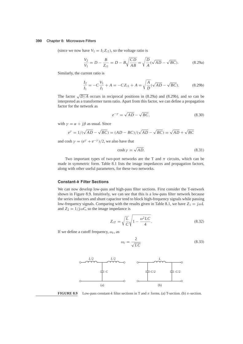
Chapter 8: Microwave Filters
(since we now have V1 = I1 Zi1), so the voltage ratio is
V2
V1= D − B
Zi1= D − B
√C DAB
=√
DA
(√
AD − √BC). (8.29a)
Similarly, the current ratio is
I2
I1= −C
V1
I1+ A = −C Zi1 + A =
√AD
(√
AD − √BC). (8.29b)
The factor√
D/A occurs in reciprocal positions in (8.29a) and (8.29b), and so can beinterpreted as a transformer turns ratio. Apart from this factor, we can define a propagationfactor for the network as
e−γ = √AD − √
BC, (8.30)
with γ = α + jβ as usual. Since
eγ = 1/(√
AD − √BC) = (AD − BC)/(
√AD − √
BC) = √AD + √
BC
and cosh γ = (eγ + e−γ )/2, we also have that
cosh γ = √AD. (8.31)
Two important types of two-port networks are the T and π circuits, which can bemade in symmetric form. Table 8.1 lists the image impedances and propagation factors,along with other useful parameters, for these two networks.
We can now develop low-pass and high-pass filter sections. First consider the T-networkshown in Figure 8.9. Intuitively, we can see that this is a low-pass filter network becausethe series inductors and shunt capacitor tend to block high-frequency signals while passinglow-frequency signals. Comparing with the results given in Table 8.1, we have Z1 = jωLand Z2 = 1/jωC, so the image impedance is
ZiT =√
LC
√1 − ω2LC
4. (8.32)
If we define a cutoff frequency, ωc, as
ωc = 2√LC
(8.33)
L /2 L /2
C C/2 C/2
L
(a) (b)
FIGURE 8.9 Low-pass constant-k filter sections in T and π forms. (a) T-section. (b) π -section.

8.2 Filter Design by the Image Parameter Method
and a nominal characteristic impedance, R0, as
R0 =√
LC
= k, (8.34)
where k is a constant, then we can rewrite (8.32) as
ZiT = R0
√1 − ω2
ω2c. (8.35)
Then ZiT = R0 for ω = 0.The propagation factor, also from Table 8.1, is
eγ = 1 − 2ω2
ω2c
+ 2ω
ωc
√ω2
ω2c
− 1. (8.36)
Now consider two frequency regions:1. For ω < ωc: This is the passband of the filter section. Equation (8.35) shows that
ZiT is real, and (8.36) shows that γ is imaginary, since ω2/ω2c − 1 is negative and
|eγ | = 1:
|eγ |2 =(
1 − 2ω2
ω2c
)2
+ 4ω2
ω2c
(1 − ω2
ω2c
)= 1.
2. For ω > ωc: This is the stopband of the filter section. Equation (8.35) shows that ZiTis imaginary, and (8.36) shows that eγ is real and −1 < eγ < 0 (as seen from thelimits as ω → ωc and ω → ∞). The attenuation rate for ω � ωc is 40 dB/decade.
Typical phase and attenuation constants are sketched in Figure 8.10. Observe that theattenuation, α, is zero or relatively small near the cutoff frequency, although α → ∞ as
TABLE 8.1 Image Parameters for T- and π -Networks
Z1/2 Z1/2
Z2
Z1
2Z2 2Z2
T-Network π -Network
ABCD parameters: ABCD parameters:A = 1 + Z1/2Z2 A = 1 + Z1/2Z2B = Z1 + Z2
1/4Z2 B = Z1C = 1/Z2 C = 1/Z2 + Z1/4Z2
2D = 1 + Z1/2Z2 D = 1 + Z1/2Z2Z parameters: Y parameters:Z11 = Z22 = Z2 + Z1/2 Y11 = Y22 = 1/Z1 + 1/2Z2Z12 = Z21 = Z2 Y12 = Y21 = 1/Z1Image impedance: Image impedance:ZiT =
√Z1 Z2
√1 + Z1/4Z2 Zi π =
√Z1 Z2/
√1 + Z1/4Z2 = Z1 Z2/ZiT
Propagation constant: Propagation constant:
eγ = 1 + Z1/2Z2 +√
Z1/Z2 + Z21/4Z2
2 eγ = 1 + Z1/2Z2 +√
Z1/Z2 + Z21/4Z2
2
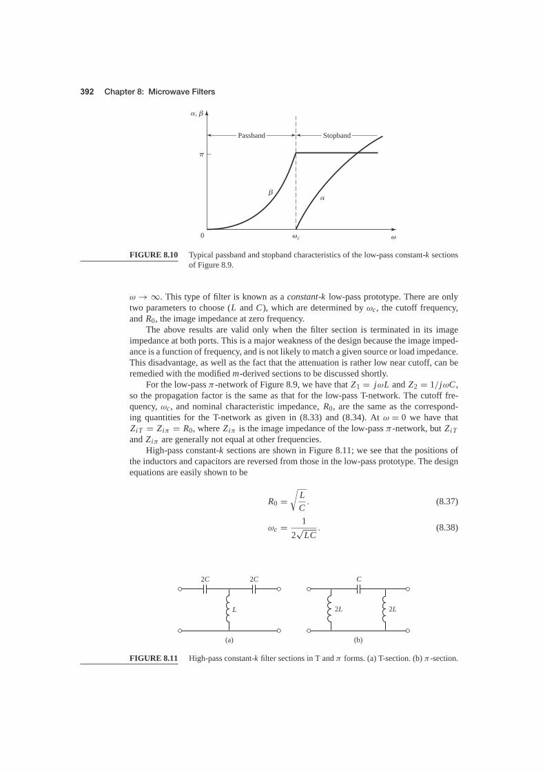
Chapter 8: Microwave Filters
0
Passband Stopband
�, �
�
��
c
FIGURE 8.10 Typical passband and stopband characteristics of the low-pass constant-k sectionsof Figure 8.9.
ω → ∞. This type of filter is known as a constant-k low-pass prototype. There are onlytwo parameters to choose (L and C), which are determined by ωc, the cutoff frequency,and R0, the image impedance at zero frequency.
The above results are valid only when the filter section is terminated in its imageimpedance at both ports. This is a major weakness of the design because the image imped-ance is a function of frequency, and is not likely to match a given source or load impedance.This disadvantage, as well as the fact that the attenuation is rather low near cutoff, can beremedied with the modified m-derived sections to be discussed shortly.
For the low-pass π-network of Figure 8.9, we have that Z1 = jωL and Z2 = 1/jωC ,so the propagation factor is the same as that for the low-pass T-network. The cutoff fre-quency, ωc, and nominal characteristic impedance, R0, are the same as the correspond-ing quantities for the T-network as given in (8.33) and (8.34). At ω = 0 we have thatZiT = Ziπ = R0, where Ziπ is the image impedance of the low-pass π -network, but ZiTand Ziπ are generally not equal at other frequencies.
High-pass constant-k sections are shown in Figure 8.11; we see that the positions ofthe inductors and capacitors are reversed from those in the low-pass prototype. The designequations are easily shown to be
R0 =√
LC
. (8.37)
ωc = 12√
LC. (8.38)
2C 2C
2L 2LL
C
(a) (b)
FIGURE 8.11 High-pass constant-k filter sections in T and π forms. (a) T-section. (b) π -section.

8.2 Filter Design by the Image Parameter Method
1 – m2
4m
(a)
Z1/2 Z1/2
Z2
(c)
mZ1/2 mZ1/2
Z2/m
Z1
(b)
' '
'
Z1/2 Z1/2
Z2
FIGURE 8.12 Development of an m-derived filter section from a constant-k section. (a) Constant-k section. (b) General m-derived section. (c) Final m-derived section.
We have seen that the constant-k filter section suffers from the disadvantages of a relativelyslow attenuation rate past cutoff, and a nonconstant image impedance. The m-derived filtersection is a modification of the constant-k section designed to overcome these problems. Asshown in Figure 8.12a, b the impedances Z1 and Z2 in a constant-k T-section are replacedwith Z ′
1 and Z ′2, and we let
Z ′1 = m Z1. (8.39)
Then we choose Z ′2 to obtain the same value of ZiT as for the constant-k section. Thus,
from Table 8.1,
ZiT =√
Z1 Z2 + Z21
4=
√Z ′
1 Z ′2 + Z ′2
14
=√
m Z1 Z ′2 + m2 Z2
14
. (8.40)
Solving for Z ′2 gives
Z ′2 = Z2
m+ Z1
4m− m Z1
4= Z2
m+ (1 − m2)
4mZ1. (8.41)
Because the impedances Z1 and Z2 represent reactive elements, Z ′2 represents two el-
ements in series, as indicated in Figure 8.12c. Note that m = 1 reduces to the originalconstant-k section.
For a low-pass filter, we have Z1 = jωL and Z2 = 1/jωC . Then (8.39) and (8.41)give the m-derived components as
Z ′1 = jωLm, (8.42a)
Z ′2 = 1
jωCm+ (1 − m2)
4mjωL , (8.42b)
which results in the circuit of Figure 8.13. Now consider the propagation factor for the

Chapter 8: Microwave Filters
mL/2 mL/2
mC
(a) (b)
1 – m2
4m L1 – m2
4m C
L/m
2C/m 2C/m
FIGURE 8.13 m-Derived filter sections. (a) Low-pass T-section. (b) High-pass T-section.
m-derived section. From Table 8.1,
eγ = 1 + Z ′1
2Z ′2
+√
Z ′1
Z ′2
(1 + Z ′
14Z ′
2
). (8.43)
For the low-pass m-derived filter,
Z ′1
Z ′2
= jωLm(1/jωCm) + jωL(1 − m2)/4m
= −(2ωm/ωc)2
1 − (1 − m2)(ω/ωc)2 ,
where ωc = 2/√
LC as before. Then,
1 + Z ′1
4Z ′2
= 1 − (ω/ωc)2
1 − (1 − m2)(ω/ωc)2 .
If we restrict 0 < m < 1, then these results show that eγ is real and |eγ | > 1 for ω > ωc.Thus the stopband begins at ω = ωc, as for the constant-k section. However, when ω =ω∞, where
ω∞ = ωc√1 − m2
, (8.44)
the denominators vanish and eγ becomes infinite, implying infinite attenuation. Physically,this pole in the attenuation characteristic is caused by the resonance of the series LC res-onator in the shunt arm of the T; this is easily verified by showing that the resonant fre-quency of this LC resonator is ω∞. Note that (8.44) indicates that ω∞ > ωc, so infiniteattenuation occurs after the cutoff frequency, ωc, as illustrated in Figure 8.14. The positionof the pole at ω∞ can be controlled with the value of m.
0
�
c
m-derivedattenuation
Compositeresponse
Constant-kattenuation
FIGURE 8.14 Typical attenuation responses for constant-k, m-derived, and composite filters.

8.2 Filter Design by the Image Parameter Method
Z2/m Z2/m
(1 – m2)4m
Z1(1 – m2)
4mZ1
mZ1/2 mZ1/2 mZ1/2 mZ1/2
(a)
(b)
2Z2m
2(1 – m2)Z14m
mZ1
FIGURE 8.15 Development of an m-derived π -section. (a) Infinite cascade of m-derivedT-sections. (b) A de-embedded π -equivalent.
We now have a very sharp cutoff response, but one problem with the m-derived sectionis that its attenuation decreases for ω > ω∞. Since it is often desirable to have infiniteattenuation as ω → ∞, the m-derived section can be cascaded with a constant-k section togive the composite attenuation response shown in Figure 8.14.
The m-derived T-section was designed so that its image impedance was identical tothat of the constant-k section (independent of m), so we still have the problem of a non-constant image impedance. However, the image impedance of the π -equivalent will dependon m, and this extra degree of freedom can be used to design an optimum matching section.
The easiest way to obtain the corresponding π -section is to consider it as a pieceof an infinite cascade of m-derived T-sections, as shown in Figure 8.15. Then the imageimpedance of this network is, using the results of Table 8.1 and (8.35),
Ziπ = Z ′1 Z ′
2ZiT
= Z1 Z2 + Z21(1 − m2)/4
R0√
1 − (ω/ωc)2. (8.45)
Now Z1 Z2 = L/C = R20 and Z2
1 = −ω2L2 = −4R20(ω/ωc)
2, so (8.45) reduces to
Ziπ = 1 − (1 − m2)(ω/ωc)2√
1 − (ω/ωc)2R0. (8.46)
Since this impedance is a function of m, we can choose m to minimize the variation of Ziπover the passband of the filter. Figure 8.16 shows this variation with frequency for severalvalues of m; a value of m = 0.6 generally gives the best results.
This type of m-derived section can then be used at the input and output of the filter toprovide a nearly constant impedance match to and from R0. However, the image impedanceof the constant-k and m-derived T-sections, ZiT, does not match Ziπ; this problem can besurmounted by bisecting the π-sections, as shown in Figure 8.17. The image impedances

Chapter 8: Microwave Filters
c 0
Zi�
R0
m = 0.3
m = 0.6
m = 1
FIGURE 8.16 Variation of Ziπ in the passband of a low-pass m-derived section for various valuesof m.
of this circuit are Zi1 = ZiT and Zi2 = Ziπ , which can be shown by finding its ABCDparameters:
A = 1 + Z ′1
4Z ′2, (8.47a)
B = Z ′1
2, (8.47b)
C = 12Z ′
2, (8.47c)
D = 1, (8.47d)
and then using (8.27) for Zi1 and Zi2:
Zi1 =√
Z ′1 Z ′
2 + Z ′21
4= ZiT , (8.48a)
Zi2 =√
Z ′1 Z ′
21 + Z ′
1/4Z ′2
= Z ′1 Z ′
2ZiT
= Ziπ, (8.48b)
where (8.40) has been used for ZiT .
By combining in cascade the constant-k, m-derived sharp cutoff and the m-derived match-ing sections we can realize a filter with the desired attenuation and matching properties.
Z1/2
Zi1 = ZiT Zi2 = Zi�2Z2
'
'
FIGURE 8.17 A bisected π -section used to match Ziπ to ZiT .

8.2 Filter Design by the Image Parameter Method
m = 0.612 �
m = 0.6m < 0.6T 1
2 �
Constant-kT
~R0 ~R0
Matchingsection
Matchingsection
High-fcutoff
Sharpcutoff
ZiT ZiT ZiT
FIGURE 8.18 The final four-stage composite filter.
This type of design is called a composite filter, and is shown in Figure 8.18. The sharp-cutoff section, with m < 0.6, places an attenuation pole near the cutoff frequency to providea sharp attenuation response; the constant-k section provides high attenuation further intothe stopband. The bisected-π sections at the ends of the filter match the nominal sourceand load impedance, R0, to the internal image impedances, ZiT , of the constant-k andm-derived sections. Table 8.2 summarizes the design equations for low- and high-pass
TABLE 8.2 Summary of Composite Filter Design
Low-Pass High-Pass
(1 – m2)2m L
(1 – m2)2m L
mL/2mL/2
mC2
L/m
2C/m 2C/m
L /2 L /2 2C 2C
mC
(1 – m2)4m L
mL/2mL/2
mC
2
R0R0
–
–
ZiT
(1 – m2)2m
C(1 – m2)
2mC
(1 – m2)4m
C
2L/m 2L/m
2C/m 2C/m
R0R0
–
–
ZiT
C L
Constant-k T section Constant-k T section
R0 = L /Cωc = 2/ LC
L = 2R0/ cC = 2/ cR0
m-derived T section
L, C Same as constant-k section
m =1 – ( c/ ∞)2 for sharp-cutoff
0.6 for matching
Bisected- matching section
L, C Same as constant-k section
m =1 – ( ∞/ c)2 for sharp-cutoff
0.6 for matching
Bisected- matching section
R0 = L /Cc = 1/2 LC
L = R0/2 cC = 1/2 cR0
m-derived T section

Chapter 8: Microwave Filters
composite filters; notice that once the cutoff frequency and impedance are specified, thereis only one degree of freedom (the value of m for the sharp-cutoff section) left to controlthe filter response. The following example illustrates the design procedure.
EXAMPLE 8.2 LOW-PASS COMPOSITE FILTER DESIGN
Design a low-pass composite filter with a cutoff frequency of 2 MHz and imped-ance of 75 �. Place the infinite attenuation pole at 2.05 MHz, and plot the fre-quency response from 0 to 4 MHz.
SolutionAll of the component values can be found from Table 8.2. For the constant-ksection
L = 2R0
ωc= 11.94 μH, C = 2
R0ωc= 2.122 nF.
For the m-derived sharp-cutoff section
m =√
1 −( fc
f∞
)2 = 0.2195,
mL2
= 1.310 μH,
mC = 465.8 pF,
1 − m2
4mL = 12.94 μH.
For the m = 0.6 matching sectionsmL2
= 3.582 μH,
mC2
= 636.5 pF,
1 − m2
2mL = 6.368 μH.
The completed filter circuit is shown in Figure 8.19; the series pairs of induc-tors between the sections have been combined. Figure 8.20 shows the resultingfrequency response for |S12|. Note the sharp dip at f = 2.05 MHz due to them = 0.2195 section, and the pole at 2.50 MHz, which is due to the m = 0.6matching sections. ■
3.582 �H 1.310 �H 1.310 �H 3.582 �H5.97 �H 5.97 �H
6.368 �H
636.5 pF
12.94 �H
465.8 pF
6.368 �H
636.5 pF
2122 pF
Matching Constant-k m-derived Matching
FIGURE 8.19 Low-pass composite filter for Example 8.2.
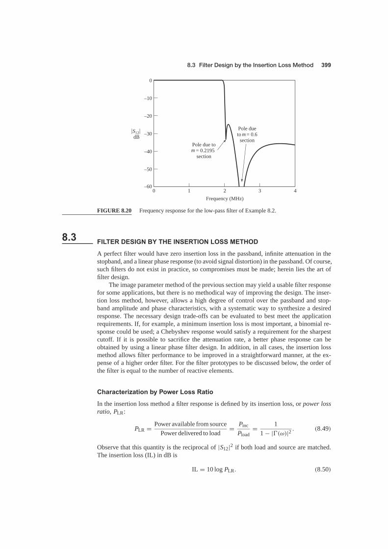
8.3 Filter Design by the Insertion Loss Method
0 1 2 3 4–60
–50
–40
–30
–20
–10
0
Pole dueto = 0.6
sectionPole due to = 0.2195
section
⎜S12⎜dB
Frequency (MHz)
m
m
FIGURE 8.20 Frequency response for the low-pass filter of Example 8.2.
A perfect filter would have zero insertion loss in the passband, infinite attenuation in thestopband, and a linear phase response (to avoid signal distortion) in the passband. Of course,such filters do not exist in practice, so compromises must be made; herein lies the art offilter design.
The image parameter method of the previous section may yield a usable filter responsefor some applications, but there is no methodical way of improving the design. The inser-tion loss method, however, allows a high degree of control over the passband and stop-band amplitude and phase characteristics, with a systematic way to synthesize a desiredresponse. The necessary design trade-offs can be evaluated to best meet the applicationrequirements. If, for example, a minimum insertion loss is most important, a binomial re-sponse could be used; a Chebyshev response would satisfy a requirement for the sharpestcutoff. If it is possible to sacrifice the attenuation rate, a better phase response can beobtained by using a linear phase filter design. In addition, in all cases, the insertion lossmethod allows filter performance to be improved in a straightforward manner, at the ex-pense of a higher order filter. For the filter prototypes to be discussed below, the order ofthe filter is equal to the number of reactive elements.
In the insertion loss method a filter response is defined by its insertion loss, or power lossratio, PLR:
PLR = Power available from sourcePower delivered to load
= Pinc
Pload= 1
1 − |�(ω)|2 . (8.49)
Observe that this quantity is the reciprocal of |S12|2 if both load and source are matched.The insertion loss (IL) in dB is
IL = 10 log PLR. (8.50)

Chapter 8: Microwave Filters
From Section 4.1 we know that |�(ω)|2 is an even function of ω; therefore it can beexpressed as a polynomial in ω2. Thus we can write
|�(ω)|2 = M(ω2)
M(ω2) + N (ω2), (8.51)
where M and N are real polynomials in ω2. Substituting this form in (8.49) gives thefollowing:
PLR = 1 + M(ω2)
N (ω2). (8.52)
For a filter to be physically realizable its power loss ratio must be of the form in (8.52).Notice that specifying the power loss ratio simultaneously constrains the magnitude of thereflection coefficient, |�(ω)|. We now discuss some practical filter responses.
Maximally flat: This characteristic is also called the binomial or Butterworth response, andis optimum in the sense that it provides the flattest possible passband response for a givenfilter complexity, or order. For a low-pass filter, it is specified by
PLR = 1 + k2(
ω
ωc
)2N, (8.53)
where N is the order of the filter and ωc is the cutoff frequency. The passband extendsfrom ω = 0 to ω = ωc; at the band edge the power loss ratio is 1 + k2. If we choose thisas the −3 dB point, as is common, we have k = 1, which we will assume from now on.For ω > ωc, the attenuation increases monotonically with frequency, as shown in Figure8.21. For ω � ωc, PLR k2(ω/ωc)
2N , which shows that the insertion loss increases at therate of 20N dB/decade. Like the binomial response for multisection quarter-wave matchingtransformers, the first (2N − 1) derivatives of (8.53) are zero at ω = 0.
Equal ripple: If a Chebyshev polynomial is used to specify the insertion loss of an N th-order low-pass filter as
PLR = 1 + k2T 2N
(ω
ωc
), (8.54)
then a sharper cutoff will result, although the passband response will have ripples of ampli-tude 1 + k2, as shown in Figure 8.21, since TN (x) oscillates between ±1 for |x |21. Thus,
FIGURE 8.21 Maximally flat and equal-ripple low-pass filter responses (N = 3).

8.3 Filter Design by the Insertion Loss Method
PLR
/c0 1 2
Amin
Amax
FIGURE 8.22 Elliptic function low-pass filter response.
k2 determines the passband ripple level. For large x, TN (x) 12 (2x)N, so for ω � ωc the
insertion loss becomes
PLR k2
4
(2ω
ωc
)2N,
which also increases at the rate of 20N dB/decade. However, the insertion loss for theChebyshev case is (22N )/4 greater than the binomial response at any given frequencywhere ω � ωc.
Elliptic function: The maximally flat and equal-ripple responses both have monotonicallyincreasing attenuation in the stopband. In many applications it is adequate to specify a min-imum stopband attenuation, in which case a better cutoff rate can be obtained. Such filtersare called elliptic function filters [3], and they have equal-ripple responses in the passbandas well as in the stopband, as shown in Figure 8.22. The maximum attenuation in the pass-band, Amax, can be specified, as well as the minimum attenuation in the stopband, Amin.Elliptic function filters are difficult to synthesize, so we will not consider them further; theinterested reader is referred to reference [3].
Linear phase: The above filters specify the amplitude response, but in some applications(such as multiplexing filters for communication systems) it is important to have a linearphase response in the passband to avoid signal distortion. Since a sharp-cutoff response isgenerally incompatible with a good phase response, the phase response of a filter must bedeliberately synthesized, usually resulting in an inferior attenuation characteristic. A linearphase characteristic can be achieved with the following phase response:
φ(ω) = Aω
[1 + p
(ω
ωc
)2N], (8.55)
where φ(ω) is the phase of the voltage transfer function of the filter, and p is a constant. Arelated quantity is the group delay, defined as
τd = dφ
dω= A
[1 + p(2N + 1)
(ω
ωc
)2N], (8.56)
which shows that the group delay for a linear phase filter is a maximally flat function.More general filter specifications can be obtained, but the above cases are the most
common. We will next discuss the design of low-pass filter prototypes that are normalizedin terms of impedance and frequency; this normalization simplifies the design of filters

Chapter 8: Microwave Filters
Filterspecifications
Low-passprototype
designScaling andconversion Implementation
FIGURE 8.23 The process of filter design by the insertion loss method.
for arbitrary frequency, impedance, and type (low-pass, high-pass, bandpass, or bandstop).The low-pass prototypes are then scaled to the desired frequency and impedance, and thelumped-element components replaced with distributed circuit elements for implementationat microwave frequencies. This design process is illustrated in Figure 8.23.
Consider the two-element low-pass filter prototype shown in Figure 8.24; we will derivethe normalized element values, L and C , for a maximally flat response. We assume a sourceimpedance of 1 �, and a cutoff frequency ωc = 1 rad/sec. From (8.53), the desired powerloss ratio will be, for N = 2,
PLR = 1 + ω4. (8.57)
The input impedance of this filter is
Z in = jωL + R(1 − jωRC)
1 + ω2 R2C2 . (8.58)
Because
� = Z in − 1Z in + 1
,
the power loss ratio can be written as
PLR = 11 − |�|2 = 1
1 − [(Zin − 1
)/(Zin + 1
)][(Z∗
in − 1)/(Z∗
in + 1)] = |Z in + 1|2
2(Zin + Z∗
in) .
(8.59)
Now
Zin + Z∗in = 2R
1 + ω2 R2C2 ,
|Z in + 1|2 =(
R1 + ω2 R2C2 + 1
)2+
(ωL − ωC R2
1 + ω2 R2C2
)2
,
1 L
C R
Zin
FIGURE 8.24 Low-pass filter prototype, N = 2.
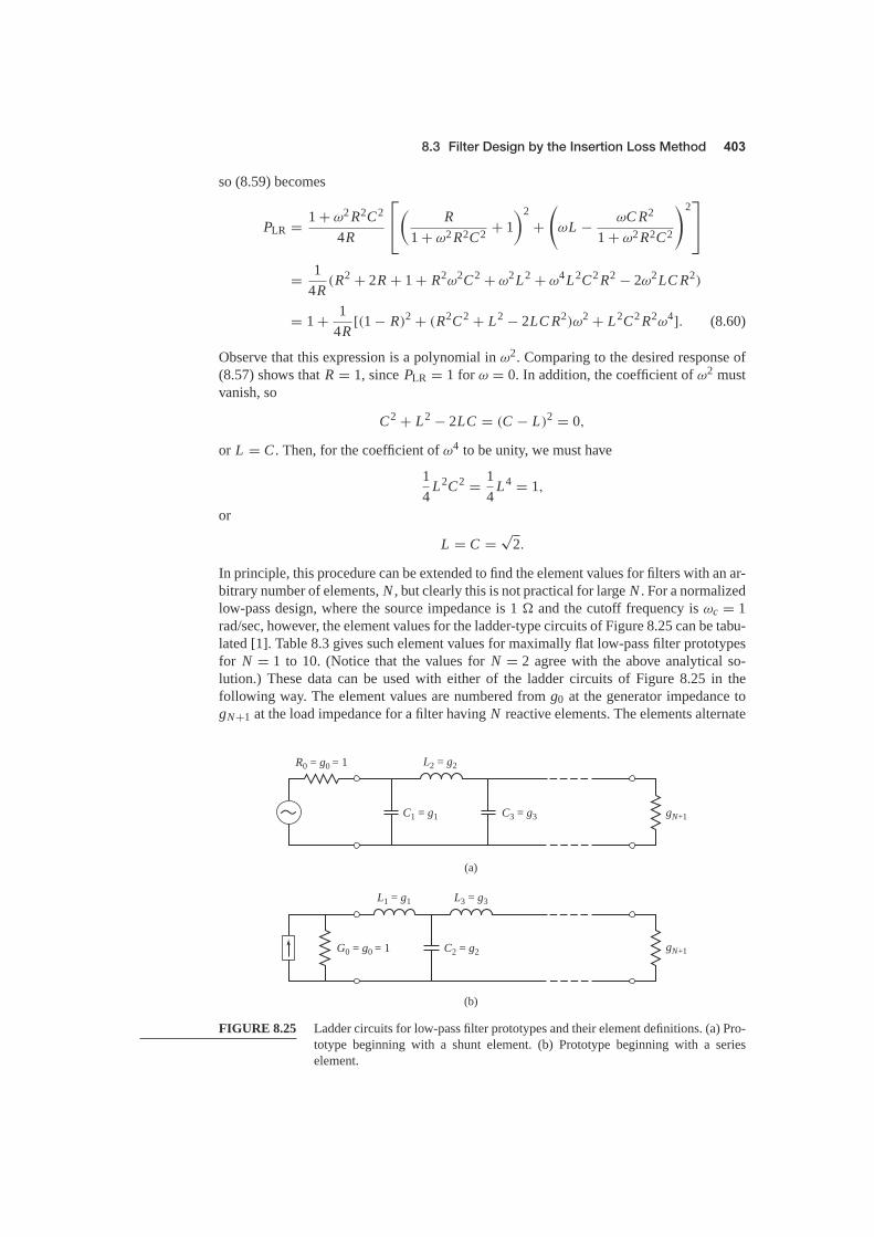
8.3 Filter Design by the Insertion Loss Method
so (8.59) becomes
PLR = 1 + ω2 R2C2
4R
⎡⎣(
R1 + ω2 R2C2 + 1
)2+
(ωL − ωC R2
1 + ω2 R2C2
)2⎤⎦
= 14R
(R2 + 2R + 1 + R2ω2C2 + ω2L2 + ω4L2C2 R2 − 2ω2LC R2)
= 1 + 14R
[(1 − R)2 + (R2C2 + L2 − 2LC R2)ω2 + L2C2 R2ω4]. (8.60)
Observe that this expression is a polynomial in ω2. Comparing to the desired response of(8.57) shows that R = 1, since PLR = 1 for ω = 0. In addition, the coefficient of ω2 mustvanish, so
C2 + L2 − 2LC = (C − L)2 = 0,
or L = C . Then, for the coefficient of ω4 to be unity, we must have
14
L2C2 = 14
L4 = 1,
or
L = C = √2.
In principle, this procedure can be extended to find the element values for filters with an ar-bitrary number of elements, N , but clearly this is not practical for large N . For a normalizedlow-pass design, where the source impedance is 1 � and the cutoff frequency is ωc = 1rad/sec, however, the element values for the ladder-type circuits of Figure 8.25 can be tabu-lated [1]. Table 8.3 gives such element values for maximally flat low-pass filter prototypesfor N = 1 to 10. (Notice that the values for N = 2 agree with the above analytical so-lution.) These data can be used with either of the ladder circuits of Figure 8.25 in thefollowing way. The element values are numbered from g0 at the generator impedance togN+1 at the load impedance for a filter having N reactive elements. The elements alternate
C3 = g3C1 = g1
C2 = g2G0 = g0 = 1
R0 = g0 = 1
L3 = g3L1 = g1
L2 = g2
gN+1
gN+1
(a)
(b)
FIGURE 8.25 Ladder circuits for low-pass filter prototypes and their element definitions. (a) Pro-totype beginning with a shunt element. (b) Prototype beginning with a serieselement.

Chapter 8: Microwave Filters
TABLE 8.3 Element Values for Maximally Flat Low-Pass Filter Prototypes (g0 = 1,
ωc = 1, N = 1 to 10)
N g1 g2 g3 g4 g5 g6 g7 g8 g9 g10 g11
1 2.0000 1.00002 1.4142 1.4142 1.00003 1.0000 2.0000 1.0000 1.00004 0.7654 1.8478 1.8478 0.7654 1.00005 0.6180 1.6180 2.0000 1.6180 0.6180 1.00006 0.5176 1.4142 1.9318 1.9318 1.4142 0.5176 1.00007 0.4450 1.2470 1.8019 2.0000 1.8019 1.2470 0.4450 1.00008 0.3902 1.1111 1.6629 1.9615 1.9615 1.6629 1.1111 0.3902 1.00009 0.3473 1.0000 1.5321 1.8794 2.0000 1.8794 1.5321 1.0000 0.3473 1.0000
10 0.3129 0.9080 1.4142 1.7820 1.9754 1.9754 1.7820 1.4142 0.9080 0.3129 1.0000
Source: Reprinted from G. L. Matthaei, L. Young, and E. M. T. Jones, Microwave Filters, Impedance-MatchingNetworks, and Coupling Structures, Artech House, Dedham, Mass., 1980, with permission.
between series and shunt connections, and gk has the following definition:
g0 ={
generator resistance (network of Figure 8.25a)generator conductance (network of Figure 8.25b)
gk(k = 1 to N )
={
inductance for series inductorscapacitance for shunt capacitors
gN+1 ={
load resistance if gN is a shunt capacitorload conductance if gN is a series inductor
Then the circuits of Figure 8.25 can be considered as the dual of each other, and both willgive the same filter response.
Finally, as a matter of practical design procedure, it will be necessary to determine thesize, or order, of the filter. This is usually dictated by a specification on the insertion lossat some frequency in the stopband of the filter. Figure 8.26 shows the attenuation charac-teristics for various N versus normalized frequency. If a filter with N > 10 is required, agood result can usually be obtained by cascading two designs of lower order.
For an equal-ripple low-pass filter with a cutoff frequency ωc = 1 rad/sec, the power lossratio from (8.54) is
PLR = 1 + k2T 2N (ω), (8.61)
where 1 + k2 is the ripple level in the passband. Since the Chebyshev polynomials havethe property that
TN (0) ={
0 for N odd,1 for N even,
equation (8.61) shows that the filter will have a unity power loss ratio at ω = 0 for N odd,but a power loss ratio of 1 + k2 at ω = 0 for N even. Thus, there are two cases to consider,depending on N.
8.3 Filter Design by the Insertion Loss Method
0.1 0.2 0.3 0.5 0.7 1.0 2.0 3.0 5.0 7.0 100
10
20
30
40
50
60
70
Atte
nuat
ion
(dB
)
c
– 1
n = 1
n = 4n = 5
n = 2n = 3
n = 7n = 6
n = 8n = 9
n = 10
FIGURE 8.26 Attenuation versus normalized frequency for maximally flat filter prototypes.Adapted from G. L. Matthaei, L. Young, and E. M. T. Jones, Microwave Filters, Impedance-Matching Networks, and Coupling Structures, Artech House, Dedham, Mass., 1980, withpermission.
For the two-element filter of Figure 8.24, the power loss ratio is given in terms of thecomponent values in (8.60). From (5.56b), we see that T2(x) = 2x2 − 1, so equating (8.61)to (8.60) gives
1+ k2(4ω4 − 4ω2 + 1)=1 + 14R
[(1 − R)2 + (R2C2+ L2 − 2LC R2) ω2+ L2C2 R2ω4],(8.62)
which can be solved for R, L , and C if the ripple level (as determined by k2) is known.Thus, at ω = 0 we have that
k2 = (1 − R)2
4R,
or
R = 1 + 2k2 ± 2k√
1 + k2 (for N even). (8.63)
Equating coefficients of ω2 and ω4 yields the additional relations
4k2 = 14R
L2C2 R2,
−4k2 = 14R
(R2C2 + L2 − 2LC R2),
which can be used to find L and C . Note that (8.63) gives a value for R that is not unity, sothere will be an impedance mismatch if the load has a unity (normalized) impedance; this

Chapter 8: Microwave Filters
TABLE 8.4 Element Values for Equal-Ripple Low-Pass Filter Prototypes (g0 = 1, ωc =1, N = 1 to 10, 0.5 dB and 3.0 dB ripple)
0.5 dB RippleN g1 g2 g3 g4 g5 g6 g7 g8 g9 g10 g11
1 0.6986 1.00002 1.4029 0.7071 1.98413 1.5963 1.0967 1.5963 1.00004 1.6703 1.1926 2.3661 0.8419 1.98415 1.7058 1.2296 2.5408 1.2296 1.7058 1.00006 1.7254 1.2479 2.6064 1.3137 2.4758 0.8696 1.98417 1.7372 1.2583 2.6381 1.3444 2.6381 1.2583 1.7372 1.00008 1.7451 1.2647 2.6564 1.3590 2.6964 1.3389 2.5093 0.8796 1.98419 1.7504 1.2690 2.6678 1.3673 2.7239 1.3673 2.6678 1.2690 1.7504 1.0000
10 1.7543 1.2721 2.6754 1.3725 2.7392 1.3806 2.7231 1.3485 2.5239 0.8842 1.9841
3.0 dB RippleN g1 g2 g3 g4 g5 g6 g7 g8 g9 g10 g11
1 1.9953 1.00002 3.1013 0.5339 5.80953 3.3487 0.7117 3.3487 1.00004 3.4389 0.7483 4.3471 0.5920 5.80955 3.4817 0.7618 4.5381 0.7618 3.4817 1.00006 3.5045 0.7685 4.6061 0.7929 4.4641 0.6033 5.80957 3.5182 0.7723 4.6386 0.8039 4.6386 0.7723 3.5182 1.00008 3.5277 0.7745 4.6575 0.8089 4.6990 0.8018 4.4990 0.6073 5.80959 3.5340 0.7760 4.6692 0.8118 4.7272 0.8118 4.6692 0.7760 3.5340 1.0000
10 3.5384 0.7771 4.6768 0.8136 4.7425 0.8164 4.7260 0.8051 4.5142 0.6091 5.8095
Source: Reprinted from G. L. Matthaei, L. Young, and E. M. T. Jones, Microwave Filters, Impedance-MatchingNetworks, and Coupling Structures, Artech House, Dedham, Mass.,1980, with permission.
can be corrected with a quarter-wave transformer, or by using an additional filter elementto make N odd. For odd N , it can be shown that R = 1. (This is because there is a unitypower loss ratio at ω = 0 for N odd.)
Tables exist for designing equal-ripple low-pass filters with a normalized source im-pedance and cutoff frequency (ω′
c = 1 rad/sec) [1], and these can be applied to either ofthe ladder circuits of Figure 8.25. This design data depends on the specified passband ripplelevel; Table 8.4 lists element values for normalized low-pass filter prototypes having 0.5 or3.0 dB ripple for N = 1 to 10. Notice that the load impedance gN+1 �= 1 for even N . If thestopband attenuation is specified, the curves in Figure 8.27 can be used to determine thenecessary value of N for these ripple values.
Filters having a maximally flat time delay, or a linear phase response, can be designed inthe same way, but things are somewhat more complicated because the phase of the volt-age transfer function is not as simply expressed as is its amplitude. Design values have

8.3 Filter Design by the Insertion Loss Method
0.01 0.02 0.03 0.05 0.07 0.10 0.20 0.30 0.50 0.70 1.0 2.0 3.0 5.0 7.0 10.00
10
20
30
40
50
60
70
Atte
nuat
ion
(dB
)
c
– 1
n = 1
n = 2
n = 3
n = 7
n = 6
n = 8
n = 9
n = 1
0
(b)
0.01 0.02 0.03 0.05 0.07 0.10 0.20 0.30 0.50 0.70 1.0 2.0 3.0 5.0 7.0 10.00
10
20
30
40
50
60
70
Atte
nuat
ion
(dB
)
c
– 1
n = 2
n = 3
n = 7
n = 6n =
8
n = 9
n = 1
0
(a)n = 5
n = 4
n = 1
n = 5n = 4
FIGURE 8.27 Attenuation versus normalized frequency for equal-ripple filter prototypes.(a) 0.5 dB ripple level. (b) 3.0 dB ripple level.Adapted from G. L. Matthaei, L. Young, and E. M. T. Jones, Microwave Filters, Impedance-Matching Networks, and Coupling Structures, Artech House, Dedham, Mass., 1980, withpermission.

Chapter 8: Microwave Filters
TABLE 8.5 Element Values for Maximally Flat Time Delay Low-Pass Filter Prototypes(g0 = 1, ωc = 1, N = 1 to 10)
N g1 g2 g3 g4 g5 g6 g7 g8 g9 g10 g11
1 2.0000 1.00002 1.5774 0.4226 1.00003 1.2550 0.5528 0.1922 1.00004 1.0598 0.5116 0.3181 0.1104 1.00005 0.9303 0.4577 0.3312 0.2090 0.0718 1.00006 0.8377 0.4116 0.3158 0.2364 0.1480 0.0505 1.00007 0.7677 0.3744 0.2944 0.2378 0.1778 0.1104 0.0375 1.00008 0.7125 0.3446 0.2735 0.2297 0.1867 0.1387 0.0855 0.0289 1.00009 0.6678 0.3203 0.2547 0.2184 0.1859 0.1506 0.1111 0.0682 0.0230 1.0000
10 0.6305 0.3002 0.2384 0.2066 0.1808 0.1539 0.1240 0.0911 0.0557 0.0187 1.0000
Source: Reprinted from G. L. Matthaei, L. Young, and E. M. T. Jones, Microwave Filters, Impedance-MatchingNetworks, and Coupling Structures, Artech House, Dedham, Mass., 1980, with permission.
been derived for such filters [1], however, again for the ladder circuits of Figure 8.25, andthey are given in Table 8.5 for a normalized source impedance and cutoff frequency(ω′
c = 1 rad/sec). The resulting normalized group delay in the passband will be τd =1/ω′
c = 1 sec.
The low-pass filter prototypes of the previous section were normalized designs having asource impedance of Rs = 1 � and a cutoff frequency of ωc = 1 rad/sec. Here we showhow these designs can be scaled in terms of impedance and frequency, and converted togive high-pass, bandpass, or bandstop characteristics. Several examples will be presentedto illustrate the design procedure.
Impedance scaling: In the prototype design, the source and load resistances are unity (ex-cept for equal-ripple filters with even N , which have nonunity load resistance). A sourceresistance of R0 can be obtained by multiplying all the impedances of the prototype designby R0. Thus, if we let primes denote impedance scaled quantities, the new filter componentvalues are given by
L ′ = R0L , (8.64a)
C ′ = CR0
, (8.64b)
R′s = R0, (8.64c)
R′L = R0 RL , (8.64d)
where L , C , and RL are the component values for the original prototype.

8.4 Filter Transformations
Frequency scaling for low-pass filters: To change the cutoff frequency of a low-pass pro-totype from unity to ωc requires that we scale the frequency dependence of the filter by thefactor 1/ωc, which is accomplished by replacing ω by ω/ωc:
ω ← ω
ωc. (8.65)
Then the new power loss ratio will be
P ′LR(ω) = PLR
(ω
ωc
),
where ωc is the new cutoff frequency; cutoff occurs when ω/ωc = 1, or ω = ωc. Thistransformation can be viewed as a stretching, or expansion, of the original passband, asillustrated in Figure 8.28a, b.
The new element values are determined by applying the substitution of (8.65) to theseries reactances, jωLk , and shunt susceptances, jωCk , of the prototype filter. Thus,
j Xk = jω
ωcLk = jωL ′
k,
j Bk = jω
ωcCk = jωC ′
k,
which shows that the new element values are given by
L ′k = Lk
ωc, (8.66a)
C ′k = Ck
ωc. (8.66b)
When both impedance and frequency scaling are required, the results of (8.64) can becombined with (8.66) to give
L ′k = R0Lk
ωc, (8.67a)
C ′k = Ck
R0ωc. (8.67b)
PLR
0–1 1
(a)
PLR
0–c c
(b)
PLR
0–c c
(c)
FIGURE 8.28 Frequency scaling for low-pass filters and transformation to a high-pass response.(a) Low-pass filter prototype response for ωc = 1 rad/sec. (b) Frequency scalingfor low-pass response. (c) Transformation to high-pass response.

Chapter 8: Microwave Filters
Low-pass to high-pass transformation: The frequency substitution
ω ← −ωc
ω(8.68)
can be used to convert a low-pass response to a high-pass response, as shown inFigure 8.28c. This substitution maps ω = 0 to ω = ±∞, and vice versa; cutoff occurswhen ω = ±ωc. The negative sign is needed to convert inductors (and capacitors) to real-izable capacitors (and inductors). Applying (8.68) to the series reactances, jωLk , and theshunt susceptances, jωCk , of the prototype filter gives
j Xk = − jωc
ωLk = 1
jωC ′k,
j Bk = − jωc
ωCk = 1
jωL ′k,
which shows that series inductors Lk must be replaced with capacitors C ′k , and shunt ca-
pacitors Ck must be replaced with inductors L ′k . The new component values are given by
C ′k = 1
ωc Lk, (8.69a)
L ′k = 1
ωcCk. (8.69b)
Impedance scaling can be included by using (8.64) to give
C ′k = 1
R0ωc Lk, (8.70a)
L ′k = R0
ωcCk. (8.70b)
EXAMPLE 8.3 LOW-PASS FILTER DESIGN COMPARISON
Design a maximally flat low-pass filter with a cutoff frequency of 2 GHz, imped-ance of 50 �, and at least 15 dB insertion loss at 3 GHz. Compute and plot theamplitude response and group delay for f = 0 to 4 GHz, and compare with anequal-ripple (3.0 dB ripple) and linear phase filter having the same order.
SolutionFirst find the required order of the maximally flat filter to satisfy the insertion lossspecification at 3 GHz. We have that |ω/ωc| − 1 = 0.5; from Figure 8.26 we seethat N = 5 will be sufficient. Then Table 8.3 gives the prototype element values as
g1 = 0.618,
g2 = 1.618,
g3 = 2.000,
g4 = 1.618,
g5 = 0.618.

8.4 Filter Transformations
RS = 50 Ω L2' L4'
C1' C3' C5' RL = 50 Ω
FIGURE 8.29 Low-pass, maximally flat filter circuit for Example 8.3.
Then (8.67) can be used to obtain the scaled element values:
C ′1 = 0.984 pF,
L ′2 = 6.438 nH,
C ′3 = 3.183 pF,
L ′4 = 6.438 nH,
C ′5 = 0.984 pF.
The final filter circuit is shown in Figure 8.29; the ladder circuit of Figure 8.25awas used, but that of Figure 8.25b could have been used just as well.
The component values for the equal-ripple filter and the linear phase filter,for N = 5, can be determined from Tables 8.4 and 8.5. The amplitude and groupdelay results for these three filters are shown in Figure 8.30. These results clearlyshow the trade-offs involved with the three types of filters. The equal-ripple re-sponse has the sharpest cutoff but the worst group delay characteristics. The max-imally flat response has a flatter attenuation characteristic in the passband but aslightly lower cutoff rate. The linear phase filter has the worst cutoff rate but avery good group delay characteristic. ■
Low-pass prototype filter designs can also be transformed to have the bandpass or bandstopresponses illustrated in Figure 8.31. If ω1 and ω2 denote the edges of the passband, then abandpass response can be obtained using the following frequency substitution:
ω ← ω0
ω2 − ω1
(ω
ω0− ω0
ω
)= 1
�
(ω
ω0− ω0
ω
), (8.71)
where
� = ω2 − ω1
ω0(8.72)
is the fractional bandwidth of the passband. The center frequency, ω0, could be chosenas the arithmetic mean of ω1 and ω2, but the equations are simpler if it is chosen as thegeometric mean:
ω0 = √ω1ω2. (8.73)
Then the transformation of (8.71) maps the bandpass characteristics of Figure 8.31b to the

Chapter 8: Microwave Filters
40
30
20
10
0
0 1.0 2.0 3.0 4.00
0.25
0.5
0.75
1.0
1.25
1.5
Frequency (GHz)
0 1.0 2.0 3.0 4.0Frequency (GHz)
(b)
(a)
Gro
up d
elay
(nse
c)A
ttenu
atio
n (d
B)
Equal-rippleN = 5
Linear phaseN = 5
Maximally flatN = 5
Equal-ripple
Linear phase
Maximally flat
FIGURE 8.30 Frequency response of the filter design of Example 8.3. (a) Amplitude response.(b) Group delay response.
FIGURE 8.31 Bandpass and bandstop frequency transformations. (a) Low-pass filter prototyperesponse for ωc = 1. (b) Transformation to bandpass response. (c) Transformationto bandstop response.

8.4 Filter Transformations
low-pass response of Figure 8.31a as follows:
When ω = ω0,1�
(ω
ω0− ω0
ω
)= 0.
When ω = ω1,1�
(ω
ω0− ω0
ω
)= 1
�
(ω2
1 − ω20
ω0ω1
)= −1.
When ω = ω2,1�
(ω
ω0− ω0
ω
)= 1
�
(ω2
2 − ω20
ω0ω2
)= 1.
The new filter elements are determined by using (8.71) in the expressions for the seriesreactance and shunt susceptances. Thus,
j Xk = j�
(ω
ω0− ω0
ω
)Lk = j
ωLk
�ω0− j
ω0Lk
�ω= jωL ′
k − j1
ωC ′k,
which shows that a series inductor, Lk , is transformed to a series LC circuit with elementvalues
L ′k = Lk
�ω0, (8.74a)
C ′k = �
ω0Lk. (8.74b)
Similarly,
j Bk = j�
(ω
ω0− ω0
ω
)Ck = j
ωCk
�ω0− j
ω0Ck
�ω= jωC ′
k − j1
ωL ′k,
which shows that a shunt capacitor, Ck , is transformed to a shunt LC circuit with elementvalues
L ′k = �
ω0Ck, (8.74c)
C ′k = Ck
�ω0. (8.74d)
The low-pass filter elements are thus converted to series resonant circuits (having a lowimpedance at resonance) in the series arms, and to parallel resonant circuits (having a highimpedance at resonance) in the shunt arms. Notice that both series and parallel resonatorelements have a resonant frequency of ω0.
The inverse transformation can be used to obtain a bandstop response. Thus,
ω ← −�
(ω
ω0− ω0
ω
)−1, (8.75)
where � and ω0 have the same definitions as in (8.72) and (8.73). Then series inductors ofthe low-pass prototype are converted to parallel LC circuits having element values given by
L ′k = �Lk
ω0, (8.76a)
C ′k = 1
ω0�Lk. (8.76b)

Chapter 8: Microwave Filters
TABLE 8.6 Summary of Prototype Filter Transformations(
� = ω2 − ω1ω0
)
Low-pass High-pass Bandpass Bandstop
C
L
1cC
1cL
Δ0C
C0Δ
10CΔ
CΔ0
Δ0L
L0Δ 1
0LΔLΔ
0
The shunt capacitor of the low-pass prototype is converted to series LC circuits havingelement values given by
L ′k = 1
ω0�Ck, (8.76c)
C ′k = �Ck
ω0. (8.76d)
The element transformations from a low-pass prototype to a high-pass, bandpass, orbandstop filter are summarized in Table 8.6. These results do not include impedance scal-ing, which can be made using (8.64).
EXAMPLE 8.4 BANDPASS FILTER DESIGN
Design a bandpass filter having a 0.5 dB equal-ripple response, with N = 3.The center frequency is 1 GHz, the bandwidth is 10%, and the impedanceis 50 �.
50 Ω
L2' C 2'
L3'C1'L 1' C3'
50 Ω
FIGURE 8.32 Bandpass filter circuit for Example 8.4.

8.5 Filter Implementation
0.5 0.75 1.0 1.25 1.550
40
30
20
10
0
Atte
nuat
ion
(dB
)
Frequency (GHz)
FIGURE 8.33 Amplitude response for the bandpass filter of Example 8.4.
SolutionFrom Table 8.4 the element values for the low-pass prototype circuit of Figure8.25b are given as
g1 = 1.5963 = L1,
g2 = 1.0967 = C2,
g3 = 1.5963 = L3,
g4 = 1.000 = RL .
Equations (8.64) and (8.74) give the impedance-scaled and frequency-transformedelement values for the circuit of Figure 8.32 as
L ′1 = L1 R0
ω0�= 127.0 nH,
C ′1 = �
ω0L1 R0= 0.199 pF,
L ′2 = �R0
ω0C2= 0.726 nH,
C ′2 = C2
ω0�R0= 34.91 pF,
L ′3 = L3 R0
ω0�= 127.0 nH,
C ′3 = �
ω0L3 R0= 0.199 pF.
The resulting amplitude response is shown in Figure 8.33. ■
The lumped-element filter designs discussed in the previous sections generally work wellat low frequencies, but two problems arise at higher RF and microwave frequencies. First,lumped-element inductors and capacitors are generally available only for a limited range ofvalues, and can be difficult to implement at microwave frequencies. Distributed elements,
Chapter 8: Microwave Filters
such as open-circuited or short-circuited transmission line stubs, are often used to approx-imate ideal lumped elements. In addition, at microwave frequencies the distances betweenfilter components is not negligible. The first problem is treated with Richards’ transforma-tion, which can be used to convert lumped elements to transmission line sections. Kuroda’sidentities can then be used to physically separate filter elements by using transmissionline sections. Because such additional transmission line sections do not affect the filterresponse, this type of design is called redundant filter synthesis. It is possible to designmicrowave filters that take advantage of these sections to improve the filter response [4];such nonredundant synthesis does not have a lumped-element counterpart.
The transformation
� = tan β� = tan(
ω�
vp
)(8.77)
maps the ω plane to the � plane, which repeats with a period of ω�/vp = 2π . This trans-formation was introduced by P. Richards [6] to synthesize an LC network using open- andshort-circuited transmission line stubs. Thus, if we replace the frequency variable ω with�, we can write the reactance of an inductor as
j X L = j�L = j L tan β�, (8.78a)
and the susceptance of a capacitor as
j BC = j�C = jC tan β�. (8.78b)
These results indicate that an inductor can be replaced with a short-circuited stub of lengthβ� and characteristic impedance L ,while a capacitor can be replaced with an open-circuitedstub of length β� and characteristic impedance 1/C . A unity filter impedance is assumed.
Cutoff occurs at unity frequency for a low-pass filter prototype; to obtain the samecutoff frequency for the Richards’-transformed filter, (8.77) shows that
� = 1 = tan β�,
which gives a stub length of � = λ/8, where λ is the wavelength of the line at the cutofffrequency, ωc. At the frequency ω0 = 2ωc, the lines will be λ/4 long, and an attenuationpole will occur. At frequencies away from ωc, the impedances of the stubs will no longermatch the original lumped-element impedances, and the filter response will differ fromthe desired prototype response. In addition, the response will be periodic in frequency,repeating every 4ωc.
In principle, then, Richards’ transformation allows the inductors and capacitors of alumped-element filter to be replaced with short-circuited and open-circuited transmissionline stubs, as illustrated in Figure 8.34. Since the electrical lengths of all the stubs are thesame (λ/8 at ωc), these lines are called commensurate lines.
The four Kuroda identities use redundant transmission line sections to achieve a morepractical microwave filter implementation by performing any of the following operations:
� Physically separate transmission line stubs� Transform series stubs into shunt stubs, or vice versa� Change impractical characteristic impedances into more realizable values

8.5 Filter Implementation
jXLjXL
Z0 = L
�/8 at c
S.C.
jBc
Z0 =
jBc
�/8 at c
O.C.
1C
L
C
(a)
(b)
FIGURE 8.34 Richards’ transformation. (a) For an inductor to a short-circuited stub. (b) For acapacitor to an open-circuited stub.
The additional transmission line sections are called unit elements and are λ/8 long at ωc;the unit elements are thus commensurate with the stubs used to implement the inductorsand capacitors of the prototype design.
The four Kuroda identities are illustrated in Table 8.7, where each box represents aunit element, or transmission line, of the indicated characteristic impedance and length(λ/8 at ωc). The inductors and capacitors represent short-circuit and open-circuit stubs,
TABLE 8.7 The Four Kuroda Identities (n2 = 1 + Z2/Z1)
Z1
n2
Z1
n2
Z2
n2
Z2
n2
n2Z 2n2Z 1
1 : n2
n2 : 1
1
Z 2
1
Z 2
1n2Z 2
n2Z 1Z 1
Z 2
Z 2
Z 1
Z 1
Z 1
1
≡
(a)
≡
(b)
≡
(c)
≡
(d)

Chapter 8: Microwave Filters
l l
l
l
O.C.shuntstub
Unitelement
Z1
Z2
≡ Z2/n2
Z1/n2
Unitelement
n2 = 1 + Z2/Z1
S.C.seriesstub
FIGURE 8.35 Equivalent circuits illustrating Kuroda identity (a) in Table 8.7.
respectively. We will prove the equivalence of the first case, and then show how to usethese identities in Example 8.5.
The two circuits of identity (a) in Table 8.7 can be redrawn as shown in Figure 8.35;we will show that these two networks are equivalent by showing that their ABCD matricesare identical. From Table 4.1, the ABCD matrix of a length � of transmission line withcharacteristic impedance Z1 is
[A BC D
]=
[ cos β� j Z1 sin β�
jZ1
sin β� cos β�
]= 1√
1 + �2
[ 1 j�Z1j�Z1
1
], (8.79)
where � = tan β�. The open-circuited shunt stub in the first circuit in Figure 8.35 has animpedance of − j Z2 cot β� = − j Z2/�, so the ABCD matrix of the entire circuit is
[A BC D
]L
=⎡⎣ 1 0
j�Z2
1
⎤⎦⎡⎣ 1 j�Z1
j�Z1
1
⎤⎦ 1√
1 + �2
= 1√1 + �2
⎡⎣ 1 j�Z1
j�(
1Z1
+ 1Z2
)1 − �2 Z1
Z2
⎤⎦. (8.80a)
The short-circuited series stub in the second circuit in Figure 8.35 has an impedanceof j (Z1/n2) tan β� = j�Z1/n2, so the ABCD matrix of the entire circuit is
[A BC D
]R
=⎡⎢⎣ 1 j
�Z2
n2
j�n2
Z21
⎤⎥⎦⎡⎣ 1
j�Z1
n2
0 1
⎤⎦ 1√
1 + �2
= 1√1 + �2
⎡⎢⎣ 1
j�n2 (Z1 + Z2)
j�n2
Z21 − �2 Z1
Z2
⎤⎥⎦. (8.80b)
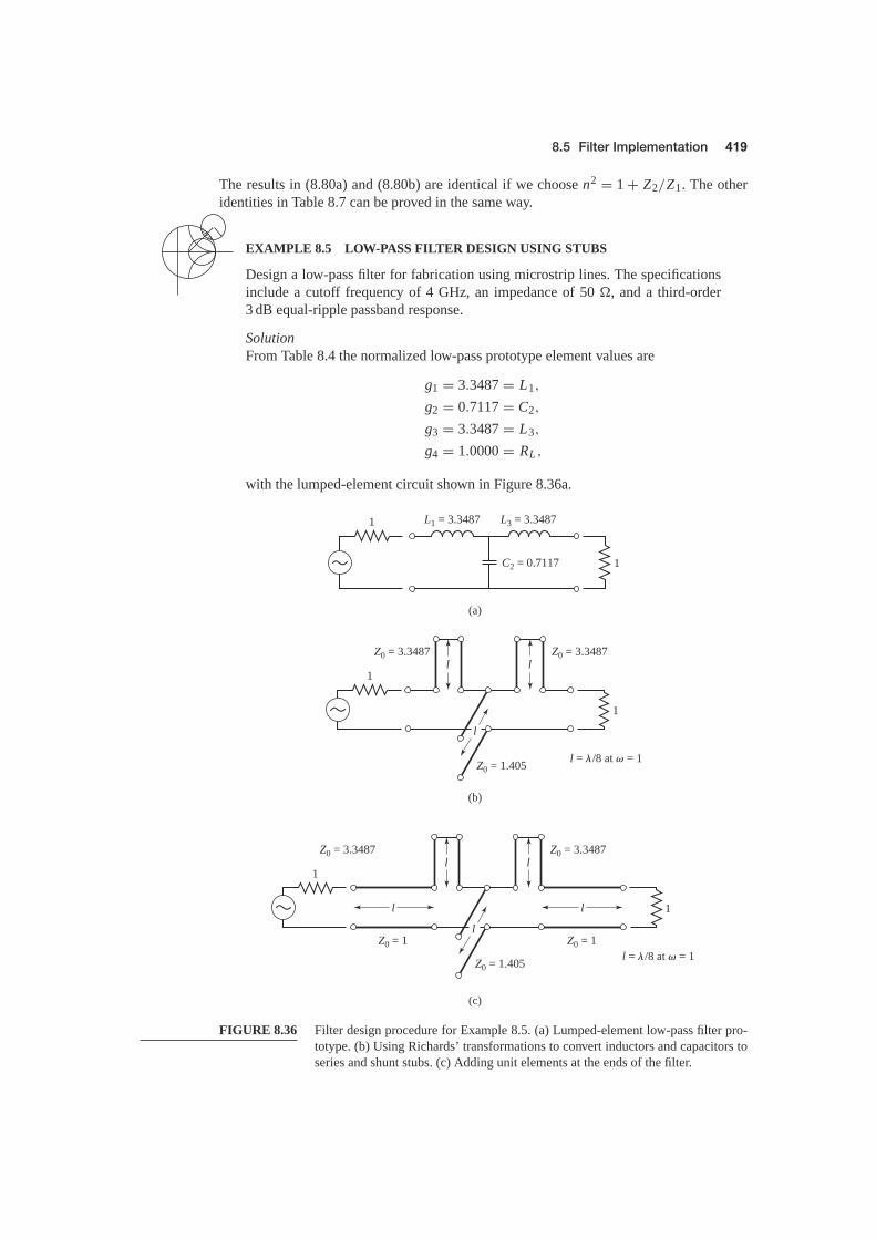
8.5 Filter Implementation
The results in (8.80a) and (8.80b) are identical if we choose n2 = 1 + Z2/Z1. The otheridentities in Table 8.7 can be proved in the same way.
EXAMPLE 8.5 LOW-PASS FILTER DESIGN USING STUBS
Design a low-pass filter for fabrication using microstrip lines. The specificationsinclude a cutoff frequency of 4 GHz, an impedance of 50 �, and a third-order3 dB equal-ripple passband response.
SolutionFrom Table 8.4 the normalized low-pass prototype element values are
g1 = 3.3487 = L1,
g2 = 0.7117 = C2,
g3 = 3.3487 = L3,
g4 = 1.0000 = RL ,
with the lumped-element circuit shown in Figure 8.36a.
1
1
1
1
L1 = 3.3487
Z0 = 3.3487 Z0 = 3.3487
Z0 = 1.405
L3 = 3.3487
C2 = 0.7117
(a)
(b)
(c)
l = �/8 at = 1
l l
l
1
1
Z0 = 3.3487 Z0 = 3.3487
Z0 = 1.405
Z0 = 1 Z0 = 1l = �/8 at = 1
l
l l
l
l
FIGURE 8.36 Filter design procedure for Example 8.5. (a) Lumped-element low-pass filter pro-totype. (b) Using Richards’ transformations to convert inductors and capacitors toseries and shunt stubs. (c) Adding unit elements at the ends of the filter.

Chapter 8: Microwave Filters
Z0 = 217.5 Ω Z0 = 217.5 Ω
Z0 =64.9 Ω
Z0 =70.3 Ω
Z0 =64.9 Ω
(e)
(f)
l = �/8 at 4 GHz
l l
l l
l
50 Ω217.5 Ω 217.5 Ω
50 Ω
50 Ω
50 Ω
Z0 = 4.350 Z0 = 4.350
Z0 =1.299
Z0 =1.405
Z0 =1.299
(d)l = �/8 at = 1
l l
l l
l
1
1
64.9 Ω 70.3 Ω 64.9 Ω
FIGURE 8.36 Continued. (d) Applying the second Kuroda identity. (e) After impedance and fre-quency scaling. (f) Microstrip fabrication of the final filter.
We now use Richards’ transformations to convert series inductors to seriesstubs, and shunt capacitors to shunt stubs, as shown in Figure 8.36b. Accordingto (8.78), the characteristic impedance of a series stub (inductor) is L , and thecharacteristic impedance of a shunt stub (capacitor) is 1/C . For commensurateline synthesis, all stubs are λ/8 long at ω = ωc. (It is usually most convenient towork with normalized quantities until the last step in the design.)
The series stubs of Figure 8.36b would be very difficult to implement in mi-crostrip line form, so we will use one of the Kuroda identities to convert theseto shunt stubs. First we add unit elements at either end of the filter, as shownin Figure 8.36c. These redundant elements do not affect filter performance sincethey are matched to the source and load (Z0 = 1). Then we can apply Kurodaidentity (b) from Table 8.7 to both ends of the filter. In both cases we have that
n2 = 1 + Z2
Z1= 1 + 1
3.3487= 1.299.
The result is shown in Figure 8.36d.Finally, we impedance and frequency scale the circuit, which simply involves
multiplying the normalized characteristic impedances by 50 � and choosing theline and stub lengths to be λ/8 at 4 GHz. The final circuit is shown in Figure 8.36e,with a microstrip layout in Figure 8.36f.

8.5 Filter Implementation
0 5 10 15 2050
40
30
20
10
0
Frequency (GHz)
Atte
nuat
ion
(dB
)
Lumpedelements
Distributedelements
FIGURE 8.37 Amplitude responses of lumped-element and distributed-element low-pass filter ofExample 8.5.
The calculated amplitude response of this filter is plotted in Figure 8.37,along with the response of the lumped-element version. Note that the pass-band characteristics are very similar up to 4 GHz, but the distributed-elementfilter has a sharper cutoff. Also notice that the distributed-element filter has a re-sponse that repeats every 16 GHz, as a result of the periodic nature of Richards’transformation. ■
Similar procedures can be used for bandstop filters, but the Kuroda identities are notuseful for high-pass or bandpass filters.
As we have seen, it is often desirable to use only series, or only shunt, elements whenimplementing a filter with a particular type of transmission line. The Kuroda identitiescan be used for conversions of this form, but another possibility is to use impedance (K )or admittance (J ) inverters [1, 4, 7]. Such inverters are especially useful for bandpass orbandstop filters with narrow (<10%) bandwidths.
The conceptual operation of impedance and admittance inverters is illustrated inFigure 8.38; since these inverters essentially form the inverse of the load impedance oradmittance, they can be used to transform series-connected elements to shunt-connectedelements, or vice versa. This procedure will be illustrated in later sections for bandpassand bandstop filters.
In its simplest form, an impedance or admittance inverter can be constructed using aquarter-wave transformer of the appropriate characteristic impedance, as shown in Figure8.38b. This implementation also allows the ABCD matrix of the inverter to be easily foundfrom the ABCD parameters for a length of transmission line, as given in Table 4.1. Manyother types of circuits can also be used as impedance or admittance inverters, with one suchalternative being shown in Figure 8.38c. Inverters of this form turn out to be useful formodeling the coupled resonator filters of Section 8.8. The lengths, θ/2, of the transmissionline sections are generally required to be negative for this type of inverter, but this poses noproblem if these lines can be absorbed into connecting transmission lines on either side.

Chapter 8: Microwave Filters
�/4
�/2 �/2
Zin = K 2/ZL
Z0 = K
Z0 Z0jX
K± 90°
ZL
K = Z0 tan ⎜�/2⎜
X = K1 – (K/Z0)2
� = –tan–1 2XZ0
(c)
(b)
(a)
Impedance inverters
�/4
�/2 �/2
Yin = J 2/YL
Y0 = J
Y0 Y0jB
J± 90°
J = Y0 tan ⎜�/2⎜
B = J1 – (J/Y0)2
� = –tan–1 2BY0
Admittance inverters
YL
�C
K = 1/C
�C
C �C
J = C
�C
C
(d)
FIGURE 8.38 Impedance and admittance inverters. (a) Operation of impedance and admittanceinverters. (b) Implementation as quarter-wave transformers. (c) Implementationusing transmission lines and reactive elements. (d) Implementation using capacitornetworks.
A relatively easy way to implement low-pass filters in microstrip or stripline is to use alter-nating sections of very high and very low characteristic impedance lines. Such filters areusually referred to as stepped-impedance, or hi-Z , low-Z filters, and are popular becausethey are easier to design and take up less space than a similar low-pass filter using stubs.Because of the approximations involved, however, their electrical performance is not asgood, so the use of such filters is usually limited to applications where a sharp cutoff is notrequired (for instance, in rejecting out-of-band mixer products).
We begin by finding the approximate equivalent circuits for a short length of transmis-sion line having either a very large or a very small characteristic impedance. The ABCD

8.6 Stepped-Impedance Low-Pass Filters
X = Z0�l
B = Y0�l
jB
j X2
j X2
(a) (b)
(c)
FIGURE 8.39 Approximate equivalent circuits for short sections of transmission lines. (a) T-equivalent circuit for a transmission line section having β� π/2. (b) Equivalentcircuit for small β� and large Z0. (c) Equivalent circuit for small β� and small Z0.
parameters of a length � of line having characteristic impedance Z0 are given in Table 4.1;the conversion in Table 4.2 can then be used to find the impedance parameters as
Z11 = Z22 = AC
= − j Z0 cot β�, (8.81a)
Z12 = Z21 = 1C
= − j Z0 csc β�. (8.81b)
The series elements of the T-equivalent circuit are
Z11 − Z12 = − j Z0
(cos β� − 1
sin β�
)= j Z0 tan
(β�
2
), (8.82)
while the shunt element of the T-equivalent is Z12. If β� < π/2, the series elements have apositive reactance (inductors), while the shunt element has a negative reactance (capacitor).We thus have the equivalent circuit shown in Figure 8.39a, where
X2
= Z0 tan(
β�
2
), (8.83a)
B = 1Z0
sin β�. (8.83b)
Now assume a short length of line (say β�<π/4) and a large characteristic impedance.Then (8.83) approximately reduces to
X Z0β�, (8.84a)
B 0, (8.84b)
which implies the equivalent circuit of Figure 8.39b (a series inductor). For a short lengthof line and a small characteristic impedance, (8.83) approximately reduces to
X 0, (8.85a)
B Y0β�, (8.85b)
which implies the equivalent circuit of Figure 8.39c (a shunt capacitor). So the series induc-tors of a low-pass prototype can be replaced with high-impedance line sections (Z0 = Zh),and the shunt capacitors can be replaced with low-impedance line sections (Z0 = Z�). The

Chapter 8: Microwave Filters
ratio Zh/Z� should be as large as possible, so the actual values of Zh and Z� are usually setto the highest and lowest characteristic impedance that can be practically fabricated. Thelengths of the lines can then be determined from (8.84) and (8.85); to get the best responsenear cutoff, these lengths should be evaluated at ω = ωc. Combining the results of (8.84)and (8.85) with the scaling equations of (8.67) allows the electrical lengths of the inductorsections to be calculated as
β� = L R0
Zh(inductor) (8.86a)
and the electrical length of the capacitor sections as
β� = C Z�
R0(capacitor), (8.86b)
where R0 is the filter impedance and L and C are the normalized element values (the gk)of the low-pass prototype.
EXAMPLE 8.6 STEPPED-IMPEDANCE FILTER DESIGN
Design a stepped-impedance low-pass filter having a maximally flat response anda cutoff frequency of 2.5 GHz. It is desired to have more than 20 dB insertionloss at 4 GHz. The filter impedance is 50 �; the highest practical line impedanceis 120 �, and the lowest is 20 �. Consider the effect of losses when this filter isimplemented with a microstrip substrate having d = 0.158 cm, εr = 4.2, tan δ =0.02, and copper conductors of 0.5 mil thickness.
SolutionTo use Figure 8.26 we calculate
ω
ωc− 1 = 4.0
2.5− 1 = 0.6;
(a)
(b)
(c)
C1 C3 C5
L2
Z0
l1 l2 l3 l4 l5 l6
Z0Zl Zh Zl Zh Zl Zh
L4 L6
FIGURE 8.40 Filter design for Example 8.6. (a) Low-pass filter prototype circuit. (b) Stepped-impedance implementation. (c) Microstrip layout of final filter.
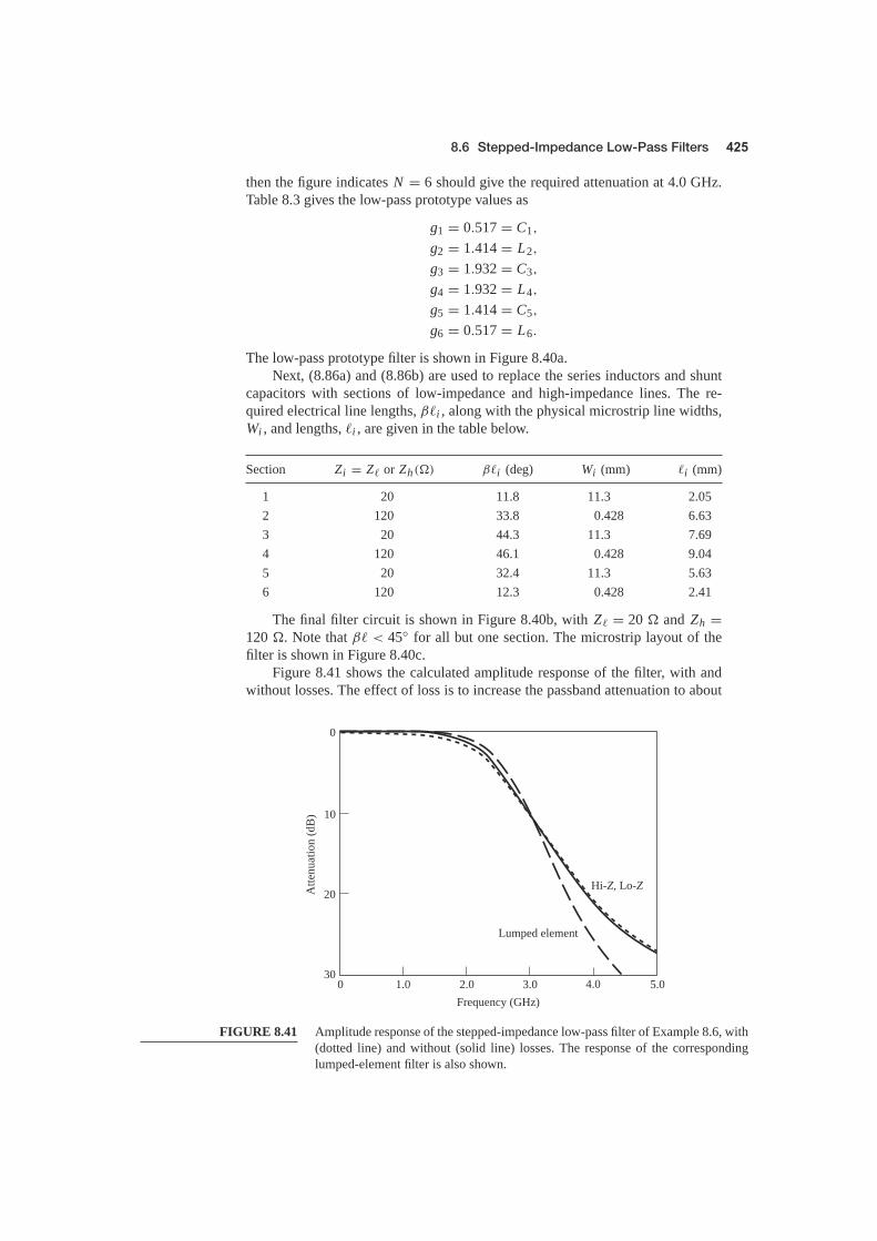
8.6 Stepped-Impedance Low-Pass Filters
then the figure indicates N = 6 should give the required attenuation at 4.0 GHz.Table 8.3 gives the low-pass prototype values as
g1 = 0.517 = C1,
g2 = 1.414 = L2,
g3 = 1.932 = C3,
g4 = 1.932 = L4,
g5 = 1.414 = C5,
g6 = 0.517 = L6.
The low-pass prototype filter is shown in Figure 8.40a.Next, (8.86a) and (8.86b) are used to replace the series inductors and shunt
capacitors with sections of low-impedance and high-impedance lines. The re-quired electrical line lengths, β�i , along with the physical microstrip line widths,Wi , and lengths, �i , are given in the table below.
Section Zi = Z� or Zh(�) β�i (deg) Wi (mm) �i (mm)
1 20 11.8 11.3 2.052 120 33.8 0.428 6.633 20 44.3 11.3 7.694 120 46.1 0.428 9.045 20 32.4 11.3 5.636 120 12.3 0.428 2.41
The final filter circuit is shown in Figure 8.40b, with Z� = 20 � and Zh =120 �. Note that β� < 45◦ for all but one section. The microstrip layout of thefilter is shown in Figure 8.40c.
Figure 8.41 shows the calculated amplitude response of the filter, with andwithout losses. The effect of loss is to increase the passband attenuation to about
0 1.0 2.0 3.0 5.030
10
0
Atte
nuat
ion
(dB
)
Frequency (GHz)
Lumped element
Hi-Z, Lo-Z20
4.0
FIGURE 8.41 Amplitude response of the stepped-impedance low-pass filter of Example 8.6, with(dotted line) and without (solid line) losses. The response of the correspondinglumped-element filter is also shown.
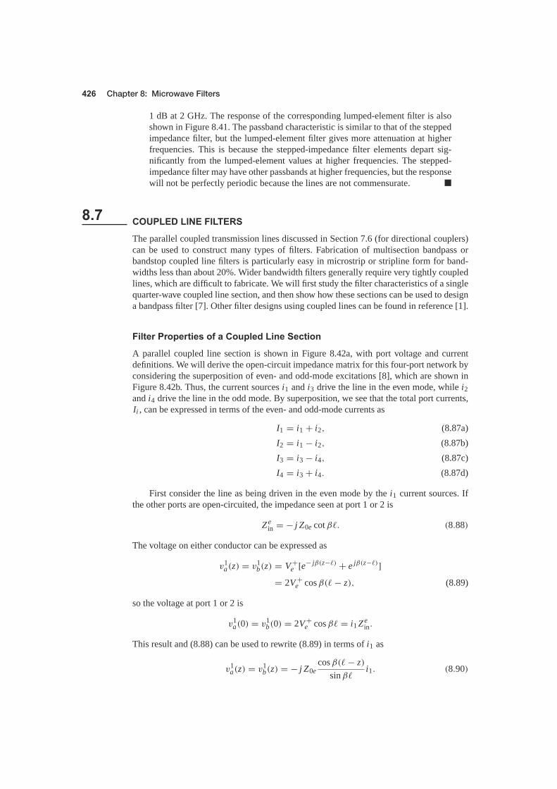
Chapter 8: Microwave Filters
1 dB at 2 GHz. The response of the corresponding lumped-element filter is alsoshown in Figure 8.41. The passband characteristic is similar to that of the steppedimpedance filter, but the lumped-element filter gives more attenuation at higherfrequencies. This is because the stepped-impedance filter elements depart sig-nificantly from the lumped-element values at higher frequencies. The stepped-impedance filter may have other passbands at higher frequencies, but the responsewill not be perfectly periodic because the lines are not commensurate. ■
The parallel coupled transmission lines discussed in Section 7.6 (for directional couplers)can be used to construct many types of filters. Fabrication of multisection bandpass orbandstop coupled line filters is particularly easy in microstrip or stripline form for band-widths less than about 20%. Wider bandwidth filters generally require very tightly coupledlines, which are difficult to fabricate. We will first study the filter characteristics of a singlequarter-wave coupled line section, and then show how these sections can be used to designa bandpass filter [7]. Other filter designs using coupled lines can be found in reference [1].
A parallel coupled line section is shown in Figure 8.42a, with port voltage and currentdefinitions. We will derive the open-circuit impedance matrix for this four-port network byconsidering the superposition of even- and odd-mode excitations [8], which are shown inFigure 8.42b. Thus, the current sources i1 and i3 drive the line in the even mode, while i2and i4 drive the line in the odd mode. By superposition, we see that the total port currents,Ii , can be expressed in terms of the even- and odd-mode currents as
I1 = i1 + i2, (8.87a)I2 = i1 − i2, (8.87b)I3 = i3 − i4, (8.87c)I4 = i3 + i4. (8.87d)
First consider the line as being driven in the even mode by the i1 current sources. Ifthe other ports are open-circuited, the impedance seen at port 1 or 2 is
Zein = − j Z0e cot β�. (8.88)
The voltage on either conductor can be expressed as
v1a(z) = v1
b(z) = V +e [e− jβ(z−�) + e jβ(z−�)]
= 2V +e cos β(� − z), (8.89)
so the voltage at port 1 or 2 is
v1a(0) = v1
b(0) = 2V +e cos β� = i1 Ze
in.
This result and (8.88) can be used to rewrite (8.89) in terms of i1 as
v1a(z) = v1
b(z) = − j Z0ecos β(� − z)
sin β�i1. (8.90)

8.7 Coupled Line Filters
1I1 4 I4
2I2 3 I3
+V2
+V1 +V4
+V3
Z0e, Z0o
0 lz
(a)
1i1 4 i3i4
2i1i2
3 i3Z0e, Z0o
vb
va
0 lz
(b)
1I1 4
2O.C. 3 I3Z0e, Z0o
(c)
O.C.
FIGURE 8.42 Definitions pertaining to a coupled line filter section. (a) A parallel coupled linesection with port voltage and current definitions. (b) A parallel coupled line sec-tion with even- and odd-mode current sources. (c) A two-port coupled line sectionhaving a bandpass response.
Similarly, the voltages due to current sources i3 driving the line in the even mode are
v3a(z) = v3
b(z) = − j Z0ecos βzsin β�
i3. (8.91)
Now consider the line as being driven in the odd mode by current i2. If the other portsare open-circuited, the impedance seen at port 1 or 2 is
Zoin = − j Z0o cot β�. (8.92)
The voltage on either conductor can be expressed as
v2a(z) = −v2
b(z) = V +0[e− jβ(z−�) + e jβ(z−�)
] = 2V +0 cos β(� − z). (8.93)
Then the voltage at port 1 or port 2 is
v2a(0) = −v2
b(0) = 2V +0 cos β� = i2 Zo
in.

Chapter 8: Microwave Filters
This result and (8.92) can be used to rewrite (8.93) in terms of i2 as
v2a(z) = −v2
b(z) = − j Z0ocos β(� − z)
sin β�i2. (8.94)
Similarly, the voltages due to current i4 driving the line in the odd mode are
v4a(z) = −v4
b(z) = − j Z0ocos βzsin β�
i4. (8.95)
The total voltage at port 1 is
V1 = v1a(0) + v2
a(0) + v3a(0) + v4
a(0)
= − j (Z0ei1 + Z0oi2) cot θ − j (Z0ei3 + Z0oi4) csc θ, (8.96)
where the results of (8.90), (8.91), (8.94), and (8.95) were used, and θ = β�. Next, wesolve (8.87) for the i j in terms of the I s:
i1 = 12(I1 + I2), (8.97a)
i2 = 12(I1 − I2), (8.97b)
i3 = 12(I3 + I4), (8.97c)
i4 = 12(I4 − I3), (8.97d)
and use these results in (8.96):
V1 = − j2
(Z0e I1 + Z0e I2 + Z0o I1 − Z0o I2) cot θ
− j2
(Z0e I3 + Z0e I4 + Z0o I4 − Z0o I3) csc θ. (8.98)
This result yields the top row of the open-circuit impedance matrix [Z ] that describes thecoupled line section. From symmetry, all other matrix elements can be found once the firstrow is known. The matrix elements are then
Z11 = Z22 = Z33 = Z44 = − j2
(Z0e + Z0o) cot θ (8.99a)
Z12 = Z21 = Z34 = Z43 = − j2
(Z0e − Z0o) cot θ (8.99b)
Z13 = Z31 = Z24 = Z42 = − j2
(Z0e − Z0o) csc θ (8.99c)
Z14 = Z41 = Z23 = Z32 = − j2
(Z0e + Z0o) csc θ (8.99d)
A two-port network can be formed from a coupled line section by terminating twoof the four ports with either open or short circuits, or by connecting two ends; there are10 possible combinations, as illustrated in Table 8.8. As indicated in the table, the variouscircuits have different frequency responses, including low-pass, bandpass, all pass, and allstop. For bandpass filters, we are most interested in the case shown in Figure 8.42c, as opencircuits are easier to fabricate in microstrip than are short circuits. In this case, I2 = I4 = 0,

8.7 Coupled Line Filters
TABLE 8.8 Ten Canonical Coupled Line Circuits
Circuit Image Impedance Response
Re(Zi1)
0Zi1 Zi2
Zi1
Zi1
Zi1
Zi2
Zi1
Zi1
Zi1
Zi1
Zi1 Zi1
Zi1
Zi2
Zi1
Zi1
Zi1 Zi1
Zi1
Zi1
232Low-pass
Re(Zi1)
02
32Bandpass
Re(Zi1)
02
32Bandpass
Re(Zi1)
02
32Bandpass
Zi1 =
Zi1Zi2 =
2Z0eZ0o cos
(Z0e + Z0o)2 cos 2 – (Z0e – Z0o)2
Z0eZ0o
Zi1 =2Z0eZ0o sin
(Z0e – Z0o)2 – (Z0e + Z0o)2 cos 2
Zi1 =2 sin
(Z0e – Z0o)2 – (Z0e + Z0o)2 cos 2
Zi1 =
Z0eZ0o
(Z0e – Z0o)2 – (Z0e + Z0o)2 cos 2
(Z0e + Z0o) sinZ0e Z0o
Zi1Zi2 =
Zi1 = –j
Z0eZ0o
Zi1Zi2 =
Z0eZ0o
2Zi1 =
Z0e + Z0o
Zi1 =
Zi1 =
Z0eZ0oZi1 = j
2Z0eZ0oZ0e + Z0o
2Z0eZ0oZ0e + Z0o
cot
tan
Z0eZ0oZi1 = –j cot
All pass
All pass
All pass
All stop
All stop
All stop

Chapter 8: Microwave Filters
00
�1 �2 �π �2 2
3�
Z0e – Z0o2
Re(Zi)
FIGURE 8.43 The real part of the image impedance of the bandpass network of Figure 8.42c.
so the four-port impedance matrix equations reduce to
V1 = Z11 I1 + Z13 I3, (8.100a)
V3 = Z31 I1 + Z33 I3, (8.100b)
where Zi j is given in (8.99).We can analyze the filter characteristics of this circuit by calculating the image imped-
ance (which is the same at ports 1 and 3), and the propagation constant. From Table 8.1,the image impedance in terms of the impedance parameters is
Zi =√
Z211 − Z11 Z2
13Z33
= 12
√(Z0e − Z0o)2 csc2 θ − (Z0e + Z0o)2 cot2 θ. (8.101)
When the coupled line section is λ/4 long (θ = π/2), the image impedance reduces to
Zi = 12(Z0e − Z0o), (8.102)
which is real and positive since Z0e > Z0o. However, when θ → 0 or π, Zi → ± j∞,indicating a stopband. The real part of the image impedance is sketched in Figure 8.43,where the cutoff frequencies can be found from (8.101) as
cos θ1 = − cos θ2 = Z0e − Z0o
Z0e + Z0o.
The propagation constant can also be calculated from the results of Table 8.1 as
cos β =√
Z11 Z33
Z213
= Z11
Z13= Z0e + Z0o
Z0e − Z0ocos θ, (8.103)
which shows β is real for θ1 < θ < θ2 = π − θ1, where cos θ1 = (Z0e − Z0o)/(Z0e +Z0o).
Narrowband bandpass filters can be made with cascaded coupled line sections of the formshown in Figure 8.42c. To derive the design equations for filters of this type, we first showthat a single coupled line section can be approximately modeled by the equivalent circuitshown in Figure 8.44. We will do this by calculating the image impedance and propagationconstant of the equivalent circuit and showing that they are approximately equal to those

8.7 Coupled Line Filters
��
J–90°Z0 Z0
FIGURE 8.44 Equivalent circuit of the coupled line section of Figure 8.42c.
of the coupled line section for θ = π/2, which will correspond to the center frequency ofthe bandpass response.
The ABCD parameters of the equivalent circuit can be computed using the ABCDmatrices for transmission lines from Table 4.1:
[A BC D
]=
⎡⎢⎣ cos θ j Z0 sin θ
j sin θ
Z0cos θ
⎤⎥⎦ [
0 − j/J− j J 0
]⎡⎢⎣ cos θ j Z0 sin θ
j sin θ
Z0cos θ
⎤⎥⎦
=
⎡⎢⎢⎢⎢⎢⎣
(J Z0 + 1
J Z0
)sin θ cos θ j
(J Z2
0 sin2 θ − cos2 θ
J
)
j
(1
J Z20
sin2 θ − J cos2 θ
) (J Z0 + 1
J Z0
)sin θ cos θ
⎤⎥⎥⎥⎥⎥⎦. (8.104)
The ABCD parameters of the admittance inverter were obtained by considering it as aquarter-wave length of transmission of characteristic impedance, 1/J . From (8.27) theimage impedance of the equivalent circuit is
Zi =√
BC
=√√√√ J Z2
0 sin2 θ − (1/J ) cos2 θ
(1/J Z20) sin2 θ − J cos2 θ
, (8.105)
which reduces to the following value at the center frequency, θ = π/2:
Zi = J Z20 . (8.106)
From (8.31) the propagation constant is
cos β = A =(
J Z0 + 1J Z0
)sin θ cos θ. (8.107)
Equating the image impedances in (8.102) and (8.106), and the propagation constants of(8.103) and (8.107), yields the following equations:
12(Z0e − Z0o) = J Z2
0,
Z0e + Z0o
Z0e − Z0o= J Z0 + 1
J Z0,
where we have assumed sin θ 1 for θ near π/2. These equations can be solved for theeven- and odd-mode line impedances to give
Z0e = Z0[1 + J Z0 + (J Z0)2], (8.108a)
Z0o = Z0[1 − J Z0 + (J Z0)2]. (8.108b)
Now consider a bandpass filter composed of a cascade of N + 1 coupled line sections,as shown in Figure 8.45a. The sections are numbered from left to right, with the load on the

Chapter 8: Microwave Filters
FIGURE 8.45 Development of an equivalent circuit for derivation of design equations for a cou-pled line bandpass filter. (a) Layout of an (N + 1)-section coupled line bandpassfilter. (b) Using the equivalent circuit of Figure 8.44 for each coupled line section.(c) Equivalent circuit for transmission lines of length 2θ . (d) Equivalent circuitof the admittance inverters. (e) Using results of (c) and (d) for the N = 2 case.(f) Lumped-element circuit for a bandpass filter for N = 2.

8.7 Coupled Line Filters
right, but the filter can be reversed without affecting the response. Since each coupled linesection has an equivalent circuit of the form shown in Figure 8.44, the equivalent circuit ofthe cascade is as shown in Figure 8.45b. Between any two consecutive inverters we havea transmission line section that is effectively 2θ in length. This line is approximately λ/2long in the vicinity of the bandpass region of the filter, and has an approximate equivalentcircuit that consists of a shunt parallel LC resonator, as in Figure 8.45c.
The first step in establishing this equivalence is to find the parameters for the T-equivalent and ideal transformer circuit of Figure 8.45c (an exact equivalent). The ABCDmatrix for this circuit can be calculated using the results in Table 4.1 for a T-circuit and anideal transformer:
[A BC D
]=
⎡⎢⎢⎣
Z11
Z12
Z211 − Z2
12Z12
1Z12
Z11
Z12
⎤⎥⎥⎦[−1 0
0 −1
]=
⎡⎢⎢⎣
−Z11
Z12
Z212 − Z2
11Z12
−1Z12
−Z11
Z12
⎤⎥⎥⎦. (8.109)
Equating this result to the ABCD parameters for a transmission line of length 2θ and char-acteristic impedance Z0 gives the parameters of the equivalent circuit as
Z12 = −1C
= j Z0
sin 2θ, (8.110a)
Z11 = Z22 = −Z12 A = − j Z0 cot 2θ. (8.110b)
Then the series arm impedance is
Z11 − Z12 = − j Z0cos 2θ + 1
sin 2θ= − j Z0 cot θ. (8.111)
The 1: −1 transformer provides a 180◦ phase shift, which cannot be obtained with theT-network alone; since this does not affect the amplitude response of the filter, it can bediscarded. For θ ∼ π/2 the series arm impedances of (8.111) are near zero and can also beignored. The shunt impedance Z12, however, looks like the impedance of a parallel reso-nant circuit for θ ∼ π/2. If we let ω = ω0 + �ω, where θ = π/2 at the center frequencyω0, then we have 2θ = β� = ω�/vp = (ω0 + �ω)π/ω0 = π(1 + �ω/ω0), so (8.110a)can be written for small �ω as
Z12 = j Z0
sin π(1 + �ω/ω0) − j Z0ω0
π(ω − ω0). (8.112)
From Section 6.1 the impedance near resonance of a parallel LC circuit is
Z = − j Lω20
2(ω − ω0), (8.113)
with ω20 = 1/LC . Equating this to (8.112) gives the equivalent inductor and capacitor val-
ues as
L = 2Z0
πω0, (8.114a)
C = 1ω2
0 L= π
2Z0ω0. (8.114b)
The end sections of the circuit of Figure 8.45b require a different treatment. The linesof length θ on either end of the filter are matched to Z0 and so can be ignored. The endinverters, J1 and JN+1, can each be represented as a transformer followed by a λ/4 section

Chapter 8: Microwave Filters
of line, as shown in Figure 8.45d. The ABCD matrix of a transformer with a turns ratio Nin cascade with a quarter-wave line is
[A BC D
]=
[ 1N
0
0 N
] [ 0 − j Z0− jZ0
0
]=
⎡⎣ 0
− j Z0
N− j NZ0
0
⎤⎦. (8.115)
Comparing this to the ABCD matrix of an admittance inverter [part of (8.104)] shows thatthe necessary turns ratio is N = J Z0. The λ/4 line merely produces a phase shift and socan be ignored.
Using these results for the interior and end sections allows the circuit of Figure 8.45bto be transformed into the circuit of Figure 8.45e, which is specialized to the N = 2 case.We see that each pair of coupled line sections leads to an equivalent shunt LC resonator,and an admittance inverter occurs between each pair of LC resonators. Next, we showthat the admittance inverters have the effect of transforming a shunt LC resonator intoa series LC resonator, leading to the final equivalent circuit of Figure 8.45f (shown forN = 2). This will then allow the admittance inverter constants, Jn , to be determined fromthe element values of a low-pass prototype. We will demonstrate this for the N = 2 case.
With reference to Figure 8.45e, the admittance just to the right of the J2 inverter is
jωC2 + 1jωL2
+ Z0 J 23 = j
√C2
L2
(ω
ω0− ω0
ω
)+ Z0 J 2
3 ,
since the transformer scales the load admittance by the square of the turns ratio. Then theadmittance seen at the input of the filter is
Y = 1J 2
1 Z20
{jωC1 + 1
jωL1+ J 2
2j√
C2/L2 [(ω/ω0) − (ω0/ω)] + Z0 J 23
}
= 1J 2
1 Z20
{j
√C1
L1
(ω
ω0− ω0
ω
)+ J 2
2j√
C2/L2 [(ω/ω0) − (ω0/ω)] + Z0 J 23
}. (8.116)
These results also use the fact, from (8.114), that LnCn = 1/ω20 for all LC resonators.
Now the admittance seen looking into the circuit of Figure 8.45f is
Y = jωC ′1 + 1
jωL ′1
+ 1jωL ′
2 + 1/jωC ′2 + Z0
= j
√C ′
1L ′
1
(ω
ω0− ω0
ω
)+ 1
j√
L ′2/C ′
2 [(ω/ω0) − (ω0/ω)] + Z0
, (8.117)
which is identical in form to (8.116). Thus, the two circuits will be equivalent if the fol-lowing conditions are met:
1J 2
1 Z20
√C1
L1=
√C ′
1L ′
1, (8.118a)
J 21 Z2
0J 2
2
√C2
L2=
√L ′
2C ′
2, (8.118b)
J 21 Z3
0 J 23
J 22
= Z0. (8.118c)

8.7 Coupled Line Filters
We know Ln and Cn from (8.114); L ′n and C ′
n are determined from the element valuesof a lumped-element low-pass prototype that has been impedance scaled and frequencytransformed to a bandpass filter. Using the results in Table 8.6 and the impedance scalingformulas of (8.64) allows the L ′
n and C ′n values to be written as
L ′1 = �Z0
ω0g1, (8.119a)
C ′1 = g1
�ω0 Z0, (8.119b)
L ′2 = g2 Z0
�ω0, (8.119c)
C ′2 = �
ω0g2 Z0, (8.119d)
where � = (ω2 − ω1)/ω0 is the fractional bandwidth of the filter. Then (8.118) can besolved for the inverter constants with the following results (for N = 2):
J1 Z0 =(C1L ′
1L1C ′
1
)1/4=
√π�
2g1, (8.120a)
J2 Z0 = J1 Z20
(C2C ′2
L2L ′2
)1/4= π�
2√g1g2, (8.120b)
J3 Z0 = J2
J1=
√π�
2g2. (8.120c)
After the Jn are found, Z0e and Z0o for each coupled line section can be calculated from(8.108).
The above results were derived for the special case of N = 2 (three coupled line sec-tions), but more general results can be derived for any number of sections, and for the casewhere ZL �= Z0 (or gN+1 �= 1, as in the case of an equal-ripple response with N even).Thus, the design equations for a bandpass filter with N + 1 coupled line sections are
Z0 J1 =√
π�
2g1, (8.121a)
Z0 Jn = π�
2√gn−1gnfor n = 2, 3, . . . , N , (8.121b)
Z0 JN+1 =√
π�
2gN gN+1. (8.121c)
The even- and odd-mode characteristic impedances for each section are found from (8.108).
EXAMPLE 8.7 COUPLED LINE BANDPASS FILTER DESIGN
Design a coupled line bandpass filter with N = 3 and a 0.5 dB equal-ripple re-sponse. The center frequency is 2.0 GHz, the bandwidth is 10%, and Z0 = 50 �.What is the attenuation at 1.8 GHz?
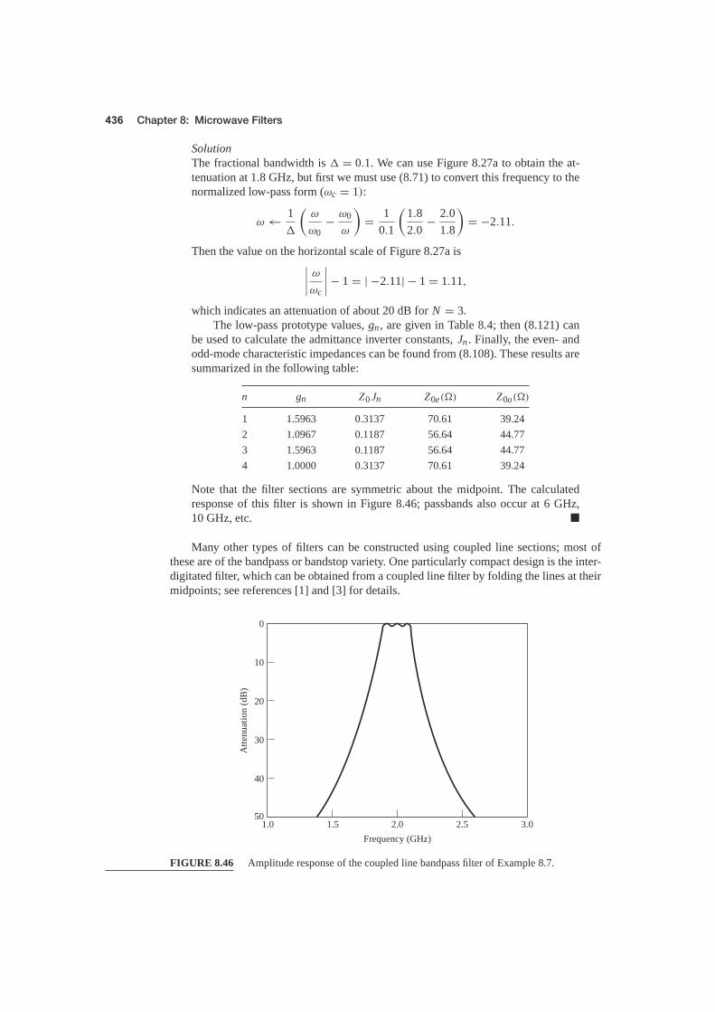
Chapter 8: Microwave Filters
SolutionThe fractional bandwidth is � = 0.1. We can use Figure 8.27a to obtain the at-tenuation at 1.8 GHz, but first we must use (8.71) to convert this frequency to thenormalized low-pass form (ωc = 1):
ω ← 1�
(ω
ω0− ω0
ω
)= 1
0.1
(1.82.0
− 2.01.8
)= −2.11.
Then the value on the horizontal scale of Figure 8.27a is∣∣∣∣ ω
ωc
∣∣∣∣ − 1 = | −2.11| − 1 = 1.11,
which indicates an attenuation of about 20 dB for N = 3.The low-pass prototype values, gn , are given in Table 8.4; then (8.121) can
be used to calculate the admittance inverter constants, Jn . Finally, the even- andodd-mode characteristic impedances can be found from (8.108). These results aresummarized in the following table:
n gn Z0 Jn Z0e(�) Z0o(�)
1 1.5963 0.3137 70.61 39.242 1.0967 0.1187 56.64 44.773 1.5963 0.1187 56.64 44.774 1.0000 0.3137 70.61 39.24
Note that the filter sections are symmetric about the midpoint. The calculatedresponse of this filter is shown in Figure 8.46; passbands also occur at 6 GHz,10 GHz, etc. ■
Many other types of filters can be constructed using coupled line sections; most ofthese are of the bandpass or bandstop variety. One particularly compact design is the inter-digitated filter, which can be obtained from a coupled line filter by folding the lines at theirmidpoints; see references [1] and [3] for details.
1.0 1.5 2.0 2.5 3.050
40
30
20
10
0
Atte
nuat
ion
(dB
)
Frequency (GHz)
FIGURE 8.46 Amplitude response of the coupled line bandpass filter of Example 8.7.

8.8 Filters Using Coupled Resonators
We have seen that bandpass and bandstop filters require elements that behave as series orparallel resonant circuits; the coupled line bandpass filters of the previous section were ofthis type. Here we will consider several other types of microwave filters that use transmis-sion line or cavity resonators.
From Chapter 6 we know that quarter-wave open-circuited or short-circuited transmissionline stubs look like series or parallel resonant circuits, respectively. We can therefore usesuch stubs in shunt along a transmission line to implement bandpass or bandstop filters,as shown in Figure 8.47. Quarter-wavelength sections of line between the stubs act asadmittance inverters to effectively convert alternate shunt resonators to series resonators.The stubs and the transmission line sections are λ/4 long at the center frequency, ω0.
For narrow bandwidths the response of such a filter using N stubs is essentially thesame as that of a coupled line filter using N + 1 sections. The internal impedance of thestub filter is Z0, while in the case of the coupled line filter end sections are required to trans-form the impedance level. This makes the stub filter more compact and easier to design.A disadvantage, however, is that a filter using stub resonators often requires characteristicimpedances that are difficult to realize in practice.
We first consider a bandstop filter using N open-circuited stubs, as shown in Fig-ure 8.47a. The design equations for the required stub characteristic impedances, Z0n , willbe derived in terms of the element values of a low-pass prototype through the use of anequivalent circuit. The analysis of the bandpass version, using short-circuited stubs, fol-lows the same procedure, so the design equations for this case are presented without de-tailed derivation.
As indicated in Figure 8.48a, an open-circuited stub can be approximated as a se-ries LC resonator when its length is near 90◦. The input impedance of an open-circuited
�
� �
Z0Z0
Z0N
Z0N – 1
�
� �
Z0 Z0
Z02 Z01
(a)
�
� �
Z0Z0
Z0N
Z0N – 1
�
� �
Z0 Z0
Z02 Z01
(b)
FIGURE 8.47 Bandstop and bandpass filters using shunt transmission line resonators (θ = π/2at the center frequency). (a) Bandstop filter. (b) Bandpass filter.

Chapter 8: Microwave Filters
CN
J = 1/Z0–90°
J = 1/Z0–90°
J = 1/Z0–90° Z0
Z0
LN
Cn
Ln
L3
C3
L2
C2
L1
C1
L3' L1'
C3' C1'
C2'
L2'
Y
Y
(c)
(b)
(a)� = �/2 at = 0
Z
Z0n
�
FIGURE 8.48 Equivalent circuit for the bandstop filter of Figure 8.47a. (a) Equivalent circuit ofan open-circuited stub for θ near π/2. (b) Equivalent filter circuit using resonatorsand admittance inverters. (c) Equivalent lumped-element bandstop filter.
transmission line of characteristic impedance Z0n is
Z = − j Z0n cot θ,
where θ = π/2 for ω = ω0. If we let ω = ω0 + �ω, where �ω ω0, then θ = (π/2)
(1 + �ω/ω0), and this impedance can be approximated as
Z = j Z0n tanπ�ω
2ω0 j Z0nπ(ω − ω0)
2ω0(8.122)
for frequencies in the vicinity of the center frequency, ω0. The impedance of a series LCcircuit is
Z = jωLn + 1jωCn
= j
√Ln
Cn
(ω
ω0− ω0
ω
) 2 j
√Ln
Cn
ω − ω0
ω0 2 j Ln(ω − ω0),
(8.123)
where LnCn = 1/ω20. Equating (8.122) and (8.123) gives the characteristic impedance of
the stub in terms of the resonator parameters:
Z0n = 4ω0Ln
π. (8.124)

8.8 Filters Using Coupled Resonators
Then, if we consider the quarter-wave sections of line between the stubs as ideal ad-mittance inverters, the bandstop filter of Figure 8.47a can be represented by the equivalentcircuit of Figure 8.48b. Next, the circuit elements of this equivalent circuit can be relatedto those of the lumped-element bandstop filter prototype of Figure 8.48c.
With reference to Figure 8.48b, the admittance Y seen looking toward the L2C2 res-onator is
Y = 1jωL2 + (1/jωC2)
+ 1Z2
0
(1
jωL1 + 1/jωC1+ 1
Z0
)−1
= 1j√
L2/C2[(ω/ω0) − (ω0/ω)
]+ 1
Z0
{1
j√
L1/C1[(ω/ω0) − (ω0/ω)
] + 1Z0
}. (8.125)
The admittance at the corresponding point in the circuit of Figure 8.48c is
Y = 1jωL ′
2 + 1/jωC ′2
+(
1jωC ′
1 + 1/jωL ′1
+ Z0
)−1
= 1
j√
L ′2/C ′
2[(ω/ω0) − (ω0/ω)
]+
⎧⎨⎩ 1
j√
C ′1/L ′
1[(ω/ω0) − (ω0/ω)
] + Z0
⎫⎬⎭
−1
. (8.126)
These two results will be equivalent if the following conditions are satisfied:
1Z2
0
√L1
C1=
√C ′
1L ′
1, (8.127a)√
L2
C2=
√L ′
2C ′
2. (8.127b)
Since LnCn = L ′nC ′
n = 1/ω20, these results can be solved for Ln :
L1 = Z20
ω20 L ′
1, (8.128a)
L2 = L ′2. (8.128b)
Using (8.124) and the impedance-scaled bandstop filter elements from Table 8.6 gives thestub characteristic impedances as
Z01 = 4Z20
πω0L ′1
= 4Z0
πg1�, (8.129a)
Z02 = 4ω0L ′2
π= 4Z0
πg2�, (8.129b)
where � = (ω2 − ω1)/ω0 is the fractional bandwidth of the filter. It is easy to show thatthe general result for the characteristic impedances of a bandstop filter is
Z0n = 4Z0
πgn�. (8.130)

Chapter 8: Microwave Filters
For a bandpass filter using short-circuited stub resonators the corresponding result is
Z0n = π Z0�
4gn. (8.131)
These results only apply to filters having input and output impedances of Z0 and so cannotbe used for equal-ripple designs with N even.
EXAMPLE 8.8 BANDSTOP FILTER DESIGN
Design a bandstop filter using three quarter-wave open-circuit stubs. The centerfrequency is 2.0 GHz, the bandwidth is 15%, and the impedance is 50 �. Use anequal-ripple response, with a 0.5 dB ripple level.
SolutionThe fractional bandwidth is � = 0.15. Table 8.4 gives the low-pass prototypevalues, gn , for N = 3. Then the characteristic impedances of the stubs can befound from (8.130). The results are listed in the following table:
n gn Z0n(�)
1 1.5963 265.92 1.0967 387.03 1.5963 265.9
The filter circuit is shown in Figure 8.47a, with all stubs and transmission linesections λ/4 long at 2.0 GHz. The calculated attenuation for this filter is shown inFigure 8.49; the ripple in the passbands is somewhat greater than 0.5 dB as a resultof the approximations involved in the development of the design equations. ■
The performance of quarter-wave resonator filters can be improved by allowing thecharacteristic impedances of the interconnecting lines to be variable; then an exact cor-respondence with coupled line bandpass or bandstop filters can be demonstrated. Designdetails for this case can be found in reference [1].
1.0 1.5 2.0 2.5 3.050
40
30
20
10
0
Atte
nuat
ion
(dB
)
Frequency (GHz)
FIGURE 8.49 Amplitude response of the bandstop filter of Example 8.8.

8.8 Filters Using Coupled Resonators
J1+90°
J2+90°
JN + 1+90°
Z0
Z0
Z0 Z0
Z0 Z0
Z0 Z0
Z0
Z0 Z0 Z0Z0
Z0
B1
�1
�1
�1
�2 �3
�2
�N
�N
B2 B3 BN + 1
jB1
jB1
jB2
jB2
jB3 jBN jBN + 1
jBN + 12�12
�22
�2�
Z0Z0Z0
Z0 Z0 Z0 Z0
Z0 Z0
�
� �
2
�N + 12
�N + 12
(d)
(c)
(b)
(a)
FIGURE 8.50 Development of the equivalence of a capacitive-gap coupled resonator bandpassfilter to the coupled line bandpass filter of Figure 8.45. (a) The capacitive-gapcoupled resonator bandpass filter. (b) Transmission line model. (c) Transmissionline model with negative-length sections forming admittance inverters (φi /2 < 0).(d) Equivalent circuit using inverters and λ/2 resonators (φ = π at ω0). This cir-cuit is identical in form with the coupled line bandpass filter equivalent circuit ofFigure 8.45b.
Another type of bandpass filter that can be conveniently fabricated in microstrip or striplineform is the capacitive-gap coupled resonator filter shown in Figure 8.50. An N th-orderfilter of this form will use N resonant series sections of transmission line with N + 1capacitive gaps between them. These gaps can be approximated as series capacitors; designdata relating the capacitance to the gap size and transmission line parameters is given ingraphical form in reference [1]. The filter can then be modeled as shown in Figure 8.50b.The resonators are approximately λ/2 long at the center frequency, ω0.
Next, we redraw the equivalent circuit of Figure 8.50b with negative-length transmis-sion line sections on either side of the series capacitors. The lines of length φ will be λ/2long at ω0, so the electrical length θi of the i th section in Figures 8.50a, b is
θi = π + 12φi + 1
2φi+1 for i = 1, 2, . . . , N , (8.132)
with φi < 0. The reason for doing this is that the combination of series capacitor andnegative-length transmission lines forms the equivalent circuit of an admittance inverter, asseen from Figure 8.38c. In order for this equivalence to be valid, the following relationship

Chapter 8: Microwave Filters
must hold between the electrical length of the lines and the capacitive susceptance:
φi = − tan−1(2Z0 Bi ). (8.133)
Then the resulting inverter constant can be related to the capacitive susceptance as
Bi = Ji
1 − (Z0 Ji )2 . (8.134)
(These results are given in Figure 8.38, and their derivation is requested in Problem 8.14.)The capacitive-gap coupled filter can then be modeled as shown in Figure 8.50d. Now
consider the equivalent circuit shown in Figure 8.45b for a coupled line bandpass filter.Since these two circuits are identical (as φ = 2θ = π at the center frequency), we can usethe results from the coupled line filter analysis to complete the present problem. Thus,we can use (8.121) to find the admittance inverter constants, Ji , from the low-pass proto-type values, gi , and the fractional bandwidth, �. As in the case of the coupled line filter,there will be N + 1 inverter constants for an N th-order filter. Then (8.134) can be usedto find the susceptance, Bi , for the i th coupling gap. Finally, the electrical length of theresonator sections can be found from (8.132) and (8.133):
θi = π − 12[tan−1(2Z0 Bi ) + tan−1(2Z0 Bi+1)]. (8.135)
EXAMPLE 8.9 CAPACITIVELY COUPLED SERIES RESONATOR BANDPASSFILTER DESIGN
Design a bandpass filter using capacitive coupled series resonators, with a 0.5 dBequal-ripple passband characteristic. The center frequency is 2.0 GHz, the band-width is 10%, and the impedance is 50 �. At least 20 dB of attenuation is requiredat 2.2 GHz.
SolutionWe first determine the order of the filter to satisfy the attenuation specification at2.2 GHz. Using (8.71) to convert to normalized frequency gives
ω ← 1�
(ω
ω0− ω0
ω
)= 1
0.1
(2.22.0
− 2.02.2
)= 1.91.
Then, ∣∣∣∣ ω
ωc
∣∣∣∣ − 1 = 1.91 − 1.0 = 0.91.
From Figure 8.27a, we see that N = 3 should satisfy the attenuation specificationat 2.2 GHz. The low-pass prototype values are given in Table 8.4, from which theinverter constants can be calculated using (8.121). Then the coupling susceptancescan be found from (8.134), and the coupling capacitor values as
Cn = Bn
ω0.
Finally, the resonator lengths can be calculated from (8.135). The following tablesummarizes these results.
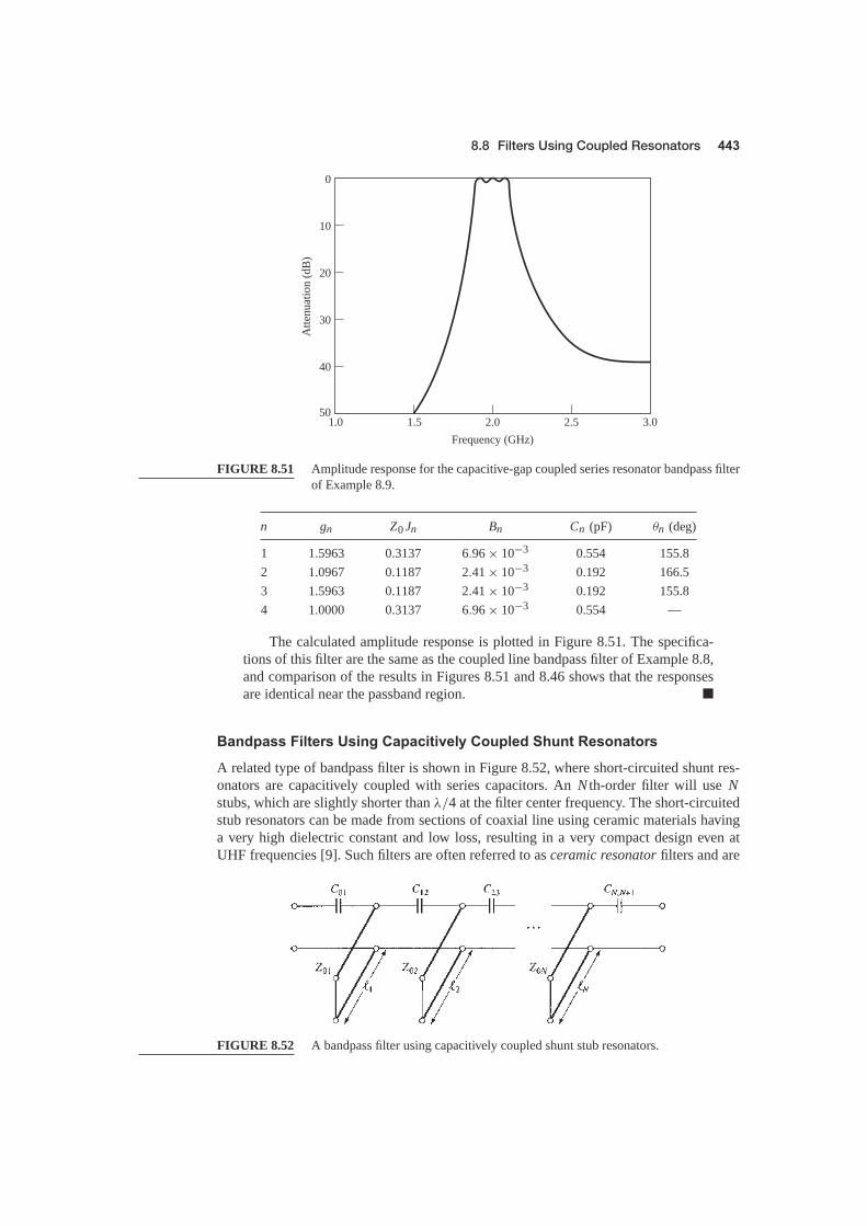
8.8 Filters Using Coupled Resonators
1.0 1.5 2.0 2.5 3.050
40
30
20
10
0
Atte
nuat
ion
(dB
)
Frequency (GHz)
FIGURE 8.51 Amplitude response for the capacitive-gap coupled series resonator bandpass filterof Example 8.9.
n gn Z0 Jn Bn Cn (pF) θn (deg)
1 1.5963 0.3137 6.96 × 10⁻³ 0.554 155.82 1.0967 0.1187 2.41 × 10⁻³ 0.192 166.53 1.5963 0.1187 2.41 × 10⁻³ 0.192 155.84 1.0000 0.3137 6.96 × 10⁻³ 0.554 —
The calculated amplitude response is plotted in Figure 8.51. The specifica-tions of this filter are the same as the coupled line bandpass filter of Example 8.8,and comparison of the results in Figures 8.51 and 8.46 shows that the responsesare identical near the passband region. ■
A related type of bandpass filter is shown in Figure 8.52, where short-circuited shunt res-onators are capacitively coupled with series capacitors. An N th-order filter will use Nstubs, which are slightly shorter than λ/4 at the filter center frequency. The short-circuitedstub resonators can be made from sections of coaxial line using ceramic materials havinga very high dielectric constant and low loss, resulting in a very compact design even atUHF frequencies [9]. Such filters are often referred to as ceramic resonator filters and are
FIGURE 8.52 A bandpass filter using capacitively coupled shunt stub resonators.

Chapter 8: Microwave Filters
among the most common types of RF bandpass filters used in portable wireless systems.Most cellular telephones, GPS receivers, and other wireless devices employ two or morefilters of this type.
Operation and design of this filter can be understood by beginning with the generalbandpass filter circuit of Figure 8.53a, where shunt LC resonators alternate with admit-tance inverters. As in the case of previous coupled resonator bandpass and bandstop filters,the function of the admittance inverters is to convert alternate shunt resonators to seriesresonators; the extra inverters at the ends serve to scale the impedance level of the filter toa realistic level. Using an analysis similar to that used for the bandstop filter, we can derivethe admittance inverter constants as
Z0 J01 =√
π�
4g1, (8.136a)
Z0 Jn, n+1 = π�
4√gngn+1, (8.136b)
Z0 JN , N+1 =√
π�
4gN gN+1. (8.136c)
Similarly, the coupling capacitor values can be found as
C01 = J01
ω0√
1 − (Z0 J01)2, (8.137a)
Cn, n+1 = Jn, n+1
ω0, (8.137b)
CN , N+1 = JN , N+1
ω0√
1 − (Z0 JN , N+1)2. (8.137c)
Note that the end capacitors are treated differently than the internal elements.Next, we replace the admittance inverters of Figure 8.53a with the equivalent π-
network of Figure 8.38d, to produce the equivalent lumped-element circuit shown in Figure8.53b. Note that the shunt capacitors of the admittance inverter circuits are negative, butthese elements combine in parallel with the larger capacitor of the LC resonator to yield anet capacitance value that is positive. The resulting circuit is shown in Figure 8.53c, wherethe effective resonator capacitor values are given by
C ′n = Cn + �Cn = Cn − Cn−1, n − Cn, n+1, (8.138)
where �Cn = −Cn−1,n − Cn,n+1 represents the change in the resonator capacitancecaused by the parallel addition of the inverter elements.
Finally, the shunt LC resonators of Figure 8.53c are replaced with short-circuited trans-mission stubs, as in the circuit of Figure 8.52. Note that the resonant frequency of the stubresonators is no longer ω0, since the resonator capacitor values have been modified by the�Cn . This implies that the length of the resonator is less than λ/4 at ω0, the filter centerfrequency. The transformation of the stub length to account for the change in capacitanceis illustrated in Figure 8.53d. A short-circuited length of line with a shunt capacitor at its

8.8 Filters Using Coupled Resonators
FIG
UR
E8.
53Eq
uiva
lent
circ
uitf
orth
eba
ndpa
ssfil
ter
ofFi
gure
8.52
.(a)
Age
nera
lban
dpas
sfil
ter
circ
uitu
sing
shun
tres
onat
ors
with
adm
ittan
cein
verte
rs.(
b)R
epla
cem
ento
fadm
ittan
cein
verte
rsw
ithth
eci
rcui
tim
plem
enta
tion
ofFi
gure
8.38
d.(c
)Afte
rcom
bini
ngsh
untc
apac
itor
elem
ents
.(d)
Cha
nge
inre
sona
ntst
uble
ngth
caus
edby
ash
untc
apac
itor.

Chapter 8: Microwave Filters
input has an input admittance of
Y = YL + jω0C, (8.139a)
where
YL = − j cot β�
Z0.
If the capacitor is replaced with a short length, ��, of transmission line, the input admit-tance would be
Y = 1Z0
YL + j 1Z0
tan �
1Z0
+ jYL tan �
∼= YL + jβ��
Z0. (8.139b)
The last approximation follows for � 1, which is true in practice for filters of thistype. Comparing (8.139b) with (8.139a) gives the change in stub length in terms of thecapacitor value:
�� = Z0ω0Cβ
=(
Z0ω0C2π
)λ. (8.140)
Note that if C < 0, then �� < 0, indicating a shortening of the stub length. Thus the overallstub length is given by
�n = λ
4+
(Z0ω0�Cn
2π
)λ, (8.141)
where �Cn is defined in (8.138). The characteristic impedance of the stub resonators is Z0.Dielectric material properties play a critical role in the performance of ceramic res-
onator filters. Materials with high dielectric constants are required in order to provideminiaturization at the frequencies typically used for wireless applications. Losses mustbe low to provide resonators with high Q, leading to low passband insertion loss andmaximum attenuation in the stopbands. In addition, the dielectric constant must be stablewith changes in temperature to avoid drifting of the filter passband over normal operat-ing conditions. Most materials that are commonly used in dielectric resonator filters areceramics, such as barium tetratitanate, zinc/strontium titanate, and various titanium oxidecompounds. For example, a zinc/strontium titanate ceramic material has a dielectric con-stant of 36, a Q of 10,000 at 4 GHz, and a dielectric constant temperature coefficient of−7 ppm/C◦.
EXAMPLE 8.10 CAPACITIVELY COUPLED SHUNT RESONATOR BANDPASSFILTER DESIGN
Design a third-order bandpass filter with a 0.5 dB equal-ripple response usingcapacitively coupled short-circuited shunt stub resonators. The center frequency is2.5 GHz, and the bandwidth is 10%. The impedance is 50 �. What is the resultingattenuation at 3.0 GHz?
SolutionWe first calculate the attenuation at 3.0 GHz. Using (8.71) to convert 3.0 GHz tonormalized low-pass form gives
ω ← 1�
(ω
ω0− ω0
ω
)= 1
0.1
(3.02.5
− 2.53.0
)= 3.667.

8.8 Filters Using Coupled Resonators
Then, to use Figure 8.27a, the value on the horizontal axis is∣∣∣∣ ω
ωc
∣∣∣∣ − 1 = |−3.667| − 1 = 2.667,
from which we find the attenuation as 35 dB.Next we calculate the admittance inverter constants and coupling capacitor
values using (8.136) and (8.137):
n gn Z0 Jn−1, n Cn−1, n (pF)
1 1.5963 Z0 J01 = 0.2218 C01 = 0.28962 1.0967 Z0 J12 = 0.0594 C12 = 0.07563 1.5963 Z0 J23 = 0.0594 C23 = 0.07564 1.0000 Z0 J34 = 0.2218 C34 = 0.2896
Then we use (8.138), (8.140), and (8.141) to find the required resonator lengths:
n �Cn (pF) ��n(λ) � (deg)
1 −0.3652 −0.04565 73.62 −0.1512 −0.0189 83.23 −0.3652 −0.04565 73.6
Note that the resonator lengths are slightly less than 90◦ (λ/4). The calculatedamplitude response of this design is shown in Figure 8.54. The stopband rolloff athigh frequencies is less than at lower frequencies, and the attenuation at 3 GHz isseen to be about 30 dB, while our calculated value for a canonical lumped-elementbandpass filter was 35 dB. ■
FIGURE 8.54 Amplitude response of the capacitively coupled shunt resonator bandpass filter ofExample 8.10.

Chapter 8: Microwave Filters
FIGURE 8.55 Photograph of a wideband down converter. Multiple PIN diode switches, filterbanks, amplifiers, and mixers are used to cover the range of 10 MHz to 27 GHz.Several types of filters can be seen in this module, including stub filters, coupledline filters, and stepped impedance filters. The microstrip stub filter at left is a low-pass 21-pole filter with a cutoff frequency of 5.4 GHz and more than 75 dB ofrejection from 5.8 to 9.0 GHz.Courtesy of LNX Corporation, Salem, N.H.
Figure 8.55 shows a wideband receiver downconverter module employing a variety ofdifferent filter types.
[1] G. L. Matthaei, L. Young, and E. M. T. Jones, Microwave Filters, Impedance-Matching Networks,and Coupling Structures, Artech House, Dedham, Mass., 1980.
[2] R. E. Collin, Foundations for Microwave Engineering, 2nd edition, Wiley-IEEE Press, Hoboken,N.J., 2001.
[3] J. A. G. Malherbe, Microwave Transmission Line Filters, Artech House, Dedham, Mass., 1979.[4] W. A. Davis, Microwave Semiconductor Circuit Design, Van Nostrand Reinhold, New York, 1984.[5] R. F. Harrington, Time-Harmonic Electromagnetic Fields, McGraw-Hill, New York, 1961.[6] P. I. Richards, “Resistor-Transmission Line Circuits,” Proceedings of the IRE, vol. 36, pp. 217–220,
February 1948.[7] S. B. Cohn, “Parallel-Coupled Transmission-Line-Resonator Filters,” IRE Transactions on Micro-
wave Theory and Techniques, vol. MTT-6, pp. 223–231, April 1958.[8] E. M. T. Jones and J. T. Bolljahn, “Coupled-Strip-Transmission Line Filters and Directional Cou-
plers,” IRE Transactions on Microwave Theory and Techniques, vol. MTT-4, pp. 78–81, April 1956.[9] M. Sagawa, M. Makimoto, and S. Yamashita, “A Design Method of Bandpass Filters Using
Dielectric-Filled Coaxial Resonators,” IEEE Transactions on Microwave Theory and Techniques,vol. MTT-33, pp. 152–157, February 1985.
8.1 Sketch the k-β diagram for the infinite periodic structure shown below. Assume Z0 = 75 �, d =1.0 cm, k = k0, and L0 = 1.25 nH.

Problems
d
L0
Z0, k
L0 L0 L0
8.2 Verify the expression for the image impedance of a π -network given in Table 8.1.8.3 Compute the image impedances and propagation factor for the network shown below.
L
L
C
Port1
Port2
8.4 Design a composite low-pass filter by the image parameter method with the following specifications:R0 = 50 �, fc = 50 MHz, and f∞ = 52 MHz. Use CAD to plot the insertion loss versus frequency.
8.5 Design a composite high-pass filter by the image parameter method with the following specifications:R0 = 75 �, fc = 50 MHz, and f∞ = 48 MHz. Use CAD to plot the insertion loss versus frequency.
8.6 Solve the design equations in Section 8.3 for the elements of an N = 2 equal-ripple filter if the ripplespecification is 1.0 dB.
8.7 Design a low-pass, maximally flat lumped-element filter having a passband of 0–2 GHz, and anattenuation of at least 20 dB at 3.4 GHz. The characteristic impedance is 50 �. Use CAD to plot theinsertion loss versus frequency.
8.8 Design a high-pass lumped-element filter with a 3 dB equal-ripple response, a cutoff frequency of3 GHz, and at least 30 dB insertion loss at 2.0 GHz. The characteristic impedance is 75 �. Use CADto plot the insertion loss versus frequency.
8.9 Design a four-section bandpass lumped-element filter having a maximally flat group delay response.The bandwidth should be 5% with a center frequency of 2 GHz. The impedance is 50 �. Use CADto plot the insertion loss versus frequency.
8.10 Design a three-section bandstop lumped-element filter with a 0.5 dB equal-ripple response, a band-width of 10% centered at 3 GHz, and an impedance of 75 �. What is the resulting attenuation at3.1 GHz? Use CAD to plot the insertion loss versus frequency.
8.11 Verify the second Kuroda identity in Table 8.7 by calculating the ABCD matrices for both circuits.8.12 Design a low-pass, third-order, maximally flat filter using only series stubs. The cutoff frequency is
6 GHz and the impedance is 50 �. Use CAD to plot the insertion loss versus frequency.8.13 Design a low-pass, fourth-order, maximally flat filter using only shunt stubs. The cutoff frequency is
8 GHz and the impedance is 50 �. Use CAD to plot the insertion loss versus frequency.8.14 Verify the operation of the admittance inverter of Figure 8.38c by calculating its ABCD matrix and
comparing it to the ABCD matrix of the admittance inverter made from a quarter-wave line.8.15 Show that the π -equivalent circuit for a short length of transmission line leads to equivalent cir-
cuits identical to those in Figures 8.39b and 8.39c for large and small characteristic impedance,respectively.
8.16 Design a stepped-impedance low-pass filter having a cutoff frequency of 3 GHz and a fifth-order0.5 dB equal-ripple response. Assume R0 = 50 �, Z� = 15 �, and Zh = 120 �. (a) Find the re-quired electrical lengths of the five sections, and use CAD to plot the insertion loss from 0 to6 GHz. (b) Lay out the microstrip implementation of the filter on an FR4 substrate having εr = 4.2,

Chapter 8: Microwave Filters
d = 0.079 cm, and tan δ = 0.02, and with copper conductors 0.5 mil thick. Use CAD to plot theinsertion loss versus frequency in the passband of the filter, and compare with the lossless case.
8.17 Design a stepped-impedance low-pass filter with fc = 2.0 GHz and R0 = 50 �, using the exacttransmission line equivalent circuit of Figure 8.39a. Assume a maximally flat N = 5 response, andsolve for the necessary line lengths and impedances if Z� = 10 � and Zh = 150 �. Use CAD toplot the insertion loss versus frequency.
8.18 Design a four-section coupled line bandpass filter with a 0.5 dB equal ripple response. The centerfrequency is 2.45 GHz, the bandwidth is 10%, and the impedance is 50 �. (a) Find the requiredeven- and odd-mode impedances of the coupled line sections, and calculate the expected attenuationat 2.1 GHz. Use CAD to plot the insertion loss from 1.55 to 3.35 GHz. (b) Lay out the microstripimplementation of the filter on an FR4 substrate having εr = 4.2, d = 0.158 cm, and tan δ = 0.01,and with copper conductors 0.5 mil thick. Use CAD to plot the insertion loss versus frequency in thepassband of the filter, and compare with the lossless case.
8.19 The Schiffman phase shifter, shown below, can produce a 90◦ differential phase shift over a relativelybroad frequency range. It consists of a coupled line section of length θ , and a transmission linesection of length 3θ ; θ = π/2 at midband. The characteristic impedance of the transmission line isZ0 = √
Z0e Z0o, where Z0e and Z0o are the even- and odd-mode impedances of the coupled linesection. Use the analysis of Section 8.7 to find the phase shift through the coupled line section, andthen find the differential phase shift between the two outputs. Plot the differential phase shift forθ = 0 to π for Z0e/Z0o = 2.7 and determine the bandwidth for which the phase shift is 90◦ ± 2.5◦.
V0
3�
�
�
Z0eZ0o
�
8.20 Design a maximally flat bandstop filter using four open-circuited quarter-wave stub resonators. Thecenter frequency is 3 GHz, the bandwidth is 15%, and the impedance is 40 �. Use CAD to plot theinsertion loss versus frequency.
8.21 Design a bandpass filter using three quarter-wave short-circuited stub resonators. The filter shouldhave a 0.5 dB equal-ripple response, a center frequency of 3 GHz, a 20% bandwidth, and animpedance of 100 �. (a) Find the required characteristic impedances of the resonators, and use CADto plot the insertion loss from 1 to 5 GHz. (b) Lay out the microstrip implementation of the filteron an FR4 substrate having εr = 4.2, d = 0.079 cm, and tan δ = 0.02, and with copper conductors0.5 mil thick. Use CAD to plot the insertion loss versus frequency in the passband of the filter, andcompare with the lossless case.
8.22 Derive the design equation of (8.131) for bandpass filters using quarter-wave shorted stub resonators.8.23 Design a bandpass filter using capacitive-gap coupled resonators. The response should be maximally
flat, with a center frequency of 4 GHz, a bandwidth of 12%, and at least 12 dB attenuation at 3.6 GHz.The characteristic impedance is 50 �. Find the electrical line lengths and the coupling capacitorvalues. Use CAD to plot the insertion loss versus frequency.
8.24 A bandpass filter is to be used in a PCS receiver operating in the 824–849 MHz band, and mustprovide at least 30 dB isolation at the lowest end of the transmit frequency band (869–894 MHz).Design a 1 dB equal-ripple bandpass filter meeting these specifications using capacitively coupledshort-circuited shunt stub resonators. Assume an impedance of 50 �.
8.25 Derive the design equations of (8.136) and (8.137) for the capacitively coupled shunt stub resonatorbandpass filter.
Copyright © 2022 FDOKUMEN