A HYBRID MULTIMODE CONTOUR INTEGRAL METHOD FOR ANALYSIS OF THE H-PLANE WAVEGUIDE DISCONTINUTIES
Upload
independentCategory
view
7download
0
466 IEEE JOURNAL OF SELECTED TOPICS IN QUANTUM ELECTRONICS, VOL. 11, NO. 2, MARCH/APRIL 2005
A Rigorous Comparative Analysis of DirectionalCouplers and Multimode Interferometers
Based on Ridge WaveguidesStevanus Darmawan, Student Member, IEEE, Shuh-Ying Lee, Student Member, IEEE,
Chee-Wei Lee, Student Member, IEEE, and Mee-Koy Chin, Senior Member, IEEE
Abstract—We present a rigorous comparison of the unique char-acteristics of directional couplers and multimode interferometersbased on the unique properties of high-index contrast ridge waveg-uides. The two devices are intimately related as the multimode in-terference (MMI) is derived from the directional couplers (DCs).We show for the first time the continuous evolution from the two-mode coupling characteristic of DC to the multimode mixing andinterference characteristic of MMI, as the DC is structurally trans-formed into the MMI. We also show that DC can be designed tohave the MMI features of compactness and polarization-insensi-tivity, two traits that reflect their shared lineage. The performanceof MMI and DC are compared in terms of coupling length, po-larization dependence, crosstalk, excess loss, and fabrication toler-ances.
We show that the DC, as long as it is designed to have nearly thesame coupling length for transverse electric and transverse mag-netic, can potentially have better performance than the MMI interms of crosstalk and polarization sensitivity. Such a DC, how-ever, requires careful control of many design parameters, while theMMI design is more robust and involves fewer design variables. Fi-nally, the effect of higher-order modes and mode filtering are alsoconsidered.
Index Terms—Crosstalk, directional coupler (DC), integratedoptics, multimode interference (MMI) devices, polarization, ridgewaveguides.
I. INTRODUCTION
D IRECTIONAL couplers (DCs) [1] and multimode inter-ference (MMI) couplers are two of the most important
devices for optical signal routing and processing. In particular,since its introduction in 1995 by Soldano and Penning [2],MMI has gained widespread usage in power coupling, split-ting, switching, and coarse wavelength-division multiplexing,because of its compactness, polarization insensitivity, and fab-rication tolerance relative to directional couplers. Traditionally,these devices have been made in rib waveguides which areweakly guiding. The resulting devices tend to be large, espe-cially where waveguide bends are involved. In recent years,with increasing focus on photonic integration, strongly guidingridge waveguides are increasingly being used as buildingblocks for optical devices. For examples, using single-mode
Manuscript received June 26, 2004; revised January 5, 2005. This work wassupported in part by the Ministry of Education, Singapore, under Grant RG12/03.
The authors are with the Photonics Research Center, Nanyang TechnologicalUniversity, Singapore 639798 (e-mail: [email protected]).
Digital Object Identifier 10.1109/JSTQE.2004.846521
ridge waveguides, MMI and directional couplers with couplinglengths as small as 20 m [3], [4] and micro-ring resonatorswith radius as small as 5 m [5] have been demonstrated.
MMI, to the zeroth order, may be considered as a fused di-rectional coupler where the gap has been filled. A legitimatequestion, then, is: When does a DC start to become an MMI?This question is answered in this paper with a rigorous, con-structive, and bottom-up approach starting with the ridge wave-guide. Specifically, we show, for the first time, an evolutionarylineage between the DC characteristics and the MMI charac-teristics as one is structurally transformed to the other. As wewill show, understanding this transformational relationship of-fers insight into the design of compact MMI and the compar-ative properties of DC and MMI. A performance comparisonhas been given for DC and MMI based on the rib waveguides[6]. In this paper, we present a rigorous comparison for DC andMMI based on the ridge waveguides, and anchored on theirunderlying transformation relationship. For reasons to be dis-cussed later, we will restrict our study to practical ridge waveg-uides that are relatively easy to fabricate and hence are not nec-essarily in the single-mode regime. All simulations are basedon two-dimensional (2-D) or three-dimensional (3-D) finite-dif-ference beam propagation method (BPM) and eigenmode solu-tion1 [7]. In Section II, we start by reviewing the characteristicsof ridge waveguides, in both the single-mode and multimoderegimes. In Section III, we discuss how these waveguides canbe used to construct compact and if necessary, polarization-in-dependent, directional couplers. In Section IV, we discuss thecharacteristics of two types of MMI based on two self-imagingmechanisms. In Section V, we present a unique comparison ofthe directional couplers and multimode interferometers in termsof their transformational relationship. We show how the DCcharacteristics transform into the MMI characteristics as the gapbetween the waveguides is filled, and how the functional length
changes as the MMI is transformed from one type to an-other. In Section VI, we compare the performance of DC andMMI in terms of the critical parameters such as the couplinglength, polarization dependence, crosstalk, excess loss, and fab-rication tolerances. Finally, in Section VII, we discuss the ef-fects of input higher-order waveguide modes on device perfor-mance and introduce a simple and compact mode filter to over-come these effects.
1RSoft Inc., BeamPROP v 5.5 and Apollo Photonics APSS v 2.1
1077-260X/$20.00 © 2005 IEEE

DARMAWAN et al.: RIGOROUS COMPARATIVE ANALYSIS OF DIRECTIONAL COUPLERS AND MULTIMODE INTERFEROMETERS 467
Fig. 1. Effective indexes of the fundamental and higher-order TE (dotted lines)and TM modes (solid lines) as a function of the ridge width (w) for a straightguide consisting of a core layer with a thickness of 0.6 �m and a refractive indexn = 3:41 (e.g., InGaAsP), sandwiched between an upper cladding layer with1.4-�m thickness and n = 3:17 (e.g., InP), and a lower cladding (substrate)layer of the same refractive index. The ridge is etched below the core layer andhas a height of 4 �m in order to eliminate all substrate leakage loss. Insets showthe guided mode profiles.
II. RIDGE WAVEGUIDE CHARACTERISTICS
The ridge waveguide is a high index contrast waveguide. Forsemiconductor waveguides, the lateral index contrast is as greatas 3 : 1. This index contrast provides the strong lateral confine-ment that enables the waveguide to bend and meander with verysmall radii. At the same time, however, it also makes it moredifficult to construct single-mode waveguides. Although verti-cally it can be made single-mode easily by having a small core-cladding index difference, laterally a single-mode waveguide istypically about 0.5 m or smaller in width. Aside from the strin-gent fabrication requirement, this small width could incur otherproblems—high propagation loss over long distances [8], [14],high fiber coupling loss, and high polarization dependence.
The modal properties of the ridge waveguide may be char-acterized by the effective index as a function of the waveguidewidth. Fig. 1 shows a typical effective index curve for all guidedtransverse electric (TE) and transverse magnetic (TM) modes,for an InP/InGaAsP waveguide with a core thickness of 0.65
m, a core index of 3.5 and a cladding index of 3.17. In thiscase, the waveguide is multimode when the width is above 0.8
m. In the single-mode regime, the ridge waveguides are narrowand highly birefringent, with the TM mode having significantlyhigher effective index than the TE mode. For each mode, thereis a critical waveguide width at which the TE and TM effectiveindexes become equal. Above this width, the effective index forTE becomes larger than that for TM, as is normally the case forrib and slab waveguides.
The existence of the critical width, where the waveguide ef-fective indices for TE and TM are equal, is unique to ridgewaveguides [4], [11]. Of particular significance is the criticalwidth for the fundamental mode, whose existence can be under-stood from the changing mode profiles as shown in the insetsof Fig. 1. For example, when the waveguide is very narrow, the
mode is more elongated in the direction. This means the effec-tive index of the TM mode (with dominant electric field along
direction) will be larger than that of the TE mode (with domi-nant electric field along direction). The opposite is true whenthe waveguide is wide. The critical width, therefore, is the pointwhere the mode profile is circularly symmetric.
Although it is natural to use single-mode waveguide forsingle-mode devices, such as directional couplers, it is notessential and in practice not always desirable. First, the strongbirefringence may make the device polarization sensitive and,therefore, unsuitable for fiber-optic applications in whichthe optical signal is randomly polarized. Secondly, the highpropagation loss in the narrow waveguide makes it unsuitablefor long devices. It should be noted that ultracompact DCand MMI based on these single-mode waveguides have beendemonstrated [3], [4]. It has also been shown theoretically [4]that even though the waveguides are highly birefringent, polar-ization-independent DC (i.e., DC with equal coupling lengthfor TE and TM) is possible using judicious combinations ofthe waveguide width and the gap separation. However, theperformance of these DCs is highly sensitive to fabricationvariations.
Based on these practical considerations, we will restrict thestudy in this paper to devices based on ridge waveguides in themultimode regime, near the critical width (typically around 1.5
m) where the waveguide birefringence is minimal, the propa-gation loss is small, and the fabrication tolerance is much better.The multimode waveguide is effective for single-mode devicesso long as the higher order modes are not excited. Mode conver-sion, however, can occur whenever a waveguide bends or wher-ever there is any irregularity such as roughness or geometricasymmetry. To avoid this it is necessary to make the multimodewaveguide effectively single-mode. One approach is to inserta lateral mode filter strategically to eliminate the higher-ordermodes. This will be discussed in Section VII.
Another approach is to eliminate the higher-order modesthrough differential leakage loss by controlling the etchingdepth of the ridge waveguide. The idea of using differen-tial leakage loss to eliminate higher-order modes has beendemonstrated for GaAs waveguides [9]. In the case of InP, thedifferential loss is because the higher-order modes, which havelower effective indexes, can leak easily into the substrate whenthe etch depth is reduced. For a given waveguide width, thereexists an optimum etch depth determined by the acceptable lossfor the fundamental mode as well as the required differentialloss for the first-order modes. Detail is given in [10].
In short, it is possible to use a combination of critical widthand critical etch depth, to design waveguides that are bothpolarization-independent and “single-mode,” with reasonablylow loss for the fundamental modes, and with the critical widtharound 1 to 2 m which is much more robust and easy tofabricate using standard photolithography.
III. DC CHARACTERISTICS
The DC considered consists of two parallel, symmetricwaveguides [1]. When light is launched into the access wave-guide port, it excites equally the even and odd supermodes,

468 IEEE JOURNAL OF SELECTED TOPICS IN QUANTUM ELECTRONICS, VOL. 11, NO. 2, MARCH/APRIL 2005
Fig. 2. Cross section of a directional coupler with shallower gap region anddeeper outer walls. The various geometric parameters are shown.
which then propagate with different velocities given by thepropagation constants, and , respectively. After the two su-permodes are out of phase, the light is completely transferredto the adjacent waveguide. The transfer occurs continuouslyand periodically as a function of propagation distance . Inthe ideal symmetric case, the output powers in the bar and crosswaveguides are given by
(1)
where is the input power and is the coupling length givenby
(2)
where and are the effective indexes of the even and oddsupermodes. As a passive coupler, is the most important pa-rameter as it determines the size of the device, which should beas small as possible. Moreover, because the input optical signalcould have a random polarization, ideally the coupling lengthshould be the same for both TE and TM if polarization insensi-tive operation is important.
For the ridge waveguide of interest, with a typical width of1.5 m, the coupling between waveguides is extremely weakunless the gap is extremely small. For example, it would requirea gap of about 0.1 m, or effectively zero gap, in order to realizean value of less than 500 m [11]. To increase the couplingwithout resorting to a miniscule gap one may turn to other de-sign parameters. First, a shallow etch in the region between thewaveguides could be used so that the evanescent coupling hereresembles that of a rib waveguide, while a deeper etch on theouter edge is retained to provide strong overall confinement, asillustrated in Fig. 2. Using this configuration, we can fix the gapseparation at a reasonably large value, say 0.5 m, and study thedependence of on other parameters, such as the waveguidewidth, the core thickness, and the core-cladding index step, all ofwhich affect the optical confinement and, hence, the evanescentfield strength. Reducing the waveguide width or core thickness(within limits), for example, can effectively reduce the couplinglength, as the light mode tends to expand horizontally therebyinducing stronger coupling.
The results are shown in Figs. 3 and 4 for the InP/In-GaAsP/InP waveguide structure at the operation wavelength
Fig. 3. Coupling length of DC for (solid) TE and (dotted) TM versus (a) corethickness (d ) (for n = 3:337), and (b) core index (n ) (for d = 0:5 �m).The waveguide width, gap separation and etch depth are w = 1:5, g = 0:5,and d = 1:96 �m, respectively. The upper cladding layer thickness is 1.5 mm.
of 1.55 m. In all cases, the upper cladding layer thickness is1.5 m. Fig. 3 shows the coupling length as a function of (a)the core thickness and (b) the core index (for a givencladding index), for a fixed width. In each case, the couplinglength spans a very wide range and is a polynomial functionof the design parameter. As the core index and core thicknessare reduced, the coupling lengths are generally smaller andalso become nearly identical for both TE and TM modes. Thecoupling lengths can be made identical by varying the gapetch depth or the waveguide width. Fig. 4 shows the couplinglengths for TE and TM as a function of (a) the waveguide width
and (b) the gap etch depth . Note that the coupling lengthis equal at some critical width. Below the critical width the TMmode has a higher effective index or optical confinement and,hence, a larger coupling length, while above the critical widththe situation is reversed. Similarly, when the gap etch depth isvaried from 2 m (bottom of the core layer) to 1.5 m (top ofthe core layer), it can be seen that the TE coupling length isinitially larger, and then becomes smaller than that of TM. Thisis because the TE polarization is more sensitive to the dielectricperturbation in the horizontal direction, and so the TE couplingincreases, and the coupling length decreases, at a faster ratethan TM as the etch depth is reduced. Therefore, the TE andTM coupling lengths will intersect at some point. At this criticaletch depth, the directional coupler is said to be polarizationindependent (PI), since the power coupling efficiency will bethe same for both TE and TM.

DARMAWAN et al.: RIGOROUS COMPARATIVE ANALYSIS OF DIRECTIONAL COUPLERS AND MULTIMODE INTERFEROMETERS 469
Fig. 4. Coupling length of DC for (solid) TE and (dotted) TM as a function of(a) waveguide width, w (with d = 0:5, n = 3:337, and d = 1:96 �m), and(b) etch depth, d (with w = 1:5, d = 0:3, and n = 3:42 �m).
In summary, for ridge waveguide-based directional couplers,the coupling length is sensitive to many interdependent parame-ters; there exist various specific combinations of etch depth, corethickness, core index, and waveguide width, for which the di-rectional couplers are both compact and PI. The compactness iscomparable with or exceeds that of conventional rib-waveguideDC. The polarization independence is unique to ridge-type DCand is not found in rib waveguides. As mentioned earlier, thisunique feature is also exhibited in the single-mode, submicronregime where the waveguides are highly birefringent [4].
IV. MMI CHARACTERISTICS
The MMI is based on the self-imaging principle arising frommultimode interference [2]. For a multimode waveguide sup-porting lateral modes, the output field at a distance isgiven in the 2-D approximation by
(3)
where is the excitation coefficient for mode , is the theigenmode, and is the beat length between the fundamentaland first-order modes, defined as
(4)
Fig. 5. DC-to-MMI transition as the gap etch depth is reduced. (a)–(d)DC-to-MMI transition as the gap etch depth is reduced. (e) and (f) Type I andType II MMI, respectively.
Here, and and are the effective indexes of the fundamentaland first-order modes, is the effective index, is the oper-ating wavelength, and is the equivalent MMI width, whichfor the present case is essentially the same as the physical widthof the ridge slab waveguide. There are two self-imaging mech-anisms. Self-imaging in which the output is independent of themodal excitation is called general interference; in this case,it follows from (3) that direct and mirror images of the inputfield occur at , where is even for direct imagesand odd for mirror images. In some MMI selective excitationin which for is possible by launching asymmetric input field at . This is called re-stricted interference and, in this case, direct and mirror imagesof the input field occur at , where is even for di-rect images and odd for mirror images. The advantage of usingridge waveguide, as compared to rib waveguide, is that willbe smaller, since is smaller for the same MMI width, anda given number of modes in the MMI can be obtained using amuch smaller width. Hence, an MMI based on ridge waveguidewill be more compact.
We consider two types of MMI corresponding to the twoself-imaging mechanisms. The width of the access waveguidesis fixed at m, and their center-to-center separationis m. The first type of MMI is characterized by thesmallest possible width for the given and , i.e.,
. For convenience, we refer to this general interferenceMMI as Type I, since it may be considered as the direct descen-dent from the directional coupler (when the gap depth is zero).The second type of MMI is based on restricted interference,for which the access waveguides are required to be located at
, and so the MMI width is given by .This MMI may be considered as a derivative of Type I, so forbrevity it is referred to as Type II.
For Type I MMI, cross coupling first occurs at , and forType II, the smallest coupling length is . Hence, using (4), theratio of the coupling lengths for Type I and Type II MMI is ap-proximately given by . Therefore,since and m, it is expected that both types ofMMI will have about the same even though they have quitedifferent widths. This prediction is borne out by BPM simula-tions as well as by direct mode index solutions as discussed inSection V.

470 IEEE JOURNAL OF SELECTED TOPICS IN QUANTUM ELECTRONICS, VOL. 11, NO. 2, MARCH/APRIL 2005
Fig. 6. Showing the DC-to-MMI transition are the TE power distributions in the (solid) bar and (dotted curves) cross waveguides versus propagation distance,corresponding to the various gap etch depths (d ) shown (d = 0:5, n = 3:337, w = 1:5, and g = 0:5 �m). (a) d = 1:7. (b) d = 1:62. (c) d = 1:56. (d)d = 1:4. (e) d = 1:1. (f) d = 0:6 �m.
V. TRANSITION FROM DC TO MMI
In this section, we address the question of how the DC char-acteristics might evolve into the MMI characteristics if the gapdepth is continuously reduced above the core layer. We investi-gate the change in mode coupling behavior in a directional cou-pler as the structure is transformed through the steps (a)–(f) de-picted in Fig. 5. Note that Fig. 5(e) corresponds to a Type I MMI
and Fig. 5(f) to a Type II MMI. The corresponding evolution inthe transfer function is shown in Fig. 6. Plotted are the normal-ized powers for the TE polarization in the bar (solid) and cross(dotted) waveguides, given by the overlap integrals between thecalculated field at the current position and the input mode fieldover the waveguide cross sections. Note that polarization inde-pendence in the DC is not preserved as the etch depth is changedand, hence, there are in general different curves for TM.

DARMAWAN et al.: RIGOROUS COMPARATIVE ANALYSIS OF DIRECTIONAL COUPLERS AND MULTIMODE INTERFEROMETERS 471
Fig. 7. Coupling lengths versus various etch depths (in log scale) as the DCis being transformed into MMI. The other device parameters are the same as inFig. 6.
Initially, it is clear that the device is in the DC mode. As thegap depth is reduced to about 1.6 m (or 0.4 m above the baseof the core) there are increasing ripples in the transfer curves forboth TE and TM arising from the dielectric perturbation in thegap, and there is a continuous reduction in the coupling lengthto about 100 m. Eventually, as the light sees a much biggerwaveguide the power distribution is no longer determined bythe beating between the normal modes, but rather shaped bythe multimode interference inside the much bigger waveguide.When the etch depth is 1.1 m, the device characteristic is al-ready MMI-like, with the coupling length still at about 100 m.When the etch depth is 0.6 m, the 3-dB coupling length is alsowell defined, and the MMI characteristic is fully developed eventhough there is still a sizable etched gap.
Since the change in the gap depth underlies the transitionfrom DC to MMI, we show in Fig. 7 the entire change in thecoupling length (over 3 orders of magnitude) for both TE andTM over the entire range of gap depth. The coupling length isnot well-defined in a transition region where strong coupling oc-curs (corresponding to the strong ripples in the transfer curvesof Fig. 6). Note that the TE and TM coupling lengths cross overat a specific critical etch depth, above which the TE couplinglength is larger than the TM, and below which the reverse istrue. Hence, it can be concluded that in the MMI limit the TMcoupling length is larger than the TE. This ordering, however,is not always consistently reported in the literature (e.g., [5] and[12] give them in different orders).
Another view of the transition between DC and MMI is pre-sented by the change in the modal effective indexes as the gapdepth is reduced, as shown in Fig. 8. These effective indexesare obtained directly using the finite-difference mode solver thatcomputes the symmetrical and antisymmetrical normal modesof the coupled structures. Initially, with very deep gap, the cou-pling between the two waveguides is weak, the two eigen-in-dexes are nearly equal, and hence the coupling lengths are verylarge. When the etch depth is 0.1 m above the bottom of thecore layer, the coupling increases rapidly and the normal modeindices start to separate. It can be seen that these normal modes
evolve continuously to become the fundamental andfirst-order modes of the Type I MMI. At the same timethe second-order modes start to emerge. It is possibleto relate the interference between these modes to the ripples seenin Fig. 6. As the mode indexes and diverge the beat length
given by (4) decreases, which explains why MMI is alwaysmore compact than the DC from which it evolves. Note that thedivergence is smaller, and hence the beat length is larger, for theTM mode as the DC approaches the MMI, in agreement with theordering result discussed above in relation to Fig. 7. The max-imum divergence is reached when the etch depth is 1 m abovethe bottom of the core (or 0.5 m above the top of the core),and the corresponding minimum value of is 35 for TE and38 m for TM. For Type I MMI, cross coupling will occur firstat , or 105 for TE and 112 m for TM. When the Type IMMI is transformed into Type II by increasing the MMI width,it is seen that and then approach each other, and soincreases, reaching for TE and 106 m for TM when
. For Type II MMI, the smallest coupling lengthis . Hence, both types of MMI have about the same couplinglength even though they have very different MMI widths.
These results are also verified by BPM simulations of theMMIs. The BPM results are summarized in Table I. For TypeI MMI, cross coupling first occurs at m for TE and111 m for TM, corresponding to the values. As the MMIwidth is increased, the corresponding increases becausescales as . Near m where restricted interferencedominates, cross coupling starts to appear at a smaller value,i.e., for TE and 104 m for TM, corresponding toinstead of . The corresponding 3-dB coupler lengthsare for Type I and for Type II. Remarkably, thesevalues are in good agreement with those evident from Fig. 6(e)and (f), indicating that they are shaped early in the transitionfrom directional coupler to MMI.
VI. COMPARISON OF DC AND MMI PERFORMANCE
Besides being smaller compared with directional couplers, itis well known that the MMI design is relatively robust and havefewer design parameters. For example, as a cross coupler, theMMI coupling length is relatively insensitive to the ver-tical layer structure of the waveguide, or the width of the accesswaveguides, unlike the case of the directional couplers wherethe coupling length is highly dependent on the core thickness,the core index, and the waveguide width, not to mention the gapsize and the etch depth.
On the other hand, the MMI output is much more sensitiveto the length than DC. Furthermore, the DC can ideally be po-larization-independent (PI) while the MMI always has residualpolarization dependence. A more detailed comparison of the de-vice performance, in terms of excess loss, crosstalk, and polar-ization-dependent loss, will reveal interesting features linked tothe underlying transformational relationship between DC andMMI.
A. Excess Loss
Since the output power distribution in an MMI changes morerapidly with the propagation distance than in a DC (as is evident

472 IEEE JOURNAL OF SELECTED TOPICS IN QUANTUM ELECTRONICS, VOL. 11, NO. 2, MARCH/APRIL 2005
Fig. 8. Change of modal (TE) effective indexes with changing gap depth, showing he transition from DC to MMI (left), and with changing MMI width, showingthe transition from Type I MMI to Type II (right) (parameters same as in Fig. 6).
TABLE IMMMI LENGTHS FOR CROSS COUPLERS AND 3-DB COUPLERS AS THE MMI IS
CHANGED FROM TYPE I TO TYPE II. ALL LENGTHS ARE CALCULATED
FOR THE WAVELENGTH � = 1:55 �m
in Fig. 6), the output power will be more sensitive to variationin the MMI length, compared with directional coupler wherethe output is a slow sinusoidal function of distance [(1)]. It isconvenient to compare the sensitivity to parametric variationsin terms of the excess loss defined as
(5)
where is the maximum total output power underthe optimum condition. Fig. 9(a) compares the excess loss forDC and MMI caused by a deviation in length of up to 10% abouttheir respective optimum coupling lengths, . Since couldbe quite different for DC and MMI, it is more appropriate to usepercentage, rather than absolute, change in length. It is seen thatthe DC is much less sensitive even to a given percentage changein length. The excess loss for MMI is in good agreement withthat presented in [13].
Similarly, the excess losses caused by deviations in theMMI width, and in the waveguide width in the case of DC,are shown in Fig. 9(b). For MMI, the sensitivity to istwice the sensitivity to since it can be seen from (4) that
[14]. The DC, however, ismore sensitive for the same absolute change, since it representsa higher percentage change in the waveguide width.
For the same reason, the DC is more sensitive to wavelengththan the MMI. The excess loss as a function of wavelength, fora given polarization, is shown in Fig. 9(c). Note that a changein wavelength not only changes the coupling length of both DCand MMI directly according to (2) and (4), but also has the sameeffect as if the waveguide width is changed, which will theninduce a greater change in coupling length for DC as seen inFig. 9(b). Note that the excess loss increases more rapidly as thewaveguide width decreases and, hence, the excess loss is higheron the long wavelength side, since an increase in wavelengthfor a fixed waveguide width is equivalent to a decrease in widthfor a fixed wavelength. By contrast, the excess loss in an MMI isrelatively insensitive to the width of the access waveguides. Thechange in wavelength has a negligible effect on the MMI widthand merely affects the MMI length according to [14]
. Therefore, a change of nm aboutnm is equivalent to a change of m about
m. The excess loss due to is, therefore, quitesmall and in agreement with that given by shown in Fig. 9(a).This explains the fact that MMI has a broad spectral response.
B. Polarization-Dependent Loss
The excess loss discussed so far is dependent on the polar-ization. A useful measure of the polarization dependence is thepolarization-dependent loss (PDL), defined as
dB (6)
where and are the maximum and minimum poweroutput as a result of the variation in the polarization of the inci-dent light wave signal. Thus, PDL may be understood as the ex-cess loss due to the variation in polarization. For a cross coupler,
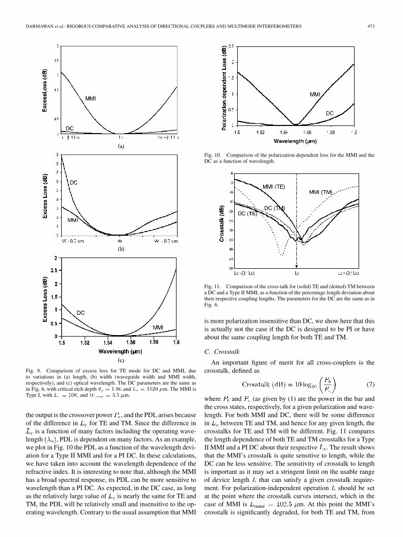
DARMAWAN et al.: RIGOROUS COMPARATIVE ANALYSIS OF DIRECTIONAL COUPLERS AND MULTIMODE INTERFEROMETERS 473
Fig. 9. Comparison of excess loss for TE mode for DC and MMI, dueto variations in (a) length, (b) width (waveguide width and MMI width,respectively), and (c) optical wavelength. The DC parameters are the same asin Fig. 6, with critical etch depth d = 1:96 and L = 1620 �m. The MMI isType I, with L = 108, and W = 3:5 �m.
the output is the crossover power , and the PDL arises becauseof the difference in for TE and TM. Since the difference in
is a function of many factors including the operating wave-length , PDL is dependent on many factors. As an example,we plot in Fig. 10 the PDL as a function of the wavelength devi-ation for a Type II MMI and for a PI DC. In these calculations,we have taken into account the wavelength dependence of therefractive index. It is interesting to note that, although the MMIhas a broad spectral response, its PDL can be more sensitive towavelength than a PI DC. As expected, in the DC case, as longas the relatively large value of is nearly the same for TE andTM, the PDL will be relatively small and insensitive to the op-erating wavelength. Contrary to the usual assumption that MMI
Fig. 10. Comparison of the polarization-dependent loss for the MMI and theDC as a function of wavelength.
Fig. 11. Comparison of the cross-talk for (solid) TE and (dotted) TM betweena DC and a Type II MMI, as a function of the percentage length deviation abouttheir respective coupling lengths. The parameters for the DC are the same as inFig. 6.
is more polarization insensitive than DC, we show here that thisis actually not the case if the DC is designed to be PI or haveabout the same coupling length for both TE and TM.
C. Crosstalk
An important figure of merit for all cross-couplers is thecrosstalk, defined as
(7)
where and (as given by (1) are the power in the bar andthe cross states, respectively, for a given polarization and wave-length. For both MMI and DC, there will be some differencein between TE and TM, and hence for any given length, thecrosstalks for TE and TM will be different. Fig. 11 comparesthe length dependence of both TE and TM crosstalks for a TypeII MMI and a PI DC about their respective . The result showsthat the MMI’s crosstalk is quite sensitive to length, while theDC can be less sensitive. The sensitivity of crosstalk to lengthis important as it may set a stringent limit on the usable rangeof device length that can satisfy a given crosstalk require-ment. For polarization-independent operation should be setat the point where the crosstalk curves intersect, which in thecase of MMI is m. At this point the MMI’scrosstalk is significantly degraded, for both TE and TM, from
474 IEEE JOURNAL OF SELECTED TOPICS IN QUANTUM ELECTRONICS, VOL. 11, NO. 2, MARCH/APRIL 2005
its minima at (different for TE and TM) because of the sen-sitivity to length. If the required crosstalk for both TE and TMis to be less than dB, for example, then the device lengthmust fall within only m of the polarization-independentpoint. This stringent requirement can be avoided only by min-imizing the difference between TE and TM. By contrast,for an ideal symmetric DC, the crosstalk is given by [cf. (1)]
, which is quite insensitive tovariations in within 10% of , and is independent of the po-larization if is the same for TE and TM. In the nonideal case,the crosstalk is degraded by any asymmetry such as when thewaveguides are not identical [6].
In conclusion, this section highlights the fact that DC, as longas it is designed to have nearly the same coupling length for TEand TM, can potentially have better performance than the MMIin terms of crosstalk and polarization sensitivity. Such a DC,however, requires careful control of many design parameters,as discussed in Section III. By contrast, the MMI is relativelysimple in design. The key to improving its crosstalk and polar-ization dependence is to minimize the difference in betweenTE and TM. In this regard, Type II is slightly better than Type Ias the difference in is smaller.
VII. EFFECTS OF HIGHER-ORDER MODES AND LATERAL
MODE FILTERING
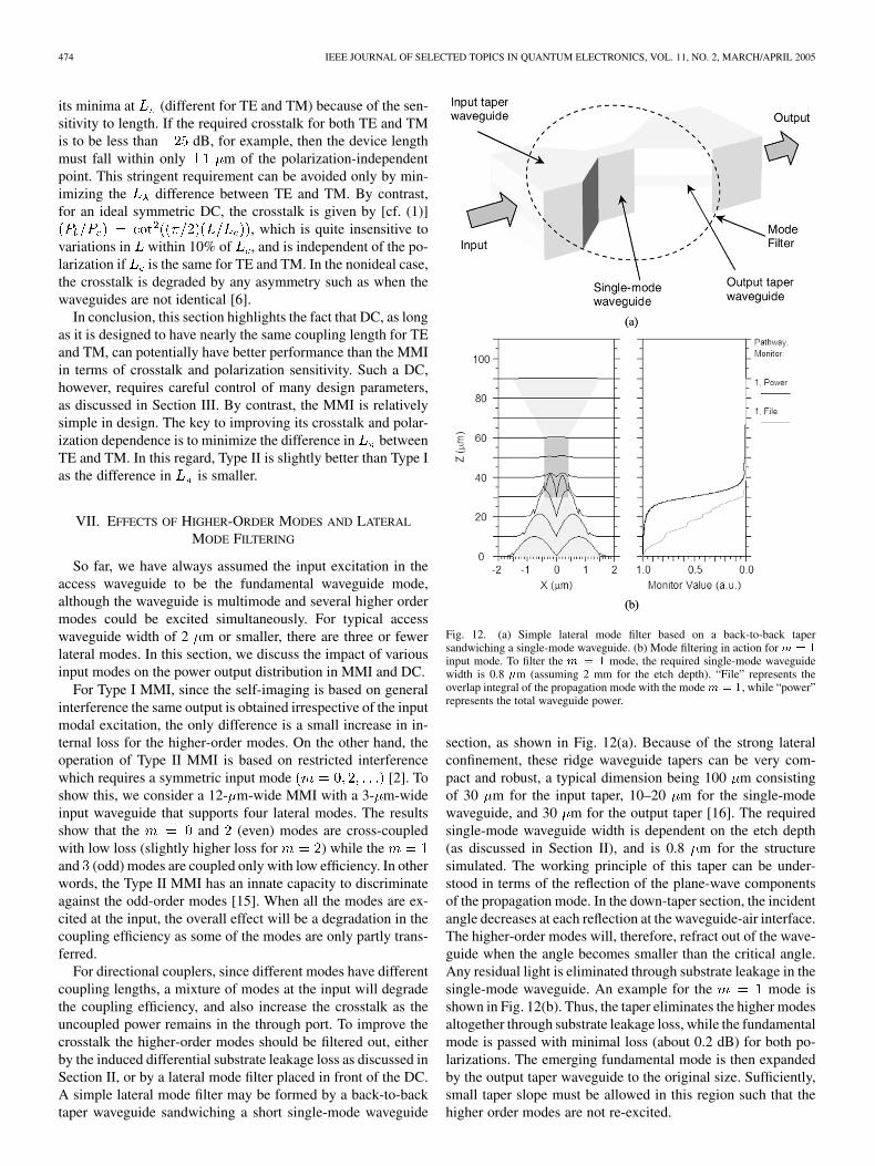
So far, we have always assumed the input excitation in theaccess waveguide to be the fundamental waveguide mode,although the waveguide is multimode and several higher ordermodes could be excited simultaneously. For typical accesswaveguide width of 2 m or smaller, there are three or fewerlateral modes. In this section, we discuss the impact of variousinput modes on the power output distribution in MMI and DC.
For Type I MMI, since the self-imaging is based on generalinterference the same output is obtained irrespective of the inputmodal excitation, the only difference is a small increase in in-ternal loss for the higher-order modes. On the other hand, theoperation of Type II MMI is based on restricted interferencewhich requires a symmetric input mode [2]. Toshow this, we consider a 12- m-wide MMI with a 3- m-wideinput waveguide that supports four lateral modes. The resultsshow that the and (even) modes are cross-coupledwith low loss (slightly higher loss for ) while theand (odd) modes are coupled only with low efficiency. In otherwords, the Type II MMI has an innate capacity to discriminateagainst the odd-order modes [15]. When all the modes are ex-cited at the input, the overall effect will be a degradation in thecoupling efficiency as some of the modes are only partly trans-ferred.
For directional couplers, since different modes have differentcoupling lengths, a mixture of modes at the input will degradethe coupling efficiency, and also increase the crosstalk as theuncoupled power remains in the through port. To improve thecrosstalk the higher-order modes should be filtered out, eitherby the induced differential substrate leakage loss as discussed inSection II, or by a lateral mode filter placed in front of the DC.A simple lateral mode filter may be formed by a back-to-backtaper waveguide sandwiching a short single-mode waveguide
Fig. 12. (a) Simple lateral mode filter based on a back-to-back tapersandwiching a single-mode waveguide. (b) Mode filtering in action form = 1
input mode. To filter the m = 1 mode, the required single-mode waveguidewidth is 0.8 �m (assuming 2 mm for the etch depth). “File” represents theoverlap integral of the propagation mode with the modem = 1, while “power”represents the total waveguide power.
section, as shown in Fig. 12(a). Because of the strong lateralconfinement, these ridge waveguide tapers can be very com-pact and robust, a typical dimension being 100 m consistingof 30 m for the input taper, 10–20 m for the single-modewaveguide, and 30 m for the output taper [16]. The requiredsingle-mode waveguide width is dependent on the etch depth(as discussed in Section II), and is 0.8 m for the structuresimulated. The working principle of this taper can be under-stood in terms of the reflection of the plane-wave componentsof the propagation mode. In the down-taper section, the incidentangle decreases at each reflection at the waveguide-air interface.The higher-order modes will, therefore, refract out of the wave-guide when the angle becomes smaller than the critical angle.Any residual light is eliminated through substrate leakage in thesingle-mode waveguide. An example for the mode isshown in Fig. 12(b). Thus, the taper eliminates the higher modesaltogether through substrate leakage loss, while the fundamentalmode is passed with minimal loss (about 0.2 dB) for both po-larizations. The emerging fundamental mode is then expandedby the output taper waveguide to the original size. Sufficiently,small taper slope must be allowed in this region such that thehigher order modes are not re-excited.

DARMAWAN et al.: RIGOROUS COMPARATIVE ANALYSIS OF DIRECTIONAL COUPLERS AND MULTIMODE INTERFEROMETERS 475
VIII. CONCLUSION
We have discussed and compared the unique characteristicsof directional couplers and multimode interferometers based onridge waveguides. The two devices are not only similar in func-tionality, but also intimately related as the MMI is derived fromthe DC. We have shown, for the first time, the continuous evo-lution from the two-mode coupling characteristic of DC to themultimode mixing and interference characteristic of MMI thataccompanies the structural transformation from DC to MMI.The resulting MMI is not only more compact than the orig-inal DC, but the same compact size can be given by two dif-ferent types of MMI based on the two different self-imagingmechanisms.
We also show that the ridge-waveguide directional couplers,under certain conditions, can be quite compact, and the couplinglength can be nearly the same for both TE and TM polarizations,as a result of the unique feature of ridge waveguides. Conse-quently, the DC can be just as polarization insensitive and broad-band as the MMI. These features, however, require the carefuldesign of a large set of design parameters. By comparison, theMMI design is more robust and involves few design variables.
These compact MMI and DC are basic building blocks withmany applications and advantages for high-density photonic in-tegrated circuits, especially if they also have the polarization in-dependent properties. As an example, they can be used as thelateral couplers for ring resonators [11], [16]. With the polar-ization independent properties of DC and MMI, along with theuse of polarization-independent waveguides, it may be possibleto design ring resonator filters that are polarization-independent[10].
REFERENCES
[1] R. A. Forber and E. Marom, “Symmetric directional coupler switches,”IEEE J. Quantum Electron., vol. QE-22, no. 6, pp. 911–919, Jun. 1986.
[2] L. B. Soldano and E. C. M. Pennings, “Optical multi-mode interferencedevices based on self-imaging: Principles and applications,” J. Lightw.Technology., vol. 13, no. 4, pp. 615–627, Apr. 1995.
[3] Y. Ma, S. Park, L. Wang, and S. T. Ho, “Ultracompact multimode in-terference 3-dB coupler with strong lateral confinement by deep dryetching,” IEEE Photon. Technol. Lett., vol. 12, no. 5, pp. 492–494, May2000.
[4] M. K. Chin, “Polarization dependence in waveguide-coupled micro-res-onators,” Opt. Exp., vol. 11, pp. 1724–1730, 2003.
[5] M. K. Chin, C. Youtsey, W. Zhao, T. Pierson, Z. Ren, S. L. Wu, L. Wang,Y. G. Zhou, and S. T. Ho, “GaAs microcavity channel-dropping filterbased on a race-track resonator,” IEEE Photon. Technol. Lett., vol. 11,no. 12, pp. 1620–1622, Dec. 1999.
[6] M. Rajarajan, B. M. A. Rahman, and K. T. V. Grattan, “A rigorous com-parison of the performance of directional couplers with multimode in-terference devices,” J. Lightw. Technology., vol. 17, no. 2, pp. 243–248,Feb. 1999.
[7] W. P. Huang, C. Xu, S. Chi, and S. K. Chaudhuri, “The finite-differencevector beam propagation method: Analysis and assessment,” J. Lightw.Technology, vol. 10, no. 3, pp. 295–305, Mar. 1992.
[8] R. J. Deri and E. Kapon, “Low loss III–V semiconductor optical waveg-uides,” IEEE J. Quantum Electron., vol. 27, no. 3, pp. 626–640, Mar.1991.
[9] J. M. Heaton, M. M. Bourke, S. B. Jones, B. H. Smith, K. P. Hilton, G. W.Smith, J. C. H. Birbeck, G. Berry, S. V. Dewar, and D. R. Wight, “Op-timization of deep-etched, single-mode GaAs/AlGaAs optical waveg-uides using controlled leakage into the substrate,” J. Lightw. Technol.,vol. 17, no. 2, pp. 267–281, Feb. 1999.
[10] M. K. Chin, C. Xu, and W. Huang, “Theoretical approach to a polariza-tion-insensitive single-mode microring resonator,” Opt. Exp., vol. 12, pp.3245–3250, Jul. 2004.
[11] Z. Bian, B. Liu, and A. Shakouri, “InP-based passive ring-resonator-coupled lasers,” IEEE J. Quantum Electron., vol. 39, no. 7, pp. 859–865,Jul. 2003.
[12] C. Themistos and B. M. A. Rahman, “Design issues of a multimodeinterference-based 3-dB splitter,” Appl. Opt., vol. 41, pp. 7037–7044,Nov. 2002.
[13] N. Yoshimoto, Y. Shibata, S. Oku, S. Kondo, and Y. Noguchi, “Designand demonstration of polarization-insensitive Mach-Zehnder switchusing a lattice-matched InGaAlAs/InAlAs MQW and deep-etchedhigh-mesa waveguide structure,” J. Lightw. Technol., vol. 17, no. 9, pp.1662–1669, Sep. 1999.
[14] P. A. Besse, M. Bachmann, H. Melchior, L. B. Soldano, and M. K. Smit,“Optical bandwidth and fabrication tolerances of multimode interfer-ence couplers,” IEEE J. Lightw. Technol., vol. 12, no. 6, pp. 1004–1009,Jun. 1994.
[15] M. Kohtoku, Y. Shibata, and Y. Yoshikuni, “Evaluation of the rejec-tion ratio of an MMI-based high order mode filter using optical low-co-herence reflectometry,” IEEE Photon. Technol. Lett., vol. 14, no. 7, pp.968–970, Jul. 2002.
[16] C. W. Lee and M. K. Chin, “Design of lateral-modes filter based on high-index contrast wave guide,” Opt. Commun., submitted for publication.
[17] D. G. Rabus and M. Hamacher, “MMI-coupled ring resonators inGaInAsP-InP,” IEEE Photon. Technol. Lett., vol. 13, no. 8, pp. 812–814,Aug. 2001.
Stevanus Darmawan (S’04) was born in Jakarta,Indonesia, in 1981. He received the B.Eng. degreein electronic and electrical engineering in 2003from Nanyang Technological University, Singapore,where he is currently working toward the Ph.D.degree in photonics.
His research interests include photonic integratedcircuits based on compound semiconductor InP.
Shuh-Ying Lee (S’04) was born in Kuala Lumpur,Malaysia, in 1979. She received the B.Eng. degree inelectronic and electrical engineering with a special-ization in photonics in 2003 from Nanyang Techno-logical University, Singapore, where she is currentlyworking toward the Ph.D. degree.
Her research interests include photonic integratedcircuits based on compound semiconductors.
Chee-Wei Lee (S’03) was born in Kuala Lumpur,Malaysia, in 1978. He received the B.Eng. degreein electronic and electrical engineering in 2003from Nanyang Technological University, Singapore,where he is currently working toward the Ph.D.degree in photonics.
His research interests include photonic integratedcircuits.
Mee-Koy Chin (S’91–M’92–SM’03) received dualB.S. degrees from the Massachusetts Institute ofTechnology, Cambridge, in 1986, and the Ph.D.degree from the University of California, San Diego,in 1992.
He is currently an Associate Professor of electricalengineering at the Nanyang Technological Univer-sity (NTU), Singapore. In 1993, he joined NTU andstarted the first photonics research laboratory in Sin-gapore. In 1997, he returned to the U.S. and workedseveral years in the photonics startup industry, before
rejoining NTU in January 2003. His research interests include integrated optics.
Copyright © 2022 FDOKUMEN