Optical impedance matching with scanning near-field optical microscopy

Opt Quant Electron (2009) 41:463–480DOI 10.1007/s11082-010-9379-x
Large capacity optical router based on arrayedwaveguide gratings and optical loop buffer
Rajiv Srivastava · Rajat Kumar Singh ·Yatindra Nath Singh
Received: 22 September 2008 / Accepted: 23 March 2010 / Published online: 8 April 2010© Springer Science+Business Media, LLC. 2010
Abstract This paper presents optical packet switch architecture with large bufferingcapacity for the contention resolution of the packets. The main feature of the architecture isno requirement of Demux/Mux and splitter/combiner which are used in most of the otherloop buffer based switch architectures. Therefore physical loss of the architecture is veryless, and switch performance is not limited by the physical degradation of the signal. In thebuffer, TWCs/SOAs are replaced by Tunable Fiber Bragg Gratings (TFBGs). The use ofTFBGs inside the buffer is a novel approach towards buffering structure. The architecturepresented here can be modeled as output queue buffer scheme. This paper investigates theadvantages of the proposed architecture over the earlier architecture. The performance of thearchitecture in terms of physical layer parameters (loss analysis, power analysis and noiseanalysis), packaging volume and optical cost is done.
Keywords Arrayed waveguide gratings · Loop buffer · Tunable fiber Bragg gratings
1 Introduction
Optical packet switching (OPS) provides connection-less networking. The major advantagesof OPS are utilization of large bandwidth of the optical fiber, data rate transparency, low loss,higher speed etc.. Photonic packet switches utilize both large capacity of the optical fiber fordata transmission and mature electronics for the control operation. Thus the growing internettraffic demands can be catered to using photonic networks. At the switching nodes in the opti-cal packet switched networks, data pass through in optical form Tucker and Zhong (1999).The control logic for these switching nodes is usually implemented in electronic domain. In
R. Srivastava (B) · Y. N. SinghIndian Institute of Technology,IIT Kanpur, Kanpur, Uttar Pradesh, Indiae-mail: [email protected]
R. K. SinghIndian Institute of Information Technology, Allahabad, India
123

464 R. Srivastava et al.
Fig. 1 Overlay structure of the network
photonic switching, data is transported in short blocks (called packets or cells) as in most ofthe currently existing electronic network like ATM (Asynchronous Transfer Mode), TCP/IP(Transmission Control Protocol/Internet Protocol) etc.. The packet contains two segments:header and payload. The header is encoded at lower bit rate, and contains information suchas source address, destination address etc.. The payload contains actual data and encoded atthe data rate ranges from a few Mbps to some tens of Gbps. The important components of aphotonic packet switch (Tucker and Zhong 1999) are control, packet routing, packet synchro-nization, clock recovery, contention resolution, buffering and packet header replacement. Inthe optical packet switching, buffering will be required when two or more packets arrive forthe same output port in same time slot. Then, one of the contending packets will be directedto the output port, and rest of them, have to be stored in random access memory (RAM). Tillnow, all optical RAMs for photonic packet switching has not yet been developed. For thecontention resolution, three solutions can be used:
1. Fiber delay lines (FDL) in traveling and recirculating configuration in time domain;2. Deflection routing in space domain; and3. Wavelength conversion of the data in wavelength domain.
At the input of the switch, packets can arrive synchronously or asynchronously and the arriv-ing packet may be of same or variable lengths. It has been found in previous study thatswitches, at which packets of equal lengths arrive synchronously, have better performance.Furthermore, recently Tucker (2008) has shown that optical components don’t have muchadvantage over electrical components in term of power consumption some time; they con-sume even more power (Tucker 2008). Thus, it is believed that hybrid scheme; in which corenetwork is optical in nature while edge routers will be electronic in fashion, is the betterchoice (Yoo 2003). The overlay structure of the network is shown in Fig. 1. The networkis composed of edge and core routers. The Edge routers act as an interface between clientsand core network. The core routers are optical, while edge routers are electronic in nature.The control operation of the core and edge routers is performed by the electronics. The edgerouters placed at the boundary of the network are capable of packet aggregation. The ingressedge router receive packets from the client network and converts it in appropriate format and
123

Large capacity optical router based on arrayed waveguide gratings 465
directs the aggregated packet towards core routers. The electronic edge router is assumedto include electronic RAM’s, optical TDM and switch fabric for buffering, aggregation andforwarding of packets. The backbone networks, where large numbers of aggregated datapackets flows at a very high data rate will be optical in nature. As discussed above, the corerouters are designed for the equal length packets and the length of the packet is assumedto be equal to one slot duration. This network architecture takes the advantages of both theoptical and the electronic domains (Yoo 2003).
Many optical packet switch architectures for the core network have been reported in lit-erature (Bendelli 1995; Choa 2005). All of them have their advantages and disadvantages.The first loop buffer based architecture was proposed by Bendelli (1995). This architecturerequires a very large number of components for buffering; semiconductor optical amplifier(SOA), and also the size of the demux and mux effectively scales linearly with requirednumber of buffer wavelengths. Thus physical loss of the architecture is very large. The mainlimitations of the SOA based architecture are:
1. Simultaneous read/write operation is not possible, as SOA used as ‘gate switch’ and ithas to be turned ‘ON’ and ‘OFF’ and both of these operations cannot be performed insingle time slot.
2. Dynamic re-allocation of wavelengths is not possible.3. Dynamic range of SOA is limited.4. Crosstalk due to SOA is very high.
The above mentioned limitations can be mitigated using tunable wavelength converter(TWC), in place of SOA in the buffer (Verma et al. 2002; Singh et al. 2003). However,the TWC also has following limitations:
1. With the current technology the tuning range of the TWC is very limited.2. Commercialized TWC are noisy device, and hence signal quality degrades when wave-
length is tuned (InPhenix/products (available at; http://www.inphenix.com/)).
The architecture proposed by Choa (2005) have similar buffer structure as in Ref. Bendelli(1995), but the physical loss in the buffer is less. hence, signals received at the switch outputhave better signal quality. However, in this architecture direct packets which require no delayalso pass through the buffer demux. Thus scaling is more difficult in this architecture. Thecomparative study of the loop buffer based architecture is made in Ref. Srivastava et al.(2008), and it is shown that TWC based architectures outperforms the SOA based architec-tures. The detailed physical layer analysis of TWC based loop buffer architecture is performedin Ref. Srivastava et al. (2009).
In Ref. Chia et al. (2001), array waveguide grating (AWG) based architecture as shownin Fig. 2 has been proposed. This architecture consist of AWG router as core of the switchand fiber loop buffer module for the storage of the packets. It takes the advantages of AWGrouters, low insertion loss, wavelength domain routing and large buffering capacity of thefiber loop buffer. This architecture provides low packet loss probability, but the problemsassociated with this architecture are as follows:
1. In each buffer module demux and mux are used, and in between them traveling type fiberdelay lines are used. These fiber delay lines are of integral multiple of slot durations.Thus, the architecture is bulky in nature and physical degradation in signal quality islarge.
123

466 R. Srivastava et al.
Fig. 2 Schematic of architecture A1 and buffer module
2. Exit time contention may occur. This is explained in Ref. Chia et al. (2001).3. The author presents architecture for the non blocking optical time slot inter-changer
(OTSI, structure of parallel delay lines of variable length), no attention is paid on block-ing OTSI.
In past, to exploit the advantages of both the architectures (loop buffer and AWG based),an architecture is proposed (Singh et al. 2007), where loop buffer based architecture is usedfor the buffering, and AWG based architecture for the routing of the packets is used. Thisarchitectures also suffers from a few limitations as explained:
1. TWC is used in the buffer, and hence above mentioned limitations will also be there.2. As SOA/TWC controls each wavelength separately splitter/demux and combiner/mux
are used in the buffer, and hence buffer becomes lossy and bulky.
Here, we have proposed the use of tunable fiber Bragg gratings (TFBGs) inside the buffer,then there will be no need of the components like mux/demux and splitter/combiner to formthe buffer. Hence, physical loss of the architecture reduces to large extent, and more numberof re-circulations is possible as shown in Ref. Srivastava et al. (2008). However, with TFBGssimultaneous read/write operation is not possible. Still this will not impose any limitationson the architecture, and it will be discussed in the section-3 of the paper. Hence, the completeswitch will composed of tunable fiber Bragg gratings based loop for the buffering of packets,and AWG router for the routing of the packets.
As most of the tunable optical components are not commercially available, hence for thefeasibility of the architectures it is necessary to discuss the current status of the components,as made in next subsection.
1.1 Current status of the tunable components
1.1.1 Tunable wavelength convertor and tunable filter
Tunable wavelength convertor and Tunable filter have been used in the various optical packetswitch architectures for last two decade without considering their switching time limitations.The wavelength conversion in optical domain can be obtained through the phenomenon ofcross phase modulation, cross gain modulation and four wave-mixing in SOA. SOA based
123

Large capacity optical router based on arrayed waveguide gratings 467
TWC and TF which utilizes the phenomenon of quantum well intermixing have been reportedrecently (Choa 2005), which can be tuned within few nano-second. Thus, with existing tech-nology, these two devices will not put any constraint on the switch performance and recentlythese two components are commercialized by ‘InPhenix’ an optical components manufac-turering company.
1.1.2 Tunable fiber Bragg gratings
Fiber gratings are developed by the exposure of UV light on the small piece of fibers. There arenumber of ways by which gratings can be tuned. These techniques include thermal heating,mechanical stress, chemical and electro-optical phenomenon. All these techniques changethe optical distance between adjacent grating fringes. The most commonly used methodsfor grating tuning are heating and mechanical compression. But these are slow tuning pro-cesses and works only in kilohertz region. A TFBG based N × N optical cross connect hasbeen reported in Kim (2002), where tunability is achieved by strain effect, and assumed thatswitching time of the TFBG do not put any constraint. With current technology, switch-ing time of some tens of microseconds is achievable. However, electro-optic methods havepotential to work in the gigahertz region. The optical fiber generally consists of fused silicaglass that lack second order nonlinear susceptibility. Therefore, it is not possible to obtainany electro-optic effect in the fiber. However, it has been shown that thermal polling cangenerate second order nonlinearity and can be used for the tuning purpose (Myren 2005).Thus, currently intense research is going on in this area, and tunable fiber Bragg gratingswith fast tunability are expected to be available soon. Therefore, we have assumed that thetuning speed of the TFBG don’t put any constraint on the switch performance. The otherimportant issue associated with TFBG is reflectivity. As mention in Ref. Kim (2002), reflec-tivity of 99.7% is achievable. Thus the transmission is −27 dB, which is good enough for thephotonic switching applications.
The paper is organized as follows: In Sect. 2, description of the architectures is given.The working of the architectures is explained in Sect. 3. Physical layer analysis is presentedin Sect. 4. Simulation results in terms of packet loss probability are presented in Sect. 5.Packaging volume for the buffer unit is compared in Sect. 6. Optical cost comparison is donein Sect. 7. Finally, Sect. 8 concludes the paper.
2 Description of the architectures
In this paper, two architectures are presented with some distinctions. In the first configuration(Fig. 3), the switching section consists of space switch fabric. In the second configuration(Fig. 4), the space switch is replaced by the combination of TWC and AWG. Both the configu-rations have their advantages and disadvantages. In the first configuration, control complexityis Θ(NlogN ) or using sterling formula Θ(ΩlogN !) and in the second configuration, controlcomplexity is Θ(N ). Space switch used in configuration A2 is more cost effective but leadsto more control complexity. Overall performance of both the switches in terms of packetloss probability will remain the same as queuing model is same. This core of the switch isarrayed waveguide gratings (AWG) router of size 2N × 2N (Fig. 3). The upper N ports ofthe AWG ranges from 1 to N are used for connecting N buffer modules. If the performanceof the switch is optimized for M(M < N ) modules then N − M upper ports of the AWG willbe left free. The lower N ports ranging from N + 1 to 2N of the AWG router are the actualinputs/outputs ports. The lower ports are equipped with TWC which tunes the wavelength of
123

468 R. Srivastava et al.
Fig. 3 Schematic of architecture A2 and buffer module
Fig. 4 Schematic of architecture A3 and buffer module
the incoming packets as per the decision of the controller, either to place them in the bufferor to direct them to appropriate output ports. In each module, N packets can be stored onN different wavelengths using WDM technology. This allows storage of M N packets in allthe modules together. The maximum value of M is N. In the architecture, different buffermodules are independent of each others. Therefore, same set of wavelengths can be usedin all the buffer modules for the buffering of packets. Each buffer module consists of 3 dBcoupler, set of TFBGs, EDFA to compensate the loss, and an isolator. In the buffer, numberof TFBGs are equal to the number of outputs. This allows erasing of at most N packets fromthe buffer, in any time lot.
The packets can be placed in appropriate buffer module; by tuning their wavelengths fol-lowing the routing pattern of AWG. In Fig. 5, structure and routing pattern of the AWG (size8 × 8) and sets of used wavelengths for different types of routing is shown. Upper four portsare used for connecting different buffer modules and lower four ports are used as inputs/outputs ports. It can be observed from figure, that between two consecutive buffer modulesthere are N − 1 common wavelengths. Thus in M buffer modules, M + N − 1 wavelengths
123
Large capacity optical router based on arrayed waveguide gratings 469
Fig. 5 8 × 8 optical router and its routing pattern
are required. Hence, total number of wavelengths used by the switch are (N )+ (M + N −1),where N wavelengths are used for the direct transfer of packets. For example in Fig. 5, it canbe visualized that λ4 is not used in buffer and thus 4 + 4 − 1 = 7 wavelengths have beenused. Due to the symmetric nature of the AWG, if a packet arrives at the jth input port of theAWG and placed in the buffer, then it will be erased from the buffer after required amountof delay and will appears at the same jth output port of the AWG. It is evident from the darkshaded region.
3 Working of the architectures
The TWCs at the input of the switch are tuned in each time slot either to place packets in thecorresponding loop buffer module or to direct them to the appropriate outputs. The packetcan be directly transmitted to the output by tuning the wavelength of the incoming packet tothe appropriate output port wavelength by following routing pattern of the AWG as shown inFig. 5. The packets can be placed in the buffer by tuning wavelength of the incoming packetsto the corresponding output ports of AWG to which appropriate buffer module is connected.Once a packet is placed in the loop buffer, it will keep on circulating in the loop. In each passthrough the 3 dB coupler, half of the power of different wavelengths again passing throughthe scheduling AWG will appear at the input of the different tunable filters by following therouting pattern of the AWG, and other half of the power will remain in the buffer. TFs willallow only one wavelength in each slot to pass through them. In the same slot, correspondingTFBG inside the buffer is tuned to that particular wavelength (which is allowed by TF) thiswavelength gets reflected and absorbed by the isolator. Thus, packet is erased from the buffer.Afterwards, TWC at the input of the switching section (Fig. 4) tunes the wavelength of thatpacket by following the routing pattern of the switching AWG to the appropriate output port.If space switch is used (Fig. 3), then it switches the filtered packet to appropriate output port.
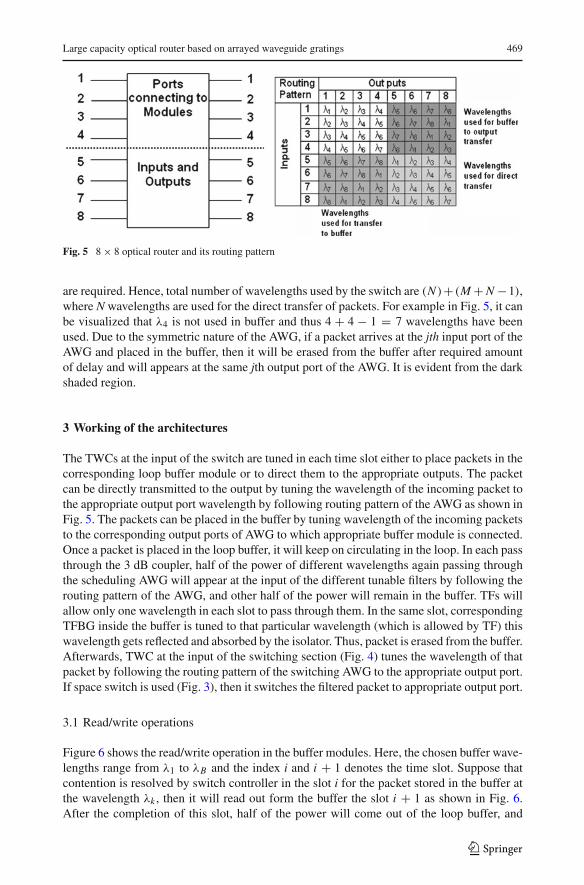
3.1 Read/write operations
Figure 6 shows the read/write operation in the buffer modules. Here, the chosen buffer wave-lengths range from λ1 to λB and the index i and i + 1 denotes the time slot. Suppose thatcontention is resolved by switch controller in the slot i for the packet stored in the buffer atthe wavelength λk , then it will read out form the buffer the slot i + 1 as shown in Fig. 6.After the completion of this slot, half of the power will come out of the loop buffer, and
123
470 R. Srivastava et al.
Fig. 6 Read/Write operation in the buffer modules
as per the desired output the respective tunable filter (TF) will tune its wavelength to λk toaccept the packet from the loop buffer. As at the beginning of the (i + 1)th slot half of thepower at wavelength λk will remain in the loop and to remove the packet from the buffer,corresponding TFBG will tune its wavelength in the beginning of the slot i + 1 to λk , andreflected power will absorb by the isolator, and at the completion of (i +1)th slot, wavelengthλk will be erased from the buffer as shown in Fig. 6. Thus in the (i + 1)th slot, no packetwill be written into the buffer at wavelength λk . This is possible after one time slot i.e., in thebeginning of (i + 2)th time slot. This constraint will not affect system performance becausethe arriving packets will follow the routing pattern of AWG, and in each module, in a singletime slot, only one packet will be stored on a single wavelength.
3.2 Advantages
The main feature of the architecture is that the demux and splitter are not required inside thebuffer unit. This is the main difference with most of the earlier loop buffer based architec-tures (Bendelli 1995; Chia et al. 2001). In the proposed architecture, as buffer is recirculatingtype then there will not be any exit time contention, as in Choa (2005). In case of exit timecontention, except one packet, other packets can be delayed for more time. This in contrastwith earlier architecture (A1) where only fixed delays are provided and it cannot be changedonce packets are placed in the buffer. As buffer is re-circulating in nature, and hence vari-ous delays are possible in each module ranges form 1 to K, where K is maximum possibleallowed re-circulations. Therefore, as per the requirements packets can be stored in any ofthe modules.
3.3 Control algorithm of the switch
1. If there are i [1 ≤ i ≤ min(M, K ) (where, M is the number of modules)] packets in allthe buffer modules for the output j, then one of them will be send to the output. If in thatslot, one or more packets for the output j are also present at the inputs, then these will bebuffered in any of the modules to the extent allowed by the step 4.
2. Considering the case when there is no packet in any of the buffer module for the outputj, but m input lines have packets for that output. Then, one of these m packets is directlysent to output j. The remaining m−1 packets will be buffered in the respective buffermodule to the extent allowed by the step 4.
3. In each buffer module, only one packet will be stored for a particular output port. Hence,in M modules at maximum M number of packets can be stored for a particular output port.
123

Large capacity optical router based on arrayed waveguide gratings 471
4. Total number of stored packets X j for a particular output in all the buffer modules cannever be greater than min(K , M), i.e.,
∑X j ≤ min(M, K ) for j = 1 · · · N .
5. In each time slot, only one packet can be erased from the buffer modules for a particularoutput.
6. Number of stored packets in the each buffer module should never be greater than N.
In the above mentioned algorithm each output has a separate queue with maximum queuelength, equal to min(M,K) slots. This can be modeled by an output queued switch. In order tomeasure the effect of maximum number of allowed re-circulations on the packet loss proba-bility, the power budget analysis is presented in the next section. Later on simulation resultsare presented in Sect. 5.
4 Physical layer analysis
In this section, physical layer analysis in terms of loss, power and noise is presented. Subse-quently, OSNR (optical signal to noise ratio) is measured, and maximum number of allowedre-circulations are evaluated such that the BER (bit error rate) level is below 10−9. In thefollowing section, the switch A(1), A(2) and A(3) is denoted as A(z), here z ε (1,2,3).
4.1 Loss analysis
For the mathematical ease, switch can be divided into three parts as input unit, buffer unitand output unit. The loss of input unit which consist of TWCs and AWG (same in eacharchitecture) is given by
Ain(z) = AT WC AscAW G z ε [1, 2, 3] (1)
The loss of loop buffer unit in architecture A1 can be calculated as
AL(1) = AscAW G AT WC AM AD AT WC (2)
The loss of loop buffer unit in architecture A2 and A3 can be calculated as
AL(2, 3) = A3 d B AI so(AT F BG)N A3 d B (3)
If data remain in the buffer of K number of re-circulations, then the total loss suffered bypacket in the loop buffer can be written as ALoop= [AL(z)]K . Similarly the loss of output unitin different architectures can be obtained as
Aout(1) = AT WC ASS (4)
Aout(2) = AscAW G AT F ASS (5)
Aout(3) = AscAW G AT F AT WC Asw
AW G (6)
By combing all the above losses, total loss of the different switch architectures can be writtenas
AT (z) = Ain(z)[AL(z)]K Aout(z) (7)
4.2 Power analysis
In this sub-section power analysis is presented. Here, an expression is presented to evaluatethe maximum number of allowed re-circulations (K) of the data stored in the buffer.
123

472 R. Srivastava et al.
4.2.1 Without EDFA
In the first case, we are assuming that in all the architectures erbium doped fiber amplifier(EDFA) is not placed in the buffer, and hence power of the signal (Ps) after K re-circulationsfor bit ‘b’ in different architectures will be given by:
Ps(K , z) = bPin Ain(z)[AL (z)]K Aout(z) b ε [0, 1] (8)
where, Pin is the input signal power. The extinction ratio ε = [P(1)/P(0)] is assumed to beinfinite.
4.2.2 With EDFA
Here, we are assuming that, in each architecture EDFA is placed in the buffer to compensatethe loop loss. Here, the calculation is somewhat involved, and can be detailed as:
Power entering the loop buffer for bit b is
Ps,z = bPin Ain(z) b ε [0, 1] (9)
The signal power after first circulation will be
Ps(1, z) = Ps,z AL(z)G1,z + nsp(G1,z − 1)hνB0. (10)
In the above equation, the second term [nsp(G1,z −1)hνB0] represents the ASE noise poweradded to the signal in the first circulation (Olsson 1989). Considering the fact that, the dataremain in the buffer for K number of re-circulations. Then, TFBG inside the buffer willremain transparent for first (K − 1)th re-circulations and tunes the wavelength in the Kthcirculation. Thus, the power of the signal after K − 1 and K circulations for bit b is given by
Ps(K − 1, z) = Ps(K − 2, z)AL (z)G K−1,z + nsp(G K−1,z − 1)hνB0. (11)
and
Ps(K , z) = Ps(K − 1, z)AL (z)G K ,z + nsp(G K ,z − 1)hνB0. (12)
respectively. As the gain of the EDFA in each architecture is constant and independent ofnumber of re-circulations, and hence above equation can be simplified to
Ps(K , z) = bPin Ain(z)[AL(z)G(z)]K + nsp(G(z) − 1)hνB0 F (13)
Here,
F =1−[AL (z)G(z)]K
1−AL (z)G(z) AL(z)G(z) < 1K AL(z)G(z) = 1
(14)
For the maximization of SNR the gain loss product (AL(z)G(z)) should be equal to one(Naik and Singh 2002), Eq. 13 can be simplified as,
Ps(K , z) = bPin Ain(z) + nsp(G(z) − 1)hνB0 K . (15)
In both the cases, power at the output of the switch is
Pout(K , z) = Ps(K , z)Aout(z). (16)
123
Large capacity optical router based on arrayed waveguide gratings 473
4.3 Noise analysis
4.3.1 Without EDFA
Here, we have assumed that EDFA is not placed in the buffer. Therefore, there are only twonoises i.e., shot and thermal noise. Hence,various noises terms are given by
σ 2s = 2q R P(K , z)Be, (17)
σ 2th = 4K B T Be
RL.
where,
P(K , z) = bPin Ain(z)[AL (z)]K Aout(z) (18)
4.3.2 With EDFA
Here, we have assumed that EDFA is placed in the buffer to compensate the loss of theloop buffer. This amplifier not only amplify the signal but also add amplified spontaneousemission (ASE) noise to the signal. Due to the square law detection by the photo-detectorof receiver, various noise components are generated by the beating. These noise componentsare shot noise, ASE-ASE beat noise, sig-ASE beat noise, ASE-shot beat noise and thermalnoise with variances given by Olsson (1989), and denoted by σ 2
s , σ 2sp−sp, σ 2
sig−sp, σ 2s−sp
and σ 2th respectively. These noise variances for bit ‘b’, after performing K re-circulations,
are given by
σ 2s = 2q R P(K , z)Be,
σ 2sp−sp = 2R2 P2
sp(K , z)(2Bo − Be)Be
B2o,
σ 2sig−sp = 4R2 P(K , z)
Psp(K , z)Be
Bo, (19)
σ 2s−sp = 2q R Psp(K , z)Be, and
σ 2th = 4K B T Be
RL.
The expression for P(K) and Psp(K ) will be given by
P(K , z) = bPin Ain(z)Aout(z) and Psp(K , z) = K nsp[G(z) − 1]hνB0 Aout(z) (20)
The total noise variance for bit ‘b’ will be
σ 2(b) = σ 2s + σ 2
sp−sp + σ 2sig−sp + σ 2
s−sp + σ 2th (21)
Under the Gaussian approximation the bit-error rate (Olsson 1989) can be obtained as
B E R = Q
(I (1) − I (0)
σ (1) + σ(0)
)
(22)
where Q(x) is known as the error function and is defined as
Q(x) = 1√2π
∞∫
x
exp(−x2/2)dx (23)
123

474 R. Srivastava et al.
Table 1 List of different parameters
R Responsivity 1.28 Amp/Watts
nsp Population inversion factor 1.1
h Planck’s constant 6.6 × 10⁻³⁴ J-s
c Speed of light 3 × 10⁸ m/s
Be Electrical bandwidth 10 GHz
Bo Optical bandwidth 20 GHz
q Electronic charge 1.6 × 10⁻¹⁹ Coulomb
RL Load resistance 300 Ω
T Temperature 300 K
K B Boltzmann constant 1.38 × 10⁻²³ J/K
A3d B 3 dB coupler loss 3.0 dB
AAW G AWG loss (W × W ) 1.5(Log2 W−1) dB
Ass Space Switch loss (1 × W ) 10(Log10 W ) dB
AM/D Mux/Demux loss (1 × W ) 1.5(Log2 W−1) dB
AT WC TWC loss 2 dB
AT F Tunable filter loss 2 dB
AT F BG Tunable fiber Bragg grating loss 0.2 dB
AI so Isolator loss 0.15 dB
Table 2 Maximum number of allowed re-circulations at different power levels (without EDFA) for switchsize N = 4, and buffering of 4 packets in each module
Switch P = 10 µW P = 20 µW P = 50 µW P = 100 µW
K K K K
A1 1 2 2 2
A2 2 2 3 3
A3 1 2 3 3
The terms I (1) = R P(1) and I (0) = R P(0) are photocurrent, sampled by the receiverduring bit ‘1’ and bit ‘0’ respectively. System model discussed above is used for calculatingmaximum allowed re-circulations. The values of the different parameters used in the calcu-lations are given in Table 1. The loss formula used for the demux, mux and AWG is fittedformula, and its is reasonably ok for W ≤ 16. For a particular case of interest, the signalpower of each of the channels is assumed to be same. The acceptable BER is consideredto be less than 10−9. The maximum number of allowed re-circulations at different powerlevels for the various architectures, without and with EDFA is presented in Tables 2 and 3respectively. It can be summarized for the Table 2, if EDFA is not placed in the buffer, then allthe considered architectures suffer form re-circulation limits. Moreover, maximum numberof allowed re-circulations cannot be increased using higher power levels. In contrast to this,once EDFA is placed in the buffer, such that it compensate the loop loss. The architecture A2,A3 becomes free form re-circulation limits. However, the architecture A1, suffers form there-circulation limits at the power levels of 10 µW. In the buffer, two scenarios can arise, in thefirst scenario, each packet can stay in the buffer for K < M number of re-circulations, wherearchitecture suffers form the re-circulation limits. In the second case, each packet can stay
123

Large capacity optical router based on arrayed waveguide gratings 475
Table 3 Maximum number of allowed re-circulations at different power levels (With EDFA) for switch sizeN = 4, and buffering of 4 packets in each module
Switch P = 10 µW P = 20 µW P = 50 µW P = 100 µW
K K K K
A1 3 10 16 33
A2 7 22 37 75
A3 6 21 36 74
Table 4 Maximum number of allowed re-circulations at different power levels (with EDFA) for switch A2of size N = 4, and buffering of 4 packets in each module
Switch P = 3 µW P = 5 µW P = 7 µW P = 10 µW
K K K K
A2 1 3 4 7
in the buffer for M number of re-circulations. This happens when K ≥ M . In this case, therewill be no effect of the circulation limits. Overall, the performance of the architecture A2is better in comparison to other considered architectures. The other important point is that,once the maximum number of allowed recirculations are more than the maximum allowedbuffering capacity, architecture is free from re-circulation limits, and there is no meaning todesign an architecture which allows very high number of re-circulations. However, this isnot the case, because of following reasons:
1. As the size of the switch increases, the maximum number of allowed re-circulationsdecreases in a very fast manner, and hence the architectures which allow more numberof re-circulations are easily scalable.
2. In prioritized traffic, a packet can remain in the buffer, for longer duration (K � M).However, it depends on the scheduling algorithm.
3. While using switch as optical memory, a large number of re-circulations are needed,without deteriorating much signal power.
5 Simulation results
Hence, it can be observed from the Table 4 that if the signal power is below 7 µW, therewill be re-circulation limits, and the allowed buffer capacity can not be utilized effectively.Hence, once the switch size increases, the minimum power also increases, to overcome there-circulation limits. But this is not straightforward, as signal power increases, the non-lineareffects starts to dominate, and re-circulations again falls (Srivastava et al. 2009). Hence, inthe simulation results the effect of re-circulation limits should to taken into account to exactlymeasure the switch performance in terms of packet loss probability. In the algorithm detailedin Sect. 3 each output has a separate queue with maximum queue length, equal to min (M, K )slots. This can be modeled by an output queued switch.
5.1 Random traffic model
The random traffic model is simple; still it provides good insight of the architecture. Thismodel assumes that packets can arrive at any of the inputs with probability p and each packet
123

476 R. Srivastava et al.
Table 5 Optical cost of the components in terms of FCC
Symbol Description Cost
CD(W ) Cost of demultiplexer (W channels) W + 1
CM (W ) Cost of multiplexer (W channels) W + 1
CS/AW G (I, O) Cost of switch/AWG (I/O input/output ports) I+O
CE DF A Cost of EDFA 2
CT F Cost of tunable filter 2
CI so Cost of Isolator 2
C3d B Cost of 3 dB coupler 4
CT WC Cost of TWC 4
CT F BG Cost of tunable fibre Bragg grating 2
CF Cost of fibre 2
is equally likely to be destined to any one of the outputs with probability 1/N. Thus theprobability that K packets arrive for a particular output in any time slot is given by
P(K ) = N CK
( p
N
)K (1 − p
N
)N−K(24)
The queuing model for the output queued switch is given in Karol et al. (1987), Hluchyjand Karol (1988), and using the same model, performance of the output queued system underthe random traffic condition is shown in presented in Srivastava et al. (2007), hoverer, in theanalysis effect of the re-circulation limit is not considered. Here, in the Fig. 7. the effect ofre-circulation limits is shown, and it can be observed that the re-circulation limits have deepimpact on the overall performance of the switch. Comparing the data at the load of 0.6, thepacket loss is 100 times lesser in case of K = 4 in comparison to K = 2. In the architectureoutput queue is formed in wavelength domain, therefore while scaling there will less incre-ment (only more TFBGs are required) in the hardware in contrast to architecture A1, wheresize of OTSI has to be increased. In architecture A1, this is where problem lies, because assize of the OTSI increases the maximum allowed re-circulations will decrease, and TWCswill not be able to handle large number of packets and exit time contention will become moresevere. Hence, scaling is very critical in architecture A1.
6 Minimum packaging volume for the buffer unit
In this section, the proposed architecture A2 is compared with earlier architecture A1, interms of packaging volume. Here in the comparison, only volume of the buffer unit is con-sidered, because rest of the structure is common in both the architectures. Still the packagingvolume of remaining devices can be added separately. The length of the loop is taken to beequal to one slot duration. The packet format is assumed to be same as in KEOPS project(Guillernot 1998). Thus the slot duration (T) is 1.646 μs, and the length equivalent is
L1 = c
nT (25)
123

Large capacity optical router based on arrayed waveguide gratings 477
0.2 0.4 0.6 0.8 110
−8
10−6
10−4
10−2
100
Load
Pac
ket
Lo
ss P
rob
abili
ty
K=1K=2K=3K=4
Architecture A2
Fig. 7 Packet loss probability versus load for switch size N = 4 and with maximum allowed buffering of 4packets under different number of re-circulations (K )
The length of the loop for a given size of packet can be calculated using
L = cb
nBR(26)
Here, b is the total number of bits in a packet including guard bands, BR is bit rate, and n isrefractive index of fiber. The length of the fiber used in a single buffer module in the earlierarchitecture (A1) is
L1 = B(B + 1)c
2nT (27)
The total length of the fiber used in M modules will be
L = M B(B + 1)c
2nT (28)
The total length of the fiber used in M modules in architecture A2 is
L2 = Mc
nT (29)
The Packaging volume can be calculated as,
Vi = πr2 Li i ε [1, 2] (30)
The packaging volume for earlier architecture (A1) is
V1 = πr2 M B(B + 1)cT
2n(31)
The packaging volume for the proposed architecture (A2) is
V2 = πr2 McT
2n(32)
123

478 R. Srivastava et al.
Fig. 8 Packaging volume vs. number of buffer wevelengths in architecture A1 and A2
The ratio of the volumes can be expressed as,
V1
V2= B(B + 1)
2(33)
The packaging volume for both of these architectures is shown in Fig. 8. It can be observedfrom the figure, packaging volume of the proposed architecture is independent of the numberof buffer wavelengths used for the buffering of the packets. But in the earlier architecturethe packaging volume is proportional to the B2/2. Therefore there is large reduction of thepackaging volume in the proposed architecture (Fig. 8).
7 Optical cost comparison
The optical cost of the architecture provides an estimate of hardware complexity. If the opti-cal cost is higher then the architecture is non-scalable, because higher costs indicate thateither large size components or more number of components are used. The optical cost ofthe architectures is evaluated by adding cost of each of the components used in the switchdesign. The optical cost of the individual components is obtained by counting the number offiber- to -chip coupling (FCC) (Caenegem 2006). FCC is the number of interconnection tothe outer world from that component. However, this method is entirely heuristic based and itonly count for the number of fibers that are attached to a particular component, but still thismodel is used for the comparison of the different architectures, as a rough estimate can beobtained and on that comparison can be made. The optical cost of the different componentsis shown in Table 5.
Optical cost of the architecture A1 is
CA1 = NCT WC + CAW G(2N × 2N ) + MCMod + NCT WC + CSS(N × N ) (34)
CA1 = 4N + (2N + 2N ) + MCMod + 4N + (N + N ) = 14N + MCMod (35)
123

Large capacity optical router based on arrayed waveguide gratings 479
The cost of the each buffer module can be expressed as,
CMod = CT WC + CD(1 × B) + BCF + CM (B × 1) + CT WC (36)
CMod = 4 + (1 + B) + 2B + (B + 1) + 4 = 10 + 4B (37)
Thus the cost of the architecture A1 is
CA1 = 14N + 4B M + 10M (38)
Optical cost of the architecture A2 is
CA2 = NCT WC + CAW G(2N × 2N ) + MCMod + NCT F + NCT WC + CSS(N × N )
(39)
CA2 = 4N + (2N + 2N ) + MCMod + 2N + (N + N ) = 14N + MCMod (40)
The cost of the each module is
CMod = C3d B + NCT F BG + CI SO + CE DF A + CF (41)
CMod = 4 + 2N + 2 + 2 + 2 = 10 + 2N (42)
The total cost of the architecture A2 will be given by
CA2 = 14N + 2M N + 10M (43)
Similarly the optical cost of the architecture A3 will be given by,
CA3 = 16N + 2M N + 10M (44)
Considering N = 4 and M =B= 4, the cost of the architectures A1, A2 and A3 is 160 units,128 units and 136 units respectively. hence, architecture A2 is more cost effective.
8 Conclusions
In this paper AWG and TFBG based architectures are presented for photonic packet switch-ing. In these architectures once the wavelength of the packet is tuned by input TWC, it willreach to the output within bounded delay. The comparison of the proposed architectures ismade with the earlier architecture. The results presented in the paper, clearly suggest thatthe physical layer analysis is an important part in the switch design, and allowed bufferingcapacity may not be fully utilized due to the re-circulation limits. The performance of thebuffer can be improved by placing EDFA to compensate the loss of the buffer components.The effect of re-circulation limit on the packet loss probability is shown. The performance ofthe switch is measured in terms of packaging volume and optical cost. Packaging volume ofthe proposed architectures is lesser as compared to the existing architecture. The optical costof the architecture A1 is 160, which is higher as compared to the cost of the architectures A2(128) and A3 (136).
References
Bendelli, G. et al.: Photonic ATM switch based on multi-wavelength fiber loop buffer. Optic. Fiber Commun.(OFC’95) 8, 141–142 (1995)
Choa, F.S. et al.: An optical packet switch based on WDM technologies. J. Lightw. Technol. 23, 994–1013 (2005)
123

480 R. Srivastava et al.
Chia, M.C. et al.: Packet loss and delay performance of feedback and feed- foreward arrayed-waveguidegratings- based optical packet switches with WDM inputs–outputs. J. Lightwave Technol. 19, 1241–1254 (2001)
Caenegem, R.V.: From IP over WDM to all-optical packet switching: economical view. J. Lightwave Tech-nol. 24, 1638–1645 (2006)
Guillernot, C. et al.: Transparent optical packet switching: the European ACTS KEOPS project approach.J. Lightwave Technol. 16, 2117–2134 (1998)
Hluchyj, M.G., Karol, M.J.: Queuing in high performance packet switching. IEEE J. Selected Areas Com-mun. 6, 1587–1597 (1988)
Kim, S.: Bidirectional optical cross connects for multiwavelength ring networks using single arrayed wave-guide grating router. J. Lightwave Technol. 20, 188–194 (2002)
Karol, M.J., Hluchyj, M.G., Morgan, S.P.: Input versus output queuing on a space-division packet switch. IEEETrans. Commun. 35, 1347–1356 (1987)
Myren, N.: Polar fiber devices. Ph.d. Dissertation TRITA-FYS 2005:22, ISSN 0280-316X, ISBN 91-7178-053-x (Royal Institute of Technology, Stockholm) (2005)
Naik, M., Singh, Y.N.: Simulation of fiber loop buffer memory of all-optical packet switch. In: Proceedingsof NCC’2002, pp. 50–54. IIT Mumbai 26–27 Jan (2002)
Olsson, N.A.: Lightwave systems with optical amplifiers. J. Lightwave Technol. 7, 1071–1082 (1989)Singh, Y.N., Kushwaha, A., Bose, S.K.: Exact and approximate modeling of an FLBM-based all optical
packet switch. J. Lightw. Technol. 21, 719–726 (2003)Srivastava, R., Singh, R.K., Singh, Y.N.: WDM based optical packet switch architectures. J. Optic. Netw. 7,
94–105 (2008)Srivastava, R., Singh, R.K., Singh, Y.N.: Design analysis of optical loop memory. IEEE/OSA J. Lightwave
Technol. 27, 4821–4831 (2009)Singh, R.K., Srivastava, R., Singh, Y.N.: Wavelength division multiplexed loop buffer memory based optical
packet switch. J. Optic. Quantum Electron 39, 15–34 (2007)Srivastava, R., Singh, R.K., Singh, Y.N.: Optical packet switch based on tunable fiber Bragg grating. IEEE
Tencon 2008, Hyderabad, 19–21 Nov (2008)Srivastava, R., Singh, R.K., Singh, Y.N.: Optical loop memory for photonic switching applications. J. Optic.
Netw. 6, 341–348 (2007)Tucker, R.S., Zhong, W.D.: Photonic packet switching: an overview. IEICE Trans. Commun. E 82(B), 254–
264 (1999)Tucker, R.S.: Optical packet switching: a reality check. J. Optic. Switch. Netw. 5, 2–9 (2008)Verma, N., Srivastava, R., Singh, Y.N.: Novel design modification proposal for all optical fiber loop buffer
switch. In: International Conference on Optoelectronics, Fiber Optics & Photonics (Photonics 2002),p. 181. Mumbai, India. (available at; http://home.iitk.ac.in/~ynsingh/papers/netp08.pdf) (2002)
Yoo, S.J.B. et al.: High-performance optical-label switching packet routers and smart edge routers for thenext-generation internet. IEEE J. Select Areas Commun. 21, 1041–1051 (2003)
123
Copyright © 2022 FDOKUMEN