EEE117L Network Analysis Laboratory 6 Operational Amplifiers
By Amita Kapoor
Department of Electronic Science University of Delhi South Campus, New Delhi,
India September 2010
Modeling, Design and Applications of Optical Amplifiers and Long Period Gratings
Thesis submitted to the University of Delhi for the award of degree of
Doctor of Philosphy
In
Electronic Sciences
Supervisors:
Prof. Enakshi Khular Sharma Department of Electronic Sciences University of Delhi South Campus Delhi, India.
Prof. Dr.-Ing Dr. h.c. Wolfgang Freude Institute of Photonics and Quantum Electronics, Karlsruhe Institute of Technology, Karlsruhe, Germany.


“For light I go directly to the source of light, not to any of the reflections”
Peace Pilgrim (1908-1981)

Acknowledgement The six and half years of my doctoral program had been a great learning and unlearning experience. The results presented in this thesis have been realized with the support of a large number of people. Most of them are working or used to work at the Department of Electronic Sciences (DOES), University of Delhi South Campus, Delhi, India and Institute of Photonics and Quantum Electronics (IPQ), Karlsruhe Institute of Technology, Karlsruhe, Germany, where I had the pleasure to work for duration of one year under the DAAD “Sandwich Model” fellowship. In these pages I would like to take an opportunity to thank all those whose help and support made this work possible. I took care not to forget anybody, but in case I have forgotten to mention you, please forgive me.
The first special thanks are to my supervisors Prof. Enakshi K. Sharma and Prof. Wolfgang Freude for giving me the opportunity to work under their guidance. Their insight, immense knowledge and enormous grasp of subject are unparalleled. Both being perfectionist, constantly pushed me to rise above my limitations. In the times of despair, it was the constant encouragement and motivation of Prof. Sharma that kept me going. She taught me not to give up and as a wonderful teacher always cleared all my doubts with patience. Prof. Freude taught me to question and to doubt, two great qualities for a scientist. The stimulating discussions with him every week helped me in understanding various aspects of semiconductor based optical devices.
I am extremely grateful to Dr. S. Lakshmi Devi, Principal, Shaheed Rajguru College of Applied Sciences for Women (SRCASW), for her encouragement and support. As my mentor, she took special interest in my research progress.
My sincere thanks are due to Prof. Avinashi Kapoor, Head, DOES for his continuous support, motivation and affection. His doors were always open, whenever I needed his guidance.
My sincere thanks are also due to Prof. Juerg Leuthold, Head, IPQ for his support and invaluable discussions.
Thanks are due to Prof. A. K. Verma, of Department of Electronic Sciences, UDSC for inspiring discussions and guidance.
I am very grateful to Prof. Anurag Sharma, IIT Delhi, for allowing me to use IIT internet facility for accessing various online journals and his patience when I used to ring up Enakshi madam at wee hours.
I am grateful to Prof. K. N. Tripathi, Prof. P. K. Bhatnagar, Prof. R. S. Gupta, Prof. R. M. Mehra and Dr. Mridula Gupta of DOES for their support.
I would like to thanks all my colleagues at IPQ; they helped me survive in a foreign country and made me feel like at home. Very special thanks are due to Mr. René Bonk and Mr. Andrej Marculesque of IPQ for the stimulating discussions and providing me with experimental data, which helped me a lot in characterizing my simulations. I would especially like to thank Ms. B. Lehmann for helping me with all the administrative work and making my stay in Germany comfortable. I would also like to thank Sybille madam for her affection and for the wonderful dinner on my birthday.

I am thankful to all my colleagues at SRCASW for being my extending family, supporting me in both my personal and educational pursuit.
I express my gratitude to the technical staff at DOES, with a special mention of Sh. D. V. Tyagi, for their support and cooperation.
I would like to express my sincere thanks to all my colleagues at DOES with a special mention of my seniors Dr. Sangeeta Srivastava, Dr. Rashmi Singh and Dr. Geetika Jain for inspiring discussions, lot of support and their friendship. I would also like to thanks Dr. Jagneet Kaur for her help and support.
I should not forget to thank my colleagues at DOES, Dr. Krishna Chandra Patra for letting me know the real India, and making me feel how lucky I am to be born in a metro, Nandan for his support and dear Jyoti Anand for her help and support during the end stage of my research work.
I am thankful to DAAD (Deutscher Akademischer Austausch Dienst) for providing me the financial support during my stay in Germany, which made it possible for me to concentrate on my research activities.
I am grateful to my maternal Uncles Er. K. Maini and Mr. H.C.D. Maini and my maternal Aunts Ms. Suraksha Maini and Ms. Rita Maini for their emotional support. I am very thankful to all my cousins for understanding why I could not be with them in their special life moments.
I am very thankful to the first teacher of my life, my mother, Late Smt. Swarnlata Kapoor; I don’t have large memories of her, but still what all I remember, it was she who instilled in me the value of education, and desire to excel in whatever you do. My gratitude is to God and my guarding angels for helping me in fulfilling the dream of my mother despite many adversaries.
My greatest debt of gratitude is to of my friend and mentor Dr. Narotam Singh for his patience, and unconditional support to me in this sometimes seemingly endless task. Thanks for understanding why I needed to spend my weekends in front of my computer instead of spending time with him.
And finally I express my thanks to the unnamed forces, each one of them contributed in a unique way to make this work possible.
Amita Kapoor
New Delhi, Sep 2010
Synopsis
i
Synopsis
Communication using light rays is not new; as early as 490 BC, in the famous siege of
Athens by Persia light rays were used to send messages. The modern optical
communication systems today can boast of accessing data from any part of the earth,
at a data rate of 30 Mbps.
The foundation of optical communication as we know it today can be traced back to
the year 1917, when Albert Einstein predicted the presence of stimulated emission in
the paper entitled “Zur Quantentheorie der Strahlung”. Charles Townes, in USA,
Nikholai Basov and Alexander Prochorov, in USSR, using the concept of stimulated
emission and population inversion developed the world’s first MASER in the year
1960. This led way to the construction of oscillators and amplifiers based on the
maser-laser principle. Soon, Theodore Maiman demonstrated the first functional laser,
a Ruby laser in the year 1960, and Robert Hall developed the first semiconductor
injection laser in the year 1962.
Parallel to the development in optical sources and amplifiers, work was going on in
choosing a right medium for optical transmission. In 1966, Charles K. Kao published
his work in which he concluded that for optical fibers to be a viable communication
medium the fundamental limit of attenuation would be 20 dB/km. Four years later,
Corning Inc. (then known as Corning Glass works) announced that they have
fabricated successfully single mode fibers with an attenuation of below 20 dB/km at
633 nm.
Following these breakthroughs, world’s first commercial optic communication system
was deployed in the year 1975. It had a bit rate of 45 Mbps with repeater spacing of
up to 10 km. By 1987 second generation of optical communication system with bit
rates of up to 1.7 Gbps and repeater spacing of 50 km was operating. A new
generation of single-mode systems was just beyond the horizon operating at 1.55 m
with fiber loss around 0.2 dB/km. This third generation of optical communication
system was operating at 2.5 Gbps with repeater spacing in excess of 100 km. The
fourth generation of optical communication systems employed optical amplifiers to
Synopsis
ii
reduce the need for repeaters and wavelength division multiplexing (WDM) to
increase data capacity. These technologies brought about a revolution, resulting in
doubling of capacity every six months starting from 1992. With the spread of internet
and World Wide Web, not to mention technologies like video conferencing and VOIP
the demand for higher capacity is continuously growing. Today fiber-to-the-
home/office is becoming a reality. In an essence, we can say that because of high
speeds, better reliability and noise immunity; optical communication will continue to
grow. It will change our society and make our lives more convenient, more enjoyable
and more comfortable.
Perhaps it is the recognition of the fact, how optical communication has changed the
world for good, that in the year 2009 Charles K. Kao was awarded the Nobel Prize in
Physics “for groundbreaking achievements concerning the transmission of light in
fibers for optical communication”.
Emergence of erbium doped fiber amplifier (EDFA) in 1987 was an important
development that revolutionized optical telecommunication. EDFA mainly consists of
a silica fiber (usually 4 m to 50 m long), in which core is doped with erbium ions. The
erbium ions in a silica host when pumped by a 980 nm pump radiation amplify many
wavelength channels within the C and L band, with a wavelength range of 1.53-
1.6 m. Thus, one can use a single amplifier for all wavelengths in wavelength
division multiplexed (WDM) or dense wavelength division multiplexed (DWDM)
systems. However, EDFA suffers from a limitation, that the gain is not same for all
signal wavelengths. This is a problem for WDM systems, as it can result in receiver
imbalance. Various techniques have been proposed to flatten the gain spectrum. One
of the popular technique for gain flattening is the use of an external optical gain
flattening filter (GFF) having a loss profile that is reverse of the gain spectra of
EDFA. However, in these GFF gain equalization is achieved by attenuating the
wavelengths with higher gain, hence reducing the efficiency. Recently it was proposed
that an appropriately chosen long period grating written through a length of the
erbium doped fiber (EDF) itself can bring about gain flattening. As a result, in this
configuration, there was gain flattening as well as increase in the average gain across
the 1.54-1.56 m band.
Synopsis
iii
Another important issue in the EDFA is the presence of spontaneous emission which
is also amplified as it propagates through the fiber. The amplified spontaneous
emission (ASE) essentially contributes to noise and depletes the population inversion.
ASE in the same direction as the signal is a major source of cumulative noise
(reducing signal to noise ratio), while backward propagating ASEs can harm source
lasers if not filtered out. We expect that LPG written in EDF itself would also affect
the amplification of spontaneous emission, and hence, the noise characteristics of the
amplifier. The spontaneous emission generated in each small section of fiber has a
random phase. LPG is a phase sensitive device, and hence, it is necessary to take into
account both the amplitude and phase of the propagating ASE. We have evolved a
methodology to incorporate ASE taking into consideration the random phase of
spontaneous emission. Our results show that LPG written in EDF itself, not only
brings about gain flattening, but also suppresses the ASE. Amplified spontaneous
emission is also used as a broadband source. In an EDF with the LPG written in it, the
output power spectrum of this source over the1.53-1.56 m band is also flattened.
In order to study the LPG written in the EDF, we had to develop an understanding of
LPG and its applications. A specific feature of LPGs is the sensitivity of the
transmission spectrum to the refractive index of ambient ambn , i.e., the material
surrounding the cladding of the fiber. The primary effect of change in the ambient
refractive index is the consequent change in resonant wavelength. Hence, several
authors have exploited this feature of a LPG to implement refractive index sensors
based on the change in resonance wavelength, i.e., they measure the small shift in the
resonance wavelength with change in ambient refractive index. The limitation of this
technique is that the LPG has to be interrogated with a broadband source and, the
measurement of such small wavelength shifts requires the use of relatively expensive
high-resolution optical spectrum analyzers (OSA). We present an alternative approach
for measurement of refractive index using a LPG. In our method the LPG is
interrogated by a single wavelength source and, instead of measuring the shift in
resonance, the change in the power retained in the core mode due to change in
ambient index is measured. We present a criterion to design the grating based
Synopsis
iv
refractive index sensor, which takes into account the desired refractive index range
and maximizes the sensitivity.
Analogous to the EDFA is the erbium doped waveguide amplifier (EDWA) that uses a
waveguide instead of a fiber to amplify the optical signal. One such waveguide
amplifier is erbium doped titanium in-diffused lithium niobate waveguide amplifier.
Titanium in-diffused optical waveguides in LiNbO3 (lithium niobate) are an attractive
host material for the development of active and passive integrated optical components.
Doping LiNbO3 waveguides with erbium ions, under appropriate pumping conditions
forms an amplifying medium for wavelengths around 1.53 m. A rigorous modeling
of the EDWA implies the computation of integrals containing modal intensity and
erbium density distribution across the doped area. To obtain the gain and ASE
characteristics of an EDWA one has to solve a large number of coupled differential
equations each containing such integrals. Hence, obtaining the gain characteristics for
one signal wavelength is time consuming, and when ASE, which is spread over the
entire gain spectrum region, is considered the modeling is computationally expensive.
We have proposed an approximation for the modal fields, which reduce these integrals
to analytical forms. This results in a computationally efficient solution, especially
when a large number of wavelengths are co-propagating.
For the last few years, telecommunication institutes around the world have shown lot
of interest in semiconductor optical amplifiers (SOA). There is a valid reason for this
interest. Firstly, they are compatible with monolithic integration, hence offer a low
cost option. Secondly, their gain bandwidth can be moved almost without limit over a
wide range of wavelengths by choice of material composition, e.g., in InGaAsP the
range is from 1.2 to 1.6 m. With photonics moving near to end user, SOAs are being
explored as inline amplifiers or power boosters in metropolitan computer networks.
Further, due to their strong nonlinear behavior, SOAs also find application in optical
data processing.
An SOA is essentially a semiconductor laser with no reflecting facets. It has a gain
region (also called active layer) sandwiched between two cladding layers, one p-doped
and the other n-doped. Under proper biasing conditions, there occurs a population
inversion in the gain region, which is necessary for the amplification of light. Several
Synopsis
v
models have been developed in the past to simulate SOAs and depending on the
behavior we want to simulate, one model can be better than others. In general, they all
solve rate equations, i.e., time dependent differential equations for the carrier and
photons, and either, average the carrier density over the entire length of the device or
divide the device into small segments. While the rate equations provide a fast means
to predict the behavior of an SOA, for better understanding and designing one needs a
tool which takes into account all the physics of the semiconductor. We need a tool,
which calculates the basic material parameters and their dependence on the applied
electric and optical field. Silvaco’s ATLAS is one such physics based tool. However,
ATLAS supports only Lasers, LEDs, photodetectors and Solar cells among the optical
devices.
As mentioned above, ATLAS is a versatile simulation tool with the capability to
include various physical effects important for semiconductor lasers. An SOA is
essentially a semiconductor laser with low mirror reflectivities. Thus, theoretically
speaking by reducing the mirror reflectivities in the ATLAS LASER module, we
should be able to model an SOA. This can provide us with the information regarding
gain and ASE spectrum of the SOA under no signal conditions. However, this
information is insufficient. An SOA as an amplifier or as an optical signal processor
operates on an input optical signal. For complete characterization of an SOA it is
important to know how the gain and carrier densities of the amplifier change (gain
saturation and gain recovery) in response to the optical signal. Unfortunately, ATLAS
has no support for an optical input to an SOA. Hence, we had to improvise, from the
existing models in ATLAS, a way that will have the similar effect on carriers and gain
as an input optical signal has. We developed a technique of implementing a virtual
optical source in ATLAS and using ATLAS characterized two experimentally well
defined SOAs. Our results showed a good match with the experimental data, thus,
proving that we can extend the capabilities of ATLAS in engineering SOA.
Having established this extended capability, we further investigated the effect of
various modifications in SOA design to improve device performance. Specifically, we
considered the modifications in doping, active layer depth and ridge width. Our results
show that these changes in the SOA design have a significant effect on the SOA
Synopsis
vi
saturation and recovery behavior. A p-doped SOA on proper bias (high injection
current) can be more suitable for amplifying applications, and an n-doped SOA more
suitable for signal processing applications. Smaller ridge width reduces effective
carrier lifetime, saturation powers, and at same time increase alpha factor thus is better
they are better suited for optical signal processing applications. In case we want to
design an SOA for in-line amplification application, the best design will be a
gradually increasing tapered structure. Small width in the beginning of the SOA will
enable a fast response, and growing width along the length of SOA will increase the
saturation power. Decrease in the depth of active region, decreases the confinement
factor, and reduces effective carrier lifetime. This results in increase of both input and
output saturation powers, making an SOA with small active layer depths a better
choice for in-line optical amplification.
The scope of this thesis is modeling, design and application of optical amplifiers and
long period gratings (LPGs). Typically, we concentrate on erbium doped fiber
amplifiers, erbium doped lithium niobate waveguide optical amplifiers (EDWAs), and
semiconductor optical amplifiers (SOAs). These three devices besides being employed
as optical amplifiers also promise their feasibility to be used as optical signal
processors. Modeling and simulation of these amplifiers is thus an important tool in
the understanding and designing of these amplifiers. This can further aid in the
development on structural modifications which can help in implementing new
technologies and look for novel applications of the same structure. The salient features
of the underlying work can be summarized as below:
The thesis is structured as follows: After a brief introduction to the state of art in
Chapter 1, Chapter 2 provides a review of the concepts used in subsequent chapters.
Confinement and guidance of electromagnetic waves through waveguides and fibers is
presented. Specifically, we discuss the variational method for channel waveguides and
analysis for optical fibers taking into account the core, cladding and ambient refractive
index regions. The basic characteristics of long period gratings are presented along
with the coupled mode theory for determining the coupling between the fundament
core mode and co-propagating cladding mode. Finally, the general principle of optical
amplification is presented and some common optical amplifiers are discussed.
Synopsis
vii
In Chapter 3 power coupled equations for modeling of EDFA’s are discussed.
Recently, researchers have proposed EDF's with LPG written in them for better gain
flattening. These structures are analyzed using modified coupled mode analysis. We
have evolved a methodology to incorporate ASE taking into consideration the random
phase of spontaneous emission. Our results show that LPG written in EDF itself, not
only brings about gain flattening, but also suppresses the ASE.
Chapter 4 looks into the analysis of erbium doped titanium in-diffused lithium niobate
waveguide optical amplifiers. The gain coupled differential equations involve
integrals and depend explicitly on the modal fields, making it time consuming to
solve. In this chapter we approximate the Hermite-Gaussian modal field obtained from
the variational analysis by suitably chosen approximations. These approximations
reduce the integrals to analytical forms. This results in a computationally efficient
solution.
In Chapters 5-7, we focus on semiconductor optical amplifiers. Chapter 5 discusses
the basic semiconductor physics controlling the behavior of an SOA. The chapter also
discusses the widely accepted Connelly model, to model an SOA in steady state.
Chapter 6 investigates the possibility of using ATLAS, a Silvaco’s physics based
simulator tool, to model the behavior of SOA. The results obtained by ATLAS are
compared with the experimental data, validating the use of ATLAS to simulate SOAs.
In Chapter 7 we further investigate using ATLAS, the effect of modification in SOA
design on gain saturation and alpha factor. Specifically, we look into the effects of
doping the active layer of the SOA, changing the depth of the active layer and
changing the width of ridge. Our results show that it is possible to engineer the gain
saturation and alpha factor of an SOA.
During our study of the transmission spectra of LPG written in it, we observed that at
a certain wavelength greater than the resonance wavelength, the transmitted core
power varies significantly from 0 (no transmission) to 1 (full transmission) as the
ambient index is varied. This motivated us to investigate the possibility of intensity
based refractive index sensor using LPG. Hence, in Chapter 8, we look into the
application of LPGs as refractive index sensors. We propose a design recipe to tailor a
refractive index sensor with maximum sensitivity in the desired refractive index range.

Synopsis
viii
Finally we present an outlook on future research.
.

Table of contents
ix
Table of contents
SYNOPSIS .............................................................................................................................................. I
TABLE OF CONTENTS .................................................................................................................... IX
LIST OF SYMBOLS ........................................................................................................................ XIII
1 INTRODUCTION ............................................................................................................................ 1
1.1 ACHIEVEMENTS OF THE PRESENT WORK ...................................................................................... 12
2 WAVEGUIDANCE, MODE COUPLING IN FIBER GRATINGS AND OPTICAL AMPLIFIERS: THEORETICAL BACKGROUND ................................................................... 17
2.1 INTRODUCTION ............................................................................................................................ 17 2.2 MAXWELL’S EQUATIONS .............................................................................................................. 18 2.3 INTEGRATED OPTICAL WAVEGUIDES ............................................................................................ 21
2.3.1 Planar waveguides ......................................................................................................... 22 2.3.2 Diffused channel waveguides ......................................................................................... 23
2.4 OPTICAL FIBERS ........................................................................................................................... 27 2.4.1 Guided core mode ........................................................................................................... 31 2.4.2 Cladding modes .............................................................................................................. 33 2.4.3 Comment on considering only the cladding-ambient interface for cladding modes ....... 34
2.5 LONG PERIOD GRATINGS .............................................................................................................. 36 2.5.1 Coupled mode analysis ................................................................................................... 38 2.5.2 Applications .................................................................................................................... 41
2.6 OPTICAL AMPLIFICATION ............................................................................................................. 42 2.6.1 Einstein coefficients ........................................................................................................ 42 2.6.2 Optical gain .................................................................................................................... 45 2.6.3 Spectral broadening ....................................................................................................... 46 2.6.4 Types of optical amplifiers.............................................................................................. 48
3 ERBIUM DOPED FIBER AMPLIFIERS .................................................................................... 53
3.1 INTRODUCTION ............................................................................................................................ 53 3.2 ATOMIC STRUCTURE AND RELATED OPTICAL SPECTRUM ............................................................. 55
3.2.1 Cross sections ................................................................................................................. 57 3.2.2 Optical gain and rate equations ..................................................................................... 58
3.3 POWER COUPLED EQUATIONS ....................................................................................................... 61 3.3.1 Amplified spontaneous emission ..................................................................................... 63 3.3.2 Simplified power equations............................................................................................. 65
3.4 ERBIUM DOPED FIBER AMPLIFIER WITH LONG PERIOD GRATING WRITTEN IN IT ............................ 70 3.4.1 Amplified spontaneous emission in phase sensitive structures ....................................... 70 3.4.2 Comparison of results ..................................................................................................... 73
3.5 ASE SUPPRESSION IN EDF WITH LPG WRITTEN IN IT ................................................................... 76 3.6 SUMMARY .................................................................................................................................... 80
4 ERBIUM DOPED LITHIUM NIOBATE WAVEGUIDE AMPLIFIERS ................................ 83
4.1 INTRODUCTION ............................................................................................................................ 83

Table of contents
x
4.2 ERBIUM IN LITHIUM NIOBATE ...................................................................................................... 84 4.2.1 Signal, pump and noise propagation .............................................................................. 87 4.2.2 Three variable variational fields .................................................................................... 89
4.3 SIMPLIFIED GAIN AND ASE CALCULATIONS ................................................................................ 92 4.3.1 Rectangular approximation ............................................................................................ 93 4.3.2 Symmetric Gaussian approximation .............................................................................. 95 4.3.3 Asymmetric Gaussian approximation ............................................................................ 98 4.3.4 Comparison of results from three approximate fields .................................................. 100 4.3.5 ASE and multiple signal propagation .......................................................................... 102
4.4 SUMMARY ................................................................................................................................. 106
5 SEMICONDUCTOR OPTICAL AMPLIFIERS ....................................................................... 107
5.1 INTRODUCTION .......................................................................................................................... 107 5.2 SEMICONDUCTOR PHYSICS ........................................................................................................ 108
5.2.1 Band structure of direct band gap semiconductors ...................................................... 109 5.2.2 Electron and hole concentration .................................................................................. 111 5.2.3 Generation and recombination processes .................................................................... 114 5.2.4 Intra band interactions ................................................................................................. 119
5.3 SEMICONDUCTOR OPTICAL AMPLIFIERS ..................................................................................... 121 5.3.1 Condition for amplification .......................................................................................... 121 5.3.2 Optical gain .................................................................................................................. 122 5.3.3 Rate equations .............................................................................................................. 125 5.3.4 SOA modeling: Connelly model ................................................................................... 127 5.3.5 Gain saturation ............................................................................................................ 133 5.3.6 Gain recovery ............................................................................................................... 136 5.3.7 Alpha factor .................................................................................................................. 137
6 SEMICONDUCTOR OPTICAL AMPLIFIERS: MODELING USING ATLAS .................. 141
6.1 ATLAS: AN INTRODUCTION ..................................................................................................... 141 6.2 SIMULATION MODEL AND MATERIAL PARAMETERS ................................................................... 142 6.3 ATLAS SIMULATION: ISSUES TO BE RESOLVED ......................................................................... 144
6.3.1 Effect of bimolecular coefficient ................................................................................... 145 6.3.2 Virtual optical source ................................................................................................... 147 6.3.3 Simulating gain saturation ........................................................................................... 149
6.4 SIMULATION RESULTS ............................................................................................................... 150 6.4.1 Optical gain spectrum .................................................................................................. 156 6.4.2 Gain saturation ............................................................................................................ 157 6.4.3 Gain recovery ............................................................................................................... 160 6.4.4 Alpha factor .................................................................................................................. 161
6.5 SUMMARY ................................................................................................................................. 162
7 ENGINEERING BULK SEMICONDUCTOR OPTICAL AMPLIFIERS ............................. 165
7.1 GAIN SATURATION ..................................................................................................................... 165 7.2 MODIFICATIONS IN DESIGN ........................................................................................................ 167
7.2.1 Doping the active layer ................................................................................................ 167 7.2.2 Modifying active layer width ........................................................................................ 174 7.2.3 Modifying active layer depth ........................................................................................ 183
7.3 SUMMARY ................................................................................................................................. 189

Table of contents
xi
8 LONG PERIOD GRATINGS: REFRACTIVE INDEX SENSOR ........................................... 193
8.1 INTRODUCTION .......................................................................................................................... 193 8.2 CONVENTIONAL REFRACTOMETERS ........................................................................................... 195
8.2.1 Gratings based refractive index sensors ....................................................................... 196 8.2.2 Limitations .................................................................................................................... 197
8.3 MODIFIED SENSOR ..................................................................................................................... 198 8.3.1 Mathematical analysis .................................................................................................. 199 8.3.2 Design criteria for the refractive index sensor ............................................................. 202
8.4 SIMULATION RESULTS ................................................................................................................ 204 8.4.1 Sugar and salt solution ................................................................................................. 204 8.4.2 Xylene in heptane.......................................................................................................... 207 8.4.3 Effect of temperature and wavelength fluctuations ...................................................... 209
8.5 SUMMARY .................................................................................................................................. 212
SCOPE FOR FUTURE WORK ........................................................................................................ 213
APPENDIX A BIBLIOGRAPHY ..................................................................................................... 215
APPENDIX B MODIFIED COUPLED MODE ANALYSIS ......................................................... 227
APPENDIX C OPTICAL AND ELECTRICAL PARAMETERS FOR INDIUM GALLIUM ARSENIDE PHOSPHATE .......................................................................................................... 231
APPENDIX D EXPERIMENTAL SETUP ...................................................................................... 233
D.1 EXPERIMENTAL SETUP TO DETERMINE GAIN SATURATION IN SOAS ........................................... 233 D.2 EXPERIMENTAL SETUP FOR MEASURING GAIN RECOVERY OF SOAS ........................................... 233


List of symbols
xiii
List of symbols
E
Electric field vector (V/m)
H
Magnetic field vector (A/m)
r ,, 0 Dielectric permittivity of material, free space, relative permittivity
0 Magnetic permeability of free space
Charge density (C/m3)
Ph Energy density of photons (J/m3)
Er Erbium ion density (/m3)
J
Current density (A/m2)
c Speed of light (m/s)
n Refractive index
Propagation coefficient (m-1)
0k Wave vector (m-1)
effn Effective index
, Modal fields
X(x) Modal field in x-direction
Y(y) Modal field in y-direction
)(zA Complex amplitude of the mode envelope
aco,acl Core radius, cladding radius (m)
Relative refractive index difference

List of symbols
xiv
n Induced change in refractive index
g Optical gain (m-1)
Gain coefficient (m-1)
G0 Small signal Amplifier gain
G Amplifier gain
Coupling coefficient (m-1)
ng Group index
nT Electron density (m-3)
p Hole density (m-3)
V Electrostatic potential (V)
I Intensity (W/m2)
f Photon flux
fL Line shape function
f Frequency (Hz)
If Intensity of light at frequency f (W/m2)
Confinement factor; detuning factor
Angular frequency (Hz)
mirrfca ,, Loss due to bulk absorption, free carrier absorption, mirror loss
ff ae , Emission cross-section, absorption cross-section (m2)
Ratio of emission and absorption cross-section;
Wg Bandgap energy (eV)
W1, W2 Energy levels (eV)
N1, N2 Population density of energy levels W1, W2 (m-3)
WC, WV Minima of conduction band, Maxima of valence band (eV)

List of symbols
xv
Electric susceptibility
L Length of the amplifier (m)
Rsp,RASE,Rsig Recombination rate due to spontaneous emission, amplified
spontaneous emission, optical signal
RSRH,RAuger Shockley Read and Hall recombination rate, Auger recombination
rate
Q Emission factor
** , he mm Effective mass of electron, hole
H Alpha factor
P Power (W)
satout
satin PP , Input saturation power, output saturation power
fracP Fractional power in the core
A, B Einstein coefficients
Delta function
S Photon density (m-3)

Chapter 1: Introduction
1
1 Introduction
Communication using light rays is not new; as early as 490 BC, in the famous siege of
Athens by Persia, light rays were used to send messages [68]. The modern optical
communication systems today can boast of accessing data from any part of the earth,
at a data rate as high as 30 Mbps.
The foundation of optical communication as we know it today can be traced back to
the year 1917, when Albert Einstein predicted the presence of stimulated emission in
the paper entitled “Zur Quantentheorie der Strahlung” [43]. Charles Townes, in USA,
Nikholai Basov and Alexander Prochorov, in USSR, using the concept of stimulated
emission and population inversion developed the world’s first MASER in the year
19601. This led way to the construction of oscillators and amplifiers based on the
maser-laser principle. Soon, Theodore Maiman demonstrated the first functional laser,
a Ruby laser in the year 1960, and Robert Hall developed the first semiconductor
injection laser in the year 1962.
Parallel to the development in optical sources and amplifiers, work was going on in
choosing a right medium for optical transmission. In 1966, Charles K. Kao [64]
published his work in which he concluded that for optical fibers to be a viable
1 They shared the Nobel Prize for this contribution in the year 1964.

Chapter 1: Introduction
2
communication medium the limit of attenuation would be 20 dB/km which is much
higher than the lower limit of loss figure imposed by fundamental mechanisms in
glassy materials. Four years later, Corning Inc. (then known as Corning Glass Works)
announced the successful fabrication of single mode fibers with an attenuation below
20 dB/km at 633 nm. It is important to mention that around same time Manfred
Börner [38] from Telefunken, Germany, was the first to propose a multi-stage
transmission system for information presented in pulse code modulation. The
proposed transmission system used optical fibers and had repeaters for long distance.
Following these breakthroughs, the world’s first commercial optic communication
system was deployed in the year 1975. It had a bit rate of 45 Mbps with repeater
spacing of up to 10 km. By 1987 second generation of optical communication systems
with bit rates of up to 1.7 Gbps and repeater spacing of 50 km were operating. A new
generation of single-mode systems was just beyond the horizon operating at 1.55 m
with fiber loss around 0.2 dB/km. This third generation of optical communication
system, operating at 2.5 Gbps, had repeater spacing in excess of 100 km. The fourth
generation of optical communication systems employed optical amplifiers to reduce
the need for repeaters and wavelength division multiplexing (WDM) to increase data
capacity. These technologies brought about a revolution, resulting in doubling of
capacity every six months starting from 1992. With the spread of internet and World
Wide Web, not to mention technologies like video conferencing and VOIP, the
demand for higher capacity is continuously growing. Today fiber-to-the-home/office
is becoming a reality. In an essence, we can say that because of high speeds, better
reliability and noise immunity optical communication will continue to grow. It will
change our society and make our lives more convenient, more enjoyable and more
comfortable.
Perhaps, it is the recognition of the fact that optical communication has changed the
world for good, in the year 2009 Charles K. Kao was awarded the Nobel Prize in
Physics “for groundbreaking achievements concerning the transmission of light in
fibers for optical communication”.
The most basic element of any guided wave optical communication system is the
guiding channel for optical waves: a waveguide. In the simplest term a waveguide is
Chapter 1: Introduction
3
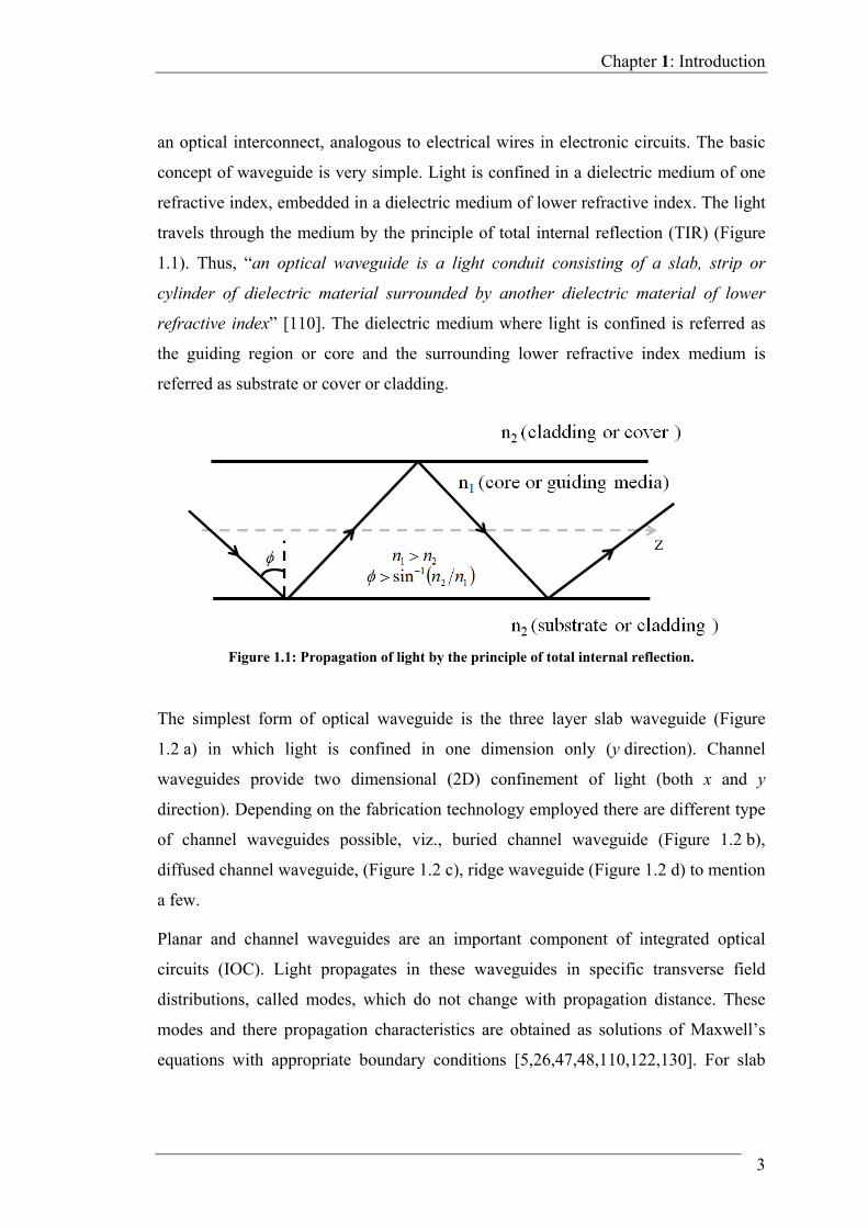
an optical interconnect, analogous to electrical wires in electronic circuits. The basic
concept of waveguide is very simple. Light is confined in a dielectric medium of one
refractive index, embedded in a dielectric medium of lower refractive index. The light
travels through the medium by the principle of total internal reflection (TIR) (Figure
1.1). Thus, “an optical waveguide is a light conduit consisting of a slab, strip or
cylinder of dielectric material surrounded by another dielectric material of lower
refractive index” [110]. The dielectric medium where light is confined is referred as
the guiding region or core and the surrounding lower refractive index medium is
referred as substrate or cover or cladding.
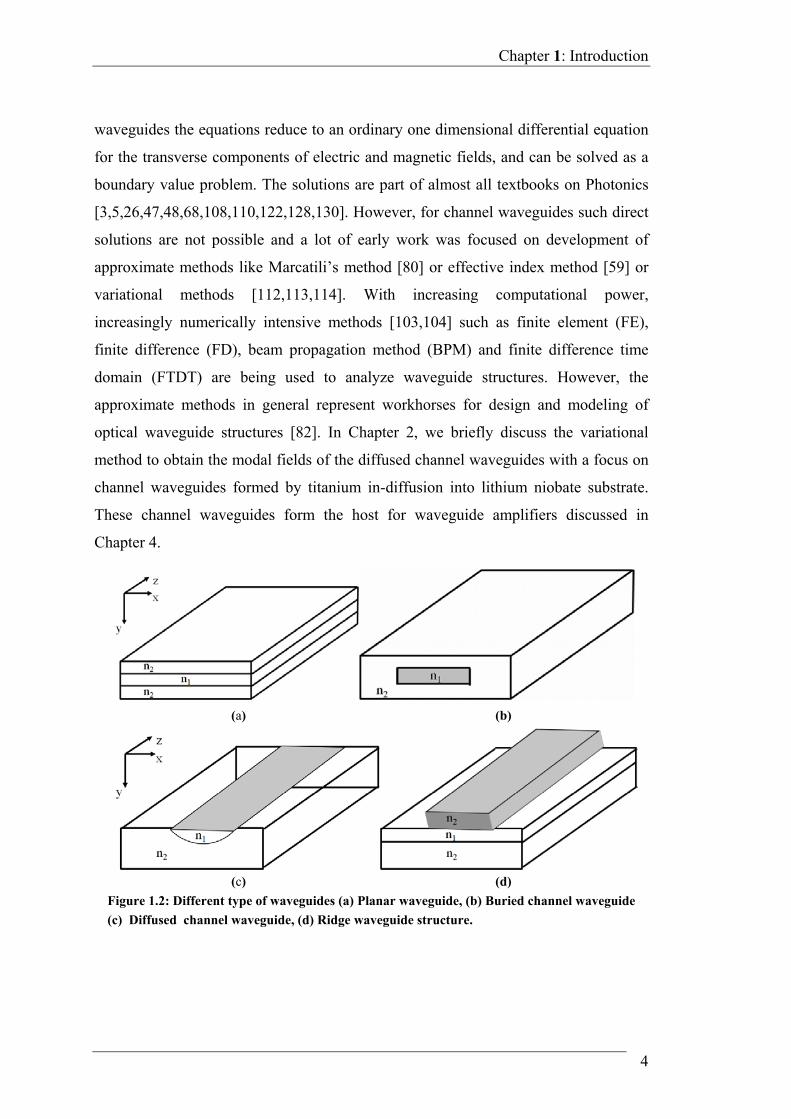
The simplest form of optical waveguide is the three layer slab waveguide (Figure
1.2 a) in which light is confined in one dimension only (y direction). Channel
waveguides provide two dimensional (2D) confinement of light (both x and y
direction). Depending on the fabrication technology employed there are different type
of channel waveguides possible, viz., buried channel waveguide (Figure 1.2 b),
diffused channel waveguide, (Figure 1.2 c), ridge waveguide (Figure 1.2 d) to mention
a few.
Planar and channel waveguides are an important component of integrated optical
circuits (IOC). Light propagates in these waveguides in specific transverse field
distributions, called modes, which do not change with propagation distance. These
modes and there propagation characteristics are obtained as solutions of Maxwell’s
equations with appropriate boundary conditions [5,26,47,48,110,122,130]. For slab
Figure 1.1: Propagation of light by the principle of total internal reflection.
Chapter 1: Introduction
4
waveguides the equations reduce to an ordinary one dimensional differential equation
for the transverse components of electric and magnetic fields, and can be solved as a
boundary value problem. The solutions are part of almost all textbooks on Photonics
[3,5,26,47,48,68,108,110,122,128,130]. However, for channel waveguides such direct
solutions are not possible and a lot of early work was focused on development of
approximate methods like Marcatili’s method [80] or effective index method [59] or
variational methods [112,113,114]. With increasing computational power,
increasingly numerically intensive methods [103,104] such as finite element (FE),
finite difference (FD), beam propagation method (BPM) and finite difference time
domain (FTDT) are being used to analyze waveguide structures. However, the
approximate methods in general represent workhorses for design and modeling of
optical waveguide structures [82]. In Chapter 2, we briefly discuss the variational
method to obtain the modal fields of the diffused channel waveguides with a focus on
channel waveguides formed by titanium in-diffusion into lithium niobate substrate.
These channel waveguides form the host for waveguide amplifiers discussed in
Chapter 4.
(a) (b)
(c) (d)
Figure 1.2: Different type of waveguides (a) Planar waveguide, (b) Buried channel waveguide
(c) Diffused channel waveguide, (d) Ridge waveguide structure.
Chapter 1: Introduction
5
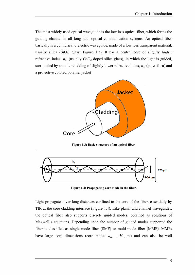
The most widely used optical waveguide is the low loss optical fiber, which forms the
guiding channel in all long haul optical communication systems. An optical fiber
basically is a cylindrical dielectric waveguide, made of a low loss transparent material,
usually silica (SiO2) glass (Figure 1.3). It has a central core of slightly higher
refractive index, n1, (usually GeO2 doped silica glass), in which the light is guided,
surrounded by an outer cladding of slightly lower refractive index, n2, (pure silica) and
a protective colored polymer jacket
.
Light propagates over long distances confined to the core of the fiber, essentially by
TIR at the core-cladding interface (Figure 1.4). Like planar and channel waveguides,
the optical fiber also supports discrete guided modes, obtained as solutions of
Maxwell’s equations. Depending upon the number of guided modes supported the
fiber is classified as single mode fiber (SMF) or multi-mode fiber (MMF). MMFs
have large core dimensions (core radius coa μm50~ ) and can also be well
Figure 1.3: Basic structure of an optical fiber.
Figure 1.4: Propagating core mode in the fiber.
Chapter 1: Introduction
6
understood by the simpler ray optics. SMFs on the other hand have core dimensions
close to wavelength, μm5~coa and hence, it is necessary to understand propagation
in them in terms of electromagnetic wave propagation based on Maxwell equations.
Since most waveguides are made of glass, the so called weakly guiding condition,
121 nnn is applicable and as a result a considerable simplification ensures in the
theoretical analysis. In particular, it is possible to find linearly polarized (LP) modes
of the structure which form useful approximations to the true hybrid modes [3,122]. In
an SMF, the cylindrical dielectric waveguide of radius, coa , formed by the core-
cladding interface supports only a single bound (LP01) mode confined to the core area
also referred to as the core mode or core guided mode. Most textbooks solve for these
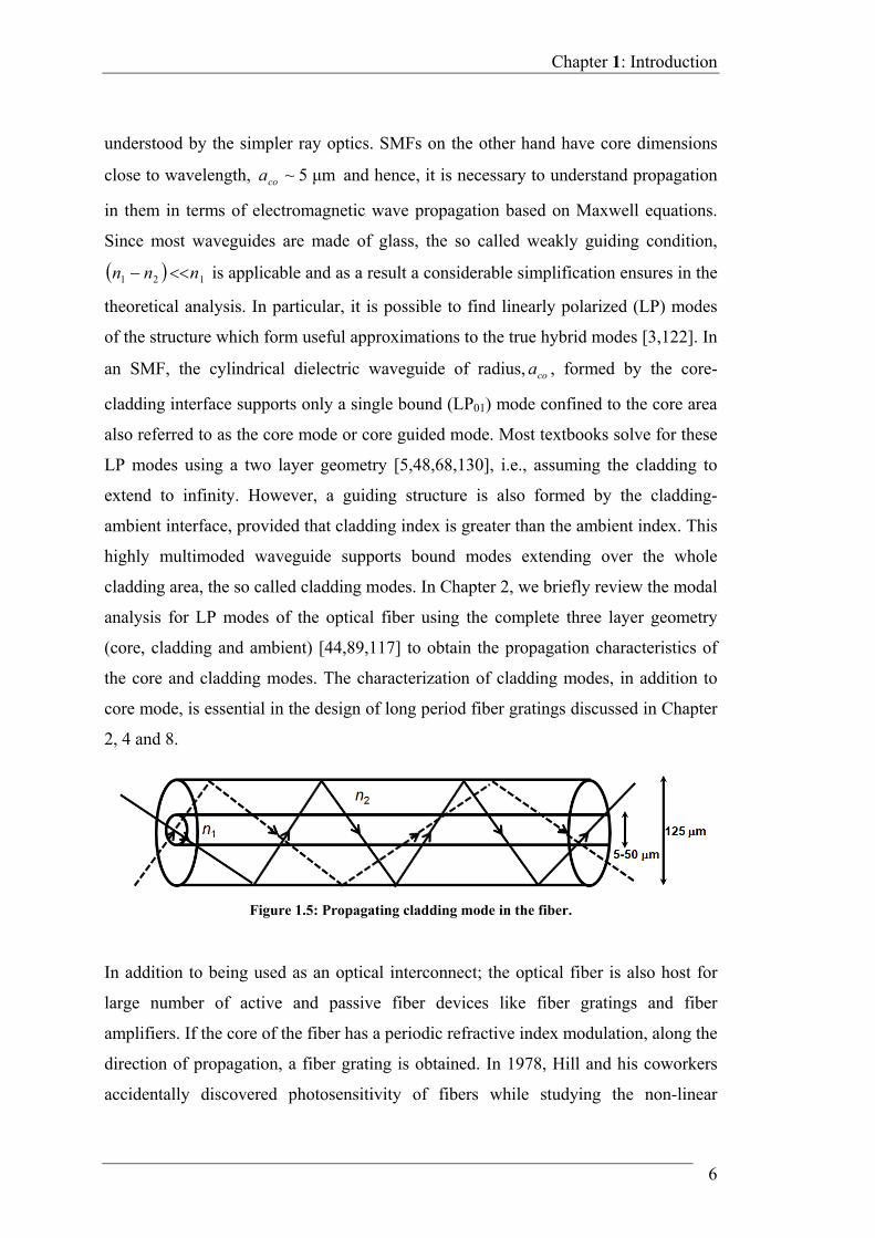
LP modes using a two layer geometry [5,48,68,130], i.e., assuming the cladding to
extend to infinity. However, a guiding structure is also formed by the cladding-
ambient interface, provided that cladding index is greater than the ambient index. This
highly multimoded waveguide supports bound modes extending over the whole
cladding area, the so called cladding modes. In Chapter 2, we briefly review the modal
analysis for LP modes of the optical fiber using the complete three layer geometry
(core, cladding and ambient) [44,89,117] to obtain the propagation characteristics of
the core and cladding modes. The characterization of cladding modes, in addition to
core mode, is essential in the design of long period fiber gratings discussed in Chapter
2, 4 and 8.
In addition to being used as an optical interconnect; the optical fiber is also host for
large number of active and passive fiber devices like fiber gratings and fiber
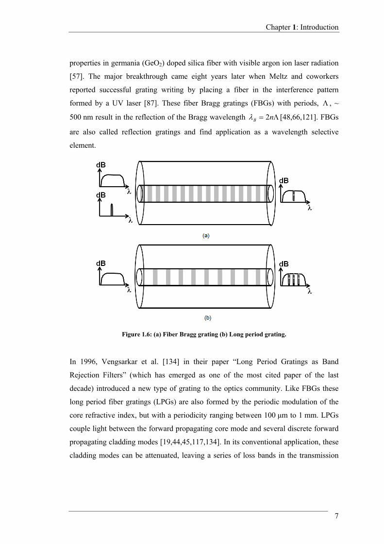
amplifiers. If the core of the fiber has a periodic refractive index modulation, along the
direction of propagation, a fiber grating is obtained. In 1978, Hill and his coworkers
accidentally discovered photosensitivity of fibers while studying the non-linear
Figure 1.5: Propagating cladding mode in the fiber.
Chapter 1: Introduction
7
properties in germania (GeO2) doped silica fiber with visible argon ion laser radiation
[57]. The major breakthrough came eight years later when Meltz and coworkers
reported successful grating writing by placing a fiber in the interference pattern
formed by a UV laser [87]. These fiber Bragg gratings (FBGs) with periods, , ~
500 nm result in the reflection of the Bragg wavelength nB 2 [48,66,121]. FBGs
are also called reflection gratings and find application as a wavelength selective
element.
In 1996, Vengsarkar et al. [134] in their paper “Long Period Gratings as Band
Rejection Filters” (which has emerged as one of the most cited paper of the last
decade) introduced a new type of grating to the optics community. Like FBGs these
long period fiber gratings (LPGs) are also formed by the periodic modulation of the
core refractive index, but with a periodicity ranging between 100 μm to 1 mm. LPGs
couple light between the forward propagating core mode and several discrete forward
propagating cladding modes [19,44,45,117,134]. In its conventional application, these
cladding modes can be attenuated, leaving a series of loss bands in the transmission
Figure 1.6: (a) Fiber Bragg grating (b) Long period grating.

Chapter 1: Introduction
8
spectrum (Figure 1.6). This property makes the LPG a band rejection filter and finds
application in gain flattening filters for optical amplifiers [51,107,143].
Emergence of erbium doped fiber amplifier (EDFA) in 1987 [35,83,84] was one of the
most important developments that revolutionized optical telecommunication. EDFA
mainly consists of a silica glass fiber (usually 4 m to 50 m long), in which the core is
doped with erbium ions. The erbium ions in a silica host when pumped by a 980 nm
pump radiation can amplify many wavelength channels within the C and L band, i.e.,
a wavelength range of 1.53-1.6 m. Thus, one can use a single amplifier for all
wavelengths in wavelength division multiplexed (WDM) or dense wavelength
division multiplexed (DWDM) systems. However, EDFA suffers from two
limitations: (i) that the gain is not same for all signal wavelengths, (ii) the presence of
amplified spontaneous emission (ASE) noise. One of the techniques for gain flattening
is the use of an external optical gain flattening filter (GFF) having a loss profile that is
reverse of the gain spectra of EDFA [51,107,143]. However, in these gain equalization
is achieved by attenuating the wavelengths with higher gain, hence reducing the
efficiency. Recently, Singh et al. [119] proposed that an appropriately chosen long
period grating written through a length of the erbium doped fiber (EDF) itself can
bring about gain flattening. As a result, in this configuration, there was gain flattening
as well as increase in the average gain across the 1.54-1.56 m band.
We expect that LPG written in EDF itself would also affect the amplification of
spontaneous emission, and hence, the noise characteristics of the amplifier. The
amplified spontaneous emission essentially contributes to noise and depletes the
population inversion. ASE in the same direction as the signal is a major source of
cumulative noise (reducing signal to noise ratio), while backward propagating ASEs
can harm source lasers if not isolated. The spontaneous emission generated in each
small section of fiber has a random phase. LPG is a phase sensitive device, and hence,
it is necessary to take into account both the amplitude and phase of the propagating
spontaneous emission. We have evolved a methodology to incorporate ASE taking
into consideration the random phase of spontaneous emission. Our results show that
LPG written in EDF itself, not only brings about gain flattening, but also suppresses
the ASE noise. Further, amplified spontaneous emission is also used as a broadband
Chapter 1: Introduction
9
source. If an EDF with the LPG written in it is used for such a source, our results
show that, the output power spectrum of the source over the 1.53-1.56 m band is also
flattened.
In order to study the LPG written in an EDF for gain flattening and noise suppression,
we had to develop an understanding of LPGs and its applications. In Chapter 2, we
briefly review the coupled mode theory to analyze the coupling of power between the
core mode and different cladding modes [121,122] of a LPG. A specific feature of
LPGs is the sensitivity of the transmission spectrum to the refractive index of
ambient ambn , i.e., the material surrounding the cladding of fiber [19,134], because the
effective indices of the cladding modes, mcleffn , , are strongly influenced by the ambient
refractive index. The primary effect of change in the ambient refractive index is the
consequent change in resonant wavelength. Hence, several authors have exploited this
feature of a LPG to implement refractive index sensors based on the change in
resonance wavelength, [18,96,115,134,146] i.e., they measure the small shift in the
resonance wavelength with change in ambient refractive index. The limitation of this
technique is that the measurement of such small wavelength shifts requires the use of
relatively expensive high-resolution optical spectrum analyzers (OSA). In Chapter 8,
we present an alternative approach for measurement of refractive index using a LPG.
In our method a LPG is interrogated by a single wavelength source and, instead of
measuring the shift in resonance, the change in the power retained in the core mode
due to change in ambient index is measured. We present a criterion to design the LPG
based refractive index sensor, which takes into account the desired refractive index
range and maximizes the sensitivity.
Analogous to the EDFA is the erbium doped waveguide amplifier (EDWA) that uses a
channel waveguide instead of a fiber to confine and amplify the optical signal.
LiNbO3 (lithium niobate) has been an attractive host material for the development of
active and passive integrated optical components and titanium in-diffused LiNbO3
waveguides form the backbone of integrated optical circuits (IOCs) in LiNbO3.
Doping LiNbO3 waveguides with erbium ions, under appropriate pumping conditions
forms an amplifying channel for wavelengths around 1.53 m. A rigorous modeling
of the EDWA implies numerical solution of coupled differential equations, which
Chapter 1: Introduction
10
require the computation of integrals containing modal intensity and erbium density
distribution across the doped area at each step. Hence, obtaining the gain
characteristics for even one signal wavelength is time consuming, and when ASE,
which is spread over the entire gain spectrum region, is considered the modeling is
computationally expensive. In Chapter 4, we have proposed approximations for the
modal fields, which reduce these integrals to analytical forms. This results in
computationally efficient solution, especially when a large number of wavelengths are
co-propagating and iterative solutions of the differential equations are needed for
estimating the ASE.
For the last few years, telecommunication institutes around the world have shown lot
of interest in semiconductor optical amplifiers (SOA). There is a valid reason for this
interest. Firstly, they are compatible with monolithic integration and hence, offer a
low cost option. Secondly, their gain bandwidth can be moved almost without limit
over a wide range of wavelengths by choice of material composition, e.g., in InGaAsP
the range is from 1.2 to 1.6 m. With photonics moving near to end user, SOAs are
being explored as inline amplifiers or power boosters in metropolitan networks, with a
tough competition between bulk-SOAs, quantum well (QW) SOAs and quantum dot
(QD) SOAs [30,31,91]. On the other hand, due to strong nonlinear behavior SOAs
appear to be a convenient tool for optical data processing [30,31,91].
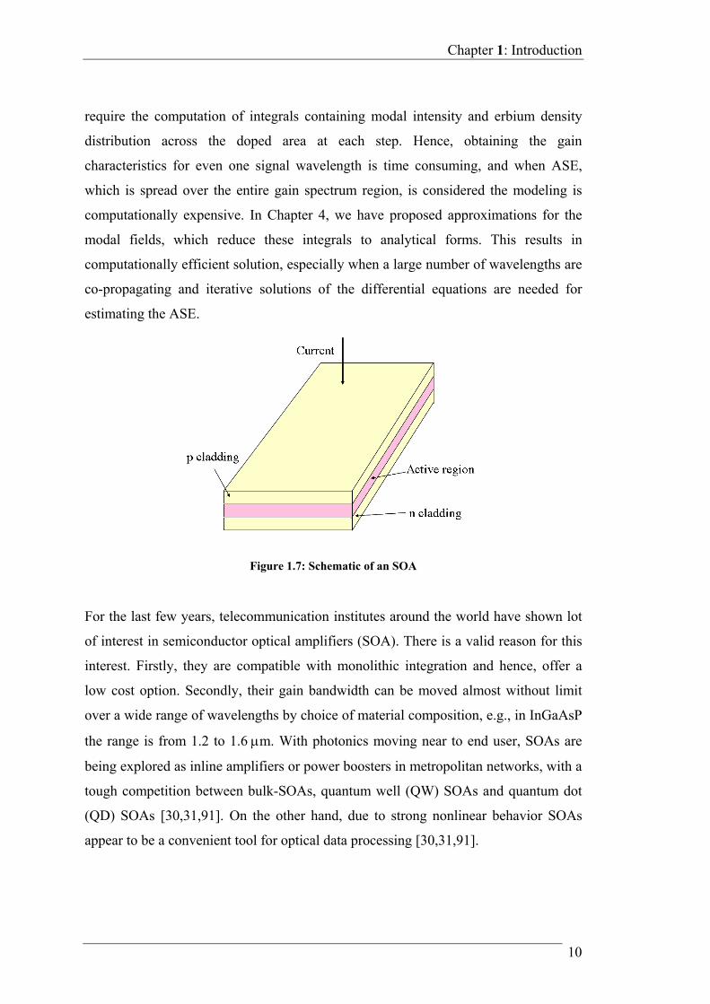
Figure 1.7: Schematic of an SOA
Chapter 1: Introduction
11
An SOA is essentially a semiconductor laser with no reflecting facets [147]. It has a
gain region (also called active layer) sandwiched between two cladding layers, one p-
doped and the other n-doped (Figure 1.7). Under proper biasing conditions, there
occurs a population inversion in the gain region, which is necessary for the
amplification of light. Several models have been developed in the past to simulate
SOAs [23,30,31,62,81], and depending on the behavior we want to simulate, one
model can be better than others. In general, they all solve rate equations, i.e., time
dependent differential equations for the carrier and photon densities, and either,
average the carrier density over the entire length of the device or segment the SOA
into small segments. While the rate equations provide a fast means to predict the
behavior of an SOA, for better understanding and designing one needs a tool which
takes into account all the physics of the semiconductor. (Some of the basic
semiconductor physics relevant to the understanding of an SOA and its modeling is
given in Chapter 5). We need a tool, which calculates the basic material parameters
and their dependence on applied electric and optical fields. Silvaco’s ATLAS is one
such physics based tool. However, ATLAS supports only Lasers, LEDs,
photodetectors and Solar cells among the optical devices. We have developed a
methodology to extend the capability of ATLAs for modeling of SOAs as described in
Chapter 6.
As mentioned above, ATLAS is a versatile simulation tool with the capability to
include various physical effects important for semiconductor lasers. An SOA is
essentially a semiconductor laser with low mirror reflectivities [30,31,42,91]. Thus,
theoretically speaking by reducing the mirror reflectivities in the ATLAS LASER
module, we should be able to model an SOA. This can provide us with the
information regarding gain and ASE spectrum of the SOA under no signal conditions.
However, this information is insufficient. An SOA as an amplifier or optical signal
processor operates on an input optical signal. For complete characterization of an
SOA it is important to know how the gain and carrier densities of the amplifier change
(gain saturation and gain recovery) in response to the optical signal. Unfortunately,
ATLAS has no support for an optical input to an SOA. Hence, we had to improvise,
from the existing models in ATLAS, a way that will have the similar effect on carriers
Chapter 1: Introduction
12
and gain as an input optical signal has. We developed a technique of implementing a
virtual optical source in ATLAS and characterized two experimentally well defined
SOAs. Our results show a good match with the experimental data, thus, proving that
we can extend the capabilities of ATLAS to engineer SOAs.
Having established this extended capability, we further investigated the effect of
various modifications in SOA design to improve device performance. Specifically, we
considered the modifications in doping, active layer depth and ridge width. Our results
show that these changes in the SOA design have a significant effect on the SOA
saturation and recovery behavior. A p-doped SOA on proper bias (high injection
current) can be more suitable for amplifying applications, and an n-doped SOA more
suitable for signal processing applications. Further, smaller ridge width reduces
effective carrier lifetime, saturation powers, and at same time increases the alpha
factor and is hence better suited for optical signal processing applications. Decrease in
the depth of active region, decreases the confinement factor, and reduces effective
carrier lifetime. This results in increase of both input and output saturation powers,
making an SOA with small active layer depths would be a better choice for in-line
optical amplification. The results of SOA engineering are presented in Chapter 7.
1.1 Achievements of the present work
The scope of this thesis is modeling, design and application of optical amplifiers and
long period gratings (LPGs). Typically, we concentrate on erbium doped fiber
amplifiers, erbium doped lithium niobate waveguide optical amplifiers (EDWAs), and
semiconductor optical amplifiers (SOAs). These three devices, besides being
employed as optical amplifiers, also promise their feasibility to be used as optical
signal processors. Modeling and simulation of these amplifiers is thus an important
tool in the understanding and designing of these amplifiers. This can further aid in the
development on structural modifications which can help in implementing new
technologies and look for novel applications of the same structure. In summary in the
present thesis we have achieved the following:
Evolved a methodology to work with complex amplitude coupled differential
equations instead of conventional power coupled equations for use in the study
Chapter 1: Introduction
13
of ASE in erbium doped fiber amplifiers. This was made possible by
developing a recipe to incorporate both, the amplitude and the random phase
of the spontaneous emission generated along the propagation length of the
EDF. The method was needed to analyze the possible ASE noise suppression
in EDF with the LPG written in it, a novel structure proposed by Singh
et al. [119] for gain flattened EDFs. We established the validity of our method
by comparing the results with well established power propagation equations
for EDF in the absence of LPG. Our results show that the novel structure not
only brings about gain flattening, but also suppresses the ASE noise.
Proposed field approximations for simplified gain and ASE calculations in
EDWA. Field approximations obtained by the variational analysis, for
titanium indiffused lithium niobate channel waveguides, by various authors
[3,60,61,112,113,114] were studied. These were further approximated to
reduce the integrals involved in gain and ASE noise characterization to
analytical forms. The reduction to analytical forms reduces the computation
time significantly for gain calculations when a large number of signals are
multiplexed and for ASE noise evaluation.
Developed a technique for implementing a virtual optical source in ATLAS and
characterized two experimentally well defined SOAs. ATLAS was chosen
because of its capability to accurately predict the electrical and optical
characteristics associated with specified bias conditions. Though the ATLAS
LASER module supports the simulation of semiconductor lasers, it cannot
provide optical input necessary for simulating SOAs. We modeled a virtual
optical source by manually changing the radiative recombination parameter to
simulate the decrease of carrier concentration that would physically result
from an external optical signal. Our results showed a good match with
available experimental data, thus, proving that we can extend the capabilities
of ATLAS in modeling SOA.
Used the extended capability of ATLAS in SOA engineering. We investigated
the effect of various modifications in SOA design to improve device
performance. We considered the modifications in doping, active layer depth
and ridge width. Our results show that these changes in the SOA design have a
Chapter 1: Introduction
14
significant effect on the SOA saturation and recovery behavior. A p-doped
SOA on proper bias (high injection current) can be more suitable for
amplifying applications, and an n-doped SOA more suitable for signal
processing applications. Smaller ridge width reduces effective carrier lifetime,
saturation powers, and at same time increase alpha factor. Decrease in the
depth of active region, decreases the confinement factor, and reduces effective
carrier lifetime. Thus depending upon the SOA application we can engineer
the SOA design.
Developed a criterion to design a long period grating for refractive index
sensing around desired ambient index when only one interrogating wavelength
is to be used. The design is based on power measurement and maximizes the
sensitivity around the desired refractive index range.
The above work has resulted in the following publications:
1. G. Jain, Amita Kapoor and E. K. Sharma, Er-LiNbO3 Waveguide: field
approximation for simplified gain calculations in DWDM applications, J. Opt.
Soc. America B, 26(4), 633-639, (2009).
2. Amita Kapoor and E. K. Sharma, Long Period Grating Refractive Index
Sensor: Optimal Design For Single Wavelength Interrogation, Appl. Opt. 48,
G88-G94, (2009).
3. R. Singh, Amita Kapoor and E. K. Sharma, Long Period Gratings in erbium
Doped Fibers: Gain Flattening and ASE Reduction, Photonics 2004 (Seventh
International conference on Optoelectronics, Fiber optics and Photonics),
Cochin, India, 9-11th December (2004).
4. G. Jain, Amita Kapoor, and E. K. Sharma, Simplified Modeling of titanium
indiffused LiNbO3 Waveguide Amplifiers, Photonics 2006 (Eighth International
Conference on Optoelectronics, Fiber-optics and Photonics), University of
Hyderabad, Hyderabad, India, 12-16th December (2006).
5. Amita Kapoor, G. Jain and E. K. Sharma, Simplified Gain Calculations in
erbium doped LiNbO3 waveguides. Proc. SPIE 6468, 646808, (2007).

Chapter 1: Introduction
15
6. Amita Kapoor, R. Singh and E. K. Sharma, Suppression of Amplified
Spontaneous Emission in erbium Doped Fiber with Long Period Grating
written in it, Microwave Conference, 2007. APMC 2007. Asia-Pacific, 1-4,
(2007).
7. Amita Kapoor, R. Singh and E. K. Sharma, Estimation of Amplified
Spontaneous Emission in erbium Doped Fiber with Long Period Grating
Written in it, The Second Research Forum of Japan-Indo Collaboration Project
on Infrastructural Communication Technologies Supporting Fully Ubiquitous
Information Society, Kyushu University, Fukuoka, Japan, Forum Digest, 57-
61, (2007).
8. Amita Kapoor, G. Jain and E. K. Sharma, Er-LiNbO3 Waveguide: Simplified
Gain Calculations for DWDM Application, 2007 Japan-Indo Workshop on
Microwaves, Photonics and Communication Systems, Kyushu University,
Fukuoka, Japan. Workshop Digest, 113-118, (2007).
9. Amita Kapoor and E. K. Sharma, Long Period Grating Refractive Index
Sensor: Optimal Design For Single Wavelength Interrogation, 2008 Japan-
Indo Workshop on Microwaves, Photonics and Communication Systems,
Kyushu University, Fukuoka, Japan. Workshop Digest, (2008).
10. G. Jain, Amita Kapoor and E. K. Sharma, Er-LiNbO3 Waveguide: Field
Approximations for Simplified Gain Calculations in DWDM Application,
Photonics 2008 (Ninth International Conference on Optoelectronics, Fiber-
optics and Photonics), Delhi, India, 13-17th December (2008).
11. Amita Kapoor and E. K. Sharma; Long Period Grating Refractive Index
Sensor: Optimal Design For Single Wavelength Interrogation, Photonics 2008
(Ninth International Conference on Optoelectronics, Fiber-optics and
Photonics), Delhi, India, 13-17th December (2008).
12. Amita Kapoor, E. K. Sharma, W. Freude and J. Leuthold, Saturation
Characteristics of InGaAsP-InP bulk SOA, Proc. SPIE 7597, 75971I (2010).
13. W. Freude, R. Bonk, T. Vallaitis, A. Marculescu, Amita Kapoor, C. Meuer,
D. Bimberg, R. Brenot, F. Lelarge, G. H. Duan and J. Leuthold Semiconductor

Chapter 1: Introduction
16
optical amplifiers (SOA) for linear and nonlinear applications, Deutsche
Physikalische Gesellschaft e.V., Regensberg , 21-26th March 2010.
14. W. Freude, R. Bonk, T. Vallaitis, A. Marculescu, Amita Kapoor, E. K.
Sharma, C. Meuer, D. Bimberg, R. Brenot, F. Lelarge, G. H. Duan, C. Koos
and J. Leuthold, Linear and nonlinear semiconductor optical amplifiers, 2010
12th International Conference on Transparent Optical Networks (ICTON), 1-4,
(2010).
Chapter 2: Waveguidance, mode coupling in fiber gratings and optical amplifiers: Theoretical background
17
2 Waveguidance, mode coupling in fiber gratings and optical amplifiers: Theoretical background
2.1 Introduction
Waveguides are an essential component of all optical communication systems. In
addition to being the physical channel for guided optical communication systems in
the form of optical fibers (optical interconnect) they also form the host for active and
passive optical devices. Wave propagation through these waveguides in well defined
electromagnetic modes is studied by Maxwell’s equations using the appropriate
boundary conditions.
In this chapter, for completeness, we first review the basic Maxwell’s equations
governing the propagation of the electromagnetic modes in optical waveguides. We
then outline the procedure for obtaining the propagation characteristics of the modes
propagating in the single mode diffused channel waveguides using the variational
analysis. Specifically we look into the channel waveguides formed by the in-diffusion
of titanium into lithium niobate to obtain an analytical description of the modal fields
of the diffused channel waveguide and these results are later used in Chapter 4 to

Chapter 2: Waveguidance, mode coupling in fiber gratings and optical amplifiers: Theoretical background
18
obtain simplified analytical expressions for the gain and noise characteristics of the
erbium doped waveguide amplifier (EDWA).
After channel waveguides, we move onto the most widely used optical waveguide: the
optical fiber. We briefly review the modal analysis of the optical fiber in the weakly
guiding approximation using all the three layers, i.e., core cladding and ambient to
obtain the propagation characteristics of the linearly polarized (LP) core guided and
cladding guided modes of the optical fiber. These results are used to understand the
mode coupling in long period fiber gratings. Application of long period gratings
written in erbium doped fibers for gain flattening and noise suppression is discussed in
Chapter 3.
Finally, we review the underlying physics behind the process of optical amplification.
The main focus of this thesis is on optical amplifiers, hence this discussion forms the
foundation.
2.2 Maxwell’s equations
In a charge free, non-magnetic dielectric medium the electric field vector ),,,( tzyxE
,
the magnetic field vector ),,,( tzyxH
, the electric flux density ),,,( tzyxD
and the
magnetic flux density ),,,( tzyxB
are related by Maxwell’s equations:
0 D
(2.1)
0 B
(2.2)
t
HE
0 (2.3)
t
DH
(2.4)
with ED
and HB
0 , where r 0 is the dielectric permittivity of the
material. 0 is the permittivity of free space, zyxr ,, is the relative permittivity,
and 0 is the magnetic permeability of the non magnetic medium. For an isotropic
medium the dielectric permittivity zyx ,, is a scalar and the relative permittivity is
Chapter 2: Waveguidance, mode coupling in fiber gratings and optical amplifiers: Theoretical background
19
related to the refractive index, n(x,y,z), by relation, 2nr . However, in any general
anisotropic medium, in the principal coordinate system of the crystal, zyx ,, is a
diagonal tensor given by:
r
r
r
3
2
1
0
00
00
00
(2.5)
and the electric flux density ),,,( tzyxD
can be written as:
z
y
x
r
r
r
z
y
x
E
E
E
D
D
D
3
2
1
0
00
00
00
(2.6)
In a uniaxial medium, like lithium niobate, 221 orr n , and 2
3 exr n , where on is
the ordinary refractive index, exn is the extra ordinary refractive index and the crystal
z-axis is the optic axis. Waveguidance in dielectric waveguides is made possible due
to the difference in refractive index of core (guiding medium) and the cladding
(substrate or cover). Most practical waveguides are weakly guiding, i.e., the refractive
index of cladding (substrate) is not very different from that of core. In general for an
inhomogeneous medium, using the Maxwell’s equation one can easily derive the wave
equation describing the propagation of an electromagnetic wave:
2
2
02
22 1
t
DEn
nE
(2.7)
For an infinitely homogenous medium, the second term on the LHS is zero
everywhere and each Cartesian component, (Ex, Ey or Ez.), obeys the scalar wave
equation:
2
2
2
22
tc
n
(2.8)
where tzyx ,,, may represent Ex, Ey or Ez and 00/1 c is the speed of light in
free space. The solutions of above equation are in the form of uniform plane waves
with only transverse electric and magnetic components. It should be noted that in an
anisotropic medium different polarizations see a different refractive indices, e.g. in
Chapter 2: Waveguidance, mode coupling in fiber gratings and optical amplifiers: Theoretical background
20
lithium niobate, the x or y polarized waves propagating along the z-direction see the
ordinary refractive index on , while a z-polarized wave propagating along the x or y
direction will see the extra ordinary index, exn .
For medium with gradually varying dielectric properties, i.e., when the refractive
index varies sufficiently slowly so that it can be assumed constant within distances of
the order of wavelength, the second term on the LHS of Eq. (2.7) is negligible in
comparison. For such a medium with weak homogeneity the electromagnetic waves
are nearly transverse in nature with transverse component of the electric field
satisfying the scalar wave equation (2.8). In a typical waveguide with propagation
along z-direction, the refractive index is independent of z and varies only with the
transverse coordinates, i.e.,: yxnzyxn ,,, 22 , and assuming time harmonic fields
the solution for the transverse component can be written as:
ztieyxtzyx ,,,, (2.9)
where is the propagation constant, 0kneff is called the effective index, where
00 2 k , 0 being the free space wavelength, yx, determines the transverse
field distribution (also called modal field) of the guided mode and satisfies the
following differential equation, also known as Helmholtz equation, with appropriate
boundary conditions:
0),(),( 2220
2 yxnnkyx efft (2.10)
with 22
2
yxt
. The solution of this Helmholtz equation defines the modal
fields in a guided structure. The Eq. (2.10) is in fact an eigenvalue equation with
yx, being the eigenfunction and 2effn or 2 being the eigenvalue of the operator
20
2 kt . Only certain discrete solutions, known as the guided modes and a continuum
of solutions referred as radiation modes are allowed. A mode represents a field
configuration which propagates along the waveguide without any change in
polarization or in the field distribution except for change in phase. Guided modes are
confined within the guiding medium, while radiation modes are not bound to the
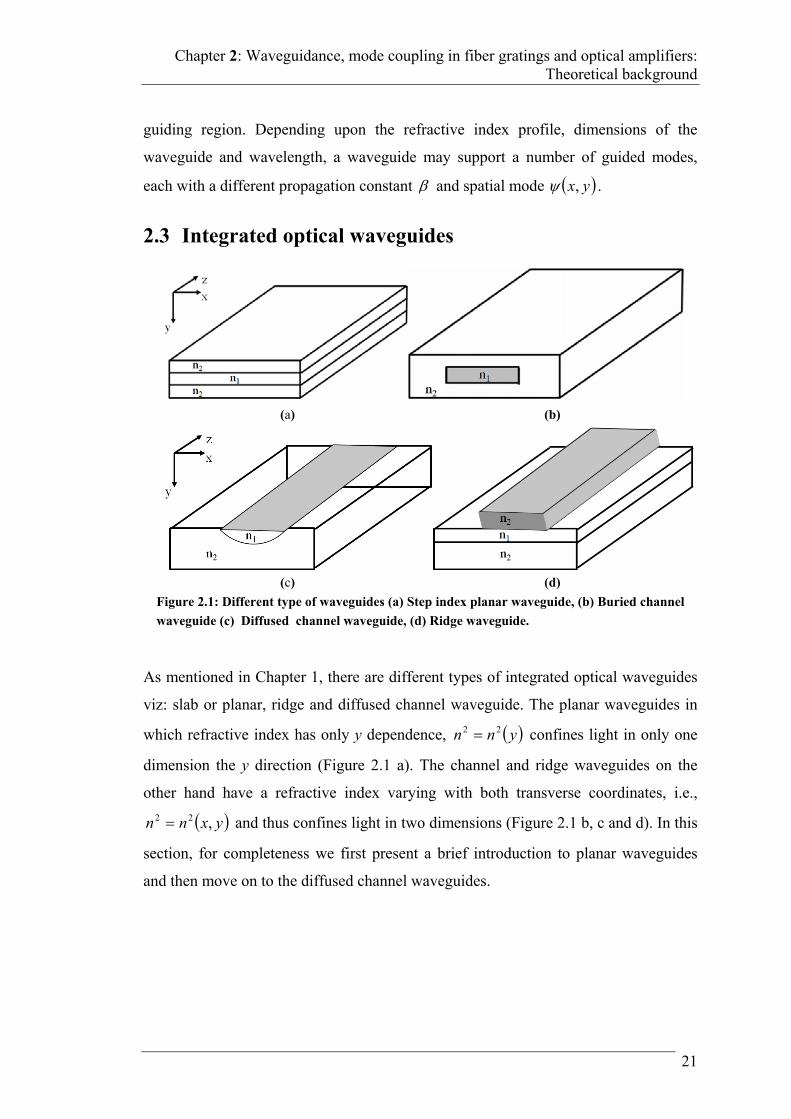
Chapter 2: Waveguidance, mode coupling in fiber gratings and optical amplifiers: Theoretical background
21
guiding region. Depending upon the refractive index profile, dimensions of the
waveguide and wavelength, a waveguide may support a number of guided modes,
each with a different propagation constant and spatial mode yx, .
2.3 Integrated optical waveguides
As mentioned in Chapter 1, there are different types of integrated optical waveguides
viz: slab or planar, ridge and diffused channel waveguide. The planar waveguides in
which refractive index has only y dependence, ynn 22 confines light in only one
dimension the y direction (Figure 2.1 a). The channel and ridge waveguides on the
other hand have a refractive index varying with both transverse coordinates, i.e.,
yxnn ,22 and thus confines light in two dimensions (Figure 2.1 b, c and d). In this
section, for completeness we first present a brief introduction to planar waveguides
and then move on to the diffused channel waveguides.
(a) (b)
(c) (d)
Figure 2.1: Different type of waveguides (a) Step index planar waveguide, (b) Buried channel
waveguide (c) Diffused channel waveguide, (d) Ridge waveguide.
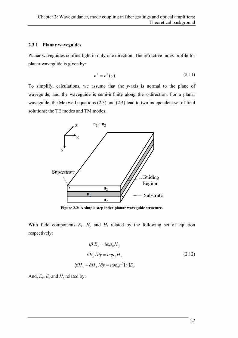
Chapter 2: Waveguidance, mode coupling in fiber gratings and optical amplifiers: Theoretical background
22
2.3.1 Planar waveguides
Planar waveguides confine light in only one direction. The refractive index profile for
planar waveguide is given by:
)(22 ynn (2.11)
To simplify, calculations, we assume that the y-axis is normal to the plane of
waveguide, and the waveguide is semi-infinite along the x-direction. For a planar
waveguide, the Maxwell equations (2.3) and (2.4) lead to two independent set of field
solutions: the TE modes and TM modes.
With field components Ex, Hy and Hz related by the following set of equation
respectively:
yx HiEi 0
zx HiyE 0/
xzy EyniyHHi 20/
(2.12)
And, Ey, Ez and Hx related by:
Figure 2.2: A simple step index planar waveguide structure.
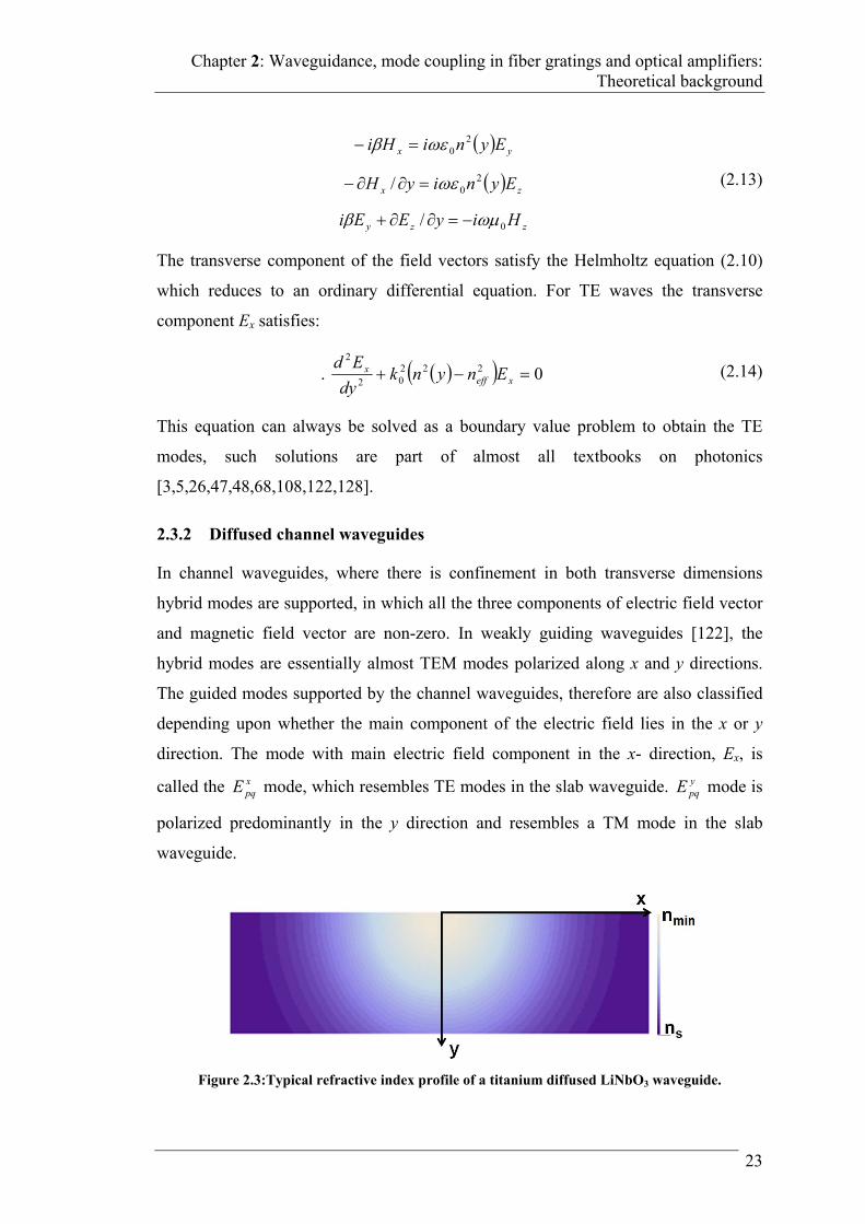
Chapter 2: Waveguidance, mode coupling in fiber gratings and optical amplifiers: Theoretical background
23
yx EyniHi 20
zx EyniyH 20/
zzy HiyEEi 0/
(2.13)
The transverse component of the field vectors satisfy the Helmholtz equation (2.10)
which reduces to an ordinary differential equation. For TE waves the transverse
component Ex satisfies:
. 022202
2
xeffx Enynk
dy
Ed (2.14)
This equation can always be solved as a boundary value problem to obtain the TE
modes, such solutions are part of almost all textbooks on photonics
[3,5,26,47,48,68,108,122,128].
2.3.2 Diffused channel waveguides
In channel waveguides, where there is confinement in both transverse dimensions
hybrid modes are supported, in which all the three components of electric field vector
and magnetic field vector are non-zero. In weakly guiding waveguides [122], the
hybrid modes are essentially almost TEM modes polarized along x and y directions.
The guided modes supported by the channel waveguides, therefore are also classified
depending upon whether the main component of the electric field lies in the x or y
direction. The mode with main electric field component in the x- direction, Ex, is
called the xpqE mode, which resembles TE modes in the slab waveguide. y
pqE mode is
polarized predominantly in the y direction and resembles a TM mode in the slab
waveguide.
Figure 2.3:Typical refractive index profile of a titanium diffused LiNbO3 waveguide.
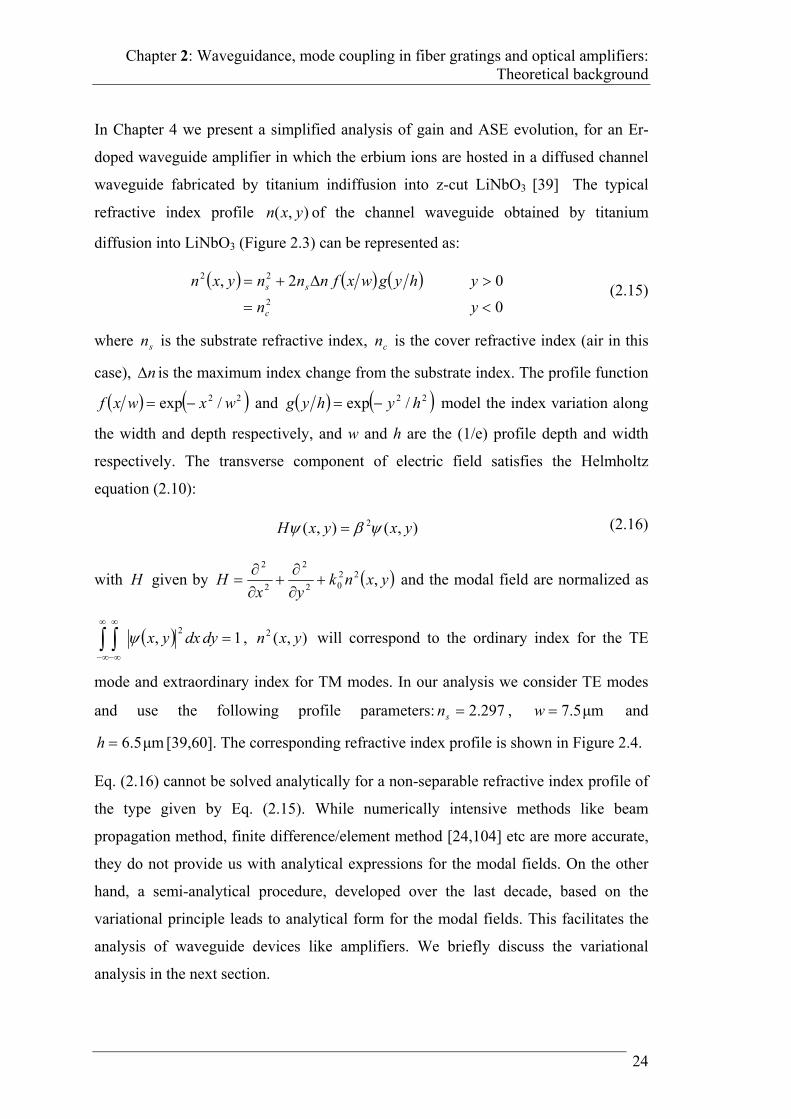
Chapter 2: Waveguidance, mode coupling in fiber gratings and optical amplifiers: Theoretical background
24
In Chapter 4 we present a simplified analysis of gain and ASE evolution, for an Er-
doped waveguide amplifier in which the erbium ions are hosted in a diffused channel
waveguide fabricated by titanium indiffusion into z-cut LiNbO3 [39] The typical
refractive index profile ),( yxn of the channel waveguide obtained by titanium
diffusion into LiNbO3 (Figure 2.3) can be represented as:
0
02,2
22
yn
yhygwxfnnnyxn
c
ss (2.15)
where sn is the substrate refractive index, cn is the cover refractive index (air in this
case), n is the maximum index change from the substrate index. The profile function
22 /exp wxwxf and 22 /exp hyhyg model the index variation along
the width and depth respectively, and w and h are the (1/e) profile depth and width
respectively. The transverse component of electric field satisfies the Helmholtz
equation (2.10):
),(),( 2 yxyxH (2.16)
with H given by yxnkyx
H ,2202
2
2
2
and the modal field are normalized as
1,2
dydxyx , ),(2 yxn will correspond to the ordinary index for the TE
mode and extraordinary index for TM modes. In our analysis we consider TE modes
and use the following profile parameters: 297.2sn , μm5.7w and
μm5.6h [39,60]. The corresponding refractive index profile is shown in Figure 2.4.
Eq. (2.16) cannot be solved analytically for a non-separable refractive index profile of
the type given by Eq. (2.15). While numerically intensive methods like beam
propagation method, finite difference/element method [24,104] etc are more accurate,
they do not provide us with analytical expressions for the modal fields. On the other
hand, a semi-analytical procedure, developed over the last decade, based on the
variational principle leads to analytical form for the modal fields. This facilitates the
analysis of waveguide devices like amplifiers. We briefly discuss the variational
analysis in the next section.
Chapter 2: Waveguidance, mode coupling in fiber gratings and optical amplifiers: Theoretical background
25
2.3.2.1 Variational principle
From Eq. (2.16), multiplying by ),(* yx on both sides and integrating over the entire
cross section of waveguide, a stationary expression for the effective index is obtained:
dydxyxyxndydxyxyxk
n teff
222*20
2 ,,,,1
(2.17)
An approximation is chosen for the modal field ),....,;,( 21 nt aaayx , generally
known as the trial field, with naaa ,...., 21 as n adjustable variational parameters. This
trial field is substituted in the RHS of Eq. (2.17), which is then maximized with
respect to the variational parameters. The maximum value gives an estimate of the
effective index of the lowest mode and the corresponding ),....,;,( 21 nt aaayx with
the corresponding parameters an approximation for the modal field. Accuracy of the
variational method depends on the closeness of the assumed trial field to the exact
modal field of the guiding structure. It has been shown by earlier authors that one can
assume a separable variational trial field [60,61,129,112,113,114] and the following
three parameter variational field, with a Gaussian variation along the width and an
evanescent Hermite-Gaussian variation along the depth gives satisfactory results for
channel waveguides:
yYxXyxt , (2.18)
with
(a) (b)
Figure 2.4: Refractive index profile along (a) x-direction at y=0 and (b) y-direction at x=0 for
the channel waveguide with ns=2.297, n=0.0048, w=7.5 m, and h=6.5 m.
Chapter 2: Waveguidance, mode coupling in fiber gratings and optical amplifiers: Theoretical background
26
2
22
1exp1
w
xa
wdxX
x
(2.19)
and
0exp1
0exp11
2
2
2232
yh
ya
hd
yh
ya
h
ya
hdyY
y
y (2.20)
where 211 ad x , and 282222
133
22
1232
13
12 aaaaaad y ,
and 1a , 2a and 3a are the three variational parameter. Substituting the trial field in
the stationary expression of Eq. (2.17), closed form expression for the normalized
effective index is obtained:
yxs
seff
dd
sr
nn
nnb
2
22
(2.21)
with r and s as:
yxrrr and yx
x
xy
y
x dsV
dsVa
pds
222
11
2 (2.22)
with 21 asx , and 3322
32
2 84432 aaaaas y , nnwkV sx 20 ,
nnhkV sy 20 , nnnnp scs 222 , 2121 arx and ,
2
323
21232
22
23 214214212 aaaaary .
The three variational parameters are obtained by maximizing the expression for b. For
the channel waveguide in discussion at =1.532 m the three Variational parameters
obtained by maximizing b are a1 = 1.188, a2 = 47.46, and a3 = 1.099. And the
corresponding effective index value is 2.29807.
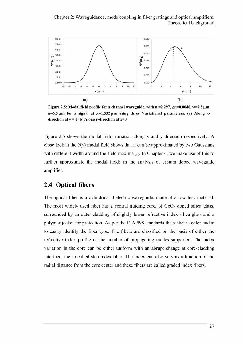
Chapter 2: Waveguidance, mode coupling in fiber gratings and optical amplifiers: Theoretical background
27
Figure 2.5 shows the modal field variation along x and y direction respectively. A
close look at the Y(y) modal field shows that it can be approximated by two Gaussians
with different width around the field maxima y0. In Chapter 4, we make use of this to
further approximate the modal fields in the analysis of erbium doped waveguide
amplifier.
2.4 Optical fibers
The optical fiber is a cylindrical dielectric waveguide, made of a low loss material.
The most widely used fiber has a central guiding core, of GeO2 doped silica glass,
surrounded by an outer cladding of slightly lower refractive index silica glass and a
polymer jacket for protection. As per the EIA 598 standards the jacket is color coded
to easily identify the fiber type. The fibers are classified on the basis of either the
refractive index profile or the number of propagating modes supported. The index
variation in the core can be either uniform with an abrupt change at core-cladding
interface, the so called step index fiber. The index can also vary as a function of the
radial distance from the core center and these fibers are called graded index fibers.
(a) (b)
Figure 2.5: Modal field profile for a channel waveguide, with ns=2.297, n=0.0048, w=7.5 m,
h=6.5 m for a signal at =1.532 m using three Variational parameters. (a) Along x-
direction at y = 0 (b) Along y-direction at x=0
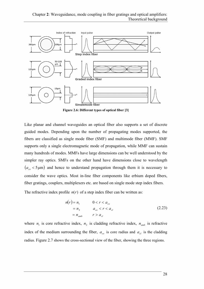
Chapter 2: Waveguidance, mode coupling in fiber gratings and optical amplifiers: Theoretical background
28
Like planar and channel waveguides an optical fiber also supports a set of discrete
guided modes. Depending upon the number of propagating modes supported, the
fibers are classified as single mode fiber (SMF) and multimode fiber (MMF). SMF
supports only a single electromagnetic mode of propagation, while MMF can sustain
many hundreds of modes. MMFs have large dimensions can be well understood by the
simpler ray optics. SMFs on the other hand have dimensions close to wavelength
μm5coa and hence to understand propagation through them it is necessary to
consider the wave optics. Most in-line fiber components like erbium doped fibers,
fiber gratings, couplers, multiplexers etc. are based on single mode step index fibers.
The refractive index profile )(rn of a step index fiber can be written as:
clamb
clco
co
arn
aran
arnrn
2
1 0
(2.23)
where 1n is core refractive index, 2n is cladding refractive index, ambn is refractive
index of the medium surrounding the fiber, coa is core radius and cla is the cladding
radius. Figure 2.7 shows the cross-sectional view of the fiber, showing the three regions.
Figure 2.6: Different types of optical fiber [3]
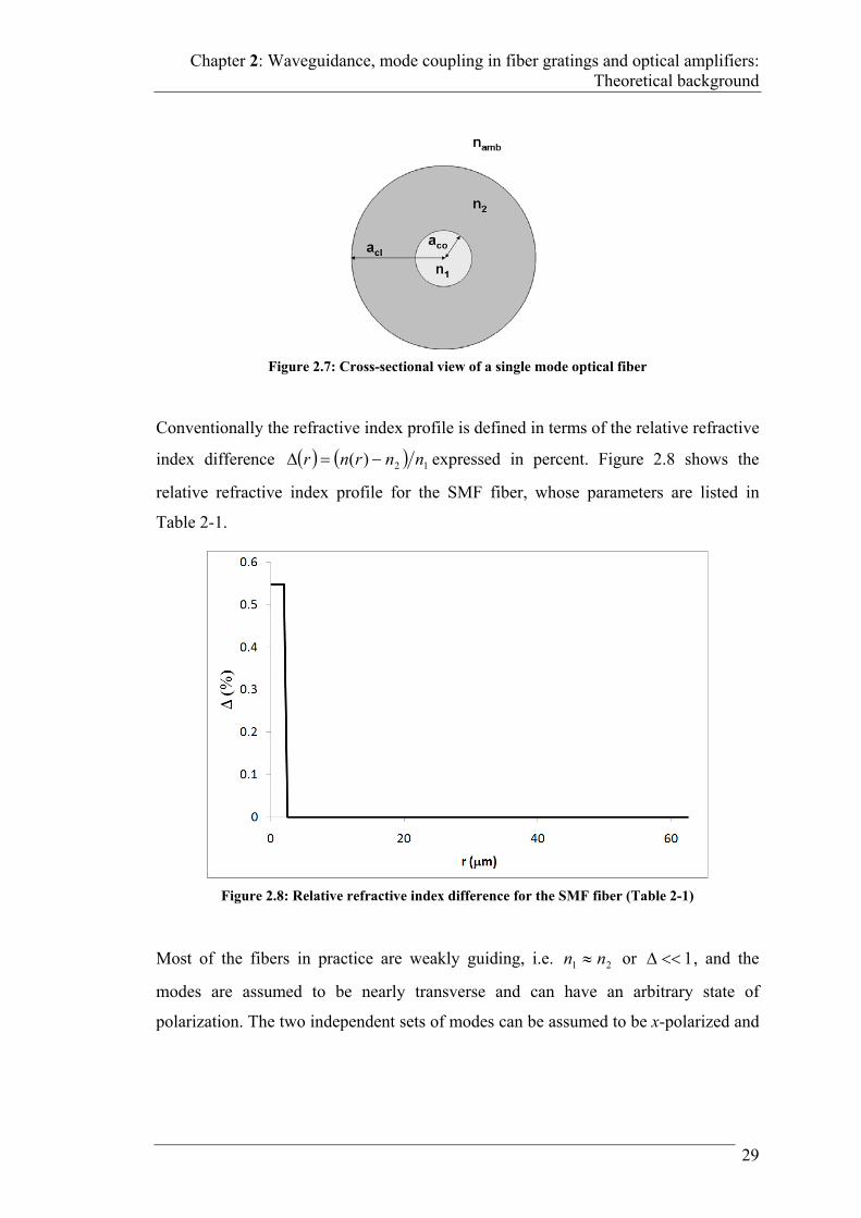
Chapter 2: Waveguidance, mode coupling in fiber gratings and optical amplifiers: Theoretical background
29
Conventionally the refractive index profile is defined in terms of the relative refractive
index difference 12)( nnrnr expressed in percent. Figure 2.8 shows the
relative refractive index profile for the SMF fiber, whose parameters are listed in
Table 2-1.
Most of the fibers in practice are weakly guiding, i.e. 21 nn or 1 , and the
modes are assumed to be nearly transverse and can have an arbitrary state of
polarization. The two independent sets of modes can be assumed to be x-polarized and
Figure 2.7: Cross-sectional view of a single mode optical fiber
Figure 2.8: Relative refractive index difference for the SMF fiber (Table 2-1)
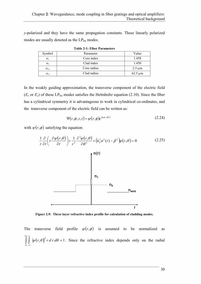
Chapter 2: Waveguidance, mode coupling in fiber gratings and optical amplifiers: Theoretical background
30
y-polarized and they have the same propagation constants. These linearly polarized
modes are usually denoted as the LPlm modes.
Table 2-1: Fiber Parameters
Symbol Parameter Value
n1 Core index 1.458
n2 Clad index 1.450
aco Core radius 2.5 m
acl Clad radius 62.5 m
In the weakly guiding approximation, the transverse component of the electric field
(Ex or Ey) of these LPlm modes satisfies the Helmholtz equation (2.10). Since the fiber
has a cylindrical symmetry it is advantageous to work in cylindrical co-ordinates, and
the transverse component of the electric field can be written as:
ztiertzr ,,,, (2.24)
with ,r satisfying the equation:
0,)(,1,1 222
02
2
2
rrnkr
rr
rr
rr (2.25)
The transverse field profile ,r is assumed to be normalized as
1,2
2
0
drdrr . Since the refractive index depends only on the radial
Figure 2.9: Three layer refractive index profile for calculation of cladding modes.
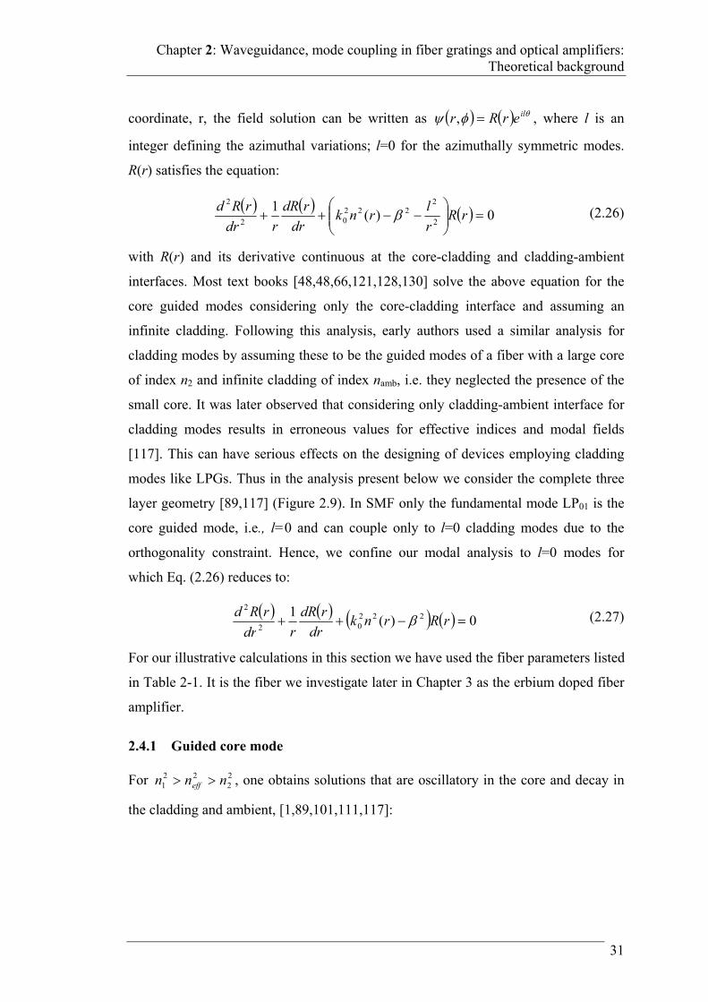
Chapter 2: Waveguidance, mode coupling in fiber gratings and optical amplifiers: Theoretical background
31
coordinate, r, the field solution can be written as ilerRr , , where l is an
integer defining the azimuthal variations; l=0 for the azimuthally symmetric modes.
R(r) satisfies the equation:
0)(1
2
2222
02
2
rR
r
lrnk
dr
rdR
rdr
rRd (2.26)
with R(r) and its derivative continuous at the core-cladding and cladding-ambient
interfaces. Most text books [48,48,66,121,128,130] solve the above equation for the
core guided modes considering only the core-cladding interface and assuming an
infinite cladding. Following this analysis, early authors used a similar analysis for
cladding modes by assuming these to be the guided modes of a fiber with a large core
of index n2 and infinite cladding of index namb, i.e. they neglected the presence of the
small core. It was later observed that considering only cladding-ambient interface for
cladding modes results in erroneous values for effective indices and modal fields
[117]. This can have serious effects on the designing of devices employing cladding
modes like LPGs. Thus in the analysis present below we consider the complete three
layer geometry [89,117] (Figure 2.9). In SMF only the fundamental mode LP01 is the
core guided mode, i.e., l=0 and can couple only to l=0 cladding modes due to the
orthogonality constraint. Hence, we confine our modal analysis to l=0 modes for
which Eq. (2.26) reduces to:
0)(1 222
02
2
rRrnkdr
rdR
rdr
rRd (2.27)
For our illustrative calculations in this section we have used the fiber parameters listed
in Table 2-1. It is the fiber we investigate later in Chapter 3 as the erbium doped fiber
amplifier.
2.4.1 Guided core mode
For 22
221 nnn eff , one obtains solutions that are oscillatory in the core and decay in
the cladding and ambient, [1,89,101,111,117]:
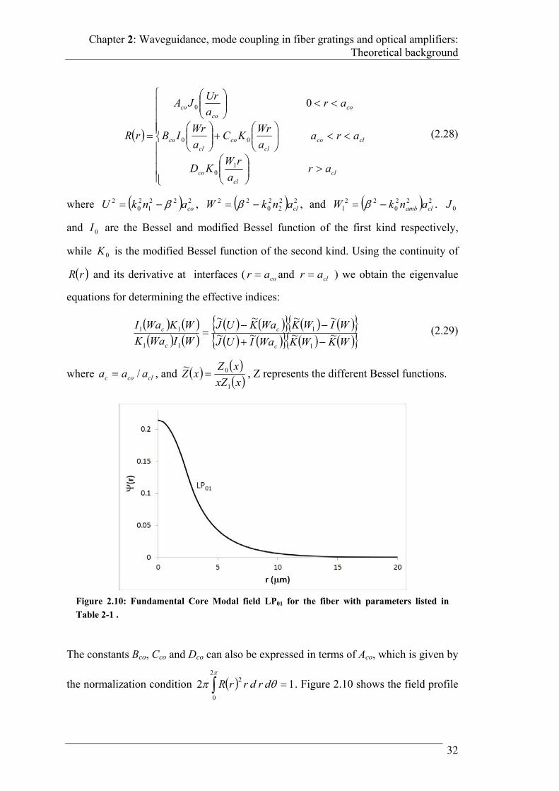
Chapter 2: Waveguidance, mode coupling in fiber gratings and optical amplifiers: Theoretical background
32
clcl
co
clcocl
cocl
co
coco
co
ara
rWKD
araa
WrKC
a
WrIB
ara
UrJA
rR
10
00
0 0
(2.28)
where 2221
20
2coankU , 22
220
22clankW , and 222
022
1 clamb ankW . 0J
and 0I are the Bessel and modified Bessel function of the first kind respectively,
while 0K is the modified Bessel function of the second kind. Using the continuity of
rR and its derivative at interfaces ( coar and clar ) we obtain the eigenvalue
equations for determining the effective indices:
WKWKWaIUJ
WIWKWaKUJ
WIWaK
WKWaI
c
c
c
c~~~~
~~~~
1
1
11
11
(2.29)
where clcoc aaa / , and xxZ
xZxZ
1
0~ , Z represents the different Bessel functions.
The constants Bco, Cco and Dco can also be expressed in terms of Aco, which is given by
the normalization condition 122
0
2
drdrrR . Figure 2.10 shows the field profile
Figure 2.10: Fundamental Core Modal field LP01 for the fiber with parameters listed in
Table 2-1 .
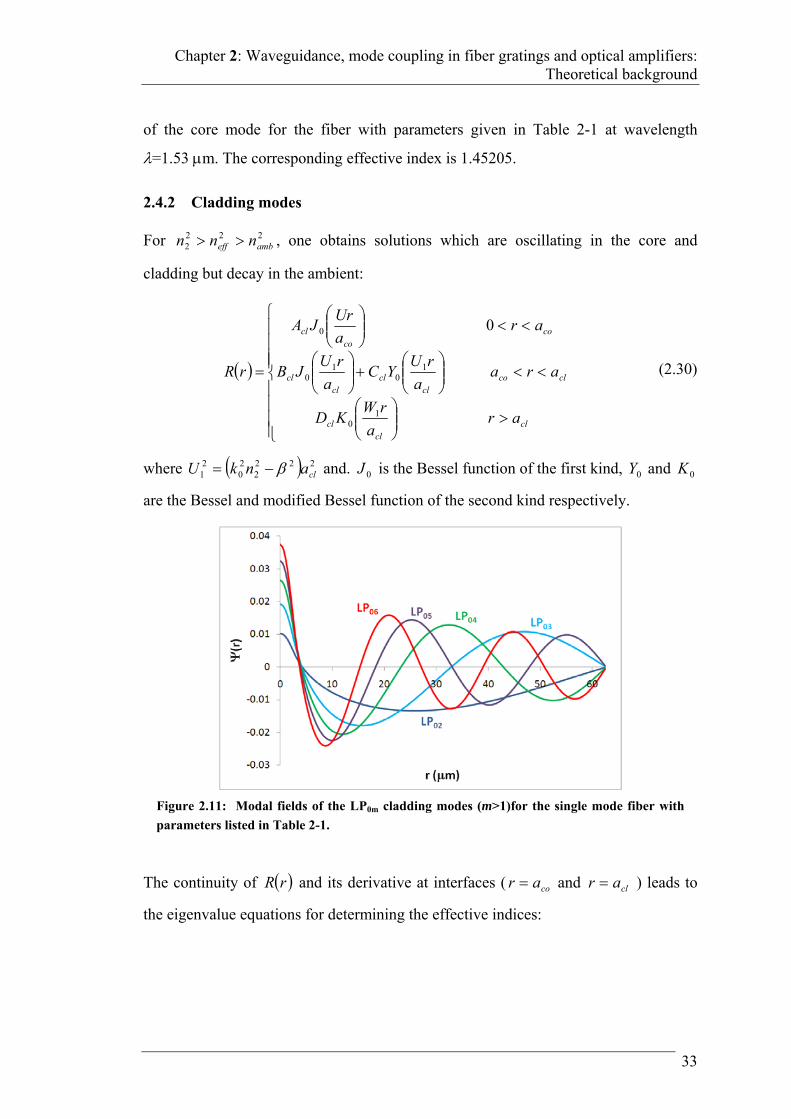
Chapter 2: Waveguidance, mode coupling in fiber gratings and optical amplifiers: Theoretical background
33
of the core mode for the fiber with parameters given in Table 2-1 at wavelength
=1.53 m. The corresponding effective index is 1.45205.
2.4.2 Cladding modes
For 2222 ambeff nnn , one obtains solutions which are oscillating in the core and
cladding but decay in the ambient:
clcl
cl
clcocl
clcl
cl
coco
cl
ara
rWKD
araa
rUYC
a
rUJB
ara
UrJA
rR
10
10
10
0 0
(2.30)
where 2222
20
21 clankU and. 0J is the Bessel function of the first kind, 0Y and 0K
are the Bessel and modified Bessel function of the second kind respectively.
The continuity of rR and its derivative at interfaces ( coar and clar ) leads to
the eigenvalue equations for determining the effective indices:
Figure 2.11: Modal fields of the LP0m cladding modes (m>1)for the single mode fiber with
parameters listed in Table 2-1.

Chapter 2: Waveguidance, mode coupling in fiber gratings and optical amplifiers: Theoretical background
34
111
111
1111
1111~~~~
~~~~
UYWKUJaUJ
UJWKUJaUY
UJaUY
UYaUJ
c
c
c
c
(2.31)
Again Bcl, Ccl and Dcl can be expressed in terms of Acl, which is obtained by the
normalization condition. Figure 2.11 shows the modal field profile of different
cladding modes for the fiber with the parameters given in Table 2-1, at =1.53 m .
The corresponding effective indices are tabulated in the last column of Table 2-2.
2.4.3 Comment on considering only the cladding-ambient interface for cladding
modes
As mentioned earlier, some early authors used the two layer geometry in refractive
index given by:
clamb
cl
arn
arnrn
0)( 2 (2.32)
for obtaining the propagation characteristics of cladding modes. The solution of this
geometry is well known and is given by [48,48,66,130]:
clcl
clcl
ara
rWK
WK
A
ara
rUJ
UJ
A
rR1
010
10
10
)(
)()( (2.33)
with 2222
20
21 )( clankU and the eigenvalue equation is given by:
Figure 2.12: (a) Two layer geometry for calculation of cladding modes. (b) Core index as
perturbation on the two layer geometry.
Chapter 2: Waveguidance, mode coupling in fiber gratings and optical amplifiers: Theoretical background
35
)(
)(
)(
)(
10
111
10
111 WK
WKW
UJ
UJU (2.34)
Since 1 and aco<< acl, the core refractive index region can be treated as a small
perturbation to the two-layer geometry to correct the effective indices of cladding
modes. The index perturbation 2n will be defined as:
co
co
ar
arnnn
0
22
212 (2.35)
and the first order perturbation correction to 2effn is obtained as:
fraca
eff PnrdrRnnco
2
0
20
22 2 (2.36)
where fracP is the fractional power of the cladding mode in the core region. Using the
modal field expression (2.33) for the field and the eigenvalue equation, the fractional
power of the cladding mode in core can be expressed analytically as:
32
1320
320
2 UaJUaJUJ
aAP cc
cofrac
(2.37)
We carried out calculations for the same fiber with parameters listed in Table 2-1. The
results of our calculations are summarized in Table 2-2.
It is interesting to note (Table 2-2) that the LP01 mode obtained from the two layer
geometry for the cladding modes, on taking into account the perturbation due to core,
falls in the region 22
221 nnn eff , i.e., it is no longer a cladding mode. Hence the first
modal solution in the two layer geometry should be ignored and the second solution
onwards should be used to approximate the LP0m (m>1) cladding modes of the actual
fiber.
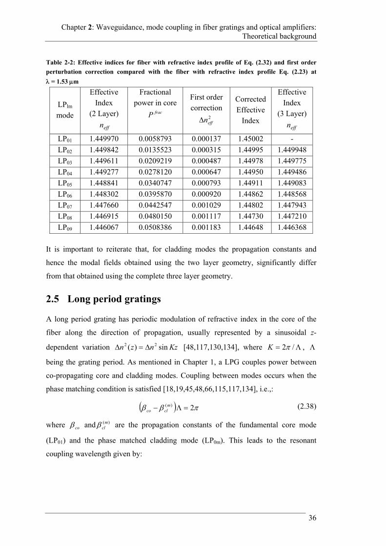
Chapter 2: Waveguidance, mode coupling in fiber gratings and optical amplifiers: Theoretical background
36
Table 2-2: Effective indices for fiber with refractive index profile of Eq. (2.32) and first order
perturbation correction compared with the fiber with refractive index profile Eq. (2.23) at
= 1.53 m
LPlm mode
Effective Index
(2 Layer)
effn
Fractional power in core
fracP
First order correction
2effn
Corrected Effective
Index
Effective Index
(3 Layer)
effn
LP01 1.449970 0.0058793 0.000137 1.45002 -
LP02 1.449842 0.0135523 0.000315 1.44995 1.449948
LP03 1.449611 0.0209219 0.000487 1.44978 1.449775
LP04 1.449277 0.0278120 0.000647 1.44950 1.449486
LP05 1.448841 0.0340747 0.000793 1.44911 1.449083
LP06 1.448302 0.0395870 0.000920 1.44862 1.448568
LP07 1.447660 0.0442547 0.001029 1.44802 1.447943
LP08 1.446915 0.0480150 0.001117 1.44730 1.447210
LP09 1.446067 0.0508386 0.001183 1.44648 1.446368
It is important to reiterate that, for cladding modes the propagation constants and
hence the modal fields obtained using the two layer geometry, significantly differ
from that obtained using the complete three layer geometry.
2.5 Long period gratings
A long period grating has periodic modulation of refractive index in the core of the
fiber along the direction of propagation, usually represented by a sinusoidal z-
dependent variation Kznzn sin)( 22 [48,117,130,134], where /2K ,
being the grating period. As mentioned in Chapter 1, a LPG couples power between
co-propagating core and cladding modes. Coupling between modes occurs when the
phase matching condition is satisfied [18,19,45,48,66,115,117,134], i.e.,:
2)( mclco (2.38)
where co and )(mcl are the propagation constants of the fundamental core mode
(LP01) and the phase matched cladding mode (LP0m). This leads to the resonant
coupling wavelength given by:
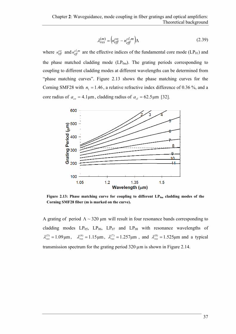
Chapter 2: Waveguidance, mode coupling in fiber gratings and optical amplifiers: Theoretical background
37
mcleff
coeff
mres nn ,)( (2.39)
where coeffn and mcl
effn , are the effective indices of the fundamental core mode (LP01) and
the phase matched cladding mode (LP0m). The grating periods corresponding to
coupling to different cladding modes at different wavelengths can be determined from
“phase matching curves”. Figure 2.13 shows the phase matching curves for the
Corning SMF28 with 46.11 n , a relative refractive index difference of 0.36 %, and a
core radius of μm1.4coa , cladding radius of μm5.62cla [32].
A grating of period μm320~ will result in four resonance bands corresponding to
cladding modes LP05, LP06, LP07 and LP08 with resonance wavelengths of
μm09.1)5( res , μm15.1)6( res , μm257.1)7( res , and μm525.1)8( res and a typical
transmission spectrum for the grating period 320 m is shown in Figure 2.14.
Figure 2.13: Phase matching curve for coupling to different LP0m cladding modes of the
Corning SMF28 fiber (m is marked on the curve).
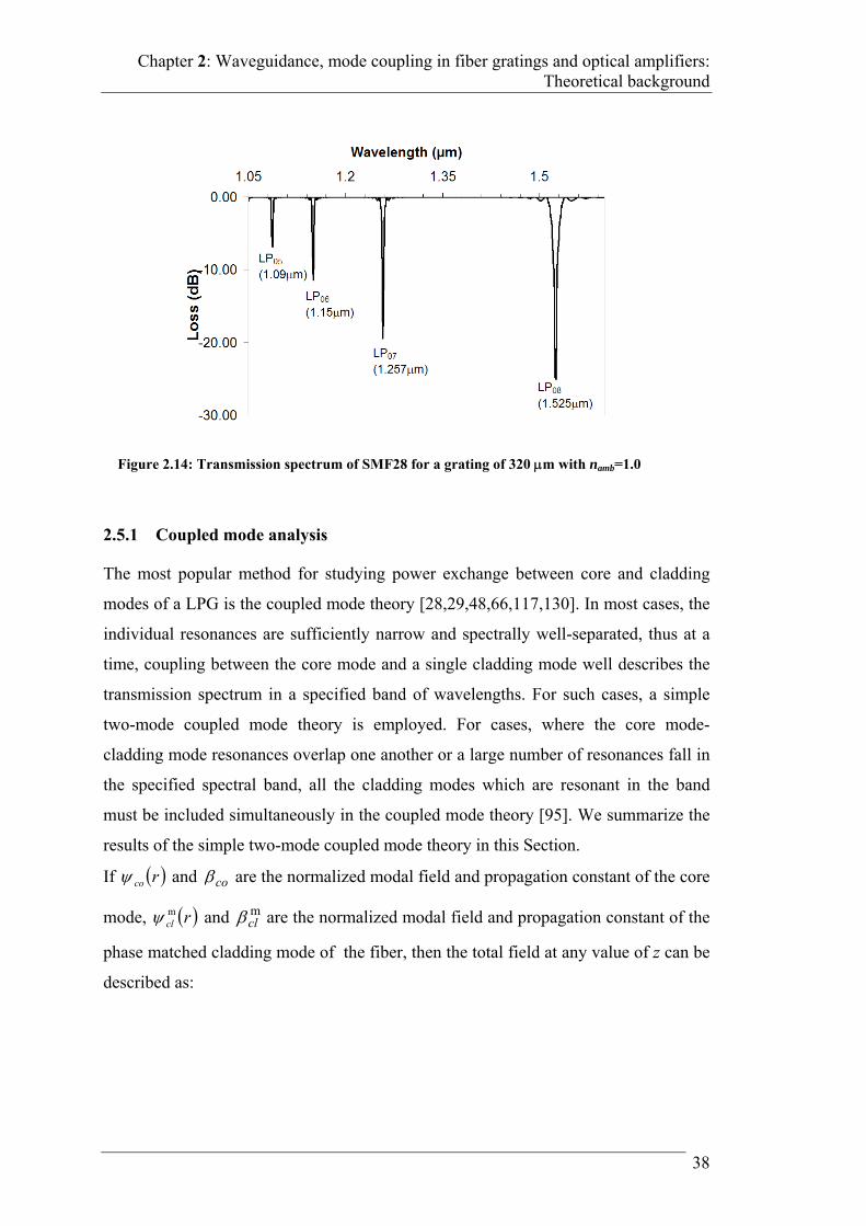
Chapter 2: Waveguidance, mode coupling in fiber gratings and optical amplifiers: Theoretical background
38
2.5.1 Coupled mode analysis
The most popular method for studying power exchange between core and cladding
modes of a LPG is the coupled mode theory [28,29,48,66,117,130]. In most cases, the
individual resonances are sufficiently narrow and spectrally well-separated, thus at a
time, coupling between the core mode and a single cladding mode well describes the
transmission spectrum in a specified band of wavelengths. For such cases, a simple
two-mode coupled mode theory is employed. For cases, where the core mode-
cladding mode resonances overlap one another or a large number of resonances fall in
the specified spectral band, all the cladding modes which are resonant in the band
must be included simultaneously in the coupled mode theory [95]. We summarize the
results of the simple two-mode coupled mode theory in this Section.
If rco and co are the normalized modal field and propagation constant of the core
mode, rclm and m
cl are the normalized modal field and propagation constant of the
phase matched cladding mode of the fiber, then the total field at any value of z can be
described as:
Figure 2.14: Transmission spectrum of SMF28 for a grating of 320 m with namb=1.0

Chapter 2: Waveguidance, mode coupling in fiber gratings and optical amplifiers: Theoretical background
39
zicl
zico
clco erzBerzAmm)()( (2.40)
Following the analysis in various text books [48, ,121,122], in the slowly varying
approximation coupled differential equations which describe the change of amplitudes
with propagation distance are obtained as:
zizKi ezBezBdz
zdA 1212 (2.41)
zizKi ezAezAdz
zdB 2121 (2.42)
where drrnk
cl
a
coco
m
0
220
12 2
, drrnk
co
a
clcl
0
2mm
20
21 2 and Γ known as
detuning or phase mismatch factor is defined as
22 )(, mcl
effcoeff nn (2.43)
Differentiating equation (2.41) with respect to z and using (2.42), we obtain a second
order differential equation for A:
022
2
zAdz
zdAi
dz
zAd (2.44)
where 2112 is the coupling coefficient.
Employing the boundary conditions that A(z=0)=A0 and B(z=0)=B0, we obtain the
following analytical solutions for A(z) and B(z) :
)sin()sin(2
)cos( 002 ziBzizAezAzi
)zsin(i)zcos(B)zsin(iAezB
zi
2002
(2.45)
where 22
4 . If we assume that power is initially launched only in the core
mode, i.e., A (z=0)=1 and B(z=0)=0 and the above equations reduce to a following
simplified form:
Chapter 2: Waveguidance, mode coupling in fiber gratings and optical amplifiers: Theoretical background
40
)sin(2
)cos(2 zizezAzi
)zsin(iezBzi
2
(2.46)
The power in the core mode and the cladding mode at any z can now be expressed as:
zzAzAzPco 2
2
2
sin1
zzBzBzPcl 2
2
2
sin
(2.47)
At phase matching wavelength the detuning factor 0 and . Hence, the
power in the core mode and cladding mode can be expressed as:
zzPco 2sin1
zzPcl 2sin (2.48)
Power is continuously exchanged between the core mode and the phase matched
cladding mode and complete power transfer occurs at coupling length cl is given by:
2
cl (2.49)
In Section 2.4.3 we briefly commented on the use of two layer geometry for
characterizing the cladding modes and tabulated the error introduced by this
simplified picture in calculations for the fiber with parameter given in Table 2-1. To
further emphasize the necessity of using complete all the three layers for the
characterizing the cladding modes we also investigate the transmission spectrum
obtained by the two calculations. We consider a LPG written in the fiber with
parameters given in Table 2-1. With index modulation 42 102 n and
μm297 . A two layer calculation predicts μm53.1res for the LP01-LP09
coupling while the correct μm438.1res . The transmission spectrum for a grating of
length 4.6 cm, calculated by the two layer geometry shows a complete resonance at
1.53 m, while the correct spectrum shows an incomplete resonance at 1.438 m.
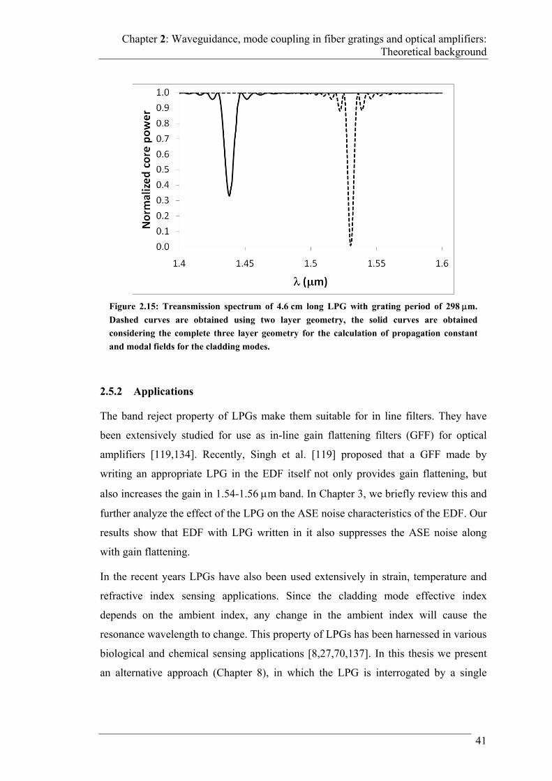
Chapter 2: Waveguidance, mode coupling in fiber gratings and optical amplifiers: Theoretical background
41
2.5.2 Applications
The band reject property of LPGs make them suitable for in line filters. They have
been extensively studied for use as in-line gain flattening filters (GFF) for optical
amplifiers [119,134]. Recently, Singh et al. [119] proposed that a GFF made by
writing an appropriate LPG in the EDF itself not only provides gain flattening, but
also increases the gain in 1.54-1.56 m band. In Chapter 3, we briefly review this and
further analyze the effect of the LPG on the ASE noise characteristics of the EDF. Our
results show that EDF with LPG written in it also suppresses the ASE noise along
with gain flattening.
In the recent years LPGs have also been used extensively in strain, temperature and
refractive index sensing applications. Since the cladding mode effective index
depends on the ambient index, any change in the ambient index will cause the
resonance wavelength to change. This property of LPGs has been harnessed in various
biological and chemical sensing applications [8,27,70,137]. In this thesis we present
an alternative approach (Chapter 8), in which the LPG is interrogated by a single
Figure 2.15: Treansmission spectrum of 4.6 cm long LPG with grating period of 298 m.
Dashed curves are obtained using two layer geometry, the solid curves are obtained
considering the complete three layer geometry for the calculation of propagation constant
and modal fields for the cladding modes.
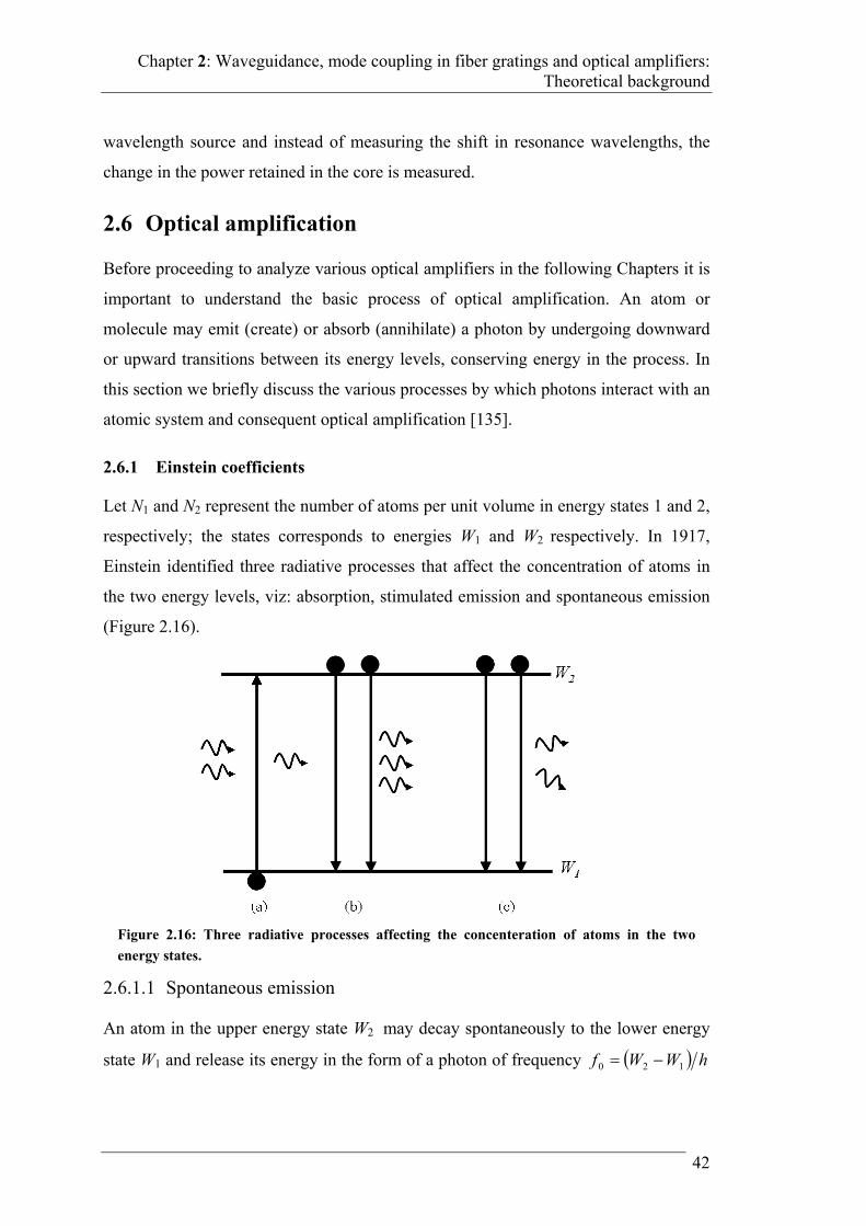
Chapter 2: Waveguidance, mode coupling in fiber gratings and optical amplifiers: Theoretical background
42
wavelength source and instead of measuring the shift in resonance wavelengths, the
change in the power retained in the core is measured.
2.6 Optical amplification
Before proceeding to analyze various optical amplifiers in the following Chapters it is
important to understand the basic process of optical amplification. An atom or
molecule may emit (create) or absorb (annihilate) a photon by undergoing downward
or upward transitions between its energy levels, conserving energy in the process. In
this section we briefly discuss the various processes by which photons interact with an
atomic system and consequent optical amplification [135].
2.6.1 Einstein coefficients
Let N1 and N2 represent the number of atoms per unit volume in energy states 1 and 2,
respectively; the states corresponds to energies W1 and W2 respectively. In 1917,
Einstein identified three radiative processes that affect the concentration of atoms in
the two energy levels, viz: absorption, stimulated emission and spontaneous emission
(Figure 2.16).
2.6.1.1 Spontaneous emission
An atom in the upper energy state W2 may decay spontaneously to the lower energy
state W1 and release its energy in the form of a photon of frequency hWWf 120
Figure 2.16: Three radiative processes affecting the concenteration of atoms in the two
energy states.
Chapter 2: Waveguidance, mode coupling in fiber gratings and optical amplifiers: Theoretical background
43
(Figure 2.16 c). The process is called spontaneous emission. The emitted photon has a
random phase and direction. The spontaneous emission rate (number of spontaneous
transitions per unit time per unit volume) from state 2 to state 1 is given by:
221NARsp (2.50)
where A21 is the Einstein’s A coefficient for the transition from state 2 to state 1.
Hence, only due to spontaneous emission 2212 NA
dt
dN which simplifies to
spteNtN /22 0 where 211 Asp is the spontaneous lifetime of state 2.
2.6.1.2 Absorption
When a photon of energy 12 WWhfW impinges on the atomic system, an atom
in the lower energy level W1 can absorb the energy and make an upward transition to
upper energy level W2 (Figure 2.16 a). The rate at which this process takes place must
depend on the density of absorbing atoms (N1) as well as the energy density of the
incident photons, fPh , at the center frequency f, and is given by:
fNBR Phastim 112 (2.51)
where B12 is the Einstein B coefficient for transition from energy state 1 to state 2. If
NPh denotes the number of photons per unit volume at frequency f, then
hfNf PhPh
2.6.1.3 Stimulated emission
An atom in the upper energy level W2, can be induced by the impinging photons, to
make a downward transition to lower energy level W1 (Figure 2.16 b). This process is
called stimulated or induced emission, since it is induced by the presence of photons.
The emitted photon is at the same frequency, same phase, and same polarization and
propagates in the same direction as the photon that induced the atom to undergo this
type of transition. The rate of stimulated emission will depend on the density of atoms
in the upper energy level and the energy density of the incident photons.
Chapter 2: Waveguidance, mode coupling in fiber gratings and optical amplifiers: Theoretical background
44
fNBR Phestim 221 (2.52)
where B21 is the Einstein B coefficient for transition from energy state 2 to state 1.
2.6.1.4 Relationship between Einstein coefficients
Let us consider a cavity of volume AdzV . Under thermal equilibrium, the energy
density of photons at frequency f, in the cavity is given by Planck’s blackbody
radiation expression:
1
83
22
Tkhf
gPh
Be
hf
c
fnnf
(2.53)
where n is the refractive index of the medium, ng is the group index defined as:
d
dnnng (2.54)
Under thermal equilibrium, the rate of upward transitions, defined by Eq (2.51),
should be equal to the downward transitions, defined by Eqs. (2.50) and (2.52). Thus
we may write:
fNBfNBNA PhPh 112221221
or 21
2
112
21
BN
NB
AfPh
(2.55)
The atoms in the cavity at thermal equilibrium follow Boltzmann distribution i.e.
Tk
hf
Beg
g
N
N
1
2
1
2 , where )1(2g is the degeneracy of the energy2 state )1(2W . Comparing
the above relation with the Eq. (2.53) for the energy density of incident radiation,
gives:
2 For a simple atom the quantity g2(1) is related to the total angular momentum number J2(1) by g2(1)=2J2(1)+1
Chapter 2: Waveguidance, mode coupling in fiber gratings and optical amplifiers: Theoretical background
45
121212 BgBg
and hfnc
n
c
hfnn
B
A gg 223
32
21
21 818
(2.56)
where fc / is the wavelength of the electromagnetic wave. The importance of
these relations lies in the fact that it if one of the coefficients is known, the others can
be evaluated.
It is very important to realize that Einstein coefficients are characteristics of an atom.
The atom has no way to know whether it is in a thermodynamic equilibrium
environment of a cavity or in the presence of an intense optical field (a laser)
generated by other atoms. It responds to an electromagnetic radiation as determined
by Eqs. (2.50-2.52). Hence these relations are always valid.
2.6.2 Optical gain
We now describe the process of amplification of radiation by its interaction with the
atom. Photon flux f is defined as the number of photons crossing per unit area per
unit time, i.e., cnNf gPh / . Eq. (2.51) and (2.52) describe the number of upward
and downward transitions respectively, in response to the photon flux, f . The net
increase in the photon flux per unit length along the z-direction is determined by the
difference between stimulated emission and absorption rates:
fBNg
gNRR
dz
fd astim
estim
2111
22
(2.57)
From this relation we can see that there is net optical gain only if 11
22 N
g
gN , i.e.,
population inversion is necessary for optical amplification. Population inversion does
not occur naturally, some external means is needed to create this state of population
inversion. We can achieve population inversion either by pumping by another optical
source (as in EDFA and EDWA), or by electrical injection (as in SOAs).
The optical gain of the medium is the fractional increase in photon flux per unit length
is given by [147]:
Chapter 2: Waveguidance, mode coupling in fiber gratings and optical amplifiers: Theoretical background
46
dz
fd
ffg
1 (2.58)
Thus, the optical gain at signal frequency f is obtained as:
1
1
2221 N
g
gNBhf
c
nfg g (2.59)
2.6.3 Spectral broadening
The above analysis assumed sharp energy levels involved in the transition. However,
from uncertainty principle we know that there is no such thing as precise energy state,
which implies it is not possible to have all the transitions at exactly f such that
12 WWhf . Instead the real systems emit a narrow band of frequencies whose
width f is much less than the center frequency f.
In the real system, we have a distribution of energies around levels W1 and W2. There
can be transitions from the manifold W2 to manifold W1 at various frequencies
centered around f. The broadening of each energy level can be different and may or
may not be symmetrical. Thus, there exists a distribution of photon frequencies that
can be emitted spontaneously. This relative distribution is called the line shape
function fL . dffL gives the probability that a given transition between the two
energy levels will result in the emission (or absorption) of a photon whose frequency
lies between f and f +df. Thus dfff L determines the energy density of photons
causing the transitions between f and f+df. Here we should also mention that lineshape
function is normalized, i.e.
1dffL .
In this thesis, we are mainly dealing with monochromatic sources/signals, i.e., only
one frequency. For such signals the spectral width of f is very small compared to
fL , thus f can be approximated by a function:
Chapter 2: Waveguidance, mode coupling in fiber gratings and optical amplifiers: Theoretical background
47
fff f '' (2.60)
Thus the net increase in photon flux per unit length around center frequency f in the
interval df will be given by integrating over the all the range of transitions covered in
the frequency interval df [147]:
dfffNg
gNB
c
nRR ga
stimestim L
1
1
2221 (2.61)
To avoid confusion, we use to represent the optical gain including the spectral
broadening:
11
2221
1N
g
gNfhfB
c
ndffgf
dz
fd
ff g LL
(2.62)
The quantity in curly braces has the dimension of area (m2) and is referred to as the
stimulated emission cross section fe .
fhfBc
nf g
e L21 (2.63)
In similar fashion we also define absorption cross section fa as:
fg
gf ea
1
2 (2.64)
In terms of absorption and emission cross-section the gain coefficient can be written
as:
12 NfNff ae (2.65)
Lasers and optical amplifiers are the two important optical devices based on the
amplification of light by stimulated emission. While lasers generate optical signals,
optical amplifiers amplify an optical signal in the optical domain.
It is more common to express change in intensity or power as light propagates through
the gain medium in terms of gain coefficient. Let If be the intensity of irradiated light
of frequency f (considering monochromatic source), it depends on both the photon
flux f and photon energy hf, hffI f . We can determine the increase
(decrease) in intensity as it passes through the gain (loss) medium using Eq. (2.62) as:
Chapter 2: Waveguidance, mode coupling in fiber gratings and optical amplifiers: Theoretical background
48
ff If
dz
dI (2.66)
2.6.4 Types of optical amplifiers
Optical amplifiers amplify an optical signal without any conversion of light into
electrical signal. Though, the first generation of optical amplifiers was developed in
1960 using a Neodymium doped fiber [74,120], a major breakthrough in optical
amplification came about twenty years later. In 1985, at Southampton University
David Payne and his colleagues reported a high gain fiber amplifier using erbium
doped silica fiber [83,84]. It provided new life to the optical fiber low loss
transmission window centered at 1.55 m and motivated research into technologies
like wavelength division multiplexing (WDM), that allow high bit rate transmission
over long distances. The success of EDFA led to the development of many alternative
amplifier technologies. While, EDFA remains the choice for long haul communication
system, due to small size and ease of integration, deployment of semiconductor optical
amplifiers in optical networks is increasing. In this section, we briefly describe some
important optical amplifiers.
2.6.4.1 Erbium doped fiber amplifiers
EDFA typically consists of an erbium doped fiber gain medium, a pump laser (980 nm
or 1480 nm) to excite the gain medium and couplers to couple the pump and signal
powers to the erbium doped fiber. The pump can be coupled at either end of the fiber
resulting in either co-propagating or counter-propagating pump. The erbium ions
present in the fiber core are excited to a high energy state by the pump. When photons
from the input signal in the range of about 1.53-1.60 m strike the excited erbium
ions, some of erbium ions return to a lower energy state transferring the energy to the
optical signal. This results in amplification of the optical signal via stimulated
emission. The EDFA has many desirable features the most important being that it
amplifies in the 1.55 m wavelength window where fiber loss is minimum. It provides
a gain bandwidth of 40 nm, which implies that it can amplify many channels
simultaneously in the C-band, making it a key device in WDM/DWDM technology.
Chapter 2: Waveguidance, mode coupling in fiber gratings and optical amplifiers: Theoretical background
49
EDFA has two major disadvantages, the first being its non-uniform gain spectrum.
The non-uniform amplification of WDM signals can cause signal distortion and poor
signal-to-noise ratio performance. This led to the development of various types of gain
flattening methods (GFF) [15,34,51,71,79,107,128,143].
The second disadvantage of EDFA is the amplification of spontaneous emission
(ASE). ASE emerges from both ends of the doped fiber and must be dealt with. ASE
in the same direction as the signal is a major source of cumulative noise (reducing
signal to noise ratio), while backward propagating ASEs can harm source lasers if not
filtered out. The presence of ASE also reduces the available optical gain for the signal
field. Though undesirable, spontaneous emission is an inherent process of optical
amplification and hence, ASE cannot be eliminated completely. Many methods have
been explored to mitigate ASE, like using filters or isolators [15,34].
Besides erbium, other rare earth elements have also been used to provide gain in
different wavelength regions [69]: Praseodymium (around 1.3 m), Neodymium
(around 1 m) [78] and Thulium in the S-band (1.45-1.50 m) [109]. The design and
operation of such amplifiers is, in principle, quite similar to that of the EDFA,
although they require different pump wavelengths and typically much higher pump
powers.
2.6.4.2 Erbium doped waveguide amplifiers
The need for small size and great functionality optical components motivated interest
in the erbium doped waveguide amplifiers (EDWA). EDWAs offer several advantages
over EDFAs: They are of low cost and small size and allow integration of passive
components like couplers etc on the same chip. In order to achieve same gain values
in short length (few cm), the EDWAs require high erbium ion concentration. The high
erbium ions concentration has some limitations, as the erbium ion concentration
increases the ions come closer this increases the probability of the formation of
clusters. When excited, the erbium ions in the clusters start exchanging energy this
reduces their efficiency.
A lot of attention is focused on lithium niobate (LiNbO3) waveguides doped with
erbium [52,63]. These waveguides can be obtained from a variety of procedures, the
Chapter 2: Waveguidance, mode coupling in fiber gratings and optical amplifiers: Theoretical background
50
most common being titanium diffusion. These waveguides are pumped by 1484 nm
radiation and provide amplification around 1.53 m.
2.6.4.3 Semiconductor optical amplifiers
Semiconductor optical amplifier (SOA) is essentially a semiconductor laser with no
reflecting facets [31,147]. In EDFA, EDWG and Raman amplifiers the pump is
provided optically, but in a SOA an electrical current is used to excite the gain
medium (also called active region or active layer). A typical SOA has a p-doped
semiconductor layer, an n-doped semiconductor layer and a gain region (also called
active layer) sandwiched between the two. The p and n-doped semiconductor layers
have higher band gap and lower index of refraction than the active region. These
layers behave as a cladding and tend to confine the optical mode within active region.
The ends of the waveguide are usually treated to avoid optical feedback. An anti-
reflective coating is often applied to the facets to decrease the reflection. When an
optical signal is injected from the input facet, the light is amplified by the gain of the
active layer. The gain spectrum of an SOA strongly depends on the bandgap of the
semiconductor constituting the active region. Due to their compact size, reduced
power consumption and reduced cost of fabrication, semiconductor optical amplifiers
have begun to replace EDFAs in Metro access and local access networks. The
disadvantages of SOAs include much narrower wavelength bands, reduced
amplification, and higher noise figure than erbium-doped optical amplifiers
The SOAs can also be used to perform different processing tasks [30,31,91] in all
optical networks. Most of these functional applications are based on SOA
nonlinearities. The main reason for nonlinearity of an SOA is that the gain of the SOA
depends on the input signal. The four main types of nonlinearities are:
Cross gain modulation (XGM): When the strong signal at one wavelength affects the
gain of a weak signal at another wavelength.
Cross phase modulation (XPM): When the refractive index changes induced by a
strong optical signal at one wavelength affect the output phase of a weak signal at
another wavelength.
Chapter 2: Waveguidance, mode coupling in fiber gratings and optical amplifiers: Theoretical background
51
Self phase modulation (SPM): When the refractive index change induced by a signal
affects the output phase of the same signal.
Four wave mixing (FWM): When the mixing of two or more signals propagating
along the SOA generate optical signal at new frequencies.
These nonlinearities of an SOA can be exploited to implement functions like
wavelength conversion, optical switches, optical logic gates, and multiplexers.
2.6.4.4 Raman amplifiers
The discussion on types of optical amplifiers will be incomplete without the
discussion of Raman amplifiers. The principle of Raman amplifiers is not same as
other amplifiers (EDFA, EDWG or SOAs), instead the amplification is achieved by a
nonlinear interaction between the signal and a pump laser within an optical fiber, the
stimulated Raman scattering (SRS). The process of SRS generates scattered light at a
wavelength longer than that of the incident light (pump wavelength). If another signal
is present at this longer wavelength, the SRS light will amplify it
Each Raman amplifier may contain one or more pumps. Raman amplifiers can easily
adjust the amplification band by properly choosing the wavelength of the pumping
light. Raman amplifiers are becoming increasingly important in optical
communication systems, particularly, in high-bit rate WDM/DWDM systems. An
important advantage of Raman amplification is that the signal-to-noise ratio is much
lower than that of an EDFA having the same gain. Raman amplifiers can cover a
much wider spectral range than rare-earth based amplifiers. Furthermore, Raman
amplifiers have lower noise levels than rare-earth amplifiers. These advantages make
Raman amplifiers desirable for long haul WDM systems where the transmission
bandwidth may be broad. However, the Raman amplifier not only has very low optical
amplification efficiency but also needs a high power pump source, thereby increasing
the entire size of the optical amplifier module and the price of the optical amplifier
module
Chapter 2: Waveguidance, mode coupling in fiber gratings and optical amplifiers: Theoretical background
52
2.7 Summary
In this chapter we reviewed the basic electromagnetic theory needed to understand the
propagation of light in integrated optical waveguides and optical fibers. The chapter
started with the review of Maxwell equations. Variational method for the analysis of
diffused channel waveguides was briefly discussed. The solution for the core and
cladding modes using the complete three layers was reviewed.
In the end we discussed the basic physics involved in the process of optical
amplification, and finally described some popular optical amplifiers.
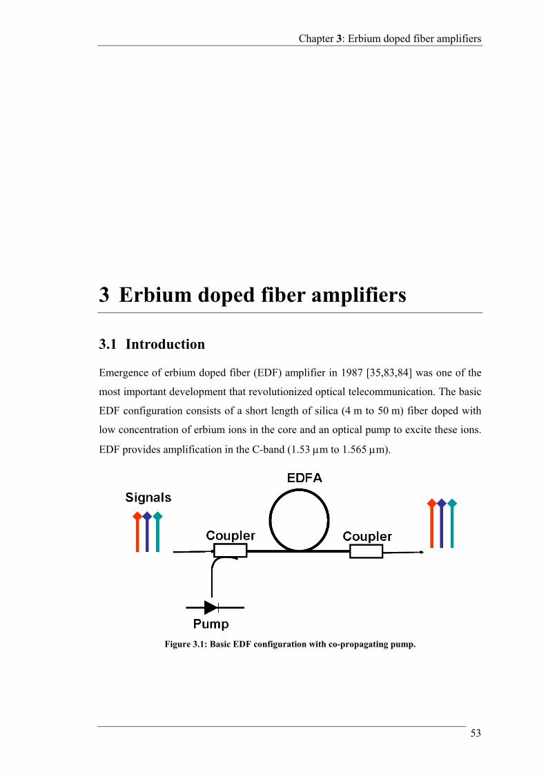
Chapter 3: Erbium doped fiber amplifiers
53
3 Erbium doped fiber amplifiers
3.1 Introduction
Emergence of erbium doped fiber (EDF) amplifier in 1987 [35,83,84] was one of the
most important development that revolutionized optical telecommunication. The basic
EDF configuration consists of a short length of silica (4 m to 50 m) fiber doped with
low concentration of erbium ions in the core and an optical pump to excite these ions.
EDF provides amplification in the C-band (1.53 m to 1.565 m).
Figure 3.1: Basic EDF configuration with co-propagating pump.
Chapter 3: Erbium doped fiber amplifiers
54
Figure 3.1 shows the typical configuration of an erbium doped fiber amplifier. A
wavelength selective coupler at the input combines the input signal and the pump
signal (typically at a wavelength of 980 nm or 1480 nm). The coupler at the output
separates the amplified signal from the residual pump power. EDF can amplify many
wavelength channels within its gain band. Thus, one can use a single amplifier for all
wavelengths in wavelength division multiplexed (WDM) systems.
However, EDF suffers from some limitations; the first is that the gain is not same for
all signal wavelengths. This is a problem for WDM systems, as it can result in signal
imbalance. The second is the presence of amplified spontaneous emission noise. It
emerges from both ends of the doped fiber and must be dealt with. ASE in the same
direction as the signal is a major source of cumulative noise (reducing signal to noise
ratio), while backward propagating ASEs can harm source lasers if not filtered out.
The presence of ASE also reduces the available optical gain for the signal field.
Various techniques have been proposed to flatten the gain spectrum. One of the
popular technique for gain flattening is the use of an external optical gain flattening
filter (GFF) having a loss profile that is reverse of the gain spectra of EDF
[51,107,143]. Singh et al. [119] proposed an alternative technique of gain flattening by
an appropriately chosen long period grating written through a length of the EDF itself.
The LPG was chosen so as to couple the 1.53 m wavelength experiencing peak gain
into the cladding; thus inversion in core is made available to other wavelengths. As a
result, in this configuration, there was gain flattening as well as increase in the average
gain across the 1.54-1.56 m band. We expect that this GFF proposed should also
affect the ASE noise characteristics. The spontaneous emission generated into the
propagating mode in each small section of fiber has a random phase. LPG is a phase
sensitive device and hence, it is necessary to consider both the amplitude and phase of
the propagating modes. In this Chapter we present the methodology evolved by us to
incorporate the spontaneous emission generated in each small section of fiber along
with its random phase and study its amplification in the EDF with the LPG written in
it. For completeness, we first review several aspects of erbium doped fiber amplifiers;
specifically we delve into some basic physics, the principle of operation and device
performance in terms of gain flattening and noise response. Then we propose the
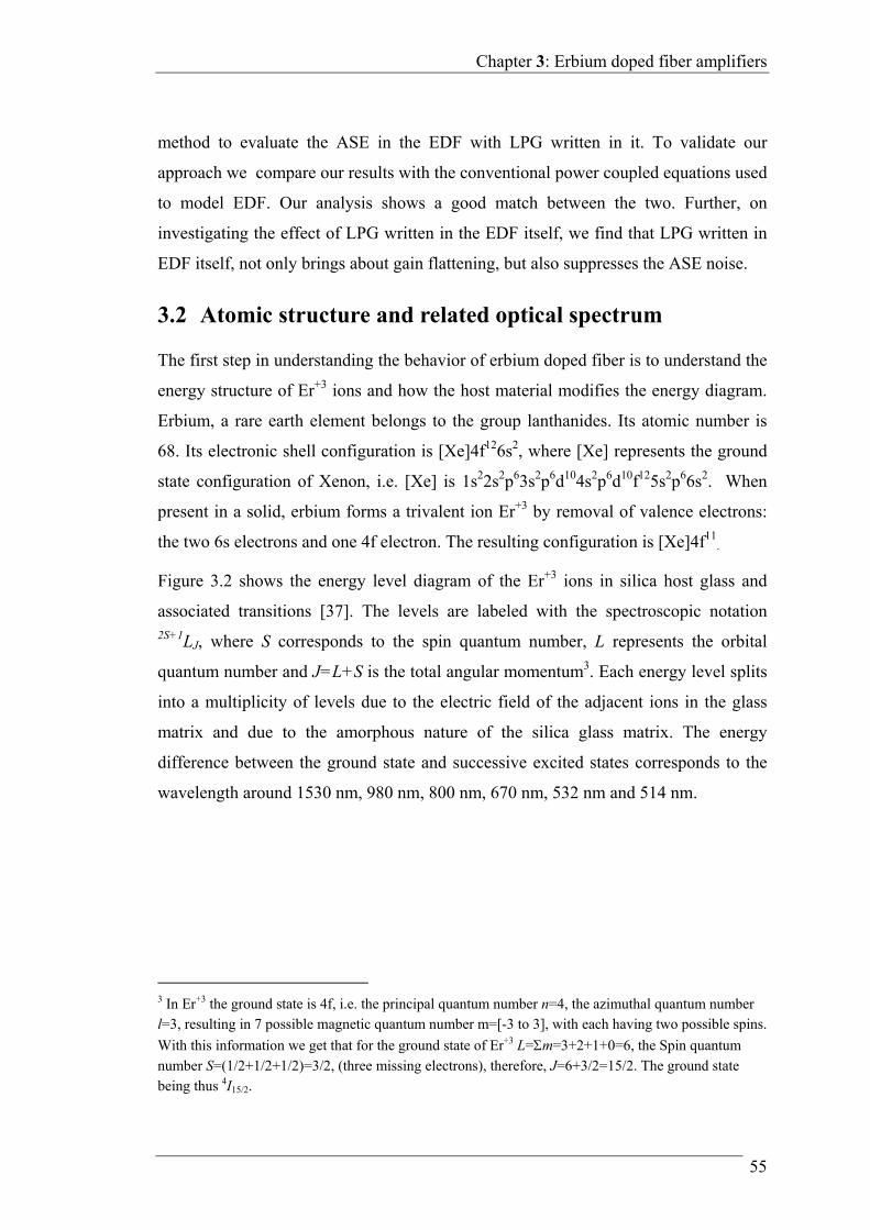
Chapter 3: Erbium doped fiber amplifiers
55
method to evaluate the ASE in the EDF with LPG written in it. To validate our
approach we compare our results with the conventional power coupled equations used
to model EDF. Our analysis shows a good match between the two. Further, on
investigating the effect of LPG written in the EDF itself, we find that LPG written in
EDF itself, not only brings about gain flattening, but also suppresses the ASE noise.
3.2 Atomic structure and related optical spectrum
The first step in understanding the behavior of erbium doped fiber is to understand the
energy structure of Er+3 ions and how the host material modifies the energy diagram.
Erbium, a rare earth element belongs to the group lanthanides. Its atomic number is
68. Its electronic shell configuration is [Xe]4f126s2, where [Xe] represents the ground
state configuration of Xenon, i.e. [Xe] is 1s22s2p63s2p6d104s2p6d10f125s2p66s2. When
present in a solid, erbium forms a trivalent ion Er+3 by removal of valence electrons:
the two 6s electrons and one 4f electron. The resulting configuration is [Xe]4f11.
Figure 3.2 shows the energy level diagram of the Er+3 ions in silica host glass and
associated transitions [37]. The levels are labeled with the spectroscopic notation 2S+1LJ, where S corresponds to the spin quantum number, L represents the orbital
quantum number and J=L+S is the total angular momentum3. Each energy level splits
into a multiplicity of levels due to the electric field of the adjacent ions in the glass
matrix and due to the amorphous nature of the silica glass matrix. The energy
difference between the ground state and successive excited states corresponds to the
wavelength around 1530 nm, 980 nm, 800 nm, 670 nm, 532 nm and 514 nm.
3 In Er+3 the ground state is 4f, i.e. the principal quantum number n=4, the azimuthal quantum number l=3, resulting in 7 possible magnetic quantum number m=[-3 to 3], with each having two possible spins.
With this information we get that for the ground state of Er+3 L=m=3+2+1+0=6, the Spin quantum
number S=(1/2+1/2+1/2)=3/2, (three missing electrons), therefore, J=6+3/2=15/2. The ground state being thus 4I15/2.

Chapter 3: Erbium doped fiber amplifiers
56
As shown in Figure 3.2, only the transitions between E2(4I13/2) and E1(
4I15/2) manifold
are radiative; all other relaxations are non-radiative. The lifetime of radiative
transition between E2(4I13/2) and E1(
4I15/2) is of the order of 10 ms, while the non-
radiative lifetime for the E3 to E2 transitions is 6.6 s. Thus Er+3 ions pumped by
980 nm wavelength from the ground state E1 (4I15/2) to an excited state E3 (
4I11/2), and
relax rapidly to a metastable state E2(4I13/2) which has a long lifetime. The ions at E2
decay radiatively (either spontaneous or stimulated) to the ground state E1. Population
Figure 3.2: Energy level diagram of Er+3 ions in silica host glass.

Chapter 3: Erbium doped fiber amplifiers
57
inversion is hence possible between levels E2 and E1 and hence, erbium ions in silica
host pumped by 980 nm radiation form a three level laser system.
3.2.1 Cross sections
The emission and absorption cross sections ae, defined in Eqs. (2.63) and (2.64)
characterize the E2-E1 manifold transitions. They are the fundamental parameters for
the EDF normally specified by the manufacturer [36]. For illustrative computations
we will use all the parameters corresponding to the erbium doped fiber codoped with
alumino silicate designated as Type III by Desurvire [34]. The variation of absorption
and emission cross sections of this Type III EDF with wavelengths are shown in
Figure 3.3. They are obtained from the following empirical formula [34] in the
1.4 to 1.6 m range:
i
ii
ipeak a
2ln4exp` (3.1)
where ia , i and i are the fitting parameters.. The typical values of these
parameters for type III EDF are tabulated in Table 3-1. The peak values (at
μm53.1 ) are given by 225 m100.7 peake and peakepeaka 92.0 . For the
pump wavelength of 980 nm, 225 m100.2 pa
Table 3-1: Fitting parameters for absorption and emission cross section
Absorption Emission
i ia i i ia i i
1 0.03 1.440 0.0400 0.06 1.470 0.0500
2 0.31 1.482 0.0500 0.16 1.500 0.0400
3 0.17 1.492 0.0290 0.30 1.520 0.0250
4 0.37 1.515 0.0290 0.73 1.530 0.0125
5 0.74 1.530 0.0165 0.38 1.542 0.0130
6 0.28 1.544 0.0170 0.49 1.556 0.0220
7 0.30 1.555 0.0250 0.20 1.575 0.0250
8 0.07 1.570 0.0350 0.06 1.600 0.0600
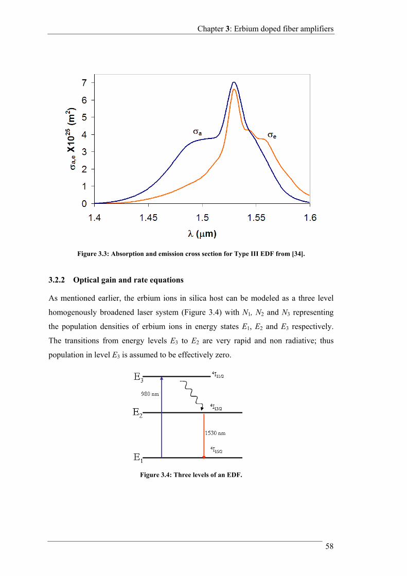
Chapter 3: Erbium doped fiber amplifiers
58
3.2.2 Optical gain and rate equations
As mentioned earlier, the erbium ions in silica host can be modeled as a three level
homogenously broadened laser system (Figure 3.4) with N1, N2 and N3 representing
the population densities of erbium ions in energy states E1, E2 and E3 respectively.
The transitions from energy levels E3 to E2 are very rapid and non radiative; thus
population in level E3 is assumed to be effectively zero.
Figure 3.3: Absorption and emission cross section for Type III EDF from [34].
Figure 3.4: Three levels of an EDF.
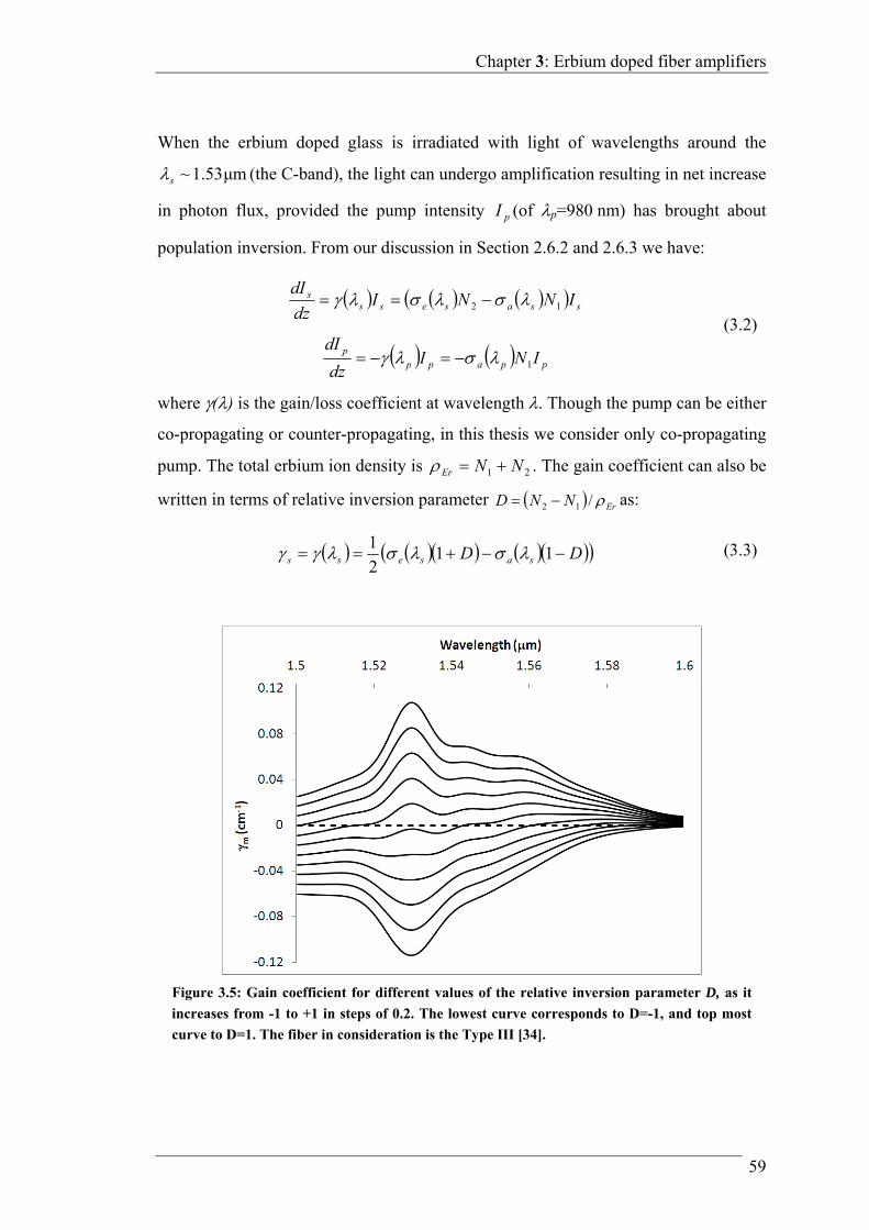
Chapter 3: Erbium doped fiber amplifiers
59
When the erbium doped glass is irradiated with light of wavelengths around the
μm53.1~s (the C-band), the light can undergo amplification resulting in net increase
in photon flux, provided the pump intensity pI (of p=980 nm) has brought about
population inversion. From our discussion in Section 2.6.2 and 2.6.3 we have:
ssasesss INNI
dz
dI12
ppappp INI
dz
dI1
(3.2)
where () is the gain/loss coefficient at wavelength . Though the pump can be either
co-propagating or counter-propagating, in this thesis we consider only co-propagating
pump. The total erbium ion density is 21 NNEr . The gain coefficient can also be
written in terms of relative inversion parameter ErNND /12 as:
DD sasess 112
1 (3.3)
Figure 3.5: Gain coefficient for different values of the relative inversion parameter D, as it
increases from -1 to +1 in steps of 0.2. The lowest curve corresponds to D=-1, and top most
curve to D=1. The fiber in consideration is the Type III [34].
Chapter 3: Erbium doped fiber amplifiers
60
It is clear from Eq. (3.3) that gain is possible only when the relative inversion
parameter satisfies ,sesasesaD Figure 3.5 shows the
variation of gain coefficient as the inversion parameter increases from its minimum
value -1 to +1 in step of 0.2.
To determine the gain coefficient we need to know the population density N1 and N2
of energy states E1 and E2 respectively in the presence of light intensity corresponding
to pump and signal wavelengths. Since erbium doped glass can amplify signals of
wavelengths lying within its gain bandwidth, we consider the presence of a large
number of signals (as would be in a WDM system). The rate equation describing the
change of population density N1 can be written as:
spk
kkke
k
kkkapppa NN
hc
IN
hc
IN
hc
I
dt
dN
2211
1 (3.4)
where sp (=10 ms) is the spontaneous emission lifetime of transition from energy
levels E2 to E1. The first term in Eqs. (3.4) corresponds to the stimulated absorption of
the pump, the second term is a sum of absorption at all signal wavelengths, the third
term represents the stimulated emission at all signal wavelength and the last term
corresponds to the spontaneous emission from E2 to E1. The index k denotes all the
simultaneously propagating signals. Under steady state condition, 01 dtdN , and
one can obtain:
Er
kk
kp
kkk
II
IN
1~~
1
~1
1 , Er
kkkp
kkp
II
IIN
1~~
1
~~
2 (3.5)
where ksatkk III ~ and psatpp III ~
are normalized intensities at signal and
pump wavelengths respectively, with saturation intensities ksatI and psatI
defined as:

Chapter 3: Erbium doped fiber amplifiers
61
kkaspksat hcI
ppasppsat hcI (3.6)
and kakek is the ratio of emission and absorption cross-section at
wavelength k . Substituting the expressions of N1 and N2 in Eqs. (3.2) the change in
intensity Ij corresponding to jth wavelength, along propagation length are obtained as:
j
kkkp
kkk
kkps
saErj I
II
III
dz
dI
1~~
1
~1
~~
(3.7)
p
kkkp
kkk
paErp I
II
I
dz
dI
1~~
1
~1
(3.8)
3.3 Power coupled equations
In an erbium doped optical fiber with n1=1.458, n2=1.45, aco=2.5 m, and acl=62.5 m
the pump and signal powers travel in well defined LP01 modes. The radial dependence
of the modal fields is given by [47,48,110]:
raa
rWK
WK
A
ara
rUJ
UJ
A
r
coco
coco
00
00
)(
)()( (3.9)
where 2/1221
20 )( nkaU co and 2/12
220
2 )( nkaW co .and is the propagation
constant. The constant A can be determined using the normalization of the modal field
as
0
2 12 rdrr as:
21
220
22
1
120
12
12
)(
)(
)(
)(2
UK
UK
UJ
UJaA co (3.10)

Chapter 3: Erbium doped fiber amplifiers
62
Figure 3.6 shows the modal fields for signal wavelength, =1.53 m and pump
wavelength, =980 nm. The intensity distribution at any wavelength j is given by
rPrI jjj2 where Pk is the total power in the fiber at k and rk is the
corresponding modal field distribution, thus equations describing the variation of
propagation power can be written as:
zPzdz
zdPjj
j (3.11)
rdrr
rPrP
rPrPrP
z j
kkk
kkp
kkkk
kkkppk
jaErj2
022
222
1~~
1
~1
~~
2
(3.12)
Similarly we have for pump power:
zPzdz
zdPpp
p (3.13)
Figure 3.6:Normalized modal field profiles corresponding at signal wavelength =1.53 m
(S) and at pump wavelength =980 nm (P), with n1=1.458, n2=1.45, aco=2.5 m and
acl=62.5 m.
Chapter 3: Erbium doped fiber amplifiers
63
rdrrzP
rPrP
rPz pp
kkkkpp
kkkk
paErp2
022
2
1~~
1
~1
2
(3.14)
and pjsatpjpj IPP ,,,
~ . The gain coefficient pj , depends on propagation distance z.
Eqs. (3.11) and (3.13) form a set of coupled differential equations; the number of
equations is determined by the number of signal wavelengths propagating
simultaneously. These equations can be solved using the Fourth order Runge-Kutta
method. If we consider 125 signals in wavelength range 1.5 < < 1.6 m, separated
by a spacing of 8 nm propagating simultaneously, we have to solve 125+1=126 couple
differential equations at equally spaced intervals along z direction.
3.3.1 Amplified spontaneous emission
The de-excitation of atoms in state E2 due to spontaneous emission adds to the signal
photons and is also amplified as it propagates through the fiber. This amplified
spontaneous emission is essentially a noise, since it is also present in the absence of
signals. The light generated by spontaneous emission has a random phase and
direction, and part of it is coupled into the propagating mode and amplified. It
emerges from both ends of the doped fiber and must be dealt with. ASE in the same
direction as the signal is a major source of cumulative noise (reducing signal to noise
ratio), while backward propagating ASEs can harm source lasers if not filtered out.
The presence of ASE also reduces the available optical gain for the signal field. Thus
it is important to include ASE, in the modeling of EDFAs. In this section we derive
the power rate equation to include ASE.
Following the analysis given by Desuvire [34] , the number of randomly polarized
photons (per unit time) in the frequency interval f and f+df that are spontaneously
generated per unit time within a small volume dV of the gain medium, and coupled
into the fiber mode is given by:
rdrrrNdzdfffdn je2
0
2 ,4
(3.15)
The energy of these spontaneously emitted photons is hf, thus the corresponding
spontaneous emission power added is given by fhfdndPSE . Hence, the
Chapter 3: Erbium doped fiber amplifiers
64
spontaneous emission power in the frequency interval f and f+df is generated in small
section dz is:
dzrdrrrNfPdP jej
SE
2
0
20)( ,4 (3.16)
where hfdfP 0 is often referred to as equivalent input noise. Using the expression for
N2 (Eq. 3.5 ), we can rewrite the above equation as:
dzrdrr
rPrP
rPrPfPdP jEr
kkkkpp
kkkpp
ej
SE
2
022
22
0)(
~1
~1
~~
4
(3.17)
This generated spontaneous power is amplified as it travels down the gain fiber and
stimulates the emission of more photons. Moreover ASE power generated can travel
either forward or backward.
The power affecting the population is now the sum of net forward and backward
propagating powers. Thus, including forward and backward propagating ASE, the
power propagation equations can be written as:
dz
dPzPz
dz
zdP jSE
jjj
)(
(3.18)
where now signal gain coefficient zj is:
rdrr
rPPrP
rPPrPPrP
z j
kkk
kkkp
kkkkk
kkkkppk
jaErj2
022
222
1~~~
1
~~1
~~~
2
(3.19)
And the pump power is:
zPzdz
zdPpp
p (3.20)
where zp is also modified to:
rdrrzP
rPPrP
rPPz pp
kkkkkpp
kkkkk
paErp2
022
2
1~~~
1
~~1
2
(3.21)
Chapter 3: Erbium doped fiber amplifiers
65
Here, jP includes the forward propagating signal and ASE, while
jP refers to the
backward propagating ASE. Thus considering the wavelength range of interest,
1.5 < < 1.6 m, and df corresponding to a wavelength spacing of 8 nm, we now
have to solve additional 125 equations for the backward propagating ASE, resulting in
total 125+125+1=251 coupled differential equations to be solved simultaneously.
The presence of backward ASE introduces a two boundary problem, which leads to
the necessity of iterative forward and backward integration. An initial set of boundary
values is chosen for the first integration from z=0 to z=L, L being the length of the
fiber, with both backward and forward ASE zero at z=0. The equations (3.18) and
(3.20), for each signal wavelength, are then integrated from z=0 to z=L. The system of
equations is then integrated again, in reverse direction from z=L to z=0, with
corrected boundary value, i.e. setting the backward ASE to zero at z=L, and other
amplitudes as obtained from the forward integral. In the next iteration, from z=0 to
z=L, the forward ASE is set to zero at z=0, all signal and pump powers are set to their
original value at z=0, and backward ASE to the value obtained. The whole process is
iterated till convergence is reached.
3.3.2 Simplified power equations
The 251 coupled differential equations, also involve integrals containing modal field
profiles for each signal wavelength, and in order to obtain the solution we need to
calculate these integrals for each wavelength at each equally spaced interval along the
length of the fiber. This is computationally extensive and consumes time. Sunanda et
al. [125] proposed the use of a rectangular approximation for the modal intensity
profile, i.e., approximated rk2 to:
ps
psps
psR
ar
ara
r
,
,2,
2),(
0
1
(3.22)
Chapter 3: Erbium doped fiber amplifiers
66
where the parameter as,p is chosen such that the overlap of the exact field and the
approximated rectangular field with the erbium ion profile are the same, i.e.:
drrrr
drrrr
psEr
psREr
ps 2,
0
2),(
0, 22
(3.23)
Thus, for a constant erbium ion profile 22, cops aa and the overlap given by:
UJUJ
UJcWVK
cWUK 21
20
2
011
10
(3.24)
where 222 WUV .
Figure 3.7 shows the rectangular modal field along with the exact modal field for our
fiber at 1.53 m (S) and 980 nm (P). Using these approximations, the pump, and
signal (including ASE) power equations are simplified to:
Figure 3.7:Nnormalized modal field profiles corresponding to Exact (dashed line) and
Rectangular Approximation (solid line)) at signal wavelength =1.53 m (S) and at pump
wavelength =980 nm (P)

Chapter 3: Erbium doped fiber amplifiers
67
zPppp
ppzP
dz
zdPp
kkkkp
kkkk
ppaErppp
11
1 (3.25)
kkkkp
kkkps
jjajjj
ppp
ppp
PzPdz
zdP
112 00 ;
kkkkp
kkkk
kkkkp
kkkps
jjaj ppp
pp
ppp
ppp
11
1
110
(3.26)
where kp and q are now the normalized signal and pump powers defined as
ksatASEkk PPPp and psatpp PPp , with the saturation signal and pump
powers defined as 2kksatksat aIP and 2
ppsatpsat aIP .
Table 3-2: Parameters used for modeling the EDF
Symbol Parameter Value
n1 Core index 1.458
n2 Clad index 1.450
aco Core radius 2.5 m
acl Clad radius 62.5 m
0 Erbium ion density 1.62x1025 m-3
L Length of the fiber 4 m
These equations can be used to obtain the gain and ASE noise characteristics of an
EDF. The typical EDF parameters used for simulation in this chapter are listed in
Table 3-2. Figure 3.8 shows the gain at wavelength =1.53 m as a function of pump
power at 980 nm for a 4 m long EDF for both cases: (i) when the presence of ASE is
taken into account, (ii) when ASE is neglected. It shows that gain increases with pump
power, but at high pump powers, when the relative inversion level is strong, the gain
is saturated. The gain saturates because when all erbium ions are excited, i.e., full
inversion is reached, then the gain is maximum, after that any further increase in pump
power will have no affect on inversion and thus gain. Also, the presence of ASE can
significantly lowers the gain, especially at low signal power levels. Figure 3.9 shows

Chapter 3: Erbium doped fiber amplifiers
68
the gain spectrum when 125 signals in the wavelength range 1.5 m to 1.6 m are co
propagating. The gain is non uniform with a gain excursion of more than 20 dB across
the 40 nm useful bandwidth of 1.52 m to 1.56 m.
Figure 3.8: Signal gain for=1.53 m propagating through the a typical 4m EDF as the
pump power (980 nm) is varied. Dashed curves correspond when ASE is not considered in
calculations. Solid curves correspond when ASE is considered for calculations.
Figure 3.9: Gain spectrum of a typical EDF when 125 signals in wavelength range 1.5 to
1.6 m with a power of 100 nW each, is launched in the 4m long EDF.
Chapter 3: Erbium doped fiber amplifiers
69
Since at low signal powers ASE plays more significant effect, we first considered
ASE in 4 m EDF when no input signal was present. Figure 3.10 and Figure 3.11 show
the forward and backward ASE spectrum, in the absence of any input signal. As
expected, with increase in pump power more inversion is created leading to higher
ASE power. Since we have considered a co-propagating pump, the backward ASE is
more than the forward ASE. The reason for backward ASE being slightly more than
Figure 3.10: Forward ASE spectrum of a typical EDF in the absence of any input signal.
Figure 3.11: Backward ASE spectrum of a typical EDF in the absence of any input signal.

Chapter 3: Erbium doped fiber amplifiers
70
the forward ASE for a co-propagating pump is that, at the starting of EDF, the pump is
higher leading to high inversion level and thus more amplification and generation of
spontaneous emission.
3.4 Erbium doped fiber amplifier with long period grating
written in it
Figure 3.9 shows that the gain spectrum of the EDF, as can be seen,. gain is not same
for all signal wavelengths. This is a problem for WDM systems, as it can result in
signal distortion. Various techniques have been proposed to flatten the gain spectrum.
The techniques involve can be either intrinsic or extrinsic. One of the popular extrinsic
technique for gain flattening is the use of an external optical gain flattening filter
(GFF) having a loss profile that is reverse of the gain spectra of EDF. Various types of
optical GFFs have been proposed using dielectric filters, twin core fiber filter [79],
long and short period fiber gratings [107,51,143] and acousto-optic tunable filters [71]
etc.
More recently, Singh et al. [119] proposed an alternative technique of gain flattening
by use of an appropriately chosen long period grating written through a length of EDF
itself. The grating was chosen so as to, couple the wavelength experiencing peak gain
into the cladding, thus inversion in core is made available to other wavelengths. As a
result, in this configuration, there was gain flattening as well as increase in the average
gain across the 1.54 m -1.56 m band. To study the characteristics of such a 980 nm
pumped EDF with a grating written in it, they reformulated the conventional coupled
mode analysis of the long period grating to include the EDF gain term (Appendix B).
However, the reformulated analysis did not account for the presence of spontaneous
emission and the effect of the LPG on ASE noise in EDF. A LPG is a phase sensitive
device and hence to add the spontaneous emissions generated in each section of the
EDF it is necessary to account for both its amplitude and phase.
3.4.1 Amplified spontaneous emission in phase sensitive structures
In a conventional EDF (i.e., without a LPG), generation and amplification of
spontaneous emission can be studied using coupled equations in terms of power
Chapter 3: Erbium doped fiber amplifiers
71
(Section 3.3.1). However, because LPG is a phase sensitive device, it is necessary to
consider both the amplitude and phase of the propagating signals. Hence, in order to
estimate ASE for a 980 nm pumped EDF with LPG written in it, we have
reformulated the conventional coupled mode analysis to include the EDF gain as well
as the ASE. To include ASE, we have to add the generated spontaneous emission
amplitude with a random phase at each section of the EDF. In order to validate this
approach, we have compared the results obtained for the EDF in absence of LPG
using our approach with those obtained by the standard power coupled equations. Our
results show reasonable matching between two.
From the discussion in Section 3.3.1 we know the increase in the power due to
spontaneous emission in a small length dz of fiber, we can rewrite it as:
dzNPdzrdrrrNfPdP SEseSE 02
0
20 2,4
(3.27)
where we define NSEdz as the number of spontaneously emitted photons in small fiber
length dz, and hfdfP 0 is the power of one spontaneous photon in the frequency
interval f and f+df. The factor of 2 in above equation represents the fact that
spontaneous emission occurs in both polarization modes of the fiber. Alternatively, we
can view each spontaneous emission as a field with constant amplitude 0P and a
random phase , lying between 0 and 2 . A single spontaneous emission into one
mode can be thus written as:
ieP0 (3.28)
And the number of randomly polarized photons in the frequency interval f and f+df
that are spontaneously generated within a small volume dV of the gain medium, and
coupled into the fiber mode are given as:
rdrrrNdzfN seSE2
0
2 ,2
(3.29)
Applying rectangular approximation, we get:
Chapter 3: Erbium doped fiber amplifiers
72
dzpp
ppf
N
kkkp
kkpeos
SE
11
)(
(3.30)
Thus the net amplitude of all the spontaneous emission, emitted in the small fiber
length dz, coupling into the fiber mode will be sum of all such spontaneous emissions:
SE
i
N
i
iSE ePfdA
10
(3.31)
The term on the RHS of above equation, is a complex number, it is possible to express
it as:
iSESESE eNPibaNPfdA 00 )( (3.32)
where ab /tan 1 will be a random number lying between 0 and , and
122 ba . Using equation (3.30) we get:
dzpp
ppf
ePfdA
kkkp
kkpeos
SE
11
)(
0 (3.33)
The ASE so generated is both co-directional and counter-directional to the signal,
referred as forward and backward ASE respectively. Hence, in order to accommodate
ASE in the coupled mode analysis we will have to consider both forward and
backward propagating fields. Thus, we incorporate this in the modified amplitude
coupled Eqs. (ACE) yielding:
dz
dAAz
zi
BKze
zi
Azzz
dz
Ad
ASEj
jjjjjj
jj
jzi
jjj
jjjjjjj
j
~
2
~)sin(4
2
~122
~
''
1
)(121
'1
''1
22'
(3.34)
)(2
)sin(4
)(2 2
)(212
2
2
j
jj
jzi
j
jj
i
AKze
i
B
dz
Bd j
(3.35)
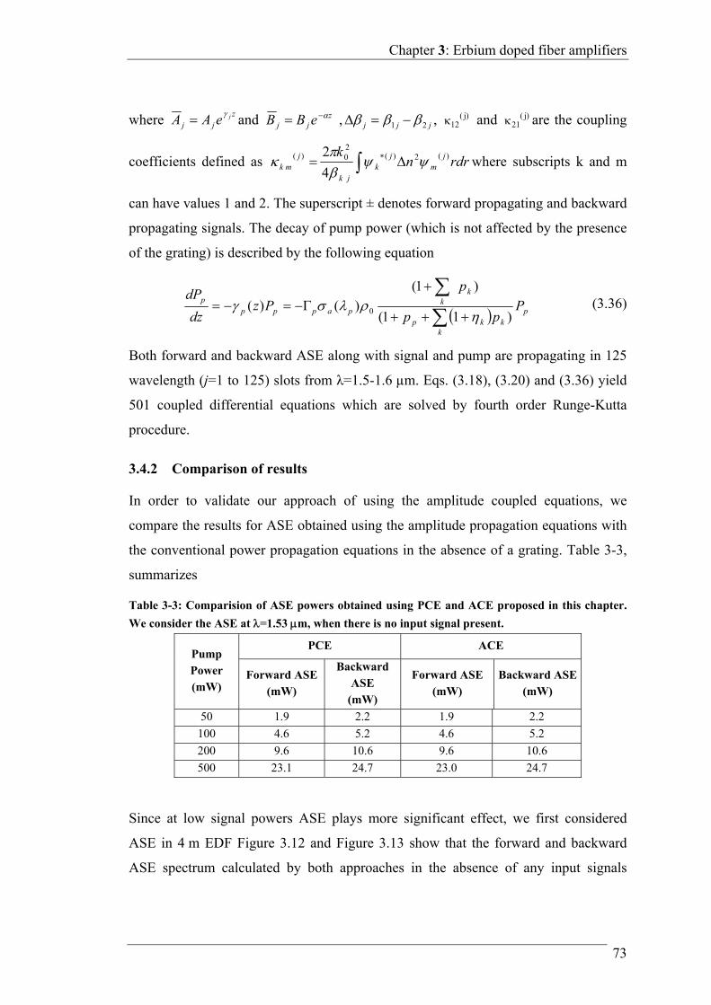
Chapter 3: Erbium doped fiber amplifiers
73
where zjj
jeAA and zjj eBB , jjj 21 , )j(
12 and )j(21 are the coupling
coefficients defined as rdrnk j
mj
kjk
jmk
)(2)(20)(
4
2
where subscripts k and m
can have values 1 and 2. The superscript ± denotes forward propagating and backward
propagating signals. The decay of pump power (which is not affected by the presence
of the grating) is described by the following equation
p
kkkp
kk
papppp P
pp
pPz
dz
dP
)11(
)1()()( 0
(3.36)
Both forward and backward ASE along with signal and pump are propagating in 125
wavelength (j=1 to 125) slots from λ=1.5-1.6 µm. Eqs. (3.18), (3.20) and (3.36) yield
501 coupled differential equations which are solved by fourth order Runge-Kutta
procedure.
3.4.2 Comparison of results
In order to validate our approach of using the amplitude coupled equations, we
compare the results for ASE obtained using the amplitude propagation equations with
the conventional power propagation equations in the absence of a grating. Table 3-3,
summarizes
Table 3-3: Comparision of ASE powers obtained using PCE and ACE proposed in this chapter.
We consider the ASE at =1.53 m, when there is no input signal present.
Pump Power (mW)
PCE ACE
Forward ASE (mW)
Backward ASE
(mW)
Forward ASE (mW)
Backward ASE (mW)
50 1.9 2.2 1.9 2.2
100 4.6 5.2 4.6 5.2
200 9.6 10.6 9.6 10.6
500 23.1 24.7 23.0 24.7
Since at low signal powers ASE plays more significant effect, we first considered
ASE in 4 m EDF Figure 3.12 and Figure 3.13 show that the forward and backward
ASE spectrum calculated by both approaches in the absence of any input signals
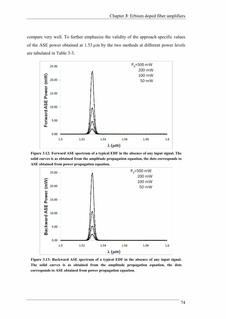
Chapter 3: Erbium doped fiber amplifiers
74
compare very well. To further emphasize the validity of the approach specific values
of the ASE power obtained at 1.53 m by the two methods at different power levels
are tabulated in Table 3-3.
Figure 3.12: Forward ASE spectrum of a typical EDF in the absence of any input signal. The
solid curves is as obtained from the amplitude propagation equation, the dots corresponds to
ASE obtained from power propagation equation.
Figure 3.13: Backward ASE spectrum of a typical EDF in the absence of any input signal.
The solid curves is as obtained from the amplitude propagation equation, the dots
corresponds to ASE obtained from power propagation equation.
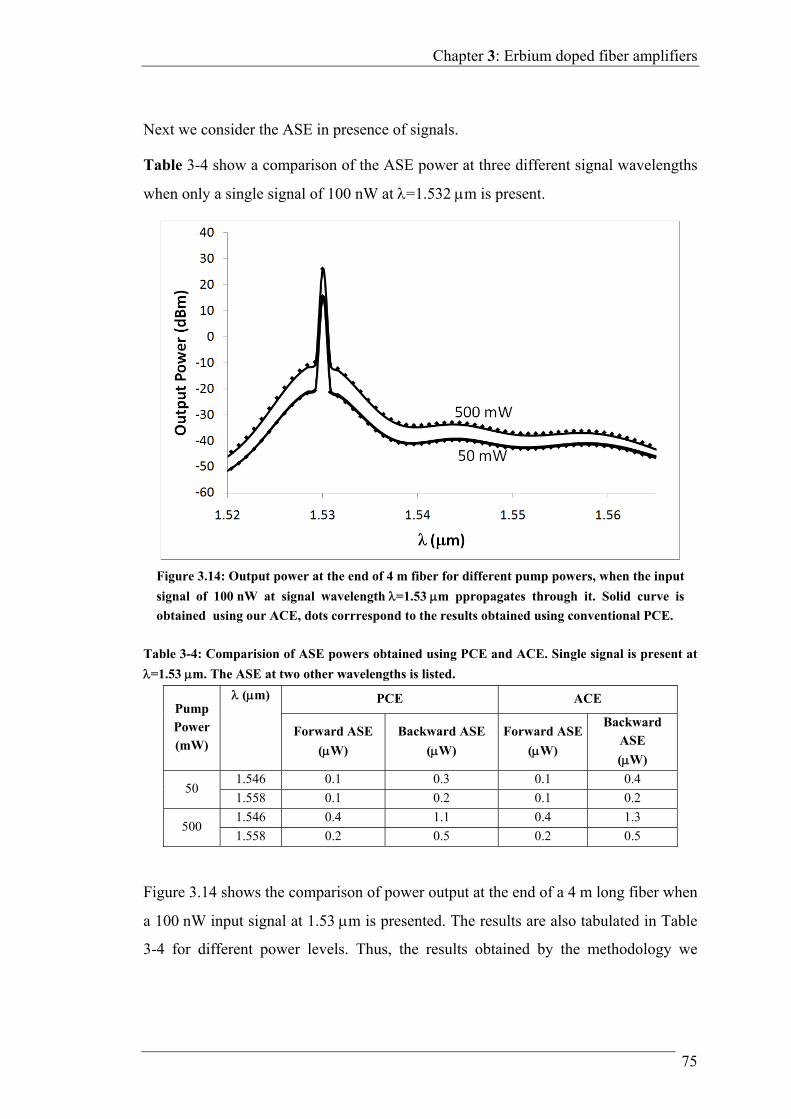
Chapter 3: Erbium doped fiber amplifiers
75
Next we consider the ASE in presence of signals.
Table 3-4 show a comparison of the ASE power at three different signal wavelengths
when only a single signal of 100 nW at =1.532 m is present.
Table 3-4: Comparision of ASE powers obtained using PCE and ACE. Single signal is present at
=1.53 m. The ASE at two other wavelengths is listed.
Pump Power (mW)
(m) PCE ACE
Forward ASE
(W)
Backward ASE
(W)
Forward ASE
(W)
Backward ASE
(W)
50 1.546 0.1 0.3 0.1 0.4
1.558 0.1 0.2 0.1 0.2
500 1.546 0.4 1.1 0.4 1.3
1.558 0.2 0.5 0.2 0.5
Figure 3.14 shows the comparison of power output at the end of a 4 m long fiber when
a 100 nW input signal at 1.53 m is presented. The results are also tabulated in Table
3-4 for different power levels. Thus, the results obtained by the methodology we
Figure 3.14: Output power at the end of 4 m fiber for different pump powers, when the input
signal of 100 nW at signal wavelength=1.53 m ppropagates through it. Solid curve is
obtained using our ACE, dots corrrespond to the results obtained using conventional PCE.

Chapter 3: Erbium doped fiber amplifiers
76
propose to include ASE shows good agreement with the conventional power
propagation approach used to model ASE both in presence and absence of signal.
3.5 ASE suppression in EDF with LPG written in it
Our main interest in developing the proposed method to include ASE was to
investigate the effect of LPG written in EDF on the ASE noise. Using the method
evolved, we investigated the effect of LPG written in EDF itself on the ASE. Table
3-5 lists the parameter of the grating written in EDF for our calculations. The grating
period of 267 m corresponds to a mode coupling between LP01-LP09 modes at a
signal wavelength of 1.53 m (Figure 2.13). The LP01-LP09 mode coupling was
chosen since it provides attenuation over the desired bandwidth.
Table 3-5 Grating parameters
Symbol Parameter Value
2n Refractive index modulation 2x10⁻⁴
Grating period 267 m
l Length of grating 340 cm
Figure 3.15: Gain spectrum of the EDF, when 125 signals of 100 nW each are launched in the
fiber. Solid curve: EDF with LPG written in it. Dashed curve: EDF without LPG. Pump
power: 500 mW
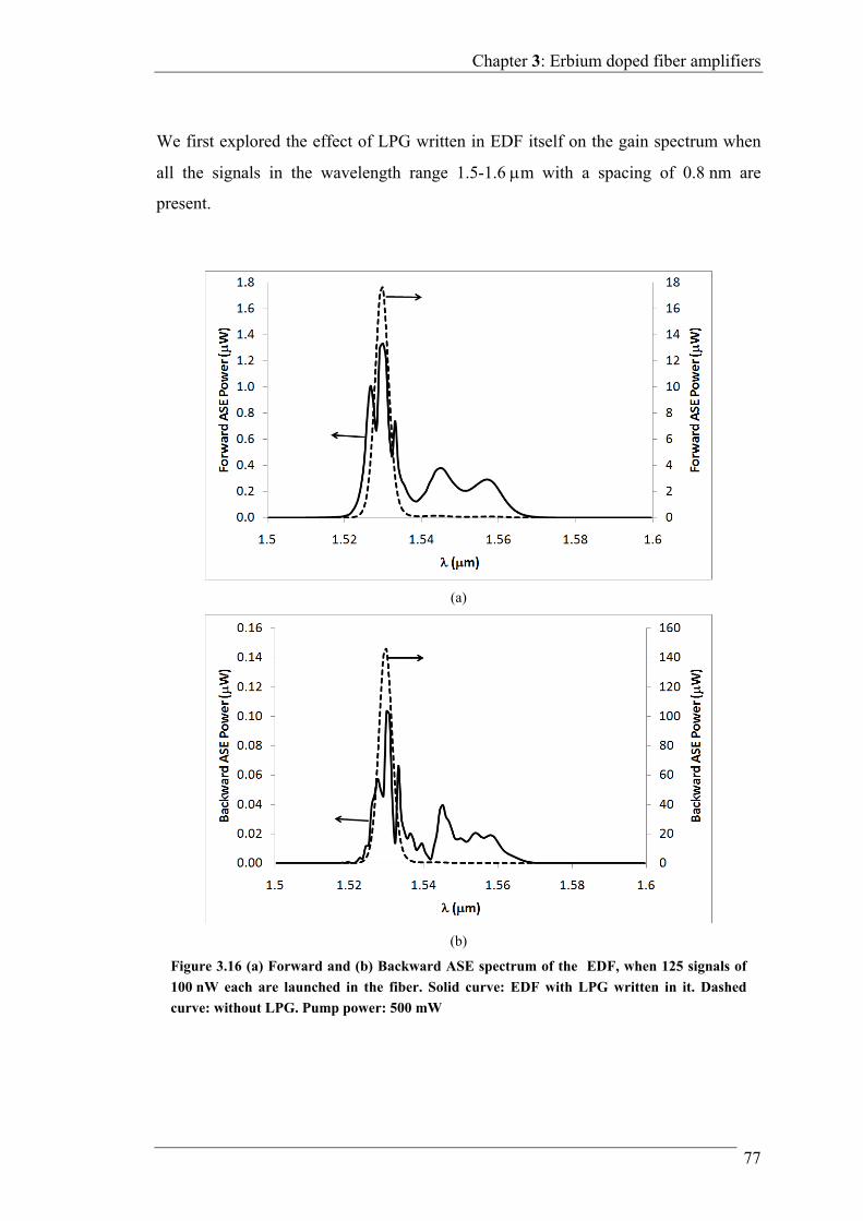
Chapter 3: Erbium doped fiber amplifiers
77
We first explored the effect of LPG written in EDF itself on the gain spectrum when
all the signals in the wavelength range 1.5-1.6 m with a spacing of 0.8 nm are
present.
(a)
(b)
Figure 3.16 (a) Forward and (b) Backward ASE spectrum of the EDF, when 125 signals of
100 nW each are launched in the fiber. Solid curve: EDF with LPG written in it. Dashed
curve: without LPG. Pump power: 500 mW
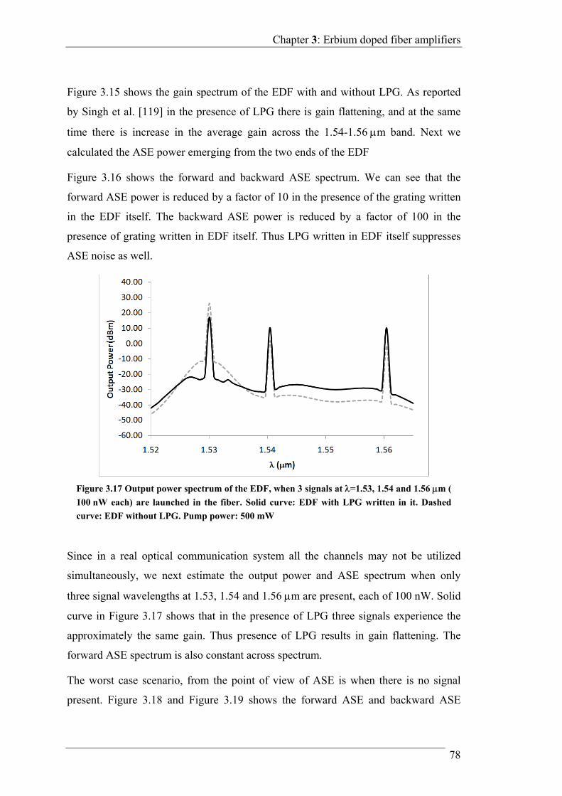
Chapter 3: Erbium doped fiber amplifiers
78
Figure 3.15 shows the gain spectrum of the EDF with and without LPG. As reported
by Singh et al. [119] in the presence of LPG there is gain flattening, and at the same
time there is increase in the average gain across the 1.54-1.56 m band. Next we
calculated the ASE power emerging from the two ends of the EDF
Figure 3.16 shows the forward and backward ASE spectrum. We can see that the
forward ASE power is reduced by a factor of 10 in the presence of the grating written
in the EDF itself. The backward ASE power is reduced by a factor of 100 in the
presence of grating written in EDF itself. Thus LPG written in EDF itself suppresses
ASE noise as well.
Since in a real optical communication system all the channels may not be utilized
simultaneously, we next estimate the output power and ASE spectrum when only
three signal wavelengths at 1.53, 1.54 and 1.56 m are present, each of 100 nW. Solid
curve in Figure 3.17 shows that in the presence of LPG three signals experience the
approximately the same gain. Thus presence of LPG results in gain flattening. The
forward ASE spectrum is also constant across spectrum.
The worst case scenario, from the point of view of ASE is when there is no signal
present. Figure 3.18 and Figure 3.19 shows the forward ASE and backward ASE
Figure 3.17 Output power spectrum of the EDF, when 3 signals at =1.53, 1.54 and 1.56 m (
100 nW each) are launched in the fiber. Solid curve: EDF with LPG written in it. Dashed
curve: EDF without LPG. Pump power: 500 mW
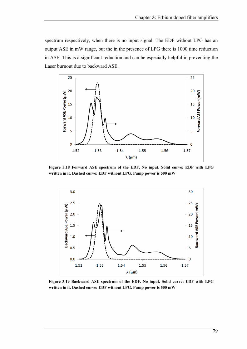
Chapter 3: Erbium doped fiber amplifiers
79
spectrum respectively, when there is no input signal. The EDF without LPG has an
output ASE in mW range, but the in the presence of LPG there is 1000 time reduction
in ASE. This is a significant reduction and can be especially helpful in preventing the
Laser burnout due to backward ASE.
Figure 3.18 Forward ASE spectrum of the EDF. No input. Solid curve: EDF with LPG
written in it. Dashed curve: EDF without LPG. Pump power is 500 mW
Figure 3.19 Backward ASE spectrum of the EDF. No input. Solid curve: EDF with LPG
written in it. Dashed curve: EDF without LPG. Pump power is 500 mW
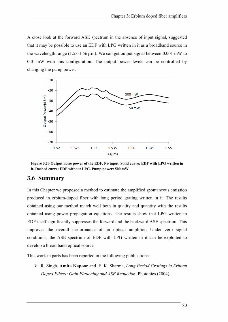
Chapter 3: Erbium doped fiber amplifiers
80
A close look at the forward ASE spectrum in the absence of input signal, suggested
that it may be possible to use an EDF with LPG written in it as a broadband source in
the wavelength range (1.53-1.56 m). We can get output signal between 0.001 mW to
0.01 mW with this configuration. The output power levels can be controlled by
changing the pump power.
3.6 Summary
In this Chapter we proposed a method to estimate the amplified spontaneous emission
produced in erbium-doped fiber with long period grating written in it. The results
obtained using our method match well both in quality and quantity with the results
obtained using power propagation equations. The results show that LPG written in
EDF itself significantly suppresses the forward and the backward ASE spectrum. This
improves the overall performance of an optical amplifier. Under zero signal
conditions, the ASE spectrum of EDF with LPG written in it can be exploited to
develop a broad band optical source.
This work in parts has been reported in the following publications:
R. Singh, Amita Kapoor and .E. K. Sharma, Long Period Gratings in Erbium
Doped Fibers: Gain Flattening and ASE Reduction, Photonics (2004).
Figure 3.20 Output noise power of the EDF. No input. Solid curve: EDF with LPG written in
it. Dashed curve: EDF without LPG. Pump power: 500 mW
Chapter 3: Erbium doped fiber amplifiers
81
Amita Kapoor, R. Singh, E. K. Sharma, Study of ASE in LPG written in
amplifying EDF: A Novel Analytical Approach, , MATEIT, Deen Dayal
Upadhyaya College, Delhi, India, 22-25th March (2006).
Amita Kapoor, R. Singh and E. K. Sharma, Estimation of Amplified
Spontaneous Emission in Erbium Doped Fiber with Long Period Grating
Written in it, The Second Research Forum of Japan-Indo Collaboration Project
on Infrastructural Communication Technologies Supporting Fully Ubiquitous
Information Society, Kyushu University, Fukuoka, Japan, Forum Digest, pp
57-61, (2007).
Amita Kapoor, R. Singh and E. K. Sharma, Suppression of Amplified
Spontaneous Emission in Erbium Doped Fiber with Long Period Grating
written in it, Proc. Asia Pacific Microwave Conference, pp 2631-4, (2007).

Chapter 4: Erbium doped lithium niobate waveguide amplifiers
83
4 Erbium doped lithium niobate waveguide amplifiers
4.1 Introduction
The advent of metropolitan and access optical networks has brought optical systems
nearer to the end user. A direct consequence of this is the increase in the demand of
compact integrated optical components. Titanium indiffused channel waveguides in
LiNbO3 (lithium niobate) have been as the backbone of integrated optical components
because lithium niobate has excellent electro-optical, acousto-optical and nonlinear
optical properties making it the choicest material for electro-optical modulators,
acousto-optically tunable wavelength filters and Bragg gratings. Doping LiNbO3
waveguides with erbium ions, under proper pumping conditions forms an amplifying
medium for wavelengths around 1.53 m. This makes integrated erbium doped
waveguide amplifiers (EDWA) and erbium laser oscillators possible. The
amplification can also compensate for absorption, connection and background losses,
making erbium doped LiNbO3 waveguides an useful component in lossless (“zero
loss”) passive components.
Reduced size, bidirectional operation [33], and insensitivity to burst transmission
[127] makes EDWAs a low cost alternative to EDFAs in metropolitan optical
Chapter 4: Erbium doped lithium niobate waveguide amplifiers
84
networks [99]. In order to optimize the performance of Er-doped diffused channel
waveguide amplifiers the analysis of gain and noise characteristics of EDWAs is
required. Similar to the erbium doped fiber amplifier, the amplifying erbium ions are
now hosted in a diffused channel waveguide and the gain characteristics will depend
on the modal fields of the waveguide. However, as mentioned in Chapter 2, the modal
fields for a diffused channel waveguide cannot be solved analytically. Various
numerical and approximate methods are used instead to solve for the modal fields.
One such method, the variational method was discussed briefly in Chapter 2 which
provides an analytical form for the modal field profile. However, in spite of using this
analytical form of the modal fields, the coupled differential equations for power
evolution in the amplifying waveguide, still contain integrals which cannot be solved
analytically. In this Chapter, we present approximations for the modal fields, which
reduce these integrals to analytical form, while maintaining the accuracy. The
corresponding simplified calculations of gain and noise characteristics are also
presented in this Chapter.
4.2 Erbium in lithium niobate
We have already discussed in Section 3.2, the energy levels and emission/absorption
properties of erbium ions in a silica host glass. These are modified by the host
material. In this section we study how the LiNbO3 host modifies the energy structure
of erbium ions. Figure 4.1 shows the complete energy level diagram of erbium ions in
LiNbO3 host, as measured by Gabrielyan et al [46]. When erbium is doped in LiNbO3
lattice, Er3+ ions replace the Li+ ions. The electric field of adjacent atoms result in the
splitting of the ground state 4I15/2 into 8 doubly degenerate levels and the first excited
state 4I13/2 into 7 Stark sublevels. Transition between both manifolds determines the
optical absorption and emission in the wavelength range 1.44 µm ≤ λ ≤ 1.64 µm. Both,
980 nm and 1484 nm pump wavelengths are possible. However, excited state
absorption (ESA) is weak for 1484 nm [13], hence it is the preferred pump for
Er:LiNbO3. In addition, for λp=1484 nm, the fabricated optical waveguides are single
moded for both pump and signal wavelength; this results in a good field overlap.
Chapter 4: Erbium doped lithium niobate waveguide amplifiers
85
For our illustrative calculations we use the erbium doped titanium indiffused LiNbO3
amplifying waveguide, characterized both theoretically and experimentally by Dinand
and Sohler [39]. The waveguide was fabricated by the indiffusion of a 7 mm wide,
and 95 nm thick Ti-stripe.in Z-cut LiNbO3. at diffusion temperature of 1030 ºC for
9 h. this results in a waveguide (which was also discussed in Chapter 2) with a
refractive index profile ),( yxn represented as:
0airfor1
02,2
22 2222
yn
yeennnyxn
c
hywxss (4.1)
The fabricated waveguide parameters are ns = 2.297, n = 0.0048, w = 7.5 µm and
h = 6.5 µm [39]. The erbium ion profile (Figure 4.2) is Gaussian:
erEr hyy 220 exp)( (4.2)
with her=5.12 m, and 0 = 6.6x1025 m-3 is assumed which corresponds to the
indiffusion of an erbium layer at 1100 ºC for 100 h:
Figure 4.1: Energy level diagram of erbium ions in lithium niobate host, taken from
Gabrielyan et al [46].
Chapter 4: Erbium doped lithium niobate waveguide amplifiers
86
The absorption ( )( ka ) and emission ( )( ke ) cross-sections of erbium in LiNbO3
differ significantly from those in silica host as shown in Figure 4.3, the cross-sections
have been reproduced from the results reported by Dinand and Sohler [39].
Figure 4.2: The typical Gaussian erbium ion profile
Figure 4.3: Absorption and emission cross sections of Er:LiNbO3
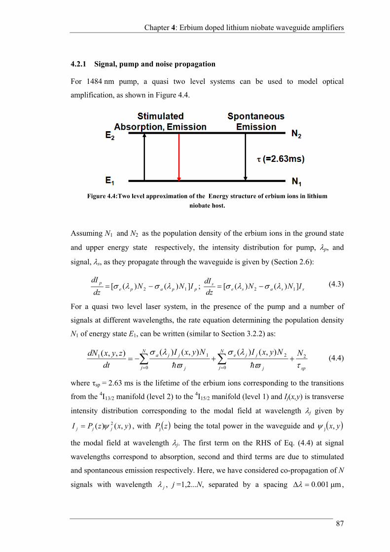
Chapter 4: Erbium doped lithium niobate waveguide amplifiers
87
4.2.1 Signal, pump and noise propagation
For 1484 nm pump, a quasi two level systems can be used to model optical
amplification, as shown in Figure 4.4.
Assuming N1 and N2 as the population density of the erbium ions in the ground state
and upper energy state respectively, the intensity distribution for pump, p, and
signal, s, as they propagate through the waveguide is given by (Section 2.6):
ppapep INN
dz
dI])()([ 12 ; ssase
s INNdz
dI])()([ 12 (4.3)
For a quasi two level laser system, in the presence of the pump and a number of
signals at different wavelengths, the rate equation determining the population density
N1 of energy state E1, can be written (similar to Section 3.2.2) as:
sp
N
j j
jjeN
j j
jja NNyxINyxI
dt
zyxdN
2
0
2
0
11),()(),()(),,(
(4.4)
where τsp = 2.63 ms is the lifetime of the erbium ions corresponding to the transitions
from the 4I13/2 manifold (level 2) to the 4I15/2 manifold (level 1) and Ij(x,y) is transverse
intensity distribution corresponding to the modal field at wavelength j given by
),()( 2 yxzPI jjj , with zPj being the total power in the waveguide and yx,j
the modal field at wavelength j. The first term on the RHS of Eq. (4.4) at signal
wavelengths correspond to absorption, second and third terms are due to stimulated
and spontaneous emission respectively. Here, we have considered co-propagation of N
signals with wavelength j , j =1,2...N, separated by a spacing μm001.0 ,
Figure 4.4:Two level approximation of the Energy structure of erbium ions in lithium
niobate host.
Chapter 4: Erbium doped lithium niobate waveguide amplifiers
88
starting with 1.485 m till 1.6 µm, j=0 corresponds to the pump wavelength
μm484.10 . It is assumed that there are no excited state absorptions (ESA) at any
of the pump and signal wavelengths [13]. Using steady state condition 01 dtdN we
obtain:
)(
,~1)(1
,~)(1
0
2
0
2
1 yyxp
yxp
NN
jjjj
N
jjjj
,
)(
,~1)(1
,~1
0
2
0
2
2 yyxp
yxp
NN
jjjj
N
jjj
(4.5)
where 21)( NNyEr is the erbium ion density, )(/)()( jajej , jp~ , is
the power at λj, normalized to its respective saturation intensity, i.e.
0))((~jjASEjj IPzPp and spjajj hcI )(0 . Using the expression for N1
and N2 the variation of intensity of signal and pump beam as they traverse through the
doped waveguide is given by
kN
jjjj
N
jjjjk
Erkak I
yxp
yxp
ydz
dI
0
2
0
2
),(~)1(1
1),(~)(
)()(
(4.6)
The total propagating power at wavelength, k, can be obtained by integrating over the
entire cross section and assuming the normalization of modal fields
0
2 1),( dydxyxk , one obtains:
kkk Pz
dz
dP)(
with
dxdyyxp
yxp
yxyzN
jjjj
N
jjjjk
kErkak
0
2
0
2
0
2
,~11
1),(~)(
),()()()(
(4.7)
As already discussed in Sections 2.6 and 3.3.1 noise due to amplification of
spontaneous emission is an inherent part of optical amplification. At each small
section dz of the amplifier, spontaneous emission is generated; it is amplified as it
Chapter 4: Erbium doped lithium niobate waveguide amplifiers
89
travels down the waveguide. Thus propagation of ASE power along the waveguide
can be given by:
dxdy
yxp
yxp
yxy
PzPdz
dP
N
jjjj
N
jjj
kEr
kekkkASEkASE
0
0
2
0
2
2
0
,~11
),(~
),()(
2)()()(
(4.8)
where lASEP refers to the ASE power for wavelength k , P0k = hfk df is the power
of one spontaneous noise photon in bandwidth df, the term is often referred in
literature as equivalent noise input. Signs refer to forward and backward
propagating ASE respectively. In Eq. (4.8) the second term denotes the ASE
generated in the section dz, and first term is due to gain of existing ASE obtained from
the previous sections.
For gain calculations in the entire wavelength range at spacing of 1 nm we have to
solve (116+2x116+1) = 349 coupled differential equations at equally spaced intervals
along z direction. These equations involve integrals containing modal fields which
have to be solved numerically at each step. Moreover for the ASE analysis, as
explained in Section 3.3.1, the whole process needs to be iterated in forward and
backward direction till we reach convergence. Thus the complete process simulation
consumes a lot of computation time.
4.2.2 Three variable variational fields
In Chapter 2, we discussed the following three parameter variational field which well
describes the model field of the titanium diffused channel waveguide [60]:
)()(),( yYxXyx (4.9)
with
2
22
1exp1
w
xa
wdxX
x
(4.10)
and
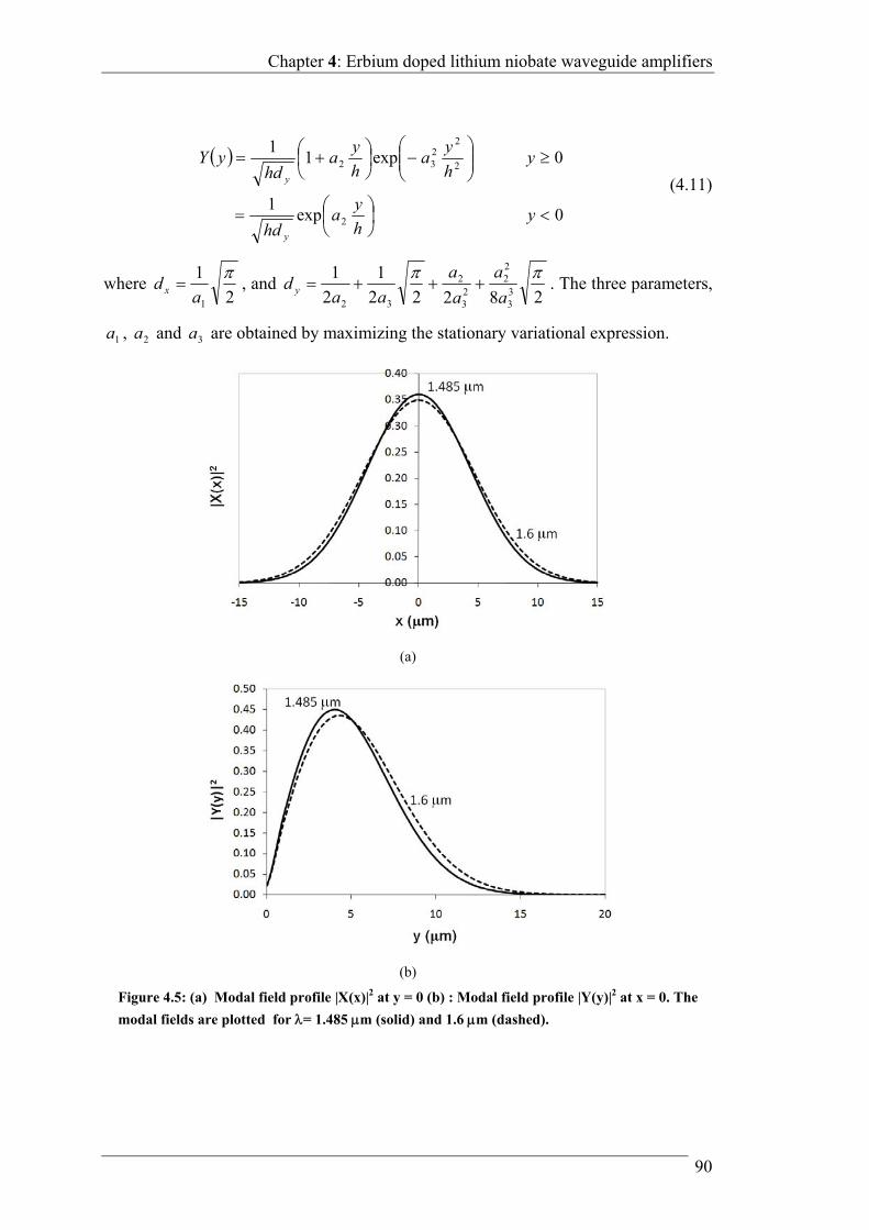
Chapter 4: Erbium doped lithium niobate waveguide amplifiers
90
0exp1
0exp11
2
2
2232
yh
ya
hd
yh
ya
h
ya
hdyY
y
y (4.11)
where 2
1
1
a
d x , and 28222
1
2
133
22
23
2
32
a
a
a
a
aad y . The three parameters,
1a , 2a and 3a are obtained by maximizing the stationary variational expression.
(a)
(b)
Figure 4.5: (a) Modal field profile |X(x)|2 at y = 0 (b) : Modal field profile |Y(y)|2 at x = 0. The
modal fields are plotted for = 1.485 m (solid) and 1.6 m (dashed).
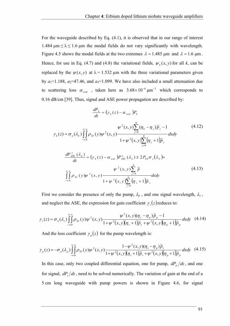
Chapter 4: Erbium doped lithium niobate waveguide amplifiers
91
For the waveguide described by Eq. (4.1), it is observed that in our range of interest
1.484 µm ≤ λ ≤ 1.6 µm the modal fields do not vary significantly with wavelength.
Figure 4.5 shows the modal fields at the two extremes μm485.1 and μm6.1 .
Hence, for use in Eq. (4.7) and (4.8) the variational fields, ),( yxk for all k, can be
replaced by the ),( yx at λ = 1.532 µm with the three variational parameters given
by a1=1.188, a2=47.46, and a3=1.099. We have also included a small attenuation due
to scattering loss scat , taken here as 16 μm1068.3 which corresponds to
0.16 dB/cm [39]. Thus, signal and ASE power propagation are described by:
kscatkk Pz
dz
dP )(
dxdy
pyx
pyx
yxyzN
jjj
N
jjjk
Erkak
0
2
0
2
0
2
~1,1
1~)(),(
),()()()(
(4.12)
dxdy
pyx
pyx
yxy
PPzdz
dP
N
jjj
N
jEr
kekkASEscatkkASE
0
0
2
0
2
2
0
~1,1
~),(
),()(
2)()()(
(4.13)
First we consider the presence of only the pump, p , and one signal wavelength, s ,
and neglect the ASE, the expression for gain coefficient zs reduces to:
dxdypyxpyx
pyxyxyz
ppss
ppsErsas ~1,~1,1
1~))(,(),()()()(
22
2
0
2
(4.14)
And the loss coefficient zp for the pump wavelength is:
dxdypyxpyx
pyxyxyz
ppss
spsErpap ~1,~1,1
~))(,(1),()()()(
22
2
0
2
(4.15)
In this case, only two coupled differential equation, one for pump, dzdPp , and one
for signal, dzdPs , need to be solved numerically. The variation of gain at the end of a
5 cm long waveguide with pump powers is shown in Figure 4.6, for signal
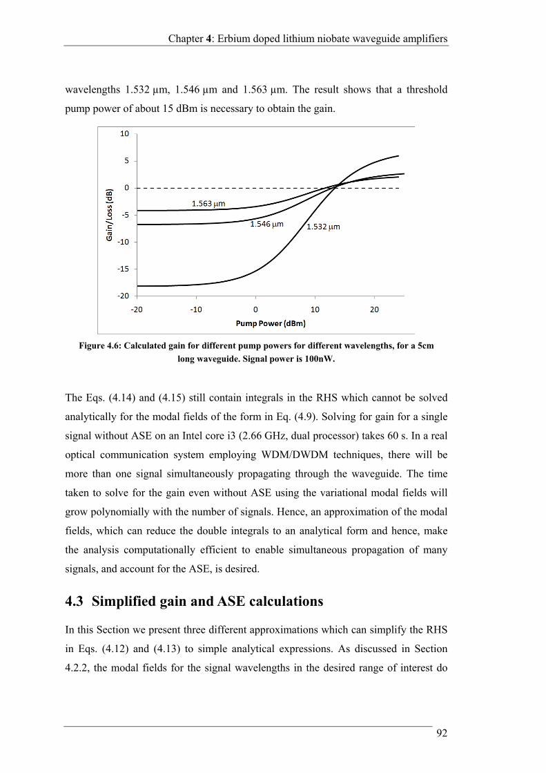
Chapter 4: Erbium doped lithium niobate waveguide amplifiers
92
wavelengths 1.532 µm, 1.546 µm and 1.563 µm. The result shows that a threshold
pump power of about 15 dBm is necessary to obtain the gain.
The Eqs. (4.14) and (4.15) still contain integrals in the RHS which cannot be solved
analytically for the modal fields of the form in Eq. (4.9). Solving for gain for a single
signal without ASE on an Intel core i3 (2.66 GHz, dual processor) takes 60 s. In a real
optical communication system employing WDM/DWDM techniques, there will be
more than one signal simultaneously propagating through the waveguide. The time
taken to solve for the gain even without ASE using the variational modal fields will
grow polynomially with the number of signals. Hence, an approximation of the modal
fields, which can reduce the double integrals to an analytical form and hence, make
the analysis computationally efficient to enable simultaneous propagation of many
signals, and account for the ASE, is desired.
4.3 Simplified gain and ASE calculations
In this Section we present three different approximations which can simplify the RHS
in Eqs. (4.12) and (4.13) to simple analytical expressions. As discussed in Section
4.2.2, the modal fields for the signal wavelengths in the desired range of interest do
Figure 4.6: Calculated gain for different pump powers for different wavelengths, for a 5cm
long waveguide. Signal power is 100nW.
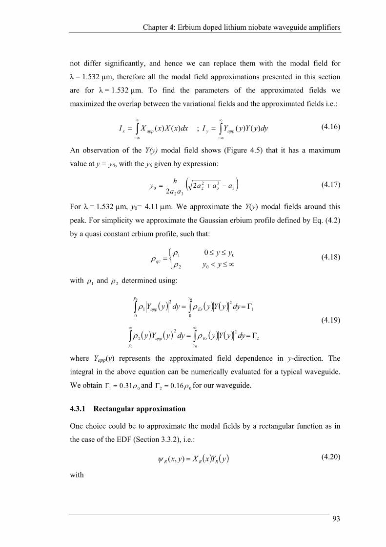
Chapter 4: Erbium doped lithium niobate waveguide amplifiers
93
not differ significantly, and hence we can replace them with the modal field for
λ = 1.532 µm, therefore all the modal field approximations presented in this section
are for λ = 1.532 µm. To find the parameters of the approximated fields we
maximized the overlap between the variational fields and the approximated fields i.e.:
dxxXxXI appx )()( ;
dyyYyYI appy )()( (4.16)
An observation of the Y(y) modal field shows (Figure 4.5) that it has a maximum
value at y = y0, with the y0 given by expression:
333
22
320 2
2aaa
aa
hy (4.17)
For λ = 1.532 µm, y0= 4.11 m. We approximate the Y(y) modal fields around this
peak. For simplicity we approximate the Gaussian erbium profile defined by Eq. (4.2)
by a quasi constant erbium profile, such that:
yy
yyqc
02
01 0
(4.18)
with 1 and 2 determined using:
1
0
2
0
2
1
00
y
Er
y
app dyyYydyyY
2
22
2
00
y
Er
y
app dyyYydyyYy
(4.19)
where Yapp(y) represents the approximated field dependence in y-direction. The
integral in the above equation can be numerically evaluated for a typical waveguide.
We obtain 01 31.0 and 02 16.0 for our waveguide.
4.3.1 Rectangular approximation
One choice could be to approximate the modal fields by a rectangular function as in
the case of the EDF (Section 3.3.2), i.e.:
yYxXyx RRR ),( (4.20)
with
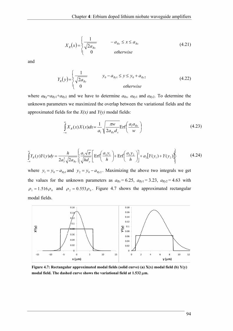
Chapter 4: Erbium doped lithium niobate waveguide amplifiers
94
otherwise
axaaxX RxRx
RxR
02
1 (4.21)
and
otherwise
ayyayayY RyRy
RyR
02
12010
(4.22)
where aRy=aRy1+aRy2 and we have to determine aRx, aRy1 and aRy2. To determine the
unknown parameters we maximized the overlap between the variational fields and the
approximated fields for the X(x) and Y(y) modal fields:
w
aa
da
w
adxxXxX Rx
xRxR
1
1
Erf2
1)()(
(4.23)
)()(ErfErf22
)()( 21223133
23
yYyYah
ya
h
ya
hd
a
aa
hdyyYyY
yRy
R
(4.24)
where 101 Ryayy and 202 Ryayy . Maximizing the above two integrals we get
the values for the unknown parameters as aRx = 6.25, aRy1 = 3.23, aRy2 = 4.63 with
01 516.1 and 02 553.0 . Figure 4.7 shows the approximated rectangular
modal fields.
Figure 4.7: Rectangular approximated modal fields (solid curve) (a) X(x) modal field (b) Y(y)
modal field. The dashed curve shows the variational field at 1.532 m.
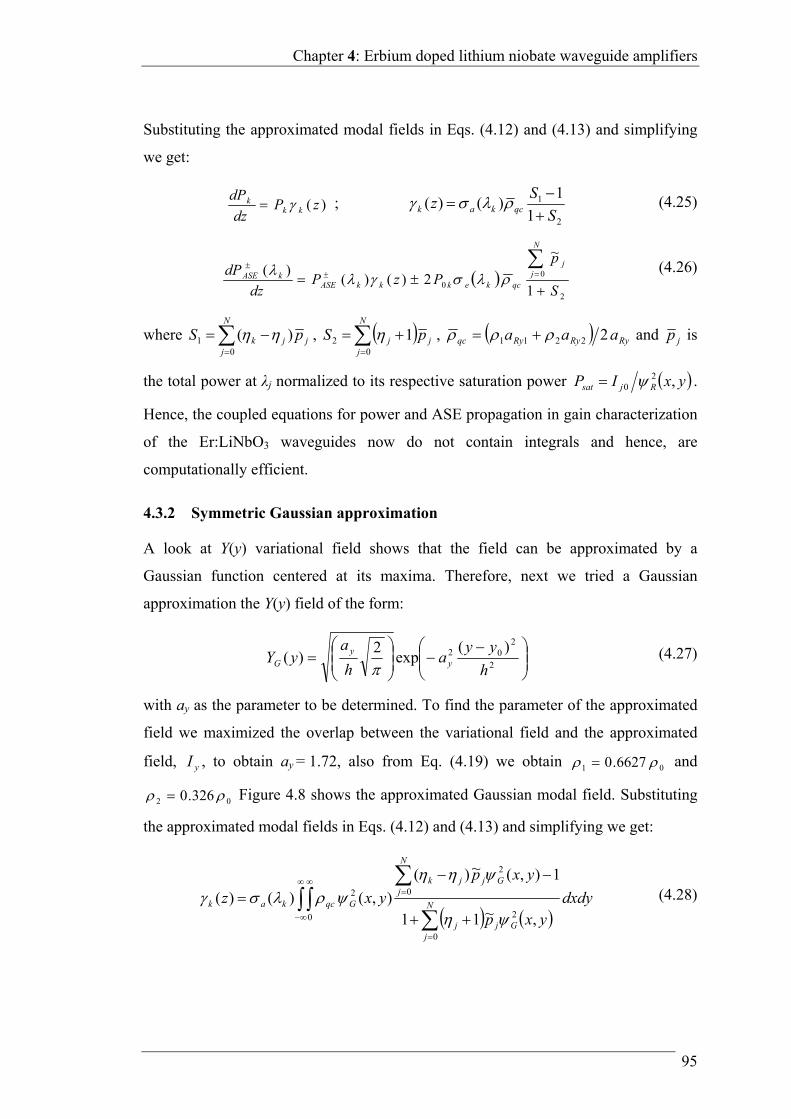
Chapter 4: Erbium doped lithium niobate waveguide amplifiers
95
Substituting the approximated modal fields in Eqs. (4.12) and (4.13) and simplifying
we get:
)( zPdz
dPkk
k ; 2
1
1
1)()(
S
Sz qckak
(4.25)
2
00 1
~
2)()()(
S
p
PzPdz
dP
N
jj
qckekkkASEkASE
(4.26)
where
N
jjjk pS
01 )( ,
N
jjj pS
02 1 , RyRyRyqc aaa 22211 and jp is
the total power at λj normalized to its respective saturation power yxIP Rjsat ,20 .
Hence, the coupled equations for power and ASE propagation in gain characterization
of the Er:LiNbO3 waveguides now do not contain integrals and hence, are
computationally efficient.
4.3.2 Symmetric Gaussian approximation
A look at Y(y) variational field shows that the field can be approximated by a
Gaussian function centered at its maxima. Therefore, next we tried a Gaussian
approximation the Y(y) field of the form:
2
202 )(
exp2
)(h
yya
h
ayY y
yG
(4.27)
with ay as the parameter to be determined. To find the parameter of the approximated
field we maximized the overlap between the variational field and the approximated
field, yI , to obtain ay = 1.72, also from Eq. (4.19) we obtain 01 6627.0 and
02 326.0 Figure 4.8 shows the approximated Gaussian modal field. Substituting
the approximated modal fields in Eqs. (4.12) and (4.13) and simplifying we get:
dxdy
yxp
yxp
yxzN
jGjj
N
jGjjk
Gqckak
0
2
0
2
0
2
,~11
1),(~)(
),()()(
(4.28)
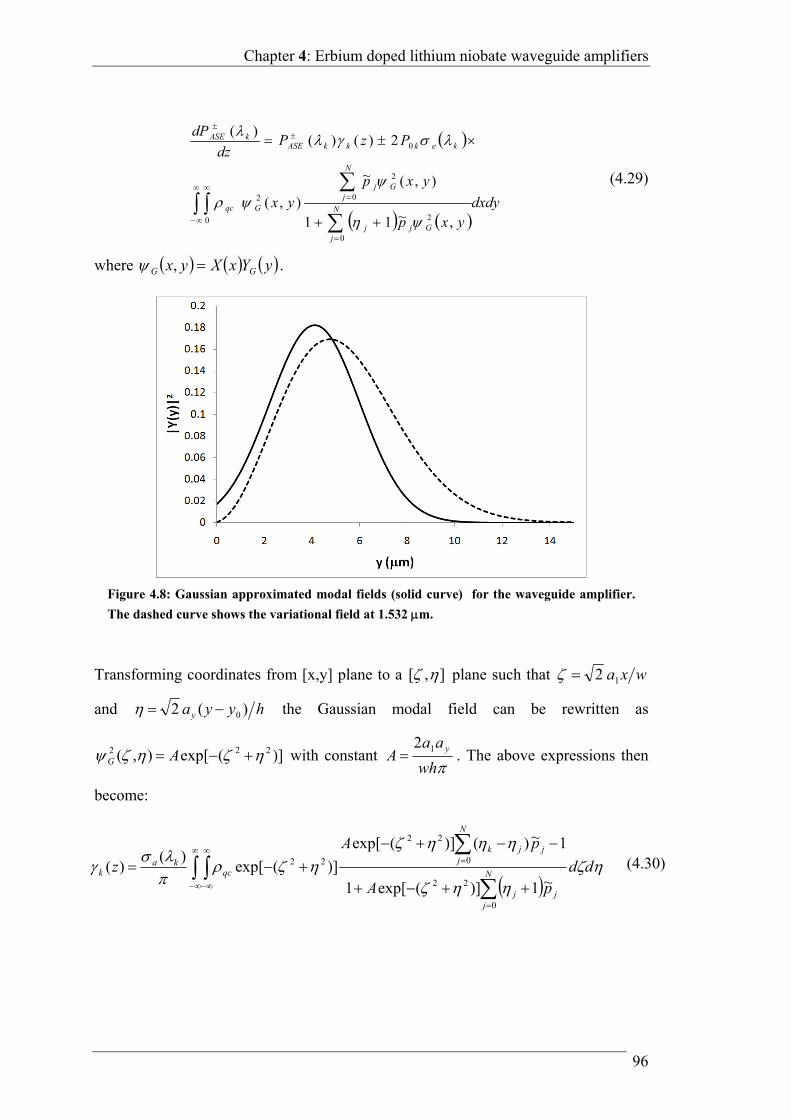
Chapter 4: Erbium doped lithium niobate waveguide amplifiers
96
dxdy
yxp
yxp
yx
PzPdz
dP
N
jGjj
N
jGj
Gqc
kekkkASEkASE
0
0
2
0
2
2
0
,~11
),(~
),(
2)()()(
(4.29)
where yYxXyx GG , .
Transforming coordinates from [x,y] plane to a ],[ plane such that wxa12
and hyyay )(2 0 the Gaussian modal field can be rewritten as
)](exp[),( 222 AG with constant wh
aaA y12 . The above expressions then
become:
dd
pA
pA
zN
jjj
N
jjjk
qcka
k
0
22
0
22
22
~1)](exp[1
1~)()](exp[
)](exp[)(
)( (4.30)
Figure 4.8: Gaussian approximated modal fields (solid curve) for the waveguide amplifier.
The dashed curve shows the variational field at 1.532 m.
Chapter 4: Erbium doped lithium niobate waveguide amplifiers
97
ddpA
pA
PzP
dz
dP
N
jjj
N
jj
qc
kekkkASE
kASE
0
22
0
22
22
0
~1)](exp[1
~)](exp[
)](exp[
2)()(
)(
(4.31)
The limits of η field have been taken as [-∞,∞] since the modal fields are negligible
after y < 0. Now we transform into polar coordinates [r,θ], resulting in
rdrdprA
prA
rzN
jjj
N
jjjk
qcka
k
0
2
0
22
0 0
2
~1]exp[1
1~)(]exp[
]exp[)(
)( (4.32)
rdrdprA
prA
r
PzP
dz
dP
j
N
jjj
N
jj
qc
kekkkASE
kASE
2
0 0
0
2
0
2
2
0
~1]exp[1
~]exp[
]exp[
2)()(
)(
(4.33)
The above two equations now contain integrals which can be solved analytically,
using 1 qc in the upper half plane ( 0 ) and 2 qc in the lower half plane
( 2 ) as shown in Figure 4.9.
Figure 4.9: Contour plot of the approximated Gaussian field for = 1.532 m.

Chapter 4: Erbium doped lithium niobate waveguide amplifiers
98
The equations thus reduce to:
21
12121 1ln)()(
S
SSSSSz qckak (4.34)
1
130
1ln2)()(
)(
S
SSPzP
dz
dPqckekkkASE
kASE
(4.35)
where
N
jjj pAS
01
~)1( ,
N
jjjk pAS
02
~)( ,
N
jjpAS
03
~ and
221 qc . Once again, the coupled equations for power and ASE propagation
now do not contain integrals and hence, are computationally efficient.
4.3.3 Asymmetric Gaussian approximation
The Y(y) variational field is asymmetric around y0, so to accommodate for the
asymmetry of Y(y) field next we choose different Gaussian about the maxima. Hence,
we approximate the variational field by an appropriately chosen Gaussian
approximation given by:
2
202
1
)(exp),(
h
yyaAyxY yyAG 0yy
2
202
2
)(exp
h
yyaA yy 0yy
(4.36)
where 2
1
21
21
2)(2
haa
aaA
yy
yyy is the normalization constant of the
approximated YAG(y) field, obtained using
1)(2 dyyYAG . Now we have to determine
ay1 and ay2. Maximizing the overlap of between the approximated Y(y) field and
variational field (Eq.4.16) gives us ay1 = 2.099 and ay2 = 1.3921. Using Eq. (4.19) we
obtain 01 798.0 and 02 27.0

Chapter 4: Erbium doped lithium niobate waveguide amplifiers
99
Figure 4.10 shows the corresponding approximated asymmetric Gaussian modal field.
Substituting the approximated modal fields in Eqs. (4.12) and (4.13) we get:
dxdy
yxp
yxp
yxzN
jAGjj
N
jAGjjk
AGqckak
0
2
0
2
0
2
,~11
1),(~)(
),()()(
(4.37)
dxdy
yxp
yxp
yx
PzPdz
dP
N
jAGjj
N
jAGj
AGqc
kekkkASEkASE
0
0
2
0
2
2
0
,~11
),(~
),(
2)()()(
(4.38)
Following an analysis similar to the one presented in Section 4.3.2, we transform
coordinates from [x,y] plane to a ],[ plane such that wxa12 and
hyyay )(2 01 for 0yy and hyyay )(2 02 for 0yy . And then
transforming to polar co-ordinates using 1 qc in the upper half plane ( 0 )
and 2 qc in the lower half plane ( 2 ) as shown in Figure 4.11 we get:
Figure 4.10: Asymmetric Gaussian approximated modal fields (solid curve) for the typical
waveguide amplifier. The dashed curve shows the variational field at 1.532 m.
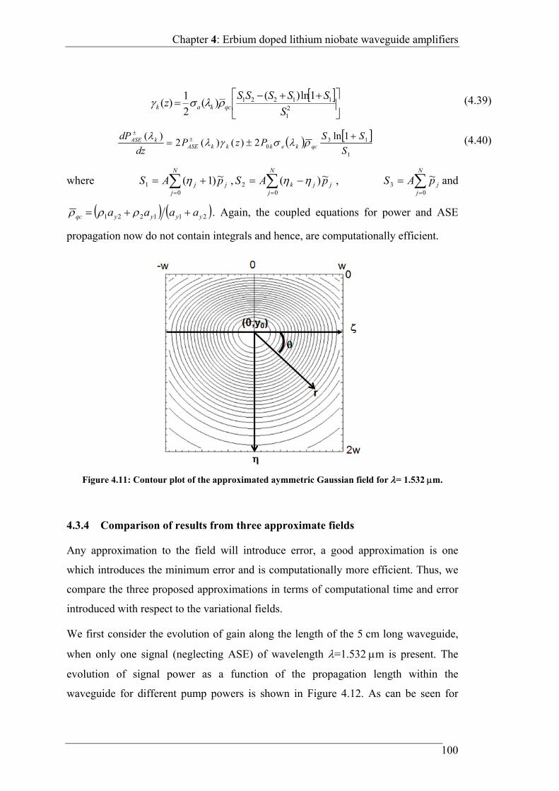
Chapter 4: Erbium doped lithium niobate waveguide amplifiers
100
21
11221 1ln)()(
2
1)(
S
SSSSSz qckak (4.39)
1
130
1ln2)()(2
)(
S
SSPzP
dz
dPqckekkkASE
kASE
(4.40)
where
N
jjj pAS
01
~)1( ,
N
jjjk pAS
02
~)( ,
N
jjpAS
03
~ and
211221 yyyyqc aaaa . Again, the coupled equations for power and ASE
propagation now do not contain integrals and hence, are computationally efficient.
4.3.4 Comparison of results from three approximate fields
Any approximation to the field will introduce error, a good approximation is one
which introduces the minimum error and is computationally more efficient. Thus, we
compare the three proposed approximations in terms of computational time and error
introduced with respect to the variational fields.
We first consider the evolution of gain along the length of the 5 cm long waveguide,
when only one signal (neglecting ASE) of wavelength =1.532 m is present. The
evolution of signal power as a function of the propagation length within the
waveguide for different pump powers is shown in Figure 4.12. As can be seen for
Figure 4.11: Contour plot of the approximated aymmetric Gaussian field for = 1.532 m.
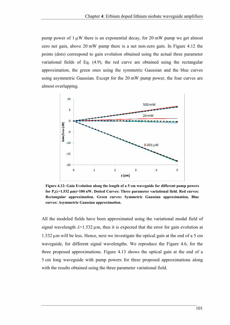
Chapter 4: Erbium doped lithium niobate waveguide amplifiers
101
pump power of 1 W there is an exponential decay, for 20 mW pump we get almost
zero net gain, above 20 mW pump there is a net non-zero gain. In Figure 4.12 the
points (dots) correspond to gain evolution obtained using the actual three parameter
variational fields of Eq. (4.9), the red curve are obtained using the rectangular
approximation, the green ones using the symmetric Gaussian and the blue curves
using asymmetric Gaussian. Except for the 20 mW pump power, the four curves are
almost overlapping.
All the modeled fields have been approximated using the variational modal field of
signal wavelength =1.532 m, thus it is expected that the error for gain evolution at
1.532 m will be less. Hence, next we investigate the optical gain at the end of a 5 cm
waveguide, for different signal wavelengths. We reproduce the Figure 4.6, for the
three proposed approximations. Figure 4.13 shows the optical gain at the end of a
5 cm long waveguide with pump powers for three proposed approximations along
with the results obtained using the three parameter variational field.
Figure 4.12: Gain Evolution along the length of a 5 cm waveguide for different pump powers
for Ps(λ=1.532 μm)=100 nW. Dotted Curves: Three parameter variational field. Red curves:
Rectangular approximation. Green curves: Symmetric Gaussian approximation, Blue
curves: Asymmetric Gaussian approximation.
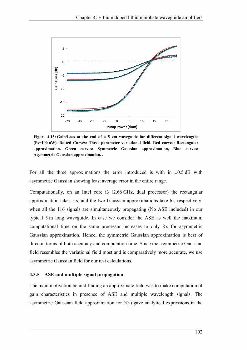
Chapter 4: Erbium doped lithium niobate waveguide amplifiers
102
For all the three approximations the error introduced is with in ±0.5 dB with
asymmetric Gaussian showing least average error in the entire range.
Computationally, on an Intel core i3 (2.66 GHz, dual processor) the rectangular
approximation takes 5 s, and the two Gaussian approximations take 6 s respectively,
when all the 116 signals are simultaneously propagating (No ASE included) in our
typical 5 m long waveguide. In case we consider the ASE as well the maximum
computational time on the same processor increases to only 8 s for asymmetric
Gaussian approximation. Hence, the symmetric Gaussian approximation is best of
three in terms of both accuracy and computation time. Since the asymmetric Gaussian
field resembles the variational field most and is comparatively more accurate, we use
asymmetric Gaussian field for our rest calculations.
4.3.5 ASE and multiple signal propagation
The main motivation behind finding an approximate field was to make computation of
gain characteristics in presence of ASE and multiple wavelength signals. The
asymmetric Gaussian field approximation for Y(y) gave analytical expressions in the
Figure 4.13: Gain/Loss at the end of a 5 cm waveguide for different signal wavelengths
(Ps=100 nW). Dotted Curves: Three parameter variational field. Red curves: Rectangular
approximation. Green curves: Symmetric Gaussian approximation, Blue curves:
Asymmetric Gaussian approximation. .
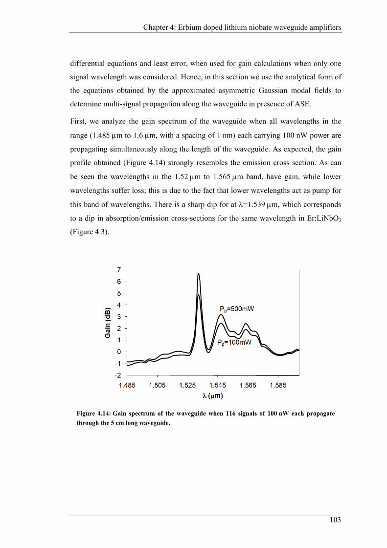
Chapter 4: Erbium doped lithium niobate waveguide amplifiers
103
differential equations and least error, when used for gain calculations when only one
signal wavelength was considered. Hence, in this section we use the analytical form of
the equations obtained by the approximated asymmetric Gaussian modal fields to
determine multi-signal propagation along the waveguide in presence of ASE.
First, we analyze the gain spectrum of the waveguide when all wavelengths in the
range (1.485 m to 1.6 m, with a spacing of 1 nm) each carrying 100 nW power are
propagating simultaneously along the length of the waveguide. As expected, the gain
profile obtained (Figure 4.14) strongly resembles the emission cross section. As can
be seen the wavelengths in the 1.52 m to 1.565 m band, have gain, while lower
wavelengths suffer loss; this is due to the fact that lower wavelengths act as pump for
this band of wavelengths. There is a sharp dip for at =1.539 m, which corresponds
to a dip in absorption/emission cross-sections for the same wavelength in Er:LiNbO3
(Figure 4.3).
Figure 4.14: Gain spectrum of the waveguide when 116 signals of 100 nW each propagate
through the 5 cm long waveguide.
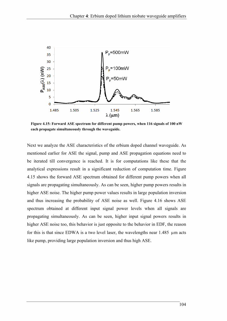
Chapter 4: Erbium doped lithium niobate waveguide amplifiers
104
Next we analyze the ASE characteristics of the erbium doped channel waveguide. As
mentioned earlier for ASE the signal, pump and ASE propagation equations need to
be iterated till convergence is reached. It is for computations like these that the
analytical expressions result in a significant reduction of computation time. Figure
4.15 shows the forward ASE spectrum obtained for different pump powers when all
signals are propagating simultaneously. As can be seen, higher pump powers results in
higher ASE noise. The higher pump power values results in large population inversion
and thus increasing the probability of ASE noise as well. Figure 4.16 shows ASE
spectrum obtained at different input signal power levels when all signals are
propagating simultaneously. As can be seen, higher input signal powers results in
higher ASE noise too, this behavior is just opposite to the behavior in EDF, the reason
for this is that since EDWA is a two level laser, the wavelengths near 1.485 m acts
like pump, providing large population inversion and thus high ASE.
Figure 4.15: Forward ASE spectrum for different pump powers, when 116 signals of 100 nW
each propagate simultaneously through the waveguide.
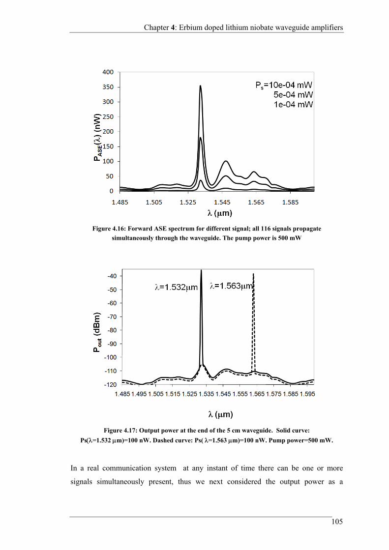
Chapter 4: Erbium doped lithium niobate waveguide amplifiers
105
In a real communication system at any instant of time there can be one or more
signals simultaneously present, thus we next considered the output power as a
Figure 4.16: Forward ASE spectrum for different signal; all 116 signals propagate
simultaneously through the waveguide. The pump power is 500 mW
Figure 4.17: Output power at the end of the 5 cm waveguide. Solid curve:
Ps=1.532 m)=100 nW. Dashed curve: Ps(=1.563 m)=100 nW. Pump power=500 mW.
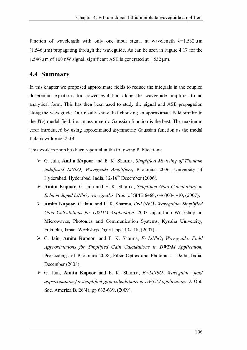
Chapter 4: Erbium doped lithium niobate waveguide amplifiers
106
function of wavelength with only one input signal at wavelength =1.532 m
(1.546 m) propagating through the waveguide. As can be seen in Figure 4.17 for the
1.546 m of 100 nW signal, significant ASE is generated at 1.532 m.
4.4 Summary
In this chapter we proposed approximate fields to reduce the integrals in the coupled
differential equations for power evolution along the waveguide amplifier to an
analytical form. This has then been used to study the signal and ASE propagation
along the waveguide. Our results show that choosing an approximate field similar to
the Y(y) modal field, i.e. an asymmetric Gaussian function is the best. The maximum
error introduced by using approximated asymmetric Gaussian function as the modal
field is within ±0.2 dB.
This work in parts has been reported in the following Publications:
G. Jain, Amita Kapoor and E. K. Sharma, Simplified Modeling of Titanium
indiffused LiNbO3 Waveguide Amplifiers, Photonics 2006, University of
Hyderabad, Hyderabad, India, 12-16th December (2006).
Amita Kapoor, G. Jain and E. K. Sharma, Simplified Gain Calculations in
Erbium doped LiNbO3 waveguides. Proc. of SPIE 6468, 646808-1-10, (2007).
Amita Kapoor, G. Jain, and E. K. Sharma, Er-LiNbO3 Waveguide: Simplified
Gain Calculations for DWDM Application, 2007 Japan-Indo Workshop on
Microwaves, Photonics and Communication Systems, Kyushu University,
Fukuoka, Japan. Workshop Digest, pp 113-118, (2007).
G. Jain, Amita Kapoor, and E. K. Sharma, Er-LiNbO3 Waveguide: Field
Approximations for Simplified Gain Calculations in DWDM Application,
Proceedings of Photonics 2008, Fiber Optics and Photonics, Delhi, India,
December (2008).
G. Jain, Amita Kapoor and E. K. Sharma, Er-LiNbO3 Waveguide: field
approximation for simplified gain calculations in DWDM applications, J. Opt.
Soc. America B, 26(4), pp 633-639, (2009).
Chapter 5: Semiconductor optical amplifiers
107
5 Semiconductor optical amplifiers
5.1 Introduction
For the last few years, telecommunication institutes around the world have shown lot
of interest in semiconductor optical amplifiers (SOA). There is a valid reason for this
interest, while on one hand, with photonics moving near to end user, SOAs are being
explored as inline amplifiers or power boosters in metropolitan computer networks,
with a tough competition between bulk-SOAs, quantum well (QW) SOAs and
quantum dot (QD) SOAs [30,31,91]. On the other hand, due to strong nonlinear
behavior SOAs appear to be a convenient tool for optical data processing [30,31,91].
For a good inline amplifier, the desired properties are high gain, high bandwidth, low
polarization sensitivity, and high saturation power, while, for optical signal processing
applications quick gain saturation and fast response times are desired.
An SOA is essentially a semiconductor laser with no reflecting facets [147]. It has a
p cladding layer, an n cladding layer and a gain region (also called active layer)
between the two (Figure 5.1). The p and n cladding regions are of high band gap as
compared to the gain region. The p-n junction is forward biased, resulting in injection
of holes from p cladding and electrons from n cladding into the gain region. Under
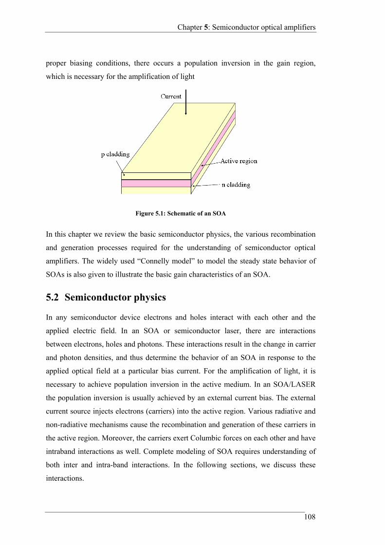
Chapter 5: Semiconductor optical amplifiers
108
proper biasing conditions, there occurs a population inversion in the gain region,
which is necessary for the amplification of light
In this chapter we review the basic semiconductor physics, the various recombination
and generation processes required for the understanding of semiconductor optical
amplifiers. The widely used “Connelly model” to model the steady state behavior of
SOAs is also given to illustrate the basic gain characteristics of an SOA.
5.2 Semiconductor physics
In any semiconductor device electrons and holes interact with each other and the
applied electric field. In an SOA or semiconductor laser, there are interactions
between electrons, holes and photons. These interactions result in the change in carrier
and photon densities, and thus determine the behavior of an SOA in response to the
applied optical field at a particular bias current. For the amplification of light, it is
necessary to achieve population inversion in the active medium. In an SOA/LASER
the population inversion is usually achieved by an external current bias. The external
current source injects electrons (carriers) into the active region. Various radiative and
non-radiative mechanisms cause the recombination and generation of these carriers in
the active region. Moreover, the carriers exert Columbic forces on each other and have
intraband interactions as well. Complete modeling of SOA requires understanding of
both inter and intra-band interactions. In the following sections, we discuss these
interactions.
Figure 5.1: Schematic of an SOA
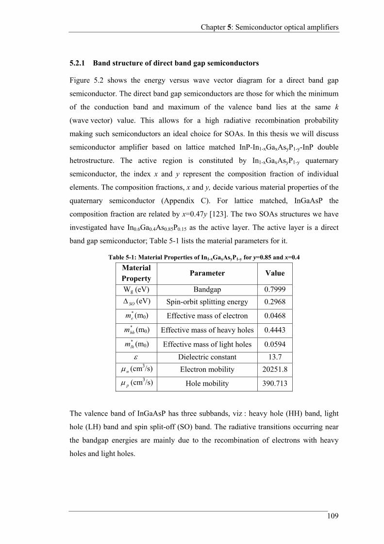
Chapter 5: Semiconductor optical amplifiers
109
5.2.1 Band structure of direct band gap semiconductors
Figure 5.2 shows the energy versus wave vector diagram for a direct band gap
semiconductor. The direct band gap semiconductors are those for which the minimum
of the conduction band and maximum of the valence band lies at the same k
(wave vector) value. This allows for a high radiative recombination probability
making such semiconductors an ideal choice for SOAs. In this thesis we will discuss
semiconductor amplifier based on lattice matched InP-In1-xGaxAsyP1-y-InP double
hetrostructure. The active region is constituted by In1-xGaxAsyP1-y quaternary
semiconductor, the index x and y represent the composition fraction of individual
elements. The composition fractions, x and y, decide various material properties of the
quaternary semiconductor (Appendix C). For lattice matched, InGaAsP the
composition fraction are related by x=0.47y [123]. The two SOAs structures we have
investigated have In0.6Ga0.4As0.85P0.15 as the active layer. The active layer is a direct
band gap semiconductor; Table 5-1 lists the material parameters for it.
Table 5-1: Material Properties of In1-xGaxAsyP1-y for y=0.85 and x=0.4
Material Property
Parameter
Value
Wg (eV) Bandgap 0.7999
SO (eV) Spin-orbit splitting energy 0.2968 *em (m0) Effective mass of electron 0.0468 *hhm (m0) Effective mass of heavy holes 0.4443 *lhm (m0) Effective mass of light holes 0.0594
Dielectric constant 13.7
n (cm3/s) Electron mobility 20251.8
p (cm3/s) Hole mobility 390.713
The valence band of InGaAsP has three subbands, viz : heavy hole (HH) band, light
hole (LH) band and spin split-off (SO) band. The radiative transitions occurring near
the bandgap energies are mainly due to the recombination of electrons with heavy
holes and light holes.
Chapter 5: Semiconductor optical amplifiers
110
In the vicinity of 0k , the energy bands (both conduction band and valence band)
can be approximated by parabola [126,147], thus we can write the energy of electron
in conduction band eW and energy of hole4 in valence band hW as:
*
22
2 e
eCe
m
kWW
(5.1)
*
22
2 h
hVh
m
kWW
(5.2)
where hek , are the magnitudes of the wavevectors of a given electron or hole, *,hem is
the effective mass, CW is the conduction band edge energy and VW the valence band
edge energy, ( VCg WWW is the bandgap energy). When an electron at energy eW
makes a downward transition from the conduction band to the valence band
energy hW , a photon of frequency f is emitted. Considering that momentum is
4 Electrons in the upper valence band edge have a negative effective mass. An electron with negative charge and negative effective mass can be equivalently substituted by a particle of positive charge and positive effective mass, the so called hole.
Figure 5.2: Energy vs. wave vector diagram for a direct bandgap semiconductor

Chapter 5: Semiconductor optical amplifiers
111
conserved in the transition, i.e., kkk he
the energy of the emitted photon is given
by:
rghe m
kWWWhf
2
22 (5.3)
where
1
**
11
her mm
m is the reduced mass. From Eq. (5.3) we can determine the
momentum term k , substituting in Eqs. (5.1) and (5.2), the conduction and valence
band energies can be rewritten as:
gCe WhfrWW (5.4)
gVh WhfrWW 1 (5.5)
with *** 1
1
hee
r
mmm
mr
. In the above expressions, h is the Planck’s constant, and
2h is the reduced Planck’s constant. It should be remembered that the above
expressions are valid under the parabolic band approximation, and when the
momentum in the transition is conserved.
5.2.2 Electron and hole concentration
To determine the electro-optic behavior of the semiconductor materials it is important
to determine the electron and hole concentrations available for conduction. The
electrons and hole occupying the conduction band and valence band can be
determined by the knowledge of two parameters: density of states )(W and the
occupancy probability )(Wf . Electrons and holes obey Pauli’s exclusion principle;
therefore the occupation probability of electrons and holes is given by the Fermi-Dirac
function. The probability that energy state W is occupied by an electron is given by the
Fermi function:
1
exp1)(
Tk
WWWf
B
F (5.6)
where WF is called the Fermi level. It represents the energy where the occupation
probability f(W) becomes half at all temperatures. In a p-n junction under thermal

Chapter 5: Semiconductor optical amplifiers
112
equilibrium, the same Fermi level characterizes the majority and minority carrier
concentrations, i.e., it is same throughout the semiconductor. However, when the
carriers are injected into the semiconductor, the equilibrium is disturbed, and the
Fermi levels split. The carrier density can no longer be described by a constant Fermi
level, instead we define non-equilibrium quasi Fermi levels FnW and FpW for
electrons and holes respectively. Thus, the probability that electron states of energy of
eW and hW are occupied is determined by:
1
exp1)(
Tk
WWWf
B
Fneec and
1
exp1)(
Tk
WWWf
B
Fphhv (5.7)
Let )( eC W be the density of states (DOS) of conduction band, and )( hV W DOS of
valence band. DOS, dWW determines the number of possible energy states within
eW and ee dWW , per unit volume, and Fermi function determines the occupancy
probability. Therefore, the number of electrons occupying the conduction band Tn and
number of holes p occupying the valence band can be determined by:
eW
eeceCT dWWfWn )()( (5.8)
hW
hhvhV dWWfWp ))(1)(( (5.9)
The density of states )( eC W and )( hV W for electrons in the conduction band and
holes in valence band respectively has the form [126]:
21
23
2
*24)( Ce
eeC WW
h
mW
Ce WW (5.10)
21
23
2
*24)( hV
hhV WW
h
mW
Vh WW (5.11)
Substituting Eqs. (5.10) and (5.11) and Fermi functions in the carrier concentration
equation we get:
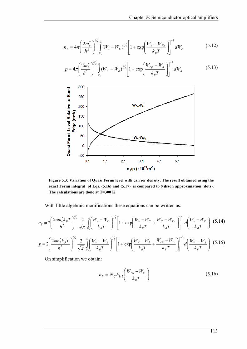
Chapter 5: Semiconductor optical amplifiers
113
eW
eB
FneCe
eT dW
Tk
WWWW
h
mn
1
21
23
2
*
exp1)(2
4 (5.12)
eW
hB
hFphV
h dWTk
WWWW
h
mp
1
21
23
2
*
exp1)(2
4 (5.13)
With little algebraic modifications these equations can be written as:
eW B
Ce
B
FnC
B
Ce
B
CeBeT Tk
WWd
Tk
WW
Tk
WW
Tk
WW
h
Tkmn
12
12
3
2
*
exp122
2
(5.14)
eW B
hV
B
VFp
B
hV
B
hVBh
Tk
WWd
Tk
WW
Tk
WW
Tk
WW
h
Tkmp
12
12
3
2
*
exp122
2
(5.15)
On simplification we obtain:
Tk
WWFNn
B
CFnCT 2/1 (5.16)
Figure 5.3: Variation of Quasi Fermi level with carrier density. The result obtained using the
exact Fermi integral of Eqs. (5.16) and (5.17) is compared to Nilsson approximation (dots).
The calculations are done at T=300 K
Chapter 5: Semiconductor optical amplifiers
114
Tk
WWFNp
B
FpVV 2/1 (5.17)
Here, 2/32*22 hkTmN eC , 2/32*22 hkTmN hV are the effective densities of
conduction band and valence band respectively, and dxe
xF
x
0
2/1 1
2
is the
Fermi integral of order 2/1 . The expressions of Eqs. (5.16) and (5.17) are used to
determine the position of the quasi Fermi levels, once the carrier densities Tn and p
are known. Fermi integral in the expression can be either solved using numerical
integration techniques [100], or we can use one of the available approximations to
evaluate it. A widely used estimate is the empirical approximation given by
Nilsson [93].
TkWW BCCCCCFn
4/16405524.064ln
TkWW BVVVVFpV
4/16405524.064ln
(5.18)
where, CTC Nn / and VV Np / . Figure 5.3 compares the quasi Fermi levels
obtained using the exact integral with values obtained using Nilsson approximation
Eq. (5.18).
5.2.3 Generation and recombination processes
Electrons in the conduction band combine with holes in the valence band (i.e.,
deexcite to the valence band) or vice versa, resulting in emission or absorption of
photons, Figure 5.2 shows one such radiative transition (recombination). The electron
recombines with the hole, releasing the excess energy as photon. As discussed in
Section 2.6.1, there are three radiative processes important in any optoelectronic
devices: spontaneous emission, stimulated absorption and stimulated emission (Figure
5.4). Beside the three radiative transitions there are some non-radiative transitions as
well, which tend to reduce the carrier density. Auger recombination and Shockley
Read Hall recombination are two important non-radiative transitions.
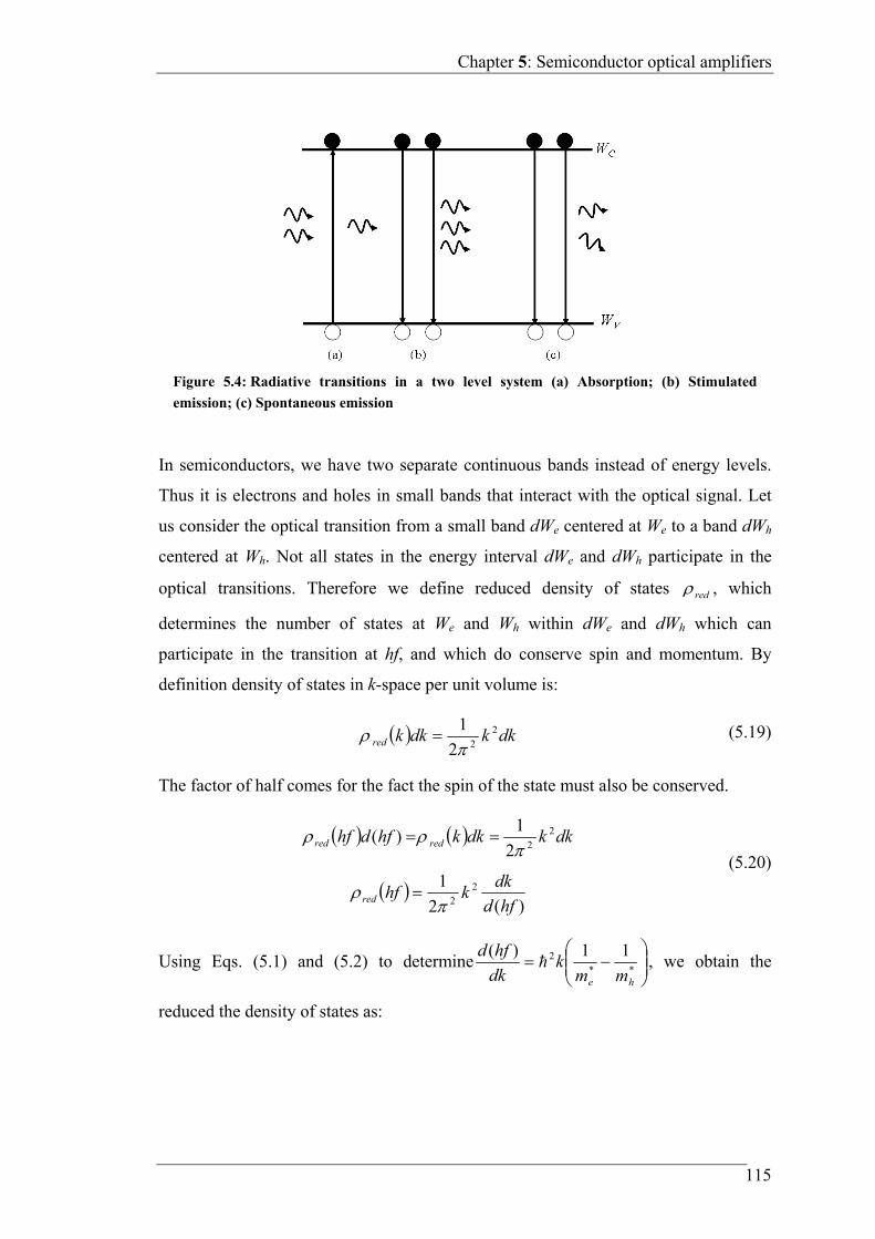
Chapter 5: Semiconductor optical amplifiers
115
In semiconductors, we have two separate continuous bands instead of energy levels.
Thus it is electrons and holes in small bands that interact with the optical signal. Let
us consider the optical transition from a small band dWe centered at We to a band dWh
centered at Wh. Not all states in the energy interval dWe and dWh participate in the
optical transitions. Therefore we define reduced density of states red , which
determines the number of states at We and Wh within dWe and dWh which can
participate in the transition at hf, and which do conserve spin and momentum. By
definition density of states in k-space per unit volume is:
dkkdkkred2
22
1
(5.19)
The factor of half comes for the fact the spin of the state must also be conserved.
dkkdkkhfdhf redred2
22
1)(
)(2
1 22 hfd
dkkhfred
(5.20)
Using Eqs. (5.1) and (5.2) to determine
**2 11)(
he mmk
dk
hfd , we obtain the
reduced the density of states as:
Figure 5.4: Radiative transitions in a two level system (a) Absorption; (b) Stimulated
emission; (c) Spontaneous emission
Chapter 5: Semiconductor optical amplifiers
116
gr
red Whfh
mhf
3
2/3
2
8 (5.21)
In this section we discuss all the five processes, involving inter-band transitions.
5.2.3.1 Absorption
An electron in the valence band can be excited by optical, electrical or thermal means
to make an upward transition to the conduction band. In SOAs, the population
inversion is achieved by electrical means, but still the presence of photons with energy
greater then bandgap can excite the electrons. When an electron absorbs a photon and
jumps to the conduction band, the process is referred as stimulated absorption (Figure
5.4 a). This process results in the generation of an electron-hole pair. If dffPh )( is
the energy density of photons between f and f + df causing the optical transitions,
hfred reduced density of states, hV Wf determines occupancy probability of
lower energy state Wh, and eC Wf1 determines that the upper energy state We is
empty, then the absorption rate ( 13sm ) , i.e., the rate at which photons are absorbed,
or electrons (holes) are generated can be given by5 [126,135,147]:
))(1)(()(12 eChVredPhastim WfWfhfdffBR (5.22)
5.2.3.2 Stimulated emission
An electron in the conduction band can be induced to undergo a downward transition
by the presence of photons by the process of stimulated emission (Figure 5.4 b). This
will result in generation of an additional photon coherent with the initial photon, and
annihilation of the electron hole pair. The process is exactly analogous to the
absorption process, but in reverse direction. Thus, stimulated emission rate ( 13sm ),
i.e., the rate at which photons are emitted, or electrons (holes) are annihilated can be
given by [126,135,147]:
5 In semiconductors we are dealing with electrons and holes, they are Fermions as oppose to atoms , which are Boson particles. Thus from Pauli’s exclusion principle, there is only one way an electron and an hole can occupy an energy state, i.e. g2=g1. Also instead of number of atoms, we consider the reduced density of states and occupancy probability.
Chapter 5: Semiconductor optical amplifiers
117
))(1)(()(21 hVeCredPhestim WfWfhfdffBR (5.23)
5.2.3.3 Spontaneous emission
An electron in the conduction band can also make a spontaneous downward transition
to the valence band; this is referred as spontaneous emission (Figure 5.4 c). The
process results in the generation of photons and annihilation of electron-hole pair. The
photon so produced has random amplitude and random phase. Mathematically, the
spontaneous recombination rate ( 13sm ) is expressed [135] as
heCredsp WfWfhfAhfWr 121 (5.24)
This expression includes all the spontaneous transitions, around the center frequency f.
Thus the total spontaneous emission will be sum over all possible frequencies. Thus
we have:
hfdhfrR spsp (5.25)
Assuming a non-degenerate semiconductor, and also assuming there is no k-selection
rule, then total spontaneous emission can be simply given by [9,76],:
pBnR Tsp (5.26)
where B is the bimolecular radiative recombination coefficient. The bimolecular
coefficient is related with the Einstein coefficient A21 by expression:
BpA 21 (5.27)
Here we should mention the fact that while total spontaneous emission reduces the
carrier density, only some fraction of the photons emitted in this transition couple to
the propagating waveguide mode. The emission factor Q (Section 5.3.3 Eq. (5.50))
determines the fraction of spontaneously emitted photons coupled to the propagating
wave guide mode.
5.2.3.4 Auger recombination
Auger recombination is the result of electron-electron interaction. Here an electron
recombines with a hole and transfers the energy thus released to another electron (or
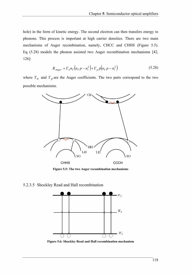
Chapter 5: Semiconductor optical amplifiers
118
hole) in the form of kinetic energy. The second electron can then transfers energy to
phonons. This process is important at high carrier densities. There are two main
mechanisms of Auger recombination, namely, CHCC and CHHS (Figure 5.5).
Eq. (5.28) models the phonon assisted two Auger recombination mechanisms [42,
126]:
22iTpiTTnAuger npnpnpnnR (5.28)
where n and p are the Auger coefficients. The two parts correspond to the two
possible mechanisms.
5.2.3.5 Shockley Read and Hall recombination
Figure 5.5: The two Auger recombination mechanisms
Figure 5.6: Shockley Read and Hall recombination mechanism
Chapter 5: Semiconductor optical amplifiers
119
This type of recombination occurs when an electron/hole falls into a trap. The crystal
impurities in the form of defect or foreign atom results in formation of trap levels
within the bandgap. The process can be envisioned as a two step transition of an
electron from the conduction band to the valence band, or as the annihilation of the
electron and hole pair which meet each other in the trap (Figure 5.6). This is a
dominant recombination process in indirect bandgap materials like silicon. If TW is
the energy of the trap state, then the Shockley Read and Hall recombination rate is
modeled using the relation [108]:
Tk
WWpp
Tk
WWnn
npnR
B
TVin
B
TCiTp
iTSRH
expexp
2
(5.29)
where n and p are the electron and hole lifetimes.
5.2.4 Intra band interactions
We have already discussed the transition of electrons between conduction and valence
band, either involving photons (radiative) or without them (non-radiative). Besides
these interband interactions, the electrons (or holes) in the same energy band can
interact with each other and modify the energy states. These interactions are referred
as intraband interactions. In general, three such interactions play a major role in
influencing the behavior of an SOA, namely: free carrier absorption, Burstein-Moss
effect, and bandgap shrinkage.
5.2.4.1 Bandgap narrowing
The many body interaction (electron-electron, electron-impurity, hole-hole, hole-
impurity) in semiconductors can also cause the change in the bandgap of the
semiconductor. This phenomenon is known as bandgap narrowing (BGN) effect.
These interactions result in wave functions to overlap and the particles tend to occupy
new energy states of lower energy. The net result is decrease in the energy of the
Chapter 5: Semiconductor optical amplifiers
120
conduction band edge, and increase in the energy of the valence band edge. For an
SOA, it is important for us to consider BGN because it affects the region of the
spectrum where absorption and gain is high. According to Wolff [142] the shift in
band gap can be expressed as:
3/13/13/13/13/12 3
2pn
dn
dWpn
eW T
gTg
(5.30)
where gW is the band gap energy. From this expression, we
get eVm1035.2/ 10dndWg for lattice matched InP-InGaAsP. However,
experiments carried out in [15] do not confirm to such a high value. According to an
estimate by Agrawal [6] eVm106.1/ 10dndWg , this value is confirmed by the
experiments in [77], so we use this value for the bandgap shrinkage.
5.2.4.2 Burstein Moss effect
The Burstein-Moss effect [135] or band filling is observed as an increase in the band
gap in the degenerate semiconductors. It arises from the fact that electrons being
fermions, obey Pauli’s exclusion principle. In degenerate semiconductors, the Fermi
energy (WF) lies in the conduction band for heavy n-type doping (or in the valence
band for p-type doping). The filled states therefore block thermal or optical excitation.
Consequently the measured band gap determined from the onset of interband
absorption moves to higher energy (i.e. suffers "a blue shift"). The shifted band gap for
n type degenerate semiconductor is given by:
*
*
*
3/23/222' 1
2
)3(
h
e
egg
m
m
m
nWW
(5.31)
Since the shift in bandgap depends on */1 m , the effect is more prominent in n-type
degenerate semiconductors as compared to p-type semiconductor.
5.2.4.3 Free carrier absorption
The electrons in the same band can absorb the photons and move up from low energy
state to high energy state in the same band. In the process, momentum is conserved by
Chapter 5: Semiconductor optical amplifiers
121
the presence of a third particle phonon (or impurities). Since the carriers in the same
energy band in semiconductors behave very similar to the free electrons in metals,
thus the Drude Model [12,144] is generally employed to determine the absorption loss
of photons due to these free carriers. The free carrier absorption coefficient is thus
given by following expression, for electrons and holes respectively.
nnTnfc
mnc
e
20
32
23
,4
pp
pfcpmc
e
20
32
23
,4
(5.32)
5.3 Semiconductor optical amplifiers
5.3.1 Condition for amplification
The semiconductor will act as an amplifier for light if there is net stimulated emission,
or in other words when: astim
estim RR , from (5.22) and (5.23) we get:
)(1)()(1)( echvhvec WfWfWfWf (5.33)
Using the definition of Fermi function (defined in Section 5.2.2), the above condition
reduces to:
FpFnhe WWWWhf (5.34)
Furthermore, we know that the photon energy has to be greater than the bandgap, for
radiative transition to take place; therefore, we get a condition for amplification in
semiconductors [31,42,126]:
FpFng WWhfW (5.35)
Thus for amplification of the photon signal of frequency f to take place, the p-n
junction should be biased such that the separation of quasi Fermi levels exceeds the
bandgap. This is possible only if either both or at least one of the quasi Fermi level
crosses the band.
Chapter 5: Semiconductor optical amplifiers
122
5.3.2 Optical gain
Eq. (5.23) represents the downward transition of electrons occurring per second per
unit volume, in response to a flux of incoming photons in a given optical mode.
Similarly, (5.22) represents the upward transition. For optical amplification to take
place, downward transitions should be greater than the upward transitions. If we
suppose, that an electromagnetic wave is propagating in z direction, then the net
increase in the photon flux hf
vdfff g
(number of photons PhN crossing per
unit area per second, 12sm ) per unit length along the z direction can be written as:
astim
estim RR
dz
fd
(5.36)
The optical gain of the material is normally defined as the fractional increase in the
photons per unit length [147], i.e.
f
RR
dz
fd
ffg
astim
estim
m
1
(5.37)
From Eqs. (5.37), (5.22) and (5.23) we can derive an expression of the gain as
[135,147]:
hvecredm WfWfhfhfBfg 21 (5.38)
Here we used the fact that 1221 BB . Using the relationship between the Einstein A
and B coefficients we can rewrite the gain as:
hvecredspg
m WfWfhfnn
cfg
2
2
8 (5.39)
where 21/1 Asp is the spontaneous carrier recombination lifetime. It depends on the
material and is also a function of carrier density
From Eq. (5.39), it is clear that the gain depends on both the signal wavelength and
carrier density. Figure 5.7 shows a plot of material gain coefficient for a lattice
matched InP-InGaAsP material. For wavelengths above the bandgap wavelength
gg Whc / there is no gain, as these wavelengths do not satisfy the condition for
amplification (Section 5.3.1). The material gain drops below zero for small

Chapter 5: Semiconductor optical amplifiers
123
wavelengths, signifying that at these wavelengths absorption exceeds the emission. As
the injection current is increased, the gain coefficient and the bandwidth increase as
well. Increase in the carrier density lowers the minimum wavelength observing non-
zero gain; this is so because the quasi-Fermi levels are pushed deep into their
respective bands. Due to the effect of bandgap shrinkage signals with wavelength
greater than the bandgap wavelength at no bias also experience a gain.
Spectral broadening: The discussion above assumes that an electron in the conduction
band will stay in conduction band forever, unless there is interaction with photons. In
reality, this is not true; electrons interact with each other and phonons resulting in
scattering. In other words, electrons do not stay in the same energy state for infinity;
rather they scatter into a new energy state every few pico-seconds. For μm55.1
InGaAsP, these relaxation times of the order of fs100 are reported [53]. Hence,
energy of each transition is no longer sharp but has energy spread over a range of
meV7fs100 W on each side. If we assume an exponential decay with time,
then the spread can be represented by Lorentzian lineshape function:
Figure 5.7: Material gain coefficient as a function of wavelength, for different carrier
densities.
Chapter 5: Semiconductor optical amplifiers
124
22
1)(
in
in
hfWW
L (5.40)
where in is the intraband relaxation time. The spectral broadening is included by
convolving the gain given by (5.39) with the Lorentzian lineshape function over all
transition energies i.e. [147]:
dWWfgf m L (5.41)
Effect of gain on signal and spontaneous emission: If sigS is the photon density
incident on the amplifier, propagating with a group velocity gv , and the active region
material exhibits an optical gain mg at the incident photon frequency f 6, then for a
small length of amplifier, the transition rate of carriers due to stimulated processes can
be written as:
sigsigmgst RSgvR (5.42)
Depending on the sign of mg , the dominating process is either stimulated emission
(positive mg ) or stimulated absorption (negative mg ). The photons generated by the
process of spontaneous emission can further induce stimulated emissions. In other
words, the photons generated by the process of spontaneous emission can also
undergo amplification, just like the optical signal. This further reduces the carrier
density, and the resultant optical signal is called amplified spontaneous emission
(ASE). These photons propagate through the waveguide in the same fashion as signal
photons. If ASES is the photon density due to amplified spontaneous emission, then
the recombination rate of carriers due to these photons will be
ASEmgASE SgvR (5.43)
Since these photons have random phase and direction, they are the inherent noise in
any optical amplifier. It is impossible to eliminate this noise.
6 We concentrate on the response of an SOA to a single frequency f, therefore, for simplicity we replace gm(f)~gm

Chapter 5: Semiconductor optical amplifiers
125
5.3.3 Rate equations
In an SOA there is an interaction between the optical signal (electromagnetic field )
and the applied electric potential V . In this section, we consider the various rate
equation governing the pulse propagation and amplification in an SOA [81,62]. The
modal field ),( yxp of the pth mode satisfies the Helmholtz equation (Section 2.3).
0),(),( 222
2
2
2
yxyxkyx pppm (5.44)
),( yxp is the normalized as 1,
dydxyxp , ck mm / is the free space
wave vector, m is the angular frequency of the longitudinal mode m, and p is the
propagation constant for the pth mode. Since we take into account only the
fundamental transverse mode, we drop the subscript p.
Next thing that follows is Poisson’s equation, if V is the applied electrostatic
potential, charge density, and the permittivity of the medium than we have
0
2
),(
yxV
r
(5.45)
If the pn JJJ
is the current density, then the rate by which the electron density
Tn , the hole density p and photon densities totS will change is given by
sigASEspAugerSRHnT RRRRRJdiv
et
n
1
(5.46)
sigASEspAugerSRHp RRRRRJdivet
p
1
(5.47)
SPph
mtotm
totmg
mtot QR
SSgv
dt
dS
(5.48)
where mirrpfcnfcagph
dydxyxpndydxyxv
2
,,
2),(),(
1, and
mASE
msig
mtot SSS is the total photon density. The superscript ‘m’ refers to the different
longitudinal modes. In (5.46) and (5.47) the first term refers to the increase in the
carrier density by the injection current. The second term in the bracket refers to the
Chapter 5: Semiconductor optical amplifiers
126
decrease in the carrier density due to the combined effect of radiative (only
spontaneous) and non-radiative recombinations. The third term corresponds to the
decrease in the carrier density due to stimulated emission of carriers induced by the
presence of photons. These three together determine the rate at which the carrier
density changes with time.
Eq. (5.48) determines the rate at which the photon density changes with time. Each
term in (5.47), causing a change in the carrier density due to interaction with photons
has a corresponding term in (5.48). The first term on the right hand side of (5.48)
accounts for the gain (loss) in the photon density due to stimulated emission
(absorption) of photons, this term corresponds to the third term in (5.47) with a
multiplicative factor . This is so, because the carriers and the photons occupy
different overlapping volumes. Only the photons overlapping with the optical electric
modal field yx, contribute to the change in photon density. The confinement
factor is defined as
dxdyyx
dxdyyxd w
2
0 0
2
),(
),(
(5.49)
where w is the width of the ridge waveguide, and d the height of the active layer. The
second term in (5.48) takes care of the different various loss mechanisms which result
in the decrease in photon density. They are altogether summed up via the photon
lifetime ph . (The different loss mechanisms are bulk absorption loss, two photon
absorption loss and the mirror loss. The mirror loss is expressed as
frmirr RRL
1ln
2
1 , where rR and fR are the rear and front mirror reflectivities
and L is the length of the amplifier.).
The last term in (5.48) corresponds to the increase in photons due to spontaneous
emission. The factor Q , also known as emission factor, is needed as only a small
fraction of the total spontaneously emitted photons contributes to the guided mode.
Taking into account the confinement factor , the ratio of spontaneous radiative
Chapter 5: Semiconductor optical amplifiers
127
recombination rate spR into one mode and the total recombination rate
SRHAugsptot RRRR , defines Q:
tot
sp
R
RQ
(5.50)
In (5.46) and (5.47) the current densities for the electron and hole nJ and pJ are given
by the drift diffusion model as
),( tzngradTkVVgradenJ TnBnnTn
(5.51)
),( tzpgradTkVVgradepJ pBppp
(5.52)
where the currents are composed of drift and diffusion terms respectively, n and
p are position dependent electron and hole mobility, nV and pV are the electron and
hole band parameters defined as ieB
pn ne
TkVV ln , Bk is the Boltzmann constant, T
is the temperature, e is the elementary charge, and ien is effective intrinsic carrier
concentration. nV and pV accounts for the gradient in the effective intrinsic carrier
concentration, which can take care of the bandgap narrowing effect.
In order to reach a solution it is necessary to solve the differential equations (5.45-
5.48) self consistently. Finally, power variation along length is determined using the
amplifier equation [42]:
Pgdz
dPm (5.53)
where constitutes the losses to the optical signal.
5.3.4 SOA modeling: Connelly model
Several models have been developed in the past to simulate SOAs [81,62,30,31,23],
depending on the behavior we want to simulate, one model can be better than others.
In general, they all solve rate equations, i.e., time dependent differential equations for
the carrier and photons, and either, average the carrier density over the entire length of
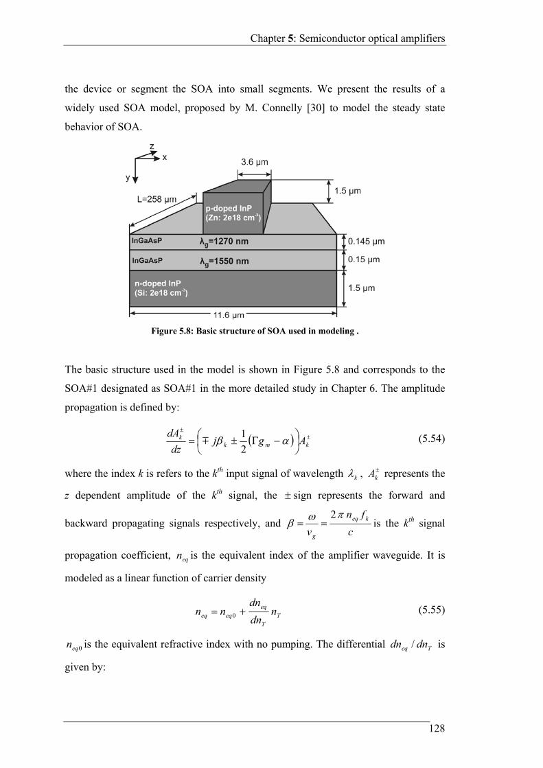
Chapter 5: Semiconductor optical amplifiers
128
the device or segment the SOA into small segments. We present the results of a
widely used SOA model, proposed by M. Connelly [30] to model the steady state
behavior of SOA.
The basic structure used in the model is shown in Figure 5.8 and corresponds to the
SOA#1 designated as SOA#1 in the more detailed study in Chapter 6. The amplitude
propagation is defined by:
kmk
k Agjdz
dA
2
1 (5.54)
where the index k is refers to the kth input signal of wavelength k , kA represents the
z dependent amplitude of the kth signal, the sign represents the forward and
backward propagating signals respectively, and c
fn
vkeq
g
2
is the kth signal
propagation coefficient, eqn is the equivalent index of the amplifier waveguide. It is
modeled as a linear function of carrier density
TT
eqeqeq n
dn
dnnn 0 (5.55)
0eqn is the equivalent refractive index with no pumping. The differential Teq dndn / is
given by:
Figure 5.8: Basic structure of SOA used in modeling .
Chapter 5: Semiconductor optical amplifiers
129
TeqT
eq
dn
dn
n
n
dn
dn
20
(5.56)
Here, n is refractive index of the active region. The z-dependent amplitude kA are
subject to boundary conditions:
)0()1()0( 11 zArArzA kink k
)()( 21 LzArLzA kk (5.57)
If inkP is the input signal power for the kth signal, and out
kP is the corresponding output
power, in and out are the input and output coupling efficiencies, then we have
relations:
k
inkin
k hf
PzA
)0(
)()1( 2 LzArLzA kk
(5.58)
The kth output signal power after considering the coupling loss is thus:
2LzAhfP koutk
outk (5.59)
In the Connelly Model, the ASE is accounted by defining photon rate equations, as
opposed to amplitude rate equations for signals. Thus, ASES will obey the travelling
wave equation:
spASEmASE QRSg
dz
dS
spASEmASE QRSg
dz
dS
(5.60)
The sign represents the forward and backward propagating ASE respectively.
Further, the carrier density at each z obeys the rate equation
ASEsigTT RRznR
ed
J
dt
zdn )(
)( (5.61)
where R(nT(z)) includes both radiative and non-radiative (Auger and SRH)
recombinations.
Chapter 5: Semiconductor optical amplifiers
130
32 1))(( TnT
nTT nnBnznR
(5.62)
The explanation for the three terms in RHS is as follows: the first term corresponds to
rate of radiative recombinations, the second term corresponds to SRH recombination
rate, and the third term is Auger recombination rate.
The SOA of length L is segmented into small sections of length dz (Figure 5.9), in
each of these sections under steady state conditions the RHS of above equation will be
zero. As the first step, the signal fields and spontaneous emission photon rates are
initialized to zero. The initial carrier density is obtained from above equation with no
optical signal. Next we compute the coefficients for the Eqs. (5.54). The signal fields
and noise photon densities are then estimated. Then we iterate for the carrier density
such that RHS of Eq. (5.61) is zero throughout the SOA. The iteration continues until
the percentage change in signal fields, noise photon rates, and carrier density
throughout the SOA between successive iterations is less than the desired tolerance.
Table 5-2 lists the parameters used for modeling7.
7 We model two SOAs, SOA#1 and SOA#2 respectively; the detailed structure of the two SOAs is described in next chapter.
Figure 5.9: The ith section of the SOA model.
Chapter 5: Semiconductor optical amplifiers
131
Table 5-2: Parameters used for modeling the SOA
Symbol Parameter Value SOA#1
y Mole fraction of Arsenide in the active region 0.85
L Active region length 258 m
d Active region thickness 0.145 m
w Active region width 3.6 m
Optical confinement factor 0.2
Kg Bandgap shrinkage coefficient 1.6x10⁻¹⁰ eVm
n1 InGaAsP refractive index 3.47
n2 InP refractive index 3.1
neq0 Equivalent refractive index at zero carrier
density 3.22
dn/dnT Differential of active region refractive index
with respect to carrier density -1.8x10⁻²⁶ m-3
in Input coupling loss 5 dB
out Output coupling loss 5 dB
Losses 6000 m-1
R1 Input facet reflectivity 10-4
R2 Output facet reflectivity 10-4
n Carrier lifetime 10-9 s
B Bimolecular radiative recombination coefficient 8.5x10⁻¹⁶ m3/s
n Auger recombination coefficient 3.535x10-41 m6/s
The material parameters specific for InxGa1-xAsyP1-y are given in Appendix C.
Figure 5.10: Output power vs input power for SOA#1 at different injection currents.
Chapter 5: Semiconductor optical amplifiers
132
Figure 5.10 shows the variation of output power as the input power to the SOA is
varied for SOA#1 at different injection currents. The curve shows that initially output
power increases linearly with the input power, but at high input powers the output
power starts saturating. Thus optical gain of an SOA is not constant but decreases as
the input optical power increases. This is referred as gain saturation. The input
(output) optical power at which the gain of the amplifier reduces to half of the small
signal gain is called as the input (output) saturation power satinP ( sat
outP ). Figure 5.11 and
Figure 5.12 show the input and output saturation power for the SOA at an injection
current of 100 mA.
While the Connelly Model can give a good approximation of the behavior of an SOA,
one has to assume values of some important SOA parameters like , Tdndn / , loss
coefficient etc. Any modification in the design or operating point requires refitting
of theses parameters. Moreover, the model is valid for an intrinsic active layer. Lastly,
though it accounts for bandgap narrowing effect, it fails as the carrier density
increases, as at high carrier densities the intraband effects like free carrier absorption
and Burstein Moss effect become significant. Thus, while the rate equations provide a
fast means to predict the behavior of an SOA, for better understanding and designing
Figure 5.11: Gain vs input power for SOA#1 at injection currents of 100 mA.

Chapter 5: Semiconductor optical amplifiers
133
one needs a tool which takes account of all the physics of the semiconductor. We need
a tool, which calculates these parameters from the basic material properties and
interaction of material with electric and optical field. Silvaco’s ATLAS is physics
based tool. It has been employed extensively to study and design various
semiconductor devices, before actually going to manufacturing. In next chapter we
will investigate if we can use the expertise of ATLAS to model an SOA
5.3.5 Gain saturation
As shown in the preceding section, optical gain of an SOA decreases as the optical
input power increases, i.e. gain saturates with increase in optical signal. Gain
saturation results in signal distortion. The input optical power at which the gain of the
amplifier reduces to half of the small signal gain is called as the input saturation
power satinP .
Figure 5.13 shows the schematic gain saturation curve of an SOA. The reason for
saturation is that the increase in signal power results in decrease in the carrier density
via the process of stimulated emission. This decrease in carrier density, further,
reduces the optical gain (Section 5.3.2). Besides this, certain nonlinear effects like
Figure 5.12: Gain vs output power for SOA#1 at an injection currents.of 100 mA
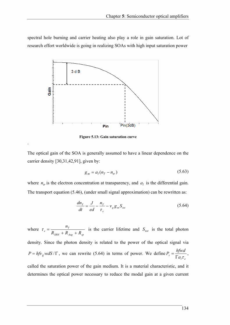
Chapter 5: Semiconductor optical amplifiers
134
spectral hole burning and carrier heating also play a role in gain saturation. Lot of
research effort worldwide is going in realizing SOAs with high input saturation power
.
The optical gain of the SOA is generally assumed to have a linear dependence on the
carrier density [30,31,42,91], given by:
)( trTlm nnag (5.63)
where trn is the electron concentration at transparency, and la is the differential gain.
The transport equation (5.46), (under small signal approximation) can be rewritten as:
totmge
TT Sgvn
ed
J
dt
dn
(5.64)
where spAugSRH
Te RRR
n
is the carrier lifetime and totS is the total photon
density. Since the photon density is related to the power of the optical signal via
/wdShfvP g , we can rewrite (5.64) in terms of power. We defineel
s a
hfwdP
,
called the saturation power of the gain medium. It is a material characteristic, and it
determines the optical power necessary to reduce the modal gain at a given current
Figure 5.13: Gain saturation curve
Chapter 5: Semiconductor optical amplifiers
135
density by 3 dB [4]. Using (5.63) and (5.64) we can solve for Tn under steady state
conditions:
s
tr
s
eT PP
Pn
P
P
ed
Jn
1
(5.65)
Substituting (5.63) and (5.65) in the amplifier equation (5.53) modifies it to:
sPP
Pg
dz
dP
/10
(5.66)
where
tr
el n
ed
Jag
0 is the unsaturated material gain. For simplicity we have
assumed 0 . The above equation can be solved, employing the boundary
conditions inPzP )0( and outPLzP )( , where L is the length of the amplifier,
we get:
s
in
P
PGGG )1(exp0 (5.67)
where inout PPG / is the amplifier gain, and LgG 00 exp is the unsaturated gain
of the amplifier. From (5.67) we can see that as when sin PP the exponential term
is almost 1, and the amplifier gain is 0G . However, when sin PP the gain
experiences a decrease. We can use (5.67) to estimate the saturation input power:
2
2ln2
0
G
PP ssat
in (5.68)
This leads to an expression for the output saturation power:
2
2ln2
0
0
G
GPP ssat
out (5.69)
For high amplifier gain, the output saturation power will be almost independent of the
unsaturated amplifier gain 0G .
Chapter 5: Semiconductor optical amplifiers
136
5.3.6 Gain recovery
When a high power, short optical pulse is injected into an SOA, the gain of the
amplifier reduces due to the reduction in carriers caused by the strong stimulated
recombinations induced by the optical signal. The depleted carriers are restored to the
steady state values via two processes [136]. First, a fast process (~ few ps) determined
by the spectral hole burning and carrier heating mechanisms. Second a slow process
determined by the filling of depleted carriers via the injected current. Since gain is
coupled with carrier density, these effects can be observed in the temporal evolution
of gain as well. Generally, the gain recovery is defined in terms of 10-90% recovery
time rect . It is the time needed for the amplifier gain ( LgmeG ) to rise from 10% to
90% of the saturation. Assuming only slow recovery processes, we can rewrite the
transport equation as
eff
TT n
ed
J
dt
dn
(5.70)
where SigASEspAugSRH
Teff RRRRR
n
is the effective carrier lifetime, also
referred as stimulated carrier lifetime in literature [94,139]. From (5.53) and (5.69) we
can find the dependence of optical gain on time:
eff
TT n
ed
J
dt
dn
(5.71)
From (5.71) it is possible to determine the 10-90% recovery in the optical gain
(assuming linear dependence of gain on carrier density Eq. (5.63)), let us call it rec , if
10% recovered gain is 1g and 90% recovered gain is 2g , then rec can be expressed
as:
s
seffrec gg
gg
2
1ln (5.72)
Thus the optical gain recovery depends on the effective carrier lifetime eff . Since the
amplifier gain depends on the optical gain ( LgmeG ), the gain recovery of the
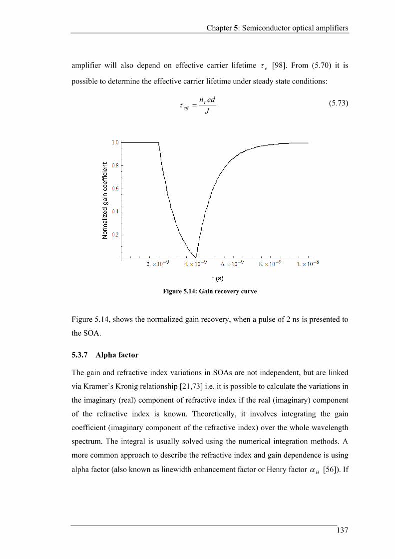
Chapter 5: Semiconductor optical amplifiers
137
amplifier will also depend on effective carrier lifetime e [98]. From (5.70) it is
possible to determine the effective carrier lifetime under steady state conditions:
J
ednTeff (5.73)
Figure 5.14, shows the normalized gain recovery, when a pulse of 2 ns is presented to
the SOA.
5.3.7 Alpha factor
The gain and refractive index variations in SOAs are not independent, but are linked
via Kramer’s Kronig relationship [21,73] i.e. it is possible to calculate the variations in
the imaginary (real) component of refractive index if the real (imaginary) component
of the refractive index is known. Theoretically, it involves integrating the gain
coefficient (imaginary component of the refractive index) over the whole wavelength
spectrum. The integral is usually solved using the numerical integration methods. A
more common approach to describe the refractive index and gain dependence is using
alpha factor (also known as linewidth enhancement factor or Henry factor H [56]). If
Figure 5.14: Gain recovery curve
Chapter 5: Semiconductor optical amplifiers
138
is the wavelength in free space, rn is the real part of the refractive index, mg is the
material gain, and Tn is the carrier density, then the alpha factor H is defined as:
Tm
TrH ng
nn
4
(5.74)
The alpha factor depends on the wavelength, current density and the semiconductor
material used for SOA. Most researchers assume H of an SOA to be constant
[56,85], however, this simplification is valid only for limited spectral range and for
small carrier density changes [136]. There exist various methods to directly measure
the alpha factor [86].
The alpha factor describes the fundamental linewidth enhancement of modes in
semiconductor lasers [56]. In semiconductor lasers the linewidth broadening is due to
fluctuations in the phase of the optical field. Two factors are responsible for this:
a) One the instantaneous fluctuations caused by each spontaneous photon emission.
b) Second, each emitted photon changes the emitted power, which in turn changes
gain and carrier density, resulting in delayed phase change. Besides affecting the
linewidth, it is a key parameter for high-speed modulation and high-power ap-
plications. When an optical signal propagates through a SOA it causes change in the
carrier density and thus changes the modal effective index and hence the propagation
coefficient. As a result, the leading edge of the optical pulse experiences a different
phase shift relative to the lagging edge of the optical pulse. This is self phase
modulation (SPM). The presence of SPM will cause change in both shape and
spectrum (chirp) of the optical signal. Long haul optical communication links employ
dispersion compensators based on SPM.
If more than one optical signal is present, there will be cross phase modulation (XPM)
between the signals, i.e. the refractive index changes due to the presence of optical
signal at one wavelength affects the output phase of optical signal at another
wavelength. XPM can be used to create wavelength converters, phase modulation and
all optical switches.
For semiconductor lasers and amplifiers small alpha factors are required to keep
chirping small, since the chirp causes signal degradation and limits modulation speed
Chapter 5: Semiconductor optical amplifiers
139
and transmission distances in optical communication systems. Furthermore small
alpha factors permit smaller linewidths, which allow to transmit more signal channels
within a given spectrum. In contrast for optical signal processing applications based
on self phase modulation (SPM) and cross phase modulation (XPM) high alpha-factor
are advantageous [77].
In [136] authors demonstrated that α-factor also has time dependence. The
dependence was attributed to several physical effects viz.: band filling, carrier heating
(CH), spectral hole burning (SHB), and two photon absorption (TPA).
5.4 Summary
This chapter starts with the review of semiconductor physics with a special focus on
the various generation and recombination processes. The coupled differential
equations describing the rate of change of photon density and carrier density were
described.
The chapter ends with a review of the Connelly model for modeling the steady state
gain characteristics of SOAs.

Chapter 6: Semiconductor optical amplifiers: Modeling using ATLAS
141
6 Semiconductor optical amplifiers: Modeling using ATLAS
6.1 ATLAS: An introduction
Several models have been developed in the past to simulate SOAs [23,30,31,62,81],
depending on the behavior we want to simulate, one model can be better than others.
In general, they all solve rate equations, i.e., time dependent differential equations for
the carrier and photons, and either, average the carrier density over the entire length of
the device or segment the SOA into small segments. In Section 5.3.4 we presented a
widely used steady state model for SOAs the Connelly Model. However, they all are
able to give a reasonable approximation of the SOA behavior in the prescribed region
of operation; they do not provide insight into the actual physics taking place inside the
device. In order to get a better physical insight, here we use ATLAS, a simulation tool
developed by Silvaco to predict the saturation properties and alpha factor of bulk
SOA.
ATLAS is a device simulation tool which takes into account all the physical
phenomenon and the complete device structure. ATLAS enables device technology
engineers to simulate the electrical, optical, and thermal behavior of semiconductor
devices. ATLAS provides a physics-based, easy to use, modular, and extensible
Chapter 6: Semiconductor optical amplifiers: Modeling using ATLAS
142
platform to characterize semiconductor based technologies. Such a device simulation
predicts the electrical and optical characteristics that are associated with specific
physical structures and bias conditions. The physics based simulation of devices
provides three advantages, i.e., it is predictive, it provides insight and it captures
theoretical knowledge in a manner that makes this knowledge available to non-experts
[10,133]. Physics based simulation is different from empirical modeling. In empirical
modeling, one obtains analytic formulae that approximate the existing data with good
accuracy and minimum complexity. It does not usually provide insight, or predictive
capabilities or encapsulation of theoretical knowledge. Physics based simulation is an
alternative to experiments as a source of data and has become important for two major
reasons: firstly, it is cheaper and quicker than performing experiments, and secondly,
it provides information that is difficult or impossible to measure.
The drawbacks with such simulation are that all relevant physics must be incorporated
into a simulator, and numerical procedures must be implemented to solve the
associated equations. For example in ATLAS to simulate any device, one needs to
define the following [10]:
1. Physical structure to be simulated.
2. Physical models to be used.
3. Bias conditions for which electrical characteristics are to be simulated.
6.2 Simulation model and material parameters
The first step in modeling a structure using ATLAS is to determine the material
parameters and decide the electric and optic models to be used. We have simulated
SOAs based on the InP/InGaAsP material system. Table 6-1 lists the material
parameters used in our simulation. The MATERIAL statement is used to specify
material parameters for each material constituting the SOA.
The next step is to decide on the models necessary to simulate all the physics
important for our simulation. We want to include Auger recombination, Shockley
Read and Hall recombination as non radiative recombinations, and spontaneous
radiative recombination. Also, the electrons and holes follow Fermi distribution. And
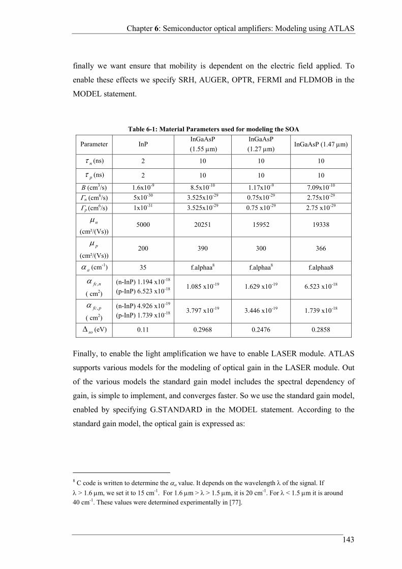
Chapter 6: Semiconductor optical amplifiers: Modeling using ATLAS
143
finally we want ensure that mobility is dependent on the electric field applied. To
enable these effects we specify SRH, AUGER, OPTR, FERMI and FLDMOB in the
MODEL statement.
Table 6-1: Material Parameters used for modeling the SOA
Parameter InP InGaAsP
(1.55 m)
InGaAsP
(1.27 m) InGaAsP (1.47 m)
n (ns) 2 10 10 10
p (ns) 2 10 10 10
B (cm3/s) 1.6x10⁻⁹ 8.5x10⁻¹⁰ 1.17x10⁻⁹ 7.09x10⁻¹⁰
n (cm6/s) 5x10-30 3.525x10⁻²⁹ 0.75x10⁻²⁹ 2.75x10⁻²⁹
p (cm6/s) 1x10-31 3.525x10⁻²⁹ 0.75 x10⁻²⁹ 2.75 x10⁻²⁹
n
(cm²/(Vs)) 5000 20251 15952 19338
p
(cm²/(Vs)) 200 390 300 366
a (cm-1) 35 f.alphaa8 f.alphaa8 f.alphaa8
nfc ,
( cm2)
(n-InP) 1.194 x10⁻¹⁸ (p-InP) 6.523 x10⁻¹⁸
1.085 x10⁻¹⁹ 1.629 x10⁻¹⁹ 6.523 x10⁻¹⁸
pfc,
( cm2)
(n-InP) 4.926 x10⁻¹⁹ (p-InP) 1.739 x10⁻¹⁸
3.797 x10⁻¹⁹ 3.446 x10⁻¹⁹ 1.739 x10⁻¹⁸
so (eV) 0.11 0.2968 0.2476 0.2858
Finally, to enable the light amplification we have to enable LASER module. ATLAS
supports various models for the modeling of optical gain in the LASER module. Out
of the various models the standard gain model includes the spectral dependency of
gain, is simple to implement, and converges faster. So we use the standard gain model,
enabled by specifying G.STANDARD in the MODEL statement. According to the
standard gain model, the optical gain is expressed as:
8 C code is written to determine the a value. It depends on the wavelength of the signal. If
> 1.6 m, we set it to 15 cm-1. For 1.6 m > > 1.5 m, it is 20 cm-1. For < 1.5 m it is around
40 cm-1. These values were determined experimentally in [77].
Chapter 6: Semiconductor optical amplifiers: Modeling using ATLAS
144
)()(0 hvecB
gm WfWf
Tk
WhfGainfg
(6.1)
where Gain0 is a user defined parameter. Comparing equations (5.39) and (6.1) we obtain the expression for Gain0 as:
Tkm
nn
cGain B
r
spg33
2/3
2
2
0 82
(6.2)
While, optical gain results in an increase in the photon density, there are various loss
mechanisms causing decrease in the photon density. These losses are activated in the
LASER module by using flags FCARRIER for free carrier absorption loss,
ABSORPTION for bulk absorption loss. Since the SOA is essentially a laser with no
facet mirrors, the mirror reflectivities are set to 0.0001 using the MIRROR parameter
in LASER statement. To include a Lorentzian spectral broadening, we specified
LORENTZ in the LASER statement.
Amplified spontaneous emission is an important process in LASER/SOAs. In Section
6.3.1 we discuss the model used to include ASE
6.3 ATLAS simulation: issues to be resolved
ATLAS is a versatile simulation tool with the capability to include various physical
effects important for semiconductor lasers. An SOA is essentially a semiconductor
laser with low mirror reflectivities [30,31,42,91]. Thus, theoretically speaking by
reducing the mirror reflectivities in ATLAS LASER module, we should be able to
model an SOA. This can provide us with the information regarding gain and ASE
spectrum of the SOA under no signal conditions. However, this information is
insufficient. An SOA as an amplifier or optical signal processor operates on an input
optical signal. For complete characterization of an SOA it is important to know how
the gain and carrier densities of the amplifier change (gain saturation and gain
recovery) in response to the optical signal. Unfortunately, ATLAS has no support for
an optical input to an SOA. This made us to improvise, from the existing models in
ATLAS, a way that will have the similar effect on carriers and gain as an input optical
signal have. We choose to change the radiative recombination parameter B for
implementing the effect of an optical source on the carrier numbers. Here we should
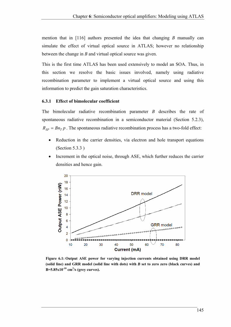
Chapter 6: Semiconductor optical amplifiers: Modeling using ATLAS
145
mention that in [116] authors presented the idea that changing B manually can
simulate the effect of virtual optical source in ATLAS; however no relationship
between the change in B and virtual optical source was given.
This is the first time ATLAS has been used extensively to model an SOA. Thus, in
this section we resolve the basic issues involved, namely using radiative
recombination parameter to implement a virtual optical source and using this
information to predict the gain saturation characteristics.
6.3.1 Effect of bimolecular coefficient
The bimolecular radiative recombination parameter B describes the rate of
spontaneous radiative recombination in a semiconductor material (Section 5.2.3),
pBnR TSP . The spontaneous radiative recombination process has a two-fold effect:
Reduction in the carrier densities, via electron and hole transport equations
(Section 5.3.3 )
Increment in the optical noise, through ASE, which further reduces the carrier
densities and hence gain.
Figure 6.1: Output ASE power for varying injection currents obtained using DRR model
(solid line) and GRR model (solid line with dots) with B set to zero zero (black curves) and
B=5.85x10⁻¹⁰ cm3/s (grey curves).
Chapter 6: Semiconductor optical amplifiers: Modeling using ATLAS
146
The presence of an optical input signal results in reduction of the carrier densities by
the process of stimulated emission. It has no direct effect on ASE. We want to model
the effect of the presence of an optical signal by making manual changes in the
parameter B. This necessitates that as we change B, it reduces the carrier density, but
has no direct effect on the ASE.
To account for the radiative recombination in the transport equation, we set the logical
parameter OPTR to true value. For ASE, ATLAS has two mutually exclusive
models [10]:
1. General radiative recombination model (GRR): The general radiative model is
enabled by specifying ^SPONTANEOS in the LASER statement. In this
model the ASE has no spectral dependence.
2. Default radiative recombination model (DRR): This model is set by default in
LASER. In this model the ASE has spectral dependence.
In order to ascertain which model for the ASE fulfills our criteria, we compare the
output ASE power and the material gain coefficient as obtained from the two models
for two different values of radiative recombination parameter B. Figure 6.1 shows the
output ASE power of the SOA (Section 5.3.2 ) for the two mutually exclusive ASE
models, with B set to zero and B set to non zero value. As expected, for the GRR
model there is no output ASE when B has a zero value. When B has a non zero value
the output power has direct dependence on the injection current (i.e. carrier density).
The DRR model, on the other hand, gives a higher non-zero output ASE power when
B is zero. For non-zero B the output ASE power decreases. This implies that in the
GRR model the ASE has a direct dependence on radiative recombination parameter B,
while in the DRR model the ASE is indirectly affected by B. The radiative
recombinations in the SOA decrease the carrier density, and reduced carrier density
decreases ASE.
Figure 6.2 shows that the material gain for both models is same. This is so because the
material gain depends on the carrier concentration, and the ASE generated by DRR
model is too low to have any significant effect on the carrier concentration. Further in
both models the gain is higher for B set to zero. The reason for this is that when B is
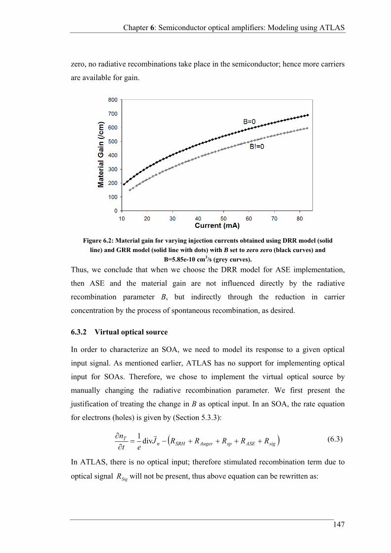
Chapter 6: Semiconductor optical amplifiers: Modeling using ATLAS
147
zero, no radiative recombinations take place in the semiconductor; hence more carriers
are available for gain.
Thus, we conclude that when we choose the DRR model for ASE implementation,
then ASE and the material gain are not influenced directly by the radiative
recombination parameter B, but indirectly through the reduction in carrier
concentration by the process of spontaneous recombination, as desired.
6.3.2 Virtual optical source
In order to characterize an SOA, we need to model its response to a given optical
input signal. As mentioned earlier, ATLAS has no support for implementing optical
input for SOAs. Therefore, we chose to implement the virtual optical source by
manually changing the radiative recombination parameter. We first present the
justification of treating the change in B as optical input. In an SOA, the rate equation
for electrons (holes) is given by (Section 5.3.3):
sigASEspAugerSRHnT RRRRRJ
et
n
div1
(6.3)
In ATLAS, there is no optical input; therefore stimulated recombination term due to
optical signal SigR will not be present, thus above equation can be rewritten as:
Figure 6.2: Material gain for varying injection currents obtained using DRR model (solid
line) and GRR model (solid line with dots) with B set to zero zero (black curves) and
B=5.85e-10 cm3/s (grey curves).
Chapter 6: Semiconductor optical amplifiers: Modeling using ATLAS
148
ASEspAugerSRHnT RRRRJ
et
n
div1
(6.4)
Here pBnR Tsp corresponds to the recombination rate due to spontaneous emission.
If we manually change the radiative recombination parameter from B to BB , then
we have
pBnRpBnRRJet
nTASETAugerSRHn
T
div1
(6.5)
Thus, increase in the radiative recombination parameter from B to BB results in a
reduction of the carrier density in a similar fashion as for an optical signal. Hence, we
are justified in implementing a virtual optical source by manual change in B.
Comparing (6.3) with (6.5), we get that:
pBnR Tsig (6.6)
Let us consider a small section l of the amplifying medium; for a small section, the
recombination rate sigR depends directly on the photon density sigS (unit 3cm ):
sigmsig SlgR (6.7)
The power is related with photon density by relation: SAlhfP eff , where effA is the
effective area interacting with optical field. Thus, we obtain the power at the input by
relation
lgsigin
mewd
SlhfP
(6.8)
The exponential term takes into account that the photons have undergone
amplification within the amplifying medium. Combining (6.6) to (6.8), we get an
expression for the input signal in terms of the change in the radiative recombination
parameter B , saturated electron and hole concentration, and the reduced material
gain mg
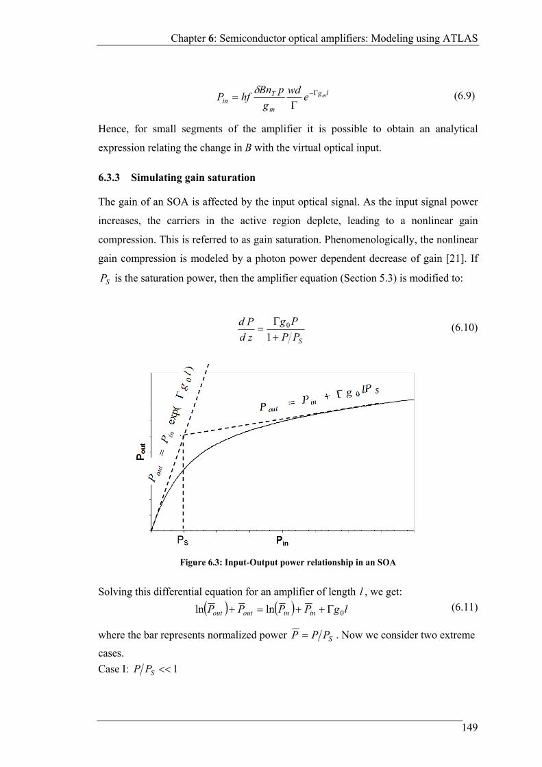
Chapter 6: Semiconductor optical amplifiers: Modeling using ATLAS
149
lg
m
Tin
mewd
g
pBnhfP
(6.9)
Hence, for small segments of the amplifier it is possible to obtain an analytical
expression relating the change in B with the virtual optical input.
6.3.3 Simulating gain saturation
The gain of an SOA is affected by the input optical signal. As the input signal power
increases, the carriers in the active region deplete, leading to a nonlinear gain
compression. This is referred to as gain saturation. Phenomenologically, the nonlinear
gain compression is modeled by a photon power dependent decrease of gain [21]. If
SP is the saturation power, then the amplifier equation (Section 5.3) is modified to:
SPP
Pg
zd
Pd
1
0 (6.10)
Solving this differential equation for an amplifier of length l , we get:
lgPPPP ininoutout 0lnln (6.11)
where the bar represents normalized power SPPP . Now we consider two extreme
cases.
Case I: 1SPP
Figure 6.3: Input-Output power relationship in an SOA
Chapter 6: Semiconductor optical amplifiers: Modeling using ATLAS
150
In these circumstances, the logarithmic terms in (6.11) dominate, resulting in:
lgPP inout 0lnln lgPP inout 0exp (6.12)
This represents the equation of a linear amplifier.
Case II: 1SPP
In these circumstances, the linear terms in (6.11) dominate, resulting in:
lgPP inout 0 Sinout PlgPP 0 (6.13)
This represents the equation of a saturated amplifier.
Figure 6.3 represents the two cases. There exists a linear relationship between input
and output. For a small amplifier segment, the intersection of these two curves
represents the saturation power SP . Thus if we are able to obtain the two linear
relation, we can get an estimate of the saturation power of the amplifier.
6.4 Simulation results
We considered two SOA structures for simulation. The first is a ridge waveguide SOA
(Figure 6.4) [77], the second is a buried hetrostructure (Figure 6.5). Both SOAs are
based on InGaAsP/InP material system. This material system provides optical gain in
μm3.1 to μm6.1 wavelength range, making them suitable for fiber optic
transmission system. Our simulation takes into account all the physical effects
described in Section 5.2. ATLAS allows the selection of different physical effects
with the help of logical parameters in the MODEL statement [10].
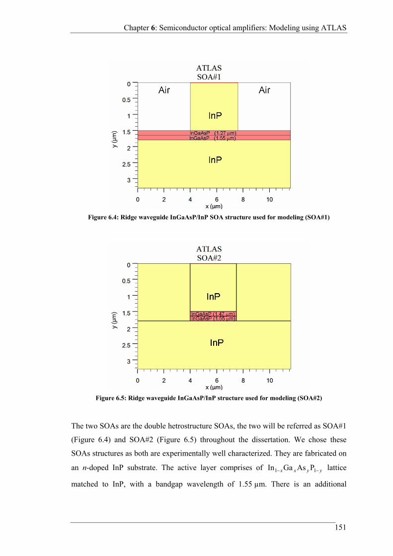
Chapter 6: Semiconductor optical amplifiers: Modeling using ATLAS
151
The two SOAs are the double hetrostructure SOAs, the two will be referred as SOA#1
(Figure 6.4) and SOA#2 (Figure 6.5) throughout the dissertation. We chose these
SOAs structures as both are experimentally well characterized. They are fabricated on
an n-doped InP substrate. The active layer comprises of yyxx 11 PAsGaIn lattice
matched to InP, with a bandgap wavelength of 1.55 µm. There is an additional
Figure 6.4: Ridge waveguide InGaAsP/InP SOA structure used for modeling (SOA#1)
Figure 6.5: Ridge waveguide InGaAsP/InP structure used for modeling (SOA#2)
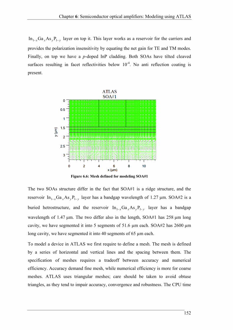
Chapter 6: Semiconductor optical amplifiers: Modeling using ATLAS
152
yyxx 11 PAsGaIn layer on top it. This layer works as a reservoir for the carriers and
provides the polarization insensitivity by equating the net gain for TE and TM modes.
Finally, on top we have a p-doped InP cladding. Both SOAs have tilted cleaved
surfaces resulting in facet reflectivities below 10-4. No anti reflection coating is
present.
The two SOAs structure differ in the fact that SOA#1 is a ridge structure, and the
reservoir yyxx 11 PAsGaIn layer has a bandgap wavelength of 1.27 µm. SOA#2 is a
buried hetrostructure, and the reservoir yyxx 11 PAsGaIn layer has a bandgap
wavelength of 1.47 µm. The two differ also in the length, SOA#1 has 258 µm long
cavity, we have segmented it into 5 segments of 51.6 µm each. SOA#2 has 2600 µm
long cavity, we have segmented it into 40 segments of 65 µm each.
To model a device in ATLAS we first require to define a mesh. The mesh is defined
by a series of horizontal and vertical lines and the spacing between them. The
specification of meshes requires a tradeoff between accuracy and numerical
efficiency. Accuracy demand fine mesh, while numerical efficiency is more for coarse
meshes. ATLAS uses triangular meshes; care should be taken to avoid obtuse
triangles, as they tend to impair accuracy, convergence and robustness. The CPU time
Figure 6.6: Mesh defined for modeling SOA#1
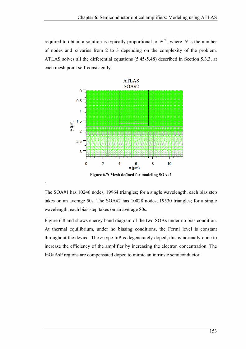
Chapter 6: Semiconductor optical amplifiers: Modeling using ATLAS
153
required to obtain a solution is typically proportional to N , where N is the number
of nodes and varies from 2 to 3 depending on the complexity of the problem.
ATLAS solves all the differential equations (5.45-5.48) described in Section 5.3.3, at
each mesh point self-consistently
.
The SOA#1 has 10246 nodes, 19964 triangles; for a single wavelength, each bias step
takes on an average 50s. The SOA#2 has 10028 nodes, 19530 triangles; for a single
wavelength, each bias step takes on an average 80s.
Figure 6.8 and shows energy band diagram of the two SOAs under no bias condition.
At thermal equilibrium, under no biasing conditions, the Fermi level is constant
throughout the device. The n-type InP is degenerately doped; this is normally done to
increase the efficiency of the amplifier by increasing the electron concentration. The
InGaAsP regions are compensated doped to mimic an intrinsic semiconductor.
Figure 6.7: Mesh defined for modeling SOA#2
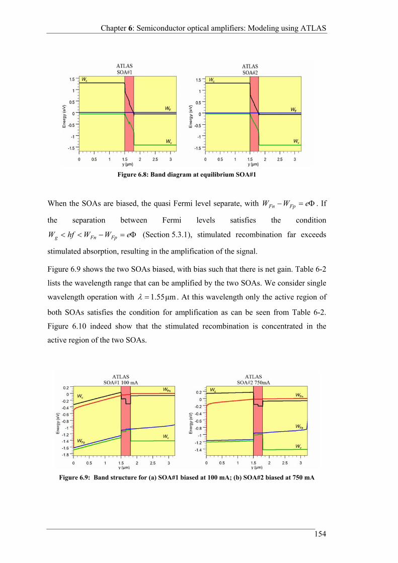
Chapter 6: Semiconductor optical amplifiers: Modeling using ATLAS
154
When the SOAs are biased, the quasi Fermi level separate, with eWW FpFn . If
the separation between Fermi levels satisfies the condition
eWWhfW FpFng (Section 5.3.1), stimulated recombination far exceeds
stimulated absorption, resulting in the amplification of the signal.
Figure 6.9 shows the two SOAs biased, with bias such that there is net gain. Table 6-2
lists the wavelength range that can be amplified by the two SOAs. We consider single
wavelength operation with μm55.1 . At this wavelength only the active region of
both SOAs satisfies the condition for amplification as can be seen from Table 6-2.
Figure 6.10 indeed show that the stimulated recombination is concentrated in the
active region of the two SOAs.
Figure 6.8: Band diagram at equilibrium SOA#1
Figure 6.9: Band structure for (a) SOA#1 biased at 100 mA; (b) SOA#2 biased at 750 mA

Chapter 6: Semiconductor optical amplifiers: Modeling using ATLAS
155
Table 6-2: Bandgap, Fermi level separation and the corresponding range of optical wavelengths
that can be amplified
SOA#1 biased at an injection current of 100 mA
Region )eV(gW )eV(FpFn WW
Amplification
range )μm(
Active Region 0.783 1.03 58.121.1
Reservoir 0.98 1.05 27.118.1
SOA#2 biased at an injection current of 750 mA
Active Region 0.786 0.94 58.132.1
Reservoir 0.852 0.937 45.132.1
shows the intensity distribution of the fundamental transverse mode in the two SOAs.
For SOA#1 the mode is strongly confined under the ridge of the waveguide. For
SOA#2, the mode is confined in the active region, as expected.
Figure 6.10: Stimulated recombination rate for SOA#1 biased at 100 mA
(a) (b)
Figure 6.11: Mode profile (a) SOA#1 at 100 mA; (b) SOA#2 at 750 mA
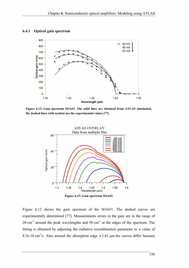
Chapter 6: Semiconductor optical amplifiers: Modeling using ATLAS
156
6.4.1 Optical gain spectrum
Figure 6.12 shows the gain spectrum of the SOA#1. The dashed curves are
experimentally determined [77]. Measurements errors in the gain are in the range of
20 cm-1 around the peak wavelengths and 50 cm-1 at the edges of the spectrum. The
fitting is obtained by adjusting the radiative recombination parameter to a value of
8.5e-10 cm3/s. Also around the absorption edge μm61.1 the curves differ because
Figure 6.12: Gain spectrum SOA#1. The solid lines are obtained from ATLAS simulation,
the dashed lines with symbol are the experimental values [77].
Figure 6.13: Gain spectrum SOA#2
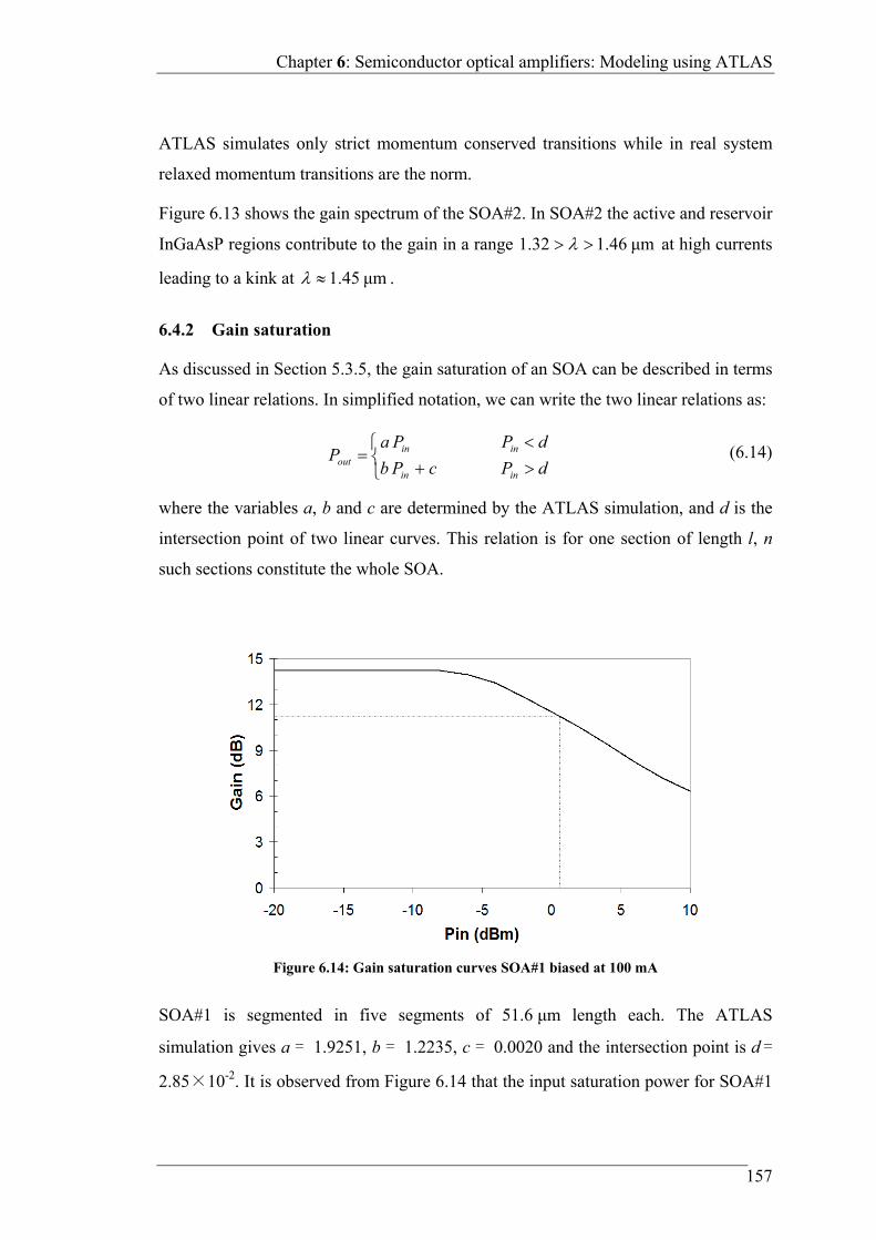
Chapter 6: Semiconductor optical amplifiers: Modeling using ATLAS
157
ATLAS simulates only strict momentum conserved transitions while in real system
relaxed momentum transitions are the norm.
Figure 6.13 shows the gain spectrum of the SOA#2. In SOA#2 the active and reservoir
InGaAsP regions contribute to the gain in a range μm46.132.1 at high currents
leading to a kink at μm45.1 .
6.4.2 Gain saturation
As discussed in Section 5.3.5, the gain saturation of an SOA can be described in terms
of two linear relations. In simplified notation, we can write the two linear relations as:
dPcPb
dPPaP
inin
ininout (6.14)
where the variables a, b and c are determined by the ATLAS simulation, and d is the
intersection point of two linear curves. This relation is for one section of length l, n
such sections constitute the whole SOA.
SOA#1 is segmented in five segments of 51.6 μm length each. The ATLAS
simulation gives a = 1.9251, b = 1.2235, c = 0.0020 and the intersection point is d =
2.85×10⁻². It is observed from Figure 6.14 that the input saturation power for SOA#1
Figure 6.14: Gain saturation curves SOA#1 biased at 100 mA

Chapter 6: Semiconductor optical amplifiers: Modeling using ATLAS
158
biased at 100 mA is 0.6 dBm. The expression for gain saturation developed in Section
5.3.5, gives the input saturation power for same biasing conditions as 0.73 dBm. This
justifies the use of expression of Eq. (5.68) to estimate input saturation power.
SOA#2 is segmented in 40 sections of 65 μm length each. For SOA#2 biased at
300 mA, the variables are a=1.1288, b=1.0616, c=0.0009 and the intersection point is
d)=0.00391. Figure 6.15 shows the gain saturation curve for SOA#2, the curve
obtained using ATLAS simulation matches well with the experimental data.
9The measurements for SOA#2 were done by Andrej Marculescu at the Institute of Photonics and Quantum Electronics, University of Karlsruhe, Germany. The experimental setup is given in Appendix D
Figure 6.15: Gain saturation curves for SOA#2 biased at 300 mA . The Solid line is obtained
from ATLAS simulation, the dashed line with symbol is obtained experimentally9
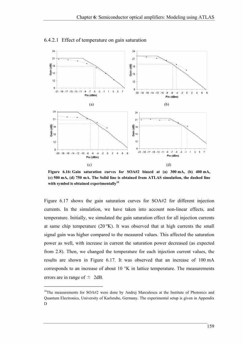
Chapter 6: Semiconductor optical amplifiers: Modeling using ATLAS
159
6.4.2.1 Effect of temperature on gain saturation
Figure 6.17 shows the gain saturation curves for SOA#2 for different injection
currents. In the simulation, we have taken into account non-linear effects, and
temperature. Initially, we simulated the gain saturation effect for all injection currents
at same chip temperature (20 ºK). It was observed that at high currents the small
signal gain was higher compared to the measured values. This affected the saturation
power as well, with increase in current the saturation power decreased (as expected
from 2.8). Then, we changed the temperature for each injection current values, the
results are shown in Figure 6.17. It was observed that an increase of 100 mA
corresponds to an increase of about 10 °K in lattice temperature. The measurements
errors are in range of ± 2dB.
10The measurements for SOA#2 were done by Andrej Marculescu at the Institute of Photonics and Quantum Electronics, University of Karlsruhe, Germany. The experimental setup is given in Appendix D
(a) (b)
(c) (d)
Figure 6.16: Gain saturation curves for SOA#2 biased at (a) 300 mA, (b) 400 mA,
(c) 500 mA, (d) 750 mA. The Solid line is obtained from ATLAS simulation, the dashed line
with symbol is obtained experimentally10
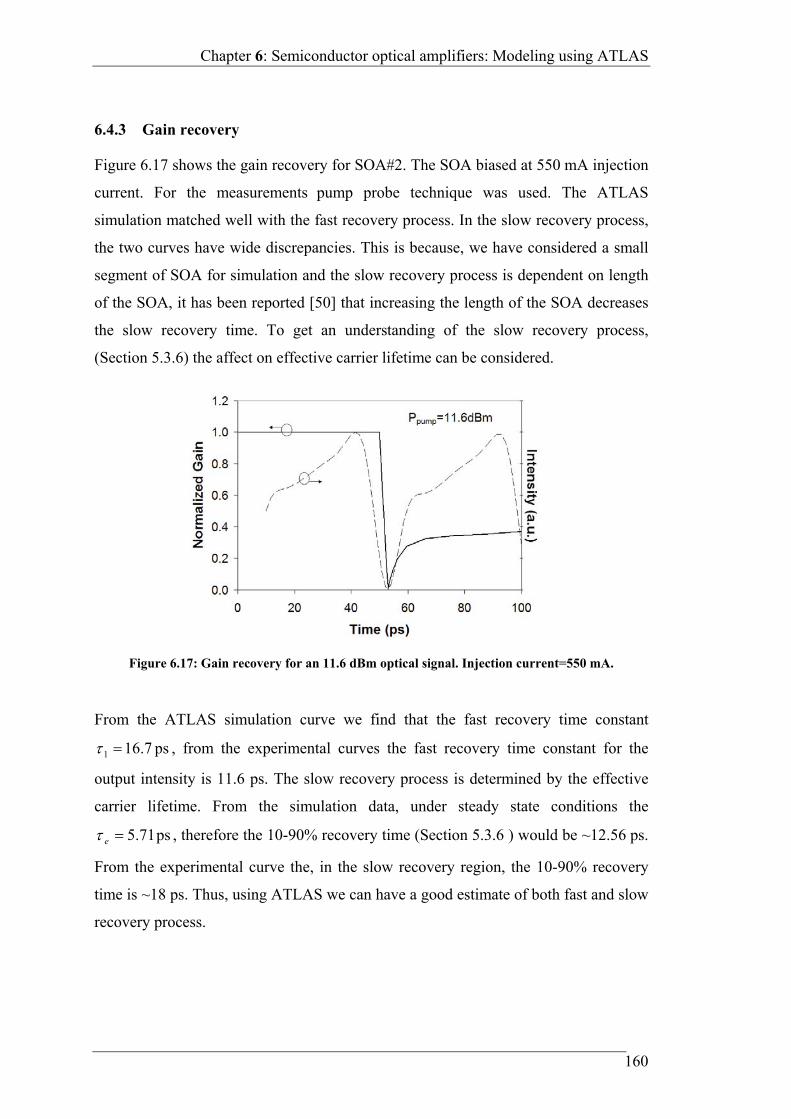
Chapter 6: Semiconductor optical amplifiers: Modeling using ATLAS
160
6.4.3 Gain recovery
Figure 6.17 shows the gain recovery for SOA#2. The SOA biased at 550 mA injection
current. For the measurements pump probe technique was used. The ATLAS
simulation matched well with the fast recovery process. In the slow recovery process,
the two curves have wide discrepancies. This is because, we have considered a small
segment of SOA for simulation and the slow recovery process is dependent on length
of the SOA, it has been reported [50] that increasing the length of the SOA decreases
the slow recovery time. To get an understanding of the slow recovery process,
(Section 5.3.6) the affect on effective carrier lifetime can be considered.
From the ATLAS simulation curve we find that the fast recovery time constant
ps7.161 , from the experimental curves the fast recovery time constant for the
output intensity is 11.6 ps. The slow recovery process is determined by the effective
carrier lifetime. From the simulation data, under steady state conditions the
ps71.5e , therefore the 10-90% recovery time (Section 5.3.6 ) would be ~12.56 ps.
From the experimental curve the, in the slow recovery region, the 10-90% recovery
time is ~18 ps. Thus, using ATLAS we can have a good estimate of both fast and slow
recovery process.
Figure 6.17: Gain recovery for an 11.6 dBm optical signal. Injection current=550 mA.
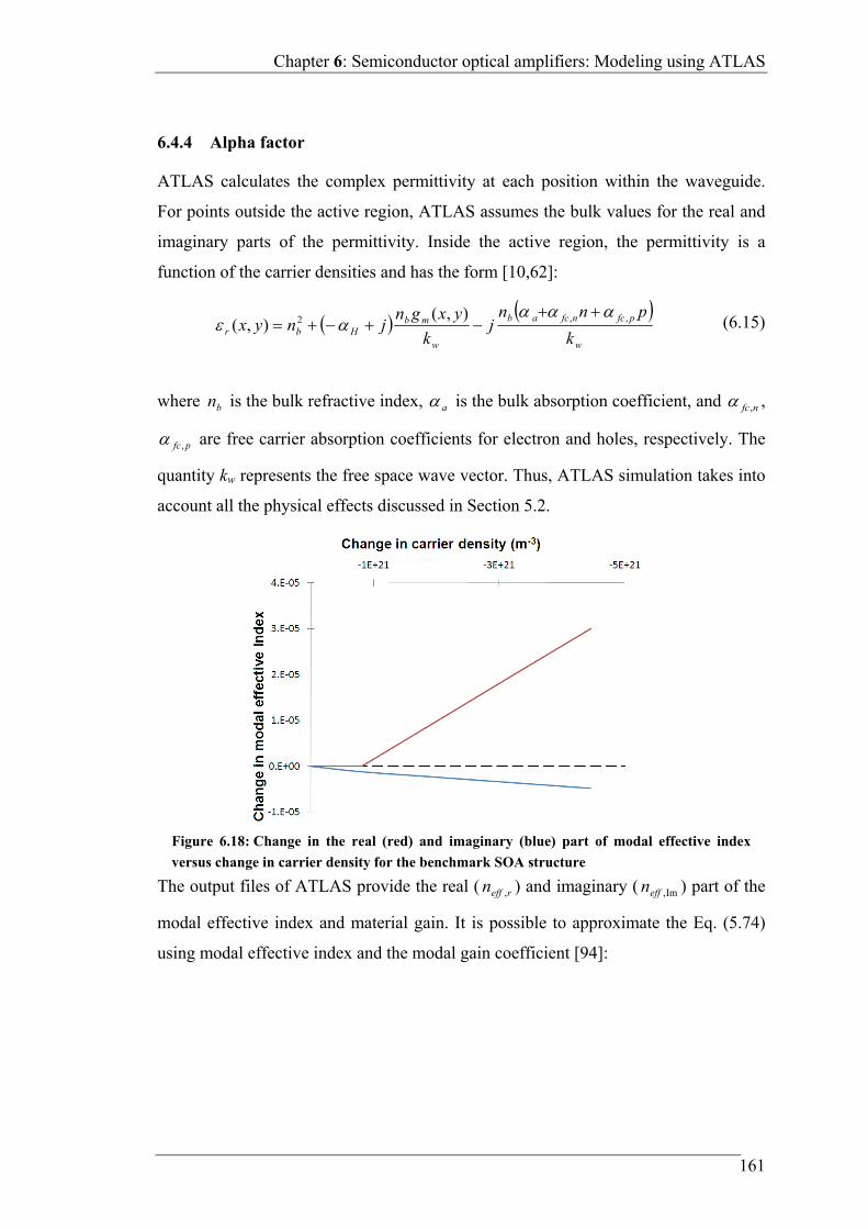
Chapter 6: Semiconductor optical amplifiers: Modeling using ATLAS
161
6.4.4 Alpha factor
ATLAS calculates the complex permittivity at each position within the waveguide.
For points outside the active region, ATLAS assumes the bulk values for the real and
imaginary parts of the permittivity. Inside the active region, the permittivity is a
function of the carrier densities and has the form [10,62]:
w
pfcnfcab
w
mbHbr k
pnnj
k
yxgnjnyx ,,2 ),(
),(
(6.15)
where bn is the bulk refractive index, a is the bulk absorption coefficient, and nfc, ,
pfc, are free carrier absorption coefficients for electron and holes, respectively. The
quantity kw represents the free space wave vector. Thus, ATLAS simulation takes into
account all the physical effects discussed in Section 5.2.
The output files of ATLAS provide the real ( reffn , ) and imaginary ( Im,effn ) part of the
modal effective index and material gain. It is possible to approximate the Eq. (5.74)
using modal effective index and the modal gain coefficient [94]:
Figure 6.18: Change in the real (red) and imaginary (blue) part of modal effective index
versus change in carrier density for the benchmark SOA structure
Chapter 6: Semiconductor optical amplifiers: Modeling using ATLAS
162
Tm
TreffH ng
nn
)(
4 ,
(6.16)
We make use of Eq. (6.16) for the alpha factor calculations. For the signal wavelength
of 1.55 m, at a biasing current of 100 mA the measured value [77] of alpha factor is
4.8 at a cavity temperature of C25 . From ATLAS simulations under the same
conditions the alpha factor is 8.4. This demonstrates that we are justified in using
ATLAS for simulating bulk SOA, and that we can further use ATLAS to predict the
behavior of modified bulk SOA.
6.5 Summary
In this chapter we investigated the use of Silvaco’s ATLAS to model SOA. The
simulation tool ATLAS supports simulation of semiconductor lasers only, however
making the mirror reflectivities small, the lasing threshold is increased such that lasers
are essentially reduced to amplifiers. Next, for investigating the saturation
characteristics of SOA, the amplifier gain should be influenced by injecting an optical
light power. However, ATLAS cannot simulate the required source directly. Instead,
we use in the electron rate equation simultaneously two competing independent
models for spontaneous radiative recombination, namely the so-called general model
(total recombination rate BnT p with bimolecular recombination coefficient B, electron
and hole concentrations nT and p) and the standard model for recombination due to
amplified spontaneous emission into the mode under consideration (determined by the
product of Fermi functions for electrons and holes). In the photon rate equation, only
the standard model is used. We then increase B, and thus simulate a decrease of the
carrier concentration that would physically result from an external optical signal.
We chose an experimentally well-characterized structure for our physically-based
simulations [77] with the ATLAS package, and thus were able to check reference
simulations with measurements.
This work in parts has been reported in the following Publications:

Chapter 6: Semiconductor optical amplifiers: Modeling using ATLAS
163
Amita Kapoor, E. K Sharma, W. Freude and J. Leuthold, Saturation
Characteristics of InGaAsP-InP bulk SOA, Proc. of SPIE 7597, 75971I,
(2010).

Chapter 7: Engineering bulk semiconductor optical amplifiers
165
7 Engineering bulk semiconductor optical amplifiers
7.1 Gain saturation
The gain saturation and gain recovery behavior of an SOA is important not only for
SOA as a linear amplifier but also for other signal processing tasks. Depending on the
specific task, the design of an SOA is modified to optimize the performance. For
example, for an SOA as a linear amplifier the requirements are high gain, high
saturation power and fast recovery. For SOA as wavelength converters the desired
properties are low saturation power and fast recovery.
From Section 5.3.5 the input and output saturation power of an SOA can be expressed
as:
2
2ln2
0
G
wd
a
hfP
el
satin
(7.1)
0GPP satin
satout (7.2)
From Eqs. (7.1) and (7.2) we see that the saturation power depends inversely upon the
carrier life time e , differential gain la and the saturation power is proportional to the
effective area /wd . The dependence of the saturation power on the unsaturated gain
Chapter 7: Engineering bulk semiconductor optical amplifiers
166
0G is slightly complex, while the input saturation power decreases with increase in
0G , for high gain the output saturation power is almost independent of 0G .
Researchers for last two decades have tried to influence all these parameters to
improve the saturation behavior of an SOA. Below we discuss the factors affecting
each of these parameters and how they have been employed to improve the saturation
behavior.
The differential gain la is a property of the gain material. The QW SOAs have been
reported to have high output saturation power (+19.6 dBm [90]) as compared to bulk
SOAs. This is so, because in QW SOAs, the modal gain is weakly dependent on the
injection current at high current densities, owing to the approximate logarithmic
dependence of material gain on current density [140]. As a result, gain is relatively
insensitive to the change in carrier densities [72], making it possible to achieve higher
saturation power in QW SOAs. The effective area /wd depends upon the active
layer width w , depth d and the confinement factor . In conventional SOAs, the gain
and efficiency considerations restrict the change in active layer depth, and the width is
constrained by the fact that increase in width can result in transverse multimode
propagation in the amplifying waveguide. However, the width can be smoothly and
gradually increased along the longitudinal axis to achieve wide cross-sections and
simultaneously keeping most of the power in the lowest order mode. Such amplifiers
are known as tapered SOAs [16,17,41]. Significant improvement in output saturation
power (~+28 dBm) has been reported by employing these structures [41]. Lastly, we
consider the effect of carrier lifetime eff . (For low signal condition effe ~ ) Decrease
in carrier lifetime increases the saturation power, at the same time from (5.72) we see
that the gain recovery of SOA is also directly dependent on the carrier lifetime. The
carrier lifetime eff itself depends on the applied current and the optical intensity in the
active layer. A high current provides a large current density and a high amplified
spontaneous emission, both of which tend to reduce the carrier lifetime. However, as
the current is increased, temperature effects can dominate leading to reduction in gain,
saturation power and gain recovery. In [98] it was claimed that both the saturation
output power and the gain recovery could be improved by using optical injection near
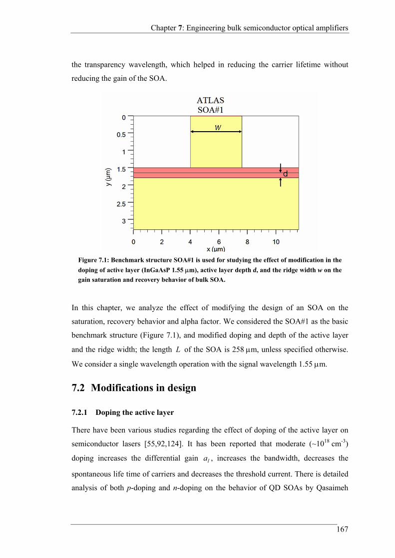
Chapter 7: Engineering bulk semiconductor optical amplifiers
167
the transparency wavelength, which helped in reducing the carrier lifetime without
reducing the gain of the SOA.
In this chapter, we analyze the effect of modifying the design of an SOA on the
saturation, recovery behavior and alpha factor. We considered the SOA#1 as the basic
benchmark structure (Figure 7.1), and modified doping and depth of the active layer
and the ridge width; the length L of the SOA is 258 m, unless specified otherwise.
We consider a single wavelength operation with the signal wavelength 1.55 m.
7.2 Modifications in design
7.2.1 Doping the active layer
There have been various studies regarding the effect of doping of the active layer on
semiconductor lasers [55,92,124]. It has been reported that moderate (~1018 cm-3)
doping increases the differential gain la , increases the bandwidth, decreases the
spontaneous life time of carriers and decreases the threshold current. There is detailed
analysis of both p-doping and n-doping on the behavior of QD SOAs by Qasaimeh
Figure 7.1: Benchmark structure SOA#1 is used for studying the effect of modification in the
doping of active layer (InGaAsP 1.55 m), active layer depth d, and the ridge width w on the
gain saturation and recovery behavior of bulk SOA.
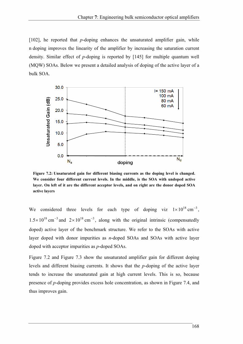
Chapter 7: Engineering bulk semiconductor optical amplifiers
168
[102], he reported that p-doping enhances the unsaturated amplifier gain, while
n doping improves the linearity of the amplifier by increasing the saturation current
density. Similar effect of p-doping is reported by [145] for multiple quantum well
(MQW) SOAs. Below we present a detailed analysis of doping of the active layer of a
bulk SOA.
We considered three levels for each type of doping viz 318 cm101 ,
318 cm105.1 and 318 cm102 , along with the original intrinsic (compensatedly
doped) active layer of the benchmark structure. We refer to the SOAs with active
layer doped with donor impurities as n-doped SOAs and SOAs with active layer
doped with acceptor impurities as p-doped SOAs.
Figure 7.2 and Figure 7.3 show the unsaturated amplifier gain for different doping
levels and different biasing currents. It shows that the p-doping of the active layer
tends to increase the unsaturated gain at high current levels. This is so, because
presence of p-doping provides excess hole concentration, as shown in Figure 7.4, and
thus improves gain.
Figure 7.2: Unsaturated gain for different biasing currents as the doping level is changed.
We consider four different current levels. In the middle, is the SOA with undoped active
layer. On left of it are the different acceptor levels, and on right are the donor doped SOA
active layers
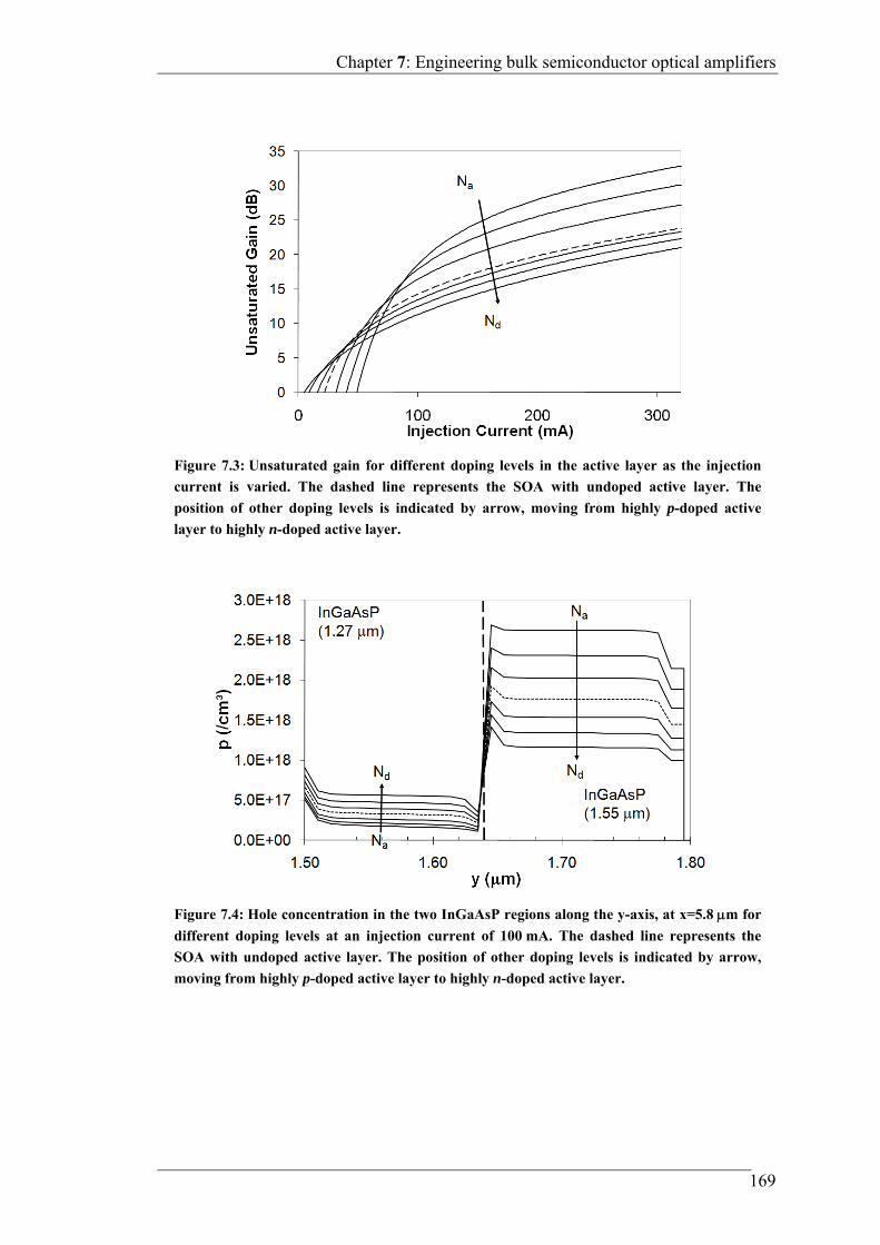
Chapter 7: Engineering bulk semiconductor optical amplifiers
169
Figure 7.3: Unsaturated gain for different doping levels in the active layer as the injection
current is varied. The dashed line represents the SOA with undoped active layer. The
position of other doping levels is indicated by arrow, moving from highly p-doped active
layer to highly n-doped active layer.
Figure 7.4: Hole concentration in the two InGaAsP regions along the y-axis, at x=5.8 m for
different doping levels at an injection current of 100 mA. The dashed line represents the
SOA with undoped active layer. The position of other doping levels is indicated by arrow,
moving from highly p-doped active layer to highly n-doped active layer.
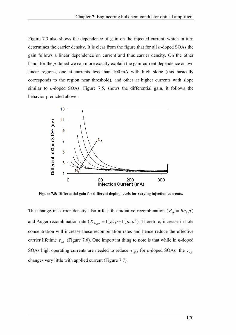
Chapter 7: Engineering bulk semiconductor optical amplifiers
170
Figure 7.3 also shows the dependence of gain on the injected current, which in turn
determines the carrier density. It is clear from the figure that for all n-doped SOAs the
gain follows a linear dependence on current and thus carrier density. On the other
hand, for the p-doped we can more exactly explain the gain-current dependence as two
linear regions, one at currents less than 100 mA with high slope (this basically
corresponds to the region near threshold), and other at higher currents with slope
similar to n-doped SOAs. Figure 7.5, shows the differential gain, it follows the
behavior predicted above.
The change in carrier density also affect the radiative recombination ( pBnR Tsp )
and Auger recombination rate ( 22 pnpnR TpTnAuger ). Therefore, increase in hole
concentration will increase these recombination rates and hence reduce the effective
carrier lifetime eff (Figure 7.6). One important thing to note is that while in n-doped
SOAs high operating currents are needed to reduce eff , for p-doped SOAs the eff
changes very little with applied current (Figure 7.7).
Figure 7.5: Differential gain for different deping levels for varying injection currents.
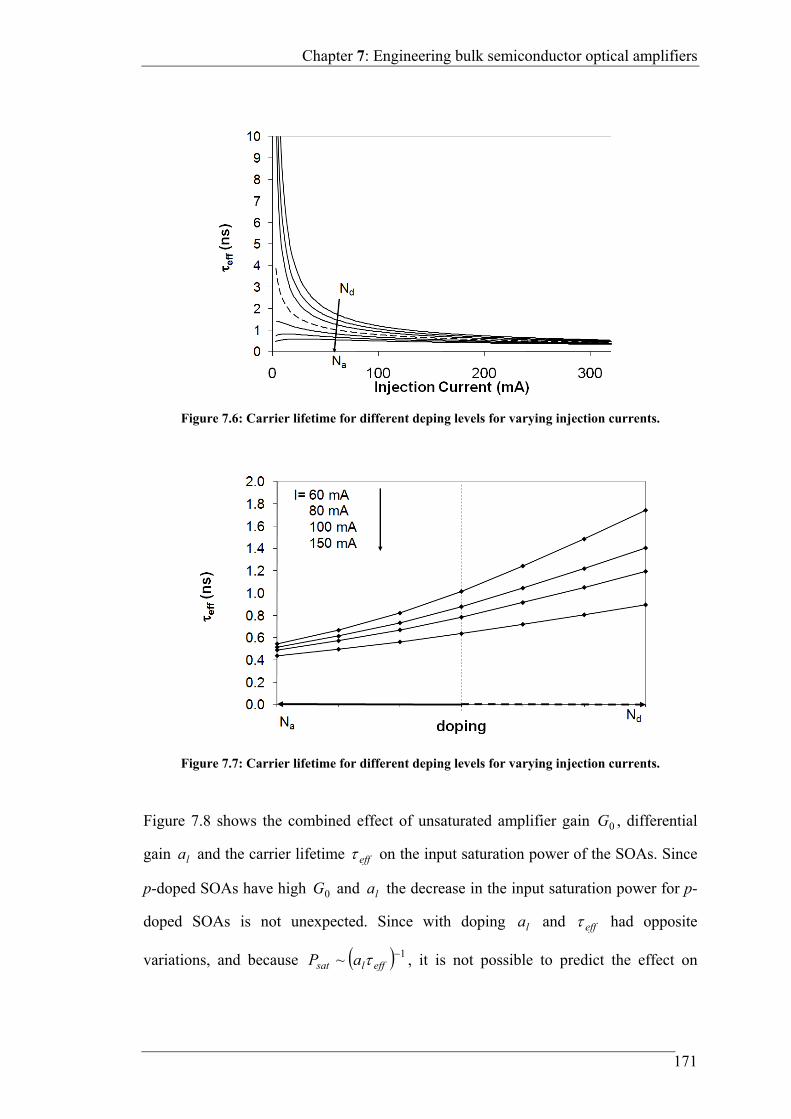
Chapter 7: Engineering bulk semiconductor optical amplifiers
171
Figure 7.8 shows the combined effect of unsaturated amplifier gain 0G , differential
gain la and the carrier lifetime eff on the input saturation power of the SOAs. Since
p-doped SOAs have high 0G and la the decrease in the input saturation power for p-
doped SOAs is not unexpected. Since with doping la and eff had opposite
variations, and because 1~ efflsat aP , it is not possible to predict the effect on
Figure 7.6: Carrier lifetime for different deping levels for varying injection currents.
Figure 7.7: Carrier lifetime for different deping levels for varying injection currents.
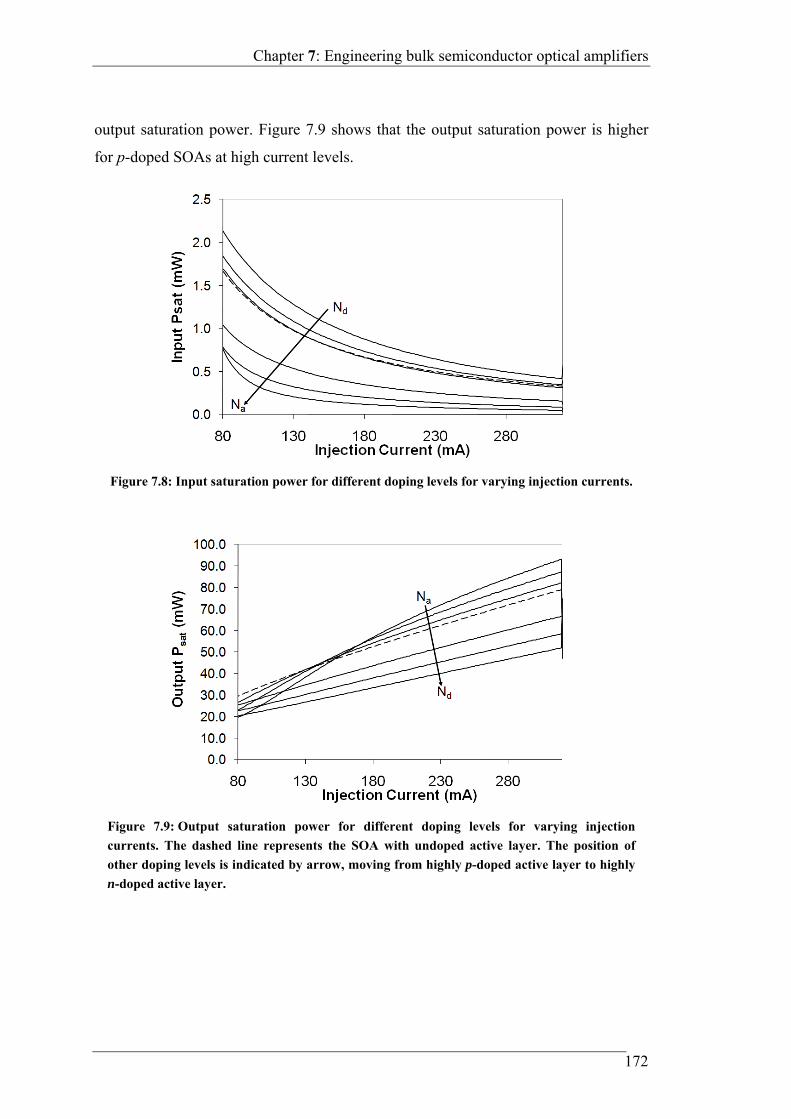
Chapter 7: Engineering bulk semiconductor optical amplifiers
172
output saturation power. Figure 7.9 shows that the output saturation power is higher
for p-doped SOAs at high current levels.
Figure 7.8: Input saturation power for different doping levels for varying injection currents.
Figure 7.9: Output saturation power for different doping levels for varying injection
currents. The dashed line represents the SOA with undoped active layer. The position of
other doping levels is indicated by arrow, moving from highly p-doped active layer to highly
n-doped active layer.
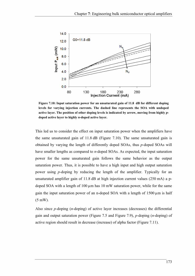
Chapter 7: Engineering bulk semiconductor optical amplifiers
173
This led us to consider the effect on input saturation power when the amplifiers have
the same unsaturated gain of 11.8 dB (Figure 7.10). The same unsaturated gain is
obtained by varying the length of differently doped SOAs, thus p-doped SOAs will
have smaller lengths as compared to n-doped SOAs. As expected, the input saturation
power for the same unsaturated gain follows the same behavior as the output
saturation power. Thus, it is possible to have a high input and high output saturation
power using p-doping by reducing the length of the amplifier. Typically for an
unsaturated amplifier gain of 11.8 dB at high injection current values (250 mA) a p-
doped SOA with a length of 100 m has 10 mW saturation power, while for the same
gain the input saturation power of an n-doped SOA with a length of 1500 m is half
(5 mW).
Also since p-doping (n-doping) of active layer increases (decreases) the differential
gain and output saturation power (Figure 7.5 and Figure 7.9), p-doping (n-doping) of
active region should result in decrease (increase) of alpha factor (Figure 7.11).
Figure 7.10: Input saturation power for an unsaturated gain of 11.8 dB for different doping
levels for varying injection currents. The dashed line represents the SOA with undoped
active layer. The position of other doping levels is indicated by arrow, moving from highly p-
doped active layer to highly n-doped active layer.
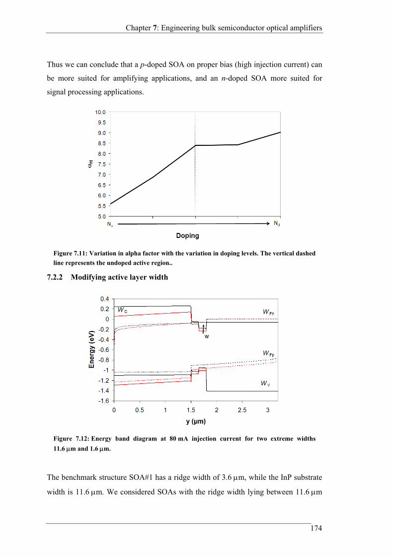
Chapter 7: Engineering bulk semiconductor optical amplifiers
174
Thus we can conclude that a p-doped SOA on proper bias (high injection current) can
be more suited for amplifying applications, and an n-doped SOA more suited for
signal processing applications.
7.2.2 Modifying active layer width
The benchmark structure SOA#1 has a ridge width of 3.6 m, while the InP substrate
width is 11.6 m. We considered SOAs with the ridge width lying between 11.6 m
Figure 7.11: Variation in alpha factor with the variation in doping levels. The vertical dashed
line represents the undoped active region..
Figure 7.12: Energy band diagram at 80 mA injection current for two extreme widths
11.6 m and 1.6 m.
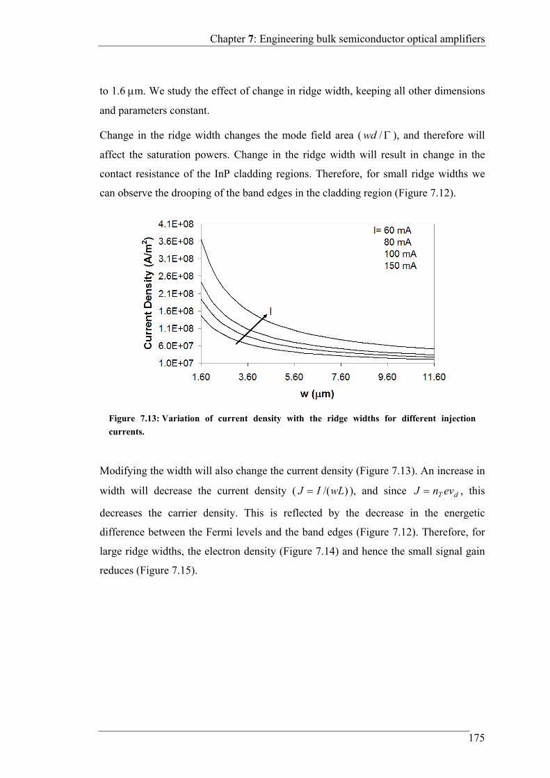
Chapter 7: Engineering bulk semiconductor optical amplifiers
175
to 1.6 m. We study the effect of change in ridge width, keeping all other dimensions
and parameters constant.
Change in the ridge width changes the mode field area ( /wd ), and therefore will
affect the saturation powers. Change in the ridge width will result in change in the
contact resistance of the InP cladding regions. Therefore, for small ridge widths we
can observe the drooping of the band edges in the cladding region (Figure 7.12).
Modifying the width will also change the current density (Figure 7.13). An increase in
width will decrease the current density ( )/(wLIJ ), and since dT evnJ , this
decreases the carrier density. This is reflected by the decrease in the energetic
difference between the Fermi levels and the band edges (Figure 7.12). Therefore, for
large ridge widths, the electron density (Figure 7.14) and hence the small signal gain
reduces (Figure 7.15).
Figure 7.13: Variation of current density with the ridge widths for different injection
currents.
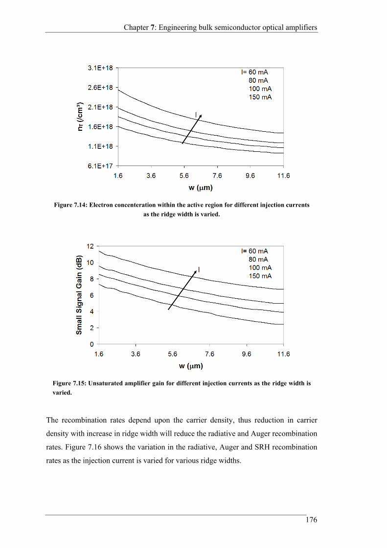
Chapter 7: Engineering bulk semiconductor optical amplifiers
176
The recombination rates depend upon the carrier density, thus reduction in carrier
density with increase in ridge width will reduce the radiative and Auger recombination
rates. Figure 7.16 shows the variation in the radiative, Auger and SRH recombination
rates as the injection current is varied for various ridge widths.
Figure 7.14: Electron concenteration within the active region for different injection currents
as the ridge width is varied.
Figure 7.15: Unsaturated amplifier gain for different injection currents as the ridge width is
varied.
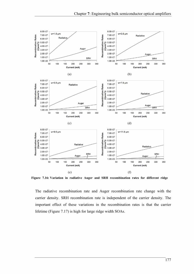
Chapter 7: Engineering bulk semiconductor optical amplifiers
177
The radiative recombination rate and Auger recombination rate change with the
carrier density. SRH recombination rate is independent of the carrier density. The
important effect of these variations in the recombination rates is that the carrier
lifetime (Figure 7.17) is high for large ridge width SOAs.
(a) (b)
(c) (d)
(e) (f)
Figure 7.16: Variation in radiative Auger and SRH recombination rates for different ridge
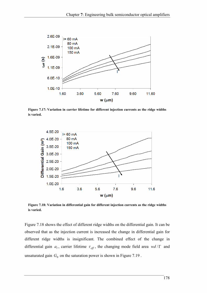
Chapter 7: Engineering bulk semiconductor optical amplifiers
178
Figure 7.18 shows the effect of different ridge widths on the differential gain. It can be
observed that as the injection current is increased the change in differential gain for
different ridge widths is insignificant. The combined effect of the change in
differential gain la , carrier lifetime eff , the changing mode field area /wd and
unsaturated gain 0G on the saturation power is shown in Figure 7.19 .
Figure 7.17: Variation in carrier lifetime for different injection currents as the ridge widths
is varied.
Figure 7.18: Variation in differential gain for different injection currents as the ridge widths
is varied.
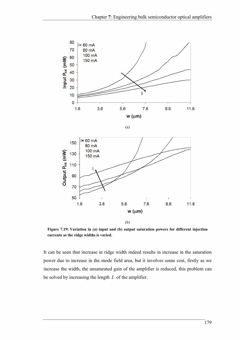
Chapter 7: Engineering bulk semiconductor optical amplifiers
179
It can be seen that increase in ridge width indeed results in increase in the saturation
power due to increase in the mode field area, but it involves some cost, firstly as we
increase the width, the unsaturated gain of the amplifier is reduced, this problem can
be solved by increasing the length L of the amplifier.
(a)
(b)
Figure 7.19: Variation in (a) input and (b) output saturation powers for different injection
currents as the ridge widths is varied.
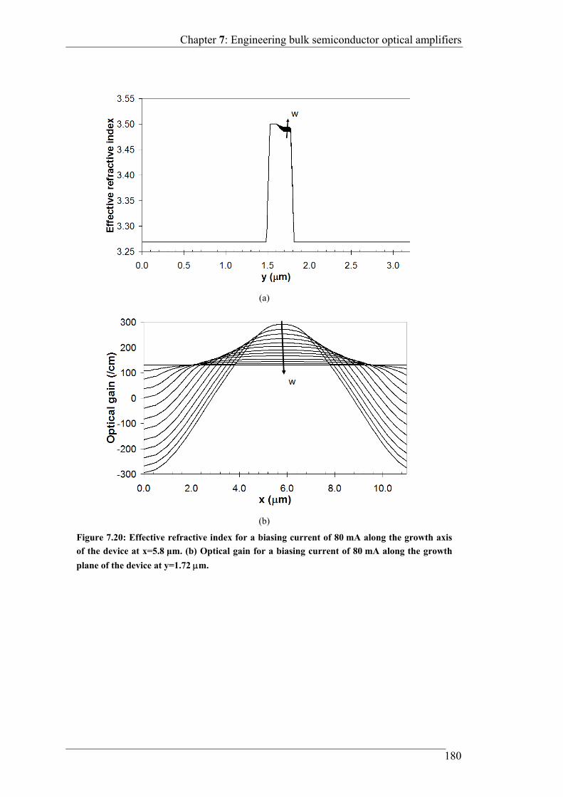
Chapter 7: Engineering bulk semiconductor optical amplifiers
180
(a)
(b)
Figure 7.20: Effective refractive index for a biasing current of 80 mA along the growth axis
of the device at x=5.8 μm. (b) Optical gain for a biasing current of 80 mA along the growth
plane of the device at y=1.72 m.
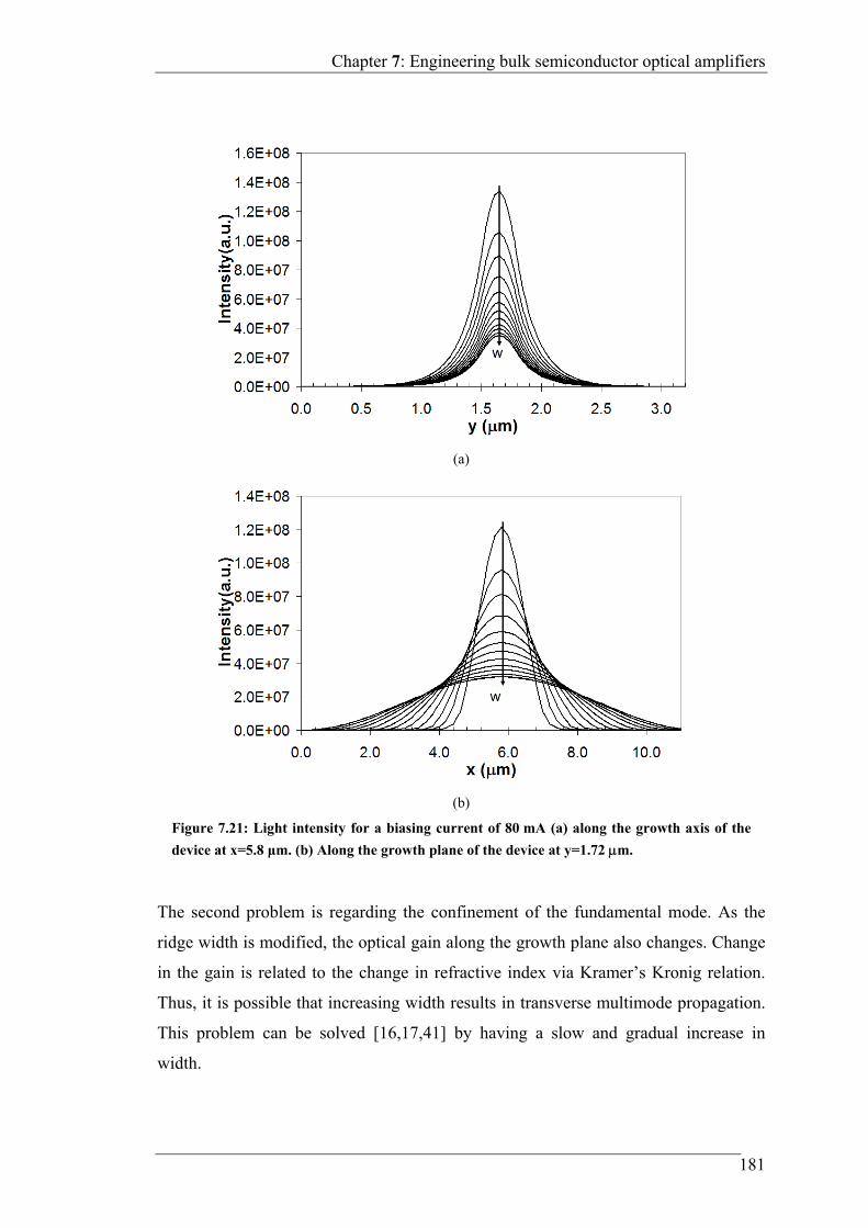
Chapter 7: Engineering bulk semiconductor optical amplifiers
181
The second problem is regarding the confinement of the fundamental mode. As the
ridge width is modified, the optical gain along the growth plane also changes. Change
in the gain is related to the change in refractive index via Kramer’s Kronig relation.
Thus, it is possible that increasing width results in transverse multimode propagation.
This problem can be solved [16,17,41] by having a slow and gradual increase in
width.
(a)
(b)
Figure 7.21: Light intensity for a biasing current of 80 mA (a) along the growth axis of the
device at x=5.8 μm. (b) Along the growth plane of the device at y=1.72 m.
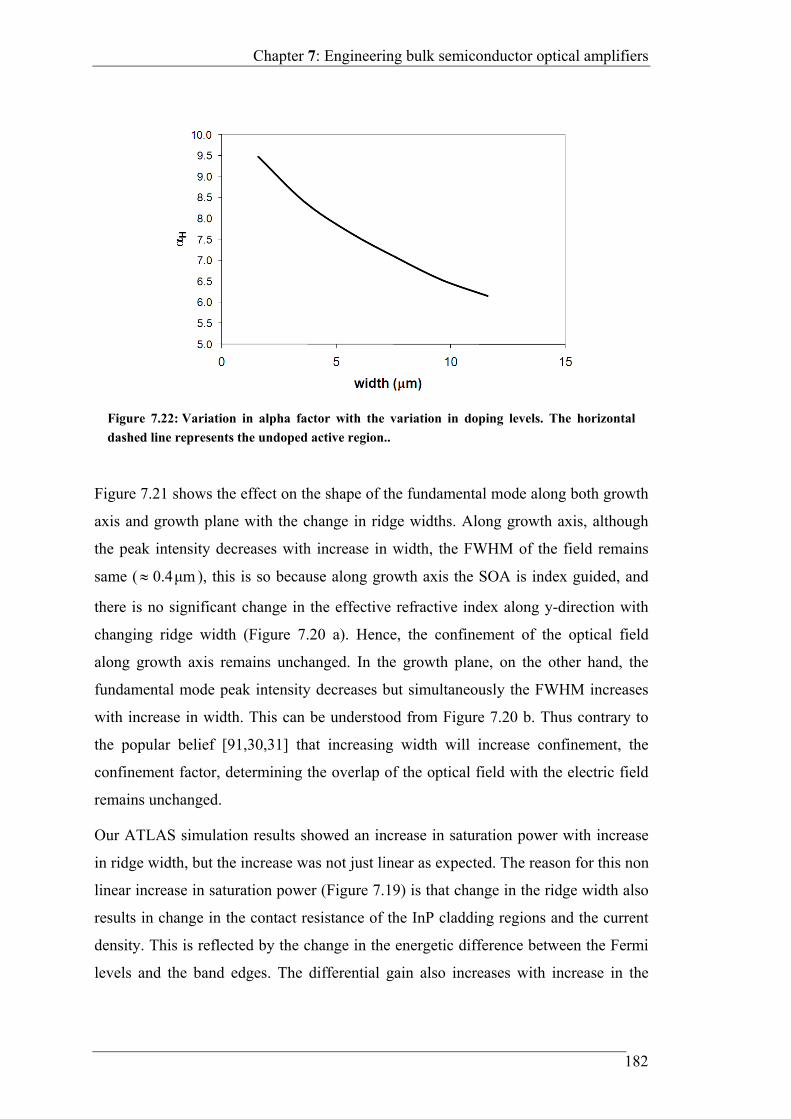
Chapter 7: Engineering bulk semiconductor optical amplifiers
182
Figure 7.21 shows the effect on the shape of the fundamental mode along both growth
axis and growth plane with the change in ridge widths. Along growth axis, although
the peak intensity decreases with increase in width, the FWHM of the field remains
same ( μm4.0 ), this is so because along growth axis the SOA is index guided, and
there is no significant change in the effective refractive index along y-direction with
changing ridge width (Figure 7.20 a). Hence, the confinement of the optical field
along growth axis remains unchanged. In the growth plane, on the other hand, the
fundamental mode peak intensity decreases but simultaneously the FWHM increases
with increase in width. This can be understood from Figure 7.20 b. Thus contrary to
the popular belief [91,30,31] that increasing width will increase confinement, the
confinement factor, determining the overlap of the optical field with the electric field
remains unchanged.
Our ATLAS simulation results showed an increase in saturation power with increase
in ridge width, but the increase was not just linear as expected. The reason for this non
linear increase in saturation power (Figure 7.19) is that change in the ridge width also
results in change in the contact resistance of the InP cladding regions and the current
density. This is reflected by the change in the energetic difference between the Fermi
levels and the band edges. The differential gain also increases with increase in the
Figure 7.22: Variation in alpha factor with the variation in doping levels. The horizontal
dashed line represents the undoped active region..

Chapter 7: Engineering bulk semiconductor optical amplifiers
183
ridge width. This suggests that alpha factor should decrease with increase the ridge
width, as is observed (Figure 7.22).
Thus we can conclude that since SOAs with small active layer depth have reduced
effective carrier lifetime, low saturation powers, and high alpha factor they are better
suited as optical signal processing applications. In case we want to design an SOA for
in-line amplification application, the best design will be a gradually increasing tapered
structure. Small width in the beginning of SOA will enable a fast response, and
growing width along the length of SOA will increase the saturation power.
7.2.3 Modifying active layer depth
The benchmark structure SOA#1 has an active layer depth of 0.15 m. We considered
SOAs with the active layer depth lying between 3.0 m to 0.8 m11. We study the
effect of change active layer depth, keeping all other dimensions and parameters
constant.
11 Below 0.8 m the SOA active layer is no longer a bulk structure and should be treated as quantum
well.
Figure 7.23: Confinement factor for different injection currents as the depth of the active
region is varied.
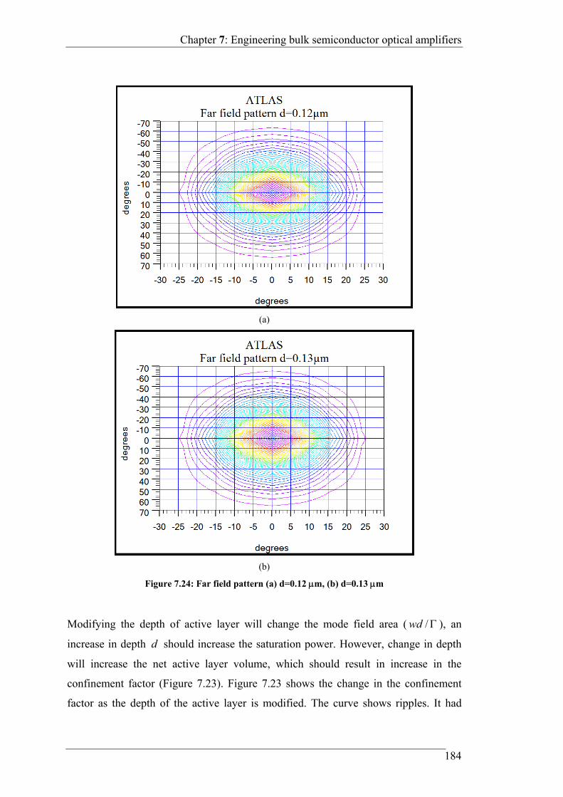
Chapter 7: Engineering bulk semiconductor optical amplifiers
184
Modifying the depth of active layer will change the mode field area ( /wd ), an
increase in depth d should increase the saturation power. However, change in depth
will increase the net active layer volume, which should result in increase in the
confinement factor (Figure 7.23). Figure 7.23 shows the change in the confinement
factor as the depth of the active layer is modified. The curve shows ripples. It had
(a)
(b)
Figure 7.24: Far field pattern (a) d=0.12 m, (b) d=0.13 m
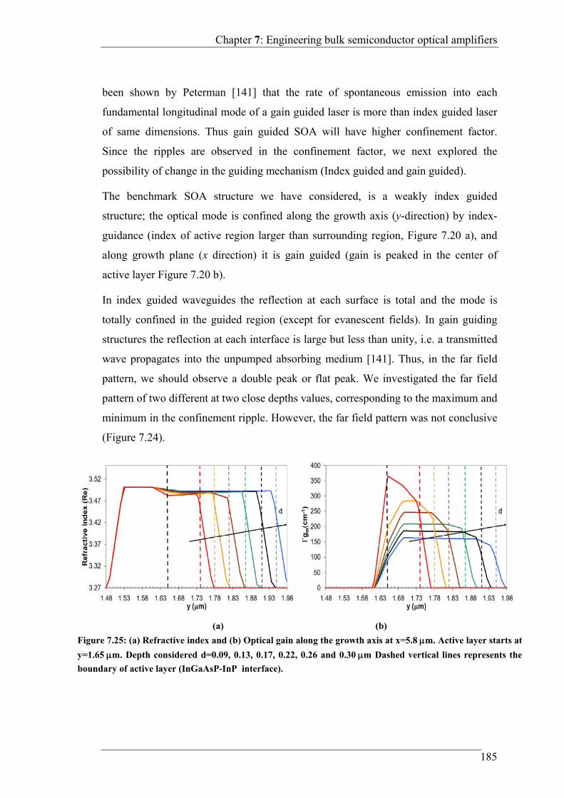
Chapter 7: Engineering bulk semiconductor optical amplifiers
185
been shown by Peterman [141] that the rate of spontaneous emission into each
fundamental longitudinal mode of a gain guided laser is more than index guided laser
of same dimensions. Thus gain guided SOA will have higher confinement factor.
Since the ripples are observed in the confinement factor, we next explored the
possibility of change in the guiding mechanism (Index guided and gain guided).
The benchmark SOA structure we have considered, is a weakly index guided
structure; the optical mode is confined along the growth axis (y-direction) by index-
guidance (index of active region larger than surrounding region, Figure 7.20 a), and
along growth plane (x direction) it is gain guided (gain is peaked in the center of
active layer Figure 7.20 b).
In index guided waveguides the reflection at each surface is total and the mode is
totally confined in the guided region (except for evanescent fields). In gain guiding
structures the reflection at each interface is large but less than unity, i.e. a transmitted
wave propagates into the unpumped absorbing medium [141]. Thus, in the far field
pattern, we should observe a double peak or flat peak. We investigated the far field
pattern of two different at two close depths values, corresponding to the maximum and
minimum in the confinement ripple. However, the far field pattern was not conclusive
(Figure 7.24).
(a) (b)
Figure 7.25: (a) Refractive index and (b) Optical gain along the growth axis at x=5.8 m. Active layer starts at
y=1.65 m. Depth considered d=0.09, 0.13, 0.17, 0.22, 0.26 and 0.30 m Dashed vertical lines represents the
boundary of active layer (InGaAsP-InP interface).
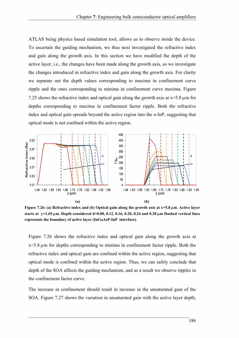
Chapter 7: Engineering bulk semiconductor optical amplifiers
186
ATLAS being physics based simulation tool, allows us to observe inside the device.
To ascertain the guiding mechanism, we thus next investigated the refractive index
and gain along the growth axis. In this section we have modified the depth of the
active layer, i.e., the changes have been made along the growth axis, so we investigate
the changes introduced in refractive index and gain along the growth axis. For clarity
we separate out the depth values corresponding to maxima in confinement curve
ripple and the ones corresponding to minima in confinement curve maxima. Figure
7.25 shows the refractive index and optical gain along the growth axis at x=5.8 m for
depths corresponding to maxima in confinement factor ripple. Both the refractive
index and optical gain spreads beyond the active region into the n-InP, suggesting that
optical mode is not confined within the active region.
Figure 7.26 shows the refractive index and optical gain along the growth axis at
x=5.8 m for depths corresponding to minima in confinement factor ripple. Both the
refractive index and optical gain are confined within the active region, suggesting that
optical mode is confined within the active region. Thus, we can safely conclude that
depth of the SOA affects the guiding mechanism, and as a result we observe ripples in
the confinement factor curve.
The increase in confinement should result in increase in the unsaturated gain of the
SOA. Figure 7.27 shows the variation in unsaturated gain with the active layer depth,
(a) (b)
Figure 7.26: (a) Refractive index and (b) Optical gain along the growth axis at x=5.8 m. Active layer
starts at y=1.65 m. Depth considered d=0.08, 0.12, 0.16, 0.20, 0.24 and 0.28 m Dashed vertical lines
represents the boundary of active layer (InGaAsP-InP interface).
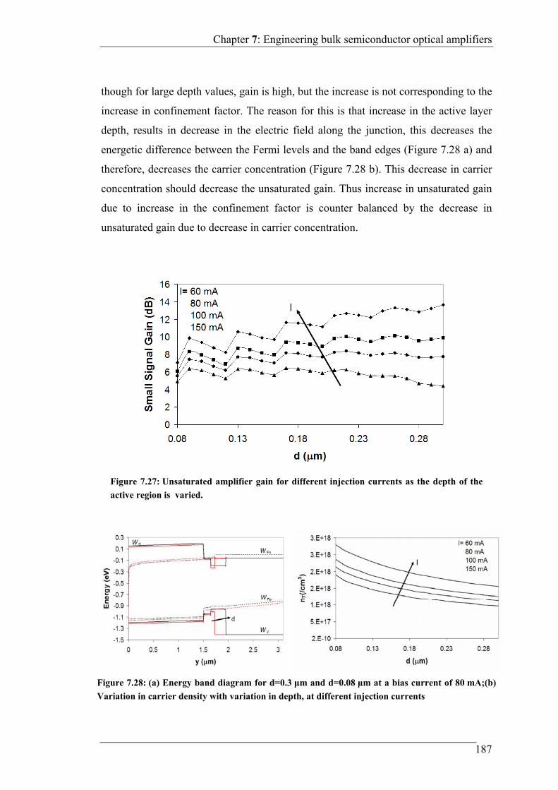
Chapter 7: Engineering bulk semiconductor optical amplifiers
187
though for large depth values, gain is high, but the increase is not corresponding to the
increase in confinement factor. The reason for this is that increase in the active layer
depth, results in decrease in the electric field along the junction, this decreases the
energetic difference between the Fermi levels and the band edges (Figure 7.28 a) and
therefore, decreases the carrier concentration (Figure 7.28 b). This decrease in carrier
concentration should decrease the unsaturated gain. Thus increase in unsaturated gain
due to increase in the confinement factor is counter balanced by the decrease in
unsaturated gain due to decrease in carrier concentration.
Figure 7.27: Unsaturated amplifier gain for different injection currents as the depth of the
active region is varied.
Figure 7.28: (a) Energy band diagram for d=0.3 μm and d=0.08 μm at a bias current of 80 mA;(b)
Variation in carrier density with variation in depth, at different injection currents

Chapter 7: Engineering bulk semiconductor optical amplifiers
188
The decrease in carrier concentration will decrease the recombination rates and thus
increase the effective carrier lifetime (Figure 7.29 a). Figure 7.29 b shows the
variation in differential gain with the variation in depth. Since both effective carrier
lifetime and differential gain increase for SOAs with large depth values, the saturation
power decreases for SOAs with large active layer depth. The ripples in the
confinement curve carry themselves (in reverse direction) in the saturation power
curves.
Figure 7.30 shows the input saturation power for SOAs with different active layer
depth. Since the gain is not much affected by different active layer depths, the output
saturation power also decreases with increase in active layer depth.
Thus we can conclude that as we decrease the depth of active region, the decreased
confinement factor, and reduced effective carrier lifetime, increases both input and
output saturation power, making an SOA with small active layer depths a better choice
for in-line optical amplification.
Figure 7.29: (a) Effective carrier lifetime for different injection currents as the depth of the active
region is varied; (b) Differential gain for different injection currents as the depth of the active
region

Chapter 7: Engineering bulk semiconductor optical amplifiers
189
7.3 Summary
In this chapter we showed that bulk SOA can be engineered for both low and high
saturation power and alpha factor. Specifically, we considered how the modifications
in doping, active layer depth and ridge width affect saturation powers, effective carrier
lifetime and alpha factor; giving us guideline on what parameters to be modified for
specific SOA applications.
Figure 7.30: Input saturation power for different injection currents as the depth of the active
region is varied.
Figure 7.31: Output saturation power for different injection currents as the depth of the
active region is varied.
Chapter 7: Engineering bulk semiconductor optical amplifiers
190
Our results show that a p-doped SOA on proper bias (high injection current) can be
more suited for amplifying applications, and an n-doped SOA more suited for signal
processing applications.
Small active layer depth reduces effective carrier lifetime, saturation powers, and at
same time increase alpha factor thus they are better suited as optical signal processing
applications. In case we want to design an SOA for in-line amplification application,
the best design will be a gradually increasing tapered structure. Small width in the
beginning of SOA will enable a fast response, and growing width along the length of
SOA will increase the saturation power.
We were able to both increase and decrease the alpha factor from the benchmark SOA
value by changing both the doping of the active region and the ridge width. We
obtained about 34% decrease in the value of alpha factor by introducing acceptor
doping in the active region to the present practical limit for InGaAsP ( 318 cm102 )
and also by increasing the ridge width to the maximum possible value (11.6 m) for
the existing structure.
Our results show that decrease in the depth of active region, the decreases
confinement factor, and reduces effective carrier lifetime this increases both input and
output saturation power, making an SOA with small active layer depths a better choice
for in-line optical amplification.
This work in parts has been reported in the following Publications:
Amita Kapoor, E. K Sharma, W. Freude and J. Leuthold, Saturation
Characteristics of InGaAsP-InP bulk SOA, Proc. of SPIE 7597, 75971I,
(2010).
W. Freude, R. Bonk, T. Vallaitis, A. Marculescu, Amita Kapoor, C. Meuer,
D. Bimberg, R. Brenot, F. Lelarge, G. H. Duan, and J. Leuthold,
Semiconductor optical amplifiers (SOA) for linear and nonlinear applications,
Deutsche Physikalische Gesellschaft e.V., Regensberg , 21-26 March (2010).
W. Freude, R. Bonk, T. Vallaitis, A. Marculescu, Amita Kapoor,
E. K. Sharma, ,C. Meuer, D. Bimberg, R. Brenot, F. Lelarge, G. H. Duan, and

Chapter 7: Engineering bulk semiconductor optical amplifiers
191
J. Leuthold, Linear and nonlinear semiconductor optical amplifiers, ICTON,
27 June- 1 July (2010).

Chapter 8: Long period gratings: Refractive index sensor
193
8 Long period gratings: Refractive index sensor
8.1 Introduction
Measurement of Refractive Index (RI) is an important task today not only in
engineering applications but also in biomedical sciences. The refractive index of a
liquid, under isothermal conditions, is a function of concentration only. Thus, precise
and accurate measurement of refractive index has been employed to determine the
purity of liquids such as water, kerosene etc [7,106]. RI is also a biophysical property
of the living cell, in particular it is related to the intracellular protein concentration
[132]. Various pathological states alter the RI of cell. Hence, measurement of RI has
been used to determine various pathological conditions involving E. Coli [75],
Erythrocytes [105], and quality assurance of pediatric parentral nutrient solutions [88].
The standard method of measuring RI is the use of Abbe Refractometer, which
generally involves sending the sample to a laboratory, a costly, time consuming
process that is not susceptible to real time monitoring. Therefore, it is natural to
consider the utilization of optical fiber technology to measure the refractive index
because of its unique characteristics such as: ease of fabrication, low insertion loss,
high sensitivity, fast response and compactness. More specifically Long Period
Chapter 8: Long period gratings: Refractive index sensor
194
Gratings (LPG) have been used as sensors for various physical properties such as
strain, temperature and refractive index.
As discussed in Chapter 2, a LPG couples the power from the forward propagating
core mode to the co-propagating cladding modes. The cladding modes can be easily
attenuated by a small bend and this results in the transmission spectrum of the fiber
containing a series of attenuation bands centered at discrete wavelengths, with each
attenuation band corresponding to the coupling to a different cladding mode
[19,44,45,117,134]. A specific feature of LPGs is the sensitivity of the transmission
spectrum to the refractive index of ambient ambn , i.e., the material surrounding the
cladding of fiber [19,134], because the effective indices of the cladding modes, mcleffn , ,
are strongly influenced by the ambient refractive index. The primary effect of change
in the ambient refractive index is the consequent change in resonant wavelength.
Hence, several authors have exploited this feature of a LPG to implement refractive
index sensors based on the change in resonance wavelength, [18,96,115,134,146], i.e.,
they measure the small shift in the resonance wavelength with change in ambient
refractive index. The limitation of this technique is that the measurement of such small
wavelength shifts requires the use of relatively expensive high-resolution optical
spectrum analyzers (OSA).
We present an alternative approach for measurement of refractive index using a LPG.
In our method a LPG is interrogated by a single wavelength source and, instead of
measuring the shift in resonance, the change in the power retained in the core mode
due to change in ambient index is measured. We present a criterion to design the
grating, which takes into account the desired refractive index range and maximizes the
sensitivity in a LPG fabricated in a standard fiber when the interrogating wavelength
is fixed. To illustrate the use of design criterion we present the design of a LPG in a
standard SMF28 [32] fiber for specific application to refractive index variation of
sugar solution with concentration and detection of mole fraction of xylene in heptane
(paraffin) [7]. It should be mentioned that Bhatia and Vengsarkar [19] did propose a
demodulation scheme that made use of a laser source centered away from resonance
wavelength for converting the wavelength to intensity variation in a temperature
Chapter 8: Long period gratings: Refractive index sensor
195
sensor. However, no specific design criteria for the choice of wavelength, cladding
mode and grating period have been reported.
8.2 Conventional refractometers
The standard way to measure refractive index of solids and liquid (mainly transparent
or semitransparent) is by the use of Abbe refractometer, developed by Ernst Abbe in
the late 1800s. The basic principle of the refractometer is the application of the Snell’s
Law, i.e. when light passes through the interface of two different media then, the ratio
of the sines of the angles of incidence and refraction is equivalent to the ratio of
velocities in the two media or equivalent to the opposite ratio of the refractive indices.
1
2
2
1
2
1
sin
sin
n
n
v
v
(8.1)
where 1 is the angle of incidence, 2 is the angle of refraction, 2,1iv is the velocity
of light in the medium, and 2,1in is the refractive index of medium (i is 1 for first
medium, and 2 for second medium). If the second medium has low refractive index it
is possible to obtain an incidence angle is for which the refracting angle is 90 i.e., the
light does not enter the second medium. This incident angle is called the critical angle
c .
In Abbe’s refractometer the sample is sandwiched into a thin layer between an
illuminating prism and a refracting prism. The refracting prism is made of a material
with high refractive index, and the refractometer is designed to measure samples
having smaller refractive index than that of refracting prism. Using Abbe
refractometer the critical angle for the liquid is determined, which is then used to
calculate the refractive index of the liquid.
Density of liquid usually decreases with increase in temperature; this results in
increase in speed of light and hence changes the refractive index of the liquid. To
maintain a constant temperature, refractometer is equipped with a thermometer and a
means of circulating water through the refractometer.
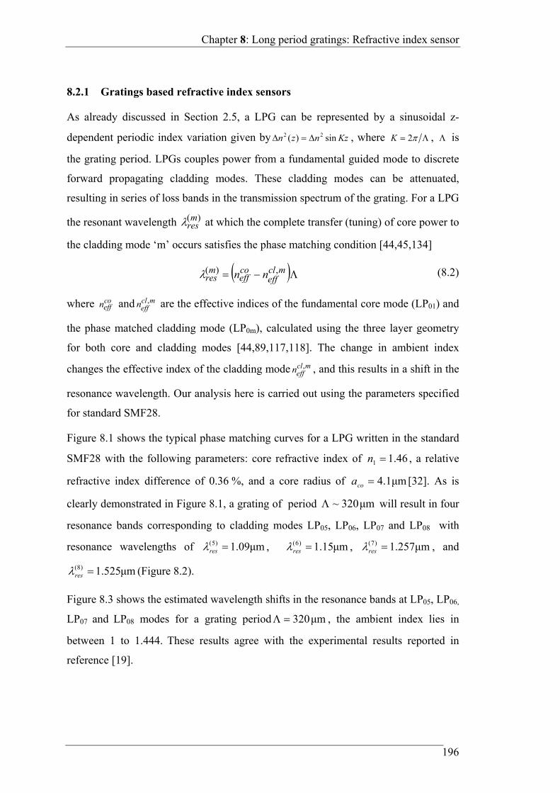
Chapter 8: Long period gratings: Refractive index sensor
196
8.2.1 Gratings based refractive index sensors
As already discussed in Section 2.5, a LPG can be represented by a sinusoidal z-
dependent periodic index variation given by Kznzn sin)( 22 , where 2K , is
the grating period. LPGs couples power from a fundamental guided mode to discrete
forward propagating cladding modes. These cladding modes can be attenuated,
resulting in series of loss bands in the transmission spectrum of the grating. For a LPG
the resonant wavelength )(mres at which the complete transfer (tuning) of core power to
the cladding mode ‘m’ occurs satisfies the phase matching condition [44,45,134]
mcleff
coeff
mres nn ,)( (8.2)
where coeffn and mcl
effn , are the effective indices of the fundamental core mode (LP01) and
the phase matched cladding mode (LP0m), calculated using the three layer geometry
for both core and cladding modes [44,89,117,118]. The change in ambient index
changes the effective index of the cladding mode mcleffn , , and this results in a shift in the
resonance wavelength. Our analysis here is carried out using the parameters specified
for standard SMF28.
Figure 8.1 shows the typical phase matching curves for a LPG written in the standard
SMF28 with the following parameters: core refractive index of 46.11 n , a relative
refractive index difference of 0.36 %, and a core radius of μm1.4coa [32]. As is
clearly demonstrated in Figure 8.1, a grating of period μm320~ will result in four
resonance bands corresponding to cladding modes LP05, LP06, LP07 and LP08 with
resonance wavelengths of μm09.1)5( res , μm15.1)6( res , μm257.1)7( res , and
μm525.1)8( res (Figure 8.2).
Figure 8.3 shows the estimated wavelength shifts in the resonance bands at LP05, LP06,
LP07 and LP08 modes for a grating period μm320 , the ambient index lies in
between 1 to 1.444. These results agree with the experimental results reported in
reference [19].
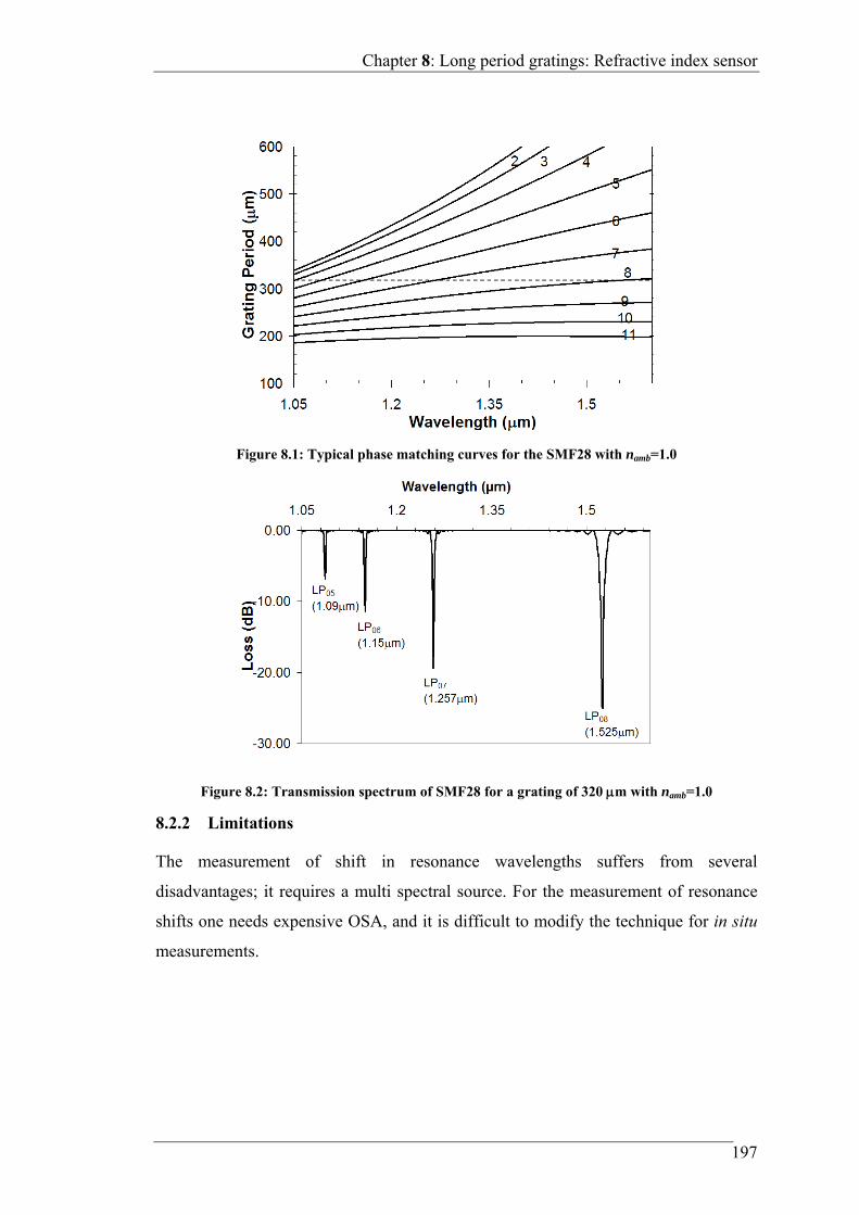
Chapter 8: Long period gratings: Refractive index sensor
197
8.2.2 Limitations
The measurement of shift in resonance wavelengths suffers from several
disadvantages; it requires a multi spectral source. For the measurement of resonance
shifts one needs expensive OSA, and it is difficult to modify the technique for in situ
measurements.
Figure 8.1: Typical phase matching curves for the SMF28 with namb=1.0
Figure 8.2: Transmission spectrum of SMF28 for a grating of 320 m with namb=1.0
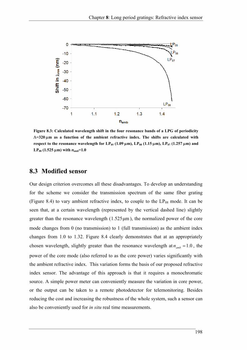
Chapter 8: Long period gratings: Refractive index sensor
198
8.3 Modified sensor
Our design criterion overcomes all these disadvantages. To develop an understanding
for the scheme we consider the transmission spectrum of the same fiber grating
(Figure 8.4) to vary ambient refractive index, to couple to the LP08 mode. It can be
seen that, at a certain wavelength (represented by the vertical dashed line) slightly
greater than the resonance wavelength ( μm525.1 ), the normalized power of the core
mode changes from 0 (no transmission) to 1 (full transmission) as the ambient index
changes from 1.0 to 1.32. Figure 8.4 clearly demonstrates that at an appropriately
chosen wavelength, slightly greater than the resonance wavelength at 0.1ambn , the
power of the core mode (also referred to as the core power) varies significantly with
the ambient refractive index. This variation forms the basis of our proposed refractive
index sensor. The advantage of this approach is that it requires a monochromatic
source. A simple power meter can conveniently measure the variation in core power,
or the output can be taken to a remote photodetector for telemonitoring. Besides
reducing the cost and increasing the robustness of the whole system, such a sensor can
also be conveniently used for in situ real time measurements.
Figure 8.3: Calculated wavelength shift in the four resonance bands of a LPG of periodicity
=320 m as a function of the ambient refractive index. The shifts are calculated with
respect to the resonance wavelength for LP05 (1.09 m), LP08 (1.15 m), LP07 (1.257 m) and
LP08 (1.525 m) with namb=1.0

Chapter 8: Long period gratings: Refractive index sensor
199
8.3.1 Mathematical analysis
The normalized power in the core guided mode after a propagation distance, z, in an
LPG is given by [48,134]:
)(sin1)0(
)( 22
2)(
zPzP
zP m
coco
co
(8.3)
where 2)(
2
4m
,
22 )(m
effn is the detuning factor,
)(,)( mcleff
coeff
meff nnn , and )(m is the coupling coefficient of LP0,m cladding mode. The
coupling coefficient is defined as
a
mcladcore
om rdrrnk
0
)(2)(
4 (8.4)
where core and )(mclad are the normalized core mode and cladding mode fields
respectively, normalized to 120
2
rdrneff and 20 k . We define a parameter
Figure 8.4: Transmission spectrum of the LPG with a periodicity of =320 m and couling
to the LP08 mode for different ambient refractive indices. The dashed line corresponds to
=1.525 m and shows that, as the ambient refractive index changes from namb=1.0 (lowest
curve) to namb=1.32 (highest curve), the normalized core power changes from no transmission
to full transmission.
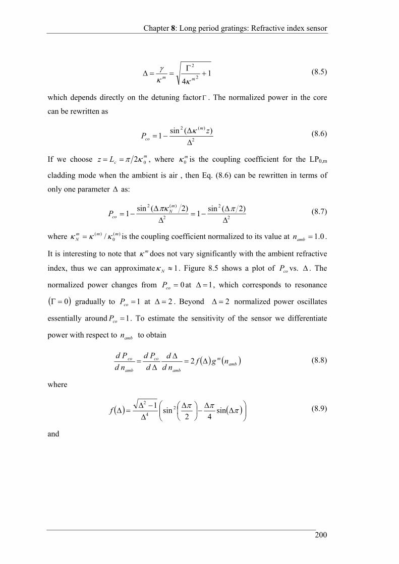
Chapter 8: Long period gratings: Refractive index sensor
200
14
2
2
mm
(8.5)
which depends directly on the detuning factor . The normalized power in the core
can be rewritten as
2
)(2 )(sin1
z
Pm
co
(8.6)
If we choose mcLz 02 , where m
0 is the coupling coefficient for the LP0,m
cladding mode when the ambient is air , then Eq. (8.6) can be rewritten in terms of
only one parameter as:
2
2
2
)(2 )2(sin1
)2(sin1
mN
coP (8.7)
where )(0
)( / mmmN is the coupling coefficient normalized to its value at 0.1ambn .
It is interesting to note that m does not vary significantly with the ambient refractive
index, thus we can approximate 1N . Figure 8.5 shows a plot of coP vs. . The
normalized power changes from 0coP at 1 , which corresponds to resonance
0 gradually to 1coP at 2 . Beyond 2 normalized power oscillates
essentially around 1coP . To estimate the sensitivity of the sensor we differentiate
power with respect to ambn to obtain
ambm
amb
co
amb
co ngfnd
d
d
Pd
nd
Pd
2 (8.8)
where
sin
42sin
1 2
4
2
f (8.9)
and
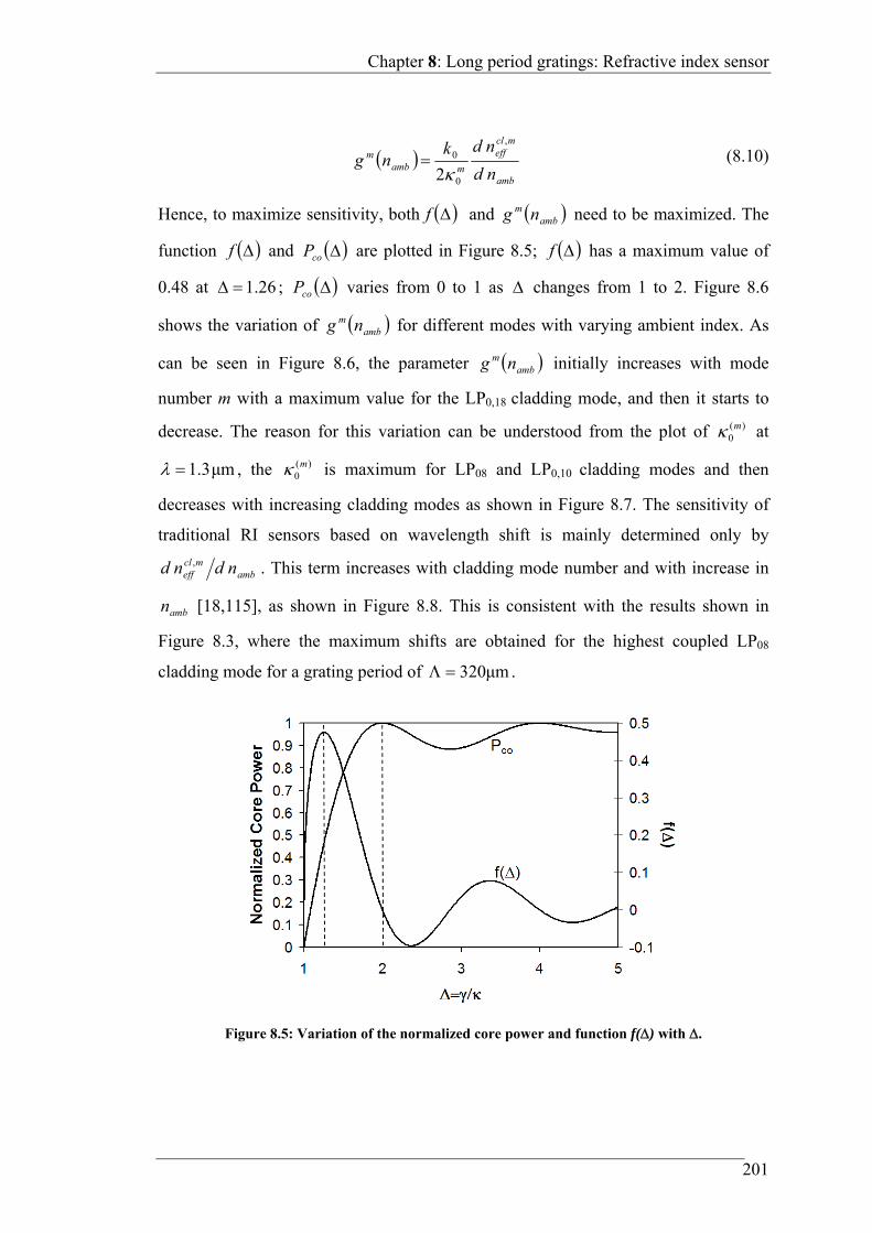
Chapter 8: Long period gratings: Refractive index sensor
201
amb
mcleff
mambm
nd
ndkng
,
0
0
2 (8.10)
Hence, to maximize sensitivity, both f and ambm ng need to be maximized. The
function f and coP are plotted in Figure 8.5; f has a maximum value of
0.48 at 26.1 ; coP varies from 0 to 1 as changes from 1 to 2. Figure 8.6
shows the variation of ambm ng for different modes with varying ambient index. As
can be seen in Figure 8.6, the parameter ambm ng initially increases with mode
number m with a maximum value for the LP0,18 cladding mode, and then it starts to
decrease. The reason for this variation can be understood from the plot of )(0
m at
μm3.1 , the )(0
m is maximum for LP08 and LP0,10 cladding modes and then
decreases with increasing cladding modes as shown in Figure 8.7. The sensitivity of
traditional RI sensors based on wavelength shift is mainly determined only by
ambmcl
eff ndnd , . This term increases with cladding mode number and with increase in
ambn [18,115], as shown in Figure 8.8. This is consistent with the results shown in
Figure 8.3, where the maximum shifts are obtained for the highest coupled LP08
cladding mode for a grating period of μm320 .
Figure 8.5: Variation of the normalized core power and function f() with .
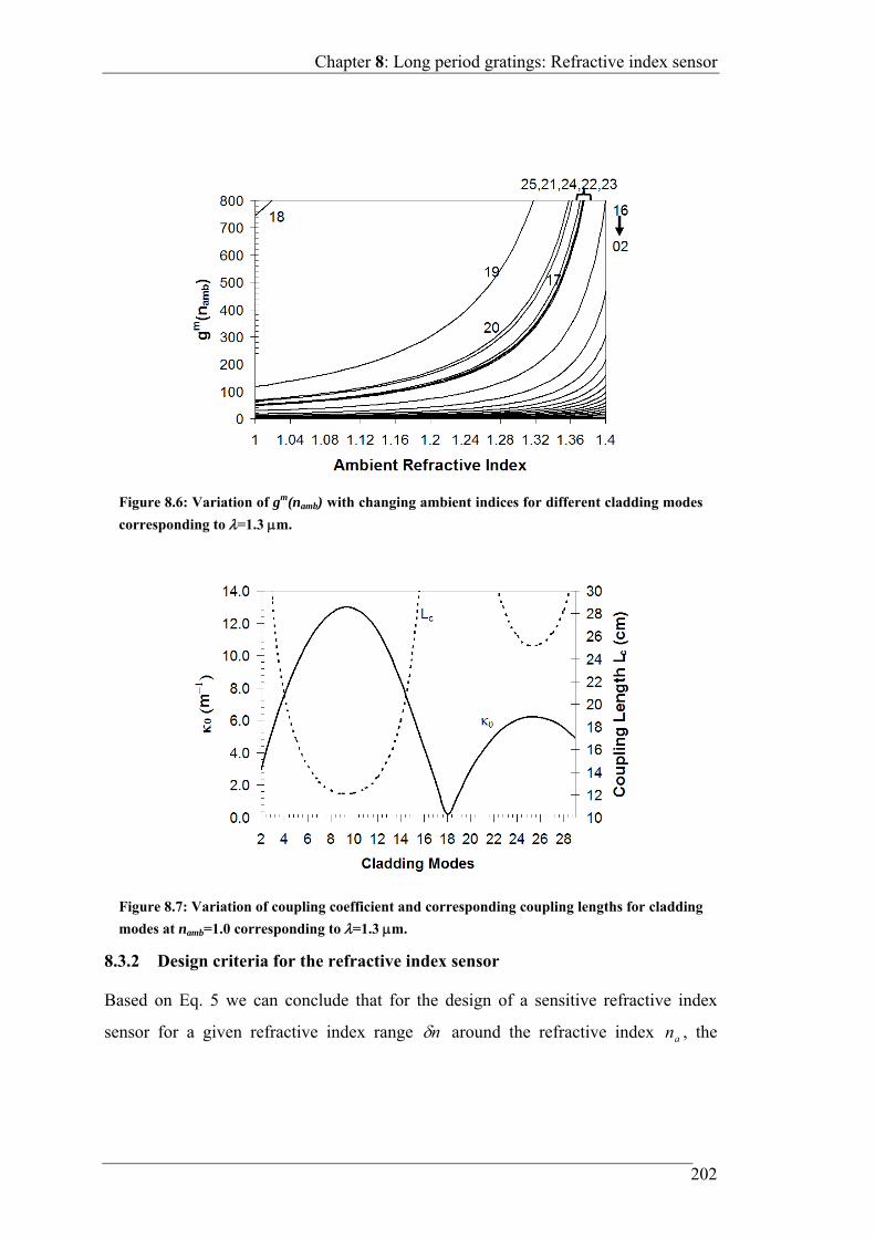
Chapter 8: Long period gratings: Refractive index sensor
202
8.3.2 Design criteria for the refractive index sensor
Based on Eq. 5 we can conclude that for the design of a sensitive refractive index
sensor for a given refractive index range n around the refractive index an , the
Figure 8.6: Variation of gm(namb) with changing ambient indices for different cladding modes
corresponding to =1.3 m.
Figure 8.7: Variation of coupling coefficient and corresponding coupling lengths for cladding
modes at namb=1.0 corresponding to =1.3 m.
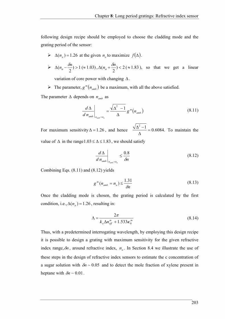
Chapter 8: Long period gratings: Refractive index sensor
203
following design recipe should be employed to choose the cladding mode and the
grating period of the sensor:
26.1)( an at the given an to maximize f .
1)2
( n
na
)03.1( , 2)2
( n
na
( 83.1 ), so that we get a linear
variation of core power with changing .
The parameter, ambm ng be a maximum, with all the above satisfied.
The parameter depends on ambn as
ambm
nnamb
ngnd
d
aamb
12
(8.11)
For maximum sensitivity 26.1 , and hence .6084.012
To maintain the
value of in the range 83.103.1 , we should satisfy
nnd
d
aamb nnamb 8.0
(8.12)
Combining Eqs. (8.11) and (8.12) yields
nnng aamb
m
31.1
)( (8.13)
Once the cladding mode is chosen, the grating period is calculated by the first
condition, i.e., 26.1)( an , resulting in:
mmeffo nk 0533.1
2
(8.14)
Thus, with a predetermined interrogating wavelength, by employing this design recipe
it is possible to design a grating with maximum sensitivity for the given refractive
index range, n , around refractive index, an . In Section 8.4 we illustrate the use of
these steps in the design of refractive index sensors to estimate the c concentration of
a sugar solution with 05.0~n and to detect the mole fraction of xylene present in
heptane with 01.0~n .
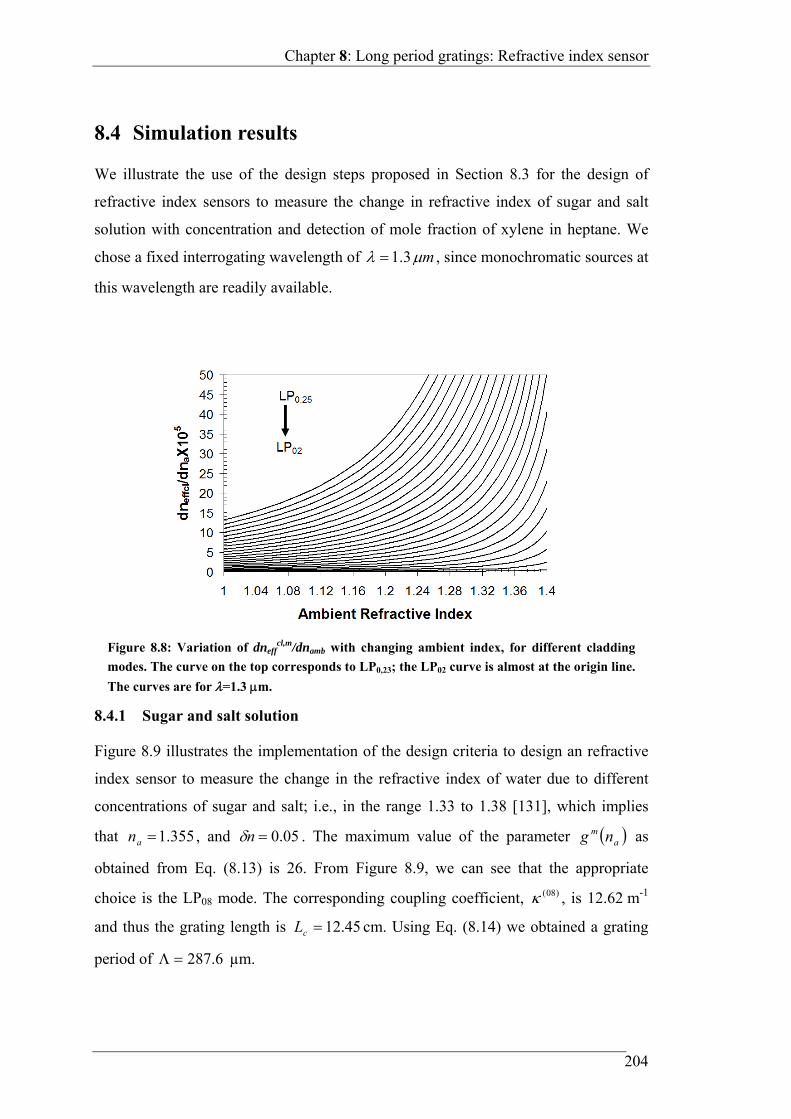
Chapter 8: Long period gratings: Refractive index sensor
204
8.4 Simulation results
We illustrate the use of the design steps proposed in Section 8.3 for the design of
refractive index sensors to measure the change in refractive index of sugar and salt
solution with concentration and detection of mole fraction of xylene in heptane. We
chose a fixed interrogating wavelength of m 3.1 , since monochromatic sources at
this wavelength are readily available.
8.4.1 Sugar and salt solution
Figure 8.9 illustrates the implementation of the design criteria to design an refractive
index sensor to measure the change in the refractive index of water due to different
concentrations of sugar and salt; i.e., in the range 1.33 to 1.38 [131], which implies
that 355.1an , and 05.0n . The maximum value of the parameter am ng as
obtained from Eq. (8.13) is 26. From Figure 8.9, we can see that the appropriate
choice is the LP08 mode. The corresponding coupling coefficient, )08( , is 12.62 m-1
and thus the grating length is 45.12cL cm. Using Eq. (8.14) we obtained a grating
period of 6.287 µm.
Figure 8.8: Variation of dneffcl,m/dnamb with changing ambient index, for different cladding
modes. The curve on the top corresponds to LP0,23; the LP02 curve is almost at the origin line.
The curves are for =1.3 m.
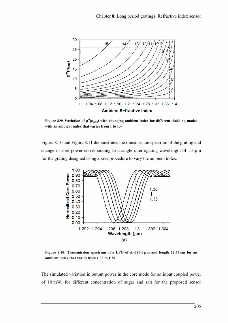
Chapter 8: Long period gratings: Refractive index sensor
205
Figure 8.10 and Figure 8.11 demonstrates the transmission spectrum of the grating and
change in core power corresponding to a single interrogating wavelength of 1.3 µm
for the grating designed using above procedure to vary the ambient index.
The simulated variation in output power in the core mode for an input coupled power
of 10 mW, for different concentration of sugar and salt for the proposed sensor
Figure 8.9: Variation of gm(namb) with changing ambient index for different cladding modes
with an ambient index that varies from 1 to 1.4
Figure 8.10: Transmission spectrum of a LPG of =287.6 m and length 12.45 cm for an
ambient index that varies from 1.33 to 1.38.
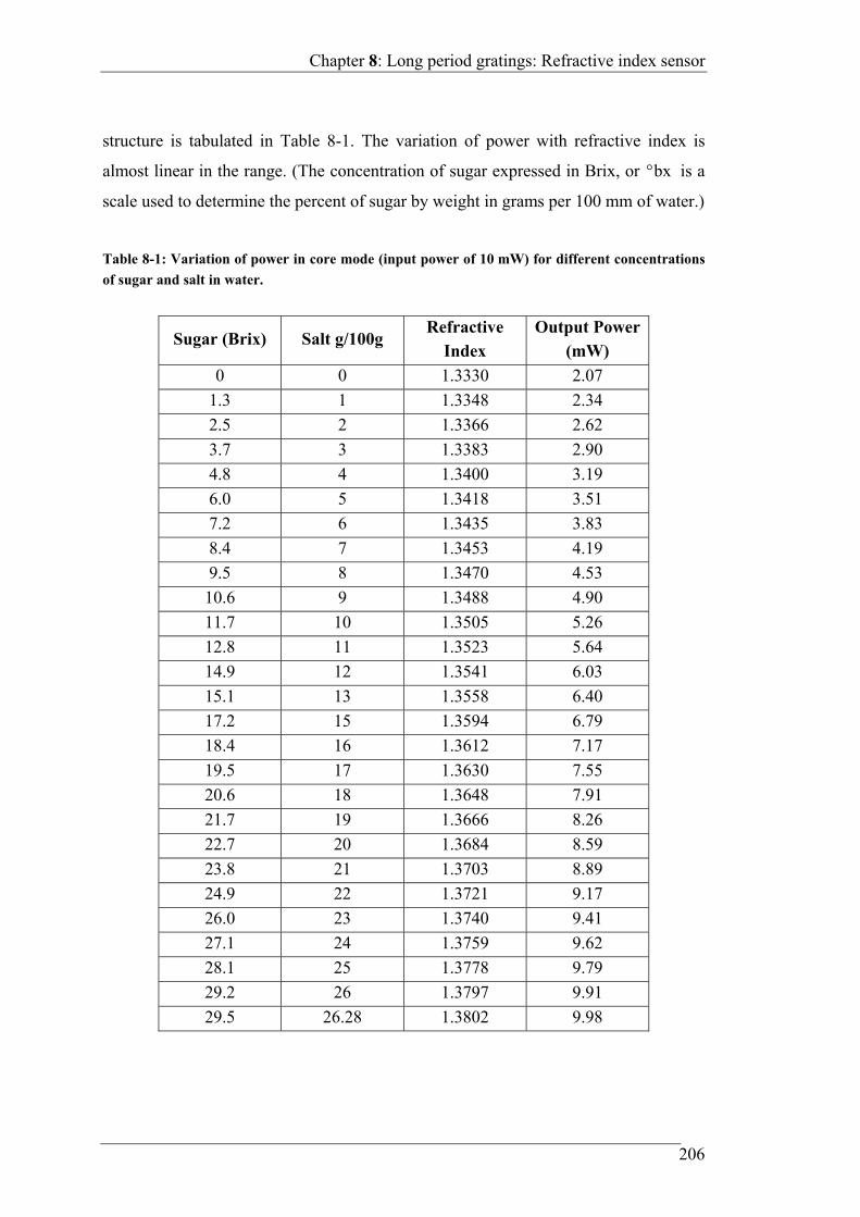
Chapter 8: Long period gratings: Refractive index sensor
206
structure is tabulated in Table 8-1. The variation of power with refractive index is
almost linear in the range. (The concentration of sugar expressed in Brix, or bx is a
scale used to determine the percent of sugar by weight in grams per 100 mm of water.)
Table 8-1: Variation of power in core mode (input power of 10 mW) for different concentrations
of sugar and salt in water.
Sugar (Brix) Salt g/100g Refractive
Index Output Power
(mW)
0 0 1.3330 2.07
1.3 1 1.3348 2.34
2.5 2 1.3366 2.62
3.7 3 1.3383 2.90
4.8 4 1.3400 3.19
6.0 5 1.3418 3.51
7.2 6 1.3435 3.83
8.4 7 1.3453 4.19
9.5 8 1.3470 4.53
10.6 9 1.3488 4.90
11.7 10 1.3505 5.26
12.8 11 1.3523 5.64
14.9 12 1.3541 6.03
15.1 13 1.3558 6.40
17.2 15 1.3594 6.79
18.4 16 1.3612 7.17
19.5 17 1.3630 7.55
20.6 18 1.3648 7.91
21.7 19 1.3666 8.26
22.7 20 1.3684 8.59
23.8 21 1.3703 8.89
24.9 22 1.3721 9.17
26.0 23 1.3740 9.41
27.1 24 1.3759 9.62
28.1 25 1.3778 9.79
29.2 26 1.3797 9.91
29.5 26.28 1.3802 9.98
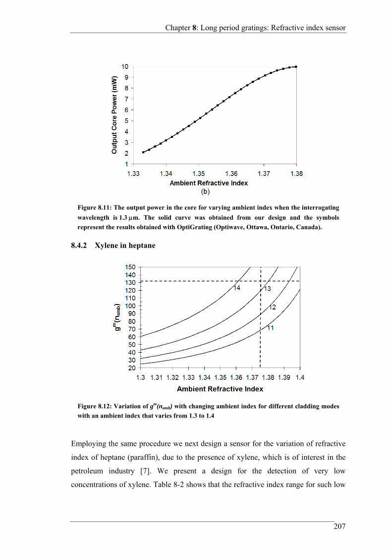
Chapter 8: Long period gratings: Refractive index sensor
207
8.4.2 Xylene in heptane
Employing the same procedure we next design a sensor for the variation of refractive
index of heptane (paraffin), due to the presence of xylene, which is of interest in the
petroleum industry [7]. We present a design for the detection of very low
concentrations of xylene. Table 8-2 shows that the refractive index range for such low
Figure 8.11: The output power in the core for varying ambient index when the interrogating
wavelength is 1.3 m. The solid curve was obtained from our design and the symbols
represent the results obtained with OptiGrating (Optiwave, Ottawa, Ontario, Canada).
Figure 8.12: Variation of gm(namb) with changing ambient index for different cladding modes
with an ambient index that varies from 1.3 to 1.4
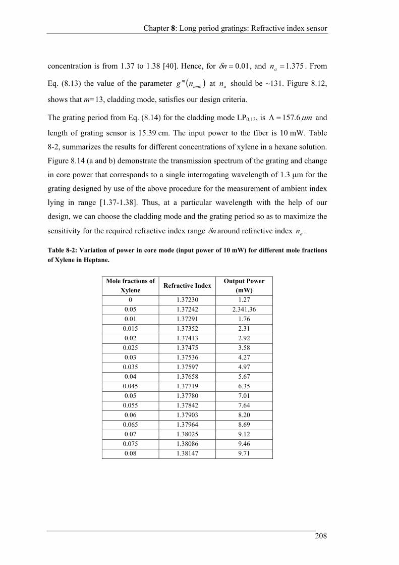
Chapter 8: Long period gratings: Refractive index sensor
208
concentration is from 1.37 to 1.38 [40]. Hence, for 01.0n , and 375.1an . From
Eq. (8.13) the value of the parameter ambm ng at an should be ~131. Figure 8.12,
shows that m=13, cladding mode, satisfies our design criteria.
The grating period from Eq. (8.14) for the cladding mode LP0,13, is m6.157 and
length of grating sensor is 15.39 cm. The input power to the fiber is 10 mW. Table
8-2, summarizes the results for different concentrations of xylene in a hexane solution.
Figure 8.14 (a and b) demonstrate the transmission spectrum of the grating and change
in core power that corresponds to a single interrogating wavelength of 1.3 µm for the
grating designed by use of the above procedure for the measurement of ambient index
lying in range [1.37-1.38]. Thus, at a particular wavelength with the help of our
design, we can choose the cladding mode and the grating period so as to maximize the
sensitivity for the required refractive index range n around refractive index an .
Table 8-2: Variation of power in core mode (input power of 10 mW) for different mole fractions
of Xylene in Heptane.
Mole fractions of
Xylene Refractive Index
Output Power (mW)
0 1.37230 1.27
0.05 1.37242 2.341.36
0.01 1.37291 1.76
0.015 1.37352 2.31
0.02 1.37413 2.92
0.025 1.37475 3.58
0.03 1.37536 4.27
0.035 1.37597 4.97
0.04 1.37658 5.67
0.045 1.37719 6.35
0.05 1.37780 7.01
0.055 1.37842 7.64
0.06 1.37903 8.20
0.065 1.37964 8.69
0.07 1.38025 9.12
0.075 1.38086 9.46
0.08 1.38147 9.71
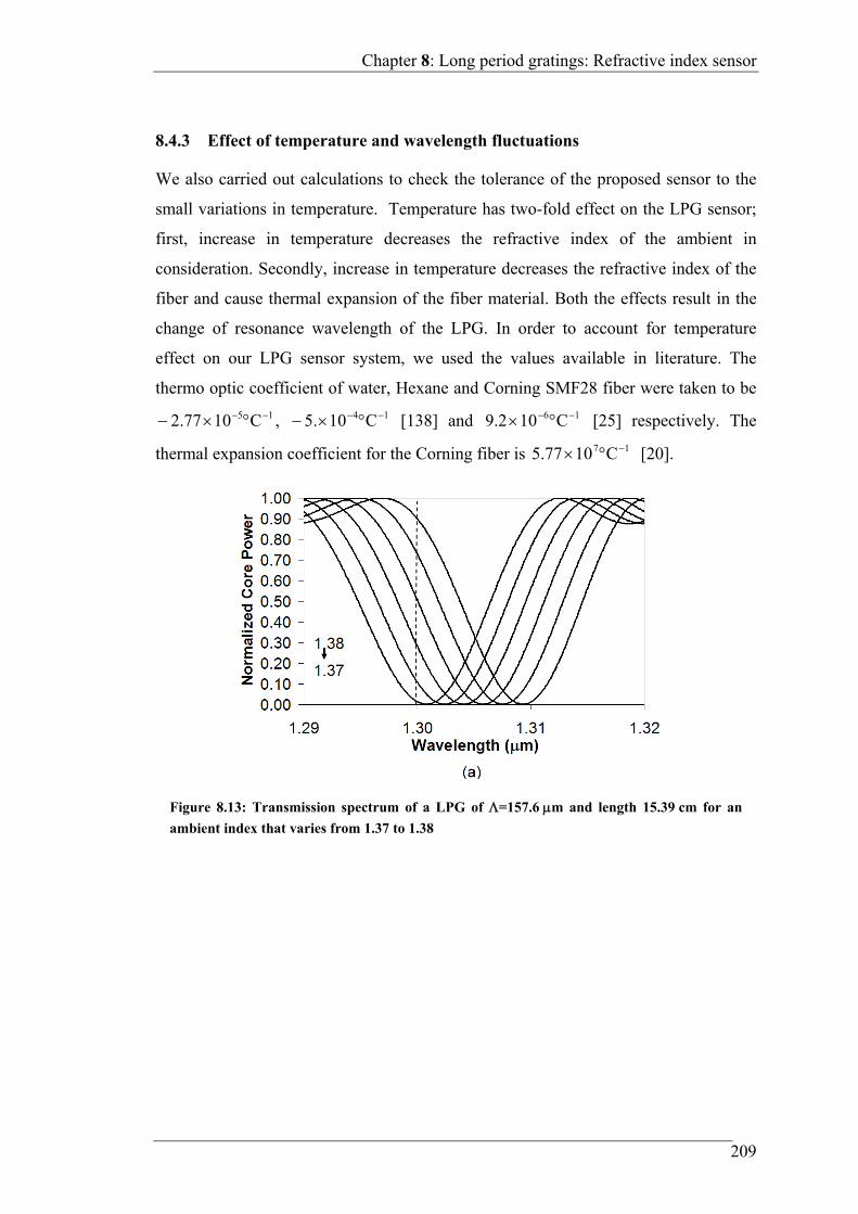
Chapter 8: Long period gratings: Refractive index sensor
209
8.4.3 Effect of temperature and wavelength fluctuations
We also carried out calculations to check the tolerance of the proposed sensor to the
small variations in temperature. Temperature has two-fold effect on the LPG sensor;
first, increase in temperature decreases the refractive index of the ambient in
consideration. Secondly, increase in temperature decreases the refractive index of the
fiber and cause thermal expansion of the fiber material. Both the effects result in the
change of resonance wavelength of the LPG. In order to account for temperature
effect on our LPG sensor system, we used the values available in literature. The
thermo optic coefficient of water, Hexane and Corning SMF28 fiber were taken to be
15 C1077.2 , 14 C10.5 [138] and 16 C102.9 [25] respectively. The
thermal expansion coefficient for the Corning fiber is 17 C1077.5 [20].
Figure 8.13: Transmission spectrum of a LPG of =157.6 m and length 15.39 cm for an
ambient index that varies from 1.37 to 1.38
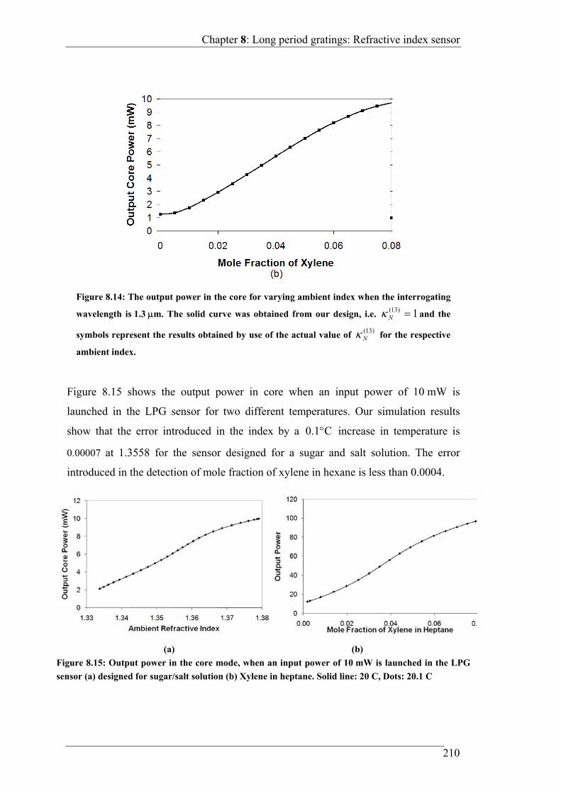
Chapter 8: Long period gratings: Refractive index sensor
210
Figure 8.15 shows the output power in core when an input power of 10 mW is
launched in the LPG sensor for two different temperatures. Our simulation results
show that the error introduced in the index by a C1.0 increase in temperature is
0.00007 at 1.3558 for the sensor designed for a sugar and salt solution. The error
introduced in the detection of mole fraction of xylene in hexane is less than 0.0004.
Figure 8.14: The output power in the core for varying ambient index when the interrogating
wavelength is 1.3 m. The solid curve was obtained from our design, i.e. 1)13( N and the
symbols represent the results obtained by use of the actual value of )13(N for the respective
ambient index.
(a) (b)
Figure 8.15: Output power in the core mode, when an input power of 10 mW is launched in the LPG
sensor (a) designed for sugar/salt solution (b) Xylene in heptane. Solid line: 20 C, Dots: 20.1 C
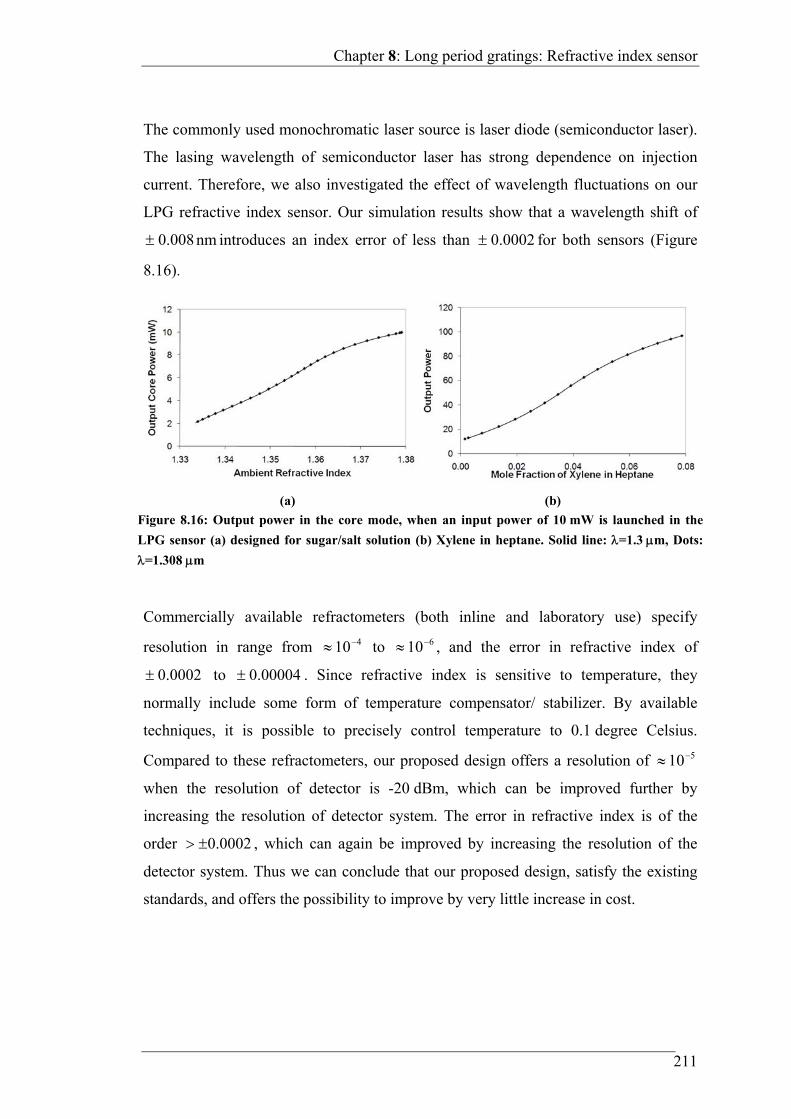
Chapter 8: Long period gratings: Refractive index sensor
211
The commonly used monochromatic laser source is laser diode (semiconductor laser).
The lasing wavelength of semiconductor laser has strong dependence on injection
current. Therefore, we also investigated the effect of wavelength fluctuations on our
LPG refractive index sensor. Our simulation results show that a wavelength shift of
nm008.0 introduces an index error of less than 0200.0 for both sensors (Figure
8.16).
Commercially available refractometers (both inline and laboratory use) specify
resolution in range from 410 to 610 , and the error in refractive index of
0002.0 to 00004.0 . Since refractive index is sensitive to temperature, they
normally include some form of temperature compensator/ stabilizer. By available
techniques, it is possible to precisely control temperature to 0.1 degree Celsius.
Compared to these refractometers, our proposed design offers a resolution of 510
when the resolution of detector is -20 dBm, which can be improved further by
increasing the resolution of detector system. The error in refractive index is of the
order 0002.0 , which can again be improved by increasing the resolution of the
detector system. Thus we can conclude that our proposed design, satisfy the existing
standards, and offers the possibility to improve by very little increase in cost.
(a) (b)
Figure 8.16: Output power in the core mode, when an input power of 10 mW is launched in the
LPG sensor (a) designed for sugar/salt solution (b) Xylene in heptane. Solid line: =1.3 m, Dots:
=1.308 m
Chapter 8: Long period gratings: Refractive index sensor
212
8.5 Summary
We have presented a detailed analysis for an LPG refractive index sensor based on the
detection of change in core power. A design was developed, to make the choice of
cladding mode and grating period with maximum sensitivity. The sensor can be
employed for the quality assurance of different fluids like water, milk, kerosene etc.
The LPG sensor has been demonstrated to measure changes in refractive index as low
as )10( 5 , which offers an attractive alternative to the existing high performance
liquid choromatograph and UV spectroscopy approaches used in oil refineries without
any loss of accuracy. The major advantage of such a LPG sensor is that it is robust,
inexpensive, compact and can be used for in situ measurements.
This work in parts has been reported in the following Publications:
E. K. Sharma, R. Singh and Amita Kapoor, Long Period Gratings: Design
and Applications, Technical Digest XXXIII Optical Society of India
Symposium 2007 on Optics and Optoelectronics, , organized by Tezpur
University in Association with Optical Society of India, 18-20th December,
(2007).
Amita Kapoor and E. K. Sharma, Long Period Grating Refractive Index
Sensor: Optimal Design For Single Wavelength Interrogation, Japan-Indo
Workshop on Microwaves, Photonics and Communication Systems, Kyushu
University, Fukuoka, Japan. Workshop Digest, July, (2008).
Amita Kapoor and E. K. Sharma, Long Period Grating Refractive Index
Sensor: Optimal Design For Single Wavelength Interrogation, Proc. of
Photonics, Delhi, India, December (2008).
E. K. Sharma, R. Singh, K. C. Patra and Amita Kapoor, Long Period
Gratings: Analysis and Applications, International Symposium on Microwave
and Optical Technology (ISMOT), 16-19 December (2009).
Amita Kapoor and E. K Sharma, Long Period Grating Refractive Index
Sensor: Optimal Design For Single Wavelength Interrogation, Applied Optics,
48(31), pp G88-G94, (2009).
Chapter 8: Long period gratings: Refractive index sensor
213
Scope for future work
In this thesis, we focused on the modeling and analysis of optical amplifiers
specifically EDFAs, EDWAs and SOAs. With the ever expanding internet and fiber to
the home technology becoming commercially viable the necessity of designing all
optical networks is increasing. This necessitates development of methods that allows
quick and at low cost design of optical amplifiers and optical signal processors.
The work presented in this thesis can be extended and consolidated along the
following lines:
Raman optical amplifiers based on stimulated Raman scattering which occurs in fiber
at high optical powers. Whereas an EDFA requires specially constructed fibers,
Raman amplification takes place in standard transmission fibers and can be distributed
across a length of the fiber. Since Raman gain in a particular spectral range is derived
from the SRS induced transfer of optical power from a shorter wavelength to a higher
wavelength, these amplifiers can be designed for use across the entire 1.26 m to
1.65 m band. It will be of interest to extend our methodologies used in EDFA and
EDWA for the analysis of such amplifiers.
ATLAS is a well established tool for Silicon based devices. Along with ATHENA, we
can use ATLAS to simulate design and characterize a silicon based device. Silicon
photonics is a fast growing technology. The procedure developed in this thesis for
modeling SOA with ATLAS can be extended to study the silicon based optical
amplifiers.
We have shown that the using a single interrogating wavelength we can design a
refractive index sensor with maximum sensitivity around a desired refractive index
range. The procedure should be investigated experimentally and extended to for multi-
parameter sensing.

Appendix A Bibliography
215
Appendix A Bibliography
1 Abramowitz, M., and Stegun, I. A. (1972) Handbook of Mathematical Function,
New York:Dover.
2 Adachi, S. (1992). Physical properties of III-V semiconductor compounds, John
Wiley & Sons.
3 Adams, M. J. (1981). An introduction to optical waveguide, Wiley, Chichester,
England.
4 Agrawal, G. P. (1995). Semiconductor lasers: Past, present and future,
Woodbury, NY: AIP Press, 244-248.
5 Agrawal, G. P. (2005). Lightwave Technology- Telecommunication System, John
Wiley & Sons.
6 Agrawal, G. P., and Dutta, N. K. (1986). Long wavelength semiconductor lasers,
Van Nostrand Reinhold.
7 Allsop, T., Zhang, L., and Bennion, I. (2001). “Detection of organic aromatic
compounds in paraffin by a long period grating optical sensor with optimized
sensitivity”, Optics Communications 191, 181-190.
8 Arregui, F. J., Matias, I. R., and Claus, R. O. (2004). “Fiber optic biosensors”,
Encylopedia of Opt. Engg.
9 Asyran, L. V. (2005). “Spontaneous radiative recombination and nonradiative
Auger recombination in quantum confined heterostructures”, Quantum
Electron”, 35(12), 1117-1120.
10 ATLAS user manual, year 2006.
11 Barnham, K., and Vvedensky, D. D. (2001). Low dimensional semiconductor
structures: fundamentals and device applications, Cambridge University Press.
12 Basu, P. K. (1997). Theory of optical Processes in Semiconductors: bulk and
Microstructures, Oxford University Press, 190-192.
13 Baumann, I., Brinkmann, R., Dinand, M., Sohler, W., and Westenhofer, S.
(1996). “Ti:Er:LiNbO3 waveguide laser of optimized efficiency,” IEEE J.
Quantum Electron. 32, 1695–1706.

Appendix A Bibliography
216
14 Bayart, D., Clesca, B., Hamon, L., and Beylat, J. L. (1994). “Experimental
investigation of the gain flatness characteristics for 1.55 m Erbium doped
Fluoride fiber amplifiers”, IEEE Photon. Tech. Lett., 6, 613-615.
15 Becker, P. C., Olsson, N. A., and Simpson, J. R. (1998). Erbium-Doped Fiber
Amplifiers, Academic Press.
16 Bendelli, G., Komori, K., and Arai, S. (1992). “Gain saturation and propagation
characteristics of index-guided tapered-waveguide traveling-wave
semiconductor laser amplifiers (TTW-SLA’s)”, IEEE J. Quant. Electron., 28(2),
447-458.
17 Bendelli, G., Komori, K., Arai, S., and Suematsu, Y. (1991). “A new structure
for high-power TW-SLA”, IEEE Photon. Technol. Lett., 3 (1), 42-44.
18 Bhatia, V. (1999). “Applications of long-period gratings to single and multi-
parameter sensing”, Optics Express, Vol 4, No 11, 457-466.
19 Bhatia, V., and Vengsarkar, A. M. (1996). “Optical fiber long-period grating
sensors”, Optics Letters, Volume 21, No 9, 692-694.
20 Bousonville, and M., Rausch, J. (2009). “Velocity of signal delay changes in
fiber optic cables”, Proceedings of DIPAC.
21 Boyd, R. W. (2003). Nonlinear Optics, pp 56-60, Academic Press, Elsevier.
22 Brinkmann, R., Baumann, I., Dinand, M., Sohler, W., and Suche, H. (1994). “Er-
doped single and double pass Ti:LiNbO3 waveguide amplifiers,” IEEE J. Quant.
Electron. 30, 2356–2360.
23 Brosson, P. (1994). “Analytic Model of a Semiconductor Optical Amplifier”, J.
Lightw. Technol., 12, 49-54.
24 Caccavale, F., Gonella, F., Caneva, G., and Mansour, L. (1996). “Iterative
simplex-finite difference method for the characterization of optical waveguides”,
Journal of Lightwave Technology, 14(8), 1825-1830.
25 Chang, S., Hsu, C. C., Huang, T. H., Chuang, W. C., Tsai, Y. S., Shieh, J. Y.,
and Leung, C. Y. (2000). “Heterodyne Interferometric Measurement of the
Thermo-Optic Coefficient of Single Mode Fiber”, Chinese J.of Physics, 38, 437-
442.
26 Chang, W. Sc. (2005). Principles of Lasers and Optics, Cambridge University
Press.
Appendix A Bibliography
217
27 Chen, X., Zhang, L., Zhou, K., Davies, E., Sugden, K., Bennion, I., Hughes, M.,
and Hine, A. (2007). “Real-time detection of DNA interactions with long-period
fiber-grating-based biosensor,” Opt. Lett. 32(17), 2541–2543.
28 Chiang, K. S., Chan, F. Y. M. and Ng, M. N. (2004). "Analysis of Two Parallel
Long Period Fiber Gratings,” J. Lightwave Technol. 22, 1358-1366.
29 Chiang, K. S., Liu, Y., Ng, M. N. and Dong, X., (2000). “Analysis of etched
long- period fiber grating and its response to external refractive index”, Electron.
Lett., 36, 966-967.
30 Connelly, M. J. (2001). “Wideband semiconductor optical amplifier steady state
numerical model”, IEEE J. Quantum Electron., 37(3), 439-447.
31 Connelly, M. J. (2002). Semiconductor optical amplifiers, Kluwer Academic
Press.
32 Corning Incorporated, “Corning SMF28e Optical fiber product information”,
http://www.corning.com/assets/0/433/573/583/09573389-147D-4CBC-B55F-
18C817D5F800.pdf.
33 Della Valle, G., Sorbello, G., Festa, A., Taccheo, S., and Ennser, K. (2006).
”High-Gain Erbium-doped Waveguide Amplifier for Bidirectional Operation”,
ECOC 2006, 1-2.
34 Desurvire, E. (1994). Erbium Doped Fiber Amplifiers, John Wiley, New York.
35 Desurvire, E., Simpson, J. R., and Becker, P. C. (1987). "High gain erbium
doped travelling-wave amplifier," Opt. Lett. 12, 880-890.
36 Desurvire, E., Zyskind, J. L., and Simpson, J. R. (1990). "Spectral gain hole
burning at 1.53 m in Erbium Doped Fiber Amplifiers", IEEE Photonics Tech.
Lett., 2, 246.
37 Desuvire, E., Giles, C. R., and Simpson, J. R. (1989). “Gain saturation effects in
high speed multichannel erbium doped fiber amplifiers at =1.53 m,” IEEE J.
Lightwave Technol., 7(12), 2095-2104.
38 Deutsches Patent DBP Nr. 1254513, 1966. French Pat. Nr. 1548972; Brit. Pat.
Nr. 1202418; US Pat. Nr. 3845-293
39 Dinand, M., and Sohler, W. (1994). “Theoretical modeling of optical
amplification in Er-doped Ti:LiNbO3 waveguides”, IEEE J. of Quantum
Electron., 30(5), 1267-1276.
Appendix A Bibliography
218
40 Dominguez Perez, M., Segade, L., Ocabeza, C., Franjo, C., and Jimenze, E.
“Densities, Surface Tensions, and Refractive Indices of Propyl
Propanate+Hexane+m-Xylene at 298.15 K”, Journal of Chemical Engineering,
51(1), 294-300.
41 Donnelly, J. P., Walpole, J. N., Betts, G. E., Groves, S. H., Woodhouse, J. D.,
O'Donnell, F. J., Missaggia, L. J., Bailey, R. J., and Napoleone, A. (1996). “High
power 1.3 m InGaAsP-InP amplifiers with tapered gain regions”, IEEE Photon.
Technol. Lett., 8(11), 1450-1452.
42 Dutta, N. K., and Wang, Q. (2006). Semiconductor optical amplifier, World
Scientific.
43 Einstein, A. (1917). “Zur Quantentheorie der Strahlung”, Physikalische
Zeitschrift, Band 18, 121-128.
44 Erdogan, T. (1997). “Cladding mode resonances in short- and long-period fiber
grating filters”, J. Opt Soc. Am, A14 , 1760-1773.
45 Erdogan, T. (1997). “Fiber Grating Spectra”, J. Lightwave Technolgy, 15(8),
1277-1294.
46 Gabrielyan, V. T., Kaminskii, A. A., and Li, L. (1970). “Absorption and
Luminescence spectra and energy levels of Nd3+ and Er3+ ions in LiNbO3
crystals”, Phys. Stat. Sol. (a), 3, K37-K42.
47 Ghatak, A. K., and Thyagrajan, K. (1989). Optical Electronics, Cambridge
University Press.
48 Ghatak, A. K., and Thyagrajan, K. (2004). Introduction to Fiber Optics,
Cambridge University Press.
49 Giles, C. R. (1997). “Lightwave applications of fiber Bragg gratings”, J.
Lightwave Technol., 15(8), 1391-1404.
50 Girardin, F., Guekos, G., and Houbavlis, A. (1998). “Gain recovery of bulk
semiconductor optical amplifiers”, IEEE Photon. Tech lett, vol 10 (6), 784-786.
51 Greene, P. D., Rourke, and H. N. (1999). "Tailoring long period optical fiber
gratings for flattening of EDFA gain spectra," Elect. Lett. 35, 1375-1376.
52 Griffiths, G. J., and Esdaile, R. J. (1984). “Analysis of Titanium Diffused Planar
Optical Waveguides in Lithium Niobate”, IEEE J. of Quant. Electron.,20(2),
149-159.
Appendix A Bibliography
219
53 Hall, K. L., Lenz, G., Darwish A. M., and Ippen, E. P. (1994). “Subpicosecond
gain and index nonlinearities in InGaAsP diode lasers”, Optics Communications,
111, 589-612.
54 Hamaguchi, C. (2010). Basic Semiconductor Physics, Springer-Verlag.
55 Haug, A. (1985).“Influence of doping on threshold current of semiconductor
lasers”, Electron. Lett., 21(18), 792-794.
56 Henry, C. H. (1982). “Theory of the linewidth of semiconductor lasers”, IEEE J.
Quantum Electron., 18, 259-264.
57 Hill, K. O., Fujii, Y., Johnson, D. C., and Kawasaki, B. S. (1978).
"Photosensitivity in optical fiber waveguides: Applications to reflection filter
fabrication," Appl. Phy. Lett. 32(10), 647.
58 Hill, K. O., and Meltz, G. (1997). “Fiber Bragg grating technology fundamentals
and overview”, J. Lightw. Technol., 15(8), 1263-1276.
59 Hocker, G. B,. and Burns, W. K. (1977). “Mode dispersion in diffused channel
waveguides by the effective index method”, Appl. Optics, 16(1), 113-118.
60 Jain, G., and Sharma, E. K. (2004). “Gain calculation in erbium doped LiNbO3
channel waveguides by defining a complex index profile,” Opt. Eng.
(Bellingham) 43, 1454–1460.
61 Jain, G., Taneja, A. K., and Sharma, E. K. (2004). “Closed form modal field
expressions in diffused channel waveguides,” Proc. SPIE 5349, 163-171.
62 Kahen, K. (1988). “Two dimensional simulation of laser diodes in the steady
state”, IEEE Quantum Electron., 24(4), 641-651.
63 Kaminow, I. P., and Carruthrs, J. R. (1973). “Optical waveguiding layers in
LiNbO3 and LiTaO3”, Appl. Phys. Lett., 22(7), 326-328.
64 Kao, C. K., and Hockham, G. A. (1966). “Dielectric fiber surface waveguides
for optical frequencies”, IEE Proc., 133, 1151-1158.
65 Kapoor, A., Sharma, E. K., Freude, W., and Leuthold, J. (2010). “Investigation
of the saturation characteristics of InGaAsP-InP bulk SOA”, Proc. SPIE 7597,
75971I.
66 Kashyap, R. (1999). Fiber Bragg Gratings, Academic Press, London.

Appendix A Bibliography
220
67 Kashyap, R., Wyatt, R., and Campbell, R. J. (1993). "Wideband gain flattened
erbium doped fiber amplifiers using a blazed grating," Electron. Lett. 24, 154-
156.
68 Keiser, G. (2000). Optical Fiber Communications, 3rd edition Mc Graw Hill.
69 Kenyon, A. J., (2002). “Recent Developments in Rare-Earth Doped Materials for
Optoelectronics”, Progress in Quantum Electronics, 26(4-5), 225-284.
70 Kim, D. W., Zhang, Y., Cooper, K. L., and Wang, A. (2006). “Fiber-optic
interferometric immuno-sensor using long period grating,” Electron. Lett. 42(6),
324–325.
71 Kim, H. S., Yun, S. H., Kim, H. K., Park, N., and Kim, B. Y. (1998). ''Actively
gain-flattened erbium doped fiber amplifier over 35 nm by using all fiber
acousto-optic tunable filters, '' IEEE Photonics Technol. Lett. 10(8), 790-792.
72 Kim, I., Uppal, K., and Dapkus, P. D. (1998). “Gain saturation in traveling-wave
semiconductor optical amplifiers”, IEEE J. Quantum Electron., 34(10), 1949-
1952.
73 Klingshirn, C. F. (2005). Semiconductor Optics, 2nd Edition, pp 123-128,
Springer.
74 Koester, C. J., and Snitzer, E. (1964). “Amplification in a fiber laser”, Appl.
Optics 3 (10), 1182-1186.
75 Kononenko, A. K., Kononenko, K. I., and Mikhov, D. M. (1969).“Dependence
of refractive index on physiological state of microbial population”, Journal of
Applied Spectroscopy, 11(1), 795-797.
76 Lasher, G., and Stern, F. (1964). “Spontaneous and Stimulated Recombination
radiation in Semiconductors”, Physical Review, 133(2A), A553-A563.
77 Leuthold, J. (1998). Advanced Indium-Phosphide waveguide Mach-Zehnder
interferometer all-optical switches and wavelength converters, Dissertation,
Zurich.
78 Li, M. J. (1988). "Optical waveguide fabrication in neodymium-doped lithium
niobate", Electronics Lett., 24(15), 914-915.
79 Lu, Y. B., and Chu, P. L. (2000). "Gain flattening by using dual core fiber in
erbium doped fiber amplifier,” IEEE. Photonics Technol. Lett. 12, 1616-1618.
Appendix A Bibliography
221
80 Marcatili, E. A. J., (1969). “Dielectric rectangular waveguide and directional
coupler for integrated optics”, Bell Syst. Tech. J., 48(7), 2071-2102.
81 Marcuse, D. A. (1983). “Computer model of an injection laser amplifier”, IEEE
J. Quantum Electron., QE-19, 63-73.
82 März, R., (1995). Integrated optics: design and modeling, Artech House
Publishers.
83 Mears, R .J., Reekie, L., Jauncey, I. M., and Payne, D.N. (1987). "Low noise
erbium fiber amplifier operating at 1.3m," Electon. Lett, 23, 1026-1028.
84 Mears, R. J., Reekie, L., Poole, S. B., and Payne, D.N. (1986). "Low threshold,
tunable cw and Q switched fiber laser operating at 1.55 m," Electon. Lett,
22,159-160.
85 Meccozi, A., and Mørk, J. (1997). “Saturation effects in nondegenerate four
wave mixing between short optical pulses in semiconductor laser amplifiers”,
IEEE J. Selected Topics Quantum Electron., 3(5), 1190-1207.
86 Melnik, S., Huyet, G., and Uskov, A. V. (2006). “The linewidth enhancement
factor of quantum dot semiconductor lasers”, Optics express, 14(7), 2950-
2955.
87 Meltz, G., Morey, W. W., and Glenn, W. H. (1989). "Formation of Bragg
gratings in optical fibers by transverse holographic method," Opt. Lett. 14(15),
823-825.
88 Meyer, G. E., Novielli, K. A., and Smith, J. E. (1987). “Use of refractive index
measurement for quality assurance of pediatric parenteral nutrient solutions”,
American J. of Hospital Pharmacy, 44(7), 1617-1620.
89 Monerie, M. (1982). “Propagation in doubly clad single mode fibers”, IEEE
Trans Microwave Theory Tech 30, 381-388.
90 Morito, K., Tanaka, S., Tomabechi, S., and Kuramata, A. (2005). “A broad-band
MQW semiconductor optical amplifier with high saturation output power and
low noise figure”, IEEE Photon. Technol. Lett., 17(5), 974-976.
91 Mørk, J., Nielsen, M. L., and Berg, T. W. (2003). “The dynamics of
semiconductor optical amplifiers: modeling and applications”, Opt. Photon.
News, 14(7), 43-48.
Appendix A Bibliography
222
92 Ng, W., and Liu, Y. Z. (1980). “Effect of p-doping on carrier lifetime and
threshold current density of 1-3 m GaInAsP/InP lasers by liquid-phase
epitaxy”, Electron. Lett., 16 (18), 693-695.
93 Nilsson, N. G. (1978). “Empirical approximations for the Fermi energy of a
semiconductor with parabolic bands”, Appl. Phys. Lett., 33, 653-654.
94 Occhi, L., (2002). Semiconductor optical amplifiers made of ridge waveguide
bulk InGaAsP/InP: Experimental characterisation and numerical modelling of
gain, phase, and noise, Dissertation, Zurich.
95 Patra, K. C., Singh, R, and Sharma, E. K. (2010), “Analysis of transmission
characteristics of long period gratings in tapered optical fibers”, Appl. Opt.,
48(31), G95-G100.
96 Patrick, H. J., Kersey, A. D., and Bucholtz, F. (1998). “Analysis of the response
of Long Period Fiber Gratings to External Index of refraction”, J. Lightwave
Technology, 16(9), 1606-1612.
97 Pilla, P., Manzillo, P. F., Malachovska, V., Buosciolo, A., Campopiano, S.,
Cutolo, A., Ambrosio, L., Giordano, M., and Cusano, A. (2009). ” Long period
grating working in transition mode as promising technological platform for label
free biosensing”, Opt. Express, 17 (22).
98 Pleumeekers, J. L., Kauer, M., Dreyer, K., Burrus, C., Dentai, A. G., Shunk, S.,
Leuthold, J., and Joyner, C. H. (2002). “Acceleration of gain recovery in
semiconductor optical amplifiers by optical injection Near Transparency
Wavelength”, IEEE Photon. Technol. Lett., 14(1), 12-14.
99 Prat J. (2008). Next Generation FTTH Passive Optical Networks- Research
towards unlimited bandwidth access, Springer Science.
100 Press, W. H., Teukolsky, S. A., Vetterling, W. T., and Flannery, B. P. (1995).
Numerical recipes in C: The art of scientific computing, Cambridge University
Press.
101 Prudnikov, A. V., Brychkv, Y. A., and Marichev, O. I. (1986). Integrals and
Series, Gorden and Breach Science Publisher, Amsterdam, The Netherland.
102 Qasaimeh, O. (2009). “Effect of doping on the optical characteristics of
quantum-dot semiconductor optical amplifiers”, J. Lightw. Technol., 27(12),
1978-1984.
Appendix A Bibliography
223
103 Rahman, B. M. A. (1995). “Finite element analysis of optical waveguides”,
Progress in Electromagnetics Research, PIER 10, 187-216.
104 Rahman, B. M. A., Fernandez, F. A., and Davies, J. B. (1991). “Review of finite
element methods for microwave and optical waveguides”, Proceedings of the
IEEE, 79(10), 1442-1448.
105 Rappaza, B., Barbulb, A., Charrièrec, F., Kühnc, J., Marquetd, P., Korensteinb,
R., Depeursingec, V, and Magistrettia, P. (2007). “Erythrocytes volume and
refractive index measurement with a Digital Holographic Microscope”, Proc.
SPIE 6445, 644509.
106 Rego, G. M., Santos, J. L., and Salgado, H. M. (2006). “Refractive Index
measurement with long-period gratings arc-induces in pure silica-core fibers”,
Optics Communications, 259(2), 598-602.
107 Rochelle, M., Guy, M., Lauzon, J., and LaRochelle, S. (1999). ''Gain
Equalization of EDFA’s with Fiber Bragg Gratings, '' Photon. Technol. Lett. 11,
1343-1345.
108 Rosencher, E., and Vinter, B. (2002). Optoelectronics, Translation by Piva, P. G.
Cambridge University Press.
109 Sakamoto, T., Aozasa, S., Yamada, M., and Shimizu, M. (2003). “High-gain
hybrid amplifier consisting of cascaded fluoride-based TDFA and silica-based
EDFA in 1458–1540nm wavelength region”, IEEE Electronics Lett., 39(7), 597-
599.
110 Saleh, B. E. A., and Teich, M. C. (2007). Fundamental of Photonics, John Wiley
& Sons.
111 Scarborough, J. B. (1966). Numerical Mathematical Analysis, U.S.A: The John
Hopkins Press.
112 Sharma, A., and Bindal, P. (1992). “An accurate variational analysis of single
mode diffused channel waveguides”, Optical and Quantum Electron., 24, 1359-
1371.
113 Sharma, A., and Bindal, P. (1993). “Analysis of Diffused Planar and Channel
Waveguides,” IEEE J. of Quantum Electron.,29, 150-153.

Appendix A Bibliography
224
114 Sharma, E. K., Srivastava, S., and Meunier, J. P. (1996). “Mode coupling
analysis for the design of refractive ion exchange integrated optical
components”, IEEE J. Selected Topics Quantum Electronics, 2(2), 165-173.
115 Shu, X., Zhang, L., and Bennion, I. (2002).“Sensitivity Characteristics of Long
Period Fiber Gratings”, J. Lightwave Technology, Vol 20, No. 2, 255-266.
116 Shulika, O., Freude, W., and Leuthold, J. (2007). “Two dimensional simulation
of semiconductor lasers and semiconductor optical amplifiers using ATLAS”,
Optoelectronic Physics and Technology, 2007. OPT '07. International Workshop
on , 34-38.
117 Singh, R., Kumar, H., and Sharma, E. K. (2003). “Design of Long Period
Gratings necessity of a three layer fiber geometry for cladding mode
characteristics”, Microwave and Optical Techno. Lett, 37(1), 45-49.
118 Singh, R., and Sharma, E. K. (2007). “Tailoring the transmission spectrum of the
long period fiber gratings by variation in the length of the grating”, Proc. SPIE,
6468, 646808.
119 Singh, R., Sunanda, and Sharma, E. K. (2004). “Gain Flattening by Long Period
Gratings Designed in Erbium Doped Fibers”, Optics Comm., 240,123-132.
120 Snitzer, E., and Woodcock, R. (1965). “Yb3+-Er3+ glass laser”, Appl. Phys. Lett.,
6(3), 45-46.
121 Snyder, A. W. (1972). “Coupled mode theory for optical fiber,” J. Opt. Soc.
Amer., 62, 1267-1277.
122 Snyder, A. W., and Love, J. D. (2000). Optical Waveguide Theory, Kluwer
Academic Publishers.
123 Springer Materials, The Landoelt-Bornstein database,
http://www.springermaterials.com/navigation/.
124 Su, C. B., and Lanzisera, V. (1984). “Effect of doping on the gain constant and
modulation bandwidth of InGaAsP semiconductor lasers”, Appl. Phys. Lett.,
45(12), 1302-1304.
125 Sunanda, Jain, G., and Sharma, E. K. (2001). “Gain calculations in erbium-
doped fibers using field approximations”, Microwave and Opt. Techno. Lett.,
29(4), 256-259.
Appendix A Bibliography
225
126 Sze, S. M., and d Ng, K. K. (2007). Physics of semiconductor devices, Third
edition, John Wiley and Sons.
127 Taccheo, S., Valle, G. D., Festa, A., and Ennser, K. (2007). “Gain-Stabilized
Erbium-Doped Waveguide Amplifier for Burst Transmission”, IEEE. Photonics
Technol. Lett. 19, 97-99.
128 Tamir, T., and Alferness, R. C. (1988). Guided-wave Optoelectronics, Springer-
Verlag.
129 Taneja, A. K., Srivastava, S., and Sharma, E. K. (1997). “Closed form
expression for propagation characteristics of diffused planar optical
waveguides,” Microwave Opt. Technol. Lett. 15, 305–310.
130 Thyagrajan, K., and Ghatak, A. K. (2007). Fiber optic essential, John Wiley &
Sons.
131 Topac Incorporated, “Relationship between salt solution and sugar concentration
(Brix) and refractive index at C20 ”, www.topac.com/salinity_brix.html.
132 Tycko, D. H., Mete, M. H., Epstein, E. A., and Grinbaum, A. (1985). “Flow-
Cytometric Light Scattering measurement of red blood cells volume and
hemoglobin concentration”, Appl. Opt. 24 (9), 1355-1365.
133 Vasileska, D., and Goodnick, S. M. (2006). Computational Electronics, Morgan
and Claypool Publishers.
134 Vengaskar, A. M., Lemaire, P. J., Judkins, J. B., Bhatia, V., Erdogan, T., and
Sipe, J. E. (1996). “Long Period fiber gratings as band rejection filters”, J.
Lightwave Technology, 14(1), 58-64.
135 Verdeyen, J. T. (1981). Laser Electronics, Prentice Hall.
136 Wang, J., Maitra, A., Poulton, C. G., Freude, W., and Leuthold, J. (2007).
“Temporal dynamics of the alpha factor in semiconductor optical amplifiers”, J.
Lightw. Technol., 25(3), 12-14.
137 Wang, Z., Heflin, J. R., Van Cott, K., Stolen, R. H., Ramachandran, S., and
Ghalmi, S. (2009). “Biosensors employing ionic self-assembled multilayers
adsorbed on long-period fiber gratings,” Sens. Actuators B Chem. 139(2), 618–
623.
138 Weast, R. C. ed., (1982). The Handbook of Physics and Chemistry, CRC Press.

Appendix A Bibliography
226
139 Wiesenfeld, J. M. (1996). “Gain dynamics and associated nonlinearities in
semiconductor optical amplifiers”, J. High Speed Electronics and Systems, 7(1),
179-222.
140 Wilcox, J. Z., Peterson, G. L., Ou, S., Yang, J. J., Jansen, M., and Schechter, D.
(1988). “Gain and threshold-current dependence for multiple quantum-well
lasers”, J. Appl. Phys., 64, 6564–6567.
141 Willardson, R. K., Beer, A. C., Tsang, W. T., and Pankove, J. I. (1985).
Semiconductors and semimetals, 22, 172-175, Academic Press London.
142 Wolff, P. A. (1962). “Theory of the band structure of very degenerate
semiconductors”, Physics Review, 126, 405-412.
143 Wysocki, P. F., Judkins, J. B., Espindola, R. P., Andejco, M., and
Vengsarkar, A. M. (1997). "Broad-band erbium–doped fiber amplifier flattened
beyond 40 nm using long period grating filter," Photon Technol. Lett. 9, 1343-
1345.
144 Yu, P. Y., Cardona, M. (2005). Fundamentals of Semiconductors, 3rd edition,
Springer, 306-311.
145 Zhang, L., Kang, I., Bhardwaj, A., Sauer, N., Cabot, S., Jaques, J., and Neilson,
D. T. (2006). “Reduced recovery time semiconductor optical amplifier using p-
type-doped multiple quantum wells”, IEEE Photon. Technol. Lett., 18(22),
2323-2325.
146 Zhu, T., Rao, Y. J., and Mo, Q. J. (2005). “Simultaneous measurement of
Refractive Index and Temperature using a single ultralong-Period fiber grating”,
IEEE Photonics Techno. Lett, 17(12), 1118-1120.
147 Zory, P. S. (1993). Quantum well lasers, Academic Press, San Diego, California.
Appendix B Modified Coupled Mode Analysis
227
Appendix B Modified Coupled Mode Analysis
In order to consider the LPG written in an EDF the reformulated the coupled mode
analysis is presented here [118]. The analysis includes an extraneous attenuation
factor for the cladding mode. The modified total field at any wavelength j can be
written as:
zim,jclj
zijcoj
j m,jcl
jco ezBezA
where jco and j
co represents the normalized modal field and propagation constant
of the core mode of the EDF, and m,jcl and m,j
cl represents the normalized modal
field and propagation constant of the cladding guided mode of the fiber for the
wavelength j. The propagation constant jco , is complex, i.e., zi j
jco
jco ,
where zj is the corresponding gain coefficient and is the extraneous scattering
loss. It is assumed that the cladding modes do not experience any gain. The modal
fields jco , and m,j
cl satisfy the Helmholtz equations. The total field satisfies the
following wave equation:
02222
22
j
j
jj
t znnkz
Substituting the field expression for j in the wave equation and using the slowly
varying approximation we get:
Appendix B Modified Coupled Mode Analysis
228
0
22
222
m,
,
m,22
,,2,
22
zijclj
zijcojj
zimjclj
mjclj
jmjcl
zijcoj
jco
jcoj
jco
jco
jco
jjco
jco
jcl
jco
mjcl
jco
ezBezAznk
eBiBdz
dBi
eAziAzzdz
dAzi
Since zi jj
coj
co , and only the gain coefficient j is a function of z, therefore
jj
co i and jj
co i . The term j is small in comparison, it can be neglected.
0
22
22222
m,
,
m,22
,,2,
22
zijclj
zijcojj
zzimjclj
mjclj
jmjcl
zijcojjjjjj
jcoj
jjj
jco
jcl
jco
mjcl
jco
ezBezAznk
eeBiBdz
dBi
eAzzzizdz
dAziii
Simplifying, we get:
zi
eBeKzsine
zi
Azzziz
dz
dA
jjj
co
zj
zjj
zi
jjj
co
jjjjjj
cojjjj
2
4
2
2122 12122
m,jcl
zj
zjm,jcl
zi
m,jcl
jjm,j
clj
i
eAeKzsine
i
Bi
dz
dB jj
2
4
2
2 212
In the above equations m,jcl
jcoj , j
12 and j21 are the coupling coefficients
for wavelength j. 2K , s the grating period and satisfies the phase matching
condition 2 j for coupling to a particular cladding mode at wavelength j.
If we define new amplitudes zjj eAA and z
jj eBB . The power carried by
the core mode and the cladding mode at any length z can hence, be expressed as
2jA and
2jB respectively and the coupled equations reduce to:
Appendix B Modified Coupled Mode Analysis
229
jjj
jjj
co
jjj
cozi
jjj
co
jjjjj
cojjAz
zi
BKzsine
zi
Azzziz
dz
Ad j
2
4
2
2122 1222
jm,jcl
jzjm,j
clzi
m,jcl
jm,j
cljB
i
AeKzsine
i
Bi
dz
Bd jj
2
4
2
2 212

Appendix C Optical and Electrical Parameters for Indium Gallium Arsenide Phosphate
231
Appendix C Optical and Electrical Parameters for Indium Gallium Arsenide Phosphate
If x and y composition fraction are known we can find out different material
parameters from the expressions given below [10, 2,123].
The bandgap energy:
159.0109.028.0101.1101.0758.0642.035.1)eV( yxxyyyxxWg
Spin-orbit splitting energy:
2107.03.0119.0)eV( yySO
Effective mass of electron:
0* 309.0080.0 myme
Effective mass of heavy holes:
0* 14.045.0145.079.01 mxxyxxymhh
Effective mass of light holes:
0* 1026.008.0112.014.01 mxxyxxymlh
Dielectric constant:
xxyxxy 12.121.1316.94.81
Conduction band offset for lattice matched InP-InGaAsP interface:
2003.0268.0)eV( yWC
Here m0 is the rest mass of an electron.

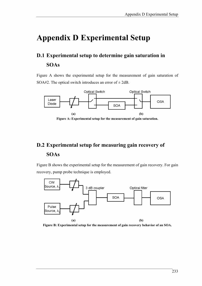
Appendix D Experimental Setup
233
Appendix D Experimental Setup
D.1 Experimental setup to determine gain saturation in
SOAs
Figure A shows the experimental setup for the measurement of gain saturation of
SOA#2. The optical switch introduces an error of ± 2dB.
D.2 Experimental setup for measuring gain recovery of
SOAs
Figure B shows the experimental setup for the measurement of gain recovery. For gain
recovery, pump probe technique is employed.
(a) (b)
Figure A: Experimental setup for the measurement of gain saturation.
(a) (b)
Figure B: Experimental setup for the measurement of gain recovery behavior of an SOA.


Publications


Long period grating refractive-index sensor: optimaldesign for single wavelength interrogation
Amita Kapoor1,3 and Enakshi K. Sharma2,*1Shaheed Rajguru College of Applied Sciences for Women, University of Delhi, Delhi 110095, India
2Department of Electronic Science, University of Delhi South Campus, New Delhi 110021, India3Currently with the Institute of Photonics and Quantum Electronics, University of Karlsruhe,
Engesserstrasse 5, Karlsruhe 76131, Germany
*Corresponding author: [email protected]
Received 16 June 2009; revised 12 September 2009; accepted 13 September 2009;posted 15 September 2009 (Doc. ID 112870); published 7 October 2009
We report the design criteria for the use of long period gratings (LPGs) as refractive-index sensors withoutput power at a single interrogating wavelength as the measurement parameter. The design givesmaximum sensitivity in a given refractive-index range when the interrogating wavelength is fixed.Use of the design criteria is illustrated by the design of refractive-index sensors for specific applicationto refractive-index variation of a sugar solution with a concentration and detection of mole fraction ofxylene in heptane (paraffin). © 2009 Optical Society of America
OCIS codes: 120.0120, 230.2285.
1. Introduction
The standard method of measuring the refractive in-dex is to use an Abbe refractometer, which generallyinvolves sending the sample to a laboratory, a costly,time-consuming process that is not susceptible toreal-time monitoring. Therefore, it is natural toconsider the utilization of optical fiber technologyto measure the refractive index because of its uniquecharacteristics such as ease of fabrication, low inser-tion loss, high sensitivity, fast response, and com-pactness. More specifically, long period gratings(LPGs) have been used as sensors for various physi-cal properties such as strain, temperature, and re-fractive index.A LPG couples the power from the forward propa-
gating core mode to the copropagating claddingmodes. The cladding modes can be easily attenuated,and this results in the transmission spectrum of thefiber containing a series of attenuation bands cen-tered at discrete wavelengths, with each attenuation
band corresponding to the coupling to a differentcladding mode [1–5]. A specific feature of LPGs isthe sensitivity of the transmission spectrum to therefractive index of ambient namb, i.e., the materialthat surrounds the cladding of fiber [6,7] becausethe effective indices of the cladding modes, ncl;m
eff , arestrongly influenced by the ambient refractive index.The primary effect of change in the ambient refrac-tive index is the consequent change in resonantwavelength. Hence, several authors have exploitedthis feature of a LPG to implement refractive-indexsensors based on the change in resonant wavelength[1,8,6,7,9], i.e., they measure the small shift in theresonant wavelength with a change in ambient re-fractive index. The limitation of this technique isthat the measurement of such small wavelengthshifts requires the use of relatively expensive high-resolution optical spectrum analyzers (OSAs).
We present an alternative approach for measure-ment of the refractive index using a LPG. In ourmethod a LPG is interrogated by a single wavelengthsource and, instead of measuring the shift in reso-nance, the change in the power retained in the coremode due to the change in ambient index is
0003-6935/09/310G88-07$15.00/0© 2009 Optical Society of America
G88 APPLIED OPTICS / Vol. 48, No. 31 / 1 November 2009
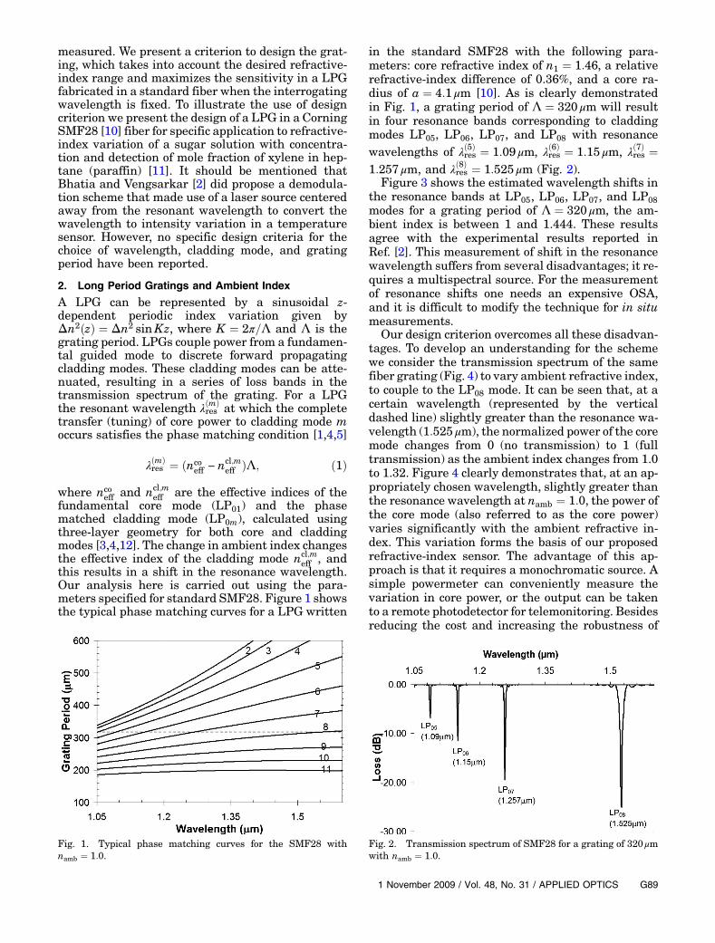
measured. We present a criterion to design the grat-ing, which takes into account the desired refractive-index range and maximizes the sensitivity in a LPGfabricated in a standard fiber when the interrogatingwavelength is fixed. To illustrate the use of designcriterion we present the design of a LPG in a CorningSMF28 [10] fiber for specific application to refractive-index variation of a sugar solution with concentra-tion and detection of mole fraction of xylene in hep-tane (paraffin) [11]. It should be mentioned thatBhatia and Vengsarkar [2] did propose a demodula-tion scheme that made use of a laser source centeredaway from the resonant wavelength to convert thewavelength to intensity variation in a temperaturesensor. However, no specific design criteria for thechoice of wavelength, cladding mode, and gratingperiod have been reported.
2. Long Period Gratings and Ambient Index
A LPG can be represented by a sinusoidal z-dependent periodic index variation given byΔn2ðzÞ ¼ Δn2 sinKz, where K ¼ 2π=Λ and Λ is thegrating period. LPGs couple power from a fundamen-tal guided mode to discrete forward propagatingcladding modes. These cladding modes can be atte-nuated, resulting in a series of loss bands in thetransmission spectrum of the grating. For a LPGthe resonant wavelength λðmÞ
res at which the completetransfer (tuning) of core power to cladding mode moccurs satisfies the phase matching condition [1,4,5]
λðmÞres ¼ ðnco
eff − ncl;meff ÞΛ; ð1Þ
where ncoeff and ncl;m
eff are the effective indices of thefundamental core mode (LP01) and the phasematched cladding mode (LP0m), calculated usingthree-layer geometry for both core and claddingmodes [3,4,12]. The change in ambient index changesthe effective index of the cladding mode ncl;m
eff , andthis results in a shift in the resonance wavelength.Our analysis here is carried out using the para-meters specified for standard SMF28. Figure 1 showsthe typical phase matching curves for a LPG written
in the standard SMF28 with the following para-meters: core refractive index of n1 ¼ 1:46, a relativerefractive-index difference of 0.36%, and a core ra-dius of a ¼ 4:1 μm [10]. As is clearly demonstratedin Fig. 1, a grating period of Λ ¼ 320 μm will resultin four resonance bands corresponding to claddingmodes LP05, LP06, LP07, and LP08 with resonancewavelengths of λð5Þres ¼ 1:09 μm, λð6Þres ¼ 1:15 μm, λð7Þres ¼1:257 μm, and λð8Þres ¼ 1:525 μm (Fig. 2).
Figure 3 shows the estimated wavelength shifts inthe resonance bands at LP05, LP06, LP07, and LP08modes for a grating period of Λ ¼ 320 μm, the am-bient index is between 1 and 1.444. These resultsagree with the experimental results reported inRef. [2]. This measurement of shift in the resonancewavelength suffers from several disadvantages; it re-quires a multispectral source. For the measurementof resonance shifts one needs an expensive OSA,and it is difficult to modify the technique for in situmeasurements.
Our design criterion overcomes all these disadvan-tages. To develop an understanding for the schemewe consider the transmission spectrum of the samefiber grating (Fig. 4) to vary ambient refractive index,to couple to the LP08 mode. It can be seen that, at acertain wavelength (represented by the verticaldashed line) slightly greater than the resonance wa-velength (1:525 μm), the normalized power of the coremode changes from 0 (no transmission) to 1 (fulltransmission) as the ambient index changes from 1.0to 1.32. Figure 4 clearly demonstrates that, at an ap-propriately chosen wavelength, slightly greater thanthe resonance wavelength at namb ¼ 1:0, the power ofthe core mode (also referred to as the core power)varies significantly with the ambient refractive in-dex. This variation forms the basis of our proposedrefractive-index sensor. The advantage of this ap-proach is that it requires a monochromatic source. Asimple powermeter can conveniently measure thevariation in core power, or the output can be takento a remote photodetector for telemonitoring. Besidesreducing the cost and increasing the robustness of
Fig. 1. Typical phase matching curves for the SMF28 withnamb ¼ 1:0.
Fig. 2. Transmission spectrum of SMF28 for a grating of 320 μmwith namb ¼ 1:0.
1 November 2009 / Vol. 48, No. 31 / APPLIED OPTICS G89
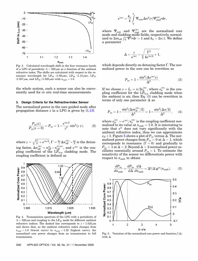
the whole system, such a sensor can also be conve-niently used for in situ real-time measurements.
3. Design Criteria for the Refractive-Index Sensor
The normalized power in the core guided mode afterpropagation distance z in a LPG is given by [1,13]
PcoðzÞPcoðz ¼ 0Þ ¼ Pco ¼ 1 −
κðmÞ2
γ2 sin2ðγ zÞ; ð2Þ
where γ ¼ffiffiffiffiffiffiffiffiffiffiffiffiffiffiffiffiffiffiffiffiΓ2
4 þ κðmÞ2q
, Γ ¼ 2πλ ΔnðmÞ
eff −2πΛ is the detun-
ing factor, ΔnðmÞeff ¼ nco
eff − ncl;ðmÞeff , and κðmÞ is the cou-
pling coefficient of the LP0;m cladding mode. Thecoupling coefficient is defined as
κðmÞ ¼ ko4
Za0
ΨcoreΔn2ðrÞΨðmÞcladrdr;
where Ψcore and ΨðmÞclad are the normalized core
mode and cladding mode fields, respectively, normal-ized to 2πneff
R∞
0 Ψ2rdr ¼ 1 and k0 ¼ 2π=λ. We definea parameter
Δ ¼ γκðmÞ ¼
ffiffiffiffiffiffiffiffiffiffiffiffiffiffiffiffiffiffiffiffiffiffiΓ2
4κðmÞ2 þ 1
s;
which depends directly on detuning factor Γ. The nor-malized power in the core can be rewritten as
Pco ¼ 1 −sin2ðΔκðmÞzÞ
Δ2 : ð3Þ
If we choose z ¼ Lc ¼ π=2κðmÞ0 , where κðmÞ
0 is the cou-pling coefficient for the LP0;m cladding mode whenthe ambient is air, then Eq. (3) can be rewritten interms of only one parameter Δ as
Pco ¼ 1 −sin2ðΔπκðmÞ
N =2ÞΔ2 ¼ 1 −
sin2ðΔπ=2ÞΔ2 ; ð4Þ
where κðmÞN ¼ κðmÞ=κðmÞ
0 is the coupling coefficient nor-malized to its value at namb ¼ 1:0. It is interesting tonote that κm does not vary significantly with theambient refractive index, thus we can approximateκN ≈ 1. Figure 5 shows a plot of Pco versusΔ. The nor-malized power changes from Pco ¼ 0 at Δ ¼ 1, whichcorresponds to resonance ðΓ ¼ 0Þ and gradually toPco ¼ 1 atΔ ¼ 2. BeyondΔ ¼ 2 normalized power os-cillates essentially around Pco ¼ 1. To estimate thesensitivity of the sensor we differentiate power withrespect to namb to obtain
dPco
dnamb¼ dPco
dΔdΔ
dnamb¼ 2f ðΔÞgmðnambÞ; ð5Þ
Fig. 3. Calculated wavelength shift in the four resonance bandsof a LPG of periodicity Λ ¼ 320 μm as a function of the ambientrefractive index. The shifts are calculated with respect to the re-sonance wavelength for LP05 (1:09 μm), LP06 (1:15 μm), LP07
(1:257 μm, and LP08 (1:525 μm) with namb ¼ 1:0.
Fig. 4. Transmission spectrum of the LPG with a periodicity ofΛ ¼ 320 μm and coupling to the LP08 mode for different ambientrefractive indices. The dashed line corresponds to λ ¼ 1:525 μmand shows that, as the ambient refractive index changes fromnamb ¼ 1:0 (lowest curve) to namb ¼ 1:32 (highest curve), thenormalized core power changes from no transmission to fulltransmission.
Fig. 5. Variation of the normalized core power and function f ðΔÞwith Δ.
G90 APPLIED OPTICS / Vol. 48, No. 31 / 1 November 2009
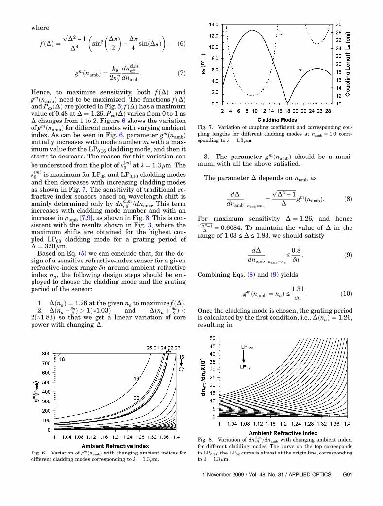
where
f ðΔÞ ¼ffiffiffiffiffiffiffiffiffiffiffiffiffiffiΔ2
− 1p
Δ4
�sin2
�Δπ2
�−Δπ4
sinðΔπÞ�; ð6Þ
gmðnambÞ ¼k02κm0
dncl;meff
dnamb: ð7Þ
Hence, to maximize sensitivity, both f ðΔÞ andgmðnambÞ need to be maximized. The functions f ðΔÞand PcoðΔÞ are plotted in Fig. 5; f ðΔÞ has a maximumvalue of 0.48 atΔ ¼ 1:26; PcoðΔÞ varies from 0 to 1 asΔ changes from 1 to 2. Figure 6 shows the variationof gmðnambÞ for different modes with varying ambientindex. As can be seen in Fig. 6, parameter gmðnambÞinitially increases with mode number m with a max-imum value for the LP0;18 cladding mode, and then itstarts to decrease. The reason for this variation canbe understood from the plot of κðmÞ
0 at λ ¼ 1:3 μm. TheκðmÞ0 is maximum for LP08 and LP0;10 cladding modesand then decreases with increasing cladding modesas shown in Fig. 7. The sensitivity of traditional re-fractive-index sensors based on wavelength shift ismainly determined only by dncl;m
eff =dnamb. This termincreases with cladding mode number and with anincrease in namb [7,9], as shown in Fig. 8. This is con-sistent with the results shown in Fig. 3, where themaximum shifts are obtained for the highest cou-pled LP08 cladding mode for a grating period ofΛ ¼ 320 μm.Based on Eq. (5) we can conclude that, for the de-
sign of a sensitive refractive-index sensor for a givenrefractive-index range δn around ambient refractiveindex na, the following design steps should be em-ployed to choose the cladding mode and the gratingperiod of the sensor:
1. ΔðnaÞ ¼ 1:26 at the given na to maximize f ðΔÞ.2. Δðna −
δn2 Þ > 1ð≈1:03Þ and Δðna þ δn
2 Þ <2ð≈1:83Þ so that we get a linear variation of corepower with changing Δ.
3. The parameter gmðnambÞ should be a maxi-mum, with all the above satisfied.
The parameter Δ depends on namb as
dΔdnamb
����namb¼na
¼ffiffiffiffiffiffiffiffiffiffiffiffiffiffiΔ2
− 1p
Δ gmðnambÞ: ð8Þ
For maximum sensitivity Δ ¼ 1:26, and henceffiffiffiffiffiffiffiffiffiΔ2
−1p
Δ ¼ 0:6084. To maintain the value of Δ in therange of 1:03 ≤ Δ ≤ 1:83, we should satisfy
dΔdnamb
����namb¼na
≤0:8δn : ð9Þ
Combining Eqs. (8) and (9) yields
gmðnamb ¼ naÞ ≤1:31δn : ð10Þ
Once the cladding mode is chosen, the grating periodis calculated by the first condition, i.e., ΔðnaÞ ¼ 1:26,resulting in
Fig. 6. Variation of gmðnambÞ with changing ambient indices fordifferent cladding modes corresponding to λ ¼ 1:3 μm.
Fig. 7. Variation of coupling coefficient and corresponding cou-pling lengths for different cladding modes at namb ¼ 1:0 corre-sponding to λ ¼ 1:3 μm.
Fig. 8. Variation of dncl;meff =dnamb with changing ambient index,
for different cladding modes. The curve on the top correspondsto LP0;25; the LP02 curve is almost at the origin line, correspondingto λ ¼ 1:3 μm.
1 November 2009 / Vol. 48, No. 31 / APPLIED OPTICS G91
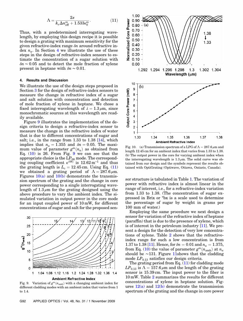
Λ ¼ 2πkoΔnm
eff þ 1:533κm0: ð11Þ
Thus, with a predetermined interrogating wave-length, by employing this design recipe it is possibleto design a grating with maximum sensitivity for thegiven refractive-index range δn around refractive in-dex na. In Section 4 we illustrate the use of thesesteps in the design of refractive-index sensors to es-timate the concentration of a sugar solution withδn∼ 0:05 and to detect the mole fraction of xylenepresent in heptane with δn∼ 0:01.
4. Results and Discussion
We illustrate the use of the design steps proposed inSection 3 for the design of refractive-index sensors tomeasure the change in refractive index of a sugarand salt solution with concentration and detectionof mole fraction of xylene in heptane. We chose afixed interrogating wavelength of λ ¼ 1:3 μm, sincemonochromatic sources at this wavelength are read-ily available.Figure 9 illustrates the implementation of the de-
sign criteria to design a refractive-index sensor tomeasure the change in the refractive index of waterthat is due to different concentrations of sugar andsalt; i.e., in the range from 1.33 to 1.38 [14], whichimplies that na ¼ 1:355 and δn ¼ 0:05. The maxi-mum value of parameter gmðnaÞ as obtained fromEq. (10) is 26. From Fig. 9 we can see that theappropriate choice is the LP08 mode. The correspond-ing coupling coefficient κð08Þ is 12:62m−1 and thusthe grating length is Lc ¼ 12:45 cm. Using Eq. (11)we obtained a grating period of Λ ¼ 287:6 μm.Figures 10(a) and 10(b) demonstrate the transmis-sion spectrum of the grating and the change in corepower corresponding to a single interrogating wave-length of 1:3 μm for the grating designed using theabove procedure to vary the ambient index. The si-mulated variation in output power in the core modefor an input coupled power of 10mW, for differentconcentrations of sugar and salt for the proposed sen-
sor structure is tabulated in Table 1. The variation ofpower with refractive index is almost linear in therange of interest, i.e., for a refractive-index variationfrom 1.33 to 1.38. (The concentration of sugar ex-pressed in Brix or °bx is a scale used to determinethe percentage of sugar by weight in grams per100 mm of water.)
Employing the same procedure we next design asensor for variation of the refractive index of heptane(paraffin) that is due to the presence of xylene, whichis of interest in the petroleum industry [11]. We pre-sent a design for the detection of very low concentra-tions of xylene. Table 2 shows that the refractive-index range for such a low concentration is from1.37 to 1.38 [11]. Hence, for δn ¼ 0:01 and na ¼ 1:375,from Eq. (10) the value of parameter gmðnambÞ at nashould be ∼131. Figure 11shows that the claddingmode LP0;13 satisfies our design criteria.
The grating period from Eq. (11) for cladding modeLP0;13 is Λ ¼ 157:6 μm and the length of the gratingsensor is 15:39 cm. The input power to the fiber is10mW. Table 2 summarizes the results for differentconcentrations of xylene in heptane solution. Fig-ures 12(a) and 12(b) demonstrate the transmissionspectrum of the grating and the change in core power
Fig. 9. Variation of gmðnambÞ with a changing ambient index fordifferent cladding modes with an ambient index that varies from 1to 1.4.
Fig. 10. (a) Transmission spectrum of a LPG ofΛ ¼ 287:6 μm andlength 12:45 cm for an ambient index that varies from 1.33 to 1.38.(b) The output power in the core for varying ambient index whenthe interrogating wavelength is 1:3 μm. The solid curve was ob-tained from our design and the symbols represent the results ob-tained with OptiGrating (Optiwave, Ottawa, Ontario, Canada).
G92 APPLIED OPTICS / Vol. 48, No. 31 / 1 November 2009
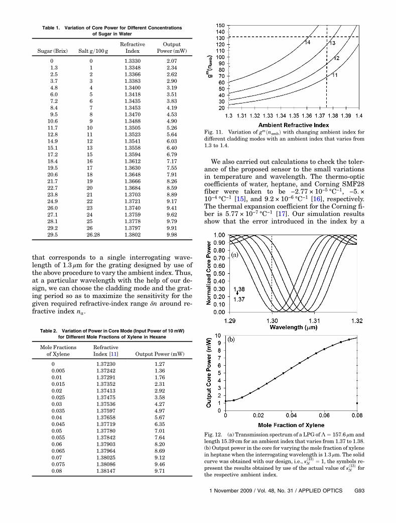
that corresponds to a single interrogating wave-length of 1:3 μm for the grating designed by use ofthe above procedure to vary the ambient index. Thus,at a particular wavelength with the help of our de-sign, we can choose the cladding mode and the grat-ing period so as to maximize the sensitivity for thegiven required refractive-index range δn around re-fractive index na.
We also carried out calculations to check the toler-ance of the proposed sensor to the small variationsin temperature and wavelength. The thermo-opticcoefficients of water, heptane, and Corning SMF28fiber were taken to be −2:77 × 10−5 °C−1, −5: ×10−4 °C−1 [15], and 9:2 × 10⁻⁶ °C−1 [16], respectively.The thermal expansion coefficient for the Corning fi-ber is 5:77 × 10−7 °C−1 [17]. Our simulation resultsshow that the error introduced in the index by a
Table 1. Variation of Core Power for Different Concentrationsof Sugar in Water
Sugar (Brix) Salt g=100gRefractive
IndexOutput
Power (mW)
0 0 1.3330 2.071.3 1 1.3348 2.342.5 2 1.3366 2.623.7 3 1.3383 2.904.8 4 1.3400 3.196.0 5 1.3418 3.517.2 6 1.3435 3.838.4 7 1.3453 4.199.5 8 1.3470 4.53
10.6 9 1.3488 4.9011.7 10 1.3505 5.2612.8 11 1.3523 5.6414.9 12 1.3541 6.0315.1 13 1.3558 6.4017.2 15 1.3594 6.7918.4 16 1.3612 7.1719.5 17 1.3630 7.5520.6 18 1.3648 7.9121.7 19 1.3666 8.2622.7 20 1.3684 8.5923.8 21 1.3703 8.8924.9 22 1.3721 9.1726.0 23 1.3740 9.4127.1 24 1.3759 9.6228.1 25 1.3778 9.7929.2 26 1.3797 9.9129.5 26.28 1.3802 9.98
Table 2. Variation of Power in Core Mode (Input Power of 10 mW)for Different Mole Fractions of Xylene in Hexane
Mole Fractionsof Xylene
RefractiveIndex [11] Output Power (mW)
0 1.37230 1.270.005 1.37242 1.360.01 1.37291 1.760.015 1.37352 2.310.02 1.37413 2.920.025 1.37475 3.580.03 1.37536 4.270.035 1.37597 4.970.04 1.37658 5.670.045 1.37719 6.350.05 1.37780 7.010.055 1.37842 7.640.06 1.37903 8.200.065 1.37964 8.690.07 1.38025 9.120.075 1.38086 9.460.08 1.38147 9.71
Fig. 11. Variation of gmðnambÞ with changing ambient index fordifferent cladding modes with an ambient index that varies from1.3 to 1.4.
Fig. 12. (a) Transmission spectrum of a LPG ofΛ ¼ 157:6 μm andlength 15:39 cm for an ambient index that varies from 1.37 to 1.38.(b) Output power in the core for varying the mole fraction of xylenein heptane when the interrogating wavelength is 1:3 μm. The solidcurve was obtained with our design, i.e., κð13ÞN ¼ 1, the symbols re-present the results obtained by use of the actual value of κð13ÞN forthe respective ambient index.
1 November 2009 / Vol. 48, No. 31 / APPLIED OPTICS G93
0:1 °C increase in temperature is 0.00007 at 1.3558for the sensor designed for a sugar and salt solution.The error introduced in the detection of the molefraction of xylene in heptane is less than 0.0004.Our simulation results also show that a wavelengthshift of �0:008nm introduces an index error of lessthan �0:0002 for both sensors. Commercially avail-able refractometers (both inline and laboratory use)specify resolution in the range from ≈10−4 to ≈10−6
and an error in refractive index from �0:0002 to�0:00004. In comparison with these refractometers,our proposed design offers a resolution of ≈10−5 whenthe resolution of the detector is −20 dBm, which canbe improved further by increasing the resolution ofthe detector system. The error in refractive indexis less than �0:0004, which can also be improvedby increasing the resolution of the detector system.Thus our proposed design satisfies the existing stan-dards and offers the possibility to improve the stan-dards with only a slight increase in cost.
5. Conclusions
We have presented a detailed analysis for a LPGrefractive-index sensor based on the detection ofchange in core power. A design was developed tomake possible cladding modes and grating periodswith maximum sensitivity. The sensor can be usedfor the quality assurance of different fluids such aswater, milk, and kerosene. The LPG sensor has beendemonstrated to measure changes in refractive indexas low as (≈10−5), which offers an attractive alterna-tive to the existing high performance liquid chroma-tography andUV spectroscopy approaches used in oilrefineries without any loss of accuracy. The majoradvantage of such a LPG sensor is that it is robust,inexpensive, compact, and can be used for in situmeasurements.
References1. A. M. Vengaskar, P. J. Lemaire, J. B. Judkins, V. Bhatia,
T. Erdogan, and J. E. Sipe, “Long period fiber gratings as bandrejection filters,” J. Lightwave Technol. 14, 58–64 (1996).
2. V. Bhatia and A. M. Vengsarkar, “Optical fiber long-periodgrating sensors,” Opt. Lett. 21, 692–694 (1996).
3. R. Singh, H. Kumar, and E. K. Sharma, “Design of long periodgratings necessity of a three layer fiber geometry for claddingmode characteristics,” Microwave Opt. Technol. Lett. 37,45–49 (2003).
4. T. Erdogan, “Cladding mode resonances in short- and long-period fiber grating filters,” J. Opt. Soc. Am. A 14, 1760–1773(1997).
5. T. Erdogan, “Fiber grating spectra,” J. Lightwave Technol. 15,1277–1294 (1997).
6. T. Zhu, Y-J. Rao, and Q-J. Mo, “Simultaneous measurementof refractive index and temperature using a single ultra-long-period fiber grating,” IEEE Photon. Technol. Lett. 17,2700–2702 (2005).
7. V. Bhatia, “Applications of long-period gratings to singleand multi-parameter sensing,” Opt. Express 4, 457–466(1999).
8. H. J. Patrick, A. D. Kersey, and F. Bucholtz, “Analysis ofthe response of long period fiber gratings to externalindex of refraction,” J. Lightwave Technol. 16 1606–1612(1998).
9. X. Shu, L. Zhang, and I. Bennion, “Sensitivity characteristicsof long period fiber gratings,” J. Lightwave Technol. 20,255–266 (2002).
10. Corning Incorporated, “Corning SMF28e optical fiber productinformation,” http://www.corning.com/assets/0/433/573/583/09573389‑147D‑4CBC‑B55F‑18C817D5F800.pdf.
11. M. Domínguez-Perez, L. Segade , O. Cabeza, C. Franjo, andE. Jiménez, “Densities, surface tensions, and refractive in-dices of propyl propanoate+hexane+m-xylene at 298:15K,”J. Chem. Eng. Data 51, 294–300 (2006).
12. M. Monerie, “Propagation in doubly clad single mode fibers,”IEEE J. Quantum Electron. 18, 533–542 (2003).
13. A. Ghatak and K. Thyagrajan, Introduction to Fiber Optics(Cambridge U. Press, 1998), pp. 543–546.
14. Topac, Incorporated, “Relationship between salt solution andsugar concentration (Brix) and refractive index at 20 °C,”www.topac.com/salinity_brix.html.
15. R. C. Weast, ed., Handbook of Physics and Chemistry (CRCPress, 1982).
16. S. Chang, C-C. Hsu, T-H. Huang, W-C. Chuang, Y-S. Tsai,J-Y. Shieh, and C-Y. Leung, “Heterodyne interferometric mea-surement of the thermo-optic coefficient of single mode fiber,”Chin. J. Phys. 38, 437–442 (2000).
17. M. Bousonville and J. Rausch, “Velocity of signal delaychanges in fiber optic cables,” in Proceedings of the Ninth Eur-opean Workshop on Beam Diagnostics and Instrumentationfor Particle Accelerators (DIPAC)( 2009).
G94 APPLIED OPTICS / Vol. 48, No. 31 / 1 November 2009

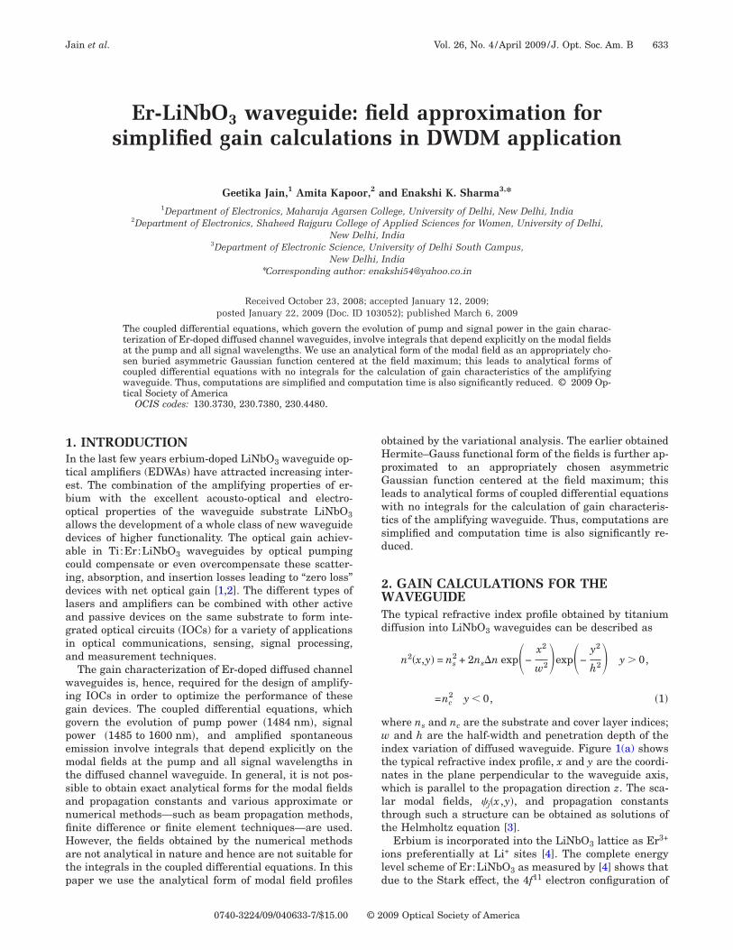
1Iteboadacidlagia
wiggpemtsanfiHatp
Jain et al. Vol. 26, No. 4 /April 2009 /J. Opt. Soc. Am. B 633
Er-LiNbO3 waveguide: field approximation forsimplified gain calculations in DWDM application
Geetika Jain,1 Amita Kapoor,2 and Enakshi K. Sharma3,*1Department of Electronics, Maharaja Agarsen College, University of Delhi, New Delhi, India
2Department of Electronics, Shaheed Rajguru College of Applied Sciences for Women, University of Delhi,New Delhi, India
3Department of Electronic Science, University of Delhi South Campus,New Delhi, India
*Corresponding author: [email protected]
Received October 23, 2008; accepted January 12, 2009;posted January 22, 2009 (Doc. ID 103052); published March 6, 2009
The coupled differential equations, which govern the evolution of pump and signal power in the gain charac-terization of Er-doped diffused channel waveguides, involve integrals that depend explicitly on the modal fieldsat the pump and all signal wavelengths. We use an analytical form of the modal field as an appropriately cho-sen buried asymmetric Gaussian function centered at the field maximum; this leads to analytical forms ofcoupled differential equations with no integrals for the calculation of gain characteristics of the amplifyingwaveguide. Thus, computations are simplified and computation time is also significantly reduced. © 2009 Op-tical Society of America
OCIS codes: 130.3730, 230.7380, 230.4480.
oHpGlwtsd
2WTd
wwitnwltt
ild
. INTRODUCTIONn the last few years erbium-doped LiNbO3 waveguide op-ical amplifiers (EDWAs) have attracted increasing inter-st. The combination of the amplifying properties of er-ium with the excellent acousto-optical and electro-ptical properties of the waveguide substrate LiNbO3llows the development of a whole class of new waveguideevices of higher functionality. The optical gain achiev-ble in Ti:Er:LiNbO3 waveguides by optical pumpingould compensate or even overcompensate these scatter-ng, absorption, and insertion losses leading to “zero loss”evices with net optical gain [1,2]. The different types ofasers and amplifiers can be combined with other activend passive devices on the same substrate to form inte-rated optical circuits (IOCs) for a variety of applicationsn optical communications, sensing, signal processing,nd measurement techniques.The gain characterization of Er-doped diffused channel
aveguides is, hence, required for the design of amplify-ng IOCs in order to optimize the performance of theseain devices. The coupled differential equations, whichovern the evolution of pump power �1484 nm�, signalower �1485 to 1600 nm�, and amplified spontaneousmission involve integrals that depend explicitly on theodal fields at the pump and all signal wavelengths in
he diffused channel waveguide. In general, it is not pos-ible to obtain exact analytical forms for the modal fieldsnd propagation constants and various approximate orumerical methods—such as beam propagation methods,nite difference or finite element techniques—are used.owever, the fields obtained by the numerical methodsre not analytical in nature and hence are not suitable forhe integrals in the coupled differential equations. In thisaper we use the analytical form of modal field profiles
0740-3224/09/040633-7/$15.00 © 2
btained by the variational analysis. The earlier obtainedermite–Gauss functional form of the fields is further ap-roximated to an appropriately chosen asymmetricaussian function centered at the field maximum; this
eads to analytical forms of coupled differential equationsith no integrals for the calculation of gain characteris-
ics of the amplifying waveguide. Thus, computations areimplified and computation time is also significantly re-uced.
. GAIN CALCULATIONS FOR THEAVEGUIDE
he typical refractive index profile obtained by titaniumiffusion into LiNbO3 waveguides can be described as
n2�x,y� = ns2 + 2ns�n exp�−
x2
w2�exp�−y2
h2� y � 0,
=nc2 y � 0, �1�
here ns and nc are the substrate and cover layer indices;and h are the half-width and penetration depth of the
ndex variation of diffused waveguide. Figure 1(a) showshe typical refractive index profile, x and y are the coordi-ates in the plane perpendicular to the waveguide axis,hich is parallel to the propagation direction z. The sca-
ar modal fields, �j�x ,y�, and propagation constantshrough such a structure can be obtained as solutions ofhe Helmholtz equation [3].
Erbium is incorporated into the LiNbO3 lattice as Er3+
ons preferentially at Li+ sites [4]. The complete energyevel scheme of Er:LiNbO3 as measured by [4] shows thatue to the Stark effect, the 4f11 electron configuration of
009 Optical Society of America
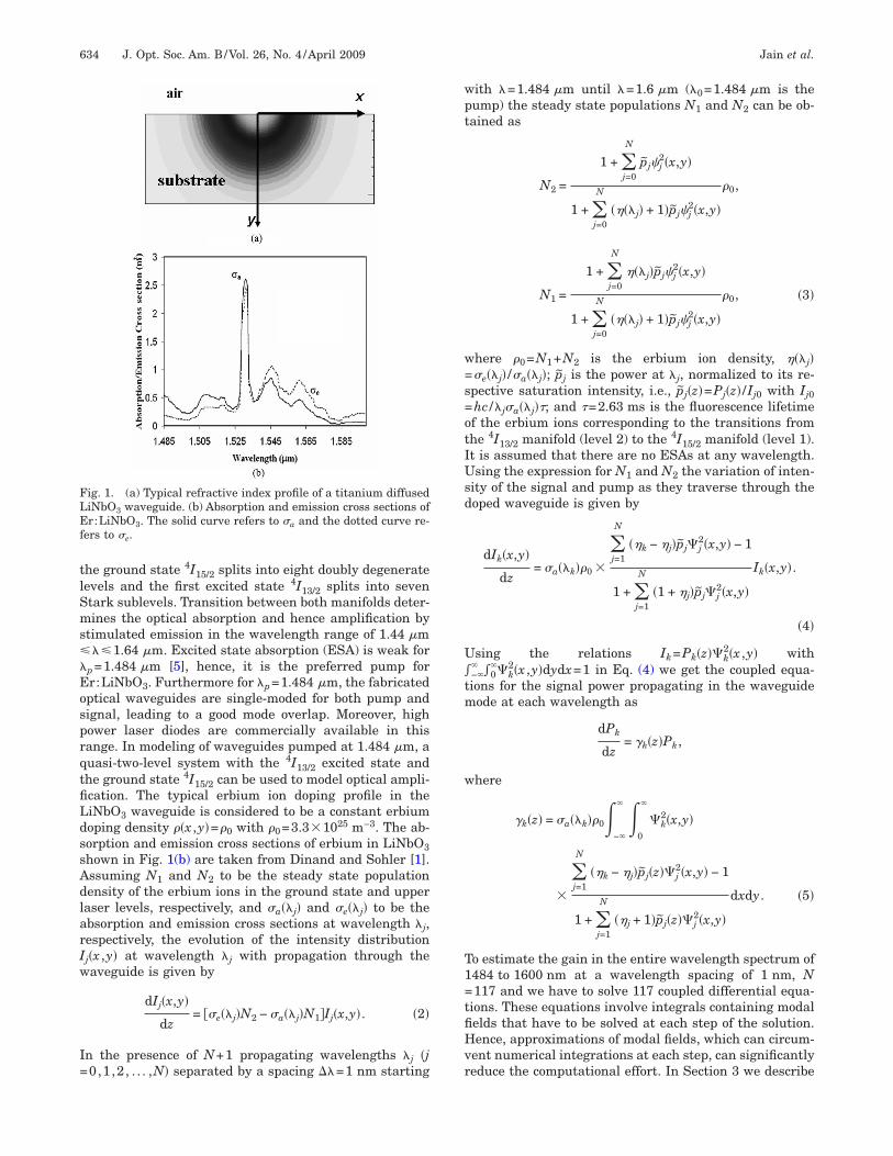
tlSms��EosprqtfiLdssAdlarIw
I=
wpt
w=s=otIUsd
U�tm
w
T1=tfiHvr
FLEf
634 J. Opt. Soc. Am. B/Vol. 26, No. 4 /April 2009 Jain et al.
he ground state 4I15/2 splits into eight doubly degenerateevels and the first excited state 4I13/2 splits into seventark sublevels. Transition between both manifolds deter-ines the optical absorption and hence amplification by
timulated emission in the wavelength range of 1.44 �m��1.64 �m. Excited state absorption (ESA) is weak for
p=1.484 �m [5], hence, it is the preferred pump forr:LiNbO3. Furthermore for �p=1.484 �m, the fabricatedptical waveguides are single-moded for both pump andignal, leading to a good mode overlap. Moreover, highower laser diodes are commercially available in thisange. In modeling of waveguides pumped at 1.484 �m, auasi-two-level system with the 4I13/2 excited state andhe ground state 4I15/2 can be used to model optical ampli-cation. The typical erbium ion doping profile in theiNbO3 waveguide is considered to be a constant erbiumoping density ��x ,y�=�0 with �0=3.31025 m−3. The ab-orption and emission cross sections of erbium in LiNbO3hown in Fig. 1(b) are taken from Dinand and Sohler [1].ssuming N1 and N2 to be the steady state populationensity of the erbium ions in the ground state and upperaser levels, respectively, and a��j� and e��j� to be thebsorption and emission cross sections at wavelength �j,espectively, the evolution of the intensity distributionj�x ,y� at wavelength �j with propagation through theaveguide is given by
dIj�x,y�
dz= �e��j�N2 − a��j�N1�Ij�x,y�. �2�
n the presence of N+1 propagating wavelengths �j �j0,1,2, . . . ,N� separated by a spacing ��=1 nm starting
ig. 1. (a) Typical refractive index profile of a titanium diffusediNbO3 waveguide. (b) Absorption and emission cross sections ofr:LiNbO3. The solid curve refers to a and the dotted curve re-
ers to e.
ith �=1.484 �m until �=1.6 �m (�0=1.484 �m is theump) the steady state populations N1 and N2 can be ob-ained as
N2 =
1 + �j=0
N
p̃j�j2�x,y�
1 + �j=0
N
����j� + 1�p̃j�j2�x,y�
�0,
N1 =
1 + �j=0
N
���j�p̃j�j2�x,y�
1 + �j=0
N
����j� + 1�p̃j�j2�x,y�
�0, �3�
here �0=N1+N2 is the erbium ion density, ���j�e��j� /a��j�; p̃j is the power at �j, normalized to its re-pective saturation intensity, i.e., p̃j�z�=Pj�z� /Ij0 with Ij0hc /�ja��j��; and �=2.63 ms is the fluorescence lifetimef the erbium ions corresponding to the transitions fromhe 4I13/2 manifold (level 2) to the 4I15/2 manifold (level 1).t is assumed that there are no ESAs at any wavelength.sing the expression for N1 and N2 the variation of inten-
ity of the signal and pump as they traverse through theoped waveguide is given by
dIk�x,y�
dz= a��k��0
�j=1
N
��k − �j�p̃j j2�x,y� − 1
1 + �j=1
N
�1 + �j�p̃j j2�x,y�
Ik�x,y�.
�4�
sing the relations Ik=Pk�z� k2�x ,y� with
−�� �0
� k2�x ,y�dydx=1 in Eq. (4) we get the coupled equa-
ions for the signal power propagating in the waveguideode at each wavelength as
dPk
dz= �k�z�Pk,
here
�k�z� = a��k��0−�
� 0
�
k2�x,y�
�j=1
N
��k − �j�p̃j�z� j2�x,y� − 1
1 + �j=1
N
��j + 1�p̃j�z� j2�x,y�
dxdy. �5�
o estimate the gain in the entire wavelength spectrum of484 to 1600 nm at a wavelength spacing of 1 nm, N117 and we have to solve 117 coupled differential equa-
ions. These equations involve integrals containing modalelds that have to be solved at each step of the solution.ence, approximations of modal fields, which can circum-
ent numerical integrations at each step, can significantlyeduce the computational effort. In Section 3 we describe
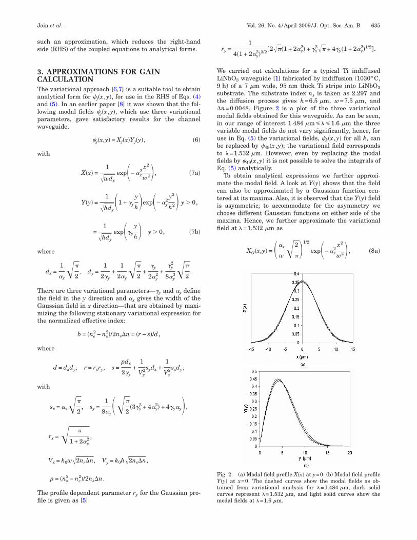
ss
3CTaalpw
w
w
TtGmt
w
w
Tfi
WL9st�mivubtfiE
mcticmfi
FYtcm
Jain et al. Vol. 26, No. 4 /April 2009 /J. Opt. Soc. Am. B 635
uch an approximation, which reduces the right-handide (RHS) of the coupled equations to analytical forms.
. APPROXIMATIONS FOR GAINALCULATIONhe variational approach [6,7] is a suitable tool to obtainnalytical form for �j�x ,y�, for use in the RHS of Eqs. (4)nd (5). In an earlier paper [8] it was shown that the fol-owing modal fields �j�x ,y�, which use three variationalarameters, gave satisfactory results for the channelaveguide,
�j�x,y� = Xj�x�Yj�y�, �6�
ith
X�x� =1
wdx
exp�− �x2
x2
w2� , �7a�
Y�y� =1
hdy�1 + �y
y
h�exp�− �y2y2
h2� y � 0,
=1
hdy
exp��y
y
h� y � 0, �7b�
here
dx =1
�x�
2, dy =
1
2�y+
1
2�y�
2+
�y
2�y2 +
�y2
8�y3�
2.
here are three variational parameters—�y and �y definehe field in the y direction and �x gives the width of theaussian field in x direction—that are obtained by maxi-izing the following stationary variational expression for
he normalized effective index:
b = �ne2 − ns
2�/2ns�n = �r − s�/d,
here
d = dxdy, r = rxry, s =pdx
2�y+
1
Vy2sydx +
1
Vx2sxdy,
ith
sx = �x�
2, sy =
1
8�y��
2�3�y
2 + 4�y2� + 4�y�y� ,
rx = �
1 + 2�x2 ,
Vx = k0w2ns�n, Vy = k0h2ns�n,
p = �ns2 − nc
2�/2ns�n.
he profile dependent parameter ry for the Gaussian pro-le is given as [5]
ry =1
4�1 + 2�y2�3/2
�2��1 + 2�y2� + �y
2� + 4�y�1 + 2�y2�1/2�.
e carried out calculations for a typical Ti indiffusediNbO3 waveguide [1] fabricated by indiffusion (1030°C,h) of a 7 �m wide, 95 nm thick Ti stripe into LiNbO3
ubstrate. The substrate index ns is taken as 2.297 andhe diffusion process gives h=6.5 �m, w=7.5 �m, andn=0.0048. Figure 2 is a plot of the three variationalodal fields obtained for this waveguide. As can be seen,
n our range of interest 1.484 �m���1.6 �m the threeariable modal fields do not vary significantly, hence, forse in Eq. (5) the variational fields, �k�x ,y� for all k, cane replaced by �49�x ,y�; the variational field correspondso �=1.532 �m. However, even by replacing the modalelds by �49�x ,y� it is not possible to solve the integrals ofq. (5) analytically.To obtain analytical expressions we further approxi-ate the modal field. A look at Y�y� shows that the field
an also be approximated by a Gaussian function cen-ered at its maxima. Also, it is observed that the Y�y� fields asymmetric; to accommodate for the asymmetry wehoose different Gaussian functions on either side of theaxima. Hence, we further approximate the variationaleld at �=1.532 �m as
XG�x,y� = ��x
w2
��1/2
exp�− �x2
x2
w2� , �8a�
ig. 2. (a) Modal field profile X�x� at y=0. (b) Modal field profile�y� at x=0. The dashed curves show the modal fields as ob-
ained from variational analysis for �=1.484 �m, dark solidurves represent �=1.532 �m, and light solid curves show theodal fields at �=1.6 �m.
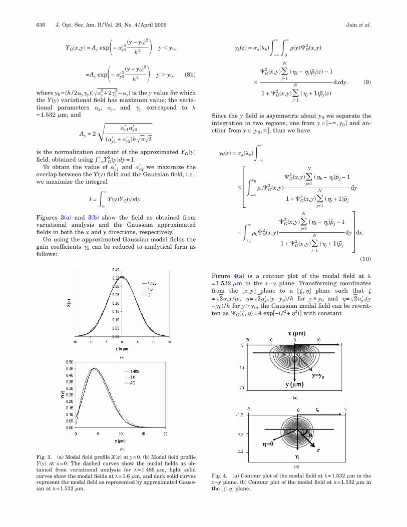
wtt=
ifi
ow
Fvfi
gf
Sio
F=f=−t
FYtcri
Fxt
636 J. Opt. Soc. Am. B/Vol. 26, No. 4 /April 2009 Jain et al.
YG�x,y� = Ay exp�− �y1�2�y − y0�2
h2 � y � y0,
=Ay exp�− �y2�2�y − y0�2
h2 � y � y0, �8b�
here y0= �h /2�y�y���y2+2�y
2−�y� is the y value for whichhe Y�y� variational field has maximum value; the varia-ional parameters �x, �y, and �y correspond to �1.532 �m; and
Ay = 2 �y1� �y2�
��y1� + �y2� �h�2
s the normalization constant of the approximated YG�y�eld, obtained using �−�
� YG2 �y�dy=1.
To obtain the value of �y1� and �y2� we maximize theverlap between the Y�y� field and the Gaussian field, i.e.,e maximize the integral
I =0
�
Y�y�YG�y�dy.
igures 3(a) and 3(b) show the field as obtained fromariational analysis and the Gaussian approximatedelds in both the x and y directions, respectively.On using the approximated Gaussian modal fields the
ain coefficients �k can be reduced to analytical form asollows:
ig. 3. (a) Modal field profile X�x� at y=0. (b) Modal field profile�y� at x=0. The dashed curves show the modal fields as ob-
ained from variational analysis for �=1.485 �m, light solidurves show the modal fields at �=1.6 �m, and dark solid curvesepresent the modal field as represented by approximated Gauss-an at �=1.532 �m.
�k�z� = a��k�−�
� 0
�
��y� G2 �x,y�
G2 �x,y��
j=1
N
��k − �j�p̃j�z� − 1
1 + G2 �x,y��
j=1
N
��j + 1�p̃j�z�
dxdy. �9�
ince the y field is asymmetric about y0 we separate thentegration in two regions, one from y� �−� ,y0� and an-ther from y� �y0 ,��, thus we have
�k�z� = a��k�−�
�
�−�
y0
�0 G2 �x,y�
G2 �x,y��
j=1
N
��k − �j�p̃j − 1
1 + G2 �x,y��
j=1
N
��j + 1�p̃j
dy
+y0
�
�0 G2 �x,y�
G2 �x,y��
j=1
N
��k − �j�p̃j − 1
1 + G2 �x,y��
j=1
N
��j + 1�p̃j
dy�dx.
�10�
igure 4(a) is a contour plot of the modal field at �1.532 �m in the x–y plane. Transforming coordinates
rom the �x ,y� plane to a �� ,�� plane such that �2�xx /w, �=2�y1� �y−y0� /h for y�y0 and �=2�y2� �yy0� /h for y�y0, the Gaussian modal field can be rewrit-
en as G�� ,��=A exp�−��2+�2�� with constant
ig. 4. (a) Contour plot of the modal field at �=1.532 �m in the–y plane. (b) Contour plot of the modal field at �=1.532 �m inhe �� ,�� plane.
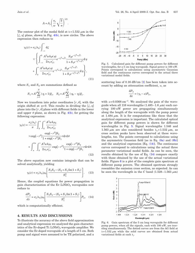
T�e
w
Nopaf
Ts
Hgr
w
4Taicp
sc
wgraaagw1cltacprwfidrb
FwPfiv
Fpe�v
Jain et al. Vol. 26, No. 4 /April 2009 /J. Opt. Soc. Am. B 637
A = Ay��x
w2
��1/2
.
he contour plot of the modal field at �=1.532 �m in the� ,�� plane, shown in Fig. 4(b), is now circles. The abovexpression then reduces to
�k�z� = a��k�−�
�
d�
−�
0 A2wh����
2�x�y1�e−��2+�2�
S2e−��2+�2�
1 + S1e−��2+�2�d�
+0
� A2wh����
2�x�y2�e−��2+�2�
S2e−��2+�2�
1 + S1e−��2+�2�d�� ,
�11�
here S1 and S2 are summations defined as
S1 = A2�j=1
N
��j + 1�p̃j, S2 = A2�j=1
N
��k − �j�p̃j.
ow we transform into polar coordinates �r ,��, with therigin shifted at �=0. This results in dividing the �� ,��lane into the �r ,�� plane with different fields in the lowernd upper � plane, as shown in Fig. 4(b), for getting theollowing expression:
�k�z� =a��k�
�
0
�0
� A2wh�2
2�x�y2�
exp�− r2�exp�− r2�S2
1 + exp�− r2�S1rdrd�
+�
2�0
� A2wh�1
2�x�y1�exp�− r2�
exp�− r2�S2
1 + exp�− r2�S1rdrd�.
�12�
he above equation now contains integrals that can beolved analytically, yielding
�k�z� = a��k��0�S1S2 − �S2 + S1�ln�1 + S1�
S12 � . �13�
ence, the coupled equations for power propagation inain characterization of the Er:LiNbO3 waveguides noweduce to
dPk
dz= a��k��0�S1S2 − �S2 + S1�ln�1 + S1�
S12 �Pk, �14�
hich is computationally efficient.
. RESULTS AND DISCUSSIONSo illustrate the accuracy of the above field approximationnd analytical expression we analyzed the gain character-stics of the Er-doped Ti:LiNbO3 waveguide amplifier. Weonsider the Er-doped waveguide of a length of 5 cm. Bothump and signal were assumed to be TE polarized, and a
cattering loss of 0.16 dB/cm [1] has been taken into ac-ount by adding an attenuation coefficient, �, as
dPk
dz= ��k − ��Pk,
ith �=0.0368 cm−1. We analyzed the gain of the wave-uide when all 116 wavelengths �1.485–1.6 �m� each car-ying 100 nW power are propagating simultaneouslylong the length of the waveguide with the pump powert 1.484 �m. It is for computations like these that thenalytical expression is important. The calculated opticalain for different pump powers is shown for differentavelengths in Fig. 5. Signal wavelengths 1.546 and.563 �m are also considered besides �s=1.532 �m, asross section peaks have been observed at these wave-engths, too. The points correspond to calculations usinghe asymmetric Gaussian field [as in Eq. (8a) and (8b)]nd the analytical expression [Eq. (14)]. The continuousurves correspond to calculations using the actual threearameter variational modal fields. As can be seen, theesults obtained by the use of Eq. (14) compare exactlyith those obtained by the use of the actual variationalelds. Figure 6 is a plot of the complete gain spectrum atifferent pump powers. The obtained spectrum stronglyesembles the emission cross section, as expected. As cane seen the wavelength in the C band �1.528–1.563 �m�
ig. 5. Calculated gain for different pump powers for differentavelengths, for a 5 cm long waveguide. Signal power is 100 nW.oints correspond to calculations using asymmetric Gaussianeld and the continuous curves correspond to the actual threeariational modal fields.
ig. 6. Gain spectrum of the 5 cm long waveguide for differentump powers, when all the signals, each with 100 nW, are trav-ling simultaneously. The dotted curves are from the AG field at=1.532 �m while the solid curves are obtained from actualariational fields at each � .
j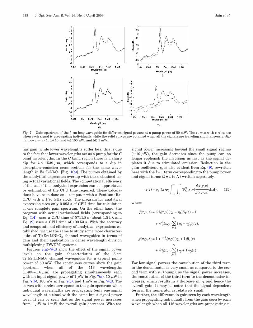
htbdaltiobtCeopEEatigm
lTps�wFciwlf
s�lpgha
w
Fiotcot
ww
Fwn
638 J. Opt. Soc. Am. B/Vol. 26, No. 4 /April 2009 Jain et al.
as gain, while lower wavelengths suffer loss; this is dueo the fact that lower wavelengths act as a pump for the Cand wavelengths. In the C band region there is a sharpip for ��1.539 �m, which corresponds to a dip inbsorption–emission cross sections for the same wave-ength in Er:LiNbO3 [Fig. 1(b)]. The curves obtained byhe analytical expression overlap with those obtained us-ng actual variational fields. The computational efficiencyf the use of the analytical expression can be appreciatedy estimation of the CPU time required. These calcula-ions have been done on a computer with a Pentium (R)4PU with a 1.70 GHz clock. The program for analyticalxpression uses only 0.093 s of CPU time for calculationf one complete gain spectrum. On the other hand, therogram with actual variational fields [corresponding toq. (14)] uses a CPU time of 5711.8 s (about 1.5 h), andq. (9) uses a CPU time of 100.53 s. With the accuracynd computational efficiency of analytical expressions es-ablished, we use the same to study some more character-stics of Ti:Er:LiNbO3 channel waveguides in terms ofain and their application in dense wavelength divisionultiplexing (DWDM) systems.Figures 7(a)–7(d) show the effect of the signal power
evels on the gain characteristics of the 5 cmi:Er:LiNbO3 channel waveguides for a typical pumpower of 50 mW. The continuous curves show the gainpectrum when all of the 116 wavelengths1.485–1.6 �m� are propagating simultaneously eachith an input signal power of 1 �W in Fig. 7(a), 10 �W inig. 7(b), 100 �W in Fig. 7(c), and 1 mW in Fig. 7(d). Theurves with circles correspond to the gain spectrum whenndividual wavelengths are propagating (only one signalavelength at a time) with the same input signal power
evel. It can be seen that as the signal power increasesrom 1 �W to 1 mW the overall gain decreases. With the
ig. 7. Gain spectrum of the 5 cm long waveguide for differenthen each signal is propagating individually while the solid curval power= �a� 1, (b) 10, and (c) 100 �W, and (d) 1 mW.
ignal power increasing beyond the small signal regime�10 �W�, the gain decreases since the pump can noonger replenish the inversion as fast as the signal de-letes it due to stimulated emission. Reduction in theain coefficient �k is also evident from Eq. (9), rewrittenere with the k=1 term corresponding to the pump powernd signal terms (k=2 to N) written separately.
�k�z� = a��k��0−�
� 0
�
G2 �x,y�
f�x,y,z�
g�x,y,z�dxdy, �15�
here
f�x,y,z� = G2 �x,y���k − �1�p̃1�z� − 1
+ G2 �x,y��
j=2
N
��k − �j�p̃j�z�,
g�x,y,z� = 1 + G2 �x,y���1 + 1�p̃1�z�
+ G2 �x,y��
j=2
N
��j + 1�p̃j�z�.
or low signal powers the contribution of the third termn the denominator is very small as compared to the sec-nd term with p̃1 (pump); as the signal power increases,he contribution of the third term to the denominator in-reases, which results in a decrease in �k and hence theverall gain. It may be noted that the signal dependenterm in the numerator is relatively small.
Further, the difference in gain seen by each wavelengthhen propagating individually from the gain seen by eachavelength when all 116 wavelengths are propagating si-
powers at a pump power of 50 mW. The curves with circles areobtained when all the signals are traveling simultaneously. Sig-
signales are
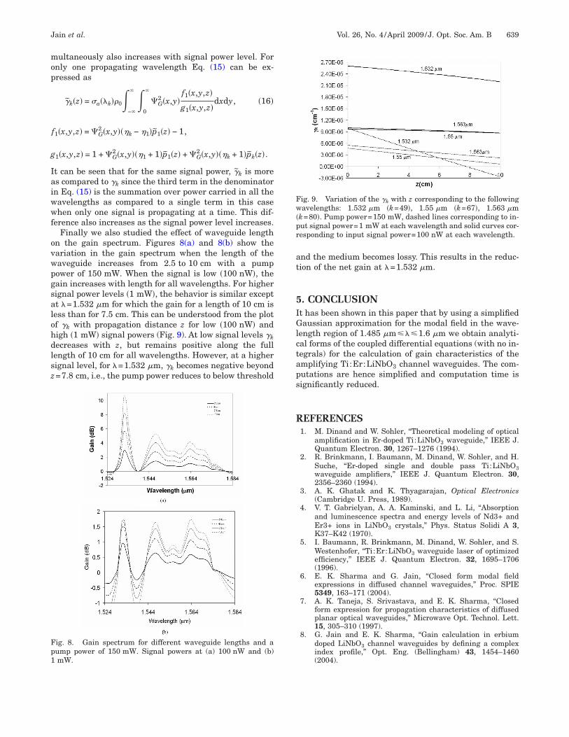
mop
g
Iaiwwf
ovwpgsalohdlsz
at
5IGlctaps
R
Fp1
Fw�pr
Jain et al. Vol. 26, No. 4 /April 2009 /J. Opt. Soc. Am. B 639
ultaneously also increases with signal power level. Fornly one propagating wavelength Eq. (15) can be ex-ressed as
�̃k�z� = a��k��0−�
� 0
�
G2 �x,y�
f1�x,y,z�
g1�x,y,z�dxdy, �16�
f1�x,y,z� = G2 �x,y���k − �1�p̃1�z� − 1,
1�x,y,z� = 1 + G2 �x,y���1 + 1�p̃1�z� + G
2 �x,y���k + 1�p̃k�z�.
t can be seen that for the same signal power, �̃k is mores compared to �k since the third term in the denominatorn Eq. (15) is the summation over power carried in all theavelengths as compared to a single term in this casehen only one signal is propagating at a time. This dif-
erence also increases as the signal power level increases.Finally we also studied the effect of waveguide length
n the gain spectrum. Figures 8(a) and 8(b) show theariation in the gain spectrum when the length of theaveguide increases from 2.5 to 10 cm with a pumpower of 150 mW. When the signal is low �100 nW�, theain increases with length for all wavelengths. For higherignal power levels �1 mW�, the behavior is similar exceptt �=1.532 �m for which the gain for a length of 10 cm isess than for 7.5 cm. This can be understood from the plotf �k with propagation distance z for low �100 nW� andigh �1 mW� signal powers (Fig. 9). At low signal levels �kecreases with z, but remains positive along the fullength of 10 cm for all wavelengths. However, at a higherignal level, for �=1.532 �m, �k becomes negative beyond=7.8 cm, i.e., the pump power reduces to below threshold
ig. 8. Gain spectrum for different waveguide lengths and aump power of 150 mW. Signal powers at (a) 100 nW and (b)
mW.nd the medium becomes lossy. This results in the reduc-ion of the net gain at �=1.532 �m.
. CONCLUSIONt has been shown in this paper that by using a simplifiedaussian approximation for the modal field in the wave-
ength region of 1.485 �m���1.6 �m we obtain analyti-al forms of the coupled differential equations (with no in-egrals) for the calculation of gain characteristics of themplifying Ti:Er:LiNbO3 channel waveguides. The com-utations are hence simplified and computation time isignificantly reduced.
EFERENCES1. M. Dinand and W. Sohler, “Theoretical modeling of optical
amplification in Er-doped Ti:LiNbO3 waveguide,” IEEE J.Quantum Electron. 30, 1267–1276 (1994).
2. R. Brinkmann, I. Baumann, M. Dinand, W. Sohler, and H.Suche, “Er-doped single and double pass Ti:LiNbO3waveguide amplifiers,” IEEE J. Quantum Electron. 30,2356–2360 (1994).
3. A. K. Ghatak and K. Thyagarajan, Optical Electronics(Cambridge U. Press, 1989).
4. V. T. Gabrielyan, A. A. Kaminski, and L. Li, “Absorptionand luminescence spectra and energy levels of Nd3+ andEr3+ ions in LiNbO3 crystals,” Phys. Status Solidi A 3,K37–K42 (1970).
5. I. Baumann, R. Brinkmann, M. Dinand, W. Sohler, and S.Westenhofer, “Ti:Er:LiNbO3 waveguide laser of optimizedefficiency,” IEEE J. Quantum Electron. 32, 1695–1706(1996).
6. E. K. Sharma and G. Jain, “Closed form modal fieldexpressions in diffused channel waveguides,” Proc. SPIE5349, 163–171 (2004).
7. A. K. Taneja, S. Srivastava, and E. K. Sharma, “Closedform expression for propagation characteristics of diffusedplanar optical waveguides,” Microwave Opt. Technol. Lett.15, 305–310 (1997).
8. G. Jain and E. K. Sharma, “Gain calculation in erbiumdoped LiNbO3 channel waveguides by defining a complexindex profile,” Opt. Eng. (Bellingham) 43, 1454–1460
ig. 9. Variation of the �k with z corresponding to the followingavelengths: 1.532 �m �k=49�, 1.55 �m �k=67�, 1.563 �m
k=80�. Pump power=150 mW, dashed lines corresponding to in-ut signal power=1 mW at each wavelength and solid curves cor-esponding to input signal power=100 nW at each wavelength.
(2004).

Simplified Gain Calculation In Erbium Doped LiNbO3 Waveguides
Amita Kapoor*a ,Geetika Jainb, Enakshi K. Sharma1c aDepartmentt. of Electronics, Shaheed Rajguru College of Applied Sciences for Women, University of Delhi
bDepartment of Electronics, Maharaja Agarsen College, University of Delhi. cDepartment of Electronic Science, University of Delhi South Campus, New Delhi -110021, INDIA
ABSTRACT
The combination of excellent electro-optical, acousto-optical and non-linear optical properties makes lithium niobate (LiNbO3) an attractive host material for integrated optical components such as electro-optical modulators, acousto-optically tunable wavelength filters and Bragg gratings. In the last few years Erbium doped LiNbO3 waveguide optical amplifiers (EDWA’s) have attracted increasing interest. The combination of the amplifying properties of erbium with the excellent acousto-optical and electro-optical properties of the waveguide substrate LiNbO3 allows the development of a whole class of new waveguide devices of higher functionality. The optical gain achievable in Ti:Er:LiNbO3 waveguides by optical pumping could compensate or even over compensate these scattering, absorption and insertion losses leading to “zero loss” devices with net optical gain. The different types of lasers and amplifiers can be combined with other active and passive devices on the same substrate to form integrated optical circuits (IOC’s) for a variety of applications in optical communications, sensing, signal processing and measurement techniques. The analysis of Er-doped diffused channel waveguides is, hence, required for design of amplifying integrated optical circuits in order to optimize the performance of these gain devices. The coupled differential equations, which govern the evolution of, pump power (1484nm), signal power (1485 to 1600nm) and amplified spontaneous emission, involve integrals which depend explicitly on the modal fields at the pump and signal wavelength in the diffused channel waveguide. In general, it is not possible to obtain analytical forms for the modal fields and propagation constant, hence, to obtain them various approximate or numerical methods (BPM, finite difference or finite element) are used. In this paper the modal field profiles obtained by the variational analysis are further approximated to an appropriately chosen Gaussian function, which leads to analytical forms of coupled differential equations with no integrals for the calculation of gain and ASE characteristics of the amplifying waveguide. Thus, computations are simplified and computation time is also reduced.
Keywords: Lithium niobate channel waveguide, Er doped waveguide, Gaussian approximation, amplified spontaneous emission (ASE).
1. INTRODUCTION The typical refractive index profile obtained by Titanium diffusion into LiNbO3 waveguides can be described as
( ) ( ) ⎟⎠⎞
⎜⎝⎛ −−∆+= 2
2
2222 expexp2, h
yw
xnnnyxn ss 0>y (1)
2cn= 0<y
where ns and nc are the substrate and cover layer indices, w and h are the half width and penetration depth of the index variation of diffused waveguide. Figure 1 shows the typical refractive index and the waveguide structure, x and y are the coordinates in the plane perpendicular to the waveguide axis, which is parallel to the propagation direction z. The wave propagation through such a structure is defined by Helmholtz equation1. Let the modal field for the above structure be represented by ),( yxΨ .Erbium is incorporated into the LiNbO3 lattice as Er3+ ions preferentially at Li+ sites6. Due to Stark effect, the 4f11 electron configuration of the ground state 4I15/2 splits into 8 doubly degenerate levels and the first excited state 4I13/2 splits into 7 Stark sublevels. Transition between both manifolds determines the optical absorption and hence amplification by stimulated emission in the wavelength range 1.44µm≤λ≤1.64µm. Excited state absorption (ESA) is weak for λp=1.484µm, hence it is the preferred pump for Er:LiNbO3. Furthermore for λp=1.484µm, the fabricated
1 Mail [email protected]
Physics and Simulation of Optoelectronic Devices XV, edited by Marek Osinski, Fritz Henneberger, Yasuhiko Arakawa,Proc. of SPIE Vol. 6468, 646808, (2007) · 0277-786X/07/$18 · doi: 10.1117/12.700001
Proc. of SPIE Vol. 6468 646808-1
Downloaded from SPIE Digital Library on 12 Sep 2010 to 122.162.62.21. Terms of Use: http://spiedl.org/terms
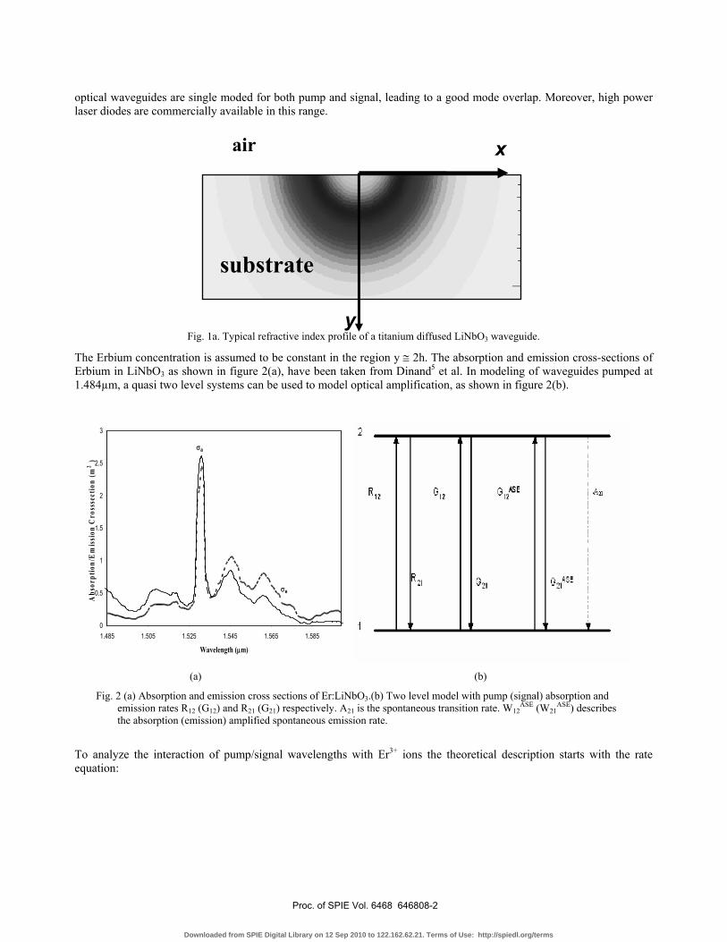
012 0SE12
V
substrate
air x
y
optical waveguides are single moded for both pump and signal, leading to a good mode overlap. Moreover, high power laser diodes are commercially available in this range.
Fig. 1a. Typical refractive index profile of a titanium diffused LiNbO3 waveguide.
The Erbium concentration is assumed to be constant in the region y ≅ 2h. The absorption and emission cross-sections of Erbium in LiNbO3 as shown in figure 2(a), have been taken from Dinand5 et al. In modeling of waveguides pumped at 1.484µm, a quasi two level systems can be used to model optical amplification, as shown in figure 2(b).
0
0.5
1
1.5
2
2.5
3
1.485 1.505 1.525 1.545 1.565 1.585
Wavelength (µm)
Abs
orpt
ion/
Em
issi
on C
ross
sect
ion
(m2
)
σa
σe
(a) (b)
Fig. 2 (a) Absorption and emission cross sections of Er:LiNbO3.(b) Two level model with pump (signal) absorption and emission rates R12 (G12) and R21 (G21) respectively. A21 is the spontaneous transition rate. W12
ASE (W21ASE) describes
the absorption (emission) amplified spontaneous emission rate.
To analyze the interaction of pump/signal wavelengths with Er3+ ions the theoretical description starts with the rate equation:
Proc. of SPIE Vol. 6468 646808-2
Downloaded from SPIE Digital Library on 12 Sep 2010 to 122.162.62.21. Terms of Use: http://spiedl.org/terms
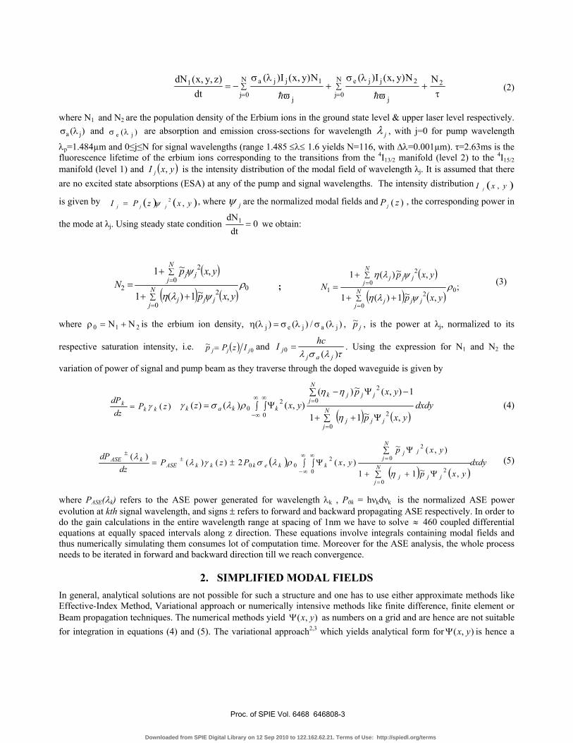
τ+
ϖ
λσ+
ϖ
λσ−= ∑∑
==
2N
0jj
2jjeN
0jj
1jja1 NN)y,x(I)(N)y,x(I)(dt
)z,y,x(dNhh
(2)
where N1 and N2 are the population density of the Erbium ions in the ground state level & upper laser level respectively. )( ja λσ and )( je λσ are absorption and emission cross-sections for wavelength jλ , with j=0 for pump wavelength
λp=1.484µm and 0≤j≤N for signal wavelengths (range 1.485 ≤λ≤ 1.6 yields N=116, with ∆λ=0.001µm). τ=2.63ms is the fluorescence lifetime of the erbium ions corresponding to the transitions from the 4I13/2 manifold (level 2) to the 4I15/2 manifold (level 1) and ( )yxI j , is the intensity distribution of the modal field of wavelength λj. It is assumed that there are no excited state absorptions (ESA) at any of the pump and signal wavelengths. The intensity distribution ( )yxI j ,
is given by ( ) ( )yxzPI jjj ,2ψ= , where jψ are the normalized modal fields and )( zP j , the corresponding power in
the mode at λj. Using steady state condition 0dt
dN1 = we obtain:
( )
( ) ( )02
0
2
02
,~1)(1
,~1ρ
ψλη
ψ
yxp
yxpN
jjjN
j
jjN
j
++
+=
∑
∑
=
= ;
( )
( ) ( );
,~1)(1
,~)(102
0
2
01 ρ
ψλη
ψλη
yxp
yxpN
jjjN
j
jjjN
j
++
+=
∑
∑
=
=
where 210 NN +=ρ is the erbium ion density, )(/)()( jajej λσλσ=λη , jp~ , is the power at λj, normalized to its
respective saturation intensity, i.e. ( ) 0~
jjj IzPp = and τλσλ )(0
jajj
hcI = . Using the expression for N1 and N2 the
variation of power of signal and pump beam as they traverse through the doped waveguide is given by
)( zPdz
dPkk
k γ= ( ) ( )
dxdyyxp
yxpyxz
jjjN
j
N
jjjjk
kkak,~11
1),(~)(),()()(
2
0
0
2
0
20
Ψ+∑+
∑ −Ψ−
∫ ∫ Ψ=
=
=∞
∞−
∞
η
ηηρλσγ (4)
( )( ) ( )
dxdyyxp
yxpyxPzP
dzdP
jjjN
j
N
jjj
kkekkkASEkASE ∫ ∫
Ψ+∑+
∑ ΨΨ±=
∞
∞−
∞
=
=±±
0 2
0
0
2
200
,~11
),(~
),(2)()()(
ηρλσγλ
λ (5)
where PASE(λk) refers to the ASE power generated for wavelength λk , P0k = hνkdνk is the normalized ASE power evolution at kth signal wavelength, and signs ± refers to forward and backward propagating ASE respectively. In order to do the gain calculations in the entire wavelength range at spacing of 1nm we have to solve ≈ 460 coupled differential equations at equally spaced intervals along z direction. These equations involve integrals containing modal fields and thus numerically simulating them consumes lot of computation time. Moreover for the ASE analysis, the whole process needs to be iterated in forward and backward direction till we reach convergence.
2. SIMPLIFIED MODAL FIELDS In general, analytical solutions are not possible for such a structure and one has to use either approximate methods like Effective-Index Method, Variational approach or numerically intensive methods like finite difference, finite element or Beam propagation techniques. The numerical methods yield ),( yxΨ as numbers on a grid and are hence are not suitable for integration in equations (4) and (5). The variational approach2,3 which yields analytical form for ),( yxΨ is hence a
(3)
Proc. of SPIE Vol. 6468 646808-3
Downloaded from SPIE Digital Library on 12 Sep 2010 to 122.162.62.21. Terms of Use: http://spiedl.org/terms
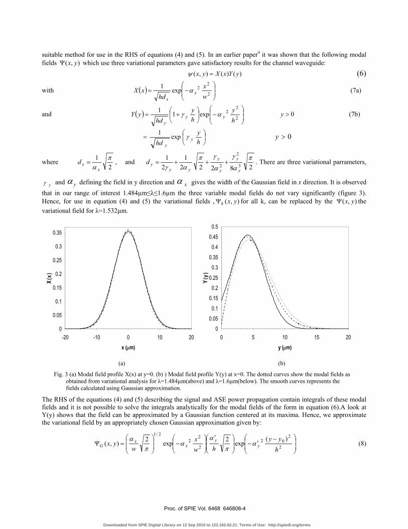
suitable method for use in the RHS of equations (4) and (5). In an earlier paper4 it was shown that the following modal fields ),( yxΨ which use three variational parameters gave satisfactory results for the channel waveguide:
)()(),( yYxXyx =ψ (6)
with ( ) ⎟⎟⎠
⎞⎜⎜⎝
⎛−=
2
22exp1
wx
hdxX x
x
α (7a)
and ( ) ⎟⎟⎠
⎞⎜⎜⎝
⎛−⎟
⎠
⎞⎜⎝
⎛ +=2
22exp11
hy
hy
hdyY yy
y
αγ 0>y (7b)
⎟⎠⎞
⎜⎝⎛=
hy
hdy
y
γexp1 0>y
where 2
1 πα x
xd = , and 28222
12
13
2
2π
α
γ
α
γπαγ y
y
y
y
yyyd +++= . There are three variational parrameters,
yγ and yα defining the field in y direction and xα gives the width of the Gaussian field in x direction. It is observed that in our range of interest 1.484µm≤λ≤1.6µm the three variable modal fields do not vary significantly (figure 3). Hence, for use in equation (4) and (5) the variational fields , ),( yxkΨ for all k, can be replaced by the ),( yxΨ the variational field for λ=1.532µm.
0
0.05
0.1
0.15
0.2
0.25
0.3
0.35
-20 -10 0 10 20
x (µm)
X(x)
0
0.05
0.1
0.15
0.2
0.25
0.3
0.35
0.4
0.45
0.5
0 5 10 15 20
y (µm)
Y(y)
(a) (b)
Fig. 3 (a) Modal field profile X(x) at y=0. (b) ) Modal field profile Y(y) at x=0. The dotted curves show the modal fields as obtained from variational analysis for λ=1.484µm(above) and λ=1.6µm(below). The smooth curves represents the fields calculated using Gaussian approximation.
The RHS of the equations (4) and (5) describing the signal and ASE power propagation contain integrals of these modal fields and it is not possible to solve the integrals analytically for the modal fields of the form in equation (6).A look at Y(y) shows that the field can be approximated by a Gaussian function centered at its maxima. Hence, we approximate the variational field by an appropriately chosen Gaussian approximation given by:
⎟⎟⎠
⎞⎜⎜⎝
⎛ −′−⎟
⎟⎠
⎞⎜⎜⎝
⎛ ′⎟⎟⎠
⎞⎜⎜⎝
⎛−⎟
⎟⎠
⎞⎜⎜⎝
⎛=Ψ
2
202
2
22
2/1)(
exp2exp2),(h
yyhw
xw
yx yy
xx
G απ
αα
πα
(8)
Proc. of SPIE Vol. 6468 646808-4
Downloaded from SPIE Digital Library on 12 Sep 2010 to 122.162.62.21. Terms of Use: http://spiedl.org/terms
where ⎟⎠⎞⎜
⎝⎛ −+= yyy
y
hy αγαα
220 2
2 is the y value for which Y(y) variational field has maximum value, the
variational parameters xα , yα and yγ correspond to λ=1.532µm.
To obtain the value of yα ′ we maximize the overlap between the Y(y) field and the Gaussian field, i.e, we maximize the integral
dyh
yyhh
yhdh
yI y
yy
yy ⎟
⎟⎠
⎞⎜⎜⎝
⎛ −′−⎟
⎟⎠
⎞⎜⎜⎝
⎛ ′⎟⎟⎠
⎞⎜⎜⎝
⎛−
⎟⎟⎟
⎠
⎞
⎜⎜⎜
⎝
⎛⎟⎠
⎞⎜⎝
⎛ += ∫∞
2
202
2/1
2
22
0
)(exp2exp11 α
π
ααγ
Figure 3 shows the field as obtained from variational analysis and the Gaussian approximated fields in both x and y directions respectively. It can be observed that by appropriately choosing the Gaussian approximation we are able to retain the shape of modal field and at the same time the RHS integrals of equations (4) and (5) can now be solved analytically, as shown in section 3.
3. SIMPLIFIED GAIN CALCULATIONS On using the approximated Gaussian modal fields the gain coefficient γk for signal of wavelength λk and the ASE power calculations as defined in equations 4 and 4 of section 1, can be simplified as
( ) ( )dxdy
yxp
yxpyxz
GjjN
j
N
jGjjk
Gkak,~11
1),(~)(),()()(
2
0
0
2
0
20
Ψ+∑+
∑ −Ψ−
∫ ∫ Ψ=
=
=∞
∞−
∞
η
ηηρλσγ (9)
( )( ) ( )
dxdyyxp
yxpyxPzP
dzdP
GjjN
j
N
jGj
GkekkkASEkASE ∫ ∫
Ψ+∑+
∑ ΨΨ±=
∞
∞−
∞
=
=±±
0 2
0
0
2
200
,~11
),(~
),(2)()()(
ηρλσγλ
λ (10)
Transforming coordinated from [x,y] plane to ],[ ηζ plane such that w
xxαζ 2= and
hyyy )(
2 0−′=
αη the Gaussian
modal field can be re-written as )](exp[),( 22 ηζηζ +−=Ψ AG with constant π
αα
whA yx ′=
2. The above expressions then
become:
( )ηζ
ηηζ
ηηηζηζ
πρλσ
γ ddpA
pAAz
jjN
j
N
jjjk
kak ~1)](exp[1
1~)()](exp[)](exp[
)()(
0
22
0
22
220
+∑+−+
∑ −−+−
∫ ∫ +−=
=
=∞
∞−
∞
∞−
( )( )
ηζηηζ
ηζηζ
πρλσ
γλλ
ddpA
pAA
PzP
dzdP
jjN
j
N
jj
kekkkASE
kASE ∫ ∫+∑+−+
∑+−+−±=
∞
∞−
∞
∞−
=
=±±
~1)](exp[1
~)](exp[)](exp[
2)()(
)(
0
22
0
22
2200
The limits of η field have been taken as [-∞,∞] since the modal fields are negligible after y<0. Now we transform into polar coordinates [r,θ], resulting in
( )θ
η
ηη
πρλσ
γπ
rdrdprA
prArAz
jjN
j
N
jjjk
kak ~1]exp[1
1~)(]exp[]exp[
)()(
0
2
0
22
0 0
20
+∑−+
∑ −−−
∫ ∫ −=
=
=∞
Proc. of SPIE Vol. 6468 646808-5
Downloaded from SPIE Digital Library on 12 Sep 2010 to 122.162.62.21. Terms of Use: http://spiedl.org/terms
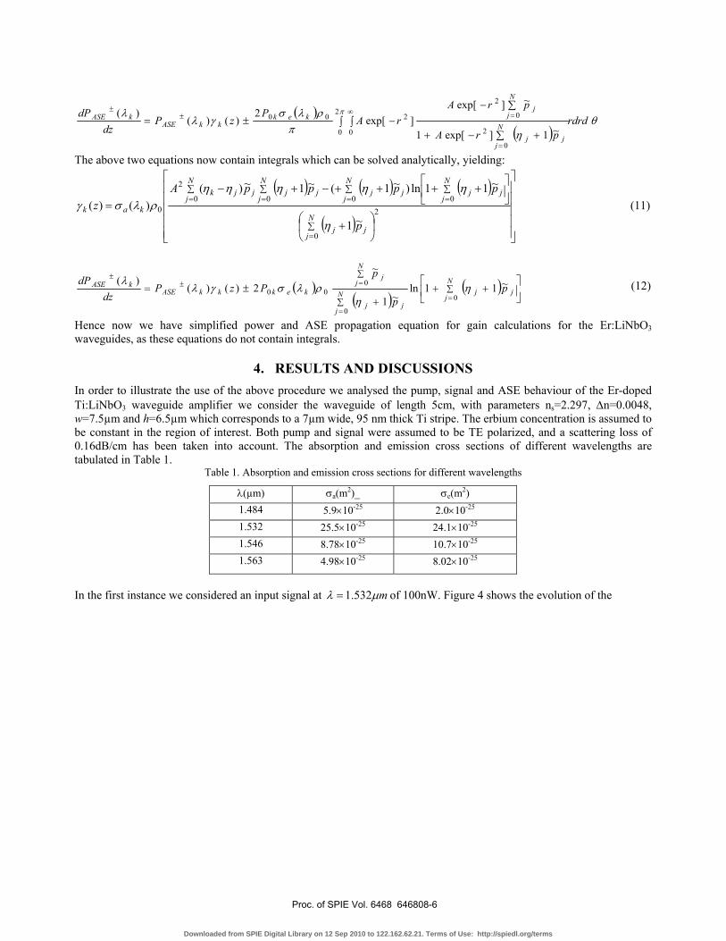
( )( )
θηπ
ρλσγλ
λ πrdrd
prA
prArA
PzP
dzdP
jjN
j
N
jj
kekkkASE
kASE ∫ ∫+∑−+
∑−−±=
∞
=
=±± 2
0 0
0
2
0
2
200
~1]exp[1
~]exp[]exp[
2)()(
)(
The above two equations now contain integrals which can be solved analytically, yielding:
( ) ( ) ( )
( )⎥⎥⎥⎥⎥
⎦
⎤
⎢⎢⎢⎢⎢
⎣
⎡
⎟⎠
⎞⎜⎝
⎛ +
⎥⎦
⎤⎢⎣
⎡ ++++−+−=
∑
∑ ∑∑∑
=
= ===
2
0
0 000
2
0~1
~11ln)~1(~1~)()()(
jjN
j
N
jjj
N
jjj
N
jjj
N
jjjk
kak
p
ppppAz
η
ηηηηηρλσγ (11)
( )( )
( ) ⎥⎦
⎤⎢⎣
⎡++
+±= ∑
∑
∑
=
=
=±±
jjN
jjj
N
j
N
jj
kekkkASEkASE p
p
pPzP
dzdP ~11ln
~1
~
2)()()(
0
0
000 η
ηρλσγλ
λ (12)
Hence now we have simplified power and ASE propagation equation for gain calculations for the Er:LiNbO3 waveguides, as these equations do not contain integrals.
4. RESULTS AND DISCUSSIONS In order to illustrate the use of the above procedure we analysed the pump, signal and ASE behaviour of the Er-doped Ti:LiNbO3 waveguide amplifier we consider the waveguide of length 5cm, with parameters ns=2.297, ∆n=0.0048, w=7.5µm and h=6.5µm which corresponds to a 7µm wide, 95 nm thick Ti stripe. The erbium concentration is assumed to be constant in the region of interest. Both pump and signal were assumed to be TE polarized, and a scattering loss of 0.16dB/cm has been taken into account. The absorption and emission cross sections of different wavelengths are tabulated in Table 1.
Table 1. Absorption and emission cross sections for different wavelengths
λ(µm) σa(m2)_ σe(m2) 1.484 5.9×10⁻²⁵ 2.0×10⁻²⁵ 1.532 25.5×10⁻²⁵ 24.1×10⁻²⁵ 1.546 8.78×10⁻²⁵ 10.7×10⁻²⁵ 1.563 4.98×10⁻²⁵ 8.02×10⁻²⁵
In the first instance we considered an input signal at mµλ 532.1= of 100nW. Figure 4 shows the evolution of the
Proc. of SPIE Vol. 6468 646808-6
Downloaded from SPIE Digital Library on 12 Sep 2010 to 122.162.62.21. Terms of Use: http://spiedl.org/terms
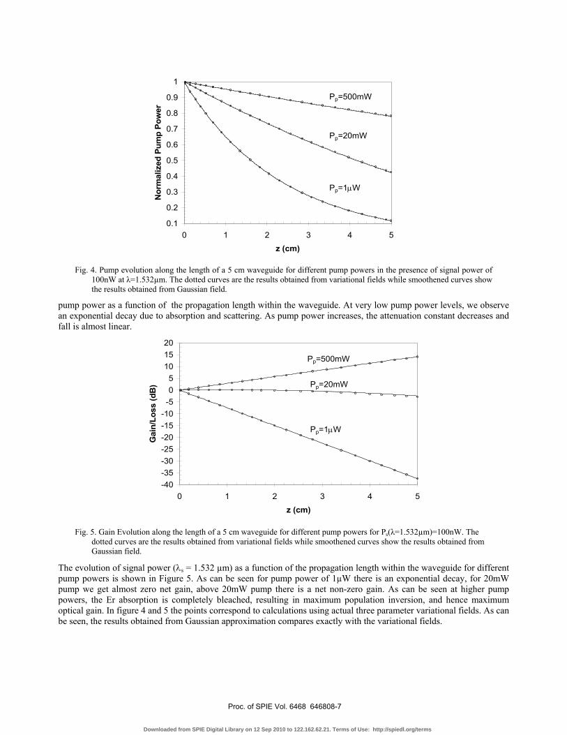
0.1
0.2
0.3
0.4
0.5
0.6
0.7
0.8
0.9
1
0 1 2 3 4 5z (cm)
Nor
mal
ized
Pum
p Po
wer
Pp=500mW
Pp=20mW
Pp=1µW
Fig. 4. Pump evolution along the length of a 5 cm waveguide for different pump powers in the presence of signal power of
100nW at λ=1.532µm. The dotted curves are the results obtained from variational fields while smoothened curves show the results obtained from Gaussian field.
pump power as a function of the propagation length within the waveguide. At very low pump power levels, we observe an exponential decay due to absorption and scattering. As pump power increases, the attenuation constant decreases and fall is almost linear.
-40-35-30-25-20-15-10-505
101520
0 1 2 3 4 5z (cm)
Gai
n/Lo
ss (d
B)
Pp=500mW
Pp=20mW
Pp=1µW
Fig. 5. Gain Evolution along the length of a 5 cm waveguide for different pump powers for Ps(λ=1.532µm)=100nW. The
dotted curves are the results obtained from variational fields while smoothened curves show the results obtained from Gaussian field.
The evolution of signal power (λs = 1.532 µm) as a function of the propagation length within the waveguide for different pump powers is shown in Figure 5. As can be seen for pump power of 1µW there is an exponential decay, for 20mW pump we get almost zero net gain, above 20mW pump there is a net non-zero gain. As can be seen at higher pump powers, the Er absorption is completely bleached, resulting in maximum population inversion, and hence maximum optical gain. In figure 4 and 5 the points correspond to calculations using actual three parameter variational fields. As can be seen, the results obtained from Gaussian approximation compares exactly with the variational fields.
Proc. of SPIE Vol. 6468 646808-7
Downloaded from SPIE Digital Library on 12 Sep 2010 to 122.162.62.21. Terms of Use: http://spiedl.org/terms
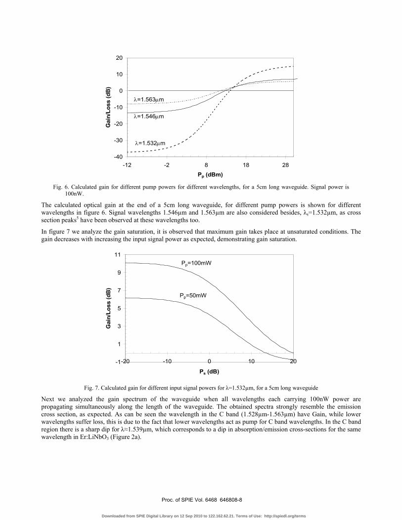
-40
-30
-20
-10
0
10
20
-12 -2 8 18 28Pp (dBm)
Gai
n/Lo
ss (d
B)
λ=1.532µm
λ=1.563µm
λ=1.546µm
Fig. 6. Calculated gain for different pump powers for different wavelengths, for a 5cm long waveguide. Signal power is
100nW.
The calculated optical gain at the end of a 5cm long waveguide, for different pump powers is shown for different wavelengths in figure 6. Signal wavelengths 1.546µm and 1.563µm are also considered besides, λs=1.532µm, as cross section peaks5 have been observed at these wavelengths too.
In figure 7 we analyze the gain saturation, it is observed that maximum gain takes place at unsaturated conditions. The gain decreases with increasing the input signal power as expected, demonstrating gain saturation.
-1
1
3
5
7
9
11
-20 -10 0 10 20
Ps (dB)
Gai
n/Lo
ss (d
B)
Pp=100mW
Pp=50mW
Fig. 7. Calculated gain for different input signal powers for λ=1.532µm, for a 5cm long waveguide
Next we analyzed the gain spectrum of the waveguide when all wavelengths each carrying 100nW power are propagating simultaneously along the length of the waveguide. The obtained spectra strongly resemble the emission cross section, as expected. As can be seen the wavelength in the C band (1.528µm-1.563µm) have Gain, while lower wavelengths suffer loss, this is due to the fact that lower wavelengths act as pump for C band wavelengths. In the C band region there is a sharp dip for λ≈1.539µm, which corresponds to a dip in absorption/emission cross-sections for the same wavelength in Er:LiNbO3 (Figure 2a).
Proc. of SPIE Vol. 6468 646808-8
Downloaded from SPIE Digital Library on 12 Sep 2010 to 122.162.62.21. Terms of Use: http://spiedl.org/terms
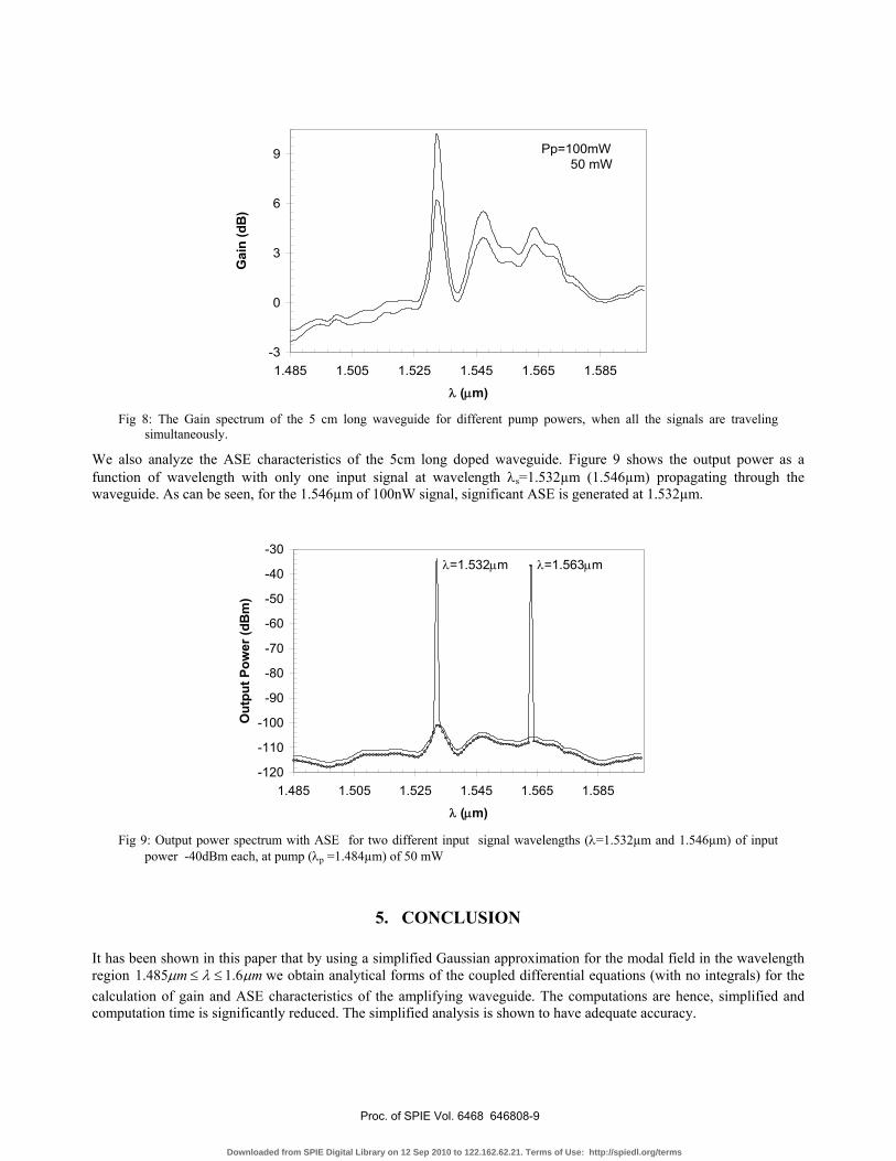
-3
0
3
6
9
1.485 1.505 1.525 1.545 1.565 1.585
λ (µm)
Gai
n (d
B)
Pp=100mW 50 mW
Fig 8: The Gain spectrum of the 5 cm long waveguide for different pump powers, when all the signals are traveling
simultaneously.
We also analyze the ASE characteristics of the 5cm long doped waveguide. Figure 9 shows the output power as a function of wavelength with only one input signal at wavelength λs=1.532µm (1.546µm) propagating through the waveguide. As can be seen, for the 1.546µm of 100nW signal, significant ASE is generated at 1.532µm.
-120
-110
-100
-90
-80
-70
-60
-50
-40
-30
1.485 1.505 1.525 1.545 1.565 1.585
λ (µm)
Out
put P
ower
(dB
m)
λ=1.532µm λ=1.563µm
Fig 9: Output power spectrum with ASE for two different input signal wavelengths (λ=1.532µm and 1.546µm) of input
power -40dBm each, at pump (λp =1.484µm) of 50 mW
5. CONCLUSION It has been shown in this paper that by using a simplified Gaussian approximation for the modal field in the wavelength region mm µλµ 6.1485.1 ≤≤ we obtain analytical forms of the coupled differential equations (with no integrals) for the calculation of gain and ASE characteristics of the amplifying waveguide. The computations are hence, simplified and computation time is significantly reduced. The simplified analysis is shown to have adequate accuracy.
Proc. of SPIE Vol. 6468 646808-9
Downloaded from SPIE Digital Library on 12 Sep 2010 to 122.162.62.21. Terms of Use: http://spiedl.org/terms

REFERENCES
1. A.K. Ghatak and K. Thyagrajan, “Optical Electronics” , Cambridge University press, Cambridge England 1989 2. E.K. Sharma and Geetika Jain, Closed form modal field expressions in diffused channel waveguides,
Proceedings of SPIE, Vol. No. 5349, (2004) 3. Ashmeet K. Taneja, Sangeeta Srivastava and Enakshi Khular Sharma, Closed form expression for propagation
characteristics of diffused planar optical waveguides, Microwave and Opt. tech. Lett. 15,pp. 305-310, (1997). 4. Geetika Jain and E. K. Sharma, Gain Calculation in Erbium Doped LiNbO3 Channel Waveguides by Defining a
Complex Index Profile, Optical Engineering. 43, 1454-1450 (2004). 5. Manfred Dinand, Wolfgang Sohler, Theoretical modeling of optical amplification in Er-doped Ti: LiNbO3
waveguide , IEEE J. Quantum Electron 30, pp. 1267-1276, (1994). 6. V.T.Gabrielyan, A.A. Kaminski, and L. Li, Absorption and Luminscence spectra and energy levels of Nd3+
and Er3+ ions in LiNbO3 crystals, Phys. Stat. Sol. (a), 3, K37,1970. 7. R. Brinkmann, I. Baumann, Manfred Dinand, Wolfgang Sohler, H. Suche, Er-doped single and double pass Ti:
LiNbO3 waveguide amplifiers, J. Quantum Electron. 30, 2356, (1994).
Proc. of SPIE Vol. 6468 646808-10
Downloaded from SPIE Digital Library on 12 Sep 2010 to 122.162.62.21. Terms of Use: http://spiedl.org/terms

Saturation characteristics of InGaAsP-InP bulk SOA
Amita Kapoor*a, Enakshi K. Sharmab, Wolfgang Freudec and Juerg Leutholdc
aShaheed Rajguru College of Applied Sciences for Women, University of Delhi, India; bDept. of Electronic Sciences, University of Delhi South Campus, New Delhi, India;
cInstitute of Photonics and Quantum Electronics, Karlsruhe Institute of Technology, Karlsruhe, Germany
ABSTRACT
Semiconductor optical amplifiers (SOAs) can be used as linear in-line amplifiers for extended-reach passive optical networks, or as gain/phase-switchable devices. For these applications, gain, bandwidth and saturation power are important. The saturation power can be increased by decreasing the confinement factor and by increasing the length such that the overall gain remains constant. In this paper we investigate the saturation characteristics of 1.55μm InGaAsP-InP bulk SOA. We do so by using the physically based simulation tool ATLAS.
The simulation tool ATLAS supports simulation of semiconductor lasers only, however making the mirror reflectivities small, the lasing threshold is increased such that lasers are essentially reduced to amplifiers. Next, for investigating the saturation characteristics of SOA, the amplifier gain should be influenced by injecting an optical light power. However, ATLAS cannot simulate the required source directly. Instead, we use in the electron rate equation simultaneously two competing independent models for spontaneous radiative recombination, namely the so-called general model (total recombination rate pBnT with bimolecular recombination coefficient B, electron and hole concentrations nT and p) and the standard model for recombination due to amplified spontaneous emission into the mode under consideration (determined by the product of Fermi functions for electrons and holes). In the photon rate equation, only the standard model is used. We then increase B, and thus simulate a decrease of the carrier concentration that would physically result from an external optical signal. We show that under conditions of constant injection current and device length an n-doping (p-doping) of the active layer increases (decreases) the input saturation power. In addition we observe that for constant injection current and amplifier gain, a p-doping (n-doping) of the active layer increases (decreases) both the input and output saturation powers because of an reduced (slightly increased) Auger-dominated carrier lifetime.
Keywords: Semiconductor optical amplifiers, p-doping, n-doping, gain saturation, ATLAS simulation
1. INTRODUCTION For the last few years, telecommunication institutes around the world have shown strong interest in semiconductor optical amplifiers (SOA). On one hand, with photonics moving near to end users, SOAs are being explored as in-line amplifiers or power boosters in metropolitan area networks, with a tough competition between bulk SOAs, quantum well (QW) SOAs and quantum dot (QD) SOAs1-3. On the other hand, nonlinearities of SOA can be exploited yielding means for optical data processing1-3. For a good in-line amplifier, the desired properties are high gain, high bandwidth, low polarization sensitivity, and high saturation power, while for optical signal processing low saturation power and a fast recovery time are desired.
In a typical SOA the active gain region is sandwiched between a p-doped and an n-doped cladding layer. The p and n-doped cladding regions have a larger band gap than the gain region. The p-n junction is forward biased, resulting in hole (electron) injection from the p-doped (n-doped) cladding into the gain region. Under proper biasing conditions, a population inversion occurs in the active region, a condition which is necessary for the amplification of light.
Physics and Simulation of Optoelectronic Devices XVIII, edited byBernd Witzigmann, Fritz Henneberger, Yasuhiko Arakawa, Marek Osinski, Proc. of SPIE
Vol. 7597, 75971I · © 2010 SPIE · CCC code: 0277-786X/10/$18 · doi: 10.1117/12.842350
Proc. of SPIE Vol. 7597 75971I-1
Downloaded from SPIE Digital Library on 12 Sep 2010 to 122.162.62.21. Terms of Use: http://spiedl.org/terms
Several models have been developed in the past to simulate SOAs1, 2, 5-7. Most frequently, rate equations are solved, i.e., time dependent coupled differential equations for carriers and photons. Numerically, either the carrier density is averaged over the entire length of the device, or the SOA is subdivided into small sections. However, while these models are able to give a reasonable approximation of the SOA behavior in certain operating regions, they do not provide insight into the actual physics relevant for the device. In order to improve this situation, we use the material parameter-based simulation tool ATLAS (Silvaco) for predicting the dependence of saturation properties and gain recovery of bulk SOA and for different doping levels of the active layer.
1.1 SOA physics
In an SOA electrons, holes and photons interact. These interactions result in a change in carrier and photon densities, and thus determine the behavior of an SOA in response to the applied optical field at a particular bias current. For the amplification of light, it is necessary to achieve population inversion in the active medium. The external current source injects charge carriers into the active region. Various radiative processes (namely spontaneous emission, stimulated emission and absorption) and non-radiative mechanisms (namely Auger recombination and Shockley Read Hall recombination) cause the recombination and generation of these carriers in the active region. Moreover, the carriers exert Coulomb forces on each other and have intraband interactions (namely free carrier absorption, band gap narrowing and Burstein-Moss effect) as well. A detailed model of an SOA requires understanding of both inter and intra-band interactions. The optical signal (scalar electric field E ) influences the potential � and thereby the energy position of the conduction and valence band edges. The propagation of the electric field E inside the amplifier is determined by the scalar wave equation in Cartesian coordinates (transverse directions x, y, propagation direction z),
22
2 2
( , )0r x y EE
c t� �
� � ��
, (1)
where ),( yxr� is the dielectric constant of the medium and c is the vacuum speed of light. The dielectric constant is related to the optical gain5 mg by
� � , ,2 ( , )
( , ) j j b a fc n fc pb mr b H
w w
n n pn g x yx y nk k
�
� �� � � � � , (2)
where bn is the bulk refractive index, H is the linewidth broadening factor (Henry factor), a is the bulk absorption coefficient, and nfc, , pfc, are free carrier absorption coefficients for electron and holes, respectively. The quantity kw represents the free space wave vector.
To determine the rate by which the electron density Tn , the hole density p and the total photon density totS will change, we need to consider different recombination and generation mechanisms within the semiconductor. Let
sp TR Bn p� be the spontaneous emission recombination rate, sigR the recombination rate due to the presence of an optical signal, ASER the recombination rate due to amplified spontaneous emission, AugerR the recombination rate due to
Auger recombination, and SRHR the recombination rate due to Shockley Read Hall recombination. If pn JJJ���
�� is the total current density consisting of electron and hole current density, then the rate by which the density of electrons, holes and photons change, is
� � SRH Auger sp ASE sig1 divT
nn J R R R R Rt e
�� � � � � �
�
�, (3)
� � SRH Auger sp ASE sig1 div p
p J R R R R Rt e�
� � � � � � ��
�, (4)
Proc. of SPIE Vol. 7597 75971I-2
Downloaded from SPIE Digital Library on 12 Sep 2010 to 122.162.62.21. Terms of Use: http://spiedl.org/terms
tot tottot sp
ph
m mm
g mdS Sv g S QRdt �
� � � , (5)
Here, gv is the group velocity, � � 2 21ph , , mirr( , ) d d ( , ) d dg a fc n fc pv E x y x y n p E x y x y� � � � � ��� �� the photon
lifetime, mirr the mirror losses (if any), and tot sig ASEm m mS S S� � is the total photon density in longitudinal mode m, which
results from the optical signal input as well as from amplified spontaneous emission. In (3) and (4) the first term refers to the increase in the carrier density through the injection current. The terms in the first parentheses refer to the decrease in the carrier density due to the combined effect of radiative (only spontaneous) and non-radiative recombinations. The third term finally corresponds to the decrease in the carrier density due to stimulated emission of carriers induced by the presence of photons. These three terms determine the rate at which the carrier density changes with time.
Equation (5) describes the rate of the photon density change. The terms in (3) and (4), which cause a change in the carrier density due to interaction with photons, correspond to a quantity in (5). The first term on the right hand side of (5) accounts for the gain (loss) in the photon density due to stimulated emission (absorption) of photons; this term corresponds to the third term in (5) with a multiplicative factor . This is so, because the carriers and the photons occupy different but overlapping regions: Only the fraction of the optical electric field � yxE , which is confined to the active region contributes to a change in carrier density. The confinement factor is defined by
2
0 0
2
( , ) d d
( , ) d d
d w
E x y x y
E x y x y� �
�� ��
�� �
� �, (6)
where w is the width and d the height of the active layer. The second term in (5) takes care of the different photon loss mechanisms, and the last term corresponds to an increase in photons due to spontaneous emission. The factor Q , also known as emission factor, describes the small fraction of the total spontaneously emitted photons that contribute to the guided longitudinal modal field under consideration.
1.2 Gain saturation and gain recovery
When a high-power (Pin) optical input signal is present, the carriers in the active region are depleted resulting in a decrease of the optical gain. This is referred to as gain saturation: The larger Pin becomes, the closer the output power Pout comes to Pin so that the gain G = Pout / Pin approaches unity (G � 1). The input optical power at which the gain of the amplifier reduces to half of the small signal gain is known as the input saturation power sat
inP 1-3, where G0 is the small-signal gain without saturation (unsaturated gain), Ps defines the saturation parameter, gm, gm0 are the material gain and the unsaturated material gain, respectively, and L is the total length of the SOA:
� LgGwda
hfPGP
P mle
sssat
in 000
exp,1,22ln2
�
��
��
(7)
The corresponding output saturation power will be
sat sat 0out 0 in
0
2 ln 22
sP GP G P
G� �
�, (8)
where h f is the photon energy, � spAugerSRHe RRR ���1� is the spontaneous carrier lifetime, and al the differential gain. The saturation parameter Ps is not a constant, but depends through �eff and al weakly on the carrier density and therefore on the input power. The asymptotic gain saturation of an SOA can be modeled by approximating the dependency Pout(Pin) by two straight lines, Figure 1,
Proc. of SPIE Vol. 7597 75971I-3
Downloaded from SPIE Digital Library on 12 Sep 2010 to 122.162.62.21. Terms of Use: http://spiedl.org/terms
forfor
in inout
in in
a P P dP
b P c P d��
� � � ��. (9)
The parameters cba ,, are to be determined by a least squares fit to actually calculated curves, and d results from the intersection of the straight lines. From (7) we see that the saturation power decreases with carrier lifetime eff� and differential gain la , and that it increases with the effective interaction cross-section /wd . The dependence of the saturation power on the unsaturated gain 0G is more involved. It is easy to see that the input saturation power decreases with increasing 0G , and that for high gain 0 1G �� the output saturation power is almost independent of 0G .
Figure 1: Gain saturation of an SOA section of length l. n = L / l sections are concatenated for a total SOA length L.
Relations for the straight-line approximations are written in the graph. If n SOA sections are concatenated, the substitution l � nl has to be made, see equation (14) in the next section.
Closely related to the phenomenon of gain saturation is gain recovery, i.e. the restoration of the depleted carriers to their steady state values. Several processes are involved8. Fast intraband scattering and carrier heating (picosecond scale) is followed by a slow filling of depleted carrier states via the injected current. Since gain is coupled with carrier density, these effects can be observed in the temporal evolution of the gain. Generally, the gain recovery is defined in terms of 10-90% recovery time rect . It is the time needed for the amplifier gain ( LgmeG � ) to rise from 10% to 90% of the saturation. According to Joyner et al.9, the recovery time rec� depends on the effective carrier lifetime
� sigASEspAugerSRHeff RRRRR �����1� .
The gain saturation and gain recovery behavior of SOA is important not only for linear amplification but also for nonlinear signal processing tasks. Depending on the specific task, the design of an SOA is modified to optimize the performance. For example, for an SOA as a linear amplifier the requirements are high gain, high saturation power, low -factor and fast recovery. For SOA as wavelength converters the desired properties are low saturation power and fast recovery, and, if relying on cross-phase modulation, also a large -factor.
In this paper we investigate the effect of doping of the active layer on the SOA performance. There have been various studies regarding the effect of doping of the active layer on semiconductor lasers10-12. It has been reported that moderate doping (~1018 cm-3) increases the differential gain la and the bandwidth, but decreases the spontaneous lifetime of carriers and the threshold current. There are detailed data of the effect of both p-doping and n-doping on the behavior of QD SOAs published by Qasaimeh13, who reported that p-doping increases the unsaturated amplifier gain, while n-doping improves the linearity of the amplifier by increasing the current density to reach gain saturation. Similar effects of p-doping are reported by Neilson et al.14 for MQW SOAs.
Proc. of SPIE Vol. 7597 75971I-4
Downloaded from SPIE Digital Library on 12 Sep 2010 to 122.162.62.21. Terms of Use: http://spiedl.org/terms
2. ATLAS SIMULATION
ATLAS is a physically based device simulation tool with the capability to include various physical effects important for semiconductor lasers15. Using ATLAS it is possible to predict the electrical and optical characteristics that are associated with specific physical structures and bias conditions. ATLAS supports the implementation of semiconductor lasers but has no built-in support for SOAs. An SOA is essentially a semiconductor laser with low mirror reflectivities1-3, 16. Thus, by reducing the mirror reflectivities, one is able to model an SOA. This can provide us with the information regarding gain and ASE spectrum of the SOA without any optical input signal. However, this information is insufficient. For a complete characterization of an SOA it is important to know how gain and carrier densities change (gain saturation and gain recovery) in response to the optical signal. Unfortunately, ATLAS has no support for an optical input. The work-around is to change the radiative recombination parameter B for implementing the effect of an optical source on the carrier numbers17. In ATLAS, there is no true optical input, and a stimulated recombination term due to an optical signal
sigR (which is necessary to describe a laser) will not be used; thus the carrier rate equation (3) can be rewritten as:
� SRH Auger sp ASE1 divT
nn J R R R Rt e
�� � � � �
�
� (10)
Here sp TR Bn p� corresponds to the radiative recombination rate due to spontaneous emission. If we change the radiative recombination parameter from B to BB �� , then we have
� SRH Auger ASE1 divT
n T Tn J R R Bn p R B n pt e
��
� � � � � ��
� (11)
Thus, an increase in the radiative recombination parameter by B� results in a reduction of the carrier density in a similar fashion as if for an optical input signal. Hence, we implement the effect of a virtual optical input power by comparing (11) and (3),
sig TR B n p�� . (12)
We subdivide the total SOA length L into n = L / l small sections of length l. From (12), we then derive an expression for the virtual input signal power to a small section in terms of the change in the radiative recombination parameter B� , the electron and hole concentration, and the reduced material gain mg ,
in e mg lT
m
B n p wdP hfg
� � �
. (13)
Hence, for small sections of the amplifier it is possible to obtain an analytical expression relating the (unphysical) change in B with the virtual optical input power.
In order to model gain saturation we need to determine the parameters cba ,, (9) from a fit to the curve Pout = Pout(Pin) that is found by simulation. This relation is for a small section of length l, and n such concatenated sections constitute the whole SOA. Therefore, after an SOA length nlL � the output and input optical power will be related by the expression (see also caption to Figure 1):
��
���
���� )(
)()(
ninin
ninin
nn
out dPcnPbdPPaP (14)
After n SOA sections, the quantity )(nd is the intersection point of the two linear relations given in (14).
Proc. of SPIE Vol. 7597 75971I-5
Downloaded from SPIE Digital Library on 12 Sep 2010 to 122.162.62.21. Terms of Use: http://spiedl.org/terms
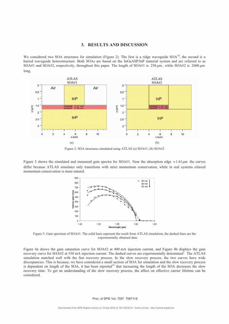
3. RESULTS AND DISCUSSION We considered two SOA structures for simulation (Figure 2). The first is a ridge waveguide SOA18, the second is a buried waveguide heterostructure. Both SOAs are based on the InGaASP/InP material system and are referred to as SOA#1 and SOA#2, respectively, throughout this paper. The length of SOA#1 is 258 �m , while SOA#2 is 2600 �m long.
(a) (b)
Figure 2: SOA structures simulated using ATLAS (a) SOA#1; (b) SOA#2
Figure 3 shows the simulated and measured gain spectra for SOA#1. Near the absorption edge �m61.1� the curves differ because ATLAS simulates only transitions with strict momentum conservation, while in real systems relaxed momentum conservation is more natural.
Figure 3: Gain spectrum of SOA#1. The solid lines represent the result from ATLAS simulation, the dashed lines are the
experimentally obtained data.
Figure 4a shows the gain saturation curve for SOA#2 at 400 mA injection current, and Figure 4b displays the gain recovery curve for SOA#2 at 550 mA injection current. The dashed curves are experimentally determined†. The ATLAS simulation matched well with the fast recovery process. In the slow recovery process, the two curves have wide discrepancies. This is because, we have considered a small section of SOA for simulation and the slow recovery process is dependent on length of the SOA, it has been reported19 that increasing the length of the SOA decreases the slow recovery time. To get an understanding of the slow recovery process, the affect on effective carrier lifetime can be considered.
Proc. of SPIE Vol. 7597 75971I-6
Downloaded from SPIE Digital Library on 12 Sep 2010 to 122.162.62.21. Terms of Use: http://spiedl.org/terms
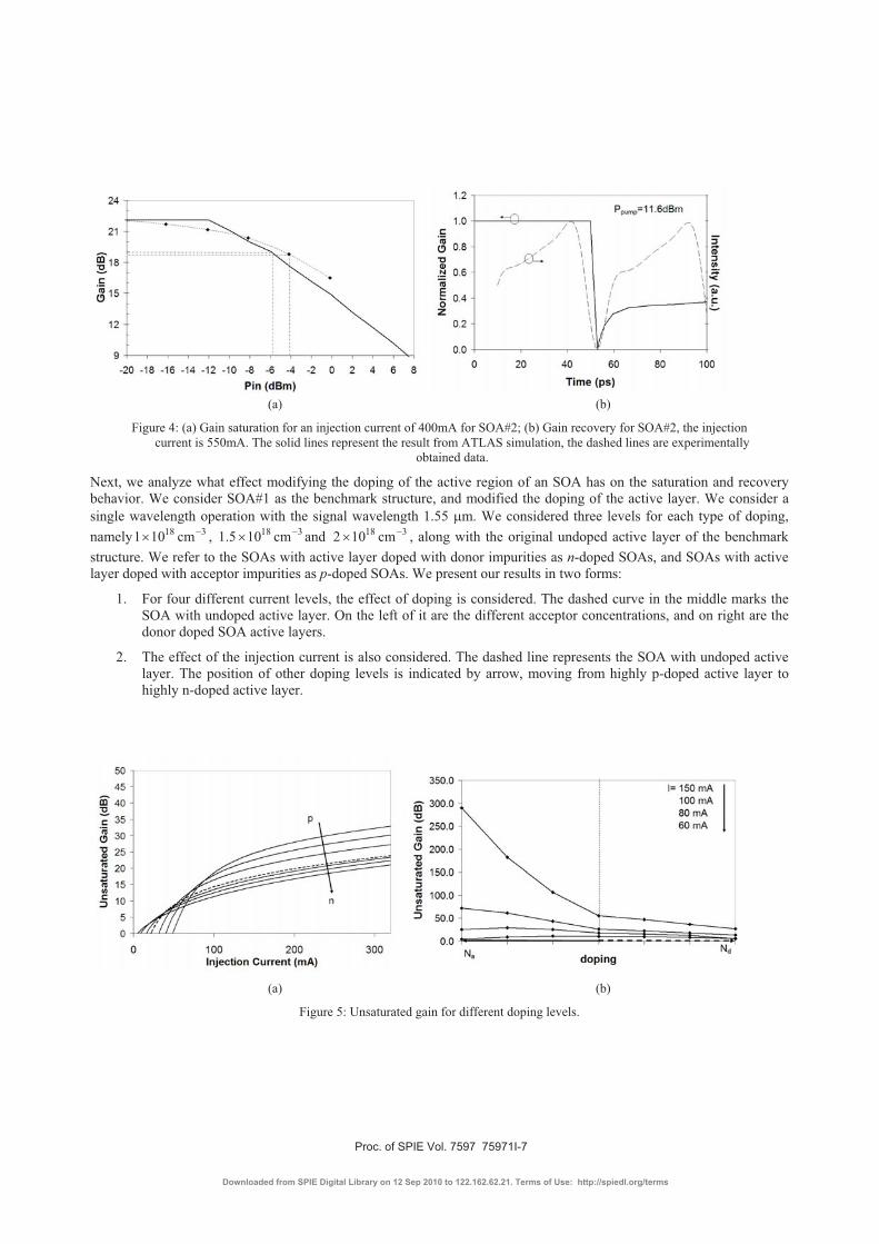
(a) (b)
Figure 4: (a) Gain saturation for an injection current of 400mA for SOA#2; (b) Gain recovery for SOA#2, the injection current is 550mA. The solid lines represent the result from ATLAS simulation, the dashed lines are experimentally
obtained data.
Next, we analyze what effect modifying the doping of the active region of an SOA has on the saturation and recovery behavior. We consider SOA#1 as the benchmark structure, and modified the doping of the active layer. We consider a single wavelength operation with the signal wavelength 1.55 �m. We considered three levels for each type of doping, namely 318 cm101 �� , 318 cm105.1 �� and 318 cm102 �� , along with the original undoped active layer of the benchmark structure. We refer to the SOAs with active layer doped with donor impurities as n-doped SOAs, and SOAs with active layer doped with acceptor impurities as p-doped SOAs. We present our results in two forms:
1. For four different current levels, the effect of doping is considered. The dashed curve in the middle marks the SOA with undoped active layer. On the left of it are the different acceptor concentrations, and on right are the donor doped SOA active layers.
2. The effect of the injection current is also considered. The dashed line represents the SOA with undoped active layer. The position of other doping levels is indicated by arrow, moving from highly p-doped active layer to highly n-doped active layer.
(a) (b)
Figure 5: Unsaturated gain for different doping levels.
Proc. of SPIE Vol. 7597 75971I-7
Downloaded from SPIE Digital Library on 12 Sep 2010 to 122.162.62.21. Terms of Use: http://spiedl.org/terms
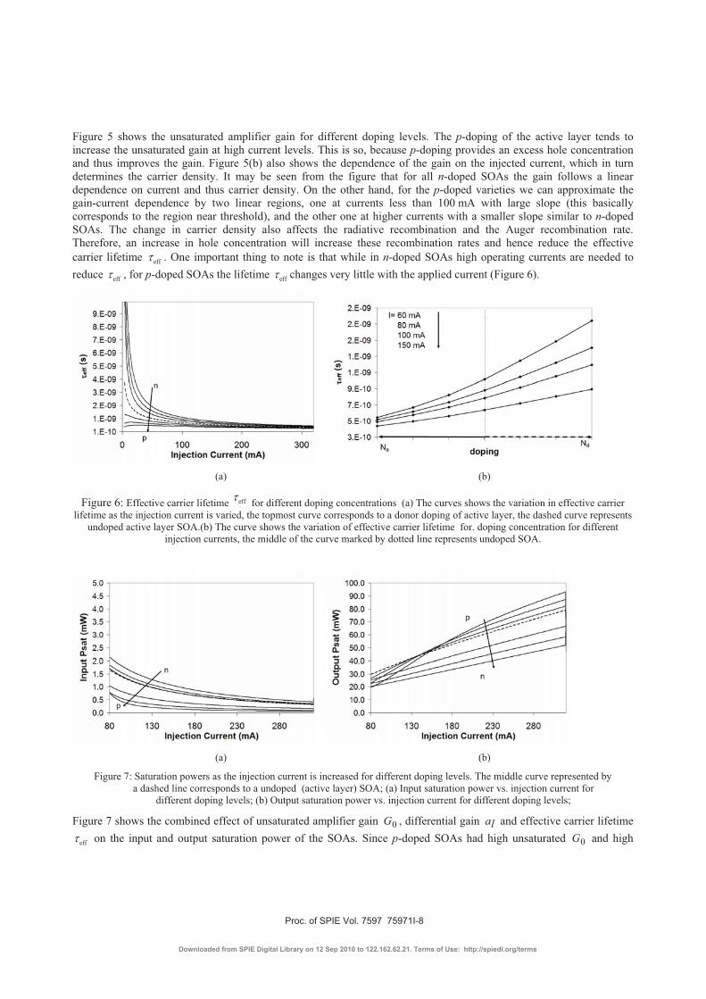
Figure 5 shows the unsaturated amplifier gain for different doping levels. The p-doping of the active layer tends to increase the unsaturated gain at high current levels. This is so, because p-doping provides an excess hole concentration and thus improves the gain. Figure 5(b) also shows the dependence of the gain on the injected current, which in turn determines the carrier density. It may be seen from the figure that for all n-doped SOAs the gain follows a linear dependence on current and thus carrier density. On the other hand, for the p-doped varieties we can approximate the gain-current dependence by two linear regions, one at currents less than 100 mA with large slope (this basically corresponds to the region near threshold), and the other one at higher currents with a smaller slope similar to n-doped SOAs. The change in carrier density also affects the radiative recombination and the Auger recombination rate. Therefore, an increase in hole concentration will increase these recombination rates and hence reduce the effective carrier lifetime eff� . One important thing to note is that while in n-doped SOAs high operating currents are needed to reduce eff� , for p-doped SOAs the lifetime eff� changes very little with the applied current (Figure 6).
(a) (b)
Figure 6: Effective carrier lifetime eff� for different doping concentrations (a) The curves shows the variation in effective carrier lifetime as the injection current is varied, the topmost curve corresponds to a donor doping of active layer, the dashed curve represents
undoped active layer SOA.(b) The curve shows the variation of effective carrier lifetime for. doping concentration for different injection currents, the middle of the curve marked by dotted line represents undoped SOA.
(a) (b)
Figure 7: Saturation powers as the injection current is increased for different doping levels. The middle curve represented by a dashed line corresponds to a undoped (active layer) SOA; (a) Input saturation power vs. injection current for
different doping levels; (b) Output saturation power vs. injection current for different doping levels;
Figure 7 shows the combined effect of unsaturated amplifier gain 0G , differential gain la and effective carrier lifetime
eff� on the input and output saturation power of the SOAs. Since p-doped SOAs had high unsaturated 0G and high
Proc. of SPIE Vol. 7597 75971I-8
Downloaded from SPIE Digital Library on 12 Sep 2010 to 122.162.62.21. Terms of Use: http://spiedl.org/terms
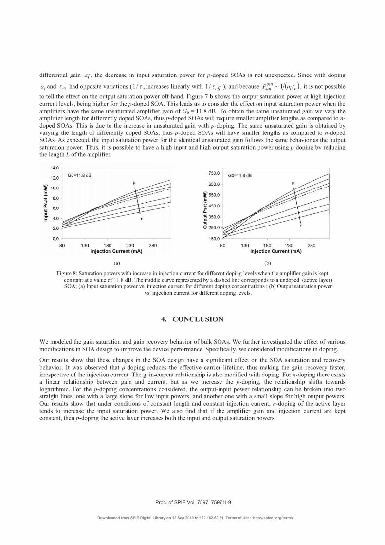
differential gain la , the decrease in input saturation power for p-doped SOAs is not unexpected. Since with doping
la and eff� had opposite variations ( e�/1 increases linearly with eff�/1 ), and because � eloutsat aP �1~ , it is not possible
to tell the effect on the output saturation power off-hand. Figure 7 b shows the output saturation power at high injection current levels, being higher for the p-doped SOA. This leads us to consider the effect on input saturation power when the amplifiers have the same unsaturated amplifier gain of G0 = 11.8 dB. To obtain the same unsaturated gain we vary the amplifier length for differently doped SOAs, thus p-doped SOAs will require smaller amplifier lengths as compared to n-doped SOAs. This is due to the increase in unsaturated gain with p-doping. The same unsaturated gain is obtained by varying the length of differently doped SOAs, thus p-doped SOAs will have smaller lengths as compared to n-doped SOAs. As expected, the input saturation power for the identical unsaturated gain follows the same behavior as the output saturation power. Thus, it is possible to have a high input and high output saturation power using p-doping by reducing the length L of the amplifier.
(a) (b)
Figure 8: Saturation powers with increase in injection current for different doping levels when the amplifier gain is kept constant at a value of 11.8 dB. The middle curve represented by a dashed line corresponds to a undoped (active layer) SOA; (a) Input saturation power vs. injection current for different doping concentrations ; (b) Output saturation power
vs. injection current for different doping levels.
4. CONCLUSION
We modeled the gain saturation and gain recovery behavior of bulk SOAs. We further investigated the effect of various modifications in SOA design to improve the device performance. Specifically, we considered modifications in doping.
Our results show that these changes in the SOA design have a significant effect on the SOA saturation and recovery behavior. It was observed that p-doping reduces the effective carrier lifetime, thus making the gain recovery faster, irrespective of the injection current. The gain-current relationship is also modified with doping. For n-doping there exists a linear relationship between gain and current, but as we increase the p-doping, the relationship shifts towards logarithmic. For the p-doping concentrations considered, the output-input power relationship can be broken into two straight lines, one with a large slope for low input powers, and another one with a small slope for high output powers. Our results show that under conditions of constant length and constant injection current, n-doping of the active layer tends to increase the input saturation power. We also find that if the amplifier gain and injection current are kept constant, then p-doping the active layer increases both the input and output saturation powers.
Proc. of SPIE Vol. 7597 75971I-9
Downloaded from SPIE Digital Library on 12 Sep 2010 to 122.162.62.21. Terms of Use: http://spiedl.org/terms
ACKNOWLEDGEMENT
Ms Amita Kapoor acknowledges DAAD ( Deutscher Akadmischer Austauschdienst) for providing the financial support to carry out the work in Germany at the Institute of Photonics and Quantum Electronics, Karlsruhe Institute of Technology, Germany. Enakshi K. Sharma also acknowledges DAAD for supporting the visit to the same Institute
REFERENCES
1. M J Connelly, “Semiconductor optical amplifiers”, Kluwer Academic Press, (2002). 2. M J Connelly, “Wideband semiconductor optical amplifier steady state numerical model”, IEEE J. Quantum
Electron., 37(3), 439-447 (2001). 3. J Mørk, M L Nielsen and T W Berg, “The dynamics of semiconductor optical amplifiers: modeling and
applications”, Opt. Photon. News, 14(7), 43-48 (2003). 4. P S Zory, “Quantum well lasers”, Academic Press, San Diego, California, (1993). 5. K Kahen, “Two dimensional simulation of laser diodes in the steady state”, IEEE Quantum Electron., 24(4), 641-
651 (1988). 6. D A Marcuse, “Computer model of an injection laser amplifier”, IEEE J. Quantum Electron., 9, 63-73 (1983). 7. P Brosson, “Analytic Model of a Semiconductor Optical Amplifier”, J. Lightw. Technol., 12, 49-54 (1994). 8. J Wang, A Maitra, C G Poulton, W Freude, and J Leuthold, “Temporal dynamics of the alpha factor in
semiconductor optical amplifiers”, J. Lightw. Technol., 25 (3), 12-14 (2007). 9. J L Pleumeekers, M Kauer, K Dreyer, C Burrus, A G Dentai, S Shunk, J Leuthold and C H Joyner, “Acceleration of
gain recovery in semiconductor optical amplifiers by optical injection Near Transparency Wavelength”, IEEE Photon. Technol. Lett., 14 (1), 12-14 (2002).
10. C B Su and V Lanzisera, “Effect of doping on the gain constant and modulation bandwidth of InGaAsP semiconductor lasers”, Appl. Phys. Lett., 45 (12), 1302-1304 (1984).
11. W Ng and Y Z Liu, “Effect of p-doping on carrier lifetime and threshold current density of 1-3 �m GaInAsP/InP lasers by liquid-phase epitaxy”, Electron. Lett., 16 (18), 693-695 (1980).
12. A Haug, “Influence of doping on threshold current of semiconductor lasers”, Electron. Lett., 21(18), 792-794 (1985).
13. O Qasaimeh, “Effect of doping on the optical characteristics of quantum-dot semiconductor optical amplifiers”, J. Lightw. Technol., 27(12), 1978-1984 (2009).
14. L Zhang, I Kang, A Bhardwaj, N Sauer, S Cabot, J Jaques, and D T Neilson, “Reduced recovery time semiconductor optical amplifier using p-type-doped multiple quantum wells”, IEEE Photon. Technol. Lett., 18(22), 2323-2325 (2006).
15. N K Dutta and Q Wang, “Semiconductor optical amplifier”, World Scientific (2006). 16. ATLAS user manual (2005) and (2006). 17. O Shulika, W Freude and J Leuthold, “Two dimensional simulation of semiconductor lasers and semiconductor
optical amplifiers using ATLAS”, OPT 2007, 34-38, (2007). 18. J Leuthold, “Advanced Indium-Phosphide waveguide Mach-Zehnder interferometer all-optical switches and
wavelength converters”, Dissertation, Zurich (1998). 19. F Girardin, G Guekos and A Houbavlis, “Gain recovery of bulk semiconductor optical amplifiers”, IEEE Photon.
Tech lett, 10 (6), 784-786 (1998). †The experiments were performed by Dipl.-Ing. Andrej Marculescu, Institute of Photonics and Quantum Electronics, Karlsruhe Institute of Technology, Germany.
Proc. of SPIE Vol. 7597 75971I-10
Downloaded from SPIE Digital Library on 12 Sep 2010 to 122.162.62.21. Terms of Use: http://spiedl.org/terms
Linear and Nonlinear Semiconductor Optical Amplifiers Wolfgang Freude, René Bonk, Thomas Vallaitis, Andrej Marculescu, Amita Kapoor1, Enakshi K. Sharma2,
Christian Meuer3, Dieter Bimberg3, Romain Brenot4, François Lelarge4, Guang-hua Duan4,Christian Koos, Juerg Leuthold
Institute of Photonics and Quantum Electronics, Karlsruhe Institute of Technology, 76131 Karlsruhe, Germany 1 On leave from Shaheed Rajguru College of Applied Sciences for Women, New Delhi, India
2 Department of Electronic Science, University of Delhi South Campus, New Delhi, India 3 Institute of Solid State Physics, TU Berlin, Germany
4 Alcatel-Thalès III-V Lab, Palaiseau, France Tel: +49 721 608-2492, Fax: +49 721 608-9098, e-mail: [email protected]
ABSTRACT Two selected applications of semiconductor optical amplifiers (SOA) are discussed, namely linear in-line ampli-fication in gigabit passive optical networks and fast nonlinear all-optical signal processing. We report on meas-urements demonstrating the suitability of quantum-dot (QD) and bulk SOA for the respective application areas. For in-line amplification the saturation power of the SOA should be large, while it has to be low for efficient signal processing. For bulk SOA we find by physically-based simulations that at large injection currents and for a fixed gain, p-doping (n-doping) of the active layer increases (decreases) the saturation power. Recently pub-lished experiments show that qualitatively these results carry over to QD-SOA. Keywords: Semiconductor optical amplifiers; Quantum-well, wire and dot devices; Semiconductor nonlinear optics
1. INTRODUCTIONSemiconductor optical amplifiers (SOA) attract attention mostly for two applications areas, namely for linear in-line amplification in gigabit passive optical networks (GPON), and for fast nonlinear all-optical signal process-ing. The respective application areas are determined by the SOA parameters injection current, gain, saturation power, recovery time, factor and noise figure. As opposed to bulk SOA, quantum-dot (QD) SOA are known for pattern-free amplification [1] and fast cross-gain modulation [2 4].
Here we show by experiments that QD-SOA are also well suited as linear in-line amplifiers [5 8] because of their large saturation power, wide dynamic range, large burst mode tolerance and small cross-phase modulation (XPM) due to a low -factor. On the other hand, bulk SOA usually have low saturation power and large -factor, which enables nonlinear signal processing via XPM as has been shown experimentally and theoretically [8 11]. However, from physically-based simulations we infer that a non-standard design, e. g., introducing an p-doping (n-doping) of the active layer, increases (decreases) the saturation power of bulk SOA for constant device length and current [12]. Previously, the effect of doping has been experimentally investigated for semiconductor lasers [13 15] and multiple quantum-well SOA [16]. For QD-SOA the influence of doping was theoretically studied [17] and experimentally evaluated very recently [18]. In the case of bulk SOA our physically-based modelling complements existing findings and gives deeper insight into the relevant mechanisms by separating the influences of modal cross-section, length, gain, differential gain and carrier lifetime.
2. PROPERTIES OF QUANTUM-DOT AND BULK SOA We classify QD-SOA and bulk SOA according to their gain linearity that is characterized by the input power
for a 3 dB gain compression [20], in terms of gain and phase recovery times, and by Henry’s -factor. Im-portant parameters are: Gain G = exp( g L), field confinement factor , material gain coefficient g a (N Nt), differential gain a, electron concentration N, transparency concentration Nt, longitudinal SOA extension 0 z L, unsaturated gain G0 and material gain constant g0, light frequency f = / (2 ), Planck’s constant h, modal cross-section A / , effective electron lifetime e, complex refractive index n = nr j ni for a time-space dependency exp[ j( t k0 (nr j ni)z] with ni < 0 for gain, free-space propagation constant k0 = / c,and vacuum speed of light c. The SOA output amplitude is in proportion to
satinP
exp jG and has a phase .Changes of phase and gain are denoted by and G, respectively. Then the following relations hold:
satin 0 0 0 0
0
/ /2 ln 2 / , 2 2 , exp , ,2 / / ln
r rr
e i
n N n N.A gP hf k G g L k n L a
G a n N g N G N
If the functions nr / N and ni / N have not the same time dependence, then the -factor will depend on time. Figure 1 shows typical plots of stationary and dynamical quantities for a QD-SOA at a wavelength of = 1.3 µm with a injection current of 500 mA (upper row) and for a bulk SOA at = 1.5 µm with an injection current of 100 mA (lower row). The QD-SOA of Fig. 1(left) exhibits a highly linear behaviour with a flat gain up to large input powers (large ), while the gain of a typical bulk SOA depends much stronger on the input power (small
).sat
inPsat
inP
ICTON 2010 We.D4.1
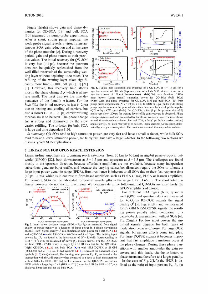
Figure 1(right) shows gain and phase dy-namics for QD-SOA [19] and bulk SOA [10] measured by pump-probe experiments. After a short, strong pump impulse, the weak probe signal reveals a virtually instan-taneous SOA gain reduction and an increase of the phase modulus | |. During a recovery period, gain and phase return to their previ-ous values. The initial recovery for QD-SOAis very fast (~ 1 ps), because the quantum dots can be quickly replenished from the well-filled reservoir of the surrounding wet-ting layer without depleting it too much. The refilling of the wetting layer takes signifi-cantly more time (~ 100 500 ps) [19] [21] [3]. However, this recovery time affects mostly the phase change , which is at any rate small. The inset displays the time de-pendence of the (small) -factor. For the bulk SOA the initial recovery is fast (~ 2 ps) due to heating and cooling of carriers, but also a slower (~ 10 100 ps) carrier refilling mechanism is to be seen. The phase change
is strong and dominated by the slow carrier refilling. The -factor for bulk SOA is large and time dependent [10].
Fig. 1. Typical gain saturation and dynamics of a QD-SOA at = 1.3 µm for a injection current of 500 mA (top row), and of a bulk SOA at = 1.5 µm for a injection current of 100 mA (bottom row). (left) Gain as a function of SOA input power. Large (small) saturation power for QD-SOA (bulk SOA)(right) Gain and phase dynamics for QD-SOA [19] and bulk SOA [10] frompump-probe experiments. At t = 10 ps, a 130 fs (QD) or 3 ps (bulk) wide strong pump impulse saturates the gain, which is then measured by a weak probe impulse (QD) or by a CW signal (bulk). For QD-SOA, a fast (1 ps for quantum dot refill) and a very slow (200 ps for wetting layer refill) gain recovery is observed. Phase changes are small and dominated by the slower recovery time. The inset shows a small time-dependent -factor. For bulk SOA, a fast (2 ps for hot carrier cooling) and a slow (50 ps) gain recovery is to be seen. Phase changes are large, domi-nated by a larger recovery time. The inset shows a small time-dependent -factor.
In summary: QD-SOA tend to high saturation power, are very fast and have a small -factor, while bulk SOA tend to have a lower saturation power, are fairly fast, but have a large -factor. In the following two sections we discuss typical SOA applications.
3. LINEAR SOA FOR GPON REACH EXTENSION Linear in-line amplifiers are promising reach extenders (from 20 km to 60 km) in gigabit passive optical net-works (GPON) [22], both downstream at = 1.5 µm and upstream at = 1.3 µm. The challenges are found mostly in the upstream direction, because affordable amplifiers are not available, because many independent subscribers generate burst traffic, and because the varying subscriber distances require the SOA to tolerate a large input power dynamic range (IPDR). Burst resilience is inherent to all SOA due to their fast response time (10 ps 1 ns), which is in contrast to fibre-based amplifiers such as EDFA (1 ms), PDFA or Raman amplifiers. Furthermore, SOA can be fabricated for central wavelengths in the range 1.25 1.65 µm. The short total dis-tances, however, do not ask for much gain. We demonstrate in the following that QD-SOA are most likely the
GPON amplifiers of choice.
Bulk-SOA
-30 -20 -10 0 1012
15
18
21 @ 1.3µm40 Gbit/s - RZ-OOK
9
12 For different SOA types (bulk, quantum well (QW) and quantum dot) we measured for 40 Gbit/s RZ-OOK signals the signal quality Q2 [5], Fig. 2(left), and we measured for 28 GBd NRZ-DQPSK signals the result-ing power penalty when comparing to a back-to-back measurement without SOA [6], Fig. 2(right). For low input powers the am-plified signals degrade for both types of modulation because of noise. For large OOK signals, bit pattern effects come into play. For large DQPSK signals it becomes impor-tant that fast amplitude transitions occur if the phase changes. During these phase tran-sitions with smaller amplitudes the gain re-covers, and this leads, via the -factor, to phase errors and therefore to a larger penalty.
In the case of Fig. 2(left) the IPDR is de-fined as the ratio of input powers Phi, Plo (at
QD-SOA
QW-SOA
-30 -20 -10 0 100
3
6
@ 1.5µm28Gb - NRZ- DQPSK
SOA Channel Input Power [dBm]
Pow
er P
ena
B]
Q2
[dB
]
SOA Channel Input Power [dBm]
lty [d QD-SOA
11 dB IPDRenhancement
5 dB IPDRenhancement
Fig. 2. Input power dynamic range (IPDR = Phi / Plo) as measured from signalquality or power penalty as a function of input power in a single wavelength channel. (left) Signal quality Q2 as a function of input power for a QD-SOA ( )and a QW-SOA ( ) with RZ-OOK at 40 Gbit/s and = 1.3 µm. The limiting inputpowers Phi , Plo are found at the intersection of Q2 = 15.6 dB (corresponding toBER = 10 9) with the measured Q2-curve [5], broken arrows. For the QD-SOA, we find IPDR = 27 dB, which is larger by a 11 dB than that for the QW-SOA.(right) QD-SOA ( , ) and bulk SOA ( , ) with NRZ-DQPSK at 28 Gbd(56 Gbit/s) and = 1.5 µm. Filled symbols ( , ) represent the I-channel, open symbols ( , ) the Q-channel. The limiting input powers Phi , Plo are found at the intersection with the 2 dB penalty when compared to a back-to-back measurement without SOA for BER = 10 3 [6], broken arrows. For the QD-SOA, we find an IPDR which is larger by a 5 dB (BER = 10 3) (larger by 6 dB for BER = 10 9, notdisplayed here) than that for the bulk SOA.
ICTON 2010 We.D4.1
2
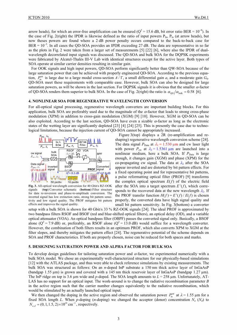
arrow heads), for which an error-free amplification can be ensured (Q2 = 15.6 dB, bit error ratio BER = 10 9). In the case of Fig. 2(right) the IPDR is likewise defined as the ratio of input powers Phi, Plo (at arrow heads), but now theses powers are found where a 2 dB power penalty occurs compared to the back-to-back case for BER = 10 3. In all cases the QD-SOA provides an IPDR exceeding 27 dB. The data are representative in so far as the plots in Fig. 2 were taken from a larger set of measurements [5] [22] [6], where also the IPDR of dual-wavelength decorrelated input signals was discussed. The QD-SOA and bulk SOA for the DQPSK experiments were fabricated by Alcatel-Thalès III-V Lab with identical structures except for the active layer. Both types of SOA operate at similar carrier densities resulting in similar gain.
For OOK signals and high input powers, QD-SOA perform significantly better than QW-SOA because of the large saturation power that can be achieved with properly engineered QD-SOA. According to the previous equa-tion, is large due to a large modal cross-section A / , a small differential gain a, and a moderate gain G0.QD-SOA meet these requirements with comparable ease. However, bulk SOA can also be designed for large saturation powers, as will be shown in the last section. For DQPSK signals it is obvious that the smaller -factor of QD-SOA renders them superior to bulk SOA. In the case of Fig. 2(right) the ratio is
satinP
QD bulk 0.58 [6].
4. NONLINEAR SOA FOR REGENERATIVE WAVELENGTH CONVERSION For all-optical signal processing, regenerative wavelength converters are important building blocks. For this application, bulk SOA are preferably used due to the magnitude of the -factor that leads to strong cross-phase modulation (XPM) in addition to cross-gain modulation (XGM) [9] [10]. However, XGM in QD-SOA can be also exploited. According to the last section, QD-SOA have even a sizable -factor as long as the electronic states of the wetting layer are significantly depleted [23] [4] [24] [25]. This is presently the case due to techno-logical limitations, because the injection current of QD-SOA cannot be appropriately increased.
Figure 3(top) displays a 2R (re-amplification and re-shaping) regenerative wavelength conversion scheme [24]. The data signal PData at 1 = 1.530 µm and cw laser light with power Pcw at 2 = 1.5361 µm are launched into a nonlinear medium, here a bulk SOA. If PData is large enough, it changes gain (XGM) and phase (XPM) for the co-propagating cw signal. The data at 2 after the SOA appear inverted and are distorted by bit pattern effects. For a fixed operating point and for representative bit patterns, a pulse reformatting optical filter (PROF) [9] transforms the complex optical spectrum E( f ) of the electric field after the SOA into a target spectrum E’( f ), which corre-sponds to the recovered data at the new wavelength 2. If the PROF transfer function H( f ) = E’( f ) / E( f ) is chosen properly, the converted data have high signal quality and small bit pattern sensitivity. In Fig. 3(bottom) a converter
setup with a bulk SOA is shown for 40 Gbit/s 33 % RZ-OOK signals [24]. The ideal PROF is approximated by two bandpass filters RSOF and BSOF (red and blue-shifted optical filters), an optical delay (OD), and a variable optical attenuator (VOA). An optical bandpass filter (OBPF) passes the converted signal only. Basically, a BSOF alone (Q2 = 7.9 dB) or, preferably, an RSOF alone (Q2 = 13.0 dB) would suffice for a wavelength converter. However, the combination of both filters results in an optimum PROF, which also converts XPM to XGM at the filter slopes, and thereby mitigates the pattern effect [24]. The regenerative potential of the scheme depends on SOA and PROF characteristics. If both are properly chosen, noise can be reduced for both spaces and marks.
5. DESIGNING SATURATION POWER AND ALPHA FACTOR FOR BULK SOA
To develop design guidelines for tailoring saturation power and -factor, we experimented numerically with a bulk SOA model. We chose an experimentally well-characterized structure for our physically-based simulations [12] with the ATLAS package, and thus were able to check reference simulations by existing measurements. The bulk SOA was structured as follows: On an n-doped InP substrate a 150 nm thick active layer of InGaAsP (bandgap 1.55 µm) is grown and covered with a 145 nm thick reservoir layer of InGaAsP (bandgap 1.27 µm). The InP ridge on top is 3.6 µm wide and p-doped. The SOA length amounts to L = 258 µm. Unfortunately, AT-LAS has no support for an optical input. The work-around is to change the radiative recombination parameter Bin the active region such that the carrier number changes equivalently to the radiative recombination, which would be stimulated by an actually launched optical input.
We then changed the doping in the active region and observed the saturation power at = 1.55 µm for a fixed SOA length L. When p-doping (n-doping) we changed the acceptor (donor) concentration Na (Nd) to
, respectively.
satinP
18 3, (0, 1, 1.5, 2) 10 cma dN
bulkSOA
Data signalPData , 1
cw signalPcw , 2
50:50
Invertedsignal
RSOF2 +
BSOF2
VOAODBPF
250:50 50:50
Convertedsignal
50 ps/div 10 ps/div
Q2=17.8 dBPROF
Q2= 8.3 dBQ2=19.8 dB
Fig. 3. All-optical wavelength conversion for 40 Gbit/s RZ-OOKsignals (top) Converter schematic (bottom) Filter structure for data re-inversion and phase-to-amplitude conversion. The inverted signal has low extinction ratio, strong bit pattern sensi-tivity and low signal quality. The PROF mitigates bit patterneffects and improves the signal quality.
ICTON 2010 We.D4.1
3
The resulting input saturation power is depicted in Fig. 4(left) as a function of the injection current while the un-saturated gain G0 varies. For a fixed current and p-doping (n-doping), the unsaturated modal gain g0 and the dif-ferential gain a increase (decrease)while the effective carrier lifetime edecreases (increases). These effects are the stronger the smaller the injection current becomes, and the resulting decreases (increases) accordingly. However, if the unsaturated gain G0 is kept constant and L changes with the injection current instead, then the product a e determines , Fig. 4(right). Assuming small injection currents (small N), and going from n to p-doping, the lifetime decreases, but the differential gain increases, so a e does not change so much. is then small and increases only little with p-doping. For large currents (large N),
is in general larger because of the reduced lifetime. However, when going from n to p-doping, e reduces (lifetime doping), while a remains virtually constant. Therefore a e becomes smaller, and the saturation power
increases. These tendencies also hold for QD-SOA [18].
satinP
satinP
satinP
satinP
satinP
Fig. 4. Input saturation power as a function of injection current with the dopant concen-tration as a parameter. (left) Constant length L and varying unsaturated gain G0(right) Constant unsaturated gain G0 and varying length L
For a linear amplifier with a given unsaturated gain G = 11.8 dB one should choose a large current of 250 mA together with p-doping that increases the gain constant, so that the length reduces to L = 100 µm. A large satura-tion power of results, which halves by the transition to n-doping. For a nonlinear amplifier with the same unsaturated gain, doping is not so important. A small current of 100 mA that decreases the gain con-stant and therefore needs a greater length of L = 280 µm reduces the saturation power to about .With p-doping, the -factor tends to reduce because of the larger gain constant and the smaller carrier concentra-tion that is required.
satin 10mWP
satin 3mWP
6. CONCLUSIONS For in-line amplification in future access networks, amplifiers with a large input power dynamic range are re-quired. These needs are best met by QD-SOA because of their small -factor. On the other hand, bulk SOA offer advantages as nonlinear network elements such as regenerative wavelength converters due their naturally larger
-factor. However, both types of SOA can be engineered for swapping their optimum application areas.
ACKNOWLEDGEMENT We acknowledge support by Karlsruhe Center for Functional Nanostructures (CFN), by Karlsruhe School of Optics & Photonics (KSOP), by EU project EURO-FOS, by Deutscher Akademischer Austauschdienst (DAAD), and by German Research Foundation (DFG) SFB 787.
REFERENCES [1] T. Akiyama et al., IEEE Photon. Technol. Lett., vol. 17, no. 8, pp. 1614–1616, Aug. 2005. [2] C. Meuer et al., Appl. Phys. Lett., vol. 93, no. 5, p. 051110, Aug. 2008. [3] C. Meuer et al., IEEE J. Sel. Topics Quantum Electron., vol. 15, pp. 749–756, May/June 2009. [4] S. Sygletos et al., J. Lightw. Technol., vol. 28, pp. 882–897, March 2010. [5] R. Bonk et al., Proc. ECOC'08, Sept 21–25, 2008, Brussels, Belgium. Paper Th.1.C.2. [6] R. Bonk et al., Proc. OFC'10, March 21–25, 2010, San Diego (CA), USA. Paper OThK3. [7] T. Vallaitis et al., Opt. Express, vol. 18, pp. 6270–6276, March 2010. [8] J. Leuthold et al., Proc. OFC'10, March 21–25, 2010, San Diego (CA), USA. Paper OThI3 [9] J. Leuthold et al., J. Lightw. Technol., vol. 22, 186 192, 2004. [10] J. Wang et al., J. Lightw. Technol., vol. 25, pp. 891–900, 2007. [11] J. Wang et al., Opt. Express, vol. 17, pp. 22639–22658, 2009. [12] A. Kapoor et al., Proc. SPIE, vol. 7597, 75971I, Feb. 2010. [13] C. B. Su et al., Appl. Phys. Lett., vol. 45, pp. 1302 1304, Dec. 1984. [14] W. Ng et al., Electron. Lett., vol. 16, pp. 693 695, Aug. 1980. [15] A. Haug, Electron. Lett., vol. 21, pp. 792 794, Aug. 1985. [16] L. Zhang et al., IEEE Photon. Technol. Lett., vol. 18, pp. 2323 2325, Nov. 2006. [17] O. Qasaimeh et al., J. Lightw. Technol., vol. 27, pp. 1978 1984, June 2009. [18] C. Meuer et al., IEEE Photon. J., vol. 2, pp. 141 151, April 2010. [19] T. Vallaitis et al., Opt. Express, vol. 16, pp. 170–178, Jan. 2008. [20] M. J. Connelly: Semiconductor optical amplifiers. New York: Kluwer Academic Press, 2004. Eq. (3.25) [21] J. Kim et al., Appl. Phys. Lett., vol. 94, pp. 041112-1 3, Jan. 2009. [22] R. Bonk et al., Proc. OFC'09, March 22–26, 2009, San Diego (CA), USA. Paper OWQ1 [23] R. Bonk et al., Proc. CLEO/IQEC’09, May 31–June 05, 2009, Baltimore (MD), USA. Paper CMC6 [24] J. Wang et.al., IEEE Photon. Technol. Lett., vol. 19, pp. 1955 1957, Dec. 2007. [25] G. Contestabile et al., Proc. OFC'10, March 21–25, 2010, San Diego (CA), USA. Paper OMT2
ICTON 2010 We.D4.1
4
Copyright © 2022 FDOKUMEN