Amplifiers and Oscillators | McGraw-Hill Education
156
11. Amplifiers and Oscillators 11.1. AMPLIFIER AND OSCILLATOR PRINCIPLES OF OPERATION 11.1.1. AMPLIFIERS: PRINCIPLES OF OPERATION 11.1.1.1. Gain In most amplifier applications the prime concern is gain. A generalized amplifier is shown in Fig. 11.1.1. The most widely applied definitions of gain using the quantities defined there are: 11.1.1.2. Bandwidth and Gain-Bandwidth Product Bandwidth is a measure of the range of frequencies within which an amplifier will respond. The frequency range (passband) is usually measured between the half-power (3-dB) points on the output-response-versus-frequency curve, for constant input. In some cases it is defined at the quarter-power points (6 dB). See Fig. 11.1.2. The gain-bandwidth product of a device is a commonly used figure of merit. It is defined for a bandpass amplifier as © McGraw-Hill Education. All rights reserved. Any use is subject to the Terms of Use, Privacy Notice and copyright information.
-
Upload
khangminh22 -
Category
Documents
-
view
0 -
download
0
Transcript of Amplifiers and Oscillators | McGraw-Hill Education

11. Amplifiers and Oscillators
11.1. AMPLIFIER AND OSCILLATOR PRINCIPLES OFOPERATION
11.1.1. AMPLIFIERS: PRINCIPLES OF OPERATION
11.1.1.1. Gain
In most amplifier applications the prime concern is gain. A generalized amplifier is shown in Fig. 11.1.1. The most widelyapplied definitions of gain using the quantities defined there are:
11.1.1.2. Bandwidth and Gain-Bandwidth Product
Bandwidth is a measure of the range of frequencies within which an amplifier will respond. The frequency range (passband) isusually measured between the half-power (3-dB) points on the output-response-versus-frequency curve, for constant input. Insome cases it is defined at the quarter-power points (6 dB). See Fig. 11.1.2.
The gain-bandwidth product of a device is a commonly used figure of merit. It is defined for a bandpass amplifier as
© McGraw-Hill Education. All rights reserved. Any use is subject to the Terms of Use, Privacy Notice and copyright information.

Figure 11.1.1 Input and output quantities of generalized amplifier.
where F = figure of merit (rad/s)
A = reference gain, either the maximum gain or the
gain at the frequency where the gain is purely
real or purely imaginary
B = 3-dB bandwidth (rad/s)
For low-pass amplifiers
where F = figure of merit (rad/s)
A = reference gain
W = upper cutoff frequency (rad/s)
In the case of vacuum tubes and certain other active devices this definition is reduced to
where F = figure of merit (rad/s)
g = transconductance of active device
C = total output capacitance, plus input capacitance of subsequent stage
11.1.1.3. Noise
The major types of noise are illustrated in Fig. 11.1.3. Important relations and definitions in noise computations are:
Noise factor
where S = signal power available at input
S = signal power available at output
N = noise power available at input at T = 290 K
N = noise power available at output
a
r
a
r
H
a
m
T
i
o
i
o
© McGraw-Hill Education. All rights reserved. Any use is subject to the Terms of Use, Privacy Notice and copyright information.

Available noise power
where the quantities are as defined in Fig. 11.1.3.
Excess noise factor
Figure 11.1.2 Amplifier response and bandwidth.
Figure 11.1.3 Noise-equivalent circuits.
where F − 1 = excess noise factor
N = total equivalent device noise referred to input
N = thermal noise of source at standard temperature
e
i
© McGraw-Hill Education. All rights reserved. Any use is subject to the Terms of Use, Privacy Notice and copyright information.

Noise temperature
where P is the average noise power available.
At a single input-output frequency in a two-port,
Effective input noise temperature
Noise Factor of Transmission Lines and Attenuators. The noise factor of two ports composed entirely of resistive elements atroom temperature (290 K) and an impedance matched loss of L = 1/G is F = L.
Cascaded noise factor
where F = overall noise factor
F = noise factor of first stage
F = noise factor of second stage
G = available gain of first stage
System Noise Temperature. Space probes and satellite communication systems using low-noise amplifiers and antennasdirected toward outer space make use of system noise temperatures. When we define T = antenna temperature, L =waveguide numeric loss (greater than 1), T = amplifier noise temperature, G = amplifier available gain, F = postamplifiernoise factor, and B = postamplifier bandwidth, this temperature can be calculated as
The quantity of interest is the output signal-to-noise ratio where S is available signal power at the antenna (assuming theantenna is matched to free space)
Generalized Noise Factor. A general representation of noise performances can be expressed in terms of Fig. 11.1.4. This is therepresentation of a noisy two-port in terms of external voltage and current noise sources with a correlation admittance. In thiscase the noise factor becomes
where F = noise factor
G = real part of Y
B = imaginary part of Y
G = conductance owing to the uncorrelated part of the noise current
Y = correlation admittance between cross product of current and voltage noise sources
G = real part of Y
B = imaginary part of Y
n ,av
A
T
1
2
A
A
E 1 A
A
s s
s s
u
γ
γ γ
γ γ
© McGraw-Hill Education. All rights reserved. Any use is subject to the Terms of Use, Privacy Notice and copyright information.
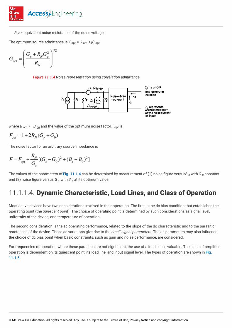
R = equivalent noise resistance of the noise voltage
The optimum source admittance is Y = G + jB
Figure 11.1.4 Noise representation using correlation admittance.
where B = −B and the value of the optimum noise factor F is
The noise factor for an arbitrary source impedance is
The values of the parameters of Fig. 11.1.4 can be determined by measurement of (1) noise figure versus B with G constantand (2) noise figure versus G with B at its optimum value.
11.1.1.4. Dynamic Characteristic, Load Lines, and Class of Operation
Most active devices have two considerations involved in their operation. The first is the dc bias condition that establishes theoperating point (the quiescent point). The choice of operating point is determined by such considerations as signal level,uniformity of the device, and temperature of operation.
The second consideration is the ac operating performance, related to the slope of the dc characteristic and to the parasiticreactances of the device. These ac variations give rise to the small-signal parameters. The ac parameters may also influencethe choice of dc bias point when basic constraints, such as gain and noise performance, are considered.
For frequencies of operation where these parasites are not significant, the use of a load line is valuable. The class of amplifieroperation is dependent on its quiescent point, its load line, and input signal level. The types of operation are shown in Fig.11.1.5.
11.1.1.5. Distortion
N
opt opt opt
opt gg opt
s s
s s
© McGraw-Hill Education. All rights reserved. Any use is subject to the Terms of Use, Privacy Notice and copyright information.

11.1.1.5. Distortion
Distortion takes many forms, most of them undesirable. The basic causes of distortion are nonlinearity in amplitude responseand nonuniformity of phase response. The most commonly encountered types of distortion are as follows:
Harmonic distortion is a result of nonlinearity in the amplitude transfer characteristics. The typical output contains not only thefundamental frequency but integer multiples of it.
Crossover distortion is a result of the nonlinear characteristics of a device when changing operating modes (e.g., in a push-pullamplifier). It occurs when one device is cut off and the second turned on if the crossover is not smooth between the twomodes.
Intermodulation distortion is a spurious output resulting from the mixing of two or more signals of different frequencies. Thespurious output occurs at the sum or difference of integer multiples of the original frequencies.
Cross-modulation distortion occurs when two signals pass through an amplifier and the modulation of one is transferred to theother.
Phase distortion results from the deviation from a constant slope of the output-phase–versus–frequency response of anamplifier. This deviation gives rise to echo responses in the output that precede and follow the main response, and a distortionof the output signal when an input signal having a large number of frequency components is applied.
11.1.1.6. Feedback Amplifiers
Feedback amplifiers fall into two categories: those having positive feedback (usually oscillators) and those having negativefeedback. The positive-feedback case is discussed under oscillators. The following discussion is concerned with negative-feedback amplifiers.
Figure 11.1.5 Classes of amplifier operation. Class S operation is a switching mode in which asquare-wave output is produced by a sine-wave input.
11.1.1.7. Negative Feedback
© McGraw-Hill Education. All rights reserved. Any use is subject to the Terms of Use, Privacy Notice and copyright information.

11.1.1.7. Negative Feedback
A simple representation of a feedback network is shown in Fig. 11.1.6. The closed-loop gain is given by
where A is the forward gain with feedback removed and B is the fraction of output returned to input.
Figure 11.1.6 Amplifier with feedback loop.
For negative feedback, A provides a 180° phase shift in mid-band, so that
in this frequencyrange
The quantity 1 − AB is called the feedback factor, and if the circuit is cut at any X point in Fig. 11.1.6, the open-loop gain is AB.
It can be shown that for large loop gain AB the closed-loop transfer function reduces to
The gain then becomes essentially independent of variations in A. In particular, if B is passive, the closed-loop gain is controlledonly by passive components. Feedback has no beneficial effect in reducing unwanted signals at the input of the amplifier, e.g.,input noise, but does reduce unwanted signals generated in the amplifier chain (e.g., output distortion).
The return ratio can be found if the circuit is opened at any point X (Fig. 11.1.6) and a unit signal P is injected at that X point.The return signal P′ is equal to the return ratio, since the input P is unity. In this case the return ratio T is the same at any point Xand is
The minus sign is chosen because the typical amplifier has an odd number of phase reversals and T is then a positive quantity.The return difference is by definition
It has been shown by Bode that
where Δ is the network determinant with XX point connected and Δ is the network determinant of amplifier when gain ofactive device is set to zero.
11.1.1.8. Stability
0
© McGraw-Hill Education. All rights reserved. Any use is subject to the Terms of Use, Privacy Notice and copyright information.
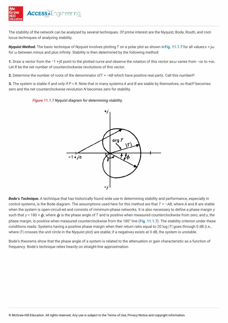
The stability of the network can be analyzed by several techniques. Of prime interest are the Nyquist, Bode, Routh, and root-locus techniques of analyzing stability.
Nyquist Method. The basic technique of Nyquist involves plotting T on a polar plot as shown in Fig. 11.1.7 for all values s = jωfor ω between minus and plus infinity. Stability is then determined by the following method:
1. Draw a vector from the −1 + j0 point to the plotted curve and observe the rotation of this vector as ω varies from −∞ to +∞.Let R be the net number of counterclockwise revolutions of this vector.
2. Determine the number of roots of the denominator of T = −AB which have positive real parts. Call this number P.
3. The system is stable if and only if P = R. Note that in many systems A and B are stable by themselves, so that P becomeszero and the net counterclockwise revolution N becomes zero for stability.
Figure 11.1.7 Nyquist diagram for determining stability.
Bode’s Technique. A technique that has historically found wide use in determining stability and performance, especially incontrol systems, is the Bode diagram. The assumptions used here for this method are that T = –AB, where A and B are stablewhen the system is open-circuit-ed and consists of minimum-phase networks. It is also necessary to define a phase margin γsuch that γ = 180 + , where is the phase angle of T and is positive when measured counterclockwise from zero, and γ, thephase margin, is positive when measured counterclockwise from the 180° line (Fig. 11.1.7). The stability criterion under theseconditions reads: Systems having a positive phase margin when their return ratio equal to 20 log |T| goes through 0 dB (i.e.,where |T| crosses the unit circle in the Nyquist plot) are stable; if a negative γ exists at 0 dB, the system is unstable.
Bode’s theorems show that the phase angle of a system is related to the attenuation or gain characteristic as a function offrequency. Bode’s technique relies heavily on straight-line approximation.
© McGraw-Hill Education. All rights reserved. Any use is subject to the Terms of Use, Privacy Notice and copyright information.

Figure 11.1.8 Equivalent circuits of active devices: (a) vacuum tube; (b) bipolar transistor; (c) field-effect transistor (FET).
Routh’s Criterion for Stability. Routh’s method has also been used to test the characteristic equations or return difference F = 1+ T = 0, to determine whether it has any roots that are real and positive or complex with positive real parts that will give rise togrowing exponential responses and hence instability.
Root-Locus Method. The root-locus method of analysis is a means of finding the variations of the poles of a closed-loopresponse as some network parameter is varied. The most convenient and commonly used parameter is that of the gain K. Thebasic equation then used is
This is a useful technique in feedback and control systems, but it has not found wide application in amplifier design. A detailedexposition of the technique is found in Truxal.
© McGraw-Hill Education. All rights reserved. Any use is subject to the Terms of Use, Privacy Notice and copyright information.

Figure 11.1.9 Definitions of active-network parameters: (a) general network; (b) ratios a i and b i ofincident and reflected waves (square root of power); (c) s parameters.
11.1.1.9. Active Devices Used in Amplifiers
There are numerous ways of representing active devices and their properties. Several common equivalent circuits are shown inFig. 11.1.8. Active devices are best analyzed in terms of the immittance or hybrid matrices. Figures 11.1.9 and 11.1.10 show thedefinition of the commonly used matrices, and their interconnections are shown in Fig. 11.1.11. The requirements at the bottomof Fig. 11.1.11 must be met before the interconnection of two matrices is allowed.
The matrix that is becoming increasingly important at higher frequencies is the S matrix. Here the network is embedded in atransmission-line structure, and the incident and reflected powers are measured and reflected coefficients and transmissioncoefficients are defined.
11.1.1.10. Cascaded and Distributed Amplifiers
© McGraw-Hill Education. All rights reserved. Any use is subject to the Terms of Use, Privacy Notice and copyright information.

11.1.1.10. Cascaded and Distributed Amplifiers
Most amplifiers are cascaded (i.e., connected to a second amplifier). The two techniques commonly used are shown in Fig.11.1.12. In the cascade structure the overall response is the product of the individual responses: in the distributed structure theresponse is one-half the sum of the individual responses, since each stage’s output is propagated in both directions. Incascaded amplifiers the frequency response and gain are determined by the active device as well as the interstage networks. Insimple audio amplifiers these interstage networks may become simple RC combinations, while in rf amplifiers they maybecome critically coupled double-tuned circuits. Interstage coupling networks are discussed in subsequent sections.
Figure 11.1.10 Network matrix terms.
In distributed structures (Fig. 11.1.12b), actual transmission lines are used for the input to the amplifier, while the output istaken at one end of the upper transmission line. The propagation time along the input line must be the same as that along theoutput line, or distortion will result. This type of amplifier, noted for its wide frequency response, is discussed later.
11.1.2. OSCILLATORS: PRINCIPLES OF OPERATION
11.1.2.1. Introduction
© McGraw-Hill Education. All rights reserved. Any use is subject to the Terms of Use, Privacy Notice and copyright information.

11.1.2.1. Introduction
An oscillator can be considered as a circuit that converts a dc input to a time-varying output. This discussion deals withoscillators whose output is sinusoidal, as opposed to the relaxation oscillator whose output exhibits abrupt transitions (seeSection 14). Oscillators often have a circuit element that can be varied to produce different frequencies.
An oscillator’s frequency is sensitive to the stability of the frequency-determining elements as well as the variation in the active-device parameters (e.g., effects of temperature, bias point, and aging). In many instances the oscillator is followed by a secondstage serving as a buffer, so that there is isolation between the oscillator and its load. The amplitude of the oscillation can becontrolled by automatic gain control (AGC) circuits, but the nonlinearity of the active element usually determines the amplitude.Variations in bias, temperature, and component aging have a direct effect on amplitude stability.
Figure 11.1.11 Matrix equivalents of network interconnections.
11.1.2.2. Requirements for Oscillation
Oscillators can be considered from two viewpoints: as using positive feedback around an amplifier or as a one-port network inwhich the real component of the input immittance is negative. An oscillator must have frequency-determining elements(generally passive components), an amplitude-limiting mechanism, and sufficient closed-loop gain to make up for the losses inthe circuit. It is possible to predict the operating frequency and conditions needed to produce oscillation from a Nyquist or Bodeanalysis. The prediction of output amplitude requires the use of nonlinear analysis.
11.1.2.3. Oscillator Circuits
Typical oscillator circuits applicable up to ultra high frequencies (UHF) are shown in Fig. 11.1.13. These are discussed in detailin the following subsections. Also of interest are crystal oscillators. In this case the crystal is used as the passive frequency-determining element. The frequency range of crystal oscillators extends from a few hundred hertz to over 200 MHz by use ofovertone crystals. The analysis of crystal oscillators is best done using the equivalent circuit of the crystal.
© McGraw-Hill Education. All rights reserved. Any use is subject to the Terms of Use, Privacy Notice and copyright information.

Figure 11.1.12 Multiamplifier structures: (a) cascade; (b) distributed.
Figure 11.1.13 Types of oscillators: (a) tuned-output; (b) Hartley; (c) phase-shift; (d) tuned-input; (e)Colpitts; (f) Wien bridge.
Figure 11.1.14 Phase-locked-loop oscillator.
Figure 11.1.15 Injection-locked oscillator.
11.1.2.4. Synchronization
© McGraw-Hill Education. All rights reserved. Any use is subject to the Terms of Use, Privacy Notice and copyright information.

11.1.2.4. Synchronization
Synchronization of oscillators is accomplished by using phase-locked loops or by direct low-level injection of a referencefrequency into the main oscillator. The diagram of a phase-locked loop is shown in Fig. 11.1.14 and that of an injection-lockedoscillator in Fig. 11.1.15.
11.1.2.5. Harmonic Content
The harmonic content of the oscillator output is related to the amount of oscillator output power at frequencies other than thefundamental. From the viewpoint of a negative-conductance (resistance) oscillator, better results are obtained if the curve ofthe negative conductance (or resistance) versus amplitude of oscillation is smooth and without an inflection point over theoperating range. Harmonic content is also reduced if the oscillator’s operating point Q is chosen so that the range of negativeconductance is symmetrical about Q on the negative conductance-versus-amplitude curve. This can be done by adjusting theoscillator’s bias point within the requirement of |G | = |G | for sustained oscillation (see Fig. 11.1.16).
11.1.2.6. Stability
The stability of the oscillator’s output amplitude and frequency from a negative-conductance viewpoint depends on thevariation of its negative conductance with operating point and the amount of fixed positive conductance in the oscillator’sassociated circuit. In particular, if the change of bias results in vertical translation of the conductance-(resistance)-versus-amplitude curve, the oscillator’s stability is related to the change of slope at the point where the circuit’s fixed conductanceintersects this curve (point Q in Fig. 11.1.16). If the |G | curve is of the shape of |G | , the oscillation can stop when a largeenough change in bias point occurs for |G | to be less than |G | for all amplitudes of oscillation. Stabilization of the amplitudeof oscillation may occur in the form of modifying G , G , or both to compensate for bias changes.
Particular types of oscillators and their parameters are discussed later in this section.
Figure 11.1.16 Device conductance vs. amplitude of oscillation.
11.2. AUDIO-FREQUENCY AMPLIFIERS AND OSCILLATORS
11.2.1. AUDIO-FREQUENCY AMPLIFIERS
Samuel M. Korzekwa
11.2.1.1. Preamplifiers
C D
D D 2
D C
C D
© McGraw-Hill Education. All rights reserved. Any use is subject to the Terms of Use, Privacy Notice and copyright information.

11.2.1.1. Preamplifiers
General Considerations. The function of a preamplifier is to amplify a low-level signal to a higher level before further processingor transmission to another location. The required amplification is achieved by increased signal voltage and/or impedancereduction. The amount of power amplification required varies with the particular application. A general guideline is to providesufficient preamplification to ensure that further signal handling adds minimal (or acceptable) signal-to-noise degradation.
Signal-to-Noise Considerations. The design of a preamplifier must consider all potential signal degradation from sources ofnoise, whether generated externally or within the preamplifier itself.
Examples of externally generated noise are hum and pickup, which may be introduced by the input-signal lines or the power-supply lines. Shielding of the input-signal lines often proves to be an acceptable solution. The preamplifier should be locatedclose to the transmitting source, and the preamplifier power gain must be sufficient to override interference that remains afterthese steps are taken.
A second major source of noise is that internally generated in the amplifier itself. The noise figure specified in decibels for apreamplifier, which serves as a figure of merit, is defined as the ratio of the available input-to-output signal-to-noise powerratios:
where F = noise figure of preamplifier
S = available signal input power
N = available noise input power
S = available signal output power
N = available noise output power
Design precautions to realize the lowest possible noise figure include the proper selection of the active device, optimum inputand output impedance, correct voltage and current biasing conditions, and pertinent design parameters of devices.
11.2.1.2. Low-Level Amplifiers
The low-level designation applies to amplifiers operated below maximum permissible power-dissipation, current, and voltagelimits. Thus many low-level amplifiers are purposely designed to realize specific attributes other than delivering the maximumattainable power to the load, such as gain stability, bandwidth, optimum noise figure, and low cost.
In an amplifier designed to be operated with a 24-V power supply and a specified load termination, for example, the operatingconditions may be such that the active devices are just within their allowable limits. If operated at these maximum limits, this isnot a low-level amplifier; however, if this amplifier also fulfills its performance requirements at a reduced power-supply voltageof 6 V, with resulting much lower internal dissipation levels, it becomes a low-level amplifier.
11.2.1.3. Medium-Level and Power Amplifiers
i
i
o
o
© McGraw-Hill Education. All rights reserved. Any use is subject to the Terms of Use, Privacy Notice and copyright information.

11.2.1.3. Medium-Level and Power Amplifiers
The medium-power designation for an amplifier implies that some active devices are operated near their maximum dissipationlimits, and precautions must be taken to protect these devices. If power-handling capability is taken as the criterion, the 5- to100-W power range is a current demarcation line. As higher-power-handling devices come into use, this range will tend to shiftto higher power levels.
The amount of power that can safely be handled by an amplifier is usually dictated by the dissipation limits of the activedevices in the output stages, the efficiency of the circuit, and the means used to extract heat to maintain devices within theirmaximum permissible temperature limits. The classes of operation (A, B, AB, C) are discussed relative to Fig. 11.1.5. Whensingle active devices do not suffice, multiple series or parallel configurations can be used to achieve higher voltage or poweroperation.
11.2.1.4. Multistage Amplifiers
An amplifier may take the form of a single stage or a complex single stage, or it may employ an interconnection of severalsteps. Various biasing, coupling, feedback, and other design alternatives influence the topology of the amplifier. For amultistage amplifier, the individual stages may be essentially identical or radically different. Feedback techniques may be usedat the individual stage level, at the amplifier functional level, or both, to realize bias stabilization, gain stabilization, output-impedance reduction, and so forth.
11.2.1.5. Typical Electron-Tube Amplifier
© McGraw-Hill Education. All rights reserved. Any use is subject to the Terms of Use, Privacy Notice and copyright information.

11.2.1.5. Typical Electron-Tube Amplifier
Figure 11.2.1 shows a typical electron-tube amplifier stage. For clarity the signal-source and load sections are shownpartitioned. For a multistage amplifier the source represents the equivalent signal generator of the preceding stage. Similarly,the load indicated includes the loading effect of the subsequent stage, if any.
The voltage gain from the grid of the tube to the output can be calculated to be
Similarly, the voltage gain from the source to the tube grid is
Combining the above equations gives the composite amplifier voltage gain
Figure 11.2.1 Typical triode electron-tube amplifier stage (biasing not shown).
This example illustrates the fundamentals of an electron-tube amplifier stage. Many excellent references treat this subject indetail.
11.2.1.6. Typical Transistor Amplifier
The analysis techniques used for electron-tube amplifier stages generally apply to transistorized amplifier stages. The principaldifference is that different active-device models are used.
The typical transistor stage shown in Fig. 11.2.2 illustrates a possible form of biasing and coupling. The source section ispartitioned and includes the preceding-stage equivalent generator, and the load includes subsequent stage-loading effects.Figure 11.2.3 shows the generalized h-equivalent circuit representation for transistors. Table 11.2.1 lists the h-parametertransformations for the common-base, common-emitter, and common-collector configurations.
© McGraw-Hill Education. All rights reserved. Any use is subject to the Terms of Use, Privacy Notice and copyright information.

Figure 11.2.2 Typical bipolar transistor-amplifier stage.
Figure 11.2.3 Equivalent circuit of transistor, based on h parameters.
Table 11.2.1 h Parameters of the Three Transistor Circuit Configurations
Common-base Common-emitter Common-collector
h h h (h + 1) h (h + 1)
h h h h (h + 1) − h 1
h h h – (h + 1)
h h h (h + 1) h (h + 1)
11 ib ib fe ib fe
12 rb ib ob fe rb
21 fb fe fe
22 ob ob fe ob fe
© McGraw-Hill Education. All rights reserved. Any use is subject to the Terms of Use, Privacy Notice and copyright information.

Figure 11.2.4 Simplified equivalent circuit of transistor amplifier stage.
While these parameters are complex and frequency-dependent, it is often feasible to use simplifications. Most transistors havetheir parameters specified by their manufacturers, but it may be necessary to determine additional parameters by test.
Figure 11.2.4 illustrates a simplified model of the transistor amplifier stage of Fig. 11.2.2. The common-emitter h parametersare used to represent the equivalent transistor. The voltage gain for this stage is
The complexity of analysis depends on the accuracy needed. Currently, most of the more complex analysis is performed withthe aid of computers. Several transistor-amplifier-analysis references treat this subject in detail.
11.2.1.7. Typical Multistage Transistor Amplifier
Figure 11.2.5 is an example of a capacitively coupled three-stage transistor amplifier. It has a broad frequency response,illustrating the fact that an audio amplifier can be useful in other applications. The component values are
Figure 11.2.5 Typical three-stage transistor amplifier.
This amplifier is designed to operate over a range of −55 to +125°C, with an output voltage swing of 2 V peak to peak andfrequency response down 3 dB at approximately 200 Hz and 2 MHz. The overall gain at 1000 Hz is nominally 88 dB at 25°C.
11.2.1.8. Biasing Methods
© McGraw-Hill Education. All rights reserved. Any use is subject to the Terms of Use, Privacy Notice and copyright information.

11.2.1.8. Biasing Methods
The biasing scheme used in an amplifier determines the ultimate performance that can be realized. Conversely, an amplifierwith poorly implemented biasing may suffer in performance, and be susceptible to catastrophic circuit failure owing to highstresses within the active devices. In view of the variation of parameters within the active devices, it is important that theamplifier function properly even when the initial and/or end-of-life parameters of the devices vary.
11.2.1.9. Electron-Tube Biasing
Biasing is intended to maintain the quiescent currents and voltages of the electron tube at the prescribed levels. The tube-platecharacteristics represent the biasing relations between the tube parameters.
The principal bias parameters (steady-state plate and grid voltages) can be readily identified by the construction of a load lineon the plate characteristic. The operating point Q is located at the intersection of the selected plate characteristic with the loadline.
11.2.1.10. Transistor Biasing
© McGraw-Hill Education. All rights reserved. Any use is subject to the Terms of Use, Privacy Notice and copyright information.

11.2.1.10. Transistor Biasing
Although the methods of biasing a transistor-amplifier stage are in many respects similar to those of an electron-tube amplifier,there are many different types of transistors, each characterized by different curves. Bipolar transistors are generallycharacterized by their collector and emitter families, while field-effect transistors have different characterizations. The npntransistor requires a positive base bias voltage and current (with respect to its emitter) for proper operation; the converse is truefor a pnp transistor.
Figure 11.2.6 Capacitively coupled npn transistor-amplifier stage.
Figure 11.2.6 illustrates a common biasing technique. A single power supply is used, and the transistor is self-biased with theunbypassed emitter resistor R . Although a graphical solution of the value of R could be found by referring to the collector-emitter curves, an iterative solution, described below, is also commonly used.
Because the performance of the transistors depends on the collector current and collector-to-emitter voltage, they are oftenselected as starting conditions for biasing design. The unbypassed emitter resistor R and collector resistor R , the primaryvoltage-gain-determining components, are determined next, taking into account other considerations such as the anticipatedmaximum signal level and available power supply V . The last step is to determine the R and R values.
11.2.1.11. Coupling Methods
Transformer coupling and capacitance coupling are commonly used in transistor and electron-tube audio amplifiers. Directcoupling is also used in transistor stages and particularly in integrated transistor amplifiers. Capacitance coupling, referred toas RC coupling, is the most common method of coupling stages of an audio amplifier. The discrete-component transistorizedamplifier stage shown in Fig. 11.2.6 serves as an example of RC coupling, where C and C are the input and output couplingcapacitors, respectively.
e e
e c
cc 1 2
i o
© McGraw-Hill Education. All rights reserved. Any use is subject to the Terms of Use, Privacy Notice and copyright information.
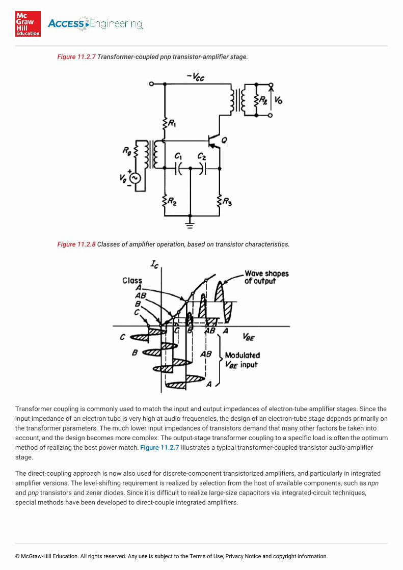
Figure 11.2.7 Transformer-coupled pnp transistor-amplifier stage.
Figure 11.2.8 Classes of amplifier operation, based on transistor characteristics.
Transformer coupling is commonly used to match the input and output impedances of electron-tube amplifier stages. Since theinput impedance of an electron tube is very high at audio frequencies, the design of an electron-tube stage depends primarily onthe transformer parameters. The much lower input impedances of transistors demand that many other factors be taken intoaccount, and the design becomes more complex. The output-stage transformer coupling to a specific load is often the optimummethod of realizing the best power match. Figure 11.2.7 illustrates a typical transformer-coupled transistor audio-amplifierstage.
The direct-coupling approach is now also used for discrete-component transistorized amplifiers, and particularly in integratedamplifier versions. The level-shifting requirement is realized by selection from the host of available components, such as npnand pnp transistors and zener diodes. Since it is difficult to realize large-size capacitors via integrated-circuit techniques,special methods have been developed to direct-couple integrated amplifiers.
11.2.1.12. Classes A, B, AB, and C Operation
© McGraw-Hill Education. All rights reserved. Any use is subject to the Terms of Use, Privacy Notice and copyright information.

11.2.1.12. Classes A, B, AB, and C Operation
The output or power stage of an amplifier is usually classified as operating class A, B, AB, or C, depending on the conductioncharacteristics of the active devices (see Fig. 11.1.5). These definitions can also apply to any intermediate amplifier stage.Figure 11.2.8 illustrates relations between the class of operation and conduction using transistor parameters. This figure wouldbe essentially the same for an electron-tube amplifier with the tube plate current and grid voltage as the equivalent deviceparameters.
Subscripts may be used to denote additional conduction characteristics of the device. For example, the electron-tube gridconduction can also be further classified as A , to show that no grid current flows, or A , to show that grid-current conductionexists during some portion of the cycle.
11.2.1.13. Push-Pull Amplifiers
In a single-ended amplifier the active devices conduct continuously. The single-ended configuration is generally used in low-power applications, operated in class A. For example, preamplifiers and low-level amplifiers are generally operated single-ended, unless the output power levels necessitate the more efficient power handling of the push-pull circuit.
In a push-pull configuration there are at least two active devices that alternately amplify the negative and positive cycles of theinput waveform. The output connection to the load is most often transformer-coupled. An example of a transformer input andoutput in a push-pull amplifier is illustrated in Fig. 11.2.9. Direct-coupled push-pull amplifiers and capacitively coupled push-pullamplifiers are also feasible, as illustrated in Fig. 11.2.10.
Figure 11.2.9 Transformer-coupled push-pull transistor stage.
The active devices in push-pull are usually operated either in class B or AB because of the high power-conversion efficiency.Feedback techniques can be used to stabilize gain, stabilize biasing or operating points, minimize distortion, and the like.
11.2.1.14. Output Amplifiers
The function of an audio output amplifier is to interface with the preceding amplifier stages and to provide the necessary driveto the load. Thus the output-amplifier designation does not uniquely identify a particular amplifier class. When several differenttypes of amplifiers are cascaded between the signal source and its load, e.g., a high-power speaker, the last-stage amplifier isdesignated as the output amplifier. Because of the high power requirements, this amplifier is usually a push-pull type operatingeither in class B or AB.
11.2.1.15. Stereo Amplifiers
1 2
© McGraw-Hill Education. All rights reserved. Any use is subject to the Terms of Use, Privacy Notice and copyright information.

11.2.1.15. Stereo Amplifiers
A stereo amplifier provides two separate audio channels properly phased with respect to each other. The objective of this two-channel technique is to enhance the audio reproduction process, making it more realistic and lifelike. It is also feasible toextend the system to contain more than two channels of information. A stereo amplifier is a complete system that contains itspower supply and other commonly required control functions.
Figure 11.2.10 (a) Direct- and (b) capacitively coupled push-pull stages.
Each channel has its own preamplifier, medium-level stages, and output power stage, with different gain and frequencyresponses for each mode of operation, e.g., for tape, phonograph, CD, and so forth. The input signal is selected from thephonograph input connection, tape input, or a turner output. Special-purpose trims and controls are also used to optimizeperformance on each mode. The bandwidth of the amplifier extends to 20 kHz or higher.
11.2.2. AUDIO OSCILLATORS
Robert J. McFadyen
11.2.2.1. General Considerations
In the strict sense, an audio oscillator is limited to frequencies from about 15 to 20,000 Hz, but a much wider frequency range isincluded in most oscillators used in audio measurements since knowledge of amplifier characteristics in the region aboveaudibility is often required.
For the production of sinusoidal waves, audio oscillators consist of an amplifier having a nonlinear power gain characteristic,with a path for regenerative feedback. Single- and multistage transistor amplifiers with LC or RC feedback networks are mostoften used. The term harmonic oscillator is used for these types. Relaxation oscillators, which may be designed to oscillate inthe audio range, exhibit sharp transitions in the output voltages and currents. Relaxation oscillators are treated in Section 14.
The instantaneous excursions of the operating point in a harmonic oscillator is restricted to the range where the circuit exhibitsan impedance with a negative real part. The amplifier supplies the power, which is dissipated in the feedback path and the load.The regenerative feedback would cause the amplitude of oscillation to grow without bound were it not for the fact that thedynamic range of the amplifier is limited by circuit nonlinearities. Thus, in most sine-wave audio oscillators; the operatingfrequency is determined by passive-feedback elements, whereas the amplitude is controlled by the active-circuit design.
© McGraw-Hill Education. All rights reserved. Any use is subject to the Terms of Use, Privacy Notice and copyright information.

Analytical expressions predicting the frequency and required starting conditions for oscillation can be derived using Bode’samplifier feedback theory, and the stability theorem of Nyquist. Since this analytical approach is based on a linear-circuit model,the results are approximate but usually suitable for design of sinusoidal oscillators. No prediction on waveform amplituderesults, since this is determined by nonlinear-circuit characteristics. Estimates of the waveform amplitude can be made fromthe bias and limiting levels of the active circuits. Separate limiters and AGC techniques are also useful for controlling theamplitude to a prescribed level. Graphical and nonlinear analysis methods can also be used for obtaining a prediction of theamplitude of oscillation.
A general formulation suitable for a linear analysis of almost all audio oscillators can be derived from the feedback diagram inFig. 11.2.11. Note that the amplifier internal feedback generator has been neglected: that is, y is assumed to be zero. Thisassumption of unilateral amplification is almost always valid in the audio range even for single-stage transistor amplifiers.
The stability requirements for the circuit are derived from the closed-loop-gain expression
(1)
where the gain A is treated as a negative quantity for an inverting amplifier. Infinite closed-loop gain occurs when AB is equal tounity, and this defines the oscillatory condition. In terms of the equivalent circuit parameters used in Fig. 11.2.1,
(2)
Figure 11.2.11 Oscillator representations: (a) generalized feedback circuit; (b) equivalent y-parameter circuit.
In the audio range, y remains real, but the fractional portion of the function is complex because β is frequency-sensitive.Therefore, the open-loop gain Aβ can be expressed in the general form
(3)
It follows from Nyquist’s stability theorem that this feedback system will be unstable if, first, the phase shift of Aβ is zero and,second, the magnitude is equal to or greater than unity. Applying this criterion to Eq. (3) yields the following two conditions foroscillation:
(4) (5)
12A
21A
© McGraw-Hill Education. All rights reserved. Any use is subject to the Terms of Use, Privacy Notice and copyright information.

Equation (4) results from the phase condition and determines the frequency of oscillation. The inequality in Eq. (5) is theconsequence of the magnitude constraint and defines the necessary condition for sustained oscillation. Equation (5) isevaluated at the oscillation frequency determined from Eq. (4).
A large number of single-stage oscillators have been developed in both vacuum-tube and transistor versions. The transistorcircuits followed by direct analogy from the earlier vacuum-tube circuits. In the following examples, transistor versions areillustrated, but the y-parameter equations apply to other devices as well.
11.2.2.2. LCOscillators
The Hartley oscillator circuit is one of the oldest forms: the transistor version is shown in Fig. 11.2.12. With the collector andbase at opposite ends of the tuned circuit, the 180° phase relation is secured, and feedback occurs through mutual inductancebetween the two parts of the coil. The frequency and condition for oscillation are expressed in terms of the transistor yparameters and feedback inductance L, inductor coupling coefficient k, inductance ratio n, and tuning capacitance C. Thefrequency of oscillation is
Figure 11.2.12 Hartley oscillator circuit.
Figure 11.2.13 Colpitts oscillator circuit.
The condition for oscillation is
© McGraw-Hill Education. All rights reserved. Any use is subject to the Terms of Use, Privacy Notice and copyright information.

The admittance parameters of the bias network R , R , and R , as well as the reactance of bypass capacitor C and couplingcapacitor C , have been neglected. These admittances could be included in the amplifier y parameters in cases where theireffect is not negligible.
If
(6)
the frequency of oscillation will be essentially independent of transistor parameters.
The transistor version of the Colpitts oscillator is shown in Fig. 11.2.13. Capacitors C and nC in combination with inductance Ldetermine the resonant frequency of the circuit. A fraction of the current flowing in the tank circuit is regeneratively fed back tothe base through the coupling capacitor C . Bias resistors R , R , R , and R , as well as capacitors C and C , are chosen soas not to affect the frequency or conditions for oscillation. The frequency of oscillation is
The condition for oscillation is
Alternatively, the bias element admittances may be included in the amplifier y parameters.
In the Colpitts circuit, if the ratio of C/L is chosen so that
(7)
the frequency of oscillation is essentially determined by the tuned-circuit parameters.
Figure 11.2.14 Tuned-collector oscillator.
1 2 3
2
2 1 2 3 L 1 2
© McGraw-Hill Education. All rights reserved. Any use is subject to the Terms of Use, Privacy Notice and copyright information.

Figure 11.2.15 RC oscillator with high-pass feedback network.
Another oscillator configuration useful in the audio-frequency range is the tuned-collector circuit shown in Fig. 11.2.14. Hereregenerative feedback is furnished via the transformer turns ratio N from the collector to base. The frequency of oscillation is
The condition for oscillation is
If the ratio of C/L is such that
(8)
the frequency of oscillation is specified by ω = 1/LC. This circuit can be tuned over a wide range by varying the capacitor C andis compatible with simple biasing techniques.
11.2.2.3. RC Oscillators
2
© McGraw-Hill Education. All rights reserved. Any use is subject to the Terms of Use, Privacy Notice and copyright information.

11.2.2.3. RC Oscillators
Audio sinusoidal oscillators can be designed using an RC ladder network (of three or more sections) as a feedback path in anamplifier. This scheme originally appeared in vacuum-tube circuits, but the principles have been directly extended to transistordesign. RC phase-shift oscillators can be distinguished from tuned oscillators in that the feedback network has a relativelybroad frequency-response characteristic.
Typically, the phase-shift network has three RC sections of either a high- or a low-pass nature. Oscillation occurs at thefrequency where the total phase shift is 180° when used with an inverting amplifier. Figures 11.2.15 and 11.2.16 showexamples of high-pass and low-pass feedback-connection schemes. The amplifier is a differential pair with a transistor currentsource, a configuration which is common in integrated-circuit amplifiers. The output is obtained at the opposite collector fromthe feedback connection, since this minimizes external loading on the phase-shift network. The conditions for, and thefrequency of, oscillation are derived, assuming that the input resistance of the amplifier, which loads the phase-shift network,has been adjusted to equal the resistance R. The load resistor R is considered to be part of the amplifier output resistance, andit is included in y . The frequency of oscillation for the high-pass case is
The condition for oscillation for the high-pass case is
The frequency of oscillation for the low-pass case is
The condition for oscillation for the low-pass case is
11.2.2.4. Null-Network Oscillators
In almost all respects null-network oscillators are superior to the RC phase-shift circuits described in the previous paragraph.While many null-network configurations are useful (including the bridged-T and twin-T), the Wien bridge design predominates.
The general form for the Wien bridge oscillator is shown in Fig. 11.2.17. In the figure, an ideal differential voltage amplifier isassumed, i.e., one with infinite input impedance and zero output impedance.
L
22A
© McGraw-Hill Education. All rights reserved. Any use is subject to the Terms of Use, Privacy Notice and copyright information.
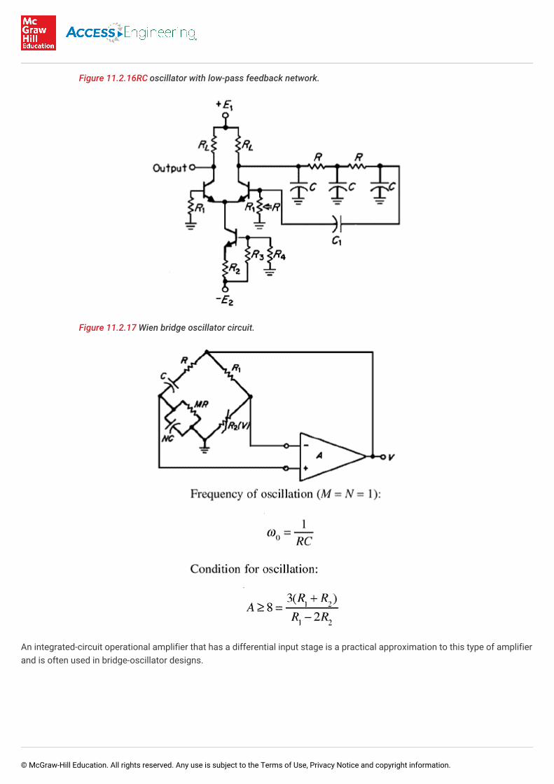
Figure 11.2.16RC oscillator with low-pass feedback network.
Figure 11.2.17 Wien bridge oscillator circuit.
An integrated-circuit operational amplifier that has a differential input stage is a practical approximation to this type of amplifierand is often used in bridge-oscillator designs.
© McGraw-Hill Education. All rights reserved. Any use is subject to the Terms of Use, Privacy Notice and copyright information.

The Wien bridge is used as the feedback network, with positive feedback provided through the RC branches for regenerationand negative feedback through the resistor divider. Usually the resistor-divider network includes an amplitude-sensitive devicein one or both arms which provides automatic correction for variation of the amplifier gain. Circuit elements such as a tungstenlamp, thermistor, and field-effect transistor used as the voltage-sensitive resistance element maintain a constant output levelwith a high degree of stability. Amplitude variations of less than ±1 percent over the band from 10 to 100,000 Hz are realizable.In addition, since the amplifier is never driven into the nonlinear region, harmonic distortion in the output waveform isminimized. For the connection shown in Fig. 11.2.17, an increase in V will cause a decrease in R , restoring V to the originallevel.
The lamp or thermistor have thermal time constants that set at a lower frequency limit on this method of amplitude control.When the period is comparable with the thermal time constant, the change in resistance over an individual cycle distorts theoutput waveform. There is an additional degree of freedom with the field-effect transistor, since the control voltage must bederived by a separate detector from the amplifier output. The time constant of the detector, and hence the resistor, are set by acapacitor, which can be chosen commensurate with the lowest oscillation frequency desired.
At ω the positive feedback predominates, but at harmonics of ω the net negative feedback reduces the distortioncomponents. Typically, the output waveform exhibits less than 1 percent total harmonic distortion. Distortion components wellbelow 0.1 percent in the mid-audio-frequency range are also achieved.
Unlike LC oscillators, in which the frequency is inversely proportional to the square root of L and C, in the Wien bridge ω variesas 1/RC. Thus, a tuning range in excess of 10:1 is easily achieved. Continuous tuning within one decade is usuallyaccomplished by varying both capacitors in the reactive feedback branch. Decade changes are normally accomplished byswitching both resistors in the resistive arm. Component tracking problems are eased when the resistors and capacitors arechosen to be equal.
Almost any three-terminal null network can be used for the reactive branch in the bridge; the resistor divider network adjusts thedegree of imbalance in the manner described. Many of these networks lack the simplicity of the Wien bridge since they mayrequire the tracking of three components for frequency tuning. For this reason networks such as the bridged-T and twin-T areusually restricted to fixed-tuned applications.
11.2.2.5. Low-Frequency Crystal Oscillators
Quartz-crystal resonators are used where frequency stability is a primary concern. The frequency variations with both time andtemperature are several orders of magnitude lower than obtainable in LC or RC oscillator circuits. The very high stiffness andelasticity of piezoelectric quartz make it possible to produce resonators extending from approximately 1 kHz to 200 MHz. Theperformance characteristics of crystal depend on both the particular cut and the mode of vibration (see Section 5). Forconvenience, each “cut-mode” combination is considered as a separate piezoelectric element, and the more commonly usedelements have been designated with letter symbols. The audio-frequency range (above 1 kHz) is covered by elements J, H, N,and XY, as shown in Table 11.2.2.
The temperature coefficients vary with frequency, i.e., with the crystal dimensions, and except for the H element, a parabolicfrequency variation with temperature is observed. The H element is characterized by a negative temperature coefficient on theorder of –10 ppm/°C. The other elements have lower temperature coefficients, which at some temperatures are zero becauseof the parabolic nature of the frequency-deviation curve. The point where the zero temperature coefficient occurs is adjustableand varies with frequency. At temperatures below this point the coefficient is positive, and at higher temperatures it is negative.On the slope of the curves the temperature coefficients for the N and XY elements are on the order of 2 ppm/°C, whereas the Jelement is about double at 4 ppm/°C.
2
0 0
0
© McGraw-Hill Education. All rights reserved. Any use is subject to the Terms of Use, Privacy Notice and copyright information.
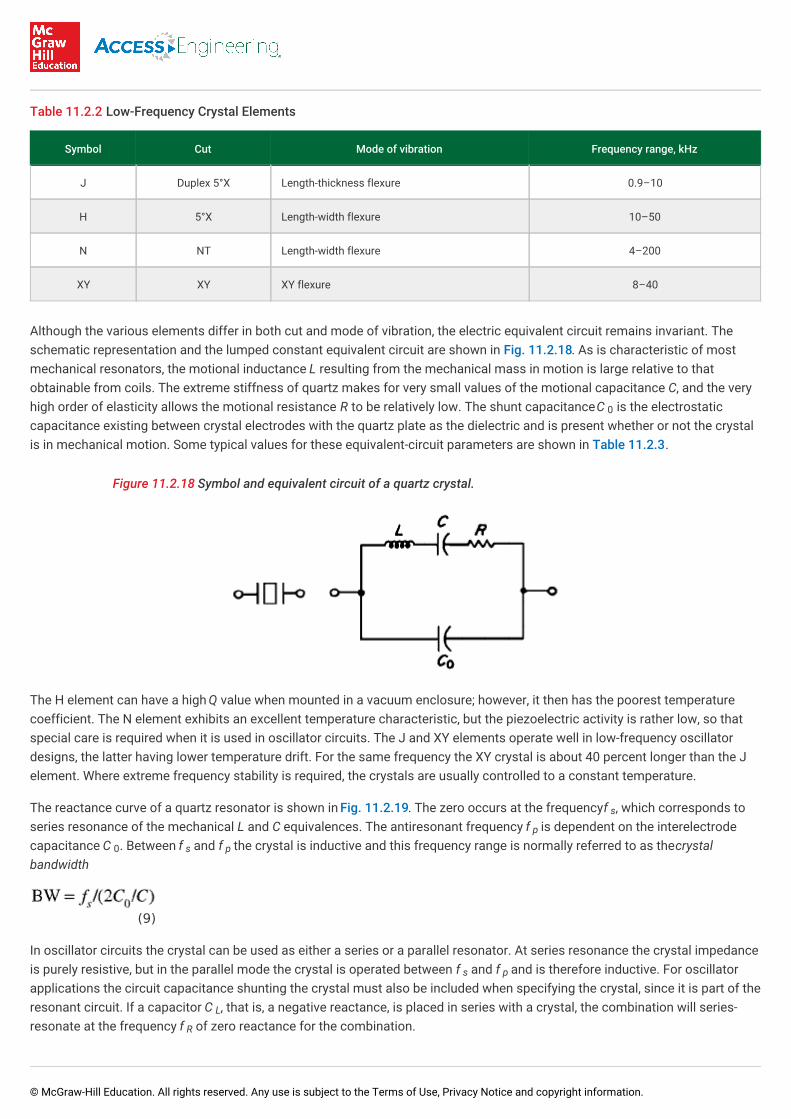
Table 11.2.2 Low-Frequency Crystal Elements
Symbol Cut Mode of vibration Frequency range, kHz
J Duplex 5°X Length-thickness flexure 0.9–10
H 5°X Length-width flexure 10–50
N NT Length-width flexure 4–200
XY XY XY flexure 8–40
Although the various elements differ in both cut and mode of vibration, the electric equivalent circuit remains invariant. Theschematic representation and the lumped constant equivalent circuit are shown in Fig. 11.2.18. As is characteristic of mostmechanical resonators, the motional inductance L resulting from the mechanical mass in motion is large relative to thatobtainable from coils. The extreme stiffness of quartz makes for very small values of the motional capacitance C, and the veryhigh order of elasticity allows the motional resistance R to be relatively low. The shunt capacitance C is the electrostaticcapacitance existing between crystal electrodes with the quartz plate as the dielectric and is present whether or not the crystalis in mechanical motion. Some typical values for these equivalent-circuit parameters are shown in Table 11.2.3.
Figure 11.2.18 Symbol and equivalent circuit of a quartz crystal.
The H element can have a high Q value when mounted in a vacuum enclosure; however, it then has the poorest temperaturecoefficient. The N element exhibits an excellent temperature characteristic, but the piezoelectric activity is rather low, so thatspecial care is required when it is used in oscillator circuits. The J and XY elements operate well in low-frequency oscillatordesigns, the latter having lower temperature drift. For the same frequency the XY crystal is about 40 percent longer than the Jelement. Where extreme frequency stability is required, the crystals are usually controlled to a constant temperature.
The reactance curve of a quartz resonator is shown in Fig. 11.2.19. The zero occurs at the frequency f , which corresponds toseries resonance of the mechanical L and C equivalences. The antiresonant frequency f is dependent on the interelectrodecapacitance C . Between f and f the crystal is inductive and this frequency range is normally referred to as the crystalbandwidth
(9)
In oscillator circuits the crystal can be used as either a series or a parallel resonator. At series resonance the crystal impedanceis purely resistive, but in the parallel mode the crystal is operated between f and f and is therefore inductive. For oscillatorapplications the circuit capacitance shunting the crystal must also be included when specifying the crystal, since it is part of theresonant circuit. If a capacitor C , that is, a negative reactance, is placed in series with a crystal, the combination will series-resonate at the frequency f of zero reactance for the combination.
0
s
p
0 s p
s p
L
R
© McGraw-Hill Education. All rights reserved. Any use is subject to the Terms of Use, Privacy Notice and copyright information.
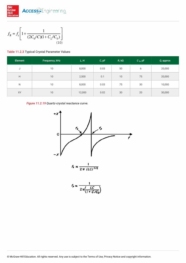
(10)
Table 11.2.3 Typical Crystal Parameter Values
Element Frequency, kHz L, H C, pF R, kΩ C , pF Q, approx
J 10 8,000 0.03 50 6 20,000
H 10 2,500 0.1 10 75 20,000
N 10 8,000 0.03 75 30 10,000
XY 10 12,000 0.02 30 20 30,000
Figure 11.2.19 Quartz-crystal reactance curve.
0
© McGraw-Hill Education. All rights reserved. Any use is subject to the Terms of Use, Privacy Notice and copyright information.

Figure 11.2.20 Crystal oscillator using an integrated-circuit operational amplifier.
The operating frequency can vary in value due to changes in the load capacitance, and this variation is prescribed by
(11)
This effect can be used to “pull” the crystal for initial alignment, or if the external capacitor is a voltage-controllable device, aVCO with a range of about ±0.01 percent can be constructed. Phase changes in the amplifier will also give rise to frequencyshifts since the total phase around the loop must remain at 0° to maintain oscillation.
Although single-stage transistor designs are possible, more flexibility is available in the circuit of Fig. 11.2.20, which uses anintegrated-circuit operational amplifier for the gain element. The crystal is operated in the series mode, and the amplifier gain isprecisely controlled by the negative-feedback divider R and R . The output will be sinusoidal if
(12)
where V is the limiting diode forward voltage drop and V is the limiting level of amplifier output.
Low-cost electronic wristwatches use quartz crystals for establishing a high degree of timekeeping accuracy. A high-qualitymechanical watch may have a yearly accuracy on the order of 20 min, whereas many quartz watches are guaranteed to varyless than 1 min/year.
Generally the XY crystal is used, but other types are continually being developed to improve accuracy, reduce size, and lowermanufacturing cost. The active gain elements for the oscillator are part of the integrated circuit that contains the electronicsfor the watch functions. The flexure or tuning-fork frequency is set generally to 32,768 Hz, which is 2 Hz. This frequencyreference is divided down on the integrated circuit to provide seconds, minutes, hours, day of the week, date, month, and soforth.
2 3
D lim
15
© McGraw-Hill Education. All rights reserved. Any use is subject to the Terms of Use, Privacy Notice and copyright information.

A logic gate or inverter is often used as the gain element in the oscillator circuit. A typical configuration is shown in Fig. 11.2.21.The resistor R is used to bias the logic inverter for class A amplifier operation. The resistor R helps reduce both voltagesensitivity of the network and crystal power dissipation. The combination of R and C provides added phase shift for goodoscillator startup. The series combination of capacitors
C and C provides the parallel load for the crystal. C can be made tunable for precise setting of the crystal oscillationfrequency. The inverter provides the necessary gain and 180° phase shift. The π network consisting of the capacitors and thecrystal provides the additional 180° phase shift needed to satisfy the conditions for oscillation.
11.2.2.6. Frequency Stability
1 2
2 2
1 2 1
© McGraw-Hill Education. All rights reserved. Any use is subject to the Terms of Use, Privacy Notice and copyright information.

11.2.2.6. Frequency Stability
Many factors contribute to the ability of an oscillator to hold a constant output frequency over a period of time and range fromshort-term effects, caused by random noise, to longer-term variations, caused by circuit parameter dependence on temperature,bias voltage, and the like. In addition to the temperature and aging effects of the frequency-determining elements, nonlinearities,impedance loading, and amplifier phase variations also contribute to instability.
Figure 11.2.21 Crystal oscillator using a logic gate for the gain element.
Harmonics generated by circuit nonlinearities are passed through the feedback network, with various phase shifts, to the inputof the amplifier. Intermodulation of the harmonic frequencies produces a fundamental frequency component that differs inphase from the amplifier output. Since the condition Aβ = 1 must be satisfied, the frequency of oscillation will shift so that thenetwork phase shift cancels the phase perturbation caused by the nonlinearity. Therefore, the frequency of oscillation isinfluenced by an unpredictable amplifier characteristic, namely, the saturation nonlinearity. This effect is negligible in the Wienbridge oscillator, where automatic level control keeps harmonic distortion to a minimum.
The relationships shown in Fig. 11.2.17 were derived assuming that the amplifier does not load the bridge circuit on either theinput or output sides. In the practical sense this is never true, and changes in the input and output impedances will load thebridge and cause frequency variations to occur.
Another source of frequency instability is small phase changes in the amplifier. The effect is minimized by using a network witha large stability factor, defined by
(13)
For the Wien bridge oscillator, which has amplitude-sensitive resistive feedback, the RC impedances can be optimized toprovide a maximum stability factor value. As shown in Fig. 11.2.17, this amounts to choosing proper values for M and N. Themaximum stability-factor value is A/4, and it occurs for N = 1/2 and M = 2. Most often the bridge is used with equal resistor andcapacitor values; that is, M = N = 1, in which case the stability factor is 2A/9. This represents only a slight degradation from theoptimum.
11.2.2.7. Synchronization
© McGraw-Hill Education. All rights reserved. Any use is subject to the Terms of Use, Privacy Notice and copyright information.

11.2.2.7. Synchronization
It is often desirable to lock the oscillator frequency to an input reference. Usually this is done by injecting sufficient energy at thereference frequency into the oscillator circuit. When the oscillator is tuned sufficiently close to the reference, natural oscillationscease and the synchronization signal is amplified to the output. Thus the circuit appears to oscillate at the injected signalfrequency. The injected reference is amplitude-stabilized by the AGC or limiting circuit in the same manner as the naturaloscillation. The frequency range over which locking can occur is a linear function of the amplitude of the injected signal. Thus,as the synchronization frequency is moved away from the natural oscillator frequency, the amplitude threshold to maintain lockincreases. The phase error between the input reference and the oscillator output will also deviate as the input frequency variesfrom the natural frequency.
Methods for injecting the lock signal vary and depend on the type of oscillator under consideration. For example, LC oscillatorsmay have signals coupled directly to the tank circuit, whereas the lock signal for the Wien network is usually coupled into thecenter of the resistive side of the bridge, i.e., the junction of R and R in Fig. 11.2.17.
If the natural frequency of oscillation can be voltage controlled, synchronization can be accomplished with a phase-locked loop.Replacing both R’s with field-effect transistors, or alternatively shunting both C’s with varicaps, provides an effective means forvoltage controlling the frequency of the Wien bridge oscillator. Although more complicated in structure, the phase-locked loop ismore versatile and has many diverse applications.
11.2.2.8. Piezoelectric Annunciators
Another important class of audio oscillators uses piezoelectric elements for both frequency control and audible-soundgeneration. Because of their low cost and high efficiency these devices are finding increasing use in smoke detectors, burglaralarms, and other warming devices. Annunciators using these elements typically produce a sound level in excess of 85 dBmeasured at a distance of 10 ft.
Usually the element consists of a thin brass disk to which a piezoelectric material has been attached. When an electric signal isapplied across its surfaces, the piezoceramic disk attempts to change diameter. The brass disk to which it is bonded acts as aspring restraining force on one surface of the ceramic. The brass plate serves as one electrode for applying the electric signalto the ceramic. On the other surface a fired-on silver paste is used as an electrode. The restraining action of the brass diskcauses the assembly to change from a flat to a convex shape. When the polarity of the electric signal reverses, the assemblyflexes in the other direction to a concave shape. When the device is properly mounted in a suitable horn structure, this motion isused to produce high-level sound waves. One useful method is to clamp the disk at nodal points, i.e., at a distance from thecenter of the disk where mechanical motion is at a vibrational null.
The piezoelectric assembly will produce sound levels more efficiently when excited near the series-resonant frequency. Thesimple equivalent circuit used for the quartz crystal (Fig. 11.2.18) also applies to the piezoceramic assembly for frequenciesnear resonance. Generally the piezoelectric element is used as the frequency-determining element in an audio oscillator. Theadvantage of this method is that the excitation frequency is inherently near the optimum value, since it is self-excited. A typicalpiezoceramic 1-in diameter mounted on a 1 3/4-in brass disk would have the following equivalent values: C = 0.02 μF, C =0.0015 μF, L = 2 H, R = 500 Ω, Q = 75, f = 2.9 kHz, and f = 3.0 kHz.
1 2
0
s p
© McGraw-Hill Education. All rights reserved. Any use is subject to the Terms of Use, Privacy Notice and copyright information.

Figure 11.2.22 Basic audio annunciator oscillator circuit using a thin-disk piezoelectric transducer.
A basic oscillator, capable of producing high-level sound, is shown in Fig. 11.2.22. The inductor L provides a dc path to thetransistor and broadly tunes the parallel input capacitance of the piezoelectric element. C is an optional capacitor which addsto the input shunt capacitance for optimizing the drive impedance to the element. Resistor R provides base-current bias to thetransistor so that oscillation can start.
The element has a third small electrode etched in the silver pattern. It is used to derive a feedback signal which, whenresistively loaded by R , provides an in-phase signal to the base for sustaining circuit oscillation. The circuit operates like ablocking oscillator in that the transistor is switched on and off and the collector voltage can fly above B-plus because of theinductor L .
The collector load consisting of L and C can be replaced with a resistor, in which case the audio output will be less.
11.3. RADIO-FREQUENCY AMPLIFIERS AND OSCILLATORS
11.3.1. RADIO-FREQUENCY AMPLIFIERS
G. Burton Harrold
11.3.1.1. Small-Signal RF Amplifiers
1
1
1
1
1
1 1
© McGraw-Hill Education. All rights reserved. Any use is subject to the Terms of Use, Privacy Notice and copyright information.

11.3.1.1. Small-Signal RF Amplifiers
The prime considerations in the design of first-stage rf amplifiers are gain and noise figure. As a rule, the gain of the first rfstage should be greater than 10 dB, so that subsequent stages contribute little to the overall amplifier noise figure. The trade-off between amplifier cost and noise figure is an important design consideration. For example, if the environment in which the rfamplifier operates is noisy, it is uneconomic to demand the ultimate in noise performance. Conversely, where a direct trade-offexists in transmitter power versus amplifier noise performance, as it does in many space applications, money spent to obtainthe best possible noise figure is fully justified.
Another consideration in many systems is the input-output impedance match of the rf amplifier. For example, TV cabledistribution systems require an amplifier whose input and output match produce little or no line reflections. The performance ofmany rf amplifiers is also specified in handling large signals, to minimize cross- and intermodulation products in the output.The wide acceptance of transistors has placed an additional constraint on first-stage rf amplifiers, since many rf transistorshaving low noise, high gain, and high frequency response are susceptible to burnout and must be protected to preventdestruction in the presence of high-level input signals.
Another common requirement is that first rf stages be gain-controlled by automatic gain control (AGC) voltage. The amount ofgain control and the linearity of control are system parameters. Many rf amplifiers have the additional requirement that they betuned over a range of frequencies. In most receivers, regardless of configuration, local-oscillator leakage back to the input isstrictly controlled by government regulation. Finally, the rf amplifier must be stable under all conditions of operation.
11.3.1.2. Device Evaluation for RF Amplifiers
An important consideration in an rf amplifier is the choice of active device. This information on device parameters can often befound in published data sheets. If parameter data are not available or not a suitable operating point, the followingcharacterization techniques can be used.
Network Analyzers. The development of the modern network analyzer has eliminated much of the work in device and circuitevaluation. These systems automate sweep frequency measurements of the complex device or circuit parameters and avoidthe tedious calculations that were previously required. The range of measurement frequencies extends from a few hertz to 60GHz.
© McGraw-Hill Education. All rights reserved. Any use is subject to the Terms of Use, Privacy Notice and copyright information.

Figure 11.3.1 Use of the Rx meter in device characterization.
Network analyzers perform the modeling function by measuring the transfer and impedance function of the device by means ofsine-wave excitation. These transfer voltages/currents and the reflected voltages/currents are then separated, and the properratios are formed to define the device parameters. There results are then displayed graphically and/or in a digital form fordesigner use. Newer systems allow these data to be transferred directly to computerized design programs, thus automating thetotal design process. The principle of actual operation is similar to that described below under Vector Voltmeter.
Rx Meter. This measurement technique is usually employed at frequencies below 200 MHz for active devices that have highinput and output impedance. The technique is summarized in Fig. 11.3.1 with assumptions tacit in these measurements. Thebiasing techniques are shown. In particular, the measurement of h requires a very large resistor R to be inserted in theemitter, and this may cause difficulty in achieving the proper biasing. Care should be taken to prevent burnout of the bridgewhen a large dc bias is applied. The bridge’s drive to the active device may be reduced for more accurate measurement byvarying the B-plus voltage applied to the internal oscillator.
Vector Voltmeter. This characterization technique measures the S parameters; see Fig. 11.1.9. The measurement consists ininserting the device in a transmission line, usually 50 Ω characteristic impedance, and measuring the incident and reflectedvoltages at the two ports of the device.
[*]
22b e
[*]
© McGraw-Hill Education. All rights reserved. Any use is subject to the Terms of Use, Privacy Notice and copyright information.

Figure 11.3.2 Noise-measurement techniques: (a) at low frequencies; (b) at high frequencies.
Several other techniques include the use of the H-P 8743 reflectometer, the general radio bridge GR 1607, the Rhode-Schwartzdiagraph, and the H-P type 8510 microwave network analyzer to measure device parameters automatically from 45 MHz to 100GHz with display and printout features.
11.3.1.3. Noise in RF Amplifiers
© McGraw-Hill Education. All rights reserved. Any use is subject to the Terms of Use, Privacy Notice and copyright information.
11.3.1.3. Noise in RF Amplifiers
A common technique employing a noise source to measure the noise performance of an rf amplifier is shown in Fig. 11.3.2.Initially the external noise source (a temperature-limited diode) is turned off, the 3-dB pad short-circuited, and the reading on theoutput power meter recorded. The 3-dB pad is then inserted, the noise source is turned on, and its output increased until areading equal to the previous one is obtained. The noise figure can then be read directly from the noise source, or calculatedfrom 1 plus the added noise per unit bandwidth divided by the standard noise power available KT , where T = 290 K and K =Boltzmann’s constant = 1.38 × 10 J/K.
At higher frequencies, the use of a temperature-limited diode is not practical, and a gas-discharge tube or a hot-cold noisesource is employed. The Y-factor technique of measurement is used. The output from the device to be measured is put into amixer, and the noise output converted to a 30- or 60-MHz center-frequency (i.f.) output. A precision attenuator is then insertedbetween this i.f. output and the power-measuring device. The attenuator is adjusted to give the same power reading for twodifferent conditions of noise power output represented by effective temperatures T and T . The Y factor is the difference indecibels between the two precision attenuator values needed to maintain the same power-meter reading. The noise factor is
where T = effective temperature at reference condition 1
T = effective temperature of reference condition 2
Y = decibel reading defined in the text, converted to a numerical ratio
In applying this technique it is often necessary to correct for the second-stage noise. This is done by use of the cascadeformula
where F = noise factor of first stage
F = overall noise factor measured
F = noise factor of second-stage mixer and i.f. amplifier
G = available gain of first stage
11.3.1.4. Large-Signal Performance of RF Amplifiers
0 0−23
1 2
1
2
1
T
2
1
© McGraw-Hill Education. All rights reserved. Any use is subject to the Terms of Use, Privacy Notice and copyright information.

11.3.1.4. Large-Signal Performance of RF Amplifiers
The large-signal performance of an rf amplifier can be specified in many ways. A common technique is to specify the inputwhere the departure from a straight-line input-output characteristic is 1 dB. This point is commonly called the 1-dB compressionpoint. The greater the input before this compression point is reached, the better the large-signal performance.
Another method of rating an rf amplifier is in terms of its third-order intermodulation performance. Here two differentfrequencies, f and f , of equal powers, p and p , are inserted into the rf amplifier, and the third frequency, internallygenerated, 2f − f or 2f − f , has its power p measured. All three frequencies must be in the amplifier passband. With theintermodulation power p referred to the output, the following equation can be written:
where P = intermodulation output power at 2f − f or 2f − f
P = output power at input frequency f
P = output power at input frequency f , all in decibels referred to (0 dBm)
K = constant associated with the particular device
The value of K in the above formula can be used to rate the performance of various device choices. Higher orders ofintermodulation products can also be used.
A third measure of large-signal performance commonly used is that of cross-modulation. In this instance, a carrier at f with nomodulation is inserted into the amplifier. A receiver is then placed at the output and tuned to this unmodulated carrier. Asecond carrier at f with amplitude-modulation index M is then added. The power of P of f is increased, and its modulation ispartially transferred to f . The equation becomes
where M = cross-modulation index of originally unmodulated signal at f
M = modulation index of signal F
P = output power of signal at f , all in decibels referred to 1 mW (0 dBm)
K = cross-modulation constant
11.3.1.5. Maximum Input Power
In addition to the large-signal performance, the maximum power of voltage input into an rf amplifier is specified, with arequirement that device burnout must not occur at this input. There are two ways of specifying this input: by a stated pulse ofenergy or by a requirement to withstand a continuously applied large signal. It is also common to specify the time required tounblock the amplifier after removal of the large input. With the increased use of field effect transistors (FETs especially) havinggood noise performance, these overload characteristics have become a severe problem. In many cases, conventional or zenerdiodes, in a back-to-back configuration shunting the input, are used to reduce the amount of power the input of the activedevices must dissipate.
11.3.1.6. RF Amplifiers in Receivers
1 2 1 2
1 2 2 1 12
12
12 1 2 2 1
1 1
2 2
12
12
D
1 I I I
D
K D
I I
I I
© McGraw-Hill Education. All rights reserved. Any use is subject to the Terms of Use, Privacy Notice and copyright information.

11.3.1.6. RF Amplifiers in Receivers
RF amplifiers intended for the first stages of receivers have additional restrictions placed on them. In most cases, suchamplifiers are tunable across a band of frequencies with one or more tuned circuits. The tuned circuits must track across thefrequency band, and in the case of the superheterodyne, tracking of the local oscillator is necessary so that a constantfrequency difference (i.f.) is maintained. The receiver’s rf section can be tracked with the local oscillator by the two- or the three-point method, i.e., with zero error in the tracking at either two or three points.
A second consideration peculiar to rf amplifiers used for receivers is the AGC. This requirement is often stated by specifying alow-level rf input to the receiver and noting the power out. The rf signal input is then increased with the AGC applied until theoutput power has increased a predetermined amount. This becomes a measure of the AGC effectiveness. The AGCperformance can also be measured by plotting a curve of rf input versus AGC voltage needed to maintain constant output,compared with the desired performance.
A third consideration in superheterodynes is the leakage of the local oscillator in the receiver to the outside. This spuriousradiation is specified by the Federal Communications Commission (FCC) in the United States.
11.3.1.7. Design Using Immittance and Hybrid Parameters
The general gain and input-output impedance of an amplifier can be formulated, in terms of the Z or Y parameters, to be
where y = load admittance
y = source admittance
Y = input admittance
Y = output admittance
G = transducer gain
and the transducer gain is
for the y parameters, and interchange of z or y is allowed.
The stability of the circuit can be determined by either Linvill’s C or Stern’s k factor as defined below. Using the y parameters, y = g + jB , these are
Linvill:
where C < 1 for stability does not include effects of load and source admittance.
Stern:
L
s
in
out
T
ij
ik ik
© McGraw-Hill Education. All rights reserved. Any use is subject to the Terms of Use, Privacy Notice and copyright information.

where k > 1 for stability
g = load conductance
g = source conductance
The preceding C factor defines only unconditional stability; i.e., no combination of load and source impedance will giveinstability. There is an invariant quantity K defined as
where γ represents either the y, z, g, or h parameters, and K > 1 denotes stability.
This quantity K has then been used to define maximum available power gain G (only if K > 1)
To obtain this gain, the source and load immittance are found to be (K > 1)
The procedure is to calculate the K factor, and if K > 1, calculate G , γ , and γ . If K < 1, the circuit can be modified either byuse of feedback or by adding immittances to the input-output.
11.3.1.8. Design UsingSParameters
The advent of automatic test equipment and the extension of vacuum tubes and transistors to be gigahertz frequency rangehave led to design procedures using the S parameters. Following the previous discussion, the input and output reflectioncoefficient can be defined as
where Z = characteristic impedance
p = input reflection coefficient
p = output reflection coefficient
The transducer gain can be written
L
s
max
max s L
0
in
out
© McGraw-Hill Education. All rights reserved. Any use is subject to the Terms of Use, Privacy Notice and copyright information.

The unconditional stability of the amplifier can be defined by requiring the input (output) impedance to have a positive real partfor any load (source) impedance having a positive real part.
This requirement gives the following criterion:
and
Similarly, the maximum transducer gain, for η > 1, becomes
(positive sign when |S | − |S | − 1 + |Δ | > 0) for conditions listed above.
The source and load to provide conjugate match to the amplifier when η > 1 are the solutions of the following equations, whichgive |p |, and |p | less than 1
where
the star (*) denoting conjugate.
If |η| > 1 but η is negative or |η| < 1, it is not possible to match simultaneously the two-port with real source and load admittance.Both graphical techniques and computer programs are available to aid in the design of rf amplifiers.
11.3.1.9. Intermediate-Frequency Amplifiers
Intermediate-frequency amplifiers consist of a cascade of a number of stages whose frequency response is determined eitherby a filter or by tuned interstages. The design of the individual active stages follows the techniques discussed earlier, but theinterstages become important for frequency shaping. There are various forms of interstage networks; several important casesare discussed below.
Synchronous-Tuned Interstages. The simplest forms of tuned interstages are synchronously tuned circuits. The two commontypes are the single- and double-tuned interstage.
The governing equations are:
1. Single-tuned interstage (Fig. 11.3.3a):
222
112
s2
s L
© McGraw-Hill Education. All rights reserved. Any use is subject to the Terms of Use, Privacy Notice and copyright information.

where Q = loaded Q of the tuned circuit greater than 10
ω = resonance frequency of the tuned circuit = 1 √LC
ω = frequency variable
A = midband gain equal to g times the midband impedance level
For an n-stage amplifier with n interstages,
where B = ω /Q = single-stage bandwidth
n = number of stages
ω = center frequencies
Q = loaded Q
B = is the overall bandwidth reduction
owing to n cascades
2. Double-tuned interstage (Fig. 11.3.3b): (for a single
double-tuned stage), where
L
0
r m
0 L
0
L
n
© McGraw-Hill Education. All rights reserved. Any use is subject to the Terms of Use, Privacy Notice and copyright information.
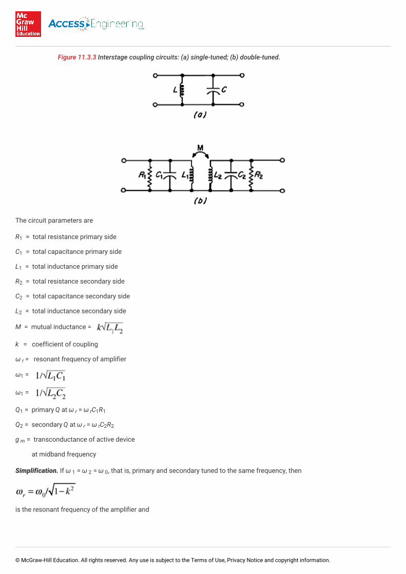
Figure 11.3.3 Interstage coupling circuits: (a) single-tuned; (b) double-tuned.
The circuit parameters are
R = total resistance primary side
C = total capacitance primary side
L = total inductance primary side
R = total resistance secondary side
C = total capacitance secondary side
L = total inductance secondary side
M = mutual inductance =
k = coefficient of coupling
ω = resonant frequency of amplifier
ω =
ω =
Q = primary Q at ω = ω C R
Q = secondary Q at ω = ω C R
g = transconductance of active device
at midband frequency
Simplification. If ω = ω = ω , that is, primary and secondary tuned to the same frequency, then
is the resonant frequency of the amplifier and
1
1
1
2
2
2
r
1
1
1 r r 1 1
2 r r 2 2
m
1 2 0
© McGraw-Hill Education. All rights reserved. Any use is subject to the Terms of Use, Privacy Notice and copyright information.

is the gain at this resonant frequency.
For maximum gain,
and for maximum flatness,
Figure 11.3.4 Selective curves for two identical circuits in a double-tuned interstage circuit, atvarious values of k/k c.
If k is increased beyond k , a double-humped response is obtained.
Overall bandwidth of an n-stage amplifier having equal Q circuits with transitional coupled interstages whose bandwidth is B is
The governing equations for the double-tuned-interstage case are shown above. The response for various degrees of couplingrelated to k = k in the equal-coil-Q case is shown in Fig. 11.3.4.
11.3.1.10. Maximally Flat Staggered Interstage Coupling
T
T C
© McGraw-Hill Education. All rights reserved. Any use is subject to the Terms of Use, Privacy Notice and copyright information.

11.3.1.10. Maximally Flat Staggered Interstage Coupling
This type of coupling consists of n single-tuned interstages that are cascaded and adjusted so that the overall gain function ismaximally flat. The overall cascade bandwidth is B , the center frequency of the cascade is ω , and each stage is a single-tuned circuit whose bandwidth B and center frequency are determined from Table 11.3.1. The gain of each stage at cascadecenter frequency is , where C = sum of output capacitance and input capacitance
to next stage and wiring capacitance of cascade, B = stage bandwidth, ω = center frequency of stage, and ω = centerfrequency of cascade.
Table 11.3.1 Design Data for Maximally Flat Staggered n-tuples
n Name of circuit No. of stages Center frequency of stage Stage bandwidth
2 Staggered pair 2 ω ± 0.35B 0.71B
3 Staggered triple 2 ω ± 0.43B 0.50B
1 ω 1.00B
4 Staggered quadruple 2 ω ± 0.46B 0.38B
2 ω ± 0.19B 0.92B
5 Staggered quintuple 2 ω ± 0.29B 0.81B
2 ω ± 0.48B 0.26B
1 ω 1.00B
6 Staggered sextuple 2 ω ± 0.48B 0.26B
2 ω ± 0.35B 0.71B
2 ω ± 0.13B 0.97B
7 Staggered septuple 2 ω ± 0.49B 0.22B
2 ω ± 0.39B 0.62B
2 ω ± 0.22B 0.90B
1 ω 1.00B
11.3.2. RADIO-FREQUENCY OSCILLATORS
G. Burton Harrold
11.3.2.1. General Considerations
n c
T
0 c
c n n
c n n
c n
c n n
c n n
c n n
c n n
c n
c n n
c n n
c n n
c n n
c n n
c n n
c n
© McGraw-Hill Education. All rights reserved. Any use is subject to the Terms of Use, Privacy Notice and copyright information.

11.3.2.1. General Considerations
Oscillators at rf frequencies are usually of the class A sine-wave-output type.
RF oscillators (in common with audio oscillators) may be considered either as one-port networks that exhibit a negative realcomponent at the input or as two-port-type networks consisting of an amplifier and a frequency-sensitive passive network thatcouples back to the input port of the amplifier. It can be shown that the latter type of feedback oscillator also has a negativeresistance at one port. This negative resistance is of a dynamic nature and is best defined as the ratio between the fundamentalcomponents of voltage and current.
The sensitivity of the oscillator’s frequency is directly dependent on the effective Q of the frequency-determining element andthe sensitivity of the amplifier to variations in temperature, voltage variation, and aging. For example, the effective Q of thefrequency-determining element is important because the percentage change in frequency required to produce thecompensating phase shift in a feedback oscillator is inversely proportional to the circuit Q, thus the larger the effective Q thegreater the frequency stability. The load on an oscillator is also critical to the frequency stability since it affects the effective Qand in many cases the oscillator is followed by a buffer stage for isolation.
It is also desirable to provide some means of stabilizing the oscillator’s operating point, either by a regulated supply, dcfeedback for bias stabilization, or oscillator self-biasing schemes such as grid-leak bias. This stabilizes not only the frequencybut also the output amplitude, by tending to compensate any drift in the active device’s parameters. It is also necessary toeliminate the harmonics in the output since they give rise to cross-modulation products producing currents at the fundamentalfrequency that are not necessarily in phase with the dominant oscillating mode. The use of high-Q circuits and the control of thenonlinearity helps in controlling harmonic output.
11.3.2.2. Negative-Resistance Oscillators
The analysis of the negative-impedance oscillator is shown in Fig. 11.3.5. The frequency of oscillation at buildup is notcompletely determined by the LC circuit but has a component that is dependent upon the circuit resistance. At steady state, thefrequency of oscillation is a function of 1 + R/R or 1 + R /R, depending on the particular circuit where the ratios R/R , R /Rare usually chosen to be small. While R is a fixed function of the loading, R or R /R must change with amplitude duringoscillator buildup, so that the condition of α = 0 can be reached. Thus R , R cannot be constant but are dynamic impedancesdefined as the ratio of the fundamental voltage across the elements to the fundamental current into the element.
iv ic ic iv
ic iv
iv ic
© McGraw-Hill Education. All rights reserved. Any use is subject to the Terms of Use, Privacy Notice and copyright information.

Figure 11.3.5 General analysis of negative-resistance oscillators.
The type of dc load for biasing and the resonant circuit required for the proper operation of a negative-resistance oscillatordepend on the type of active element. R must be less than |R | or R must be greater than |R | in order for oscillation to build upand be sustained.
The detailed analysis of the steady-state oscillator amplitude and frequency can be undertaken by graphical techniques. Themagnitude of G or R is expressed in terms of its voltage dependence. Care must be taken with this representation, since theshape of the G or R curve depends on the initial bias point.
The analysis of negative-resistance oscillators can now be performed by means of admittance diagrams. The assumption foroscillation to be sustaining is that the negative-resistance element, having admittance y , must equal −y , the external circuitadmittance. This can be summarized by G = −G and B = −B . A typical set of admittance curves is shown in Fig. 11.3.6. Inthis construction, it is assumed that B = −B , even during the oscillator buildup. Also shown is the fact that G at zeroamplitude must be larger than G so that the oscillator can be started, that is, α > 0, and that it may be possible to have two ormore stable modes of oscillation.
11.3.2.3. Feedback Oscillators
Several techniques exist for the analysis of feedback oscillators. In the generalized treatment, the active element is representedby its y parameters whose element values are at the frequency of interest, having magnitudes defined by the ratio of thefundamental current divided by fundamental voltage. The general block diagram and equations are shown in Fig. 11.3.7.Solution of the equations given yields information on the oscillator’s performance. In particular, equating the real and imaginaryparts of the characteristic equation gives information on amplitude and frequency of oscillation.
iv ic
i i
i i
i c
i c i c
i c i
c
© McGraw-Hill Education. All rights reserved. Any use is subject to the Terms of Use, Privacy Notice and copyright information.

Figure 11.3.6 Admittance diagram of voltage-stable negative-resistance oscillators: (a) self-startingcase, α > 0; (b) circuit starts oscillating only if externally excited beyond point 1.
In many instances, many simplifications to these equations can be made. For example, if y and y are made small (as invacuum-tube amplifiers), then
This equation can be solved by equating the real and imaginary terms to zero to find the frequency and the criterion foroscillation of constant amplitude. This equation can also be used to draw an admittance diagram for oscillator analysis.
Figure 11.3.7 General analysis of feedback oscillators.
11 12
© McGraw-Hill Education. All rights reserved. Any use is subject to the Terms of Use, Privacy Notice and copyright information.

Figure 11.3.8 Admittance diagram of feedback oscillator.
Figure 11.3.9 S-parameter and analysis of oscillators.
These admittance diagrams are similar to those discussed under negative-resistance oscillators. The technique is illustrated inFig. 11.3.8.
At higher frequencies, the S parameters can also be used to design oscillators (Fig. 11.3.9). The basis for the oscillator is thatthe magnitude of the input reflection coefficient must be greater than unity, causing the circuit to be potentially unstable (inother words, it has a negative real part for the input impedance). The input reflection coefficient with a Γ output termination is
Either by additional feedback or adjustment of Γ it is possible to make . Next, establishing a load Γ such that it
reflects all the energy incident on it will cause the circuit to oscillate. This criterion is stated as
at the frequency of oscillation.
L
L s
© McGraw-Hill Education. All rights reserved. Any use is subject to the Terms of Use, Privacy Notice and copyright information.

This technique can be applied graphically, using a Smith chart as before. Here the reciprocal of is plotted as a function of
frequency since . Now choose either a parallel or a series-tuned circuit and plot its Γ . If f is the frequency common to
and Γ , and satisfies the above criterion, the circuit will oscillate at this point.
11.3.3. BROADBAND AMPLIFIERS
John W. Lunden, Jennifer E. Doyle
11.3.3.1. Introduction
In broadband amplifiers signals are amplified so as to preserve over a wide band of frequencies such characteristics as signalamplitude, gain response, phase shift, delay, distortion, and efficiency. The width of the band depends on the active deviceused, the frequency range, and power level in the current state of the art. As a general rule, above 100 MHz, a 20 percent orgreater bandwidth is considered broadband, whereas an octave or more is typical below 100 MHz. As the state-of-the-artadvances, it is becoming more common to achieve octave-bandwidth or wider amplifiers well into the microwave region usingbipolar and FET active devices.
Hybrid-integrated-circuit techniques and new monolithic techniques eliminate many undesired package and bonding parasiticswhich can limit broadband amplifier performance. Additionally, distributed amplifiers, and other approaches which use multipledevices, have become more economical with increasing levels of integration.
It has become uncommon to use tube devices for new amplifier designs. Solid-state devices have replaced tubes in mostamplifier applications because of superior long-term reliability and lower noise figures. In the following discussion both field-effect and bipolar transistor notations appear for generality.
Figure 11.3.10RC-coupled stages: (a) field-effect transistor form; (b) bipolar junction transistorform.
11.3.3.2. Low-, Mid-, and High-Frequency Performance
Consider the basic common-source and common-emitter-broadband RC coupled configurations shown in Fig. 11.3.10.Simplified low-frequency small-signal equivalent circuits are shown in Fig. 11.3.11.
The voltage gain of the FET amplifier stage under the condition that all reactances are negligibly small is the midband value (atfrequency f)
s 1
s
© McGraw-Hill Education. All rights reserved. Any use is subject to the Terms of Use, Privacy Notice and copyright information.

Figure 11.3.11 Equivalent circuits of the stages shown in F. 11.3.10: (a) FET form; (b) bipolar form.
If the low-frequency effects are included, this becomes
The low-frequency cutoff is because principally of two basic time constants, R C and R C . For C values large enough forthe time constant to be much longer than that associated with C , a low-frequency cutoff or half-power point can bedetermined as
If the coupling capacitor is very large, the low-frequency cutoff is a result of C . The slope of the actual rolloff is a function ofthe relative effect of these two time constants. Therefore, the design of coupling and bypass circuits to achieve very-low-frequency response requires very large values of capacitance.
Similarly, for a bipolar transistor stage, the midband current gain can be determined as
where
g g S S S
g
S
© McGraw-Hill Education. All rights reserved. Any use is subject to the Terms of Use, Privacy Notice and copyright information.
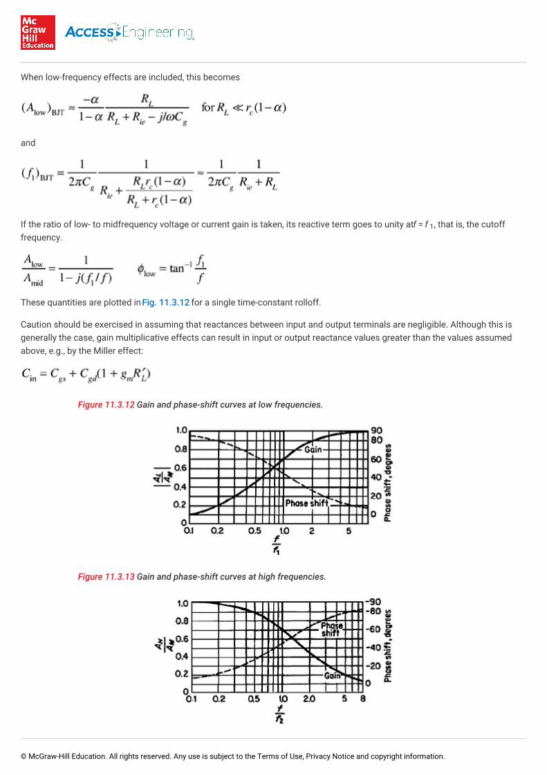
When low-frequency effects are included, this becomes
and
If the ratio of low- to midfrequency voltage or current gain is taken, its reactive term goes to unity at f = f , that is, the cutofffrequency.
These quantities are plotted in Fig. 11.3.12 for a single time-constant rolloff.
Caution should be exercised in assuming that reactances between input and output terminals are negligible. Although this isgenerally the case, gain multiplicative effects can result in input or output reactance values greater than the values assumedabove, e.g., by the Miller effect:
Figure 11.3.12 Gain and phase-shift curves at low frequencies.
Figure 11.3.13 Gain and phase-shift curves at high frequencies.
1
© McGraw-Hill Education. All rights reserved. Any use is subject to the Terms of Use, Privacy Notice and copyright information.
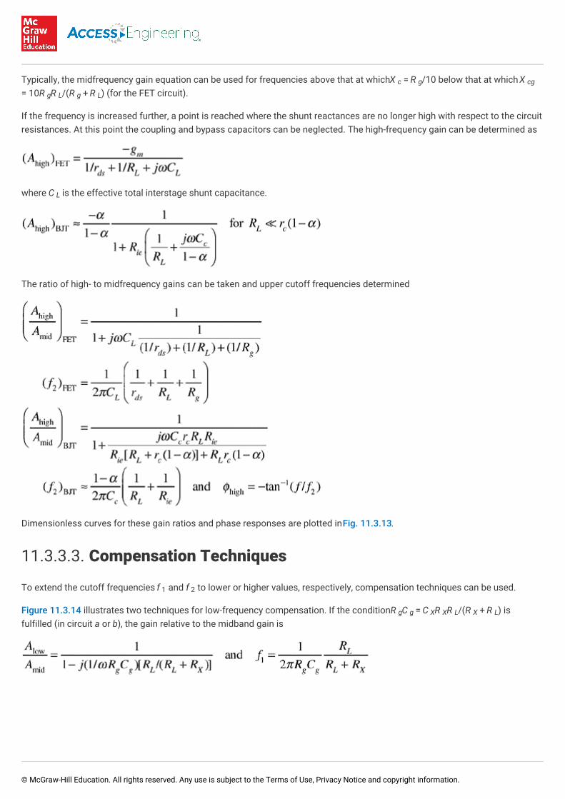
Typically, the midfrequency gain equation can be used for frequencies above that at which X = R /10 below that at which X = 10R R /(R + R ) (for the FET circuit).
If the frequency is increased further, a point is reached where the shunt reactances are no longer high with respect to the circuitresistances. At this point the coupling and bypass capacitors can be neglected. The high-frequency gain can be determined as
where C is the effective total interstage shunt capacitance.
The ratio of high- to midfrequency gains can be taken and upper cutoff frequencies determined
Dimensionless curves for these gain ratios and phase responses are plotted in Fig. 11.3.13.
11.3.3.3. Compensation Techniques
To extend the cutoff frequencies f and f to lower or higher values, respectively, compensation techniques can be used.
Figure 11.3.14 illustrates two techniques for low-frequency compensation. If the condition R C = C R R /(R + R ) isfulfilled (in circuit a or b), the gain relative to the midband gain is
c g cg
g L g L
L
1 2
g g X X L X L
© McGraw-Hill Education. All rights reserved. Any use is subject to the Terms of Use, Privacy Notice and copyright information.

Figure 11.3.14 Low-frequency compensation networks: (a) bipolar transistor version; (b), (c) FETversions.
Hence, improved low-frequency response is obtained with increased values of R . This value is related to R and restricted byactive-device operating considerations. Also, R is dependent on the desired high-frequency response. It can be shown thatequality of time constants R C = R C will produce zero phase shift in the coupling circuit (for R > 1/ωC ). The circuitshown in Fig. 11.3.14c is more critical. It is used with element ratios set to R /R = R /R and C /C = R /R .
Various compensation circuits are also available for high-frequency-response extension. Two of the most common, the series-and shunt-compensation cases, are shown in Fig. 11.3.15. The high-frequency-gain expressions of these configurations can bewritten
The coefficients of the terms decrease rapidly for the higher-order terms, so that if a = b , a = b , etc., to as high an order ofthe f/f ratio as possible, a maximally flat response curve is obtained.
For the phase response, d /dω can also be expressed as a ratio of two polynomials in f/f , and a similar procedure can befollowed. A flat time-delay curve results. Unfortunately, the sets of conditions for flat gain and linear phase are different, andcompromise values must be used.
Shunt Compensation. The high-frequency gain and time delay for the shunt-compensated stage are
X L
L
L X g g X x
L X g c X g c X
1 1 2 2
2
2
© McGraw-Hill Education. All rights reserved. Any use is subject to the Terms of Use, Privacy Notice and copyright information.

where .
A case when R cannot be assumed to be high, such as the input of a following bipolar transistor stage, is considerably morecomplex, depending on the transistor equivalent circuit used. This is particularly true when operating near the transistor f and/or above the VHF band.
Series Compensation. In the series-compensated circuit, the ratio of C to C is an additional parameter. If this can beoptimized, the circuit performance is better than in the shunt-compensated case. Typically, however, control of this parameter isnot available due to physical and active-device constraints.
Figure 11.3.15 High-frequency compensation schemes: (a) shunt; (b) series; (c) shunt-series.
These two basic techniques can be combined to improve the response at the expense of complexity. The shunt-series-compensation case and the so-called “modified” case are examples. The latter involves a capacitance added in shunt with theinductance L or placing L between C and R .
For the modified-shunt case, the added capacitance C permits an additional degree of freedom, and associated parameter, k = C /C .
g
T
s g
s L
c 1
c s
© McGraw-Hill Education. All rights reserved. Any use is subject to the Terms of Use, Privacy Notice and copyright information.

Other circuit variations exist for specific broadband compensation requirements. Phase compensation, for example, may benecessary as a result of cascading a number of minimum-phase circuits designed for flat frequency response. Circuits such asthe lattice and bridged-T can be used to alter the system response by reducing the overshoot without severely increasing theoverall rise time.
11.3.3.4. Cascaded Broadband Stages
When an amplifier is made up of n cascaded RC stages, not necessarily identical, the overall gain A can be written
where f , f ,…, f are the f or f values for the respective stages, depending on whether the overall low- or high-frequency gainratio is being determined. The phase angle is the sum of the individual phase angles. If the stages are identical, f = f = f forall, and
Stagger Peaking. In stagger tuning a number of individual bandpass amplifier stages are cascaded with frequencies skewedaccording to some predetermined criteria. The most straightforward is with the center frequencies adjusted so that the f ofone stage concludes with the f of the succeeding stage, and so forth. The overall gain bandwidth then becomes
A significant simplifying criterion of this technique is stage isolation. Isolation, in transistor stages particularly, is not generallyhigh, except at low frequencies. Hence the overall design equations and subsequent overall alignment can be significantlycomplicated because of the interactions. Complex device models and computer-aided design greatly facilitate theimplementation of this type of compensation. The simple shuntcompensated stage has found extensive use in stagger-tunedpulse-amplifier applications.
11.3.3.5. Transient Response
Time-domain analysis is particularly useful for broadband applications. Extensive theoretical studies have been made of theseparate effects of nonlinearities of amplitude and phase response. These effects can be investigated starting with anormalized low-pass response function.
where a and m are constants describing amplitude-frequency response and b and n are constants describing phase-frequencyresponse. Figure 11.3.16 illustrates the time response to an impulse and a unit-step forcing function for various values of m,with n = 0. Rapid change of amplitude with frequency (large m) results in overshoot. Nonzero, but linear, phase-frequencycharacteristics (n = 1) result in a delay of these responses, without introducing distortion. Further increase in n results inincreased ringing and asymmetry of the time function.
n
a b n 1 2
a b x
2
1
© McGraw-Hill Education. All rights reserved. Any use is subject to the Terms of Use, Privacy Notice and copyright information.

Figure 11.3.16 Transient responses to unit impulse (left) and unit step (right) for various values ofm.
An empirical relationship between rise time (10 to 90 percent) and bandwidth (3 dB) can be expressed as
where K varies from about 0.35 for circuits with little or no overshoot to 0.45 for circuits with about 5 percent overshoot. K is0.51 for the ideal rectangular low-pass response with 9 percent overshoot; for the Gaussian amplitude response with noovershoot, K = 0.41.
The effect on rise time of cascading a number of networks n depends on the individual network pole-zero configurations. Somegeneral rules follow.
Figure 11.3.17 Response to a unit step of n capacitively coupled stages of the same time constant.
1. For individual circuits having little or no overshoot, the overall rise time is
2. If t = t = t ,
3. For individual stage overshoots of 5 to 10 percent, total overshoot increases as .
r1 r2 rn
© McGraw-Hill Education. All rights reserved. Any use is subject to the Terms of Use, Privacy Notice and copyright information.

4. For circuits with low overshoot (~1 percent), the total overshoot is essentially that of one stage.
The effect of insufficient low-frequency response of an amplifier is sag of the time response. A small amount of sag (<10percent) can be described by the formula
where T is one-half period of a square-wave voltage.
Figure 11.3.17 illustrates the response to a step function of n capacitor-coupled stages with the same time constant. The effectof arithmetic addition of individual stage initial slopes determining the net total initial transition slope can be seen.
11.3.3.6. Distributed Amplifiers
This technique is useful for operation of devices at or near the high-frequency limitation of gain bandwidth. While the individualstage gain is low, the stages are cascaded so that the gain response is additive instead of multiplicative. The basic principle isto allow the input and output capacitances to form the shunt elements of two delay lines. This is shown in Fig. 11.3.18.
If the delay times per section in the two lines are the same, the output signals traveling forward add together without relativedelay. Care must be taken to ensure proper terminating conditions. The gain produced by n devices, each of transconductanceg , has a value of G = ng Z /2. Performance to very low frequencies can be achieved. The high-frequency limit is determinedby the cutoff frequencies of the input and output lines or effects within the active devices themselves other than parasitic shuntcapacities (e.g., transit time or alpha-fall-off effects).
For input and output lines of different characteristic impedances, the overall gain is given by
Figure 11.3.18 Distributed amplifier circuits: (a) FET version; (b) bipolar transistor version.
m m 02
© McGraw-Hill Education. All rights reserved. Any use is subject to the Terms of Use, Privacy Notice and copyright information.

The characteristic impedances and cutoff frequencies are given as
There does not seem to be an optimum choice for Z ; a device with a high figure of merit is simply chosen, and the restfollows. There is, however, an optimum way in which N devices can be grouped, namely, in m identical cascaded stages, eachwith n devices, so that N is a minimum for a given overall gain A. N is a minimum when m = ln A. Consequently, the optimumgain per stage G = e = 2.72.
Various techniques are utilized to determine the characteristics of the lumped transmission lines. Constant-K and m-derivedfilter sections are most common, augmented by several compensation circuit variations. The latter include paired gate-drain(base-collector), bridged-T, and resistive loading connections. The constant-K lumped line has several limitations, including thefact that the termination is not a constant resistance and that impedance increases with frequency and time delay alsochanges with frequency.
m-derived terminating half sections and time-delay equalizing sections result in a frequency-amplitude response that is quiteflat at very high frequencies.
The effects of input loading and/or line loss modify the gain expression to
where = the real part of propagation constant γ and
The design of distributed amplifiers using bipolar transistors is more difficult because of the low input impedance. In addition,the intrinsic gain of the transistor (β or α) is a decreasing function of frequency.
The simplest approach in overcoming this problem is to connect a parallel RC in series with the base, as shown in Fig. 11.3.18b.By setting RC = β /2πf , the gain is made essentially independent of frequency up to about f /2, with an overall voltage gain of
where m is the number of stages and n is the number of transistors per stage.
The increasing impedance of the constant-K line helps keep the frequency response flat, compensating for the increasedloading of the bipolar transistor.
Another bipolar transistor approach involves the division of the frequency range into three regions to account for the losses.Each region is associated with a linear-Q variation with frequency of the transistor input-output circuits, approximated by shuntRC elements.
The lossless voltage gain is
02
0 T T
© McGraw-Hill Education. All rights reserved. Any use is subject to the Terms of Use, Privacy Notice and copyright information.

In region I, the input impedance is high and the transistor supplies high voltage gain. In regions II and III, the voltage gains aregiven by
where K = (f /f )
K = 1
f = frequency of min Q
11.3.3.7. Broadband Matching Circuits
Broadband impedance transformation interstage-coupling matching can be achieved with balun transformers, quarter-wavetransmission-line sections, lumped reactances in configurations other than discussed above, and short lengths of transmissionlines.
Balun Transformers. In conventional coupling transformers, the interwinding capacitance resonates with the leakageinductance, producing a loss peak. This limits the high-frequency response. A solution is to use transmission-line transformersin which the turns are arranged physically to include the interwinding capacitance as a component of the characteristicimpedance of a transmission line. With this technique, bandwidths of hundreds of megahertz can be achieved. Good couplingcan be realized without resonances, leading to the use of these transformers in power dividers, couplers, hybrids, and so forth.
Typically, the lines take the form of twisted wire pairs, although coaxial lines can also be used. In some configurations, thelength of the line determines the upper cutoff frequency. The low-frequency limit is determined by the primary inductance. Thelarger the core permeability the fewer the turns required for a given low-frequency response. Ferrite toroids have been found tobe satisfactory with widely varying core-material characteristics. The decreasing permeability with increasing frequency isoffset by the increasing reactance of the wire itself, causing a wide-band, flat-frequency response.
Quarter-Wave Transformers. The quarter-wavelength line transformer is another well-known element. It is simply atransmission line one-quarter wavelength long, with a characteristic impedance
where Z and Z are the terminating impedances. The insertion loss of this line section is
where r = Z /Z and θ = 2πL/λ = 90° at f .
Figure 11.3.19 shows the bandwidth performance of the quarter-wave line for several matching ratios. Such lines may becascaded to achieve broader-band matching by reducing the matching ratio required of each individual section.
II c Q2
III
Q
in out
in out 0
© McGraw-Hill Education. All rights reserved. Any use is subject to the Terms of Use, Privacy Notice and copyright information.

Figure 11.3.19 Bandwidth of a quarter-wave matching transformer.
Lumped and Pseudo-Lumped Transformations. The familiar lumped-element ladder network, depending on the element valuesand realization, approximates a short-step transmission-line transformer or a tapered transmission line.
11.3.3.8. Feedback and Gain Compensation
Feedback. The bandwidth of amplifiers can be increased by the application of inverse feedback. A multiplicity of feedbackcombinations and analysis techniques are available and extensively treated in the literature. In addition, the related concept offeedforward has been investigated and successfully implemented. Figure 11.3.20 shows four feedback arrangements andformulas describing their performance. A major consideration, particularly for rf applications, is the control of impedance andloop-delay characteristics to ensure stability.
Gain Compensation. The power gain of a bipolar transistor amplifier typically falls 6 dB/octave with increasing frequency abovethe f value. The gain can be leveled (bandwidth-widened) by exact matching of the source impedance to the device at theupper frequency only, causing increasing mismatch with decreasing frequency and the associated gain loss. The overall flatgain is the value at the high best-match frequency. Sufficient resistive loss is usually required in this interstage to preventinstabilities in either driver or driven stage because of the mismatch unloading.
11.3.3.9. Power-Combining Amplifiers
Many circuit techniques have been developed to obtain relatively high output powers with given modestpower devices. Twoapproaches are the direct-paralleling and hybrid splitting-combining techniques. The direct-paralleling approach is limited bydevice-to-device variations and the difficulties in providing balanced conditions because of the physical wavelengthrestrictions. A technique commonly used at UHF and microwave frequencies to obtain multioctave response incorporatesmatched stages driven from hybrid couplers in a balanced configuration. The coupler offers a constant-source impedance(equal to the driving-port impedance) to the two stages connected to its output ports. Power reflected because of the identicalmismatches is coupled to the difference port of the hybrid and dissipated in the idler load. The hybrid splitting-combiningapproach has proved quite effective in implementing high-output-level requirements (e.g., kilowatts at 1.4 GHz with bipolartransistors).
β
© McGraw-Hill Education. All rights reserved. Any use is subject to the Terms of Use, Privacy Notice and copyright information.

Figure 11.3.20 Four methods of applying feedback, showing influence on gain and input and outputimmittances (From Hakim “Junction Transistor Circuit Analysis,” by permission of John Wiley &Sons, New York).
The hybrid splitting-combining approach enhances circuit operation. In particular, quadrature hybrids affect a voltage standingwave ratio (VSWR)-canceling phenomenon that results in extremely well-matched power-amplifier inputs and outputs that canbe broadbanded on proper selection of particular hybrid trees. Also, the excellent isolation between devices makes reliablepower-amplifier service possible.
© McGraw-Hill Education. All rights reserved. Any use is subject to the Terms of Use, Privacy Notice and copyright information.
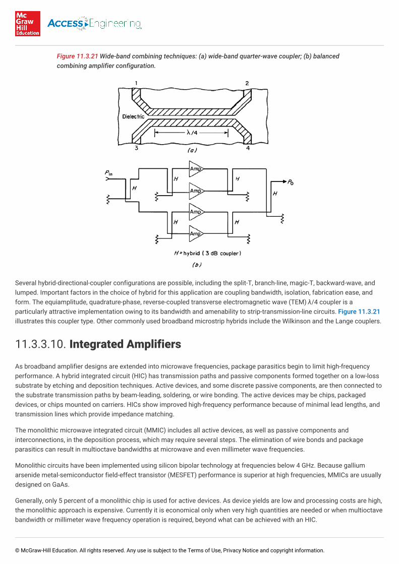
Figure 11.3.21 Wide-band combining techniques: (a) wide-band quarter-wave coupler; (b) balancedcombining amplifier configuration.
Several hybrid-directional-coupler configurations are possible, including the split-T, branch-line, magic-T, backward-wave, andlumped. Important factors in the choice of hybrid for this application are coupling bandwidth, isolation, fabrication ease, andform. The equiamplitude, quadrature-phase, reverse-coupled transverse electromagnetic wave (TEM) λ/4 coupler is aparticularly attractive implementation owing to its bandwidth and amenability to strip-transmission-line circuits. Figure 11.3.21illustrates this coupler type. Other commonly used broadband microstrip hybrids include the Wilkinson and the Lange couplers.
11.3.3.10. Integrated Amplifiers
As broadband amplifier designs are extended into microwave frequencies, package parasitics begin to limit high-frequencyperformance. A hybrid integrated circuit (HIC) has transmission paths and passive components formed together on a low-losssubstrate by etching and deposition techniques. Active devices, and some discrete passive components, are then connected tothe substrate transmission paths by beam-leading, soldering, or wire bonding. The active devices may be chips, packageddevices, or chips mounted on carriers. HICs show improved high-frequency performance because of minimal lead lengths, andtransmission lines which provide impedance matching.
The monolithic microwave integrated circuit (MMIC) includes all active devices, as well as passive components andinterconnections, in the deposition process, which may require several steps. The elimination of wire bonds and packageparasitics can result in multioctave bandwidths at microwave and even millimeter wave frequencies.
Monolithic circuits have been implemented using silicon bipolar technology at frequencies below 4 GHz. Because galliumarsenide metal-semiconductor field-effect transistor (MESFET) performance is superior at high frequencies, MMICs are usuallydesigned on GaAs.
Generally, only 5 percent of a monolithic chip is used for active devices. As device yields are low and processing costs are high,the monolithic approach is expensive. Currently it is economical only when very high quantities are needed or when multioctavebandwidth or millimeter wave frequency operation is required, beyond what can be achieved with an HIC.
11.3.4. TUNNEL-DIODE AMPLIFIERS
© McGraw-Hill Education. All rights reserved. Any use is subject to the Terms of Use, Privacy Notice and copyright information.

11.3.4. TUNNEL-DIODE AMPLIFIERS
Chang S. Kim
11.3.4.1. Introduction
Tunnel-diode (TD) amplifiers are one-port negative-conductive devices. Hence the problems associated with them are quitedifferent from those encountered in conventional amplifier design. Circuit stabilization and isolation between input and outputterminals are primary concerns in using this very wide-frequency-range device.
Although there are several possible amplifier configurations, the following discussion is limited to the most practical design,which uses a circulator for signal isolation. The advantage of the circulator-coupled form of tunnel-diode amplifier resides inthe fact that it is thereby possible to convert a bilateral one-port amplifier into an ideal unilateral two-port amplifier. Tunneldiodes can provide amplification at microwave frequencies with a relatively simple structure and at a low noise figure.
11.3.4.2. Tunnel Diodes
Three kinds of tunnel diodes are available, namely, those using Ge, GaAs, and GaSb. V-I characteristics and correspondingsmall-signal conductance-voltage relationships are shown in Figs.11.3.22 and 11.3.23, respectively. A typical small-signaltunnel-diode equivalent circuit is shown in Fig. 11.3.24. Here g , C , r , L, and C are the small-signal conductance, junctioncapacitance, series resistance, series inductance, and shunt capacitance, respectively. Noise generators e and i are includedfor subsequent discussion.
Figure 11.3.22 Characteristics of tunnel diodes.
j j s p
s j
© McGraw-Hill Education. All rights reserved. Any use is subject to the Terms of Use, Privacy Notice and copyright information.

Figure 11.3.23 Voltage-vs.-g j characteristics of tunnel diodes of F. 11.3.22.
Figure 11.3.24 Small-signal equivalent circuit of tunnel-diode amplifier.
11.3.4.3. Stability
The stability criteria are derived from the immittance expression across the diode terminals and are quite complicated.
Using the short-circuit stable condition, the stability criteria can be simplified considerably. With reference to Fig. 11.3.24, withthe external circuit connected, the total admittance Y across g can be expressed as
where Y (s), the admittance facing g , is a positive real function. Since Y is connected in parallel with a short-circuit stabledevice with negative conductance g , Y is short-circuit-stable. This implies that, since q(s) is always a Hurwitz polynomial, thestability condition is that p(s) must also be Hurwitz polynomial.
A simple graphical interpretation of this stability condition is as follows. The plot of Y (ω) can be obtained from the plot of Y(ω) by shifting the imaginary axis by |g | along the real axis, as shown in Fig. 11.3.25. Since q(s) has no roots in the right halfplane, any encirclement of the origin of Y (ω) must come from the right-half-plane roots of p(s) only. Therefore, the circuit willbe stable if and only if Y (ω) does not encircle the origin (Fig. 11.3.25a). If g becomes large so that the origin is encircled by Y(ω) (Fig. 11.3.25b), the circuit is unstable.
11.3.4.4. Tunnel-Diode-Amplifier Design
T j
i j i
i T
[*]T
i j
T
T j
T
© McGraw-Hill Education. All rights reserved. Any use is subject to the Terms of Use, Privacy Notice and copyright information.

A simplified block diagram of a circulator-coupled TD amplifier is shown in Fig. 11.3.26. The three basic circuit parts are thetunnel diode, the stabilizing circuit, and the tuning circuit, which includes a four-port circulator. The following conditions areimposed on the amplifier design:
1. In the band
a. G = Re Y is slightly larger than |g |.
b. G is contributed by the tuning circuit only.
c. B = Im Y = 0 at the center frequency f and small in the band.
2. Outside the band
a. G = Re Y is larger than |g |
b. If G ≤ |g |, B should not be zero.
To satisfy these conditions, a stabilizing circuit, shown in Fig. 11.3.26, is required. This circuit is designed so that the followingrelationships are satisfied:
where f is the center frequency.
Figure 11.3.25 Representative plots of real and imaginary parts of Y T: (a) stable condition; (b)unstable condition.
The equivalent circuit of Fig. 11.3.24 can be transformed into the parallel equivalent circuit of Fig. 11.3.27. The followingidentities relate the parameters of Figs. 11.3.24 and 11.3.27:
i i j
i
i i 0
i i j
i j j
0
© McGraw-Hill Education. All rights reserved. Any use is subject to the Terms of Use, Privacy Notice and copyright information.

Figure 11.3.26 Tunnel-diode amplifier using circulator.
Figure 11.3.27 Parallel version of equivalent circuit of F. 11.3.24.
The gain can be expressed by
where B − B = 0 at f = f , in which B is the reactive part of Y .
In this case, the tuning circuit is a more general matching circuit using combinations of parallel and series transmission lines. Itshould be noted that |Γ| becomes 1, or g = |g |, as the operating frequency increases to f , the resistive cutoff frequency,which is defined by
It is desirable to have a device with f several times (at least three) larger than f . Furthermore, it is desirable to make the self-resonance frequency f ,
e 0 e e
sp jp r
r 0
x
© McGraw-Hill Education. All rights reserved. Any use is subject to the Terms of Use, Privacy Notice and copyright information.

as high as possible (higher than f ) to improve the stability margin.
The gain expression can be modified to include the input amplifier admittance Y of Fig. 11.3.26 as follows:
Similarly, the bandwidth can be determined from the expression for Γ and f , above.
Typical germanium tunnel-diode parameters pertinent to S-, C-, and X-band amplifiers with approximate gains to 10 dB areshown in Table 11.3.2.
11.3.4.5. Noise Figure in TD Amplifiers
A noise equivalent circuit can be completed by inserting a current generator, and a voltage generator , as shown in Fig.
11.3.24 (dotted lines). The mean-square values are determined from
where I = equivalent shot-noise current = I = dc current in negative-conductance region.
Table 11.3.2 Typical Germanium Tunnel-Diode Parameters
S band C band X band
|r | = 1/g , Ω 70 70 70
C , pF <1 <0.5 <0.2
L, H <0.1 <0.1 <0.2
r , Ω <0.1r <0.1r <0.1r
The noise equivalent circuit of Fig. 11.3.24 can be transformed into a parallel-equivalent circuit of Fig. 11.3.27 having current
generators and (dotted lines); and can be derived from the two equivalent circuits to be
where G = eI /2KT = 20I at room temperature.
Tunnel diodes provide good noise performance with a relatively simple amplifier structure requiring only a dc source for bias. Itis therefore a useful low-noise, small-signal amplifier for microwave applications.
c
a
2x
eq dc
j j
j
s j j j
eq eq eq
© McGraw-Hill Education. All rights reserved. Any use is subject to the Terms of Use, Privacy Notice and copyright information.

11.3.5. PARAMETRIC AMPLIFIERS
Conrad E. Nelson
11.3.5.1. Introduction
The term parametric amplifier (paramp) refers to an amplifier (with or without frequency conversion) using a nonlinear or time-varying reactance. Development of low-loss variable-capacitance (varactor) diodes resulted in the development of varactor-diode parametric amplifiers with low noise figure in the microwave frequency region. Types of paramps include one-port, two-port (traveling-wave), degenerate (pump frequency twice the signal frequency), nondegenerate, multiple pumps, and multipleidlers. The most widely used amplifier is the non-degenerate one-port paramp with a circulator, because it achieves very goodnoise figures without undue circuit complexity.
11.3.5.2. One-Port Paramp with Circulator
© McGraw-Hill Education. All rights reserved. Any use is subject to the Terms of Use, Privacy Notice and copyright information.

11.3.5.2. One-Port Paramp with Circulator
The one-port paramp with circulator is illustrated in Fig. 11.3.28, and the simplified circuit diagram is shown in Fig. 11.3.29. Theinput signal and the amplified output signal (at the same frequency) are separated by the circulator. The cw pump source iscoupled to a back-biased varactor to drive the nonlinear junction capacitance at the pump frequency. The signal and pumpcurrents mix in the nonlinear varactor to produce voltages at many frequencies. The additional (idler) filter allows only thedifference or idler current to flow at the idler frequency; i.e.,
Figure 11.3.28 One-port parametric amplifier and circulator.
The idler current remixes with the pump current to produce the signal frequency again. The phasing of this signal due tononlinear reactance mixing is such that the original incident signal is reenforced (i.e., amplified) and reflected back to thecirculator. The one-port paramp at band center is essentially a negative-resistance device at the signal frequency.
Figure 11.3.29 Circuit of one-port paramp using single-tuned resonators.
11.3.5.3. Power Gain and Impedance Effects
© McGraw-Hill Education. All rights reserved. Any use is subject to the Terms of Use, Privacy Notice and copyright information.
11.3.5.3. Power Gain and Impedance Effects
The one-port paramp power gain at the signal frequency is
where R is the signal-circuit equivalent generator resistance and Z is the input impedance at the signal frequency.
For a single-tuned signal circuit and a single-tuned idler circuit the input impedance at the signal frequency is
The diode loss resistance R has been modified at the signal and idler frequencies to include circuit losses (that is, β ≥ 1). Thesignal and idler reactances are X and X , respectively, and must include the varactor junction capacitance. (In the simplifiedcircuit the diode package capacitance has been neglected.) For a fully pumped varactor the cutoff frequency is
where C is the junction capacitance at reverse breakdown. The modulation ratio m for an abrupt-junction diode is 0.25.
11.3.5.4. Bandwidth and Noise
Factors that determine the overall paramp bandwidth include the varactor characteristics (cutoff frequency, junction andpackage capacitance, and lead inductance), choice of idler (pump) frequency, the nature of the signal and idler resonant circuitsand the choice of band-center gain. Multiple-tuned signal and idler circuits are often used to increase the overall parampbandwidth.
At band center the effective noise temperature of the one-port paramp (due to the diode and circuit loss resistances at thesignal and idler frequencies) is
where T is the temperature of varactor junction and loss resistances. The effective noise temperature can be reduced bycooling the paramp below room temperature and/or by proper choice of pump frequency. Circulator losses must be includedwhen determining the overall paramp noise figure.
11.3.5.5. Pump Power
The pump power required at the diode to fully drive a single varactor is
where the pump circuit loss resistance and diode resistance = β R , and k = 0.5 for an abrupt-junction varactor.
11.3.5.6. Gain and Phase Stability
g in
d
s i
R 1
d
p d 1
© McGraw-Hill Education. All rights reserved. Any use is subject to the Terms of Use, Privacy Notice and copyright information.

11.3.5.6. Gain and Phase Stability
The stability of the cw pump source (amplitude and frequency) is a significant factor in the overall paramp gain and phasestability. For small pump-power changes an approximate expression for the paramp power-gain variation is
Environmental temperature changes often require a temperature-regulated enclosure for the paramp and pump source.
At low levels of nonlinear distortion, the amplifier third-order relative power intermodulation product at band center is a functionof the one-port amplifier gain and the incident signal power level; i.e.,
Thus low-band-center amplifier gains reduce this nonlinear distortion.
11.3.6. MASER AMPLIFIERS
Gunter K. Wessel
11.3.6.1. Introduction
A maser is a microwave active device whose name is an acronym derived from microwave amplification by stimulatedemission of radiation. A laser is an amplifier or oscillator also based on stimulated emission but operating in the optical part ofthe spectrum. The expressions microwave, millimeter, submillimeter, infrared, optical, and ultraviolet maser are also incommon use. Here the word maser is used for the whole frequency range of devices, the m standing for molecular.
A description of the laser principle, some of its properties and means of achieving laser operations, is given in Sec. 9.
In these devices, no tubes or transistors are employed in the radiation process, but the properties of atoms or molecules—asgases, liquids, or solids—serve for the amplification of the signals. Oscillators require the addition of a feedback mechanism.The interaction of the electromagnetic radiation with the maser material occurs in a suitable cavity or resonance structure. Thisstructure often serves the additional purpose of generating a desired phase relationship between different spatial parts of thesignal. The application of external energy, required for the amplification or oscillation process, is referred to as pumping. Thepumping power consists, in many cases, of external electromagnetic radiation of a different frequency (usually higher) fromthat for the signal.
Microwave masers are used as low-noise preamplifiers and as time and frequency standards. The stimulated emissionproperties of atoms and molecules at optical frequencies, with their relatively high noise content, make the laser more usefulfor high-power light amplification and oscillation.
11.3.6.2. Maser Principles
© McGraw-Hill Education. All rights reserved. Any use is subject to the Terms of Use, Privacy Notice and copyright information.

In the processes of emission and absorption, atoms or molecules interact with electromagnetic radiation. It is assumed thatthe atoms possess either sharp internal-energy states or broader energy bands. A change of internal energy from one state toanother is accompanied by absorption or emission of electromagnetic radiation, depending on the direction of the process. Thedifference in energy from the original to the final state is proportional to the frequency of the radiation, the proportionalityconstant being Planck’s constant h.
The processes of the spontaneous emission and absorption were defined by Einstein.
Spontaneous emission:
(1)
Absorption:
(2)
where N and N are population densities of atoms or molecules of material having energy states E and E and an energyseparation E − E = hv between them, and A and B are the Einstein coefficients.
At high temperature, an inconsistency in the equilibrium system arises unless a second emission process, stimulated emission,takes place. The rate of stimulated emission is defined very similarly to that of absorption (the stimulated emission issometimes called negative absorption):
(3)
In temperature equilibrium, the rates of emission must be equal to the rate of absorption
(4)
Assuming that the ratio of the population densities is equal to the Boltzmann factor,
(5)
Equation (4) yields, for the radiation density,
(6)
Equation (6) is identical with Planck’s radiation law if we set
(7a)
and
1 2 1 2
2 1 12 21 12
[*]
© McGraw-Hill Education. All rights reserved. Any use is subject to the Terms of Use, Privacy Notice and copyright information.
(7b)
where c is the velocity of light.
Equation (7a) shows the close relationship between stimulated emission and absorption. The rates of population decrease, forthese two processes [Eqs. (2) and (3)] depend only on their respective population densities.
Neglecting the spontaneous emission, the net absorption or the net stimulated emission of an incoming radiation depends,therefore, only on the difference in population density: for absorption, if (N − N ) > 0; for amplification, if (N − N ) < 0. Inparticular, if a system is in quasiequilibrium such that the upper energy state E is more populated than the lower one, E , it iscapable of amplifying electromagnetic radiation.
To create and maintain the quasiequilibrium requires application of external energy since the natural equilibrium has theopposite population excess (N > N ). Different masers differ widely in the methods of how to accomplish the reverse inpopulation density.
11.3.6.3. Properties of Masers
The properties of masers can be understood by analyzing Eqs. (1) to (7b), as follows.
Signal-to-Noise Ratio. From Eqs. (1) and (3) it follows that the Einstein coefficients A and B have different dimensions but theratio B μ/A is dimensionless. Here μ is proportional to the strength of the incoming signal and B μ is proportional to theamplified signal strength. A is proportional to the noise contribution because of spontaneous emission. After rewriting Eq.(7b),
(8)
the ratio is found to be proportional to the signal-to-noise ratio of the amplifier. It thus becomes clear that the noise contribution(thermal or Johnson noise) is very small at microwave frequencies, whereas it becomes very large at optical frequencies (anincrease of 15 orders of magnitude for an increase of 5 orders for the frequency). Microwave masers are therefore very usefulas low-noise microwave preamplifiers.
Infrared, optical, and ultraviolet masers (lasers), on the other hand, are commonly used for power amplification and as powerfullight sources (oscillators). The high content of spontaneous-emission noise does not make them easily applicable for low-noiseamplification or sensitive detection of light, except in a few special cases.
11.3.6.4. Linearity and Line Width
1 2 1 2
2 1
1 2
21 21 21
21
© McGraw-Hill Education. All rights reserved. Any use is subject to the Terms of Use, Privacy Notice and copyright information.

11.3.6.4. Linearity and Line Width
The proportionality between the incoming signal strength, the radiation density μ, and the amplified signal strength means thata maser is a linear amplifier as long as it is not driven into saturation. The latter occurs when the excess population becomes N – N ≈ N .
Line Width. In the absence of a strong interaction of the individual atoms of the material, either with the environment or witheach other, the line width is determined by the average length of time of interaction of an atom with the radiation field. However,if regeneration because of feedback is taking place, the line width may be much narrower because of the following effect. It isassumed that the incoming radiation has a frequency distribution, as shown in Fig. 11.3.30. The amplified signal is proportionalto the rate of stimulated emission dN /dt. According to Eq. (3), the latter is proportional to μ(v ). Thus the center portions ofthe line will be more amplified than the wings, leading to increasingly narrower line widths. In an oscillator the final width isultimately limited by statistical fluctuations because of the quantum nature of the radiation.
Figure 11.3.30 Frequency distribution of radiation incoming to maser.
The narrow line width coupled with the low-noise property of a microwave maser makes the latter useful as a time andfrequency standard device. To reduce interaction, gases are used as microwave maser materials.
In low-noise microwave amplifiers one is usually interested in a relatively large bandwidth (typically 50 MHz or more). For suchamplifier solid-state materials are used, with strong spin-spin interactions of atoms (for example, Cr in ruby).
11.3.6.5. Tuning
Solid-state microwave masers can be tuned over a wide range of frequencies by adjustment of an external magnetic field, whilethe relative tuning range by a magnetic field is smaller by a factor of 10 to 10 in optical masers. Generally, in lasers, onehas to depend on fixed frequencies wherever a suitable spectral line occurs in the material; however, modern liquid-dye laserscan be tuned over a relatively wide range in the visible spectrum.
11.3.6.6. Power Output
2 1 2
2 12
3+
–4 –5
© McGraw-Hill Education. All rights reserved. Any use is subject to the Terms of Use, Privacy Notice and copyright information.

11.3.6.6. Power Output
The power output owing to stimulated emission depends on the number of excess atoms (N − N ) available for the transition.Assuming p to be the probability of a transition per second, the power output is given by
(9)
Equation (9) shows that the power output of a microwave gas maser must be very low (for example, 100 to 1 pW) because thepopulation density and the frequency are small. On the other hand, solid-state lasers and some gas lasers with very highefficiencies may have cw power outputs of 1000 W and more.
11.3.6.7. Coherence
The similarity between absorption and stimulated emission [as expressed in Eqs. (2), (3), and (7a)] means that the stimulatedemission is a coherent process. In practice, this means that a beam of radiation will be amplified only in the direction ofpropagation of the incoming beam and when all atoms participate coherently in the amplification. This is very different from thenoise-producing spontaneous emission, where the radiation is emitted isotropically and no phase relationship exists betweenthe radiation coming from different atoms.
The coherence of the stimulated emission enables one to produce coherent light and radiation patterns similar to those whichare well known and applied in the radio and microwave parts of the spectrum. In particular, it is possible by a suitable geometryof the device to produce a plane-parallel light beam whose divergence angle is limited only by diffraction. The divergence angleis given by
(10)
11.3.6.8. Time and Frequency Standards
The ammonia and hydrogen atomic-beam masers are used as time and frequency standards with operating frequencies ofabout 24 GHz and about 1.4 GHz, respectively. The reverse of population difference is achieved by focusing atoms in theexcited state into a suitable microwave cavity, whereas the atoms in the lower state are defocused by a special focuser and donot reach the interior of the cavity. The microwave field in the cavity causes stimulated emission and amplification. If the cavitylosses can be overcome, oscillations will set in. Time and frequency accuracy of 1 part in 10 or higher can be obtained withmodern maser standard devices.
11.3.6.9. Three- and Four-Level Devices
2 1
12
© McGraw-Hill Education. All rights reserved. Any use is subject to the Terms of Use, Privacy Notice and copyright information.

11.3.6.9. Three- and Four-Level Devices
In many of the masers of all frequency regions, population reverse is obtained by a three-level-maser method first described byBloembergen. Radiation from an external power source at the pumping frequency v (Fig. 11.3.31) is applied to the material. E may be a band to make the pumping more economical. The material is contained in a suitable cavity, a slow-wave structure, orother resonance structure which is resonant at the signal frequency v . Under favorable conditions of the pumping power, thefrequency ratio v /v , and the involved relaxation times, an excess population in the excited state E over the ground state E can be obtained. The interaction with the electromagnetic field of frequency v causes stimulated emission. Thus amplification(and if required, oscillation) is produced.
Figure 11.3.31 Three-level maser.
Figure 11.3.32 Four-level maser.
The four-level maser (Fig. 11.3.32) percent has the additional advantage that the population of the ground state does not haveto be reduced to less than 50 percent of its original equilibrium value and the level E can remain a relatively wide band. Thetransfer of energy from E to E , and E to E , is by spontaneous decay or some other means like spin-lattice relaxation. Mostsolid-state microwave and optical masers are of the three-or four-level variety.
11.3.6.10. Semiconductor Lasers
Stimulated light emission can be obtained by carrier injection in certain semiconductor materials. Upon application of anexternal dc potential, recombination light emission can take place at the interface of an n- and p-type semiconductor (forexample, Zn and Te in GaAs). The semiconductor laser requires only a very simple power source (a few volts of direct current).However, the laser material has to be cooled to liquid-nitrogen temperature and the power output is relatively low.
11.3.6.11. Applications
p 3
s
s p 2 1
s
4
4 1 2 1
© McGraw-Hill Education. All rights reserved. Any use is subject to the Terms of Use, Privacy Notice and copyright information.

11.3.6.11. Applications
The particular properties of devices based on stimulated emission have resulted in numerous applications which often surpassthe capabilities of standard devices. In some instances, e.g., holography, new fields have opened up through the emergence oflasers and masers.
Solid-state microwave preamplifiers for communication, radar, and radio astronomy have by far the best signal-to-noise ratio ofall microwave amplifiers. The hydrogen-beam maser is the most accurate of all frequency and time standards.
Lasers have revolutionized the field of optical instrumentation and spectroscopy. They have made possible the new field ofnonlinear optics. The laser is or may be used in many applications where large energy densities are required, as inmicrowelding, medical surgery, or even in cracking rocks in tunnel building. Lasers can be used as communication media whereextremely large bandwidths are required. Optical radar, with its high precision owing to the short wavelength, uses lasers aspowerful, well-collimated light sources. Their range extends as far as the moon.
11.3.7. ACOUSTIC AMPLIFIERS
Stephen W. Tehon, Y. J. Lin, Wen-Chung. Wang
11.3.7.1. Acoustoelectric Interaction
© McGraw-Hill Education. All rights reserved. Any use is subject to the Terms of Use, Privacy Notice and copyright information.

11.3.7.1. Acoustoelectric Interaction
The acoustic amplifier stems from the announcement by Hutson, McFee, and White, in 1961, that they had observed a sizableinfluence on acoustic waves in single crystals of CdS caused by a bias current of change carriers. CdS is both a semiconductorand piezoelectric crystal, and the interaction was found to involve an energy transfer via traveling electric fields generated byacoustic waves, producing, in turn, bunching of the drift carriers. Quantitative analyses showing that either loss or gain in wavepropagation could be selected by controlling the drift field were published by White.
Figure 11.3.33 Traveling wave of electric field intensity induced by traveling stress wave.
Figure 11.3.34 Normalized gain as a function of bias field.
Figure 11.3.33 illustrates the nature of the interaction. As an acoustic wave propagates in the crystal its stresses induce asimilar pattern of electric field through piezoelectric coupling. Since the coupling is linear, compressive stresses in half thewave induce a forward-directed field, and tensile stresses in the remainder of the wave induce a backward-directed field.Drifting charge carriers tend to bunch at points of zero field to which they are forced by surrounding fields. When a chargecarrier loses velocity in bunching, it gives its excess kinetic energy to the acoustic wave; when it gains velocity, it extractsenergy from the wave. Therefore the drift field is effective for determining attenuation or amplification in the range near whichcarriers move at the speed of sound. Figure 11.3.34 illustrates the gain characteristic as a function of drift velocity. At the zero-crossover point, the carrier velocity is just equal to the velocity of propagation for the acoustic wave; the gain ranges frommaximum attenuation up to maximum amplification over a relatively small change in bias. Beyond this range of drift velocity,bunching becomes decreasingly effective, and the interaction has less effect on the acoustic wave.
11.3.7.2. Piezoelectric Materials
© McGraw-Hill Education. All rights reserved. Any use is subject to the Terms of Use, Privacy Notice and copyright information.

11.3.7.2. Piezoelectric Materials
Piezoelectricity is the linear, reversible coupling between mechanical and electric energy because of displacement of chargesbound in molecular structure. Pressure applied to a piezoelectric material produces a change in observed surface density ofcharge, and conversely, charge applied over the surfaces produces internal stress and strain. If S is the strain, T the stress, E theelectric field intensity, and D the dielectric displacement, the piezoelectric effect at a point in a medium is described by the pairof linear equations
where constant s = elastic compliance
= permittivity
d = piezoelectric constant
The ratio , calculated from these constants for a particular piezoelectric material, is defined as K , where K is thecoefficient of electromechanical coupling. As a consequence of conservation of energy, it can be shown that K is a number lessthan unity and that a fraction K of applied energy (mechanical or electric) is stored in the other form (electric or mechanical).Since D and E are vectors and S and T are tensors, the piezoelectric equations are tensor equations and are equivalent to ninealgebraic equations, describing three vector and six tensor components.
Materials that are appreciably piezoelectric are either crystals with anisotropic properties or ceramics with ferroelectricproperties which can be given permanent charge polarization through dielectric hysteresis. Ferroelectric ceramics, principallybarium titanate and lead zirconate titanate, are characterized by relative dielectric constants ranging from several hundred toseveral thousand, by coupling coefficients as high as 0.7, and by polycrystalline grain structure which will propagate acousticwaves with moderate attenuation at frequencies extending up to the low-megahertz range.
Single crystals are generally suited for much higher acoustic frequencies, and in quartz acoustic-wave propagation has beenobserved at 125 GHz. Quartz has low loss but a low coupling coefficient. Lithium niobate is a synthetic crystal, ferroelectric andhighly piezoelectric; lithium tantalate is somewhat similar. The semiconductors cadmium sulfide and zinc oxide are moderatelylow in loss and show appreciable coupling.
11.3.7.3. Stress Waves in Solids
Acoustic waves propagate with low loss and high velocity (5000 m/s) in solids. Solids also have shear strength, whereas soundwaves in gases and fluids are simple pressure waves, manifested as traveling disturbances measurable by pressure andlongitudinal motion.
Sound waves in solids involve either longitudinal or transverse particle motion. The transverse waves may be propagation ofsimple shear strains or may involve bending in flexural waves. Since different modes of waves travel with different velocities,and since both reflections and mode changes can occur at material discontinuities, the general pattern of wave propagation ina bounded solid medium is quite complicated.
Bulk waves are longitudinal or transverse waves traveling through solids essentially without boundaries; e.g., the wavefrontsextend over many wavelengths in all directions. A solid body supporting bulk waves undergoes motion and stress throughoutits volume. A surface wave follows a smooth boundary plane, with elliptical particle motion which is greatest at the surface anddrops off so rapidly with depth that almost all the energy is carried in a one-wavelength layer at the surface.
Ideally, the wave medium for surface-wave propagation is regarded as infinitely deep; practically if it is many wavelengths deep,its properties are equivalent. A surface wave following a surface free from forces is a Rayleigh wave; if an upper material withdifferent elastic properties bounds the surface, the motion may be a Stonely wave.
2 2
2
© McGraw-Hill Education. All rights reserved. Any use is subject to the Terms of Use, Privacy Notice and copyright information.

11.3.7.4. Bulk-Wave Devices
Most acoustic amplifiers utilizing bulk waves have the components shown in Fig. 11.3.35. The input and output transducers arepiezoelectric crystals or deposited thin layers of piezoelectric material, used for energy conversion at the terminals. Theamplifier crystal is generally CdS, which is not only piezoelectric but also an n-type semiconductor. Electrodes are attached atthe input and output surfaces of the CdS crystal, for bias current. Since the mobility of negative-charge carriers in CdS is onlyabout 250 cm /V·s, large bias fields are required to provide a drift velocity equal to acoustic velocity: in CdS, 4500 m/s forlongitudinal waves and 1800 m/s for shear waves. The buffer rods shown in Fig. 11.3.35 are therefore added for electricalisolation of the bias supply. Furthermore, the transducers and amplifying crystal are cut in the desired orientation, to couple toeither longitudinal or shear waves.
In the analysis of bulk-wave amplification the crystal properties are characterized by f = diffusion frequency = ω /2π; f =dielectric relaxation, or conductivity frequency = ω /2π; γ = (1 − f) times the drift velocity divided by the acoustic phase velocity,where f is the fraction of space charge removed from the conduction band by trapping; k = coefficient of electromechanicalcoupling; and ω = radian frequency of maximum gain = . Figure 11.3.36 shows the computed gain curves, using these
constants, for four values of drift velocity. The frequency of maximum gain can be selected by control of crystal conductivity,which is easily accomplished in CdS by application of light. The amount of gain, and to some extent the bandwidth, arecontrolled by the bias field.
Figure 11.3.35 Typical structure for acoustic amplification measurements.
Figure 11.3.37 shows characteristics specifically calculated for CdS with shear acoustic-wave amplification. Large biasvoltages (800 to 1300 V/cm) are required, and extremely high gains are possible. Generally, heat dissipation owing to thepower supplied by bias is so high (up to 13 W/cm at γ = 0.76) that only pulsed operation is feasible.
11.3.7.5. Surface-Wave Devices
The disadvantages in bulk-wave amplifiers, evidenced as excessive bias requirements, could be alleviated if materials with highmobility were available. However, the amplifier crystal must show low acoustic loss, high piezoelectric coupling, and highmobility; a suitable material combining these properties has not been found. Figure 11.3.38 shows an acoustic amplifierstructure which operates with acoustic surface waves and provides charge carriers in a thin film of silicon placed adjacent tothe insulating piezoelectric crystal. Coupling for the interaction takes place in the electric field across the very small gapbetween piezoelectric and semiconductor surfaces. Transducers are formed by metallic fingers, interlaced to provide signalfield for piezoelectric coupling between adjacent fingers. This interdigital-array technique is flexible, providing means forcomplicated transducer patterns useful in signal processing.
2
D D C
C
3
© McGraw-Hill Education. All rights reserved. Any use is subject to the Terms of Use, Privacy Notice and copyright information.

Figure 11.3.36 Normalized plots of gain vs. frequency. Note symmetry of frequency response andeffects of bias and critical frequency values.
The composite structure makes it possible to combine separate materials, one chosen for strong piezoelectric coupling andthe other chosen for high mobility, to cooperatively produce interactive amplification, or attenuation, of acoustic wavespropagating in the piezoelectric component. The variety of material combinations and structural modifications possible hasgiven rise to extensive analysis and experimental development in many countries. Lithium niobate crystals have the strongestpiezoelectric coupling of materials acoustically suitable for high-frequency operation, and indium antimonide semiconductorfilms have the highest drift mobility. Since high-frequency performance requires extremely accurate control of narrow air gaps,amplifier structures employing surface waves that propagate along the interface between a piezoelectric crystal and adeposited semiconductor film have been developed.
Figure 11.3.37 Gain vs. frequency for CdS shear-wave amplification at f D = 796 MHz.
© McGraw-Hill Education. All rights reserved. Any use is subject to the Terms of Use, Privacy Notice and copyright information.

Figure 11.3.38 Structure of a surface-wave acoustic amplifier. (See Lakin and Shaw)
Surface-acoustic-wave (SAW) devices, with interdigital transducers designed for wide-band or filter frequency-responsecharacteristics, have values of signal insertion loss owing primarily to acoustic attenuation and to the conversion loss of theinput and output transducers. One role of acoustic amplification can be to offset that basic insertion loss. This is illustrated inFig. 11.3.39, which shows the gain characteristic for a Rayleigh surface-wave amplifier employing lithium niobate, separated bythin dielectric rails from a silicon-on-sapphire semiconductor film. Continuous operation with cw signals is facilitated by thesurface-wave geometry, specifically by high-mobility semiconductor films backed by dielectric substrate heat sinks. Amplifiedsignal power, carried by bunched charge carriers, flows in the semiconductor films, so the level of signal saturation is afunction of film thickness, compounded by reduction of drift mobility at high temperature. A saturation level of 15 dBm, with cwsignals at 340 MHz, has been observed using a 550-Å indium antimonide film 25 μm wide.
Typically, gain in a surface-wave amplifier can be as much as 100 dB in a crystal less than 1 cm long, operating with as muchas 50 percent bandwidth at frequencies as high as several hundred megahertz. The amount and direction of gain are controlledby the bias field, in some cases in conjunction with incident optical illumination. The bandwidth and center frequency of thetransducers are determined by the geometry of the interdigital arrays. Semiconductor films of silicon or indium antimonideoperate at much lower values of bias field than are required in bulk-wave amplifiers and can be deposited on a dielectricsubstrate in narrow strips to permit parallel excitation at low voltage. The upper frequency limits are set by resolution of thephotolithographic processes used to form the transducer fingers and by the ability to provide air gaps, in the Rayleigh waveconfigurations, of much less than a wavelength. Electron-beam lithography of inter-digital arrays has been developed for highresolution, extending transducer technology to more than 3 GHz.
11.3.7.6. Surface-Acoustic-Wave-Amplifier Analysis
When the SAW amplifier evolved from its bulk wave counterpart, the amplification medium was piezoelectric semiconductorCdS [see White (1967)], and the gain expression was obtained by solving the field equations. Ingebrigtsen (1970 and Lakin andShaw (1969) were the first ones to investigate the gain of the separate-medium SAW amplifiers by using perturbationtechniques. Finally, a general form, similar to the expressions derived by White (1962) for bulk wave amplifiers, is obtained byKino and Reeder (1971) using normal mode theory. Hunsinger and Datta (1986) introduced the concept of capacitanceperturbation into the transmission line model of SAW propagation. This technique has extensively simplified the analyticalprocess. We have further utilized the transmission line model to derive a SAW amplifier gain expression, in which the effects ofthe passivation and the encapsulation layers are included [see Lin (1995)]. Because of the space limitation, we will present thesimplified one-dimensional analysis; however, the result of the two-dimensional analysis for the SAW amplifier will be given.
© McGraw-Hill Education. All rights reserved. Any use is subject to the Terms of Use, Privacy Notice and copyright information.

Figure 11.3.39 Terminal gain of an air-gap Rayleigh wave amplifier. The semiconductor, Si, wassegmented to reduce the required drift voltage. [After Lakin and Shaw (1969)]
If we define the surface potential of a SAW as the voltage V and select the current I to satisfy the power P of the SAW suchthat P = VI , then the familiar relationships for a transmission line can be used to describe SAW propagation:
(11)
where L and C are the distributed inductance and capacitance, both defined by the Mason model, and V = ω/k is the acousticwave velocity. Z , the characteristic impedance of the propagating SAW, is defined as
(12)
where is the electric potential generated by the SAW and P is the total power of that wave. If a layer of charge is placed
above the surface of the SAW propagation path, separated by h (see Figs. 11.3.40 and
*
a
a
© McGraw-Hill Education. All rights reserved. Any use is subject to the Terms of Use, Privacy Notice and copyright information.

Figure 11.3.40 Monolithic acoustic surface-wave amplifier. [After Coldren and Kino (1971)]
11.3.41), it is equivalent to have an additional capacitance ΔC on the transmission line, which can be defined as
(13)
where ρ = induced surface charge
W = beam width
= acoustic potential value at y = h, where the charge is located
Figure 11.3.41 Analytical model: (a) two-dimensional semiconductor layer, and (b) simplified one-dimensional.
Because of ΔC, V will change accordingly (assume that the SAW propagates as e ):
(14)
The imaginary part of Δk (Δk = β + jα) is the gain of the SAW amplifier, which can be found by combining Eqs. (11), (12), and(14) is
s
aj (ωt–kz )
© McGraw-Hill Education. All rights reserved. Any use is subject to the Terms of Use, Privacy Notice and copyright information.

(15)
In the following, ΔC and Z are to be derived. For a very thin semiconductor layer, a good approximation is to consider thecharge layer infinitesimally thin. Thus, one-dimensional analysis, such as the model in Fig. 11.3.41b, can be employed.
In order to express ρ in terms of , we start from the current equation and the continuity equation for the charge layer of the
semiconductor:
(16)
where J = current density
E = the electrical field
σ = conductivity of the semiconductor
D = diffusion coefficient of the electron carriers
ρ = bulk charge density
= potential induced by the charge layer. Then we have (at y = h)
(17)
For a very thin semiconductor layer, ρ can be approximated with ρd (d is the thickness of the layer). The above equation leadsto
(18)
First, we need to find . To simplify the analysis, we assume that the thin semiconductor layer is right on the piezoelectric
substrate, i.e., h → 0, and there is no encapsulation layer . Then
(19)
where the decay factor is k because the potential must satisfy the Laplace equation. With the following boundary conditions:
a
s
z
z
n
s
© McGraw-Hill Education. All rights reserved. Any use is subject to the Terms of Use, Privacy Notice and copyright information.

(20)
we obtain
(21)
Therefore,
(22)
Now we proceed to find Z in terms of the electromechanical coupling coefficient K . By definition,
(23)
Therefore,
(24)
Substituting Z and ΔC into Eq. (15)
(25)
Taking the applied electrical field E into account, the current density in Eq. (16) and the charge density in Eq. (17) become
a2
a
0
© McGraw-Hill Education. All rights reserved. Any use is subject to the Terms of Use, Privacy Notice and copyright information.

(26)
where μE gives the carrier drift velocity. It is clear that the gain is analogous to Eq. (25) except that the term V should bereplaced with V – μE ,
(27)
The gain for bulk acoustic wave amplifier can be expressed as
(28)
Obviously, σ in the bulk wave amplifier has been replaced by σ (kd) in the SAW amplifier because of the thin-film formsemiconductor material.
In order to explain the approximate experimental linear relationship between gain and drift field illustrated by Fig. 11.3.39, thegain expression [Eq. (27)] can be further simplified. For InSb/LiNbO SAW amplifier, σd is typically about 45 × 10 S/ , and
, so that and V − μE . Thus, by dropping the negligible terms, we
have
(29)
This is essentially the electronic gain equation given by Kotelyanski et al. (1978).
In the above derivation, we have assumed that kd << 1 and d is much smaller than the semiconductor’s Debye length, which canbe written as . The assumptions imply that the potential and charge distribution inside the semiconductor
is homogeneous along the y axis. To remove those restrictions and cover more general cases, the variation in y direction mustbe considered, i.e., analytical model Fig. 11.3.41a must be used.
A thicker semiconductor layer affects the SAW amplifier gain in two ways. First, the decay of acoustic potential in thesemiconductor from the y = h surface will become significant. The induced charge and the associated potential will decayaccordingly, although at different rates. Therefore a field owing to the charge gradient in the y-direction will appear. Theboundary condition now must be matched by the total potential from each side.
0 a
a 0
3–6
0 0
© McGraw-Hill Education. All rights reserved. Any use is subject to the Terms of Use, Privacy Notice and copyright information.
The second factor is the charge per unit area, which is needed in order to find ΔC. ρ is no longer ρd. It has to be calculated bythe integration ∫ρdy.
The modification [see Lin (1995)] leads to
(30)
where
(31)
If , F = 1.
Equation (55) is derived in Wang and Lin (1996). Equation (30) reduces to Eq. (27), when the semiconductor thickness d isextremely thin such that both kd << 1 and ζd << 1.
11.3.8. MAGNETIC AMPLIFIERS
Harold W. Lord
11.3.8.1. Static Magnetic Amplifiers
Static magnetic amplifiers can be divided into two classes, identified by the terms saturable reactor and self-saturatingmagnetic amplifier. A saturable reactor is an adjustable inductor in which the current-versus-voltage relationship is adjusted bycontrol magnetomotive forces applied to the core. A magnetic amplifier is a device using saturable reactors either alone or incombination with other circuit elements to secure amplification or control. A simple magnetic amplifier is a magnetic amplifierconsisting only of saturable reactors. The abbreviation SR is used in this section to denote a saturable reactor and/or simplemagnetic amplifier.
A self-saturating magnetic amplifier is a magnetic amplifier in which half-wave rectifying circuit elements are connected inseries with the output windings of saturable reactors. It has been shown that saturable reactors can be considered to havenegative feedback. Half-wave rectifiers in series with the load windings will block this intrinsic feedback. A self-saturatingmagnetic amplifier is therefore a parallel-connected saturable reactor with blocked intrinsic feedback. This latter term avoidsthe term self-saturation, which, although extensively used, does not have a sound physical basis. The abbreviation MA is usedhere to denote this type of high-performance magnetic amplifier.
11.3.8.2. Saturable-Reactor (SR) Amplifiers
s
© McGraw-Hill Education. All rights reserved. Any use is subject to the Terms of Use, Privacy Notice and copyright information.

11.3.8.2. Saturable-Reactor (SR) Amplifiers
The SR can be considered to have a very high impedance throughout one part (the exciting interval) of the half cycle ofalternating supply voltage and to abruptly change to a low impedance throughout the remainder of the half cycle (the saturationinterval). The phase angle at which the impedance changes is controlled by a direct current. This is the type of operationobtained when the core material of the SR has a highly rectangular hysteresis loop. Two types of operation, representinglimiting cases, are discussed here, namely, free even-harmonic currents and suppressed even-harmonic currents. Intermediatecases are very complex, but use of one or the other of the two extremes is sufficiently accurate for most practical applications.
The present treatment is limited to resistive loads, the most usual type for SR applications. [See Storm (1955), for inductive dcloads and Wilson (1952), for inductive ac loads]. The basic principles of operation of SRs and MAs are given in more detail inShea (1968).
11.3.8.3. Series-Connected SR Amplifiers
Basically, an SR circuit consists of the equivalent of two identical single-phase transformers. Figure 11.3.42 shows twotransformers, SR and SR , interconnected to form a rudimentary series-connected SR circuit.
The two series-connected SR windings in series with the load are called gate windings, and the other two series-connectedwindings are called control windings. Note, from the dots that indicate relative polarity, that the gate windings are connected inseries additive and the control windings are connected in series subtractive. By reason of these connections, the fundamentalpower frequency and all odd harmonics thereof will not appear across the total of the two control windings but any evenharmonic induced in one control winding will be additive with respect to a corresponding even harmonic induced in the othercontrol winding.
For this connection, SR and SR are normally so designed that each gate winding will accommodate one-half the alternatingvoltage of the supply without producing a peak flux density in the core that exceeds the knee of the magnetization curve,assuming no direct current is flowing in the control winding. Under these conditions, if SR is identical with SR , one-half of thesupply voltage appears across each gate winding, and the net voltage induced in the control circuit is zero. The two SRsoperate as transformers over the entire portion of each half cycle.
Figure 11.3.42 Series-connected SR amplifier.
A B
A B
A B
© McGraw-Hill Education. All rights reserved. Any use is subject to the Terms of Use, Privacy Notice and copyright information.

When a direct current is supplied to the control circuit, each SR will have a saturation interval during a part of each cycle, SRduring half cycles of one polarity and SR during half cycles of the opposite polarity. The ratio of the saturation interval to theexciting interval can be controlled by varying the direct current in the control winding.
When an SR core has a saturation interval during part of half cycles of one polarity, and there is a load or other impedance inseries with the gate winding, even-harmonic voltages are induced in all other windings on that core. In the series connection,one SR gate winding can be the series impedance for the SR, and large even-harmonic voltages will appear across the individualgate windings and control windings when direct current flows in the control windings. The amount of even-harmonic currentwhich flows in the control circuit of Fig. 11.3.42 will depend on the impedance of the control circuit to the harmonic voltages. Ifthe control-circuit impedance between terminals Y and is low with respect to the induced harmonic voltages of the control
windings (usually referred to as a relatively low control-circuit impedance), the harmonic currents can flow freely in this circuit,and the SR circuit is identified by the term free even-harmonic currents. If the control-circuit impedance is high with respect tothe induced harmonic voltages (a relatively high control-circuit impedance), the harmonic-current flow is suppressed and the SRcircuit is identified by the term suppressed even-harmonic currents.
If R in Fig. 11.3.42 is relatively low and the source impedance of the dc control current is low, the circuit is of the free even-harmonic-currents type and the two SRs are tightly coupled together by the control circuit. If one SR is in its saturation interval,it will reflect a low impedance to the gate winding of the other SR, even though it is then operating in its exciting interval. Thus,during the saturation interval of any core, transformer action causes both gate windings to have low impedances and currentcan flow from the ac source to the load, with correspondingly high harmonic circulating currents in the control circuit. Whenboth cores are in their exciting intervals, only the low core-exciting current can flow and the current circulating in the controlcircuit is substantially zero.
If the exciting current is so low as to be negligible, and if N are the turns in each gate winding, N are the turns in each controlwinding, I is the rectified average of the load current, and I is the average value of the control current, then applying the law ofequal ampere-turns for transformers provides the following expression for the circuit in Fig. 11.3.42: I N = I N . This is thelaw of equal ampere-turns for the series-connected SR with resistive load. It applies to operation in the so-called proportionalregion, the upper limit of this region being that point in the control characteristic where the load current is limited solely by theload circuit resistance. Figure 11.3.43 shows the gate-current circuit and control-circuit current at one operating point in theproportional region. An increase in control current causes a decrease in the angle α, thereby increasing I , the rectified averageof the current to the load.
11.3.8.4. Parallel-Connected SR Amplifiers
Figure 11.3.44 shows the circuit diagram for the parallel-connected SR. Each gate winding is connected directly between the acsupply and the load resistance, thus providing two parallel paths through the SR. There is therefore a low-impedance path forthe free flow of even-harmonic currents, even though the impedance of the control circuit happens to be relatively high. As aresult, the parallel-connected SR is always of the free flow of even-harmonic-currents type, the cores operate in the same manneras described in the previous paragraph, and the waveshapes of currents to the load are as shown in Fig. 11.3.43. However, thegate winding currents are different, as shown in Fig. 11.3.45.
A
B
1
C
G C
G C
C C G G
L
© McGraw-Hill Education. All rights reserved. Any use is subject to the Terms of Use, Privacy Notice and copyright information.

Figure 11.3.43 Currents in circuit of F. 11.3.42, for free even-harmonic-current conditions: (a) gatecurrent; (b) control-circuit current.
Figure 11.3.44 Parallel-connected SR amplifier.
© McGraw-Hill Education. All rights reserved. Any use is subject to the Terms of Use, Privacy Notice and copyright information.

Figure 11.3.45 Currents in the circuit of F. 11.3.44 for free even-harmonic-current conditions: (a)load current; (b) components of load current in SR A gate winding; (c) same in SR B; (d) control-circuit current; (e) gate-current in SR A; (f) same in SR B.
Figure 11.3.46 Control characteristic of SR amplifier applying both to free and suppressedevenharmonic conditions.
© McGraw-Hill Education. All rights reserved. Any use is subject to the Terms of Use, Privacy Notice and copyright information.
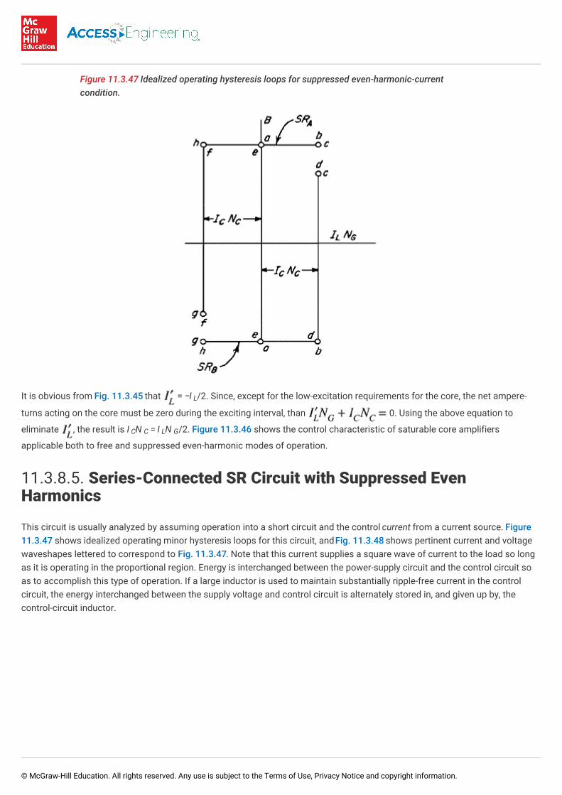
Figure 11.3.47 Idealized operating hysteresis loops for suppressed even-harmonic-currentcondition.
It is obvious from Fig. 11.3.45 that = −I /2. Since, except for the low-excitation requirements for the core, the net ampere-
turns acting on the core must be zero during the exciting interval, than 0. Using the above equation to
eliminate , the result is I N = I N /2. Figure 11.3.46 shows the control characteristic of saturable core amplifiers
applicable both to free and suppressed even-harmonic modes of operation.
11.3.8.5. Series-Connected SR Circuit with Suppressed EvenHarmonics
This circuit is usually analyzed by assuming operation into a short circuit and the control current from a current source. Figure11.3.47 shows idealized operating minor hysteresis loops for this circuit, and Fig. 11.3.48 shows pertinent current and voltagewaveshapes lettered to correspond to Fig. 11.3.47. Note that this current supplies a square wave of current to the load so longas it is operating in the proportional region. Energy is interchanged between the power-supply circuit and the control circuit soas to accomplish this type of operation. If a large inductor is used to maintain substantially ripple-free current in the controlcircuit, the energy interchanged between the supply voltage and control circuit is alternately stored in, and given up by, thecontrol-circuit inductor.
11.3.8.6. Gain and Speed of Response of SRs
L
C C L G
© McGraw-Hill Education. All rights reserved. Any use is subject to the Terms of Use, Privacy Notice and copyright information.

11.3.8.6. Gain and Speed of Response of SRs
It is obvious from the generalized control characteristic that the current gain is directly proportional to the ratio of the controlwinding turns to the gate winding turns. Thus I /I = N /N . If R is the control-circuit resistance and R is the load resistance,the power gain GP is .
The response time of saturable reactors is the combination of the time constants of the control circuit and of the gate-windingcircuit. Expressed in terms of the number of cycles of the supply frequency, the time constant of the control winding of a series-connected SR is cycles. If the SR is operating under-excited, a transportation lag may cause an
additional delay in response.
11.3.8.7. High-Performance Magnetic Amplifier (MA)
If a rectifier is placed in series with each gate winding of a parallel-connected SR and the rectifiers are poled to provide an acoutput, it becomes a type of high-gain MA circuit called the doubler circuit. When this is done, the law of equal ampere-turns nolonger applies, and the transfer characteristic is mainly determined by the magnetic properties of the SR cores. The design of anMA therefore requires more core-materials data than are required for SRs in simple magnetic amplifier circuits. The text of thissection assumes that the designer has the required magnetic-core-materials data on hand, since such data are readily availablefrom the manufacturers of cores for use in high-performance MAs.
Figure 11.3.48 Series-connected suppressed even-harmonic condition: (a) control-circuit current;(b) applied input voltage; (c) gate winding and load current; (d) voltage across series-connectedcontrol coils.
Descriptions of the operation of MAs require several terms which are defined here for reference.
Firing. In a magnetic amplifier, the transition from the unsaturated to the saturated state of the saturable reactor during theconducting or gating alternation. Firing is also used as an adjective modifying phase or time to designate when the firingoccurs.
Gate angle (firing angle). The angle at which the gate impedance changes from a high to a low value.
Gating. The function or operation of a saturable reactor or magnetic amplifier that causes it, during the first portion of theconducting alternation of the ac supply voltage, to block substantially all the supply voltage from the load and during a later
L C C G C L
© McGraw-Hill Education. All rights reserved. Any use is subject to the Terms of Use, Privacy Notice and copyright information.

portion allows substantially all the supply voltage to appear across the load. The “gate” is said to be virtually closed before firingand substantially open after firing.
Reset, degree of. The reset flux level expressed as a percentage or fraction of the reset flux level required to just prevent firing ofthe reactor in the subsequent gating alternation under given conditions.
Reset flux level. The difference in saturable-reactor core flux level between the saturation level and the level attained at the endof the resetting alternation.
Resetting (presetting). The action of changing saturable-reactor core flux level to a controlled ultimate reset level, whichdetermines the gating action of the reactor during the subsequent gating alternation. The terms resetting and presetting aresynonymous in common usage.
Resetting half cycle. The half cycle of the MA ac supply voltage at which resetting of the saturable reactor may take place.
Figure 11.3.49 Half-wave MA circuit.
Figure 11.3.50 Voltage-controlled MA circuit.
11.3.8.8. Half-Wave MA Circuits
Figure 11.3.49 shows a half-wave MA circuit with control from a source of controllable direct current. Figure 11.3.50 shows ahalf-wave MA circuit with control from a controllable source of direct voltage. The following sequence of operation is the samefor both circuits and is described in connection with Fig. 11.3.51.
1. During the gating half cycle (diode REC or REC conducting) the core flux increases toward a saturation level (3′) from somereset flux level (0) and the current to the load R is very low.
1
L
© McGraw-Hill Education. All rights reserved. Any use is subject to the Terms of Use, Privacy Notice and copyright information.

2. When saturation of the SR occurs at 2′, firing occurs and current flows to the load for the rest of the gating half cycle, leavingthe core flux at 4′.
3. During the resetting half cycle (diode REC or REC blocking) the SR core is reset from 4′ through 5′ to a value of reset fluxlevel corresponding to B′ and 0.
The waveshape of the current to the load is the same for both circuits, being a portion of one polarity of sine wave (phase-controlled half-wave). The two types of control circuits differ as follows:
Figure 11.3.51 Major and operating minor dynamic hysteresis loops for circuit of F. 11.3.49.
1. The curve on the reset portion of the hysteresis loop between 4′ and 0 is as shown in Fig. 11.3.51 for the current control typeof control circuit (Fig. 11.3.49), but for the circuit of Fig. 11.3.50, the resetting portion of the curve in the region 5′ is not avertical line and may coincide with the outer major hysteresis loop for a substantial portion of the resetting period.
2. The output of the circuit of Fig. 11.3.49 is a maximum for zero dc control current, but for Fig. 11.3.50 the output is aminimum for zero dc control voltage.
The operation of a half-wave MA can be summarized as follows: (1) During the gating half cycle, the core acts to withholdcurrent from the load for a portion of each half cycle, the length of the withholding period being determined by the degree ofreset of core flux provided during the immediately preceding resetting half cycle. (2) During the resetting half cycle, the degreeof reset can be controlled by varying the amount of direct current of proper polarity in the control winding, or by varying theamount of average voltage of proper polarity applied to the control winding. (3) The amount of current and power required toreset the core is primarily a function of the excitation requirements of the core and bears no direct relationship to the powerdelivered to the load.
1
© McGraw-Hill Education. All rights reserved. Any use is subject to the Terms of Use, Privacy Notice and copyright information.

Figure 11.3.52 Full-wave ac-output MA circuit with high-impedance control circuit.
Figure 11.3.53 Full-wave bridge MA circuit with inductive load.
11.3.8.9. Full-Wave MA Circuits
Two half-wave MA circuits can be combined to provide either full-wave ac output (Fig. 11.3.52) or full-wave dc output (Fig.11.3.53). During the gating half cycle, all gate windings act in the same manner as described for the half-wave MA circuit.Because of an interaction of the common load resistor voltage with the availability of inverse voltage across a rectifier duringits resetting half cycle, each half-wave part of Fig. 11.3.52 cannot be assumed to operate independently of its mate. Thedifferences in control characteristics are shown by Fig. 11.3.54, where curve A applies to the circuit of Fig. 11.3.49 and curve Bapplies to the circuit of Fig. 11.3.52.
11.3.8.10. Equations for MA Design
For SRs in simple MA circuits, since the ampere-turn balance rules apply, their design is so similar to transformer design thatordinary transformer design procedures are applicable. For SRs in MA circuits, the gate windings must carry rms load currentsthat are related to the ac and dc load currents in the same manner that rectifier transformer secondary rms currents are relatedto the load current. Gate windings must be able to withstand a full half cycle of ac supply voltage, without saturation, for a totalflux swing from –Bμ to + Bμ , where Bμ is the flux density at which the permeability of the core material is a maximum. Inthe cgs system of units:
Maximum ac supply voltage, rms: E = 4.44N Bμ Af × 10 , where N is gate winding turns, A is core area, and f is supplyfrequency.
m m m
e G m−8
G
© McGraw-Hill Education. All rights reserved. Any use is subject to the Terms of Use, Privacy Notice and copyright information.

Maximum load current for firing angle α = 0° (rectified average): I = E /1.11(R + R ), where R is total gate windingresistance, including diode drops, and R is the effective load resistance.
For current-controlled MA circuits the following equations apply:
Minimum load current (α = 180°); I = 2I = 2H l/0.4πN , where I = exciting current (A) of one SR core. H = sine fluxcoercive force of the core material (Oe) and l = mean length of magnetic circuit of one core.
Control current for upper end of control current: I = H l/0.4πN , where H = dc coercive force of the core material.
Control current for minimum load-current point: I = H l/0.4πN . Ampere-turn gain G = (I /2I )π.
Time constant seconds, where R is the control circuit resistance and assuming α = 90°. This
equation does not take into account a transportation or any underexcited effects which increase the delay time.
Power gain , where k = form factor (ratio of rms to average values). If only average values are
used, k is unity. At α = 90°, dynamic power gain G = G /τ = πfI R /I (R + R ) per second.
Figure 11.3.54 MA circuit control characteristics: (A) half-wave circuit; (B) full-wave ac-outputcircuit.
Figure 11.3.55 Three-legged SR core-and-coil configuration.
LM e G L G
L
LX X csf G X csf
C C C C
C csf C AT LM X
C
f
f D p C LM L X G L
© McGraw-Hill Education. All rights reserved. Any use is subject to the Terms of Use, Privacy Notice and copyright information.

Figure 11.3.56 Four-legged SR core-and-coil configuration.
For voltage-controlled MA circuits, the following equations apply to Fig. 11.3.50:
AC bias voltage E > E N /N and of indicated relative polarities. A value of E = 1.2E N /N is usually adequate. Since the
dc control voltage E acts to inhibit the resetting effect of E , a firing angle α = 0° occurs when .
A single-stage amplifier has a half-cycle transport lag and no other time delay unless the resetting is inhibited by common-loadinteractions with other half-wave-amplifier elements.
Maximum average load current I = 0.9E /(R + R ).
Minimum average load current I = I = H l/0.4πN .
The calculation of the power gain of voltage-controlled MA circuits largely depends on the control circuit. The dc control voltageof Fig. 11.3.50 actually must absorb power from the ac bias circuit during much of its control range. Assuming that E = 1.2E N/N and a resistor is connected across the control source, which has a drop of 0.2E at cutoff, then
. The maximum dc control voltage is then 1.2√2 E N /N .
When the dc control voltage, E > 2E , rectifier REC is blocking all the time, and so the only load on the control source is .
Therefore the maximum power from the control source .
The maximum power output is
The power gain is then G = P /P if the gain is assumed to be linear over most of the control characteristic. This can also be
written .
11.3.8.11. Core Configurations
Figures 11.3.55 and 11.3.56 show two coil-and-core configurations commonly used for SRs. The best core-and-coil geometryfor the SRs and MAs is the toroid-shaped core with the gate winding uniformly wound over the full 360° of the core. Full-waveoperation requires two such cores. After winding a gate winding on each core of a matched pair, the two cores and coils can bestacked together coaxially and the required control coils wound over the stack. The gate coils are so connected into the loadcircuit that no fundamental or odd-harmonic voltage is induced in the control windings.
11.4. OPERATIONAL AMPLIFIERS
11.4.1. DIRECT-COUPLED AMPLIFIERS
2 1 C G 2 1 C G
C 2
LM 1 G L
LX X csf G
2 1
C G 2
1 C G
C 2 2
p 0 C
© McGraw-Hill Education. All rights reserved. Any use is subject to the Terms of Use, Privacy Notice and copyright information.

Samuel M. Korzekwa
A direct-coupled amplifier has frequency response that starts at zero frequency (dc) and extends to some specified upper limit.To obtain the zero-frequency capability, such amplifiers are normally direct-coupled throughout; i.e., they do not use capacitiveor transformer coupling (except for auxiliary higher-frequency compensation or signal transmission).
The primary sources of error of a direct-coupled amplifier are initial offset, drift, and gain variations, errors usually dependent ontemperature, aging, and so forth. The gain-variation problem can be minimized by feedback gain-stabilization techniques, butoffset and drift errors are usually not handled so effectively by feedback techniques. A bias shift or drift error cannot bedistinguished from a signal response because their output responses are identical. Various techniques are available tominimize this drift problem, and several different methods may be used in an amplifier.
One method of minimizing drift is to use a balanced topology, as in differential amplifiers, whereby the drift errors tend tocancel out. A more complicated but effective method is the modulated-carrier-amplifier approach: the signal is first convertedinto a carrier signal, amplified using an ac-coupled amplifier, and then demodulated to a baseband signal. The functionperformed by the modulated-carrier amplifier is identical with that of a direct-coupled amplifier, but the signal processingtechnique differs.
An example of a direct-coupled transistor amplifier is illustrated in Fig. 11.4.1. The primary signal path, shown in heavy lines,directly couples the input signal to the amplifier output. This configuration also provides gain and bias stabilization via thedirect-coupled R feedback path. Usually the low-frequency amplifier voltage gain is primarily determined via the R and R components, while the function of the C capacitor and R resistor is to provide high-frequency compensation or stabilization.Sources of error for this topology include the initial V offset of the Q input transistor and the subsequent drift caused by thetemperature dependence of this offset.
11.4.1.1. Differential Amplifiers
3 1 3
1 6
BE 1
© McGraw-Hill Education. All rights reserved. Any use is subject to the Terms of Use, Privacy Notice and copyright information.

11.4.1.1. Differential Amplifiers
A differential amplifier is a dual-input amplifier that amplifies the difference between its two signal inputs. This amplifier mayhave an output that is single-ended (one output) or it may have a differential output.
The differential amplifier eliminates or greatly minimizes many common sources of error. The drift problem encountered indirect-coupled amplifiers can be handled more effectively by the differential approach. A second major advantage of adifferential amplifier is its ability to reject common-mode signals, i.e., unwanted signals present at both of the amplifier inputs orother common points. Common-mode performance is usually a critical requirement of instrumentation amplifiers.
Figure 11.4.1 Direct-coupled transistor amplifier.
The basic circuit commonly used in differential amplifiers is shown in Fig. 11.4.2. Such differential pairs can be constructedusing separate devices or in integrated-circuit form. The integrated package yields additional advantages since the parameterdifferences between the units of the integral differential pair are usually much less than if separate devices are used. Thus theunits of such integral pairs tend to track differentially more closely, even though their individual parameters may vary inabsolute value. Also, many of the passive components in the integrated amplifiers track better. Figure 11.4.3 shows a typicaldifferential transistor amplifier. For further detailed information, including analysis procedures, design techniques, andapplication data, refer to the literature.
11.4.1.2. Chopper (Modulated-Carrier) Amplifiers
The chopper amplifier performs the function of a direct-coupled amplifier by using a carrier frequency and an accoupledamplifier. The modulated-carrier approach is used specifically to minimize drift and offset types of errors. Although thisapproach is often more complex to implement, the performance improvement makes this technique desirable for applicationsdemanding low-drift performance.
© McGraw-Hill Education. All rights reserved. Any use is subject to the Terms of Use, Privacy Notice and copyright information.

Figure 11.4.2 Differential amplifier pair.
Figure 11.4.4 shows the block diagram of a modulated-carrier amplifier. While the input and output signals are dc-coupled, theinterstage coupling between the modulator, amplifier, and demodulator may be either a capacitor or a transformer.
Since modulator and demodulator are usually operated synchronously, the carrier delay must be maintained at acceptablelevels. Low-pass filters are generally included in the modulator and demodulator. The choice of carrier frequency depends onthe application. Typical examples of low-frequency carriers are 60 and 400 Hz. Carrier frequencies above 10 kHz are alsofeasible. Since the chopper and demodulator generate noise at their carrier frequency and its harmonics, the carrier frequencyshould normally be chosen above the baseband frequency range of interest. Early chopper modulators and demodulators weremechanical devices, but modern types employ solid-state electronics.
A variation of the modulated-carrier technique uses the chopper-stabilized approach illustrated in Fig. 11.4.5, which includes anadditional parallel ac-coupled high-frequency signal path. The two signal paths have gains and bandwidths tailored to acrossover frequency; e.g., when the high-frequency signal path becomes dominant, the modulated-carrier signal path ceases tocontribute to the sum total. This variation offers the low-drift advantages of the carrier-modulated system with much higherbandwidth.
Figure 11.4.3 Two-stage differential amplifier with common-mode feedback.
© McGraw-Hill Education. All rights reserved. Any use is subject to the Terms of Use, Privacy Notice and copyright information.

Figure 11.4.4 Modulated-carrier (chopper) amplifier.
Figure 11.4.5 Chopper-stabilized amplifier.
11.4.1.3. Operational Amplifiers
An operational amplifier is intended to realize specific signal processing functions. For example, the same operational amplifier(depending on the externally added components) can be used as an integrating amplifier, a differentiating amplifier, an activefilter, or an oscillator, among others. Applications of operational amplifiers also include such functions as impendancetransformers, regulators, and signal conditioning. They are versatile building blocks that can also be used in nonlinearapplications to realize functions such as logarithmic amplifiers, comparators, ideal rectifiers, and so forth.
The early application of operational amplifiers was largely in the area of analog computations. The requirements placed on theamplifiers were severe, and the cost was high. Currently, however, these high-performance functions are available at low costand are widely used.
An operational amplifier can be either direct-coupled or ac-coupled. Most operational amplifiers have differential inputs andconsequently realize common-mode rejection; however, many operational amplifiers are single-ended. Their power capabilitycovers a wide range, and they can function as a power driver. The open-loop bandwidth can range from below 1 kHz up to themegahertz range. Voltage gain can be designed from unity to above 100,000.
To design or use the many excellent models now available commercially, it is necessary to understand the attributes andlimitations of these versatile building blocks. The reader is referred to the literature and, of course, to the data sheets andapplications literature of individual suppliers of op amps.
11.4.1.4. Application of Operational Amplifiers
Figure 11.4.6 shows the block diagram for an operational amplifier with associated external elements. A represents thetransfer function of the amplifier, either current gain or voltage gain, which is generally frequency-dependent. Z and Z are theprimary elements that normally determine the closed-loop transfer function for this operational amplifier. The indicated Z andZ are equivalent summing node and load impedances, respectively, which are usually factored into the error terms of thecomposite transfer function. All the elements are general impedances that may be real or complex. Thus the simplified transferfunction of this operational amplifier can be written
1
i f
in
l
© McGraw-Hill Education. All rights reserved. Any use is subject to the Terms of Use, Privacy Notice and copyright information.

Figure 11.4.6 Operational amplifier A 1 with external impedances which determine its functionalapplication.
(1)
The error terms of the complete transfer function equation are not shown in Eq. (1); however, the complete equation with errorterms can be readily derived or obtained from the literature. Thus, if the required constraints are adhered to, Eq. (1) can be usedto generate various transfer functions, as illustrated in the examples given below.
Integrating Amplifier. An example of an integrating amplifier is shown in Fig. 11.4.7. Assume that the external-componentvalues are as indicated and that the A amplifier is a widely used commercial integrated circuit op amp. Using Laplacetransform notation, the integrator transfer function becomes
(2)
Figure 11.4.7 Operational amplifier used for integration: (a) basic schematic; (b) frequencyresponse.
Using the component values specified in the figure, the integrator transfer function can then be written
(3)
An alternative frequency-domain representation of the above integrator transfer function can also be used.
1
© McGraw-Hill Education. All rights reserved. Any use is subject to the Terms of Use, Privacy Notice and copyright information.

(4)
The closed- and open-loop frequency responses of this operational integrator amplifier are illustrated in Fig. 11.4.7b.
The frequency range of application depends primarily on the accuracy desired. In this example, 1 Hz to 10 kHz frequency isconsidered a realistic range of operation. For very low frequencies the error tends to increase because of inadequate excessgain within the operational amplifier, whereas for high frequencies the closed-loop gain becomes low and drift and offset errorsmay then become important.
Differentiating Amplifier. An example of a differentiating amplifier is shown in Fig. 11.4.8. The following simplified closed-loopequations are applicable:
(5) (6)
11.4.1.4. (7)
Figure 11.4.8 Operational amplifier used for differentiation: (a) basic schematic; (b) frequencyresponse.
The frequency responses of this operational amplifier differentiator are shown in Fig. 11.4.8b. The open-loop response of theoperational amplifier of Fig. 11.4.7 is used, and the differentiator closed-loop response is superimposed onto it.
The frequency range of this operational amplifier differentiator depends primarily on the closed-loop differentiation accuracyrequired. The difference between open- and closed-loop transfer functions (usually referred to as excess gain) can be used topredict the accuracy of the function being generated. A realistic frequency range is from 0.01 to 100 Hz. At very low frequenciesthe closed-loop gain becomes very small, and consequently errors such as drift and offset may become critical. At highfrequencies the accuracy degrades, and ultimately an integration function is generated rather than the differentiation functionintended.
11.4.1.5. Servo Amplifiers
The function of a servo amplifier, one of the principal components in a control feedback system, is to amplify the input (usuallylow-level) error signals and to provide rated drive power to the load (the servo actuator). Servo amplifiers can be dc- or ac-operated, and can be linear or nonlinear.
Direct-Coupled Servo Amplifiers. A direct-coupled servo amplifier can operate on dc error signals, i.e., zero frequency signals.The bandwidth of a dc servo amplifier is often quite large, and thus it has the capability of dynamic operation. In practice it isoften operated in the dynamic mode, and the transient-response characterization is often used.
© McGraw-Hill Education. All rights reserved. Any use is subject to the Terms of Use, Privacy Notice and copyright information.

A servo amplifier is intended to drive or control its load to some prescribed reference level. It is the drift and offset errorsassociated with this control function that are the main concern in this dc mode of operation. Thus, if the actuator is positionedat its exact reference level, the amplifier should provide zero drive power. However, because of initial offsets or subsequenttemperature or aging effects, the amplifier may still provide unwanted drive to the load. The usual solution is to minimize theseproblems by circuit design, e.g., tracking or balanced configurations, or by use of an intermediate-carrier modulated by the dcerror input signals, subsequently demodulated for use as the direct-coupled drive to the actuator.
AC Servo Amplifiers. An ac servo amplifier operates at a selected fixed frequency and is consequently a carrier-systemamplifier. The most commonly used carrier frequencies are 60 and 400 Hz, but ac servo systems can be designed to operate atalmost any frequency compatible with the servo actuator used.
The principal advantage of ac servo amplifiers is that the previously discussed drift and offset problems present in dc servoamplifiers are virtually eliminated. Another advantage is that the prime power from the actuator now can be supplied directlyfrom the line, for example, 60-Hz 115-V source.
For applications wherein the servo actuator or load is a servomotor, the load is often tuned to the carrier frequency via theaddition of a capacitor in parallel with the motor. Note that the servomotor impedance is a function of the motor speed;however, the losses (usually resistive) change, whereas the parallel inductance remains virtually constant. Thus tuning the loadcauses it to become real (resistive), and consequently the efficiency of the amplifier output stage improves significantly.
The output stage of an ac servo amplifier is usually operated class B or AB and in a push-pull configuration to obtain the bestpossible drive efficiency. Figure 11.4.9 shows an example of a push-pull tuned-load ac servo amplifier.
Nonlinear Servo Amplifiers. This class of servo amplifier uses the load to filter the highly nonlinear drive signals resulting inimproved drive efficiencies and higher realizable driver-power capabilities. The drivers essentially act as switches wherein thedissipation losses are low when the switches are either on or off. Since the loads or servo actuators are usually highly reactive,they can be advantageously used in this manner. The drive power can be readily derived from a dc source via a pulse-width-modulated scheme. In addition, an ac source of power can also be used via a phase-modulation technique. Some examples ofhigh-power switching devices used for ac nonlinear servo amplifiers are thyratrons and silicon controlled rectifiers (SCRs).
Figure 11.4.9 Servo amplifier used as a motor drive.
11.4.2. OPERATIONAL AMPLIFIERS FOR ANALOGARITHMETIC
© McGraw-Hill Education. All rights reserved. Any use is subject to the Terms of Use, Privacy Notice and copyright information.

Joseph P. Hesler
11.4.2.1. Analog Multiplier Circuits
Circuits used for analog multiplication fall into three categories: transconductance multipliers, averaging-type multipliers, andexponential multipliers.
11.4.2.2. Transconductance Multipliers
The most prominent type of transconductance multiplier uses the property of the bipolar transistor; i.e., its collector current andtransconductance are linearly related. The balanced transistor differential amplifier used in these circuits offers good accuracy,wide bandwidth, and low cost.
Figure 11.4.10 Basic differential amplifier for analog multiplication.
In the differential amplifier as shown in Fig. 11.4.10, the collector currents I and I are functions of the differential inputvoltage V − V . It is assumed that the current transfer ratios of the two transistors (Q and Q ), the junction ambienttemperatures, and the base-emitter junction saturation currents are the same, as is probable in integrated-circuit fabrication.
The diode equation governs the relationship between the transistor emitter currents I and the base-to-emitter voltage V
c 1 c 2
b 1 b 2 1 2
Ei BE 1
© McGraw-Hill Education. All rights reserved. Any use is subject to the Terms of Use, Privacy Notice and copyright information.

Figure 11.4.11 Transfer curves on which analog multiplication is based.
where I = junction saturation current
q = electron charge = 1.6 × 10 C
k = Boltzmann’s constant = 1.38 × 10 W/s·K
T = junction temperature (K)
The relationships of collector currents, shown graphically in Fig. 11.4.11 are
For zero differential input, and α = α , and so
At zero input, ΔV = 0, the maximum single-ended transconductance occurs at
For a differential output connection the maximum transconductance is twice this value. The linear range of transconductanceextends over a differential input signal range of about 50 mV peak to peak at room temperature.
S
19
–23
1 2
BE
© McGraw-Hill Education. All rights reserved. Any use is subject to the Terms of Use, Privacy Notice and copyright information.

Figure 11.4.12 Four-quadrant transconductance multiplier.
Linear multiplication occurs when one input varies the I term and the other input is used to vary ΔV .
The linear range of input voltage can be extended by inserting resistance in series with each emitter. This increase in allowablesignal is accompanied by a corresponding reduction in transconductance. For I equal to 2 mA, the addition of 50 X in serieswith each emitter increases the linear input swing by a factor of 3 and reduces the transconductance to one-third. Optimizationof the transconductance multiplier operation requires a trade-off between linearity and error sources because of offset voltagesand thermal noise.
A typical four-quadrant multiplier using the differential amplifier as building blocks is shown in Fig. 11.4.12. This circuit isgenerally used with differential inputs to obtain maximum linearity and common-mode signal rejection.
Figure 11.4.13 Block diagram of an averaging-type multiplier.
11.4.2.3. Averaging-Type Multipliers
0 BE
0
© McGraw-Hill Education. All rights reserved. Any use is subject to the Terms of Use, Privacy Notice and copyright information.

11.4.2.3. Averaging-Type Multipliers
Two types of averaging multipliers have found extensive use. The first type, the pulse height and width multiplier, uses one ofthe input variables to modulate the height or amplitude of a pulse train, while the pulse width is modulated with the other inputvariable. The pulse area, averaged over a suitable period, is proportional to the product of the input variables. High pulse ratespermit short averaging intervals and fast response. These multipliers offer very good accuracy and stability but are moreexpensive than the transconductance multipliers. A block diagram of a typical pulse height and width averaging multiplier isshown in Fig. 11.4.13.
A second version of the averaging multiplier is the triangle averaging multiplier. In this type a high-frequency triangularwaveform is generated and combined with the input variables to form an averaged output proportional to the product of theinput signals. These multipliers are less accurate than the pulse height and width multipliers and are being displaced bytransconductance multipliers.
A third type of averaging multiplier is the time-base multiplier. This approach uses a comparator to sense the time intervalrequired for the integral of a reference input voltage to equal the amplitude of a sample of one input variable. During the sameinterval, 0 to T, the other input variable is integrated to produce an output V. This type of circuit can be built with a fewcomponents to provide moderate accuracy, 1 to 5 percent, at low cost.
11.4.2.4. Exponential Multipliers
The first electronic multipliers were of the exponential type. In these circuits, resistor-diode networks are designed to provide acurrent or voltage output approximating the square of the input. These multipliers are also called quarter-square multipliersbased on the identity
The piecewise-linear approximations to the squared response result in “lumpy” error characteristics. Also, the amount ofcircuitry required to compute the quarter-square algorithm is expensive. Although these multipliers are capable of goodaccuracy and bandwidth, they are becoming obsolete.
A second type of exponential multiplier uses logarithmic amplifiers, a summer, and an antilog amplifier to implement therelationship
Semiconductor diodes are available with excellent logging characteristics over many decades of bias current. These diodes areused with operational amplifiers to realize the necessary functions. The circuits can provide moderate to good accuracy (withthermal compensation) and good bandwidth. Applications are restricted by unipolar input requirements and differential driftbecause of thermal effects.
11.4.2.5. Multiplier Error Sources
© McGraw-Hill Education. All rights reserved. Any use is subject to the Terms of Use, Privacy Notice and copyright information.
11.4.2.5. Multiplier Error Sources
Offset Error. There are two subclasses of offset error. The first is static offset caused by variances in component parameterssuch as saturation current I , in transistors and diodes. The second error is a result of drift in component parameters. While theinitial static offset can be trimmed with external adjustments, the drift components must be compensated by introducingcomplementary temperature coefficients within the circuit. A common source of drift is local heating of diode junctions andresistive components having nonzero temperature coefficients.
Feedthrough Error. Feedthrough errors result from nonideal transfer characteristics. Two feedthrough error contributions canexist. The first, E , is defined as the output owing to the input variable Y when the X input is zero. The second, E , is thecomplementary function owing to an X input. Feedthrough erros may result in dc, fundamental, and harmonic components ofthe contributing input signal.
Gain and nonlinearity errors. Gain errors produce output deviations from the expected scale factor of the multipliers.Nonlinearity of the transfer functions of the multiplier can produce additional error contributions, as previously discussed. Gainis most apt to vary as a function of the combined input-signal values because the internal components are operated over arange of bias conditions.
In certain multiplier applications, required transient responses may overtax the bandwidth capabilities of the circuits. In theseinstances additional error terms may appear as a result of limited slew rate of the circuits and differential phase responsebetween the input channels.
11.4.2.6. Squaring Circuits
Squaring circuits are readily implemented by introducing the variable to both inputs of a multiplier circuit. Alternatively, theresistor-diode squaring circuits used in exponential multipliers may be applied directly.
11.4.2.7. Dividing and Square-Root Circuits
s
FY FX
© McGraw-Hill Education. All rights reserved. Any use is subject to the Terms of Use, Privacy Notice and copyright information.

11.4.2.7. Dividing and Square-Root Circuits
Division and square-root functions can be implemented with basic multiplier circuits by altering the interconnections. A typicaldividing-circuit connection is shown in Fig. 11.4.14. The multiplier output is fed back through a summing amplifier to one of themultiplier inputs. The summing amplifier maintains an equivalence between the numerator Y and the multiplier output XE /K.
Figure 11.4.14 Dividing circuit.
Figure 11.4.15 Square-root circuit.
Square-root circuits can be implemented in a similar method with another feedback connection involving a multiplier. In thisinstance, the output is used as each of the two multiplier-input variables, and the multiplier output is summed with the variablewhose square root is desired. The square-root connection is shown in Fig. 11.4.15. The nonnegative input limitations should bestated for division and square-root connections.
11.4.3. LOW-NOISE OPERATIONAL AMPLIFIERS
Clayton R. Roberts
11.4.3.1. Low-Noise Op-Amp Design
0
© McGraw-Hill Education. All rights reserved. Any use is subject to the Terms of Use, Privacy Notice and copyright information.

11.4.3.1. Low-Noise Op-Amp Design
The use of the standard operational-amplifier module or chip has grown into many areas of design because of its low cost,ease of design, and low number of supporting components. Some of the well-known basic amplifier uses are shown in Fig.11.4.16. Low-noise amplifier developments have moved into the op-amp category for the same reasons. Applications in thisarea include microphone pre-amplifiers, threshold detectors, instrumentation amplifiers, and sensor amplifiers. Good low-noiseop-amps are available, and understanding some of the basic design principles is helpful when using them.
Figure 11.4.16 Basic operational-amplifier configurations.
There are many types of noise derived from a number of sources, but the types concerning amplifiers include 1/f or pink noiseand thermal and other current-and voltage-associated effects within the amplifier. Pink noise is of concern at the very low endof the spectrum and involves dc amplifiers and some types of sensors. Generally the amplifier noise density can be expressedas follows:
where e = p-amp noise voltage
i = op-amp current noise
R = equivalent input source resistance (including
feedback network)
e = thermal noise of source network (resistance)
n
n
eq
t
© McGraw-Hill Education. All rights reserved. Any use is subject to the Terms of Use, Privacy Notice and copyright information.

and since
where K = 1.38 × 10 , T = 300 K, then
Figure 11.4.17 Simple op-amp configuration with and without bias.
–23
© McGraw-Hill Education. All rights reserved. Any use is subject to the Terms of Use, Privacy Notice and copyright information.

Figure 11.4.18 Voltage and current noise characteristics of a commercially available op amp.
The R can become a predominant influence in the noise of the amplifier. This resistance is the combination of the resistivecomponent of the input to the amplifier and the feedback network. It is obvious that the input to the amplifier should be kept aslow as possible without loading down the device the amplifier is attached to. Figure 11.4.17 shows the R of the simpleamplifier. When offset bias is added to the op amp, the thermal and current noise components must be added to the noiseequation. Usually the bias resistance is equal to the R making the noise density
The amplifier design should have bandwidth restrictions on it so that the band extent does not go beyond that which isnecessary. When the amplifier design is the first stage of a larger amplifier and it becomes the noise determining circuit, thebandpass restrictions do not have to be repeated further on.
There is one other consideration regarding the R and the source resistances. If truly low noise is desired, noncarbon resistorsare needed in this part of the circuit. Metal film resistors are best. Wire-would resistors are also a possibility, but not if highfrequencies are involved. Carbon resistors have a larger “particle component” of noise beside the normal thermal noise.
Generally, the current noise i and voltage noise e remain relatively constant above 1 kHz and rise somewhat below 100 Hz,as shown in Fig. 11.4.18. If high values of R or source resistances are necessary, op-amp selection is possible to reducenoise in parts of the spectrum. This is apparently a result of the biasing arrangement of different op amps with their inputtransistors . With R less than 1 kΩ, the thermal noise is expected to be low and the total noise is
dominated by the voltage noise e .
11.4.4. POWER OPERATIONAL AMPLIFIERS
Clayton R. Roberts
11.4.4.1. Power Op Amps
eq
eq
eq
eq
n n
eq
eq
n
© McGraw-Hill Education. All rights reserved. Any use is subject to the Terms of Use, Privacy Notice and copyright information.

The advent of the power op amp has provided us with another versatile design approach when high-current high-voltage driverequirements are needed. It is useful in motor drive circuits, deflection sweep circuits, many control functions, and high-qualityaudio amplifiers. Distortion levels below 0.05 percent can be achieved. In addition to the high-voltage high-current ratings thepower op amps usually provide better matched components from internal control of the devices and laser trimming of thestages. Standard design approaches for op amps are used except for some considerations mentioned below. The definition ofwhere the power op amp takes over from the standard op amp appears to be when the total supply voltage must be above 44 Vand the delivered current is above 0.1 A.
Power Dissipation. In addition to the maximum voltage rating concerns, the power op-amp design must include operatingtemperature and dissipation values. Mounting of the device as well as the operating region of the parameters is a major designcriterion. Figure 11.4.19 shows the effect of junction temperature of the power devices on failure rates as was derived from thebase failure rate tables of MIL-HDBK-217C. Some power op-amp manufacturers design the cases so that they can be directlymounted to grounded heat sinks so that there is minimum thermal resistance to the sink. The required thermal resistance from a heat sink is calculated by the following:
where T = maximum junction temperature
T = maximum ambient temperature
P = internal power dissipation
= thermal resistance of the amplifier
Another heat-sink-design approach (Fig. 11.4.20) offers the approximate area required of a convection cooled surface.
The complexity of the power-dissipation calculation is very much dependent on the type of load that is being driven. Taking dcor instantaneous values of current and voltage, it may be expressed as
Figure 11.4.19 Failure rate (MTTF) vs. junction temperature.
j
a
dis
© McGraw-Hill Education. All rights reserved. Any use is subject to the Terms of Use, Privacy Notice and copyright information.

Figure 11.4.20 Heat-sink area estimated for temperature rise and several values of powerdissipation.
Figure 11.4.21 Safe operating curves for a power operational amplifier.
where V = one rail of the supply voltage
V = output voltage
I = output current
V = rail-to-rail supply voltage
I = quiescent current
For sinusoidal waveforms the peak value of P may be expressed as
where θ is the absolute value of the phase angle of Z and Z is the magnitude of the load impedance. This function isapproximate.
s
o
o
ss
q
dis
l
© McGraw-Hill Education. All rights reserved. Any use is subject to the Terms of Use, Privacy Notice and copyright information.

Safe-operating-area (SOA) curves are supplied by some manufacturers to aid in limiting the power dissipation to withinspecifications. Figure 11.4.21 shows a curve for a commercial power op amp. The secondary breakdown region shown resultsfrom excess current densities in the base region of the output devices when high collector current occurs simultaneously withhigh collector-emitter voltage. These curves include all contributors to the dissipation problem. The three curves at the right-hand end of Fig. 11.4.21 are the limits of the short-pulse power applications for the SOA curve. Pulse width values of 0.5, 1.0,and 5.0 ms are indicated. Additional foldover or limiting current protection can be obtained when operating near the limits (rail)(refer to manufacturers product data).
Output Loads. Output loads can have reactance components involved even if they are designed to be resistive. With the highercurrents present, and especially transients, reactive, or flyback (reversed polarity) voltages can exceed specified limits. Mostpower op amps have built-in diodes between the two rails and the output to help suppress such transients. By necessity thesecan handle limited current. Several manufacturers recommend external diodes be placed between the output of the op amp andeach of the supplies. The back emf must be considered in the design (SOA curves). This is especially true with loads such asmotors. Start-up and reverse conditions must be accounted for. Some types of loudspeaker circuits present a similar situation.
Circuit Layout. Lead inductance must be kept to a minimum. This is sometimes taken care of by use of a microstrip-type low-impedance line approach. Power-supply transients are reduced to a minimum by bypassing right at the op amp as well as at thesupply terminals. With high currents involved, bypass capacitors must have low reactance leads and several times their normalvalues. With low-distortion amplifiers, deteriorization at the high-frequency end of the spectrum (higher distortion) can be theresult of insufficient effective bypassing from the supply sources, but this is best taken care of by large short-lead bypasses atthe device location. Ground loops and ground return interaction effects are also emphasized with the high-current devices.Input-output ground return coupling is to be avoided.
Figure 11.4.22 National Semiconductor LM12 power amplifier.
An audio power amplifier shown in Fig. 11.4.22 has some of the features indicated in a low-cost high-performance design. TheLM12 (National Semiconductor) is a 150-W op amp capable of delivering that power to a 4-Ω load. The design includesMotorola MR752 diodes in its output to the rails. These diodes are capable of handling up to 400 A of surge current, 28 Aaverage forward current, and a repetitive reverse voltage of 200 V. These specifications provide good protection againsttransients and back emf. The small capacitor in the feedback network aids in reducing the distortion at the high end of thespectrum and provides stability. The distortion is claimed to be about 0.01 percent. Good supply bypassing is obtained right atthe device terminals. A central grounding point is used to avoid ground coupling of output to input. Thermal limiting, outputcurrent limiting, and over voltage shutdown is designed into the device. Note the parts count associated with circuit.
11.5. HIGH-POWER AMPLIFIERS
11.5.1. THERMAL CONSIDERATIONS
© McGraw-Hill Education. All rights reserved. Any use is subject to the Terms of Use, Privacy Notice and copyright information.

11.5.1. THERMAL CONSIDERATIONS
A problem common to all high-power amplifier and oscillator equipment is removal of the excess thermal energy produced inthe active devices and other circuit components so that operating temperatures consistent with reliable performance can bemaintained. Available cooling methods are radiation, natural convection, forced convection, liquid, evaporative, and conduction.Radiation and evaporative cooling depend for suitable operation on a rather high temperature for the device being cooled andare thus generally restricted to use with vacuum tubes. The remaining methods are suitable for use in both solid-state andvacuum-tube systems.
11.5.2. HIGH-POWER BROADCAST-SERVICE AMPLIFIERS
Transmitters for amplitude modulation broadcast service may employ high-level (plate) modulation or low-level (grid or screen)modulation of the output stage or modulation of an intermediate stage, followed by linear amplification in the followingstage(s). Generally, the last approach is used in very-high-power transmitters, because of the difficulty and expense in designingand building a modulation transformer to handle the high audio modulating power required. High-level modulation has beenused in AM transmitters up to at least 250 kW carrier power with a modulator output power requirement of 125 kW. By a uniquedesign in which the positive terminal of the modulator plate supply is grounded, and autotransformer is used as the modulationtransformer, with a significant reduction in size and cost.
11.5.3. CLASS B LINEAR RF AMPLIFIERS
The conventional means for achieving linear amplification of an AM signal is the class B rf amplifier circuit, often referred tosimply as a linear amplifier. The plate efficiency, plate dissipation, and output power are highly dependent on the drive level. It isconvenient, therefore, to define a drive ratio or normalized drive level k.
where E is the dc plate supply voltage and E is the peak ac plate signal voltage.
Class B amplifiers using transistors can approach the theoretical maximum collector efficiency of π/4, or 78.54 percent, as aconsequence of the very low collector saturation voltage of transistors, which gives a correspondingly high value for K.
11.5.4. HIGH-EFFICIENCY POWER AMPLIFIERS
The plate efficiency at carrier level in a practical linear amplifier circuit is about 33 percent, while that of a high-level (plate)modulated stage is 65 to 80 percent. When the efficiency of the modulator is taken into account, the net efficiency of the high-level modulated stage is still higher than that of the linear amplifier, since the output power level of the modulator is at mostone-third of the total output power of the modulated stage.
Because of the difficulty and expense involved in the design and manufacture of very large modulation transformers andchokes, several linear amplifier circuits having much greater efficiency than the class B amplifier while amplifying an AMwaveform have been developed. Low-level modulation can be employed, and the need for the large, expensive modulatorcomponents is circumvented.
Such high-efficiency amplifier circuits include the Chireix outphasing modulated amplifier, the Dome high-efficiency modulatedamplifier, the Doherty high-efficiency amplifier, and the Terman-Woodyard high-efficiency modulated amplifier.
bb pm
© McGraw-Hill Education. All rights reserved. Any use is subject to the Terms of Use, Privacy Notice and copyright information.

11.5.5. INDUCTION HEATING CIRCUITS
Induction heating is achieved by placing a coil carrying alternating current adjacent to a metal workpiece so that the magneticflux produced by the current in the coil induces a voltage in the workpiece, which produces the necessary current flow.
Power sources for induction heating, in addition to direct use of commercial power, include spark-gap converters, motor-generator sets, vacuum-tube oscillators, and inverters. Motor-generator sets generally provide outputs from 1 kW to more than1 MW and from 1 to 10 kHz. Spark-gap converters are generally used for the frequency range from 20 to 400 kHz and provideoutput power levels up to 20 kW. Vacuum-tube oscillators operate at frequencies from 3 kHz to several MHz and provideoutput levels from less than 1 kW to hundreds of kilowatts. Inverters using mercury-arc tubes have been used up to about 3kHz. Solid-state inverters operate at frequencies up to about 10 kHz and at power levels of several megawatts. These solid-state inverters generally employ thyristors (silicon controlled rectifiers) and are replacing motor-generator sets and mercury-arcinverters.
11.5.6. DIELECTRIC HEATING
Whereas induction heating is used to heat materials which are electrical conductors, dielectric heating is used to heatnonconductors or dielectric materials. The basic arrangement for a dielectric heating system is that of a capacitor in which thematerial to be heated forms the dielectric or insulator. The heat generated in the material is proportional to the loss factor,which is the product of the dielectric constant and the power factor. Because the power factor of most dielectric materials isquite low at low frequencies, the range of frequencies employed for dielectric heating is higher than for induction heating,extending from a few megahertz to a few gigahertz.
The power generated in a material is given by
where V = voltage across material (V)
f = frequency of power source (MHz)
A = area of material (in )
K = dielectric constant
t = material thickness (in)
= power factor of dielectric material
The voltage that can be applied to a particular material is limited by the insulation properties of the material at the requiredprocess temperature. The frequency that can be used is limited by voltage standing waves on the electrodes, which will beappreciable when the electrode dimensions are comparable with one-eighth wavelength (10 percent voltage variation).
11.5.7. TRANSISTORS IN HIGH-POWER AMPLIFIERS
2
© McGraw-Hill Education. All rights reserved. Any use is subject to the Terms of Use, Privacy Notice and copyright information.

Many high-power amplifier circuits can be implemented by using solid-state power devices. Bipolar transistors have beensuccessfully applied in induction heaters, sonar transmitters, and broadcast transmitters. The sonar transmitters haveemployed class B, class C, and the so-called class D power amplifier circuits. In the class D circuit the active device is used asan on-off switch, and output power variations are achieved by pulse-width modulation or supply-voltage control. A tuned load orone incorporating a low-pass filter is used with the class D amplifier.
Power MOSFETs are advantageous compared with bipolar transistors in a number of applications. These include HF and VHFtransmitters, high-speed power switching, and certain audio or low-frequency amplifiers.
The power MOSFET is a majority carrier device (contrast with a minority carrier device for the bipolar transistor). The input drivecircuit requires current to supply the parasitic capacitances only. There is no minority carrier storage time or secondarybreakdown. Switching time is usually much less than that of the bipolar transistor of the same die. The power MOSFET deviceuses a gate voltage-controlled circuit and requires very little current to maintain it in its OFF, ON, or an intermediate state. TheON resistance (r ) can vary from less than 0.5 Ω to several ohms depending on the device selected. There is a trade-offbetween high-breakdown drain-source voltage and low ON-resistance. For a given die size the ON-resistance varies as follows:
where K is a constant related to the die and V is the maximum breakdown voltage between drain and source. A typical draincurrent (I )-drain-source voltage (V ) transfer characteristic curve of a TMOS power MOSFET is shown in Fig. 11.5.1. The ON-resistance r is, of course, a function of the conduction state of the device and does have a threshold value depending on thegate voltage which controls the conduction (see Fig. 11.5.2). Also, if the design is dependent on the r value, one must keep inmind a potential shortcoming which is its variation with temperature. Figure 11.5.3 shows this function with a MotorolaMTM8N15. Temperature coefficients are provided as a function of I with a number of device data sheets. Switching speeds ofthis device are not influenced by temperature.
Considerations for Broadcast Transmitters. There are some advantages to using the power FET in this type of applicationthrough the VHF spectrum. The power FET offers stability in the drive circuit as well as its own transfer characteristics. With thebipolar transistor there is a dependent relationship between the collector current i and the current gain β. If the drive level isdecreased, causing the i to decrease, the β will increase and can cause instability in an amplifier. The input impedance canalso change as the drive level is changed. Both of these factors can become a stability design problem. The input and outputimpedances of the device are reasonably independent of drive. The input impedance is somewhat higher in magnitude andmore capacitive than bipolar devices, allowing simpler matching circuits to be used.
Figure 11.5.1 Typical on-region transfer characteristics for the MTP 7N05.06. Copyright byMotorola, Inc. Used by permission.
DS
DS
D DS
DS
DS
D
C
C
© McGraw-Hill Education. All rights reserved. Any use is subject to the Terms of Use, Privacy Notice and copyright information.

Figure 11.5.2 Variation of r DS with V GS and I D for MTP8N15. Copyrigth by Motorola, Inc. Used bypermission.
Figure 11.5.3 Variation of r DS with drain current and temperature for MTM8N15. Copyrigth byMotorola, Inc. Used by permission.
© McGraw-Hill Education. All rights reserved. Any use is subject to the Terms of Use, Privacy Notice and copyright information.

Figure 11.5.4 Power amplifier for Nautel broadcast transmitter.
There are a number of approaches used in transmitter design. Which one to use depends on the number of modulation andcarrier uses. Usually, a slightly positive (adjustable) bias is required on the gate unless strictly class C is needed. The amplifierdesign can be made to withstand high VSWR conditions in the output without damage. This is accomplished by selection of thedevice so that maximum rated drain-source voltage (V ) is not exceeded. Likewise, the gate-to-source voltage (V )cannot be exceeded. This is sometimes protected using a zener diode across the gate to source. Remember that using suchdevices tends to generate undesirable harmonics when the drive signal is clipped and a low-pass filter or equivalent is requiredin the output.
While power FET amplifiers can be operated in class A, B, AB, and C, it is of strong interest to consider class D for AMbroadcast service. Power FETs can have a wide linear operating range and swinging them hard to an ON condition allows theefficiency to be quite high. Nautical Electronic Laboratories Limited of Nova Scotia has developed a very efficient AMtransmitter using power FETs as switches (class D operation). Figure 11.5.4 shows the basic configuration of the final rfamplifier. A low-power rf drive signal at the carrier frequency is applied via T2 to bias FET pairs Q1/Q3 and commutatedbetween input terminals of T2 as a square wave of reversing polarity at the carrier frequency. The resulting high-power signal atT2 is filtered by low-pass filter F1 to remove unwanted harmonics. The final rf amplifier is thus simply a device that convertsfrom dc to rf. Efficiencies of greater than 90 percent are achievable.
The pulse width modulator also uses FETs in a switched mode to vary the negative supply to the rf power amplifier in sympathywith an audio modulating signal to produce high level modulation with a similar high efficiency. Nautical ElectronicLaboratories has developed a 50-kW solid-state transmitter of this type with distortion typically less than 1.0 percent.
11.5.8. MOSFET AUDIO AMPLIFIERS AND SWITCHING
(BR)DSS GS
© McGraw-Hill Education. All rights reserved. Any use is subject to the Terms of Use, Privacy Notice and copyright information.

11.5.8. MOSFET AUDIO AMPLIFIERS AND SWITCHINGAPPLICATIONS
The power MOSFET offers a very linear transfer characteristic. This can be used effectively with the design of audio poweramplifiers with proper gate biasing.
The gain characteristic is identified with the transconductance of the MOSFET. The voltage gain is as follows:
where g is the transconductance and R is the equivalent load. The transconductance is defined as the ratio of the change indrain current relating to a change in gate voltage. This rating on a device is typically taken at half the rated continuous draincurrent at a V of 15 V. The linear increase in g with V occurs in the square law region but levels off to a constant in thevelocity-saturated region.
Figure 11.5.5 Class D audio amplifier using power MOSFET.
Considering the very high switching efficiency the power MOSFET has, it can be effectively used as a “class D” audio amplifieror one that is pulse-width modulated at the audio rate. A high-frequency carrier is used which is on the order of 6 to 10 timesthe highest audio-modulated frequency. The waveform is demodulated at the output for driving large speaker systems. Veryhigh audio power amplifiers can be designed with high fidelity, small size, and high efficiency. Power FETs can be placed inparallel with few problems of current sharing. Figure 11.5.5 shows a simple version of this approach. With the high carrierfrequency, coupling capacitors and supply decoupling become much less severe.
fs L
gs fs gs
© McGraw-Hill Education. All rights reserved. Any use is subject to the Terms of Use, Privacy Notice and copyright information.

11.6. MICROWAVE AMPLIFIERS AND OSCILLATORS
11.6.1. MICROWAVE SOLID-STATE DEVICES
Since the 1950s, solid-state devices have replaced tubes in most amplifier and oscillator applications. Solid-state devices arepreferred because of better long-term reliability, lower cost, and improved noise characteristics. In the 1960s and 1970s,avalanche and Gunn diodes were used extensively in the generation of microwave power.
More recently, junction and field-effect transistors have been increasingly used in microwave amplifiers and oscillators. Galliumarsenide (GaAs) FETs have replaced other solid-state devices in many microwave applications; however, impact ionizationavalanche transit-time (IMPATT) and Gunn diodes are still commonly used at frequencies above 20 GHz.
11.6.2. IMPATT DIODE CIRCUITS
The generation of microwave power in a reverse-biased pn junction was originally suggested by Read (1958). He proposed thatthe finite delay between applied rf voltage and the current generated by avalanche breakdown, with the subsequent drift of thegenerated carriers through the depletion layer of the junction, would lead to negative resistance at microwave frequencies. Thediode is biased in the avalanche-breakdown region. As the rf voltage rises above the dc breakdown voltage during the positivehalf cycle, excess charge builds up in the avalanche region, reaching a peak when the rf voltage is zero. Hence this chargewaveform lags the rf voltage by 90°. Subsequently, the direction of the field in the diode causes the multiplied carriers to driftacross the depletion region. This, in turn, induces a positive current in the external circuit while the diode rf voltage is goingthrough its negative half cycle. This is equivalent to negative resistance, which is maximum when the transit angle isapproximately 0.74π.
A simplified equivalent circuit of the IMPATT diode circuit is shown in Fig. 11.6.1. The resistance R includes both the parasiticpositive resistance because of contacts, bulk material, and so forth, and the dynamic negative resistance. The net magnitude istypically in the range –0.5 to –4.0 Ω and varies with current. The capacitance C is the voltage-sensitive depletion-layercapacitance and can be approximated sufficiently accurately with the value at breakdown. The diode resistance variationresults in a stable operating point for any positive load resistance equal to or less than the diode’s peak negative value.
Oscillations will build up and be maintained at the frequency for which the net inductive reactance of the package parasitics andthe external load equals the capacitive reactance of C . The values for L and C vary with package or mounting style. Typicalvalues range from 0.3 to 0.6 nH and 0.2 to 0.4 pF, respectively. It is important to minimize these parasitics since they limit theoperating frequency and band-width.
IMPATT diodes can be used in several mounting configurations, including coaxial, waveguide, strip-line, or microstrip. It isimportant to ensure that a good heat flow path is provided (owing to the typically low efficiency) and that low-electrical-resistance contacts be made to both anode and cathode.
D
D
D P P
© McGraw-Hill Education. All rights reserved. Any use is subject to the Terms of Use, Privacy Notice and copyright information.

Figure 11.6.1 Approximate rf equivalent circuit of IMPATT oscillator.
In avalanche breakdown, the diode tends to look like a voltage source. Hence a current source is desirable for dc bias. Severalcircuits are possible. The RC bias circuit (Fig. 11.6.2a) is the simplest but is inefficient, and the transistor current regulator (Fig.11.6.2b) may be more desirable. In either case, the loading of the diode with shunt capacitance or a resonance path to ground(at some frequency) must be avoided to prevent instabilities (noise and/or spurious frequencies).
Two broadly tunable diode loading circuits are the multiple-slug cavity and the variable-package-inductance types. Coaxialimplementations of these two techniques are shown in the cross sections of Fig. 11.6.3. In Fig. 11.6.3a slugs λ/8 and/or λ/4long at the desired center frequency of operation with characteristic impedance of between 10 and 20 Ω are adjusted inposition along the centerlines to provide a load reactance equal to the negative of the diode reactance and a load resistanceequal to or less than the magnitude of the diode net negative resistance. Circuit b tunes the diode by recessing it into the holder,effectively decreasing the net series inductance, which is resonant with the diode capacitance. Single- or multisectiontransformers can also be included for resistive matching to the load R . Similar waveguide-circuit implementations can be usedwith typically narrower bandwidths, better frequency stability, and lower FM noise.
The IMPATT diode can function as an amplifier if the load resistance presented to it is larger in magnitude than the negativeresistance of the diode. Typically, a circulator is used in conjunction with the tuned diode circuit to separate input and outputsignals. At the center frequency, the power gain of the amplifier is given by
where R and R are as shown in Fig. 11.6.1.
In general, amplifier operation for a given diode requires a smaller shunt tuning capacitor or a large transformer characteristicimpedance. An estimate of the diode rf current and voltage can be obtained from
L
D L
© McGraw-Hill Education. All rights reserved. Any use is subject to the Terms of Use, Privacy Notice and copyright information.

Figure 11.6.2 Bias circuits for IMPATT diodes: (a) RC type; (b) transistor-regulated type.
Figure 11.6.3 Mechanical tuning of IMPATT circuit: (a) multiple-slug type; (b) variable-inductance(diode-recess) type. (Hewlett-Packard Company.)
where V = diode breakdown voltage
C = junction capacitance
P = power output
G = gain
Higher output powers have been achieved by multiple-diode series-parallel configurations and/or hybrid combining techniques.
In general, properly designed IMPATT oscillator circuits can have noise performance comparable with reflex klystron or Gunnoscillators. The noise performance of both Si and GaAs IMPATT diode amplifiers and oscillators has been extensively treated inthe literature.
IMPATT diodes are usable at higher frequencies than any other solid-state device currently available. Silicon IMPATT diodescan be used at frequencies as high as 300 GHz. Some of the disadvantages of IMPATTS are a low gain-bandwidth product,difficult adjustments necessary for long-term performance reliability, bias circuit instabilities, and inherent nonlinearity. The cwpower output achievable with a single
b
j
o
0
© McGraw-Hill Education. All rights reserved. Any use is subject to the Terms of Use, Privacy Notice and copyright information.

Figure 11.6.4 Typical TRAPATT diode circuit configuration.
IMPATT diode is 3 W at 11 GHz, 2 W at 15 GHz, or 1 W at 20 GHz. Diodes can be paralleled to obtain higher power, for example,10 W at 41 GHz, with 30 dB gain and 250 MHz bandwidth, by combining 12 diodes in one cavity.
11.6.3. TRAPATT DIODE CIRCUITS
The trapped plasma avalanche triggered transit (TRAPATT) mode of operation is characterized by high efficiency, operation atfrequencies well below the transit-time frequency, and a significant change in the dc operating point when the diode switchesinto the mode. The basic understanding of this high-efficiency mode of operation has proceeded from consideration of IMPATTdiode behavior with large signals. Two saturation mechanisms in the IMPATT diode, space-charge suppression of theavalanche and carrier trapping, reduce the power generated at the transit-time frequency, but play an important role inestablishing the “trapped-plasma” states for high-efficiency operation.
To manifest the high efficiency of the TRAPATT mode, four important circuit conditions must be met: large IMPATT-generatedvoltage swings must be obtained by trapping the IMPATT oscillation in a high-Q-cavity circuit; selective reflection and/orrejection of all subharmonics of the IMPATT frequency except the desired subharmonics must be realized (typically with a low-pass filter); sufficient capacitance must be provided near the diode to sustain the high-current state; and tuning or matching tothe load must be provided at the TRAPATT frequency. Figure 11.6.4 illustrates a widely used circuit that achieves the foregoingconditions.
The TRAPATT diode is typically represented by a current pulse generator and the diode’s depletion-layer capacitance, as shownin the simplified schematic of Fig. 11.6.5. This permits a simple interpretation of operation. Initially, a large voltage pulsereaches the diode, triggering the traveling avalanche zone in the diode. This initiates a high-current low-voltage state. The dropin voltage propagates down the line l, is inverted (owing to the –1 reflection coefficient of the low-pass filter), and travels backtoward the diode. The process then repeats. Consequently, the frequency of operation is inversely proportional to the length ofline l. The period of oscillation is slightly modified by the finite time required for the diode voltage to drop to zero. Theinductance L is a result of the bond lead and is helpful in driving the diode voltage high enough to initiate the TRAPATT plasmastate. The capacitance C is provided to supply the current required by the diode to the extent that the transmission line isinsufficient. The total capacitance which can be discharged during the short interval of high conduction current in the diode is
Figure 11.6.5 Simplified schematic diagram of TRAPATT circuit.
© McGraw-Hill Education. All rights reserved. Any use is subject to the Terms of Use, Privacy Notice and copyright information.

Figure 11.6.6 TRAPATT diode circuit arrangements: (a) tuned coaxial cavity; (b) lumped circuit; (c)coaxial circuit.
where τ is the time high-current or trapped plasma state exists. τ must be at least at large as the transit time of carriersthrough the diode, thus putting an upper limit on C. This is contrary to the high-current requirements to initially drive theavalanche zone through the diode (10 to 20 kA/cm ) in large-area devices.
Since the TRAPATT frequency is generally an integral submultiple of the diode transit-time frequency, the line length l (l = λ/2 atf ) presents the low-pass-filter short circuit to the diode as a series resonance at the IMPATT frequency. This net seriesresonance, however, includes the diode series-reactive elements. Further, this circuit should have a high Q at the transit-timefrequency to reduce the buildup time to TRAPATT initiation.
Several TRAPATT circuit configurations are shown in Fig. 11.6.6. The coaxial cavity circuit in Fig. 11.6.6a places the diode inthe reentrant gap of the half-wave cavity resonator. The output coupling loop passes only the fundamental to a triple stub tunerto match to the load. Proper dc biasing and bypassing are included. This circuit is good into the lower L band. The lumpedcircuit (Fig. 11.6.6b) is compact and very useful for VHF and UHF. The series capacitor is resonated with the inductance of acopper bar and the self-inductance of the diode. The trimmer controls the resonance of the third and fifth harmonics. The circuitof Fig. 11.6.6c is a variation on the circuit of Fig. 11.6.4. The use of additional filter sections and/or lumped elements providesbetter harmonic filtering and results in higher efficiencies. Circuits analogous to those of Fig. 11.6.4, can be implemented inwaveguide for the higher frequencies. In all these circuits, the presence of the third and fifth harmonics has been foundessential for stable and high-efficiency performance. Higher power levels can be achieved by operating multiple diodes inseries and/or parallel configurations.
Another useful technique for extending both power and frequency is the antiparallel diode configuration. The circuit consists oftwo diodes, placed with opposite polarity approximately one-half fundamental wavelength apart in a transmission line.Operation is similar to a free-running multivibrator. Output may be extracted with a transmission line connected to the midpointof the diodes, followed by the usual low-pass filter. The position of this filter should be adjusted so that the roundtrip delaysfrom midpoint to diodes and the filter are equal. A microstrip circuit realization for antiparallel operation is given in Fig. 11.6.7.
P P
2
TRAP AT T
© McGraw-Hill Education. All rights reserved. Any use is subject to the Terms of Use, Privacy Notice and copyright information.

Figure 11.6.7 Microstrip version of antiparallel TRAPATT circuit.
Operation of the anomalous avalanche diode for microwave amplification has also been established. A 10-dB dynamic range istypical, with a low-level threshold gain decreasing with increasing power level to a saturated condition. The pulsed bias can bereplaced by a simple dc source and storage capacitor. Unlike the locked-oscillator mode of operation, only a small residualoutput is present without the input signal. The locked oscillator will typically display only a 3:1 power change between lockedand unlocked cases.
TRAPATT operation has yielded output power levels of 10 to 500 W with efficiencies of 20 to 75 percent in the frequency rangefrom 0.5 to 10 GHz.
11.6.4. BARITT AND DOVETT DIODES
The barrier-injected transit-time (BARITT) diode is the newest active microwave diode. It is similar to the IMPATT diode;however, carriers are injected into the drift zone by a forward-biased junction rather than being extracted from an avalancheregion. Holes emitted by the pn junction cross the intrinsic region at their saturation velocity and are collected at the p contact.The diode behaves as a negative resistance with a phase shift of π rad. BARITT diodes operate at a lower bias voltage and aremuch lower in noise figure than an IMPATT; however, BARITT diode operating bandwidths are narrow, and output powercapability is very low. For C band operation the following results have been attained: 15 dB noise figure and 50 mW outputpower at 1.8 percent efficiency.
The double velocity transit-time (DOVETT) diode is a new type of BARITT diode. The carrier velocity within a DOVETT diodeincreases between the injection point and the collection contact. The DOVETT diode has a larger negative resistance than theBARITT diode and therefore operates at higher current density.
© McGraw-Hill Education. All rights reserved. Any use is subject to the Terms of Use, Privacy Notice and copyright information.

11.6.5. TRANSFERRED ELECTRON EFFECT DEVICE (TED)CIRCUITS
This class of circuit, using both the Gunn and limited-space-charge accumulation (LSA) devices depends on the internalnegative resistance owing to carrier motion in the semiconductor at high electric fields. When the material is biased above thecritical threshold field, a negative dielectric relaxation time is exhibited, which results in amplification of any carrierconcentration fluctuations, causing a deviation from space-charge neutrality. The resultant domain drifts toward the anode andis extinguished, and a new domain is formed at the cathode. The current through the device consists of a series of narrowspikes with a period equal to the transit time of the domain.
Figure 11.6.8 Approximate equivalent circuit of a TED device and its package.
When an rf voltage is superimposed on the bias, in a given period of time, the terminal voltage can be below both the thresholdvoltage V and the domain-sustaining voltage V . The domain is quenched at any place in the device when the latter occurs,and the nucleation of a new domain is delayed until the voltage again exceeds V . Therefore the frequency of oscillation isdetermined by the resonant circuit, including the impedance of the device. Experimental results and computer modeling haveshown that the device can be tuned over greater than an octave bandwidth by the external circuit cavity. Although other modesof operation are possible, depending on the characteristics of the external circuit, the LSA mode appears to be the mostimportant.
An approximate equivalent circuit is given in Fig. 11.6.8 with values dependent on frequency, bias, and power level. Thecapacitance includes the diode static capacitance, in addition to that because of traveling high-field domains.
One of the simplest tuned circuits is the coaxial-line cavity, as shown in Fig. 11.6.9a. The diode is mounted concentric with theline, at one end to facilitate heat sinking. The frequency of oscillation is determined primarily by the length of the cavity. Theposition of the output coupling loop (or plate) determines the load impedance.
th s
th
© McGraw-Hill Education. All rights reserved. Any use is subject to the Terms of Use, Privacy Notice and copyright information.

Figure 11.6.9 Gunn diode cavity circuits: (a) coaxial form; (b) waveguide-cavity form.
Figure 11.6.10 Varactor tuning of Gunn oscillator: (a) simplified equivalent circuit; (b) tuningcharacteristic.
A rectangular waveguide cavity configuration (Fig. 11.6.9b) is more widely used because of its higher Q and better performanceat X band and higher frequencies. The diode post acts as a large inductive susceptance,
© McGraw-Hill Education. All rights reserved. Any use is subject to the Terms of Use, Privacy Notice and copyright information.

Figure 11.6.11 Varactor tuning techniques for Gunn diodes: (a) front and side views of double-portwaveguide-type; (b) type used at K u band.
Figure 11.6.12 Four-stage ganged TED amplifier chain for 5.7 GHz: (a) block diagram; (b) power-transfer curve.
which, with the inductive iris, produces the resonant frequency for which the length l is λ/2. The tuning rod lowers the frequencyas its insertion length increases.
In addition to mechanical tuning, both YIG and varactor tuning techniques are applicable. YIG tuning has the potential for thewidest tuning range but is limited in tuning speed, hysteresis, and physical bulk. Figure 11.6.10 illustrates a typical varactor-tuned Gunn oscillator equivalent circuit and characteristics. The varactor diode Q is highest at the maximum reverse voltageand decreases with decreasing voltage because of an increase in R . Figure 11.6.11 illustrates two varactor-tunedimplementation techniques.
The noise characteristic of a GaAs TED is comparable with that of a klystron and is 10 to 20 dB better than an IMPATT diode.Various noise-source models and measuring equipments are discussed in the literature. Several methods can be employed toreduce the AM and FM noise of a Gunn oscillator, including increasing the loaded Q of the cavity circuit: biasing at or near thefrequency and/or power turnover points (i.e., bias at which df/dv = 0 and dP /dv = 0); minimizing power-supply ripple; and diodeselection.
The TED can also be operated as an amplifier, typically using circulator or hybrid techniques similar to the IMPATT circuits.Parameters of importance are saturation characteristics, bandwidth, gain and phase tracking, linearity, efficiency, and dynamicrange. The block diagram of a four-stage chain is shown in Fig. 11.6.12a, with operating characteristics in Fig. 11.6.12b. Hybridcoupling was found to provide greater linear power output. Gains in excess of 20 dB can be realized. Efficiency and bandwidthare typically less than 10 percent and greater than 35 percent, respectively.
vs
o
© McGraw-Hill Education. All rights reserved. Any use is subject to the Terms of Use, Privacy Notice and copyright information.

The use of Gunn and LSA diodes extends to frequencies in excess of 90 Hz, with higher peak power capability for the LSA diodethan for the IMPATT or for any other Gunn-effect device. TEDs can be operated with a pulsed bias, allowing extremely highpower density without damage to the device. Over 1000 W at 10 GHz has been achieved in the LSA mode with short low-dutycycle pulses. Reactive termination and unloading of the circuit at the harmonic frequencies can significantly improve theefficiency. A problem associated with pulsed oscillators is the significant frequency change during each pulse caused by rapidtemperature rise. Starting-time jitter can be alleviated by priming, i.e., injecting a weak cw signal into the circuit.
11.6.6. TRANSISTOR AMPLIFIER AND OSCILLATORMICROWAVE CIRCUITS
Silicon bipolar and GaAs FETs are available with cutoff frequencies extending well into X and K bands, respectively. Equivalentcircuits for these transistor types are given in Fig. 11.6.13. The intrinsic chip element values, with variations considered at lowfrequencies, are further modified by high-frequency effects.
Figure 11.6.13 Equivalent circuits of microwave solid-state devices: (a) bipolar transistor; (b) field-effect transistor (chip only).
A small-signal figure of merit has been defined in terms of the contributing time constants, for a bipolar transistor,
where τ = τ + τ + τ + τ , τ = emitter barrier charging time, τ = base transit time, τ = collector transit time, and τ =collector depletion-layer charging time. The maximum frequency of oscillation is defined as the frequency for which the powergain is unity
a
ec e b l c e b l c
© McGraw-Hill Education. All rights reserved. Any use is subject to the Terms of Use, Privacy Notice and copyright information.

The application of transistors at microwavelengths demands that considerable attention be given to packaging, fixturing, andimpedance characterization. Historically, characterization has taken the form of f , specification and/or h-y-parameter
techniques. A more desirable method for high-frequency characterization is by scattering parameters. Scattering parametersdescribe the relationship between the incident and reflected power waves in any N-port network. As such, this technique offerssubstantial advantages, including remote measurement, broadband (no turning), stability (no short-circuited or openterminations), accuracy, and ease of measurement.
Figure 11.6.14 Basic two-port configuration for a microwave transistor.
From Fig. 11.6.14, the scattering equations describing the two-port network can be written.
Solving for the S parameters yields
Other linear two-port parameters can be calculated from S parameters (for example, y parameters for feedback analysis). Eithermanual or complex automatic measurement techniques can be used. In either case, the transistor chip package is embedded ina system with a given reference impedance Z and well-defined reference wave planes.
A number of useful relationships can be calculated from the S parameters and used in amplifier-oscillator design.
Reflection coefficient-impedance relationship:
T
0
© McGraw-Hill Education. All rights reserved. Any use is subject to the Terms of Use, Privacy Notice and copyright information.

where Z is the reference impedance.
Input reflection coefficient with arbitrary Z :
Output reflection coefficient with arbitrary Z :
Stability factor:
Transducer power gain:
Maximum available power gain:
Source and load reflection coefficients for simultaneous match:
where Γ , Γ = source and load reflection coefficients
M =
N =
D = S S − S S
B = 1 + |S | − |S | − |D|
B = 1 + |S | − |S | − |D|
The maximum power gain is obtained only if the transistor is terminated with the Γ and Γ resultant impedances. A losslesstransforming network is placed between the source and load to realize this transformation.
Generally, the embedding circuits used take the form of simple ladder networks: series-shunt combinations of L’s and C’s ortheir transmission-line equivalents. These elements can be determined by moving on the Smith chart from the value of theterminating impedance to the center of the chart along constant resistance-conductance, reactance-susceptance contours forseries-shunt elements, respectively. The circuits are typically implemented in strip-line or lumped form, as shown in Fig. 11.6.15.
0
L
S
S L
11 22 12 21
1 112
222 2
2 222
112 2
ms mL
© McGraw-Hill Education. All rights reserved. Any use is subject to the Terms of Use, Privacy Notice and copyright information.

Optimum design at more than one frequency requires plotting of gain circles at each frequency, with subsequent terminatingimpedance iteration to obtain the best compromise across the band. Several computer-aided optimization programs areavailable to simplify this routine. A plot of gain circles and impedance loci for a typical S-band design is shown in Fig. 11.6.16,which corresponds to the collector circuit of Fig. 11.6.15a.
11.6.7. NOISE PERFORMANCE OF MICROWAVE BIPOLARTRANSISTOR CIRCUITS
The noise performance of a well-designed amplifier depends almost entirely on the noise figure of the first transistor. The noisefactor of a bipolar transistor amplifier is related to its equivalent circuit parameters and external circuit by
As a result, should be as low as possible, and the alpha cutoff frequency should be high. The source resistance providing
minimum noise figure is
This value is typically close to the value providing maximum power gain for the common-emitter configuration. Care must betaken in the matching-circuit implementation to minimize any losses in the signal path, e.g., by using high-Q elements andisolated bias resistances. Bipolar junction transistors are available with less than 1 dB noise figure for frequencies below 1GHz. At 4 GHz the best bipolar transistor noise figure is approximately 3 dB.
11.6.8. HIGH-POWER MICROWAVE TRANSISTORAMPLIFIERS (USING BIPOLAR TRANSISTORS)
The difficulties arising in power-amplifier operation are because of the nonlinear variation of device parameters as a function oftime and to bias conditions. Saturation, junction capacitance-voltage dependence, h current (and voltage) level dependence,and charge-storage effects are the prime contributors to this situation. Class A operation is normally not used, implyingcollector-current conduction angles less than 360°, resulting in further complication of the time-averaging effects. With thesequalifications, the basic equivalent circuit given in Fig. 11.6.13a applies. Figure 11.6.17a shows a greatly simplified equivalentcircuit useful for first-order design. Of particular note is the low input resistance, high output capacitance, and a nonnegligiblefeedback element causing bandwidth, gain, and stability limitations.
fe
© McGraw-Hill Education. All rights reserved. Any use is subject to the Terms of Use, Privacy Notice and copyright information.

Figure 11.6.15 Circuit realizations for microwave transistor circuits: (a) strip-line; (b) lumpeddesign; (c) coaxial design.
Several methods have been used to determine large-signal-device characteristics with varying degree of success. One methodinvolves the measurement of the embedding circuitry at the plane of the transistor terminals, with the transistor removed andthe source and load properly terminated. The circuit is tuned for maximum power gain before the transistor is removed to makethe measurement. An average or effective device impedance is then the complex conjugate of the measured circuit impedanceat that frequency. The maximum power obtainable from a particular transistor is determined by thermal considerations (cwoperation), avalanche-breakdown voltages, current-gain falloff at high current levels, and second-breakdown effects.
Bandwidth. The input impedance has been found to be the primary bandwidth-limiting element. R varies inversely with the areaof the transistor. Hence, for a given package L , the Q increases and bandwidth decreases with higher-power transistors
Impedance matching. The problem of matching complex impedances over a wide band of frequencies has been treated by anumber of authors. Essentially, high-order networks can be used to achieve nearly rectangular bandpass characteristics.However, without mismatching, the 3-dB bandwidth determined above cannot be extended. In fact, the greater the ratio ofgenerator resistance R to transistor input resistance R the greater will be the reduction of the intrinsic bandwidth, for a givenripple and number of circuit elements. Hence the external circuit design must consider both the transistor-input-circuit Q valueand the impedance level relative to the driving source for a given bandwidth.
S
S
g S
© McGraw-Hill Education. All rights reserved. Any use is subject to the Terms of Use, Privacy Notice and copyright information.

Figure 11.6.16 Use of Smith chart in microwave transistor circuit design.
Figure 11.6.17 Simplified equivalent circuits of microwave power transistors: (a) bipolar transistor;(b) FET.
Either lumped- or transmission-line-element networks of relative simplicity are typically used to achieve the necessary input-output matching. Although the bandpass type yields somewhat better performance, the low-pass configuration is moreconvenient to realize physically. Quarter-wave line sections are particularly useful for broadband impedance transformationsand bias feed-bypassing functions. Eighth-wave transformers are useful to match the small complex impedances directlywithout tuning-out mechanisms. The input impedance to a λ/8 section is real if it is terminated in an impedance withmagnitude equal to the Z of the line.
Load resistance. The desired load resistance can be determined to first order by
0
© McGraw-Hill Education. All rights reserved. Any use is subject to the Terms of Use, Privacy Notice and copyright information.
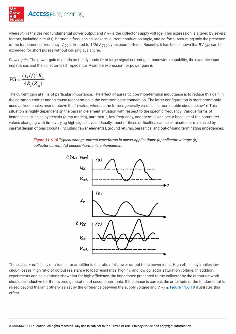
where P is the desired fundamental power output and V is the collector supply voltage. This expression is altered by severalfactors, including circuit Q, harmonic frequencies, leakage, current conduction angle, and so forth. Assuming only the presenceof the fundamental frequency, V is limited to 1/2BV by resonant effects. Recently, it has been shown that BV can beexceeded for short pulses without causing avalanche.
Power gain. The power gain depends on the dynamic f or large-signal current gain-bandwidth capability, the dynamic inputimpedance, and the collector load impedance. A simple expression for power gain is
The current gain at f is of particular importance. The effect of parasitic common-terminal inductance is to reduce this gain inthe common-emitter and to cause regeneration in the common-base connection. The latter configuration is more commonlyused at frequencies near or above the f value, whereas the former generally results in a more stable circuit below f . Thissituation is highly dependent on the parasitic-element situation with respect to the specific frequency. Various forms ofinstabilities, such as hysteresis (jump modes), parametric, low-frequency, and thermal, can occur because of the parametervalues changing with time-varying high-signal levels. Usually, most of these difficulties can be eliminated or minimized bycareful design of bias circuits (including fewer elements), ground returns, parasitics, and out-of-band terminating impedances.
Figure 11.6.18 Typical voltage-current waveforms in power applications: (a) collector voltage; (b)collector current; (c) second-harmonic enhancement.
The collector efficiency of a transistor amplifier is the ratio of rf power output to dc power input. High efficiency implies lowcircuit losses, high ratio of output resistance to load resistance, high f , and low collector saturation voltage. In addition,experiments and calculations show that for high efficiency, the impedance presented to the collector by the output networkshould be inductive for the favored generation of second harmonic. If the phase is correct, the amplitude of the fundamental israised beyond the limit otherwise set by the difference between the supply voltage and V . Figure 11.6.18 illustrates thiseffect.
o CC
CC CBO CBO
T
T
T T
T
C ,sat
© McGraw-Hill Education. All rights reserved. Any use is subject to the Terms of Use, Privacy Notice and copyright information.
A high value of f relative to the operating frequency improves efficiency by causing the operating point to spend less time (percycle) in the high-dissipation active region between cutoff and saturation. The integrity of the transistor die bond has beenfound to have a substantial effect on efficiency because of the effects of low intrinsic bulk collector resistance and thermalgradient.
11.6.9. GaAs FIELD-EFFECT TRANSISTOR CIRCUITS
The state of the art of GaAs field-effect transistors for both small-signal and power applications is rapidly improving, thanks tothe intrinsically higher carrier mobility in GaAs, coupled with significantly improved fabrication techniques, e.g., in the area ofphotolithography. Many devices fabricated today use feature sizes as small as 0.25 µm. GaAs FETs are particularly attractivesince the parameter values are less variable as a function of operating conditions and their impedances are generally higherthan in comparable bipolar devices. As a result, GaAs FET circuits are easier to design and typically achieve lower noise, widerbandwidth, and higher linearity. The common-source configuration has been found to work well for both amplifiers andoscillators.
11.6.10. NOISE PERFORMANCE OF MICROWAVE FETCIRCUITS
The noise figure of an FET can be represented as a minimum noise figure plus a noise factor which depends on the signalsource impedance presented to the FET. For an optimum signal source impedance of R + jX = R + jX , the noise figureis minimized.
K and K are fitting factors, with K depending on the channel carrier concentrations and dimensions, and K depending onthe quality of the channel material. The optimum source impedance is
It is evident that a low-noise figure requires a high cutoff frequency f , and the cutoff frequency is inversely proportional to thegate length. Therefore, a short gate length is important to low-noise operation. The noise figure can also be improved byminimizing the parasitic resistances R and R .
GaAs FETs are commercially available with noise figures less than 0.5 dB at 4 GHz, less than 1 dB at 8 GHz, and less than 2 dBat 16 GHz.
11.6.11. HIGH ELECTRON MOBILITY TRANSISTORS
T
SS SS OP OP
2 f 2 f
T
G S
© McGraw-Hill Education. All rights reserved. Any use is subject to the Terms of Use, Privacy Notice and copyright information.

11.6.11. HIGH ELECTRON MOBILITY TRANSISTORS
The performance of low-noise GaAs FETs is approaching a lower limit because of the finest gate geometry currently attainable(0.25 µm). The new high electron mobility transistor (HEMT) on GaAs offers superior performance because of its carriertransport mechanism, which resembles transport within undoped GaAs, which has little impurity scattering. The structure of anHEMT is similar to a GaAs MESFET, using a heterojunction between GaAs and AlGaAs. The carrier velocity and mobility aretwice that of carriers in a MESFET, which results in a higher cutoff frequency and lower noise figure for the same gategeometry. The following results have been achieved with HEMTs: 2 dB noise figure up to 20 GHz without cooling, and 5 dB gainwith 7.8 dB noise figure at 71 GHz.
11.6.12. HIGH-POWER MICROWAVE FET AMPLIFIERS
High-power field-effect transistors, like bipolar transistors, exhibit nonlinear device parameter variation with bias conditions.Figure 11.6.17b shows a greatly simplified equivalent circuit of a power FET. The parameters C , R , g , R , and C are biasvoltage dependent. The dominant nonlinear effects on power FET operation are the variation of the channel capacitance C with gate and drain bias voltages, the variation of the transconductance g with gate voltage, and the variation in drainresistance R with drain voltage.
The high-power performance of an FET depends mainly on the gate width, the common lead inductance and other parasitics,the transistor thermal impedance, and the maximum drain voltage capability of the device. The total gate width can beincreased by combining a number of individual cells in parallel on one chip. Cells are connected by wire bonding, “flip-chip”mounting techniques, or via-hole connections. A single FET cell may consist of many gate fingers connected in parallel bycrossover structures, or wrap-around-plating. Using these techniques total gate widths of 30 mm or more have been attained.
The bias point of the FET has an important effect on the output power capability of the amplifier circuit. The optimum loadresistance is determined from the device I-V characteristic. V is the gate-drain avalanche breakdown voltage when the FETgate is biased at pinch-off (V ). The limiting drain-source voltage is V = V − V . Beyond this voltage, excess current willflow which is unaffected by the input signal at the gate. Therefore, V is the level of V which corresponds to the maximum rfoutput power. If V is the “knee” drain voltage above which the drain current is approximately flat (independent of drain voltage),then the maximum drain voltage swing can be expressed as V − V or V − V − V . If I is the maximum drain currentavailable with a forward-biased gate, then the optimum load resistance for maximum output power is (V − V − V )/I andthe maximum rf power available to the load is I ( V − V − V )/8.
With a single high-power FET the following cw output power levels can be achieved at 1 dB gain compression: 12 W at 2 GHz, 8W at 12 GHz, and 1 W at 24 GHz. Efficiencies are typically 25 to 35 percent for class A cw operation. GaAs FETs are commonlyused in moderate power applications at microwave frequencies up to 26 GHz. Devices are frequently combined in balancedamplifier circuits to achieve higher output powers. Internally matched chip carrier structures are often used to reduce theeffects of package parasitics, and to provide low-loss matching close to the chip. One type of input circuit for an internallymatched FET comprises a small SiO chip capacitor connected to the FET gate with a bond wire, forming a π-matching sectionwith the FET input capacitance. Input and output circuits and typically LC ladder networks implemented in both discrete andsemidistributed circuit forms.
11.6.13. MONOLITHIC MICROWAVE INTEGRATED CIRCUITS
GS I m D D
GS
m
D
GD
P T GD P
L DS
K
L K GD P K F
GD P K F
F GD P K
2
© McGraw-Hill Education. All rights reserved. Any use is subject to the Terms of Use, Privacy Notice and copyright information.

11.6.13. MONOLITHIC MICROWAVE INTEGRATED CIRCUITS
Monolithic circuits, or MMICs, consist of active devices and associated circuitry fabricated together on the same substrate.GaAs MMICs are used to achieve very broad bandwidths and high-frequency operation. Because of the high area of GaAsrequired and low production yields, MMICs are very expensive. They are best suited to low- and medium-power applicationsabove 20 GHz, where high production volume is expected. The advantages of monolithic circuitry are multioctave bandwidths,millimeter-frequency operation, small size and weight. With MMICs on GaAs the following results have been attained: 4 dB gain,9 dB noise figure, and +12 dBm output power from 2 to 40 GHz with a distributed amplifier.
11.6.14. TRANSISTOR OSCILLATORS
Transistor oscillators can be designed by choosing the source (or load) terminating impedances such that Γ ≥
. The design is facilitated by plotting stability circles on the Smith chart.
A number of circuit configurations are appropriate, including the standard Colpitts, Hartley, Clapp, coupled-hybrid, and so forth.The major difference, however, is the proper inclusion of device parasitic reactances into the intended configuration. Thefrequency-determining element(s) may be in the input, output, or feedback circuit but should have a high Q for good frequencystability. Care must be taken to decouple or resistively load the circuit at frequencies outside the band where oscillatoryconditions are satisfied. This is particularly true for lower frequencies where the current gain is much better.
For bipolar transistors, the common-base and common-collector connections are generally more unstable than common-emitter and most commonly used, depending on the power requirements and frequency of oscillation.
For a GaAs FET oscillator, the device may be in common-source, gate, or drain configuration. The common grounded sourcearrangement provides the lowest thermal resistance which makes this configuration the most likely choice for a power FEToscillator. In the grounded source case a parallel feedback element is used to couple the gate and drain terminals and must besmall enough to minimize parasitics.
Figure 11.6.19 Varactor-tuned microstrip oscillator-buffer circuit.
S
© McGraw-Hill Education. All rights reserved. Any use is subject to the Terms of Use, Privacy Notice and copyright information.

Transistor oscillators have the advantage of the third terminal which may be used for compensation, modulation, orstabilization. A high-Q cavity resonator is often used in the feedback path for stabilization. The resonator may also be placedbetween the transistor and the load where it acts as a bandpass filter, or the resonator may be used as a band-reject filtercoupled to one oscillator port with the load coupled to the other oscillator port. A high dielectric constant ceramic is usuallyused for the cavity material to result in a resonator of very small physical size. Barium nanotitanate, which provides a relativedielectric constant of 39, and a Q of up to 8000, is often used as a resonator. Oscillators that use this type of stabilization arecalled dielectric resonator oscillators, or DROs.
The frequency of an oscillator which is stabilized by a dielectric resonator can be mechanically tuned by varying the gapbetween the resonator and a metal tuning plate.
Several methods are available to vary the frequency of an oscillator dynamically. Bias variation is effective only over a narrowband and results in substantial power variation. The YIG sphere provides very high Q but is somewhat bulky and of limitedtuning speed. The varactor diode provides very low power, octave-tuning bandwidth, and fast tuning in a form compatible withhybrid integration. Figure 11.6.19 shows the schematic of an S-band varactor-tuned wide-band oscillator implemented in hybridthin-film form. The frequency-determining elements are connected in the high-Q common-base input circuit. This also allowsmaximum isolation from load mismatch effects (pushing) and permits the balance of the circuitry to be low-Q (broadband).
Both high- and low-power oscillators are large-signal; i.e., the output power is limited primarily by beta falloff, with increasingcurrent at a given frequency and collector voltage.
Bipolar transistors are generally used for oscillators up to X band. Output powers of +16 dBm at 8 GHz and +7 dBm at 13 GHzhave been achieved with bipolar transistor oscillators by using a finline mount. The near carrier noise for the silicon bipolartransistor was 10 to 20 dB better than the noise characteristic of an FET oscillator operating at the same frequency.
The maximum frequency of oscillation of a GaAs FET is about 80 GHz for a 0.25 µm gate length. The following results havebeen attained at 35 GHz: +1 dBm output power and noise-to-carrier ratios of –78 dBc/Hz at 10 kHz and –87 dBc/Hz at 25 kHz.
11.6.15. TRAVELING-WAVE-TUBE CIRCUITS
The traveling-wave tube is a unique structure capable of providing high amplification of rf signals varying in frequency overseveral octaves without the need for any tuning or voltage adjustment (Sec. 7). Figure 11.6.20 shows the principal componentsof an amplifier using this tube. Electrons emitted by the electron-gun assembly are sharply focused, drawn through the length ofthe slow-wave rf structure, and eventually dissipated in the collector. Synchronism between the rf electromagnetic wave and thebeam electrons results in a cumulative interaction which transfers energy from the dc beam to the rf wave. For details on thistype of amplifier see Sec. 7.
Figure 11.6.20 Traveling-wave amplifier circuit.
© McGraw-Hill Education. All rights reserved. Any use is subject to the Terms of Use, Privacy Notice and copyright information.

Figure 11.6.21 shows the gain characteristics of a typical broadband TWT amplifier. As more energy is extracted from theelectron beam, it slows down. This loss of synchronism results in lower gains at higher power levels. One advantage of thisoverdrive characteristic is the protection of following stages against strong signals.
Traveling-wave tube amplifiers provide high gain for signals up to about 30 GHz. Power TWT technology is still advancing.TWTs are available with as high as 30 W cw output power at 12 GHz and 42 percent efficiency. Long-term reliability and noisefigure remain poor in comparison to most solid-state devices.
The backward-wave oscillator is essentially a TWT device making use of the interaction of the electron stream with anelectromagnetic wave whose phase and group velocities are 180° apart. At a sufficient beam current, oscillations are producedas discussed above, without a reverse-wave attenuator. These devices are voltage-tunable. Frequency is proportional to the halfpower of the cathode-helix voltage and the dimensions of the structure. Multioctave tuning is possible, depending on output-power-variation requirements. These oscillators have low pulling figures and, typically, high pushing figures. Frequency stabilityis excellent, usually dependent on power-supply variations. These devices are typically low power (<1 W).
Figure 11.6.21 Typical gain characteristic of a broadband TWT amplifier.
11.6.16. KLYSTRON OSCILLATORS AND AMPLIFIERS
The chief advantages of the klystron amplifier oscillator are that it is capable of large stable output power (10 MW) with goodefficiency (40 percent) and high gain (70 dB). Basically, the mechanism involves modulation of the velocity of electrons in abeam by an input rf signal. This is converted into a density-modulated (bunching) beam from which a resonant cavity extractsthe rf energy and transforms it to a useful load.
Klystron amplifiers can be conveniently divided into three categories: (1) two-resonator single-stage high-and low-noise voltageamplifiers, (2) two-resonator single stage (optimum bunching) power amplifiers, and (3) multiresonator cascade-stage voltageand power amplifiers. The power gain of a two-cavity voltage amplifier can be given by
where M , M = beam coupling factors
a = beam radius
1 2
© McGraw-Hill Education. All rights reserved. Any use is subject to the Terms of Use, Privacy Notice and copyright information.
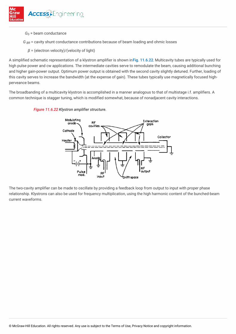
G = beam conductance
G = cavity shunt conductance contributions because of beam loading and ohmic losses
β = (electron velocity)/(velocity of light)
A simplified schematic representation of a klystron amplifier is shown in Fig. 11.6.22. Multicavity tubes are typically used forhigh pulse power and cw applications. The intermediate cavities serve to remodulate the beam, causing additional bunchingand higher gain-power output. Optimum power output is obtained with the second cavity slightly detuned. Further, loading ofthis cavity serves to increase the bandwidth (at the expense of gain). These tubes typically use magnetically focused high-perveance beams.
The broadbanding of a multicavity klystron is accomplished in a manner analogous to that of multistage i.f. amplifiers. Acommon technique is stagger tuning, which is modified somewhat, because of nonadjacent cavity interactions.
Figure 11.6.22 Klystron amplifier structure.
The two-cavity amplifier can be made to oscillate by providing a feedback loop from output to input with proper phaserelationship. Klystrons can also be used for frequency multiplication, using the high harmonic content of the bunched-beamcurrent waveforms.
11.6.16.1. Reflex Klystron
0
BR
© McGraw-Hill Education. All rights reserved. Any use is subject to the Terms of Use, Privacy Notice and copyright information.

11.6.16.1. Reflex Klystron
A simple klystron oscillator results if the electron-beam direction is reversed by a negative electrode, termed the reflector. Aschematic diagram of such a structure is given in Fig. 11.6.23. Performance data for a reflex klystron are usually given in theform of a reflector-characteristic chart. This chart displays power output and frequency deviation as a function of reflectorvoltage. Two distinct classes of reflex klystrons are low-power tubes for oscillator, pump, and test applications and higher-power tubes (10 W) for frequency-modulator applications. Operating voltage varies from 300 to 2000 V with bandwidths up to~200 MHz.
Figure 11.6.23 Reflex klystron with coaxial-line loop output.
11.6.17. CROSSED-FIELD-TUBE CIRCUITS
Practically all crossed-field tubes have integrally attached distributed constant circuits. Operation within a critical range ofbeam current is necessary to maintain the proper bandpass characteristics.
11.6.17.1. Magnetron
© McGraw-Hill Education. All rights reserved. Any use is subject to the Terms of Use, Privacy Notice and copyright information.

11.6.17.1. Magnetron
The original microwave tube was a magnetron diode switch with oscillations owing to the cyclotron resonance frequency.Several oscillator circuits were used until the standard cavity-resonator magnetron was introduced in 1940.
The relations between power, frequency, and voltage versus the load admittance are shown in the Rieke diagram (Fig. 11.6.24).Such charts illustrate the compromises necessary to obtain desired operating conditions. In general, good efficiency resultsfrom increasing anode current and magnetic field strength.
Various load effects can be considered with the Rieke diagram. The pulling figure [measure of frequency change for a definedload mismatch – (SWR) = 1.5 at all phase angles] and long-line effect are examples.
The area of highest power on the Rieke diagram is called the sink and represents the tightest load coupling to the tube. Thehighest efficiency results in this region; however, a poor spectrum or instability typically results. The buildup of oscillations inthe antisink region is closer to ideal; however, this lightly loaded condition may also result in instability. Stability is a measure ofthe percentage of missing pulses, usually defined at 30 percent energy loss.
11.6.17.2. Tuning
Methods used to tune a magnetron are classified as mechanical, electronic, and voltage tuning. In the mechanical methods, thefrequency of oscillation is changed by the motion of an element in the resonant circuit. Two types are shown in Fig. 11.6.25. Anelectron beam injected into the cavities will change the effective dielectric constant and hence the frequency. By using thefrequency pushing effect it has been possible to tune the magnetron over a frequency range of 4 to 1 (typically, 0.1 to 2 MHz/V)using voltage tuning. The frequency change is usually linear, but the power output is not constant over the tuning range.Magnetrons with power output greater than 5 MW and efficiencies 50 percent or more are available.
Figure 11.6.24 Rieke diagram for an L-band magnetron at 1250 MHz. Solid curves are contours ofconstant power; dashed curves of constant frequency. (Raytheon Company.)
11.6.17.3. Amplitron
© McGraw-Hill Education. All rights reserved. Any use is subject to the Terms of Use, Privacy Notice and copyright information.

11.6.17.3. Amplitron
The Amplitron is essentially a magnetron with two external couplings, enabling amplifier operation. It is characterized by highpower, broad bandwidth, very high efficiency, and low gain. The output is independent of rf input but dependent on dc input. Itacts as a low-loss passive transmission line in the absence of high voltage. A typical plot of power for an Amplitron is shown inFig. 11.6.26. Conversion efficiency of an Amplitron can be as high as 85 percent. The gain can be increased by insertingmismatches into the input and output transmission lines.
11.6.18. GYROTRON CIRCUITS
Beyond 30 GHz, the power available from classical microwave tubes declines sharply. The gyrotron offers the possibility of highpower at millimeter wave frequencies.
The gyrotron is a cyclotron resonance maser. The structure of the gyrotron includes a cathode, a collector, and a circularwaveguide of a gradually varying diameter. Electrons are emitted at the cathode with small variations in speed. The electroncurrent density is very high. The electrons are accelerated by an electric field and guided by a static magnetic field. Thenonuniform induction field causes the rotational speed of the electrons to increase, which in turn causes the linear velocity ofthe electrons to decrease, while they follow a helical trajectory. The microwave field exists within the circular waveguide, wherethe cutoff of the mode is only slightly above the microwave signal frequency. The electrons give up energy because ofinteraction with the field of the rotating mode. This causes bunching of the electrons, similar to the bunching within a klystron.Finally there is a decompression zone where the induction decreases and the electrons are collected.
Figure 11.6.25 Mechanical magnetron tuning mechanisms: (a) capacitance type; (b) inductancetype.
© McGraw-Hill Education. All rights reserved. Any use is subject to the Terms of Use, Privacy Notice and copyright information.

Figure 11.6.26 Gain characteristic of model QK520 L-band amplifier.
The smooth shape of the gyrotron circular waveguide produces less loss than other microwave tubes. The power available witha gyrotron is 100 or more times greater than that available from classical microwave tubes at the same frequency. The outputpower levels which can be attained with a gyrotron in cw operation are as follows: 12 kW at 107 GHz and 31 percent efficiency,or 1.5 kW at 330 GHz and 6 percent efficiency.
Trademark of the Hewlett Packard Co.
Trademark of the Hewlett Packard Co.
Here, the plot of YT (ω) represents the case of Z (ω) short-circuited; however, similar plots can be obtained for more general cases.
It is assumed that the statistical weights are equal to 1.
[*]
[*]
[*] T e
[*]
© McGraw-Hill Education. All rights reserved. Any use is subject to the Terms of Use, Privacy Notice and copyright information.