Applications of Semiconductor Optical Amplifiers - UILIS ...
158
Applications of Semiconductor Optical Amplifiers Kyriakos E. Zoiros www.mdpi.com/journal/applsci Edited by Printed Edition of the Special Issue Published in Applied Sciences applied sciences
-
Upload
khangminh22 -
Category
Documents
-
view
1 -
download
0
Transcript of Applications of Semiconductor Optical Amplifiers - UILIS ...

Applications of Semiconductor Optical Amplifiers
Kyriakos E. Zoiros
www.mdpi.com/journal/applsci
Edited by
Printed Edition of the Special Issue Published in Applied Sciences
applied sciences

Applications of Semiconductor Optical Amplifiers

Applications of SemiconductorOptical Amplifiers
Special Issue Editor
Kyriakos E. Zoiros
MDPI • Basel • Beijing • Wuhan • Barcelona • Belgrade

Special Issue Editor
Kyriakos E. Zoiros
Democritus University of Thrace
Greece
Editorial Office
MDPI
St. Alban-Anlage 66
Basel, Switzerland
This is a reprint of articles from the Special Issue published online in the open access journal
Applied Sciences (ISSN 2076-3417) from 2017 to 2018 (available at: http://www.mdpi.com/journal/
applsci/special issues/optical amplifiers)
For citation purposes, cite each article independently as indicated on the article page online and as
indicated below:
LastName, A.A.; LastName, B.B.; LastName, C.C. Article Title. Journal Name Year, Article Number,
Page Range.
ISBN 978-3-03897-170-2 (Pbk)
ISBN 978-3-03897-171-9 (PDF)
Articles in this volume are Open Access and distributed under the Creative Commons Attribution
(CC BY) license, which allows users to download, copy and build upon published articles even for
commercial purposes, as long as the author and publisher are properly credited, which ensures
maximum dissemination and a wider impact of our publications. The book taken as a whole isc© 2018 MDPI, Basel, Switzerland, distributed under the terms and conditions of the Creative
Commons license CC BY-NC-ND (http://creativecommons.org/licenses/by-nc-nd/4.0/).

Contents
About the Special Issue Editor . . . . . . . . . . . . . . . . . . . . . . . . . . . . . . . . . . . . . . vii
Preface to ”Applications of Semiconductor Optical Amplifiers” . . . . . . . . . . . . . . . . . . ix
Christos Vagionas, Pavlos Maniotis, Stelios Pitris, Amalia Miliou and Nikos Pleros
Integrated Optical Content Addressable Memories (CAM) and Optical Random AccessMemories (RAM) for Ultra-Fast Address Look-Up OperationsReprinted from: Appl. Sci. 2017, 7, 700, doi: 10.3390/app7070700 . . . . . . . . . . . . . . . . . . . 1
Zoe V. Rizou, Kyriakos E. Zoiros and Antonios Hatziefremidis
Comparison of Basic Notch Filters for Semiconductor Optical Amplifier PatternEffect MitigationReprinted from: Appl. Sci. 2017, 7, 783, doi: 10.3390/app7080783 . . . . . . . . . . . . . . . . . . . 19
Sean P. O Duill, Pascal Landais and Liam P. Barry
Estimation of the Performance Improvement of Pre-Amplified PAM4 Systems When UsingMulti-Section Semiconductor Optical AmplifiersReprinted from: Appl. Sci. 2017, 7, 908, doi: 10.3390/app7090908 . . . . . . . . . . . . . . . . . . . 41
Simon Arega Gebrewold, Romain Bonjour, Romain Brenot, David Hillerkuss and
Juerg Leuthold
Bit- and Power-Loading—A Comparative Study on Maximizing the Capacity of RSOA BasedColorless DMT TransmittersReprinted from: Appl. Sci. 2017, 7, 999, doi: 10.3390/app7100999 . . . . . . . . . . . . . . . . . . . 54
Zoe V. Rizou and Kyriakos E. Zoiros
Theoretical Analysis of Directly Modulated Reflective Semiconductor Optical AmplifierPerformance Enhancement by Microring Resonator-Based Notch FilteringReprinted from: Appl. Sci. 2018, 8, 223, doi: 10.3390/app8020223 . . . . . . . . . . . . . . . . . . . 71
Nicola Calabretta, Wang Miao, Ketemaw Mekonnen and Kristif Prifti
SOA Based Photonic Integrated WDM Cross-Connects for Optical Metro-Access NetworksReprinted from: Appl. Sci. 2017, 7, 865, doi: 10.3390/app7090865 . . . . . . . . . . . . . . . . . . . 88
Ripalta Stabile
Towards Large-Scale Fast Reprogrammable SOA-Based Photonic Integrated Switch CircuitsReprinted from: Appl. Sci. 2017, 7, 920, doi: 10.3390/app7090920 . . . . . . . . . . . . . . . . . . . 101
Yi Lin, Aravind P. Anthur, Sean P. O Duill, Fan Liu, Yonglin Yu and Liam P. Barry
Fast Reconfigurable SOA-Based Wavelength Conversion of Advanced Modulation Format Data
Reprinted from: Appl. Sci. 2017, 7, 1033, doi: 10.3390/app7101033 . . . . . . . . . . . . . . . . . . 116
Md Shakil Ahmed and Ivan Glesk
Application of Semiconductor Optical Amplifier (SOA) in Managing Chirp of Optical Code Division Multiple Access (OCDMA) Code Carriers in Temperature Affected Fibre LinkReprinted from: Appl. Sci. 2018, 8, 715, doi: 10.3390/app8050715 . . . . . . . . . . . . . . . . . . . 131
v


About the Special Issue Editor
Kyriakos E. Zoiros (born 1973 in Thessaloniki, Greece) is an Associate Professor at the Department of Electrical and Computer Engineering, Democritus University of Thrace (DUTH), Xanthi, Greece. He holds a Ph.D. degree on optical communications from the Photonics Communications Research Laboratory, National Technical University of Athens, Greece. He is the author or coauthor of more than 100 journal and conference papers, some of which were invited, as well as of five book chapters. His published work has received a considerable number of citations (>1000, h-index = 20, source Scopus). In 2009, he was seconded to the Optical Communications Research Group, University of Limerick, Ireland, and in 2013 to the Ecole Nationale d’Ingenieurs de Brest (ENIB), France. His current research interests include applications of semiconductor optical amplifiers, applications of microring resonators, microwaves photonics, and free space optical communications.
vii


Preface to ”Applications of Semiconductor
Optical Amplifiers”
During recent years, the technology of semiconductor optical amplifiers (SOAs) has been evolving remarkably and has matured to the point where it is presently established as a key enabler for the development, implementation, optimization, and overall establishment of photonic circuits, subsystems, and networks. Owing to the outstanding advancements that have been achieved in the field, SOAs are commercially available devices that exhibit several important properties, such as strong nonlinearities, low power consumption, wavelength flexibility, a large dynamic range, fast response, broadband and versatile operation, small footprint, and the capacity for scalable integration in single chips at an affordable cost. These attractive characteristics have rendered SOAs core elements for the accomplishment of critical and indispensable tasks at the fundamental and system-oriented level. Thus, SOAs have widely been adopted both by the research community and the industrial sector as a principal technological platform for the realization of a diverse range of applications with high performance.
Given the huge practical potential of SOAs, this book contains papers published within the frame of a Special Issue on ‘Applications of Semiconductor Optical Amplifiers’, with a twofold aim. On one hand, it sought to address, present, and investigate modern applications of SOAs, and on the other hand, to explore and highlight trends, challenges, and perspectives to motivate efforts toward the continuous exploitation of these active modules in a feasible, innovative, and global manner. This book collates the Special Issue papers reporting on the significant results obtained from the cutting-edge research conducted by experts in the field. The compilation can provide useful knowledge and open new horizons regarding SOA-enabled applications, such as direct signal amplification, external modulation, all-optical signal processing, all-optical memories, photonic integrated circuits, photonic switching, optical code division multiple access systems, and passive optical networks.
The research field of integrated optical memories was covered by C. Vagionas, P. Maniotis, S. Pitris, A. Miliou, and N. Pleros. This paper describes a novel application scenario for optical memories based on monolithically integrated SOA and Mach-Zehnder interferometer layouts/arrangements. In this context, it proposes an alternative path to circumvent the mismatch between the rapidly growing optical transmission line rates and electronic processing speeds to facilitate technological evolution in the era of the Internet of Things.
The use of SOAs for optical signal amplification applications is reported in two papers.
Z.V. Rizou, K.E. Zoiros, and A. Hatziefremidis present a theoretical analysis and benchmarking of
two basic optical notch filters employed to compensate for the SOA pattern effect. The comparison
reveals the performance merits of each filter that allow it to favorably compete against the other to
efficiently address the pattern-dependent operation of SOAs and assisting the latter in serving linear
amplification applications with improved performance.
S.P. O Duill, P. Landais, and L.P. Barry propose multi-section SOAs as pre-amplifiers for short
range optical communication links within datacenters. By creating and employing a simplified
multi-section SOA model, they evaluate the performance benefits offered by these special type SOAs,
which are shown to exhibit a better input power dynamic range than conventional single-section
SOAs when amplifying single- as well as multi-channel signals in the advanced modulation format
(four-level pulse amplitude modulation/PAM4).
ix

Reflective semiconductor optical amplifiers (RSOAs) are the subject of two papers. S.A. Gebrewold, R. Bonjour, R. Brenot, D. Hillerkuss, and J. Leuthold conduct a comparative study of the capacity increase brought in wavelength division multiplexing (WDM) passive optical network (PON) architectures by exploiting bit- and power-loading discrete multi-tone (DMT) modulation in upstream colorless transmitters using RSOAs. Three different RSOA-based schemes are compared against appropriate evaluation criteria whose measurement and analysis allows them to specify and highlight performance and cost trade-offs. Concurrently, record high line rates in both back-to-back and transmission experiments were obtained and reported for all three configurations.
Z.V. Rizou and K.E. Zoiros demonstrate the feasibility of using a single microring resonator (MRR) as an optical notch filter to enable RSOA direct modulation at an extended data rate compared to what is possible with the RSOA alone. To this aim, it was investigated and specified how the MRR should be designed to improve the encoded signal characteristics for RSOA direct modulation applications.
The exploitation of SOAs for photonic switching purposes is addressed in two papers.
N. Calabretta, W. Miao, K. Mekonnen, and K. Prifti present a novel photonic WDM optical
cross-connect node based on SOAs that allows switching data signals in wavelength, space, and time
to fully exploit statistical multiplexing. Also, they report on the experimental assessment of this core
building block for interconnecting network elements as well as computing and storage resources,
which verifies the advantages of using SOAs to realize the WDM cross-connect switch in terms of
transparency, switching speed, photonic integrated amplification for lossless operation, and gain
equalization.
R. Stabile reviews the current status of fast reconfigurable medium-scale indium phosphide (InP)
integrated photonic switch matrices based on the use of SOA gates. The focus is on broadband
and cross-connecting monolithic implementations that grant multi-input/output port and channel
connectivity based on a packet-compliant SOA multi-stage switching matrix. The opportunities for
increasing connectivity, enabling nanosecond-order reconfigurability, and introducing distributed
optical power monitoring at the physical layer are highlighted. Furthermore, complementary
architectures based on resonant switching elements developed on the same material platform for
power efficient switching are considered. Lastly, performance projections related to the physical layer
are presented, and strategies for improvements in view of opening a route towards large-scale power
efficient fast reprogrammable photonic integrated switching circuits are discussed.
The leveraging of SOAs as nonlinear elements in the context of all-optical functionalities is treated
by Y. Lin, A.P. Anthur, S. P. O Duill, F. Liu, Y. Yu, and L.P. Barry. In particular, a wavelength converter
is developed, which is comprised of an SOA that takes advantage of four wave mixing (FWM) and a
fast-switching sampled grating distributed Bragg reflector (SG-DBR) tunable laser as one of the pump
sources. By studying phase noise issues in FWM as well as vector theory in SOAs in conjunction
with a detailed characterization of the SGDBR laser, rapid and reconfigurable wavelength conversion
is experimentally demonstrated on bursty/packet data of advanced modulation formats towards
dynamic, adaptive and bandwidth-efficient next generation transparent optical networks.
x

Finally, the research activity on optical code division multiple access (OCDMA) is presented by
M.S. Ahmed and I. Glesk. This paper explores the use of SOAs in the transmitter side of such
a system based on multi-wavelength picosecond code carriers for the mitigation of the temporal
distortion of an OCDMA auto-correlation affected by the temperature-induced dispersion changes
in a fiber optic transmission link. To this aim, it is shown both experimentally and using simulations,
that a distorted OCDMA auto-correlation due to the temperature-induced fiber dispersion can be
corrected by manipulating the chirp of code carriers when traversing a biased SOA prior to entering
the transmission link.
I would like to thank all those who contributed to making this book possible.
Kyriakos E. Zoiros
Special Issue Editor
xi


applied sciences
Article
Integrated Optical Content Addressable Memories(CAM) and Optical Random Access Memories (RAM)for Ultra-Fast Address Look-Up Operations
Christos Vagionas *, Pavlos Maniotis, Stelios Pitris, Amalia Miliou and Nikos Pleros
Department of Informatics, Aristotle University of Thessaloniki, 54124 Thessaloniki, Greece;[email protected] (P.M.); [email protected] (S.P.); [email protected] (A.M.); [email protected] (N.P.)* Correspondence: [email protected]; Tel.: +30-231-0990-588
Academic Editor: Kyriakos E. ZoirosReceived: 30 May 2017; Accepted: 4 July 2017; Published: 7 July 2017
Abstract: Electronic Content Addressable Memories (CAM) implement Address Look-Up (AL) tablefunctionalities of network routers; however, they typically operate in the MHz regime, turning ALinto a critical network bottleneck. In this communication, we demonstrate the first steps towardsdeveloping optical CAM alternatives to enable a re-engineering of AL memories. Firstly, we reporton the photonic integration of Semiconductor Optical Amplifier-Mach Zehnder Interferometer(SOA-MZI)-based optical Flip-Flop and Random Access Memories on a monolithic InP platform,capable of storing the binary prefix-address data-bits and the outgoing port information for nexthop routing, respectively. Subsequently the first optical Binary CAM cell (B-CAM) is experimentallydemonstrated, comprising an InP Flip-Flop and a SOA-MZI Exclusive OR (XOR) gate for fastsearch operations through an XOR-based bit comparison, yielding an error-free 10 Gb/s operation.This is later extended via physical layer simulations in an optical Ternary-CAM (T-CAM) cell anda 4-bit Matchline (ML) configuration, supporting a third state of the “logical X” value towardswildcard bits of network subnet masks. The proposed functional CAM and Random AccessMemories (RAM) sub-circuits may facilitate light-based Address Look-Up tables supporting searchoperations at 10 Gb/s and beyond, paving the way towards minimizing the disparity with the franticoptical transmission linerates, and fast re-configurability through multiple simultaneous WavelengthDivision Multiplexed (WDM) memory access requests.
Keywords: Optical Content Addressable Memories; Optical Random Access Memories; AddressLook Up; Optical Matchline; Semiconductor Optical Amplifier Mach Zehnder Interferometers;photonic integration; monolithic InP platform
1. Introduction
The last decades have been marked by the widespread use of bandwidth-hungry internetapplications by multiple wireless users and cloud-network devices always connected online. This hasled to an immense Internet expansion [1], enabled by the rapid advances in photonic integration [2]and optical transceiver technologies that achieve doubling of the optical transmission line-rates everyyear [3]. Meanwhile, Internet topologies have strongly relied on resilient multi-homing techniquesand on the Virtual Private Network (VPN) for enhanced network resiliency or security, necessitatingadditional physical or logical communication links [4]. The insatiable interconnectivity demands haveresulted in an enormous surge in the number of addressable end-points [1,4], even running up to thecomplete exhaustion of the unallocated IPv4 address pool [5], enforcing the use of the next generationIPv6 protocol. IPv6 offers a higher availability for address space, but at the same time, quadruples theneeds of Address Look-Up (AL), while scaling at a frantic annual growth rate of 90% [6]. As a result,
Appl. Sci. 2017, 7, 700; doi:10.3390/app7070700 www.mdpi.com/journal/applsci1

Appl. Sci. 2017, 7, 700
the Default Free Zone (DFZ) has been constantly expanding, with the Routing Information Base (RIB)of Internet core routers increasing up to 700 K prefix-entries [7], requiring increasingly more searchintensive operations to resolve the outgoing port of an incoming packet. Moreover, recent studies onthe content centric nature of today’s internet usage have even inspired Content Centric Networking(CCN) [8] that investigates a clean slate future internet, where packet forwarding will operate basedon content addressing, instead of addressing the destination end-host, yet this would tremendouslyscale the respective name look-up requirements. As performance sensitive AL operations have to beperformed at wire speed upon the arrival of the packet [4], this has rendered software algorithmicsearch approaches with sequential access schemes to Random Access Memories (RAMs) as ratherimpractical since the early 2000s [4], necessitating specialized electronic hardware AL-solutions [9,10].
Presently, routers rely on electronic Content Addressable Memories (CAMs) that facilitate ALtable functionalities within one clock cycle [10]. CAMs offer content-based addressing of the storeddata, instead of location-based addressing, forming an alternative to conventional RAMs of computingarchitectures [11,12]. Specifically, upon the arrival of a packet, its destination address is inserted intoa CAM-table for a fast parallel comparison across the AL memory contents, and upon a match, theoutgoing port is obtained for next hop routing. In order to comply with the Classless InterdomainRouting (CIDR) [13], CAMs have also been equipped with ternary features, to support wildcardbits of network subnets, that mask the stored RIB-prefixes at arbitrary bit-positions with a “logicalX” value [10]. Early fast demonstrations of such Ternary CAM (T-CAM) devices built on 250 nmComplementary Metal–Oxide–Semiconductor (CMOS) nodes supported content comparisons at260 MHz [14], while similar T-CAMs at 180 nm [15], 130 nm [16], or 62 nm [17] CMOS nodes achievedmaximum frequencies of 210 MHz, 200 MHz, and 400 MHz, respectively. Despite the rich varietyof optimization techniques of mature electronic technology, state of the art electronic CAMs arescaling at a slow growth rate [18,19], and even by shifting to advanced 28 nm CMOS Fully DepletedSilicon-On-Insulator (FD-SOI) [20], only footprint and power reductions have been achieved, withfrequencies still lying around 370 MHz. These results imply that electronic T-CAMs are hard-limitedby the underlying interconnect network and can rarely reach the barrier of 1 Gb/s. This barrier wasonly recently broken using alternative non-optimal techniques that may use early predict/late-correctschemes [21], which are yet known to be heavily dependent on data patterns [17]. A second speedenhancement technique suggests inserting four T-CAM arrays performing in parallel at a slower rateof 4 × 400 MHz [6], necessitating even more complex Application Specific Integrated Circuit (ASIC)for deserialization and further exacerbating the energy requirements of routers, which reached theirrack-power density limits in 2005 [4,22,23]. To this end, electronic CAM speeds seem inefficient to keepup with the frantic optical linerates of 100 Gb/s and beyond [1]. This performance disparity has beenplacing an increasingly heavy load on the shoulders of electronic CAMs, enforcing energy-hungry,cost-expensive optoelectronic header conversions with subsequent data-rate down-conversion [22–24],in order to perform AL searches in the MHz-regime. Furthermore, the migration towards SoftwareDefined Networks (SDN) and OpenFlow networks enforces a dynamic operation with frequentupdates of network topologies and multiple real time changes in the RIB-list [25]. Internet routers areexperiencing 100 updates per second and potentially reaching upwards of 1000 per second [26], duringwhich AL operations are stalled and the router remains idle, considerably limiting the performance.This, in-turn, requires fast Write operations to the CAM-table, with short latencies [25–28], to enablefast re-configurability of the network and rapid updating of the AL table.
Having detected the impact of slow-performing AL operations, optics have tried to circumventthe associated delays, mainly through the use of optical labeling and header processing schemes.These insert a bit-serial label in front of the payload or various multiplexing schemes, to route the databased on this label instead of the actual destination IP address [29], yet they typically utilize lowerlabel data-rates, hoping to retain compatibility with slow CAM speeds. At the same time, opticalmemories have undergone two decades of developments and are now on the verge of developinghigher capacity [30], programmable [31], and/or non-volatile [32] devices towards more practical
2

Appl. Sci. 2017, 7, 700
memory sub-systems. Initially, optical memories were conceived as high bandwidth alternatives ofelectronic RAMs to overcome the “Memory Wall”, achieving multiple elementary Flip-Flops (FFs) withhigh speed and low power consumption credentials [33–41], including coupled SOAs [34], III-V-on-SOImicrodisk lasers [35], and polarization bistable Vertical Cavity Surface Emitting Laser (VCSEL) [36], aswell as coupled SOA-based Mach-Zehnder Interferometers (SOA-MZIs) [33,37]. Optical FFs, servingas optical storing units, were then combined with random access controlling gates, forming functionaloptical RAMs, so far demonstrated either as fully functional architectures using mature SOA-baseddevices [37–39] or as discrete components based on photonic crystals [40,41]. These have both beenexperimentally shown to support speeds beyond 10 Gb/s, while in-depth frequency theoreticalmemory speed analyses [42,43] and validated time-domain SOA-based memory simulations [43,44]have revealed potential rates of up to 40 Gb/s. Furthermore, by combining optical Column/RowAddress Selectors [45,46] and optical Tag Comparators [47], the first designs of a complete optical cachememory architecture for high-performance computers revealed a 16 GHz operation via physical layersimulations [48]. All of these have increased the maturity of optical memories towards penetrating thecomputing domain, where the use of electronics is so far undisputable, whereas in optical networks,optical FFs have been suggested for contention resolution [49].
Following the paradigm of optical RAMs, optical alternatives of CAM architectures may facilitatesimilar advances and speed enhancements towards ultra-fast router AL memories in the high-endrouter domain. In this regime, some preliminary first steps, stemming from our group, have managedto develop the first photonic alternative CAM-based elements [50,51], which is the main focus ofthis paper. More specifically, in Section 2, we initially discuss the architectures and main functionalbuilding blocks of electronic AL memories, followed by the development of monolithic photonicintegration for optical FFs and RAM memories on a monolithic InP platform [33,39] in Section 3.In Section 4, we present the first experimental proof-of-principle of an all-optical Binary CAM (B-CAM)cell architecture at 10 Gb/s [50]. This architecture is later extended in a more advanced all-optical(T-CAM configuration in Section 4, directly supporting, for the first time, a wildcard bit operationof a logical “X” value in the optical domain [51]. By introducing Wavelength encoding in the searchword, a 4-bit Matchline (ML) architecture is developed, capable of providing a unique identifyingsignal upon a match of the destination address with the stored prefix-entry [51]. Finally, we present adiscussion on the future challenges that need to be addressed for migrating towards optical AL tablearchitectures, bearing promises to directly resolve the AL in the optical domain that can significantlyspeed-up AL-speeds in high-end router architectures.
2. Electronic Address Look-Up Memory Architectures
Internet routers forward the data packets of an incoming port to an outgoing port based on an ALcomparison function of the destination address of the header. To achieve this, they are equipped witha hardware look-up table that maintains the RIB-list of the destination addresses and their associatedoutgoing ports for next-hop routing, as depicted in the AL memory table architecture of Figure 1a.The architecture comprises a two dimensional CAM table inter-connected to a two dimensional RAMtable. The CAM table stores the prefix-list with the destination addresses, while the RAM tablemaintains the outgoing port. Each entry of the RIB prefix-list is stored in a mutli-bit memory line,widely known as CAM ML. Upon the arrival of a packet, the header containing the destination addressbits is broadcasted to all MLs of the CAM table, where it gets bitwise compared with the contentsof the CAM cells. When the stored word of a specific ML matches the incoming search bits of thedestination address, a match-signal is generated at the output of the ML, activating the specific line;otherwise, the CAM ML is not enabled. The activated CAM ML can then be mapped though theintermediate encoder-decoder network to the associated RAM table line, where the next-hop routinginformation is stored, so as to retrieve the outgoing port of the data packet. An example operation ofthe AL table is described by the RIB table shown at the right side of Figure 1a, assuming an incomingpacket designated with a destination address [0111] and an RIB-list with four entries, namely [001X],
3

Appl. Sci. 2017, 7, 700
[010X], [011X], and [10XX]. By broadcasting and bit-wise comparing the destination address with allthe RIB-entries, the third prefix of [011X] matches the packet’s destination address. This matching willin turn activate the third line of the RAM forwarding table where port C is stored, indicating the nexthop to which the incoming packet has to be forwarded.
Figure 1. (a) Electronic AL memory architecture comprising a T-CAM table interconnected to a RAMtable and the respective router Routing Information Base (RIB) list; (b) Logical circuit of an electronicMatchline architecture; and (c) the standard electronic 16T Not OR (NOR) T-CAM cell architecture.
A more detailed view of the block diagram describing the logical circuit operation of the 1 × 4 MLis shown in Figure 1b, comprising four parallel CAM cells. The CAM cells have their outputs combinedat an inline Sense Amplifier (SA) and are then inter-connected to the encoder/decoder network forcommunication with the RAM table. Every CAM cell stores a bit of a RIB prefix entry and bears alogical XNOR gate for comparison with the incoming search bits of the destination address. If thesearch bit and the stored bit are equal, the logic XNOR gate transmits a signal of logic “1” value to theend of the respective ML. Equivalently, when all CAM cells of the line provide a logical match, the SAidentifies the exact word match with the stored content and emits a proper signal towards the encoder.On the contrary, when there is a mismatch at any of the bits of the ML, the XNOR gate of the CAMcell provides a logical “0” value at the output, and de-activates the SA and the ML, denoting that amismatch between the incoming destination address and the stored prefix has occurred. At this point,it is worth noting that MLs consist of Ternary T-CAM cells, in order to support ternary features withmasked wildcard bits of “logical X”, as used in subnet masks, rather than simpler Binary CAM cellsthat store only bits of logical “1” or “0”.
The conventional architecture of the most typical 16T NOR-based electronic T-CAM cell isillustrated in Figure 1c [10], comprising two D-type flip-flops operating as storage cells and markedwith a blue highlight. The first memory cell is responsible for storing the actual data-bit [0 or 1] and thesecond one stores the ternary state information for the “Care” or “Don’t Care” state of the logical “X”value. Each memory cell is typically built on the configuration of two cross-coupled inverters, similarto 6T RAM cells [11], while another two pairs of transistors, (M1, M3) and (M2, M4), form short–circuitsto the ground. This configuration ensures that at least one pulldown path from the ML down to theground exists at any time during a mismatch between the search word and the stored data. On thecontrary, a match between the search word bit and the stored data disables both pulldown paths,disconnecting the ML from the ground and feeding its output to the SA. If this matching happensfor all the cells of the ML, a NOR logic operation between all CAM outputs, performed at the SA,identifies the exact match of the packet’s destination address with the certain RIB prefix entry.
4

Appl. Sci. 2017, 7, 700
3. Monolithic Photonic Integration for Optical Memories
To this end, photonic integration processes have matured to the point where a wealth of opticalFF and RAM memory configurations have been successfully demonstrated [33–41], with most of thesedemonstrations relying on the mature SOA switching technology, owing to its high-gain, high-speed,and high-yield performance characteristics [2]. In this paper, our analysis draws from the architectureof an FF memory with two cross-coupled asymmetric SOA-MZI switches, as illustrated in Figure 2a,which was initially developed in [37] and more recently theoretically investigated in the time andfrequency domain in [43]. Each SOA-MZI switch features one SOA (SOA1 and SOA2) at the lowerbranch and a phase shifting element (Φ1 and Φ2) at the upper branch for controlling the biasingconditions of the interferometer. The two SOA-MZIs (SOA-MZI1 and SOA-MZI2) are each poweredby a weak Continuous Wavelength (CW) input signal at wavelengths λ1 and λ2, respectively, whiletheir Unswitched output ports (U-ports) are interconnected through a common coupling waveguidepath. This symmetric configuration of the two SOA-MZI switches allows for a master-slave operationwith the U-output of the master switch controlling the operating condition of the opposite slave switchand blocking its transmission at the U-port. Owing to the symmetric configuration, the roles of themaster and slave switch are interchangeable, allowing the FF state to be defined by the wavelength ofthe emitted signal outputs at either one of the Switched ports (S-ports). The FF state can be monitoredthrough the respective FFOut1 and FFOut2 output ports in terms of high power levels of λ1 and λ2optical signals, respectively.
Figure 2. (a) All-optical Flip-Flop architecture and operation; (b) Mask-layout of the fabricatedmonolithic InP Flip-Flop; (c) Image of the packaged Flip-Flop device with electrical/optical connectionsand TEC element; and (d) Microscope image of the fabricated Flip-Flop device.
The state of the FF can be optically controlled by external Set/Reset (SR) pulses fed through theS-ports of the SOA-MZIs. When a high Set or Reset pulse is injected at the master SOA-MZI, it willblock its light-transmission and set it in the slave condition regardless of the previous state of the FF,allowing for the opposite SOA-MZI to recover and become the master. In this arrangement, the twological values of the data-bit stored in the FF-memory, logical “1” and “0”, can be associated with thehigh optical power of the wavelength-signal emerging at the two outputs. The present FF memoryconfiguration was initially demonstrated as a hybridly integrated module in [37] with the use ofsilica-on-silicon integration technology, exhibiting a total footprint of 45 × 12 mm2 and coupling lengthbetween the two SOAs of 2.5 cm, which was theoretically shown to be the main speed determiningfactor of the memory architecture [42,43].
Following the conclusions drawn by the underlying theory on the critical performanceparameters [42,43], an integrated version of the SR FF was presented using library-based components ofa generic monolithic InP platform [33], to benefit from an integration technique that offers the possibilityto fabricate multiple active and passive photonic components on a single chip at a close proximity. Thetwo SOA-MZI switches were fitted in a die footprint-area of 6 × 2 mm2 and cross-coupled together
5

Appl. Sci. 2017, 7, 700
through a 5 mm-long coupling waveguide. In this configuration, the intra FF coupling waveguidewas 5 mm-long, reducing the total footprint by two orders of magnitude, compared to the previoushybridly-integrated FF implementation [37]. The mask file of the Photonic Integrated Chip (PIC) isillustrated in Figure 2b. The input MMI couplers of the asymmetric MZIs featured a cross/throughcoupling ratio of 70/30, with respect to the SOA elements, and the MMIs between the two SOA-MZIsfeatured a coupling ratio of 50/50. The two SOAs featured an active length of 1 mm, while the biasingof the SOA-MZIs was achieved through the respective current injection phase shifters. Electricalrouting of the metal wires connected the anodes and cathodes of the SOAs and the phase shifters to100 × 100 μm2 pads at the upper edge of the chip. The chip featured an array of eight zero-angledSpot Size Converters (SSC) with a pitch of 127 μm for optical I/O connectivity.
The monolithic InP FF-chip was fabricated by Fraunhofer Heinrich-Hertz-Institut (HHI) within aMulti-Project Wafer (MPW) run of the PARADIGM project funded by the European Commission andwas later fully packaged in terms of the optical and electrical contacts for system level characterization.The chip was mounted on top of a ceramic sub-mount module, equipped with a thermistor and aPeltier element for temperature stability, while an 8-I/O fiber array was permanently glued to theI/O left facet of the chip. The metal pads of the chip were wire-bonded to the gold-plated ceramicmount, through gold wires, which also facilitated further connectivity with a Printed Circuit Board(PCB), where a 26-pin D-connector was mounted. The fully-packaged chip can be seen in Figure 2cand a microscope image of the PIC is shown in Figure 2d. The FF device was fully characterized interms of its active components, i.e., the SOAs and the phase shifters, and was used to experimentallydemonstrate a successful Set-Reset FF operation at 10 Gb/s [33], highlighting the potential to store andwrite data directly in the optical domain.
The present monolithic FF architecture served as the memory element of a more complex opticalRAM cell configuration, capable delivering Read/Write and Block Access operations. To achieve this,the optical FF is combined with an SOA-MZI optical Access Gate (AG) in a cascade configuration,as shown in Figure 3a. The AG is responsible for granting access to the RAM cell by allowing thedata to be either written to or read from the FF each time. The input Data signals are connected to theinput of the SOA-MZI AG, and subsequently to an Arrayed Waveguide Grating (AWG) demultiplexerthat drives each wavelength to the input/output ports of the FF-memory. The control signal is fed tothe upper branch of the SOA-MZI AG, to induce Cross-Phase Modulation (XPM) phenomena. Thisallows the bit and bit signals to pass through the AG switch and emerge at the U-port, when there isno control pulse present, or at the S-port when a control pulse is present. RAM cell operations are thendefined based on the values of the logic pulses of the Inverted Access signal and the bit and bit signals,which are fed to the RAM I/O Data port and Access port.
Figure 3. (a) Optical RAM cell architecture; and (b) Experimental layout used for an evaluation of theRAM Read/Write operation.
6

Appl. Sci. 2017, 7, 700
During the Write operation, when access is granted to the memory, the complementary bit and bitsignals carry the incoming data word wavelength encoded on two different wavelengths, while theInverted Access signal features a logical “0” pulse. Then, the external bit and bit signals pass through theAG U-port, and propagate towards the right side, where they are demultiplexed through the AWG andfed to the two inputs of the FF, acting as Set and Reset signals. During the Read operation, the InvertedAccess signal again features a logical “0” pulse, while no external data are transmitted to the RAM cell.In this case, the complementary FF output signals, propagating from the FF towards the AG on the leftside, are multiplexed in the AWG and fed to the AG through the U-port, so as to emerge at the outputof the RAM cell. When access to the memory is blocked, the Inverted Access signal features a logical “1”pulse, which enters the SOA-MZI AG as the control signal, switching the complementary data signalsto the S-port and blocking communication with the outer world, allowing for the FF-memory to retainits logic state and memory content.
The experimental setup used to evaluate the complete RAM functionalities is illustrated inFigure 3b. A signal generator (SG) was used to drive a Programmable Pattern generator (PPG) at5 GHz. The PPG drives two Ti: LiNbO3 modulators using complementary bit-patterns in order toproduce 5 Gb/s 27 − 1 Pseudorandom Binary Sequences (PRBS) Non-Return-to-Zero (NRZ) signals.One modulator is responsible for producing the Inverted Access signal at 1554.8 nm and the bit signalat 1558.7 nm, and the other is used for the bit signal at 1557.9 nm. For the evaluation of the Writeoperation, the three signals were coupled together to form the complementary bit and bit pair andone access signal, while the two coupler outputs were amplified using erbium-doped fiber amplifiers(EDFA). The first branch incorporated a 0.6 nm 3 dB-bandwidth Optical Bandpass Filter (OBF) centeredat 1554.8 nm to properly filter the Inverted Access signal, while the second branch incorporated a1 nm 3 dB-bandwidth OBF centered at 1558.3 nm, to filter the bit and bit pair. The AWG used has a0.65 nm 3-dB channel bandwidth. The stored logical value of the FF and the Set/Reset signals couldbe monitored through the auxiliary ports FFOut1 and FFOut2 at any time of the experiment, whichwere amplified in respective EDFAs and filtered by suitable Optical Bandpass Filters (OBPFs), beforebeing analyzed by a digital Optical Sampling Oscilloscope (OSC) and Bit Error Rate Tester (BERT).The blue-highlighted areas of the setup were only used during the evaluation of the Write operation,while the red-highlighted part of the setup was only used during the evaluation of the Read operation.To evaluate the READ operation, the FF was set to one of its logic memory states each time by properlyadjusting the external CW signal power-levels, meaning that either only λ1 or λ2 was the dominantwavelength of the FF, providing a high FF output power level at either the FFOut1 or FFOut2 port,respectively. A monitor branch was connected at the Data I/O port of the RAM cell comprising anEDFA as a preamplifier and a 0.6 nm 3 dB-bandwidth Tunable OBPF (T-OBPF) that can be tuned ateither one or two in order to evaluate one of the two wavelengths. Polarization controllers (PC) wereused at several stages of the setup to control signal polarization. Variable optical attenuators (VOA)were also used to properly adjust the power levels of the optical signals, while optical delay lines(ODLs) were employed to ensure signal decorrelation and bit-level synchronization among the signals.
The experimental results obtained from the 5 Gb/s operation can be seen in Figure 4. Figure 4a–gdepict synchronized time traces/eye diagrams of the Write operation. Figure 4a shows the InvertedAccess signal and Figure 4b,c show the bit and bit signals that were launched in the RAM cell,respectively. Figure 4d,e illustrate the Set/Reset signals originating from the incoming bit and bitsignals, after the access-controlling operation of the AG, where it is clear that they only imprint thelogical “1” bit and bit pulses, respectively, when there is no logical “1” pulse at the Inverted Accesssignal. The proof-of-principle of the Write operation is then verified by monitoring the FF storedcontent through the signals emerging at the respective FFOut1 and FFOut2 ports in Figure 4f,g, whereit can be seen that the FF changes its logic state when there is an incoming Set or Reset pulse andmaintains its state until the next Set/Reset pulse arrival. The eye diagrams of the FF output signalsfeature a recovery time of 150 ps and an Extinction Ratio (ER) of 6 dB.
7

Appl. Sci. 2017, 7, 700
Figure 4. Experimental results of RAM cell demonstration: (a–g) Time traces (400 ps/div) and eyediagrams (50 ps/div) for the WRITE operation; (h–j) Time traces (400 ps/div) and eye diagrams(50 ps/div) for the READ operation; (k) BER measurements for the READ/WRITE operation at 5 Gb/s.
Figure 4h–j depict synchronized time traces and the respective eye diagrams for the Readoperation. For this evaluation, the FF was set to one logic state and the data were then read bytransmitting the Inverted Access signal, shown in Figure 4h. Figure 4i,j illustrate the time traces of theRAM cell output signals, after the random access controlling operation of the AG for both of the FFlogic states. A high output value is only obtained when there is no Inverted Access signal pulse present,indicating that access is granted for the Read operation, while when there is a high optical power forthe Inverted Access signal, the RAM output of the RAM cell features a logical “0” and access to thememory is thus blocked. The eye diagram of the read output features an ER of 9 dB.
Figure 4k shows the BER measurements obtained for both the Write and Read RAM cellfunctionalities, where, in all cases, error free operations are demonstrated. For the Write operation,the BER diagrams reveal a power penalty of 0.6 dB for the Set and Reset signals compared to theBack-to-Back measurements of the bit and bit signals, and in turn, 4.6 dB for the FFOut1 and FFOut2signals of the data written to the RAM cell, while for the case of the Read operation, a power penaltyof only 0.5 dB was obtained at the 10−9 condition. The results were obtained with a current injection ofaround 250 mA for each SOA, while when relying on four SOAs operating at 5 Gb/s, the resultingenergy efficiency per bit is 400 pJ/bit.
4. Optical CAM Technology
In this section, we describe the recent developments towards developing optical CAMarchitectures, spanning from the first optical Binary CAM cell to a T-CAM cell layout and the design ofmulti-bit CAM ML architectures.
8

Appl. Sci. 2017, 7, 700
4.1. Experimental Demonstration of an Optical CAM Cell
The architecture of the optical Binary CAM cell is schematically illustrated in Figure 5a, comprisingthe optical FF memory connected to an SOA-MZI XOR logic gate. The optical FF stores the dataof the CAM cell, while the XOR logic gate is used for comparing the incoming search bit of thedestination address with the stored bit of the prefix. As described previously, the FF is powered bytwo wavelengths, λ1 and λ2, which are emitted at its two outputs, respectively. In order to achieve acontent Comparison operation, one of the two wavelengths, carrying the stored bit information, hereλ1, is connected as the control signal to the SOA-MZI XOR gate, while the second control branch ofthe SOA-MZI is fed with the incoming search bit. The comparison result between the search bit andthe FF-memory content is imprinted on a new wavelength, λ3, that is fed as a CW probe signal at theSOA-MZI gate and emerges at its S-output port, forming the final CAM cell output signal. When thetwo signals feature equal bit-pulses and a match occurs between them, the λ3-CW emerges at the Uport of the SOA-MZI and a bit pulse of logical “0” is thus obtained at the S-port and the CAM celloutput. On the contrary, when the search bit does not match the FF memory content, a differentialπ-phase shift is obtained at the SOA-MZI, and the λ3-CW signal emerges at the S-port and a pulse oflogical “1” is obtained at the CAM cell output. Regarding the update of the CAM memory content,a Write operation has to be performed for the FF by launching Set/Reset pulses through the respectiveCAM cell optical ports, so as to change its logic state.
Figure 5. (a) Proposed architecture of an all-optical CAM cell; (b) Experimental setup for thedemonstration of the Comparison operation and Write operation.
The proposed optical CAM cell architecture was experimentally investigated for both operations,i.e., content Comparison and Write operation at 10 Gb/s, using the experimental setup shown inFigure 5b. For the Comparison operation, the red-highlighted area of the setup was used. A 10 GHz SGwas used to drive a PPG that modulated a LiNbO3 modulator, in order to produce the 10 Gb/s NRZ 27
− 1 PRBS signal at a λ4 = 1557.9 nm wavelength, forming the search signal that is transmitted to theSOA-MZI XOR gate as the control signal and thus emulating the external search-bit. The comparisonresult is imprinted at the λ3 = 1548 nm wavelength and the result is obtained at the respectiveSOA-MZI XOR output, after being filtered at a 0.6 nm 3 dB-bandwidth OBPF. For the Write operation,the blue-highlighted area of the setup was used. The 10 GHz SG was connected to a PPG, which thenprovided two 10 Gb/s NRZ data streams that modulated two LiNbO3 modulators to generate theSet/Reset data steams at a 1558.7 nm wavelength. The logic state of the FF was recorded throughthe respective FFOut1/2 ports at λ1 and λ2, respectively, filtered by 0.6 nm 3 dB-bandwidth OBPFscentered at λ1 and λ2, which were then analyzed by an OSC and a BERT. EDFAs and VOAs wereincorporated in both experimental setups for power loss compensation and power level managementof the signals, while PCs were used to adjust the signal polarization states.
The experimental results obtained in the optical CAM cell demonstration can be seen in Figure 6.Figure 6a–d show the time traces and the respective eye diagrams obtained during the ContentComparison operation. The FF was manually set each time to one of the two states and studied forboth stored FF data-bit of logical “0” and logical “1”, shown in Figure 6a. For the first logic state,when the FF holds a logic value of “0”, CW1 emerges at FFOut1 with a low power level and enters the
9

Appl. Sci. 2017, 7, 700
SOA-MZI XOR gate, while Figure 6b shows the time trace of the search bit signal acting as the secondcontrol signal of the XOR operation. Figure 6c shows the result of the XOR comparison, where it can beseen that a logic “1” pulse is only obtained when a “logic 1” pulse is present at the search bit, featuringthe same data pattern and confirming an XOR operation with the FF state of logic “0”. Equivalently,when the FF holds a logic value of “1”, as shown in the second column of Figure 6a, and is comparedwith the input search bit trace, the obtained CAM cell output features an inverse logic bit patterncompared to the input search bit, as shown in Figure 6c, verifying the XOR proof-of-principle. The eyediagrams of the obtained XOR output signals of the CAM cell are shown in Figure 6d, featuring anaverage ER of 9.2 dB.
Figure 6. Experimental results of the optical CAM cell demonstration at 10 Gb/s: Comparisonoperation: time traces (200 ps/div) of (a) CAM cell stored bits; (b) search bits; (c) CAM outputs and(d) output eye diagrams (15 ps/div). Write Operation: Time traces at 10 Gb/s (300 ps/div) theircorresponding eye diagrams (20 ps/div) of (e) the Set; (f) the Reset; (g) FFOut1 and (h) FFOut2; andBER measurements of (i) the Content Comparison and (j) the Write operation.
The results for the CAM cell Write mode functionality are presented in Figure 6e–h. Figure 6e,fshow the Set and Reset signals and their corresponding eye diagrams, that were sent to the CAMcell in order to control the state of the FF. Figure 6g,h show the two stored bit values of the FF as arecorder at its two outputs, where it can be seen that the FF changes state upon the arrival of a Set(or Reset) pulse with a recovery time of 80 ps and the memory is then maintained until the arrivalof the next opposite pulse. The two FF output signals clearly feature open eye diagrams, revealingan average ER of 6.5 dB. The two operations of the CAM cell were also evaluated with the aid ofBER measurements and the results are shown in Figure 6i,j for the content comparison and the writefunctionality, respectively. An error free operation was achieved at the 10−9 operating condition forboth states of the FF and for both CAM cell functionalities. The BER diagram in Figure 6i reveals asuccessful content comparison at 10 Gb/s with a power penalty of 1 dB, associated mainly with thesignal degradation induced by the optical XOR gate, while the BER diagram of Figure 6j for the Writefunctionality exhibits a power penalty of 4 dB, owing to the dynamic operation of the FF. For the CAMcell experimental demonstration, the four SOAs were again operated at a current of 250 mA each,leading to an energy efficiency of 200 pJ/bit at a 10 Gb/s operational speed.
4.2. Ternary CAM Cell and Matchline Architecture
In this section, we move from the all-optical B-CAM cell to the presentation of the all-opticalT-CAM cell architecture and its interconnection in an all-optical T-CAM row arrangement targeted for
10

Appl. Sci. 2017, 7, 700
use in AL tables such as the one presented in Figure 1a, enabling the essential subnet-masked operationneeded in modern router applications. The proposed optical T-CAM cell architecture comprises twooptical FFs and an optical XOR gate; the 1st FF is used for storing the actual T-CAM cell contentsand the 2nd FF for implementing the “X” state support. The XOR gate, on the other hand, enablesthe T-CAM cell search capability. Moving to the complete row arrangement, the proposed all-opticalT-CAM row architecture comprises an indicative number of four T-CAM cells followed by a novelWDM-encoded ML design, providing a comparison operation for complete 4-bit optical words. Inorder to achieve this, an AWG is utilized to multiplex all the T-CAM cell XOR outputs in a commonmulti-wavelength row output signal that determines whether a success comparison result is achievedthroughout the complete T-CAM row.
Figure 7 presents the proposed all-optical T-CAM cell consisting of two FF modules and one XORgate. The XOR gate is necessary for realizing the comparison operation between the search-bit and thevalue stored in the T-CAM cell. The lower FF is named XFF and is necessary for implementing thethird state “X”, while the upper FF is named T-CAM Content FF (TCFF) and stores the actual contentthat can be either a logical “0” or “1”. When a subnet-masked operation is desired, the XFF’s contentequals 0, implying that the TCFF respective content has to be ignored. As such, the respective XORoperation does not take into account the TCFF content and the comparison result is equal to a logical“0”, independently of the value of the search-bit. On the contrary, in the case where the TCFF value hasto be taken into account, the XFF content is equal to a logical “1” and the XOR output depends uponthe comparison between the TCFF value and the respective search-bit.
Figure 7. All-optical T-CAM cell architecture with two FFs (TCFF & XFF) and a XOR gate and a T-CAMrow’s AWG multiplexer for four indicative T-CAM cells.
For both FFs, the previously described Set/Reset pulse mechanism is used in order to switchbetween the two possible logical states. The XFF and TCFF are each powered by two CW laser beams:λe is used as the input signal at the right-side switches of both XFF and TCFF, while a CW signal atλa and λf is launched as the input signal at the left-side SOA-MZI switches of the XFF and TCFF,respectively. As such, the content of the XFF and the TCFF gets encoded on λa and λf wavelengths asthe FF output signals, respectively. The XFF output signal is then fed as the input signal at the XORgate, after being filtered in an OBF. On the other side, the TCFF output at λf enters the XOR gate as thecontrol signal of the upper-branch SOA. The lower branch SOA of the XOR gate is being fed with theinput search bit that acts as the second control signal. In this way, the TCFF output and search bit valuesget logically XORed and the comparison result gets imprinted on the XFF output signal at λa, whichis used as the XOR input. Whenever the T-CAM cell is in the “X” state, the XFF output is equal to alogical “0”, resulting in a logical “0” at the final XOR output, irrespective of the TCFF and search bitvalues. On the contrary, the final XOR output depends on the comparison result between the TCFFoutput and search bit values when the XFF output equals a logical “1”: when both the TCFF output andsearch bit signals have the same value, the XOR output is “0”, while in the opposite case, i.e., whenthey have different values, the XOR output equals “1” and is imprinted on the XFF output at λa.
By assigning a different wavelength for carrying the optical XOR output at every individualT-CAM cell within a row, all four of the T-CAM cell outputs can be combined at the row output by
11

Appl. Sci. 2017, 7, 700
using an AWG multiplexer, as presented at the right side of Figure 7; λa through λd are used for thedifferent cell outputs, while λe, λf, and the wavelengths used for the Set/Reset signals are employed inall T-CAM cells. This leads to a WDM-encoding scheme that produces the corresponding ML signal atthe final row output. In this way, an ML signal of a logical value “0” indicates a completely matchedcomparison result since all the individual XOR outputs will be equal to a logical “0”. On the contrary,a non-zero optical power level obtained at the encoder input indicates that at least one individualXOR output produces a comparison miss, denoting a non-completely matched row. A more genericrepresentation of the proposed T-CAM row architecture is presented in Figure 8.
Figure 8. T-CAM row architecture comprising an indicative number of four T-CAM cells.
Figure 9 presents the simulation results of the T-CAM row architecture for both Search and Writeoperations and at a line-rate of 10 Gb/s. The simulation models have been developed using the VPIPhotonics suite and both the XOR gate and FF models are based on experimentally verified buildingblocks. The SOA model used in both the XOR gates and FFs is identical to the one presented andexperimentally validated in [52]. The wavelengths used in the four-cell arrangement of Figure 7 areequal to: λa: 1564.19 nm, λb: 1562.56 nm, λc: 1559.31 nm, λd: 1557.36 nm, λe: 1554.78 nm, λf : 1546.12nm, Set: 1548.35 nm, and Reset: 1551.88 nm.
Figure 9. 10 Gbps simulation results for the T-CAM row architecture of Figure 8: (a) the XFF Set; (b)the XFF Reset; (c) the TCFF Set; (d) the TCFF Reset; (e) the XFF; (f) the TCFF; (g) the Search Bit; (h) theXOR output; (i) the Matchline output signals, all with a time scale of 100 ps/div for traces and (j) theeye diagrams of the four TCAM cell outputs at 50 ps/div.
Figure 9a,b illustrate the Set/Reset pulse traces that are fed into the XFFs and determine whetherthe XFF has to define an “X” state for the T-CAM cell. Figure 9c,d illustrate the Set/Reset pulse tracesthat are fed into the TCFFs of the four cells dictating the logical content of every TCFF. Figure 9edepicts the XFF output signal, while Figure 9f illustrates the TCFF content transitions for every T-CAMcell. As can be seen in both Figure 9e,f, a successful bit storage operation is achieved according to the
12

Appl. Sci. 2017, 7, 700
respective Set/Reset pulse traces; the presence of a Set pulse leads to an FF content transition to the 0logical state, while the presence of a Reset pulse leads to an FF content transition to the logical state of1. Figure 9g presents the search-bit pulse traces that are fed into the XOR gates of the four T-CAM cellsas parallel streams in order to be compared with the respective T-CAM cell contents. The search-bitpulse traces are NRZ 27 − 1 PRBS at a line-rate of 10 Gb/s. Figure 9h shows the XOR output signalsthat also form the T-CAM cell outputs and Figure 9i illustrates the power level of the final ML signalthat is produced at the row output and just after the AWG multiplexer. As can be noticed, this is amultilevel signal, with every different power level corresponding to a different number of bit-levelsearch misses. When all T-CAM cells match the four bits of the incoming search-input signal, no opticalpower is recorded at the AWG output.
A successful ML operation of the complete T-CAM row can be verified for the entire pulse tracesused as the four parallel search bit sequences. Three representative examples at the timeslots #1, #9,and #27 have been highlighted in order to facilitate the understanding of the T-CAM row performancein different situations. In the example of timeslot #1, all four T-CAM cells are in the “X” state sinceall respective XFF outputs are equal to “0”, which finally results in an XOR output of “0”, regardlessof the TCFF and search-bit values. As expected, the final ML signal at timeslot #1 is also equal to “0”,corresponding to a complete match between the T-CAM row and the search-input contents. Withintimeslot #9, none of the T-CAM cells are in the “X” state since all XFF outputs are equal to a logical 1.For T-CAM cell #1, the XOR output is equal to a logical “0” since the TCFF and the search-bit contentare equal. However, for the remaining three T-CAM cells, the respective XOR outputs are equal to alogical “1”, denoting the different content between the corresponding TCFF and search-bit signals. Thepresence of three optical pulses at different wavelengths but within the same timeslot #9 designatesthat the optical power obtained at the AWG output will equal the sum of the power levels of thethree individual pulses, obviously leading to an ML signal with non-zero power that indicates anon-perfectly matched search operation. In the example of timeslot #27, T-CAM cells #2 and #4 are inthe “X” state since their XFF content equals a logical “0”. As such, the respective XOR outputs arealso equal to “0” and this happens even in the case of T-CAM cell #4, where the TCFF content and itsrespective search-bit are different. Regarding cell #3, the XOR output equals “0” because both the TCFFcontent and the search-bit are equal. However, cell #1 has an XOR output of “1” since TCFF contentand the respective search-bit have different values. This single optical pulse obtained as the result ofthe comparison along the entire T-CAM row is then also translated into a non-zero power level at theAWG output, again suggesting a non-matched row, while Figure 9j presents clearly open eyes for allfour T-CAM cells with an ER of 13 dB. The energy efficiency of the TCAM cell is 300 pJ/bit.
5. Future Challenges and Discussion
The presented multi-wavelength optical subsystems provide the necessary constituents forsynthesizing a new design roadmap for a photonic AL memory architecture that can reap the uniquebenefits of a high-bandwidth and low-power consumption offered by optical technology. The useof discrete SOA-MZIs interconnected to fiber-pigtailed monolithic integrated FF-devices allows usto overcome the critical speed determining factor of the large intra-FF coupling distance [42,43]and facilitates the full characterization of each RAM cell and CAM cell independently, without anyspeed limitation, when unidirectional data-communication is employed. However, the latency ofthe fiber-network of the complete optical ML architecture introduces some latency in the overalldestination address resolution, when the content comparison output of the CAM cell has to bepropagated to the RAM cell for a Read operation. By reaping the benefits of mature photonicintegration multiple photonic components per chip [2], a fully integrated Matchline could enablestudying all RAM and CAM functionalities simultaneously, with a shorter latency for the destinationaddress resolution operation, which could be further improved by incorporating gain-acceleratingtechniques [53]. Meanwhile, for a simultaneous synchronous write operation at the RAM cell andCAM cell of the envisioned optical ML, the write operation should be performed at 5 Gb/s due to
13

Appl. Sci. 2017, 7, 700
the cascaded switching operation at the AG, which is already an order of magnitude faster than therespective electronic memory speed [6,54], while faster memory updates and network changes aresubject to the use of higher speed SOAs. Drawing from our presented initial experimental timingtests with short rise/fall times of 90 ps, optical CAM memories can also significantly reduce thereconfiguration times towards enabling rapid updates of the RIB-memory.
Our proposed scheme has relied on power-hungry 1 mm-long SOAs of a generic foundrythat necessitate external currents of 250 mA and a power consumption of 0.5 W for each SOA forproof-of-concept demonstration purposes, resulting in an optical multi-bit multi-wavelength MLarchitecture with a power efficiency of 300 pJ/bit per clock cycle when operating at 10 Gb/s. This valuecan be reduced by orders of magnitudes when shifting to more sophisticated low-power III/V-on-SOIphotonic crystal technologies with nm-scale dimensions and power consumptions of a few mW [55],towards energy efficiencies of a few fJ/bit, comparable to electronics [6,20,21]. Meanwhile the use of theenvisioned high-speed multi-bit optical ML architectures technology provides a possible path towardscircumventing the use of power-hungry cost expensive power conversion at SERDES equipment, thatcan allocate up to half of the power consumption of a low power transceiver [24]. Additional powerconsumption benefits may also be obtained, when shifting to higher bitrates beyond 10 Gb/s [43]or even when exploiting the wavelength dimension for a single Access Gates shared among themultiplexed outputs of multiple optical RAMs [45].
The use of optical AL memories can also benefit from the inherent support of WDM techniques forenhancing wavelength parallelism and reaping the advantages of a new multiplexing capability that isso far not feasible in electronic AL memories. Towards a more practical application of a fully integratedoptical ML architecture suitable for handling IPv4 addresses, and considering the typical table sizesof electronic memories with 4K entries [56], a row-capacity of 32-bit would be required, while forcompatibility with next generation IPv6 addresses, a 128-bit memory would be required. In this case,the ML architecture will utilize 32 or 128 wavelengths, respectively, one per TCAM cell output, similarto the wavelength addressable large-scale photonic integrated photonic memories of 128-bits [30] or the128-wavelengths of the optically connected RAM architectures for High Performance Computers [57],as well as an AWG with a similarly high channel count [1]. The assignment of different wavelengthsat the various T-CAM cells of an ML certainly adds an extra degree of freedom to system-designsfor more efficient architectures, especially when considering multiple simultaneous WDM memoryschemes with parallel wavelengths written to the T-CAM cells of an ML for fast memory updates.This can be of utter importance with the emergence of SDN and OpenFlow architectures that enforcea dynamic network operation with frequent updates of network topologies and multiple real timechanges in the RIB-list [25,26]. Although the SDN controllers are increasingly optimized for swiftpolicy updates, the T-CAM tables remain yet unoptimized for fast updates [27,28], which may triggerhundreds to thousands of table entry-moves and write-memory operations [26]. Measurements on thetimings of such AL-table updates have revealed a few hundreds of ms-long response times [25–28],as AL-updates need to be organized in electronic T-CAM tables with sequential time-multiplexedmemory accesses through a memory-bus of a limited bandwidth. In this case, the optical nature of theproposed T-CAM may facilitate wavelength multiplexed memory access schemes in order to performmultiple simultaneous Write operations at 10 Gb/s, either when updating the prefix-list of the opticalCAM-table or the outgoing ports stored in the optical RAM table, providing manifold improvementsin the AL memory throughput.
When developing programmable low power optical AL-memory architectures, further systembenefits could potentially be obtained by the introduction of the programmability of the opticalmemory content [31] or the use of a non-volatile photonic integrated memory [32]. However, apartfrom the optimization of the memory cell, additional developments are still required, as, e.g., thedevelopment of a proper input WDM interconnect network, capable delivering the input bit in verticalCAM-column arrangements, known as Searchlines, or the intermediate encoder/decoder interconnectnetwork and peripheral sub-circuits that undertake the communication between the CAM-table and
14

Appl. Sci. 2017, 7, 700
the RAM table, potentially taking into account the case of priority encoding, when multiple prefixmatches are formed by the use of ternary bits. These next steps could potentially follow similarconcepts as the ones suggested by the all-passive wavelength-based Column Address Selector [45], theperipheral circuitry [46], and/or the optical tag comparator [47] of the more detailed studies in thearea of optical RAM architectures.
6. Conclusions
A novel WDM optical CAM bank architecture is presented, comprising a list of ML memoryarchitectures capable of performing a content Comparison at 10 Gb/s for fast Address Look-Up(AL) operations. The presented architecture is built on the first optical Binary and Ternary CAM cellarchitectures, as alternatives to the ubiquitous optical Flip-Flops and optical Random Access Memory(RAM) cells with location-based memory addressing. The proposed ML architecture also reveals thepotential for a multi-wavelength operation for the full exploitation of wavelength encoding, pavingthe way for multiple parallel WDM write access operations, suggesting manifold improvements in theprogrammability and reconfigurability of AL memories.
Acknowledgments: This work has been supported by the FP7-PEOPLE-2013-IAPP-COMANDER project(Contract No. 612257). The EU-FP7-ICT-PARADIGM project (Contract No. 257210) is acknowledged for the FFchip design and fabrication. The authors would also like to acknowledge Ronald Broeke and Francisco Soares forthe chip fabrication and Tolga Tekin for the packaging.
Author Contributions: C.V. and S.P. designed and performed the experiments, P.M. designed and performedthe simulations, A.M. and N.P. conceived the initial ideas. C.V., S.P. and P.M. wrote the paper and A.M. and N.P.reviewed the results and the manuscript.
Conflicts of Interest: The authors declare no conflict of interest.
References
1. The Internet of Things How the Next Evolution of the Internet Is Changing Everything. Available online:http://www.cisco.com/c/dam/en_us/about/ac79/docs/innov/IoT_IBSG_0411FINAL.pdf (accessed on10 May 2017).
2. Smit, M.; Leitjens, X.; Ambrosius, H.; Bente, E.; Tol, J.; Smalbrugge, B.; Vries, T.; Geluk, E.J.; Bolk, J.;Veldhoven, R.; et al. An introduction to InP-based generic integration technology. IOP Semicond. Sci. Technol.2014, 29, 1–41. [CrossRef]
3. Winzer, P. Scaling Optical Fiber Networks: Challenges and Solutions. Opt. Photonics News 2015, 26, 28–35.[CrossRef]
4. Ballani, H.; Francis, P.; Cao, T.; Wang, J. Making routers last longer with ViAggre. In Proceedings ofthe 6th USENIX Symposium on Networked Systems Design and Implementation, Boston, MA, USA,22–24 April 2009.
5. Available Pool of Unallocated IPv4 Internet Addresses Now Completely Emptied. Available online:https://www.icann.org/en/system/files/press-materials/release-03feb11-en.pdf (accessed on10 May 2017).
6. Nii, K.; Amano, T.; Watanabe, N.; Yamawaki, M.; Yoshinaga, K.; Wada, M.; Hayashi, I. A 28 nm 400 MHz4-Parallel 1.6 Gsearchs 80 Mb Ternary CAM. In Proceedings of the IEEE International Solid-State CircuitsConference, San Francisco, CA, USA, 9–13 February 2014.
7. Growth of the BGP Table—1994 to Present. Available online: http://bgp.potaroo.net/ (accessed on10 May 2017).
8. Arianfar, S.; Nikander, P.; Ott, J. On content-centric router design and implications. In Proceedings of theRe-Architecting the Internet Workshop, Philadelphia, PA, USA, 30 November 2010.
9. Ruiz-Sanchez, M.A.; Biersack, E.W.; Dabbus, W. Survey and Taxonomy of IP Address Lookup Algorithms.IEEE Netw. 2001, 15, 8–23. [CrossRef]
10. Pagiamtzis, K.; Sheikholeslami, A. Content-addressable memory (CAM) circuits and architectures: A tutorialand survey. IEEE J. Solid State Circuits 2006, 41, 712–727. [CrossRef]
15

Appl. Sci. 2017, 7, 700
11. Athe, P.; Dasgupta, S. A comparative study of 6T, 8T and 9T decanano SRAM cell. In Proceedings of theIEEE Symposium on Industrial Electronics & Applications, Kuala Lumpur, Malaysia, 4–6 October 2009.
12. Chisvin, L.; Duckworth, R.J. Content-Addressable and Associative Memory: Alternatives to the UbiquitousRAM. Computer 2002, 22, 51–64. [CrossRef]
13. Shah, D.; Gupta, P. Fast Updating Algorithms for TCAMs. IEEE Micro 2001, 21, 36–47. [CrossRef]14. Yang, B.D.; Kim, L.S. A Low-Power CAM Using Pulsed NAND–NOR Match-Line and Charge Recycling
Search-Line Driver. IEEE J. Solid State Circuits 2005, 40, 1736–1744. [CrossRef]15. Yang, B.D.; Lee, Y.K.; Sung, S.W.; Min, J.J.; Oh, J.M.; Kang, H.J. A Low Power Content Addressable Memory
Using Low Swing Search Lines. IEEE Trans. Circuits Syst. I 2011, 58, 2849–2858. [CrossRef]16. Kasai, G.; Takarabe, Y.; Furumi, K.; Yoneda, M. 200 MHz/200 MSPS 3.2 W at 1.5 V Vdd, 9.4 Mbits ternary
CAM with new charge injection match detect circuits and bank selection scheme. In Proceedings of the IEEECustom Integrated Circuits Conference, San Jose, CA, USA, 24–26 September 2003.
17. Hayashi, I.; Amano, T.; Watanabe, N.; Yano, Y.; Kuroda, Y.; Shirata, M.; Dosaka, K.; Nii, K.; Noda, H.;Kawai, H. A 250-MHz 18-Mb Full Ternary CAM with Low-Voltage Matchline Sensing Scheme in 65-nmCMOS. IEEE J. Solid State Circuits 2013, 48, 2671–2680. [CrossRef]
18. Moradi, M.; Qian, F.; Xu, Q.; Mao, Z.M.; Bethea, D.; Reiter, M.K. Caesar High Speed and Memory EfficientForwarding Engine for Future Internet Architecture. In Proceedings of the ACM/IEEE Symposium onArchitectures for Networking and Communications Systems, Oakland, CA, USA, 7–8 May 2015.
19. Jiang, W.; Wang, Q.; Prasanna, V.K. Beyond TCAMs: An SRAM-Based Parallel Multi-Pipeline Architecturefor Terabit IP Lookup. In Proceedings of the IEEE INFOCOM Conference on Computer Communications,Phoenix, AZ, USA, 13–18 April 2008.
20. Jeloka, S.; Akesh, N.B.; Sylvester, D.; Blaauw, D. A 28 nm Configurable Memory TCAM BCAM SRAM UsingPush Rule 6T Bit Cell Enabling Logic in Memory. IEEE J. Solid State Circuits 2016, 51, 1009–1021. [CrossRef]
21. Arsovski, I.; Hebig, T.; Dobson, D.; Wistort, R. A 32 nm 0.58-fJ/Bit/Search 1-GHz Ternary ContentAddressable Memory Compiler Using Silicon-Aware Early-Predict Late-Correct Sensing With EmbeddedDeep-Trench Capacitor Noise Mitigation. IEEE J. Solid State Circuits 2013, 48, 932–939. [CrossRef]
22. Kilper, D.C.; Atkinson, G.; Korotky, S.K.; Goyal, S.; Vetter, P.; Suvakovic, D.; Blume, O. Power trends incommunication networks. IEEE J. Sel. Top. Quantum Electron. 2011, 17, 275–284. [CrossRef]
23. Tucker, R.S.; Baliga, J.; Ayre, R.; Hinton, K.; Sorin, V.W. Energy Consumption in IP Networks. In Proceedingsof the European Conference on Optical Communication, Brussels, Belgium, 21–25 September 2008.
24. Audzevich, Y.; Watts, P.; West, A.; Mujumdar, A.; Crowcroft, J.; Moore, A. Low power optical transceivers forswitched interconnect networks. In Proceedings of the International Conference on Advanced Technologiesfor Communications, Ho Chi Minh City, Vietnam, 16–18 October 2013.
25. Hey, K.; Khalid, J.; Gember-Jacobson, A.; Das, S.; Akella, A.; Erran, L.L.; Thottan, M. Measuring ControlPlane Latency in SDN-enabled Switches. In Proceedings of the 1st ACM SIGCOMM Symposium on SoftwareDefined Networking Research, Santa Clara, CA, USA, 17–18 June 2015.
26. Karam, R.; Puri, R.; Ghosh, S.; Bhunia, S. Emerging Trends in Design and Applications of Memory-BasedComputing and CAMs. IEEE Proc. 2015, 103, 1311–1330. [CrossRef]
27. Katta, N.; Alipourfard, O.; Rexford, J.; Walker, D. CacheFlow: Dependency-Aware Rule-Caching forSoftware-Defined Networks. In Proceedings of the Symposium on SDN Research, New York, NY, USA,14–15 March 2016.
28. Wen, X.; Yang, B.; Chen, Y.; Errann, L.L.; Bu, K.; Zheng, P.; Yang, Y.; Hu, C. RuleTris: Minimizing Rule UpdateLatency for TCAM-based SDN Switches. In Proceedings of the International Conference on DistributedComputing Systems, Nara, Japan, 27–30 June 2016.
29. Koonen, A.M.J.; Yan, N.; Olmos, J.V.; Monroy, I.T.; Peuchert, C.; Breusegem, E.V.; Zouganeli, E.Label-Controlled Optical Packet Routing-Technologies and Applications. IEEE J. Sel. Top. Quantum Electron.2007, 13, 1540–1550. [CrossRef]
30. Kuramochi, E.; Nozaki, K.; Shinya, A.; Takeda, K.; Sato, T.; Matsuo, S.; Taniyama, H.; Sumikura, H.;Notomi, M. Large-scale integration of wavelength-addressable all-optical memories on a photonic crystalchip. Nat. Photonics 2014, 8, 474–481. [CrossRef]
31. Song, J.F.; Luo, X.S.; Lim, A.E.J.; Li, C.; Fang, Q.; Liow, T.Y.; Jia, L.X.; Tu, X.G.; Huang, Y.; Zhou, H.F.; et al.Integrated photonics with programmable non-volatile memory. Sci. Rep. 2016, 6. [CrossRef] [PubMed]
16

Appl. Sci. 2017, 7, 700
32. Rios, C.; Stegmaier, M.; Hosseini, P.; Wang, D.; Scherer, T.; Wright, D.C.; Bhaskaran, H.; Pernice, W.H.P.Integrated all-photonic non-volatile multi-level memory. Nat. Photonics 2015, 9, 725–732. [CrossRef]
33. Pitris, S.; Vagionas, C.; Kanellos, G.T.; Kisacik, R.; Tekin, T.; Broeke, R.; Pleros, N. All-optical SR Flip-Flopbased on SOA-MZI switches monolithically integrated on a generic InP platform. In Proceedings of theSmart Photonic and Optoelectronic Integrated Circuits XVIII, San Francisco, CA, USA, 23 May 2016.
34. Vagionas, C.; Fitsios, D.; Kanellos, G.T.; Pleros, N.; Miliou, A. All optical flip flop with two coupled travellingwaveguide SOA-XGM switches. In Proceedings of the Conference on Lasers and Electro-Optics, San Jose,CA, USA, 6–11 May 2012.
35. Liu, L.; Kumar, R.; Huybrechts, K.; Spuesens, T.; Roelkens, G.; Geluk, E.J.; Vries, T.; Regrenny, P.;Thourhout, D.V.; Baets, R.; et al. An ultra-small, low-power, all-optical flip-flop memory on a siliconchip. Nat. Photonics 2010, 4, 182–187. [CrossRef]
36. Sakaguchi, J.; Katayam, T.; Kawaguchi, H. High Switching-Speed Operation of Optical Memory Based onPolarization Bistable Vertical-Cavity Surface-Emitting Laser. IEEE J. Quantum Electron. 2010, 46, 1526–1534.[CrossRef]
37. Pleros, N.; Apostolopoulos, D.; Petrantonakis, D.; Stamatiadis, C.; Avramopoulos, H. Optical static RAM cell.IEEE Photonics Technol. Lett. 2009, 21, 73–75. [CrossRef]
38. Vagionas, C.; Fitsios, D.; Kanellos, G.T.; Pleros, N.; Miliou, A. Optical RAM and Flip-Flops Using Bit-InputWavelength Diversity and SOA-XGM Switches. IEEE J. Lightwave Technol. 2012, 30, 2012. [CrossRef]
39. Pitris, S.; Vagionas, C.; Tekin, T.; Broeke, R.; Kanellos, G.T.; Pleros, N. WDM-enabled Optical RAM at 5 Gb/sUsing a Monolithic InP Flip-Flop Chip. IEEE Photonics J. 2016, 8, 1–7. [CrossRef]
40. Alexoudi, T.; Fitsios, D.; Bazin, A.; Monnier, P.; Raj, R.; Miliou, A.; Kanellos, G.T.; Pleros, N.; Rainieri, F.III-V-on-Si Photonic Crystal nanocavity laser technology for optical Static Random Access Memories(SRAMs). IEEE J. Sel. Top. Quantum Electron. 2016, 22, 1–10. [CrossRef]
41. Nozaki, K.; Shinya, A.; Matsuo, S.; Suzaki, Y.; Segawa, T.; Sato, T.; Kawaguchi, Y.; Takahasi, R.; Notomi, M.Ultralow-power all optical RAM based on nanocavities. Nat. Photonics 2012, 6, 248–252. [CrossRef]
42. Fitsios, D.; Vyrsokinos, K.; Miliou, A.; Pleros, N. Memory speed analysis of optical RAM and optical flip-flopcircuits based on coupled SOA-MZI gates. IEEE J. Sel. Top. Quantum Electron. 2012, 18, 1006–1015. [CrossRef]
43. Vagionas, C.; Fitsios, D.; Vyrsokinos, K.; Kanellos, G.T.; Miliou, A.; Pleros, N. XPM- and XGM-based OpticalRAM memories: Frequency and Time domain theoretical analysis. IEEE J. Quantum Electron. 2014, 50.[CrossRef]
44. Vagionas, C.; Bos, J.; Kanellos, G.T.; Pleros, N.; Miliou, A. Efficient and Validated Time Domain NumericalModelling of Semiconductor Optical Amplifiers (SOAs) and SOA-Based Circuits In Some Advanced Functionalities ofOptical Amplifiers; Intech Open Publishing: Rijeka, Croatia, 2015; pp. 1–26.
45. Vagionas, C.; Markou, S.; Dabos, G.; Alexoudi, T.; Tsiokos, D.; Miliou, A.; Pleros, N.; Kanellos, G.T. ColumnAddress Selection in Optical RAMs With Positive and Negative Logic Row Access. IEEE Photonics J. 2013, 5.[CrossRef]
46. Alexoudi, T.; Papaioannou, S.; Kanellos, G.T.; Miliou, A.; Pleros, N. Optical cache memory peripheralcircuitry: Row and column address selectors for optical static RAM banks. IEEE J. Lightwave Technol. 2013,31, 4098–4110. [CrossRef]
47. Vagionas, C.; Pitris, S.; Mitsolidou, C.; Bos, J.; Maniotis, P.; Tsiokos, D.; Pleros, N. All-Optical Tag Comparisonfor Hit/Miss Decision in Optical Cache Memories. IEEE Photonics Technol. Lett. 2015, 28, 713–716. [CrossRef]
48. Maniotis, P.; Fitsios, D.; Kanellos, G.T.; Pleros, N. Optical Buffering for Chip Multiprocessors: A 16GHzOptical Cache Memory Architecture. IEEE J. Lightwave Technol. 2013, 31, 4175–4191. [CrossRef]
49. Apostolopoulos, D.; Zakynthinos, P.; Stampoulidis, E.; Kehayas, E.; McDougall, R.; Harmon, R.; Poustie, A.;Maxwell, G.; Caenegem, R.V.; Colle, D.; et al. Contention Resolution for Burst-Mode Traffic Using IntegratedSOA-MZI Gate Arrays and Self-Resetting Optical Flip-Flops. IEEE Photonics Technol. Lett. 2008, 2024–2026.[CrossRef]
50. Pitris, S.; Vagionas, C.; Maniotis, P.; Kanellos, G.T.; Pleros, N. An Optical Content Addressable Memory(CAM) Cell for Address Look-Up at 10Gb/s. IEEE Photonics Technol. Lett. 2016, 28, 1790–1793. [CrossRef]
51. Maniotis, P.; Terzenidis, N.; Pleros, N. Optical CAM architecture for address lookup at 10 Gbps. Proceedingof the SPIE Photonics West Optical Interconnects XVII, San Francisco, CA, USA, 28 January 2017.
17

Appl. Sci. 2017, 7, 700
52. Kehayas, E.; Vyrsokinos, K.; Stampoulidis, L.; Christodoulopoulos, K.; Vlachos, K.; Avramopoulos, H.ARTEMIS: 40-gb/s all-optical self-routing node and network architecture employing asynchronous bit andpacket-level optical signal processing. IEEE J. Lightwave Technol. 2006, 24, 2967–2977. [CrossRef]
53. Pleumeekers, J.L.; Kauer, M.; Dreyer, K.; Burrus, C.; Dentai, A.G.; Shunk, S.; Leuthold, J.; Joyner, C.H.Acceleration of gain recovery in semiconductor optical amplifiers by optical injection near transparencywavelength. IEEE Photonics Technol. Lett. 2002, 14, 12–14. [CrossRef]
54. Junsangsri, P.; Lombardi, F.; Han, J. A Ternary Content Addressable Cell Using a Single PhaseChange Memory (PCM). In Proceedings of the Great Lakes Symposium on VLSI, Pittsburgh, PA, USA,20–22 May 2015.
55. Lengle, K.; Nguyen, T.N.; Gay, M.; Bramerie, L.; Simon, J.C.; Bazin, A.; Raineri, F.; Raj, R. Modulation contrastoptimization for wavelength conversion of a 20 Gbit/s data signal in hybrid InP/SOI photonic crystalnanocavity. Opt. Lett. 2014, 39, 2298–2301. [CrossRef] [PubMed]
56. Lu, G.; Guo, C.; Li, Y.; Zhou, Z.; Yuan, T.; Wu, H.; Xiong, Y.; Gao, R.; Zhang, Y. Serverswitch: A programmableand high performance platform for data center networks. In Proceedings of the 8th USENIX Conference onNetworked Systems Design and Implementation, Boston, MA, USA, 30 March–1 April 2011.
57. Gonzalez, J.; Orosa, L.; Azevedo, R. Architecting a computer with a full optical RAM. In Proceedingsof the Electronics, Circuits and Systems (ICECS) International Conference, Monte Carlo, Monaco,11–14 December 2016.
© 2017 by the authors. Licensee MDPI, Basel, Switzerland. This article is an open accessarticle distributed under the terms and conditions of the Creative Commons Attribution(CC BY) license (http://creativecommons.org/licenses/by/4.0/).
18

applied sciences
Article
Comparison of Basic Notch Filters for SemiconductorOptical Amplifier Pattern Effect Mitigation
Zoe V. Rizou 1,*, Kyriakos E. Zoiros 1 and Antonios Hatziefremidis 2
1 Democritus University of Thrace, Department of Electrical and Computer Engineering,Laboratory of Telecommunications Systems, Lightwave Communications Research Group,Xanthi 67 100, Greece; [email protected]
2 Technological Educational Institute of Chalkis, Department of Aircraft Technology, Chalkis 34 100, Greece;[email protected]
* Correspondence: [email protected]; Tel.: +30-2541-079975
Received: 12 July 2017; Accepted: 28 July 2017; Published: 2 August 2017
Abstract: We conduct a thorough comparison of two basic notch filters employed to mitigatethe pattern effect that manifests when semiconductor optical amplifiers (SOAs) serve linearamplification purposes. The filters are implemented using as the building architecture the opticaldelay interferometer (ODI) and the microring resonator (MRR). We formulate and follow a rationalprocedure, which involves identifying and applying the appropriate conditions for the filters’ spectralresponse slope related to the SOA pattern effect suppression mechanism. We thus extract the valuesof the free spectral range and detuning of each filter, which allow one to equivocally realize thepursued comparison. We define suitable performance metrics and obtain simulation results for eachfilter. The quantitative comparison reveals that most employed metrics are better with the MRR thanwith the ODI. Although the difference in performance is small, it is sufficient to justify consideringalso using the MRR for the intended purpose. Finally, we concisely discuss practical implementationissues of these notch filters and further make a qualitative comparison between them in terms oftheir inherent advantages and disadvantages. This discussion reveals that each scheme has distinctfeatures that render it appropriate for supporting SOA direct signal amplification applications witha suppressed pattern effect.
Keywords: semiconductor optical amplifier (SOA); pattern effect; optical delay interferometer (ODI);microring resonator (MRR)
1. Introduction
Optical amplifiers (OAs) are key elements for the development, implementation and evolutionof fiber-based transportation, distribution and access networks [1,2]. Their traditional functionsinclude (Figure 1 [3]) enhancing the signal power before being launched into an optical link (boosters),compensating for signal losses incurred either by the fiber medium, components along the propagationpath or optical splitters, branches and taps (in-line reach extenders) and increasing the level ofthe received signal before photodetection (preamplifiers).
Figure 1. SOA direct amplification applications.
Appl. Sci. 2017, 7, 783; doi:10.3390/app7080783 www.mdpi.com/journal/applsci19

Appl. Sci. 2017, 7, 783
In this manner, they decisively contribute to achieving high global capacities, long transmissionspans, multipoint-to-multipoint connectivity and ubiquitous information availability. These are criticalrequirements for efficiently coping with the growing data volumes and the diverse users’ needs thatgovern the changeable broadband environment. Especially OAs that exploit semiconductor materialsin the form of ‘SOA’ devices have been enjoying continuous preference by the optical communicationsresearch [4] and commercial (see indicatively [5]) sectors. The reason for this fact stems from SOAs’potential for signal amplification and multi-functionality entirely in the optical domain, within a broadwavelength range, with low power consumption, in a tiny volume at reasonable cost.
Despite SOAs attractive features, the employment of these elements for the aforementionedlinear amplification purposes in diverse applications, such as optical transmission [6], radioover fiber [7], passive optical networks [8], optical wireless communications [9], optical datainterconnects [10], converged metro-access networks with heterogeneous services [11] and burstinformation handling [12], has been compromised by SOAs carrier lifetime, which is finite [3]. Whenthis physical parameter is comparable to the repetition period of the SOA driving data, as is oftenthe case, it dominates the time scale of the SOA gain dynamics. Thus, if the combination of the powerand duration of the input data signal is such that the SOA is deeply saturated, then the SOA gain isnot perturbed and recovered in the same way for all excitation pulses (Figure 2).
Figure 2. Evolution of semiconductor optical amplifier (SOA) gain in response to data train inputof repetition period, Tperiod, such that pulses arrive faster than the interval available for SOA carrierreplenishment, Trecovery.
As a consequence, the SOA operation becomes pattern dependent so that the amplificationreceived by a given bit does not depend solely on this input, but also on the history of the SOAresponse to previous bits. This undesirable situation is referred to as the ‘pattern effect’ (PE) [13] and ismore pronounced for data pulses that occupy a fraction of the assigned bit slot, i.e., of return-to-zero(RZ) data format, and hence, impose a heavy strain on the SOA gain dynamics [14]. Due to the PE,the profile of the pulses at the SOA output is not uniform, since pulses are distorted by peak-to-peakamplitude fluctuations, and therefore is far from ideally being an amplified replica of the input signal(Figure 3).
20

Appl. Sci. 2017, 7, 783
Figure 3. Data amplification in SOA with pattern-dependent output distortion and compensation byoptical notch filtering.
In order to allow conventional SOAs to fulfil their classical role, it is necessary to combat the PEand its deleterious consequences. For RZ pulses, this requires lowering their power well below the SOAstrong saturation regime, as well as substantially shortening their width [15]. These actions are notsufficient since the first one results in a poor optical signal-to-noise ratio (OSNR), reduced maximumoutput power, closer amplifier spacings and narrower input power dynamic range (IPDR) [16],while the second one requires applying intricate ultrafast pulse generation approaches [17] anddealing with practical related issues, such as nonlinear effects [18] and intraband phenomena [19].
Among the various methods that have been proposed to improve the pattern-dependentperformance of SOAs used for direct signal amplification (see [15] and the relevant references therein),optical filtering has attracted intense research interest [20–25]. This passive method has been conceivedof based on the observation that pulse amplification in an SOA is accompanied by spectral broadeningto longer wavelengths (red shift) due to the manifestation of self-phase modulation (SPM) [26].The SPM-induced spectral shift to longer wavelengths is higher than for the lower amplitude amplifiedpulses. This means that placing an optical filter after the SOA to pass a larger portion of the broadenedspectrum for the less intense amplified pulses while blocking it for the more intense amplified pulsescan compensate for the uneven red shift, which is converted then by the filter’s slope [27] into moreequalized pulse peak amplitudes (Figure 3).
During last few years, we have applied the optical filtering technique for SOA pattern effectsuppression by means of a platform comprised of different notch filters [15,28–33]. Among thesefilters, we particularly distinguish the optical delay interferometer (ODI) [30–32] and the microringresonator (MRR) [33], which share several common features, such as an all-optical and passive nature,simple structure, compatibility both with fiber medium and microelectronic fabrication processes,compact size, periodic and tunable transfer function and potential for integration and co-packagingwith the SOA in a single module. These filters have conventionally been destined to serve moreclassical filter-oriented applications. However, in this paper, we do not treat them individually, but inconjunction with the SOA and the serious PE problem of the latter, which they intend to solve. Since theMRR has recently received intense interest and is being widely exploited in numerous and diverse lightwave applications, but the ODI has been employed more for assisting the SOA operation, it wouldbe useful to investigate and assess whether this trend of shifting to the MRR technology should beextended to the mitigation of the SOA PE. To this aim, we conduct a quantitative and qualitativecomparison of the ODI and MRR capability to confront the SOA pattern effect, thereby completing ourwork on the specific research topic. The comparison reveals that although the ODI suitability for theintended goal has been well tested and confirmed, both theoretically and experimentally, the MRR canrealize better improvements in a set of key performance criteria and features several better operatingcharacteristics than the ODI. This indicates that the MRR also has the technological potential tocontribute in equal terms with its ODI counterpart for resolving the complications provoked bythe SOA pattern effect.
2. Basic Optical Notch Filters’ Configurations
The considered basic optical notch filters differ in their construction and operation and accordinglyin the way that their spectral response is obtained and tailored for suppressing the SOA pattern effect.
21

Appl. Sci. 2017, 7, 783
The ODI’s principle of operation relies on splitting, delaying and recombining the amplified signal,which is a process realized by means of intensity discrimination. Other waveguide-based technologies,which have been used for performing these functions in the wavelength domain, are reported in [34–38].As shown in Figure 4a, it is constructed from two 3-dB couplers by interconnecting the output ports ofthe first one to the respective input ports of the second one. The upper arm of the formed interferometricconfiguration has a relative delay, Δτ, against the second arm, into which a phase bias, Φb,ODI ,is introduced. When the amplified signal is inserted in the ODI from the first coupler, it is halved intotwo identical copies, which follow distinct paths along the ODI and acquire a wavelength-dependentphase difference analogous to their relative delay. Thus, when these components recombine atthe second coupler, they interfere either constructively or destructively and produce at the ODI crossedoutput port the spectral response shown in Figure 5 with red color. The wavelength separation betweenadjacent maxima (peaks), or the free spectral range (FSR), is inversely proportional to the ODI relativedelay, i.e., FSRODI = λ2
amp/(cΔτ) [32], where λamp is the reference optical wavelength of the amplifiedsignal, which lies in the vicinity of 1550 nm, and c is the speed of light in a vacuum. The minima(notches) are located halfway between maxima, and their exact wavelength position with respect to theshorter (blue) or longer (red) sideband, indicated by λnotch,ODI in Figure 5, depends on the phase bias,Φb,ODI . This determines the wavelength detuning of the data carrier from the nearest transmissionpeak, Δλmax,ODI , according to Φb,ODI = −2π × (Δλmax,ODI/FSRODI) [39].
Figure 4. (a) Optical delay interferometer (ODI) and (b) microring resonator (MRR) structure.
Figure 5. ODI (red color) and MRR (green color) spectral response together with spectrum at SOAoutput (black color). The red-colored oblique line and the yellow-colored zones show the red-shiftedspectral components, which are filtered by the ODI and MRR, respectively.
22

Appl. Sci. 2017, 7, 783
The MRR is a waveguide shaped into a ring structure that is coupled to a bus waveguide,as shown in Figure 4b. When a signal enters this configuration, part of it is fed back to the MRRinput while the rest is transferred at the MRR output. The exact signal magnitude and wavelengththat penetrate into the ring depend on the strength of coupling between the straight and circularwaveguides and whether the condition of resonance is satisfied. The amplified signal componentsthat enter the ring subject to these conditions travel around it and after a time delay proportional tothe ring circumference interfere with those components that pass directly to the exit. Then, providedthat the MRR operates in the so-called critical coupling regime, where the field transmission coefficient,r, and the amplitude attenuation factor, l, are equal, the circulating intensity is maximized, andthe transmitted intensity becomes minimum [33]. As a result, the spectral response shown with greencolor in Figure 5 is obtained. The notches, which are located at λnotch,MRR, occur at resonance accordingto the condition 2πRne f f = mλnotch,MRR, where R is the MRR radius, ne f f is the waveguide effectiverefractive index and m is a non-zero integer. The wavelength distance between consecutive maximais given by FSRMRR = λ2
amp/(2πRne f f ). The spectral alignment of the transmission maximum,relative to the data carrier, Δλmax,MRR, which, analogously to the ODI, corresponds to a phase biasΦb,MRR = −2π × (Δλmax,MRR/FSRMRR), can be varied within half FSR towards the blue or redsideband by tuning the MRR resonant wavelength through various appropriate mechanisms [40].
3. Optical Notch Filter Requirements for SOA Pattern Effect Suppression
The profiles of the ODI and MMR spectral responses in Figure 5 allow both schemes to act asoptical notch filters for mitigating the SOA pattern-dependent performance degradation. For thispurpose, it is necessary to suitably tailor the spectral characteristics of these responses so thatthe spectral components of the amplified pulses are forced to lie close to the notches and, hence,are suppressed in direct analogy to the degree of their red shift. This involves choosing and controllingthe wavelength spacing (FSR), the contrast and the position of the notches, according to the followingrequirements [33]: (1) The FSR must be such that the notches are not spaced too close or too far,but sufficiently apart. Thus, making the FSR either too small or large prevents the red-shiftedcomponents of the amplified signal from distinctly falling along the response’s slope and accordinglyfrom being filtered analogously to their SPM-induced spectral magnitude. Instead, the FSR must bechosen so as to ensure that: (a) there is a sufficiently wide margin available for the red-shifted spectralcomponents to be contained within the spectral borders defined by the difference λnotch,ODI − λamp andλnotch,MRR − λamp; (b) the passband width is neither too narrow nor too broad so that the red-shiftedspectral components do not fall outside or are loosely acted upon, respectively; (c) the suppressionexerted by the filter on these components scales with the uneven peak amplitude they originatefrom, in order to clamp the higher amplitude amplified pulses while comparatively enhancing thelower amplitude ones; (d) the notches antipodes, i.e., the transmission peaks, are close enough sothat the reference data wavelength can fall in their vicinity and perceive a sufficient fraction of thetransmission maximum. In this manner, the amplified signal can pass through the notch filter withoutsuffering a significant reduction in its amplitude or equivalently without significant elimination of theuseful information it carries [21], which is critical when employing spectral elimination techniquesfor combating signal impairments [24]. (2) The repetitive notches must be sharp and deep enoughto maximize their magnitude difference from their adjacent transmission peaks, which definesthe peak-to-notch contrast ratio (PNCR) and ensure that the asymmetrically-broadened spectralcomponents after the SOA are suppressed not weakly, but strongly and not identically, but to anextent directly dependent on the position in the data stream of the pulse from which they originate.(3) The notches must occur at a higher wavelength than that of the amplified signal, so that thetransmittance is decreased as the wavelength is increased. This is again indispensable in order for thespectrally-broadened components to be suppressed analogously to the degree of their red shift.
23

Appl. Sci. 2017, 7, 783
4. ODI vs. MRR Comparison Rationale
In order to realize the comparison between the ODI and MRR, we must select and assign the propervalues to the parameters that critically affect their operation, i.e., (Δτ, Φb,ODI) and (R, Φb,MRR),respectively, so that this comparison is done on a fair basis. For this purpose a rational approach isadopted, which is followed after suitably combining the evidence available and knowledge that havebeen acquired, both theoretically and experimentally, on these types of modules when employed asnotch filters. To this aim, the starting point is to equate the maximum slope of their spectral responses.Taking this as the comparison criterion is dictated by the SOA pattern effect suppression filteringmechanism, according to which the irregularly-shifted spectral components of the amplified pulsesare converted by each filter’s slope into amplitude changes, which counteract those incurred by theSOA ([27], cf. Figure 4.18). On the other hand, the maximum slope is related to the sensitivity of thesefilters to input signal perturbations, like those after the SOA, and accordingly to their capability tohandle and compensate them [41]. Then, the maximum slope can be determined by finding the zerosof the second derivative of each filter’s transfer function and replacing them into the first derivative.This procedure, which is conveniently executed in the angular frequency domain, leads to the equality:
3√
3 · r8(1 − r2)
TR =Δτ
2(1)
where the left-hand side gives the maximum slope at critical coupling of the MRR ([42],cf. Equations (3.11)–(3.12) and (B.9)), whose round-trip delay is TR = 2πne f f R/c, while the right-handside represents the same quantity for the ODI [15]. Letting then r = l = 0.95, so as to ensure thatthe condition of critical coupling for the MRR is favorably met, but also to preserve the continuity withprevious relevant work [33], leads to:
Δτ ∼= 12.6TR (2)
which readily gives TR = 0.8 ps, or equivalently, R ∼= 28 um, for Δτ = 10 ps, where the latter value hasnot been arbitrarily chosen, but according to the selection rules derived in [31] for the conditions underwhich the ODI should operate to combat the SOA pattern effect. Similarly, the calculated MRR radiuscomplies with the permissible range of values specified for this parameter from the study in [33].Furthermore, Δτ and R are such that the filtered-out data pulses retain their initial shape, as addressedin [15,29] and verified again below. Having determined the FSR of the ODI and MRR, the next stepis to do the same for their detuning. This can be done by applying the criterion of equalizationof the red-shifted components of the amplified signal, which must hold in order for the low-passfrequency characteristic of the SOA to be compensated by the high-pass frequency characteristic ofthe two employed notch filters ([27], cf. Figure 4.4). In this context, the filters’ intensity response,|H(λ)|2ODI,MRR, is Taylor-expanded to the first order around λamp, thus leading to the followingrequirement in the linear scale for the filters’ slope magnitude, K, [43], which governs the efficiency ofconverting the uneven SPM-induced spectral broadening to uniform amplified pulse amplitude [44]:
KODI,MRR =d|H(λ)|2ODI,MRR
dλ
∣∣∣∣∣λ=λamp
=2Tcar
αLEF
πcλ2
amp. (3)
This relationship essentially expresses in mathematical terms the fact that the SOA temporalresponse, which is limited by the SOA finite carrier lifetime, Tcar, and the associated pattern effect,
24

Appl. Sci. 2017, 7, 783
can be enhanced by means of the employed filters by a factor that scales at most with the SOA linewidthenhancement factor, αLEF [45]. Then, using the electric field responses [40,46]:
HODI(λ) =12
{1 + exp
[− j
(2πc
λ − λamp
λ2amp
Δτ + Φb,ODI
)]}(4a)
HMRR(λ) =
r − l exp
{− j
[2πc
λ − λamp
λ2amp
TR + (π + Φb,MRR)
]}
1 − rl exp
{− j
[2πc
λ − λamp
λ2amp
TR + (π + Φb,MRR)
]} (4b)
for the ODI and MRR, respectively, and substituting in (3) yields, after appropriate algebraicmanipulations and numerical calculations for Tcar = 75 ps and αLEF = 8, Φb,ODI � 0.7π andΦb,MRR � 0.98π. Note that the MRR phase bias has mathematically been shifted by ‘π’, so thatthe transfer functions of both considered filters become null when the wavelength position of the inputdata carrier coincides with that of the nearest notch, which happens when Φb,ODI = Φb,MRR = π.These phase bias values correspond to Δλmax,ODI = −0.27 nm and Δλmax,MRR = −0.48 nm.The difference in the detuning values is attributed to the fact that, as shown in Figure 5, the ODI andMRR have different FSR, i.e., FSRMRR � 10 · FSRODI . Furthermore, they imply that λnotch,ODI is closerto λamp than λnotch,MRR, since λnotch,ODI − λamp = 0.25 nm while λnotch,MRR − λamp = 0.27 nm.
The suitability of the critical parameters values specified above is further verified by observingthat both filters extended the modulation response bandwidth of the SOA, which is inherently limitedby the SOA finite carrier lifetime responsible for the pattern effects. This is shown in Figure 6, which hasbeen obtained by plotting first the modulation response of the stand-alone SOA and then combining itin a multiplicative manner with that of the ODI or MRR. These responses are mathematically describedby closed-form expressions obtained through appropriate small-signal analysis, which allows one tofind for each module the transfer function between small signal changes of the output power incurredby small-signal perturbations of the input power, as reported in [47] for the SOA and ODI and in [48]for the MRR.
Figure 6. Small-signal modulation response of SOA alone (black color) and with the assistance of ODI(red color) or MRR (green color). The dashed line denotes the 3-dB bandwidth level and the arrowsthe bandwidth extension achieved by the notch filters.
5. ODI vs. MRR Comparison: Results and Discussion
The ODI and MRR are compared using appropriate performance metrics, which allowone to assess the performance of an SOA subject to a strong pattern effect and subsequently
25

Appl. Sci. 2017, 7, 783
the capability of the employed notch filtering schemes to suppress it. These metrics include:(a) The amplitude modulation (AM), which is defined as AM (dB) = 10 log
(P1,high/P1,low
), where
P1,high (P1,low) is the peak power of the mark across the amplified data stream, which has thehighest (lowest) amplitude level [30]. The AM provides a measure of the degree of uniformityof the amplified pulses whose pattern-dependent pulse-to-pulse wandering should be reducedby the employed filters below 1 dB [49]. (b) The amplification reduction (AR), which is definedas AR (dB) =
∣∣Pavgout/ODI,MRR(dBm)−Pavg
out/SOA(dBm)∣∣, where Pavg
out/ODI,MRR and Pavgout/SOA are the
total average powers at the ODI or MRR filters and SOA outputs, respectively: The AR takesinto account the fact that, due to the suppression of the red-shifted components by the actionof filtering, some useful information contained in them is inevitably lost [21]. This causes thedata sequence to receive less amplification than after the SOA alone, which is translated intoan amplification penalty [50] that is quantified by the AR. Ideally, the extent of AR must besuch that it can be compensated by the average gain offered by the SOA to the data streamand accordingly allow the net gain of the SOA-notch filter combination to be sufficient for directsignal amplification purposes. (c) The cross-correlation (XC) coefficient, which is defined as [51],
XC (%) =∞∫
−∞Pout/ODI,MRR(t)Pin/SOA(t)dt
/√( ∞∫−∞
P2out/ODI,MRR(t)dt
)( ∞∫−∞
P2in/SOA(t)dt
)where
the symbol of the caret over the time-dependent powers denotes that the latter are normalized to theirmaximum value: The XC is a measure of the degree of similarity of the intensity profile of the amplifiedsignal that is filtered by the ODI or MRR to its profile prior to being inserted in the SOA. The higherthe XC, the better is the capability of the given filter to accurately reproduce the original signal. (d) TheQ2-factor represents the OSNR at the input of the receiver decision circuit: in the thermal noise limit [52],where the amplitude fluctuations due to the pattern effect act as noise variance on the marks [19],Q = P1
avg/σ1avg, where P1
avg is the average and σ1avg is the standard deviation of the peak power of
the marks and OSNR = Q2. Because the OSNR is measured in units of decibels (dB), it is convenientto use the same dimensioning for the Q-factor. Thus, 10 log(OSNR) = 10 log(Q2) = 20 log Q ≡ Q2
(dB). On the other hand, the Q-factor value in the linear scale must be at least six to ensure thatthe associated bit error rate is less than 10−9 [52] and error-free operation can be achieved. Convertingthis requirement into logarithmic scale results in Q2 (dB) = 20 log Q = 20 log(6) � 15.6 dB, whichtherefore is the limit against which the specific employed metric is addressed in the rest of the paper.Then, it is possible to determine: (i) the input power dynamic range (IPDR) [53]; (ii) the permissiblevariation from the specified detuning; and (iii) the maximum signal transmission distance in standardsingle-mode fiber (SSMF) without dispersion compensation. The signal powers involved in the abovedefinitions can be found through simulation run at 10 Gb/s. This bit rate is in line with data rates ofmodern applications that exploit SOAs as linear amplification elements [2,8] and falls in the rangewithin which significant bit pattern distortions are caused on signals directly amplified by typicalSOAs [54]. The input to the SOA is a pseudo random binary sequence (PRBS) of 127 bits in length,which allows one to fully capture and investigate the detrimental impact of the SOA pattern effect [55].This data stream contains Gaussian-shaped RZ pulses of such duty cycle and peak power that togethersaturate heavily the SOA and provoke a strong pattern effect at its output [31]. The default parametersvalues used in the simulation are those reported in [31,33]. The simulation procedure involves [15,33]numerically calculating the SOA integrated gain temporal response, substituting the outcome in theelectric field (normalized so that its squared modulus represents power [26]) of the optical signal at theSOA output, applying fast Fourier transform (FFT) to pass it into the frequency domain, convolving itwith the ODI or MRR spectral response given from (4) and finally converting the convolution productback into the time domain using inverse FFT (IFFT). The FFT and IFFT operations are available andexecuted in MATLAB software. The calculation of the Q2-factor is done according to the methoddescribed in [15]. The integrals involved in the definition of XC are numerically calculated in MATLABusing Simpson’s rule.
26
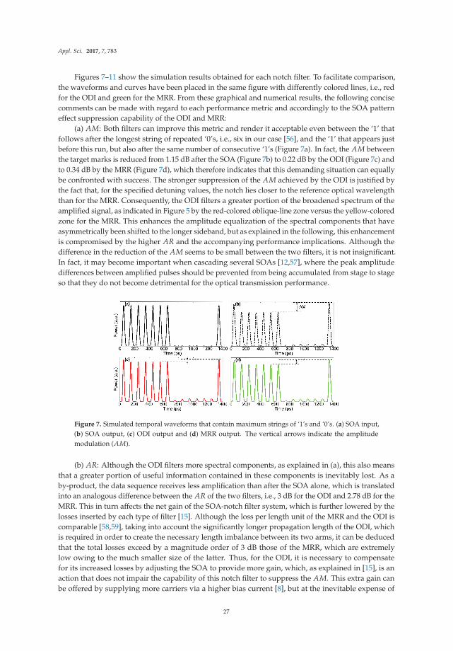
Appl. Sci. 2017, 7, 783
Figures 7–11 show the simulation results obtained for each notch filter. To facilitate comparison,the waveforms and curves have been placed in the same figure with differently colored lines, i.e., redfor the ODI and green for the MRR. From these graphical and numerical results, the following concisecomments can be made with regard to each performance metric and accordingly to the SOA patterneffect suppression capability of the ODI and MRR:
(a) AM: Both filters can improve this metric and render it acceptable even between the ‘1’ thatfollows after the longest string of repeated ‘0’s, i.e., six in our case [56], and the ‘1’ that appears justbefore this run, but also after the same number of consecutive ‘1’s (Figure 7a). In fact, the AM betweenthe target marks is reduced from 1.15 dB after the SOA (Figure 7b) to 0.22 dB by the ODI (Figure 7c) andto 0.34 dB by the MRR (Figure 7d), which therefore indicates that this demanding situation can equallybe confronted with success. The stronger suppression of the AM achieved by the ODI is justified bythe fact that, for the specified detuning values, the notch lies closer to the reference optical wavelengththan for the MRR. Consequently, the ODI filters a greater portion of the broadened spectrum of theamplified signal, as indicated in Figure 5 by the red-colored oblique-line zone versus the yellow-coloredzone for the MRR. This enhances the amplitude equalization of the spectral components that haveasymmetrically been shifted to the longer sideband, but as explained in the following, this enhancementis compromised by the higher AR and the accompanying performance implications. Although thedifference in the reduction of the AM seems to be small between the two filters, it is not insignificant.In fact, it may become important when cascading several SOAs [12,57], where the peak amplitudedifferences between amplified pulses should be prevented from being accumulated from stage to stageso that they do not become detrimental for the optical transmission performance.
Figure 7. Simulated temporal waveforms that contain maximum strings of ‘1’s and ‘0’s. (a) SOA input,(b) SOA output, (c) ODI output and (d) MRR output. The vertical arrows indicate the amplitudemodulation (AM).
(b) AR: Although the ODI filters more spectral components, as explained in (a), this also meansthat a greater portion of useful information contained in these components is inevitably lost. As aby-product, the data sequence receives less amplification than after the SOA alone, which is translatedinto an analogous difference between the AR of the two filters, i.e., 3 dB for the ODI and 2.78 dB for theMRR. This in turn affects the net gain of the SOA-notch filter system, which is further lowered by thelosses inserted by each type of filter [15]. Although the loss per length unit of the MRR and the ODI iscomparable [58,59], taking into account the significantly longer propagation length of the ODI, whichis required in order to create the necessary length imbalance between its two arms, it can be deducedthat the total losses exceed by a magnitude order of 3 dB those of the MRR, which are extremelylow owing to the much smaller size of the latter. Thus, for the ODI, it is necessary to compensatefor its increased losses by adjusting the SOA to provide more gain, which, as explained in [15], is anaction that does not impair the capability of this notch filter to suppress the AM. This extra gain canbe offered by supplying more carriers via a higher bias current [8], but at the inevitable expense of
27

Appl. Sci. 2017, 7, 783
increased power consumption. Accordingly, if insertion losses (IL) are included, the MRR allows theSOA-filter system to exhibit a higher net gain [15], i.e., 12.13 dB vs. 8.91 dB for the ODI.
(c) XC: The numerically-obtained values, 97% for the MRR and 93% for the ODI, indicate thatin both cases, the filtered pulse temporal waveform deviates only by 3% and 7%, respectively, from thatat the SOA input. This degree of matching implies that the Gaussian-like power profile of the input datapulses is strongly preserved at the filters’ output. This is visually confirmed in Figure 8a, which showsthat the envelope of an isolated data pulse maintains its original form. However, the time-bandwidthproduct at the output of both filters is over the minimum defined for Gaussian-shaped pulses [52],which means that the filtered pulses become chirped. The profile of this chirp, which is shownin Figure 8b, reflects the qualitative differences in the data pulse profiles of Figure 8a. More specifically,in the pulse rising part (region of 10–35 ps), the chirp declines to negative values, i.e., red chirp, butthis drop is more dominant for the ODI than for the MRR. This partly explains why the AMattainedwith the former notch filter is lower than that achieved with the latter. As the pulse continues totemporally evolve, the chirp is decreased more strongly for the ODI until we reach the pulse center,where its absolute magnitude becomes maximum. From this point onwards the situation is reversedand the chirp begins to incline with a slope that is sharper for the ODI than for the MRR. Consequently,and as explained in detail below, the chirp parameter is larger for the ODI, which has a negative impacton the transmission performance of this notch filter in the presence of fiber dispersion. Finally, as wemove off the pulse center and approach the pulse falling part (region of 65–80 ps), the chirp changessign and becomes positive, i.e., blue chirp, which, nevertheless, because of its different cause and timescale over its red chirp counterpart, is not of major concern with regard to the SOA pattern effectsuppression [31].
Figure 8. (a) Profile of isolated data pulse at ODI (red color) and MRR (green color) output in comparisonto SOA input (black color). (b) Corresponding chirp profile at ODI (red color) and MRR (green color).
28

Appl. Sci. 2017, 7, 783
(d) Q2-factor and associated metrics: (i) both filters enhance the IPDR and extend the SOA error-and distortion-free operation from the low saturation region (A in Figure 9) to the deep saturationregion (C in Figure 9), in which the SOA gain is decreased by more than 3 dB and 6 dB, respectively.This fact allows one to passively relax the stringent management [60,61] of the input power levels goinginto the SOA and hence of the degree of SOA gain saturation, which otherwise is required in order toallow SOAs to deliver unimpaired linear amplification functionality. This improvement is realizedfor both filters, as quantified by the increase of the peak input data power (Ppeak) by ΔP = 14 dB(assuming a maximum power of 10 dBm going into the SOA). Furthermore, at Ppeak � 6.6 dBm, whichheavily saturates the SOA [31], the Q2-factor is over its critical limit, which for the SOA alone fellshort by ΔQ2 = 4.3 dB. This is better achieved for the MRR than for the ODI, i.e., ΔQ2 = 2.87 dB andΔQ2 = 1 dB, respectively.
Figure 9. Q2-factor as a function of different peak input data powers for SOA alone (black color) andwith the connection of ODI (red color) and MRR (green color). The horizontal dotted line denotesthe lower limit set for the Q2-factor. The vertical dashed lines define the different saturation regions: A,low; B, medium; C, deep.
(ii) The MRR exhibits better tolerance to detuning offset than the ODI, which is an importantfeature as it obviates the need for resorting to electronic equalization [44]. In fact, Figure 10 showsthat the (negative) detuning of the MRR can be varied within 0.12 nm or equivalently by 50% furtherfor the data pulses wavelength modulation bandwidth [52] in the C-band and still keep the Q2-factoracceptable. The corresponding variation for the ODI is comparatively reduced by more than 50%,i.e., 0.05 nm, and hence is narrower, which may impose tighter requirements with regard to wavelengthlocking [62].
(iii) The MRR allows the amplified signal to propagate over a longer distance of SSMF withoutdispersion compensation than the ODI. This is shown in Figure 11, which has been obtainedby modeling the SSMF of typical attenuation coefficient 0.2 dB/km and dispersion parameter17 ps/nm/km by its low-pass equivalent field transfer function [63]. From this figure, it can beseen first that subject to chromatic dispersion, the maximum SSMF length is reduced to around20 km, as calculated from [64] (cf. Equation (1)) for intensity-modulated data pulses of a 100-psrepetition period and 27% duty cycle. Then, looking for the transmission range for which theQ2-factor is acceptable, we observe that the amplified signal can travel up to 12 km with theODI, while this span is extended to 15 km with the MRR. This length difference may seem small,but nevertheless, it corresponds to the reach of real short-haul fiber interconnection links and networks[65]. Moreover, the Q2-factor is well over its lower permissible bound for the MRR, while it ismuch closer to the borderline for the ODI, across the SSMF distance over which this metric remainsacceptable for both filters. These observations can be interpreted by referring to the instantaneousfrequency deviation, i.e., chirp, which inevitably accompanies a signal when directly amplified in an
29

Appl. Sci. 2017, 7, 783
SOA [26]. More specifically, suppressing the SOA pattern effect by means of optical notch filteringrelies on compensating for the chirp components, which are induced due to the irregular SOA gainvariation by the optical excitation, and converting them into amplitude changes that counteractthose after the SOA ([27], cf. Figure 4.18). Still, it is not possible to fully eliminate the SPM-inducednegative-magnitude chirp components, which are directly associated with the SOA pattern effect, butonly reduce the variations of their uneven peaks [31]. By calculating the maximum chirp variation, whichoccurs in the transition between the last ‘0’ in a run of spaces and the ‘1’ that immediately follows, wecan extract the chirp parameter at the filters’ output similarly to the numerical procedure describedin [66]. The value of this parameter is positive and is larger for the ODI than for the MRR. In thepresence of anomalous chromatic dispersion, this fact subsequently affects the pulse width of thechirped signal at the filters’ output [52]. Thus, after a short distance zone of pulse compression, pulsebroadening occurs, which is more significant for the ODI than for the MRR. This is reflected in theQ2-factor, which is smaller for the ODI and becomes worsened after propagation in a shorter SSMFlength (which is also smaller than that calculated from [64] (cf. Equation (1)) for the chirped-free signalcase). The obtained results are further supported by the so-called pseudo-eye diagrams (PEDs) [67],which are displayed at different points of the Q2-factor curves. Thus, both MRR and ODI restore theform of the PED, which has severely been degenerated into asymmetric sub-envelopes at the SOAoutput. This improvement is further quantified by the degree of eye opening (EOP) [68], which ishigher for the MRR than for the ODI, i.e., 91% vs. 87%, respectively, for transmission in the same fiberlength of 12 km.
Figure 10. Q2-factor for different detuning offset values for ODI (red color) and MRR (green color).The zero detuning refers to the case that the notch of the filters is located away from the data carrier byso many spectral units as defined in Figure 5.
30

Appl. Sci. 2017, 7, 783
Figure 11. Q2-factor vs. standard single-mode fiber (SSMF) distance for ODI (red color) and MRR(green color). The horizontal dotted line denotes the lower limit set for the Q2-factor.
The above improvements can be attributed to the different shape of the MRR and ODItransfer functions [69]. This difference affects the efficiency of the frequency-to-amplitude conversionmechanism, which is essential for suppressing the SOA pattern effect [44] and thus makes the MRRand ODI perform differently when employed as notch filters. Moreover, the comparatively betterperformance of the MRR can be justified from a qualitative standpoint by noting that the MRR exhibitshigher wavelength sensitivity than the ODI. In fact, for the MRR, this quantity is determined, andhence enhanced, by the finesse [70], which is a function of the coupling coefficient and internal loss [27]and accordingly can be flexibly adjusted. In contrast, the finesse of the ODI is very small, i.e., it equalsonly two [52], and therefore is fixed so that the design freedom is very limited. Physically, this happensdue to the different operating nature of the ODI and MRR, since in the former, only two constituentsof the input field interfere to produce an output, whilst in the MRR, the field experiences multiplecirculations before it leaves the resonant cavity [71]. Since in the first case, the interfering paths arefeeding forward, while in the second case there is a recirculating, feedback delay path, this difference,which is reflected on the polynomial form of the respective transfer functions, can also be expressedin signal processing terms. Accordingly, the ODI and MRR can be used not only as notch filters, but ingeneral as finite impulse response (FIR) and infinite impulse response (IIR) filters, respectively [72].FIR filters that exploit MRRs are also possible if sophisticated designs based on the combination ofmultiple such elements are adopted [73].
The values obtained for the employed performance metrics have been gathered in Table 1.
Table 1. Values of employed performance metrics.
Parameter ODI MRR
AM (dB) 0.22 0.34AR (dB) 3 2.78
Net gain (dB) 8.91 * 12.13XC (%) 93 97ΔP (dB) 14 14
ΔQ2 (dB) 1 2.87(negative) Detuning
offset (nm) 0.05 0.12
SSMF distance (km)w/o dispersioncompensation
12 15
EOP at 12 km (%) 87 91
* 3 dB insertion losses included.
31

Appl. Sci. 2017, 7, 783
6. ODI vs. MRR Qualitative Comparison
The key characteristics that the ODI- and MRR-based notch filters must exhibit in order to mitigatethe SOA pattern effect can be further assessed in a qualitative manner by considering the followingfunctional and technological issues:
(a) FSR:
The FSR of both filters can conveniently lie within the SOA wide gain spectrum enabled throughsuitable adjustment of the SOA active layer material composition [1]. For the ODI, the FSR can beadjusted either statically, by fixing the path length imbalance, which can be of the order of um, betweenthe ODI upper and lower arms, or dynamically, by using an optical delay line [32]. In the first case,a precise construction is required, but which is compensated by the reduction in footprint [74], whilein the second case, a wide range of relative delays can be offered with fine resolution at the expense ofa more bulky configuration [29]. For the MRR, the FSR can be readily set by choosing the MRR radius,which can be down to the micrometer scale using high index contrast waveguide materials [40,75]. Thisoffers the comparative benefit of ultra-compact total size at the expense of resorting to elaborate anddelicate microelectronic fabrication processes, which detracts from the global use of the specific scheme.
(b) Detuning:
The position of the notches relative to the input data carrier wavelength can be practically adjustedby exploiting effects such as thermo-optic. For this purpose, either active phase shifters are used tocontrol the phase bias in the ODI [58] or electrical heaters in the direct vicinity of the MRR to spectrallyshift its resonance [75]. This method is particularly efficient for materials of large positive thermo-opticcoefficients, such as silicon, since the required amount of detuning across the FSR can be achieved witha power supply of the order of mWs for both filters. On the other hand, the need for precise detuningis inherently more demanding for the ODI than for the MRR. This happens due to the different way bywhich the amount of phase shift required for efficiently suppressing the SOA pattern effect is obtained.Thus, for the ODI, this amount is acquired through one-way interference of a pair of delayed signalcopies, while for the MRR through periodic round-trips and resonant enhancement. Accordingly,the ODI operation is more sensitive to deviations from the condition of destructive interference, whichmust be tightly satisfied at its cross-wise output port [30], thus requiring special design [76,77].
(c) PNCR:
For the ODI the optimum PNCR can be achieved by adjusting the power splitting ratios ofthe optical couplers that form its two branches to be as symmetric as possible, i.e., as close as possibleto 3 dB [78]. In practice, in order to ensure a PNCR over 20 dB, the deviation from the perfect 3-dBsplitting ratio must be kept within 10% [29]. This tolerance is satisfiable with the coupling technologyemployed both in the fiber [79] and the waveguide [80] versions of the ODI.
Similarly, for the MRR, it is necessary to satisfy the condition of critical coupling, where the MRRfield transmission coefficient, r, and amplitude attenuation factor, l, are equal while tending tounity [40]. In effect, the PNCR exceeds 20 dB even if this matching is less than 3% perfect [81].The required matching can be accomplished by means of electrically-driven micro-electromechanicalsystem (MEMS) microactuators, which control the gap by deforming the straight waveguide againstthe ring [82]. The ring, waveguide and MEMS actuators can be patterned with standard opticallithography, thus rendering the fabrication of the whole system technologically feasible.
(d) Temperature sensitivity:
Although the strong thermo-optic effect of materials used as a platform for constructingthe considered filters allows one to efficiently tune them, it is also responsible for making them prone totemperature fluctuations [83]. This susceptibility may cause the bias point of the ODI and the resonancewavelength of the MRR to drift, which in turn could affect the process of suppressing the red-shifted
32

Appl. Sci. 2017, 7, 783
spectral components without significantly impairing the input data carrier and eventually leading totemperature-dependent performance degradation. Although it was numerically verified above that theMRR is, by its principle of operation, more tolerant to detuning offsets than the ODI, still, special caremust additionally be taken in order to enhance the resilience of both schemes to possible temperaturechanges while at the same time achieving this goal in an energy-efficient manner. To this aim, it hasbeen identified [83] that while athermal operation of the ODI is possible without any extra energyconsumption, there is no efficient passive solution to the problem for the MRR, as well. Furthermore,the exploitation of negative thermo-optic materials that could resolve the thermo-optic issue in astraightforward manner faces challenges with regard to compatibility with standard CMOS technologyand is the subject of intense research.
(e) Integration potential:
Both schemes are amenable to integration, which is highly desirable for keeping size and IL smallwhile enabling interconnection even at a small scale level. Thus, both are compatible with planarlight wave technology and can be co-packaged with the SOA in the same module in a monolithic(ODI) [80] or hybrid (MRR) [67,84] platform. Especially, the capability for co-packaging is rather crucialtowards compensating for the reduction in the amplified signal level due to notch filtering and hencefor extending transmission reach. Since the MRR can be made more compact than the ODI [83,85],the use of the former could be favored for mitigating the SOA pattern effect in applications wherespace availability is critical, as in the transmitter side for power boosting, especially of multiplewavelength outputs, or the receiver end for power preamplification, or within intra-data center opticallinks [85]. On the other hand, it should be noted that both filters are compatible with standard CMOS(complementary metal-oxide-semiconductor) processing in silicon photonics platform [85,86] andhence can leverage the benefits that accompany this mature fabrication technology.
(f) Multi-wavelength operation:
Both filters can mitigate the SOA pattern effect induced on wavelength-division-multiplexed(WDM) data inputs, for all channels simultaneously [87]. The specific potential is enabled bythe periodic spectral response of these filters and can be exploited provided that the center wavelengthsof the different input data are spaced apart by integer multiples of the FSR [21,58]. In this case,the amplitude equalization can be realized by means of a single such optical notch filter, which isattractive from an economical point of view, since the cost of using the device can be shared among themultiple served data inputs and remain affordable with the increase of channel count [62].
Furthermore, the two types of filters can be discriminated, with regard to their efficiency, toenhance the amplitude uniformity of multiple SOA amplified data-carrying channels, by the amountof the achieved FSR, which is compared against the wavelength separation between adjacent channelsin real deployed WDM communication systems. Thus, for the ODI, the FSR that corresponds toa relative delay of ∼10 ps between its two arms is almost the standardized dense WDM grid spacingof 0.8 nm at around a 1550-nm carrier wavelength. On the contrary, the MRR μm radial size resultsin an FSR that is an order of magnitude higher and accordingly more suitable for coarse WDMpurposes. Another option is to cascade several MRRs of different radii along the same waveguidebus [88]. This allows one to accommodate more data wavelengths impaired by the SOA pattern effectand with a more dense spacing than for a single MRR [33], at the expense of a larger footprint and amore complex configuration. On the other hand, in WDM systems of some given interchannel spacingand spectral width, a single MRR can support numerous channels in a much more flexible mannerthan a single ODI. In fact, this capability critically depends on one filter’s finesse, which, as previouslymentioned, can be flexibly adjusted for the MRR, whereas it is very low and fixed for the ODI.Furthermore, the sharper spectral selectivity of the MRR allows the latter to better handle variations inthe channel positions and compensate for possible misalignments against notches. This further allowsone to use uncooled, i.e., non-temperature-controlled, single-mode lasers, which is an attractive feature
33

Appl. Sci. 2017, 7, 783
from a cost and operational perspective [8]. In contrast, these functional requirements can be metwith the ODI only if multiple ODI stages are concatenated [52], which, along with the aforementionedinevitable compromises associated with the employment of chains of filters, comes at the additionalcost of extra losses.
(g) Tunability:
The tunability of each type of filter can be assessed against bandwidth tunability andwavelength tunability [89]. For the first ability, we can calculate its minimum, which can be donein a straightforward manner by using the analytic formulas that quantify it. These are given from [52]FWHMODI = FSRODI/2 for the ODI and FWHMMRR = λ2
amp(1 − rl)/(2π2ne f f R√
rl) [75]. Recallnow that in order to prevent the filtering action that suppresses the SOA pattern effect on the datapulses from distorting the latter, the ODI delay should not exceed 10 ps [31], while the MRR radiusshould not be larger than 42 um [33]. Then, substituting these maximum values together withλamp = 1550 nm, r = l = 0.95 and ne f f = 1.41 in the above expressions of the FWHM, it can befound that FWHMODI ≥ 0.4 nm and FWHMMRR ≥ 21 nm. For the second ability, on the other hand,we have shown from Figure 10 that the wavelength offset of the MRR is allowed to be larger than thatof the ODI while maintaining an acceptable Q2-factor. Thus, in both cases, the numerically-obtainednumbers suggest that the MRR filter is better tunable for the target application of SOA patterneffect compensation.
Table 2 summarizes the qualitative comparison of the MRR and ODI key characteristics. Note thatthis comparison is not absolute in the sense that each filter has its own special features, which mayrender it more suitable than the other for exploitation in SOA direct amplification applications with asuppressed pattern effect.
34

Appl. Sci. 2017, 7, 783
Table 2. Qualitative comparison of MRR and ODI key characteristics.
Characteristic MRR ODI
Free SpectralRange (FSR)
Width Coarse Dense
Adjustment Rather fine (radius) Fine (path length imbalance) orbulky (optical delay line)
Multi-wavelength Operation Yes Yes
(i) ITU -Grid
Difficult for DWDM since itrequires cascading; is
compromised by increasedfootprint and complexity
Easy for DWDM
(ii) fixed interchannel spacingand spectral width
Yes, easy with single MRRowing to high and controllable
finesse
Yes, difficult due to low andfixed finesse
(iii) handling of variations inchannel positions
Yes, straightforward owing tosharp spectral selectivity
Yes, requires to concatenatemultiple stages at the cost of
increased complexity andinsertion losses
Detuning
Feasibility Yes, thermo-optic effect with mWs/FSR
Mechanism Relaxed (periodic round-tripsand resonant enhancement) Tight (one-way interference)
Precision Normal Demanding
Tolerance High Medium
Tunability Yes, high Yes, medium
Peak-to-NotchContrast Ratio(PNCR)
Magnitude High (>20 dB)
Operating Condition Demanding (critical coupling) Normal (branching couplerssplitting ratio)
AdjustmentComplicated (electrically
driving MEMS to control gapbetween bus and ring)
Simple (varying powersplitting ratio)
Tolerance
Tight (matching of fieldtransmission coefficient andamplitude attenuation factor
within 3%)
Relaxed (Within 10% of 3-dBpower splitting ratio)
TemperatureSensitivity
Yes, high negative TOC material,but still not compatibility with
standard CMOS technology
Yes, athermal operation withoutextra energy consumption
IntegrationPotential
Compatibility with planar lightwave technology Yes Yes
Co-packaging Platformwith SOA Yes (hybrid) Yes (monolithic)
Device
Size and footprint Ultra-compact Compact or bulk
Fabrication, (materials,techniques, processes) Well-developed Established
CMOS Compatible Yes Yes
Cost Affordable (single channel amplification in SOA),Shared (multiple channel amplification in SOA)
Commercial availability Yes, increasing Yes, widespread
7. Conclusions
In conclusion, we have presented a theoretical analysis and benchmarking of two basic opticalnotch filters employed to compensate for the pattern effect that manifests in an SOA due to theirregular perturbation of the SOA gain dynamics by a directly-amplified data-modulated opticalsignal. After following a rational procedure based on the satisfaction of signal amplitude equalizationconditions, we extracted values of the critical operating parameters, which enable a fair comparison ofthese filters through evaluating them against appropriately-adopted figures-of-merit. In this manner,
35

Appl. Sci. 2017, 7, 783
we have specified the points where the considered filters perform better due to their different principlesof operation and associated spectral responses. The obtained results denote that, with the exception oflarger amplitude modulation, which however is well compensated by the other comparative realizedimprovements, the MRR outperforms the ODI in most employed metrics. This conclusion is furthersupported by the comparison made between the filters from a functional and technical side. In fact,the MRR exhibits several attractive key characteristics, which, along with its capability to confrontthe SOA pattern effect, allows it to favorably compete against the well-established ODI. This factconstructively broadens the technological options that are available for addressing the target problem.Furthermore, it indicates that, since there is no absolute criterion for preferring one filter to the other,making a selection should be done in such a way so that it best suits the particular needs of a lightwave link or network where SOA direct amplification with a suppressed pattern effect is essential.To this end, each filter should judiciously be exploited while making the necessary trade-offs accordingto its inherent performance advantages and disadvantages.
Author Contributions: Zoe V. Rizou conducted the simulation and interpreted the obtained results;Kyriakos E. Zoiros conceived the initial idea and wrote the paper; Antonios Hatziefremidis reviewed the resultsand the manuscript.
Conflicts of Interest: The authors declare no conflict of interest.
References
1. Zimmerman, D.R.; Spiekman, L.H. Amplifiers for the masses: EDFA, EDWA, and SOA amplets for metroand access applications. J. Lightwave Technol. 2004, 22, 63–70.
2. Bonk, R.; Schmuck, H.; Poehlmann, W.; Pfeiffer, T. Beneficial OLT transmitter and receiver concepts forNG-PON2 using semiconductor optical amplifiers. J. Opt. Commun. Netw. 2015, 7, A467–A473.
3. Connelly, M.J. Semiconductor Optical Amplifiers; Kluwer Academic Publishers: Dordrecht, The Netherlands,2002; Chapter 6.
4. Mørk, J.; Nielsen, M.L.; Berg, T.W. The dynamics of semiconductor optical amplifiers: Modeling andapplications. Opt. Photonics News 2003, 14, 42–48.
5. Kamelian. Applications Note No. 0001 “Semiconductor Optical Amplifiers (SOAs) as Power Boosters” and No.0002 “Semiconductor Optical Amplifiers (SOAs) as Pre-Amplifiers”. Available online: http://www.kamelian.com (accessed on 12 July 2017).
6. Spiekman, L.H.; Wiesenfeld, J.; Gnauck, A.; Garrett, L.; Van Den Hoven, G.; Van Dongen, T.; Sander-Jochem, M.;Binsma, J. Transmission of 8 DWDM channels at 20 Gb/s over 160 Km of standard fiber using a cascade ofsemiconductor optical amplifiers. IEEE Photonics Technol. Lett. 2000, 12, 717–719.
7. Udvary, E.; Berceli, T. Semiconductor optical amplifier for detection function in radio over fiber systems.J. Lightwave Technol. 2008, 26, 2563–2570.
8. Porto, S.; Antony, C.; Ossieur, P.; Townsend, P.D. An upstream reach-extender for 10 Gb/s PON applicationsbased on an optimized semiconductor amplifier cascade. Opt. Express 2012, 20, 186–191.
9. Yiannopoulos, K.; Sagias, N.C.; Boucouvalas, A.C. Fade mitigation based on semiconductor optical amplifiers.J. Lightwave Technol. 2013, 31, 3621–3630.
10. Miao, W.; Luo, J.; Di Lucente, S.; Dorren, H.; Calabretta, N. Novel flat datacenter network architecture basedon scalable and flow-controlled optical switch system. Opt. Express 2014, 22, 2465–2472.
11. Schmuck, H.; Bonk, R.; Poehlmann, W.; Haslach, C.; Kuebart, W.; Karnick, D.; Meyer, J.; Fritzsche, D.; Weis, E.;Becker, J.; et al. Demonstration of an SOA-assisted open metro-access infrastructure for heterogeneousservices. Opt. Express 2014, 22, 737–748.
12. Pato, S.V.; Meleiro, R.; Fonseca, D.; Andre, P.; Monteiro, P.; Silva, H. All-optical burst-mode power equalizerbased on cascaded SOAs for 10-Gb/s EPONs. IEEE Photonics Technol. Lett. 2008, 20, 2078–2080.
13. Manning, R.; Ellis, A.; Poustie, A.; Blow, K. Semiconductor laser amplifiers for ultrafast all-optical signalprocessing. J. Opt. Soc. Am. B 1997, 14, 3204–3216.
14. Zoiros, K.; Chasioti, R.; Koukourlis, C.; Houbavlis, T. On the output characteristics of a semiconductor opticalamplifier driven by an ultrafast optical time division multiplexing pulse train. Optik 2007, 118, 134–146.
36

Appl. Sci. 2017, 7, 783
15. Rizou, Z.V.; Zoiros, K.E.; Hatziefremidis, A.; Connelly, M.J. Design analysis and performance optimizationof a Lyot filter for semiconductor optical amplifier pattern effect suppression. J. Sel. Top. Quantum Electron.2013, 19, 1–9.
16. Bonk, R.; Huber, G.; Vallaitis, T.; Koenig, S.; Schmogrow, R.; Hillerkuss, D.; Brenot, R.; Lelarge, F.; Duan, G.H.;Sygletos, S.; et al. Linear semiconductor optical amplifiers for amplification of advanced modulation formats.Opt. Express 2012, 20, 9657–9672.
17. Bogoni, A.; Potì, L.; Ghelfi, P.; Scaffardi, M.; Porzi, C.; Ponzini, F.; Meloni, G.; Berrettini, G.; Malacarne, A.;Prati, G. OTDM-based optical communications networks at 160 Gbit/s and beyond. Opt. Fiber Technol.2007, 13, 1–12.
18. Winzer, P.J.; Essiambre, R.J. Advanced modulation formats for high-capacity optical transport networks.J. Lightwave Technol. 2006, 24, 4711–4728.
19. Mecozzi, A.; Mørk, J. Saturation induced by picosecond pulses in semiconductor optical amplifiers. J. Opt.Soc. Am. B 1997, 14, 761–770.
20. Inoue, K. Optical filtering technique to suppress waveform distortion induced in a gain-saturatedsemiconductor optical amplifier. Electron. Lett. 1997, 33, 885–886.
21. Watanabe, T.; Yasaka, H.; Sakaida, N.; Koga, M. Waveform shaping of chirp-controlled signal bysemiconductor optical amplifier using Mach-Zehnder frequency discriminator. IEEE Photonics Technol. Lett.1998, 10, 1422–1424.
22. Yu, J.; Jeppesen, P. Increasing input power dynamic range of SOA by shifting the transparent wavelength oftunable optical filter. J. Lightwave Technol. 2001, 19, 1316–1325.
23. Wong, C.; Tsang, H. Reduction of bit-pattern dependent errors from a semiconductor optical amplifier usingan optical delay interferometer. Opt. Commun. 2004, 232, 245–249.
24. Dong, J.; Zhang, X.; Wang, F.; Hong, W.; Huang, D. Experimental study of SOA-based NRZ-to-PRZconversion and distortion elimination of amplified NRZ signal using spectral filtering. Opt. Commun.2008, 281, 5618–5624.
25. Hussain, K.; Pradhan, R.; Datta, P. Patterning characteristics and its alleviation in high bit-rate amplificationof bulk semiconductor optical amplifier. Opt. Quantum Electron. 2010, 42, 29–43.
26. Agrawal, G.P.; Olsson, N.A. Self-phase modulation and spectral broadening of optical pulses insemiconductor laser amplifiers. IEEE J. Quantum Electron. 1989, 25, 2297–2306.
27. Wang, J. Pattern Effect Mitigation Techniques for All-Optical Wavelength Converters Based on SOAs.Ph.D. Thesis, Karlsruhe Institute of Technology, Karlsruhe, Germany, 2008.
28. Zoiros, K.E.; O’Riordan, C.; Connelly, M.J. Semiconductor optical amplifier pattern effect suppression usinga birefringent fiber loop. IEEE Photonics Technol. Lett. 2010, 22, 221–223.
29. Rizou, Z.; Zoiros, K.; Hatziefremidis, A.; Connelly, M. Performance tolerance analysis of birefringent fiberloop for semiconductor optical amplifier pattern effect suppression. Appl. Phys. B Lasers Opt. 2015, 119,247–257.
30. Zoiros, K.E.; Siarkos, T.; Koukourlis, C.S. Theoretical analysis of pattern effect suppression in semiconductoroptical amplifier utilizing optical delay interferometer. Opt. Commun. 2008, 281, 3648–3657.
31. Zoiros, K.E.; Rizou, Z.V.; Connelly, M.J. On the compensation of chirp induced from semiconductor opticalamplifier on RZ data using optical delay interferometer. Opt. Commun. 2011, 284, 3539–3547.
32. Zoiros, K.E.; Janer, C.L.; Connelly, M.J. Semiconductor optical amplifier pattern effect suppression forreturn-to-zero data using an optical delay interferometer. Opt. Eng. 2010, 49, 1–4.
33. Rizou, Z.; Zoiros, K.; Hatziefremidis, A. Semiconductor optical amplifier pattern effect suppression withpassive single microring resonator-based notch filter. Opt. Commun. 2014, 329, 206–213.
34. Katz, O.; Malka, D. Design of novel SOI 1 × 4 optical power splitter using seven horizontally slottedwaveguides. Photonics Nanostruct. 2017, 25, 9–13.
35. Malka, D.; Peled, A. Power splitting of 1 × 16 in multicore photonic crystal fibers. Appl. Surf. Sci. 2017,417, 34–39.
36. Ben Zaken, B.B.; Zanzury, T.; Malka, D. An 8-channel wavelength MMI demultiplexer in slot waveguidestructures. Materials 2016, 9, 881.
37. Malka, D.; Sintov, Y.; Zalevsky, Z. Design of a 1 × 4 silicon-alumina wavelength demultiplexer based onmultimode interference in slot waveguide structures. J. Opt. 2015, 17, 125702.
37

Appl. Sci. 2017, 7, 783
38. Malka, D.; Sintov, Y.; Zalevsky, Z. Fiber-laser monolithic coherent beam combiner based on multicorephotonic crystal fiber. Opt. Eng. 2015, 54, 011007.
39. Wong, C.; Tsang, H. Filtering directly modulated laser diode pulses with a Mach-Zehnder optical delayinterferometer. Electron. Lett. 2004, 40, 938–940.
40. Rabus, D.G. Integrated Ring Resonators: The Compendium; Spring: Berlin, Germany, 2007.41. Sumetsky, M. Optimization of resonant optical sensors. Opt. Express 2007, 15, 17449–17457.42. Ruege, A.C. Electro-Optic Ring Resonators in Integrated Optics for Miniature Electric Field Sensors.
Ph.D. Thesis, The Ohio State University, Columbus, OH, USA, 2001.43. Nielsen, M.L.; Mørk, J. Bandwidth enhancement of SOA-based switches using optical filtering: Theory and
experimental verification. Opt. Express 2006, 14, 1260–1265.44. Udvary, E. Off-set filtering effect in SOA based optical access network. Radioengineering 2016, 25, 26–33.45. Yu, H.Y.; Mahgerefteh, D.; Cho, P.S.; Goldhar, J. Optimization of the frequency response of a semiconductor
optical amplifier wavelength converter using a fiber Bragg grating. J. Lightwave Technol. 1999, 17, 308–315.46. Nielsen, M.L.; Mørk, J.; Suzuki, R.; Sakaguchi, J.; Ueno, Y. Theoretical and experimental study of fundamental
differences in the noise suppression of high-speed SOA-based all-optical switches. Opt. Express 2005,13, 5080–5086.
47. Nielsen, M.L. Experimental and Theoretical Investigation of Semiconductor Optical Amplifier (SOA) BasedAll-Optical Switches. Ph.D. Thesis, Technical University of Denmark, Kongens Lyngby, Denmark, 2004.
48. Rizou, Z.V.; Zoiros, K.E. Performance analysis and improvement of semiconductor optical amplifier directmodulation with assistance of microring resonator notch filter. Opt. Quantum Electron. 2017, 3, 1–21.
49. Vardakas, J.S.; Zoiros, K.E. Performance investigation of all-optical clock recovery circuit based onFabry-Pérot filter and semiconductor optical amplifier assisted Sagnac switch. Opt. Eng. 2007, 46, 1–21.
50. Gutiérrez-Castrejón, R.; Filios, A. Pattern-effect reduction using a cross-gain modulated holding beam insemiconductor optical in-line amplifier. J. Lightwave Technol. 2006, 24, 4912–4917.
51. Yan, S.; Zhang, Y.; Dong, J.; Zheng, A.; Liao, S.; Zhou, H.; Wu, Z.; Xia, J.; Zhang, X. Operation bandwidthoptimization of photonic differentiators. Opt. Express 2015, 23, 18925–18936.
52. Agrawal, G.P. Fiber-Optic Communication Systems, 3rd ed.; Wiley: New York, NY, USA, 2002.53. Bonk, R.; Vallaitis, T.; Guetlein, J.; Meuer, C.; Schmeckebier, H.; Bimberg, D.; Koos, C.; Freude, W.; Leuthold, J.
The input power dynamic range of a semiconductor optical amplifier and its relevance for access networkapplications. IEEE Photonics J. 2011, 3, 1039–1053.
54. Vacondio, F.; Ghazisaeidi, A.; Bononi, A.; Rusch, L.A. Low-complexity compensation of SOA nonlinearityfor single-channel PSK and OOK. J. Lightwave Technol. 2010, 28, 277–288.
55. Xu, J.; Zhang, X.; Mørk, J. Investigation of patterning effects in ultrafast SOA-based optical switches. IEEE J.Quantum Electron. 2010, 46, 87–94.
56. MacWilliams, F.J.; Sloane, N.J. Pseudo-random sequences and arrays. Proc. IEEE 1976, 64, 1715–1729.57. Singh, S.; Kaler, R. Transmission performance of 20 × 10 Gb/s WDM signals using cascaded optimized
SOAs with OOK and DPSK modulation formats. Opt. Commun. 2006, 266, 100–110.58. Bhardwaj, A.; Doerr, C.R.; Chandrasekhar, S.; Stulz, L.W. Reduction of nonlinear distortion from a
semiconductor optical amplifier using an optical equalizer. IEEE Photonics Technol. Lett. 2004, 16, 921–923.59. Niehusmann, J.; Vörckel, A.; Bolivar, P.H.; Wahlbrink, T.; Henschel, W.; Kurz, H. Ultrahigh-quality-factor
silicon-on-insulator microring resonator. Opt. Lett. 2004, 29, 2861–2863.60. Fujiwara, M.; Imai, T.; Taguchi, K.; Suzuki, K.I.; Ishii, H.; Yoshimoto, N. Field trial of 100-km reach
symmetric-rate 10 G-EPON system using automatic level controlled burst-mode SOAs. J. Lightwave Technol.2013, 31, 634–640.
61. Porzi, C.; Kado, Y.; Shimizu, S.; Maruta, A.; Wada, N.; Bogoni, A.; Kitayama, K.I. Simple uplink SOA patterneffects compensation for reach-extended 10 G-EPONs. IEEE Photonics. Technol. Lett. 2014, 26, 165–168.
62. Kim, H. 10-Gb/s operation of RSOA using a delay interferometer. IEEE Photonics Technol. Lett. 2010, 22,1379–1381.
63. Elrefaie, A.F.; Wagner, R.E.; Atlas, D.; Daut, D. Chromatic dispersion limitations in coherent light wavetransmission systems. J. Lightwave Technol. 1988, 6, 704–709.
64. Forghieri, F.; Prucnal, P.; Tkach, R.; Chraplyvy, A.R. RZ versus NRZ in nonlinear WDM systems.IEEE Photonics Technol. Lett. 1997, 9, 1035–1037.
38

Appl. Sci. 2017, 7, 783
65. Levaufre, G.; Le Liepvre, A.; Jany, C.; Accard, A.; Kaspar, P.; Brenot, R.; Make, D.; Lelarge, F.; Olivier, S.;Malhouitre, S.; et al. Hybrid III-V/silicon tunable laser directly modulated at 10 Gbit/s for shortreach/access networks. In Proceedings of the European Conference on Optical Communication, Cannes,France, 21–25 September 2014.
66. Dubé-Demers, R.; LaRochelle, S.; Shi, W. Ultrafast pulse-amplitude modulation with a femtojoule siliconphotonic modulator. Optica 2016, 3, 622–627.
67. Gutiérrez-Castrejón, R.; Occhi, L.; Schares, L.; Guekos, G. Recovery dynamics of cross-modulated beamphase in semiconductor amplifiers and applications to all-optical signal processing. Opt. Commun. 2001,195, 167–177.
68. Gayen, D.K.; Chattopadhyay, T.; Zoiros, K.E. All-optical D flip-flop using single quantum-dot semiconductoroptical amplifier assisted Mach-Zehnder interferometer. J. Comput. Electron. 2015, 14, 129–138.
69. Zhang, L.; Li, Y.; Song, M.; Beausoleil, R.G.; Willner, A.E. Data quality dependencies in microring-basedDPSK transmitter and receiver. Opt. Express 2008, 16, 5739–5745.
70. Tazawa, H.; Kuo, Y.H.; Dunayevskiy, I.; Luo, J.; Jen, A.K.Y.; Fetterman, H.R.; Steier, W.H. Ring resonator-basedelectrooptic polymer traveling-wave modulator. J. Lightwave Technol. 2006, 24, 3514–3519.
71. Ye, T.; Cai, X. On power consumption of silicon-microring-based optical modulators. J. Lightwave Technol.2010, 28, 1615–1623.
72. Madsen, C.K.; Zhao, J.H. Optical Filter Design and Analysis: A Signal Processing Approach; John Wiley & Sons,Inc.: New York, NY, USA, 1999; pp. 1–5.
73. Malka, D.; Cohen, M.; Turkiewicz, J.; Zalevsky, Z. Optical micro-multi-racetrack resonator filter based onSOI waveguides. Photonics Nanostruct. 2015, 16, 16–23.
74. Wu, Q.; Zhang, H.; Fu, X.; Yao, M. Spectral encoded photonic analog-to-digital converter based on cascadedunbalanced MZMs. IEEE Photonics Technol. Lett. 2009, 21, 224–226.
75. Bogaerts, W.; De Heyn, P.; Van Vaerenbergh, T.; De Vos, K.; Kumar Selvaraja, S.; Claes, T.; Dumon, P.;Bienstman, P.; Van Thourhout, D.; Baets, R. Silicon microring resonators. Laser Photonics Rev. 2012, 6, 47–73.
76. Kim, T.Y.; Hanawa, M.; Kim, S.J.; Hann, S.; Kim, Y.H.; Han, W.T.; Park, C.S. Optical delay interferometerbased on phase shifted fiber Bragg grating with optically controllable phase shifter. Opt. Express 2006, 14,4250–4255.
77. Li, J.; Worms, K.; Maestle, R.; Hillerkuss, D.; Freude, W.; Leuthold, J. Free-space optical delay interferometerwith tunable delay and phase. Opt. Express 2011, 19, 11654–11666.
78. Su, T.; Zhang, M.; Chen, X.; Zhang, Z.; Liu, M.; Liu, L.; Huang, S. Improved 10-Gbps uplink transmission inWDM-PON with RSOA-based colorless ONUs and MZI-based equalizers. Opt. Laser Technol. 2013, 51, 90–97.
79. Luo, Z.C.; Cao, W.J.; Luo, A.P.; Xu, W.C. Polarization-independent, multifunctional all-fiber comb filter usingvariable ratio coupler-based Mach-Zehnder interferometer. J. Lightwave Technol. 2012, 30, 1857–1862.
80. Bhardwaj, A.; Sauer, N.; Buhl, L.; Yang, W.; Zhang, L.; Neilson, D.T. An InP-based optical equalizermonolithically integrated with a semiconductor optical amplifier. IEEE Photonics Technol. Lett. 2007, 19,1514–1516.
81. Absil, P.; Hryniewicz, J.; Little, B.; Wilson, R.; Joneckis, L.; Ho, P.T. Compact microring notch filters.IEEE Photonics Technol. Lett. 2000, 12, 398–400.
82. Lee, M.C.; Wu, M.C. MEMS-actuated microdisk resonators with variable power coupling ratios.IEEE Photonics Technol. Lett. 2005, 17, 1034–1036.
83. Zhou, Z.; Yin, B.; Deng, Q.; Li, X.; Cui, J. Lowering the energy consumption in silicon photonic devices andsystems. Photonics Res. 2015, 3, B28–B46.
84. Kaspar, P.; Brenot, R.; Le Liepvre, A.; Accard, A.; Make, D.; Levaufre, G.; Girard, N.; Lelarge, F.; Duan, G.H.;Pavarelli, N.; et al. Packaged hybrid III-V/silicon SOA. In Proceedings of the European Conference onOptical Communication, Cannes, France, 21–25 September 2014.
85. Li, Y.; Zhang, Y.; Zhang, L.; Poon, A.W. Silicon and hybrid silicon photonic devices for intra-datacenterapplications: State of the art and perspectives. Photonics Res. 2015, 3, B10–B27.
86. Gunn, C. CMOS photonics for high-speed interconnects. IEEE Micro 2006, 26, 58–66.87. Tan, H.N.; Matsuura, M.; Kishi, N. Enhancement of input power dynamic range for multiwavelength
amplification and optical signal processing in a semiconductor optical amplifier using holding beam effect.J. Lightwave Technol. 2010, 28, 2593–2602.
39

Appl. Sci. 2017, 7, 783
88. Padmaraju, K.; Bergman, K. Resolving the thermal challenges for silicon microring resonator devices.Nanophotonics 2014, 3, 269–281.
89. Ding, Y.; Pu, M.; Liu, L.; Xu, J.; Peucheret, C.; Zhang, X.; Huang, D.; Ou, H. Bandwidth and wavelength-tunable optical bandpass filter based on silicon microring-MZI structure. Opt. Express 2011, 19, 6462–6470.
c© 2017 by the authors. Licensee MDPI, Basel, Switzerland. This article is an open accessarticle distributed under the terms and conditions of the Creative Commons Attribution(CC BY) license (http://creativecommons.org/licenses/by/4.0/).
40

applied sciences
Article
Estimation of the Performance Improvementof Pre-Amplified PAM4 Systems When UsingMulti-Section Semiconductor Optical Amplifiers
Seán P. Ó Dúill *, Pascal Landais and Liam P. Barry
Radio and optics research laboratory, School of Electronic Engineering,Dublin City University, Dublin 9 D09 W6Y4, Ireland; [email protected] (P.L.); [email protected] (L.P.B.)* Correspondence: [email protected]; Tel.: +353-1-700-5869
Received: 1 August 2017; Accepted: 31 August 2017; Published: 5 September 2017
Featured Application: Multi-section semiconductor optical amplifiers are known to have superior
noise and gain saturation performances compared to regular single section semiconductor
optical amplifiers. In this paper, we estimate the performance benefit of using multi-section
semiconductor optical amplifiers as pre-amplifiers for short range optical communication links
within datacenters.
Abstract: Multi-section semiconductor optical amplifiers (SOA) have been shown to have superiornoise and linearity performance compared with single section SOAs. We show how to createa simplified numerical model for multi-section SOAs that is suitable for optical communicationsystem simulations and use that model to investigate the amplification performance of 56 Gbit/sfour-level pulse amplitude modulation signals. We find that a multi-section SOA could provide animprovement in input power dynamic range exceeding 3 dB compared to a single section SOA thathas the same unsaturated gain.
Keywords: semiconductor optical amplifier; pulse amplitude modulation; noise
1. Introduction
There have been tremendous advances in the information carrying capacity of opticalcommunication systems within the past decade, with the optical techniques for communicationnow migrating to intra-datacenter communication [1,2]. The growth of stored data within datacentersand the necessity to retrieve this data is driving the requirement for cost-effective, higher capacityintra-datacenter interconnects to 400 Gbit/s and the data modulation format is evolving towardsfour-level pulse amplitude modulation (PAM4) that carries two bits per every transmitted symbol [2].Figure 1a presents a simplified schematic of a data connection between two clusters of racks ina datacenter where optoelectronic transponders and optical fiber form the basic communication link.Already, a bank of eight externally modulated lasers using electro-absorption modulators to deliver400 Gbit/s links on a single fiber can be offered with 28 Gbaud PAM4 offering a raw data rate of56 Gbit/s per wavelength [3].
Semiconductor optical amplifiers (SOA) are low cost, highly integratable amplifiers that may findtwo roles within intra-datacenter communication. Firstly, optical switches with light paths defined byactivated SOAs have been demonstrated [4,5] and could provide additional switching functionality inan optical-domain switching layer. Secondly, SOAs are being given serious consideration to also playa role as pre-amplifiers for PAM4 signals as reach extenders or to overcome inevitable insertion lossesof an optical switch as shown in Figure 1b [6,7]. Usually, SOAs suffer from a relatively high noisefigure (NF) which limits the minimum signal power that can be reliably amplified to a few tens of μW;
Appl. Sci. 2017, 7, 908; doi:10.3390/app7090908 www.mdpi.com/journal/applsci41

Appl. Sci. 2017, 7, 908
SOAs also suffer from low gain saturation power (the order of 10 mW) which distorts the amplifiedsignal even when the average input signal power is of the order of hundreds of microwatts [8,9].
Figure 1. (a) Simplified schematic showing communication between two clusters of racks in a datacenter.The transponders use externally modulated lasers (EML) to communicate at up to 400 Gbit/s betweenthe top of the rack aggregators (ToR Agg.); (b) Proposed use of semiconductor optical amplifiers (SOA)as a pre-amplifier to overcome losses within an optical switch. Eyediagrams of the simulated PAM4signals are shown, in (b) a slightly distorted eyediagram due to the SOA nonlinearities are shown.
The NF and saturation power of SOAs can be improved by subdividing the amplifier into separatesections and applying a different bias current to each subsection [10]. The concept of a multi-sectionSOA [10] is shown in Figure 2. In Figure 2a, for a single-section SOA, a large DC bias current isapplied to the SOA resulting in equal carrier injection being applied along the entire length of theSOA. For the multi-contact SOA, the SOA is subdivided into smaller sections with each section biasedindependently. The SOA is operated with favorable current biasing arrangements, whereby a strongerbias current is applied towards the output facet allowing for an improvement of the effective NFand increase in the effective saturation power relative to single-section SOAs [10–12]. This favorablebiasing current arrangement can be done without increasing the overall injected current and hencekeeping the power consumption constant. In separate works, regarding reflective SOAs (RSOA),with the RSOA subdivided into two subsections was found to have improved the direct modulationelectro-optic response of the RSOA [13]. To date, no study (neither experimental nor numerical) hasbeen performed on investigating the benefits of amplifying information-carrying modulated opticalsignals using multi-section SOAs, only the NF and saturation powers have been measured and/orcalculated [10–12]. In addition, a simplified numerical model for multi-section SOAs has not yetbeen developed that would allow estimating the amplification performance of modulated signalsin multi-section SOAs.
In this paper, we show how to create a simplified multi-section SOA model and use that modelto evaluate the amplification performance of multi-section SOAs, and as comparison to conventionalsingle-section SOAs for 28 Gbaud PAM4 signals. We are modifying our simplified SOA modelin [14] to consider multi-section SOAs. We find that in order to replicate the experimental resultsfor amplification of PAM4 signals using SOAs in [15], we need only consider amplified spontaneousemission (ASE) noise generated in the SOA and thermal noise in an optical receiver, and we achievesimilar bit-error rate (BER) performance to experimental 28 Gbaud PAM4 systems [15]. The inputpower dynamic range (IPDR) is an important metric for amplified systems using SOAs [8], because theIPDR indicates the useful input power range over which signals can be amplified and the data retrievedwithout error [8]. We show that a multi-section SOA could improve the IPDR by more than 3 dBrelative to the IPDR of a similar gain single-section SOA. The results, from this simple system simulatorfor multi-section SOAs, motivate the further experimental investigation of multi-section SOAs fordatacom applications.
42

Appl. Sci. 2017, 7, 908
Figure 2. (a) Simplified schematic of a travelling wave single-section SOA where the populationinversion is created by biasing the whole amplifier with a single current; (b) Multi-section SOA, the biascurrents to the smaller amplifier sections are independently set. The multi-section biasing arrangementcreates an SOA with improved noise and gain saturation performances compared to the case in (a).
2. Numerical Simulator
We create an optical field, E, that is normalised such that |E|2 represents the optical power.The four level 28 Gbaud PAM4 signal is encoded within the optical power domain. We set the extinctionratio between the strongest and weakest levels of the PAM4 signal to be 8 dB. Before describing theSOA model we first describe the linear photo-detector model as depicted in Figure 3a. The receivedphoto-current is given as
iRX = R|Erec(t)|2 (1)
where Erec is the optical field incident on the photodiode, the detector responsivity R = 1 A/Wthroughout this paper. In the detector, electrical thermal noise is added to the current generated by thesignal, the thermal noise nRX is considered to be white Gaussian noise with autocorrelation [16]
∞∫−∞
nRX(τ)nRX(τ + t)dτ =4kTRRX
δ(t). (2)
With k being Boltzmann’s constant, T (K) the temperature, and RRX = 50 Ω is the impedance of thereceiver, and δ is the Dirac delta function. The combined signal and noise is low-pass filtered and thena decision is made on the transmitted PAM4 symbol. Error counting after comparing the received andtransmitted bits determines the BER. In the simulator the current waveform is generated by generatinga random waveform with values taken from a zero-mean, unity variance Gaussian distribution,
nRX =
√4kTRRX
Bsimeelec. (3)
eelec is a random noise waveform whose values are taken from a zero-mean, unity-varianceGaussian distribution, and Bsim is the simulation bandwidth (i.e., inverse sampling time) and equals1 THz throughout this paper. A different value for eelec is generated for each sampling point in thewaveform for the PAM4 signal E.
43

Appl. Sci. 2017, 7, 908
Figure 3. Simulation scenarios performed in this submission. (a) Linear receiver with PIN photodiodeincluding thermal noise. LPF: Lowpass filter; (b) Pre-amplified PAM4 signal using an SOA. ASE isadded before SOA, the receiver is as in (a); (c) multi-section SOA, the SOA is split into three separateSOA subsections, ASE noise is added before each SOA subsection. Adjusting the bias can alter the NFand saturation power of each subsection. The detector is as in (a).
The amount of thermal noise remains fixed and the BER changes by changing the received signalpower |Erec|2. We calculate the BER for different values of received optical signal power with theresults shown in Figure 4. We indicate the sensitivity to achieve a BER of 3.16 × 10⁻⁴ because this is theBER at which the forward error correction algorithms can effectively yield error-free performance [2].The received power that attains a BER of 3.16 × 10⁻⁴ is estimated to be −11.4 dBm, which is in linewith an experimentally obtained sensitivity of −10.8 dBm [15], and within an acceptable range forreceiver sensitivity. Reducing the responsivity of the photodiode to 0.7 would add +1.5 dB to ourcalculated receiver sensitivity. The detector model is central to all of our simulations and we use thedetector model after amplifying the signal in an SOA.
Figure 4. Receiver bit-error rate (BER) performance for 28 Gbaud PAM4. The ER is 7.6 dB.The sensitivity at BER 3 × 10⁻⁴ occurs at −11.8 dBm.
The simulation models for the SOAs are shown in Figure 3b,c. Typically, SOAs are travelling wavemodels and consideration for the spatially-distributed gain should be considered, though in the absenceof internal scattering losses the SOA can be equivalently treated as a lumped device [17] withoutneeding to consider the propagation of the optical field in the SOA. The lumped SOA model approach
44

Appl. Sci. 2017, 7, 908
avoids the need to subdivide the SOA into smaller subsections in order to compute the propagationof the optical field. Additionally, the lumped SOA model approach requires that only a singledifferential equation needs to be numerically solved to estimate the SOA gain. The computationalsavings by adopting the lumped SOA model approach makes that approach attractive for use withincommunication system simulators, where tens of thousands of data symbols need to be simulatedin order to gauge meaningful system performance. An example of using the lumped SOA modelapproach for communication system simulators is given in [18]. To address the issue of includingnon-negligible internal scattering losses we developed an improved lumped SOA model [14] that isaccurate to ~1 dB and we have used this model to estimate the wavelength conversion performanceof optical signals in SOAs [19]. The SOA dynamics are described by a single differential equation foreach subsection [14]:
dhidt
=h0,i − hi
τS− hi
hi − αloss,i
exp(hi − αloss,i)− 1PsatτS
|Ein(t)|2. (4)
With h representing the integrated gain-coefficient over the length of the SOA section, h0 is theunsaturated value of the integrated gain coefficient, τS is the carrier lifetime, αloss is the integratedscattering losses, Psat is the saturation optical power at which the gain coefficient reaches half of theunsaturated value, and |Ein(t)|2 is the incident optical power to the SOA. The second term on the righthand side of (4) describes stimulated emission with the first term on the right hand side describinggain recovery due a replenishment of the gain via the bias current. The output field from the SOAsubsection is
Eout,i(t) = Ein.i(t) exp(
12{(1 − jαH)hi(t)− αloss,i
}). (5)
αH being the gain-phase coupling parameter. The ‘i’ index in (4) and (5) refer to a subsectionin the multi-section SOA. To account for the ASE generated within the SOA we add an equivalent ASEnoise to the optical field before passing the field through the SOA [18]. The equivalent optical ASEnoise nASE is assumed to be white Gaussian noise with the following autocorrelation:
∞∫−∞
nASE(τ)n∗ASE(t + τ)dτ = nsphυ
exp(h0,i − αloss,i)− 1exp(h0,i − αloss,i)
δ(t). (6)
With hυ being the photon energy, nsp is the gain inversion parameter and is related to theNF by NF = log10
(2nsp). There is a correction factor to ensure that the ASE noise power equals
nsphυ(exp[h0,i − αloss,i]− 1) at the output [18]. This correction factor is accurate while the SOA gainremains unsaturated, though the ASE noise only affects the performance of low-power input signalsup to a few tens of μW. In the numerical simulator we generate two random waveforms with samplestaken from two uncorrelated, zero-mean, unity-variance Gaussian distributions eASE−I,i and eASE−Q,ito represent the in-phase (I) and quadrature (Q) components of the optical field
nASE,i =
√nsphυ
2exp(h0,i)− 1
exp(h0,i)Bsim(eASE−I,i(t) + jeASE−Q,i(t)
). (7)
For the multi-section SOA, the ASE generated within each section is uncorrelated.We consider the SOA as a pre-amplifier, and typically SOA pre-amplifiers have moderate gains
of 13 to 15 dB amplification [8–11] in order to avoid deleterious gain saturation. Selecting a devicewith a larger gain will only reduce the input optical power at which gain saturation occurs. The lowerpower limit of amplifying signals in SOAs is determined by the NF (or effective NF for the caseof multi-section SOAs) and mainly independent of the SOA gain. For specific parameter selection,we aim to replicate SOA saturation characteristics of an actual multi-section SOA [10]. We set both
45

Appl. Sci. 2017, 7, 908
(multi-section and single section) SOAs to have a total unsaturated gain of 13 dB. For the single sectionSOA: h0 = 6, αloss = 3, this implies that the unsaturated power gain is
exp[h0 − αloss] = 20. (8)
The NF is large at 8 dB, τS = 200 ps, Psat = 20 mW. Note, that for the single section SOA, only asingle differential equation of the type in (4) is solved. The breakdown of the parameters for eachsection in the multi-section SOA is given in Table 1. We assume that that the biasing arrangementallows for the first section to have modest gain with a small NF of 4 dB, and the third section to havethe largest gain with a large NF of 9 dB. The multi-section SOA has an overall net gain of
exp
[∑
i(h0,i − αloss,i)
]= 20. (9)
Table 1. List of SOA parameters.
Multi Section SOA,Section 1
Multi Section SOA,Section 2
Multi Section SOA,Section 3
Single SectionSOA
h0 1.5 2 2.5 6αloss 1 1 1 3αH 3 3 3 3Psat 15 mW 20 mW 45 mW 20 mWτS 260 ps 200 ps 88 ps 200 psNF 4 dB 8 dB 9 dB 8 dB
The saturation power Psat is not a unique quantity to the SOA though rather the saturation energywhich is the product PsatτS remains constant [17]. Under strong bias currents, the carrier densityincreases and the carrier lifetime τS falls due to increased bimolecular and Auger recombination,therefore we adjust the saturation powers such that the product PsatτS = 4 pJ for the single-section SOAand for all subsections of the multi-section SOA.
The SOA gain saturation provides much insight into the improvements offered by themulti-section SOA. We will calculate the SOA gain–output power relations for both SOAs. We createcontinuous wave fields without any modulation and calculate the steady-state optical power gain.Note that stochastic effects are avoided by setting the NF = −50 dB in order to get clear and precise gaincalculations. The results are shown in Figure 5. For low output powers below −5 dBm the unsaturatedgain for both SOAs is 13 dB. The SOA gain falls as the output increases and we note that P3dB is theoutput power at which the gain has fallen from the unsaturated value by 3 dB. The single section SOAhas a P3dB of 8.28 dBm, whereas the P3dB for the multi-section SOA is 10.74 dBm. We also plot onFigure 5 the gain saturation performance when the biasing arrangements are swapped between the firstand third sections, the output saturation power reduces to 7.1 dBm. Such a biasing arrangement mightbe favourable for enhancing the nonlinear behaviour of the SOA and could be exploited for all-opticalsignal processing purposes [19], though amplification using this configuration is not explored here.Experimental results taken from a multi-section SOA show a P3dB of 9.3 dBm for the high saturationpower configuration and a P3dB of 6.3 dBm for the swapped biasing arrangement [10]. We next examinehow the SOAs perform when amplifying PAM4 signals.
46

Appl. Sci. 2017, 7, 908
Figure 5. SOA gain saturation curves for the regular single-section SOA (blue) and multi-section SOAin red. The multi-section SOA is biased so that the P3dB is greater and increases from 8.28 dBm forthe single-section SOA to 10.74 dBm for the multi-contact SOA. We find that the results show similarperformance to single section and multi section SOAs in [10,11]. The green curve shows the gainsaturation characteristic when the bias to the first and third sections are swapped; in this scenario theeffective gain saturation is much stronger resulting in a P3dB of 7.1 dB.
3. Single Channel PAM4 Amplification Results
We create an optical field with 20,000 PAM4 symbols (40,000 bits) at 28 Gbaud encoded into thepower waveform. The signals pass through the SOA and are detected in the receiver. The opticalinput power to the SOA is varied from −30 dBm to 0 dBm, the output of the SOA passes throughan optical bandpass filter (OBPF) before the detector block which calculates the BER. The OBPF hasa super-Gaussian spectral profile with optical field transfer function
HOBPF( f ) = exp
(−1
4
(f − f0
Δ fOBPF
)2)
. (10)
With f0 being the central frequency of the OBPF, and Δ fOBPF = 50 GHz, resulting in a full-widthhalf maximum bandwidth of 108 GHz. This is wide enough to pass the central channel while offeringstrong rejection of neighboring channels in a multi-channel simulation, more details about the OBPFare given in the following section. Note that the smallest frequency difference to the central channelof interest that we consider throughout this paper is 100 GHz. The OBPF also limits the amount ofASE that reaches the photo-detector and reduces the detrimental spontaneous-spontaneous beat noisein direct detection systems [16]. The BER results are shown in Figure 6 for a single channel scenario.The BER is large for low input powers below −30 dBm because the ASE dominates, and the BERreduces sharply as the power is increased. The BER is just greater than 10−3 at −20 dBm which is in-linewith experimental results [15]. The multi-section SOA gives a 0.84 dB sensitivity improvement on thelower power side compared to a single-section SOA due to the lower effective NF of the multi-sectionSOA. As the power increases, the ASE no longer limits performance and BERs <10−4 are achieved.However, as the power increases above −5 dBm, the BER increases sharply due to signal distortioncaused by the SOA gain saturation. The multi-section SOA performs better than a single sectionSOA because of increased effective Psat. These findings are in line with an experimental study of thesaturation characteristics of multisection SOAs that showed picosecond pulses suffer less distortionthan regular single section SOAs [20]. We use the IPDR to explicitly quantify the improvement in thesignal quality after SOA amplification. The IPDR gives the range of input powers over which the BERremains below that of the forward error correcting algorithm. The calculated IPDR is 13.55 dB forsingle section SOA and 16.85 dB for a multi-section SOA resulting in a 3.3 dB improvement in the IPDR.To visualize the signal quality at the output of the SOA we plot the eyediagrams of the PAM4 signal
47

Appl. Sci. 2017, 7, 908
for different input powers to the multi-section SOA. In Figure 7a, we show the eyediagram for a lowinput power of −21 dBm, the signal is corrupted by ASE including signal-spontaneous beat noisewhich is clearly worse for the stronger levels of the PAM4 signal. In Figure 7b, we increase the SOAinput power to −11 dBm and we find a clean PAM4 signal at the SOA output and no bit errors weredetected for this input power. In Figure 7c, as the power is increasing to −6 dBm, we see that signaldistortion begins to occur and when the power is increased further to 0 dBm we find that the SOA gainsaturation corrupts the PAM4 signal resulting in increased BER. The signal distortion at higher inputpower levels is due to deterministic SOA gain saturation and signal pre-distortion techniques can beapplied when modulating the PAM4 signal at the transmitter in order to avoid signal distortion [7].The biggest source of detection errors occurs for the upper levels, as evident in Figure 7d; and thereforeincreasing the separation of the upper levels of the PAM4 signal would improve the BER performanceat the higher input power levels.
Figure 6. BER performance of pre-amplified 28 Gbaud PAM4 signals using a single section SOA (blue)and multi-section SOA (red). The multi-section SOA outperforms the single SOA with improved IPDRfrom 12.91 dB to 16.04 dB.
Figure 7. We display eyediagrams derived from the output intensity waveforms from the SOA.The eyediagrams are taken over a wide range of input power levels to the SOA in order todisplay different signal impairments. (a) −21 dBm; in this power regime the ASE noise dominates,note the larger splitting of the upper stronger PAM4 symbols due to signal-spontaneous beat noise;(b) −11 dBm; the eyediagram is clearly open with four distinct levels and no errors were detected in the20,000 symbols used in the simulation. In this power regime, the signal is strong enough to overcomethe ASE noise added by the SOA while being weak enough to not induce nonlinear gain saturation;(c) −6 dBm; in this power regime, there is little influence of the ASE though the signal is just strongenough to begin inducing distortions by saturating the gain of the amplifier; (d) 0 dBm; in this powerregime, the clearly visible signal distortions are due to strong gain saturation within the SOA.
48

Appl. Sci. 2017, 7, 908
4. Multichannel PAM4 Amplification Results
Data needs to be multiplexed upon multiple wavelengths to provide for high bit rate connectionsof 200 Gbit/s and 400 Gbit/s [2,3,15], and eight separate wavelengths with 28 Gbaud PAM4 signalsmodulated on each are required to reach 400 Gbit/s [3]. Our SOA model can handle multiple channels,though there is no inherent wavelength dependence of the SOA gain, refractive index, and saturationpower in the model. In the absence of wavelength dependence in the SOA model, we limit ourselves tojust four channels. The additional channels with each detuned from each other by a sufficient amountto avoid spectral spillage into neighbouring channels and the frequency detunings must be smallenough such that the entire multi-channel bandwidth is smaller than the simulation bandwidth of1 THz. Though, typically for datacenter applications a coarse wavelength grid of 4.5 nm (~800 GHz)is used allowing for large frequency offsets from the center of each wavelength band [21], here weconcentrate on smaller channel spacings because of the limited simulation bandwidth and lack ofwavelength dependent gain and gain saturation in our model. In the complex valued optical fieldrepresentation the total multi-channel field is given by:
Etot =K−1
∑0
Ek exp{j2πΔ fkt} (11)
where Ek is the optical field of the kth channel and Δ fk is the frequency detuning of the kth channelfrom the central frequency channel and K is the number of channels. We concentrate on gatheringBER results for one channel (results already shown in Section 3); for two channels when the detuningfrequencies are 0 and 100 GHz; and for four channels when the detuning frequencies are: 0, −100, 120,and −220 GHz. The input spectrum to the SOA is shown for four channels in Figure 8a, and eachchannel has an average power of 1 mW, the spectral profile of the OBPF is also shown. The filteredsignal after amplification is shown in Figure 8b to show strong rejection of neighbouring channels.These channels are well within the 1 THz simulation bandwidth with unequal channel spacings used toavoid signal impairments due to interference from four-wave mixing components. The ASE generatedusing (7) is already wideband over the entire simulation bandwidth and no further modificationsare necessary.
Figure 8. (a) SOA input spectrum showing four wavelength channels modulated with PAM4 data.The average power per channel is 1 mW. The BER estimates are performed on the channel that hasbeen filtered out using the OBPF shown in red. (b) Spectrum of the filtered signal at the SOA outputshowing strong rejection of neighboring channels.
49

Appl. Sci. 2017, 7, 908
We generate an optical field for one, two, and four channels using (11), a different (uncorrelated)PAM4 signal is applied to each channel and the channels are temporally delayed by a randomconstant delay such that the symbol transition occurring for each channel are not synchronized,i.e., both waveforms with uncorrelated symbols have non-synchronized symbol transitions, and thishelps to average out the optical intensity variations and reduce the signal distortion in the SOA.The SOA gain conditions are the same as in Section 3 for both single-section and multi-section SOAs.
The BER results of the multi-channel amplification are shown in Figure 9. For both SOAconfigurations, the BER performance is the same irrespective of the number of co-propagatingchannels for low input powers between −30 dBm and −18 dBm, this is unsurprising since thereis no gain saturation occurring and the BER is dominated by ASE noise. When the ASE noise limitsthe performance, the BER of the multi-section SOA is smaller than the BER of the single-section SOAbecause of the lower effective NF of the multi-section SOA. Experimentally, increasing the numberof co-propagating channels did not change the BER performance at low-input power levels [15],where the BER of the central channel remained the same with no other co-propagating channels andwith two other co-propagating channels. In our simulations, for the case of amplifying at higherinput powers with significant gain saturation the BER worsens with increasing number of channels.There is a 3 dB reduction in the IPDR for the multi-section SOA when comparing with the amplificationof four channels as opposed to amplifying a single channel; and a 2 dB reduction in the IPDR forthe single-section SOA when amplifying four channels as opposed to amplifying a single channel.Nonetheless, the performance of the multi-section SOA remains better due to the larger effectivesaturation power of the multi-section SOA. Also from Figure 9 we notice that there seems to bea cross-over point in the BER performance when the multi-channel BER outperforms the single channelBER; for the single section SOA this occurs at −4 dBm, and for the multi-section SOA this occursabove 0 dBm. The crossover point occurs because the power fluctuations are smoothed out due to theincreased number of channels that results in reduced intensity fluctuations on individual channels.Though in comparison with the experimental results for amplifying PAM4 signals in SOA [15] for threechannel amplification: the BER performance in [15] is worse than presented here. The channel spacingsused in [15] were much greater than those considered here and the discrepancies could be due to theinevitable wavelength dependent gain and gain saturation characteristics of SOAs. Without knowledgeof the exact SOA gain saturation characteristics, the channels could be closer to the gain-peak of theSOA and therefore the saturation power would be lower such that different channels will experiencea different saturation power. An experimental study for amplifying a single wavelength channeland two wavelength channel systems with only 150 GHz channel separation for various modulationformats (though PAM4 as not one of them) [9] showed one or two dB power penalty when amplifyingtwo channels compared to the single channel scenario, and the simulation results here are in qualitativeagreement those multi-channel penalties.
Figure 9. Cont.
50

Appl. Sci. 2017, 7, 908
Figure 9. BER performance multi-channel PAM4 amplification performance in (a) multi-section SOAand (b) single-section SOA. Results are presented for one, two, and four co-propagating channels.At low input powers below −15 dBm, the ASE of the SOAs dominates and the performance isindependent of the number of channels. The multi-section SOA performs better due to the lowereffective NF. At high input powers above −10 dBm, there is a reduction in the useful dynamic rangedue to the increased crosstalk from the co-propagating channels.
5. Discussion and Conclusions
We showed that the BER performance of pre-amplified PAM4 signals can be modeled using simple,fundamental concepts to produce results that are in agreement with experimental results. Our resultsshow that a multi-section SOA could improve the amplification dynamic range by over 3 dB throughimproved noise performance and through less gain saturation than an equivalent single-section SOA.Even though we have used one specific set of SOA parameters, the results presented would beapplicable to SOAs with different parameters for the following reasons. Firstly, the NFs are typical ofSOAs and the SOA noise depends mainly on the gain-inversion parameter [22], therefore knowledgeof the NF will allow the signal to noise ratio (or/hence BER) at low input signal powers to becalculated. Secondly, for amplification purposes, SOAs with a moderate gain of about 13 dB gainto avoid excessive gain saturation that is limited by the SOA saturation power. Finally, the IPDR ismaximized by employing SOAs with moderate gain of 13 dB to 15 dB. In this work, we solely focusedon simulating SOAs with a moderate gain of 13 dB. SOAs with high unsaturated gain will have smallerIPDRs because of the smaller upper power limit at which the BER performance will be limited bythe gain saturation. For multi-channel amplification, the BER performances for a single wavelengthchannel and for low-power multi-channels are in agreement with experiments. The true nature of thegain saturation, especially the wavelength dependence of the gain saturation, needs to be investigatedfurther because there may be an optimal spectral placement of the signals with channel spacings of theorder of 100 GHz that would allow for improved multi-channel performance when amplifying usingSOAs and thus may enable greater routing flexibility in future datacom networks.
Acknowledgments: We acknowledge Science Foundation Ireland for funding this work (12/RC/2276,14/IFB/2702). Seán P. Ó Dúill acknowledges fruitful discussions with René Bonk, Swen Koenig and Juerg Leutholdon quantifying SOA performance.
Author Contributions: This work was conceived by S.P.Ó.D. with suggestions from P.L. and L.P.B.; S.P.Ó.D.wrote the computer code to perform all of the simulations from which the results are presented here. All authorscontributed to writing the paper.
Conflicts of Interest: The authors declare no conflict of interest. The founding sponsors had no role in the designof the study; in the collection, analyses, or interpretation of data; in the writing of the manuscript, and in thedecision to publish the results.
51

Appl. Sci. 2017, 7, 908
References
1. Agrell, E.; Karlsson, M.; Chraplyvy, A.R.; Richardson, D.J.; Krummrich, P.M.; Winzer, P.; Roberts, K.;Fischer, J.K.; Savory, S.J.; Eggleton, B.J.; et al. Roadmap of optical communications. IOP J. Opt. 2016, 18.[CrossRef]
2. IEEE P802.3bs 200GbE & 400GbE Task Force. Available online: http://www.ieee802.org/3/bs/public/index.html (accessed on 2 September 2017).
3. NeoPhotonics Samples PAM4-Based 400G Pluggable CFP8 Transceiver, in Optical Connections News. 2017.Available online: http://opticalconnectionsnews.com/2017/02/neophotonics-samples-pam4-based-400g-pluggable-cfp8-transceiver/ (accessed on 2 September 2017).
4. Cheng, Q.; Ding, M.; Wonfor, A.; Wei, J.; Penty, R.V.; White, I.H. The feasibility of building a 64 × 64port count SOA-based optical switch. Presented at the Photonics in Switching Conference, Florence, Italy,22–25 September 2015.
5. Stabile, R.; Roht, A.; Williams, K.A. Monolithically integrated 8 × 8 space and wavelength selectivecross-connect. J. Lightwave Technol. 2014, 32, 201–207. [CrossRef]
6. Anagnosti, M.; Caillaud, C.; Paret, J.-F.; Pommereau, F.; Glastre, G.; Blache, F.; Achouche, M. Record gain× bandwidth (6.1 THz) monolithically integrated SOA-UTC photoreceiver for 100-Gbit/s applications.In Proceedings of the 40th European Conference on Optical Communication (ECOC), Cannes, France,21–25 September 2014.
7. Feris, B.D.; Gravey, P.; Morel, P.; Moulinard, M.-L.; Morvan, M.; Sharaiha, A. Dimensioning of 112Goptical-packetswitching-based interconnects for energy-efficient data centers. IEEE/OSA J. Opt.Commun. Netw. 2017, 9, B124–B136. [CrossRef]
8. Bonk, R.; Huber, G.; Vallaitis, T.; Koenig, S.; Schmogrow, R.; Hillerkuss, D.; Brenot, R.; Lelarge, F.; Duan, G.-H.;Sygletos, S.; et al. Linear semiconductor optical amplifiers for amplification of advanced modulation formats.Opt. Express 2012, 20, 9657–9672. [CrossRef] [PubMed]
9. Koenig, S.; Bonk, R.; Schmuck, H.; Poehlmann, W.; Pfeiffer, T.; Koos, C.; Freude, W.; Leuthold, J. Amplificationof advanced modulation formats with a semiconductor optical amplifier cascade. Opt. Express 2014, 22,17854–17871. [CrossRef] [PubMed]
10. Lennox, R.; Carney, K.; Maldonado-Basilio, R.; Philippe, S.; Bradley, A.L.; Landais, P. Impact of bias currentdistribution on the noise figure and power saturation of a multicontact semiconductor optical amplifier.Opt. Lett. 2011, 36, 2521–2523. [CrossRef] [PubMed]
11. Carney, K.; Lennox, R.; Maldonado-Basilio, R.; Philippe, S.; Surre, F.; Bradley, L.; Landais, P. Methodto improve the noise figure and saturation power in multi-contact semiconductor optical amplifiers:Simulation and experiment. Opt. Express 2013, 21, 7180–7195. [CrossRef] [PubMed]
12. Motawey, T.; Morel, P.; Sharaiha, A.; Brenot, R.; Verdier, A.; Guégan, M. Wideband gain MQW-SOA modelingand saturation power improvement in a tri-electrode configuration. IEEE J. Lightwave Technol. 2017, 35,2003–2009. [CrossRef]
13. Kim, H.-S.; Choi, B.-S.; Kim, K.-S.; Kim, D.C.; Kwon, O.-K.; Oh, D.-K. Improvement of modulation bandwidthin multisection RSOA for colorless WDM-PON. Opt. Express 2009, 17, 16372–16378. [CrossRef] [PubMed]
14. Dúill, S.P.Ó.; Barry, L.P. Improved reduced models for single-pass and reflective semiconductor opticalamplifiers. Opt. Commun. 2015, 334, 170–173. [CrossRef]
15. Way, W.; Chan, T.; Lebedev, A. Technical feasibility study of 56 Gb/s and 112 Gb/s PAM-4 transmission.Presented at the IEEE Meeting on P802.3bs Task Force 200 GbE and 400 GbE, Norfolk, VA, USA,12–14 May 2014.
16. Kazovsky, L.; Benedetto, S.; Wilner, A. Optical Fiber Communication Systems; Artec House Inc.:Norwood, MA, USA, 1997; ISBN 0-89006-756-2.
17. Agrawal, G.P.; Olsson, N.A. Self-phase modulation and spectral broadening of optical pulsesin semiconductor laser amplifiers. IEEE J. Quant. Electron. 1989, 25, 2297. [CrossRef]
18. Cassioli, D.; Scotti, S.; Mecozzi, A. A time-domain computer simulator of the nonlinear response ofsemiconductor optical amplifiers. J. Quant. Electron. 2000, 36, 1072–1080. [CrossRef]
19. Naimi, S.T.; Duill, S.O.; Barry, L.P. All optical wavelength conversion of Nyquist-WDM superchannels usingFWM in SOAs. IEEE J. Lightwave Technol. 2016, 33, 3959–3967. [CrossRef]
52

Appl. Sci. 2017, 7, 908
20. Carney, K.; Lennox, R.; Watts, R.; Philippe, S.; Bradley, L.; Landais, P. Short pulse transmission characteristicsin multi-contact SOA. In Proceedings of the 2012 14th International Conference on Transparent OpticalNetworks (ICTON), Coventry, UK, 2–5 July 2012.
21. Doi, Y. Applications of arrayed waveguide gratings for 100GbE-and-beyond datacom networks. Presented atthe Photonics Networks and Devices, Boston, MA, USA, 27 June–1 July 2015.
22. Shimada, S.; Ishio, H. Semiconductor Optical Amplifiers and Their Applications; Wiley: Chichester, UK, 1994;ISBN 0471940054.
© 2017 by the authors. Licensee MDPI, Basel, Switzerland. This article is an open accessarticle distributed under the terms and conditions of the Creative Commons Attribution(CC BY) license (http://creativecommons.org/licenses/by/4.0/).
53

applied sciences
Article
Bit- and Power-Loading—A Comparative Study onMaximizing the Capacity of RSOA Based ColorlessDMT Transmitters
Simon Arega Gebrewold 1,2,*, Romain Bonjour 1, Romain Brenot 3, David Hillerkuss 1,4
and Juerg Leuthold 1
1 Institute of Electromagnetic Fields (IEF), ETH Zurich, 8092 Zurich, Switzerland; [email protected] (R.B.);[email protected] (D.H.); [email protected] (J.L.)
2 Now with RANOVUS GmbH, Nordostpark 07, 90411 Nuremberg, Germany3 Thales Research and Technology and CEA Leti, Route de Nozay, a Joint Lab of Alcatel-Lucent Bell Labs France,
III-V Lab, 91460 Marcoussis, France; [email protected] Now with Huawei Technologies Duesseldorf GmbH, Optical & Quantum Laboratory, Riesstrasse 25-C3,
80992 Munich, Germany* Correspondence: [email protected]; Tel.: +49-176-9093-9230
Received: 6 August 2017; Accepted: 4 September 2017; Published: 27 September 2017
Abstract: We present a comparative study of the capacity increase brought by bit- and power-loadingdiscrete multi-tone (DMT) modulation for low-cost colorless transmitters. Three interesting reflectivesemiconductor optical amplifier (RSOA) based colorless transmitter configurations are compared:First, an amplified spontaneous emission (ASE) spectrum-sliced source; second, a self-seeded RSOAfiber cavity laser (FCL) and third, an externally seeded RSOA. With bit- and power-loaded DMT,we report record high line rates of 6.25, 20.1 and 30.7 Gbit/s and line rates of 4.17, 10.1 and 24.5 Gbit/sin a back-to-back and in a 25 km nonzero dispersion shifted fiber (NZDSF) transmission experimentsfor the three transmitter configurations, respectively. In all the experiments, BER (bit error ratios)below an FEC (forward error correction) limit of 7.5 × 10⁻³ were achieved.
Keywords: bit- and power-loading; colorless transmitter; discrete multi-tone (DMT); reflectivesemiconductor optical amplifier (RSOA); WDM-PON
1. Introduction
Maximizing the bit-rate of colorless, inexpensive and “poorly” performing transmitters hasbecome a research topic on its own. This is of particular importance in wavelength division multiplexed(WDM) passive optical networks (PONs) that are considered a possible solution to cope with thecapacity surge in access networks [1,2].
WDM-PONs are being considered for applications requiring bidirectional high capacity andsecure links. WDM-PONs are therefore ideal solutions to serve fiber to the home and building(FTTH/B) users with high capacity demands and also ideal to cover the needs of mobile fronthaul(fiber to the antenna, FTTA) [3,4]. The latter is characterized by small cell sizes with dense basestations. If WDM-PON are to be mass deployed, large quantity of wavelength specific optical networkunits (ONUs) would be required, which highly complicates the inventory. Thus, the challenge isto develop ONU transmitters that allow the installation of identical devices across all subscribers.The solution are colorless transmitters that operate across a broad wavelength range, while theirspecific operation wavelength is controlled by an external factor [5–8]. Installing identical colorlesstransmitters across all ONUs consequently, reduces the number of specialized components—thussimplifying the inventory. In addition, relatively low-quality mass producible colorless sources willmake WDM-PON more economical.
Appl. Sci. 2017, 7, 999; doi:10.3390/app7100999 www.mdpi.com/journal/applsci54

Appl. Sci. 2017, 7, 999
For low-cost colorless transmitters, the specific operating wavelength can be controlled by twomain methods. A filter at a remote location can automatically choose the transmission wavelength ofan ONU [9,10]. Alternatively, colorless operation can also be implemented by using an external seedlaser placed at the central office (CO) to determine the upstream wavelength [11–16].
One promising colorless source is based on reflective semiconductor optical amplifiers (RSOAs).RSOAs are ideal sources as they offer a broad optical bandwidth at a low cost. There are threemain architectures to integrate RSOAs in a WDM-PON as upstream (US) transmitters at the ONU.A theoretical and experimental comparison of the three architectures has been presented in [17].
• The simplest and most economical scheme is using RSOAs as amplified spontaneous emitters(ASE) source in a spectrum-sliced scheme, as shown in Figure 1a. The US signal is directlymodulated onto the ASE of the RSOA. At the remote node (RN), a WDM filter slices the modulatedASE, passing only the assigned sub bands from each ONU to the central office (CO) [18,19].The scheme is low-cost and simple, but so far only bit rates below 1 Gbit/s have been achievedfor each wavelength, with this scheme. The limitations of this scheme are high filtering losses andsusceptibility to chromatic dispersion due to a broad optical spectrum.
• Another cost-efficient source—however with improved performance—is the self-seeded RSOAfiber cavity laser (RSOA-FCLs) as suggested in [20,21] and depicted in Figure 1b. In this case,a mirror is placed at the RN behind the WDM filter. This establishes a feedback mechanism to theRSOA to form a Fabry-Perot laser resonator. The operating wavelength of each ONU’s RSOA-FCLis determined by the WDM filter port it is connected to. This passive assignment of the emissionwavelength simplifies the wavelength control. Thus far, RSOA-FCL have shown to transmit up to10 Gbit/s [22,23].
• The highest performance—however, a relatively expensive scheme—is the externally seededRSOA, shown in Figure 1c. Here, a bank of lasers, one for each ONU, is installed at the CO.The WDM filter at the RN redistributes the individual cw (continuous wave) laser lines to eachONU. At the ONUs the RSOAs amplify the seeding light and encode the US signal. Externallyseeded RSOAs have already shown transmission beyond 20 Gbit/s with pulse amplitudemodulation (PAM) [24] and more than 25 Gbit/s using discrete multi-tone (DMT) [14,25].However, in both cases, controlled offset filtering by a WDM filter or an additional delayline interferometer was required, which makes the system sensitive to any wavelength drift.In addition, the extra lasers at the CO increases cost and energy consumption.
In these three schemes, the modulation bandwidth limitation of RSOAs is a challenge thathas to be addressed to fulfill the high data rate requirements of WDM-PONs. There have beendifferent approaches to alleviate this issue. One solution is to improve the speed of the RSOAsby optimizing the physical design of the device [26]. Initial implementations of RSOA, mainly inthe externally seeded scheme, employed non-return-to-zero (NRZ) amplitude-shift keying (ASK)modulation with either electronic [27,28] or optical signal processing [28,29] or a combination ofelectronic and photonic signal processing [30] to demonstrate 10 Gbit/s. Return-to-zero (RZ) andNRZ are compared in [31]. Advanced modulation formats have also been demonstrated for higherspectral efficiency with electronic and optical equalization in [12]. Polar RZ PAM4 with delayinterferometer optical signal processing has achieved 20 Gbit/s [32]. Recently, multicarrier schemessuch as adaptive orthogonal frequency division multiplexing (Adaptive-OFDM) [33] have beenimplemented for improved performance of the externally seeded scheme. Adaptive OFDM [25]and bit- and power-loaded DMT [14], both with optical equalization have already demonstratedbeyond 25 Gbit/s transmission.
55

Appl. Sci. 2017, 7, 999
Figure 1. Wavelength division multiplexed passive optical network (WDM-PON) topologies withreflective semiconductor optical amplifier (RSOA) based colorless upstream (US) transmitters:(a) Amplified spontaneous emitter (ASE) spectrum-sliced transmitter: the US signal is directlymodulated on to the ASE of the RSOA. The WDM filter at the remote node (RN) passes only theassigned sub band from each RSOA at the optical network units (ONUs); (b) Self-seeded RSOA-FCL(fiber cavity laser): a Fabry-Perot cavity indicated by the red dashed lines is formed between the RSOAand a mirror at the RN. The cavity is embedded in the distribution fiber (DF) of the PON; (c) Externallyseeded RSOA: a laser at the central office (CO) seeds the RSOA at the ONU. The RSOA encodes theUS signal onto the seed laser line. In all case, the ONUs are connected by the DF to the RN. The RNconsists of the WDM filter and it is connected to the CO through the feeder fiber (FF).
In general, DMT has been used to maximize capacities of bandwidth limited intensity modulateddirect detected (IM-DD) systems [25,34–36]. DMT is a type of OFDM with real-valued output signalsthat can be easily detected with inexpensive direct detection receivers. As a multicarrier format, DMTalso brings the flexibility of adapting the modulation format and power of any individual subcarrier tocope with the frequency dependence of the channel signal-to-noise ratio (SNR).
In this paper, we employ bit- and power-loaded DMT to show that the ASE spectrum-slicedscheme, the self-seeded RSOA-FCL, and the externally seeded RSOA configurations are viable UStransmitters. The results are an expansion of our recent work [37], where only the maximized bit ratesare presented. In this work, the SNR offered by each sources has been measured and compared. It isfound that the SNR improves by more than 5 dB when switching from an ASE spectrum-sliced schemeto a self-seeded RSOA-FCL, and it improves by another ~5 dB when switching from a self-seededRSOA-FCL to an externally seeded RSOA. Finally, transmission experiments have been performed. Wedemonstrate 6.25, 20.1, and 30.7 Gbit/s in back-to-back (BtB) and 4.17, 10.1 and 24.5 Gbit/s over 25 kmNZDSF (non-zero dispersion shifted fiber) for the ASE spectrum-sliced, RSOA-FCL and externallyseeded RSOA sources, respectively. No offset filtering was needed in any of these experiments [14,25].
The organization of the paper is as follows. First, we discuss the steps for generating and analyzinga DMT signal. In Section 3, we present the experimental setups. In Section 4, we measure the SNRof the RSOA-FCL by varying WDM filter bandwidth, cavity length and bias current. We compare
56
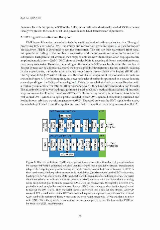
Appl. Sci. 2017, 7, 999
these results with the optimum SNR of the ASE spectrum-sliced and externally seeded RSOA schemes.Finally we present the results of bit- and power-loaded DMT transmission experiments.
2. DMT Signal Generation and Reception
DMT is a multi-carrier transmission technique with real-valued orthogonal subcarriers. The signalprocessing flow charts for a DMT transmitter and receiver are given in Figure 2. A pseudorandombit sequence (PRBS) is generated to test the transmitter. The bits are then rearranged from serialinto parallel according to the number of subcarriers and the information content in the respectivesubcarriers. Each parallel bit stream is then mapped onto its individual constellation (e.g., quadratureamplitude modulation—QAM). DMT gives us the flexibility to encode a different modulation formatonto every subcarrier. Therefore, depending on the available SNR at each subcarrier the number ofbits per symbol can be adapted to achieve the highest possible throughput, a feature called bit-loading.In our experiments, the modulation schemes ranged from binary phase shift keying (BPSK with1 bit/symbol) to 64QAM with 6 bit/symbol. The constellation diagrams of the modulation formats areshown in Figure 3. After bit mapping, the power of each subcarrier is optimized in a power-loadingstage depending on the SNR profile, see Figure 2. This is done such that all subcarriers will end up witha relatively similar bit error ratio (BER) performance even if they have different modulation formats.The adaptive bit-and power-loading algorithm is based on Chow’s method discussed in [38]. In a nextstep, an inverse fast Fourier transform (IFFT) with Hermitian symmetry is performed to obtain thereal valued DMT symbols. A cyclic prefix is added to each DMT symbol before being serialized andloaded into an arbitrary waveform generator (AWG). The AWG converts the DMT signal to the analogdomain before it is fed to an RF amplifier and encoded to the optical domain by means of an RSOA.
Figure 2. Discrete multi-tone (DMT) signal generation and reception flowchart. A pseudorandombit sequence (PRBS) is generated, which is then rearranged into a parallel bit-stream. Subsequently,adaptive bit mapping and power-loading are implemented. Inverse fast Fourier transform (IFFT) isthen used to encode the quadrature amplitude modulation (QAM) symbols on the DMT subcarriers.Cyclic prefix (CP) is added on the DMT symbols before the signal is converted back to serial. The serialdata is loaded onto an arbitrary waveform generator (AWG) which converts the digital signal to analogusing an inbuilt digital to analog converter (DAC). On the receiver side the signal is detected by aphotodiode and sampled by a real-time oscilloscope (RTO).Next, timing synchronization is performedto recover the DMT clock. Then the serial signal is converted into a parallel data stream. After CPremoval, FFT is used to decode the DMT subcarriers. Frequency and phase equalization of the receivedQAM symbols is performed. Here, we measure the error vector magnitude (EVM) and signal-to-noiseratio (SNR). Then, the symbols on each subcarrier are demapped to recover the transmitted PRBS forbit error ratio (BER) measurements.
57

Appl. Sci. 2017, 7, 999
Figure 3. Constellation diagrams of modulation formats used for the bit- and power-loaded DMTsignal generation. Binary phase shift keying (BPSK) encodes 1 bit/symbol. Quadrature phase shiftkeying (QPSK) encodes 2 bit/symbol. The quadrature amplitude modulation (QAM) formats: 8QAM,16QAM, 32QAM, and 64QAM encode 3, 4, 5 and 6 bit/symbol, respectively.
In the receiver, a direct detection scheme is used to detect the optical signals. The electricalsignals are then fed into a real-time oscilloscope (RTO). The RTO effectively digitizes the signal with aresolution of ~5.8 bits. In a first step, timing synchronization is performed using the non-data aidedDMT timing estimation technique discussed in [39]. Subsequently, the signal is parallelized and thecyclic prefix is removed.The subcarriers within the electrical signal are then derived by the fast Fouriertransform (FFT). To properly decode the bits within a subcarrier, blind phase and frequency offsetestimation methods are applied on every subcarrier [40]. The error vector magnitude (EVM) of theQAM symbols on each subcarrier is calculated and converted into SNR [41]. Then, the QAM symbolsare de-mapped to extract the received bit pattern. The BER is measured by comparing the transmittedand received bit patterns on each subcarrier. The overall BER is also measured by comparing the totaltransmitted and received bits.
3. Experimental Setups
In our experiments, we investigated the three colorless US transmitters in WDM-PON scenarios,see Figure 4. For all experiments, the transmitted DMT signal is generated offline with MATLAB andconverted to an analog waveform by an AWG (Keysight M8195A—60 GSa/s, Santa Rosa, CA, USA).The analog signal is amplified and a DC bias current is added before being fed to an RSOA. In all cases,a 1 mm long InGaAsP quantum well C-band RSOA (provided by III-V labs, 10G-RSOA-11-S, Palaiseau,France) is placed at the ONU. The distribution fiber (DF) links the ONU to the RN. At the RN, a flattop optical band-pass filter (OBPF) emulates the WDM filter. RN and CO are connected by the feederfiber (FF).
The three implementations of the RSOA based transmission links are shown in Figure 4 anddescribed in more detailed now.
Figure 4a shows the setup for the ASE spectrum-sliced scheme. In this scheme, the currentof an ROSA in the ONU is modulated with the data. This encodes the information onto the ASEoutput power of the RSOA. At the remote note, an OBPF (tuned to the emission center of the RSOA,which is at 1537.92 nm) band limits the modulated ASE-signal to the assigned wavelength channel.The filtered signal is then sent to the CO. The filter bandwidth has been chosen to be identical to thefilter bandwidth of the other schemes.
Figure 4b shows the setup for the self-seeded RSOA-FCL. Here, a Faraday rotator (FR) is placed atONU after the RSOA. In addition, a Faraday rotator mirror (FRM) is placed at the RN after a couplerbehind the WDM filter. The FRM and the RSOA reflective facet form the Fabry-Perot resonator cavityembedded in the DF. In case of RSOA with high polarization dependent gain (HPDG), the FR andFRM cancel out the birefringence effect in the cavity and maintain a constant polarization at the RSOAinput [42]. The coupler at the RN has a coupling ratio of 90/10, where 90% of the power is kept in thecavity and 10% is transmitted to the CO. The large amount of the power kept in the cavity is requiredto overcome cavity losses and thereby to achieve a net gain and with this lasing. In addition, the highpower in the cavity maintains the RSOA in the nonlinear operation region for better noise and residualmodulation suppression [17,43].
58

Appl. Sci. 2017, 7, 999
Figure 4c shows the experimental setup for the externally seeded RSOA scheme. Here, a lasersource (emitting at 1537.92 nm, similar to the other setups) at the CO seeds the RSOA at the ONUthrough the fiber link. The seeding power entering the RSOA has been optimized for the highest SNR.The RSOA now only serves as a modulator and amplifier for the respective laser wavelength.
Figure 4. Experimental setups of three RSOA based colorless transmitter schemes in a WDM-PONscenario: (a) ASE spectrum-sliced, (b) self-seeded RSOA-FCL, and (c) externally seeded RSOA. At theoptical network units (ONUs), the upstream signal from the arbitrary waveform generator (AWG) isamplified and added to a bias current to drive the RSOA. The ONU and the remote node (RN) areconnected by the distribution fiber (DF). At the RN, an optical bandpass filter (OBPF) mimics the WDMfilter. In the case of the RSOA-FCL in (b), the Faraday rotator mirror (FRM) is placed behind the filterand a coupler to form the Fabrey-Perot cavity, shown by the red dashed line. For the externally-seededRSOA in (c), the seeding cw laser is place at the central office (CO). On the receiver side at the CO,pre-amplification and direct detection are performed. A real-time oscilloscope (RTO) records theelectrical signal after the photodiode. An optical spectrum analyzer (OSA) is used to monitor theoptical signal at the CO. EDFA: Erbium doped fiber amplifier, VOA: variable optical attenuator.
In the three schemes, we implement only a single optical channel measurement due to lack ofequipment, however more than 16 channels have been demonstrated [2,21]. In all cases, the linkbudget between the ONU and the CO is ~12 dB (i.e., combination of all insertion losses of componentsin the link between ONU and CO). At the CO, a direct detection receiver detects the signals from thethree transmitters. Here, a 90/10 coupler sends 10% of the power to an optical spectrum analyzer(OSA) to monitor the signal. A variable optical attenuator (VOA) is used to control the power enteringthe preamplifier Erbium doped fiber amplifier (EDFA). A pre-amplified direct detection receiver isused here to guarantee that the signal quality measured here is as much as possible independent ofthe receiver scheme. A 5 nm flat top OBPF suppresses the out of band ASE noise from the EDFA.The optical signal is finally detected by a photodiode (PIN, responsivity 0.6 A/W), which is directlyconnected to a RTO (DSOX96204Q—20 GHz bandwidth and 40 GSa/s). The oscilloscope records thesignal for offline post-processing with MATLAB as outlined in Figure 2.
4. SNR Characterization
In this section, we present the measured SNRs versus subcarrier frequency offered by the threetransmitter schemes. Before presenting the results, we study the performance of the RSOA itself by
59

Appl. Sci. 2017, 7, 999
measuring the electrical modulation bandwidth. In a second step, we then focus on the self-seededRSOA-FCL. We study the impact of the WDM filter bandwidth in the RN, the fiber cavity lengthand the bias current on the SNR offered by the RSOA-FCL. Once the optimum operation parametersand limitations of the RSOA-FCL have been understood, we adjust the operation points of the ASEspectrum-sliced and the externally seeded RSOA. So for instance we set the WDM filter bandwidth ofthe ASE spectrum-sliced source to be identical with the RSOA-FCL. The input power for the externallyseeded transmitters is also set for maximum performance. Here we only give the operation points thathave been selected while one can find more details on finding the ideal operation points of an ASEspectrum-sliced transmitter in [44,45] and the externally seeded transmitter [25,46].
4.1. Electrical Bandwidth of the RSOA
We start our investigation by measuring the small signal modulation frequency response of theRSOA itself. We chose the externally seeded configuration to exclude the impact of dispersion and theexternal cavity. The frequency response for 50–120 mA bias current and at an input power of −3 dBmare plotted in Figure 5, which shows that the modulation response improves with higher bias current.At 100 mA, the RSOA exhibits −3 and −6 dB bandwidths of 2.4 and 4.55 GHz, respectively.
Figure 5. Measured small signal modulation frequency response of an RSOA at 50–120 mA biascurrents. The modulation bandwidth increases with bias current. At 100 mA, the RSOA has −3 and−6 dB bandwidths of 2.4 and 4.55 GHz.
4.2. RSOA-FCL Performance
Here, we perform three studies to analyze the performance of the RSOA-FCL: First, we investigatethe impact of the filter bandwidth in the cavity. Second, we study the SNR dependence on cavitylength and bias current. Last, we explore the transmission performance for different cavity lengthsat optimized operation conditions. In all cases, we use the SNR over the modulation frequency as ameasure for the link performance and for comparing parameters.
The SNR over the modulation frequency is measured according to the following procedure.We transmit DMT signals and evaluate the SNR on each subcarrier at the receiver. Here, the modulationformat and power of each subcarrier is identical. We generate a DMT signal having 256 subcarrierswith QPSK as modulation format and equal electrical power for all subcarriers. A PRBS 11 is used asthe transmitted bit sequence. The total symbol rate is 10 GBd. The IFFT size is 512 and a 2.5% cyclicprefix is added to each DMT symbol.
The signal is generated offline with MATLAB. An AWG generates the analog signal with 0.5 Vpp(peak-to-peak voltage). The output of the RF amplifier was optimized to ~3.5 Vpp. A bias tee combinesthe amplified signal with the specific bias current to drive the RSOA. On the receiver side, an RTOrecords the signal detected by a photodetector. Subsequently, the signal is demodulated in an offline
60

Appl. Sci. 2017, 7, 999
digital signal processing step. The measured EVM of the subcarriers is used to calculate the SNR ofeach subcarrier. This way, we can determine the frequency resolved SNR of the transmission linkacross the whole modulation bandwidth. This allows us to determine the usable bandwidth of thetransmission link. The useable bandwidth is the frequency band, within which the SNR is high enoughto still allow for a BER below 10−3 with BPSK modulation. Theoretically, a minimum SNR of 6.7 dBis required.
First, we investigated the impact of the WDM filter bandwidth in the RN. We compared OBPFbandwidths of 0.6 nm and 2 nm for three cavity lengths of 15 m, 115 m and 1 km standard singlemode fiber (SSMF). The bias current was maintained at 100 mA. Figure 6 shows the SNR over themodulation frequency for both cases. The SNR is higher for the filter with wider bandwidth for allcavity lengths. For a 0.6 nm filter, the 15 and 115 m cavities have a peak SNRs of ~14 dB. The maximumSNR obtained for the 1 km cavity with 0.6 nm is only ~12 dB. The usable bandwidth of the 15, 115 mand 1 km cavities with 0.6 nm filter was ~4.6, 4.5 and 2.7 GHz. When a 2 nm filter has been used in thereceiver one finds SNRs that are 5 dB higher. The usable bandwidth then increases by ~40% to ~6.7,~6.4 and ~4.5 GHz. The results are summarized in Table 1.
Figure 6. Measured SNR comparison of self-seeded RSOA-FCL transmitter with WDM filterbandwidths of 0.6 and 2 nm in RN. The dotted and solid lines show the measured SNR for the0.6 and 2 nm filters, respectively. For both cases, three different cavity lengths, 15 m, 115 m and 1 kmwere used. 0.6 nm filter cavity has peak SNR which is ~5 dB lower than that of the 2 nm one.
Table 1. Summary of results to compare the peak signal-to-noise ratio (SNR) and usable SNR bandwidthfor the RSOA-FCL (reflective semiconductor optical amplifier fiber cavity laser) with 0.6 nm or 2 nmfilter bandwidths. For both filters, the fiber cavity length varied between 15 m, 115 m and 1 km. OBPF:optical band-pass filter.
RSOA-FCL Cavity Length OBPF −3 dB Bandwidth Peak SNR (dB) Usable SNR Bandwidth (GHz)
15 m0.6 nm 14.3 4.62 nm 19.45 6.7
115 m0.6 nm 14.1 4.52 nm 19.5 6.4
1 km0.6 nm 11.9 2.72 nm 17.7 4.5
One explanation for the SNR degradation with narrower filters would be that a narrower filterleads to higher losses [47]. For example, at 100 mA, the reflected power into the RSOA was ~−6 dBmand ~−2 dBm for the 0.6 and 2 nm filters, respectively. Thus, higher losses means that the RSOA isless saturated. Therefore, the RSOA will be unable to efficiently suppress the residual modulation andnoise. As a consequence the RIN will be higher and the SNR is degraded [47]. The second explanationbased on [48] is that in case of highly multimode sources, increasing the number of modes (in this case
61

Appl. Sci. 2017, 7, 999
wider filter) will distribute the noise over the multiple modes thus lowering the noise spectral densityand RIN. Subsequently, we continue the investigation with the 2 nm filter only.
Next, we further investigated the impact of the distribution fiber cavity length and the biascurrent on the SNR of the self-seeded RSOA-FCL. We considered cavity lengths with 15 m, 115 mand 1 km SSMF to mimic WDM-PONs with distribution fibers in the range of tens of meters up to afew kilometers, for example in FTTA [49]. The RSOA bias current was set at 80, 100, 110 and 120 mA.Figure 7a,b show similar performance for cavities with 15 m and 115 m length. The insets in Figure 7a,bwhich are the transmitted (black curve) and the received (red curve) DMT electrical spectrums alsoshow similar characteristics. The similar performance originates from negligible chromatic dispersionfor the two lengths. In both cases, the frequency dependent SNR increases with the bias current, whichis related to the improved RSOA frequency response for higher bias currents as shown in Figure 5. TheSNR degradation for higher modulation frequencies is due to the bandwidth limitations of the RSOAas discussed in Figure 5. At 110 mA, both achieve maximum SNR of ~19 dB. The usable bandwidthwhere the SNR is still sufficiently high to receive a BPSK signal is ~6.7 and ~6.4 GHz for cavity lengthsof 15 m and 115 m, respectively.
Figure 7. Measured SNR versus subcarrier frequency of self-seeded RSOA-FCLs operated at 80, 100,110 and 120 mA bias currents for cavity lengths of (a) 15 m, (b) 115 m and (c) 1 km. The plots indicatethat the SNR bandwidth generally increases with the bias current. The 1 km cavity shown in (c) has areduced SNR peak and bandwidth when compared to the shorter cavities. The dashed line indicatesthe minimum SNR of 6.7 dB required to transmit BPSK, thus, it determines the usable bandwidth.In each plot, the insets show a sample electrical domain DMT spectra. The black and the red curvesshow the transmitted and received DMT electrical spectrum, respectively, at 110 mA. The receivedDMT spectrum for the 1 km cavity RSOA-FCL shown in plot (c) inset has a higher noise level comparedto that of the 15 and 115 m cavities spectra shown in insets of (a,b).
In Figure 7c we have plotted the SNR for the longer 1 km SSMF cavity. It is way lower than thosein Figure 7a,b. This can be understood by the fact that total accumulated chromatic dispersion is larger.Since the RSOA-FCL is highly multi-mode, chromatic dispersion leads to considerable mode partitionnoise. This noise increases the RIN [50,51], causing a SNR degradation. A bit higher loss of the 1 kmfiber cavity makes only a minor contribution to the SNR increase. At 110 mA, the maximum SNR is~17 dB only and the usable bandwidth is now ~4.5 GHz. In contrast to the RSOA-FCL with shortercavity lengths, the SNR in the 1 km cavity is not increasing with bias current. We expect that this
62

Appl. Sci. 2017, 7, 999
originates from the strong chirp during direct modulation at higher bias currents. The chirp causesspectral broadening which increases chromatic dispersion penalty. This induces an additional SNRdegradation for higher bias currents [52]. This is supported by the large noise level in the receivedelectrical DMT spectrum of the 1 km RSOA-FCL that can be seen in the inset of Figure 7c (red curve).However, the negative impact of the dispersive cavity on the SNR can be avoided by using O-bandRSOAs. In the O-band where chromatic dispersion is minimum, RSOA-FCL cavity could be extendedbeyond 1 km [22,53].
Finally, we investigated the SNR after transmission over 25 km NZDSF (chromatic dispersion:~5 ps/nm·km). This fiber is used to emulate a low dispersion PON fiber—similar to what one mightexpect if the system were operated in the O-Band. The probed SNR for the three cavity lengths for botha BtB and a 25 km transmission are plotted in Figure 8. When comparing the BtB and 25 km SNRs, themaximum SNR values for the respective cavity lengths did not show major change. Rather, the usableSNR bandwidth was reduced to ~3.3, 3.2 and 2.8 GHz for the 15 m, 115 m and 1 km cavities, respectively.The results are summarized in Table 2. This shows a 40–50% bandwidth reduction compared to the BtBcase. The finite signal bandwidth of the directly modulated RSOA results in chirp after propagationthat induces power fading and bandwidth reduction. In addition, such highly multi-mode sourcesuffers from mode partition noise induced by the NZDSF dispersion which increases the RIN.
Figure 8. Measured SNR to compare the impact of transmission fiber on the performance of anRSOA-FCL: The solid and dotted lines show the measured SNR for BtB (back-to-back) and after 25 kmnon-zero dispersion shifted fiber (NZDSF) transmission, respectively. In both cases, the results are for15 m, 115 m and 1 km fiber cavity lengths. The figure shows that the SNR bandwidth narrows by up to50% after transmission over 25 km fiber.
Table 2. Summary of results for the SNR performance of the RSOA-FCL with 15 m, 115 m and 1 kmcavities for back-to-back (BtB) and 25 km non-zero dispersion shifted fiber (NZDSF) transmission.
RSOA-FCL Cavity Length Tx Peak SNR (dB) Usable SNR Bandwidth (GHz)
15 mBtB 19.45 6.7
25 km NZDSF 19.01 3.2
115 mBtB 19.5 6.4
25 km NZDSF 19.2 3.2
1 kmBtB 17.7 4.5
25 km NZDSF 17.1 2.8
4.3. Performance Comparison of the Three Transmitter Schemes
Here, we compared the SNR performance of the ASE spectrum-sliced with the self-seededRSOA-FCL and the externally seeded RSOA sources. For this experiment, the ASE spectrum-slicedsource was equipped with the 2 nm filter, similar to that of the RSOA-FCL. For the RSOA-FCL, we tookthe 15 m and 1 km cavities, which offered the best and the worst performance, respectively. Both
63

Appl. Sci. 2017, 7, 999
RSOA-FCLs were equipped with a 2 nm filter. The RSOA input and output power for the externallyseeded scheme was −3 dBm, and ~6 dBm, respectively. The bias current for all experiments was setto 100 mA. Figure 9a,b show the measured SNR values for BtB and transmission over 25 km NZDSF,respectively. It can be seen that the externally seeded RSOA and the self-seeded RSOA roughly offer a10 dB and a 5 dB higher SNR over the ASE spectrum-sliced source across the whole spectral band. Theself-seeded RSOA-FCL with the shorter cavity outperforms the longer cavity FCL by about 1–2 dBacross the spectral band. And while the externally seeded RSOA exhibited the highest SNR bandwidthof ~9.6 GHz for BtB, the 15 m and 1 km long RSOA-FCLs offer useable bandwidths of 6.7 and 4.5 GHzand the ASE spectrum-sliced scheme features a usable bandwidth of only 2.5 GHz.
Figure 9. Comparison of the measured SNR for the three colorless transmitter schemes: RSOAASE spectrum-sliced (SS), self-seeded RSOA-FCL and externally seeded (ES) RSOA. (a) Shows theBtB (back-to-back) SNR measurement. The externally seeded RSOA (green line) outperforms theRSOA-FCL (red and brown) and the ASE spectrum-sliced scheme (blue) by ~10 and ~5 dB SNR acrossthe whole frequency range, respectively; (b) Shows the SNR after 25 km NZDSF transmission. TheSNR bandwidth is reduced due to dispersion of the transmission fiber. In general, the RSOA-FCL offersperformance midway between an ASE spectrum sliced and an externally seeded RSOA.
When transmitting the signals over 25 km NZDSF fiber, the usable SNR bandwidth reduced to~1.6 GHz for the ASE spectrum-sliced source. The RSOA-FCL declines to a usable bandwidths of 3 and2.8 GHz for the 15 m and 1 km long cavities. And the externally seeded RSOA still offers a 6.7 GHzbandwidth with sufficient SNR for transmission. The source of the SNR degradation with transmissionis the interplay of the chirp (induced by the direct modulation of the RSOA) and the dispersion ofthe transmission fiber. The narrower usable bandwidth recorded after transmission will influence themaximum achievable bit rate.
We attribute the higher performance observed for the RSOA-FCL when compared to the ASEspectrum-sliced source to three main factors. First, the RSOA-FCL has a significantly narrowerspectrum, which significantly reduces the impact of chromatic dispersion [17,50]. Second, theRSOA-FCL has a larger output power. For example, at 100 mA, the RSOA-FCL has an output power of−3.4 dBm while the ASE spectrum sliced scheme emits −11.8 dBm. Third, the saturated RSOA in thecavity nonlinearly suppress the amplitude noise in the lasing cavity, which lowers the RIN. These threecontribute to the improve SNR of the RSOA-FCL compared to the ASE spectrum sliced source [17].
5. Bit- and Power-Loaded DMT for Highest Bit Rates
In this section, bit- and power-loaded DMT transmission is used to maximize the data throughputfor any of the three bandwidth limited sources. We proceed in two steps. We again first study theimpact of the cavity length on the RSOA-FCL and the achievable data throughput in more detail. Onlywhen we know the optimum operation conditions of the RSOA-FCL, we investigate and compare themaximum capacity of all three schemes.
64

Appl. Sci. 2017, 7, 999
5.1. Maximizing the Capacity of the RSOA-FCL
In our experiments, we performed bit- and power-loading based on Chows algorithm [38]. Chow’salgorithm can briefly be described as follows. It takes in the SNR characterization of a transmitterat the subcarrier frequencies of the DMT signal. It also uses the SNR requirement of all advancedmodulation formats (see Figure 3) to achieve a predetermined BER. Then, it disregards subcarrierswith the lowest SNR that cannot support transmission at the predetermined BER for even the simplestformat. The power of such unusable subcarriers is then transferred to usable subcarriers. For subcarrierwith non-integer bit per symbol, the bit number is rounded off to the nearest integer, which requiresthe power to be re-adapted accordingly. This power adaptation step (power-loading) helps to achievesimilar BER for all subcarriers.
First, we performed bit- and power-loaded DMT transmission for the RSOA-FCL with 15 m,115 m and 1 km cavities. The signal was optimized for a BtB experiment and for transmission over25 km NZDSF. Figure 10a–c show the SNR, and the bit- as well as the power-loading patterns of theDMT and the measured per-subcarrier BER for 15 m, 115 m and 1 km long RSOA-FCLs, respectively.The 15 and 115 m cavities can support up to 5 bit/symbol (32QAM) for low frequency subcarriers.In case of the 1 km RSOA-FCL, the highest order modulation format is 16QAM, with 4 bits/symbol.The power-loading pattern is arranged to guarantee a minimum SNR difference for all subcarrierswith the same modulation format, so that a similar BER performance can be obtained. The solid linesin the BER plots indicate the overall BER, i.e., the total BER across all subcarriers. It can be seen thatthe overall BER is below 9.29 × 10⁻³ in all instances, which is the limit for an FEC (forward errorcorrection) with 12.5% overhead [54].
Figure 10. Measured SNR, bit- and power-loading pattern, and bit error ratio (BER) versus sub-carrierfrequencies and the achieved total line rate for different RSOA-FCL cavity lengths: Plots (a–c) showthe results for 15, 115 m and 1 km long cavities, respectively. The red and orange colors indicate BtB(back-to-back) and 25 km NZDSF transmission measurements. In all cases, the overall BER (solid linesin the BER plots) are kept below the FEC limit of 9.29 × 10⁻³ [53]; (d) Plots the measured total line ratefor 15, 115 m and 1 km long cavities, both for BtB and after 25 km transmission. In a BtB measurement,the RSOA-FCL offers up to 20 Gbit/s line rates. The line-rate is still 10 Gbit/s when transmittingsignals over 25 km.
65
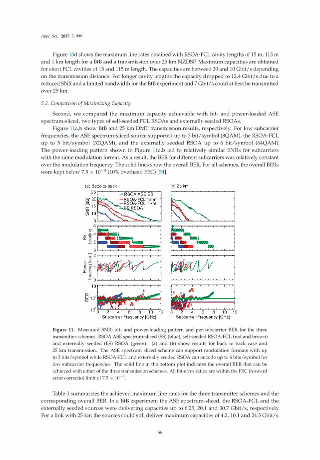
Appl. Sci. 2017, 7, 999
Figure 10d shows the maximum line rates obtained with RSOA-FCL cavity lengths of 15 m, 115 mand 1 km length for a BtB and a transmission over 25 km NZDSF. Maximum capacities are obtainedfor short FCL cavities of 15 and 115 m length. The capacities are between 20 and 10 Gbit/s dependingon the transmission distance. For longer cavity lengths the capacity dropped to 12.4 Gbit/s due to areduced SNR and a limited bandwidth for the BtB experiment and 7 Gbit/s could at best be transmittedover 25 km.
5.2. Comparison of Maximizing Capacity
Second, we compared the maximum capacity achievable with bit- and power-loaded ASEspectrum-sliced, two types of self-seeded FCL RSOAs and externally seeded RSOAs.
Figure 11a,b show BtB and 25 km DMT transmission results, respectively. For low subcarrierfrequencies, the ASE spectrum-sliced source supported up to 3 bit/symbol (8QAM), the RSOA-FCLup to 5 bit/symbol (32QAM), and the externally seeded RSOA up to 6 bit/symbol (64QAM).The power-loading pattern shown in Figure 11a,b led to relatively similar SNRs for subcarrierswith the same modulation format. As a result, the BER for different subcarriers was relatively constantover the modulation frequency. The solid lines show the overall BER. For all schemes, the overall BERswere kept below 7.5 × 10⁻³ (10% overhead FEC) [54].
Figure 11. Measured SNR, bit- and power-loading pattern and per-subcarrier BER for the threetransmitter schemes: RSOA ASE spectrum-sliced (SS) (blue), self-seeded RSOA-FCL (red and brown)and externally seeded (ES) RSOA (green). (a) and (b) show results for back to back case and25 km transmission. The ASE spectrum sliced scheme can support modulation formats with upto 3 bits/symbol while RSOA-FCL and externally seeded RSOA can encode up to 6 bits/symbol forlow subcarrier frequencies. The solid line in the bottom plot indicates the overall BER that can beachieved with either of the three transmission schemes. All bit-error ratios are within the FEC (forwarderror correctio) limit of 7.5 × 10⁻³.
Table 3 summarizes the achieved maximum line rates for the three transmitter schemes and thecorresponding overall BER. In a BtB experiment the ASE spectrum-sliced, the RSOA-FCL and theexternally seeded sources were delivering capacities up to 6.25, 20.1 and 30.7 Gbit/s, respectively.For a link with 25 km the sources could still deliver maximum capacities of 4.2, 10.1 and 24.5 Gbit/s.
66

Appl. Sci. 2017, 7, 999
It is interesting to note that the chirp-dispersion induced usable bandwidth reduction results inconsiderable capacity reduction, especially in the case of the ASE spectrum-sliced and RSOA-FCLtransmitters. This can be explained by the relatively wider linewidth of the two sources, thus incurringhigher dispersion penalty. However, O-band RSOAs [53], can be used to lower dispersion penalty andavoid the need for NZDSF. O-band has already been used for upstream transmission in legacy PONsto relax the requirement on inexpensive poor sources [1,55].
Table 3. Summary of achieved line rate and the respective bit error ratio (BER) for the three transmitterschemes. The results are for a BtB (back-to-back) and after 25 km NZDSF transmission. ASE: amplifiedspontaneous emitters.
ASE Spectrum-Sliced RSOA-FCL (15 m) RSOA-FCL (1 km) Externally Seeded RSOA
Line Rate(Gbit/s)
BERLine Rate(Gbit/s)
BERLine Rate(Gbit/s)
BERLine Rate(Gbit/s)
BER
BtB 6.25 5.8 × 10⁻³ 20.1 5.8 × 10⁻³ 12.4 5.8 × 10⁻³ 30.7 5.7 × 10⁻³
25 km NZDSF 4.2 2.3 × 10⁻³ 10.1 4 × 10⁻³ 7 5.8 × 10⁻³ 24.5 7.1 × 10⁻³
6. Conclusions
We show how transmission capacities of low-cost low-quality sources can be optimized formaximum capacities by means of bit- and power-loaded DMT transmission. Record high transmissiondata rates for an ASE spectrum-sliced, self-seeded RSOA-FCL and externally seeded RSOA of 6.25,20 and 30.7 Gbit/s in BtB and 4.2, 12.4 and 24.5 Gbit/s over 25 km NZDSF transmission are reported.To the best of our knowledge, these are the highest capacities reported for such inexpensive andcolorless sources. Our experiments show that even lowest cost sources such as spectral sliced ASEsources or RSOA-FCLs can offer quite some capacity if properly operated, for example, for O-bandupstream transmission. More precisely, ASE sources can provide capacities in the range of 6 to 4 Gbit/sdepending on the distance. Fabry-Perot sources such as the RSOA-FCL may offer capacities in theorder of 20 to 10 Gbit/s for distances up to 25 km. Finally, more costly externally seeded colorlesssources may provide capacities in the range of 30 to 25 Gbit/s if operated with an optimized bit- andpower loaded DMT transmission format without offset filtering.
Acknowledgments: This work was supported by the EU FP7 projects ERMES (grant agreement no. 288542) andFox-C (grant agreement No. 318415). Sterlite Technologies Ltd. is acknowledged for providing the fiber.
Author Contributions: Simon Arega Gebrewold conceived the concept, designed and performed the experiments,carried out the signal processing and analysis and wrote the paper. Romain Bonjour contributed in theconcept development, experiment and manuscript writing. Romain Brenot designed and fabricated the RSOAs.David Hillerkuss organized the experiment and wrote the paper. Juerg Leuthold conceived and developed theconcept, designed the experiment, wrote the paper and supervised the work.
Conflicts of Interest: The authors declare no conflict of interest.
References
1. Effenberger, F.J.; Mukai, H.; Park, S.; Pfeiffer, T. Next-generation PON-part II: Candidate systems fornext-generation PON. IEEE Commun. Mag. 2009, 47, 50–57. [CrossRef]
2. Vetter, P. Next generation optical access technologies. In Proceedings of the European Conference andExhibition on Optical Communication, Amsterdam, The Netherlands, 16–20 September 2012; Tu.3.G.1.
3. Pfeiffer, T. Next Generation Mobile Fronthaul and Midhaul Architectures [Invited]. J. Opt. Commun. Netw.2015, 7, 38–45. [CrossRef]
4. Saliou, F.; Gael, S.; Chanclou, P.; Pizzinat, A.; Lin, H.; Zhou, E.; Xu, Z. WDM PONs Based on ColorlessTechnology. Opt. Fiber Technol. 2015, 26, 126–134. [CrossRef]
5. Woodward, S.L.; Iannone, P.P.; Reichmann, K.C.; Frigo, N.J. A spectrally Sliced PON Employing Fabry-Perotlasers. IEEE Photonics Technol. Lett. 1998, 10, 1337–1339. [CrossRef]
6. Frigo, N.J. Recent Progress in Optical Access Networks. In Proceedings of the Optical Fiber Communications,San Jose, CA, USA, 25 February–1 March 1996; pp. 142–143.
67

Appl. Sci. 2017, 7, 999
7. Payoux, F.; Chanclou, P.; Genay, N. WDM-PON with Colorless ONUs. In Proceedings of the Optical FiberCommunication Conference and Exposition and the National Fiber Optic Engineers Conference, Anaheim,CA, USA, 25 March 2007.
8. Horiuchi, Y. Economical Solutions of the WDM-PON System. In Proceedings of the Optical FiberCommunication Conference, Los Angeles, CA, USA, 4–8 March 2012; pp. 1–3.
9. Healey, P.; Townsend, P.; Ford, C.; Johnston, L.; Townley, P.; Lealman, I.; Rivers, L.; Perrin, S.; Moore, R.Spectral Slicing WDM-PON Using Wavelength-Seeded Reflective SOAs. Electron. Lett. 2001, 37, 1181–1182.[CrossRef]
10. Han, K.H.; Son, E.S.; Choi, H.Y.; Lim, K.W.; Chung, Y.C. Bidirectional WDM PON using Light-EmittingDiodes Spectrum-Sliced with Cyclic Arrayed-Waveguide Grating. IEEE Photonics Technol. Lett. 2004, 16,2380–2382. [CrossRef]
11. Arellano, C.; Polo, V.; Bock, C.; Prat, J. Bidirectional Single Fiber Transmission Based on a RSOA ONU forFTTH Using FSK-IM Modulation Formats. In Proceedings of the Optical Fiber Communication Conference,Anaheim, CA, USA, 6–11 March 2005; JWA46.
12. Buset, J.M.; El-Sahn, Z.A.; Plant, D.V. Experimental Demonstration of a 10 Gb/s RSOA-based 16-QAMSubcarrier Multiplexed WDM PON. Opt. Express 2014, 22, 1–8. [CrossRef] [PubMed]
13. Wei, J.L.; Hugues-Salas, E.; Giddings, R.P.; Jin, X.Q.; Zheng, X.; Mansoor, S.; Tang, J.M. Wavelength ReusedBidirectional Transmission of Adaptively Modulated Optical OFDM Signals in WDM-PONs IncorporatingSOA and RSOA Intensity Modulators. Opt. Express 2010, 18, 9791–9808. [CrossRef] [PubMed]
14. Presi, M.; Cossu, G.; Chiuchiarelli, A.; Bottoni, F.; Corsini, R.; Choudhury, P.; Giorgi, L.; Ciaramella, E.25 Gb/s Operation of 1-GHz Bandwidth R-SOA by using DMT and Optical Equalization. In Proceedingsof the Optical Fiber Communication Conference and Exposition and the National Fiber Optic EngineersConference, Anaheim, CA, USA, 17–21 March 2013; OW1A.7.
15. De Valicourt, G.; Maké, D.; Landreau, J.; Lamponi, M.; Duan, G.H.; Chanclou, P.; Brenot, R. High Gain (30 dB)and High Saturation Power (11 dBm) RSOA Devices as Colorless ONU Sources in Long-Reach HybridWDM/TDM-PON Architecture. IEEE Photonics Technol. Lett. 2010, 22, 191–193. [CrossRef]
16. Lin, G.R.; Liao, Y.S.; Chi, Y.C.; Kua, H.C.; Lin, G.C.; Wang, H.L.; Chen, Y.J. Long-Cavity Fabrey-PerotLaser Amplifier Transmitter with Enhanced Injection-Locking Bandwidth for WDM-PON Application.J. Lightwave Technol. 2010, 28, 2925–2932. [CrossRef]
17. Gebrewold, S.A.; Bonjour, R.; Barbet, S.; Maho, A.; Brenot, R.; Chanclou, P.; Brunero, M.; Marazzi, L.;Parolari, P.; Totovic, A.; et al. Self-Seeded RSOA-Fiber Cavity Lasers vs. ASE Spectrum-Sliced or ExternallySeeded Transmitters—A Comparative Study. Appl. Sci. 2015, 5, 1922–1941. [CrossRef]
18. Sung-Bum, P.; Dae Kwang, J.; Dong, J.S.; Hong, S.S.; Yun, I.K.; Jeong, S.L.; Yun, K.O.; Yun, J.O. ColorlessOperation of WDM-PON Employing Uncooled Spectrum-Sliced RSOA. IEEE Photonics Technol. Lett. 2007,19, 248–250.
19. Henning, L.F.; Monteiro, P.; Almeida, A.D.; Pohl, P. Comparison of LED and RSOA performance inWDM-PONs. In Proceedings of the 21st International Conference on Telecommunications, Lisbon, Portugal,4–7 May 2014; pp. 124–128.
20. Wong, E.; Lee, K.L.; Anderson, T.B. Directly Modulated Self-Seeding Reflective Semiconductor OpticalAmplifiers as Colorless Transmitters in Wavelength Division Multiplexed Passive Optical Networks.J. Lightwave Technol. 2007, 25, 67–74. [CrossRef]
21. Marazzi, L.; Parolari, P.; Brenot, R.; De Valicourt, G.; Martinelli, M. Network-embedded self-tuning cavity forWDM-PON transmitter. Opt. Express 2012, 20, 3781–3786. [CrossRef] [PubMed]
22. Maho, A.; Gael, S.; Barbet, S.; Francois, L.; Saliou, F.; Chanclou, P.; Parolari, P.; Marazzi, L.; Brunero, M.;Martinelli, M.; et al. Demystification of the Self-Seeded WDM Access. J. Lightwave Technol. 2015, 34, 776–782.[CrossRef]
23. Le, S.D.; Lebreton, A.; Saliou, F.; Deniel, Q.; Charbonier, B.; Chanclou, P. Up to 60 km BidirectionalTransmission of a 16 Channels × 10 Gb/s FDM-WDM PON Based on Self-Seeded Reflective SemiconductorOptical Amplifiers. In Proceedings of the Optical Fiber Communications Conference and Exhibition (OFC),San Francisco, CA, USA, 9–13 March 2014; Th3G.8.
24. Shim, H.; Kim, H.; Chung, Y.C. 20-Gb/s Operation of RSOA using Polar Return-to-Zero 4-PAM ModulationFormat and Direct Detection. In Proceedings of the Optical Fiber Communication Conference, Los Angeles,CA, USA, 22–26 March 2015; W1J.2.
68

Appl. Sci. 2017, 7, 999
25. Cossu, G.; Bottoni, F.; Corsini, R.; Presi, M.; Ciaramella, E. 40 Gb/s Single R-SOA Transmission by OpticalEqualization and Adaptive OFDM. IEEE Photonics Technol. Lett. 2013, 25, 2119–2122. [CrossRef]
26. De Valicourt, G.; Make, D.; Fortin, C.; Enard, A.; Van-Dijk, F.; Brenot, R. 10 Gbit/s Modulation of RSOAwithout any Electronic Processing. In Proceedings of the Optical Fiber Communication Conference/NationalFiber Optic Engineers Conference, Los Angeles, CA, USA, 6–10 March 2011; OThT2.
27. Cho, K.Y.; Takushima, Y.; Chung, Y.C. 10-Gb/s Operation of RSOA for WDM PON. IEEE PhotonicsTechnol. Lett. 2008, 20, 1533–1535. [CrossRef]
28. Hoon, K. 10-Gb/s Operation of RSOA Using a Delay Interferometer. IEEE Photonics Technol. Lett. 2010, 22,1379–1381.
29. Torrientes, D.; Chanclou, P.; Laurent, F.; Tsyier, S.; Chang, Y.F.; Charbonnier, B.; Raharimanitra, F. RSOA-Based10.3 Gbit/s WDM-PON with Pre-Amplification and Electronic Equalization. In Proceedings of the OpticalFiber Communication Conference, Los Angeles, CA, USA, 21–25 March 2010; JThA28.
30. Papagiannakis, I.; Omella, M.; Klonidis, D.; Birbas, A.N.; Kikidis, J.; Tomkos, I.; Prat, J. Investigation of10-Gb/s RSOA-Based Upstream Transmission in WDM-PONs Utilizing Optical Filtering and ElectronicEqualization. IEEE Photonics Technol. Lett. 2008, 20, 2168–2170. [CrossRef]
31. Cho, K.Y.; Chung, Y.C. 10-Gb/s Operation of RSOA for WDM PON Using Return-to-Zero ModulationFormat. In Proceedings of the Optical Fiber Communication Conference and Exposition (OFC/NFOEC),Los Angeles, CA, USA, 4–8 March 2012; OTh1F.2.
32. Hyun Kyu, S.; Hoon, K.; Yun, C.C. 20-Gb/s Polar RZ 4-PAM Transmission over 20-km SSMF Using RSOAand Direct Detection. IEEE Photonics Technol. Lett. 2015, 27, 1116–1119.
33. Zhang, Q.W.; Hugues-Salas, E.; Ling, Y.; Zhang, H.B.; Giddings, R.P.; Zhang, J.J.; Wang, M.; Tang, J.M.Record-high and robust 17.125 Gb/s gross-rateover 25 km SSMF transmissions of real-time dual-band opticalOFDM signals directly modulated by 1 GHz RSOAs. Opt. Express 2014, 22, 6339–6348. [CrossRef] [PubMed]
34. Xie, C.; Dong, P.; Randel, S.; Winzer, P.; Spiga, S.; Koegel, B.; Neumeyr, C.; Amann, M.C. Single-VCSEL100-Gb/s Short-Reach System Using Discrete Multi-Tone Modulation and Direct Detection. In Proceedingsof the Optical Fiber Communications Conference and Exhibition (OFC), Los Angeles, CA, USA, 22–26 March2015; pp. 1–3.
35. Takahara, T.; Tanaka, T.; Nishihara, M.; Kai, Y.; Li, L.; Tao, Z. Discrete Multi-Tone for 100 Gb/s OpticalAccess Networks. In Proceedings of the Optical Fiber Communication Conference, San Francisco, CA, USA,9–13 March 2014; M2l.1.
36. Nadal, L.; Moreolo, M.S.; Fabrega, J.M.; Dochhan, A.; Griesser, H.; Eiselt, M.; Elbers, J.P. DMT ModulationWith Adaptive Loading for High Bit Rate Transmission Over Directly Detected Optical Channels.J. Lightwave Technol. 2014, 32, 4143–4153. [CrossRef]
37. Gebrewold, S.A.; Brenot, R.; Bonjour, R.; Josten, A.; Baeuerle, B.; Hillerkuss, D.; Hafner, C.; Leuthold, J.Colorless Low-Cost RSOA Based Transmitters Optimized for Highest Capacity Through Bit- andPower-Loaded DMT. In Proceedings of the Optical Fiber Communication Conference, Anaheim, CA, USA,20–22 March 2016; Tu2C.4.
38. Chow, P.S.; Cioffi, J.M.; Bingham, J.A. A practical Discrete Multitone Transceiver Loading Algorithm forData Transmission over Spectrally Shaped Channels. IEEE Trans. Commun. 1995, 43, 773–775. [CrossRef]
39. Pollet, T.; Peeters, M. Synchronization with DMT modulation. IEEE Commun. Mag. 1999, 37, 80–86.[CrossRef]
40. Nakagawa, T.; Kobayashi, T.; Ishihara, K.; Miyamoto, Y. Non-Data-Aided Wide-Range Frequency OffsetEstimator for QAM Optical Coherent Receivers. In Proceedings of the Optical Fiber CommunicationConference/National Fiber Optic Engineers Conference, Los Angeles, CA, USA, 6–10 March 2011; OMJ1.
41. Schmogrow, R.; Nebendahl, B.; Winter, M.; Josten, A.; Hillerkuss, D.; Koenig, S.; Meyer, J.; Dreschmann, M.;Huebner, M.; Koos, C.; et al. EVM as a Performance Measure for Advanced Modulation Formats.IEEE Photonics Technol. Lett. 2012, 24, 61–63. [CrossRef]
42. Martinelli, M.; Marazzi, L.; Parolari, P.; Brunero, M.; Gavioli, G. Polarization in Retracing Circuits forWDM-PON. IEEE Photonics Technol. Lett. 2012, 24, 1191–1193. [CrossRef]
43. Marazzi, L.; Parolari, P.; Boletti, A.; Gatto, A.; Martinelli, M.; Brrnot, R. Highly-nonlinear RSOA RINcompression. In Proceedings of the 19th European Conference on Networks and Optical Communications,Milano, Italy, 4–6 June 2014; pp. 115–119.
69

Appl. Sci. 2017, 7, 999
44. Kani, J.; Kawata, H.; Iwatsuki, K.; Ohki, A.; Sugo, M. Design and Demonstration of Gigabit Spectrum-SlicedWDM Systems Employing Directly Modulated Super Luminescent Diodes. In Proceedings of the OpticalFiber Communication Conference and Exposition and the National Fiber Optic Engineers Conference,Anaheim, CA, USA, 6–11 March 2005; JWA49.
45. Pendock, G.J.; Sampson, D.D. Transmission performance of high bit rate spectrum-sliced WDM systems.J. Lightwave Technol. 1996, 14, 2141–2148. [CrossRef]
46. Wei, J.L.; Hamie, A.; Gidding, R.P.; Hugues-Salas, E.; Zheng, X.; Mansoor, S.; Tang, J.M. AdaptivelyModulated Optical OFDM Modems Utilizing RSOAs as Intensity Modulators in IMDD SMF TransmissionSystems. Opt. Express 2010, 18, 8556–8573. [CrossRef] [PubMed]
47. Marazzi, L.; Parolari, P.; Brunero, M.; Gatto, A.; Martinelli, M.; Brenot, R.; Barbet, S.; Galli, P.; Gavioli, G. Upto 10.7-Gb/s High-PDG RSOA-Based Colorless Transmitter for WDM Networks. IEEE Photonics Technol. Lett.2013, 25, 637–640. [CrossRef]
48. Petermann, K. Noise Characterstics of Solitary Laser Diodes. In Laser Diode Modulation and Noise; Okoshi, T.,Ed.; Kluwer Academic Publishers: Dordrecht, The Netherlands, 1998; pp. 152–208.
49. Ma, Y.; Xu, Z.; Lin, H.; Zhou, M.; Wang, H.; Zhang, C.; Yu, J. Demonstration of Digital Fronthaul OverSelf-Seeded WDM-PON in Commercial LTE Environment. Opt. Express 2015, 23, 11927–11935. [CrossRef][PubMed]
50. Gebrewold, S.A.; Marazzi, L.; Parolari, P.; Brenot, R.; Duill, P.O.S.; Bonjour, R.; Hillerkuss, D.; Hafner, C.;Leuthold, J. Reflective-SOA Fiber Cavity Laser as Directly Modulated WDM-PON Colorless Transmitter.IEEE J. Sel. Top. Quantum Electron. 2014, 20, 1–9. [CrossRef]
51. Gebrewold, S.A.; Marazzi, L.; Parolari, P.; Brunero, M.; Brenot, R.; Hillerkuss, D.; Hafner, C.; Leuthold, J.Colorless Self-Seeded Fiber Cavity Laser Transmitter for WDM-PON. In Proceedings of the CLEO: Scienceand Innovations, San Jose, CA, USA, 8–13 June 2014; STu1J.4.
52. André, N.S.; Habel, K.; Louchet, H.; Richter, A. Adaptive Nonlinear Volterra Equalizer for Mitigation ofChirp-Induced Distortions in Cost Effective IMDD OFDM Systems. Opt. Express 2013, 21, 26527–26532.[CrossRef] [PubMed]
53. Simon, G.; Saliou, F.; Chanclou, P.; Deniel, Q.; Erasme, D.; Brenot, R. 70 km external cavity DWDM sourcesbased on O-band Self Seeded RSOAs for transmissions at 2.5 Gbit/s. In Proceedings of the Optical FiberCommunication Conference, San Francisco, CA, USA, 9–13 March 2014; W3G.5.
54. Zhang, L.M.; Kschischang, F.R. Staircase Codes with 6% to 33% Overhead. J. Lightwave Technol. 2014, 32,1999–2002. [CrossRef]
55. Bonk, R.; Brenot, R.; Meuer, C.; Vallaitis, T.; Tussupov, A.; Rode, J.C.; Sygletos, S.; Vorreau, P.; Lelarge, F.;Duan, G.H.; et al. 1.3/1.5 μm QD-SOAs for WDM/TDM GPON with Extended Reach and LargeUpstream/Downstream Dynamic Range. In Proceedings of the Optical Fiber Communication—Incudespost deadline papers, San Diego, CA, USA, 22–26 March 2009; OWQ1.
© 2017 by the authors. Licensee MDPI, Basel, Switzerland. This article is an open accessarticle distributed under the terms and conditions of the Creative Commons Attribution(CC BY) license (http://creativecommons.org/licenses/by/4.0/).
70

applied sciences
Article
Theoretical Analysis of Directly Modulated ReflectiveSemiconductor Optical Amplifier PerformanceEnhancement by Microring Resonator-BasedNotch Filtering
Zoe V. Rizou * and Kyriakos E. Zoiros
Lightwave Communications Research Group, Laboratory of Telecommunications Systems,Department of Electrical and Computer Engineering, Democritus University of Thrace, 67 100 Xanthi,Greece; [email protected]* Correspondence: [email protected]; Tel.: +30-25410-79-975
Received: 30 December 2017; Accepted: 28 January 2018; Published: 1 February 2018
Abstract: We demonstrate the feasibility of using a single microring resonator (MRR) as optical notchfilter for enabling the direct modulation of a reflective semiconductor optical amplifier (RSOA) at morethan tripled data rate than possible with the RSOA alone. We conduct a thorough simulation analysisto investigate and assess the impact of critical operating parameters on defined performance metrics,and we specify how the former must be selected so that the latter can become acceptable. By usingan MRR of appropriate radius and detuning, the RSOA modulation bandwidth, which we explicitlyquantify, can be extended to overcome the RSOA pattern-dependent performance limitations. Thus,the MRR makes the RSOA-encoded signal exhibit improved characteristics that can be exploited inpractical RSOA direct modulation applications.
Keywords: direct modulation; microring resonator; optical notch filter; reflective semiconductoroptical amplifier
1. Introduction
Reflective semiconductor amplifiers (RSOAs) are key modules for the realization of next-generationbroadband access applications, such as colorless passive optical access networks [1], radio over fiber [2],slow and fast light [3], data erasing and remodulation [4], information packet power equalization [5] andfiber-optical cable television [6], which rely on the manipulation of data flowing in opposite directions.In effect, a single RSOA can simultaneously receive and amplify signals in the downstream whileremodulating them with end-user information in the upstream communication link. This multifunctionalcapability is inherent to RSOAs, which owing to their internal structure use the same device facet bothfor signal input injection and output extraction. Thus, RSOAs avoid the need of having extra fiber paths,fiber components and optoelectronic elements to support bidirectional transmission, which helps reducethe overall system cost and complexity. However, as a physical byproduct of semiconductor opticalamplifiers’ finite carrier lifetime [7], the modulation bandwidth, which scales inversely against thisparameter [8], of these devices, including RSOAs, is limited to a few GHz. For this reason, an RSOAcan be directly modulated by electrical data, which are encoded on a seeding continuous wave (CW)light, only up to speeds which are not sufficient for satisfying the increasing bandwidth needs of thetarget applications. In the effort to overcome this fundamental limitation towards enabling full-duplexand symmetrical RSOA-based data transfer, several promising options are available, which includeelectronic equalization [9], advanced modulation formats [10,11], specially designed RSOA packageand driving circuitry [12,13], and optical notch filtering [14]. In particular, the latter has been widelyexploited because of the simple configuration, cost-affordable implementation using off-the-shelf
Appl. Sci. 2018, 8, 223; doi:10.3390/app8020223 www.mdpi.com/journal/applsci71

Appl. Sci. 2018, 8, 223
components and passive nature of the underlying signal-equalization mechanism. Furthermore, it isnot concerned with challenging issues of the three other alternatives, such as the sensitivity to fiberchromatic dispersion and the requirement of high-speed sophisticated electronics at the transmitter andreceiver side, in the first; the inevitable complex signal generation and detection in the second; and theinvolvement of elaborate fabrication and integration processes in the third. In fact, the two first RSOAbandwidth-extension techniques have even been combined with optical equalization and benefitedfrom its efficiency to further improve their performance [11,15,16]. Thus, different schemes that act asoptical notch filters on RSOA-encoded outputs have been reported, such as the delay interferometer(DI) [17,18], the fiber Bragg grating (FBG) [19] and the arrayed waveguide grating (AWG) [20].In the same technological category also fall schemes that have been applied on conventional directlymodulated SOAs, such as the birefringent fiber loop (BFL), either alone [21], in cascade with anotherBFL [22] or assisted by an optical bandpass filter [23]; and the microring resonator (MRR) [24]. The MRRis a special form of powerful waveguides [25,26], and exhibits distinctive characteristics over theaforementioned types of employed filters. These include the structural simplicity, the ultra-compactsize–which makes it amenable to integration with microelectronic fabrication processes–enhancedwavelength selectivity, fine-tuning capability and availability of different material systems with thepotential of copackaging with the SOA in the same hybrid platform. These attributes render theMRR a mostly suitable solution for increasing the operating speed of directly modulated RSOAsas well. In this paper, we investigate and demonstrate, by means of theoretical simulation andanalysis, the MRR potential for overcoming the RSOA limited modulation bandwidth and thus forbeing extended beyond classical filter-oriented applications. For this purpose, we apply the modelproposed in [27] to theoretically describe the operation of an RSOA when directly modulated by anelectrical data pattern, a task that we initiated within the frame of [28]. Unlike the usually followedmodeling approach, which involves solving a set of coupled partial nonlinear differential equationswith boundary conditions [29,30], and hence is computationally demanding, this reduced model hasbeen formulated on the basis of valid assumptions and prior framework [31] in such way that it allowsone to derive the encoded signal at the RSOA output from the solution of a single standard differentialequation in the time domain. This fact greatly simplifies the computational complexity while stillproviding realistic and accurate results. In this manner, we have been able to explore the capabilityof the MRR to enhance the data rate at which the RSOA can be directly modulated with acceptableperformance. We have thus confirmed that if the MRR critical parameters are selected as specified inthis work, it is indeed possible to extend by more than three times the repetition rate of the encodedsignal, with the latter exhibiting improved characteristics.
2. RSOA Direct Modulation Assisted by MRR-Based Notch Filtering
2.1. Configuration
The basic configuration of a directly modulated RSOA is shown in Figure 1. A CW signal of constantpower, PCW , is inserted in the RSOA. Concurrently, a radio frequency (RF) signal, which comprisesnon-return-to-zero (NRZ) data pulses, is superimposed to the RSOA DC bias current, Ibias, and induces,via the RSOA electrical impedance, a peak current offset, ±Im. Since the RSOA rear edge is highlyreflective, the CW signal undertakes a double pass inside the active medium of length L, and when itexits from the RSOA front facet, which is highly antireflective, it has perceived the gain variations dueto the modulated current. Normally, the CW signal at the RSOA output should bear the exact digitalinformation of the applied electrical excitation in optical form. However, as the rate of direct modulationgets faster, this may not happen, as due to the RSOA limited modulation bandwidth, the performance ofthe directly modulated RSOA is progressively deteriorated by pattern effects and eventually becomespoor. Still, it is possible to enhance the RSOA direct modulation capability by means of optical notchfiltering. For this purpose, the RSOA is connected to an MRR, which, as shown in Figure 1, is a waveguideshaped into a ring structure of radius R coupled to a bus waveguide with field transmission coefficient r.
72

Appl. Sci. 2018, 8, 223
By properly tailoring the MRR spectral response, the MRR can efficiently act as frequency discriminatoron the encoded pulses and improve their quality. This is done by adjusting the wavelength separationbetween adjacent peaks or notches, or free spectral range (FSR), which is inversely proportional to theMRR radius, and wavelength offset, that is, detuning, Δλ, between the encoded signal spectral position,λenc, and the nearest transfer function (TF) transmission peak, while maximizing the MRR transferfunction peak-to-notch contrast ratio (PNCR) through operating the MRR in the critical coupling regime,where the microring internal losses are equal to the coupling losses. In this manner, the MRR compensatesfor the inherently limited bandwidth of the RSOA, and mitigates the pattern-dependent impairmentsinduced on the encoded pulses.
Figure 1. Conceptual view of reflective semiconductor amplifier (RSOA) direct modulation assisted byserially connected microring resonator (MRR). FSR: free spectral range, RF: radio frequency.
2.2. Modeling
The performance of the setup in Figure 1 is characterized by the power that emerges at the outputof the directly modulated RSOA, PRSOA(t), and of the cascaded MRR-based notch filter, PMRR(t).This means that in order to simulate the operation of the scheme, it is necessary to know and calculateat each one of these points the lightwave-encoded signal electric fields, since they are normalized sothat their squared modulus represents power, that is, PRSOA,MRR(t) =
∣∣ERSOA,MRR(t)∣∣2 [32].
For the RSOA case
ERSOA(t) =√
PCW exp[(1 − jαLEF)h(t − 2Lng/c)
], (1)
where αLEF is the RSOA linewidth enhancement factor, ng is the group refractive index of thesemiconductor material, c is the speed of light in vacuum, and the RSOA gain response integratedover its length is denoted by h(t), which is shifted in time by twice the RSOA one-way transit timeso as to account for the double pass taken by the lightwave signal within the RSOA optical cavity.Now, function h(t) obeys the following one-dimensional differential equation [27]
dh(t)dt
= −h(t)− ΓaN0L
[I(t)I0
− 1
]Tcar
− exp[2h(t)
]− 1Esat
PCW , (2)
73

Appl. Sci. 2018, 8, 223
where Γ is the RSOA confinement factor, a is the RSOA differential gain, N0 is the RSOA carrierdensity at transparency, Tcar is the RSOA carrier lifetime, I0 = qALN0/Tcar is the RSOA current attransparency (where q is the electron charge and A is the area of the semiconductor active region),and Esat is the RSOA saturation energy. Equation (2) has been obtained after making the followingvalid assumptions and simplifications: (a) The RSOA internal losses are neglected, as they can bewell compensated by the RSOA CW gain, GCW , through the adjustment of the RSOA bias current,since these two parameters are directly related [27]; (b) the RSOA reflectivity is considered perfect,that is, 100%, as in practice this is a basic feature of the specific devices that favors their use [33],in particular as intensity modulators [10]; and (c) the RSOA round-trip propagation time, which isdetermined by the RSOA active region length, is smaller than the pulse repetition interval of theapplied excitation. This condition is satisfied for the direct modulation rates pursued in RSOAs beingless than 1 mm long [34].
The profile of each pulse inside the N = 27 − 1 bit-long NRZ pseudorandom binary sequence(PRBS) of the injection current is described in compact form [35,36] as the sum of a DC term anda modulation term
I(t) =
DC term︷ ︸︸ ︷(Ibias − Im) +
ΔI(t)≡ modulation term︷ ︸︸ ︷2Im
{H(t)[
1 − e−t2/t2r
]− H(t − T)
[1 − e−(t−T)2/t2
r
]}, (3)
where H(t) is Heaviside step function, Ibias and Im are the RSOA bias current and induced RFmodulation current, respectively–which are a small fraction of the current at transparency–and tr isthe pulse rise time, which occupies a small portion of the pulse repetition period, T.
For the MRR case, obtaining the electric field at its output involves the following steps. First,the RSOA temporal response is extracted by numerically solving for h(t) from (2). This is done byfollowing the numerical method formulated in [37] but adapted to account for a temporal-dependenttotal injection current [38]. More specifically, for each information bit of duration T carried by themodulation current, (2) is solved in a step-wise manner by approximating the time derivative of h(t)by a finite difference and applying the appropriate initial conditions. For this purpose, the continuoustime variable t is replaced by discrete points tp,i = (p − 1)T + iΔt, for p = 1, 2, . . . , N and i = 1, 2, . . . , k,where p denotes the p-th pulse inside the N-long PRBS of the injection current, Δt is the finite temporalincrement and k = T/Δt is the integer number of calculated samples of function h(t) in each bit period.To ensure high enough temporal resolution and at the same time enhanced computational efficiencyso as to correctly capture the RSOA gain dynamics expressed by h(t) with affordable hardware andsoftware resources, we choose Δt = 1 ps, which means that nearly 100 samples are taken at all datarates considered in this paper. Then, the knowledge of h(t) and of its derivative at a given pulse instant“i”, hp,i and dhp,i/dt, respectively, allows one to calculate the value, h(t + Δt), at the next discretemoment, hp,i+1, according to Euler’s numerical method. This method is suitable for studying theresponse of semiconductor active waveguide devices, such as the RSOA, to an electrical excitationof piecewise varying nature, such as the injection current NRZ pulses, as it converges rather fastwhile producing reasonable results [39]. The initial conditions required for running this process are(a) h1,1 = g0L, where g0 = ΓaN0
{[(Ibias − Im)/I0
] − 1}
is the RSOA steady-state gain coefficient.This condition is a direct byproduct of the fact that the first temporal segment in the leading edge ofthe very first information pulse, which is assumed to be a mark and is supplied to the RSOA throughthe injection current pulse stream, experiences an unsaturated RSOA gain, since the carriers of thelatter have not had the time to be modified yet; (b) hp,1 = hp−1,k, to account for the fact that the gainavailable to the first temporal segment in the leading edge of every next pulse is that left by the lasttemporal segment of the immediately preceding pulse. This condition is properly adapted and reducedto the case of consecutive NRZ pulses carrying the same binary information, that is, strings of marks orspaces. This process is carried out iteratively until all N · k-th values of h(t) are obtained, which can be
74

Appl. Sci. 2018, 8, 223
then stored in a matrix and retrieved for further calculations. The solution for h(t) is then substitutedin (1) to find the electric field of the encoded signal at the RSOA output. This function is transferredthen into the frequency domain and is convolved with the MRR spectral response. The latter has thecompact mathematical expression given below [40],
TMRR(λ) =r − l exp
[jne f f 4π2R
((λ − Δλ)/λ2)]
1 − rl exp[
jne f f 4π2R((λ − Δλ)/λ2
)] , (4)
where ne f f is the waveguide effective refractive index while the field transmission coefficient, r,and amplitude attenuation factor, l, are equal and tend to unity so as to ensure that the MRR isoperating in the critical coupling regime [41] where it can efficiently act as notch filter [42]. Then,the convolution product is converted back into the time domain. This procedure can be put inmathematical form as EMRR(t) = F−1{F [ESOA(t)
]TMRR(λ)}, where operators, F{·} and F−1{·}
denote fast Fourier transform (FFT) and inverse FFT, respectively, which are both available andexecuted in Matlab software. Therefore, PMRR(t) = |EMRR(t)|2. In this manner, the maximum andaverage values of the peak power of the marks and spaces within the encoded PRBS can be found sothat they can be used to calculate the performance metrics employed in the following section.
The operation of the directly modulated RSOA, either alone or assisted by the MRR, is alsocharacterized by the respective modulation responses, which are derived through the process ofsmall-signal analysis [43,44]. Starting with the RSOA, we have
TRSOA1©=
pRSOA(Ωm)
pRSOA(0)2©=
Δh(Ωm)
Δh(0)3©=
Δg(Ωm)D(0)Δg(0)D(Ωm)
, (5)
where the expressions that follow after steps 1©, 2© and 3© have been derived by combining relevantinformation from [18,27] and [45] (c.f. Appendix). More specifically, in 1©, pRSOA(Ωm) is thesmall-signal power, which is produced at the RSOA output due to the modulation of its currentat a given frequency, fm = Ωm/2π, and normalized over its unmodulated counterpart [46]; in 2©,Δh(Ωm) is the concomitant small-signal deviation from steady state of the RSOA-integrated gain givenby [27] Δh(Ωm) = [L/D(Ωm)]Δg(Ωm), where Δg(Ωm) = ΓaN0ΔI(Ωm)/I0 is the correspondinggain coefficient perturbation incurred by the modulation current of complex envelope ΔI(Ωm);
and in 3©, D(Ωm) = 1 − jΩmTcar + W
[2TcarPCW
Esatexp(
2g0L +2TcarPCW
Esat
)][27], where W[·] is
Lambert’s ‘W’ function [47]. Function D(Ωm) links in a compact manner the perturbation of theRSOA-integrated gain to the current modulation from which it has been incurred. Thus, when theRSOA is directly modulated by a sinusoidal electrical excitation, it allows, through first-orderapproximations, one to analytically express the 3 dB angular frequency of the RSOA modulation
response as [27] Ω3dB =
√3
Tcar
{1 + W
[2TcarPCW
Esatexp(
2g0L +2TcarPCW
Esat
)]}. This formula provides
an estimate of the maximum RSOA modulation frequency and hence of its direct modulation capabilityat a given data rate [28]. In general, however, the modulation current may be in digital form andhave any shape. Then, the 3-dB modulation bandwidth can be derived from (5) by taking the Fouriertransform of the modulation current in the time domain, which in our case is given by the secondterm in the right-hand side of (3). By using Fourier transform formulas and properties of the functionsinvolved therein, and after tight algebraic manipulations, in the course of which the complementaryerror function and the imaginary error function come into being, we find the explicit expression
ΔI(Ωm) = F [ΔI(t)] =
= 2Im
{1
jΩm
[1 − exp(−jΩmT)
]+[
exp(−jΩmT)− 1][
0.5√
πtr exp(− Ω2
mt2r /4)− jtrF(Ωmtr/2)
]},
(6)
75

Appl. Sci. 2018, 8, 223
where function F(x) = exp(−x2)x∫
0exp(t2)dt represents Dawson’s integral [48], which is available
in Matlab software. Taking the squared modulus and after proper algebraic manipulations, (6) canbe brought into a form that allows one to approximate its values for the boundary conditions ofthe modulation frequency [46]. The obtained result is analogous to the square of the product of theelectrical modulation pulses’ peak amplitudes and period when Ωm → 0, while it tends to null whenΩm → ∞. In other words, the level of the specific function in these two limits is in the oppositedirection to that of the modulation frequency variation. This fact confirms that the RSOA modulationresponse exhibits a low-pass characteristic, which is in agreement with the same trend noticed fromextensive numerical calculations [49].
For the MRR, on the other hand, the modulation response is [24]
TMRR = A × ((1 − jαLEF)/2)× A∗+Ω2
m+2δΩm+jμ2e Ωm
δ2((δ+Ωm)2+1/τ2
) +
+A∗ × ((1 + jαLEF)/2)× A+Ω2
m−2δΩm+jμ2e Ωm
δ2((δ−Ωm)2+1/τ2
) .(7)
In this expression, A = δ2 − jμ2e δ (and A∗ is the complex conjugate), δ = 2πc
λnotch − λenc
λnotchλenc,
where λnotch is the spectral position of the MRR transfer function notch (Figure 1) that obeys thecondition of MRR resonance, 2πRne f f = mλnotch, m ∈ Z∗, and lies nearest to the encoded opticalsignal of wavelength, λenc, in the vicinity of 1550 nm, and μe is the coupling strength between thebus waveguide and the ring, μ2
e =[(1 − r2)c/2πRne f f
]= 1/τ, where the last equality with the MRR
1/e amplitude decay time, τ, holds under critical coupling [44]. The modulation response of theMRR-assisted RSOA is then obtained by taking the absolute value of (5) and multiplying it with themodulus of (7).
Finally, an inevitable consequence of RSOA direct modulation is that the encoded pulses acquirean instantaneous frequency deviation, that is, chirp, across them [50]. The compensation of the chirp’sirregular temporal variation via post-optical notch filter is converted by the latter to restored quality ofencoded pulses and accordingly enhanced RSOA modulation capability. This means that quantifyingthis transient effect can also provide useful information for the operation and performance of theMRR-assisted directly modulated RSOA. For this purpose, the knowledge of the phase responseof the RSOA and MRR is required since the chirp, Δv(t), is by definition linked to it through thederivative in the time domain [51]. Finding the chirp for the SOA case is straightforward by isolatingthe output phase term from (1), differentiating it in time and readily taking the differential of thetime-delayed version of the RSOA-integrated gain response from the right-hand side of (2) using thetransform t → t − 2Lng/c. For the MRR case, however, the phase of the transmitted light undergoesa steep variation around resonance [52], which compromises the direct numerical calculation of thecorresponding response and accordingly of its temporal rate of change, which provides the chirp.Instead of taking the inverse tangent function of the ratio between the imaginary and real parts of thecomplex-valued electric field [53], we use the relevant information that is extracted when applyingthe signal phase-reconstruction technique in the optical domain [54,55]. This technique allows oneto unambiguously recover the instantaneous frequency deviation profile of a random repetitive datasignal which is inserted in a frequency discriminator whose spectral transfer function has a linearspectral amplitude variation around the detuning position. This element acts as a differentiator on theinserted signal, which is exactly what the MRR-based notch filter does in our case [52]. In this manner,the desired chirp can be directly extracted in analytical form from the knowledge of the time-domainintensity profiles of the signals that enter and exit the MRR. Thus [54],
−2πΔvMRR(t) = −√√√√ 1
|ERSOA(t)|2 ·[(
|EMRR(t)|S
)2
−(
∂|ERSOA(t)|∂t
)2]+ δ, (8)
76

Appl. Sci. 2018, 8, 223
where S is the slope of the linear amplitude variation around the detuning point of the MRR TF withrespect to angular frequency, which can be found by differentiating (4) and applying the chain rule [56].
3. Results
We found first if and how the RSOA can be directly modulated on its own without performancedegradation. For this purpose we investigated the impact of the parameters associated with the opticaland electrical RSOA excitation signal on the error probability (EP) which, for acceptable performance,should not exceed the forward error correction (FEC) threshold of 3.8×10⁻³ [22,24]. The error probabilityis analytically extracted through the Q-factor, which is defined as
Q =P1 − P0
σ1,pe + σ0,pe, (9)
where P1, P0 are the mean and σ21,pe, σ2
0,pe are the variances of the peak power of encoded marks (‘1’s)or spaces (‘0’s), respectively, which are numerically computed according to the details provided in theprevious section, in the presence of pattern effects manifested due to the RSOA direct modulation (hencethe subscript ‘pe’). Because the amplitude distortions incurred by these effects on the encoded bits atthe RSOA output are intense, the variances in the denominator of (9) dominate over the variances ofconventional noise components, such as those associated with the RSOA amplified spontaneous emission(ASE) [30]. Moreover, given that the statistics of these distortions follow the Gaussian distribution [30],the relationship between the EP and the Q-factor reads [57]
EP =12
erfc(
Q√2
), (10)
where erfc(.) is the complementary error function.Figure 2 shows the EP versus the RSOA CW input power and bias current for three different
direct modulation rates. This figure has been obtained for the RSOA structural and physical parametervalues employed or derived in [28]. The values of the total injection current characteristics that havebeen used in deriving Figure 2a are Ibias = 1.2I0 and Im = 0.1I0, where the current at transparencyis ~75 mA and tr = 17%T. On the other hand, Figure 2b has been obtained for a CW input powerof −10 dBm. The EP is acceptable for all scanned parameters’ range at 2.5 Gb/s, but as we goto 3 Gb/s and beyond, it is necessary to provide more CW power and bias current. The physicalexplanation for this behavior of the EP is that the increase of the RSOA driving optical power andapplied electrical bias accelerates the RSOA response [10] and widens its modulation bandwidth [58],so that the RSOA is allowed to handle data of higher rate. According to this fact, the continuousincrease of the examined parameter values would seem natural for supporting faster RSOA directmodulation. However, there are physical limitations in this trend, which are imposed by the RSOACW gain and the maximum amplitude difference, that is, extinction, between marks and spaces,AD1/0,max [24]. In fact, increasing too much the CW power forces the RSOA to enter into the deepsaturation regime where it provides a reduced optical gain, while increasing too much the bias currentshifts the RSOA electrical modulation to occur beyond the linear gain–current region, that is, into thehard limit where the information-driving current is made to experience an almost flat RSOA opticalgain [58]. For these physical reasons, the electrical current-induced RSOA optical gain perturbationconditions become such that they degrade the encoded output quality due to the modulated signal’sdecreased extinction in the first case and increased clipping in the second one.
The CW gain should not fall below 10 dB so that the encoded signal, after undergoing thesubsequent filtering action, can still have enough power to be used in RSOA direct modulationapplications [13]. AD1/0,max should exceed 10 dB [13] so that the encoded marks are sufficientlydistinguished from the encoded spaces.
77

Appl. Sci. 2018, 8, 223
Figure 2. Error probability at RSOA output versus RSOA (a) input power and (b) bias current.The horizontal dotted line denotes the FEC limit.
Then, from Figures 3 and 4 it can be observed that these requirements can simultaneously besatisfied for some input power and bias current values only up to 3 Gb/s. Thus, an appropriatecombination of these parameters is PCW = −12 dBm and Ibias = 90 mA, for which EP = 4.3 × 10⁻³,CW gain = 12.05 dB and AD1/0,max = 10.02 dB.
Figure 3. RSOA continuous wave (CW) gain versus RSOA input power and bias current at (a) 3 Gb/sand (b) 3.5 Gb/s.
Figure 4. AD1/0,max versus RSOA input power and bias current at (a) 3 Gb/s and (b) 3.5 Gb/s.
78

Appl. Sci. 2018, 8, 223
The suitability of this choice is also confirmed by the resultant RSOA modulation bandwidth,which, as shown in Figure 5, is of the order of 3 GHz and hence consistent with the above findings.
Figure 5. RSOA modulation response for input power −12 dBm and bias current 90 mA.
On the other hand, Figure 6 shows that the RSOA direct modulation capability is not affectedby the injection current modulation amplitude and rise time since, despite their variation, the RSOAmodulation bandwidth remains nearly the same. Physically this happens because the RSOA operatingconditions set by the specified CW power and bias current are such that the negative effects of encodedsignal extinction ratio degradation and amplitude clipping are appropriately balanced so that theybecome rather independent of the modulation current peak and rise time.
Figure 6. RSOA modulation response for different (a) peak modulation currents and (b) modulationcurrent rise times.
Figure 7 compiles the encoded pulse waveforms, chirp and pseudo-eye diagrams (PEDs) forfavorable (top) and adverse (bottom) RSOA direct modulation which occur at 3 Gb/s and 5 Gb/s,respectively. These opposing cases can be quantitatively compared not only against the EP but alsoagainst the maximum amplitude difference between marks, AD1,max, and AD1/0,max [24], red chirpfluctuations (CF) [59] and PED eye opening (EO) [24]. Thus, EP = 4.3 × 10⁻³ at 3 Gb/s vs. 7.6 × 10⁻²
at 5 Gb/s, AD1,max = 0.22 dB at 3 Gb/s vs. 1.03 dB at 5 Gb/s, AD1/0,max = 10.02 dB at 3 Gb/s vs.8.1 dB at 5 Gb/s, CF = 2% at 3 Gb/s vs. 15% at 5 Gb/s and EO = 87% at 3 Gb/s vs. 72% at 5 Gb/s.
79

Appl. Sci. 2018, 8, 223
Figure 7. RSOA-encoded pulses (a) waveform, (b) chirp and (c) pseudo-eye diagram at 3 Gb/s (top)and 5 Gb/s (bottom).
A passive single-bus MRR employed as notch filter can allow one to directly modulate the RSOAat enhanced data rate with acceptable performance. To this aim, we must properly select the MRRradius and detuning, and Figure 8 depicts the EP versus these parameters for three different RSOAdirect modulation rates which are at least three times higher than the maximum data rate beingpossible for the RSOA alone. For acceptable performance, not only the EP should lie below the definedFEC limit, but also AD1,max should be below 1 dB [60], AD1/0,max over 10 dB [13], CF should tendto unity, or equivalently 0%, so that the phase variation per time increment of the encoded pulsesis as balanced as possible [61], while the overshoot (OS) that inevitably manifests on the encodedpulses [22] should be kept within 25% [62]. The MRR key parameter specifications that efficientlyaccount for, and compromise between, these conditions so that all metrics are acceptable up to 11 Gb/sare R ∈ {8, 12, 16, 20}μm and Δλ = 0.67 nm ± 0.02 nm. These specifications have been derived bycombining information from the results obtained both graphically (EP) and numerically (AD1,max,AD1/0,max, CF, OS). The existence of a specific permissible range of values for both MRR radius anddetuning is physically attributed to the conditions that must be fulfilled for the MRR-based filter toefficiently mitigate the pattern-dependent impairments of the directly modulated RSOA. This requiresthe MRR to properly act upon the encoded pulses spectrum, which due to the RSOA direct modulationhas been modified in accordance with the binary content and position of each pulse. For this purpose,the MRR transmission properties must be suitably tailored, which involves choosing and controllingthe wavelength spacing (FSR) as well as the contrast and the position of the notches, by following andfulfilling the necessary conditions. The general guidelines are that: (a) The FSR must be adjusted bytaking into account the trade-off between the margin of the TF spectral border, which is defined bythe difference between the reference data and the nearest notch wavelength, the TF passband width,the spectral components’ suppression degree dependence on pulse peak amplitude they originatefrom, and the optical carrier level of transmission after filtering; (b) the repetitive notches must besharp and deep enough to maximize their magnitude difference from their adjacent transmissionpeaks, which defines the PNCR; and (c) the notches must occur at a longer wavelength than that of theencoded signal so that the MRR transmittance is decreased as the wavelength is increased.
The beneficial effect of an MRR with optimum radius and detuning R = 20 μm and Δλ = 0.65 nm,respectively, or � FSR/20, which fall within the range of permissible values specified above, on theencoded signal characteristics at 11 Gb/s is shown in the lower part of Figure 9, where for comparisonthe same results for the RSOA only are depicted in the upper part. The obtained performance metricsare EP = 3.56 × 10⁻⁴ (MRR) vs. 2.86 × 10⁻¹ (RSOA), AD1,max = 0.64 dB (MRR) vs. 3.32 dB (RSOA),AD1/0,max = 10.63 dB (MRR) vs. 5.88 dB (RSOA), CF = 9% (MRR) vs. 48% (RSOA), EO = 87.4%(MRR) vs. 44.5% (RSOA) and OS = 8%. In addition, the net gain (NG) of the RSOA–MRR system [51]
80

Appl. Sci. 2018, 8, 223
is 6.54 dB, thus being exploitable for direct modulation purposes [24]. This value can be increasedto approach 10 dB provided that the coupling coefficient, r, tends closer to unity, since in this casethe creation of the MRR spectral response, according to the general guidelines mentioned above forefficiently mitigating the pattern-dependent impairments of the directly modulated RSOA, is favored.Still, such choice of the specific parameter is practically compromised by the tighter adjustmentsrelated to the gap between the straight and bending waveguides. On the other hand, varying theMRR radius from the maximum to the minimum permissible value specified for this parameter doesnot improve the NG. In fact, this action increases the FSR, which in turn makes the slope of the MRRtransfer function less steep. This increases the likelihood that the amplified optical carrier will fail tofall close to the transmission peak, thus suffering by the MRR a greater attenuation of its intensity,which results in less available NG.
Figure 8. Error probability at MRR output for different MRR radii and detuning at (a) 10.5 Gb/s,(b) 11 Gb/s and (c) 11.5 Gb/s.
Figure 9. RSOA output (top) and MRR output (bottom) encoded pulses (a) waveform, (b) chirp and(c) pseudo-eye diagram at 11 Gb/s.
Figure 10 shows that owing to the MRR, the RSOA modulation bandwidth is extendedindeed to 11 GHz. The peaking observed in the modulation response is induced by the MRRtransient time dynamics and is the physical result of interference between the light that circulatesinside the ring and the light inserted in the bus waveguide from the RSOA [63]. Consequently,its magnitude should depend on the fraction of the power that comes from the RSOA and entersthe ring, that is, (1 − r2)× 100%. Our simulations conducted in the critical coupling regime thusshow that when this quantity is 9.75%, the frequency position of peaking is shifted to its maximum,which however is not exploitable for RSOA direct modulation at the corresponding data rate due tothe constraints imposed by EP, AD1,max, AD1/0,max, CF and OS. In contrast, when the percentageof coupled power drops to ~2%, the peaking can be leveraged for enhancing the RSOA modulation
81

Appl. Sci. 2018, 8, 223
bandwidth to an extent that is determined approximately by the detuning between the encoded signaland the MRR notch at resonance, that is, ≈ δ/2π [24]. On the other hand, according to the abovejustification for the appearance of peaking, the latter is not affected by changes in the ring radiusvalues, which alter the order of resonance but not the spectral position of the notch. This happens inour case, since the derived permissible values of the MRR radius follow this pattern by being integermultiples of 4 μm. From a mathematical perspective, this leaves intact the parameter δ and accordinglythe degree of peaking.
Figure 10. Modulation response of RSOA alone (black line) and with the addition of MRR (red line).
Finally, Figure 11 depicts the MRR transfer function and its impact on the spectral components ofthe maximum and minimum logical ‘1’s and ‘0’s within the RSOA-encoded data stream. Accordingto [24], it can be seen that the spectral peaks of the encoded logical ‘1’s are shifted to the longersideband relative to the optical carrier, while those of the encoded logical ‘0’s are shifted to the shortersideband. In order to combat the deleterious consequences of RSOA direct modulation provokedby the limited RSOA modulation bandwidth, the spectral peaks of the encoded ‘1’s must lie inthe falling slope of the MRR TF, with the peak of the maximum ‘1’ being located closer to the TFnotch than the peak of the minimum ‘1’, so that the MRR transmits the former less than the latter.Moreover, the spectral peaks of the encoded logical ‘0’s must be confined around the flat portion ofthe MRR TF, with the peak of the minimum ‘0’ being located nearer to the MRR TF transparencypoint than the peak of the maximum ‘0’, so that the MRR favors the former more than the latter.These requirements are efficiently satisfied by using the specified optimum parameters of the MRR,whose spectral response figures-of-merit thus are [40] FSR = λ2
enc/(2πne f f R) = 13.5 nm, resonancepeak full-width at half-maximum FWHM = λ2
enc(1 − rl)/(2π2ne f f R√
rl) = 0.44 nm and finesseF = FSR/FWHM = 31, which have been calculated by substituting λenc = 1550 nm, ne f f = 1.41,R = 20 μm, and r = l = 0.95 so that the PNCR is ideally infinite. Then, the MRR can act uponthe spectral components of the encoded pulses so that the peak differences can become more evenfor pulses of the same binary content, that is, ‘1’s vs ‘1’s or ‘0’s vs ‘0’s, and more distinguishablebetween pulses of different binary content, that is, ‘1’s vs ‘0’s. In addition, the absolute magnitudes ofmarks and spaces can become more enhanced and suppressed, respectively. In this manner, the MRRtransforms the pattern-dependent distortions, which have been mapped on the encoded signal’sspectral components, into pulse amplitude variations [15] that cancel those present right after thedirectly modulated RSOA, thus restoring the quality of the encoded pulses.
82

Appl. Sci. 2018, 8, 223
Figure 11. MRR spectral response and action upon spectral components of maximum and minimumencoded logical ‘1’s and ‘0’s at directly modulated RSOA output stream. FSR: free spectral range.PNCR: peak-to-notch contrast ratio. Δλ: detuning (wavelength offset between encoded signal spectralposition, λenc, and shorter sideband transmission peak located FSR/2 away from notch, λnotch).
The MRR target operation wavelengths are those mostly utilized in the applications mentioned atthe beginning of the Section 1, that is, in the standard transmission windows of fiber communicationsystems [57]. Operation at these wavelengths is enabled both by the RSOA broad gain bandwidth andadjustable active medium material composition as well as by the MRR periodic comb-like transmissionprofile. The latter feature can be exploited provided that the center wavelengths of the encodeddata are spaced apart by integer multiples of the free spectral range. In this case, the wavelengthallocation should be coarse, in terms of the standardized wavelength division multiplexing gridspacing, or, if a more dense arrangement is desired so as to accommodate more channels, multipleMRRs can be cascaded along the same waveguide bus [64].
The MRR fabrication with regard to (1) size, (2) coupling degree and (3) detuning is technologicallyfeasible according to the following considerations. More specifically: (1) The MRR radius can bedown to the very small micrometer scale using high-index contrast waveguide materials [40,65].(2) The matching between the MRR field transmission coefficient and amplitude attenuation factor forcritical coupling is allowed to deviate by 3% from being perfect and still obtain a high PNCR [42]. This ispossible by controlling the gap between the straight and bending waveguides using electrically-drivenmicro-electromechanical system (MEMS) microactuators [66]. (3) The position of the notches relative tothe encoded data wavelength can be adjusted by physical means, such as the thermo–optic effect. In thiscase, electrical heaters are placed in the direct vicinity of the MRR to spectrally shift its resonance [65].This method is particularly efficient for materials of large positive thermo–optic coefficient, such assilicon, since the required amount of detuning across the FSR can be achieved by supplying an electricalpower of the order of a few mWs [65]. Overall, the MRR physical dimensions and tolerances canbe determined by modeling the MRR using commercially available simulation software platformsbased on coupled mode theory. This procedure is executed for a given waveguide structure material(hence effective index), fabrication technology (hence propagation loss) and incident light (hencewavelength) [67], and has been the subject of research elsewhere, thus being out of the scope of thispaper. For example [68], a 20 μm-radius MRR fabricated on a silicon-on-insulator substrate consistingof a 1-μm-thick box layer and 0.45-μm-thick device layer, with waveguide width of 0.5 μm, round-trippropagation losses less than 2 dB/cm and gap between straight and bending waveguide of 250 nm,can efficiently act as notch filter, with PNCR 15 dB, on optical signals centered in the vicinity of1550 nm.
83

Appl. Sci. 2018, 8, 223
4. Conclusions
In conclusion, we have demonstrated the capability of an MRR configured as notch filter tobypass the limited modulation bandwidth of an RSOA and directly modulate the RSOA nearlythree-and-a-half times faster than possible without the MRR. The analysis of the results obtainedthrough modeling and simulation of the RSOA and MRR response reveals that if the MRR criticalparameters are properly selected, which is technologically feasible, then the MRR allows one to enhancethe RSOA modulation bandwidth with improved performance and encoded signal characteristics.Employing the MRR in practice allows one to leverage the benefits of free spectral range fineadjustment, controllable finesse, sharp spectral selectivity, feasible and versatile detuning, bandwidthand wavelength tunability, enhanced peak-to-notch contrast ratio, the existence of many differentmaterial systems and corresponding fabrication processes, integration compatibility with otherphotonic devices and platforms, and off-the-shelf availability.
Author Contributions: Zoe V. Rizou and Kyriakos E. Zoiros conceived the paper theme, applied and adaptedRSOA and MRR modeling, ran the simulations, derived and interpreted the obtained results and wrote themanuscript.
Conflicts of Interest: The authors declare no conflict of interest.
References
1. Spiekman, L.H. Active devices in passive optical networks. J. Lightwave Technol. 2013, 31, 488–497.2. Liu, Z.; Sadeghi, M.; de Valicourt, G.; Brenot, R.; Violas, M. Experimental validation of a reflective
semiconductor optical amplifier model used as a modulator in radio over fiber systems. IEEE PhotonicsTechnol. Lett. 2011, 23, 576–578.
3. Meehan, A.; Connelly, M.J. Experimental characterization and modeling of the improved low frequencyresponse of a current modulated bulk RSOA slow light based microwave phase shifter. Opt. Commun. 2015,341, 241–244.
4. Guiying, J.; Lirong, H. Remodulation scheme based on a two-section reflective SOA. J. Semicond. 2014,35, 054008.
5. Huang, L.; Hong, W.; Jiang, G. All-optical power equalization based on a two-section reflective semiconductoroptical amplifier. Opt. Express 2013, 21, 4598–4611.
6. Peng, P.C.; Shiu, K.C.; Liu, W.C.; Chen, K.J.; Lu, H.H. A fiber-optical cable television system using a reflectivesemiconductor optical amplifier. Laser Phys. 2013, 23, 025106.
7. Connelly, M.J. Semiconductor Optical Amplifiers; Kluwer Academic Publishers: Dordrecht, The Netherlands, 2002.8. König, S. Semiconductor Optical Amplifiers and mm-Wave Wireless Links for Converged Access Networks; Karlsruhe
Series in Photonics & Communications; Karlsruhe Institute of Technology, Institute of Photonics andQuantum Electronics (IPQ): Karlsruhe, Germany, 2014; Volume 14.
9. Cho, K.Y.; Takushima, Y.; Chung, Y.C. 10-Gb/s operation of RSOA for WDM PON. IEEE Photonics Technol. Lett.2008, 20, 1533–1535.
10. Wei, J.L.; Hamié, A.; Gidding, R.P.; Hugues-Salas, E.; Zheng, X.; Mansoor, S.; Tang, J.M. Adaptivelymodulated optical OFDM modems utilizing RSOAs as intensity modulators in IMDD SMF transmissionsystems. Opt. Express 2010, 18, 8556–8573.
11. Shim, H.K.; Kim, H.; Chung, Y.C. 20-Gb/s polar RZ 4-PAM transmission over 20-km SSMF using RSOA anddirect detection. IEEE Photonics Technol. Lett. 2015, 27, 1116–1119.
12. Cho, K.Y.; Choi, B.S.; Takushima, Y.; Chung, Y.C. 25.78-Gb/s operation of RSOA for next-generation opticalaccess networks. IEEE Photonics Technol. Lett. 2011, 23, 495–497.
13. Schrenk, B.; de Valicourt, G.; Omella, M.; Lazaro, J.A.; Brenot, R.; Prat, J. Direct 10-Gb/s modulation ofa single-section RSOA in PONs with high optical budget. IEEE Photonics Technol. Lett. 2010, 22, 392–394.
14. Rizou, Z.V.; Zoiros, K.E.; Morel, P. Improving SOA direct modulation capability with optical filtering.In Proceedings of the International Conference on Transparent Optical Networks, Trento, Italy, 10–14 July 2016.
15. Papagiannakis, I.; Omella, M.; Klonidis, D.; Birbas, A.N.; Kikidis, J.; Tomkos, I.; Prat, J. Investigationof 10-Gb/s RSOA-based upstream transmission in WDM-PONs utilizing optical filtering and electronicequalization. IEEE Photonics Technol. Lett. 2008, 20, 2168–2170.
84

Appl. Sci. 2018, 8, 223
16. Cossu, G.; Bottoni, F.; Corsini, R.; Presi, M.; Ciaramella, E. 40 Gb/s single R-SOA transmission by opticalequalization and adaptive OFDM. IEEE Photonics Technol. Lett. 2013, 25, 2119–2122.
17. Kim, H. 10-Gb/s operation of RSOA using a delay interferometer. IEEE Photonics Technol. Lett. 2010,22, 1379–1381.
18. Su, T.; Zhang, M.; Chen, X.; Zhang, Z.; Liu, M.; Liu, L.; Huang, S. Improved 10-Gbps uplink transmission inWDM-PON with RSOA-based colorless ONUs and MZI-based equalizers. Opt. Laser Technol. 2013, 51, 90–97.
19. Zhang, M.; Wang, D.; Cao, Z.; Chen, X.; Huang, S. Suppression of pattern dependence in 10 Gbps upstreamtransmission of WDM-PON with RSOA-based ONUs. Opt. Commun. 2013, 308, 248–252.
20. Presi, M.; Chiuchiarelli, A.; Corsini, R.; Choudury, P.; Bottoni, F.; Giorgi, L.; Ciaramella, E. Enhanced 10 Gb/soperations of directly modulated reflective semiconductor optical amplifiers without electronic equalization.Opt. Express 2012, 20, B507–B512.
21. Zoiros, K.E.; Morel, P. Enhanced performance of semiconductor optical amplifier at high direct modulationspeed with birefringent fiber loop. AIP Adv. 2014, 4, 077107.
22. Engel, T.; Rizou, Z.V.; Zoiros, K.E.; Morel, P. Semiconductor optical amplifier direct modulation withdouble-stage birefringent fiber loop. Appl. Phys. B-Lasers Opt. 2016, 122, 158.
23. Zoiros, K.E.; Morel, P.; Hamze, M. Performance improvement of directly modulated semiconductor opticalamplifier with filter-assisted birefringent fiber loop. Microw. Opt. Technol. Lett. 2015, 57, 2247–2251.
24. Rizou, Z.V.; Zoiros, K.E. Performance analysis and improvement of semiconductor optical amplifier directmodulation with assistance of microring resonator notch filter. Opt. Quantum Electron. 2017, 49, 119.
25. Katz, O.; Malka, D. Design of novel SOI 1 × 4 optical power splitter using seven horizontally slottedwaveguides. Photonics Nanostruct. 2017, 25, 9–13.
26. Malka, D.; Cohen, M.; Turkiewicz, J.; Zalevsky, Z. Optical micro-multi-racetrack resonator filter based onSOI waveguides. Photonics Nanostruct. 2015, 16, 16–23.
27. Antonelli, C.; Mecozzi, A.; Hu, Z.; Santagiustina, M. Analytic study of the modulation response of reflectivesemiconductor optical amplifiers. J. Lightwave Technol. 2015, 33, 4367–4376.
28. Stathi, G.; Rizou, Z.V.; Zoiros, K.E. Simulation of directly modulated RSOA. In Proceedings of theInternational Conference on Numerical Simulation of Optoelectronic Devices, Copenhagen, Denmark,24–28 July 2017.
29. Connelly, M.J. Reflective semiconductor optical amplifier pulse propagation model. IEEE PhotonicsTechnol. Lett. 2012, 24, 95–97.
30. Sengupta, I.; Barman, A.D. Analysis of optical re-modulation by multistage modeling of RSOA. Optik 2014,125, 3393–3400.
31. Cassioli, D.; Scotti, S.; Mecozzi, A. A time-domain computer simulator of the nonlinear response ofsemiconductor optical amplifiers. IEEE J. Quantum Electron. 2000, 36, 1072–1080.
32. Agrawal, G.P.; Olsson, N.A. Self-phase modulation and spectral broadening of optical pulses insemiconductor laser amplifiers. IEEE J. Quantum Electron. 1989, 25, 2297–2306.
33. Zhou, E.; Zhang, X.; Huang, D. Analysis on dynamic characteristics of semiconductor optical amplifiers withcertain facet reflection based on detailed wideband model. Opt. Express 2007, 15, 9096–9106.
34. Antonelli, C.; Mecozzi, A. Reduced model for the nonlinear response of reflective semiconductor opticalamplifiers. IEEE Photonics Technol. Lett. 2013, 25, 2243–2246.
35. Shen, T.M.; Agrawal, G.P. Pulse-shape effects on frequency chirping in single-frequency semiconductorlasers under current modulation. J. Lightwave Technol. 1986, 4, 497–503.
36. Cartledge, J.C.; Burley, G.S. The effect of laser chirping on lightwave system performance. J. Lightwave Technol.1989, 7, 568–573.
37. Zoiros, K.E.; Botsiaris, C.; Koukourlis, C.S.; Houbavlis, T. Necessary temporal condition for optimizingthe switching window of the semiconductor-optical-amplifier-based ultrafast nonlinear interferometer incounter-propagating configuration. Opt. Eng. 2006, 45, 115005.
38. Ali, M.A.; Elrefaie, A.F.; Ahmed, S.A. Simulation of 12.5 Gb/s lightwave optical time-division multiplexerusing semiconductor optical amplifiers as external modulators. IEEE Photonics Technol. Lett. 1992, 4, 280–283.
39. Chi, J.W.D.; Chao, L.; Rao, M.K. Time-domain large-signal investigation on nonlinear interactions betweenan optical pulse and semiconductor waveguides. IEEE J. Quantum Electron. 2001, 37, 1329–1336.
40. Rabus, D.G. Integrated Ring Resonators: The Compendium; Spring: Berlin, Germany, 2007.
85

Appl. Sci. 2018, 8, 223
41. Heebner, J.E.; Wong, V.; Schweinsberg, A.; Boyd, R.W.; Jackson, D.J. Optical transmission characteristics offiber ring resonators. IEEE J. Quantum Electron. 2004, 40, 726–730.
42. Absil, P.P.; Hryniewicz, J.V.; Little, B.E.; Wilson, R.A.; Joneckis, L.G.; Ho, P.T. Compact microring notch filters.IEEE Photonics Technol. Lett. 2000, 12, 398–400.
43. Nielsen, M.L. Experimental and Theoretical Investigation of Semiconductor Optical Amplifier (SOA) BasedAll-Optical Switches. Ph.D. Thesis, Technical University of Denmark, Lyngby, Denmark, 2004.
44. Pile, B.; Taylor, G. Small-signal analysis of microring resonator modulators. Opt. Express 2014, 22, 14913–14928.45. Sato, K.; Toba, H. Reduction of mode partition noise by using semiconductor optical amplifiers. IEEE J. Sel.
Top. Quantum Electron. 2001, 7, 328–333.46. Ahmed, M.; Lafi, A.E. Analysis of small-signal intensity modulation of semiconductor lasers taking account
of gain suppression. Pramana-J. Phys. 2008, 71, 99–115.47. Corless, R.M.; Gonnet, G.H.; Hare, D.E.; Jeffrey, D.J.; Knuth, D.E. On the Lambert W function. Adv. Comput. Math.
1996, 5, 329–359.
48. Dawson, H.G. On the Numerical Value ofh∫
0ex2
dx. Proc. Lond. Math. Soc. 1897, 1, 519–522.
49. Totovic, A.R.; Crnjanski, J.V.; Krstic, M.M.; Gvozdic, D.M. Numerical study of the small-signal modulationbandwidth of reflective and traveling-wave SOAs. J. Lightwave Technol. 2015, 33, 2758–2764.
50. De Valicourt, G.; Pommereau, F.; Poingt, F.; Lamponi, M.; Duan, G.; Chanclou, P.; Violas, M.; Brenot, R. Chirpreduction in directly modulated multi-electrode RSOA devices in passive optical networks. IEEE PhotonicsTechnol. Lett. 2010, 22, 1425–1427.
51. Zoiros, K.E.; Rizou, Z.V.; Connelly, M.J. On the compensation of chirp induced from semiconductor opticalamplifier on RZ data using optical delay interferometer. Opt. Commun. 2011, 284, 3539–3547.
52. Liu, F.; Wang, T.; Qiang, L.; Ye, T.; Zhang, Z.; Qiu, M.; Su, Y. Compact optical temporal differentiator basedon silicon microring resonator. Opt. Express 2008, 16, 15880–15886.
53. Trebino, R. Frequency-Resolved Optical Gating: The Measurement of Ultrashort Laser Pulses; Springer Science &Business Media: New York, NY, USA, 2012; pp. 11–35.
54. Azaña, J.; Park, Y.; Li, F. Linear self-referenced complex-field characterization of fast optical signals usingphotonic differentiation. Opt. Commun. 2011, 284, 3772–3784.
55. Watts, R.T.; Shi, K.; Barry, L.P. Time-resolved chirp measurement for 100GBaud test systems using an idealfrequency discriminator. Opt. Commun. 2012, 285, 2039–2043.
56. Ruege, A.C. Electro-Optic Ring Resonators in Integrated Optics for Miniature Electric Field Sensors.Ph.D. Thesis, The Ohio State University, Columbus, OH, USA, 2001.
57. Agrawal, G.P. Fiber-Optic Communication Systems; Wiley: New York, NY, USA, 2002.58. Wei, J.L.; Hamié, A.; Giddings, R.P.; Tang, J.M. Semiconductor optical amplifier-enabled intensity modulation
of adaptively modulated optical OFDM signals in SMF-based IMDD systems. J. Lightwave Technol. 2009,27, 3678–3688.
59. Rizou, Z.V.; Zoiros, K.E.; Hatziefremidis, A. Signal amplitude and phase equalization technique for free spaceoptical communications. In Proceedings of the International Conference on Transparent Optical Networks,Cartagena, Spain, 23–27 July 2013.
60. Vardakas, J.S.; Zoiros, K.E. Performance investigation of all-optical clock recovery circuit based onFabry-Pérot filter and semiconductor optical amplifier assisted Sagnac switch. Opt. Eng. 2007, 46, 085005.
61. Zoiros, K.E.; Vardakas, J.S.; Tsigkas, M. Study on the instantaneous frequency deviation of pulses switchedfrom semiconductor optical amplifier–assisted Sagnac interferometer. Opt. Eng. 2010, 49, 075003.
62. Hinton, K.; Stephens, T. Modeling high-speed optical transmission systems. IEEE J. Sel. Area Commun. 1993,11, 380–392.
63. Müller, J.; Merget, F.; Azadeh, S.S.; Hauck, J.; García, S.R.; Shen, B.; Witzens, J. Optical peaking enhancementin high-speed ring modulators. Sci. Rep. 2014, 4, 6310.
64. Padmaraju, K.; Bergman, K. Resolving the thermal challenges for silicon microring resonator devices.Nanophotonics 2014, 3, 269–281.
65. Bogaerts, W.; De Heyn, P.; Van Vaerenbergh, T.; De Vos, K.; Kumar Selvaraja, S.; Claes, T.; Dumon, P.;Bienstman, P.; Van Thourhout, D.; Baets, R. Silicon microring resonators. Laser Photonics Rev. 2012, 6, 47–73.
66. Lee, M.C.; Wu, M.C. MEMS-actuated microdisk resonators with variable power coupling ratios. IEEE PhotonicsTechnol. Lett. 2005, 17, 1034–1036.
86

Appl. Sci. 2018, 8, 223
67. Stoffer, R.; Hiremath, K.R.; Hammer, M.; Prkna, L.; Ctyroky, J. Cylindrical integrated optical microresonators:Modeling by 3-D vectorial coupled mode theory. Opt. Commun. 2005, 256, 46–67.
68. Niehusmann, J.; Vörckel, A.; Bolivar, P.H.; Wahlbrink, T.; Henschel, W.; Kurz, H. Ultrahigh-quality-factorsilicon-on-insulator microring resonator. Opt. Lett. 2004, 29, 2861–2863.
c© 2018 by the authors. Licensee MDPI, Basel, Switzerland. This article is an open accessarticle distributed under the terms and conditions of the Creative Commons Attribution(CC BY) license (http://creativecommons.org/licenses/by/4.0/).
87
applied sciences
Article
SOA Based Photonic Integrated WDMCross-Connects for Optical Metro-Access Networks
Nicola Calabretta *, Wang Miao, Ketemaw Mekonnen and Kristif Prifti
IPI—Institute of Photonic Integration, Eindhoven University of Technology, 5600 MB Eindhoven,The Netherlands; [email protected] (W.M.); [email protected] (K.M.); [email protected] (K.P.)* Correspondence: [email protected]; Tel.: +31-40-247-5361
Received: 30 July 2017; Accepted: 18 August 2017; Published: 23 August 2017
Abstract: We present a novel optical metro node architecture that exploits the Wavelength DivisionMultiplexing (WDM) optical cross-connect nodes for interconnecting network elements, as well ascomputing and storage resources. The photonic WDM cross-connect node based on semiconductoroptical amplifiers (SOA) allows switching data signals in wavelength, space, and time for fullyexploiting statistical multiplexing. The advantages of using an SOA to realize the WDM cross-connectswitch in terms of transparency, switching speed, photonic integrated amplification for loss-lessoperation, and gain equalization are verified experimentally. The experimental assessment of a 4 × 4photonic integrated WDM cross-connect confirmed the capability of the cross-connect chip to switchthe WDM signal in space and wavelength. Experimental results show lossless operation, lowcross-talk <−30 dB, and dynamically switch within few nanoseconds. Moreover, the operationof the cross-connect switch with multiple WDM channels and diverse modulation formats is alsoinvestigated and reported. Error-free operation with less than a 2 dB power penalty for a singlechannel, as well as WDM input operation, has been measured for multiple 10/20/40 Gb/s NRZ-OOK,20 Gb/s PAM4, and data-rate adaptive DMT traffic. Compensation of the losses indicates thatthe modular architecture could scale to a larger number of ports.
Keywords: semiconductor optical amplifiers; photonic integrated cross-connect switch; wavelengthdivision multiplexing; optical metropolitan networks
1. Introduction
Optical metro networks face significant challenges supporting ever-increasing bandwidthdemands and ever increasing service expectations [1]. High-performance next-generation dynamicoptical metro networks should efficiently support a variety of access applications with dynamic trafficpatterns (LTE and 5G backhaul and fronthaul, multi-technology Passive Optical Networks (PON),data center interconnects, enterprises, etc.) as well as multi-Tbit/s interfaces with core networks byleveraging the latest advances in optical transmission and switching. Moreover, applications, suchas 5G with deployment of multiple antennas and MIMO radio configurations, require not only largebandwidth beyond 100 Gb/s, but also the computing and storage resources for processing the signalsfrom the radio antennas. Therefore, next generation metropolitan nodes will co-allocate telecomnetwork elements and compute and storage resources to cope with such applications. In addition,new developments in network virtualization could partition the optical data layer to be able toaccommodate a wide range of use cases, from the vertical industries and other infrastructure userswith different requirements (e.g., latency, resiliency, and bandwidth) allocating logical networks andinfrastructures, optimally tailored for each specific use case. This requires the metro node networkarchitecture to be a flexible infrastructure that can be adapted and scaled on demand according tothe applications. On the other hand, power consumption and costs of such infrastructures should be
Appl. Sci. 2017, 7, 865; doi:10.3390/app7090865 www.mdpi.com/journal/applsci88

Appl. Sci. 2017, 7, 865
sustainable as the infrastructure scales with data rate and network elements, as well as computing andstorage resources.
Several programmable optical metro node architectures based on simplified, flexible, and cost-efficientoptical switching and transmission technology, with high capacity and faster network reconfigurationand with efficient exploitation of the available optical spectrum, have been currently investigated [2–6].Novel node architectures based on the “whitebox” concept, including “distributed DC” capabilities,i.e., using disaggregated hardware in a vendor-neutral approach and having local processing andstorage resources, is highly promising for integrating commodity hardware with telecom networkelements. In the target architecture of Central Office Re-architected as a Datacenter (CORD) [3] shownin Figure 1, it includes a collection of commodity servers interconnected by a fabric constructed fromelectrical whitebox switches. The switching fabric is organized in a leaf and spine topology to optimizefor traffic flowing east to west between the access network that connects customers to the CentralOffice and the upstream links that connect the Central Office to the operator’s core network.
Figure 1. Target hardware built from commodity servers, I/O blades, and switches.
Relying on the implementation of a high-bandwidth electronic switch node is limited bythe switch ASIC I/O bandwidth due to the scaling issues of the ball grid array (BGA) package [7].Higher bandwidth is achievable by stacking several ASICs in a multi-tier structure, but at the expenseof larger latency, higher cost, and power consumption. Moreover, power consumption is an additionalissue for such switches. In addition to the power-hungry electronic switching fabrics, the E/O andO/E conversions at the switching node actually dissipate a large portion of the consumed power [8].
Switching the data signals in the optical domain has the potential to overcome the scaling issuesof electronic switches [9]. The advantages of deploying optical switching technologies in an opticalmetro node are multi-fold:
Transparency to data-rate and data-format allows for extremely high I/O bandwidth withoutimplementing signal-dependent interfaces.
(1) The high capacity helps to flatten the network topology, avoiding bandwidth bottleneck andlarge latency caused by hierarchical structures.
(2) Massive O/E/O conversions can be eliminated, improving the energy-efficiency and cost-efficiency.(3) The reduced number of cables benefitting from the high port capacity may facilitate the deployment
and management of the network.
Several optical switching schemes have been proposed and investigated [10,11]. Optical switchesbased only on space have inefficient bandwidth utilization and inflexible connection. On the other
89

Appl. Sci. 2017, 7, 865
hand, only time domain fast optical switches can offer sub-wavelength granularity for on-demandand high-degree connectivity by exploiting statistical multiplexing. To fully reap the profits fromthe statistical multiplexing, the switch should support fast scheduling and reconfiguration atthe nanosecond scale. Nevertheless, the optical switch featuring with nanoseconds reconfigurationtime has been only demonstrated with limited port-count [12–14]. An innovative optical interconnectnetwork architecture for data center network architecture based on fast flow-controlled opticalcross-connect (OXC) switches have been employed as the distributed switching elements in [15].The capability of switching the aggregated traffic in both time and wavelength domain atthe nanosecond scale has further improved the flexibility and feasibility of the system. However, noapplication to optical metro network node architecture has been reported, and experimental assessmentof the WDM optical cross-connect switch has been performed only for non-return to zero signals andfor a limited optical power dynamic range.
In this work we present a novel optical metro node architecture that exploits the WDM opticalcross-connect nodes for interconnecting network elements, as well as computing and storage resources.The experimental assessment of a photonic WDM cross-connect node based on semiconductor opticalamplifiers (SOA) as a main building functionality for implementing the interconnected network ofthe metro node is also reported. The advantages of using an SOA to realize the WDM cross-connectswitch in terms of switching speed, photonic integrated amplification for loss-less operation, and gainequalization will be verified experimentally. Experimental results on the assessment of a 4 × 4 photonicintegrated WDM cross-connect confirmed the capability of the cross-connect chip to switch WDMsignal in space and wavelength. Experimental results show lossless operation and cross-talk <−30 dB.Compensation of the losses is a good indication that the modular architecture could scale to a largernumber of ports. Moreover, the operation of the cross-connect switch with multiple WDM channelsand diverse modulation formats is also investigated. Experimental results confirmed the capability ofthe cross-connect chip to dynamically switch, within a few nanoseconds, the WDM data packets inspace and wavelength. Error-free operation with less than a 2 dB power penalty for a single channel,as well as WDM input operation, has been measured for multiple 40 Gb/s NRZ-OOK, 20 Gb/s PAM4,and data-rate adaptive DMT traffic.
The paper is organized as follow. In Section 2, a brief description of the optical metro nodearchitecture comprising of the WDM optical cross-connects based on SOAs will be presented.The design and operation principle of the SOA-based photonic WDM cross-connect will be discussedin detail in Section 3. The photonic WDM cross-connect chip fabrication and characterization will bedescribed in Section 4. The experimental assessment of the photonic switch under single and multiplechannel operation, and multiple modulation formats, will be reported in Section 5. Finally, conclusionswill be summarized in Section 6.
2. Optical Metro Node Architecture Based on the WDM Cross-Connect
The optical metro node architecture exploiting the WDM cross-connects is reported in Figure 2.The optical node architecture include both optical and electrical (interfaces) switching. It consistsof multiple interfaces (PON, LTE/5G, enterprise, metro network) that use multi-protocol, multilinkinterfaces, and hybrid electronic/optical switches to interface with access network segments alongwith the ability to mix and match protocols (i.e., CPRI, IP, Ethernet, etc.) over the same physical link.Moreover, the optical node includes also a number of servers organized in racks and interconnected viaan electronic Top-of-the-Rack (TOR) switch. Each interface and TOR switch is equipped with a numberof WDM bi-directional optical links. As shown in Figure 2, the interfaces and TORs are interconnectedby a number of WDM cross-connect in a spine and leaf architecture. The main difference with theCORD approach is that the interconnect networks is built on a WDM cross-connect instead of electronicswitches as in CORD. This allows to transparently switch the data traffic between the interfaces andthe TORs without expensive O/E/O converters, greatly reducing the power consumption and costs.Moreover, the ability of the WDM cross-connect to switch data signals not only in wavelength and
90

Appl. Sci. 2017, 7, 865
space, but also in time (at the nanosecond time scale), allows to fully exploit the statistical multiplexingswitching at the optical data plane level. The number of interconnected interfaces and TORs andthe capacity depends on the radix of the WDM cross-connect and the amount of parallel WDMcross-connect. For the PON, LTE/5G, and enterprise, the interface consists of the access interfaceand network interface, while for TOR it consists of a server interface and the network interface.Part of the traffic that belongs to the same access (the same PON or same server pool in the samerack) is then directly exchanged by the interfaces (or TORs). The other part of the traffic is directedto the network interface via multiple WDM transceivers, eventually with variable data rate andmodulation formats. The reason for employing multiple WDM transceivers is that WDM allows scalingthe communication bandwidth between the interfaces/TORs and the WDM cross-connect networkemploying multiple wavelengths to generate a high capacity channel. The control plane is, therefore,in charge of (re-)configuring the transceivers (data format and data rate) and, accordingly, the WDMcross-connects. As the main topic of this work is not the control plane and the implementation ofthe interfaces, the rest of the paper will discuss in detail and assess the design, photonic integration,and validation of the SOA-based WDM cross-connects.
Figure 2. Optical metro node architecture exploiting the Wavelength Division Multiplexing(WDM) cross-connects.
3. SOA-Based WDM Cross-Connects
The schematic of the optical wavelength, space, and time cross-connect switch is illustrated inFigure 3. The non-blocking optical cross-connect has N inputs, and each input carries M differentwavelengths generated by the interfaces/TORs. The modular cross-connect processes the N WDMinputs in parallel by the respective optical modules, and forwards the individual wavelength channelsto any output ports according to the switching control signals provided by the control plane. A possiblesolution for fast (sub-microseconds) controlling of the switch is reported in [16]. Each optical moduleconsists of a 1:N splitter to broadcast the WDM channels to the N wavelength selective switches (WSS).The outputs of the N WSSs are connected to the N wavelength combiners of the respective N outputports. Each WSS can select one or more wavelength channels and forward the channels to the outputports according to the control signals. The WSS consists of two AWGs (acting as a demultiplexerand a multiplexer) and M SOA based optical gates. The first 1xM AWG operates as wavelengthdemultiplexer. Turning on or off the M SOA optical gates determines which wavelength channel isforwarded to the output or is blocked. The second Mx1 AWG operates as a wavelength multiplexer.Multicast operation is also possible with this architecture. The broadband operation of the SOA enablesthe selection of any wavelength in the C band. Moreover, the amplification provided by the SOAcompensates the losses introduced by the two AWGs. It should be noted that the amount of SOAsis NxNxM, but typically only NxM will be turned on. Moreover, during the switching operation,the modules operate in an independent and parallel way to each other, which introduces important
91

Appl. Sci. 2017, 7, 865
features such as distributed control for the optical switch, leading to the following advantages. Firstly,the overall performance of the optical switch can be evaluated by testing a single module. Secondly,the parallel and independent operation of the module make the control complexity and the switchingtime (latency) of the entire switch independent of the port count and equal to the switching time ofa single module. Furthermore, scaling the port count leads to a linear increase in components andenergy consumption, by employing copies of the identical modules.
Figure 3. Schematic of the WDM cross-connect based on Semiconductor Optical Amplifiers (SOAs).
4. Photonic Integrated WDM Cross-Connect
Based on the schematic shown in Figure 3, a PIC integrating four optical modules each withfour WDM channels (without a wavelength combiner) are designed, as shown in Figure 4. The chiphas been realized in a multi-project wafer (MPW) in the Jeppix platform with limited space of thecell (6 mm × 4 mm). Each of the four identical modules processes one of the four WDM inputs.At the input of each module, an 800 μm booster SOA is employed to compensate the 6 dB losses of the1:4 splitter and, partially, the AWG losses at the WSS. The passive 1:4 splitter is realized by a cascading1 × 2 multimode interferometer (MMI), with the outputs connected to four identical WSSs, respectively.The AWGs of the WSS are designed with a free spectral range (FSR) of 15 nm, which has been tailoredto fit the limited cell size offered in the MWP. The quantum well active InGaAsP/InP SOA gateshave a length of 350 μm. The input and output facets of the chip are anti-reflection coated. The chipincludes a total of 112 elements (four booster SOA pre-amplifiers with DC bias, 64 gate SOAs withRF bias, 32 AWGs, and 12 1 × 2 MMI couplers). The light-shaded electrodes are wire bonded to theneighboring PCBs to enable the control of the SOA gates. Lensed fibers have been employed to couplethe light in and out of the chip. Spectral tuning of the AWGs is, in principle, possible by using heaterson top of the AWG waveguides with a limited tuning range within the channel (not implemented inthis design).
The parameters and static performances, including the operational bandwidth of the SOAs,central wavelength, as well as the passband for the AWGs, and crosstalk between different channelshave been characterized by employing the experimental setup shown in Figure 5. Four optical inputchannels spaced by 500 GHz, from λ1 = 1532 nm to λ4 = 1544 nm, are launched into input port 1 ofthe photonic chip to characterize the chip. As the optical modules are identical, we have assessedthe operation of one optical module to characterize the switching operation. The optical power ofthe WDM input channels was 2 dBm/channel (see also Figure 5). The input SOA was biased with100 mA of current. The temperature of the chip was maintained at 25 ◦C. A polarization controller
92

Appl. Sci. 2017, 7, 865
was employed at the input of the chip due to the high polarization-dependent loss of the quantumwell SOAs.
Figure 4. Schematic of the fabricated 4 × 4 fast optical switch PIC.
Figure 5. Experimental setup employed to assess the performance of the WDM photonic cross-connect.
First we assess the operation of the single WSS. One WDM channel at a time is statically switchedat the WSS output by enabling one of the four SOA gates at a time. The current applied at each ofthe SOA gates was 62 mA. The four measured spectra at the WSS output (output 1 of the chip) areshown in Figure 6. An on/off switch ratio higher than 30 dB was measured. The optical power at thechip output for Channel 1 and Channel 3 was −9 dBm. Considering 6 dB/facet coupling loss, a 1 dBon chip gain is estimated. However, Channels 2 and 4 have 10 dB of extra losses. Inspection of the chipreveals that two waveguides after the AWG demux are not fully resolved, which leads to substantialoptical power coupling between the channels. The coupled signals at different wavelengths are filteredby the output AWG, explaining the extra losses. This can be solved in the next fabrication run.
In the second experiment, Channel 1 has been switched to one of the output ports at a time byenabling one of the SOA gates of the four WSSs at a time. To measure the cross-talk between the WSSsoutput ports (here we define the cross-talk as the ratio between the optical power of a single channel atthe desired output port and the optical power at the other output ports), Figure 7 shows the opticalspectra recorded at the four outputs when Channel 1 is only switched at output 1. A cross-talk <−30 dBwas measured.
Furthermore, an experiment to validate the capability of the switch to forward multiplewavelengths in parallel was performed. In the setup, two SOA gates of the WSS2 for Channel 1and Channel 3 are enabled to allow for both channels to be forwarded at output port 2. Figure 8 showsthe recorded spectra at the output 2, clearly illustrating the forwarding of Channel 1 and Channel 3,while Channel 2 and Channel 4 are blocked, with a contrast ratio above 30 dB.
93

Appl. Sci. 2017, 7, 865
Figure 6. Optical spectra of the WDM channels switched by the Wavelength Selective Switch (WSS).
Figure 7. Recorded spectra of Channel 1 at the four WSS outputs (only the SOA gate of WSS1 was enabled).
Figure 8. Optical spectra recorded at output port 2 showing the WDM switching operation ofthe photonic chip.
5. Experimental Results
To assess the performance of the 4 × 4 fast optical switch PIC, the experiment setup shown inFigure 5 is employed. Four WDM optical channels with packetized NRZ-OOK (PRBS 211-1) payloadsat data rates of 10 Gb/s, 20 Gb/s, and 40 Gb/s are generated at 1525.0 nm, 1528.9 nm, 1532.9 nm, and
94

Appl. Sci. 2017, 7, 865
1536.8 nm. The packet has the duration of 540 ns and 60 ns guard time. The four WDM channelsare de-correlated, amplified, and injected into the photonic-integrated WDM optical switch PIC viaa polarization controller. Module 1, as one of the four identical modules, has been selected forthe switching performance assessment. The total power launched into the input Port 1 is 2 dBm(corresponding to −4 dBm per channel). The input SOA, acting as a booster amplifier, is continuouslybiased with 100 mA of current. The shorter SOAs in the WSS acting as optical gates on the differentchannels are controlled by an FPGA-based switch controller.
5.1. Dynamic Switching
The dynamic switching operation of the single WSS (WSS1 in Figure 4) is first investigated.The WDM packets arriving at WSS 1 in Module 1 are de-multiplexed and controlled individually bythe gate SOAs. The switch controller will turn on one or multiple gates to forward the packets, andthe selected wavelength channels are multiplexed at the WSS output. The traces of the WDM inputpackets (shown in black) are illustrated in Figure 9. Each packet labelled with the wavelength channelneeds to be switched to the Output 1, while packets labelled with “M” means that multiple gates areenabled for multicasting operation. The switch controls (Ctrl 1 to Ctrl4) generated by the FPGA andapplied to the four SOA gates of the WSS are also illustrated in Figure 9. The signals are synchronizedwith the packets and “on” states correspond to a bias current of 40 mA. The packets of the four channels(CH 1–4) are fast switched (~10 nanoseconds) and the outputs are presented in Figure 9. The tracesindicate that the packets are properly switched according to the control signals with a contrast ratiolarger than 28 dB.
Figure 9. Traces for four channels in WSS1 destined to Output 1.
As a second system assessment, the dynamic switching operation of the four WSSs has beeninvestigated. In this case, packets at wavelength Channel 1 (1525 nm) is switched to one of the fouroutput ports by controlling the Channel 1 SOA gates of the four WSS. The traces of the input packets,the control signals, and the switched outputs are reported in Figure 10. The input packets are labelledwith the destination output ports and broadcasting (“B”) to two or more ports is also enabled byturning on multiple SOA gates. It can be seen from Figure 10 that the fast dynamic switching operationin space, wavelength, as well as time domains are fully supported by the WDM fast optical switch PIC.
To quantify the performance of the fast optical switch PIC, the BER curves for each WDM channelat different data rates are measured and the results are shown in Figure 11a–c. The back-to-back (B2B)curves are also included for reference. The gate SOA for the channel under test is supplied witha 60 mA driving current and the output is amplified and sent to the BER tester (BERT). When the singlewavelength channel is input to the PIC (shown in blue curves), error-free operations with less than
95

Appl. Sci. 2017, 7, 865
0.5 dB have been measured for Channel 1 (CH 1) and Channel 3 (CH 3) at different data rates while,for Channel 2 (CH 2) and Channel 4 (CH 4), the penalty was around 1 dB at 10 Gb/s, 20 Gb/s, and 2 dBat 40 Gb/s data rate. The eye diagrams of the switched output are also reported and confirm the signaldegradation, mainly due to accumulated noise for CH 2 and CH 4. When all four WDM input channelsare fed into the switch, the BER results (shown as red curves) indicate a slight performance degradationwith an extra penalty of around 0.5 dB for CH 1 and CH 3 and 1 dB for CH 2 and CH 4 compared withsingle wavelength operation for the different data rates.
Figure 10. Traces for Channel 1 in Module 1 destined to four outputs.
Figure 11. BER curves for single channel and WDM channel input at (a) 10 Gb/s; (b) 20 Gb/s;and (c) 40 Gb/s.
96

Appl. Sci. 2017, 7, 865
It can be seen from the assessment results that the WDM fast optical switch PIC can dynamicallyhandle the WDM data traffic within a few nanoseconds in space and wavelength domains. Error-freeoperation has been measured for 10 Gb/s, 20 Gb/s, and 40 Gb/s in single, as well as multiple, WDMchannels with <1.5 dB and <3 dB penalty for CH 1/3 and CH 2/4, respectively. As reported in thecharacterizations, CH 2 and 4 experience extra losses due to the substantial optical power couplingbetween the channels caused by the not fully resolved waveguides after the de-multiplexer AWG.Therefore, lower input power into the gate SOAs results in OSNR performance degradation, which isalso confirmed by the BER curves and eye diagrams in Figure 11. The gain compensation brought bythe SOAs and the resulting limited power penalty, indicates the potential scale of the PIC to higherdata rates and port counts.
5.2. High-Data and Multi-Level Modulated Traffic
Considering the application of the fast optical switch PIC in DCNs deployed with advancedoptical interconnect solutions, the capability of handling the high data-rate and multi-level modulatedtraffic is a necessity. The potential impact on the signal integrity and OSNR degradation when givenlower input power, therefore, should be well addressed. To assess the performance of the fast opticalswitch PIC in switching the high-capacity and multi-level modulated traffic, the experimental setupshown in Figure 12 is employed. Three types of traffic are generated and tested, namely the 40 Gb/sNRZ-OOK, 20 Gb/s PAM4, and data-rate adaptive DMT. The four WDM channels are de-correlated,amplified, and polarization-controlled before reaching the fast optical switch PIC chip. Module 1,as one of the four identical modules, has been selected for the switching performance assessment.The bias current for the booster SOA and gate SOA are adjusted by an FPGA-based switch controller.
Figure 12. Experimental setup for the performance assessment of NRZ-OOK traffic.
The switching of the packetized 40 Gb/s NRZ-OOK (PRBS 211-1) traffic is first analyzed.The power of each channel launched into the WDM OXC is −4 dBm and the driving current forthe booster SOA and gate SOA are 100 mA and 60 mA, respectively. At the output, switched trafficis amplified and sent to the BER tester (BERT). The BER curves, as well as eye diagrams for Channel1 with a single channel and WDM input applied are shown in Figure 13a. The back-to-back (B2B)curve is also included for reference. Error-free operation with a 0.5 dB power penalty at a BER of1 × 10−9 has been measured for single channel case. When four WDM channels are fed into the switch,the result indicates slight performance degradation with a penalty of around 1 dB which is mainlydue to the noise introduced by the SOAs. The power penalty measured at BER of 1 × 10⁻⁹ withdifferent input optical power is plotted in Figure 13b. The bias current for the booster and gate SOAsare varied to equalize the output power of the chip. For single channel input, 14 dB dynamic rangeis achieved with less than 1.5 power dB penalty. WDM input would cause an expense of 1 dB extrapenalty. A smaller dynamic range of 10 dB is obtained for the WDM input case. The required biascurrent for the booster SOA and gate SOA is also illustrated in Figure 13b. Higher input power wouldrequire less driving current for both SOAs to achieve the equalized power output.
97

Appl. Sci. 2017, 7, 865
Figure 13. (a) BER curves and (b) the dynamic range with adjusted SOA current for 40 Gb/s traffic.
As promising interconnect solutions, PAM4 and DMT can effectively boost the link capacity, andthe switching performances have been analyzed for the fast optical switch PIC. The WDM channels aremodulated with the PAM4 and DMT traffic generated by the 24 GSa/s arbitrary waveform generator.At the switch output, the traffic is received by a real-time 50 GSa/s digital phosphor oscilloscope(DPO) for offline DSP. The BER curves and the eye diagrams of the switched 20 Gb/s PAM4 trafficat Channel 1 are shown in Figure 14a. A power penalty of 0.4 dB and 1 dB at BER of 1 × 10⁻³ hasbeen observed for the single channel and WDM input, respectively. The optical power dynamic rangeguaranteeing a BER < 1 × 10⁻³ is then studied. The power penalty when varying the input powerand the corresponding bias current of both SOAs for equalized output are depicted in Figure 14b.Both cases achieve >10 dB dynamic range within a 2 dB power penalty. Similar to the NRZ-OOK traffic,lower input power is limited by the OSNR degradation where the noise is more dominant. A largerpenalty is also found for higher input power due to the increased sensitivity to saturation, as confirmedby the eye diagrams in Figure 14b. The situation without the output EDFA is also investigated forthe single channel input case, and the dynamic range result is presented in Figure 14b. A similartrend with a smaller power penalty has been observed compared to the presence of EDFA. A smallerdynamic range is mainly due to the inadequate output power level when lower input power is applied.
Figure 14. (a) BER curves and (b) the dynamic range with adjusted SOA current for 20 Gb/sPAM4 traffic.
For the DMT traffic, we first evaluated the effect of the input power to the optical switch PIC chipon the achievable data-rate. As illustrated in Figure 15a, 0 dBm is found to be the optimum (absolute
98

Appl. Sci. 2017, 7, 865
data-rate is not optimized). An example of the optimal bit allocation after bit loading for the 10 GHzDMT with 256 sub-carriers is included in Figure 15b. Channel 1 with 0 dBm optical power is sent to thePIC and the maximum achievable data-rate with an average BER < 1 × 10⁻³ is reported in Figure 15c.A 1 dB penalty in the data-rate of 32 Gb/s is introduced by the WDM optical switch PIC comparedwith the B2B traffic.
Figure 15. (a) Optimal input power; (b) bit allocation per subcarrier; and (c) maximum data-rate withdifferent received optical powers for DMT traffic.
6. Conclusions
We presented the assessment of a photonic integrated WDM optical cross-connect as one ofthe main building blocks for interconnecting network elements, as well as computing and storageresources implemented in an optical metro node architecture. The photonic WDM cross-connectnode based on semiconductor optical amplifiers (SOA) allows switching data signals in wavelength,space, and time for fully exploiting statistical multiplexing. The assessment of a 4 × 4 photonic WDMcross-connect in terms of switching speed, photonic integrated amplification for loss-less operation,and gain equalization has been reported. The experimental results confirm the potential losslessoperation, large optical power dynamic range, low cross-talk <−30 dB, and multicasting operation.Compensation of the losses is a good indication that the modular architecture could scale to a largernumber of ports. Moreover, the assessment of the cross-connect switch with multiple WDM channelsand diverse modulation formats indicate dynamically switching within a few nanoseconds the WDMdata packets and error-free operation with less than a 2 dB power penalty for single channel, as well asWDM input operation, for multiple 10/20/40 Gb/s NRZ-OOK, 20 Gb/s PAM4, and data-rate adaptiveDMT traffic.
Considering the practical implementation, due to the identical modular structure, the scalabilityof the WDM cross-connect switch is mainly determined by possible AWG crosstalk degradation withthe increase of the number of ports and by the broadcast and select optical switch. On the AWGcrosstalk, it has been demonstrated the potential to have a large (>64) number of ports with very slightdegradation of the crosstalk. The splitting loss caused by the broadcasting stage can be compensatedby the SOA gates, guaranteeing loss-less operation and sufficient power level for the receiver side,the noise added by the SOA will lead to an OSNR degradation. Therefore, the main limiting factorof scaling out the port-count beyond 64 ports is the OSNR degradation due to the splitting lossexperienced by the optical data.
99

Appl. Sci. 2017, 7, 865
Acknowledgments: The authors would like to thank H2020 METRO-HAUL project (grant number 761727) forsupporting this work, and JePPIX for the chip fabrication.
Author Contributions: Nicola Calabretta conceived and designed the PIC WDM cross-connect and wrotethe paper. Wang Miao, Ketemaw Mekonnen and Kristif Prifti performed the experiments and analyzed the datawith Nicola Calabretta.
Conflicts of Interest: The authors declare no conflict of interest.
References
1. Cisco Systems. Cisco Global Cloud Index: Forecast and Methodology 2014–2019; Cisco Systems:San Jose, CA, USA, 2015.
2. CORD Project. Available online: http://opencord.org/ (accessed on 12 June 2017).3. De Leenheer, M.; Tofigh, T.; Parulkar, G. Open and Programmable Metro Networks. In Proceedings of
the Optical Fiber Communication Conference and Exhibition 2016, Anaheim, CA, USA, 20–24 March 2016.4. Napoli, A.; Bohn, M.; Rafique, D.; Stavdas, A.; Sambo, N.; Poti, L.; Nölle, M.; Fischer, J.K.; Riccardi, E.;
Pagano, A. Next generation elastic optical networks: The vision of the European research project IDEALIST.IEEE Commun. Mag. 2015, 53, 153–162. [CrossRef]
5. Ruffini, M. Metro-Access Network Convergence. In Proceedings of the Optical Fiber CommunicationConference and Exhibition 2016, Anaheim, CA, USA, 20–24 March 2016.
6. H2020 METRO-HAUL Project. Available online: https://metro-haul.eu (accessed on 21 June 2017).7. Ghiasi, A. Large data centers interconnect bottlenecks. Opt. Express 2015, 23, 2085–2090. [CrossRef] [PubMed]8. Tucker, R. How to build a petabit-per-second optical router. In Proceedings of the 19th Annual Meeting IEEE
Lasers Electro-Optics Society, Montreal, QC, Canada, 29 October–2 November 2006; pp. 486–487.9. DeCusatis, C. Optical Interconnect Networks for Data Communications. J. Lightwave Technol. 2014,
32, 544–552. [CrossRef]10. Kachris, C.; Tomkos, I. A Survey on Optical Interconnects for Data Centers. IEEE Commun. Surv. Tutor. 2012,
14, 1021–1036. [CrossRef]11. Farrington, N.; Porter, G.; Sun, P.-C.; Forencich, A.; Ford, J.; Fainman, Y.G.; Papen, G.; Vahdat, A.
A demonstration of ultra-low-latency data center optical circuit switching. Comput. Commun. Rev. 2012,42, 95–96. [CrossRef]
12. Hemenway, R.; Grzybowski, R.; Minkenberg, C.; Luijten, R. Optical-packet-switched interconnect forsupercomputer applications. J. Opt. Netw. 2004, 3, 900–913. [CrossRef]
13. Liboiron-Ladouceur, O.; Shacham, A.; Small, B.A.; Lee, B.G.; Wang, H.; Lai, C.P.; Biberman, A.; Bergman, K.The data vortex optical packet switched interconnection network. J. Lightwave Technol. 2008, 26, 1777–1789.[CrossRef]
14. Ye, X.; Yin, Y.; Yoo, S.J.B.; Mejia, P.; Proietti, R.; Akella, V. DOS: A scalable optical switch for datacenters.In Proceedings of the 6th ACM/IEEE Symposium on Architectures for Networking and CommunicationsSystems, La Jolla, CA, USA, 25–26 October 2010.
15. Yan, F.; Miao, W.; Dorren, H.J.S.; Calabretta, N. Novel flat DCN architecture based on optical switches withfast flow control. In Proceedings of the International Conference on Photonics in Switching (PS), Florence,Italy, 22–25 September 2015; pp. 309–311.
16. Miao, W.; Luo, J.; di Lucente, S.; Dorren, H.; Calabretta, N. Novel flat datacenter network architecture basedon scalable and flow-controlled optical switch system. Opt. Express 2014, 22, 2465. [CrossRef] [PubMed]
© 2017 by the authors. Licensee MDPI, Basel, Switzerland. This article is an open accessarticle distributed under the terms and conditions of the Creative Commons Attribution(CC BY) license (http://creativecommons.org/licenses/by/4.0/).
100

applied sciences
Review
Towards Large-Scale Fast ReprogrammableSOA-Based Photonic Integrated Switch Circuits
Ripalta Stabile
Eindhoven University of Technology, Institute for Photonic Integration (IPI), Department of ElectricalEngineering, 5612 AZ Eindhoven, The Netherlands; [email protected]; Tel.: +31-40-247 5387
Received: 14 August 2017; Accepted: 4 September 2017; Published: 7 September 2017
Abstract: Due to the exponentially increasing connectivity and bandwidth demand from the Internet,the most advanced examples of medium-scale fast reconfigurable photonic integrated switch circuitsare offered by research carried out for data- and computer-communication applications, wherenetwork flexibility at a high speed and high connectivity are provided to suit network demand.Recently we have prototyped optical switching circuits using monolithic integration technology withup to several hundreds of integrated optical components per chip for high connectivity. In this paper,the current status of fast reconfigurable medium-scale indium phosphide (InP) integrated photonicswitch matrices based on the use of semiconductor optical amplifier (SOA) gates is reviewed, focusingon broadband and cross-connecting monolithic implementations, granting a connectivity of up tosixteen input ports, sixteen output ports, and sixty-four channels, respectively. The opportunities forincreasing connectivity, enabling nanosecond order reconfigurability, and introducing distributedoptical power monitoring at the physical layer are highlighted. Complementary architecture basedon resonant switching elements on the same material platform are also discussed for power efficientswitching. Performance projections related to the physical layer are presented and strategies forimprovements are discussed in view of opening a route towards large-scale power efficient fastreprogrammable photonic integrated switching circuits.
Keywords: photonic integrated circuits; SOA; fast optical switching; re-programmability;packet switching
1. Introduction
The global Internet Protocol (IP) traffic is increasing at incredible rates: Cisco projected that globalmobile traffic will increase from 3.7 exabytes per month to 30.6 exabytes per month in 2020 [1] andthere are no signs that this trend will stop anytime soon [2]. It is not easy to predict implications ofthis trend in data transmission, but it is clear that Internet traffic is evolving from a relatively steadystream traffic to a more dynamic traffic pattern [3]. New bursty types of packet-based traffic requirenetwork flexibility and reconfigurability at a high-speed, as well as high connectivity at low powerconsumption. This scenario, however, is not sustainable through packet routing and switching in theelectronic domain only. Hybrid solutions have been proposed for decades now [4]: photonic hardwareis introduced for massive-bandwidth data transport and switching, while routing is handled at moremodest GHz rates in the electronic domain.
Planar integrated photonic circuits offer an exciting opportunity to create single chip switchingsolutions for high capacity packet-compliant data routing [5], since they can potentially reduce thehigh costs and delays associated with opto-electronic conversion and electronic de/serialization. In thelast ten years photonic technologies have quickly matured to the point that an increasing numberof components per chip up to few thousands has been demonstrated for function diversity andsophistication [6–9] in the optical communication field where requirements are more severe and urgent.
Appl. Sci. 2017, 7, 920; doi:10.3390/app7090920 www.mdpi.com/journal/applsci101

Appl. Sci. 2017, 7, 920
However, further scalability must be ensured to provide the requested connectivity in future opticalswitching engines, while maintaining high performance.
In this work, the progress made in electronically actuated monolithic switching circuits based onthe use of semiconductor optical amplifiers (SOAs) is reviewed, focusing on circuit-level functionality.After reviewing the integration technologies that have enabled high-connectivity routing in planaroptoelectronic circuits in Section 2, we focus on circuits that exploit the indium phosphide (InP)integrated photonics platform. In particular, in Section 3 we address broadband implementationswith connectivity of up to sixteen ports in a packet-compliant SOA multi-stage switching matrix.A comprehensive study of the circuit-level gain, loss, and noise performance provides insight intothe future scalability of these circuits. In Section 4, the opportunity of scaling connectivity bycombining monolithically integrated wavelength- and space-selective elements is described, includingdemonstrations of packet time-scale reconfigurability. Opportunities for developing a distributednetwork for intra-chip monitoring and equalization for next generation photonic circuits are discussedin Section 5. In Section 6 we introduce a complementary matrix topology based on resonant elementsas developed in the same platform to provide a route for power efficient switching. The strategies forimprovements and challenges for future deployment of large-scale fast re-configurable power efficientswitch matrices are discussed all over the sections, by looking at figures like connectivity, performance,power consumption, distributed on-chip optical monitoring, and interconnectivity.
2. Monolithically Integrated Fast Optical Switching
Despite the considerable number of concepts and devices proposed and demonstrated overthe years, only a relatively small number of integrated switches have scaled to tens of ports.Three-dimensional (3D) microelectromechanical systems (MEMS) have scaled up to hundredsof ports with low (~2 dB) insertion loss and very low power consumption [10]. However,commercially-deployed optical switching engines using MEMS technologies are unwieldy and tooslow for future packet-based networking. It is therefore increasingly important to identify scalableoptical switching engines which are capable of fast nanosecond-timescale reconfiguration. Photonicintegrated circuits can offer an exciting and viable solution for creating a single-chip switching solutionfor high-capacity data routing. As a notable example, planar integrated MEMS have been deployed incombination with silicon photonics planar circuits to create up to 64 × 64 photonic switch matrices [11]:An electrostatically actuated MEMS waveguide is moved to enable a directional coupling between theinput and output buses. These waveguides are low-loss and broadband, with a compact footprint,although the actuation voltages of tens of volts are still relatively challenging and a sub-microsecondswitching time is set by the intrinsically limiting mechanical movement.
InP integrated photonics offers high performance amplifiers, switches, modulators, detectors,and de/multiplexers in the same wafer scale process. High speed switch elements have primarilyused interferometric and gated switch elements that exploit the InP integrated photonics platform.Interferometers offer the potential for low-current and therefore low-power operation. Considerablework focusing on the use of directional couplers, Y-branch couplers, and Mach-Zehnder interferometers(MZI) has been done. The latter have been configured as 2 × 2 elements in the larger monolithic,multistage 16 × 16 and 32 × 32 switch matrices on LiNbO3 [12–14]. More recently, 8 × 8 switch matriceshave been fabricated on Silicon-on-Insulator [15]: Circuit level challenges have focused on improvingthe modest switch extinction ratios and relaxing the precision requirements for the voltage control.Improved crosstalk and power consumption performance have been achieved using either cascadedMach-Zehnder interferometers [16] or by including a short semiconductor optical amplifier gatestage [17], to the expenses of a higher number of control electrodes. A different approach is providedby the notable example of the 8 × 8 MOTOR circuit, that integrates eight wavelength converters andone cyclic router, offering the prospect of bandwidth reallocations at the optical layer [18]. However,this class of switch has proved more challenging to integrate.
102

Appl. Sci. 2017, 7, 920
Semiconductor optical amplifier (SOA) gate switches have been more extensively deployedin system-level studies: Electrical control results are relatively simple and with low voltages; also,tolerance to current variations and excellent crosstalk suppression are typical characteristics [19].Furthermore, SOA-based gate switches can enable passbands of several Terahertz, colorless andwavelength multiplexed routing [20]. System integrators have demonstrated large optical fabrics usingmultiple stages and planes of discrete components [21,22]. These successes have led to a renewedinterest in large-scale photonic integration as a route to more flexible and lossless routing systemsto reduce system level complexity. As a consequence, in the last ten years, photonic integrationtechnology has evolved rapidly to the point that a number of academic and industry research groupsare making more and more complex integrated switching circuits. The first lossless 16 × 16 opticalswitch matrices were demonstrated by Wang et al. [23]. The wide-spread use of amplifying waveguidesdid, however, compromise the dynamic range and increased power consumption per optical pathconnections. Subsequent work that we have done using active-passive regrown wafer technologieshas allowed further enhancements in terms of optical power handling and noise performance [24].Moreover, by combining the advantages of high port-count switch fabrics with on-chip wavelengthselection [25,26], we have demonstrated even further increases in connectivity of up to 64 inputswavelength channels on a monolithic integrated prototype [27].
Table 1 summarizes developments in fast SOA-based optical switch matrix technologies for switchsizes of 16 inputs to 16 outputs and above or minimal connectivity of 16 channels. The connectivity isquantified in terms of physical input ports, output ports, and number of unique wavelength specificpaths which can be provisioned inside the circuit. These recent developments in switch circuits alignapproximately to a trend line with a doubling of connectivity in photonics every year [7] and they willbe introduced and described in more details in the next sections.
Table 1. Connectivity in fast optical switch matrices for Mach-Zehnder interferometers (MZI) andsemiconductor optical amplifier (SOA) gate switch matrices. AWG: arrayed waveguide grating.
Input Ports × Output Ports Wavelength Paths Connectivity Ref.
SOA-based spaceswitches
16 × 16 1 16 [23]16 × 16 1 16 [24]
SOA- andAWG-based
cross-connects
4 × 4 4 16 [25]4 × 16 4 16 [26]8 × 8 8 64 [27]
3. InP SOA-Based Broadband Switch Matrices
Broadband switches are expected to enable considerable energy savings with respect toelectronic switching as the line-rate increases, as the data throughput is not directly linked to theactuation energy [28]. So far, the highest connectivity SOA-gate based circuit has been a three-stage16 × 16 switch with a hybrid Clos-Tree structure [23]. A single active epitaxy was used to enableloss-less on-chip operation and 10 Gb/s routing between selected paths. The use of active waveguidesfor every component within the chip requires significant levels of current injection to overcome loss,and this in turn leads to a building up in spontaneous emission noise and a compromised opticalsignal to noise ratio (OSNR) of 14.5 dB/0.1 nm. In [24], we reported the first 16 × 16 switch on are-grown active-passive epitaxial wafer: The sparse use of SOA gain elements and low loss passivewaveguide components is anticipated to allow reduced signal impairment through lower levels ofamplified spontaneous emission (ASE) and distortion.
Figure 1a shows the three-stage hybrid Beneš-Tree architecture as implemented with 2 × 2, 4 × 4,and 2 × 2 switches at the input, center, and output stages, respectively. The first and the last stage ofSOAs are used as pre-amplifiers and booster amplifiers, respectively. The center stage enables path fastreconfigurability and is replicated in two planes to allow re-arrangeable non-blocking interconnection.The active SOA gates are integrated with the passive broadcast and waveguide routing circuits by
103

Appl. Sci. 2017, 7, 920
using an active-passive epitaxial regrown InP/InGaAsP (Indium Gallium Arsenide Phosphide) wafer.The switch comprises 192,500 μm long SOA gates distributed in six columns and a comparable numberof splitters, combiners, and waveguide crossings within a chip area of 4.0 mm × 13.2 mm, for a recordnumber of 480 components on a single photonic chip [7]. To create the photonic waveguide wiring,a four-step inductively coupled plasma (ICP) etch was performed. While the central SOA electrodesare connected to fast programmable drivers for path reconfiguration, the remaining connections at theinputs and at the outputs are made via electrical patch panels to arrays of modular direct current (DC)sources. Both single and multi-path operation are assessed [29]. Polarization controllers are used asthe circuit is optimized for transverse electric (TE) polarization.
Figure 1. (a) A composite photograph of the active-passive indium phosphide (InP) 16 × 16 switchmatrix, (b) Projected performance of chip (a) for a data signal input power of −2.1 dBm and opticalsignal to noise ratio (OSNR) of 60 dB/0.1 nm for paths from input 1 to output 1-to-16.
Initial characterization is performed to study the component level and path level operation [24]:All quoted on-chip losses come from in-situ measurements. Only thirty-two paths have been tested,due to the chip complexity: the paths from input 1 to output 1 to 32, and paths from input 32 tooutput 1 to 32—these paths include the shortest and the longest paths of the chip for full loss mapunderstanding. Path yield numbers are reported in the next section for a similar area chip, fabricatedon the same wafer. The use of low-loss passive waveguides in combination with high-contrast activegates leads to promising system level metrics in terms of optical signal to noise ratio with a best casevalue of 28 dB/0.1 nm. However, due to the moderate scale of integration, the space switch schemepresents high path losses: The fiber-to-fiber signal losses increase as path length and complexityincrease, because of the additional traversed components. The measured total passive losses alongthe thirty-two paths include an inherent 30 dB loss contribution resulting from the broadcast-selectcapability and an excess 37 dB loss resulting from component-level imperfections, with a maximumloss variation of 12.8 dB. The gain from the SOA gates can compensate much of the excess componentlosses, while the inherent losses of about 30 dB coming from the broadcast-enabled architecture are
104

Appl. Sci. 2017, 7, 920
present in any given path. The circuit-level losses were analyzed by evaluating the losses in comparablecircuits and through direct measurement. The noise performance was predicted by estimating theoptical power map for the signal and noise within the switch matrix circuit and including the additionalamplified spontaneous emission noise contributed at each SOA gate. Each of the three stages of theSOA gates in the circuit was expected to operate with a mean gain of 12.9 dB and a mean amplifiedspontaneous emission power density of −47.3 dBm/0.1 nm. The operating optical input power for theinput SOA was −11.6 dBm and for the central and output SOAs was −21 dBm, so the 500-μm-longgates were operated far from the optical saturation power. The electrical bias conditions were 75 mAand 1.5 V. The agreement for the implemented elements is excellent, giving confidence that the lossand noise performance of the circuits can be clearly attributed to the excess losses of the components.The excess losses can, however, be significantly reduced by using optimized components like mode-sizeadaption at the facets [30], low-parasitic-reflection splitters [31], low-loss waveguide crossing througha broadening at the intersecting waveguides [32], and low waveguide losses of the order of 0.5 dB/cmfor minimized p-doping level in the passive waveguides [33]. The projected performance for the16 × 16 switch matrix with optimized component losses are shown in Figure 1b: lossless circuit leveloperation is enabled and a radical impact on the optical signal to noise ratio is found by being increasedup to about 50 dB/0.1 nm. This would correspond to a circuit level noise figure of 13.7 dB, of which5.3 dB is attributable to losses between the input side fiber and the first SOA gate. This analysis suggestshow a further increase in connectivity is possible, but requires careful design of the chain of cascadedSOAs in a multistage optical switch: reduced losses at the input of the first SOA stage can provideimproved switch noise figures. Also, the losses per stage must be designed to be balanced by theSOA-gain stage, keeping the SOA far from the saturation point, in a chain of multiple optical amplifiers.
The operating current and voltage per path are currently 240 mA and 1.5 V for the three gates. If anon-chip preamplifier is included for on-chip gain, the operating current (power) is expected to increaseto 340 mA (0.55 W/path). A few watts of power consumption is then expected for the fully loadedchip. The temperature is kept at 15 ◦C by fixing the chip on a temperature-stabilized water-cooledcopper mount. When compared with an all-active approach, the active-passive integration schemeenables order-of-magnitude noise performance improvement as well as reduced energy requirement.
This analysis opens a route to broadband switches with connectivity higher than sixteen IOs.Larger level connectivity clearly implies a larger area that is, however, limited not only by the maximumavailable InP wafer size, but also by the difficulty of a uniform wafer processing. In Section 7 theauthor comments on complementary approaches to pursue large-scale integration.
4. Monolithically Integrated InP 8 × 8 Space and Wavelength Selecting Switch
Orders of magnitude increases in reconfigurability become possible when the use ofwavelength division multiplexing (WDM) is combined with on-chip wavelength selective routing:The 8 × 8 integrated cross-connect represents an elegant example of an in-plane circuit which providesa connectivity of up to 64 input and output channels [27]. Here, we perform both space domainswitching and wavelength domain channel selection within the same monolithic circuit in order toshow the highest level of connectivity and data capacity on a single InP photonic integrated chip.The architecture for broadband photonic and wavelength selective cross-connection is shown inFigure 2a. The circuit consists of a combination of a broadband photonic switch stage (PSS) for portselection and a wavelength selecting stage (WSS) for color selection, both based on the use of SOAs.Eight colorless WDM input ports connect to an array of pre-amplifying SOAs. Broadcast shufflenetworks map each of the inputs to the eight output ports. The first stage of SOA gates is used forinput port selection and connects to eight cyclic arrayed waveguide gratings (AWGs). The AWGsroute the different wavelength channels to the second stage array of broadband SOAs to performwavelength selection. Selected channels are aggregated with broadband fan-ins to provide the eightcolorless outputs. The grey-scale layers in Figure 2a are the other seven identical layers implementedin the integrated circuit for both stages. The red boxes are the SOA-gates used in each of the stages.
105

Appl. Sci. 2017, 7, 920
Figure 2. (a) Architecture and (b) composite image of the active-passive InP 8 × 8 cross-connect.
The device is realized on a re-grown active-passive InGaAsP/InP epitaxy. An optical image of thechip is shown in Figure 2b. The eight pre-amplified colorless inputs are broadcast through a shufflenetwork made of cascaded 1 × 2 multimode interferometer (MMI) splitters. After port and colorselection, the selected channels are combined with broadcast cascaded 2 × 1 MMI couplers. The activeislands in the InP wafer are used for SOA gates and preamplifiers, while the passive regions are usedfor waveguide wiring, splitters, and cyclic routers. The cyclic AWG used in the WSS is designed witha channel spacing of 3.2 nm (400 GHz) and a free spectral range of 25.6 nm. All input and outputwaveguides are positioned on a 250 μm pitch to enable simultaneous access to all the ports usinga commercially sourced lensed fiber array. The 136 SOA contacts are wire-bonded to an electronicprinted circuit board (not shown). The chip is attached with conductive epoxy to a water-cooledblock. The total footprint of the switch is 16.4 × 6.7 mm2. Electrical I-V characteristics are analyzedto identify 126 SOAs with good diode characteristics out of a total of 136. Two fails are attributableto an imperfect lithographic step causing electrode detachment, six are associated with bond-wiredetachments, and two are short circuits. From the photonic switching stage to the output side, 432 pathsout of 512 paths connections are verified: 84% of the paths from the input to the output side of thechip are electrically and therefore optically connected in this first prototype. Each path includes threeSOAs as in the 16 × 16 broadcast switch matrix, but the losses are modest, which indicates a morestraightforward route to further scaling. However, in this case the multi-stage switch is characterized byan asymmetric chain of SOAs: Moving to a 16 × 16 cross-connect, for example, implies the introductionof six splitters after the first amplifier which needs to be compensated by a longer second-stage SOA.
Multi-path WDM 10 Gb/s data routing is demonstrated through the experimental control planeschematically shown in Figure 3. Very importantly, a common reference clock generator is needed forthe programmable logic and the bit error rate test equipment to allow synchronization between therouted data and the switch controller. At the optical plane, four different wavelength channels, λ0,λ1, λ2, and λ3, with a nominal channel separation of 400 GHz are multiplexed and modulated usinga Mach-Zehnder modulator. The WDM signal is then amplified, de-multiplexed, de-correlated, andused as input to the device with 0 dBm channel power. The chip output is connected to a pre-amplifiedoptical receiver after a 0.95 nm bandwidth filter for broadband noise rejection. An average total currentper path of the order of 140 mA is used. Optical signal to noise ratios greater than 27.0 dB for 0.1 nmresolution bandwidth and a mean 13.3 dB on-chip loss are measured for each of the channels of a
106

Appl. Sci. 2017, 7, 920
multiplexed channel, as evaluated at a representative path from input 0 to output 0 [27]. With themaximum number of three SOAs on a single path, no oscillation is observed. When moving to a biggernumber of gates, the inclusion of isolation sections may be needed.
Figure 3. Setup for wavelength division multiplexing (WDM) single and multi-port simultaneousrouting. FPGA: field programmable gate array.
The electrical plane comprises fast current drivers and programmable logic. A multiple currentsource provides DC currents to the pre-amplifying SOAs. Fast current drivers connect to the SOAselector gates of the integrated cross-connect to enable path and channel selection. The current levelsfor each of the SOA selector gates is separately programmed by means of digital-to-analog converters(DACs) and a central microcontroller. An Altera Stratix III field programmable gate array (FPGA)provides time-slotted control signals to the nanosecond rise-time current drivers for optical pathselection. Bit-level synchronization is achieved between the routed data and the switch controllerby means of a common reference clock generator between the FPGA and the bit error rate (BER)test equipment.
To demonstrate simultaneous WDM multi-path data routing the wavelength multiplexed data issplit into four copies using broadband splitters and launched into four input ports: 0, 1, 6, and 7 ofthe chip. Sixteen channels are routed within the 8 × 8 cross-connect to output port 0. All four inputpaths are sequentially enabled with a round-robin scheduling and loaded with WDM input signals fordynamic multi-path WDM reconfigurability studies. The correspondent SOAs are driven by periodic1 μs pulses with 60 ns guard-bands programmed via the FPGA. Figure 4a shows the time traces ofthe output WDM signals. Along the x-axis the selected input port changes at each time slot as for theround-robin scheduling. The four sets of wavelengths are selected using external optical filters and aredisplayed as four separate graphs. The time traces appear to be clean and well resolved. The opticalpower is levelled for each wavelength to within 2 dB, as the current values have been optimizedfor equalized output power from time-slot to time-slot. Figure 4b also shows the fall and rise timefor the output signal when moving from one time slot to the next one: The switching occurs within5 ns [34]. Power penalty is expected to be dominated by amplified spontaneous emission from thetransmitter side amplifier and the cross-connect. For higher input powers and number of wavelengthsper channels, new optical amplifier concepts based on low-overlap between the mode and the gainarea may prevent unwanted cross-gain modulation.
The requirements for reduced energy use also require the photonic components to beabstracted to enable tractable network level implementations: Multicast capability, packet-time-scalereconfigurability, power levelling irrespective of signal path, distributed signal quality monitoring,
107

Appl. Sci. 2017, 7, 920
and data rate transparency have been implemented at the chip level in order to enable an abstracteddigital control plane [34–36]. The first investigation on the impact of varied switch loads from unicastto multicast to broadcast on device performance was also performed for this chip [35]. Electrical powerdissipation may be estimated from the mean bias current (50 mA) and the mean voltage across theSOAs (1.2 V). The preamplifiers and wavelength-select stage SOAs are operated continuously and thespace-select stages are scheduled. This leads to an electrical input power of 0.78 W for unicast and2.88 W for broadcast operation. If dynamic scheduling was implemented for the wavelength-selectstages as well, a more modest 1.44 W electrical power would be required with only 1 dB gain reduction.Further energy savings are also feasible through optical circuit level optimizations [34].
Figure 4. Time traces (a) rise and fall time (b) for dynamic multi-port WDM routing at output 0.
5. On-Chip Distributed Power Monitoring
The recent demonstrations of multi-path, multi-wavelength packet scheduling highlight thepotential for highly reconfigurable networking with relatively simple control planes, but this placesstringent demands on the channel monitoring. So far signal monitoring is being performed at theedge of the network, and is not well adapted for an optical packet paradigm. Distributed opticalperformance monitoring (OPM) is the key tool for future optical networking. In particular, the opticalsignal-to-noise ratio (OSNR) monitoring can provide information on the intra-chip signal transmissionquality. Intra-chip OSNR measurement has been demonstrated through both discrete [37] andintegrated [38–40] solutions, but has never been integrated within a switching circuit. However,the most advanced circuits do already contain the essential components. A combination of SOA gateand AWG technology can provide on-chip integration of active elements and filtering functionality fora more straightforward route to signal and noise detection.
We have recently proposed and demonstrated an OSNR meter co-integrated with the8 × 8 cross-connect, presented in Section 4, using switch gates as photo-detectors (PDs), to enable theanalysis of signal quality in an integrated packet routing engine [36]. An electronic pre-calibrationscheme is proposed which can be performed before chips are selected for packaging and is doneto measure the filtered integrated optical power after the AWGs, which is then used to calculate anoise power spectral density correction factor to be used for the intra-chip OSNR calculation. For thein-service operation, the pre-amplifier is used to compensate fiber-chip coupling of the in-comingsignal, and the wavelength-select gates are used again in detector mode to separately measure signaland noise power. Figure 5a shows the integrated currents measured at all the PDs. The signal levelincreases exponentially with input power. At low input powers of −30 dBm power, the measuredon-chip signal power approaches the integrated in-band noise. This is expected to be dominated bythe space-select ASE.
The OSNR is calculated as the ratio between the total integrated current received at the PD6, whichis corrected for in-band noise and the appropriately scaled total out-of-band noise contribution. This isplotted as a function of the input power in Figure 5b. The red curve shows the OSNR versus in-fiber
108

Appl. Sci. 2017, 7, 920
optical input powers: An OSNR dynamic range extending from 6 to 40 dB/0.1 nm is demonstrated.The calculated noise figure of the last SOA gate is also plotted as the difference between the calculatedon-chip OSNR and the measured off-chip OSNR.
Figure 5. (a) Integrated photocurrent measurements (b) On-chip OSNR calculation (red curve) andoff-chip OSNR measurement. The noise figure of the SOA gate is also plotted (black curve).
The possibility of providing intra-chip measurement of signal OSNR opens up the opportunityto provide real-time equalization per channel in WDM optical switches: on-chip OSNR and powermonitoring per channel increase network awareness at the physical layer and allow for power channelequalization. Concepts of WDM space switches followed by co-integrated channel separation forper-channel monitoring and equalization can become feasible at the packet level. The schematic of theforeseen concept for an aware space switch is displayed in Figure 6a.
Figure 6. (a) Concept of a co-integrated per-channel monitoring and per channel-equalization block forbroadband photonic switches and (b) tentative photonic integrated circuit design.
109

Appl. Sci. 2017, 7, 920
A tentative design for an aware WDM 4 × 4 space switch is shown in Figure 6b: the light blue boxindicates the 4 × 4 space switch and the four pairs of AWGs are for each of the multiplexed channels.The red boxes include the power monitoring, implemented per channel as an integrated 5:95 tap basedon a directional coupler design, and an in-line 3 dB SOA-based attenuator, for power adjustment at thechip output. This chip, fabricated on the generic InP technology, takes two die cells of space for a totalsize of 4.6 × 8 mm2.
6. InP MRR-Based Switching Cross-Point Matrices
Micro-ring resonator (MRR) elements have been considered extensively, given the increasedavailability of silicon on insulator technology for photonic circuits. Higher-order ring resonators offera flattened-passband response that enables wavelength-tolerant, broadband routing in a cross-gridarray [41]. Faster actuation has proven more challenging with cross-point architectures generallybecause the physical size of the switching elements has largely precluded the use of fast electro-opticswitching. One potential exception is the vertically coupled SOA switch [42]. Recently, we haveexplored the use of photonic integrated circuits based on ring-resonators on the InP photonicsplatform. By using InP integrated phase shifters for phase matching and switching activation, theseswitch matrices provide fast switching and potential low electrical power consumption. Prior workin InP photonics has focused on using first-order micro-ring resonators for this purpose [43,44],but higher-order resonators have been shown to decouple bandwidth and the signal extinctionimplying that both parameters can be optimized individually. As an added incentive, the enhancedbandwidth of such devices also increases their tolerance to variations in fabrication [41].
Recently, we have designed and fabricated the first 4 × 4 InP switch matrix based on third-orderresonators [45,46]: three race-track-like ring resonators are coupled through directional couplers(Figure 7a). The local refractive index changes due to the electric field and the carrier depletion of areverse biased junction is used to tune the resonant-based switch elements and represents an attractivepower-efficient alternative. Figure 7b indicates the phase modulator placement. Fast electro-optictuning at close-spaced phase modulators is used to allow data to drop to the next port or passthrough. The matrix is made of sixteen switching elements which are based on these third-order ringresonators. The full mask layout and a photograph of the realized entire switch matrix are shown inFigure 7c,d, respectively.
Figure 7. (a) Single switching element composed of three race-track micro-rings; (b) Electrodes (in red)placed on the top of directional coupler for fine tuning; (c) Full layout of the chip, including the opticalwiring layer (in black) and the metal wiring (in red); (d) Photograph of the fabricated chip; (e) Spectralresponses of four measured paths: 1 × 1, 1 × 2, 2 × 1, and 2 × 2.
The desired coupling coefficients are determined by varying the gap separating the directionalcouplers, while keeping fixed the coupling lengths. The total chip size is about 4.5 × 3.8 mm2 andincludes 500 μm long SOAs placed after each input-output port to compensate for coupling losses and
110

Appl. Sci. 2017, 7, 920
for power equalization at the optical outputs. Figure 7e shows the measured spectra for all the fourpaths. The total 12 dB (2 × 6 dB) fiber-to-chip coupling losses are already subtracted from the plots.All four symbol curves are centered at 1549.87 nm and a 3 dB pass-bandwidth of 11.25 GHz (0.09 nm)is measured for each of the switch elements, which is close to the nominal value. The stop-band part ofthe higher loss spectra is believed to be limited by the SOA noise. On-state on-chip losses for the singleswitching element are of the order of 6 dB. To enable high connectivity switching fabrics, smaller andlower-loss switch elements will become important. Techniques to further reduce the on-chip losses arecurrently being investigated: the use of high resolution lithography is being explored to enable higherdensity and lower on-chip losses. Moreover, the combination of high precision lithography for shortercouplers, higher efficiency quantum well phase modulators, and the use of all-deep ring resonators,which avoid the need for mode converters, is believed to enable further scaling up to the same orderas for SOI ring-resonators based cross-point matrices [45].
Ten and twenty billion bits per second (10 Gbps and 20 Gbps) data routing is performed across acombination of four different paths in the circuit with error-free operation with a maximum powerpenalty of 2.6 dB [47]. The on-state electrical power consumption is recorded to be only 79 μW for thesingle switch element, which leads to a minimum energy consumption of 8 fJ/s for 10 Gb/s operation,identifying a potential route for energy efficient optical switching. Fast switching of a few nanosecondsfor the rise and the falling time is also verified.
7. Discussion
The projected performance of recently realized medium-scale InP photonic fast switching circuitshave been presented. This helps in defining the strategies towards large-scale InP photonic integratedcircuits (PICs) switches in relation to figures like connectivity, physical layer performance, powerconsumption, distributed on-chip monitoring, and interconnectivity.
High-radix 4 × 4 SOA-based switch elements have been efficiently configured in multistagenetworks to enable high connectivity with a limited number of stages, including 2 × 2 SOA-basedswitches at the input and at the output. Three switch stages provide a good compromise betweenoptical wiring complexity, signal integrity, and control complexity. By using active–passive multi-stageSOA monolithic integration we have enabled switching matrices with up to 480 components,connecting 16 inputs to 16 outputs [24] (Figure 1a). This can potentially route massive bandwidthsignals independently of signal wavelength and in a number of multiplexed wavelength channels.We have demonstrated that orders of magnitude increases in reconfigurability is possible when theuse of wavelength division multiplexing is combined with on-chip wavelength selective routing:The 8 × 8 InP integrated cross-connect provides a connectivity of up to 64 input and outputchannels [27] (Figure 2a). Further increases in connectivity are possible but require careful design ofthe chain of cascaded SOAs and losses per stage. Also, reduced losses at the input of the first SOAstage must be provided for low signal degradation.
Complementary approaches for achieving large-scale integrated optical switch matrices require acomplex mesh of interconnection which is not well supported by single layer waveguides as conceivedso far. Further scaling motivates more sophisticated optical wiring. Two strategies for achievinghigher connectivity are here highlighted. The InP-Membrane-On-Silicon (IMOS) platform is a photonicintegration researching InP-based membranes on top of silicon chips [48]. This approach representsa valid example of how to shrink size, while retaining gain and enabling future integration oncomplementary metal-oxide semiconductor (CMOS) circuitry, through a low thermal conductivitypolymer layer. Also, monolithic multi-layer InP integration can be used to enable three-dimensionalconnectivity for large-scale photonic integrated circuits, potentially offering a step change in opticalcircuit connectivity and removal of crosstalk at the top-bottom waveguide intersections [49,50].
As the data throughput is not directly linked to the actuation energy, such broadband switchesare expected to enable considerable energy savings as the line-rate increases [28]. The involvedelectrical input energy for chip reconfiguration is of the order of a few watts [24], but further electrical
111

Appl. Sci. 2017, 7, 920
power reduction is desirable. New architectures and technologies must be conceived that providepacket-scale switching functionality while being power efficient. The combination of SOA technologyand InP electro-optic effect offers the opportunity of achieving potentially low power consumption andfast switching in photonic integrated circuits based on ring resonators: the first InP third-order ringresonator-based switch matrix fabricated on active-passive integrated InP platform [45] is characterizedby an on-state electrical power consumption of only tens of μW per switch element, which is four orderof magnitude lower than in a conventional forward bias SOA-gate. The worst case 6 dB losses betweenthe paths are expected to be dominated by the off-state losses which may be reduced with furtherbuilding block optimization. The low extinction transfer function might be due to obtained off-targetcoupling coefficients at the directional couplers, which we believe we can overtake by patterning thecircuit through deep- ultraviolet (UV) lithography: higher control of critical dimension losses andreduced sizes switch element are expected to enable lossless operation of cross-point matrices.
The recent demonstrations of multi-path, multi-wavelength packet scheduling highlight thepotential for highly reconfigurable networking with relatively simple control planes, but this placesstringent demands on the channel monitoring: Distributed optical performance monitoring (OPM)is the key tool for future optical networking. The recently proposed and demonstrated OSNR meter,co-integrated with a photonic integrated switch using switch gates as detectors [36], opens the route toon-chip networks where it is possible to “sense and act” in order to maintain the signal integrity or todiverge data through a different path.
8. Conclusions
InP integrated photonic circuits offer a powerful route for combining advanced routingand signal-processing functions onto one single chip. Multicast capability, packet time-scalereconfigurability, power levelling irrespective of signal path, distributed signal quality monitoring,and data rate transparency can be implemented at the chip level, which will enable an abstracted digitalcontrol plane. Achieving this level of signal processing and component density may have impactbeyond the immediate pressure points in data communications and find potential new applicationsfrom sensor readout technologies to optical beam-forming technologies and optical computing.
Acknowledgments: Kevin Williams is acknowledged for fruitful and inspiring discussions. The work has beensupported by the Dutch technology foundation STW.
Conflicts of Interest: The author declares no conflict of interest.
References
1. Cisco Visual Networking Index: Global Mobile Data Traffic Forecast Update, 2015–2020 WhitePaper. Available online: https://www.cisco.com/c/en/us/solutions/collateral/service-provider/visual-networking-index-vni/mobile-white-paper-c11-520862.html (accessed on 28 March 2017).
2. Scaling the ‘Data Tsunami’ and Market Opportunity for Optical Interconnect In Data Centers. Availableonline: https://www.lightcounting.com/News_030613.cfm (accessed on 6 March 2013).
3. The Zettabyte Era: Trends and Analysis. Available online: https://files.ifi.uzh.ch/hilty/t/Literature_by_RQs/RQ%20102/2015_Cisco_Zettabyte_Era.pdf (accessed on 7 June 2017).
4. Williams, K.A.; Stabile, R. Advances in integrated photonic circuits for packet-switched interconnection.Proc. SPIE 2014. [CrossRef]
5. Doerr, C. Planar lightwave devices for WDM. In Optical Fiber Telecommunications IV, A-Components;Kaminov, I.P., Li, T., Eds.; Bell Laboratories Lucent Technologies: Homdel, NJ, USA, 2002; pp. 402–477.
6. Liu, W.; Li, M.; Guzzon, R.S.; Nrberg, E.J.; Parker, J.S.; Lu, M.; Coldren, L.A.; Yao, J. A fully reconfigurablephotonic integrated signal processor. Nat. Photonics 2016, 10, 190–196. [CrossRef]
7. Smit, M.K.; Leijtens, X.; Ambrosius, H.; Bente, E.; Van der Tol, J.; Smalbrugge, B.; De Vries, T.;Geluk, E.J.; Bolk, J.; Van Veldhoven, R.; et al. An introduction to InP-based generic integration technology.Semicond. Sci. Technol. 2014, 29, 1–41. [CrossRef]
112

Appl. Sci. 2017, 7, 920
8. Kish, F.; Nagarajan, R.; Welch, D.; Evans, P.; Rossi, J.; Pleumeekers, J.; Dentai, A.; Kato, M.; Corzine, S.;Muthiah, R.; et al. From visible light-emitting diodes to large-scale III–V photonic integrated circuits.Proc. IEEE 2013, 101, 2255–2270. [CrossRef]
9. Summers, J.; Vallaitis, T.; Evans, P.; Ziari, M.; Studenkov, P.; Fisher, M.; Sena, J.; James, A.; Corzine, S.;Pavinski, D.; et al. 40 Channels × 57 Gb/s monolithically integrated InP-based coherent photonictransmitter. In Proceedings of the European Conference on Optical Communication (ECOC), Cannes, France,21–25 September 2014.
10. Madamopoulos, N.; Kaman, V.; Yuan, S.; Jerphagnon, O.; Helkey, R.J.; Bowers, J.E. Applications of large-scaleoptical 3D-MEMS switches in fiber-based broadband-access networks, Photon. Netw. Commun. 2010, 19, 62.
11. Seok, T.J.; Quack, N.; Han, S.; Zhang, W.; Muller, R.S.; Wu, M.C. 64 × 64 Low-Loss and BroadbandDigital Silicon Photonic MEMS Switches. In Proceedings of the 2015 European Conference on OpticalCommunication (ECOC), Valencia, Spain, 27 September–1 October 2015.
12. Duthie, P.J.; Shaw, N.; Wale, M.; Bennion, I. Guided wave switch array using electro-optic and carrierdepletion effects in Indium Phosphide. Electron. Lett. 1991, 27, 1747–1748. [CrossRef]
13. Okayama, H.; Kawahara, M. Prototype 32 × 32 optical switch matrix. Electron. Lett. 1994, 30, 1128–1129.[CrossRef]
14. Murphy, E.; Murphy, T.O.; Ambrose, A.F.; Irvin, R.W.; Lee, B.H.; Peng, P.; Richards, G.W.; Yorinks, A.16 × 16 nonblocking guided-wave optical switching system. J. Lightwave Technol. 1996, 14, 352–358.[CrossRef]
15. Lee, B.G.; Rylyakov, A.; Green, W.M.J.; Assefa, S.; Baks, C.W.; Rimolo-Donadio, R.; Kuchta, D.; Khater, M.;Barwicz, T.; Reinholm, C.; et al. Four and eight port photonic switches monolithically integrated withdigital CMOS logic and driver circuits. In Proceedings of the Optical Fiber Communication Conferenceand Exposition and the National Fiber Optic Engineers Conference (OFC/NFOEC), Anaheim, CA, USA,17–21 March 2013.
16. Van Campenhout, J.; Green, W.M.; Assefa, S.; Vlasov, Y.A. Drive-noise-tolerant broadband siliconelectro-optic switch. Opt. Exp. 1999, 19, 11568–11577. [CrossRef] [PubMed]
17. Cheng, Q.; Wonfor, A.; Wei, J.L.; Penty, R.V.; White, I.H. White, Low-Energy, High-PerformanceLossless 8 × 8 SOA Switch’. In Proceedings of the Optical Fiber Communication Conference (OFC),Los Angeles, CA, USA, 22–26 March 2015.
18. Nicholes, S.C.; Masanovic, M.L.; Jevremovic, B.; Lively, E.; Coldren, L.A.; Blumenthal, D.J. An 8 × 8 InPmonolithic tunable optical router (MOTOR) packet forwarding chip. J. Lightwave Technol. 2010, 2, 641–650.[CrossRef]
19. Tanaka, S.; Jeong, S.H.; Yamazaki, S.; Uetake, A.; Tomabechi, S.; Ekawa, M.; Morito, K. Monolithicallyintegrated 8:1 SOA gate switch with large extinction ratio and wide input power dynamic range.J. Quantum Electron. 2009, 45, 1155. [CrossRef]
20. Stabile, R.; Albores-Mejia, A.; Rohit, A.; Williams, K.A. Integrated optical switch matrices for packet datanetworks. Nat. Microsyst. Nanoeng. 2016, 2, 15042. [CrossRef]
21. Shacham, A.; Small, B.A.; Liboiron-Ladouceur, O.; Bergman, K. A fully implemented 12 × 12 data vortexoptical packet switching interconnection network. J. Lightwave Technol. 2005, 23, 3066–3075. [CrossRef]
22. Luijten, R.; Grzybowski, R. The osmosis optical packet switch for supercomputers. In Proceedings of theOptical Fiber Communication Conference, San Diego, CA, USA, 22–26 March 2009.
23. Wang, H.; Wonfor, A.; Williams, K.A.; Penty, R.V.; White, I.H. Demonstration of a lossless monolithic16 × 16 QW SOA switch, Post-deadline paper. In Proceedings of the 35th European Conference on OpticalCommunication (ECOC ‘09 (ECOC)), Vienna, Austria, 20–24 September 2009; pp. 1–2.
24. Stabile, R.; Albores-Mejia, A.; Williams, K.A. Monolithic active-passive 16 × 16 optoelectronic switch.Opt. Lett. 2012, 37, 4666–4668. [CrossRef] [PubMed]
25. Rohit, A.; Bolk, J.; Leijtens, X.J.M.; Williams, K.A. Monolithic nanosecond-reconfigurable 4 × 4 space andwavelength selective cross-connect. J. Lightwave Technol. 2012, 30, 2913–2921. [CrossRef]
26. Calabretta, N.; Dorren, H.; Williams, K.A. Monolithically integrated WDM cross-connect switch fornanoseconds wavelength, space, and time switching. In Proceedings of the European Conference onOptical Communication (ECOC), Valencia, Spain, 27 September–1 October 2015; pp. 1–3.
27. Stabile, R.; Rohit, A.; Williams, K.A. Monolithically integrated 8 × 8 space and wavelength selectivecross-connect. J. Lightwave Technol. 2013, 32, 201–207. [CrossRef]
113

Appl. Sci. 2017, 7, 920
28. Albores-Mejia, A.; Gomez-Agis, F.; Dorren, H.J.S.; Leijtens, X.J.M.; Smit, M.K.; Robbins, D.J.; Williams, K.A.320 Gb/s data routing in a monolithic multistage semiconductor optical amplifier switching circuits.In Proceedings of the 36th European Conference and Exhibition on Optical Communication (ECOC),Torino, Italy, 19–23 September 2010.
29. Stabile, R.; Albores-Meija, A.; Williams, K.A. Dynamic multi-path routing in a monolithic active passive 16× 16 optoelectronic switch. In Proceedings of the Optical Fiber Communication Conference and Exposition(OFC) National Fiber Optic Engineers Conference (NFOEC), Anaheim, CA, USA, 17–21 March 2013.
30. Langley, L.N.; Robbins, D.J.; Williams, P.J.; Reid, T.J.; Moerman, I.; Zhang, X.; van Daele, P.; Demeester, P.DFB laser with integrated wave-guided taper grown by shadow masked MOVPE. Electron. Lett. 1996, 32,738–739. [CrossRef]
31. Kleijn, E.; Melati, D.; Melloni, A.; de Vries, T.; Smit, M.K.; Leijtens, X.J.M. Multimode interference couplerswith reduced parasitic reflections. Photonics Technol. Lett. 2014, 26, 408–410. [CrossRef]
32. Bukkems, H.G.; Herben, C.G.P.; Smit, M.K.; Groen, F.H.; Moerman, I. Minimization of the loss of intersectingwaveguides in InP-based photonic integrated circuits. Photonics Technol. Lett. 1999, 11, 1420–1422. [CrossRef]
33. D’Agostino, D.; Carnicella, G.; Ciminelli, C.; Ambrosius, H.P.M.M.; Smit, M.K. Low loss waveguidesfor standardized InP integration processes. In Proceedings of the IEEE Photonics Society Benelux,Enschede, The Netherlands, 2–4 November 2014.
34. Stabile, R.; Rohit, A.; Williams, K.A. Dynamic multi-path WDM routing in a monolithically integrated8 × 8 cross-connect. Opt. Exp. 2014, 22, 435–442. [CrossRef] [PubMed]
35. Cheng, Q.; Stabile, R.; Rohit, A.; Wonfor, A.; Penty, R.V.; White, I.H.; Williams, K.A. First demonstration ofautomated control and assessment of a dynamically reconfigured monolithic 8 × 8 wavelength-and-spaceswitch. J. Opt. Commun. Netw. 2015, 7, A388–A395. [CrossRef]
36. Stabile, R.; Williams, K.A. Optical power meter co-integrated with a fast optical switch for on-chipOSNR monitoring. In Proceedings of the 2015 International Conference on Photonics in Switching (PS),Florence, Italy, 22–25 September 2015.
37. Lee, J.H.; Jung, D.K.; Kim, C.H.; Chung, Y.C. OSNR monitoring technique using polarization-nulling method.IEEE Photonics Technol. Lett. 2001, 13, 88–90. [CrossRef]
38. Flood, E.; Guo, W.H.; Reid, D.; Lynch, M.; Bradley, A.L.; Barry, L.P.; Donegan, J.F. In-band OSNR monitoringusing a pair of Michelson fiber interferometers. Opt. Exp. 2010, 18, 3618–3625. [CrossRef] [PubMed]
39. Morichetti, F.; Annoni, A.; Sorel, M.; Melloni, A. High-Sensitivity In-Band OSNR Monitoring SystemIntegrated on a Silicon Photonics Chip. IEEE Photonics Technol. Lett. 2013, 25, 1939–1942. [CrossRef]
40. Li, Q.; Padmaraju, K.I.; Logan, D.F.; Ackert, J.J.; Knights, A.P.; Bergman, K. A Fully-integrated In-band OSNRMonitor using a Wavelength-tunable Silicon Microring Resonator and Photodiode. In Proceedings of theOptical Fiber Communications Conference and Exhibition (OFC), San Francisco, CA, USA, 9–13 March 2014.
41. Dasmahapatra, P.; Stabile, R.; Rohit, A.; Williams, K.A. Optical cross-point matrix using broadband resonantswitches. IEEE J. Sel. Top. Quantum Electron. 2014, 20, 5900410. [CrossRef]
42. Varrazza, R.; Djordjevic, I.B.; Yu, S. Active vertical-coupler-based optical crosspoint switch matrix for opticalpacket-switching applications. J. Lightwave Technol. 2004, 22, 2034–2042. [CrossRef]
43. Guzzon, R.; Norberg, E.; Parker, J.; Johansson, L.; Coldren, L. Integrated InP-InGaAsP tunable coupled ringoptical bandpass filters with zero insertion loss. Opt. Exp. 2011, 19, 7816–7826. [CrossRef] [PubMed]
44. Ji, R.; Yang, L.; Zhang, L.; Tian, Y.; Ding, J.; Chen, H.; Lu, Y.; Zhou, P.; Zhu, W. Five-port optical router forphotonic networks-onchip. Opt. Exp. 2011, 19, 20258–20268. [CrossRef] [PubMed]
45. Stabile, R.; Dasmahapatra, P.; Williams, K.A. First 4 × 4 InP Switch Matrix Based on Third-OrderMicro-Ring-Resonators. In Proceedings of the Optical Fibre Communication Conference (OFC),Anaheim, CA, USA, 20–24 March 2016.
46. Stabile, R.; DasMahapatra, P.; Williams, K.A. Fast and energy efficient Micro-ring-resonator-based 4 × 4 InPSwitch matrix. In Proceedings of the European Conference on Integrated Optics (ECIO), Warsaw, Poland,18–20 May 2016.
47. Stabile, R.; Dasmahapatra, P.; Williams, K.A. 4 × 4 InP switch matrix with electro-optically actuated higherorder micro-ring resonators. IEEE Photonics Technol. Lett. 2016, 28, 2874–2877. [CrossRef]
48. Van der Tol, J.; Zhang, R.; Pello, J.; Bordas, F.; Roelkens, G.; Ambrosius, H.; Thijs, P.; Karouta, F.; Smit, M.Photonic integration in indium-phosphide membranes on silicon. IET Optoelectron. 2011, 5, 218–225.[CrossRef]
114

Appl. Sci. 2017, 7, 920
49. Stabile, R.; Kjellman, J.O.; Williams, K.A. Design of an optical via for large scale monolithic multilayer PICs.In Proceedings of the International Workshop on Optical Wave and Waveguide Theory and NumericalModelling (OWTNM), Warsaw, Poland, 20–21 May 2016.
50. Kjellman, J.Ø.; Stabile, R.; Williams, K.A. Broadband giant group velocity dispersion in asymmetric InP duallayer, dual width waveguides. J. Lightwave Technol. 2017, 35, 3791–3800. [CrossRef]
© 2017 by the author. Licensee MDPI, Basel, Switzerland. This article is an open accessarticle distributed under the terms and conditions of the Creative Commons Attribution(CC BY) license (http://creativecommons.org/licenses/by/4.0/).
115

applied sciences
Article
Fast Reconfigurable SOA-Based WavelengthConversion of Advanced Modulation Format Data †
Yi Lin 1,*, Aravind P. Anthur 1, Sean P. Ó Dúill 1, Fan Liu 2, Yonglin Yu 2 and Liam P. Barry 1
1 School of Electronic Engineering, Dublin City University, Dublin 9, Ireland; [email protected] (A.P.A.);[email protected] (S.P.ÓD.); [email protected] (L.P.B.)
2 Wuhan National Laboratory for Optoelectronics, Huazhong University of Science and Technology,Wuhan 430073, China; [email protected] (F.L.); [email protected] (Y.Y.)
* Correspondence: [email protected]; Tel.: +353-1-700-5883† This paper is an extended version of paper published in the The Optical Fiber Communication Conference
and Exhibition, OFC 2017 held in Los Angeles, 19–23 March 2017.
Received: 31 August 2017; Accepted: 3 October 2017; Published: 10 October 2017
Abstract: We theoretically analyze the phase noise transfer issue between the pump and thewavelength-converted idler for a nondegenerate four-wave mixing (FWM) scheme, as well asstudy the vector theory in nonlinear semiconductor optical amplifiers (SOAs), in order to designa polarization-insensitive wavelength conversion system employing dual co-polarized pumps.A tunable sampled grating distributed Bragg reflector (SG-DBR) pump laser has been utilizedto enable fast wavelength conversion in the sub-microsecond timescale. By using the detailedcharacterization of the SGDBR laser, we discuss the phase noise performance of the SGDBR laser.Finally, we present a reconfigurable SOA-based all-optical wavelength converter using the fastswitching SGDBR tunable laser as one of the pump sources and experimentally study the wavelengthconversion of the single polarization quadrature phase shift keying (QPSK) and polarizationmultiplexed (Pol-Mux) QPSK signals at 12.5-Gbaud. A wide tuning range (>10 nm) and less than50 ns and 160 ns reconfiguration time have been achieved for the wavelength conversion system forQPSK and PM-QPSK signals, respectively. The performance under the switching environment afterthe required reconfiguration time is the same as the static case when the wavelengths are fixed.
Keywords: all-optical networks; wavelength conversion devices; tunable lasers
1. Introduction
The massive growth in the demand for bandwidth for multimedia services and interactivenetworks is shaping a new era for today’s communication networks. Future networks need to offerbandwidth-hungry applications like telemedicine, IP-TV, virtual reality gaming, video-on-demand,and high-speed internet access, combined with guaranteed Quality of Service [1]. In optical networksthat employ wavelength division multiplexed (WDM), the use of optical switching technologies on aburst or packet level, combined with advanced modulation formats, would achieve greater spectralefficiency and utilize the existing bandwidth more efficiently. All-optical wavelength converters whichtypically comprise of tunable pump lasers, nonlinear media, and the tunable optical filter, are expectedto be one of the key components in these broadband networks. They can be used to interface differentnetworks and potentially increase the capacity of a communication system [2,3]. The wavelengthconverters can be also used at the network nodes to avoid contention and to dynamically allocatewavelengths to ensure optimum use of fiber bandwidth [4].
Recently, significant work has been undertaken on wavelength conversion based on four-wavemixing (FWM) by using different nonlinear devices such as nonlinear semiconductor optical amplifiers(SOAs) [5], highly nonlinear fiber (HNLF) [6–8], periodically poled Lithium Niobate (PPLN) [9], and
Appl. Sci. 2017, 7, 1033; doi:10.3390/app7101033 www.mdpi.com/journal/applsci116

Appl. Sci. 2017, 7, 1033
nonlinear waveguides [10–12]. Nonlinear SOAs give the best conversion efficiency among thesenonlinear devices because they are active devices [13]. To perform the wavelength conversion ofdata signals where the information is encoded onto the phase and amplitude of the optical carrier,e.g., quadrature phase shift keying (QPSK) and 16-ary state quadrature amplitude modulation(16-QAM), the wavelength conversion process must preserve the amplitude and phase information.Therefore, FWM is required as the wavelength conversion process because FWM preserves theamplitude and phase information of the input signal. In addition, FWM is transparent to the differentmodulation formats where the information can be encoded in the amplitude, phase, and polarizationof the optical carrier [14], and is also transparent to the signal baud rate (the wavelength conversionof the on-off keying (OOK) signal at 100 Gbaud having been demonstrated in [15]). Recently, a lot ofwork has been done on the wavelength conversion of data signals employing different modulatedformats including (Differential) QPSK, 8-Phase Shift Keying (PSK), 16-QAM, and 64-QAM based onFWM in SOAs using single pump and dual pump wavelength conversion systems [16–27].
In-addition to phase and amplitude, optical communication networks are employing polarizationmultiplexed (Pol-Mux) modulation formats to achieve twice the spectral efficiency by encoding dataon two orthogonal polarizations of the light. When data is present in two orthogonal polarizations,it is very important to ensure that FWM-based wavelength converters are transparent to Pol-Muxmodulation formats. Vector theory of FWM in nonlinear media is well understood and utilized forachieving polarization-insensitive wavelength conversion [28]. Vector theory was studied and verifiedin nonlinear SOAs and this was utilized to design a polarization-insensitive wavelength conversionscheme for Pol-Mux modulation formats utilizing dual co-polarized pumps in our earlier work [29].Utilizing the understanding from these phase noise and polarization studies, we designed the mostefficient and impairment-free wavelength converter based on FWM. We use this design to study thedynamic characteristics of the FWM-based wavelength converter and present the results, when thedata is communicated in bursts/packets.
One important issue that needs to be considered when using FWM for all-optical wavelengthconversion of data signals, where the information is encoded onto the phase of the optical carrier, is thephase noise transfer issue between the pump and the converted idler. In [30], a simple relationshipbetween the linewidth of the signal, pump, and converted idler in the FWM process was found bytheoretical analysis and verified experimentally. For the case of the single pump FWM scheme shownin Figure 1a, the linewidth of the converted idler is the linewidth of the signal plus four times pumplinewidth, and for the case of the dual pump FWM scheme shown in Figure 1b, the linewidth of theconverted idler is equal to the summed linewidths of the signal and the dual pumps. The phase noisetransfer problem will cause a significant effect for the FWM-based wavelength conversion of data withphase encoding, as it becomes more difficult to recover the data with the induced uncertainty in thephase of the wavelength converted idler. Thus, the linewidth is an important parameter for the pumplaser to be employed in the FWM-based wavelength conversion system.
An example of a typical all-optical packet-switched network which employs wavelengthconversion is illustrated in Figure 1c. IP packets enter the network through the edge router wherethey are retransmitted on a new wavelength to avoid contention [31]. By employing the all-opticalwavelength converter in this network, it can enable rapid routing of the same wavelength channelsfrom any direction to any direction, and easily avoid the contention in which different packets withthe same wavelengths are trying to leave the edge router. The wavelength converter consists of fasttuning tunable lasers as the pumps, an SOA, and a tunable optical filter. The wavelength of thewavelength-converted signal through FWM can be precisely altered by tuning the wavelength of thepump sources, and after the nonlinear wavelength conversion process in the SOA, the converted signalis then filtered out by using a tunable optical filter and sent to the next network node. The switchingspeed of this SOA-based wavelength converter mainly depends on the tunable pump lasers andthe tunable optical filter [32], but in this work we focus on the effect of the tunable laser. The laserwavelength tuning speed can be as low as several ns for various tunable laser designs such as the
117

Appl. Sci. 2017, 7, 1033
sampled grating distributed Bragg reflector (SG-DBR) laser [33], the digital super-mode distributedBragg grating (DS-DBR) laser [34], and the modulated grating Y-branch (MGY) laser [35]. These laserscan also achieve a wide tuning range (>45 nm), a high side mode suppression ratio (SMSR > 35 dB),and large output power (>10 dBm). All the components in the wavelength converter (lasers and SOA)can be integrated and these results motivate the construction of a compact, optically-integrated, andrapidly reconfigurable all-optical wavelength converter.
Most of the previous research on wavelength conversion is undertaken by using static,fixed-wavelength lasers. However, wavelength converters with rapid, dynamic wavelengthre-configurability would be required to bypass the power-hungry electronic switches with high latencyin the switching nodes of future transparent optical networks. The main focus of this paper is thus todevelop a wavelength converter comprised of an SOA as the nonlinear element and a fast-switchingSG-DBR tunable laser as one of the pump sources. In Section 2, we initially discuss the theory of thephase noise transfer issue in FWM and the dual co-polarized pumping scheme. In Section 3, using thedetailed characterization of the SGDBR laser, we discuss the phase noise of the SGDBR. In Section 4,we provide a complete set of experimental results for single polarization QPSK [36] and experimentallydemonstrate rapid wavelength conversion of a PM-QPSK signal with the switching time of tens ofnanoseconds using a fast-switching, tunable laser as one of the pumps in a dual wavelength pumpingscheme. After the reconfiguration time, the performance under a switching scenario is the same as thecase when the wavelengths are held static. The experimental results indicate that the incoming signalcan be precisely and quickly converted to the required wavelength channel on a nanosecond timescale.
SOA TOFTunable laser
Tunable laser
Tunable optical filter
Control signals
Control signals
Input signal
SOA TOFTunable laser
Tunable optical filter
Input signal
Control signals
(a)
(b) (c)
Sourcenode
Corerouter
Destinationnode
Corerouter
Edgerouter
Edgerouter
Optical core network
Figure 1. (a) A single pump semiconductor optical amplifier (SOA)-based wavelength converteremploying one fast tunable pump laser. (b) A dual-pump SOA-based wavelength converter employingfast tunable pump lasers where the output wavelengths can be chosen by appropriately selecting thewavelength of the tunable lasers. The wavelengths of the tunable lasers are adjusted by the controlsignals to the SG-DBR devices. (c) Schematic of an all-optical packet-switched network.
2. Theory
2.1. Phase Noise and FWM
Consider two pumps with electric field intensities given by→E p2 and
→E p1 mixing with a signal
having an electrical field intensity of→Es, generating an idler through FWM with a field intensity of Ei.
Let the frequencies of the mixing pumps and the signal be represented as ωp1, ωp2, and ωs, respectively.Let the phase of the mixing pumps and the signal be represented as φp1, φp2, and φs respectively. Thefrequency and the phase of the idler are related to the mixing frequencies by,
ωi = ωp2 − ωp1 + ωs (1)
φi = φp2 − φp1 + φs (2)
118

Appl. Sci. 2017, 7, 1033
Unless both pumps have correlated phase noise, the phase noise of the idler is related to the phasenoise of the mixing frequencies by the following relationship when the phase noise of the mixingfrequencies is uncorrelated [16,30],
Δσ2i = Δσ2
p1 + Δσ2p2 + Δσ2
s (3)
where Δσ2 represents the variance of the phase noise. For white frequency phase noise, the linewidth(represented by Δω) and the phase error variance are linearly related [37]. Therefore, the linewidth ofthe idler due to white phase noise is related to the linewidth of the mixing pumps and the signal by,
Δωi = Δωp1 + Δωp2 + Δωs (4)
Thus it can be observed from Equation (4) that the phase noise of the idler will be the sum of thephase noise of the mixing frequencies.
2.2. FWM with Dual Co-Polarized Pumps
We next look at the vector theory of FWM in nonlinear SOA. The states of polarization of thetwo co-polarized pumps and signal are shown in Figure 2a. Pump1 and pump2 are co-polarized.For simplicity, we consider a linearly polarized input signal at an arbitrary angle θ with respect to thepumps. The output spectrum of this FWM scheme is given in Figure 2b. The converted idlers generatedby the beating between the dual co-polarized pumps have optical frequencies ωp1 − ωp2 + ωs andωp2 − ωp1 + ωs. We show that the FWM wavelength conversion scheme preserves the polarizationproperties of the signal within the idler at frequency ωp2 − ωp1 + ωs. The electric field of the two
co-polarized pumps (→E p1 and
→E p2) and signal (
→Es) are given by,
→E p1 = Ap1 exp
(j(ωp1t + φp1
))→x (5)
→E p2 = Ap2 exp
(j(ωp2t + φp2
))→x (6)
→Es = As exp(j(ωst + φs))
[cos(θ)
→x + sin(θ)
→y]
(7)
where Ap1, Ap2, and As are the amplitudes of pump1, pump2, and the signal, respectively. The idlerat a frequency of ωi = ωp2 − ωp1 + ωs is generated by the resultant of two beating processes givenby [38–40],
→Ei = r
(ωp2 − ωp1
)(→E p2·
→E∗p1
) →Es + r
(ωs − ωp1
)(→Es·
→E∗p1
) →E p2, (8)
where r(ωp1 − ωp2
)is the efficiency of the beating process between the two pumps and r
(ωs − ωp1
)is the efficiency of the beating between the signal and the pump1 [41].
In the case of co-polarized pumps scheme, we tune the wavelengths of the two pumps suchthat the input signal is far enough from the pumps in order to avoid their interaction, which means∣∣ωp2 − ωp1
∣∣ ∣∣ωs − ωp1∣∣. Therefore, the electrical field of the idler can be given by,
→Ei = r
(ωp2 − ωp1
)(→E p2·
→E∗p1
) →Es (9)
Substituting Equation (5) to Equation (7) in Equation (9) gives,
→Ei = r
(ωp2 − ωp1
)A∗
p1 Ap2→Es exp
[j(ωp2 − ωp1 + ωs
)t +(φp2 − φp1 + φs
)](10)
It can be observed from Equation (10) that the generated idler has the same polarization as thatof the input signal, and the output power is independent of the state of the polarization of the input
119

Appl. Sci. 2017, 7, 1033
signal. Assuming the SOA is polarization independent, the dual co-polarized pumping scheme can beused to convert a signal with arbitrary polarization with a constant conversion efficiency and singlenonlinear SOA.
Signal
Pump1 Pump2
Y
X
Pump1 Pump2
Signal
IdlerIdler
(a) (b)
p1 p1- p2+ s s p2- p1+ sp2
Figure 2. Four-wave mixing (FWM) scheme with dual co-polarized pumps. (a) The X and Y axesdenote orthogonal states of polarization. In the dual pump FWM scheme, the polarization state of thewavelength-converted idler is that of the input signal provided both pumps have the same polarization.(b) Spectral locations of the pumps, signal, and idlers.
3. Linewidth Characterization of SGDBR Pump Lasers for Wavelength Conversion
Among the tunable lasers, the SGDBR laser has been proven to be a suitable fast tunable lasercandidate [42], and the structure of this type of laser is shown in Figure 3a. It is comprised of one gainsection, one phase section, and two grating sections. Due to the period in which the two gratings aresampled differently, each grating has different period of reflection maxima. Therefore, the Verniereffect is enabled and enhances the overall tuning range considerably. The function of the phase sectionis to allow the cavity modes to be shifted independently of the grating’s reflection peak, achievingcontinuous tuning. As the data is modulated on the phase of the laser in the transmission systemsemploying advanced modulation formats, the phase noise of the lasers becomes an important factor indetermining the transmission performance [43]. For the SGDBR laser, both the gain section and thepassive tuning sections can contribute to the overall phase noise of the laser [44]. In order to characterizethe phase noise of the SGDBR laser, the frequency modulation (FM) noise spectrum, which has beenproved to be a very suitable measurement of the phase noise of lasers to be employed in coherentsystems [45], can be obtained by the technique using a coherent receiver with a narrow-linewidthLO [37]. As shown in Figure 3b, white noise from the gain section and low frequency carrier noisefrom the passive tuning sections are observed. Due to the advance in digital signal processing (DSP),the low frequency excess phase noise can be compensated. A 2nd-order PLL scheme has been used inthe carrier phase estimation to track the excess phase noise [46], which presents the ability to employfast tunable laser for higher order modulation formats.
Apart from that, the phase noise of the SGDBR laser is strongly dependent on the injectioncurrents on each section, and the linewidth varies between several 100’s kHz to several MHz withdifferent injected currents. The output wavelength and phase noise of the SGDBR laser as a function ofthe injected currents in the front section are measured and shown in Figure 4, with 90 mA current onthe gain section and 0 mA current on the phase and back section. The white noise and carrier noiseare represented by the high frequency linewidth and low frequency linewidth, which are calculatedfrom the FM-noise spectrum by the simple equation: Δν = π· · · S(f ) [47]. The high frequency linewidthis related to the FM noise level in the frequency range beyond 500 MHz, whereas the low frequencylinewidth contributed by the passive tuning sections is extracted by the mean value of the FM-noisein the frequency range under 50 MHz. It can be observed from Figure 4, by changing the currentsinto a grating section, that the entire reflection comb of the grating section shifts in wavelength andthe laser wavelength jumps not only to an adjacent longitudinal mode, but can also jump by several
120

Appl. Sci. 2017, 7, 1033
nm to another super-mode at a wavelength where the reflection peaks of the Vernier-tuned gratingshave re-aligned. By increasing the currents on the grating section, the low frequency linewidth andhigh frequency linewidth are found to present an opposite trend. The low frequency linewidthusually increases until the wavelength jump occurs, while the trend for the high frequency linewidthis decreased. As most low frequency phase noise can be compensated by the DSP, the operationpoints of the SGDBR laser with less high frequency noise are preferred to perform data transmissionexperiments. According to these linewidth measurements results, two wavelengths of the SGDBRlaser are chosen to switch between for the later wavelength conversion experiment. The 1548.68 nmwavelength of the SGDBR, which is represented by the black point A shown in Figure 4, is chosen byapplying 90 mA current on the gain section while the other passive tuning sections are terminated.The 1553.70 nm wavelength (point B) is chosen by increasing the current on the front section to 3.4 mA.
Front BackPhaseGain
White noise
Carrier noise
(a) (b)
Figure 3. (a) Structure of the sampled, grating-distributed Bragg reflector (SGDBR) laser; (b) frequencymodulation (FM) noise spectrum of the SGDBR laser.
A
B
Figure 4. Measured high frequency linewidth (green triangles), low frequency linewidth (red dots),and output wavelength (blue squares) with different currents on the front section of the SGDBR laser,with 90 mA current on the gain section, 0 mA current on the phase and back section.
4. Experimental Setup for Reconfigurable Wavelength Converter
Figure 5 depicts the schematic diagram of the experimental setup of the SOA-based wavelengthconversion of QPSK and PM-QPSK (blue dashed) signals using a SGDBR laser as one of the pumpsources. A narrow linewidth external cavity laser (ECL) tuned to 1542.5 nm for all experiments isused as the signal source and was modulated with QPSK data at 12.5-Gbaud using an optical IQmodulator. The optical modulator is driven by electrical signals generated by the arbitrary waveform
121

Appl. Sci. 2017, 7, 1033
generator (AWG) with two uncorrelated pseudo-random bit sequences (PRBS) of 27-1 bits periodicity.The AWG operated at 25 GSa/s, which gives 2 samples per symbol for the 12.5-Gbaud QPSK signal.The two QPSK signals are amplified by using the radio frequency (RF) amplifiers. To implement thePM-QPSK signal scheme, the PM-QPSK signal is generated by using a Pol-Mux emulator, consistingof a polarization beam splitter (PBS) at its input, a passive stage with a delay of 4.88 ns (61 symbols),two polarization controllers, and a polarization beam combiner (PBC) to combine the polarizationtributaries. The output of the two pumps are passed through polarization controllers, combined, andpolarization-aligned using a 3 dB coupler and a PBS. For the wavelength conversion of the QPSKsignal data, the generated optical QPSK signal is then coupled with two pumps (one SGDBR laser andone narrow linewidth ECL) and sent into the SOA-based wavelength converter. For both QPSK andPM-QPSK schemes, the power of the signal and the pumps at the input of the SOA are set at −10 dBmand 0 dBm, respectively, for optimum conversion efficiency [48]. The signal wavelength undergoeswavelength conversion through non-degenerate FWM in the SOA operating at 500 mA bias current.The SOA device used in the experiment is a nonlinear SOA with a very fast gain recovery time lessthan 25 ps. It operates over C-band with a typical small gain of 25 dB, a saturation power of +13 dBm,and less than 0.5 dB polarization-dependent saturated gain.
3 dB SOAISOVOA
OBPF
Converted Idler
OBPF
ASE VOA
QPSK Transmitter
Dual pumps
Wavelength converter
Noise loading
RF
PBS
I Q
QPSK-ModECL (Signal)
PC
AWG
RF
PC
OSA3 dB
LO Coh.Rx+
DSP offline
Coherent receiver + analysis
OSNR measurement
PC
PBS PBC
Delay
PC
PC
Pol-MUX emulator
VOA
ECL (Pump 1)PC
3 dB
PC
Switching
Back Phase Gain Front
SGDBR Pump2
Figure 5. Schematic diagram of the reconfigurable SOA-based wavelength conversion of the quadraturephase shift keying (QPSK) and polarization multiplexed (Pol-Mux)-QPSK (blue dashed) signalsemploying a sampled grating distributed Bragg reflector (SGDBR) pump laser. PC: polarizationcontroller, PBS: polarization beam splitter, PBC: polarization beam combiner, OBPF: optical band-passfilter, ISO: isolator, ASE: noise source, VOA: variable optical attenuator, OSA: optical spectrum analyzer,LO: local oscillator, Coh.Rx: coherent receiver.
After the FWM process in the SOA, the converted idler is then filtered out by using a tunableoptical bandpass filter (OBPF). For system performance evaluation purposes, the optical signal tonoise ratio (OSNR) of the idler is changed by adding amplified spontaneous emission (ASE) froman Erbium-doped fiber amplifier (EDFA) that is passed through a 2 nm bandwidth tunable opticalbandpass filter. The filtered idler is then passed through a 3 dB splitter with one arm sent to the opticalspectrum analyzer (OSA)for the OSNR measurement, and the other arm is passed into the polarizationdiversity coherent optical receiver and captured by a real-time oscilloscope sampling at 50 GSa/s foroffline DSP processing. The received idler power at the input of the coherent receiver is maintained at−19 dBm. The data captured from the real-time oscilloscope is first resampled to 2 samples per symbolusing a priori knowledge of the clock frequency. Then the constant modulus algorithm (CMA) [49–51]is utilized to enable polarization de-multiplexing for PM-QPSK signal. An Mth power frequency offsetcompensation method [52–54] is employed to compensate the frequency offset between the convertedidler signal and the local oscillator in the coherent receiver, with m = 4 being the number of distinct
122

Appl. Sci. 2017, 7, 1033
phases in the QPSK symbol set. In order to make this frequency offset compensation method workcorrectly, it is essential to make sure that the absolute frequency offset is less than Rs/(2 M), whereRs is the symbol rate. A second order Phase-Locked Loop (PLL) is employed for the phase noiseestimation [46], and the synchronization is achieved by adding training symbols at the beginning ofthe data [55] in order to carry out the BER calculation.
5. Results and Discussion
The wavelength of the fast-tuning SGDBR pump laser is switched between two operating modesby applying a switching signal to the wavelength tuning sections. In order to benchmark the systemperformance, we first present the BER performances when pump2 is tuned and fixed to the twowavelengths that pump2 will later be dynamically switched between. The wavelength and powerof the signal and pump1 (ECL) are kept constant throughout. The input and output spectra of theSOA when the SGDBR laser is set at 1548.68 nm and 1553.70 nm are shown in Figure 6a,b, respectively,and it can be observed that the indicated idler of interest has changed wavelength position from Ch1(1541.395 nm) to Ch2 (1538.684 nm).
1539 1541 1543 1545 1547 1549 1551 1553Wavelength (nm)
-80
-60
-40
-20
0 OutputInput
(a)
Pump2
Pump1
Signal
Idler(Ch 1)
Figure 6. Input and output spectra of SOA showing the spectral locations of the signal of the externalcavity laser (ECL), pump1 (ECL), pump2 (SGDBR), and converted idlers. (a) SOA input and outputspectra when SGDBR is set at 1548.68 nm. (b) SOA input and output spectra when SGDBR is set at1553.70 nm. The detected idlers are indicated.
BER performance as a function of OSNR at the receiver for the original signal; the signal afterSOA and converted signals (idlers) for the QPSK and PM-QPSK signals at 12.5 GBaud are displayed inFigure 7a,b, respectively. It can be observed that the penalty between the original signal, the signalafter SOA, and wavelength converted idler is under 0.5 dB for both cases, indicating the quality
123

Appl. Sci. 2017, 7, 1033
of the wavelength conversion scheme and potential usefulness. The constellation diagrams of thewavelength converted idler for a received OSNR of 12 dB and 14.5 dB are also given in Figure 7a,b,respectively. The phase noise of the FWM components is studied by using a coherent phase noisemeasurement technique [37,46]. The ECL’s employed for the signal and pump1 have a linewidthof around 40 kHz and the linewidth of the 1548.68 nm and 1553.70 nm wavelengths of the SGDBRlaser (employed as the second pump for FWM scheme) are 260 kHz and 230 kHz, respectively. Thelinewidth (from the high frequency phase noise region) of the idlers is measured to be around 370 kHzand 300 kHz, as expected when the SGDBR is set to the two operating modes, since the idler linewidthis the sum of the linewidths of the pumps and signal, and in this case the linewidth of the SGDBRpump laser dominates.
Figure 7. (a) Bit error rate (BER) versus optical signal to noise ratio (OSNR) curves for the input originalsignal, the signal after SOA, and the converted idlers for 12.5 GBaud QPSK signal. (b) BER versusOSNR curves for the input original signal, the signal after SOA, and the converted idlers for 12.5 GBaudPM-QPSK signal.
To calculate the limitations of the wavelength conversion scheme, we study the OSNR of theidler as a function of the detuning between the two pumps. The different wavelength convertedidlers are filtered out by using an optical tunable band-pass filter. The OSNR measurement is thenundertaken by using the OSA. In order to estimate the signal power and the noise floor correctly, thesolution is to take two consecutive sweeps of the OSA with different resolution bandwidth (RBW)settings [56]. For the first sweep, OSA 0.2 nm RBW is used for the measurement of the signal power,
124

Appl. Sci. 2017, 7, 1033
and the second sweep measures the noise power by using 0.1 nm RBW setting. The output OSNRof the idler wavelength for the case with signal fixed at 1542.5 nm, pump1 fixed at 1549.8 nm, andthe pump2 (SGDBR) tuned from 1548.7 nm to 1564.7 nm is displayed in Figure 8, which shows atuning range of around 14 nm can be achieved with more than 9 dB OSNR, which is enough for thewavelength conversion of the QPSK data at 12.5 Gbaud to get a BER value below the 7% FEC limit(3.8 × 10⁻³). Around 11 nm tuning range can be achieved for the wavelength conversion of PM-QPSKdata to get a BER value below the 7% FEC limit. In order to investigate the time-resolved BER [57,58]performance of the fast-reconfigurable wavelength converter, we apply a square wave current with500 kHz repetition rate to the front section of the SGDBR to switch the wavelength converted idlerbetween Ch1 (1541.395 nm) and Ch2 (1538.684 nm), with the other currents applied to the SGDBR laserheld constant and the received OSNR set at 12 dB for the QPSK signal and 14.5 dB for the PM-QPSKsignal. The time-resolved BER measurement is characterized for Ch1 by fixing the center frequency ofthe OBPF to Ch1 and adjusting the LO to the wavelength of Ch1. The process is then repeated for Ch2.
1526 1528 1530 1532 1534 1536 1538 1540 1542
Wavelength of the converted ider
5
10
15
20
25
30
35
40
Figure 8. OSNR as a function of the wavelength of the converted idler.
We now present results of wavelength conversion when pump2 is dynamically tuned between1547.68 nm and 1553.7 nm. In order to accurately estimate the time-resolved BER performance aftera switching event, a number of switching events are captured via multiple acquisitions using thereal-time scope. Each data point in the time-resolved BER curves corresponds to the probability ofreceiving an error in a 10 ns period. This means the BER is averaged over a block length of 125 symbols(10 ns), and data captured from 200 switching events is used for the calculation, with a total of5 × 104 bits and 105 bits used for calculating each BER point in the time-resolved BER curves forQPSK and PM-QPSK signal at 12.5 GBaud, respectively. It can be seen from Figure 9a,b that thereconfiguration time (time to have a BER better than the 7% FEC limit) after a switch is approximately50 ns and 160 ns for QPSK and PM-QPSK signal, respectively. The red curves in Figure 9a,b show thetemporal frequency offset between the idler and the local oscillator in the coherent receiver after aswitching event. It takes around 70 ns for the frequency of the wavelength converted idler for QPSKsignal to fully stabilize after a switch, and 100 ns for PM-QPSK signal.
Figure 10 shows the BER measurement as a function of OSNR in a switching environment withdifferent waiting time after the idler is switched to Ch1 and Ch2 when using QPSK and PM-QPSKdecoding. The blue and red curves show the results for the data with a waiting time of 50 ns afterswitching when using QPSK decoding for Ch1 and Ch2, respectively. The brown and green curves arefor a 160 ns waiting time when using PM-QPSK decoding for Ch1 and Ch2, respectively. The pinkand black curves show the bad performance with a 50 ns waiting time using PM-QPSK decoding forCh1 and Ch2, respectively. The required waiting time when using PM-QPSK decoding is longer thanQPSK decoding mainly due to the longer convergence time associated with the CMA method used forde-multiplexing the dual-polarization packets.
125

Appl. Sci. 2017, 7, 1033
Figure 9. Time-resolved BER and frequency offset curves for: (a) QPSK signal; and (b) PM-QPSK signalat 12.5-GBaud, when the wavelength of the received signal (idler) is set at Ch1.
8 10 12 14 16 18
OSNR (dB)
10-4
10-3
10-2
10-1
Ch1 QPSK 50 nsCh2 QPSK 50 nsCh1 PMQPSK 160 nsCh2 PMQPSK 160 nsCh1 PMQPSK 50 nsCh2 PMQPSK 50 ns
Figure 10. BER measurement as a function of OSNR in a switching environment with different waitingtime after wavelength conversion when using QPSK and PM-QPSK decoding.
It also can be seen that the BER versus OSNR performance in a switching scenario correspondswith the static performance shown in Figure 7a,b, which indicates that the incoming signal can beprecisely and quickly converted to the required channel on a timescale of around 50 ns and 160 ns forthe 12.5-GBaud QPSK and PM-QPSK signal by using the wavelength converter we present.
126

Appl. Sci. 2017, 7, 1033
6. Conclusions
The wavelength conversion of data with advanced modulation formats will play a significantrole in next generation optical networks. FWM is one of the most advantageous technologies for thewavelength conversion of data employing advanced modulation formats. We theoretically study thephase noise transfer issue for a nondegenerate FWM scheme and the vector theory in nonlinear SOAs.According to these phase noise and polarization studies, we design the efficient and impairment-freeSOA-based wavelength converter based on FWM. We demonstrate a rapidly reconfigurable SOA-basedFWM wavelength conversion system using a fast-switching, tunable SGDBR laser as one of thepumps and experimentally study the wavelength conversion of QPSK and Pol-Mul QPSK signals at12.5-Gbaud, with total data rates of 25 Gbps and 50 Gbps, respectively, using the proposed scheme.A wide tuning range (>10 nm) and a fast wavelength conversion time under 50 ns and 160 ns havebeen achieved for the proposed reconfigurable wavelength conversion system for QPSK and PM-QPSKsignals, respectively. The reconfiguration time is mainly affected by the combination of the switchingtime of the tunable pump laser and the CMA convergence time in DSP. The performance under theswitching environment after the required reconfiguration time is the same as the static case when thewavelengths are fixed, which makes it feasible to develop fast reconfigurable wavelength convertersfor dynamic, adaptive, and bandwidth-efficient optical networks by using rapid switching tunablepump lasers in conjunction with fast tuning optical filters.
Acknowledgments: This work has been supported by Science Foundation Ireland through grant numbers13/RC/2077, 12/RC/2276, 15/US-C2C/I3132, and the HEA PRTLI 4 INSPIRE Programmes.
Author Contributions: L.P.B. conceived the initial ideas; Y.L., A.P.A., and F.L. designed and performed theexperiments; Y.L., A.P.A., and S.P.Ó.D. wrote the paper. Y.Y. and L.P.B. reviewed the results and the manuscript.
Conflicts of Interest: The authors declare no conflict of interest.
References
1. Chang, G.K.; Yu, J.; Yeo, Y.K.; Chowdhury, A.; Jia, Z. Enabling technologies for next-generation opticalpacket-switching networks. Proc. IEEE 2006, 94, 892–910. [CrossRef]
2. Elmirghani, J.M.H.; Mouftah, H.T. All-optical wavelength conversion: Technologies and applications inDWDM networks. IEEE Commun. Mag. 2000, 38, 86–92. [CrossRef]
3. Bhopalwala, M.; Rastegarfar, H.; Kilper, D.C.; Wang, M.; Bergman, K. Energy efficiency of optical groomingof QAM optical transmission channels. Opt. Express 2016, 24, 2749–2764. [CrossRef] [PubMed]
4. Bayvel, P. Wavelength Routing and Optical Burst Switching in the Design of Future Optical Network Architectures;Proc. ECOC: Amsterdam, The Netherlands, 2001.
5. Govind, P. Agrawal, Population pulsations and nondegenerate four-wave mixing in semiconductor lasersand amplifiers. J. Opt. Soc. Am. B 1988, 5, 147–159.
6. Hu, H.; Jopson, R.M.; Gnauck, A.H.; Dinu, M.; Chandrasekhar, S.; Xie, C.; Randel, S. Parametricamplification wavelength conversion and phase conjugation of a 2.048- Tbit/s WDM PDM 16-QAM signal.J. Lightwave Technol. 2015, 33, 1286–1291. [CrossRef]
7. Li, C.; Luo, M.; He, Z.; Li, H.; Xu, J.; You, S.; Yang, Q.; Yu, S. Phase noise cancelled polarization-insensitiveall-optical wavelength conversion of 557-Gb/s PDM-OFDM signal using coherent dual-pump. IEEE J.Lightwave Technol. 2015, 33, 2848–2854. [CrossRef]
8. Morshed, M.; Du, L.B.; Foo, B.; Pelusi, M.D.; Corcoran, B.; Lowery, A.J. Experimental demonstrations of dualpolarization CO-OFDM using mid-span spectral inversion for nonlinearity compensation. Opt. Express 2014,22, 10455–10466. [CrossRef] [PubMed]
9. Lu, G.; Albuquerque, A.; Puttnam, B.; Sakamoto, T.; Drummond, M.; Nogueira, R.; Kanno, A.; Shinada, S.;Wada, N.; Kawanishi, T. Pump-linewidth-tolerant optical wavelength conversion for high-order QAMsignals using coherent pumps. Opt. Express 2014, 22, 5067–5075. [CrossRef] [PubMed]
10. Li, J.; O’Faolain, L.; Rey, I.H.; Krauss, T.F. Four-wave mixing in photonic crystal waveguides: Slow lightenhancement and limitations. Opt. Express 2011, 19, 4458–4463. [CrossRef] [PubMed]
127

Appl. Sci. 2017, 7, 1033
11. Ettabib, M.A.; Lacava, C.; Liu, Z.; Bogris, A.; Kapsalis, A.; Brun, M.; Labeye, P.; Nicoletti, S.; Syvridis, D.;Richardson, D.J.; Petropoulos, P. Wavelength conversion of complex modulation formats in a compact SiGewaveguide. Opt. Express 2017, 25, 3252–3258. [CrossRef] [PubMed]
12. Adams, R.; Spasojevic, M.; Chagnon, M.; Malekiha, M.; Li, J.; Plant, D.V.; Chen, L.R. Wavelength conversionof 28 GBaud 16-QAM signals based on four-wave mixing in a silicon nanowire. Opt. Express 2014, 22,4083–4090. [CrossRef] [PubMed]
13. D’Ottavi, A.; Iannone, A.; Mecozzi, A.; Scotti, S.; Spano, P.; Dall’Ara, R.; Eckner, J.; Guekos, G. Efficiencyand noise performance of wavelength converters based on FWM in semiconductor optical amplifiers.IEEE Photonics Technol. Lett. 1995, 7, 357–359.
14. Contestabile, G.; Banchi, L.; Presi, M.; Ciaramella, E. Investigation of transparency of FWM in SOA toadvanced modulation formats involving intensity, phase, and polarization multiplexing. J. Lightwave Technol.2009, 27, 4256–4261. [CrossRef]
15. Kelly, A.E.; Ellis, A.D.; Nesset, D.; Kashyap, R. 100 Gbit/s wavelength conversion using FWM in an MQWsemiconductor optical amplifier. Electron. Lett. 1998, 34, 1955–1956. [CrossRef]
16. Anthur, A.; Watts, R.T.; O’Carroll, J.; Venkitesh, D.; Barry, L.P. Dual correlated pumping scheme for phasenoise preservation in all-optical wavelength conversion. Opt. Express 2013, 21, 15568–15579. [CrossRef][PubMed]
17. Naimi, S.T.; Duill, S.P.O.; Barry, L.P. Detailed investigation of the pump phase noise tolerance for thewavelength conversion of 16-QAM signals using FWM. IEEE/OSA J. Opt. Commun. Netw. 2014, 6, 793–800.[CrossRef]
18. Dúill, S.P.Ó.; Naimi, S.T.; Anthur, A.P.; Huynh, T.N.; Venkitesh, D.; Barry, L.P. Simulations of an OSNRlimited wavelength conversion scheme. IEEE Photonics Technol. Lett. 2013, 25, 2311–2314. [CrossRef]
19. Naimi, S.T.; Dúill, S.P.Ó.; Barry, L.P. Simulations of the OSNR and laser linewidth limits for reliablewavelength conversion of DQPSK signals using four-wave mixing. J. Opt. Commun. 2014, 310, 150–155.[CrossRef]
20. Dúill, S.P.Ó.; Naimi, S.T.; Anthur, A.P.; Huynh, T.N.; Venkitesh, D.; Barry, L.P. Numerical generation oflaser-resonance phase noise for optical communication simulators. Appl. Opt. 2015, 54, 3398–3406. [CrossRef][PubMed]
21. Anthur, A.P.; Watts, R.T.; Zhou, R.; Anandarajah, P.; Venkitesh, D.; Barry, L.P. Penalty-free wavelengthconversion with variable channel separation using gain-switched comb source. Opt. Commun. 2015, 324,69–72. [CrossRef]
22. Anthur, A.P.; Watts, R.T.; O’Duill, S.P.; Zhou, R.; Venkitesh, D.; Barry, L.P. Impact of nonlinear phase noiseon all-optical wavelength conversion of 10.7 GBaud QPSK data using dual correlated pumps. IEEE J.Quantum Electron. 2015, 51, 9100105. [CrossRef]
23. Filion, B.; Ng, W.C.; Nguyen, A.T.; Rusch, L.A.; LaRochelle, S. Wideband wavelength conversion of 16Gbaud 16-QAM and 5 Gbaud 64-QAM signals in a semiconductor optical amplifier. Opt. Express 2013, 21,19825–19833. [CrossRef] [PubMed]
24. Contestabile, G.; Yoshida, Y.; Maruta, A.; Kitayama, K. Coherent wavelength conversion in a quantum dotSOA. IEEE Photonics Technol. Lett. 2013, 25, 791–794. [CrossRef]
25. Krzczanowicz, L.; Connelly, M.J. 40 Gb/s NRZ-DQPSK data all-optical wavelength conversion using fourwave mixing in a bulk SOA. IEEE Photonics Technol. Lett. 2013, 25, 2439–2441. [CrossRef]
26. Naimi, S.T.; Duill, S.P.Ó.; Barry, L.P. All Optical Wavelength Conversion of Nyquist-WDM SuperchannelsUsing FWM in SOAs. J. Lightwave Technol. 2015, 33, 3959–3967. [CrossRef]
27. Dúill, S.P.Ó.; Barry, L.P. Improved reduced models for single-pass and reflective semiconductor opticalamplifiers. J. Opt. Commun. 2015, 334, 170–173. [CrossRef]
28. Inoue, K. Polarization effect on four-wave mixing efficiency in a single-mode fiber. IEEE J. Quantum Electron.1992, 28, 883–894. [CrossRef]
29. Anthur, A.P.; Zhou, R.; O’Duill, S.; Walsh, A.J.; Martin, E.; Venkitesh, D.; Barry, L.P. Polarization insensitiveall-optical wavelength conversion of polarization multiplexed signals using co-polarized pumps. Opt. Express2016, 24, 11749–11761. [CrossRef] [PubMed]
30. Hui, R.; Mecozzi, A. Phase noise of four-wave mixing in semiconductor lasers. Appl. Phys. Lett. 1992, 60,2454–2456. [CrossRef]
128

Appl. Sci. 2017, 7, 1033
31. Blumenthal, D.J.; Bowers, J.E.; Rau, L.; Hsu-Feng, C.; Rangarajan, S.; Wei, W.; Poulsen, K.N. Optical signalprocessing for optical packet switching networks. IEEE Commun. Mag. 2003, 41, S23–S29. [CrossRef]
32. Sadot, D.; Boimovich, E. Tunable optical filters for dense WDM networks. IEEE Commun. Mag. 1998, 36,50–55. [CrossRef]
33. Jayaraman, V.; Mathur, A.; Coldren, L.A.; Dapkus, P.D. Theory design and performance of extended tuningrange in sampled grating DBR lasers. IEEE J. Quantum Electron. 1993, 29, 1824–1834. [CrossRef]
34. Ward, A.J.; Robbins, D.J.; Busico, G.; Barton, E.; Ponnampalam, L.; Duck, J.P.; Whitbread, N.D.; Williams, P.J.;Reid, D.C.J.; Carter, A.C.; et al. Widely tunable DS-DBR laser with monolithically integrated SOA: Designand performance. IEEE J. Sel. Top. Quantum Electron. 2005, 11, 149–156. [CrossRef]
35. Wesström, J.-O.; Hammerfeldt, S.; Buus, J.; Siljan, R.; Laroy, R.; de Vries, H. Design of a widely tunablemodulated grating Y-branch laser using the additive Vernier effect for improved super-mode selection.In Proceedings of the 18th International Semiconductor Laser Conference (ISLC), Garmisch, Germany,29 September–3 October 2002.
36. Lin, Y.; Anthur, A.P.; O’uill, S.; Naimi, S.T.; Yu, Y.; Barry, L. Fast Reconfigurable SOA-BasedAll-Optical Wavelength Conversion of QPSK Data Employing Switching Tunable Pump Lasers; Proc. OFC:Los Angeles, CA, USA, 2017.
37. Kikuchi, K. Characterization of semiconductor-laser phase noise and estimation of bit-error rate performancewith low-speed offline digital coherent receivers. Opt. Express 2012, 20, 5291–5302. [CrossRef] [PubMed]
38. Kyo, I. Polarization independent wavelength conversion using fiber four-wave mixing with two orthogonalpump lights of different frequencies. J. Lightwave Technol. 1994, 12, 1916–1920.
39. Jia, L.; Chen, L.; Dong, Z.; Cao, Z.; Wen, S. Polarization insensitive wavelength conversion basedon orthogonal pump four-wave mixing for polarization multiplexing signal in high-nonlinear fiber.J. Lightwave Technol. 2009, 27, 5767–5774. [CrossRef]
40. Jonathan, L.; Mark, P.R.; Summerfield, A.; Madden, S.J. Tunability of polarization-insensitive wavelengthconverters based on four-wave mixing in semiconductor optical amplifiers. J. Lightwave Technol. 1998, 16,2419–2427.
41. Zhou, J.; Park, N.; Vahala, K.J.; Newkirk, M.; Miller, B.I. Four-wave mixing wavelength conversion efficiencyin semiconductor traveling-wave amplifiers measured to 65 nm of wavelength shift. IEEE PhotonicsTechnol. Lett. 1994, 6, 984–987. [CrossRef]
42. Delorme, F. Widely tunable 1.55 μm lasers for wavelength-division-multiplexed optical fiber communications.IEEE J. Quantum Electron. 1998, 34, 1706–1716. [CrossRef]
43. Seimetz, M. Laser Linewidth Limitations for Optical Systems with High-Order Modulation Employing Feed forwardDigital Carrier Phase Estimation; Proc. OFC: San Diego, CA, USA, 2008.
44. Jialin, Z.; Huijuan, Z.; Fan, L.; Yonglin, Y. Numerical Analysis of Phase Noise Characteristics of SGDBRLasers. J. Sel. Top. Quantum Electron. 2015, 21, 1502009. [CrossRef]
45. Camatel, S.; Ferrero, V. Narrow linewidth CW laser phase noise characterization methods for coherenttransmission system applications. J. Lightwave Technol. 2008, 26, 3048–3054. [CrossRef]
46. Huynh, T.N.; Nguyen, A.T.; Ng, W.C.; Nguyen, L.; Rusch, L.A.; Barry, L.P. BER Performance of CoherentOptical Communications Systems Employing Monolithic Tunable Lasers With Excess Phase Noise.J. Lightwave Technol. 2014, 32, 1973–1980. [CrossRef]
47. Di Domenico, G.; Schilt, S.; Thomann, P. Simple approach to the relation between laser frequency noise andlaser line shape. Appl. Opt. 2010, 49, 4801–4807. [CrossRef] [PubMed]
48. Baveja, P.P.; Maywar, D.N.; Agrawal, G.P. Interband four-wave mixing in semiconductor optical amplifierswith ASE-enhanced gain recovery. IEEE J. Sel. Top. Quantum Electron. 2012, 18, 899–908. [CrossRef]
49. Liu, L.; Tao, Z.; Yan, W.; Oda, S.; Hoshida, T.; Rasmussen, J.C. Initial Tap Setup of Constant Modulus Algorithmfor Polarization De-Multiplexing in Optical Coherent Receivers; Proc. OFC: San Diego, CA, USA, 2009.
50. Kikuchi, K. Performance analyses of polarization demultiplexing based on constant-modulus algorithm indigital coherent optical receivers. Opt. Express 2011, 19, 9868–9980. [CrossRef] [PubMed]
51. Leven, A.; Kaneda, N.; Chen, Y. A Real-Time CMA-Based 10 Gb/s Polarization Demultiplexing Coherent ReceiverImplemented in an FPGA; Proc. OFC: San Diego, CA, USA, 2008.
52. Maher, R.; Millar, D.S.; Savory, S.J.; Thomsen, B.C. Widely Tunable Burst Mode Digital Coherent ReceiverWith Fast Reconfiguration Time for 112 Gb/s DP-QPSK WDM Networks. J. Lightwave Technol. 2012, 30,3924–3930. [CrossRef]
129

Appl. Sci. 2017, 7, 1033
53. Simsarian, J.E.; Gripp, J.; Gnauck, A.H.; Raybon, G.; Winzer, P.J. FastTuning 224-Gb/s Intradyne Receiver forOptical Packet Networks; Proc. OFC: San Diego, CA, USA, 2010.
54. Nakagawa, T.; Matsui, M.; Kobayashi, T.; Ishihara, K.; Kudo, R.; Mizoguchi, M.; Miyamoto, Y.Non-Data-Aided Wide-Range Frequency Offset Estimator for QAM Optical Coherent Receivers; Proc. OFC:Los Angeles, CA, USA, 2011.
55. Mori, Y.; Zhang, C.; Igarashi, K.; Katoh, K.; Kikuchi, K. Unrepeated 200-km transmission of 40-Gbit/s16-QAM signals using digital coherent receiver. Opt. Express 2009, 17, 1435–1441. [CrossRef] [PubMed]
56. Dupre, J.; Stimple, J. Making OSNR Measurements in a Modulated DWDM Signal Environment. Availableonline: http://www.keysight.com/upload/cmc_upload/All/SLDPRE_2_OSNR_Measure.pdf (accessed on8 October 2017).
57. O’Dowd, J.A.; Shi, K.; Walsh, A.J.; Bessler, V.M.; Smyth, F.; Huynh, T.N.; Barry, L.P.; Ellis, A.D. Time resolvedbit error rate analysis of a fast switching tunable laser for use in optically switched networks. J. Opt.Commun. Netw. 2012, 4, A77–A81. [CrossRef]
58. Smyth, F.; Browning, C.; Shi, K.; Peters, F.; Corbett, B.; Roycroft, B.; Barry, L.P. 10.7Gbd DQPSK PacketTransmission Using a Widely Tunable Slotted Fabry-Perot Laser; Proc. ECOC: Torino, Italy, 2010.
© 2017 by the authors. Licensee MDPI, Basel, Switzerland. This article is an open accessarticle distributed under the terms and conditions of the Creative Commons Attribution(CC BY) license (http://creativecommons.org/licenses/by/4.0/).
130

applied sciences
Article
Application of Semiconductor Optical Amplifier(SOA) in Managing Chirp of Optical Code DivisionMultiple Access (OCDMA) Code Carriers inTemperature Affected Fibre Link
Md Shakil Ahmed * and Ivan Glesk
Department of Electronic and Electrical Engineering, University of Strathclyde, Glasgow G1 1XW, UK,[email protected]* Correspondence: [email protected]; Tel.: +44-745-901-1635
Received: 27 March 2018; Accepted: 30 April 2018; Published: 3 May 2018
Featured Application: The application of a semiconductor optical amplifier (SOA) in an incoherent
Optical Code Division Multiple Access (OCDMA) system based on multi-wavelength picosecond
code carriers is explored for mitigation of temporal distortion of an OCDMA auto-correlation affected
by the temperature induced dispersion changes in a fibre optic transmission link.
Abstract: Chromatic and temperature induced dispersion can both severely affect incoherenthigh data rate communications in optical fibre. This is certainly also true for incoherent opticalcode division multiple access (OCDMA) systems with multi-wavelength picosecond code carriers.Here, even a relatively small deviation from a fully dispersion compensated transmission link canstrongly impact the overall system performance, the number of simultaneous users, and the systemcardinality due to the recovered OCDMA auto-correlation being strongly distorted, time-skewed,and having its full width at half maximum (FWHM) value changed. It is therefore imperative to havea simple tunable means for controlling fibre chromatic or temperature induced dispersion with highsub-picosecond accuracy. To help address this issue, we have investigated experimentally and bysimulations the use of a semiconductor optical amplifier (SOA) for its ability to control the chirp ofthe passing optical signal (OCDMA codes) and to exploit the SOA ability for dispersion managementof a fibre link in an incoherent OCDMA system. Our investigation is done using a 19.5 km long fibretransmission link that is exposed to different temperatures (20 ◦C and 50 ◦C) using an environmentalchamber. By placing the SOA on a transmission site and using it to manipulate the code carrier’s chirpvia SOA bias adjustments, we have shown that this approach can successfully control the overall fibrelink dispersion, and it can also mitigate the impact on the received OCDMA auto-correlation and itsFWHM. The experimental data obtained are in a very good agreement with our simulation results.
Keywords: group velocity dispersion; chirp; optical code division multiple access auto-correlation;fibre propagation; chromatic dispersion; temperature induced dispersion; super-continuumgeneration; optical code division multiple access transmitter; optical code division multiple accessreceiver/decoder; semiconductor optical amplifier
1. Introduction
Optical fibre networks are a vital means of modern communication. Today’s applicationsdemand high data rate throughputs and this demand continues to increase. With incoherent datacommunication approaches, high data rates demand the use of short optical pulses as data carriers.An effective management of these short optical pulses, mainly their temporal broadening due todispersion effects in optical fibre, is becoming increasingly challenging. It has been observed that
Appl. Sci. 2018, 8, 715; doi:10.3390/app8050715 www.mdpi.com/journal/applsci131
Appl. Sci. 2018, 8, 715
the signals are 16 times more sensitive to chromatic dispersion at 40 Gb/s when compared to that at10 Gb/s [1]. Therefore, to meet user demands for a much higher transmission bandwidth, the networkoperators face the challenge of how to adapt the existing networks to support the higher data rates thatare demanded. However, without having simple ways to achieve tunable chromatic dispersion (CD)management, the current solution depends on accurate fibre length adjustments between differenttransmission fibre types and dispersion compensating fibre (DCF). The main disadvantage is the bulkynature of this approach. Another cost-effective and commonly used method of compensation is theuse of fibre Bragg gratings (FBGs) [2]. Some other approaches include using new modulation schemes,chirp pre-compensation, electronic dispersion compensation, and the use of digital filters etc. [2–4].
Optical code division multiple access (OCDMA) is an advanced multiplexing scheme that is attractivefor its high scalability and random access [5]. One of efficient and often used coding schemes by incoherentOCDMA systems is a two-dimensional wavelength-hopping time-spreading (2D-WH/TS) coding [6,7].In this encoding approach, OCDMA sequences are spread simultaneously in both wavelength andtime domains in order to improve the system scalability and its performance [5,6,8]. A 2D-WH/TSprime code is a class of two dimensional (2D: wavelength-time), incoherent asynchronous codes thatsupport wavelength hopping within time-spreading over the Galois field of prime numbers with zeroauto-correlation side-lobes and periodic cross-correlation functions of at most one [5]. Because 2D-WH/TSsystems use multi-wavelength short picosecond code carriers, the data transmission is susceptible to thepresence of chromatic dispersion in optical fibre [9]. Therefore, it is imperative to understand the influenceof dispersion and to also have relatively simple means for dispersion mitigation. If untreated, therecovered OCDMA auto-correlation function (i.e., the received data pulse envelope) that is recoveredby a CDMA receiver’s decoder will be distorted and broadened due to code carriers’ time-skewing [10],which is caused by chromatic dispersion in optical fibres. The multi-wavelength optical pulses that areused as OCDMA code carriers travel with different speeds since the fibre refractive index is wavelengthdependent. Here also DCF modules are commonly used for CD compensation. However, the use ofpicosecond code carriers demands a high (sub-picosecond) dispersion compensation accuracy [11].This is not a very practical approach if a short length of SMF-28 has to be added, requiring compensationby matching the length of the DCF fibres. There is therefore a widely recognized need for tunabledispersion compensation techniques.
Different types of tunable dispersion compensators, such as integrated tunable chirped fibreBragg gratings (CFBG), adaptive tunable dispersion control, dispersion equalization by adjustingthe equalizer to maximize the clock component, virtually imaged phase arrays (VIPA), micro electromechanical systems (MEMS), and other methods were demonstrated [12–17]. The use of SemiconductorOptical Amplifiers (SOAs) has also been investigated for tunable dispersion control for use inincoherent OCDMA systems. In [18,19], an SOA that was located at the receiver site was investigatedfor its effectiveness in reshaping the OCDMA auto-correlation functions distorted by the dispersion.In [19], it was experimentally demonstrated that the influence of the fibre link temperature on therecovered OCDMA auto-correlation could be mitigated by introducing an SOA as part of the OCDMAreceiver. In [20], an SOA that was located at the transmission end was used to control the chirp ofOCDMA code carriers to mitigate the effect of CD on the OCDMA auto-correlation width changes atroom temperature.
In this paper, to the best of our knowledge, we investigate for the first time the use of an SOA on atransmitter site to mitigate the effects of fibre temperature fluctuations that affect the received OCDMAauto-correlation that is recovered on the receiver site. We have experimentally shown, and by simulations,that a distorted OCDMA auto-correlation due to the temperature induced fibre dispersion (TD) can becorrected by manipulating the chirp of code carriers when traversing a biased SOA prior to entering thetransmission link. In addition, the simultaneous effects of the varying values of group velocity dispersion(parameter β2) and fibre link temperature on the OCDMA auto-correlation width changes were alsoinvestigated. We have shown that the impact of a changing β2 (0.03–0.06) ps2/nm, when the fibre link is
132

Appl. Sci. 2018, 8, 715
exposed to 50 ◦C, can be continuously compensated by using the SOA controlling the code carriers’chirp. Our simulation results are in very good agreement with the experimental observations.
2. Experimental Setup
The experimental setup that we used for our investigation is shown in Figure 1. Here, the ps MLLaser produces a 1.8 ps single wavelength (1545 nm) optical clock at OC-48 rate (bit-width equal to~400 ps), which is then passed through an optical supercontinuum generator (OSG) by PriTel, Inc.(Naperville, IL, USA). The OSG consists of a high-power erbium doped fiber amplifier and dispersiondecreasing fiber (DDF). The optical clock from the ps ML Laser that was centered at 1545 nm afterthe amplification by an 18 dBm erbium doped fibre amplifier (EDFA) is injected into approximately a1 km long DDF. This way, a 3.2 nm wide optical supercontinuum is generated in a spectral region of1550–1553.2 nm. The supercontinuum is then spectrally sliced by an OCDMA encoder (OKI Industries,Saitama, Japan), which is based on four FBGs (central frequencies are: λ1 = 1551.72 nm, λ2 = 1550.92 nm,λ3 = 1552.52 nm, λ4 = 1550.12 nm) matching the 100 GHz ITU grid. The physical separation of individualFBGs is such that the encoder generates a following 2D-WH/TS OCDMA code: (1-λ2, 21-λ4, 24-λ1, 39-λ3).Here, the integer number leading λi represents the order of the time slot (called a chip) containing thecarrier λi within the 400 ps long bit-width. This OCDMA code is then amplified by 15 dBm EDFA-1 andis transmitted through a 19.5 km long fibre spool that is located inside of the environmental chamber(SM-32C from Thermatron Industries, Holland, MI, USA).
Figure 1. Experimental setup for the chirp control investigation by SOA at a transmitter site. ps MLLaser: picosecond mode locked laser; EDFA: erbium doped fibre amplifier; DDF: dispersion decreasingfibre; FBG: fibre Bragg gratings; DCF: dispersion compensating fibre; SOA: semiconductor opticalamplifier; OSA: optical spectrum analyser; OSC: oscilloscope.
At the receiving end, an OCDMA auto-correlation is recovered from the received signal by anOCDMA decoder (OKI Industries) that is matched to the OCDMA encoder. In this process, the decoderremoves all delays that are imposed on individual code carriers by the encoder [21]. The result is anOCDMA auto-correlation peak, i.e., which represents the received data. This is illustrated in Figure 2.To compensate for the code carriers’ optical attenuation resulting from the fibre link attenuation,and also for the losses during the OCDMA auto-correlation recovery by the decoder, the resultedsignal is amplified by a 15 dBm EDFA-2. For longer transmission distances, when the transmittedsignal suffers more attenuation losses, an EDFA may be required before the OCDMA decoder. In ourinvestigation, the decoded signal was then analysed using an optical spectrum analyser (OSA—Agilent86146B, Agilent Technologies, Santa Clara, CA, USA) and oscilloscope, (OSC—Agilent Infiniium DCA-J86100Cwith a 64 GHz optical sampling head, Agilent Technologies, Santa Clara, CA, USA). For futureapplications, to avoid the need for high bandwidth electronics, we assume using a hard-limiter in the
133

Appl. Sci. 2018, 8, 715
front of the 2D-WH/TS OCDMA decoder that is similar to one demonstrated in [8]. This hard-limiterwould be based on a picosecond all-optical time gating, followed by low-bandwidth electronics.
To study the effect of temperature on the transmitted OCDMA codes, the 19.5 km link was CDcompensated at room temperature T = 20 ◦C using a commercially available dispersion compensatingmodule DCF. In our investigations, the fibre link temperature will be varied from 20 ◦C to 50 ◦C. As aresult, the code carriers will be affected by these temperature changes due to fibre refraction indextemperature dependency [19]. The temperature induced dispersion coefficient DT of optical fibre isnegative. Based on [22], DT = − 0.0016 ps/nm·km/◦C, therefore pulses of longer wavelengths travelwith higher speed ν than those of shorter wavelengths (in our case νλ4 < νλ2 < νλ1 < νλ3). This iscontrary to CD where the chromatic dispersion coefficient DCD > 0. The impact of DT is twofold:
(1) It causes the rise of the so-called time-skewing effect illustrated in Figure 2c. We can see thatbecause the code carriers having a longer wavelength travel faster than those with a shorterwavelength, instead of being placed on top of each other at the fibre receiving end after theOCDMA decoder (Figure 1), as is shown in Figure 2b, the code carriers are instead time shifted(Figure 2c). The resulting OCDMA auto-correlation envelope has thus become skewed.
(2) Because of finite code carriers’ linewidth and DT being negative, they will experience a temporalnarrowing (squeezing) [19] (see Figure 2c). This result is opposite to the CD effect where thechromatic dispersion coefficient DCD > 0, and it would therefore cause temporal broadening ofthe code carriers.
Our next step is to formally describe the above.
(a) (b) (c)
λ
λ
λ
λ
λ
λ
λ
λ
Time [ps]0 400
λ λ λ λ
Figure 2. Illustration of the effect of temperature induced dispersion in fibre transmission link onincoherent optical code division multiple access (OCDMA). (a) Two-dimensional wavelength-hoppingtime-spreading (2D-WH/TS) transmitted OCDMA code; (b) Recovered OCDMA auto-correlation—idealcase; and, (c) Recovered OCDMA auto-correlation time-skewed and compressed due to the temperatureinduced dispersion effects (DT < 0).
3. Analyses of Chirp and Temperature Induced Fibre Dispersion on Optical Code DivisionMultiple Access Auto-Correlation
We will now develop an equation describing the OCDMA auto-correlation envelope that wasrecovered by the OCDMA decoder on the receiver site being affected by the initial code carriers’ chirpand fibre temperature changes.
A temporal Gaussian shape of an optical pulse affected by chirp C can be expressed as [23]:
PL(t) = P0 exp
[−2.77(1 + iC)
(tτ
)2]
, (1)
where t is time, P0 is a peak power and the coefficient 2.77 indicates that its width τ is measured at fullwidth at half maximum (FWHM).
134

Appl. Sci. 2018, 8, 715
In our investigation we will use a 2D-WH/TS OCDMA system based on four multi-wavelengthpicosecond pulses as code carriers, each pulse carrier j has a line-width of Δλj. Carriers are spectrallyseparated by ΔΛj where j = 1, 2, 3, 4, respectively. Using Equation (1) and following [24] for theOCDMA auto-correlation temporal envelope that was recovered by the OCDMA receiver Rx, we canwrite the following expression:
SL(λ1−λ4)(t) =w−1
∑k = 0
P exp
[−2.77(1 + iC)
(t − kΔτ0
τ − Δτ0
)2]
, (2)
In the above expression, w = 4 is the number of code carriers (wavelengths) and it is also known asthe code weight. The numerator (t − kΔτ0) represents time skewing among wavelength code carriersand the denominator (τ −Δτ0) reflects the carrier width change due to temperature induced dispersioneffects in the fibre link.
By following [20], we now develop a mathematical model for describing the effect of the codecarriers’ chirp and temperature induced dispersion changes in the fibre transmission link on theOCDMA auto-correlation envelope. Because we have used the same OCDMA hardware, we usedin [20], the chirp value C = 2.36 at the OCDMA encoder output (point A, Figure 1) will be consideredto be the same for the purpose of this investigation.
As has already been mentioned, the 19.5 km fibre transmission link was CD compensated at aroom temperature of T = 20 ◦C. In order to CD compensate the 19.5 km SMF-28 fibre, we applied acommercially available DCF module. Because of small dispersion mismatch between the link and DCF,this resulted in overall link overcompensation that could be represented by an average CD coefficientDCD = −0.047 ps/nm·km. We found the fibre link overall group velocity dispersion (GVD) coefficientto be β2 = +0.06 ps2/km by following the expression as [23]:
β2 = −(2πc/λ2)/DCD, (3)
Now, by formally combining CD and TD effects, the expression for a code carrier pulse widthchange can be written as:
Δτj = DCD × L × Δλj + DT × Δλj × L × ΔT, (4)
where DCD = −0.047 ps/(nm·km) represents the residual dispersion of the CD compensated fibertransmission link, L = 19.5 km is the link’s length, DT = −0.0016 ps/nm·km/◦C [22], and ΔT is a fiberlink temperature change. Because of using a 100 GHz FBG 2D-WH/TS OCDMA encoder for an opticalsupercontinuum slicing, values of Δλj = ΔΛj = 0.8 nm.
At the OCDMA decoder, the frequency domain representation of the recovered OCDMAauto-correlation envelope, after L = 19.5 km of code propagation in the fibre link, can be obtained fromEquation (2), by following [25] as:
SL(λ1−λ4) (f ) = fft {SL(λ1−λ4)(t)} × {exp (−i ωj2 × β2/2) × L}, (5)
again, β2 = +0.06 ps2/km is the fibre link GVD, ωj is the angular frequency of the particular codecarrier j, and {exp (−i ωj
2 × β2/2) × L} factors in GVD effects that are imposed by the propagation inthe fibre link at a given temperature T (note, the coefficient β2 is temperature dependent).
Now, in order to obtain the OCDMA auto-correlation envelope SL at the receiving end in thetime domain, we need to perform an inverse Fourier transform (ifft) on Equation (5) after substitutingEquations (2) and (5), we can formally write:
SL(λ1−λ4 ) (t) = ifft {SL(λ1−λ4 )(f )}, (6)
135
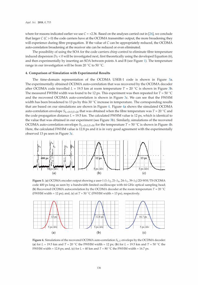
Appl. Sci. 2018, 8, 715
where for reasons indicated earlier we use C = +2.36. Based on the analyses carried out in [26], we concludethat larger C (C > 0) the code carriers have at the OCDMA transmitter output, the more broadening theywill experience during fibre propagation. If the value of C can be appropriately reduced, the OCDMAauto-correlation broadening at the receiver site can be reduced or even eliminated.
The possibility of using the SOA for the code carriers chirp control to eliminate fibre temperatureinduced dispersion DT < 0 will be investigated next, first theoretically using the developed Equation (6),and then experimentally by inserting an SOA between points A and B (see Figure 1). The temperaturerange in our investigation will be from 20 ◦C to 50 ◦C.
4. Comparison of Simulation with Experimental Results
The time-domain representation of the OCDMA USER-1 code is shown in Figure 3a.The experimentally obtained OCDMA auto-correlation that was recovered by the OCDMA decoderafter OCDMA code travelled L = 19.5 km at room temperature T = 20 ◦C is shown in Figure 3b.The measured FWHM width was found to be 12 ps. This experiment was then repeated for T = 50 ◦Cand the recovered OCDMA auto-correlation is shown in Figure 3c. We can see that the FWHMwidth has been broadened to 13 ps by this 30 ◦C increase in temperature. The corresponding resultsthat are based on our simulations are shown in Figure 4. Figure 4a shows the simulated OCDMAauto-correlation envelope SL=19.5;T=20 that was obtained when the fibre temperature was T = 20 ◦C andthe code propagation distance L = 19.5 km. The calculated FWHM value is 12 ps, which is identical tothe value that was obtained in our experiment (see Figure 3b). Similarly, simulations of the recoveredOCDMA auto-correlation envelope SL=19.5;T=50 for the temperature T = 50 ◦C is shown in Figure 4b.Here, the calculated FWHM value is 12.8 ps and it is in very good agreement with the experimentallyobserved 13 ps seen in Figure 3c.
(a) (b) (c)
Figure 3. (a) OCDMA encoder output showing a user-1 (1-λ2, 21-λ4, 24-λ1, 39-λ3) 2D-WH/TS OCDMAcode 400 ps long as seen by a bandwidth limited oscilloscope with 64 GHz optical sampling head;(b) Recovered OCDMA autocorrelation by the OCDMA decoder at the room temperature T = 20 ◦C(FWHM width = 12 ps); and, (c) at T = 50 ◦C (FWHM width = 13 ps), respectively.
(a) (b) (c)
Figure 4. Simulations of the recovered OCDMA auto-correlation SL;T envelope by the OCDMA decoder:(a) for L = 19.5 km and T = 20 ◦C the FWHM width = 12 ps; (b) for L = 19.5 km and T = 50 ◦C theFWHM width = 12.8 ps; and, (c) for L = 40 km and T = 80 ◦C the FWHM width = 16.7 ps.
136

Appl. Sci. 2018, 8, 715
To further emphasise the severity of detrimental effects of temperature induced fiber dispersion,Figure 4c shows the recovered OCDMA auto-correlation envelope S L=40;T=80 simulated for a fiber lengthL = 40 km when exposed to the temperature T = 80 ◦C. The corresponding FWHM value is 16.7 ps.
Our next step was to experimentally investigate a possibility of using the SOA to restore theOCDMA auto-correlation width that is affected by fibre temperature increases to its original valuethat was observed at room temperature, T = 20 ◦C. To conduct this investigation, we inserted an SOA(OPA-20-N-C, Kamelian, Glasgow, UK) at the transmission site between point A and B (see Figure 1).The role of the SOA will be to control the incoming chirp of the code carriers passing through the SOAby changing the bias current, I. This technique is known as a pre-chirping.
Figure 5 shows the experimentally obtained OCDMA auto-correlations that were recovered by theOCDMA decoder when the OCDMA code first passed the biased SOA and then travelled L = 19.5 kmin the transmission link that was exposed at temperature T = 50 ◦C. The OCDMA auto-correlationsthat are shown in Figure 5a–c were obtained for SOA bias currents I = 42 mA, 14 mA, and 8 mA,respectively, and resulted in respective FWHM values of 14 ps, 13 ps, and 12 ps. The loss/gain of SOAw.r.t. the various bias currents have been shown in Figure 6.
(a) I = 42 mA (b) I = 14 mA (c) I = 8 mA
Figure 5. Experimentally recovered OCDMA auto-correlation by the OCDMA decoder for the fibre linktemperature T = 50 ◦C and SOA bias current set to: (a) I = 42 mA (FWHM width = 14 ps); (b) I = 14 mA(FWHM width = 13 ps); and, (c) I = 8 mA (FWHM width = 12 ps), respectively.
Figure 6. SOA Gain vs. Drive Current.
Because transmitting low signal levels can affect the system’s performance and bit error rate(BER), an EDFA-1 on the transmitter site (see Figure 1) was used to amplify the signal.
Figure 7 shows the corresponding simulations of the experimental results that were shown beforein Figure 5 i.e., the recovered OCDMA auto-correlation envelope SL=19.5;T=50 for the OCDMA codepropagation distance L = 19.5 km, fibre link temperature T = 50 ◦C, and chirp value: (a) C = 5 resultingin the FWHM width = 14.2 ps; (b) C = 3 resulting in the FWHM width = 13 ps; and, (c) C = 1 resultingin the FWHM width = 12 ps, respectively.
137

Appl. Sci. 2018, 8, 715
(a) C = 5 (b) C = 3 (c) C = 1
Figure 7. Simulations of the recovered OCDMA auto-correlation envelope SL=19.5;T=50 for OCDMAcode propagation distance L = 19.5 km, T = 50 ◦C, and C equals to (a) 5 resulting FWHM width = 14.2 ps;(b) 3 resulting FWHM width = 13 ps; and, (c) 1 resulting FWHM width = 12 ps, respectively.
Next, we have investigated the cumulative effect of the varying value of the transmission linkGVD (parameter β2) on OCDMA auto-correlation FWHM’s relative changes for the code transmissionin an L = 19.5 km fibre link that was exposed to a temperature of T = 50 ◦C. We have shown (see Figure 8)that the impact of changing β2 (0.03–0.06) ps2/nm (affected by T = 50 ◦C) can also be compensatedusing the SOA by controlling the chirp of OCDMA code carriers.
Figure 8. Compensation of the impact of β2 on OCDMA auto-correlation width changes by using anSOA to control code carriers’ chirp at T = 50 ◦C.
One of the key performance indicators for incoherent OCDMA systems is a power ratio betweenthe recovered auto-correlation peak and cross-correlation noise. In [27], it was shown that this ratio5:1 would worsen to 2.6:1 due to 20 ◦C temperature fluctuations in fibre, thus strongly affecting thesystem BER [28]. As shown in [29], the OCDMA system transmission quality and the BER are affectedby the pulse shape. As such, a skewed pulse profile of the recovered OCDMA auto-correlation willalso impact the system BER and the overall system performance.
5. Discussion
Our recent work has been focused on the application of SOAs for improving the performance ofincoherent OCDMA systems that are based on a 2D-WH/TS coding scheme using multi-wavelengthpicosecond code carriers. In [19], we reported for the first time the use of an SOA on the receiver site tocontinuously compensate for the broadening of the OCDMA auto-correlation due to the temperatureinduced dispersion in the optical fibre (the temperature induced dispersion coefficient DT < 0 inSMF-28). The SOA compensation was applied directly on the distorted OCDMA auto-correlationcomposed of multi-wavelength code carriers sitting on top of each other. We have shown that thebroadening of the OCDMA auto-correlation width due to the fibre temperature induced dispersioncan be mitigated using the twin SOA by controlling its chirp through bias current adjustments once
138

Appl. Sci. 2018, 8, 715
the OCDMA auto-correlation is recovered by the OCDMA decoder. In [18], we investigated the useof an SOA that was also placed on the receiver site for a continuous manipulation of the broadenedOCDMA auto-correlation due to fibre link CD (chromatic dispersion coefficient DCD > 0 in SMF-28).The SOA compensation was applied directly on the distorted OCDMA auto-correlation composedof four multi-wavelength code carriers sitting on top of each other. In this configuration, we hadto use a picosecond optical pulse called a holding beam (OP/HB) synchronized with the OCDMAauto-correlation at the SOA input to be able to demonstrate that the OCDMA auto-correlation that wasbroadened by the fibre chromatic dispersion can be continuously ‘compressed’. In [20], we reportedthe use of an SOA on the transmitter site (right after the OCDMA encoder) to compensate the OCDMAauto-correlation broadening due to the fibre chromatic dispersion (DCD > 0), we observed on theOCDMA receiver site by controlling the chirp of the individual multi-wavelength OCDMA codecarriers spread over a bit period before the code is launched into a fibre link.
In this paper, we have investigated for the first time how controlling the chirp of the OCDMAcode carriers by the SOA prior to entering the fibre transmission link that was exposed to varyingtemperature (20 ◦C to 50 ◦C) will influence the recovered OCDMA auto-correlation and its width at thereceiver site. We have shown both experimentally and by using simulations that the distorted OCDMAauto-correlation due to temperature induced fibre dispersion (DT < 0) can be corrected by manipulatingthe chirp of OCDMA code carriers when traversing the biased SOA before entering the transmissionlink. In addition, the effects of varying values of GVD (parameter β2) on the OCDMA auto-correlationwidth were also investigated. We have shown that the impact of a changing β2 (0.03–0.06) ps2/nmwhen the fibre link was exposed to 50 ◦C could be compensated by controlling the code carriers’ chirpby placing an SOA on the transmitting site. Our simulation results are in very good agreement withexperimental observations.
6. Conclusions
The real communication systems that were operating under changing environmental conditionsmay experience temperature variations along the transmission link. These variations may not beuniform and would locally change the transmission link properties. The local temperature changeswill inflict local GVD changes, which in turn will cause deviations from the ‘originally designed steadystate’ fibre dispersion compensation. Since the dispersion is a cumulative effect, it will manifest itselfat the receiving end as a time and temperature varying disturbance. To mitigate it would require todynamically control the SOA.
Author Contributions: I.G. conceived and designed the experiments; contributed to data analyses and writing thepaper; supervised the research work; Md.S.A. performed the experiments; contributed to data analyses; designedthe analysing tools; contributed to writing the paper.
Acknowledgments: This work was supported by the European Union’s Horizon 2020 Research and InnovationProgram through the Marie Sklodowska-Curie under Grant 734331.
Conflicts of Interest: The authors declare no conflict of interest. The funding sponsors had no role in the designof the study; in the collection, analyses, or interpretation of data; in the writing of the manuscript, and in thedecision to publish the results.
References
1. Willner, A.E.; Hoanca, B. Fixed and tunable management of fiber chromatic dispersion. In Optical FiberTelecommunications IV-B, 4th ed.; Elsevier: New York, NY, USA, 2002; pp. 642–724.
2. Norgard, G. Chromatic Dispersion Compensation: Extending Your Reach. Available online: http://www.datacenterjournal.com/chromatic-dispersion-compensation-extending-reach/ (accessed on 25 March 2018).
3. Singh, M. Different dispersion compensation techniques in fiber optic communication system: A survey.Int. J. Adv. Res. Electron. Commun. Eng. 2015, 4, 2236–2240.
4. Karar, A.S.; Cartledge, J.C.; Harley, J.; Roberts, K. Electronic pre-compensation for a 10.7-Gb/s systememploying a directly modulated laser. J. Lightwave Technol. 2011, 29, 2069–2076. [CrossRef]
139

Appl. Sci. 2018, 8, 715
5. Yang, G.C.; Kwong, W.C. Prime Codes with Applications to CDMA Optical and Wireless Networks; Artech House:Boston, MA, USA, 2002.
6. Tanceski, L.; Andonovic, I. Wavelength hopping/time spreading code division multiple access systems.Electron. Lett. 1994, 30, 1388–1390. [CrossRef]
7. Yegnanarayanan, S.; Bhushan, A.S.; Jalali, B. Fast wavelength-hopping time-spreading encoding/decodingfor optical CDMA. IEEE Photon. Technol. Lett. 2000, 12, 573–575. [CrossRef]
8. Glesk, I.; Prucnal, P.R.; Andonovic, I. Incoherent ultrafast OCDMA receiver design with 2 ps all-opticaltime gate to suppress multiple-access interference. IEEE J. Sel. Top. Quantum Electron. 2008, 14, 861–867.[CrossRef]
9. Dang, N.T.; Pham, A.T.; Cheng, Z. Impact of GVD on the performance of 2-D WH/TS OCDMA systems usingheterodyne detection receiver. IEICE Trans. Fundam. Electron. Commun. Comput. Sci. 2009, 94, 1182–1191.[CrossRef]
10. Ng, E.K.; Weichenberg, G.E.; Sargent, E.H. Dispersion in multiwavelength optical code-divisionmultiple-access systems: Impact and remedies. IEEE Trans. Commun. 2002, 50, 1811–1816. [CrossRef]
11. Idris, S.K.; Osadola, T.B.; Glesk, I. Investigation of all-optical switching OCDMA testbed under the influenceof chromatic dispersion and timing jitter. J. Eng. Technol. 2013, 4, 51–65.
12. Eggleton, B.J.; Ahuja, A.; Westbrook, P.S.; Rogers, J.A.; Kuo, P.T.; Nielsen, N.; Mikkelsen, B. Integrated tunablefiber gratings for dispersion management in high-bit rate systems. J. Lightwave Technol. 2000, 18, 1418–1432.[CrossRef]
13. Tanizawa, K.; Hirose, A. Adaptive control of tunable dispersion compensator that minimizes time-domainwaveform error by steepest descent method. IEEE Photon. Technol. Lett. 2006, 18, 1466–1468. [CrossRef]
14. Sano, A.; Kataoka, T.; Tomizawa, M.; Hagimoto, K.; Sato, K.; Wakita, K.; Kato, K. Automatic dispersionequalization by monitoring extracted-clock power level in a 40-Gbit/s, 200-km transmission line. In Proceedingsof the 22nd European Conference on Optical Communication, Oslo, Norway, 19 September 1996; Volume 2,pp. 207–210.
15. Ooi, H.; Nakamura, K.; Akiyama, Y.; Takahara, T.; Terahara, T.; Kawahata, Y.; Isono, H.; Ishikawa, G.40-Gb/s WDM transmission with virtually imaged phased array (VIPA) variable dispersion compensators.J. Lightwave Technol. 2002, 20, 2196–2203.
16. Neilson, D.T. Advanced MEMS devices for channelized dispersion compensation. In Proceedings of theOptical Fiber Communications Conference (OFC2004), Los Angeles, CA, USA, 22 February 2004; Volume 1.
17. Wielandy, S.; Westbrook, P.S.; Fishteyn, M.; Reyes, P.; Schairer, W.; Rohde, H.; Lehmann, G. Demonstration ofautomatic dispersion control for 160 Gbit/s transmission over 275 km of deployed fibre. Electron. Lett. 2004,40, 690–691. [CrossRef]
18. Ahmed, M.S.; Abuhelala, M.S.K.; Glesk, I. Managing dispersion-affected OCDMA auto-correlation based onPS multiwavelength code carriers using SOA. IEEE/OSA J. Opt. Commun. Netw. 2017, 9, 693–698. [CrossRef]
19. Ahmed, M.S.; Glesk, I. Mitigation of temperature induced dispersion in optical fiber on OCDMAauto-correlation. IEEE Photon. Technol. Lett. 2017, 29, 1979–1982. [CrossRef]
20. Ahmed, M.S.; Glesk, I. Management of OCDMA auto-correlation width by chirp manipulation using SOA.IEEE Photon. Technol. Lett. 2018, 30, 785–788. [CrossRef]
21. Huang, J.F.; Yang, C.C. Reductions of multiple-access interference in fiber-grating-based optical CDMAnetwork. IEEE Trans. Commun. 2002, 50, 1680–1687. [CrossRef]
22. Kato, T.; Koyano, Y.; Nishimura, M. Temperature dependence of chromatic dispersion in various types ofoptical fiber. Opt. Lett. 2000, 25, 1156–1158. [CrossRef] [PubMed]
23. Agrawal, G.P. Nonlinear Fiber Optics; Academic Press: Cambridge, MA, USA, 2007.24. Osadola, T.B.; Idris, S.K.; Glesk, I.; Kwong, W.C. Effect of variations in environmental temperature on
2D-WH/TS OCDMA code performance. J. Opt. Commun. Netw. 2013, 5, 68–73. [CrossRef]25. Wright, E.M. Module 3–Numerical Pulse Propagation in Fibers. Available online: http://data.cian-erc.org/
supercourse/Graduatelevel/module_3/3_SC_GRAD_LEVEL_Module3_wright.pdf (accessed on 25 March 2018).26. Abramczyk, H. Dispersion Phenomena in Optical Fibers. Virtual European University on Lasers.
Available online: http://www.mitr.p.lodz.pl/evu/wyklady/ (accessed on 25 March 2018).
140

Appl. Sci. 2018, 8, 715
27. Tsai, C.Y.; Yang, G.C.; Lin, J.S.; Chang, C.Y.; Glesk, I.; Kwong, W.C. Pulse-power-detection analysis ofincoherent O-CDMA systems under the influence of fiber temperature fluctuations. J. Lightwave Technol.2017, 35, 2366–2379. [CrossRef]
28. Majumder, S.P.; Azhari, A.; Abbou, F.M. Impact of fiber chromatic dispersion on the BER performance of anoptical CDMA IM/DD transmission system. IEEE Photon. Technol. Lett. 2005, 17, 1340–1342. [CrossRef]
29. Islam, M.J.; Halder, K.K.; Islam, M.R. Effect of optical pulse shape on the performance of OCDMA in presenceof GVD and pulse linear chirp. Int. J. Comput. Sci. Eng. 2010, 2, 1041–1046.
© 2018 by the authors. Licensee MDPI, Basel, Switzerland. This article is an open accessarticle distributed under the terms and conditions of the Creative Commons Attribution(CC BY) license (http://creativecommons.org/licenses/by/4.0/).
141


MDPISt. Alban-Anlage 66
4052 Basel
SwitzerlandTel. +41 61 683 77 34Fax +41 61 302 89 18
www.mdpi.com
Applied Sciences Editorial OfficeE-mail: [email protected]
www.mdpi.com/journal/applsci


MDPI St. Alban-Anlage 66 4052 Basel Switzerland
Tel: +41 61 683 77 34 Fax: +41 61 302 89 18
www.mdpi.com ISBN 978-3-03897-171-9