
Integrated Optical Carrier for Optical/Electrical Interconnect

JOURNAL OF LIGHTWAVE TECHNOLOGY, VOL. 27, NO. 6, MARCH 15, 2009 631
All-Optical Label Swapping Using BistableSemiconductor Ring Laser in an
Optical Switching NodeKornkamol Thakulsukanant, Student Member, IEEE, Bei Li, Irfan Memon, Gabor Mezosi, Zhuoran Wang,
Marc Sorel, Member, IEEE, and Siyuan Yu, Member, IEEE
Abstract—This paper demonstrates an optical node that simul-taneous carries out multicast optical switching and all-optical labelswapping. While the optical payload is being forwarded by a fastoptical switch matrix, the optical label is processed by a semicon-ductor ring laser (SRL) bistable. Old address bits in the label areerased by optically blocking the switching of the ring laser and newaddress bits are inserted by modulating the output from SRL di-rectly. This label swapping scheme is the first demonstration ofbit-level data processing using the all-optical logic capabilities ofa semiconductor ring laser.
Index Terms—Optical crosspoint switch, optical label swapping,optical label switching, semiconductor ring laser.
I. INTRODUCTION
D UE TO tremendous growth of the internet traffic duringthe recent years, improvement on all performances such
as speed, capacity, and packet forwarding rates of next gener-ation Internet Protocol (IP) networks is necessary. Many tech-nologies based on all-optical networking have been explored inorder to support the scalability of terabit rates packet routing andnew streamlined IP routing protocol e.g., multiprotocol labelswapping (MPLS) [1].
All-optical label processing functions such as label swappingis essential for reducing the complexity and cost of the opticalswitching nodes by moving processing to the optical domain inoptical label switching (OLS) networks. Many technologies foroptical label swapping have been investigated so far, includingthose based on wavelength conversion [2]–[15], optical logicgates and flip-flop [16], [17]. Optical label swapping techniquesstrongly relate to optical label coding schemes such as serial-bitlabeling [5], subcarrier multiplexing [2], [3], [6], and orthogonalmodulation labeling [18], [19]. Various approaches to opticallabel swapping for resolving the dispersion induced fading androuter packet forwarding capacity are proposed [2]. A research
Manuscript received January 18, 2008; revised April 13, 2008. Current ver-sion published April 17, 2009. The work of K. Thakulsukanant was supportedby Assumption University, Bangkok, Thailand, and the Thai Government.
K. Thakulsukanant, B. Li, I. Memon, Z. Wang, S. Yu, and S. Mezosi arewith the Department of Electrical and Electronic Engineering, Universityof Bristol, Bristol BS8 1UB, U.K. (e-mail: [email protected];[email protected]; [email protected]; [email protected];[email protected]).
G. Mezosi and M. Sorel are with the Department of Electrical and Elec-tronic Engineering, University of Glasgow, Glasgow G12 8LT, U.K. (e-mail:[email protected]; [email protected]).
Color versions of one or more of the figures in this paper are available onlineat http://ieeexplore.ieee.org.
Digital Object Identifier 10.1109/JLT.2008.927755
team at University of California Davis demonstrated label swap-ping and 2R generation [6]–[11], 101-hop cascaded OLS withclock recovery and 3R generation [13], and optical time-to-live(TTL)-based optical selective-3R in OLS router [14] with errorfree operations. Transmission and optical label swapping forASK payload and DPSK label by using dc-balanced 8B10Bcoding with an overall power penalty of 3.3 dB for payload and0.3 dB for label was reported in [15]. Apart from the two maintechniques mentioned above, [20], [21] also presented two dif-ferent ways of all-optical label swapping without requiring con-ventional wavelength converter. These techniques were basedon using optical single-sideband modulation and optical notchfilter. In [20] the old subcarrier was suppressed by 25 dB butburst mode payload experienced only 2 dB power penalty. In[21] optical carrier suppression and separation (OCSS) withpower penalty below 2 dB at BER for both payload andlabel is demonstrated.
Much work on all-optical logic gates and flip-flops have beenbased on semiconductor optical amplifier Mach–Zehnder inter-ferometer (SOA-MZI) which can provide output signal extinc-tion ratio of dB [16], with fast switching speed capable of40 Gb/s processing [22].
On the other hand, semiconductor ring laser (SRL) has re-ceived increasing attention recently because of its bistabilitycharacteristics between the clockwise (CW) and counterclock-wise (CCW) propagating directions [23]. SRLs have demon-strated potentials for all-optical switching [24], pulse regener-ation, and optical memory [25] and therefore it is a promisingcandidate for all-optical label processing applications.
In this paper, we demonstrate a novel optical label swap-ping scheme as part of an optical switching node using all-optically controlled optical flip-flop based on a 4-port mono-lithic semiconductor ring laser (SRL). The paper is organizedas follows: Principles and structures of the SRL and active ver-tical coupler crosspoint switch (AVC-OXS) devices are pro-vided in Section II. Section III presents details of the experi-mental setup for optical label swapping using SRL and opticalpacket switching based on AVC OXS matrix. The results are de-scribed in Section IV. Finally, Section V presents conclusionsand discussions.
II. PRINCIPLES AND STRUCTURES OF SRL AND OXS
A. Semiconductor Ring Laser
A monolithic 4-port SRL device, which was fabricatedon a multiple quantum well (MQW) AlGaInAs/InP wafer
0733-8724/$25.00 © 2009 IEEE

632 JOURNAL OF LIGHTWAVE TECHNOLOGY, VOL. 27, NO. 6, MARCH 15, 2009
Fig. 1. Photograph of the 4-port SRL device.
Fig. 2. L–I curve measured for both directions of the SRL.
at Glasgow University, has a structure shown in Fig. 1. Theracetrack shaped ring cavity has two semi-circular sectionswith 150 m radius and two 185 m long straight sections.Two access waveguides are coupled to the ring cavity byforming directional couplers with the 185 m straight sections,providing % coupling ratio. The access waveguides form a10 degree angle with the cleaved bar facet to minimize back-re-flection. As shown in Fig. 2, this device has been tested with acontinuous wave threshold of 45 mA at 17.5 C. Above 57 mA,uni-directional operation or directional bistability appears in the
– curve where the laser operates either in the CW or CCWdirection. A directional extinction ratio of dB is measuredfor currents above 110 mA. As demonstrated in [24]–[28], suchdirectional bistability can be employed to realize all-opticalflip-flop, all-optical logic inverter, and all-optical data gating.Furthermore, the response of SRL to two optical injections inopposite directions demonstrates a typical bistable hysteresisloop [29], with the switch-on and -off thresholds as well as thewidth of the hysteresis in one injection direction controllableby the power of injection in the opposite direction. This char-acteristic forms the basis of our label erasure scheme. In ourexperiment, the device is biased at 120 mA. For this relativelylarge device, the switching time between the two directions is
ns.
B. Optical Crosspoint Switch (OXS)
The active vertical coupler (AVC) optical cross point switch isa 4 4 matrix switch, integrated on an InP substrate. It consistsof two perpendicular groups of passive ridge waveguides repre-senting the input and output data paths of the OXS as shown inFig. 3, [30], [31]. Two AVCs are formed at each crosspoint ofthe switch by stacking active waveguides on top of both input
Fig. 3. (a) OXS matrix structure. (b) Schematic diagram for OXS matrix.
Fig. 4. (a) Single switch cell on-state. (b) Single switch cell-off state.
and output passive waveguides. A total internal reflection (TIR)mirror cuts vertically through the active waveguide and diag-onally across the waveguide intersection. This allows a 90 de-flection of the optical signal from AVC1 to AVC2 as shown inFig. 3(a).
In the ON state, when the current injection is applied, theeffective reflective index of the upper waveguide is reduced tomatch that of the lower waveguide to allow strong coupling ofthe input signal. Once the optimum coupling has been satisfied,the optical input signal is completely coupled via the AVCs andexported to the output, in the same time being amplified by theoptical gain in the active layer as shown in Fig. 4(a).
In the OFF state, no current injection being applied, there issignificant difference of the effective refractive index betweenthe upper active and lower passive waveguides, which resultsin very low coupling. The input signal is forwarded to the nextswitch cell along the input passive waveguide as shown inFig. 4(b).
The OXS matrix has a compact size of 500 500 m percell, a fast chip-switching speed of ns, and extremely lowcrosstalk levels of dB [30], [32]. Due to high fiber cou-pling loss, the device has a fiber-to-fiber insertion loss of about
20 dB despite some optical gain provided by the chip.

THAKULSUKANANT et al.: ALL-OPTICAL LABEL SWAPPING USING BISTABLE SEMICONDUCTOR RING LASER IN AN OPTICAL SWITCHING NODE 633
Fig. 5. A simplify block diagram for the experiment. (Dash lines: electricalsignals; solid lines: optical signals through out the context).
Fig. 6. Timing diagram of the label and payload packet in one time slot.
III. EXPERIMENTAL SETUP
The switch node as shown in Fig. 5 has three parts, an elec-tronic control circuit, an optical payload router and an opticallabel swapping part. The optical label swapping part is mainlybased on the SRL device, and the optical payload routing is per-formed by the AVC-OXS matrix.
The optical data to be processed by the node consists of a10 Gb/s payload packet and a label as a time-serial header. Thelabel and the payload are modulated on two wavelengths. The16-bit label pattern has a a data rate of 155 Mb/s and a wave-length coinciding with the first short wavelength side modeof the SRL. The label signal is used to operate OXS cells viathe electronic control. The 155-Mb/s label data rate is used todemonstrate the principles of label swapping considering the
1-ns switching time of the SRL. The packet payload is a 10Gb/s pseudorandom binary sequence (PRBS) of length at1550 nm, with a packet length of 103.2 ns. The payload is lag-ging 193.5 ns behind the label signal, including 103.2-ns labellength and 90.3-ns guard time to accommodate the risingedge of the switching window. Above optical data is repeatedlytransmitted every 1.2 s. Fig. 6 shows the timing diagram be-tween the label and payload in a time slot.
In this scheme, there is no need for particular arrangementfor label/payload separation. In the label swapping (erasure andreinsertion) part, the payload is filtered out by the SRL be-cause SRL only respond to certain wavelengths (coinciding withtheir modes), in this case the label wavelength is one of thesewavelengths and payload wavelength is not. In the label detec-tion/control part, the 155 Mb/s PINFET does not respond to10 Gb/s payload. In the payload switching part, the old label
Fig. 7. Setup details for optical packet switching based on OXS matrix.
is removed by the crosspoint switch because the switch is onlyturned on during the payload.
Referring to Fig. 5, a label signal is divided into two parts viaa 10-dB coupler. The low power branch of the signal is appliedto a 155-Mb/s PINFET, which converts the incoming label toelectronic form for the electronic control to decode. The controlcircuit generates two individual electrical signal pulses. One isthe switching window pulse that controls the payload routing.Another one is an electrical label erasure pulse controlling thelabel processing.
The payload routing part is a simple optical packet switchbased on the AVC-OXS matrix as shown in Fig. 7. The switchingcurrent to the appropriate cell is turned on by the switchingwindow pulse, which is generated by decoding the address codein the label. Erbium doped fiber amplifiers (EDFA4 and EDFA5)are used to amplify the input and the output packet to boost inputdata power and to compensate fiber-fiber insertion loss of theOXS device. An optical bandpass filter (BPF3) is used to reduceaccumulated ASE noise in the signal at the final output beforebeing displayed by the digital communication analyzer (DCA).Polarisation controller (PC7) on input port is also essential dueto the OXS has polarisation dependence of dB.
The setup for the label swapping part is shown in Fig. 8, withthe SRL at its center. The SRL is powered by a dc current of 120mA and its temperature is controlled at 17.5 C. The high powerbranch from the 10-dB coupler is applied to port 1 of SRL as theoptical label input to be processed. EDFA1 and a variable opticalattenuator (VOA1) are used for adjusting the input optical labelpower into SRL port 1 to balance the power during label swap-ping against the optical erasure pulse. The optical erasure pulseat a wavelength coinciding with the main mode of the SRLis generated by modulating tunable laser TL2 with the electricallabel erasure pulse, and is applied to port 3 of the SRL, againwith its power adjusted by EDFA2 and VOA2. A fiber delay line(FDL) is used to match the delay between the label data and op-tical erasure pulse. Polarisation controllers (PC3 and PC4) areused at both input ports to maintain TE output. The optical era-sure pulse is expected to block the transmission of the opticallabel through the SRL to ports 2 and 4. The erasure process isdescribed in detail in the next section. Ports 2 and 4 are the twologically complementary outputs of the SRL bistable. A 10-Gb/sPINFET is used to convert the optical output at both ports toelectrical signal. DCA and an optical spectrum analyzer (OSA)

634 JOURNAL OF LIGHTWAVE TECHNOLOGY, VOL. 27, NO. 6, MARCH 15, 2009
Fig. 8. Setup details for optical label swapping part.
are used to observe outputs in both time and frequency domains,respectively.
The output from port 4 of the SRL is the logically invertedlabel output with the address bits erased—i.e., all address bitsare set to high level. This is modulated by the new label addressbits in order to generate a new label with the new address in-serted. EDFA3 is used to boost the power of the output fromport 4. Its ASE noise is filtered by the optical bandpass filter(BPF1).
IV. RESULTS AND DISCUSSION
A. Label Detection and Electronic Control
The 16-bit optical label pattern “1100110011110001” con-sists of 6 bits of header (110011), 1 idle bit (0), 8 address bits(01111000), and 1 ending bit. The header bits are used as a labelarrival recognition pattern for operating the electronic control.The idle is used to separate the header bits and the address bits.The address bits correspond to the address of the 16 cells of OXSmatrix. The first 4 bits (0111) and the last 4 bits (1000) indicatethe column (W–Z) and the row (1–4) address of the OXS matrixrespectively, as shown in Fig. 3(b) in Section II. To operate anOXS cell, the corresponding column and row address bits bothhave to be “1”. Thus, the 8 address bits of “01111000” will turnon 3 switch cells of 1X–1Z in the OXS matrix, which is an mul-ticast configuration [33], [34]. Changing the address bit patternin the label changes the scale and configuration of the multicast.Fig. 9 shows the optical label input and electrical label outputbefore and after 155-Mb/s PINFET.
The electronic control circuit is mainly a complex pro-grammable logic device (CPLD) programmed to decode theinput label from the 155-Mb/s PINFET and to generate boththe switching window and address erasure pulse. A switchingwindow of 245.1 ns (38 bits) is used to turn on the OXScell. Electrical current pulses corresponding to the switchingwindow is applied to the three switch cells by the OXS drivercircuit. The erasure pulse of 64.5 ns (10 bits) long is aimed to
Fig. 9. 16-bits optical label. (a) Optical data before 155-Mb/s PINFET(vertical scale = 20 �w/div). (b) Output from 155-Mb/s PINFET(vertical = 100 mv/div).
Fig. 10. (a) Switching window of 245.1 ns for operating OXS matrix and(b) erasure pulse of 64.5 ns for SRL. vertical scale = 100 mv/div.
delete the last 9 bits of the label signal (011110001) includingthe 8 address bits for controlling the OXS matrix and the endingbit. Fig. 10 shows the electrical outputs of switching windowsand erasure pulse created by the CPLD.
B. Label Erasure, Swapping, and Optical Packet Switching
Referring to Fig. 8 in Section III, two optical signals of labeldata and erasure pulse are applied to ports 1 and 3 of the SRL,respectively. Matching of the delay between the two inputs isessential before further processing. Fig. 11 shows the delaymatched waveforms at port 1 and 3.
The label erasure process relies on the switching of SRLlasing directions triggered by optical injection resonant to SRL

THAKULSUKANANT et al.: ALL-OPTICAL LABEL SWAPPING USING BISTABLE SEMICONDUCTOR RING LASER IN AN OPTICAL SWITCHING NODE 635
Fig. 11. Delay matched waveform of both label (� ) and erasure pulse (� ).Vertical = 100 mv/div.
modes. Such an injection will lock the SRL to the injecteddirection and wavelength as demonstrated in [26].
The optical erasure pulse is adjusted so that it has a limitedextinction ratio, i.e., it has some power when erasure pulse is“low.” When there is no label input, this injection power “bi-ases” the SRL in the CCW direction [27] as an optical monos-table and locks the SRL lasing wavelength at the erasure pulsewavelength which is aligned to a SRL cavity mode wave-length as shown in Fig. 12(a). This shows the port 2 output spec-trum locked to erasure pulse wavelength .
During the 16 label bits, when the optical erasure pulse is“low,” each “1” bit in the label signal is adjusted to have suf-ficient power to be able to switch the SRL monostable to theCW direction and to the label pulse wavelength of . Betweenthese “1” bits, the SRL reverts back to the CCW direction andthe wavelength of due to the presence of the low power at
. The label bits therefore are transmitted through the SRL byswitching the SRL direction and wavelength, and at ports 2 and4 logically complementary outputs are obtained at andrespectively.
When the optical erasure pulse arrives, which coincides withthe last 9 address bits of the label signal to be erased, its highpower exceeds the switching threshold for the label bits, pre-venting the SRL from being flipped by the “1” bits in the labeladdress, and thus, blocking the transmission of the label throughthe SRL. Therefore, label erasure is realized as shown in Fig. 13with the two complementary outputs. The two VOAs and twoPCs at both input ports are adjusted in order to obtain the bestlabel erasure outputs. The power level relationship between thetwo input ports can be found from experimental data reportedin [29], where the input power of one input will change the re-sponse of the SRL to another input in terms of both its switchingthresholds and minimum required extinction ratio (ER) to com-plete switching both from CW to CCW and vise versa. In thislabel swapping experiment, the erasure pulse is equivalent to theholding beam in [29]. When it is “low,” the label input needs aminimum ER of dB to operate. When it is high, the switchingthreshold for the label input is raise above the “1” level of thelabel signal, so no switching is possible.
Fig. 12. (a) Spectrum of mode locking on erasure pulse from port 2. (b) Spec-trum of mode locking on both label signal and erasure pulse from the same port.
Fig. 13. (a) Output of label erasure waveform from port 2, with only the first 7bits of “1100110” left in the label, and (b) The complementary output of labelerasure from port 4. Vertical scale: 10 mv/div. (Erasure pulse power = 7 dBmand label power = 3 dBm).
The label erasure outputs from both output ports 2 and 4 areshown in Fig. 13. The performance of the label erasure can becharacterized by a suppression ratio, which is calculated as ratio
636 JOURNAL OF LIGHTWAVE TECHNOLOGY, VOL. 27, NO. 6, MARCH 15, 2009
Fig. 14. Inverted label swapping signal from port 4. Vertical scale: 10 mv/div.
Fig. 15. Output packet of Z1 cell while label erasure is performed.Vertical scale = 500 �w/div.
of the amplitude of unsuppressed data bits over that of the sup-pressed bits. The positive logic output 2 has a suppression ratioof about 15 dB, and the logically inverted output 4 has a sup-pression ratio of dB due to the fluctuations at the high levelwhere the address bits are erased. Moreover, an extinction ratioof dB is obtained in the pass through bits.
Fig. 12(b) shows a time-averaged output spectrum from thesame output port 2 during normal label erasure operation. TheSRL is now working alternatively in the CW and CCW direc-tions. The side mode at is slightly raised due to the fact thatsometimes the SRL operates at . But because when the SRLoperates at and CW direction, its output power is emittedmainly at port 4, what’s observed at port 2 is just a small amountof reflection of the mode superimposed with the still domi-nant CCW mode.
With the output of inverted label minus the address bit fromport 4, 9 new bits of label address code “011000111” are rein-serted to replace all the erased old address bits. This is simplycarried out by modulating the port 4 output by means of MZM3with these new bits as shown in Fig. 8 in Section III. EDFA 3is used to re-boost the power level of the signal and BPF1 isused to suppress ASE noise. Finally, 16 bits of an inverted op-tical label with swapped address code “1100110011000111” isobtained as shown in Fig. 14.
While label erasure is being performed, the optical payloadswitching based on AVC OXS matrix is also in operation. Re-ferring to Section IV-A, three switch cells of the OXS matrix(1X–1Z) are now in action. The output packet at 1Z is moni-tored and shown in Fig. 15. The length of the packet is 103.2 ns,which fits within switching current window of 245.1 ns.
C. SRL Output Signal Quality
In order to verify the output label signal quality of the SRL,back-back (B-B) and SRL-transmitted bit-error rate test hasbeen carried out. Although the data rate is 155 Mb/s, the testsare carried out with a 10 Gbit/s PINFET receiver (hence the
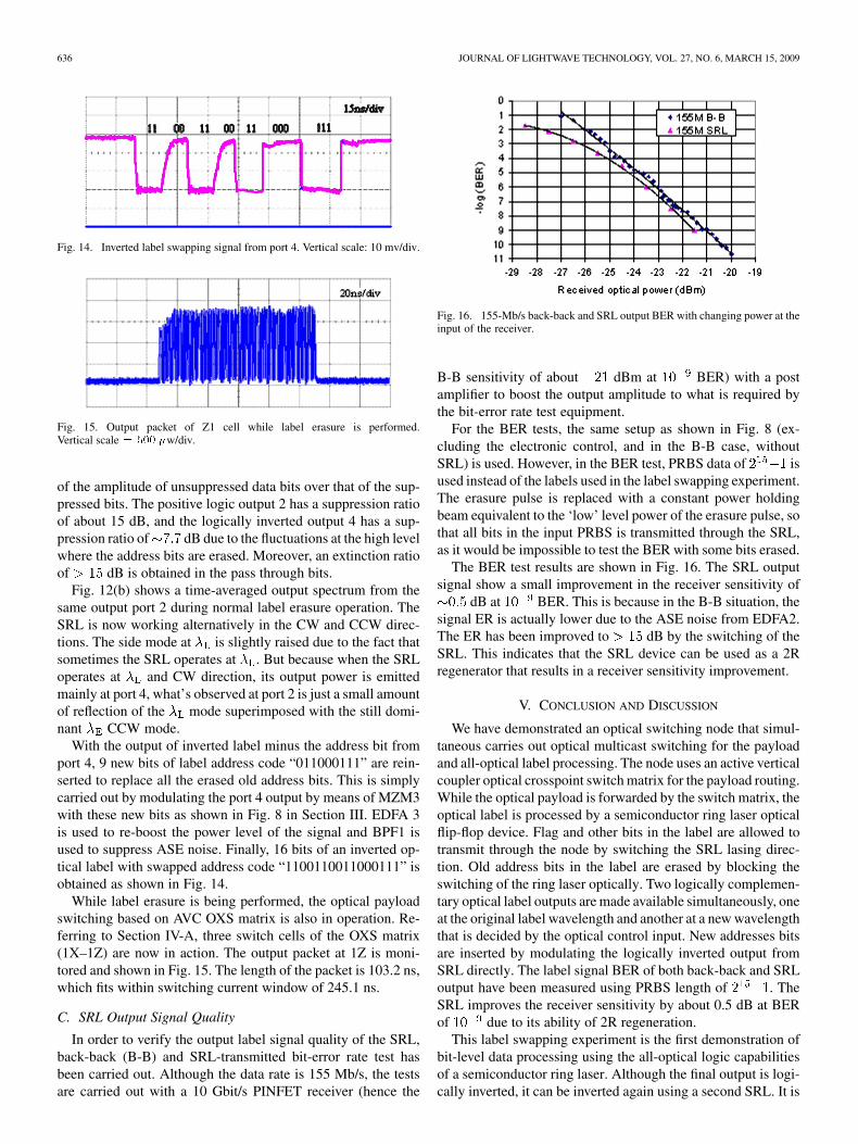
Fig. 16. 155-Mb/s back-back and SRL output BER with changing power at theinput of the receiver.
B-B sensitivity of about dBm at BER) with a postamplifier to boost the output amplitude to what is required bythe bit-error rate test equipment.
For the BER tests, the same setup as shown in Fig. 8 (ex-cluding the electronic control, and in the B-B case, withoutSRL) is used. However, in the BER test, PRBS data of isused instead of the labels used in the label swapping experiment.The erasure pulse is replaced with a constant power holdingbeam equivalent to the ‘low’ level power of the erasure pulse, sothat all bits in the input PRBS is transmitted through the SRL,as it would be impossible to test the BER with some bits erased.
The BER test results are shown in Fig. 16. The SRL outputsignal show a small improvement in the receiver sensitivity of
dB at BER. This is because in the B-B situation, thesignal ER is actually lower due to the ASE noise from EDFA2.The ER has been improved to dB by the switching of theSRL. This indicates that the SRL device can be used as a 2Rregenerator that results in a receiver sensitivity improvement.
V. CONCLUSION AND DISCUSSION
We have demonstrated an optical switching node that simul-taneous carries out optical multicast switching for the payloadand all-optical label processing. The node uses an active verticalcoupler optical crosspoint switch matrix for the payload routing.While the optical payload is forwarded by the switch matrix, theoptical label is processed by a semiconductor ring laser opticalflip-flop device. Flag and other bits in the label are allowed totransmit through the node by switching the SRL lasing direc-tion. Old address bits in the label are erased by blocking theswitching of the ring laser optically. Two logically complemen-tary optical label outputs are made available simultaneously, oneat the original label wavelength and another at a new wavelengththat is decided by the optical control input. New addresses bitsare inserted by modulating the logically inverted output fromSRL directly. The label signal BER of both back-back and SRLoutput have been measured using PRBS length of . TheSRL improves the receiver sensitivity by about 0.5 dB at BERof due to its ability of 2R regeneration.
This label swapping experiment is the first demonstration ofbit-level data processing using the all-optical logic capabilitiesof a semiconductor ring laser. Although the final output is logi-cally inverted, it can be inverted again using a second SRL. It is

THAKULSUKANANT et al.: ALL-OPTICAL LABEL SWAPPING USING BISTABLE SEMICONDUCTOR RING LASER IN AN OPTICAL SWITCHING NODE 637
also possible to convert the wavelength of the new label to anyother wavelength supported by the SRL cavity, using the sameprocess. For our experiment the label insertion still relied on anoptical modulator, however it is also possible to perform the in-sertion all-optically using a second SRL should the new addressbits to be inserted arrive optically.
This experiment serves as a first demonstration of principlesfor similar all-optical processing using the SRL. Although thedata rate is limited by the switching time of the large SRL devicecurrently available, smaller SRLs, which was reported in [35],will be able to switch sufficiently fast to enable multi-giga bitoperations.
ACKNOWLEDGMENT
The authors would like to thank Dr. P. Jiang for providingvery useful suggestions and encouragement during the work.
REFERENCES
[1] A. Viswanathan, N. Feldman, Z. Wang, and R. Callon, “Evolution ofmultiprotocol label switching,” IEEE Commun. Mag., vol. 36, no. 5,pp. 165–173, May 1998.
[2] D. J. Blumenthal, B.-E. Olsson, G. Rossi, T. E. Dimmick, L. Rau,M. Masanovic, O. Lavrova, R. Doshi, O. Jerphagnon, J. E. Bowers,V. Kaman, L. A. Coldren, and J. Barton, “All-optical label swappingnetworks and technologies,” J. Lightw. Technol., vol. 18, no. 12, pp.2058–2075, Dec. 2000.
[3] D. J. Blumenthal, A. Carena, L. Rau, V. Curri, and S. Humphries, “All-optical label swapping with wavelength conversion for WDM-IP net-works with subcarrier multiplexed addressing,” IEEE Photon. Technol.Lett., vol. 11, no. 11, pp. 1497–1499, Nov. 1999.
[4] A. Carena, M. D. Vaughn, R. Gaudino, M. Shell, and D. J. Blumen-thal, “OPERA: An optical experimental routing architecture withlabel swapping capability,” J. Lightw. Technol., vol. 16, no. 12, pp.2135–2145, Dec. 1998.
[5] B.-E. Olsson, P. Öhlén, L. Rau, G. Rossi, O. Jerphagnon, R. Doshi, D.S. Humphries, D. J. Blumenthal, V. Kamann, and J. E. Bowers, “Wave-length routing of 40 Gbit/s packets with 2.5 Gbit/s header erasure/rewriting using all-fibre wavelength converter,” Electron. Lett., vol. 36,no. 4, pp. 345–347, Feb. 2000.
[6] M. Y. Jeon, Z. Pan, J. Cao, Y. Bansal, J. Taylor, Z. Wang, V. Alkella,K. Okamoto, S. Kamei, J. Pan, and S. J. B. Yoo, “Demonstration ofall-optical packet switching routers with optical label swapping and 2Rregeneration for scalable optical label switching network applications,”J. Lightw. Technol., vol. 21, no. 11, pp. 2723–2733, Nov. 2003.
[7] H. J. Lee, S. J. B. Yoo, V. K. Tsui, and S. K. H. Fong, “A simple all-optical label detection and swapping technique incorporating a fiberBragg grating filter,” IEEE Photon. Technol. Lett., vol. 13, no. 6, pp.635–637, Jun. 2001.
[8] J. Cao, M. Y. Jeon, Z. Pan, Y. Bansal, J. Taylor, Z. Wang, Z. Zhu, V.Hernandez, K. Okamoto, S. Kamei, and S. J. B. Yoo, “11-Hop opera-tion of optical-label switching system with all-optical label switching,”in Proc. ECOC, 2003, paper Th3.2.
[9] J. Cao, M. Y. Jeon, Z. Pan, Y. Bansal, Z. Wang, Z. Zhu, V. Hernandez,J. Taylor, Venkatesh, and S. J. B. Yoo, “Error-free multi-hop cascadedoperation of optical label switching routers with all-optical label swap-ping,” in Proc. OFC, Mar. 2003, pp. 791–792.
[10] Z. Zhu, Z. Pan, J. Cao, and S. J. B. Yoo, “Integrated electro-absorptionmodulation DFB Laser based all-optical subcarrier label swapping,” inProc. OFC, Feb. 2004, paper WF5.
[11] M. Y. Jeon, Z. Pan, J. Cao, and S. J. B. Yoo, “BER performance of all-optical subcarrier label swapping with 2R generation,” IEEE Photon.Technol. Lett., vol. 16, no. 1, pp. 323–325, Jan. 2004.
[12] Z. Zhu, Z. Pan, and S. J. B. Yoo, “A compact all-optical subcarrierlabel-swapping system using an integrated EML for 10-Gb/s opticallabel-switching networks,” IEEE Photon. Technol. Lett., vol. 17, no. 2,pp. 426–428, Feb. 2005.
[13] Z. Pan, H. Yang, Z. Zhu, M. Funabashi, and S. J. B. Yoo, “All-opticallabel swapping, clock recovery, and 3R regeneration in 101-hop cas-caded optical-label switching router networks,” IEEE Photon. Technol.Lett., vol. 18, no. 24, pp. 2629–2631, Dec. 2006.
[14] B. Xiang, Z. Zhu, H. Yang, and S. J. B. Yoo, “Demonstration of opticalTTL based selective-3R in OLS network testbed with label rewritingand fiber transmission,” Photonics in Switching, Aug. 2007, paperWB1.1.
[15] N. Chi, L. Xu, J. Zhang, P. V. Holm-Nielsen, C. Peucheret, S. Yu, and P.Jeppesen, “Improve the performance of orthogonal ASK/DPSK opticallabel switching by DC-balanced line encoding,” J. Lightw. Technol.,vol. 24, no. 3, pp. 1082–1092, Mar. 2006.
[16] F. Ramos, E. Kehayas, J. M. Martinez, R. Clavero, J. Mati, L. Stam-poulidis, D. Tsiokos, H. Avramopoulos, J. Zhang, P. V. Holm-Nielsen,N. Chi, P. Jeppesen, N. Yan, I. T. Monroy, A. M. J. Koonen, M. T. Hill,Y. Liu, H. J. S. Dorren, R. V. Caenegem, D. Colle, M. Pickavet, andB. Riposati, “IST-LASAGNE: Towards all-optical label swapping em-ploying logic gates and optical flip-flops,” J. Lightw. Technol., vol. 23,no. 10, pp. 293–3011, Oct. 2005.
[17] E. Kehayas, J. Seoane, Y. Liu, J. M. Martinez, J. Herrera, P. V. Holm-Nielsen, S. Zhang, R. McDougall, G. Maxwell, F. Ramos, J. Marti, H.J. S. Dorren, P. Jeppesen, and H. Avramopoulos, “All-optical networksubsystems using integrated SOA-based optical gates and flip-flops forlabel-swapped networks,” IEEE Photon. Technol. Lett., vol. 18, no. 16,pp. 1750–1752, Aug. 2006.
[18] N. Chi, B. Carlsson, J. Zhang, and P. V. Holm-Nielsen, “Transmissionperformance of all-optically labeled packet using ASK/DPSK, orthog-onal modulation,” in Proc. Lasers and Electro-Optics Society (LEOS),Glasgow, U.K., 2002, vol. 1, pp. 51–52.
[19] N. Chi, J. Zhang, P. V. Holm-Nielsen, C. Peucheret, and P. Jeppesen,“Transmission and transparent wavelength conversion of an opticallylabeled signal using ASK/DPSK orthogonal modulation,” IEEEPhoton. Technol. Lett., vol. 15, no. 5, pp. 760–762, May 2003.
[20] Y. M. Lin, W. I. Way, and G. K. Chang, “A novel optical label swap-ping technique using erasable optical single-sideband subcarrier label,”IEEE Photon. Technol. Lett., vol. 12, no. 8, pp. 1088–1090, Aug. 2000.
[21] A. Chowdhury, J. Yu, and G. K. Chang, “All-optical label swappingfor same wavelength data switching using optical carrier suppression,separation and without regular wavelength converter,” IEEE Photon.Technol. Lett., vol. 17, no. 5, pp. 1127–1129, May 2005.
[22] D. Apostolopoulos, D. Petrantonakis, O. Zouraraki, E. Kehayas, N.Pleros, and H. Avramopoulos, “All-optical label/payload separation at40 Gb/s,” IEEE Photon. Technol. Lett., vol. 18, no. 19, pp. 2023–2025,Oct. 2006.
[23] M. Sorel, P. J. R. Laybourn, G. Giuliani, and S. Donati, “Unidirectionalbistability in semiconductor waveguide ring lasers,” Appl. Phys. Lett.,vol. 80, no. 17, pp. 3051–3053, 2002.
[24] T. Pérez, A. Scirè, G. Van der Sande, P. Colet, and C. R. Mirasso,“Bistability and all-optical switching in semiconductor ring lasers,”Opt. Exp., vol. 15, no. 20, pp. 12941–12948, Oct. 2007.
[25] S. Zimmermann, A. Wixforth, P. J. Kotthaus, W. Wegscheider, and M.Bichler, “A semiconductor-based photonic memory cell,” Science, vol.283, no. 5046, pp. 1292–1295, Feb. 1999.
[26] S. Yu, Z. Wang, G. Yuan, B. Li, M. I. Memon, G. Giuliani, S. Fürst, andM. Sorel, “Optically triggered monostable and bistable flip-flop opera-tion of a monolithic semiconductor ring laser,” Photonics in Switching,pp. 115–116, Aug. 2007.
[27] S. Yu, Z. Wang, S. Furst, and M. Sorel, “All-optical data processingusing directional monostability in semiconductor ring laser,” in Proc.ECOC, Berlin, Germany, Sep. 2007.
[28] G. Giuliani, S. Yu, Z. Wang, G. Yuan, B. Li, M. I. Memon, S. Fürst,and M. Sorel, “All-optical flip-flop and digital inverter functions usinga monolithic semiconductor ring laser,” in Proc. ECOC, Berlin, Ger-many, Sep. 2007.
[29] B. Li, M. I. Memon, G. Mezosi, G. Yuan, Z. Wang, M. Sorel, and S.Yu, “All-optical response of semiconductor ring laser to duo opticalinjections,” IEEE Phonton. Technol. Lett., vol. 10, no. 20, pp. 770–772,May 2008.
[30] R. Varraza, I. B. Djordjevic, and S. Yu, “Active vertical coupler basedoptical crosspoint switch matrix for optical switching applications,” J.Lightw. Technol., vol. 22, no. 9, pp. 2034–2042, Sep. 2004.
[31] I. B. Djordjevic, R. Varrazza, M. Hill, and S. Yu, “Packet switchingmode bit-error rate performance at 10 Gb/s across a 4� 4 optical cross-point switch matrix,” IEEE Photon. Technol. Lett., vol. 16, no. 1, pp.102–104, Jan. 2004.
[32] S. Yu, R. Varrazza, M. Owen, R. V. Penty, I. H. White, D. Rogers, S.Perrin, and C. C. Button, “Ultra-low crosstalk, compact integrated op-tical crosspoint space switch arrays employing active InGaAsP/InP ver-tical waveguide couplers,” in Proc. Postdeadline—CLEO, May 1999,pp. CPD24/1–CPD24/2.

638 JOURNAL OF LIGHTWAVE TECHNOLOGY, VOL. 27, NO. 6, MARCH 15, 2009
[33] K. Thakulsukanant, J. S. Van der Merwe, Z. Wang, and S. Yu, “Serial-mode optical multicast based on active vertical coupler optical cross-point switch matrix,” Electron. Lett., vol. 43, no. 6, pp. 361–363, Mar.2007.
[34] K. Thakulsukanant and S. Yu, “Hybrid multicast mode based on activevertical coupler optical crosspoint switch matrix,” Electron. Lett., vol.43, no. 21, pp. 1160–1162, Oct. 2007.
[35] Z. Wang, G. Yuan, G. Verchaffelt, J. Danckaert, and S. Yu, “CW op-eration of fabricated semiconductor ring lasers based on retro-reflectorcavitites with parabolic mirros,” in Proc. CLEO, San Jose, CA, May2008, paper CWL1.
Kornkamol Thakulsukanant (S’08) received the B.Eng. degree from Assumption University, Bangkok,Thailand, in 1994 and the M.Sc. degree from SouthBank University, London, U.K., in 1997. she is cur-rently working toward the Ph.D. degree at the Uni-versity of Bristol, Bristol, U.K.
She was a Quality Engineer with Seagate Com-pany, Thailand, from 1994 to 1996. She has been aLecturer with the Department of TelecommunicationScience Department, Faculty of Science and Tech-nology, Assumption University, since 1998. Her re-
search interests are optical networks including optical packet switching, opticallabel switching, all-optical switches, and optical communications.
Bei Li was born in Shaanxi Province, China, onNovember 23, 1983. He received the B.Eng. de-gree in automation from Zhengzhou University,Zhengzhou, China, in 2005 and the M.Sc. degree inphotonics systems and networks from the Universityof Essex, Colchester, U.K., in 2006. He is currentlyworking toward the Ph.D. degree at the Universityof Bristol, Bristol, U.K.
His research interests focus on all-opticalswitching, digital photonic functions and opticalcommunication.
Irfan Memon, photograph and biography not available at the time ofpublication.
Gabor Mezosi, photograph and biography not available at the time ofpublication.
Zhuoran Wang, photograph and biography not available at the time ofpublication.
Marc Sorel, photograph and biography not available at the time of publication.
Siyuan Yu (M’ 05) was born in Nanchang, China,in May 1963. He received the B.Eng. degree fromTsinghua University, Beijing, China, in 1984, theM.Eng. degree from the Wuhan Research Instituteof Post and Telecommunications, Wuhan, China, in1987, and the Ph.D. degree in electronics and elec-trical engineering from the University of Glasgow,Glasgow, U.K., where he studied monolithicallyintegrated mode-locked semiconductor ring lasers,in 1997.
He joined the Department of Optoelectronic Engi-neering, Huazhong University of Science and Technology, Wuhan, in 1987 andworked on semiconductor optical amplifier and other optoelectronic devices.In 1996, he joined the Department of Electronic and Electrical Engineering,University of Bristol, Bristol, U.K., where he is currently a Reader. His cur-rent research interests are photonic devices in optical networks including opticalpacket switches, tunable lasers, wavelength converters, and all-optical switches.He is the author of more than 90 papers and the inventor or co-inventor of sev-eral patents.
Copyright © 2022 FDOKUMEN