Integrated Optical Carrier for Optical/Electrical Interconnect
8
IEEE TRANSACTIONS ON COMPONENTS, PACKAGING, AND MANUFACTURING TECHNOLOGY, VOL. 1, NO. 1, JANUARY 2011 125 Integrated Optical Carrier for Optical/Electrical Interconnect Lim Teck Guan, Member, IEEE, Khoo YeeMong, Joey Chai Yi Yoon, Calivn Teo WeiLiang, Germaine Hoe Yen Yi, YapGuan Jie, Pamidighantam V. Ramana, Tan Chee Wei, and Pinjala Damaruganath Abstract—A simple and novel design, integrating discrete commercial micro-lens and vertical illuminated optoelectronic component in a substrate with high accuracy, is presented here. Without affecting the optical performances, this integrated optical carrier also allows high-frequency radio-frequency interconnects. This feature is critical for high-speed operation. The high accuracy integrated optical carrier improves the optical coupling efficiency and helps to relax the tight circuit assembly tolerance requirement. The integrated optical carrier can be used for various photonic applications which employ vertical illuminated optoelectronic components. An integrated optical carrier prototype is designed here for the optical electrical interconnect printed circuit board (OECB). For this OECB design, the simulated results show that the integrated optical carrier helps to give an assembly misalign- ment tolerance of more than with an increase of 1 dB coupling loss. In addition, the simulated optical insertion loss from the transmitter to the receiver is less than 1.4 dB. The optical per- formance of the prototype integrated optical carrier is measured and compared with the simulation results to ascertain the design concept. For different OECB waveguide designs, dimensions and positions, this integrated optical carrier design is amended to give a better performance and misalignment tolerance. Index Terms—Optical coupling, optical interconnects, optical subassemblies, photodetector, vertical cavity surface emitting laser (VCSEL). I. INTRODUCTION O PTICAL coupling is one of the main challenge in pho- tonic packaging for today optical communications tech- nology. This is due to the high assembly alignment accuracy required for good coupling efficiency. Misalignment can re- sult in lower operating speed, power inefficiency and aggregate thermal issue. In addition to high assembly alignment accuracy requirement, the package or module design must also include high-frequency electrical connections for today high-speed op- eration. To date several solutions for various applications have been reported to increase the misalignment assembly tolerance of the surface illuminated optoelectronics, that is vertical cavity Manuscript received September 09, 2009; revised August 17, 2010; accepted October 22, 2010. Date of publication January 20, 2011; date of current version March 23, 2011. This work was part of the 9th Electronic Packaging Research Consortium, which the members are Finisar Singapore Huawei Technologies and Hitachi Cable. This work was recommended for publication by Associate Editor C. Zhai upon evaluation of the reviewers comments. The authors are with the Institute of Microelectronics, Singapore Science Park II, 117685 Singapore. Color versions of one or more of the figures in this paper are available online at http://ieeexplore.ieee.org. Digital Object Identifier 10.1109/TCPMT.2010.2101810 surface emitting laser (VCSEL) and surface illuminated pho- todiode (PD). These solutions can be broadly divided into two schemes, direct coupling [1]–[3] and lens assist coupling [4]–[9]. For direct coupling, there is no additional coupling element, and it relies mainly on the close proximity to achieve the good coupling efficiency. For this the optoelectronic active area is assembled directly or as near as possible over the waveguide input or output, usually through flip chip bonding for the surface illuminated optoelectronic components. This is to ensure that the spot size, which increases as the gap between the optoelectronic and waveguide increases, is as small as possible to give a high coupling efficiency. The main advantage of the direct coupling is simplicity. For flip chip optoelectronic components, the current flip chip technology can achieve the required assembly accuracy in the range of 1 . However, at 10 Gb/s or higher frequency operation, the optoelectronic com- ponents are designed with very small electrical contacts gap. This made the fabrication of the required electrical contacts layout on the low cost FR4 printed circuit board (PCB) difficult with the current technologies. On the other hand, wire bond optoelectronic components do not encountered this problem, but they required a minimum clearance for the bonding wire in the range of about 200 . Due to the divergence nature of the free space propagating optical signal, this inherently causes significant coupling loss and reduces the alignment tolerance as well. For the lens assisted coupling design, the coupling element can be integrated directly on the optoelectronic components. Generally, this direct integrating method is required to work on wafer level, which can achieve very high positional accu- racy integration of the coupling element with respect to the op- toelectronic devices. This gives good coupling efficiency per- formances, which also translates into larger misalignment tol- erance for the latter circuit assembly process. However, this method is costly to implement and involve lengthy dedicated process development. Alternatively, the lens assist coupling de- sign can be implemented using discrete lens integration on a separate substrate or carrier. This method can be implemented using standard commercial available components, but generally it gives less positional accuracy. However, in this paper, a novel integrated optical carrier design with high positional accuracy is realized through novel self aligned assembly and high pre- cision flip chip assembly process, as shown in Fig. 1. The de- sign utilized the symmetrical optical via in the carrier to self align the position of the ball lens with respect to the optical axis. The optoelectronic component is then assembled on the top of the carrier using flip chip assembly. In addition, the car- rier design can also provide high-frequency RF interconnects 2156-3950/$26.00 © 2011 IEEE
-
Upload
independent -
Category
Documents
-
view
4 -
download
0
Transcript of Integrated Optical Carrier for Optical/Electrical Interconnect

IEEE TRANSACTIONS ON COMPONENTS, PACKAGING, AND MANUFACTURING TECHNOLOGY, VOL. 1, NO. 1, JANUARY 2011 125
Integrated Optical Carrier for Optical/ElectricalInterconnect
Lim Teck Guan, Member, IEEE, Khoo Yee Mong, Joey Chai Yi Yoon, Calivn Teo Wei Liang,Germaine Hoe Yen Yi, Yap Guan Jie, Pamidighantam V. Ramana, Tan Chee Wei, and Pinjala Damaruganath
Abstract—A simple and novel design, integrating discretecommercial micro-lens and vertical illuminated optoelectroniccomponent in a substrate with high accuracy, is presented here.Without affecting the optical performances, this integrated opticalcarrier also allows high-frequency radio-frequency interconnects.This feature is critical for high-speed operation. The high accuracyintegrated optical carrier improves the optical coupling efficiencyand helps to relax the tight circuit assembly tolerance requirement.The integrated optical carrier can be used for various photonicapplications which employ vertical illuminated optoelectroniccomponents. An integrated optical carrier prototype is designedhere for the optical electrical interconnect printed circuit board(OECB). For this OECB design, the simulated results show thatthe integrated optical carrier helps to give an assembly misalign-ment tolerance of more than �� � with an increase of 1 dBcoupling loss. In addition, the simulated optical insertion loss fromthe transmitter to the receiver is less than 1.4 dB. The optical per-formance of the prototype integrated optical carrier is measuredand compared with the simulation results to ascertain the designconcept. For different OECB waveguide designs, dimensions andpositions, this integrated optical carrier design is amended to givea better performance and misalignment tolerance.
Index Terms—Optical coupling, optical interconnects, opticalsubassemblies, photodetector, vertical cavity surface emittinglaser (VCSEL).
I. INTRODUCTION
O PTICAL coupling is one of the main challenge in pho-tonic packaging for today optical communications tech-
nology. This is due to the high assembly alignment accuracyrequired for good coupling efficiency. Misalignment can re-sult in lower operating speed, power inefficiency and aggregatethermal issue. In addition to high assembly alignment accuracyrequirement, the package or module design must also includehigh-frequency electrical connections for today high-speed op-eration.
To date several solutions for various applications have beenreported to increase the misalignment assembly tolerance ofthe surface illuminated optoelectronics, that is vertical cavity
Manuscript received September 09, 2009; revised August 17, 2010; acceptedOctober 22, 2010. Date of publication January 20, 2011; date of current versionMarch 23, 2011. This work was part of the 9th Electronic Packaging ResearchConsortium, which the members are Finisar Singapore Huawei Technologiesand Hitachi Cable. This work was recommended for publication by AssociateEditor C. Zhai upon evaluation of the reviewers comments.
The authors are with the Institute of Microelectronics, Singapore SciencePark II, 117685 Singapore.
Color versions of one or more of the figures in this paper are available onlineat http://ieeexplore.ieee.org.
Digital Object Identifier 10.1109/TCPMT.2010.2101810
surface emitting laser (VCSEL) and surface illuminated pho-todiode (PD). These solutions can be broadly divided intotwo schemes, direct coupling [1]–[3] and lens assist coupling[4]–[9]. For direct coupling, there is no additional couplingelement, and it relies mainly on the close proximity to achievethe good coupling efficiency. For this the optoelectronic activearea is assembled directly or as near as possible over thewaveguide input or output, usually through flip chip bondingfor the surface illuminated optoelectronic components. This isto ensure that the spot size, which increases as the gap betweenthe optoelectronic and waveguide increases, is as small aspossible to give a high coupling efficiency. The main advantageof the direct coupling is simplicity. For flip chip optoelectroniccomponents, the current flip chip technology can achieve therequired assembly accuracy in the range of 1 . However, at10 Gb/s or higher frequency operation, the optoelectronic com-ponents are designed with very small electrical contacts gap.This made the fabrication of the required electrical contactslayout on the low cost FR4 printed circuit board (PCB) difficultwith the current technologies. On the other hand, wire bondoptoelectronic components do not encountered this problem,but they required a minimum clearance for the bonding wirein the range of about 200 . Due to the divergence nature ofthe free space propagating optical signal, this inherently causessignificant coupling loss and reduces the alignment toleranceas well.
For the lens assisted coupling design, the coupling elementcan be integrated directly on the optoelectronic components.Generally, this direct integrating method is required to workon wafer level, which can achieve very high positional accu-racy integration of the coupling element with respect to the op-toelectronic devices. This gives good coupling efficiency per-formances, which also translates into larger misalignment tol-erance for the latter circuit assembly process. However, thismethod is costly to implement and involve lengthy dedicatedprocess development. Alternatively, the lens assist coupling de-sign can be implemented using discrete lens integration on aseparate substrate or carrier. This method can be implementedusing standard commercial available components, but generallyit gives less positional accuracy. However, in this paper, a novelintegrated optical carrier design with high positional accuracyis realized through novel self aligned assembly and high pre-cision flip chip assembly process, as shown in Fig. 1. The de-sign utilized the symmetrical optical via in the carrier to selfalign the position of the ball lens with respect to the opticalaxis. The optoelectronic component is then assembled on thetop of the carrier using flip chip assembly. In addition, the car-rier design can also provide high-frequency RF interconnects
2156-3950/$26.00 © 2011 IEEE

126 IEEE TRANSACTIONS ON COMPONENTS, PACKAGING, AND MANUFACTURING TECHNOLOGY, VOL. 1, NO. 1, JANUARY 2011
Fig. 1. Basic Integrated optical carrier design, the ball lens only in contact withthe edge of the circular via.
for high-speed operation of more than 10 Gb/s. In this paper, thedesign of this integrated optical carrier is optimized for OECB,which has been shown as the most favorable solution to over-come the electrical interconnect bandwidth limitation in PCB[9], [10].
II. INTEGRATED OPTICAL CARRIER DESIGN
The uniqueness of the design is that the carrier consists of acircular through hole with two different diameters and ,as shown in Fig. 1. Due to the symmetrical smaller hole andthe shape of the ball lens, the ball lens when assembled on thecarrier will be seated on the center of the small hole, sup-ported just by its circumference. Hence, the ball lens is horizon-tally self aligned during assembly to the center of the hole,which is the center of the optical axis. The height, of thissmaller hole is also designed to position the ball lens verti-cally for maximum coupling efficiency. Depending on the appli-cation, the position of the optoelectronic components is usuallydesigned at the focal point of the ball lens using the classic ef-fective focal length (EFL) (1) below, where is the refractiveindex and is the diameter of the ball lens
(1)
In addition, the diameter of the smaller hole is made suf-ficiently large to let the optical signal passed through and alsoto support electrical contact of the optoelectronic componentson the top surface. On the other hand, the shape and size of thesecondary hole is not critical. It is made sufficiently large toallow the ball lens to be embedded either partially or fully, de-pending mainly on the electrical design requirements. The op-toelectronic components are then assembled on the top surfaceof the carrier using flip chip technology. Using visual reorgani-zation for the alignment and depending on the alignment marksor features, this assembly process can achieve an accuracy ofless than 1 . Therefore, in this integrated optical carrier, theoptoelectronic components and the ball lens can be very wellaligned, conservatively better than 5 , with respect to the op-tical axis. With this high alignment accuracy, the coupling ef-ficiency of the optoelectronic components is greatly enhanced
Fig. 2. (a) OECB architecture for integrated optical carrier demonstration. (b)3D drawing of the assembled integrated optical carrier.
and also helps to increase the misalignment tolerance duringlater circuit assembly.
The detailed design of the integrated optical carrier is depen-dent on the applications. For demonstration purpose, the designof the integrated optical carrier is optimized for the OECB archi-tecture, as shown in Fig. 2(a). The waveguide of the OECB hasa core layer cross section of 50 by 50 and is position at 1mm below the PCB top surface. The mirror of the waveguide isaccessed through an optical via without any plating at the sidewall. The transmitter module is the VCSEL and the ball lensintegrated carrier, while the receiver module is the PD and theball lens integrated carrier. Although electrical via is preferredfor both the carrier designs, for simplicity wire bonding is usedinstead. In addition, the optical transmitter and receiver ICs arenot integrated on the carrier but are also designed on the FR4PCB. The electrical signals are connected through the RF SMAconnectors on the FR4 PCB.
The designs of the carrier for the PD and VCSEL are madesimilar so that it can be used for both transmitter and receivermodules, as shown in Fig. 2(b). The 10 Gb/s optoelectroniccomponents, VCSEL and PD are commercial available flip chipdesign from Finisar and their part numbers are HFE8004-TBDand HFD8104-TBD, respectively. Although these optoelec-tronic components are four-channel devices, only one channelis used in this prototype. The micro-ball lens used is also astandard commercial BK7 product of 300 diameter. Thedistance between the ball lens and the optoelectronics aredesigned at 90 for maximum performance with both theVCSEL and PD placed at 1 mm away from the waveguidemirror. The integrated optical carrier is fabricated using ce-ramic substrate.
The external dimensions of the integrated carrier are also op-timized for its high-speed electrical operation without affectingthe optical coupling efficiency. The position of the ball lens isdesigned to be partially embedded inside the carrier and in-side the PCB optical via so as to reduce the carrier height, as

GUAN et al.: INTEGRATED OPTICAL CARRIER FOR OPTICAL/ELECTRICAL INTERCONNECT 127
Fig. 3. Simulation setup.
shown in Fig. 1. This allows the wire bond length from the car-rier top surface to the PCB to be reduced and optimum elec-trical performance can be achieved with minimum inductance.In addition, the height of the integrated optical carrier whenoptimized at 250 is similar with the height of the receiverTrans-impedance amplifier (TiA) chip. In this way, the input ofthe TiA can be directly wire bonded to the PD integrated opticalcarrier with minimum bonding wire length which helps to im-prove the electrical performance in the receiver module.
III. SIMULATIONS
The optical performance of the OECB design is simulatedusing optics ray tracing with the setup, as shown in Fig. 3. Theoptical coupling efficiency from the VCSEL to the waveguideand photodetector is simulated using commercial optical designsoftware, advanced systems analysis program (ASAP) based onray tracing method. The simulation included the reflection lossof the mirror at both end of the waveguide and the insertion lossof the ball lenses. The optical source is simulated based on the10 Gb/s 850 nm VCSEL from Finisar. It has a maximum diver-gence angle of 30 and an active area diameter of 10 . In thesimulation, the VCSEL is considered as an incoherent source[3], [11]. The detector is also simulated based on the 10 Gb/s850 nm PD from Finisar, which has a typical active area diam-eter of 60 . The simulated dimensions of the waveguide are50 50 with a length of 10 cm, and the ball lenses usedhave a diameter of 300 . The distance between the carrierand the waveguide is 1 mm. In order to use the same carrier de-sign for the transmitter and the receiver modules, the verticalposition of the ball lens with respective to the VCSEL and PDare optimized concurrently to achieve maximum performancefor the OECB circuit. Under ideal condition, the optimum dis-tance between the ball lens and the optoelectronic componentsis 90 , and has a simulated coupling loss from the transmittermodule to the receiver module of 1.4 dB, excluding the wave-guide propagation loss. With a typical waveguide propagationloss of 0.1 dB/cm, therefore the expected total ideal optical lossincluding the waveguide is approximately 2.4 dB.
A. Integrated Optical Carrier Subassembly Performances
As the optoelectronic components are integrated on the car-rier using flip chip assembly, it is prone to some degree of mis-alignment in the various axes. Extensive simulations are car-
Fig. 4. Total coupling efficiency for the VCSEL as a function of its variousmisalignments.
ried out to investigate the effect of these various misalignments.Fig. 4 shows the total coupling efficiency of the VCSEL as afunction of , , and axis misalignments. In the vertical mis-alignment of axis, the coupling efficiency increased slightlyas the vertical misalignment increased. For 10 incrementthe coupling efficiency increased to , and for 10decrement it reduced to . This is because the ball lensposition at the transmitter module is not individually optimizedfor maximum performance. On the other hand, for the lateralmisalignments on the and axes, the coupling efficiency de-creased as the misalignment increased. On the axis, the mis-alignment of across the waveguide mirror decreasedthe coupling efficiency to for both directions. Thissymmetrical profile is due to the symmetrical design along the
axis. For the -axis, the coupling efficiency decreased tofor misalignment and for
misalignment along the waveguide mirror. The lower couplingefficiency in the axis misalignment compared to axis mis-alignment is due to the mirror tilting direction. For negative mis-alignment, it caused the optical signal to offset from the mirrorcenter towards the waveguide. As the optical signal is only par-tially collimated, some of these offset optical signals still expe-rience total internal reflection and are able to be coupled intothe waveguide. However for positive misalignment, the opticalsignal is offset towards the free space which caused the opticalsignal to be lost completely, and hence gave a lower couplingefficiency. As a result, the misalignment in the axis gave anasymmetrical coupling efficiency profile. The results of these
and axes misalignments show the high optical couplingloss that can be incurred due to assembly error. However, withthe self align feature of the integrated optical carrier, the max-imum lateral misalignment error is expected to be less than 5conservatively. This will give a minimum coupling efficiency of
instead of for the OECB. The maximum ad-ditional loss incur is about 1.14 dB.
The simulated coupling efficiency due to various PD mis-alignments is plotted in Fig. 5. The simulated results show thatthe coupling efficiency is relatively unaffected by the PD mis-alignments in all directions for offset. This good mis-alignment tolerance is due to the small spot size of the optical

128 IEEE TRANSACTIONS ON COMPONENTS, PACKAGING, AND MANUFACTURING TECHNOLOGY, VOL. 1, NO. 1, JANUARY 2011
Fig. 5. Total coupling efficiency for the PD as a function of its various mis-alignments.
Fig. 6. Total coupling efficiency for the VCSEL and PD as a function of tiltingmisalignment in the �-axis.
beam, focused by the ball lens and the large active area of thePD of 60 diameter. The above results show that the VCSELalignment accuracy is much more critical than the PD.
For the flip chip assembly, another alignment concern is theco planarity of the optoelectronic component with respect to theoptical axis. The assembled optoelectronic component may ex-perience tilting due to the variation of volume of the solder ballused. Various tilting angle error for the VCSEL and PD are sim-ulated to investigate the effect on the coupling efficiency. Theresults are plotted in Fig. 6. Again, it shows that the varioustilting angle errors of the photodiode of do not cause sig-nificant coupling efficiency deterioration. This is mainly due tothe small spot size of the focus optical beam and the large activearea of the photodiode. On the hand, the coupling efficiency isreduced slightly for VCSEL tilting angle errors with respect tothe axis and axis. The coupling efficiencies are reducedto about for both tilting direction in theaxis. The coupling efficiencies of the axis for tiltingis and for is , which are slightly un-equal and also slightly worse than the coupling efficiencies inthe axis. Again this is due to the effect of the misalignmentin along the mirror tilting direction. The above results show thatthe maximum incur losses due to optoelectronic assembly titlingerror is approximately 0.4 dB for an error of .
Fig. 7. Total coupling efficiency for the transmitter (TX) module as a functionof misalignment in � and � axes.
Fig. 8. Total coupling efficiency for the receiver (RX) module as a function ofmisalignment in � and � axes.
B. Integrated Optical Carrier Assembly Performances
After establishing the misalignment tolerance of the carrierdesign, the misalignment tolerances for the transmitter moduleand the receiver modules on the OECB are next simulated. Fig. 7shows the simulated results of the transmitter as a function ofvarious lateral misalignments in the and axes. For a typ-ical assembly position error of in PCB, the couplingefficiency is reduced to approximately , with an addi-tional coupling loss of 0.8 dB with reference to the ideal posi-tion. The result also shows that the coupling efficiency reducedat a steeper rate to about when the misalignment is in-creased to . Again, the nonsymmetrical misalignmentprofile of the -axis is due to the mirror orientation as describedearlier.
Fig. 8 shows the simulated results of the receiver as a func-tion of various lateral misalignments in the and axes. Un-like the transmitter module, the receiver module coupling effi-ciency is generally independent of these lateral misalignmentsof . This is again due to the large active PD area withrespect to the spot size of the output beam focus by the ball lens.
The integrated optical carrier is to be flip chip assembled onthe PCB mechanically even though the electrical interconnect

GUAN et al.: INTEGRATED OPTICAL CARRIER FOR OPTICAL/ELECTRICAL INTERCONNECT 129
Fig. 9. Total coupling efficiency for TX and RX module as a function of tiltingmisalignment in the �-axis.
Fig. 10. Total coupling efficiency for the waveguide misalignment in the�-axis.
is using wire bonding for this prototype. Hence, the transmitterand receiver modules are subjected to certain degree of tiltingmisalignment. Fig. 9 shows the simulated results for both thetransmitter and receiver modules as a function of various titlingerror on the and axes. The transmitter module has a cou-pling efficiency of and about additional 0.9 dB loss,when it is tilted at about axis. The coupling efficiency isfurther reduced to about when the tilting angle is in-creased to 2 . With proper control of the solder volume duringthe flip chip assembly and the pad design on the PCB, it is ex-pected the tilting error will be much less than 1 . This gives aminimum coupling efficiency of . On the other hand,the receiver module coupling efficiency does not suffer from theeffect of tilting error during assembly as shown in Fig. 9.
Fig. 10 shows the simulated result of the vertical positionof the waveguide with respect to the transmitter and receivermodules. For the negative offset, the waveguide is moved awayfrom the transmitter and receiver modules, while for the posi-tive offset the waveguide is moved towards the transmitter andreceiver module. The simulated result shows that the couplingefficiency is relatively not affected when the offset is negative.However, when the offset is increased positively, the couplingefficiency is reduced to 2.0 dB at 500 . This effect is mainly
Fig. 11. Total coupling efficiency for the 45 mirrors as a function of angularaccuracy.
Fig. 12. Assembled VCSEL on carrier, viewing through the via.
due to the collimated optical beam profile of the ball lens. Never-theless, it is not expected the transmitter and receiver modules tohave such a large magnitude of position error in the vertical axiswith respect to the waveguide. The result shows that this proto-type integrated optical carrier design can be used for OECB withvarious waveguide positions without affecting the performancesignificantly.
In addition to the transmitter and receiver module misalign-ments, the impact of the 45 mirror accuracy is also simulated.The simulated result of the 45 mirror offset is shown in Fig. 11.During the simulation, the mirrors for both waveguide ends arevaried simultaneously. For offset at 45 , the coupling effi-ciency is reduced to , an additional loss of 1.6 dB. Thissignificant incremental coupling loss is mainly due to the longcoupling distance of 1 mm between the waveguide and the trans-mitter receiver modules. If the coupling distance is reduced themisalignment tolerance can be improved.
IV. OPTICAL MESUREMENT OF THE INTEGRATED
OPTICAL CARRIER
The optoelectronic components are first flip chip assembledon the carrier, which is fabricated on ceramic. The accuracyof the optoelectronic components assembled on carrier are in-spected using visual aid. Figs. 12 and 13 show the VCSEL andPD assembled on the carrier, respectively, viewing from the
130 IEEE TRANSACTIONS ON COMPONENTS, PACKAGING, AND MANUFACTURING TECHNOLOGY, VOL. 1, NO. 1, JANUARY 2011
Fig. 13. Assembled PD on the carrier, viewing through the via.
Fig. 14. Fully assembled carrier, view from bottom and side.
bottom through the hole in the carrier. Using coordinate mea-surement, the assembly accuracy of the optoelectronic with re-spect to the center of the hole is better than 2 , which met thedesign requirement of better than 5 . Finally, the ball lens isplaced into the via hole from the underside of the carrier for selfassembly. The ball lens is then secured using epoxy with UVcurving. Fig. 14 shows the fully assembled carrier.
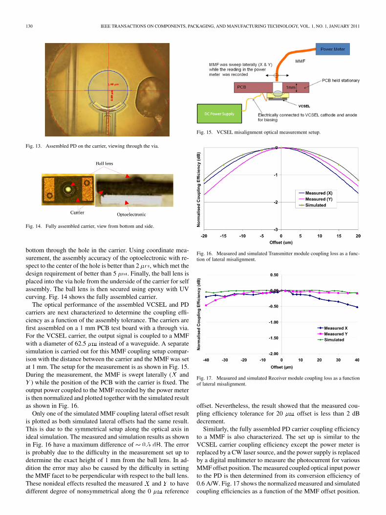
The optical performance of the assembled VCSEL and PDcarriers are next characterized to determine the coupling effi-ciency as a function of the assembly tolerance. The carriers arefirst assembled on a 1 mm PCB test board with a through via.For the VCSEL carrier, the output signal is coupled to a MMFwith a diameter of 62.5 instead of a waveguide. A separatesimulation is carried out for this MMF coupling setup compar-ison with the distance between the carrier and the MMF was setat 1 mm. The setup for the measurement is as shown in Fig. 15.During the measurement, the MMF is swept laterally ( and
) while the position of the PCB with the carrier is fixed. Theoutput power coupled to the MMF recorded by the power meteris then normalized and plotted together with the simulated resultas shown in Fig. 16.
Only one of the simulated MMF coupling lateral offset resultis plotted as both simulated lateral offsets had the same result.This is due to the symmetrical setup along the optical axis inideal simulation. The measured and simulation results as shownin Fig. 16 have a maximum difference of . The erroris probably due to the difficulty in the measurement set up todetermine the exact height of 1 mm from the ball lens. In ad-dition the error may also be caused by the difficulty in settingthe MMF facet to be perpendicular with respect to the ball lens.These nonideal effects resulted the measured and to havedifferent degree of nonsymmetrical along the 0 reference
Fig. 15. VCSEL misalignment optical measurement setup.
Fig. 16. Measured and simulated Transmitter module coupling loss as a func-tion of lateral misalignment.
Fig. 17. Measured and simulated Receiver module coupling loss as a functionof lateral misalignment.
offset. Nevertheless, the result showed that the measured cou-pling efficiency tolerance for 20 offset is less than 2 dBdecrement.
Similarly, the fully assembled PD carrier coupling efficiencyto a MMF is also characterized. The set up is similar to theVCSEL carrier coupling efficiency except the power meter isreplaced by a CW laser source, and the power supply is replacedby a digital multimeter to measure the photocurrent for variousMMF offset position. The measured coupled optical input powerto the PD is then determined from its conversion efficiency of0.6 A/W. Fig. 17 shows the normalized measured and simulatedcoupling efficiencies as a function of the MMF offset position.

GUAN et al.: INTEGRATED OPTICAL CARRIER FOR OPTICAL/ELECTRICAL INTERCONNECT 131
Although this measurement also suffered from nonideal setup,the difference between the measured and simulated results areless significant, approximately 0.5 dB. This is because the PDhas a large active area which is much smaller than the focusbeam spot of the ball lens. The measured result showed that thecoupling efficiency has an offset tolerance of for decre-ment of 0.5 dB. The optical measurement and simulation resultsfor the VCSEL and PD integrated optical carriers are closelymatched. This shows that the designs of these integrated opticalcarriers are viable and can enhance the assembly misalignmenttolerance.
V. CONCLUSION
The proposed optical integrated carrier can be used for allcommercial available flip chip design surface or surface illumi-nated optoelectronic components, i.e., VCSEL and standard PD,to enhance their coupling efficiency. The optical integrated car-rier can also be designed for multiple channels using array opto-electronic components. Although the substrate used for this car-rier is ceramic, silicon is preferred. This is because of the muchhigher fabrication accuracy as it uses semiconductor process andmicromachining technology. In addition, the recent advance-ment in the through silicon via process can be used to providefine pitch electrical interconnections that is required for inte-grating multiple channel, additional high-speed electrical ICsand circuit on the carrier. This becomes a system-in-packagewith optical function integration.
ACKNOWLEDGMENT
The authors would like to thank the following peoples fortheir support and valuable advice throughout this project.N. Zheng, Y. Chieng, and D. Harrison from Finisar Singapore,F. Yu, C. Xi, and Z. Xixi from Huawei Technologies, H. Kokiand K. Masahiko from Hitachi Cable.
REFERENCES
[1] M. Schneider, T. Kuhner, T. Alajoki, A. Tanskanen, and M. Karppinen,“Multi channel in-plane and out-of-plane couplers for optical printedcircuit boards and optical backplanes,” in Proc. 59th ECTC, May 2009,pp. 1942–1947.
[2] M. Immonen, M. Karppinen, and J. K. Kivilahti, “Fabrication andcharacterization of polymer optical waveguides with integrated micromirrors for three-dimensional board-level optical interconnects,” IEEETrans. Electron. Packag. Manuf., vol. 28, no. 4, pp. 304–311, Oct.2005.
[3] T. G. Lim, P. V. Ramana, B. S. P. Lee, T. Shioda, H. Kuruveettil, L.Jing, K. Suzuki, K. Fujita, K. Yamada, D. Pinjala, and J. L. H. Shing,“Demonstration of direct coupled optical/electrical circuit board,”IEEE Trans. Adv. Packag., vol. 32, no. 2, pp. 509–516, May 2009.
[4] F. E. Doany, C. L. Schow, C. W. Baks, D. M. Kuchta, P. Pepeljugoski,L. Schares, R. Budd, F. Libsch, R. Dangel, F. Horst, B. J. Offrein, and J.A. Kash, “160 Gb/s bidirectional polymer-waveguide board-level op-tical interconnects using CMOS-based transceivers,” IEEE Trans. Adv.Packag., vol. 32, no. 2, pp. 345–359, May 2009.
[5] A. K. Nallani, T. Chen, D. J. Hayes, W.-S. Che, and J.-B. Lee, “Amethod for improved VCSEL packaging using MEMS and ink-jet tech-nologies,” J. Lightwave Technol., vol. 24, pp. 1504–1512, Mar. 2006.
[6] M. Karppinen et al., “Parallel optical interconnect between ceramicBGA packages on FR4 board using embedded waveguides and passiveoptical alignments,” in Proc. 56th ECTC, 2006, pp. 799–805.
[7] Y.-H. Huang, C.-C. Yang, T.-C. Peng, M.-C. Wu, C.-L. Ho, and W.-J.Ho, “Alignment tolerance enlargement of ahigh-speed photodiode bya self-positioned microball lens,” Photon. Technol. Lett., vol. 18, pp.112–114, Jan. 2006.
[8] S. H. Hwang, J. W. Lim, and B. S. Rho, “120 Gb/s-level VCSEL arrayoptical subassembly using passive alignment technique,” Proc. 58thECTC 200, pp. 1620–1624, May 2008.
[9] D. A. B. Miller, “Rationale and challenges for optical interconnects toelectronic chips,” Proc. IEEE, vol. 88, pp. 728–749, Jun. 2000.
[10] M. Forbes, J. Gourlay, and M. Desmulliez, “Optically interconnectedelectronic chips: A tutorial and review of the technology,” Electron.Commun. Eng. J., vol. 13, pp. 221–232, Oct. 2001.
[11] Z. Toffano, A. Gholami, M. Fez, A. Destrez, and M. Marec, “VCSELshort reach communications: Behavioural modelling of high speed op-toelectronic modules,” in Proc. 4th Int. Conf. Numerical SimulationOptoelectronic Devices, Aug. 2004, pp. 49–50.
Lim Teck Guan received the Diploma in electronicsand communication engineering, and the AdvancedDiploma in telecommunications from SingaporePolytechnic, in 1992 and 1998, respectively, andthe B.Eng degree. (first class honours) in electronicand electrical engineering and the Ph.D. degree inmicrowave photonics engineering from University ofSurrey, Surrey, U.K., in 2001 and 2005, respectively.
From 1992 to 1998, he served as an Avionics Spe-cialist in Republic of Singapore Air Force, specializein electronic warfare. Currently, he is a Senior Re-
search Engineer in Microsystems, Modules and Components Laboratory of In-stitute of Microelectronics. He is responsible for the optical and electrical designfor the packaging and is the group leader for the Electrical Design and Simula-tion Team. His research interests include microwave and millimeter wave inte-grated circuit.
Dr. Guan was awarded The Lord Lloyd of Kilgerran Memorial Prize, IET,U.K. in 2002 for his postgraduate study.
Khoo Yee Mong received the B.S. degrees inelectrical engineering from the National Universityof Singapore, in 2005.
His current research interests includes RF pas-sives, system in package, and high-frequencyde-embedding.
Joey Chai Yi Yoon was born in Singapore, in 1981.She received the degree in electrical and electronicsengineering from National Technological University,Singapore, in 2005. She is currently working towardthe M.Sc. degree in electrical engineering in theDepartment of Electrical and Computer Engineering,National University of Singapore.
She worked in Institute of Microelectronics, Sin-gapore for three years from 2006, as a Research Of-ficer, and her work involved design and characteriza-tion of optical transceivers and optical interconnects.
She is currently working in DSO National Laboratories as a Research and Devel-opment Engineer and her research focus is on microwave photonics. She has twopublications in international conference proceedings and coauthored in journalpapers.
Calivn Teo Wei Liang, photograph and biography not available at the time ofpublication.

132 IEEE TRANSACTIONS ON COMPONENTS, PACKAGING, AND MANUFACTURING TECHNOLOGY, VOL. 1, NO. 1, JANUARY 2011
Germaine Hoe Yen Yi received the B.S. degree inmechanical engineering from Stanford University,Stanford, CA, in 2007.
She has been with the Institute of Microelec-tronics (IME), Singapore since 2008. Currently, sheis a Research Officer at the Microsystems, Modulesand Components Laboratory, IME, Singapore. Herresearch interests cover computational thermal mod-eling and analysis, experimental thermal packagecharacterization, two-phase cooling with mixturesand bioMEMs sensors.
Yap Guan Jie, photograph and biography not available at the time of publica-tion.
Pamidighantam V. Ramana received the M.S. de-gree in applied optics from the National Institute ofTechnology, Warangal, India, in 1984.
He has been a Member of Technical Staff (MTS) atInstitute of Microelectronics (IME), Singapore, sinceNovember 2001. He has over 23 years of experiencein opto-electronics research and development in re-search institutes and multinational companies. His re-search interests include optical interconnects, opticalimaging, illumination optics, and optical componentpackaging. Prior to joining IME in 2001, he worked
in the R&D Departments of Philips Optical Storage and Agilent Technologies.Before coming to Singapore, he was working in a military research institute withthe Ministry of Defence, Government of India, on imaging and nonimaging op-tical guidance for missile systems. He has coauthored more than 50 researchpublications and has 10 invention disclosures in optics related products.
Tan Chee Wei, photograph and biography not available at the time of publica-tion.
Damaruganath Pinjala, photograph and biography not available at the time ofpublication.