Interconnect intellectual property for Network-on-Chip (NoC
15
Interconnect intellectual property for Network-on-Chip (NoC) Jian Liu * , Li-Rong Zheng 1 , Hannu Tenhunen 2 Laboratory of Electronics and Computer Systems (LECS), Royal Institute of Technology (KTH), Institute of Microelectronics and Information Technology (IMIT), Electrum 229, SE-164-40 Kista, Stockholm, Sweden Abstract As technology scales down, the interconnect for on-chip global communication becomes the delay bottleneck. In order to provide well-controlled global wire delay and efficient global communication, a Network-on-Chip (NoC) architecture was proposed by different authors [Route packets, not wires: on-chip interconnection networks, in: Design Automation Conference, 2001, Proceedings, p. 684; Network on chip: an architecture for billion transistor era, in: Proceeding of the IEEE NorChip Conference, November 2000; Network on chip, in: Proceedings of the Conference Radio vetenskap och Kommunication, Stockholm, June 2002]. NoC uses Interconnect Intellectual Property (IIP) to connect different resources. Within an IIP, the switch has the central function. Depending on the network core of the NoC, the switch will have different architectures and implementations. This paper first briefly introduces the concept of NoC. It then studies NoC from an interconnect point of view and makes projections on future NoC parameters. At last, the IIP and its components are described, the switch is studied in more detail and a time–space–time (TST) switch designed for a circuit switched time-division multiplexing (TDM) NoC is proposed. This switch supports multicast traffic and is implemented with random access memory at the input and output. The input and output are then con- nected by a fully connected interconnect network. Ó 2003 Elsevier B.V. All rights reserved. 1. Introduction Interconnect has been the major design con- straint in deep sub-micron (DSM) circuits. The downscaled wire size, increased aspect ratio, combined with higher signal speed cause many signal integrity challenges and timing closure problems. Traditionally, these issues are tackled mainly from an electrical design point of view. Recent studies show that the problem also can be coped with interconnect-centric system architec- tures [2,7,8]. One such emerging architecture is the Network-on-Chip (NoC). The NoC architecture is a data packet based communication network on a single chip. It scales from a few dozens to several hundreds resources. A resource may be a processor core, a DSP core, an FPGA block, or any other intellectual property (IP) block. The resources are connected by Interconnect IPs. The structured network wiring gives well-controlled electrical pa- rameters and enables reusing of building blocks. Clearly, any topology that fully connects the * Corresponding author. Tel.: +46-8-790-4197; fax: +46-8- 751-1793. E-mail addresses: [email protected] (J. Liu), lrzh- [email protected] (L.-R. Zheng), [email protected] (H. Tenh- unen). 1 Tel.: +46-8-790-4104. 2 Tel.: +46-8-790-4119. 1383-7621/$ - see front matter Ó 2003 Elsevier B.V. All rights reserved. doi:10.1016/j.sysarc.2003.07.003 Journal of Systems Architecture 50 (2004) 65–79 www.elsevier.com/locate/sysarc
Transcript of Interconnect intellectual property for Network-on-Chip (NoC

Journal of Systems Architecture 50 (2004) 65–79
www.elsevier.com/locate/sysarc
Interconnect intellectual property for Network-on-Chip (NoC)
Jian Liu *, Li-Rong Zheng 1, Hannu Tenhunen 2
Laboratory of Electronics and Computer Systems (LECS), Royal Institute of Technology (KTH), Institute of Microelectronics
and Information Technology (IMIT), Electrum 229, SE-164-40 Kista, Stockholm, Sweden
Abstract
As technology scales down, the interconnect for on-chip global communication becomes the delay bottleneck. In
order to provide well-controlled global wire delay and efficient global communication, a Network-on-Chip (NoC)
architecture was proposed by different authors [Route packets, not wires: on-chip interconnection networks, in: Design
Automation Conference, 2001, Proceedings, p. 684; Network on chip: an architecture for billion transistor era, in:
Proceeding of the IEEE NorChip Conference, November 2000; Network on chip, in: Proceedings of the Conference
Radio vetenskap och Kommunication, Stockholm, June 2002]. NoC uses Interconnect Intellectual Property (IIP) to
connect different resources. Within an IIP, the switch has the central function. Depending on the network core of the
NoC, the switch will have different architectures and implementations. This paper first briefly introduces the concept of
NoC. It then studies NoC from an interconnect point of view and makes projections on future NoC parameters. At last,
the IIP and its components are described, the switch is studied in more detail and a time–space–time (TST) switch
designed for a circuit switched time-division multiplexing (TDM) NoC is proposed. This switch supports multicast
traffic and is implemented with random access memory at the input and output. The input and output are then con-
nected by a fully connected interconnect network.
� 2003 Elsevier B.V. All rights reserved.
1. Introduction
Interconnect has been the major design con-
straint in deep sub-micron (DSM) circuits. The
downscaled wire size, increased aspect ratio,
combined with higher signal speed cause many
signal integrity challenges and timing closure
* Corresponding author. Tel.: +46-8-790-4197; fax: +46-8-
751-1793.
E-mail addresses: [email protected] (J. Liu), lrzh-
[email protected] (L.-R. Zheng), [email protected] (H. Tenh-
unen).1 Tel.: +46-8-790-4104.2 Tel.: +46-8-790-4119.
1383-7621/$ - see front matter � 2003 Elsevier B.V. All rights reserv
doi:10.1016/j.sysarc.2003.07.003
problems. Traditionally, these issues are tackled
mainly from an electrical design point of view.
Recent studies show that the problem also can be
coped with interconnect-centric system architec-
tures [2,7,8]. One such emerging architecture is the
Network-on-Chip (NoC). The NoC architecture is
a data packet based communication network on a
single chip. It scales from a few dozens to severalhundreds resources. A resource may be a processor
core, a DSP core, an FPGA block, or any other
intellectual property (IP) block. The resources are
connected by Interconnect IPs. The structured
network wiring gives well-controlled electrical pa-
rameters and enables reusing of building blocks.
Clearly, any topology that fully connects the
ed.

66 J. Liu et al. / Journal of Systems Architecture 50 (2004) 65–79
resources can be used for the network. However, a
two-dimensional mesh topology turns out to be
simple and effective [2,11]. Therefore, the following
study will be based on this specific topology.
Conceptually, the NoC resources are connected
by IIPs to form a two-dimensional mesh as shownin Fig. 1. Each IIP is connected to its four closest
neighbors and to its corresponding resource. The
data from one resource is first passed to the IIP
attached to the resource. The IIP then packets the
data and routes the data packets onto the appro-
priate link, see also Section 4 for more detail.
As the NoC is targeted to future deep sub-mi-
cron (DSM) and nanometer technologies, the fol-lowing questions related to physical constraints
are interesting: what is the appropriate size of each
synchronous resource; how many resources can be
integrated in one chip in future technologies and
how to get an optimal data bandwidth with limited
wire resource. In Section 2, we use empirical rules
to derive the gate delays for future DSM tech-
nologies, which is followed by an estimation of themaximum clock frequency and the corresponding
resource size. In Section 3, the inter-resource delay
is studied and expressions for maximum inter-re-
source bandwidth are derived.
The NoC is a typical interconnect-centric ar-
chitecture, which means that the wire planning is
the first design step. In this early planning stage,
detailed system parameters for the wires are oftenunknown, making it impractical to consider lay-
out-related properties such as 3D multilayer in-
terconnections. Therefore, a simpler wire model is
used in the interconnect analysis below. When the
planning is done and various requirements on the
IIP
R
IIP
IIP IIP
R
IIP
IIP
R
R R R
Fig. 1. The 2D-mesh NoC backbone with resources (R) and
interconnect IPs (IIP).
wires, such as delay and noise level, are determined,
a dynamic interconnect model can be used to
generate a wire structure meeting these require-
ments in later design phases. One dynamic inter-
connect model using 3D capacitance, resistance
and inductance is described in [15]. Similar CADtools like Magma�s FixedTiming (www.magma-
da.com) are also emerging commercially.
At a high level, the NoC architecture and IIPs
must provide transparent and efficient inter-re-
source communication. In Section 4, the different
layers in NoC and the main IIP modules are de-
scribed. A case study of a time–space–time (TST)
switch designed for circuit switched time-divisionmultiplexing (TDM) NoC is carried out in Section
5. This switch supports multicast traffic and is
scheduled dynamically. A scheduling algorithm is
analyzed. The algorithm schedules the mapping
between the input and output in such a way that
the required memory bandwidth is reduced.
2. Global wire planning for NoC
The performance of interconnections is a major
concern in scaled technologies. Under scaling, the
gate delay decreases. However, the global wires do
not scale in length since they communicate signals
across the chip. For these wires, the delay per unit
length can be kept constant if optimal repeatersare used [1,6]. In the following study, we assume
that global wires are reserved for global commu-
nications and semi-global wires/local wires are
used within a resource. To estimate the size of each
resource, we first find the typical gate delay, which
determines the maximum clock rate using an em-
pirical approach. The maximum size of the re-
source can then be estimated under assumptionthat in a synchronous resource, a signal must
travel from one corner of the resource to the op-
posite within one clock cycle.
2.1. Technology scaling and gate delay
Since four is the typical average gate connec-
tivity, ‘‘fan-out-of-four inverter delay’’, or simplyFO4 is a reasonable parameter to be used for
measuring gate delays. As the name suggests, an

L1 cycle
Fig. 2. The worst-case delay in a resource.
J. Liu et al. / Journal of Systems Architecture 50 (2004) 65–79 67
FO4 is the delay through an inverter driving four
identical copies. In a 0.18 lm technology, an FO4
is about 90 ps under worst-case environmental
conditions (high temperature and low Vdd). Ho
et al. [6] pointed out that, historically, gates have
scaled linearly with technology, and an accuratemodel of recent FO4 delays has been 360Lgate ps at
typical and 500Lgate ps under worst-case environ-
mental conditions. After studying today�s existingnanometer scale devices, he also predicts that this
trend will continue for future generations of
transistors, which means 500Lgate ps is a lower limit
for future FO4 delays. This model of gate delay
will be used later when estimating clock cycle timeand comparing with wiring delays.
2.2. Clock cycle analysis
A resource in a NoC can run at different speed.
In [6], Ho showed that extrapolating historical
data would lead to 6–8 FO4s per clock cycle in the
near future. However, such fast-cycling machinespose many difficulties such as skew and long rise
and fall time (compared to clock cycle). With these
difficulties in consideration, a clock cycle of 20
FO4s is projected for a cost-performance NoC
resource and 10 FO4s for a high-performance one.
Thus, with 0.05 lm technology, the clock cycle
becomes 20 · 500 · 0.05¼ 500 ps for a cost-per-
formance NoC resource, giving a clock frequencyof 2 GHz. Table 1 shows projected clock fre-
quencies for some different technologies.
2.3. NoC resource size estimation
Knowing the projected clock cycle, the maxi-
mum size of a synchronous NoC resource is lim-
Table 1
Projected clock frequencies for NoC resources under worse-case
FO4 delays
0.18
lm0.13
lm0.10
lm0.07
lm0.05
lm
Cost performance
(GHz)
0.56 0.77 1.0 1.4 2.0
High performance
(GHz)
1.1 1.5 2.0 2.9 4.0
ited by the wiring delays since the clock signal
must be able to traverse 2 resource edges within aclock cycle (assuming the resource is quadratic) in
the worst case, see Fig. 2.
The wiring delay of a distributed RC line can be
modeled as
Twire ¼ 0:4rcl2
Here Twire is the wiring delay, l is the wire length, ris the resistance per unit length and c is the ca-
pacitance per unit length. This is a very good ap-
proximation and is reported to be accurate to
within 4% for a very wide range of r and c [12].Knowing the clock cycle time and RC delay model,
the maximum resource size satisfies
max wiring delay < clock cycle
) 0:4rcð2LÞ2 < clock cycle
Here, L is the maximum resource edge length. The
clock cycle estimation is described in previous
section and qualified predictions on wire resistance
and capacitance for future technologies are avail-
able in a number of different papers.The RC-model given above shows that the
wiring delay grows quadratically with wire length.
To reduce the delay for semi-global and global
wires, a long line can be broken into shorter sec-
tions, with a repeater (an inverter) driving each
section, see Fig. 3. This makes the total wire delay
h h h h
k321 . . .
. . .
l
Fig. 3. A long wire with k repeaters, each with a size of h times
the minimum sized inverter.

68 J. Liu et al. / Journal of Systems Architecture 50 (2004) 65–79
equal to the number of repeated sections multi-
plied by the individual section delay
Ttotal ¼ kðTdrv þ 0:4rcðl=kÞ2ÞNow, a first order model of the driver (repeater),
with lumped output resistance and input capaci-
tance, gives the driver delay as [12]:
Tdrv ¼ 0:7Rh
hC0
�þ hCg þ c
lk
�þ 0:7r
lkhCg
Here, R is the resistance of a minimum sized in-
verter, C0 and Cg are diffusion and gate capaci-tances of a minimum sized inverter and r and c arewire resistance and capacitance per unit length.
The expression above for the total delay can be
minimized and the minimum delay per unit length
can be shown to be 2:13ffiffiffiffiffiffiffiffiffiffiffiffiffiffircFO1
pps/mm [6,13].
Here, FO1 stands for fan-out-of-one delay and
1FO4� 3FO1. The time for a signal to traverse 2
resource edge lengths should be less than a clockcycle, suggesting the inequality 4:26L
ffiffiffiffiffiffiffiffiffiffiffiffiffiffircFO1
p<
1clock cycle. Using the predicted future semi-glo-
bal wire (with a width of approximately 3.5 times
the minimum feature size) parameters provided in
[13], as shown in Table 2, the maximum synchro-
nous resource size and the number of resources on
a single chip are calculated and listed in Table 3.
The resistance and capacitance used to calculateTable 3 are for semi-global wire, since the semi-
global wire is normally used within a resource.
Routing with global wires within a resource would
Table 2
Wire parameters for different technologies
Wire type Parameter 0.18 lm 0.13
Semi-global r (X/mm) 107 185
c (fF/mm) 331 268
Table 3
Maximum resource size and number of resources on a single chip, w
Technology 0.18 lmChip length (mm) 20
High performance Max resource size 6.5
No. of resources 9
Cost performance Max resource size 13
No. of resources 2
allow larger resource size, since global wires, in
general, have lower resistance and therefore also
smaller delay per unit length than semi-global
wires. From the table, we have that the maximum
size of a synchronous high performance resource is
1.5 mm using 0.05 lm technology. For a costperformance resource with a cycle time of 20
FO4s, twice as long as the high performance re-
source cycle time, the maximum resource size is
also twice as large.
It should be noted that the analysis made above
is valid for single wires. Crosstalk effects are not
taken into consideration. If many wires are in
parallel and switch simultaneously, the delay willbe higher for unfavorable switch patterns, requir-
ing smaller resource size. Therefore, the derived
maximum resource size above should be seen as an
upper bound.
3. Inter-resource bandwidth
3.1. Inter-resource delay
The inter-resource communication link will
most likely consist of a large number of parallel
wires, with uniform coupling over most of the wire
length. For such closely coupled parallel wire
structures, the crosstalk effects are considerable
and cannot be neglected. Hence, the single wiremodel used in previous section is not valid here.
lm 0.10 lm 0.07 lm 0.05 lm
317 611 1196
208 170 155
ith different technologies
0.13 lm 0.10 lm 0.07 lm 0.05 lm21 23 25 28
4.7 3.5 2.4 1.5
20 42 112 350
9.3 7.1 4.7 3.0
5 10 28 87

CcCs
CsVictim Line
Aggressor Line
CsAggressor Line
Cc
R
R
R
Fig. 4. Distributed RC lines with uniform coupling.
J. Liu et al. / Journal of Systems Architecture 50 (2004) 65–79 69
Instead, the model shown in Fig. 4 is used. Each
wire is modeled as a distributed RC line with total
resistance R, total self-capacitance Cs, and total
coupling capacitance Cc uniformly distributed overthe whole line.
The effect of crosstalk on the delay depends on
the switching pattern of the aggressor (adjacent)
lines [1,12]. In Fig. 4, suppose that the victim line
in the middle switches up from zero to one, Pam-
unuwa shows in [12] that the switching pattern
that gives rise to the worst case delay on the victim
line is when the two aggressor lines switch downfrom one to zero (almost) simultaneously. The
worst-case delay is then given by
t0:5 ¼ 0:7RdrvðCs þ 4:4Cc þ CdrvÞþ Rð0:4Cs þ 1:5Cc þ 0:7CdrvÞ
Here, t0:5 is the delay for step response to reach
50% point, Rdrv is the driver (minimum sized in-
verter) output resistance and Cdrv is the driver ca-
pacitance. Similar to the single wire case, the
second term in this expression grows quadraticallywith the wire length. Inserting repeaters reduces
the total wire delay. As shown in Fig. 5, a long
wire is broken into k sections, with an h-sized re-
peater driving each section. For each section, the
driver has a lumped resistance of Rdrv=h and ca-
pacitance of h � Cdrv, the wire has a distributed re-
sistance of R=k and self-capacitance Cs=k, the
Cs/k
2Cc/kRdrv/h
R/k1 2
Vin2Cc/k
R/k
hCdrvCs/k
Rdrv/h
Fig. 5. Insertion of repeaters in a
mutual capacitance becomes Cc=k between two
adjacent lines.
Applying the formula for worst-case delay for
each section, the total wire delay becomes
t0:5 ¼ k 0:7Rdrv
hCs
k
��þ hCdrv þ 4:4
Cc
k
�
þ Rk
0:4Cs
k
�þ 1:5
Cc
kþ 0:7hCdrv
��
To obtain the optimal k and h value, the partial
derivatives are equaled to zero, giving [12]
ot0:5ok
¼ 0 ) kopt ¼
ffiffiffiffiffiffiffiffiffiffiffiffiffiffiffiffiffiffiffiffiffiffiffiffiffiffiffiffiffiffiffiffiffiffi0:4RCs þ 1:5RCc
0:7RdrvCdrv
s
ot0:5oh
¼ 0 ) hopt ¼
ffiffiffiffiffiffiffiffiffiffiffiffiffiffiffiffiffiffiffiffiffiffiffiffiffiffiffiffiffiffiffiffiffiffiffiffiffiffiffiffiffiffiffi0:7RdrvCs þ 3:1RdrvCc
0:7RCdrv
s
Now, the optimal value of k must be a positiveinteger. Using the minimum sized inverter resis-
tance and capacitance from [10], as shown in Table
4, the optimal k and h values are calculated and
listed in Table 5. If the optimal k is not an integer,
both of the two closest integers are used and cor-
responding delays are compared to each other in
order to find the smallest delay.
From Table 5, we see that the optimal size ofthe repeaters is large and the number of sections
does not seem to be very significant for the delay.
hCdrv
3 kCs/k
Rdrv/h 2Cc/k
R/k
uniformly coupled RC line.

Table 4
Resistance and capacitance of minimum sized inverter for dif-
ferent technologies
0.18
lm0.13
lm0.10
lm0.07
lm0.05
lm
Inverter
resistance
(X)
9020 10,560 11,370 13,710 15,080
Inverter
capaci-
tance (fF)
1.795 1.267 0.996 0.709 0.532
0 0.5 1 1.5 2 2.5 3 3.5 4100
101
Data Rate Per Wire (Gb/s)
Crit
ical
Dis
tanc
e (/
mm
)
from 0.18um to 0.05um tech.with repeaters
from 0.18um to 0.05um tech.without repeaterts
Fig. 6. Maximum length of a global wire for different band-
widths and technologies, with and without repeaters.
70 J. Liu et al. / Journal of Systems Architecture 50 (2004) 65–79
The increased number of repeaters only gives
marginal improvement in delay. This means that
the trade-off between the number of repeaters and
the delay should be considered. Also, since the
distance between two adjacent switches is one re-
source edge (neglecting the overhead areas forswitches), it might be preferable not to choose the
largest possible resource size. By doing so, the area
consuming and power hungry repeaters can be
avoided. From this point of view, the resource size
should be chosen such that k ¼ 1 gives the mini-
mum delay. Comparing Tables 3 and 5, we can
clearly see that the largest possible resource sizes
require repeaters to reach the minimum delay.
3.2. Inter-resource bandwidth estimation
The wire delay limits the inter-resource band-
width and distance. To see how these quantities
are related, we first assume that a good signal has
duration of at least 3tr, where tr is the time for a
rising signal to rise from 10% to 90% of its finalvalue. Usually, for RC delays, 0–50% time
t0:5 ¼ 0:69s and tr ¼ 2:2s [14], where s is the RCtime constant. Thus, the bandwidth of a single
Table 5
Optimal size of the repeaters, h, optimal number of sections, k, close
Technology 0.18 lm 0.13 lm
Optimal h 322 296
Optimal k (1/mm) 0.99 1.30
Integer k (1/mm) 1 1
Total delay (ps/mm) 65.5 73.2
Integer k (1/mm) 1 2
Total delay (ps/mm) 65.5 71.3
wire is limited by 1=9t0:5. Fig. 6 shows the allowed
maximum length of a global wire at different
bandwidths, with and without repeaters. Clearly,
for same technology and wire length, wires with
repeaters can have higher bandwidth due to their
low propagation delay. For an inter-resource dis-
tance of 1.5 mm with 0.05 lm technology (as-suming that the resources are close to each other
and the inter-resource distance is therefore equal
to the resource size), the bandwidth between two
adjacent resources is estimated to 0.6 Gbps per
global wire without repeaters.
3.3. Variable wire width and spacing
In the previous Section, fixed predictions are
used as future wire parameters. In a real process,
the wire width and pitch is typically limited by the
minimum feature size of the technology. As long
st integer values of k and corresponding delay per unit length
0.10 lm 0.07 lm 0.05 lm
226 187 154
1.66 2.28 3.33
1 2 3
83.7 91.8 110
2 3 4
76.0 90.1 108

R
NI
S
MUX
R
NI
S
MUX
InterconnectIP
Fig. 7. The interconnect IP modules. R¼ resource, NI¼Net-
work Interface and S¼ switch.
J. Liu et al. / Journal of Systems Architecture 50 (2004) 65–79 71
as this condition is fulfilled, the wire width and
spacing can be varied freely to maximize the inter-
resource bandwidth. For a given total width of the
wires, the choice of wire width and pitch decides
the total bandwidth. Clearly, wider wires and lar-
ger spacing give higher bandwidth per conductor.But the number of conductors allowed in the given
total width is also smaller.
Using simulations, Pamunuwa shows in [12] the
optimal wire width and spacing with different
constraints. For a total wire width of 15 lm, using
copper wires with technology dependent constant
b ¼ 1:65, minimum wire width w ¼ 0:1 lm, mini-
mum distance between two adjacent wires s ¼ 0:1lm, distance between the signal wires and ground
plane h ¼ 0:2 lm, wire thickness t ¼ 0:21 lm(giving an aspect ratio of 2.1), the optimal number
of wires is 19 if ideal drivers are assumed and no
repeaters are used. Using real inverters with out-
put impedance of a minimum sized inverter 7 kX,input capacitance of the same inverter 1 fF and
optimal repeater insertion, maximum number ofwires allowed (75) also gives the maximum total
bandwidth on 20 Gbps.
4. The interconnect IP
To make NoC meaningful and attractive to use,
the communication between resources needs to betransparent, the interface between a resource and
an IIP needs to be standardized and the IIPs must
provide efficient and reliable communication ser-
vices required from an application point of view.
Using layered communication architecture and
standardized IIPs can fulfill these requirements.
Similar to a computer network with layered com-
munication protocols, the NoC is a layered net-work. The lowest four layers: transport layer,
network layer, link layer and physical layer are a
part of the NoC backbone and reside outside of
the resources.
The different layers mentioned above are im-
plemented in different modules. These layers, to-
gether with the modules that implement them,
form the Interconnect Intellectual Property (IIP)as shown in Fig. 7. The IIP provides the services
inter-resource communication relies on.
4.1. The network interface and MUX unit
4.1.1. NI functionality
The Network Interface (NI) works in thetransport layer. It is responsible for assemble/re-
assemble messages from/to multiple packets. As
described in Section 3.3, the optimal number of
wires between two switches may vary depending
on technology parameters and different con-
straints. In Fig. 7, a bold arrow directly connected
to a switch denotes a link with the wire configu-
ration (number of wires, wire width etc.) thatmaximizes the inter-resource (switch) bandwidth.
Each link handles traffic in only one direction so
bi-directional communication requires two links.
Different resources may have different number of
input and output signals. The NI controls the
multiplexing/demultiplexing unit (MUX) to map
the input and output signals of the resources to/
from the switch-to-switch link. It should be notedthat the MUX-to-switch link width and switch-to-
switch link width are the same to reduce the
complexity of the switch.
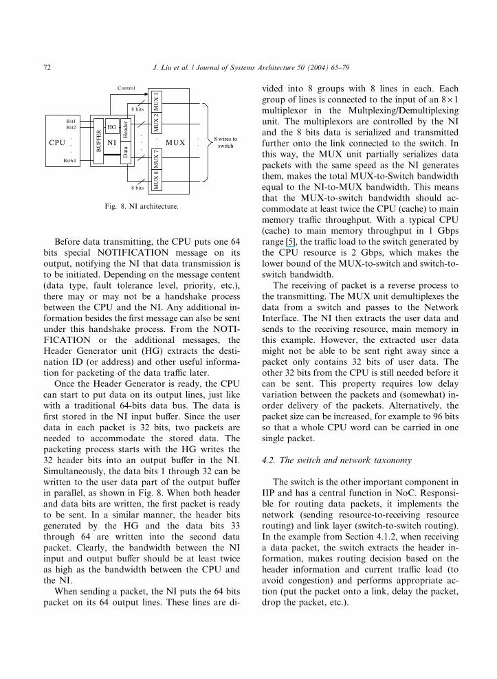
4.1.2. One NI example
One example on the mapping is shown in Fig. 8.
Here, the transmitting resource is a 64 bits CPU
and the link width between the switches is 8 wires.The receiving resource is a main memory (MM)
located somewhere else. Furthermore, a packet
size of 64 bits of which 32 are header bits is used in
this example. This packet structure is used just for
demonstration. It may be redefined as the com-
munication protocols are defined in more detail
and the traffic model more thoroughly analyzed.
.
.CPU
Bit1Bit2
Bit64
BU
FF
ER
.
.
.NI
MU
X2
MU
X7
MU
X1
MU
X8
Dat
aH
eade
r
.
.
.MUX
Control
8 bits
8 bits
.
.8 wires to
switch
HG
Fig. 8. NI architecture.
72 J. Liu et al. / Journal of Systems Architecture 50 (2004) 65–79
Before data transmitting, the CPU puts one 64
bits special NOTIFICATION message on its
output, notifying the NI that data transmission is
to be initiated. Depending on the message content
(data type, fault tolerance level, priority, etc.),
there may or may not be a handshake process
between the CPU and the NI. Any additional in-formation besides the first message can also be sent
under this handshake process. From the NOTI-
FICATION or the additional messages, the
Header Generator unit (HG) extracts the desti-
nation ID (or address) and other useful informa-
tion for packeting of the data traffic later.
Once the Header Generator is ready, the CPU
can start to put data on its output lines, just likewith a traditional 64-bits data bus. The data is
first stored in the NI input buffer. Since the user
data in each packet is 32 bits, two packets are
needed to accommodate the stored data. The
packeting process starts with the HG writes the
32 header bits into an output buffer in the NI.
Simultaneously, the data bits 1 through 32 can be
written to the user data part of the output bufferin parallel, as shown in Fig. 8. When both header
and data bits are written, the first packet is ready
to be sent. In a similar manner, the header bits
generated by the HG and the data bits 33
through 64 are written into the second data
packet. Clearly, the bandwidth between the NI
input and output buffer should be at least twice
as high as the bandwidth between the CPU andthe NI.
When sending a packet, the NI puts the 64 bits
packet on its 64 output lines. These lines are di-
vided into 8 groups with 8 lines in each. Each
group of lines is connected to the input of an 8 · 1multiplexor in the Multplexing/Demultiplexing
unit. The multiplexors are controlled by the NI
and the 8 bits data is serialized and transmitted
further onto the link connected to the switch. Inthis way, the MUX unit partially serializes data
packets with the same speed as the NI generates
them, makes the total MUX-to-Switch bandwidth
equal to the NI-to-MUX bandwidth. This means
that the MUX-to-switch bandwidth should ac-
commodate at least twice the CPU (cache) to main
memory traffic throughput. With a typical CPU
(cache) to main memory throughput in 1 Gbpsrange [5], the traffic load to the switch generated by
the CPU resource is 2 Gbps, which makes the
lower bound of the MUX-to-switch and switch-to-
switch bandwidth.
The receiving of packet is a reverse process to
the transmitting. The MUX unit demultiplexes the
data from a switch and passes to the Network
Interface. The NI then extracts the user data andsends to the receiving resource, main memory in
this example. However, the extracted user data
might not be able to be sent right away since a
packet only contains 32 bits of user data. The
other 32 bits from the CPU is still needed before it
can be sent. This property requires low delay
variation between the packets and (somewhat) in-
order delivery of the packets. Alternatively, thepacket size can be increased, for example to 96 bits
so that a whole CPU word can be carried in one
single packet.
4.2. The switch and network taxonomy
The switch is the other important component in
IIP and has a central function in NoC. Responsi-ble for routing data packets, it implements the
network (sending resource-to-receiving resource
routing) and link layer (switch-to-switch routing).
In the example from Section 4.1.2, when receiving
a data packet, the switch extracts the header in-
formation, makes routing decision based on the
header information and current traffic load (to
avoid congestion) and performs appropriate ac-tion (put the packet onto a link, delay the packet,
drop the packet, etc.).

J. Liu et al. / Journal of Systems Architecture 50 (2004) 65–79 73
So far, the NoC has been described as a com-
munication network based on data packets and the
high-level logic function of the switch is routing
the packets. For different network cores, different
approaches may be used for data packet routing.
In the following text, the traditional telecommu-nications network taxonomy (also apply on NoC),
which determines the low-level architecture and
implementation of the switch, will be studied.
As shown in Fig. 9, a traditional telecommu-
nications network either employs circuit or packet
switching. A link in a circuit switched network can
use either frequency-division multiplexing (FDM)
or time-division multiplexing (TDM) while packetswitched networks are either virtual circuit (VC)
networks or datagram networks [9]. This classifi-
cation can be generalized and apply on any net-
work core, including NoC.
4.2.1. Packet switching
Depending on the routing method, packet
switched networks are divided into virtual circuitnetworks and datagram networks. The virtual
circuit approach is connection-oriented and re-
sembles the circuit switching. Both packet swit-
ched VC network and circuit switched network are
suitable for uniform data traffic with long lifetime.
For other bursty traffic, the connection manage-
ment will tend to be computationally demanding
and occupy a large portion of the bandwidth. Theyalso require that the switches maintain the state
information, resulting in more complex switch
architecture and signaling scheme between
switches.
To reduce the switch complexity and therefore
also the area overhead, datagram switching can be
used. The datagram based switch is state- and
memoryless, each packet is treated independently,
Telecom Networks
Circuit-SwitchedNetworks
Packet-SwitchedNetworks
TDMFDMNetworkswith VCs
DatagramNetworks
Fig. 9. Telecommunication network taxonomy.
with no reference to preceding packets. This ap-
proach more easily adapts to changes in the net-
work such as congestion and dead links. However,
it does not guarantee that packets with same
source and destination will follow the same route.
Consequently, the delay of packets with samesource and destination may vary and packets may
also arrive out of order, requiring buffering ele-
ment at the receiving end. A datagram based
switch implementation is described in [11].
4.2.2. Circuit switching and Philips �thereal NoC
A circuit switched network requires a dedicated
end-to-end circuit (with a guaranteed constantbandwidth) between the transmitting and the
receiving end. As the ‘‘circuit’’ is an abstract con-
cept, most of the time, it is not a physical end-to-
end wire, but can span over many links. In a
telecommunications network, the circuit is typi-
cally implemented with either frequency-division
multiplexing or time-division multiplexing in each
link [9]. With FDM, the frequency spectrum of alink is shared among the connections across
the link. For obvious reasons, the FDM is not
suitable for NoC. For TDM on the other hand,
time is divided into frames of fixed duration, and
each frame is divided into a fixed number of time
slots as shown in Fig. 10. When the network es-
tablishes a connection (or circuit) across a TDM
link, the network dedicates a certain number oftime slots in every frame to the connection. These
slots are dedicated for the sole use of that con-
nection, with some time slots available for use (in
every frame) to transmit the connection�s data [9].
The Æthereal Network on Chip developed at
Philips Research is based on the time-division
multiplexed circuit switching approach described
above [4]. Here, the network provides two different
Time Slot
2
Frame
1 n
Fig. 10. Circuit realization with TDM.

FB
FBSMT
Input 0
Output 0
FB
FBSMT
Input 1
Output 1
FB
FBSMT
Input p-1
Output p-1
Fully Connected Interconnect
Fig. 11. Switch architecture for TDM circuit switched NoC
FB¼ frame buffer, SMT¼ slot map table.
74 J. Liu et al. / Journal of Systems Architecture 50 (2004) 65–79
kinds of services to support differentiated data
traffic: guaranteed throughput (GT) and best-offer
(BE) traffic. For the GT traffic, a connection needs
to be established before the actual transmission
can take place. When establishing a connection,
the switches reserve a number of time slots on eachlink along the path from the sending resource to
the receiving resource. This connection-oriented
service has many advantages. First, the congestion
control mechanism is built-in in the connection
establishing process, resulting in contention-free
traffic. Second, the time slots are fixed in each time
frame, meaning that the delay of a data packet
between two consecutive switches is bounded by atime frame. The total delay is then constant and
bounded by the number of hops between the two
ends multiplied with the time frame. At last, since
the delay is (approximately) constant for each GT
packet, the data packets will also be received in
order. The best-offer traffic is connectionless. It
uses unutilized time slots to transmit data packets.
More detailed information on the Æthereal NoCcan be found in [4].
5. A TST switch for circuit switched NoC
The circuit switched network is suitable for
uniform data traffic with long lifetime. Within a
communication channel, the data packets areguaranteed to arrive in order after a constant la-
tency. Also, multicast traffic can more easily be
supported. These features make circuit switching
scheme attractive for NoC. In this Section, we
describe a switch architecture designed for the
circuit switched NoC. It is essentially a traditional
time–space–time switch with the time slot inter-
changers (TSIs) at the input and output replacedby fast RAM memories. In order to reduce the
required bandwidth of the memories, the read and
write operations need to be scheduled evenly in
time.
5.1. Switch architecture
Fig. 11 shows the switch designed for circuitswitched NoC using TDM. It is assumed that the
switch has p inputs and outputs, where p is an
integer. Clearly, for the 2D mesh NoC topology
mentioned before, p ¼ 5. However, as the network
topology may vary, p may become large and that is
when the following study becomes meaningful in
practice. The frame buffers (FBs) associated to
each input and output are random access memo-ries each storing one frame (n data packets as
shown in Fig. 10) of data. There are two frame
buffers associated with each input. In a pipelined
fashion, one is written by the input and the other is
read by the interconnect and output. In the next
time frame, the first one (written by the input in
the previous frame) is read by the interconnect and
the second is written by the input. To reduce therequired memory bandwidth, the architecture in-
fers strictly controlled reading of the input frame
buffers by only having one memory read port per
input frame buffer. This implies that each memory
can be accessed only once each cycle. To achieve
this requirement, the read and write operations
need to be scheduled in such a way that the ac-
cesses are as evenly distributed in time as possible.There are also two frame buffers associated with
each output port. One is read by the output port
and the other is written with data in the next frame
by the interconnect. The interconnect itself is non-
blocking and supports multicast (for example a
crossbar).
The central component of the architecture is the
slot map tables (SMTs). Instead of using twostages of time slot interchangers and a crossbar
scheduler as in a traditional TST switch, the SMTs

ib is
1 1
0 2
0 0
(a) Output 0
ib is
0 1
2 2
1 2
(b) Output 1
ib is
2 1
1 0
2 0
(c) Output 2
Fig. 13. Equivalent SMTs with only two fields.
J. Liu et al. / Journal of Systems Architecture 50 (2004) 65–79 75
directly control the read and write operations to
the random access frame buffers. Similar to the
frame buffers, the number of SMTs for each out-
put is also two, one is currently in use to control
the read/write operations and the other is written
for use in the next time frame.
5.2. Slot map tables
To control the read/write operations, each entry
in an SMT consists of three fields, input buffer
number (ib), input slot number (is), and output
slot number (os). The output buffer number (ob) is
implicitly given since each SMT is associated withan output buffer. However, in the following text,
each entry in an SMT is represented by only two
fields, input number and input slot number. The
output slot number does not affect the scheduling,
since an output FB is written at most once in a
time cycle after scheduling. Therefore, the output
slot number is omitted in the representation to
simplify it. An example of the SMTs for a 3 · 3switch with frame length of 3 slots is shown in Fig.
12. The same SMTs with output slot number
omitted are shown in Fig. 13. It should be re-
membered that each entry actually consists of 3
fields although an entry is represented by two in
the following text. Only, with all these three fields
available, a data slot can be read from an input
buffer and written to appropriate correspondingoutput buffer(s).
A row in the SMTs corresponds to a time pe-
riod (cycle) long enough to perform a read/write
operation on the FBs. Its length depends on the
data length and the memory speed and does not
ib is os
1 1 1
0 2 2
0 0 0
(a) SMT for output buffer 0
ib is os
0 1 2
2 2 1
1 2 0
(b) SMT for output buffer 1
ib is os
2 1 0
1 0 1
2 0 2
(c) SMT for output buffer 2
Fig. 12. SMTs for a 3· 3 switch with frame length of 3 slots
ib¼ input buffer number, is¼ input slot number os¼ output
slot number.
have any connections to slot length in time frame.
For the example given in Fig. 12, the first row
means that following operations will take place in
the first writing time cycle: data at memory loca-tion 1 of input 1 is written to memory location 1 of
output 0, data at memory location 1 of input 0 is
written to memory location 2 of output 1, data at
memory location 1 of input 2 is written to memory
location 0 of output 2. It should be noted that the
three parallel read/write operations are from dif-
ferent inputs to different outputs. Due to possible
output contentions as a consequence of multicasttraffic described below, it may require more time
cycles than the number of time slots in a frame to
transfer a whole frame of data. Thus, the SMTs
may require more rows than the number of time
slots in a time frame. The following text will study
the exact number of rows required and try to find
scheduling algorithms to prevent output conten-
tion.
5.2.1. Unicast SMT scheduling
Unicast is a special case of multicast. With
unicast, each time slot from an input is mapped to
one single output and time slot. This means that
each entry is unique in a unicast SMT, i.e. there
are never two entries with same input number and
time slot number. Hence, an input number is onlyallowed to appear once in a given row across all
SMTs in order to avoid multiple read operations
of the same input. The representation of the
scheduling problem can now be simplified even
more by omitting the input time slot number in
each entry. This is justified because the input slot
number does not affect the scheduling since the
contention is for the whole input buffer of a giveninput port. For a given input buffer, it does not

ib
0
2
1
(b) Output 1
ib
2
1
2
(c) Output 2
ib
1
0
0
(a) Output 0
Fig. 14. Unicast representation of Figs. 12 and 13.
0
1
2
0
1
2
Inputs
Outputs
Time cycle 0
Time cycle 1
Time cycle 2
Fig. 15. Transformation of SMTs in Fig. 14 into minimal bi-
partite edge coloring.
76 J. Liu et al. / Journal of Systems Architecture 50 (2004) 65–79
matter which of its slots is read as long as it is read
only once in a time cycle. The same SMTs as
shown in Figs. 12 and 13 but with both output slot
number and input slot number omitted are shown
in Fig. 14.
Since each input number can appear at most n(frame length) times in the SMTs and there are pinputs, the scheduling problem can formally bestated as following:
Given n � p numbers, n 1s, n 2s. . . and n ps, allplaced in an n� p matrix (each column is an
SMT) such that each number occupies an entry in
the matrix. Empty entries are allowed to be in-
troduced in each of the p columns (these introduce
a NOP operation). The entries in same column can
be permuted freely (reorder the write operations toan output). By doing so, a new matrix with pcolumns and at least n rows can be built up, such
that each row contains only distinct numbers
(empty entries excluded). The task is to find the
minimum number of rows in the new matrix. This
minimum number of rows is also the required
length of the SMTs and the number of time cycles
needed to write a whole frame data from the inputto the output. Moreover, once the minimal num-
ber of rows is found, an efficient scheduling al-
gorithm is needed. The algorithm takes an
arbitrary n� p matrix described above and returns
a new matrix with each row containing distinct
numbers.
With this simplified representation, the sched-
uling problem can easily be transformed to thewell-studied minimal bipartite edge-coloring
problem in graph theory. A graph G ¼ ðV ;EÞ is
bipartite if the vertex set V can be partitioned into
two non-empty sets V1 and V2 in such a way that
every edge in E joins a vertex in V1 to a vertex in V2.
A coloring is to give each edge in E a color such
that no two edges sharing a vertex have same
color. The minimal bipartite edge coloring is to
find the minimum number of colors needed to
color a bipartite graph. Let each input and output
buffer be a vertex, a read/write operation betweenan input/output pair be an edge. The obtained
graph will be a bipartite graph. A minimal color-
ing of the graph will then correspond to an optimal
schedule, each color corresponds to a time cycle.
The requirement that no two edges with same
color share one vertex will guarantee no two read/
write operations in same time cycle.
Konig showed that every bipartite graph G hasa k-edge-coloring, where k is the maximum degree
of a node in G. In our unicast scheduling problem,
each input buffer is read and each output buffer is
written n times. Thus, a vertex in the transformed
problems will have a maximum degree of n. Thismeans n colors are enough to color the graph.
Consequently, an SMT length of n is enough (Fig.
15).There are many algorithms with different com-
putational complexity and memory consumption
proposed for the minimal bipartite edge-coloring
problem. The best running time known is
OðE logDÞ where E is the number of edges and Dthe maximum degree of the graph. In the trans-
formed scheduling problem, D ¼ n and E ¼ np.Thus there exists algorithm(s) with complexityOðnp log nÞ. Also, online scheduling algorithms of
complexity OðpÞ exist for each entry change. This
means that only OðpÞ operations are required to
reschedule after a channel change (channel estab-
lishment, channel termination and channel band-
width reallocation). We will not go into details of
all these algorithms here.

J. Liu et al. / Journal of Systems Architecture 50 (2004) 65–79 77
5.2.2. Multicast scheduling
With multicast, the data from one input mem-
ory location can be mapped to one or more dif-
ferent outputs. The number of outputs an input
memory location is mapped to is called the fan-outand is denoted by m. Clearly, the fan-out m is an
integer between 1 and p, the number of inputs and
outputs. Since a multicast consists a number of
reads from same memory location of same input,
the entries can, but do not have to be scheduled in
same row. Unlike the unicast case, the required
SMT length for multicast is not n, the number of
slots in a time frame due to output contentions.This is highlighted in Fig. 16. The red entries are
read operations from different memory locations
of same input and therefore have to be scheduled
in different rows. The green entries are multicast to
the outputs and can therefore be scheduled in same
row despite of the fact that they have the same
input number. It is similar for the blue entries.
They are from one and the same multicast andtherefore will not form contentions between
themselves. However, blue entries and green ones
are not allowed to be in same row as they are reads
from different memory locations of same input.
This means that three rows are not enough to
ib is os
1 0 2
0 0 0
0 1 1
ib is os
0 0 0
1 1 2
0 1 1
ib is os
0 0 0
0 1 1
1 2 2
Fig. 16. Multicast SMTs are longer than n, here n ¼ 3.
(a) SMT swith 3 in/out pairs and 3 times lots
Output 1 Output 2
ib is
1 1
3 2
2 3
ib is
1 1
2 2
3 3
ib is
2 1
2 2
3 3
Output 3
Fig. 17. SMTs and correspondin
schedule the mappings shown in Fig. 16 with
n ¼ 3.
Similar to the transformation for unicast case,
the multicast scheduling problem can easily be
transformed to edge coloring problem [3]. The
notations in graph theory simplify the problempresentation and therefore will be used in the fol-
lowing text. Let each input buffer be a sending
node and each output buffer be a receiving node.
Let also a read/write operation pair between an
input/output pair be an edge. The edges originat-
ing from one and the same multicast form a bun-
dle. Two coloring rules apply: (1) every pair of
edges from different bundles emanating from thesame sending node must be colored differently; and
(2) all incoming edges to each receiving node must
be colored differently. Then the minimal coloring
of the obtained graph will be the schedule with
each color corresponding to a time slot. It should
be noted that two edges with the same sending
node (in the same bundle) might, but do not have
to, have the same color. An example with threeinput/output pair using three time slots, and the
corresponding graph is shown in Fig. 17.
Without any limitations on n and p, Gonzalez
shows in [3] that the required number of colors is
n2 and finding the optimal coloring is NP-hard. At
a first glance, this seems to imply that multicast
scheduling is impossible to be carried out in
practice as n is likely to be large, typically severalhundred or even thousand and NP-hard problems
are impractical to solve when the input size grows.
However, the constructed graph Gonzalez makes
up to show the necessity of n2 rows requires a valueof p much larger than n. This is not the case in
R1 R2 R3
(b) Corresponding graph and a legal coloring
S2 S3S1
g a legally colored graph.

78 J. Liu et al. / Journal of Systems Architecture 50 (2004) 65–79
NoC application with p ¼ 5 for 2D mesh topol-
ogy. The NP-hard part can also be coped by using
approximative algorithms.
A coloring algorithm called q_color is provided
in [3]. It colors each bundle with at most q colors
using a total of qnþ m1=qðn� 1Þ colors. Here q is apositive integer parameter and m is the maximum
fan-out. With possible broadcast, m ¼ p. Given
the values of n and p, the optimal value of q (that
gives the least number of time slots required) can
easily be identified by differentiating the expression
with respect to q. The conditions for the optimal
value of q becomes
oðqnþ p1=qðn� 1ÞÞoq
¼ 0
) nþ ðn� 1Þðp1=q � ln p=q2Þ¼ 0
which can be solved numerically, under the con-
straint that q must be positive integer. The com-
plexity of the q_color algorithm can be shown to
be Oðn2pqÞ. For typical p values (up to 256), q is
less than 4. Here, we only want to show that fea-
sible scheduling algorithms supporting multicast
exit. More details about the q_color algorithm canbe found in [3].
6. Conclusions
In this paper, we studied the NoC system pa-
rameters and Interconnect Intellectual Property in
NoC. Predictions on future technology featuresize, clock speed in a synchronous resource, max-
imum NoC resource size, optimal global commu-
nication bandwidth and inter-resource distance,
are made. These quantities are closely related to
each other. The technology determines the gate
delay, which in turn determines the maximum
clock frequency. The maximum resource size can
then be derived from the obtained clock frequencyand the semi-global wire delay. Finally, the global
communication bandwidth is limited by the dis-
tance between resources and the global wire delay.
Providing estimations on these system parameters,
this paper provides a global wiring scheme using
the IIPs and can be used as a guideline for NoC
system architecture definition. This can be dem-
onstrated in a numerical example: for a NoC in 50
nm technology, the clock frequency is estimated to
be 4 GHz for a high-performance synchronous
resource with an edge length of 1.5 mm. With an
inter-resource distance of 1.5 mm, there is roomfor about 350 such resources on a single chip of
28 · 28 mm. The bandwidth between two adjacent
resources is estimated to be 0.6 Gbps per global
wire without using repeaters.
The IIPs connect different resources in NoC.
The main components in an IIP are the Network
Interface and the switch. As the number of wires
for optimal global communication bandwidthmight not be the same as the number of input/
output signal lines to/from a resource, the Net-
work Interface is needed. It also assembles/reas-
sembles data stream from/to a resource. The
switch has the function of routing the data packets
to their destination. For different types of under-
lying network cores, different switch architectures
and routing policies are possible. Simulationshows that a multiplexing/demultiplexing trans-
mission scheme of the IIP is feasible, independent
of the switch implementation.
A multicast-supporting time–space–time switch
is designed for time-division multiplexing NoC. It
is shown that feasible online scheduling algorithms
exit.
Future work evolves packet definition, reliablecommunication mechanism and different switch
architectures. For the TST switch architecture
proposed in this paper, simulations need to be
carried out to evaluate the performance of the
scheduling algorithms. Furthermore, applications
that fully utilize the services provided by NoC
need to be developed. At last, performance eval-
uation and estimation on area overhead of thepacket switched network are needed to compare it
to a more conventional bus structure and dedi-
cated wires.
Acknowledgements
This work is partly funded by the SOCWAREand COMPLAIN project. Productive discussions
with Dinesh Pamunuwa and supportive advising

J. Liu et al. / Journal of Systems Architecture 50 (2004) 65–79 79
from Axel Jantsch and Johnny €Oberg have been of
great importance for this work and are gratefully
acknowledged.
References
[1] Y. Cao, C. Hu, X. Huang, A.B. Kahng, S. Muddu, D.
Stroobandt, D. Sylvester, Effects of global interconnect
optimizations on performance estimation of deep sub-
micron design, in: Computer Aided Design, 2000,
ICCAD-2000, IEEE/ACM International Conference on
Computer Aided Design, 5–9 November 2000, pp. 56–
61.
[2] W.J. Dally, B. Towles, Route packets, not wires: on-chip
interconnection networks, in: Design Automation Confer-
ence, 2001, Proceedings, pp. 684–689.
[3] T.F. Gonzalez, Multimessage multicasting: complexity and
approximations, UCSB Department of Computer Science,
Technical Report TRCS-96-15, July 1996.
[4] K. Goossens, Guaranteeing the quality of services in
network on chip, in: Network on Chip, Kluwer, 2003
(Chapter 4). Available from <http://www.dcs.ed.ac.uk/
home/kgg/2003-networksonchip-chap4.pdf>.
[5] P. Guerrier, A.A. Greiner, Generic architecture for on-chip
packet-switched interconnections, in: Design, Automation
and Test in Europe Conference and Exhibition 2000,
Proceedings, pp. 250–256.
[6] R. Ho, K.W. Mai, M. Horowitz, The future of wires,
Proceedings of the IEEE 89 (4) (2001).
[7] A. Hemani, A. Jantsch, S. Kumar, A. Postula, J. €Oberg, M.
Millberg, D. Lindqvist, Network on chip: an architecture
for billion transistor era, in: Proceeding of the IEEE
NorChip Conference, November 2000.
[8] A. Jantsch, Network on chip, in: Proceedings of the
Conference Radio vetenskap och Kommunication, Stock-
holm, June 2002.
[9] J.F. Kurose, K.W. Ross, Computer Networking: A Top-
Down Approach Featuring the Internet, Addison Wesley
Longman, Inc., 2001.
[10] A. Maheshwari, S. Srinivasaraghavan, W. Burleson,
Quantifying the impact of current-sensing on interconnect
delay trends, in: ASIC/SOC Conference, 2002, 15th Annual
IEEE International, 2002, pp. 461–465.
[11] E. Nilsson, Design and implementation of a hot-potato
switch in network on chip, Master of Science thesis,
Laboratory of Electronics and Computer Systems, Royal
Institute of Technology (KTH), Sweden, June 2002.
[12] D. Pamunuwa, L.-R. Zheng, H. Tenhunen, Optimising
bandwidth over deep sub-micron interconnect, in: Pro-
ceedings of the 2002 IEEE International Symposium on
Circuits and Systems (ISCAS), Scottsdale, Arizona, USA,
May 2002.
[13] H. Tenhunen, Workshop Systems on Chip, Systems in
Package, ESSCIRC 2001, Villach Austria, September 2001.
[14] L.-R. Zheng, Design, analysis and integration of mixed-
signal systems for signal and power integrity, Ph.D. thesis,
Laboratory of Electronics and Computer Systems, Royal
Institute of Technology (KTH), Sweden, 2001.
[15] L.-R. Zheng, Design and analysis of power integrity in
deep submicron system-on-chip circuits, Analog Integrated
Circuits and Signal Processing 30 (2002) 15–29.
Jian Liu (Student Member, IEEE) re-ceived the M.Sc. degree in ElectricalEngineering from the Royal Instituteof Technology (KTH), Stockholm,Sweden, in 2002. He is currently pur-suing the Ph.D. degree in ElectricalEngineering at the same institution.His research interest includes on-chipinterconnet, interconnect-centric sys-tem-on-chip design, Network-on-Chip(NoC) and switch design.
Li-Rong Zheng received his Tech.D.degree in Electronic System Designfrom the Royal Institute of Technol-ogy (Kungl. Tekniska H€ogskolan,KTH), Sweden, in 2001. He is cur-rently a senior researcher and researchproject leader in the Laboratory ofElectronics and Computer Systems,KTH. His research interest includesinterconnect-centric system-on-chipdesign, signal and power integrity ofmixed signal systems, and high-per-formance high-frequency electronicsystem packaging and integration.
Hannu Tenhunen received degrees ofDiploma Engineer in Electrical Engi-neering and Computer Sciences fromHelsinki University of Technology,Helsinki, Finland, in 1982 and Ph.D.in Microelectronics from CornellUniversity, Ithaca, NY, USA, in 1986.During 1978–1982 he was with Elec-tron Physics Laboratory, HelsinkiUniversity of Technology, and from1983 to 1985 at Cornell University as aFullbright scholar. From September1985, he has been with Tampere Uni-versity of Technology, Signal Process-
ing Laboratory, Tampere, Finland, as an associate professor.He was also a coordinator of National Microelectronics Pro-gramme of Finland during 1987–1991. Since January 1992, hehas been with the Royal Institute of Technology (KTH),Stockholm, Sweden, where he is a professor of Electronic Sys-tem Design. His current research interests are VLSI circuits andsystems for wireless and broadband communication, and re-lated design methodologies and prototyping techniques. He hasmade over 400 presentations and publications on IC technol-ogies and VLSI systems worldwide, and has over 16 patentspending or granted.