Wrapper design for the reuse of a bus, network-on-chip, or other functional interconnect as test...
10
Selected best papers from ETS’06 Wrapper design for the reuse of a bus, network-on-chip, or other functional interconnect as test access mechanism A.M. Amory, K. Goossens, E.J. Marinissen, M. Lubaszewski and F. Moraes Abstract: A new core test wrapper design approach is proposed which transports streaming test data, for example scan test patterns, into and out of an embedded core exclusively via (some of) its functional data ports. The latter are typically based on standardised protocols such as AXI, DTL, and OCP. The new wrapper design allows a functional interconnect, such as an on-chip bus or network-on-chip (NOC) to transport test data to embedded cores, and hence eliminates the need for a conventional dedicated test access mechanism (TAM), such as a TestRail or test bus. The approach leaves both the tester, as well as the embedded core and its test unchanged, while the functional interconnect can handle the test data transport as a regular data application. The functional interconnect is required to offer guaranteed throughput and zero latency variation, a service that is available in many buses and networks. For 672 example cases based on the ITC’02 System-on-Chip (SOC) Test Benchmarks, the new approach in comparison with the conventional approach shows an average wrapper area increase of 14.5%, which is negligible at the SOC level, especially since the dedicated TAM can be eliminated. Futhermore, the new approach decreases the core test length by 3.8% on average. 1 Introduction Modern semiconductor process technologies and design tools enable the design and manufacturing of increasingly complex SOCs. Such SOCs typically consist of a hetero- genous mix of design blocks (cores) form a variety of in-house and external sources. The traditional form of func- tional interconnect between these cores is the on-chip bus (an array of wires with multiple writers under a mutual-exclusion control scheme). Typically, cores inter- face with the bus through standardised protocols, such as Advanced eXtensible Interface (AXI) [1] Device Transaction Level (DTL) [2], and Open Core Protocol (OCP) [3]. However, the common global on-chip bus is becoming a bottleneck in communication bandwidth and power dissipation. Multi-bus solutions have provided a tem- porary alleviation, but for the longer-term, a scalable sol- ution is a network-on-chip (NOC) [4-7]. A NOC consists of a network of shared communication links and routers, which connect to the various cores through network inter- faces (NIs). These NIs convert between the internal NOC protocol on one side and the core’s protocol on the other side. For reasons of compatibility and reuse, the latter is typically one of the standardised bus protocols, such as AXI, DTL, and OCP. A number of NOCs [8-12] offer com- munication with guaranteed performance to implement real- time application and to make SOC designs more robust [13]. Only a modular approach, in which the various cores are tested as stand-alone units, effectively addresses the manufacturing-test challenges of SOCs [14]. Modular testing is enabled by on-chip design-for-test (DfT) hardware [15] in the form of a core test wrapper [16–18] that switches between functional mode and test mode access and isolation, and a test access mechanism (TAM) [19] that transports the test data from the SOC pins to the core terminals and vice versa. An evident idea is to reuse the on-chip functional inter- connect to double as a TAM in the test mode(s) of the SOC; it saves the design effort and silicon costs associated with dedi- cated TAMs. This idea has been tried for traditional buses [20–25] as well as, more recently, NOCs [26–32]. This paper builds on the idea of reusing an on-chip bus, NOC, or other functional interconnect as a TAM. Unlike other papers, the focus here is on the core test wrapper design that enables this. It is our objective to modify neither the functional interconnect nor the core-under-test or its test, to maximise their reuse. For the functional inter- connect, ‘core test’ is a regular application, in which the bus or NOC just transports data; it happens to be test data but that is irrelevant to the functional interconnect. The dedi- cated TAM ports of conventional wrappers are removed, as test data is now transported through functional ports. Most core tests are based on scan design, which is a real- time streaming application for the bus or NOC (once started, it needs to complete without interruption), but for An earlier version of this work has been published: Amory, A.M., Goossens, K. Marinissen, E.J., Lubaszewski, M., and Moraes, F.: ‘Wrapper design for the reuse of networks-on-chip as test access mechanism.’ Proc. IEEE European Test Symp. (ETS), Southampton, UK, May 2006, pp. 213–218 # The Institution of Engineering and Technology 2007 doi:10.1049/iet-cdt:20060152 Paper first received 11th September 2006 and in revised form 18th January 2007 A.M. Amory and M. Lubaszewski are with the Federal University of Rio Grande do Sul – UFRGS, Instituto de Informa ´tica, Av. Bento Gonc ¸alves 9500, Porto Alegre, RS, Brazil. K. Goossens is with NXP Semiconductors Research, High Tech Campus 37, 5656 AE Eindhoven, The Netherlands and is also with the University of Delft, Department of Computer Engineering, Mekelweg 5, 2628 CC Delft, The Netherlands E.J. Marinissen is with NXP Semiconductors Research, High Tech Campus 37, 5656 AE Eindhoven, The Netherlands F. Moraes is with the Catholic University – PUCRS, Faculdade de Informa ´tica, Av. Ipiranga 6681, Porto Alegre, RS, Brazil E-mail: [email protected] IET Comput. Digit. Tech., 2007, 1, (3), pp. 197–206 197
-
Upload
independent -
Category
Documents
-
view
0 -
download
0
Transcript of Wrapper design for the reuse of a bus, network-on-chip, or other functional interconnect as test...

Selected best papers from ETS’06
Wrapper design for the reuse of a bus,network-on-chip, or other functionalinterconnect as test access mechanism
A.M. Amory, K. Goossens, E.J. Marinissen, M. Lubaszewski and F. Moraes
Abstract: A new core test wrapper design approach is proposed which transports streaming testdata, for example scan test patterns, into and out of an embedded core exclusively via (some of)its functional data ports. The latter are typically based on standardised protocols such as AXI,DTL, and OCP. The new wrapper design allows a functional interconnect, such as an on-chipbus or network-on-chip (NOC) to transport test data to embedded cores, and hence eliminatesthe need for a conventional dedicated test access mechanism (TAM), such as a TestRail or testbus. The approach leaves both the tester, as well as the embedded core and its test unchanged,while the functional interconnect can handle the test data transport as a regular data application.The functional interconnect is required to offer guaranteed throughput and zero latency variation,a service that is available in many buses and networks. For 672 example cases based on the ITC’02System-on-Chip (SOC) Test Benchmarks, the new approach in comparison with the conventionalapproach shows an average wrapper area increase of 14.5%, which is negligible at the SOC level,especially since the dedicated TAM can be eliminated. Futhermore, the new approach decreases thecore test length by 3.8% on average.
1 Introduction
Modern semiconductor process technologies and designtools enable the design and manufacturing of increasinglycomplex SOCs. Such SOCs typically consist of a hetero-genous mix of design blocks (cores) form a variety ofin-house and external sources. The traditional form of func-tional interconnect between these cores is the on-chip bus(an array of wires with multiple writers under amutual-exclusion control scheme). Typically, cores inter-face with the bus through standardised protocols, such asAdvanced eXtensible Interface (AXI) [1] DeviceTransaction Level (DTL) [2], and Open Core Protocol(OCP) [3]. However, the common global on-chip bus isbecoming a bottleneck in communication bandwidth andpower dissipation. Multi-bus solutions have provided a tem-porary alleviation, but for the longer-term, a scalable sol-ution is a network-on-chip (NOC) [4-7]. A NOC consists
An earlier version of this work has been published: Amory, A.M., Goossens,K. Marinissen, E.J., Lubaszewski, M., and Moraes, F.: ‘Wrapper design forthe reuse of networks-on-chip as test access mechanism.’ Proc. IEEE
European Test Symp. (ETS), Southampton, UK, May 2006, pp. 213–218
# The Institution of Engineering and Technology 2007
doi:10.1049/iet-cdt:20060152
Paper first received 11th September 2006 and in revised form 18th January 2007
A.M. Amory and M. Lubaszewski are with the Federal University of RioGrande do Sul – UFRGS, Instituto de Informatica, Av. Bento Goncalves9500, Porto Alegre, RS, Brazil.
K. Goossens is with NXP Semiconductors Research, High Tech Campus 37,5656 AE Eindhoven, The Netherlands and is also with the University ofDelft, Department of Computer Engineering, Mekelweg 5, 2628 CC Delft,The Netherlands
E.J. Marinissen is with NXP Semiconductors Research, High Tech Campus 37,5656 AE Eindhoven, The Netherlands
F. Moraes is with the Catholic University – PUCRS, Faculdade de Informatica,Av. Ipiranga 6681, Porto Alegre, RS, Brazil
E-mail: [email protected]
IET Comput. Digit. Tech., 2007, 1, (3), pp. 197–206
of a network of shared communication links and routers,which connect to the various cores through network inter-faces (NIs). These NIs convert between the internal NOCprotocol on one side and the core’s protocol on the otherside. For reasons of compatibility and reuse, the latter istypically one of the standardised bus protocols, such asAXI, DTL, and OCP. A number of NOCs [8-12] offer com-munication with guaranteed performance to implement real-time application and to make SOC designs more robust [13].
Only a modular approach, in which the various cores aretested as stand-alone units, effectively addresses themanufacturing-test challenges of SOCs [14]. Modulartesting is enabled by on-chip design-for-test (DfT) hardware[15] in the form of a core test wrapper [16–18] that switchesbetween functional mode and test mode access and isolation,and a test access mechanism (TAM) [19] that transports thetest data from the SOC pins to the core terminals and viceversa. An evident idea is to reuse the on-chip functional inter-connect to double as a TAM in the test mode(s) of the SOC; itsaves the design effort and silicon costs associated with dedi-cated TAMs. This idea has been tried for traditional buses[20–25] as well as, more recently, NOCs [26–32].
This paper builds on the idea of reusing an on-chip bus,NOC, or other functional interconnect as a TAM. Unlikeother papers, the focus here is on the core test wrapperdesign that enables this. It is our objective to modifyneither the functional interconnect nor the core-under-testor its test, to maximise their reuse. For the functional inter-connect, ‘core test’ is a regular application, in which the busor NOC just transports data; it happens to be test data butthat is irrelevant to the functional interconnect. The dedi-cated TAM ports of conventional wrappers are removed,as test data is now transported through functional ports.Most core tests are based on scan design, which is a real-time streaming application for the bus or NOC (oncestarted, it needs to complete without interruption), but for
197

which the required bandwidth can be chosen by adjustingthe number of parallel scan chains. The streaming natureof scan test data requires a functional interconnect that pro-vides uncorrupted, lossless, in-order data transport withguaranteed throughput ant zero latency variation, such asthe Æthereal NOC [8]. We assume that the functional inter-connect hardware is designed to functional specifications.This given bus or NOC hardware is programmed for the‘core test’ application using its regular design flow [33].Subsequently, the bandwidth used for test is tuned to fitthe given functional interconnect, through adjustment ofthe number of parallel scan chains for the core by meansof a new wrapper design optimisation algorithm.
This paper presents a test wrapper design method andcorresponding optimisation algorithm that allows cores tobe tested via on-chip functional interconnects that provideguaranteed performance. Also, we demonstrate their usewith a NOC doubling as a TAM. They are equally appli-cable to other functional interconnects, such as traditionalon-chip buses and crossbars. The remainder of this paperis organised as follows. Section 2 provides an overview ofthe related prior work. In Section 3, we list our assumptionsregarding the communication behaviour and standardisedprotocol ports of the functional interconnect and formulateour problem definition. Our new wrapper design procedureis detailed in Section 4. Experimental results with respect toarea and test length impact are given in Section 5, whileSection 6 concludes this paper.
2 Related prior work
Reusing an existing functional interconnect as a means toobtain test access to embedded cores is an natural idea.Especially for functional tests, it is very natural to reusethe on-chip bus as a TAM. Harrod [20] has describedARM’s original test approach, which was based on func-tional testing. The 32-bit advanced microcontroller busarchitecture (AMBA) transports test stimuli from the inte-grated circuit (IC) pins via the external bus interface(EBI) to the core-under-test (CUT), and test responsesback again. In test mode, a test interface controller acts asa bus master. In other work [21–23] the existing on-chipbus has been reused to apply functional tests from theon-chip microprocessor to embedded cores. An advantageof these approaches is the low additional area cost of theTAM. However, they require that the entire path from thetester (whether chip-external automatic test equipment(ATE) or on-chip embedded microprocessor) via the func-tional interconnect to the CUT is known and under fullcontrol. In this paper, we remove this constraint, by allow-ing any functional interconnect that offers guaranteed band-width and latency communication to operate as a TAM.Moreover, all approaches listed above depend on functionaltests, for which the detection qualities are hard to assess,guarantee, and improve, and for which failure analysis isnearly impossible. Hence, most semiconductor companies
Fig. 1 Conventional (a) and new (b) SOC test set-up
198
prefer structural, scan-based tests instead. Feige et al. [24]demonstrated that ARM’s functional-bus access approachis difficult to combine with scan-based testing. Hugheset al. [25] have described how ARM has moved from func-tional bus-based testing to structural, scan-based testing viaa dedicated TAM.
An early paper to propose a NOC-like, packet switchingnetwork to serve as a TAM is that of Nahvi and Ivanov [34].The paper presented the network as a dedicated test infra-structure, which obviously would imply high (but in theirpaper unquantified) silicon area costs. Cota et al. [26] are,to the best of our knowledge, the first to propose reusing afunctional NOC as a TAM. The paper mainly focused onthe scheduling of the test packets for the various cores inorder to minimise test time. The approach requires knowl-edge of all kinds of NOC implementation details, such asthe network topology, number of routers, packet size, timeto unpack headers, and so on. Subsequent papers by thesame author team [27, 28] take maximum power dissipationduring the test into account as an additional schedulingconstraint. Further extensions by Liu et al. includebuilt-in self-test (BIST) and precedence constraints [29],variable-rate clocking and power constraints [30], andthermal constraints [31]. Also, Kim et al. [32] havesuggested reuse of an existing functional NOC for testaccess purposes. Finally, Hosseinabady et al. [35] haverecently focused on testing NOC switches through thenetwork, but they did not detail the implementation of theswitch under test, nor how the NOC remains operationalwhile some of its switches are being tested.
None of the above papers describe how the streamingscan test data requirement is matched to the possiblybursty or packetised bus or NOC traffic. They do notspecify how the communication protocol between the busor NOC and the CUT is supported in order to keep thedata flowing while the core is in its test mode. Also, thedetails of their test wrapper designs and the differenceswith conventional test wrappers such as TestShell [16, 17]and IEEE Std. 1500 [18] have not been disclosed.
3 Assumptions and problem statement
During SOC testing, the ATE needs to be connected to theCUT to load test stimuli and unload test responses. In a con-ventional SOC test set-up, the ATE and the CUT are con-nected by a dedicated on-chip TAM [19]. This set-up isschematically depicted in Fig. 1a. The test wrapper con-nects the CUT’s test inputs via the TAM to the ATE stimu-lus channels; similarly, the wrapper connects the CUT’s testoutputs via the TAM to the ATE response channels. Fig. 1bdepicts the new SOC test set-up under consideration in thispaper. The test data transport from the ATE to the CUT andvice versa is now handled by the functional interconnect,(e.g. in the form of an on-chip bus, cross-bar, or NOC).This approach makes a dedicated TAM superfluous.
IET Comput. Digit. Tech., Vol. 1, No. 3, May 2007

The following two sections introduce the methods ofachieving this, viz. abstracting from the functional intercon-nect implementation through guaranteed communication,and translating functional port protocols into a test protocol.
3.1 Guaranteed communication and test
Most tests have a streaming nature, that is once started, theyneed to complete without interruption. This is particularlytrue for scan-based, structural tests. If a scan operation isinterrupted, the scan chains lose their content of stimuliand responses, unless additional DfT features are providedto freeze the scan content. Examples of such DfT featuresare stoppable clock signals, or scan flip-flops with a holdmode implemented by means of a feedback loop. TheseDfT features increase silicon area and negatively impactSOC performance and design flow, and are thereforeundesirable. Also, most ATEs treat test stimuli andresponses as streaming data, and are only capable ofreal-time comparison of the actual with the expectedresponses (possibly with an abort-on-fail in the case of amismatch) and capturing responses. ATEs are typicallynot capable of more complex interactions with the SOC.
In order to keep the design flows of the functional inter-connect, cores, and their tests unchanged, it is our objectiveto keep the streaming nature of the core test and the ATEintact, while at the same time using the functional intercon-nect in its normal mode of operation to transport test data asregular payload data. This requires the functional intercon-nect to provide uncorrupted, lossless, in-order data transportwith guaranteed throughput and zero latency variation. Ifthis is the case, the functional interconnect can be modelledas two connections (or ‘virtual wires’) with a given constantbandwidth and latency. One connection (from the tester tothe CUT) is used for test stimuli, the other (from the CUTto the tester) carries test responses.
Fortunately, many functional interconnects already provideperformance guarantees for several other reasons. Guarant-eeing the communications of a core makes it independentfrom the rest of the system; it can then be designed in isolation,which benefits compositional design. Furthermore, many coresoperate on real-time data, for which guarantees are required.NOCs that can give performance guarantees includeÆthereal [8], Mango [9], Nostrum [10], and Sonics [12].
Using connections with guaranteed performance allowsus to abstract from the implementation of the interconnect(bus, cross-bar, NOC, etc). This is valuable because insidethe functional interconnect, the traffic might not be trans-ported in a streaming manner at all. For example, a bit-stream may be sent in bursts over a bus. Similarly, NOCstypically transport data in packets, which internally intro-duces data overhead and gaps in the transport [36].Connections with guaranteed fixed bandwidth and latencyallow us to ignore these details.
3.2 Functional port protocols and test
In the functional mode, the interconnect structure connectsto each of the cores via one or more ports. As a preconditionto core and interconnect reuse, it is common practice forthese ports to use a standard protocol, such as AXI [1],DTL [2], or OCP[3]. In test mode, (a subset of) the sameports are reused to transport test data to and from theCUT. This approach requires that the ATE can be connectedto the functional interconnect; in this paper, we assume thatthis is the case.
Functional port protocols define a number of signals andtheir semantics. For all major standard protocols, signals
IET Comput. Digit. Tech., Vol. 1, No. 3, May 2007
are divided in three groups: command, write, and read.Each group consists of zero or more signals, which areeither input or output. An initiator port sends out thecommand and hence initiates the communication; a targetport receives the command. A write port communicatesdata in the same direction as the command (i.e. from initiatorto target), while a read port communicates data in the oppo-site direction; read-write ports can communicate data in bothdirections, although not all such bidirectional ports supportsimultaneous (full-duplex) read and write communication.
Fig. 2 illustrates the above for an example core with twoDTL ports. Both ports in our example are DTL MMBDread-write ports. MMBD stands for memory-mappedblock data, the most complex profile of the DTL protocol[2]. Our proposed method also applies to the other DTL pro-files. The left-hand port is a target, while the right-hand portis an initiator. The signal names indicate the partitioning ofthe port signals into three groups; command, write, andread. All three signal groups have their own valid andaccept signals that regulate the handshake process fordata transfer. In addition, the command group has threemore signals, that indicate address, read/write direction,and block size.
To transport test data over the functional interconnect to acore, that core needs to have at least one port that can serveas a test stimulus input and at least one port that can serve asa test response output. The test stimulus input role can beenacted by an initiator read or read-write port, or a targetwrite or read-write port. Similary, a test response outputrole can be enacted by an initiator write or read-writeport, or by a target read or read-write port. The examplecore in Fig. 2 has two ports that both can serve as a testinput and a test output port, as both are read-write ports.An example of a valid scenario is to use the (left-hand)target port as a test input port and the (right-hand) initiatorport as a test output port.
Every protocol port is used in one or more functionalapplications, with possibly different bandwidth and latencyrequirements. For example, an output port may generatestandard-definition video in one application and high-definition video in another. The functional interconnect, andin particular the buffering capacity of ports, is dimensionedto support all required applications. Reusing the functionalhardware, the connection between the ATE and a certainport has a bandwidth that we consider given.
We aim to let the functional interconnect transport testdata as a regular application. Consequently, we only usethe data signals for this task. In our example, test stimuliare input via dtl_wr_data[32] of the (left-hand)target port, while test responses are output viadtl_wr_data[32] of the (right-hand) initiator port. Inaddition, it is important that the functional protocol is exe-cuted correctly. For example, the command and the block
dtl_cmd_valid
dtl_cmd_accept
dtl_cmd_addr[32]
dtl_cmd_read
dtl_cmd_blocksize[6]
dtl_wr_valid
dtl_wr_accept
dtl_wr_data[32]
dtl_rd_valid
dtl_rd_accept
dtl_rd_data[32]
dtl_cmd_valid
dtl_cmd_accept
dtl_cmd_addr[32]
dtl_cmd_read
dtl_cmd_blocksize[6]
dtl_wr_valid
dtl_wr_accept
dtl_wr_data[32]
dtl_rd_valid
dtl_rd_accept
dtl_rd_data[32]
DTL.MMBD.I.RWDTL.MMBD.T.RW
Core
commandgroup
writegroup
readgroup
commandgroup
writegroup
readgroup
Fig. 2 Example core with two DTL MMBD read-write ports
199

size must be signalled, and the valid/accept handshakesmust be completed. This is one of the requirements on ourmodified test wrapper design.
3.3 Problem statement
We assume a SOC containing a functional interconnect suchas an on-chip bus or NOC and one or more cores. We focuson testing one core at a time. We assume also that an ATE isable to connect to the functional interconnect withoutspecifying the details of that connection here. Via thefunctional interconnect, the ATE is able to send data toone or more of the CUT’s protocol ports, while likewisethe ATE is able to receive data from one or more of theCUT’s protocol ports. Connections between the ATE andthe CUT provide uncorrupted, lossless, in-order data trans-port, with guaranteed throughput and zero latency variation.
In our problem definition, the core will use exactly oneprotocol port as test input and exactly one other protocolport as test output. As not all bidirectional ports support full-duplex communication, read-write ports are used in onlyone direction, in order to allow scan-in and scan-outoperations during test to overlap in time. Consequently,the core will need to have at least two protocol ports: oneto serve as a test input and one to serve as a test outputport. In the remainder of this paper, we will assume thatat least two suitable ports are available.
For the CUT all information is given about its protocolports through which it can communicate with the ATE.For each such protocol port i is specified the protocol,profile, direction of the port, data word width w(i),maximum sustainable input bandwidth from the ATEbin(i), output bandwidth to the ATE bout(i), and correspond-ing transaction block size s(i) [37]. Note that for awrite-only or read-only port i, bin(i) ¼ 0 _ bout(i) ¼ 0.
Furthermore the data is given as specified for the cores inthe ITC’02 SOC Test Benchmarks [38]: all other inputs andoutputs, that are not belonging to the protocol ports, thenumber of core-internal scan chains and their length, andthe number of test patterns. Also specified is the testfrequency f of the CUT, which might be different fromthe normal-operation frequencies of either the CUT or thefunctional interconnect.
We need to determine the design of a core test wrapper,which enables the CUT to be tested by the ATE via thefunctional interconnect, at test frequency f, without modify-ing the ATE, the interconnect, the CUT, or its test. Thedesign of the wrapper is optimised such that the CUT’stest length is minimised and we make best use of theoffered bandwidth of the functional interconnect.
200
4 Wrapper design
4.1 Wrapper design overview
Fig. 3 shows overviews of both the conventional (Fig. 3a)and new (Fig. 3b) IEEE Std. 1500 [18, 39] compliantdesign, and illustrates their differences. In the INTESTmode of the conventional wrapper, the access of allfunctional inputs and outputs to the core is intercepted bythe wrapper boundary register (WBR), indicated bydashed arrows, while ports to dedicated TAMs providetest access. In the new wrapper design, there is no dedicatedTAM. Test access to the core is provided via a subset of thefunctional inputs and outputs, viz. via one selected inputprotocol port and one selected output protocol port.Functional inputs and outputs that do not belong to theselected protocol ports are intercepted by the WBR, andare again shown with dashed arrows.
The algorithm to design a core test wrapper and optimise itscorresponding test length consists of the following five steps.
1. Selection of test input and output ports: In the case whenmultiple protocol ports are available that could serve as testinput or test output ports, exactly one input port and exactlyone test output port are selected. To minimise the resultingtest length, we select two disjunct ports i and o (with i = o)of the CUT connected to the ATE such that the resulting testbandwidth btest is maximised with
btest ¼ min (bin(i), bout(o)) (1)
As per (1), the test bandwidth is determined by theminimum of the bandwidths of the selected input andoutput port, as the bandwidths of the wrapper scan inputand output need to be equal.2. Calculation of the number of wrapper chains: Wrapperchains are the scan chains through the wrapped core,built-up from wrapper cells and core-internal scan chains[17]. At the core’s test frequency f, the functional interconnectcan deliver at most bbtest/f c test stimulus bits per clock cyclevia the selected test input port, and receive an equal amount oftest response bits via the selected test output port. Hence, thewrapper should contain wc wrapper chains with
wc ¼btest
f
� �(2)
to make maximal usage of the test bandwidth provided by thefunctional interconnect.3. Calculation of parallel-to-serial loading andserial-to-parallel unloading characteristics: Stimulus bits
WBY
WIR
dedicatedTAM
functionaldata
dedicatedTAM
functionaldata
Wrapper
WSI
WPI
WSO
WPO
WIP
a b
WB
R
Core
SelectWIR
scan chain
scan chain
WB
R
test test
func func
WBY
WIR
otherinputs
protocolport
otheroutputs
protocolport
Wrapper
WSI WSO
WIP
WB
R
SelectWIR
func
tiona
l dat
a functional data
test test
func
WB
R
Core
scan chain
scan chain
func
Fig. 3 Overview of the (a) conventional and (b) new IEEE Std. 1500 compliant wrapper design
IET Comput. Digit. Tech., Vol. 1, No. 3, May 2007
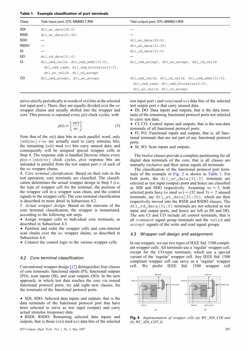
Table 1: Example classification of port terminals
Class Test input port: DTL.MMBD.T.RW Test output port: DTL.MMBD.I.RW
SDI dtl_wr_data[29:0] —
RSDI dtl_wr_data[31:30] —
SDO — dtl_wr_data[29:0]
RSDO — dtl_wr_data[31:30]
DI — dtl_rd_data[31:0]
DO dtl_rd_data[31:0] —
CI dtl_cmd_valid, dtl_cmd_addr[31:0],
dtl_cmd_read, dtl_cmd_blocksize[5:0],
dtl_wr_valid, dtl_rd_accept
dtl_cmd_accept, dtl_wr_accept, dtl_rd_valid
CO dtl_cmd_accept, dtl_wr_accept dtl_cmd_valid, dtl_rd_valid, dtl_cmd_addr[31:0],
dtl_cmd_read, dtl_cmd_blocksize[5:0],
dtl_wr_valid, dtl_rd_accept
arrive strictly periodically in words ofw(i) bits at the selectedtest input port i. There, they are equally divided over the wcwrapper chains and serially shifted into the wrapper andcore. This process is repeated every p(i) clock cycles, with
p(i) ¼w(i)
wc
� �(3)
Note that of the w(i) data bits in each parallel word, onlybw(i)=wcc � wc are actually used to carry stimulus bits;the remaining (w(i) mod wc) bits carry unused data, andconsequently will be assigned special wrapper cells inStep 4. The response side is handled likewise where everyp(o) ¼ bw(o)=wcc clock cycles, p(o) response bits areunloaded in parallel from the test output port o of each ofthe wc wrapper chains.4. Core terminal classification: Based on their role in thetest operation, core terminals are classified. The classifi-cation determines the actual wrapper design in Step 5 (i.e.the type of wrapper cell for the terminal, the position ofthe wrapper cell in a wrapper scan chain, and the controlsignals to the wrapper cell). The core terminal classificationis described in more detail in Subsection 4.2.5. Actual wrapper design: Based on the outcome of thecore terminal classification, the wrapper is instantiated,according to the following sub steps.† Assign wrapper cells to individual core terminals, asdescribed in Subsection 4.3.† Partition and order the wrapper cells and core-internalscan chains over the wc wrapper chains, as described inSubsection 4.4.† Connect the control logic to the various wrapper cells.
4.2 Core terminal classification
Conventional wrapper design [17] distinguishes four classesof core terminals: functional inputs (FI), functional outputs(FO), scan inputs (SI), and scan outputs (SO). In the newapproach, in which test data reaches the core via reusedfunctional protocol ports, we add eight new classes, forthe terminals of the functional protocol ports.
† SDI, SDO: Selected data inputs and outputs, that is thedata terminals of the functional protocol port that havebeen selected to serve as test input (output) and carryactual stimulus (response) data.† RSDI, RSDO: Remaining selected data inputs andoutputs, that is those (w(i) mod wc) data bits of the selected
IET Comput. Digit. Tech., Vol. 1, No. 3, May 2007
test input port i and (w(o) mod wc) data bits of the selectedtest output port o that carry unused data.† DI, DO: Data inputs and outputs, that is the data term-inals of the remaining functional protocol ports not selectedto carry test data.† CI, CO: Control inputs and outputs, that is the non-dataterminals of all functional protocol ports.† FI, FO: Functional inputs and outputs, that is, all func-tional terminals that are not part of any functional protocolports.† SI, SO: Scan inputs and outputs.
The twelve classes provide a complete partitioning for alldigital data terminals of the core, that is all classes aremutually exclusive and their union equals all terminals.
The classification of the functional protocol port term-inals of the example in Fig. 2 is shown in Table 1. Forboth ports, the dtl_wr_data[31:0] terminals areselected as test input (output) ports and hence are classifiedas SDI and SDO respectively. Assuming wc ¼ 3, bothselected ports have (w mod wc) ¼ (32 mod 3) ¼ 2 unusedterminals, say dtl_wr_data[31:30], which are thenrespectively moved into the RSDI and RSDO classes. Thedtl_rd_data[31:0] terminals are not selected as testinput and output ports, and hence are left as DI and DO.The sets CI and CO include all control terminals, that isall command signal group terminals and the valid andaccept signals of the write and read signal groups.
4.3 Wrapper cell design and assignment
In our wrapper, we use two types of IEEE Std. 1500 compli-ant wrapper cells. All terminals use a ‘regular’ wrapper cell,except for the CO-type terminals, which use a specialvariant of the ‘regular’ wrapper cell. Any IEEE Std. 1500compliant wrapper cell can serve as a ‘regular’ wrappercell. We prefer IEEE Std. 1500 wrapper cell
Fig. 4 Implementation of wrapper cells (a) WC_SDI_COI and(b) WC_SDI_COT_G
201

Table 2: Control generator parameters for test output port DTL.MMBD.I.RW
Terminal Parameters(v, p) Description
dtl_cmd_valid (1, s(o)� p(o)) Every s(o) words, a new command is issued
dtl_cmd_addr[31:0] ‘0’ ¼ (0, 1) Address is not used and hence kept at ‘0’
dtl_cmd_read ‘0’ ¼ (0, 1) Only the write side of this port is used and hence read ¼ 0
dtl_cmd_blocksize[6] (s(o), 1) Block size is s(o)
dtl_wr_valid (1, p(o)) Every p(o) clock cycles, a new word with test responses is available
dtl_rd_accept ‘0’ ¼ (0, 1) The read size of this port is not used and hence accept ¼ 0
WC_SD1_COI [18], as depicted in Fig. 4a. This wrappercell is small (one flip-flop only) and the combined activationof INTEST and EXTEST modes guarantees full testcoverage of the wrapper cell itself, as the captured signalis tapped off after the functional multiplexer.
The CO-type core terminals require a special variant ofthe ‘regular’ wrapper cell because they need to assurethat, as far as the on-chip bus or NOC is concerned, alsoin test mode, the functional port protocol is handled asnormal, such that the transport of test data is not interrupted.For example, the valid/accept handshakes of thecommand, write, and read groups of a DTL port need tobe completed as usual. The special wrapper cell forCO-type terminals consists of a generic part and a terminal-specific part. The generic part is a guarded variant of the‘regular’ wrapper cell. For our preferred wrapper cellWC_SD1_COI, the guarded variant is IEEE Std. 1500wrapper cell WC_SD1_COI_G as depicted in Fig.4b.Its functional output can be set to the value of signalprot-value. The circuitry that generates prot-valueis specific for each CO terminal.
The generic version of the control generator has a periodicoutput behaviour, which is characterised by a binary-codedoutput value v and a period p. For p – 1 consecutive clockcycles, the output value is �v, while for the next clock cycle,the output is v. The hardware implementation uses asimple counter. Some CO terminals require hard-coded‘0’or ‘1’ signals; this is captured by (v, p) ¼ (0, 1) and(v, p) ¼ (1, 1), respectively. The control generatorimplementation for these signals uses tie-off-cells.
Table 2 describes for the selected test output port of ourexample in Fig. 2 which output signals are required on itsCO-type terminals in order to keep the functional port pro-tocol running. The port is used as an output via itsdtl_wr_data terminals, and hence dtl_cmd_read iskept at a hard-coded ‘0’. Every p(o) clock cycles, a newword with test responses is available for parallel read-outfrom the scan chains. To write this word to the interconnectdtl_wr_valid is ‘l’ every p(o) clock cycles. The speci-fied bandwidth bout(o) is achieved for a given block sizes(o). Hence, the binary six-bit equivalent of s(o) is outputon dtl_cmt_blocksize[6]. Every (s(o) � p(o))cycles, a block of s(o) words has been output, and thisinitiator port should issue a new command, in order toinstruct the bus or NOC to accept another block. Terminalsdtl_cmd_addr[31:0] and dtl_rd_accept are notused, and hence kept at hard-coded ‘0’.
4.4 Partitioning and ordering of wrapper chainitems per wrapper chain
Wrapper chains are made up from wrapper cells andcore-internal scan chains. We need to construct wcwrapper chains, but typically many more than wc wrapperchain items exist. Hence, we need to partition the wrappercells and core-internal scan chains over the wc wrapper
202
chains, and subsequently determine the order of the itemsper wrapper chain. Our approach to do this is a modificationof the conventional wrapper design optimisation algorithmof [17].
In conventional wrapper design, the test length Tconv for awrapped core is defined as
Tconv ¼ (1 þ max (si, so)) � pat þ min (si, so) (4)
where pat denotes the number of test patterns, and si and sodenote the scan-in and scan-out length for the wrapped core,respectively [17]. To minimise Tconv, both si and so must beminimised. All wrapper input cells and all core-internalscan chains participate in a scan-in-operation and hencemight contribute to si; likewise, all wrapper output cellsand core-internal scan chains participate in a scan-out oper-ation and therefore might contribute to so. The conventionalpartitioning algorithm in [17] first addresses the NP-hardproblem of partitioning the core-internal scan chains overthe available number of to-be-constructed wrapper chains,before partitioning the wrapper input and output cells.This approach aims to minimise both si and so. The sub-sequent step of ordering of wrapper items per wrapperchain is done such that the wrapper input cells are followedby the core-internal scan chains, which in turn are followedby the wrapper output cells. A schematic view of the result-ing conventional wrapper chain is depicted in Fig. 5a.
A schematic view of the wrapper chains resulting fromour new wrapper design approach is shown in Fig. 5b.The main differences are formed by the category of SDIwrapper input cells, through which stimuli are loaded intothe wrapper chain in a parallel fashion, and the categoryof SDO wrapper output cells, through which responses areunloaded from the wrapper chain in a parallel fashion.
† The test stimuli of a test pattern arrive at regular intervalsof p(i) clock cycles at the SDI wrapper input cells. All of themare shifted into the wrapper chains, apart from the last word,which can be directly consumed in parallel for testing.
Fig. 5 Schematic view of conventional (a) and new (b) orderingof wrapper items per wrapper
IET Comput. Digit. Tech., Vol. 1, No. 3, May 2007

Similarly, for each test pattern the first word of responses isdirectly transported away in parallel from the SDO wrapperoutput cells, after which the subsequent words are shiftedout of the wrapper chains at regular intervals of p(o) clockcycles. Hence, the test length Tnew is redefined as
Tnew ¼ (1 þ max (ti, to)) � pat þ min (ti, to) (5)
with
ti ¼sip(i)
� �� 1
� �� p(i) þ 1 (6)
to ¼sop(o)
� �� 1
� �� p(o) þ 1 (7)
† In order to minimise the test length Tnew, the wrapperitems should be partitioned such that all SDI cells andall SDO cells are evenly distributed over the wcto-be-constructed wrapper chains.† For wrapper item ordering, it is important that all SDI cellsare placed at the start of the wrapper chain, as they are theentry point of stimuli into the wrapper chain, otherwise,some wrapper chain items are unreachable for scan access.Similarly, all SDO cells should be placed at the end of thewrapper chain.
Algorithmically, the partitioning of wrapper items is donein a five-step approach, which is clearly based on the three-step approach in [17].
1. Assign the core-internal scan chains to the wc wrapperchains, such that the maximum sum of scan lengths assignedto a wrapper chain is minimised. Algorithms like LPT andCOMBINE can be used [17]. The resulting partition isnamed Ps
2. Assign the wrapper input cells in RSDI < DI < CI < FIto the wc wrapper chains on top of Ps , such that themaximum scan-in length of all wrapper chains is mini-mised. The resulting partition is named Pin
wc
3. Assign the wrapper input cells in SDI to the wc wrapperchains on top of Pin
wc. The resulting partition is named Pin .
IET Comput. Digit. Tech., Vol. 1, No. 3, May 2007
4. Assign the wrapper output cells in RSDO < DO <CO < FO to the wc wrapper chains on top of Ps , suchthat the maximum scan-out length of all wrapper chains isminimised. The resulting partition is named Pout
wc
5. Assign the wrapper output cells in SDO to the wcwrapper chains on top of Pout
wc . The resulting partition isnamed Pout.
5 Experimental results
5.1 Simplified illustrative example
We have implemented our wrapper design for a simplifiedillustrative example core and NOC. The NOC is anautomatically generated, simple Æthereal network [8], con-sisting of one router and four network interfaces, basedon a 32-bits data DTL protocol [2]. As depicted in Fig. 6a,two NOC ports connect to the ATE source and sink,respectively, while the two other ports connect to the CUT.
The CUT has two DTL ports, Port 1 and Port 2, with 133terminals each and a functional data word width w ¼ 32.Besides the two ports, the CUT has no other functionalterminals. The CUT has five internal scan chains oflengths 123, 123, 50, 50, and 23 flip-flops, and pat ¼ 10.Port 1 is selected to receive stimuli and Port 2 is selectedto send out responses. The test data flow for stimuli isfrom the source through the NOC into the CUT viaPort 1, while test responses flow from the CUT’s Port 2via the NOC into the sink. bin(1) ¼ 1600 Mbits/s,bout(2) ¼ 2400 Mbits/s, and f ¼ 500 MHz, and (as perEquation (2)), we can afford a wrapper with wc ¼ 3wrapper chains. As per Equation (3), test data arrives withperiod p(1) ¼ p(2) ¼ 10 clock cycles. For Port 1:jSDIj ¼ 30, jRSDIj ¼ 2, jDOj ¼ 32, jCIj ¼ 62, andjCOj ¼ 7. For Port 2: jSDOj ¼ 30, jRSDOj ¼ 2,jDIj ¼ 32, jCIj ¼ 7, and jCOj ¼ 62. The wrapper chainscan lengths are si ¼ so ¼ 168. The resulting wrapperdesign is shown in Fig. 6b. As per Equation (5), testlength Tnew ¼ 1781 clock cycles. Note that this representsa 4.1% test length reduction compared to a conventionalwrapper design with three wrapper chains, which would
Fig. 6 Illustrative example consisting of a NOC and CUT and b the detailed wrapper design for the CUT
203

have a test length Tconv ¼ 1858 clock cycles. This reductionis because of the fact that the last stimulus word of eachpattern is loaded in parallel into the SDI wrapper cellsand does not require any further shifting in, and likewisethe first response word of each pattern is loaded in parallelinto the SDO wrapper cells.
Our example was implemented in register-transfer-levelVHDL and verified through simulation. The experimentshowed a modest area increase for the new wrapper incomparison to a conventional wrapper. The number of gate-equivalents required to implement all wrapper cells wentfrom 2910 to 3000 (an increase of þ3.1%), while 489 gate-equivalents were required to implement the additionalcontrol logic to complete correct protocol operation. Thetotal relative wrapper area increase was þ19.9%. Notethat wrappers are typically small compared to the overallSOC size, and hence, this area impact is negligible at theSOC level.
5.2 Wrapper area and core test length impact
In this section, we present wrapper area and core test lengthresults from our new wrapper design approach in compari-son with conventional wrapper design, obtained on a largesubset of cores in the ITC’02 SOC test benchmarks [38].A wrapper design and optimisation tool as described inthis paper has been developed in Cþþ; it uses theCOMBINE wrapper design routine [17] as a basis. The toolcalculates the required number of gate-equivalents todesign the wrapper and the resulting test length in clockcycles. We do this for both the conventional wrapperdesign approach, which relies on a dedicated TAM, aswell as for our new wrapper design approach, whichreuses the functional protocol ports of the core.
The cores in the ITC’02 benchmarks do not have func-tional protocol ports (or, at least, they are not specified),while our method critically depends on their presence.Hence, we assume that every core has two DTL ports,of which one serves as a test input and the other as atest output. The assumed DTL test input port has 32SDI terminals, 45 CI terminals, and 2 CO terminals.The assumed DTL test output port has 32 SDO terminals,2 CI terminals, and 45 CO terminals. For the two DTLports, each core needs 79 input terminals and 79 outputterminals. Some of the 186 cores in the ITC’02 bench-marks do not have that many terminals and hence are
204
not considered in our evaluation. Cores withbi-directional terminals are also not considered. Thisstill leaves 42 cores for our experiments, which arelisted in Table 3.
We assume that bandwidths bin(i) and bout(o) and testfrequency f are such that the maximum affordablenumber of wrapper chains wc ¼ 16. Asw(i) ¼ w(o) ¼ 32, wc ¼ 16 implies that p(i) ¼ p(o) ¼ 2.However, it is also possible to implement fewer, butlonger wrapper chains, which means that we are notusing the bandwidth to its maximum, and consequentlyaccept a longer test length.
For all 42 cores considered and for a number of wrapperchains wc ranging from 1 to 16, we have calculated thenumber of gate-equivalents required to implement awrapper and the corresponding test length in clockcycles, for both the conventional wrapper design algorithm[17] and our new approach. In total, this involves42 � 16 � 2 ¼ 1344 wrapper calculations. Fig. 7 showsthe average relative gate-equivalent count increase and therelative test length increase. The horizontal axes refer tocores with numbers in the order in which they are listedin Table 3.
Fig. 7a shows the increase in the number of gate-equivalents required to implement the new wrapper, relative
Table 3: List of considered ITC’02 SOC test benchmarks[17] cores
SOC Cores considered
a586710 2, 3, 4, 7
d281 7
d695 2
f2126 1, 2
g1023 1, 2, 3, 4, 10, 11, 12, 14
h953 1
p22810 27
p34392 2, 10, 18
p93791 10, 32
q12710 1, 2, 3, 4
t512505 1, 2, 4, 8, 9, 14, 15, 16, 17, 23, 24,
25, 26, 29, 31
Fig. 7 Proposed new wrapper design, compared to the conventional wrapper design, for 42 ITC’02 SOC test benchmark cores andwc [ [1. . .16]
a Average relative wrapper’s gate-equivalent count increaseb Relative core’s test length increase
IET Comput. Digit. Tech., Vol. 1, No. 3, May 2007

to what was required for a conventional wrapper design.These numbers show only around 1% variation forvarying values of wc, and hence we have decided to showthe average increase for 1 � wc � 16. The averagewrapper area increase over all 672 cases is 14.5%, whichis negligible at the SOC level. Fig. 7b shows that the testlength impact of the new approach varies between 227.4and þ7.2% with, on average over all 672 cases, a testlength decrease of 3.8%.
6 Conclusion
In this paper, we have proposed a core test wrapper designthat allows test data to be transported via functional protocolports, such as AXI, DTL, and OCP ports. This approachallows test data transport via an existing functionalon-chip bus, NOC, or other functional interconnect. Wehave assumed that the functional interconnect connects tothe test source and sink, be it either an external ATE, oron-chip BIST engine. We have required that the bus,NOC, or other functional interconnect provide guaranteedbandwidth and constant latency, which is necessary tooperate streaming scan tests. We have exploited the avail-able functional bandwidth as much as possible in order tominimise the core’s test length.
Our new wrapper design no longer relies on a dedicatedTAM, and hence has no dedicated TAM ports. Instead,the test data is transported via selected functional protocolports. This requires careful wrapper design, such that thenumber of wrapper chains is tuned to the available testdata bandwidth; the functional protocols are correctly exe-cuted while the test is running; and the protocol portwrapper cells are positioned at the head and tail of thevarious wrapper chains.
Although other papers have described the reuse of func-tional buses and NOCs as a TAM, no previous papershave worked out the details of the wrapper design for thisscenario. The benefits of our approach are that no dedicatedTAM is required, that test access to the embedded coresis guaranteed, and that the test expansion becomessimpler. By using guaranteed communication services, ourapproach hides any internal details of the functional inter-connect. For the functional interconnect, the transport oftest data is just another application, enabling unchangedre-use of the functional interconnect design flow.
The implementation of the new wrapper design for 672example cases based on the ITC’02 SOC test benchmarksshowed an average wrapper area increase of 14.5%, com-pared to a conventional wrapper. Note that at the SOClevel, this area increase is negligible. The same 672example cases show an average reduction of test lengthof 3.8%.
7 Acknowledgments
This work was partially supported by the Brazilian fundingagencies CAPES and CNPq-PNM, under scholarship grants2371/04-9 and 141993/2002-2, respectively, and by theEuropean MEDEAþ NanoTest project.
8 References
1 ARM: AMBA AXI Protocol Specification, 20032 Philips Semiconductors: Device transaction level (DTL) protocol
specification Version 2.2, 20023 OCP International Partnership: Open core protocol specification 2.0
release candidate, 20034 Benini, L., and De Micheli, G.: ‘Networks-on-chips: a new SOC
Paradigm’, IEEE Computer, 2002, 35, (1), pp. 70–80
IET Comput. Digit. Tech., Vol. 1, No. 3, May 2007
5 Jantsch, A., and Tenhunen, H. (Eds.): ‘Networks on Chip’ (KluwerAcademic Publishers, 2003)
6 Nurmi, J., Tenhunen, H., Isoaho, J., and Jantsch, A. (Eds.):‘Interconnect-centric design for advanced SoC and NoC’ (KluwerAcademic Publishers, 2004)
7 De Micheli, G., and Benini, L. (Eds.): ‘Networks on chips: technologyand tools’ (The Morgan Kaufmann Series in Systems on Silicon,Morgan Kaufman, 2006)
8 Goossens, K., Dielissen, J., and Radulescu, A.: ‘The Æthereal networkon chip: concepts, architectures, and implementations’, IEEE Design& Test of Computers, 2005, 22, (5), pp. 21–31
9 Bjerregaard, T., and Sparsf, J.: ‘A router architecture forconnection-oriented service guarantees in the MANGO clocklessnetwork-on-chip’. Proc. Design, Automation, and Test in Europe,Munich, Germany, 2005, pp. 1226–1231
10 Millberg, M., Nilsson, E., Thid, R., and Jantsch, A.: ‘Guaranteedbandwidth using looped containers in temporally disjoint networkswithin the nostrum network on chip’. Proc. Design, Automation,and Test in Europe, Paris, France, 2004, pp. 890–895
11 Laffely, A., Liang, J., Tessier, R., and Burleson, W.: ‘Adaptive systemon a chip (aSOC): a backbone for power-aware signal processingcores’. Int. Conf. on Image Processing, Barcelona, Spain, 2003,pp. 105–108
12 Weber, W.D., Chou, J., Swarbrick, I., and Wingard, D.: ‘Aquality-of-service mechanism for interconnection networks insystem-on-chips’. Proc. Design, Automation, and Test in Europe,Munich, Germany, 2005, pp. 1232–1237
13 Goossens, K., Dielissen, J., van Meerbergen, J., Paplavko, P.,Radulescu, A., Rijpkema, E., Waterlander, E., and Wielage, P.:‘Guaranteeing the quality of services in networks on chip’ inJantsch, A., and Tenhunen, H. (Eds.): ‘Networks on chip’ (KluwerAcademic Publishers, 2003), pp. 61–82
14 Marinissen, E.J., and Zorian, Y.: ‘Challenges in testing core-basedsystem ICs’, IEEE Commun. Mag., 1999, 37, (6), pp. 104–109
15 Marinissen, E.J., and Waayers, T.: ‘Infrastructure for modular SOCtesting’. Proc. IEEE Custom Integrated Circuits Conf., Orlando, FL,USA, 2004, pp. 671–678
16 Marinissen, E.J., Arendsen, R., Bos, G., Dingemanse, H., Lousberg,M., and Wouters, C.: ‘A structured and scalable mechanism for testaccess to embedded reusable cores’. Proc. IEEE Int. Test Conf.,Washington, DC, USA, 1998, pp. 284–293
17 Marinissen, E.J., Goel, S.K., and Lousberg, M.: ‘Wrapper design forembedded core Test’. Proc. IEEE Int. Test Conf., Atlantic City, NJ,USA, 2000, pp. 911–920
18 Da Silva, F. (Ed.): ‘IEEE Std. 1500TM-2005 standard testabilitymethod for embedded core-based integrated circuits’ (IEEE,New York, NY, USA, 2005)
19 Goel, S.K., and Marinissen, E.J.: ‘Effective and efficient testarchitecture design for SOCs’. Proc. IEEE Int. Test Conf.,Baltimore, MD, USA, 2002, pp. 529–538
20 Harrod, P.: ‘Testing reusable IP—a case study’. Proc. IEEE Int. TestConf., Atlantic City, NJ, USA, 1999, pp. 493–498
21 Huang, J.R., Iyer, M.K., and Cheng, K.T.: ‘A self-test methodologyfor IP cores in bus-based programmable SOCs’. Proc. IEEE VLSITest Symp. Marina del Rey, CA, USA, 2001, pp. 198–203
22 Hwang, S., and Abraham, J.A.: ‘Reuse of addressable system bus forSOC testing’. Proc. IEEE Int. ASIC/SOC Conf., Washington, DC,USA, 2001, pp. 215–219
23 Amory, A.M., Oliveira, L.A., and Moraes, F.G.: ‘Software-based testfor non-programmable cores in bus-based system-on-chiparchitectures’. Proc. IFIP Int. Conf. on Very Large ScaleIntegration, Darmstadt, Germany, 2003, pp. 174–179
24 Feige, C., ten Pierick, J., Wouters, C., Tangelder, R., and Kerkhoff, H.:‘Integration of the scan-test method into an architecture specificcore-test approach’. Digest of papers of IEEE European TestWorkshop, Barcelona, Spain, 1998, pp. 241–245
25 Hughes, P., Harrod, P., and Campbell, G.: ‘Embedded CPU teststrategies’. Digest of Papers of IEEE European Test Workshop,Corfu, Greece, 2002, pp. 281–285
26 Cota, E., Kreutz, M., Zeferino, C., Carro, L., Lubaszewski, M., andSusin, A.: ‘The impact of NoC reuse on the testing of core-basedsystems’. Proc. IEEE VLSI Test Symp. Napa, CA, USA, 2003,pp. 128–133
27 Cota, E., Carro, L., Wagner, F., and Lubaszewski, M.: ‘Power-awareNoC reuse on the testing of core-based systems’. Digest of Papers ofIEEE European Test Workshop, Maastricht, The Netherlands, 2003,pp. 123–128
28 Cota, E., Carro, L., Wagner, F., and Lubaszewski, M.: ‘Power-awareNoC reuse on the testing of core-based systems’. Proc. IEEE Int. TestConf., Charlotte, NC, USA, 2003, pp. 612–621
29 Liu, C., Cota, E., Sharif, H., and Pradhan, D.: ‘Test schedulingfor network-on-chip with BIST and precedence constraints’. In Proc.IEEE Int. Test Conf., Charlotte, NC, USA, 2003, pp. 1369–1378
205

30 Liu, C., Iyengar, V., Shi, J., and Cota, E.: ‘Power-aware test schedulingin network-on-chip using variable-rate on-chip clocking’. Proc. IEEEVLSI Test Symp., Palm Springs, CA, USA, 2005, pp. 349–354
31 Liu, C., and Iyengar, V.: ‘Test scheduling with thermal optimizationfor network-on-chip using variable-rate on-chip clocking’. Proc.Design Automation, and Test in Europe, Munich, Germany, 2006,pp. 652–657
32 Kim, J.S., Hwang, M.S., Roh, S., Lee, J.Y., Lee, K., Lee, S.J.,and Yoo, H.J.: ‘On-chip network based embedded core testing’.Proc. IEEE Int. SOC Conf., Santa Clara, CA, USA, 2004,pp. 223–226
33 Goossens, K., Dielissen, J., Gangwal, O.P., Pestana, S.G., Radulescu,A., and Rijpkema, E.: ‘A design flow for application-specific networkson chip with guaranteed performance to accelerate SOC design andverification’. Proc. Design Automation, and Test in Europe, Munich,Germany, 2005, pp. 1182–1187
34 Nahvi, M., and Ivanov, A.: ‘A packet switching communication-based test access mechanism for system chips’. Digest of Papers ofIEEE European Test Workshop, Saltsjobaden, Sweden, 2001,pp. 195–200
206
35 Hosseinabady, M., Banaiyan, A., Bojnordi, M.N., and Navabi, Z.: ‘Aconcurrent testing method for NoC switches’. Proc. DesignAutomation, and Test in Europe, Munich, Germany, 2006,pp. 1171–1176
36 Radulescu, A., Dielissen, J., Pestana, S.G., Gangwal, O.P., Rijpkema,E., Wielage, P., and Goossens, K.: ‘An efficient on-chip networkinterface offering guaranteed services, shared-memory abstraction,and flexible network programming’, IEEE Trans. CAD Integr. Circ.Syst., 2005, 24, (1), pp. 4–17
37 Coenen, M., Murali, S., Radulescu, A., Goossens, K., andde Micheli, G.: ‘A Buffer-sizing algorithm for networks on chipusing TDMA and credit-based end-to-end flow-control’. Proc. Int.Conf. on Hardware-software Codesign and System Synthesis, Seoul,Korea, 2006, pp. 130–135
38 Marinissen, E.J., Iyengar, V., and Chakrabarty, K.: ‘A set ofbenchmarks for modular testing of SOCs’. Proc. IEEE Int. TestConf., Baltimore, MD, USA, 2002, pp. 519–528
39 da Silva, F., McLaurin, T., and Waayers, T.: ‘The core test wrapperhandbook – rationale and application of IEEE Std. 1500TM’(Springer Science+Business Media, LLC, 2006)
IET Comput. Digit. Tech., Vol. 1, No. 3, May 2007