TLIN1022-Q1 Dual Local Interconnect Network (LIN ...
42
TLIN1022 MCU LIN Controller Or SCI/UART (1) VDD I/O MCU w/o pullup (2) VDD I/O MCU w/o pullup (2) RXD1 TXD1 RXD2 TXD2 EN2 GND I/O VDD I/O VDD VREG VDD VSUP VBAT VSUP 200 pF 200 pF SLAVE NODE VSUP NC NC 2 6 14 10 13 9 12 11 NC NC 8 1 3 4 7 5 LIN1 LIN2 LIN Bus LIN Bus EN1 TLIN1022 MCU LIN Controller Or SCI/UART (1) VDD I/O MCU w/o pullup (2) VDD I/O MCU w/o pullup (2) RXD1 TXD1 RXD2 TXD2 EN2 GND I/O VDD I/O VDD VREG VDD VSUP VBAT VSUP Master Node Pullup 1 N 200 pF 200 pF MASTER NODE VSUP NC NC 2 6 14 10 13 9 12 11 NC NC 8 1 3 4 7 5 LIN1 LIN2 LIN Bus LIN Bus Product Folder Order Now Technical Documents Tools & Software Support & Community An IMPORTANT NOTICE at the end of this data sheet addresses availability, warranty, changes, use in safety-critical applications, intellectual property matters and other important disclaimers. UNLESS OTHERWISE NOTED, this document contains PRODUCTION DATA. TLIN1022-Q1 SLLSEZ8C – DECEMBER 2017 – REVISED MAY 2020 TLIN1022-Q1 Dual Local Interconnect Network (LIN) Transceiver with Dominant State Timeout 1 1 Features 1• AEC-Q100 Qualified for automotive applications – Temperature: –40°C to 125°C ambient – HBM certification level: ±8 kV – CDM certification level: ±1.5 kV • Compliant to LIN 2.0, LIN 2.1, LIN 2.2, LIN 2.2 A and ISO/DIS 17987–4.2 (See SLLA491) • Conforms to SAEJ2602 recommended practice for LIN (See SLLA491) • Supports 12 V battery applications • LIN transmit data rate up to 20 kbps. • Wide operating ranges – 4 V to 36 V supply voltage – ±45 V LIN bus fault protection • Sleep mode: ultra-low current consumption allows wake-up event from: – LIN bus – Local wake up through EN • Power up and down glitch free operation • Protection features: – Under voltage protection on V SUP – TXD Dominant time out protection (DTO) – Thermal shutdown protection – Unpowered node or ground disconnection failsafe at system level. • Available in SOIC (14) package and leadless VSON (14) Package with improved automated optical inspection (AOI) capability 2 Applications • Body Electronics and Lighting • Hybrid electric vehicles and power train systems • Infotainment and Cluster • Appliances 3 Description The TLIN1022-Q1 is a Dual Local Interconnect Network (LIN) physical layer transceiver with integrated wake-up and protection features, complaint to LIN 2.0, LIN 2.1, LIN 2.2, LIN 2.2A and ISO/DIS 17987–4.2 standards. LIN is a single wire bidirectional bus typically used for low speed in- vehicle networks using data rates up to 20 kbps. The TLIN1022-Q1 is designed to support 12 V applications with wider operating voltage and additional bus-fault protection. The LIN receiver supports data rates up to 100 kbps for in-line programming. The TLIN1022-Q1 converts the LIN protocol data stream on the TXD input into a LIN bus signal using a current-limited wave-shaping driver which reduces electromagnetic emissions (EME). The receiver converts the data stream to logic level signals that are sent to the microprocessor through the open-drain RXD pin. Ultra-low current consumption is possible using the sleep mode which allows wake-up via LIN bus or pin. Device Information (1) PART NUMBER PACKAGE BODY SIZE (NOM) TLIN1022-Q1 SOIC (14) (D) 5.00 mm x 8.65 mm VSON (14) (DMT) 3.00 mm x 4.50 mm (1) For all available packages, see the orderable addendum at the end of the data sheet. Spacer Simplified Schematics, Master Mode Simplified Schematics, Slave Mode
-
Upload
khangminh22 -
Category
Documents
-
view
0 -
download
0
Transcript of TLIN1022-Q1 Dual Local Interconnect Network (LIN ...

TLIN1022
MCU
LIN Controller
Or
SCI/UART(1)
VDD I/O MCU w/o
pullup(2)
VDD I/O MCU w/o
pullup(2)
RXD1
TXD1
RXD2
TXD2
EN2
GNDI/O
VDD I/O
VDD
VREG
VDD
VSUP
VBAT VSUP
200 pF
200 pF
SLAVE
NODE
VSUP
NC NC
26 14 10
13
9
12
11
NC
NC8
1
3
4
7
5
LIN1
LIN2 LIN Bus
LIN Bus
EN1
TLIN1022
MCU
LIN Controller
Or
SCI/UART(1)
VDD I/O MCU w/o
pullup(2)
VDD I/O MCU w/o
pullup(2)
RXD1
TXD1
RXD2
TXD2
EN2
GNDI/O
VDD I/O
VDD
VREG
VDD
VSUP
VBAT VSUP
Master Node
Pullup
1 N
200 pF
200 pF
MASTER
NODE
VSUP
NC NC
26 14 10
13
9
12
11
NC
NC8
1
3
4
7
5
LIN1
LIN2 LIN Bus
LIN Bus
Product
Folder
Order
Now
Technical
Documents
Tools &
Software
Support &Community
An IMPORTANT NOTICE at the end of this data sheet addresses availability, warranty, changes, use in safety-critical applications,intellectual property matters and other important disclaimers. UNLESS OTHERWISE NOTED, this document contains PRODUCTIONDATA.
TLIN1022-Q1SLLSEZ8C –DECEMBER 2017–REVISED MAY 2020
TLIN1022-Q1 Dual Local Interconnect Network (LIN) Transceiver with Dominant StateTimeout
1
1 Features1• AEC-Q100 Qualified for automotive applications
– Temperature: –40°C to 125°C ambient– HBM certification level: ±8 kV– CDM certification level: ±1.5 kV
• Compliant to LIN 2.0, LIN 2.1, LIN 2.2, LIN 2.2 Aand ISO/DIS 17987–4.2 (See SLLA491)
• Conforms to SAEJ2602 recommended practice forLIN (See SLLA491)
• Supports 12 V battery applications• LIN transmit data rate up to 20 kbps.• Wide operating ranges
– 4 V to 36 V supply voltage– ±45 V LIN bus fault protection
• Sleep mode: ultra-low current consumption allowswake-up event from:– LIN bus– Local wake up through EN
• Power up and down glitch free operation• Protection features:
– Under voltage protection on VSUP
– TXD Dominant time out protection (DTO)– Thermal shutdown protection– Unpowered node or ground disconnection
failsafe at system level.• Available in SOIC (14) package and leadless
VSON (14) Package with improved automatedoptical inspection (AOI) capability
2 Applications• Body Electronics and Lighting• Hybrid electric vehicles and power train systems• Infotainment and Cluster• Appliances
3 DescriptionThe TLIN1022-Q1 is a Dual Local InterconnectNetwork (LIN) physical layer transceiver withintegrated wake-up and protection features, complaintto LIN 2.0, LIN 2.1, LIN 2.2, LIN 2.2A and ISO/DIS17987–4.2 standards. LIN is a single wirebidirectional bus typically used for low speed in-vehicle networks using data rates up to 20 kbps. TheTLIN1022-Q1 is designed to support 12 Vapplications with wider operating voltage andadditional bus-fault protection. The LIN receiversupports data rates up to 100 kbps for in-lineprogramming. The TLIN1022-Q1 converts the LINprotocol data stream on the TXD input into a LIN bussignal using a current-limited wave-shaping driverwhich reduces electromagnetic emissions (EME). Thereceiver converts the data stream to logic levelsignals that are sent to the microprocessor throughthe open-drain RXD pin. Ultra-low currentconsumption is possible using the sleep mode whichallows wake-up via LIN bus or pin.
Device Information(1)
PART NUMBER PACKAGE BODY SIZE (NOM)
TLIN1022-Q1SOIC (14) (D) 5.00 mm x 8.65 mm
VSON (14) (DMT) 3.00 mm x 4.50 mm
(1) For all available packages, see the orderable addendum atthe end of the data sheet.
SpacerSimplified Schematics, Master Mode
Simplified Schematics, Slave Mode

2
TLIN1022-Q1SLLSEZ8C –DECEMBER 2017–REVISED MAY 2020 www.ti.com
Product Folder Links: TLIN1022-Q1
Submit Documentation Feedback Copyright © 2017–2020, Texas Instruments Incorporated
Table of Contents1 Features .................................................................. 12 Applications ........................................................... 13 Description ............................................................. 14 Revision History..................................................... 25 Pin Configuration and Functions ......................... 36 Specifications......................................................... 4
6.1 Absolute Maximum Ratings ...................................... 46.2 ESD Ratings.............................................................. 46.3 ESD Ratings - IEC .................................................... 46.4 Thermal Information .................................................. 46.5 Recommended Operating Conditions....................... 56.6 Electrical Characteristics........................................... 56.7 Switching Characteristics .......................................... 76.8 Timing Requirements ................................................ 76.9 Typical Characteristics .............................................. 8
7 Parameter Measurement Information .................. 98 Detailed Description ............................................ 18
8.1 Overview ................................................................. 18
8.2 Functional Block Diagram ....................................... 188.3 Feature Description................................................. 198.4 Device Functional Modes........................................ 21
9 Application and Implementation ........................ 249.1 Application Information............................................ 249.2 Typical Application ................................................. 24
10 Power Supply Recommendations ..................... 2511 Layout................................................................... 26
11.1 Layout Guidelines ................................................. 2611.2 Layout Example .................................................... 27
12 Device and Documentation Support ................. 2812.1 Documentation Support ....................................... 2812.2 Receiving Notification of Documentation Updates 2812.3 Support Resources ............................................... 2812.4 Trademarks ........................................................... 2812.5 Electrostatic Discharge Caution............................ 2912.6 Glossary ................................................................ 29
13 Mechanical, Packaging, and OrderableInformation ........................................................... 29
4 Revision HistoryNOTE: Page numbers for previous revisions may differ from page numbers in the current version.
Changes from Revision B (April 2020) to Revision C Page
• Added: (See SLLA491) to the Features list ........................................................................................................................... 1• Added : See errata TLIN1022-Q1 and TLIN2022-Q1 Duty Cycle Over VSUP......................................................................... 7
Changes from Revision A (January 2019) to Revision B Page
• Deleted Product Preview from the VSON (14) (DMT) pachage ............................................................................................ 1• Changed VLOGIC from max = 5.5 V to: 6 V in Absolute Maximum Ratings............................................................................. 4• Changed CLINPIN from max = 45 pF to max = 25 pF and added VSUP = 14 V for test condition in electrical
characteristics ........................................................................................................................................................................ 6
Changes from Original (December 2017) to Revision A Page
• Changed the VSON Body Size From: 3.00 mm x 3.00 mm To: 3.00 mm x 4.50 mm ........................................................... 1

1RXD1 14 NC
2EN1 13 LIN1
3TXD1 12 NC
4RXD2 11 NC
5EN2 10 VSUP
6NC 9 LIN2
7TXD2 8 GND
Not to scale
ThermalPad
1RXD1 14 NC
2EN1 13 LIN1
3TXD1 12 NC
4RXD2 11 NC
5EN2 10 VSUP
6NC 9 LIN2
7TXD2 8 GND
Not to scale
3
TLIN1022-Q1www.ti.com SLLSEZ8C –DECEMBER 2017–REVISED MAY 2020
Product Folder Links: TLIN1022-Q1
Submit Documentation FeedbackCopyright © 2017–2020, Texas Instruments Incorporated
5 Pin Configuration and Functions
D Package14-Pin (SOIC)
Top ViewDMT Package14-Pin (VSON)
Top View
Pin FunctionsPIN
Type DESCRIPTIONNO. NAME
1 RXD1 O Channel 1 RXD Output (open-drain) interface reporting state of LIN bus voltage2 EN1 I Channel 1 Enable Input3 TXD1 I Channel 1 TXD input interface to control state of LIN output4 RXD2 O Channel 2 RXD Output (open-drain) interface reporting state of LIN bus voltage5 EN2 I Channel 2 Enable Input7 TXD2 I Channel 2 TXD input interface to control state of LIN output8 GND GND Ground9 LIN2 HV I/O Channel 2 High voltage LIN bus single-wire transmitter and receiver10 VSUP Supply Device Supply Voltage (connected to battery in series with external reverse blocking diode)13 LIN1 HV I/O Channel 1 High voltage LIN bus single-wire transmitter and receiver
6, 11, 12,14 NC – Not Connected
4
TLIN1022-Q1SLLSEZ8C –DECEMBER 2017–REVISED MAY 2020 www.ti.com
Product Folder Links: TLIN1022-Q1
Submit Documentation Feedback Copyright © 2017–2020, Texas Instruments Incorporated
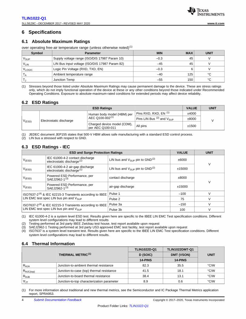
(1) Stresses beyond those listed under Absolute Maximum Ratings may cause permanent damage to the device. These are stress ratingsonly, which do not imply functional operation of the device at these or any other conditions beyond those indicated under RecommendedOperating Conditions. Exposure to absolute-maximum-rated conditions for extended periods may affect device reliability.
6 Specifications
6.1 Absolute Maximum Ratingsover operating free-air temperature range (unless otherwise noted) (1)
Symbol Parameter MIN MAX UNITVSUP Supply voltage range (ISO/DIS 17987 Param 10) –0.3 45 VVLIN LIN Bus input voltage (ISO/DIS 17987 Param 82) –45 45 VVLOGIC Logic Pin Voltage (RXD, TXD, EN) –0.3 6 VTA Ambient temperature range –40 125 °CTJ Junction Temp –55 150 °C
(1) JEDEC document JEP155 states that 500-V HBM allows safe manufacturing with a standard ESD control process.(2) LIN bus a stressed with respect to GND.
6.2 ESD RatingsESD Ratings VALUE UNIT
V(ESD) Electrostatic discharge
Human body model (HBM) perAEC Q100-002 (1)
Pins RXD, RXD, EN (1) ±4000
VPins LIN Bus (2) and VSUP ±8000Charged device model (CDM),per AEC Q100-011 All pins ±1500
(1) IEC 61000-4-2 is a system level ESD test. Results given here are specific to the IBEE LIN EMC Test specification conditions. Differentsystem level configurations may lead to different results
(2) Testing performed at 3rd party IBEE Zwickau test house, test report available upon request(3) SAEJ2962-1 Testing performed at 3rd party US3 approved EMC test facility, test report available upon request(4) ISO7637 is a system level transient test. Results given here are specific to the IBEE LIN EMC Test specification conditions. Different
system level configurations may lead to different results.
6.3 ESD Ratings - IECESD and Surge Protection Ratings VALUE UNIT
V(ESD)IEC 61000-4-2 contact dischargeelectrostatic discharge (1) LIN bus and VSUP pin to GND (2) ±6000
VV(ESD)
IEC 61000-4-2 air-gap dischargeelectrostatic discharge (1) LIN bus and VSUP pin to GND (2) ±15000
V(ESD)Powered ESD Performance, perSAEJ2962-1 (3) contact discharge ±8000
VV(ESD)
Powered ESD Performance, perSAEJ2962-1 (3) air-gap discharge ±15000
ISO7637-2 (4) & IEC 62215-3 Transients according to IBEELIN EMC test spec LIN bus pin and VSUP
Pulse 1 –100 VPulse 2 75 V
ISO7637-2 (4) & IEC 62215-3 Transients according to IBEELIN EMC test spec LIN bus pin and VSUP
Pulse 3a –150 VPulse 3b 100 V
(1) For more information about traditional and new thermal metrics, see the Semiconductor and IC Package Thermal Metrics applicationreport, SPRA953.
6.4 Thermal Information
THERMAL METRIC (1)TLIN1022D-Q1 TLIN1022DMT-Q1
UNITD (SOIC) DMT (VSON)14-PINS 14-PINS
RΘJA Junction-to-ambient thermal resistance 82.3 35.5 °C/WRΘJC(top) Junction-to-case (top) thermal resistance 41.5 18.1 °C/WRΘJB Junction-to-board thermal resistance 38.4 13.1 °C/WΨJT Junction-to-top characterization parameter 8.9 0.6 °C/W

5
TLIN1022-Q1www.ti.com SLLSEZ8C –DECEMBER 2017–REVISED MAY 2020
Product Folder Links: TLIN1022-Q1
Submit Documentation FeedbackCopyright © 2017–2020, Texas Instruments Incorporated
Thermal Information (continued)
THERMAL METRIC (1)TLIN1022D-Q1 TLIN1022DMT-Q1
UNITD (SOIC) DMT (VSON)14-PINS 14-PINS
ΨJB Junction-to-board characterization parameter 38.1 13.1 °C/WRΘJC(bot) Junction-to-case (bottom) thermal resistance n/a 2.5 °C/W
6.5 Recommended Operating Conditionsover operating free-air temperature range (unless otherwise noted)
PARAMETER - DEFINITION MIN NOM MAX UNITVSUP Supply voltage 4 36 VVLIN LIN Bus input voltage 0 36 VVLOGIC Logic Pin Voltage (RXD, TXD, EN) 0 5.25 VTSD Thermal shutdown edge 165 °CTSD(HYS) Thermal shutdown hysteresis 15 °C
6.6 Electrical Characteristicsover operating free-air temperature range (unless otherwise noted)
PARAMETER TEST CONDITIONS MIN TYP MAX UNITPower Supply
VSUPOperational supply voltage (ISO/DIS17987 Param 10)
Device is operational beyond the LINdefined nominal supply voltage rangeSee Figure 8 and Figure 9
4 36 V
VSUP
Nominal supply voltage (ISO/DIS 17987Param 10): Normal Mode: Ramp VSUPwhile LIN signal is a 10 kHZ SquareWave with 50 % duty cycle and 18Vswing.
Normal and Standby Modes: Ramp VSUPwhile LIN signal is a 10 kHZ SquareWave with 50 % duty cycle and 36Vswing. See Figure 8 and Figure 9
4 36 V
Sleep Mode 4 36 VUVSUP Under voltage VSUP threshold 2.9 3.85 V
UVHYSDelta hysteresis voltage for VSUP undervoltage threshold 0.2 V
ISUP Supply CurrentNormal Mode: EN = High, bus dominant:total bus load where RLIN > 500 Ω andCLIN < 10 nF See Figure 14
1.2 7.5 mA
ISUP Supply CurrentStandby Mode: EN = Low, bus dominant:total bus load where RLIN > 500 Ω andCLIN < 10 nF See Figure 14
1.1 3.75 mA
ISUP Supply Current Normal Mode: EN = High, BusRecessive: LIN = VSUP, 670 1300 µA
ISUP Supply Current Standby Mode: EN = Low, BusRecessive: LIN = VSUP, 20 40 µA
ISUP Supply Current Sleep Mode: 4.0 V < VSUP < 14 V, LIN =VSUP, EN = 0 V, TXD and RXD Floating 10 20 µA
ISUP Supply Current Sleep Mode: 14 V < VSUP < 36 V, LIN =VSUP, EN = 0 V, TXD and RXD Floating 30 µA
RXD OUTPUT PIN (OPEN DRAIN)VOL Output Low voltage Based upon External pull up to VCC 0.6 VIOL Low level output current, open drain LIN = 0 V, RXD = 0.4 V 1.5 mAIILG Leakage current, high-level LIN = VSUP, RXD = 5 V –5 0 5 µATXD INPUT PINVIL Low level input voltage –0.3 0.8 VVIH High level input voltage 2 5.5 V
VHYSInput threshold voltage, normal modes&selective wake modes 50 500 mV

6
TLIN1022-Q1SLLSEZ8C –DECEMBER 2017–REVISED MAY 2020 www.ti.com
Product Folder Links: TLIN1022-Q1
Submit Documentation Feedback Copyright © 2017–2020, Texas Instruments Incorporated
Electrical Characteristics (continued)over operating free-air temperature range (unless otherwise noted)
PARAMETER TEST CONDITIONS MIN TYP MAX UNITIILG Low level input leakage current TXD = Low –5 0 5 µARTXD Interal pulldown resitor value 125 350 800 kΩEN INPUT PINVIL Low level input voltage –0.3 0.8 VVIH High level input voltage 2 5.5 VVHYS Hysteresis voltage By design and characterization 50 500 mVIILG Low level input current EN = Low –5 0 5 µAREN Internal Pulldown resistor 125 350 800 kΩLIN PIN
VOH High level output voltage
LIN recessive, TXD = high, IO = 0 mA,VSUP = 7 V to 36 V 0.85 VSUP
LIN recessive, TXD = high, IO = 0 mA,VSUP = 4 V ≤ VSUP < 7 V 3.0 V
VOL Low level output voltage
LIN dominant, TXD = low, VSUP = 7 V to36 V 0.2 VSUP
LIN dominant, TXD = low, VSUP = 4 V ≤VSUP < 7 V 1.2 V
VSUP_NON_OPVSUP where Impact of recessive LINBus < 5% (ISO/DIS 17987 Param 11) TXD & RXD open LIN = 4 V to 45 V –0.3 45 V
IBUS_LIMLimiting current (ISO/DIS 17987 Param12)
TXD = 0 V, VLIN = 36 V, RMEAS = 440 Ω,VSUP = 36 V, VBUSdom < 4.518 VSee Figure 13
40 90 200 mA
IBUS_PAS_domReceiver leakage current, dominant(ISO/DIS 17987 Param 13)
LIN = 0 V, VSUP = 12 V Driveroff/recessive See Figure 14 –1 mA
IBUS_PAS_rec1Receiver leakage current, recessive(ISO/DIS 17987 Param 14)
LIN > VSUP, 8 V < VSUP < 36 V Driveroff; See Figure 15 20 µA
IBUS_PAS_rec2Receiver leakage current, recessive(ISO/DIS 17987 Param 14) LIN = VSUP, Driver off; See Figure 15 –5 5 µA
IBUS_NO_GNDLeakage current, loss of ground(ISO/DIS 17987 Param 15)
GND = VSUP, 0 V ≤ VLIN ≤ 18 V, VSUP =12 V; See Figure 16 –1 1 mA
IBUS_NO_BATLeakage current, loss of supply (ISO/DIS17987 Param 16)
0 V ≤ VLIN ≤ 36 V, VSUP = GND;See Figure 17 5 µA
VBUSdomLow level input voltage (ISO/DIS 17987Param 17)
LIN dominant (including LIN dominant forwake up) See Figure 10 and Figure 11 0.4 VSUP
VBUSrecHigh level input voltage (ISO/DIS 17987Param 18)
Lin recessive See Figure 10and Figure 11 0.6 VSUP
VBUS_CNTReceiver center threshold (ISO/DIS17987 Param 19)
VBUS_CNT = (VI_DOM + VI_REC)/2See Figure 10 and Figure 11 0.475 0.5 0.525 VSUP
VHYSHysteresis voltage (ISO/DIS 17987Param 20)
VHYS = (VI_REC - VI_DOM) See Figure 10and Figure 11 0.175 VSUP
VSERIAL_DIODESerial diode LIN term pullup path(ISO/DIS 17987 Param 21) By design and characterization 0.4 0.7 1 V
RSLAVEPullup resistor to VSUP (ISO/DIS 17987Param 26) Normal and Standby modes 20 45 60 kΩ
IRSLEEP Pullup current source to VSUP Sleep mode, VSUP = 14 V, LIN = GND –20 –2 µACLINPIN Capacitance of LIN pin VSUP = 14 V 25 pF

7
TLIN1022-Q1www.ti.com SLLSEZ8C –DECEMBER 2017–REVISED MAY 2020
Product Folder Links: TLIN1022-Q1
Submit Documentation FeedbackCopyright © 2017–2020, Texas Instruments Incorporated
(1) See errata TLIN1022-Q1 and TLIN2022-Q1 Duty Cycle Over VSUP(2) Duty cycles: LIN driver bus load conditions (CLINBUS, RLINBUS): Load1 = 1 nF, 1 kΩ; Load2 = 10 nF, 500 Ω. Duty cycles 3 and 4 are
defined for 10.4-kbps operation. The TLIN1022 also meets these lower data rate requirements, while it is capable of the higher speed20-kbps operation as specified by duty cycles 1 and 2. SAEJ2602 derives propagation delay equations from the LIN 2.0 duty cycledefinitions, for details see the SAEJ2602 specification
6.7 Switching Characteristics (1)
over operating free-air temperature range (unless otherwise noted)PARAMETER TEST CONDITIONS MIN TYP MAX UNIT
D112VDuty Cycle 1 (ISO/DIS 17987 Param27) (2)
THREC(MAX) = 0.744 x VSUP, THDOM(MAX)= 0.581 x VSUP, VSUP = 7 V to 18 V, tBIT= 50 µs (20 kbps), D1 = tBUS_rec(min)/(2 xtBIT) (See Figure 18 and Figure 19)
0.396
D112V Duty Cycle 1
THREC(MAX) = 0.625 x VSUP, THDOM(MAX)= 0.581 x VSUP, VSUP = 4 V to 7 V, tBIT =50 µs (20 kbps), D1 = tBUS_rec(min)/(2 xtBIT) (See Figure 18 and Figure 19)
0.396
D212V Duty Cycle 2 (ISO/DIS 17987 Param 28)
THREC(MIN) = 0.422 x VSUP, THDOM(MIN) =0.284 x VSUP, VSUP = 7.6 V to 18 V, tBIT= 50 µs (20 kbps), D2 = tBUS_rec(MAX)/(2 xtBIT) (See Figure 18 and Figure 19)
0.581
D312V Duty Cycle 3 (ISO/DIS 17987 Param 29)
THREC(MAX) = 0.778 x VSUP, THDOM(MAX)= 0.616 x VSUP, VSUP = 7 V to 18 V, tBIT= 96 µs (10.4 kbps), D3 = tBUS_rec(min)/(2x tBIT) (See Figure 18 and Figure 19)
0.417
D312V Duty Cycle
THREC(MAX) = 0.645 x VSUP, THDOM(MAX)= 0.616 x VSUP, VSUP = 4 V to 7 V, tBIT =96 µs (10.4 kbps), D3 = tBUS_rec(min)/(2 xtBIT) (See Figure 18 and Figure 19)
0.417
D412V Duty Cycle 4 (ISO/DIS 17987 Param 30)
THREC(MIN) = 0.389 x VSUP, THDOM(MIN) =0.251 x VSUP, VSUP = 7.6 V to 18 V, tBIT= 96 µs (10.4 kbps), D4 = tBUS_rec(MAX)/(2x tBIT) (See Figure 18 and Figure 19)
0.59
6.8 Timing RequirementsSYMBOL DESCRIPTION TEST CONDITIONS MIN NOM MAX UNIT
trx_pdrReceiver rising propagation delay time(ISO/DIS 17987 Param 31) RRXD = 2.4 kΩ, CRXD = 20 pF
(See Figure 20 and Figure 21)
6 µs
trx_pdfReceiver falling propagation delay time(ISO/DIS 17987 Param 31) 6 µs
trs_sym
Symmetry of receiver propagation delaytime Receiver rising propagation delaytime (ISO/DIS 17987 Param 32)
Rising edge with respect to falling edge,(trx_sym = trx_pdf – trx_pdr), RRXD = 2.4kΩ, CRXD = 20 pF (See Figure 20 andFigure 21)
–2 2 µs
tLINBUSLIN wakeup time (Minimum dominanttime on LIN bus for wakeup) See Figure 24, Figure 27 and Figure 28 25 100 150 µs
tCLEAR
Time to clear false wakeup preventionlogic if LIN bus had a bus stuckdominant fault (recessive time on LINbus to clear bust stuck dominant fault)
See Figure 28 8 17 50 µs
tDST Dominant state time out 20 34 80 ms
tMODE_CHANGE Mode change delay time
Time to change from standby mode tonormal mode or normal mode to sleepmode through EN pin: See Figure 22and Figure 29
2 15 µs
tNOMINT Normal mode initialization timeTime for normal mode to initialize anddata on RXD pin to be validSee Figure 22
35 µs
tPWR Power up time Upon power up time it takes for validdata on RXD 1.5 ms

VSUP Voltage Supply (V)
I SU
P S
up
ply
Cu
rre
nt (m
A)
0 5 10 15 20 25 30 35 40 45 50 55 600
0.5
1
1.5
2
2.5
3
3.5
D005
-55 °C27 °C125 °C
VSUP Voltage Supply (V)
I SU
P S
up
ply
Cu
rre
nt
(PA
)
0 5 10 15 20 25 30 35 40 45 505
6
7
8
9
10
11
12
13
D006
-55 °C27 °C125 °C
VSUP Voltage Supply (V)
I SU
P S
up
ply
Cu
rre
nt
(mA
)
0 5 10 15 20 25 30 35 40 45 500.5
1
1.5
2
2.5
3
3.5
4
4.5
5
5.5
6
D003
-55 °C27 °C125 °C
VSUP Voltage Supply (V)
I SU
P S
up
ply
Cu
rre
nt
(mA
)
0 5 10 15 20 25 30 35 40 45 500.4
0.45
0.5
0.55
0.6
0.65
0.7
0.75
0.8
0.85
0.9
0.95
1
1.05
1.1
D004
-55 °C27 °C125 °C
VSUP Voltage Supply (V)
VO
H (
V)
0 5 10 15 20 25 30 35 40 45 500
5
10
15
20
25
30
35
40
45
50
D001
Ch 1 (-55 °C)Ch 1 (27 °C)Ch 1 (125 °C)Ch 2 (-55 °C)Ch 2 (27 °C)Ch 2 (125 °C)
VSUP Voltage Supply (V)
VO
L (
V)
0 5 10 15 20 25 30 35 40 45 500.42
0.45
0.48
0.51
0.54
0.57
0.6
0.63
0.66
0.69
0.72
0.75
0.78
D002
Ch 1 (-55 °C)Ch 1 (27 °C)Ch 1 (125 °C)Ch 2 (-55 °C)Ch 2 (27 °C)Ch 2 (125 °C)
8
TLIN1022-Q1SLLSEZ8C –DECEMBER 2017–REVISED MAY 2020 www.ti.com
Product Folder Links: TLIN1022-Q1
Submit Documentation Feedback Copyright © 2017–2020, Texas Instruments Incorporated
6.9 Typical Characteristics
Figure 1. VOH vs VSUP and Temperature Figure 2. VOL vs VSUP and Temperature
Normal Mode (Dominant)
Figure 3. Supply Current vs Voltage Supply AcrossTemperature
Normal Mode (Recessive)
Figure 4. Supply Current vs Voltage Supply AcrossTemperature
Standby Mode (Dominant)
Figure 5. Supply Current vs Voltage Supply andTemperature
Standby Mode (Recessive)
Figure 6. Supply Current vs Voltage Supply andTemperature

Copyright © 2017, Texas Instruments Incorporated
Trigger PointDelta t = + 5 µs
(tBIT = 50 µs)
2 x tBIT = 100 µs (20 kBaud)
RX
Copyright © 2017, Texas Instruments Incorporated
1, 4
2, 5
3, 7
11, 12, 14
10
9, 13
8
Pulse Generator
tR/tF: Square Wave: < 20 ns
tR/tF: Triangle Wave: < 40nsFrequency: 20 ppm
Jitter: < 25 ns
Measurement ToolsO-scope:
DMM
Power SupplyResolution: 10mV/ 1mA
Accuracy: 0.2% VPS
5 VRXD1/2
TXD1/2
EN1/2
NC
NC
LIN1/2
GND
VSUP
6
VSUP Voltage Supply (V)
I SU
P S
up
ply
Cu
rre
nt
(PA
)
0 5 10 15 20 25 30 35 40 45 506
6.5
7
7.5
8
8.5
9
9.5
10
10.5
11
11.5
12
12.5
13
13.5
D007
-55 °C27 °C125 °C
9
TLIN1022-Q1www.ti.com SLLSEZ8C –DECEMBER 2017–REVISED MAY 2020
Product Folder Links: TLIN1022-Q1
Submit Documentation FeedbackCopyright © 2017–2020, Texas Instruments Incorporated
Typical Characteristics (continued)
Sleep Mode
Figure 7. Supply Current vs Voltage Supply and Temperature
7 Parameter Measurement Information
Figure 8. Test System: Operating Voltage Range with RX and TX Access: Parameters 9, 10
Figure 9. RX Response: Operating Voltage Range

Measurement ToolsO-scope:
DMM
Power Supply 1Resolution: 10 mV / 1mA
Accuracy: 0.2%
VPS1
5 V
Power Supply 2Resolution: 10 mV / 1mA
Accuracy: 0.2%
VPS2
D
RBUS
1, 4
2, 5
6
3, 7
11, 12, 14
10
9, 13
8
RXD1/2
TXD1/2
EN1/2
NC
NC
LIN1/2
GND
VSUP
Copyright © 2017, Texas Instruments Incorporated
Pulse Generator
tR/tF: Square Wave: < 20 ns
tR/tF: Triangle Wave: < 40 ns
Frequency: 20 ppmJitter: < 25 ns
Measurement Tools
O-scope: DMM
Power SupplyResolution: 10 mV / 1 mA
Accuracy: 0.2% VPS
5 V
1, 4
2, 5
6
3, 7
11, 12, 14
10
9, 13
8
RXD1/2
TXD1/2
EN1/2
NC
NC
LIN1/2
GND
VSUP
Copyright © 2017, Texas Instruments Incorporated
Period T = 1/f
Amplitude
(signal range)
Frequency: f = 20 Hz
Symmetry: 50%
LIN Bus Input
10
TLIN1022-Q1SLLSEZ8C –DECEMBER 2017–REVISED MAY 2020 www.ti.com
Product Folder Links: TLIN1022-Q1
Submit Documentation Feedback Copyright © 2017–2020, Texas Instruments Incorporated
Parameter Measurement Information (continued)
Figure 10. LIN Bus Input Signal
Figure 11. LIN Receiver Test with RX access Parameters 17, 18, 19, 20
Figure 12. VSUP_NON_OP Parameters 11

Copyright © 2017, Texas Instruments Incorporated
Measurement ToolsO-scope:
DMM
Power SupplyResolution: 10mV/ 1mA
Accuracy: 0.2%
VPS
RMEAS = 499
1, 4
2, 5
6
3, 7
11, 12, 14
10
9, 13
8
RXD1/2
TXD1/2
EN1/2
NC
NC
LIN1/2
GND
VSUP
Copyright © 2017, Texas Instruments Incorporated
Pulse GeneratortR/tF
: Square Wave: < 20 ns
tR/tF: Triangle Wave: < 40nsFrequency: 20 ppm
T = 10 ms
Jitter: < 25 ns
Measurement Tools
O-scope: DMM
Power Supply
Resolution: 10mV/ 1mAAccuracy: 0.2%
VPS
5 V
RMEAS
1, 4
2, 5
6
3, 7
11, 12, 14
10
9, 13
8
RXD1/2
TXD1/2
EN1/2
NC
NC
LIN1/2
GND
VSUP
11
TLIN1022-Q1www.ti.com SLLSEZ8C –DECEMBER 2017–REVISED MAY 2020
Product Folder Links: TLIN1022-Q1
Submit Documentation FeedbackCopyright © 2017–2020, Texas Instruments Incorporated
Parameter Measurement Information (continued)
Figure 13. Test Circuit for IBUS_LIM at Dominant State (Driver on) Parameters 12
Figure 14. Test Circuit for IBUS_PAS_dom; TXD = Recessive State VBUS = 0 V, Parameters 13

Measurement Tools
O-scope: DMM
Power Supply 1Resolution: 10mV/ 1mA
Accuracy: 0.2% VPS15 V
Power Supply 2
Resolution: 10mV/ 1mAAccuracy: 0.2%
VPS2
1 N
VPS2 2 V/s ramp [0 V à 27 V]
V Drop across resistor < 1V
1, 4
2, 5
6
3, 7
11, 12, 14
10
9, 13
8
RXD1/2
TXD1/2
EN1/2
NC
NC
LIN1/2
GND
VSUP
Copyright © 2017, Texas Instruments Incorporated
Measurement Tools
O-scope:
DMM
Power Supply 1
Resolution: 10mV/ 1mA
Accuracy: 0.2%
VPS1
Power Supply 2
Resolution: 10mV/ 1mA
Accuracy: 0.2%
VPS2
1 N
VPS2 2 V/s ramp
[8 V à 27 V]
V Drop across resistor
< 20 mV
1, 4
2, 5
6
3, 7
11, 12, 14
10
9, 13
8
TLINx022
RXD1/2
TXD1/2
EN1/2
NC
NC
LIN1/2
GND
VSUP
12
TLIN1022-Q1SLLSEZ8C –DECEMBER 2017–REVISED MAY 2020 www.ti.com
Product Folder Links: TLIN1022-Q1
Submit Documentation Feedback Copyright © 2017–2020, Texas Instruments Incorporated
Parameter Measurement Information (continued)
Figure 15. Test Circuit for IBUS_PAS_rec Param 14
Figure 16. Test Circuit for IBUS_NO_GND Loss of GND

Pulse Generator
tR/tF: Square Wave: < 20 ns
tR/tF: Triangle Wave: < 40 nsFrequency: 20 ppm
Jitter: < 25 ns
5 V
RMEAS
Power Supply 1Resolution: 10 mV / 1mA
Accuracy: 0.2% VPS1
Power Supply 2Resolution: 10 mV / 1mA
Accuracy: 0.2% VPS2
Measurement Tools
O-scope: DMM
1, 4
2, 5
6
3, 7
11, 12, 14
10
9, 13
8
RXD1/2
TXD1/2
EN1/2
NC
NC
LIN1/2
GND
VSUP
Copyright © 2017, Texas Instruments Incorporated
Measurement ToolsO-scope:
DMM
5 V
Power Supply 2
Resolution: 10mV/ 1mAAccuracy: 0.2%
VPS
10 N
VPS 2 V/s ramp [0 V à 27 V]
V Drop across resistor < 1V
1, 4
2, 5
6
3, 7
11, 12, 14
10
9, 13
8
RXD1/2
TXD1/2
EN1/2
NC
NC
LIN1/2
GND
VSUP
Copyright © 2017, Texas Instruments Incorporated
13
TLIN1022-Q1www.ti.com SLLSEZ8C –DECEMBER 2017–REVISED MAY 2020
Product Folder Links: TLIN1022-Q1
Submit Documentation FeedbackCopyright © 2017–2020, Texas Instruments Incorporated
Parameter Measurement Information (continued)
Figure 17. Test Circuit for IBUS_NO_BAT Loss of Battery
Figure 18. Test Circuit Slope Control and Duty Cycle Parameters 27, 28, 29, 30

Pulse GeneratortR/tF
: Square Wave: < 20 ns
tR/tF: Triangle Wave: < 40 ns
Frequency: 20 ppm
Jitter: < 25 ns
Measurement ToolsO-scope:
DMM
Power SupplyResolution: 10 mV / 1mA
Accuracy: 0.2%
VPS
5 V
VCC
2.4 N
20 pF
1, 4
2, 5
6
3, 7
11, 12, 14
10
9, 13
8
RXD1/2
TXD1/2
EN1/2
NC
NC
LIN1/2
GND
VSUP
Copyright © 2017, Texas Instruments Incorporated
TXD (Input)
RECESSIVE
DOMINANT
D = 0.5
tBITtBIT
THREC(MAX)
THREC(MIN)
THDOM(MAX)
THDOM(MIN)
tBUS_DOM(MAX) tBUS_REC(MAX)
tBUS_DOM(MIN) tBUS_REC(MIN)
LIN Bus
SignalVSUP
Thresholds
RX Node 1
Thresholds
RX Node 2
D = tBUS_REC(MIN)/(2 x tBIT)
D = tBUS_REC(MIN)/(2 x tBIT)
RXD: Node 1
D1 (20 kbps)
D3 (10.4 kbps)
RXD: Node 2
D2 (20 kbps)
D4 (10.4 kbps)
D112: 0.744 * VSUP
D312: 0.778 * VSUP
D112: 0.581 * VSUP
D312: 0.616 * VSUP
D212: 0.422 * VSUP
D412: 0.389 * VSUP
D212: 0.284 * VSUP
D412: 0.251 * VSUP
D124: 0.710 * VSUP
D324: 0.744 * VSUP
D124: 0.554 * VSUP
D324: 0.581 * VSUP
D224: 0.446 * VSUP
D424: 0.442 * VSUP
D224: 0.302 * VSUP
D424: 0.284 * VSUP
14
TLIN1022-Q1SLLSEZ8C –DECEMBER 2017–REVISED MAY 2020 www.ti.com
Product Folder Links: TLIN1022-Q1
Submit Documentation Feedback Copyright © 2017–2020, Texas Instruments Incorporated
Parameter Measurement Information (continued)
Figure 19. Definition of Bus Timing Parameters
Figure 20. Propagation Delay Test Circuit; Parameters 31, 32

Copyright © 2017, Texas Instruments Incorporated
Indetermin
ate Ignore
Standby
tMODE_CHANGE
tMODE_CHANGE
Transition Sleep
Floating
Transition
Indeterminate Ignore
EN
MODE
RXD Wake Request
RXD = Low
Wake Event
Normal Normal
Mirrors BusMirrors
Bus
tNOMINT
trx_pdf(1) trx_pdr(1)
THREC(MAX)
THREC(MIN)
THDOM(MAX)
THDOM(MIN)
LIN Bus
SignalVSUP
Thresholds
RX Node 1
Thresholds
RX Node 2
RXD: Node 1
D1 (20 kbps)
D3 (10.4 kbps)
RXD: Node 2
D2 (20 kbps)
D4 (10.4 kbps)
trx_pdr(2) trx_pdf(2)
Copyright © 2017, Texas Instruments Incorporated
15
TLIN1022-Q1www.ti.com SLLSEZ8C –DECEMBER 2017–REVISED MAY 2020
Product Folder Links: TLIN1022-Q1
Submit Documentation FeedbackCopyright © 2017–2020, Texas Instruments Incorporated
Parameter Measurement Information (continued)
Figure 21. Propagation Delay
Figure 22. Mode Transitions

VSUP
EN1/2
RXD1/2
LIN1/2
MODE
TXD1/2 Weak Internal Pulldown
Floating
Sleep NormalStandby
t < tLINBUS tLINBUS
0.4 x VSUP0.4 x
VSUP
0.6 x
VSUP
0.6 x
VSUP
VSUP
EN1/2
RXD1/2
LIN1/2
MODE
TXD1/2 Weak Internal Pulldown
Floating
Sleep
Weak Internal Pulldown
Normal
16
TLIN1022-Q1SLLSEZ8C –DECEMBER 2017–REVISED MAY 2020 www.ti.com
Product Folder Links: TLIN1022-Q1
Submit Documentation Feedback Copyright © 2017–2020, Texas Instruments Incorporated
Parameter Measurement Information (continued)
Figure 23. Wakeup Through EN
Figure 24. Wakeup through LIN

100 nF
RLIN2
CLIN2
RRXD2
CRXD2
RXD2
TXD2
VSUP
NC
LIN2
EN2
NC
GND
NC
NC
RRXD1
CRXD1
RXD1
EN1
TXD1
RLIN1
CLIN1
LIN1
17
TLIN1022-Q1www.ti.com SLLSEZ8C –DECEMBER 2017–REVISED MAY 2020
Product Folder Links: TLIN1022-Q1
Submit Documentation FeedbackCopyright © 2017–2020, Texas Instruments Incorporated
Parameter Measurement Information (continued)
Figure 25. Test Circuit for AC Characteristics

Comp
DR/
Slope
CTL
Dominant State
Timeout
Fault Detection & Protection
Filter
Wake Up
State & ControlEN1
NC
LIN1
RXD1
TXD1
VSUP/2
45 N
NC
Comp
DR/
Slope
CTL
Dominant State
Timeout
Fault Detection & Protection
Filter
Wake Up
State & ControlEN2
VSUP
LIN2
RXD2
TXD2
VSUP/2
45 N
NC
NC
VSUP
GND350 k
350 N
18
TLIN1022-Q1SLLSEZ8C –DECEMBER 2017–REVISED MAY 2020 www.ti.com
Product Folder Links: TLIN1022-Q1
Submit Documentation Feedback Copyright © 2017–2020, Texas Instruments Incorporated
8 Detailed Description
8.1 OverviewThe TLIN1022-Q1 device is a Dual Local Interconnect Network (LIN) physical layer transceiver, compliant to LIN2.0, LIN 2.1, LIN 2.2, LIN 2.2A and ISO/DIS 17987–4.2, with integrated wake-up and protection features. TheLIN bus is a single wire bidirectional bus typically used for low speed in-vehicle networks using data rates from2.4 kbps to 20 kbps. The device TLIN1022-Q1 LIN receiver works up to 100 kbps supporting in-lineprogramming. The LIN protocol data stream on the TXD input is converted by the TLIN1022-Q1 into a LIN bussignal using a current-limited wave-shaping driver as outlined by the LIN physical layer specification. Thereceiver converts the data stream to logic level signals that are sent to the microprocessor through the open-drain RXD pin. The LIN bus has two states: dominant state (voltage near ground) and recessive state (voltagenear battery). In the recessive state, the LIN bus is pulled high by the internal pull-up resistor (45 kΩ) and aseries diode. No external pull-up components are required for slave applications. Master applications require anexternal pull-up resistor (1 kΩ) plus a series diode per the LIN specification. The TLIN1022-Q1 provides manyprotection features such as ESD, EMC and high bus standoff voltage. The device also provides three methods towake up, EN and from the LIN bus.
8.2 Functional Block Diagram

Simplified Transceiver
Filter
VSUP
LIN
RXD
TXD
VSUP/2
350 N
45 N
Receiver
Transmitter with slope control
GND
1 N
VSUP
LIN Bus
VLIN_Dominant
VLIN_Recessive
VBattery
VSUP
t
VLIN_Bus
Voltage drop across the diodes in the pullup path
Copyright © 2017, Texas Instruments Incorporated
19
TLIN1022-Q1www.ti.com SLLSEZ8C –DECEMBER 2017–REVISED MAY 2020
Product Folder Links: TLIN1022-Q1
Submit Documentation FeedbackCopyright © 2017–2020, Texas Instruments Incorporated
8.3 Feature Description
8.3.1 LIN (Local Interconnect Network) BusThis high voltage input/output pin is a single wire LIN bus transmitter and receiver. The LIN pin can survivetransient voltages up to 45 V. Reverse currents from the LIN to supply (VSUP) are minimized with blocking diodes,even in the event of a ground shift or loss of supply (VSUP).
8.3.1.1 LIN Transmitter CharacteristicsThe transmitter has thresholds and AC parameters according to the LIN specification. The transmitter is a lowside transistor with internal current limitation and thermal shutdown. During a thermal shut-down condition, thetransmitter is disabled to protect the device. There is an internal pull-up resistor with a serial diode structure toVSUP, so no external pull-up components are required for the LIN slave mode applications. An external pull-upresistor and series diode to VSUP must be added when the device is used for a master node application.
8.3.1.2 LIN Receiver CharacteristicsThe receiver characteristic thresholds are proportional to the device supply pin according to the LIN specification.
The receiver is capable of receiving higher data rates (> 100 kbps) than supported by LIN or SAEJ2602specifications. This allows the TLIN1022-Q1 to be used for high speed downloads at the end-of-line production orother applications. The actual data rate achievable depends on system time constants (bus capacitance and pull-up resistance) and driver characteristics used in the system.
8.3.1.2.1 Termination
There is an internal pull-up resistor with a serial diode structure to VSUP, so no external pull-up components arerequired for the LIN slave mode applications. An external pull-up resistor (1 kΩ) and a series diode to VSUP mustbe added when the device is used for master node applications as per the LIN specification.
Figure 26 shows a Master Node configuration and how the voltage levels are defined
Figure 26. Master Node Configuration with Voltage Levels
8.3.2 TXD (Transmit Input and Output)TXD is the interface to the processors LIN protocol controller or SCI and UART that is used to control the state ofthe LIN output. When TXD is low the LIN output is dominant (near ground). When TXD is high the LIN output isrecessive (near VBattery). See Figure 26. The TXD input structure is compatible with processors using 3.3 V and 5V I/O. TXD has an internal pull-down resistor. The LIN bus is protected from being stuck dominant through asystem failure driving TXD low through the dominant state timer-out timer.

20
TLIN1022-Q1SLLSEZ8C –DECEMBER 2017–REVISED MAY 2020 www.ti.com
Product Folder Links: TLIN1022-Q1
Submit Documentation Feedback Copyright © 2017–2020, Texas Instruments Incorporated
Feature Description (continued)8.3.3 RXD (Receive Output)RXD is the interface to the processors LIN protocol controller or SCI and UART, which reports the state of theLIN bus voltage. LIN recessive (near VBattery) is represented by a high level on the RXD and LIN dominant (nearground) is represented by a low level on the RXD pin. The RXD output structure is an open-drain output stage.This allows the device to be used with 3.3 V and 5 V I/O processors. If the processors RXD pin does not have anintegrated pull-up, an external pull-up resistor to the processors I/O supply voltage is required. In standby modethe RXD pin is driven low to indicate a wake up request from the LIN bus.
8.3.4 VSUP (Supply Voltage)VSUP is the power supply pin. VSUP is connected to the battery through and external reverse battery blockingdiode (See Figure 26). If there is a loss of power at the ECU level, the device has extremely low leakage fromthe LIN pin, which does not load the bus down. This is optimal for LIN systems in which some of the nodes areunpowered (ignition supplied) while the rest of the network remains powered (battery supplied).
8.3.5 GND (Ground)GND is the device ground connection. The device can operate with a ground shift as long as the ground shiftdoes not reduce the VSUP below the minimum operating voltage. If there is a loss of ground at the ECU level, thedevice has extremely low leakage from the LIN pin, which does not load the bus down. This is optimal for LINsystems in which some of the nodes are unpowered (ignition supplied) while the rest of the network remainspowered (battery supplied).
8.3.6 EN (Enable Input)EN controls the operational modes of the device. When EN is high the device is in normal operating modeallowing a transmission path from TXD to LIN and from LIN to RXD. When EN is low the device is put into sleepmode and there are no transmission paths available. The device can enter normal mode only after wake up. ENhas an internal pull-down resistor to endure the device remains in low power mode even if EN floats.
8.3.7 Protection FeaturesThe TLIN1022-Q1 has several protection features.
8.3.8 TXD Dominant Time Out (DTO)During normal mode, if TXD is inadvertently driven permanently low by a hardware or software applicationfailure, the LIN bus is protected by the dominant state timeout timer. This timer is triggered by a falling edge onthe TXD pin. If the low signal remains on TXD for longer than tDST, the transmitter is disabled, thus allowing theLIN bus to return to recessive state and communication to resume on the bus. The protection is cleared and thetDST timer is reset by a rising edge on TXD. The TXD pin has an internal pull-down to ensure the device fails to aknown state if TXD is disconnected. During this fault, the transceiver remains in normal mode (assuming nochange of stated request on EN), the transmitter is disabled, the RXD pin reflects the LIN bus and the LIN buspull-up termination remains on.
8.3.9 Bus Stuck Dominant System Fault: False Wake Up LockoutThe TLIN1022-Q1 contains logic to detect bus stuck dominant system faults and prevents the device fromwaking up falsely during the system fault. Upon entering sleep mode, the device detects the state of the LIN bus.If the bus is dominant, the wake up logic is locked out until a valid recessive on the bus “clears” the bus stuckdominant, preventing excessive current use. Figure 27 and Figure 28 show the behavior of this protection.

EN
LIN Bus
< tCLEAR
tLINBUS tLINBUS tLINBUS
tCLEAR
EN
LIN Bus
< tLINBUS < tLINBUS
tLINBUS
21
TLIN1022-Q1www.ti.com SLLSEZ8C –DECEMBER 2017–REVISED MAY 2020
Product Folder Links: TLIN1022-Q1
Submit Documentation FeedbackCopyright © 2017–2020, Texas Instruments Incorporated
Feature Description (continued)
Figure 27. No Bus Fault: Entering Sleep Mode with Bus Recessive Condition and Wakeup
Figure 28. Bus Fault: Entering Sleep Mode with Bus Stuck Dominant Fault, Clearing, and Wakeup
8.3.10 Thermal ShutdownThe LIN transmitter is protected by limiting the current; however if the junction temperature of the device exceedsthe thermal shutdown threshold, the device puts the LIN transmitter into the recessive state. Once the overtemperature fault condition has been removed and the junction temperature has cooled beyond the hysteresistemperature, the transmitter is re-enabled, assuming the device remained in the normal operation mode. Duringthis fault, the transceiver remains in normal mode (assuming no change of state request on EN), the transmitteris in recessive state, the RXD pin reflects the LIN bus and LIN bus pull-up termination remains on.
8.3.11 Under Voltage on VSUP
The TLIN1022-Q1 contains a power on reset circuit to avoid false bus messages during under voltage conditionswhen VSUP is less than UVSUP.
8.3.12 Unpowered Device and LIN BusIn automotive applications some LIN nodes in a system can be unpowered (ignition supplied) while others in thenetwork remains powered by the battery. The TLIN1022-Q1 has a low unpowered leakage current from the busso an unpowered node does not affect the network or load it down.
8.4 Device Functional ModesThe TLIN1022-Q1 has three functional modes of operation, normal, sleep, and standby. The next sectionsdescribe these modes as well as how the device moves between the different modes. Figure 29 graphicallyshows the relationship while Table 1 shows the state of pins.
Table 1. Operating Modes
MODE EN RXD LIN BUSTERMINATION TRANSMITTER COMMENT
Sleep Low Floating Weak Current Pullup Off
Standby Low Low 45 kΩ (typical) Off Wake up event detected,waiting on MCU to set EN
Normal High LIN BusData 45 kΩ (typical) Off LIN transmission up to 20 kbps

Unpowered System
VSUP < VSUP_UNDER
Standby Mode
Driver: Off
RXD: LowTermination: 45 k
Sleep Mode
Driver: Off
RXD: FloatingTermination: Weak pullup
Normal Mode
Driver: On
RXD: LIN Bus DataTermination: 45 k
VSUP > VSUP_UNDER
EN = High
VSUP > VSUP_UNDER
EN = Low
VSUP < VSUP_UNDER
EN = High
VSUP < VSUP_UNDER
VSUP < VSUP_UNDER
EN = High
EN = Low
LIN Bus Wake up
Copyright © 2017, Texas Instruments Incorporated
22
TLIN1022-Q1SLLSEZ8C –DECEMBER 2017–REVISED MAY 2020 www.ti.com
Product Folder Links: TLIN1022-Q1
Submit Documentation Feedback Copyright © 2017–2020, Texas Instruments Incorporated
Figure 29. Operating State Diagram
8.4.1 Normal ModeIf the EN pin is high at power up, the device powers up in normal mode, and if in low, it powers up in standbymode. The EN pin controls the mode of the device. In normal operational mode, the receiver and transmitter areactive and the LIN transmission up to the LIN specified maximum of 20 kbps is supported. The receiver detectsthe data stream on the LIN bus and outputs it on RXD for the LIN controller. A recessive signal on the LIN bus isa logic high and a dominate signal on the LIN bus is a logic low. The driver transmits input data from TXD to theLIN bus. Normal mode is entered as EN transitions high while the TLIN1022-Q1 is in sleep or standby mode for> tMODE_CHANGE.
8.4.2 Sleep ModeSleep Mode is the power saving mode for the TLIN1022-Q1. Even with extremely low current consumption in thismode, the TLIN1022-Q1 can still wake up from LIN bus through a wake up signal or if EN is set high for> tMODE_CHANGE. The Lin bus is filtered to prevent false wake up events. The wake up events must be active forthe respective time periods (tLINBUS).
Sleep mode is entered by setting EN low for longer than tMODE_CHANGE.
While the device is in sleep mode, the following conditions exist.• The LIN bus driver is disabled and the internal LIN bus termination is switched off (to minimize power loss if
LIN is short circuited to ground). However, the weak current pull-up is active to prevent false wake up eventsin case an external connection to the LIN bus is lost.
• The normal receiver is disabled.• EN input and LIN wake up receiver are active.

23
TLIN1022-Q1www.ti.com SLLSEZ8C –DECEMBER 2017–REVISED MAY 2020
Product Folder Links: TLIN1022-Q1
Submit Documentation FeedbackCopyright © 2017–2020, Texas Instruments Incorporated
8.4.3 Standby ModeThis mode is entered whenever a wake up event occurs through LIN bus while the device is in sleep mode. TheLIN bus slave termination circuit is turned on when standby mode is entered. Standby mode is signaled througha low level on RXD. See Standby Mode Application Note for more application information.
When EN is set high for longer than tMODE_CHANGE while the device is in standby mode, the device returns tonormal mode and the normal transmission paths from TXD to LIN bus and LIN bus to RXD are enabled.
8.4.4 Wake Up EventsThere are two ways to wake up from sleep mode:• Remote wake up initiated by the falling edge of a recessive (high) to dominant (low) state transition on LIN
bus where the dominant state is held for tLINBUS filter time. After this tLINBUS filter time has been met and arising edge on the LIN bus going from dominate state to recessive state initiates a remote wake up event,eliminating false wake ups from disturbances on the LIN bus or if the bus is shorted to ground.
• Local wake up through EN being set high for longer than tMODE_CHANGE.
8.4.4.1 Wake Up Request (RXD)When the TLIN1022-Q1 encounters a wake up event from the LIN bus, RXD goes low and the device transitionsto standby mode until EN is reasserted high and the device enters normal mode. Once the device enters normalmode, the RXD pin is releasing the wake up request signal and the RXD pin then reflects the receiver outputfrom the LIN bus.
8.4.4.2 Mode TransitionsWhen the TLIN1022-Q1 is transitioning between modes, the device needs the time, tMODE_CHANGE, to allow thechange to fully propagate from the EN pin through the device into the new state. When transitioning from sleepor standby mode to normal mode, the transition time is the sum of tMODE_CHANGE and tNOMINT

TLIN1022
MCU
LIN Controller
Or
SCI/UART(1)
VDD I/O MCU w/o
pullup(2)
VDD I/O MCU w/o
pullup(2)
RXD1
TXD1
RXD2
TXD2
EN2
GNDI/O
VDD I/O
VDD
VREG
VDD
VSUP
VBAT VSUP
200 pF
200 pF
VSUP
210
13
9
8
1
3
4
7
5
LIN1
LIN2
EN1
SLAVE NODE
MASTER NODE
TLIN1022
MCU
LIN Controller
Or
SCI/UART(1)
VDD I/O MCU w/o
pullup(2)
VDD I/O MCU w/o
pullup(2)
RXD1
TXD1
RXD2
TXD2
EN2
GNDI/O
VDD I/O
VDD
VREG
VDD
VSUP
VBAT VSUP
1 N
200 pF
200 pF
VSUP
NC NC
212 14 10
13
9
11
8
1
3
4
7
5
LIN1
LIN2
Master Node
Pullup(3)
12
V V
BA
T1
2 V
VB
AT
6
NC
NC (4)
LIN
Bu
s
LIN
Bu
s
EN1
6
NC
NC NC
1411
NC
12(4)
24
TLIN1022-Q1SLLSEZ8C –DECEMBER 2017–REVISED MAY 2020 www.ti.com
Product Folder Links: TLIN1022-Q1
Submit Documentation Feedback Copyright © 2017–2020, Texas Instruments Incorporated
9 Application and Implementation
NOTEInformation in the following applications sections is not part of the TI componentspecification, and TI does not warrant its accuracy or completeness. TI’s customers areresponsible for determining suitability of components for their purposes. Customers shouldvalidate and test their design implementation to confirm system functionality.
9.1 Application InformationThe TLIN1022-Q1 can be used as both a slave device and a master device in a LIN network. The device comeswith the ability to support both remote wake up request and local wake up request.
9.2 Typical ApplicationThe device comes with an integrated 45 kΩ pull-up resistor and series diode for slave applications. For masterapplications, an external 1 kΩ pull-up resistor with series blocking diode can be used. Figure 30 shows thedevice being used in both master and slave applications.
(1) If RXD on MCU or LIN slave has internal pullup; no external pullup resistor is needed.(2) If RXD on MCU or LIN slave does not have an internal pullup requires external pullup resistor(3) Master node applications require and external 1 kΩ pullup resistor and serial diode.(4) Decoupling capacitor values are system dependent but usually have 100 nF, 1 µF and ≥10 µF
Figure 30. Typical LIN Bus

25
TLIN1022-Q1www.ti.com SLLSEZ8C –DECEMBER 2017–REVISED MAY 2020
Product Folder Links: TLIN1022-Q1
Submit Documentation FeedbackCopyright © 2017–2020, Texas Instruments Incorporated
Typical Application (continued)9.2.1 Design RequirementsThe RXD output structure is an open-drain output stage. This allows the TLIN1022-Q1 to be used with 3.3-V and5-V I/O processor. If the RXD pin of the processor does not have an integrated pull-up, an external pull-upresistor to the processor I/O supply voltage is required. The select external pull-up resistor value should bebetween 1 kΩ to 10 kΩ. The VSUP pin of the device should be decoupled with a 100 nF capacitor as close to thesupply pin of the device as possible. The system should include 1 µF and ≥ 10 µF decoupling capacitors on VSUPas per each application requirements.
9.2.2 Detailed Design Procedures
9.2.2.1 Normal Mode Application NoteWhen using the TLIN1022-Q1 in systems which are monitoring the RXD pin for a wake up request, special careshould be taken during the mode transitions. The output of the RXD pin is indeterminate for the transition periodbetween states as the receivers are switched. The application software should not look for an edge on the RXDpin indicating a wake up request until t when going from normal to sleep mode or tMODE_CHANGE plus tNOMINT whengoing from sleep or standby to normal mode. This is shown in Figure 22
9.2.2.2 Standby Mode Application NoteIf the TLIN1022-Q1 detects an under voltage on VSUP the RXD pin transitions low, and signals to the softwarethat the TLIN1022-Q1 is in standby mode and should be returned to sleep mode for the lowest power state.
9.2.2.3 TXD Dominant State Timeout Application NoteThe maximum dominant TXD time allowed by the TXD dominant state time out limits the minimum possible datarate of the device. The LIN protocol has different constraints for master and slave applications thus there aredifferent maximum consecutive dominant bits for each application case and thus different minimum data rates.
9.2.3 Application CurvesFigure 31 and Figure 32 show the propagation delay from the TXD pin to the LIN pin for both dominant torecessive and recessive to dominant stated under lightly loaded conditions.
Figure 31. Dominant to Recessive Propagation Figure 32. Recessive to Dominant Propagation
10 Power Supply RecommendationsThe TLIN1022-Q1 was designed to operate directly off a car battery, or any other DC supply ranging from 4 V toV. A 100 nF decoupling capacitor should be placed as close to the VSUP pin of the device as possible.

26
TLIN1022-Q1SLLSEZ8C –DECEMBER 2017–REVISED MAY 2020 www.ti.com
Product Folder Links: TLIN1022-Q1
Submit Documentation Feedback Copyright © 2017–2020, Texas Instruments Incorporated
11 LayoutIn order for the PCB design to be successful, start with design of the protection and filtering circuitry. BecauseESD and EFT transients have a wide frequency bandwidth from approximately 3 MHz to 3 GHz, high frequencylayout techniques must be applied during PCB design. Placement at the connector also prevents these noisyevents from propagating further into the PCB and system.
11.1 Layout Guidelines• Pin 1, 4 (RXD1/2): The pin is an open drain outputs and require an external pull-up resistor in the range of 1
kΩ and 10 kΩ to function properly. If the microprocessor paired with the transceiver does not have anintegrated pull-up, an external resistor should be placed between RXD and the regulated voltage supply forthe microprocessor.
• Pin 2, 5 (EN1/2): EN is an input pin that is used to place the device in a low power sleep mode. If this featureis not used, the pin should be pulled high to the regulated voltage supply of the microprocessor through aseries resistor, values between 1 kΩ and 10 kΩ. Additionally, a series resistor may be placed on the pintolimit current on the digital lines in the event of an over voltage fault.
• Pin 6 (NC): Not Connected.• Pin 3, 7 (TXD1/2): The TXD pins are the transmitter input signals to the device from the processor. A series
resistor can be placed to limit the input current to the device in the case of an over-voltage on this pin. Acapacitor to ground can be placed close to the input pin of the device to filter noise.
• Pin 8 (GND): This is the ground connection for the device. This pin should be tied to the ground planethrough a short trace with the use of two vias to limit total return inductance.
• Pin 9, 13 (LIN1/2): This pin connects to the LIN bus. For slave applications, a 220 pF capacitor to ground isimplemented. For maser applications and additional series resistor, a blocking diode should be placedbetween the LIN pin and the VSUP pin. See Figure 30.
• Pin 10 (VSUP): This is the supply pin for the device. A 100 nF decoupling capacitor should be placed as closeto the device as possible.
• Pin 11, 12 and 14 (NC): Not Connected.
NOTEAll ground and power connections should be made as short as possible and use at leasttwo vias to minimize the total loop inductance.

12
11
141
2R2
RXD1
VDD
R1
U1
RXD1
EN1
TXD1
NC
VSUP
LIN2
GND
EN1
VDD
R3
R4TXD1
GND
C1
GND
GND
C4
GND
VSUP
D4
C5
D1
R1
0
Only needed for
the Master node
LIN26
RXD2
EN2
NC
TXD2
RXD2
VDD
R5
4
3
R6EN2
VDD
R7
R8TXD2
GND
C2
7
5 10
9
8
NC
NC
LIN1
GND
C3
LIN113
VSUP
D2
R9
Only needed for
the Master node
27
TLIN1022-Q1www.ti.com SLLSEZ8C –DECEMBER 2017–REVISED MAY 2020
Product Folder Links: TLIN1022-Q1
Submit Documentation FeedbackCopyright © 2017–2020, Texas Instruments Incorporated
11.2 Layout Example
Figure 33. Layout Example

28
TLIN1022-Q1SLLSEZ8C –DECEMBER 2017–REVISED MAY 2020 www.ti.com
Product Folder Links: TLIN1022-Q1
Submit Documentation Feedback Copyright © 2017–2020, Texas Instruments Incorporated
12 Device and Documentation SupportThis device will conform to the following LIN standards. The core of what is needed is covered within this system spec,however reference should be made to these standards and any discrepancies pointed out and discussed. This documentshould provide all the basics of what is needed.
12.1 Documentation Support
12.1.1 Related DocumentationTLIN1022-Q1 and TLIN2022-Q1 Duty Cycle Over VSUP
For related documentation see the following:LIN Standards:• ISO/DIS 17987-1.2: Road vehicles -- Local Interconnect Network (LIN) -- Part 1: General information and
use case definition• ISO/DIS 17987-4.2: Road vehicles -- Local Interconnect Network (LIN) -- Part 4: Electrical Physical Layer
(EPL) specification 12V/24V• SAEJ2602-1: LIN Network for Vehicle Applications• LIN2.0, LIN2.1, LIN2.2 and LIN2.2A specificationEMC requirements:• SAEJ2962-2: TBD• ISO 10605: Road vehicles - Test methods for electrical disturbances from electrostatic discharge• ISO 11452-4:2011: Road vehicles - Component test methods for electrical disturbances from narrowband
radiated electromagnetic energy - Part 4: Harness excitation methods• ISO 7637-1:2015: Road vehicles - Electrical disturbances from conduction and coupling - Part 1:
Definitions and general considerations• ISO 7637-3: Road vehicles - Electrical disturbances from conduction and coupling - Part 3: Electrical
transient transmission by capacitive and inductive coupling via lines other than supply lines• IEC 62132-4:2006: Integrated circuits - Measurement of electromagnetic immunity 150 kHz to 1 GHz -
Part 4: Direct RF power injection method• IEC 61000-4-2• IEC 61967-4• CISPR25Conformance Test requirements:• ISO/DIS 17987-7.2: Road vehicles -- Local Interconnect Network (LIN) -- Part 7: Electrical Physical Layer
(EPL) conformance test specification• SAEJ2602-2: LIN Network for Vehicle Applications Conformance Test
12.2 Receiving Notification of Documentation UpdatesTo receive notification of documentation updates, navigate to the device product folder on ti.com. In the upperright corner, click on Alert me to register and receive a weekly digest of any product information that haschanged. For change details, review the revision history included in any revised document.
12.3 Support ResourcesTI E2E™ support forums are an engineer's go-to source for fast, verified answers and design help — straightfrom the experts. Search existing answers or ask your own question to get the quick design help you need.
Linked content is provided "AS IS" by the respective contributors. They do not constitute TI specifications and donot necessarily reflect TI's views; see TI's Terms of Use.
12.4 TrademarksE2E is a trademark of Texas Instruments.All other trademarks are the property of their respective owners.

29
TLIN1022-Q1www.ti.com SLLSEZ8C –DECEMBER 2017–REVISED MAY 2020
Product Folder Links: TLIN1022-Q1
Submit Documentation FeedbackCopyright © 2017–2020, Texas Instruments Incorporated
12.5 Electrostatic Discharge CautionThis integrated circuit can be damaged by ESD. Texas Instruments recommends that all integrated circuits be handled withappropriate precautions. Failure to observe proper handling and installation procedures can cause damage.
ESD damage can range from subtle performance degradation to complete device failure. Precision integrated circuits may be moresusceptible to damage because very small parametric changes could cause the device not to meet its published specifications.
12.6 GlossarySLYZ022 — TI Glossary.
This glossary lists and explains terms, acronyms, and definitions.
13 Mechanical, Packaging, and Orderable InformationThe following pages include mechanical, packaging, and orderable information. This information is the mostcurrent data available for the designated devices. This data is subject to change without notice and revision ofthis document. For browser-based versions of this data sheet, refer to the left-hand navigation.

PACKAGE OPTION ADDENDUM
www.ti.com 27-Oct-2021
Addendum-Page 1
PACKAGING INFORMATION
Orderable Device Status(1)
Package Type PackageDrawing
Pins PackageQty
Eco Plan(2)
Lead finish/Ball material
(6)
MSL Peak Temp(3)
Op Temp (°C) Device Marking(4/5)
Samples
TLIN1022DMTRQ1 ACTIVE VSON DMT 14 3000 RoHS & Green Call TI | NIPDAU Level-2-260C-1 YEAR -40 to 125 TL022
TLIN1022DMTTQ1 ACTIVE VSON DMT 14 250 RoHS & Green Call TI | NIPDAU Level-2-260C-1 YEAR -40 to 125 TL022
TLIN1022DRQ1 ACTIVE SOIC D 14 2500 RoHS & Green NIPDAUAG Level-1-260C-UNLIM -40 to 125 TL022
(1) The marketing status values are defined as follows:ACTIVE: Product device recommended for new designs.LIFEBUY: TI has announced that the device will be discontinued, and a lifetime-buy period is in effect.NRND: Not recommended for new designs. Device is in production to support existing customers, but TI does not recommend using this part in a new design.PREVIEW: Device has been announced but is not in production. Samples may or may not be available.OBSOLETE: TI has discontinued the production of the device.
(2) RoHS: TI defines "RoHS" to mean semiconductor products that are compliant with the current EU RoHS requirements for all 10 RoHS substances, including the requirement that RoHS substancedo not exceed 0.1% by weight in homogeneous materials. Where designed to be soldered at high temperatures, "RoHS" products are suitable for use in specified lead-free processes. TI mayreference these types of products as "Pb-Free".RoHS Exempt: TI defines "RoHS Exempt" to mean products that contain lead but are compliant with EU RoHS pursuant to a specific EU RoHS exemption.Green: TI defines "Green" to mean the content of Chlorine (Cl) and Bromine (Br) based flame retardants meet JS709B low halogen requirements of <=1000ppm threshold. Antimony trioxide basedflame retardants must also meet the <=1000ppm threshold requirement.
(3) MSL, Peak Temp. - The Moisture Sensitivity Level rating according to the JEDEC industry standard classifications, and peak solder temperature.
(4) There may be additional marking, which relates to the logo, the lot trace code information, or the environmental category on the device.
(5) Multiple Device Markings will be inside parentheses. Only one Device Marking contained in parentheses and separated by a "~" will appear on a device. If a line is indented then it is a continuationof the previous line and the two combined represent the entire Device Marking for that device.
(6) Lead finish/Ball material - Orderable Devices may have multiple material finish options. Finish options are separated by a vertical ruled line. Lead finish/Ball material values may wrap to twolines if the finish value exceeds the maximum column width.
Important Information and Disclaimer:The information provided on this page represents TI's knowledge and belief as of the date that it is provided. TI bases its knowledge and belief on informationprovided by third parties, and makes no representation or warranty as to the accuracy of such information. Efforts are underway to better integrate information from third parties. TI has taken andcontinues to take reasonable steps to provide representative and accurate information but may not have conducted destructive testing or chemical analysis on incoming materials and chemicals.TI and TI suppliers consider certain information to be proprietary, and thus CAS numbers and other limited information may not be available for release.

PACKAGE OPTION ADDENDUM
www.ti.com 27-Oct-2021
Addendum-Page 2
In no event shall TI's liability arising out of such information exceed the total purchase price of the TI part(s) at issue in this document sold by TI to Customer on an annual basis.

TAPE AND REEL INFORMATION
*All dimensions are nominal
Device PackageType
PackageDrawing
Pins SPQ ReelDiameter
(mm)
ReelWidth
W1 (mm)
A0(mm)
B0(mm)
K0(mm)
P1(mm)
W(mm)
Pin1Quadrant
TLIN1022DMTRQ1 VSON DMT 14 3000 330.0 12.4 3.2 4.7 1.15 8.0 12.0 Q1
TLIN1022DMTRQ1 VSON DMT 14 3000 330.0 12.4 3.3 4.8 1.2 8.0 12.0 Q1
TLIN1022DMTTQ1 VSON DMT 14 250 180.0 12.4 3.3 4.8 1.2 8.0 12.0 Q1
TLIN1022DMTTQ1 VSON DMT 14 250 180.0 12.4 3.2 4.7 1.15 8.0 12.0 Q1
TLIN1022DRQ1 SOIC D 14 2500 330.0 16.4 6.5 9.5 2.1 8.0 16.0 Q1
PACKAGE MATERIALS INFORMATION
www.ti.com 5-Nov-2021
Pack Materials-Page 1

*All dimensions are nominal
Device Package Type Package Drawing Pins SPQ Length (mm) Width (mm) Height (mm)
TLIN1022DMTRQ1 VSON DMT 14 3000 367.0 367.0 38.0
TLIN1022DMTRQ1 VSON DMT 14 3000 367.0 367.0 35.0
TLIN1022DMTTQ1 VSON DMT 14 250 210.0 185.0 35.0
TLIN1022DMTTQ1 VSON DMT 14 250 213.0 191.0 35.0
TLIN1022DRQ1 SOIC D 14 2500 366.0 364.0 50.0
PACKAGE MATERIALS INFORMATION
www.ti.com 5-Nov-2021
Pack Materials-Page 2


www.ti.com
GENERIC PACKAGE VIEW
This image is a representation of the package family, actual package may vary.Refer to the product data sheet for package details.
VSON - 0.9 mm max heightDMT 14PLASTIC SMALL OUTLINE - NO LEAD3 x 4.5, 0.65 mm pitch
4225088/A

AA
www.ti.com
PACKAGE OUTLINE
C
14X 0.350.25
4.2 0.1
14X 0.450.35
2X3.9
1.6 0.1
12X 0.65
0.9 MAX
0.050.00
B 3.12.9
A
4.64.4
(0.2) TYP
0.1 MIN
(0.05)
VSON - 0.9 mm max heightDMT0014APLASTIC SMALL OUTLINE - NO LEAD
4223033/B 10/2016
PIN 1 INDEX AREA
SEATING PLANE
0.08 C
1
78
14
(OPTIONAL)PIN 1 ID
0.1 C A B0.05 C
THERMAL PADEXPOSED SYMM
SYMM15
NOTES: 1. All linear dimensions are in millimeters. Any dimensions in parenthesis are for reference only. Dimensioning and tolerancing per ASME Y14.5M. 2. This drawing is subject to change without notice. 3. The package thermal pad must be soldered to the printed circuit board for thermal and mechanical performance.
SCALE 3.200
SCALE 30.000SECTION A-A
SECTION A-ATYPICAL

www.ti.com
EXAMPLE BOARD LAYOUT
(R0.05) TYP
0.07 MINALL AROUND
0.07 MAXALL AROUND
14X (0.3)
(4.2)
(2.8)
12X (0.65)
(1.6)
( 0.2) VIATYP
14X (0.6)
(0.69)TYP
(0.55) TYP
2X(1.85)
VSON - 0.9 mm max heightDMT0014APLASTIC SMALL OUTLINE - NO LEAD
4223033/B 10/2016
SYMM
1
7 8
14
SYMM
LAND PATTERN EXAMPLESCALE:15X
15
NOTES: (continued) 4. This package is designed to be soldered to a thermal pad on the board. For more information, see Texas Instruments literature number SLUA271 (www.ti.com/lit/slua271).5. Vias are optional depending on application, refer to device data sheet. If any vias are implemented, refer to their locations shown on this view. It is recommended that vias under paste be filled, plugged or tented.
SOLDER MASKOPENINGSOLDER MASK
METAL UNDER
SOLDER MASKDEFINED
METALSOLDER MASKOPENING
SOLDER MASK DETAILS
NON SOLDER MASKDEFINED
(PREFERRED)

www.ti.com
EXAMPLE STENCIL DESIGN
14X (0.3)
14X (0.6)(1.47)
(1.18)
(2.8)
(R0.05) TYP
12X (0.65)
(1.38)
VSON - 0.9 mm max heightDMT0014APLASTIC SMALL OUTLINE - NO LEAD
4223033/B 10/2016
NOTES: (continued) 6. Laser cutting apertures with trapezoidal walls and rounded corners may offer better paste release. IPC-7525 may have alternate design recommendations.
SOLDER PASTE EXAMPLEBASED ON 0.125 mm THICK STENCIL
EXPOSED PAD 15
77.4% PRINTED SOLDER COVERAGE BY AREASCALE:20X
SYMM
1
7 8
14
SYMM
METALTYP
15

AA
www.ti.com
PACKAGE OUTLINE
C
14X 0.350.25
4.2 0.1
14X 0.450.35
2X3.9
1.6 0.1
12X 0.65
1.00.8
0.050.00
B 3.12.9
A
4.64.4
(0.2) TYP
0.1 MIN
(0.13)
(0.19) TYP
VSON - 1 mm max heightDMT0014BPLASTIC SMALL OUTLINE - NO LEAD
4225087/B 01/2021
PIN 1 INDEX AREA
SEATING PLANE
0.08 C
1
78
14
(OPTIONAL)PIN 1 ID
0.1 C A B0.05 C
THERMAL PADEXPOSED SYMM
SYMM15
NOTES: 1. All linear dimensions are in millimeters. Any dimensions in parenthesis are for reference only. Dimensioning and tolerancing per ASME Y14.5M. 2. This drawing is subject to change without notice. 3. The package thermal pad must be soldered to the printed circuit board for thermal and mechanical performance.
SCALE 3.200
SCALE 30.000SECTION A-ASECTION A-A
TYPICAL

www.ti.com
EXAMPLE BOARD LAYOUT
(R0.05) TYP
0.07 MINALL AROUND
0.07 MAXALL AROUND
14X (0.3)
(4.2)
(2.8)
12X (0.65)
(1.6)
( 0.2) VIATYP
14X (0.6)
(0.69)TYP
(0.55) TYP
2X(1.85)
VSON - 1 mm max heightDMT0014BPLASTIC SMALL OUTLINE - NO LEAD
4225087/B 01/2021
SYMM
1
7 8
14
SYMM
LAND PATTERN EXAMPLEEXPOSED METAL SHOWN
SCALE:15X
15
NOTES: (continued) 4. This package is designed to be soldered to a thermal pad on the board. For more information, see Texas Instruments literature number SLUA271 (www.ti.com/lit/slua271).5. Vias are optional depending on application, refer to device data sheet. If any vias are implemented, refer to their locations shown on this view. It is recommended that vias under paste be filled, plugged or tented.
SOLDER MASKOPENINGSOLDER MASK
METAL UNDER
SOLDER MASKDEFINED
EXPOSED METAL
METALSOLDER MASKOPENING
SOLDER MASK DETAILS
NON SOLDER MASKDEFINED
(PREFERRED)
EXPOSED METAL

www.ti.com
EXAMPLE STENCIL DESIGN
14X (0.3)
14X (0.6)(1.47)
(1.18)
(2.8)
(R0.05) TYP
12X (0.65)
(1.38)
VSON - 1 mm max heightDMT0014BPLASTIC SMALL OUTLINE - NO LEAD
4225087/B 01/2021
NOTES: (continued) 6. Laser cutting apertures with trapezoidal walls and rounded corners may offer better paste release. IPC-7525 may have alternate design recommendations.
SOLDER PASTE EXAMPLEBASED ON 0.125 mm THICK STENCIL
EXPOSED PAD 15
77.4% PRINTED SOLDER COVERAGE BY AREASCALE:20X
SYMM
1
7 8
14
SYMM
TYPMETAL
15

IMPORTANT NOTICE AND DISCLAIMERTI PROVIDES TECHNICAL AND RELIABILITY DATA (INCLUDING DATA SHEETS), DESIGN RESOURCES (INCLUDING REFERENCE DESIGNS), APPLICATION OR OTHER DESIGN ADVICE, WEB TOOLS, SAFETY INFORMATION, AND OTHER RESOURCES “AS IS” AND WITH ALL FAULTS, AND DISCLAIMS ALL WARRANTIES, EXPRESS AND IMPLIED, INCLUDING WITHOUT LIMITATION ANY IMPLIED WARRANTIES OF MERCHANTABILITY, FITNESS FOR A PARTICULAR PURPOSE OR NON-INFRINGEMENT OF THIRD PARTY INTELLECTUAL PROPERTY RIGHTS.These resources are intended for skilled developers designing with TI products. You are solely responsible for (1) selecting the appropriate TI products for your application, (2) designing, validating and testing your application, and (3) ensuring your application meets applicable standards, and any other safety, security, regulatory or other requirements.These resources are subject to change without notice. TI grants you permission to use these resources only for development of an application that uses the TI products described in the resource. Other reproduction and display of these resources is prohibited. No license is granted to any other TI intellectual property right or to any third party intellectual property right. TI disclaims responsibility for, and you will fully indemnify TI and its representatives against, any claims, damages, costs, losses, and liabilities arising out of your use of these resources.TI’s products are provided subject to TI’s Terms of Sale or other applicable terms available either on ti.com or provided in conjunction with such TI products. TI’s provision of these resources does not expand or otherwise alter TI’s applicable warranties or warranty disclaimers for TI products.TI objects to and rejects any additional or different terms you may have proposed. IMPORTANT NOTICE
Mailing Address: Texas Instruments, Post Office Box 655303, Dallas, Texas 75265Copyright © 2021, Texas Instruments Incorporated