SN74LVC1G32-Q1 Single 2-input positive-OR gate datasheet ...
Upload
khangminh22Category
view
1download
0
TPS25854-Q1 and TPS25855-Q1 Single 3-A USB Type-C® Charging Port With Synchronous Step-Down DC/DC Converter and Programmable Current Limit
1 Features• AEC-Q100 qualified for automotive applications:
– Temperature grade 1: TA range –40°C to +125°C
– HBM ESD classification level H2– CDM ESD classification level C5
• Optimized for ultra-low EMI requirements:– Meets CISPR25 class 5 standard– HotRod™ package minimizes switch node
ringing– Spread spectrum reduces peak emissions
• Synchronous buck regulator– High efficiency at 400 KHz: 96% at VIN = 12 V,
IBUS = 3 A– 18-mΩ/10-mΩ low RDS(ON) buck regulator
MOSFETs– Operating voltage range: 5.5 V to 26 V,
withstand 36-V input– Adjustable frequency: 200 kHz to 3 MHz
(TPS25855-Q1)– Adjustable frequency: 200 kHz to 800 kHz
(TPS25854-Q1)– FPWM with spread-spectrum dithering– Fixed 5.1-V output voltage
• Internal power path:– 7-mΩ/7-mΩ low RDS(ON) internal USB power
MOSFETs– Programmable current limit for USB ports with
high accuracy: ±10% at 3.4 A– OUT: 5.1 V, 200-mA supply for auxiliary loads
• USB line drop compensation: programmable and max 400 mV
• Compliant to USB-IF standards– Type-C rev 1.3
• 3-A capability advertisement on CC• VBUS application and discharge• VCONN source: 200 mA• USB cable polarity detection (POL)
– Automatic DCP modes:• Shorted mode per BC1.2 and YD/T 1591
2009• 1.2-V mode• 2.7-V Divider 3 mode
• Load shedding versus programmable TA• FAULT flag reports: USB overcurrent, thermal
shutdown• Thermal warning flag for programmable thermal
overload protection• Device TJ range: –40°C to +150°C
2 Applications• Automotive USB media hubs• Automotive USB charging ports• Aftermarket USB charger
3 DescriptionThe TPS2585x-Q1 is an integrated USB charging port solution which includes a synchronous, high efficiency DC/DC converter and integrated detection and control for implementing USB Battery Charging 1.2 and Type-C ports.
Device Information(1)
PART NUMBER PACKAGE BODY SIZE (NOM)TPS25854-Q1 VQFN-HR (25) 3.50 mm × 4.50 mm
TPS25855-Q1 VQFN-HR (25) 3.50 mm × 4.50 mm
(1) For detail part numbers for all available different options, see the orderable addendum at the end of the data sheet.
Simplified Schematic: TPS25845-Q1 and TPS25855-Q1
TPS25855-Q1, TPS25854-Q1SLVSFJ9 – SEPTEMBER 2021
An IMPORTANT NOTICE at the end of this data sheet addresses availability, warranty, changes, use in safety-critical applications, intellectual property matters and other important disclaimers. PRODUCTION DATA.

Table of Contents1 Features............................................................................12 Applications..................................................................... 13 Description.......................................................................14 Revision History.............................................................. 25 Description (Continued)..................................................36 Device Comparison Table...............................................47 Pin Configuration and Functions...................................58 Specifications.................................................................. 7
8.1 Absolute Maximum Ratings ....................................... 78.2 ESD Ratings .............................................................. 78.3 Recommended Operating Conditions ........................78.4 Thermal Information ...................................................88.5 Electrical Characteristics ............................................88.6 Timing Requirements ............................................... 118.7 Switching Characteristics .........................................128.8 Typical Characteristics.............................................. 14
9 Parameter Measurement Information.......................... 1810 Detailed Description....................................................19
10.1 Overview................................................................. 19
10.2 Functional Block Diagram....................................... 2010.3 Feature Description.................................................2110.4 Device Functional Modes........................................36
11 Application and Implementation................................ 3711.1 Application Information............................................3711.2 Typical Applications.................................................37
12 Power Supply Recommendations..............................4613 Layout...........................................................................47
13.1 Layout Guidelines................................................... 4713.2 Layout Example...................................................... 4813.3 Ground Plane and Thermal Considerations............48
14 Device and Documentation Support..........................5014.1 Receiving Notification of Documentation Updates..5014.2 Support Resources................................................. 5014.3 Trademarks.............................................................5014.4 Electrostatic Discharge Caution..............................5014.5 Glossary..................................................................50
15 Mechanical, Packaging, and Orderable Information.................................................................... 51
4 Revision HistoryDATE REVISION NOTES
September 2021 * Initial release.
TPS25855-Q1, TPS25854-Q1SLVSFJ9 – SEPTEMBER 2021 www.ti.com
2 Submit Document Feedback Copyright © 2021 Texas Instruments Incorporated
Product Folder Links: TPS25855-Q1 TPS25854-Q1

5 Description (Continued)The TPS2585x-Q1 is a highly-integrated USB Type-C® charging controller for single-port application.
The device integrates a monolithic, synchronous, rectified, step-down, switch-mode converter with internal power MOSFETs and one USB current-limit switch with charging port auto-detection. The TPS2585x-Q1 offers a compact, high efficiency solution with excellent load and line regulation over a wide input supply range. The synchronous buck regulator operates with peak-current mode control and is internally compensated to simplify design. For TPS25854-Q1, a resistor on the FREQ pin sets the switching frequency between 200 kHz and 800 KHz. For TPS25855-Q1, a resistor on the FREQ pin sets the switching frequency between 200 kHz and 3 MHz. Operating below 400 kHz results in better system efficiency. Operation above 2.1 MHz avoids the AM radio bands and allows for use of a smaller inductor.
The TPS2585x-Q1 integrates standard USB Type-C port controller functionality including Configuration Channel (CC) logic for 3-A and 1.5-A current advertisement. Battery Charging (Rev. 1.2) integration provides the required electrical signatures necessary for non-Type-C, legacy USB devices which use USB data line signaling to determine USB port current sourcing capabilities.
The TPS2585x-Q1 supports intelligent thermal regulation. The output current can be regulated according to external TS threshold. Also, the device has integrated VCONN power that can meet USB3.1 power requirement. The part is especially suitable for single port application due to the high system integration and small footprint.
The TPS2585x-Q1 output voltage is fixed at 5.1 V. The device also integrates a precision current sense amplifier for user programmable cable droop compensation and current limit tuning, the maximum cable compensation voltage is limited to 400 mV. Cable compensation aids portable devices in charging at optimum current and voltage under heavy loads by changing the buck regulator output voltage linearly with load current to counteract the voltage drop due to wire resistance in automotive cabling. The BUS voltage measured at a connected portable device remains approximately constant, regardless of load current, allowing the portable device's battery charger to work optimally.
The TPS2585x-Q1 provides various safety features for USB charging and system operations, including external negative thermistor monitoring, cycle-by-cycle current limit, hiccup short-circuit protection, undervoltage lockout, BUS overcurrent and die overtemperature protection.
The device family is available in a 25-pin, 3.5-mm × 4.5-mm QFN package.
www.ti.comTPS25855-Q1, TPS25854-Q1
SLVSFJ9 – SEPTEMBER 2021
Copyright © 2021 Texas Instruments Incorporated Submit Document Feedback 3
Product Folder Links: TPS25855-Q1 TPS25854-Q1

6 Device Comparison TableDEVICE NUMBER TPS25854-Q1 TPS25855-Q1
Type-C ports number Single Single
DC/DC converter switching frequency range 200 kHz to approximately 800 kHz 200 kHz to approximately 3 MHz
Thermistor Input (TS) Yes Yes
Fault event indication Yes Yes
Thermal warning indication Yes Yes
External clock synchronization Yes, range 200 kHz to 800 kHz Yes, range 200 kHz to 3 MHz
BC1.2 DCP Yes Yes
Apple or Samsung charging scheme Yes Yes
Cable compensation Yes, maximum 400 mV Yes, maximum 400 mV
Selectable output voltage No(1) No(1)
Adjustable output short current limit Yes Yes
FPWM/PFM FPWM FPWM
DCDC always ON (EN pull High) Yes Yes
Spread spectrum Yes Yes
Package QFN-25 3.5 mm × 4.5mm QFN-25 3.5 mm × 4.5 mm
(1) Default 5.1-V output voltage
TPS25855-Q1, TPS25854-Q1SLVSFJ9 – SEPTEMBER 2021 www.ti.com
4 Submit Document Feedback Copyright © 2021 Texas Instruments Incorporated
Product Folder Links: TPS25855-Q1 TPS25854-Q1

7 Pin Configuration and Functions
Figure 7-1. TPS2585x-Q1 RPQ Package 25-Pin (QFN) Top View
Table 7-1. Pin Functions for TPS25854/5 RPQ PackagePIN
TYPE (1) DESCRIPTIONNAME NO
NC 1, 12 A No connection
TS 2 A Temperature sense terminal. Connect the TS input to the NTC thermistor.
BIAS 3 P Input of internal bias supply, must connect to the SENSE pin directly, power the internal circuit.
DP 4 A D+ data line. Connect to the USB connector.
DM 5 A D– data line. Connect to the USB connector.
AGND 6 P Analog ground terminal. Connect AGND to PGND.
CC1 7 A Connect to Type-C CC1 pin. Analog input, output, or both.
CC2 8 A Connect to Type-C CC2 pin. Analog input, output, or both.
ILIM 9 A Current limit program. Connect a resistor to set the current limit threshold. Short to GND to set the default 3.55-A current limit.
BUS 10 P BUS Output
SENSE 11 P Output voltage sensing, external load on this pin is strictly prohibited. Connect to the other side of the external inductor.
OUT 13 P Output pin, provide 5.1-V voltage to power external load with maximum 200-mA capability. The voltage follows the VSENSE.
IMON 14 A USB output current monitor. Connect a resistor to set the maximum cable comp voltage at full load current.
THERM_WARN 15 A Thermal warning indication. Active LOW open-drain output. Asserted when voltage at the TS pin increases above the thermal warning threshold.
PGND 16, 24, 25 PPower ground terminal, connected to the source of LS FET internally. Connect to system ground, AGND, and the ground side of CIN and COUT capacitors. Path to CIN must be as short as possible.
POL 17 ACable polarity indication. Active low open-drain logic output, signals which Type-C CC pin is connected to the CC line. This gives the information needed to mux the super speed lines. Asserted when the CC2 pin is connected to the CC line in cable.
FAULT 18 A Fault indication. Active low open-drain logic output, Asserted during overcurrent or overtemperature conditions.
FREQ/ SYNC 19 A Switching frequency program and external clock input. Connect a resistor from FREQ to GND to set the switching frequency.
www.ti.comTPS25855-Q1, TPS25854-Q1
SLVSFJ9 – SEPTEMBER 2021
Copyright © 2021 Texas Instruments Incorporated Submit Document Feedback 5
Product Folder Links: TPS25855-Q1 TPS25854-Q1

Table 7-1. Pin Functions for TPS25854/5 RPQ Package (continued)PIN
TYPE (1) DESCRIPTIONNAME NO
EN/UV 20 AEnable pin. Precision enable controls the regulator switching action and type-C. Do not float. High = on, Low = off. Can be tied to SENSE directly. Precision enable input allows adjustable UVLO by external resistor divider if tied to IN pin.
BOOT 21 P Bootstrap capacitor connection. Internally, the BOOT is connected to the cathode of the booststrap diode. Connect the 0.1-μF bootstrap capacitor from SW to BOOT.
IN 22 PInput power. Connected to external DC supply. Expected range of bypass capacitors is 1 μF to 10 μF. Connect from IN to PGND. Withstand up to 36 V without damage, but operating is suspended if VIN is above the 26-V OVP threshold.
SW 23 P Switching output of the regulator. Internally connected to source of the HS FET and drain of the LS FET. Connect to output inductor.
(1) A = Analog, P = Power, G = Ground.
TPS25855-Q1, TPS25854-Q1SLVSFJ9 – SEPTEMBER 2021 www.ti.com
6 Submit Document Feedback Copyright © 2021 Texas Instruments Incorporated
Product Folder Links: TPS25855-Q1 TPS25854-Q1

8 Specifications8.1 Absolute Maximum RatingsOver the recommended operating junction temperature range of -40°C to +150°C and AGND = PGND (unless otherwise noted)(1)
PARAMETER MIN MAX UNIT
Input voltage
IN to PGND –0.3 40(2)
V
IN to SW –0.3 35
BIAS, SENSE to PGND –0.3 6
EN to AGND –0.3 11
FREQ/SYNC to AGND –0.3 6
ILIM, IMON to AGND –0.3 6
AGND to PGND –0.3 0.3 V
Output voltage
SW to PGND –0.3 35
VSW to PGND (less than 10 ns transients) –3.5 35
BOOT to SW –0.3 6
BUS, OUT to PGND –0.3 6
Voltage range
CC1, CC2 to AGND –0.3 6
VDP, DM to AGND –0.3 6
TS to AGND –0.3 6
FAULT, POL, THERM_WARN to AGND –0.3 6 V
Pin positive sink current, ISNK CC1, CC2 (while applying VCONN) 1 A
I/O current DP to DM in BC1.2 DCP Mode –35 35 mA
TJ Junction temperature -40 150 °C
Tstg Storage temperature –65 150 °C
(1) Operation outside the Absolute Maximum Ratings may cause permanent device damage. Absolute Maximum Ratings do not imply functional operation of the device at these or any other conditions beyond those listed under Recommended Operating Conditions. If used outside the Recommended Operating Conditions but within the Absolute Maximum Ratings, the device may not be fully functional, and this may affect device reliability, functionality, performance, and shorten the device lifetime.
(2) VIN rising slew rate below 20 V/ms if in 0-V to 40-V transient, room temperature, maximum 500 uF cap at SENSE.
8.2 ESD RatingsVALUE UNIT
V(ESD) Electrostatic discharge
Human body model (HBM), per AEC Q100-002(1) ±2000(2)
VCharged device model (CDM), per AEC Q100-011
Corner pins ±750(3)
Other pins ±750(3)
(1) AEC Q100-002 indicates that HBM stressing shall be in accordance with the ANSI/ESDA/JEDEC JS-001 specification.(2) The passing level per AEC-Q100 Classification H2.(3) The passing level per AEC-Q100 Classification C5
8.3 Recommended Operating Conditions Over the recommended operating junction temperature range of -40°C to 150°C. Voltages are with respect to GND (unless otherwise noted)
MIN NOM MAX UNIT
VI Input voltage
IN to PGND 5.5 26
VEN 0 VSENSE
TS 0 VSENSE
FREQ/SYNC when driven by external clock 0 3.3
VPU Pull up voltage FAULT, POL, THERM_WARN 0 VSENSE V
www.ti.comTPS25855-Q1, TPS25854-Q1
SLVSFJ9 – SEPTEMBER 2021
Copyright © 2021 Texas Instruments Incorporated Submit Document Feedback 7
Product Folder Links: TPS25855-Q1 TPS25854-Q1
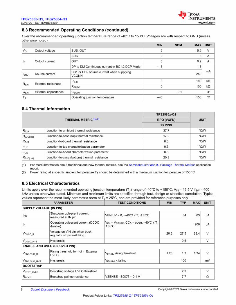
8.3 Recommended Operating Conditions (continued)Over the recommended operating junction temperature range of -40°C to 150°C. Voltages are with respect to GND (unless otherwise noted)
MIN NOM MAX UNITVO Output voltage BUS, OUT 5 5.5 V
IO Output current
BUS 0 3 A
OUT 0 0.2 A
DP to DM Continuous current in BC1.2 DCP Mode –15 15mA
ISRC Source current CC1 or CC2 source current when supplying VCONN 250
REXT External resistnaceRILIM 0 100 kΩ
RFREQ 0 100 kΩ
CEXT External capacitance CBOOT 0.1 uF
TJ Operating junction temperature –40 150 °C
8.4 Thermal Information
THERMAL METRIC(1) (2)
TPS2585x-Q1UNITRPQ (VQFN)
25 PINSRθJA Junction-to-ambient thermal resistance 37.7 °C/W
RθJC(top) Junction-to-case (top) thermal resistance 17.2 °C/W
RθJB Junction-to-board thermal resistance 8.8 °C/W
ΨJT Junction-to-top characterization parameter 0.3 °C/W
ΨJB Junction-to-board characterization parameter 8.8 °C/W
RθJC(bot) Junction-to-case (bottom) thermal resistance 20.3 °C/W
(1) For more information about traditional and new thermal metrics, see the Semiconductor and IC Package Thermal Metrics application report.
(2) Power rating at a specific ambient temperature TA should be determined with a maximum junction temperature of 150 °C.
8.5 Electrical Characteristics Limits apply over the recommended operating junction temperature (TJ) range of -40°C to +150°C; VIN = 13.5 V, fSW = 400 kHz unless otherwise stated. Minimum and maximum limits are specified through test, design or statistical correlation. Typical values represent the most likely parametric norm at TJ = 25°C, and are provided for reference purposes only.
PARAMETER TEST CONDITIONS MIN TYP MAX UNITSUPPLY VOLTAGE (IN PIN)
ISDShutdown quiescent current; measured at IN pin. VEN/UV = 0, –40 ≤ TJ ≤ 85 34 63 uA
IQOperating quiescent current (DCDC disable)
VEN = VSENSE, CCx = open, –40 ≤ TJ ≤ 85 200 µA
VOVLO_RVoltage on VIN pin when buck regulator stops switching 26.6 27.5 28.4 V
VOVLO_HYS Hysteresis 0.5 V
ENABLE AND UVLO (EN/UVLO PIN)
VEN/UVLO_RRising threshold for not in External UVLO VEN/UV rising threshold 1.26 1.3 1.34 V
VEN/UVLO_HYS Hysteresis VEN/UVLO falling 100 mV
BOOTSTRAPVBTST_UVLO Bootstrap voltage UVLO threshold 2.2 V
RBOOT Bootstrap pull-up resistence VSENSE - BOOT = 0.1 V 7.7 Ω
TPS25855-Q1, TPS25854-Q1SLVSFJ9 – SEPTEMBER 2021 www.ti.com
8 Submit Document Feedback Copyright © 2021 Texas Instruments Incorporated
Product Folder Links: TPS25855-Q1 TPS25854-Q1
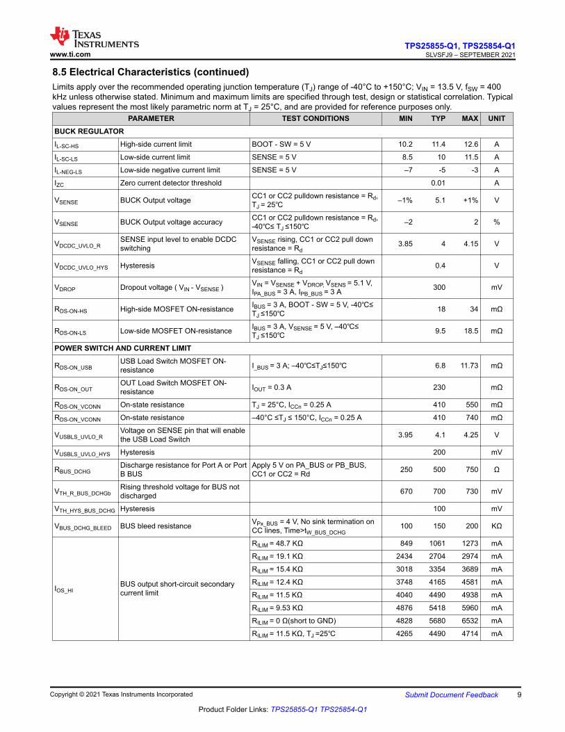
8.5 Electrical Characteristics (continued)Limits apply over the recommended operating junction temperature (TJ) range of -40°C to +150°C; VIN = 13.5 V, fSW = 400 kHz unless otherwise stated. Minimum and maximum limits are specified through test, design or statistical correlation. Typical values represent the most likely parametric norm at TJ = 25°C, and are provided for reference purposes only.
PARAMETER TEST CONDITIONS MIN TYP MAX UNITBUCK REGULATORIL-SC-HS High-side current limit BOOT - SW = 5 V 10.2 11.4 12.6 A
IL-SC-LS Low-side current limit SENSE = 5 V 8.5 10 11.5 A
IL-NEG-LS Low-side negative current limit SENSE = 5 V –7 -5 -3 A
IZC Zero current detector threshold 0.01 A
VSENSE BUCK Output voltage CC1 or CC2 pulldown resistance = Rd, TJ = 25 –1% 5.1 +1% V
VSENSE BUCK Output voltage accuracy CC1 or CC2 pulldown resistance = Rd, -40≤ TJ ≤150 –2 2 %
VDCDC_UVLO_RSENSE input level to enable DCDC switching
VSENSE rising, CC1 or CC2 pull down resistance = Rd
3.85 4 4.15 V
VDCDC_UVLO_HYS Hysteresis VSENSE falling, CC1 or CC2 pull down resistance = Rd
0.4 V
VDROP Dropout voltage ( VIN - VSENSE )VIN = VSENSE + VDROP, VSENS = 5.1 V, IPA_BUS = 3 A, IPB_BUS = 3 A 300 mV
RDS-ON-HS High-side MOSFET ON-resistance IBUS = 3 A, BOOT - SW = 5 V, -40≤ TJ ≤150 18 34 mΩ
RDS-ON-LS Low-side MOSFET ON-resistance IBUS = 3 A, VSENSE = 5 V, –40≤ TJ ≤150 9.5 18.5 mΩ
POWER SWITCH AND CURRENT LIMIT
RDS-ON_USBUSB Load Switch MOSFET ON-resistance I_BUS = 3 A; –40≤TJ≤150 6.8 11.73 mΩ
RDS-ON_OUTOUT Load Switch MOSFET ON-resistance IOUT = 0.3 A 230 mΩ
RDS-ON_VCONN On-state resistance TJ = 25°C, ICCn = 0.25 A 410 550 mΩ
RDS-ON_VCONN On-state resistance –40°C ≤TJ ≤ 150°C, ICCn = 0.25 A 410 740 mΩ
VUSBLS_UVLO_RVoltage on SENSE pin that will enable the USB Load Switch 3.95 4.1 4.25 V
VUSBLS_UVLO_HYS Hysteresis 200 mV
RBUS_DCHGDischarge resistance for Port A or Port B BUS
Apply 5 V on PA_BUS or PB_BUS, CC1 or CC2 = Rd 250 500 750 Ω
VTH_R_BUS_DCHGbRising threshold voltage for BUS not discharged 670 700 730 mV
VTH_HYS_BUS_DCHG Hysteresis 100 mV
VBUS_DCHG_BLEED BUS bleed resistance VPx_BUS = 4 V, No sink termination on CC lines, Time>tW_BUS_DCHG
100 150 200 KΩ
IOS_HIBUS output short-circuit secondary current limit
RILIM = 48.7 KΩ 849 1061 1273 mA
RILIM = 19.1 KΩ 2434 2704 2974 mA
RILIM = 15.4 KΩ 3018 3354 3689 mA
RILIM = 12.4 KΩ 3748 4165 4581 mA
RILIM = 11.5 KΩ 4040 4490 4938 mA
RILIM = 9.53 KΩ 4876 5418 5960 mA
RILIM = 0 Ω(short to GND) 4828 5680 6532 mA
RILIM = 11.5 KΩ, TJ =25 4265 4490 4714 mA
www.ti.comTPS25855-Q1, TPS25854-Q1
SLVSFJ9 – SEPTEMBER 2021
Copyright © 2021 Texas Instruments Incorporated Submit Document Feedback 9
Product Folder Links: TPS25855-Q1 TPS25854-Q1

8.5 Electrical Characteristics (continued)Limits apply over the recommended operating junction temperature (TJ) range of -40°C to +150°C; VIN = 13.5 V, fSW = 400 kHz unless otherwise stated. Minimum and maximum limits are specified through test, design or statistical correlation. Typical values represent the most likely parametric norm at TJ = 25°C, and are provided for reference purposes only.
PARAMETER TEST CONDITIONS MIN TYP MAX UNIT
IOS_BUS BUS output short-circuit current limit
RILIM = 48.7 KΩ 530.4 663 800 mA
RILIM = 19.1 KΩ 1521 1690 1859 mA
RILIM = 15.4 KΩ 1886.4 2096 2305.6 mA
RILIM = 12.4 KΩ 2342.7 2603 2863.3 mA
RILIM = 11.5 KΩ 2525.4 2806 3086.6 mA
RILIM = 9.53 KΩ 3047.4 3386 3724.6 mA
RILIM = 0 Ω(short to GND) 3017.5 3550 4082.5 mA
RILIM =11.5 KΩ, TJ =25 2666 2806 2946 mA
IOS_OUT OUT output short-circuit current limit Short circuit current limit 390 450 495 mA
IOS_VCONNVCONN output short-circuit current limit Short circuit current limit 240 300 360 mA
CABLE COMPENSATION VOLTAGE
VDROP_COM Cable compensation voltage
IBUS=2.4A, RIMON=0Ω 0 mV
IBUS=2.4A, RIMON=0.976KΩ 39.5 mV
IBUS=2.4A, RIMON=2.94KΩ 119.2 mV
IBUS=2.4A, RIMON=4.99KΩ 202.4 mV
IBUS=2.4A, RIMON=6.98KΩ 283.1 mV
IBUS=2.4A, RIMON=8.87KΩ 360 mV
IBUS=2.4A, RIMON=9.76KΩ 396 mV
CC CONNECT MANAGEMENTISRC_CC_3A Sourcing current CC pin voltage: 0 V ≤ VCCn ≤ 2.45 V 304 330 356 µA
ISRC_CC_1.5ASourcing current in thermal management(Temp warm)
CC pin voltage: 0 V ≤ VCCn ≤ 1.5 V , TA> 85 167 180 194 µA
ISRC_CC_DFLTSourcing current in thermal management(Temp hot)
CC pin voltage: 0 V ≤ VCCn ≤ 1.5 V , TA> 85 64 80 105 µA
IREV Reverse leakage current
CCx is the CC pin under test, CCy is the other CC pin. CC pin voltage VCCx = 5.5 V, CCy floating, VEN_UV = 0 V or VSENSE, 0 V ≤ VIN ≤ 26 V IREV is current into CCx pin
2.75 10 µA
VTH_RRising threshold voltage for VCONN not discharged
CC pin that was providing VCONN in previous SINK state 670 700 730 mV
VTH_HYS Hysteresis 100 mV
FAULT, POL, THERM_WARNVOL FAULT Output low voltage ISNK_PIN = 1 mA 250 mV
IOFF FAULT Off-state leakage VPIN = 5.5 V 2.2 µA
VOL POL Output low voltage ISNK_PIN = 1 mA 250 mV
IOFF POL Off-state leakage VPIN = 5.5 V 1.8 µA
VOL THERM_WARN Output low voltage ISNK_PIN = 1 mA 250 mV
IOFF THERM_WARN Off-state leakage VPIN = 5.5 V 10 µA
BC 1.2 DOWNSTREAM CHARGING PORTRDPM_SHORT DP and DM shorting resistance 70 200 Ω
DIVIDER 3 MODEVDP_DIV3 DP output voltage 2.57 2.7 2.84 V
VDM_DIV3 DM output voltage 2.57 2.7 2.84 V
TPS25855-Q1, TPS25854-Q1SLVSFJ9 – SEPTEMBER 2021 www.ti.com
10 Submit Document Feedback Copyright © 2021 Texas Instruments Incorporated
Product Folder Links: TPS25855-Q1 TPS25854-Q1

8.5 Electrical Characteristics (continued)Limits apply over the recommended operating junction temperature (TJ) range of -40°C to +150°C; VIN = 13.5 V, fSW = 400 kHz unless otherwise stated. Minimum and maximum limits are specified through test, design or statistical correlation. Typical values represent the most likely parametric norm at TJ = 25°C, and are provided for reference purposes only.
PARAMETER TEST CONDITIONS MIN TYP MAX UNITRDP_DIV3 DP output impedance IDP_IN = –5 µA 24 30 36 kΩ
RDM_DIV3 DM output impedance IDM_IN = –5 µA 24 30 36 kΩ
1.2-V MODEVDP_1.2V DP output voltage 1.12 1.2 1.26 V
VDM_1.2V DM output voltage 1.12 1.2 1.26 V
RDP_1.2V DP output impedance IDP_IN = –5 µA 84 100 126 kΩ
RDM_1.2V DM output impedance IDM_IN = –5 µA 84 100 126 kΩ
FREQ/SYNC THRESHOLD
VIH_FREQ/SYNCFREQ/SYNC high threshold for external clock synchronization
Amplitude of SYNC clock AC signal (measured at FREQ/SYNC pin) 2 V
VIL_FREQ/SYNCFREQ/SYNC low threshold for external clock synchronization
Amplitude of SYNC clock AC signal (measured at FREQ/SYNC pin) 0.8 V
TEMPERATURE SENSINGVWARN_HIGH Temperature warning threshold rising As percentage to VSENSE 0.475 0.5 0.525 V/V
VWARN_HYS Hysteresis As percentage to VSENSE 0.1 V/V
VHOT_HIGHTemperature Hot assert threshold rising to reduce SENS voltage As percentage to VSENSE 0.618 0.65 0.683 V/V
VHOT_HYS Hysteresis As percentage to VSENSE 0.1 V/V
VR_VSENSVSENSE voltage decay when Temperature Hot assert
TS pin voltage rise above 0.65 * VSENSE
4.77 V
THERMAL SHUTDOWN
TLS_SD USB Load Switch Over TemperatureShutdown threshold 160 °C
Recovery threshold 150 °C
TSD Thermal shutdownShutdown threshold 166 °C
Recovery threshold 154 °C
8.6 Timing Requirements Over the recommended operating junction temperature range of -40 °C to 150 °C (unless otherwise noted)
MIN NOM MAX UNIT
tDEGLA_FAULT Asserting deglitch time (Thermal SD Fault assertion is instantaneous, not subject to this timing) 2.94 4.1 5.42 ms
tDEGLD_FAULT De-asserting deglitch time 11.09 16.38 23.03 ms
BUS DISCHARGEtDEGA_BUS_DCHG
Discharge asserting deglitch 5.6 12.3 21.2 ms
tW_BUS_DCHGVBUS discharge time after sink termination removed from CC lines
VBUS = 1 V, time ISNK_OUT > 1 mA after sink termination removed from CC lines 170 260 360 ms
POWER SWITCH TIMING
tIOS_HI_DEGDeglitch time for USB power switch current limit enable USB port enter overcurrent (per ILIM setting) 1.228 2.048 2.867 ms
tIOS_HI_RST MFI OCP reset timing 9.6 16 22.4 ms
tr_USB PA_BUS, PB_BUS voltage rise time CL = 1 µF, RL = 100 Ω (measured from 10% to 90% of final value) 1.67 ms
tf_USB PA_BUS, PB_BUS voltage fall time CL = 1 µF, RL = 100 Ω (measured from 90% to 10% of final value) 0.49 ms
ton_USB PA_BUS, PB_BUS voltage turnon-time CL = 1 µF, RL = 100 Ω 2.59 ms
www.ti.comTPS25855-Q1, TPS25854-Q1
SLVSFJ9 – SEPTEMBER 2021
Copyright © 2021 Texas Instruments Incorporated Submit Document Feedback 11
Product Folder Links: TPS25855-Q1 TPS25854-Q1

8.6 Timing Requirements (continued)Over the recommended operating junction temperature range of -40 °C to 150 °C (unless otherwise noted)
MIN NOM MAX UNITtoff_USB PA_BUS, PB_BUS voltage turnoff-time CL = 1 µF, RL = 100 Ω 2.07 ms
tIOS_USBPA_BUS, PB_BUS short-circuit response time CL = 1 µF, RL = 1 Ω 1 us
tr_OUT OUT voltage rise time CL = 1 µF, RL = 100 Ω (measured from 10% to 90% of final value) 0.12 0.2 0.28 ms
tf_OUT OUT voltage fall time CL = 1 µF, RL = 100 Ω (measured from 90% to 10% of final value) 0.16 0.22 0.28 ms
ton_OUT OUT voltage turnon-time CL = 1 µF, RL = 100 Ω 0.6 1.1 1.65 ms
toff_OUT OUT voltage turnoff-time CL = 1 µF, RL = 100 Ω 0.45 0.54 0.62 ms
tIOS_OUT OUT short-circuit response time CL = 1 µF, RL = 1 Ω 1.4 4 us
tIOS_VCONN CC-VCONN short circuit response time CL = 1 µF, RL = 1 Ω 1 3.5 µs
tr_VCONN VCONN output voltage rise timeCL = 1 µF, RL = 100 Ω (measured from 10% to 90% of final value); 5.1KΩ on CC1 and 1KΩ on CC2
0.2 0.28 0.36 ms
tf_VCONN VCONN output voltage fall timeCL = 1 µF, RL = 100 Ω (measured from 90% to 10% of final value); 5.1KΩ on CC1 and 1KΩ on CC2
0.18 0.23 0.28 ms
ton_VCONN VCONN output voltage turnon time CL = 1 µF, RL = 100 Ω; 5.1KΩ on CC1 and 1KΩ on CC2 0.7 1.2 1.7 ms
toff_VCONN VCONN output voltage turnoff time CL = 1 µF, RL = 100 Ω; 5.1KΩ on CC1 and 1KΩ on CC2 0.37 0.44 0.51 ms
HICCUP MODE
THICP_ONOUT, PA_BUS, PB_BUS output hiccup mode ON time OC, VOUT, VPA_BUS, VPB_BUS drop 10% 2.94 4.1 5.42 ms
THICP_OFFOUT, PA_BUS, PB_BUS output hiccup mode OFF time
OC, OUT, PA_BUS, PB_BUS connect to GND 367 524 715 ms
8.7 Switching Characteristics Over the recommended operating junction temperature range of -40 °C to 150 °C (unless otherwise noted)
PARAMETER TEST CONDITIONS MIN TYP MAX UNITSW (SW PIN)TON_MIN Minimum turnon-time 84 ns
TON_MAXMaximum turnon-time, HS timeout in dropout 6 µs
TOFF_MIN Minimum turnoff time 81 ns
Dmax Maximum switch duty cycle 98 %
TIMING RESISTOR AND INTERNAL CLOCK
fSW_RANGESwitching frequency range using FREQ mode (TPS25854-Q1) 9 kΩ ≤ RFREQ≤ 99 kΩ 200 800 kHz
fSW_RANGESwitching frequency range using FREQ mode (TPS25855-Q1) 9 kΩ ≤ RFREQ≤ 99 kΩ 200 3000 kHz
fSW Switching frequencyRFREQ = 80.6 kΩ 228 253 278 kHz
RFREQ = 49.9 kΩ 360 400 440 kHz
fSW Switching frequency (TPS25855-Q1) RFREQ = 8.45 kΩ 1980 2200 2420 kHz
FSSSFrequency span of spread spectrum operation ±6 %
EXTERNAL CLOCK(SYNC)
TPS25855-Q1, TPS25854-Q1SLVSFJ9 – SEPTEMBER 2021 www.ti.com
12 Submit Document Feedback Copyright © 2021 Texas Instruments Incorporated
Product Folder Links: TPS25855-Q1 TPS25854-Q1

8.7 Switching Characteristics (continued)Over the recommended operating junction temperature range of -40 °C to 150 °C (unless otherwise noted)
PARAMETER TEST CONDITIONS MIN TYP MAX UNIT
fFREQ/SYNC
Switching frequency using external clock on FREQ/SYNC pin (TPS25854-Q1)
200 800 kHz
fFREQ/SYNC
Switching frequency using external clock on FREQ/SYNC pin (TPS25855-Q1)
200 3000 kHz
TSYNC_MIN Minimum SYNC input pulse widthfSYNC = 400kHz, VFREQ/SYNC > VIH_FREQ/SYNC, VFREQ/SYNC < VIL_FREQ/SYNC
100 ns
TLOCK_IN PLL lock time 100 µs
CC - CONNECT MANAGEMENT - ATTACH AND DETACH DEGLITCH
tDEGA_CC_ATT_DETMAttach asserting deglitch in the Detached Mode 1.29 2.05 3.05 ms
Attach asserting deglitch in the Detached Mode Fast clock test mode 128 µs
tDEGA_CC_DETACH_SINKM
Detach asserting deglitch for exiting SINK Mode 8.2 12.5 18 ms
Detach asserting deglitch for exiting SINK Mode Fast clock test mode 0.96 ms
tDEGA_CC_SHORT Detach, Rd and Ra asserting deglitch 92 192 339 µs
tDEGA_CC_LONG Long deglitch 103 148 200 ms
Long deglitch Fast clock test mode 288 us
www.ti.comTPS25855-Q1, TPS25854-Q1
SLVSFJ9 – SEPTEMBER 2021
Copyright © 2021 Texas Instruments Incorporated Submit Document Feedback 13
Product Folder Links: TPS25855-Q1 TPS25854-Q1

8.8 Typical CharacteristicsUnless otherwise specified the following conditions apply: VIN = 13.5 V, fSW = 2.1 MHz, L = 2.2 µH, CSENSE = 66 µF, C_BUS = 1 µF, TA = 25 °C.
Input Voltage (V)
Sh
utd
ow
n Q
uie
scen
t C
urr
ent
(uA
)
4 8 12 16 20 24 28 3220
30
40
50
60
70-40C25C150C
VEN/EULVO = 0 V CC1 = Rd
Figure 8-1. Shutdown Quiescent Current
Input Voltage (V)
Sta
nd
by Q
ue
iscen
t C
urr
en
t (u
A)
4 8 12 16 20 24 28 32100
120
140
160
180
200-40C25C150C
VEN/UVLO = VSENSE CC1/2 = OPEN
Figure 8-2. Standby Quiescent Current
Temperature (C)
EN
Thre
sho
ld V
otla
ge (
V)
-50 -25 0 25 50 75 100 125 1501.26
1.28
1.3
1.32
1.34
1.36Vin = 5.5VVin = 13.5VVin = 26V
Figure 8-3. Precision Device Enable ThresholdTemperature (C)
VSEN
SE V
olta
ge (V
)
-50 -25 0 25 50 75 100 125 1505.07
5.08
5.09
5.1
5.11
5.12
5.13Vin = 5.5VVin = 13.5VVin = 26V
Figure 8-4. VSENSE Voltage vs Junction Temperature
Temperature (C)
DC
DC
UV
LO
Volta
ge
(V
)
-50 -25 0 25 50 75 100 125 1504.06
4.04
4.02
4
3.98
3.96
3.94Vin = 5.5VVin = 13.5VVin = 26V
VEN/EULVO = VSENSE CC1= Rd
Figure 8-5. DCDC UVLO Threshold
Input Voltage (V)
Hig
h-s
ide
MO
S C
urr
ent
Lim
it (
A)
4 8 12 16 20 24 2811.2
11.3
11.4
11.5
11.6
11.7-40C25C150C
Figure 8-6. High-side Current Limit vs Input Voltage
TPS25855-Q1, TPS25854-Q1SLVSFJ9 – SEPTEMBER 2021 www.ti.com
14 Submit Document Feedback Copyright © 2021 Texas Instruments Incorporated
Product Folder Links: TPS25855-Q1 TPS25854-Q1

8.8 Typical Characteristics (continued)Unless otherwise specified the following conditions apply: VIN = 13.5 V, fSW = 2.1 MHz, L = 2.2 µH, CSENSE = 66 µF, C_BUS = 1 µF, TA = 25 °C.
Input Voltage (V)
Low
-sid
e M
OS
Curr
en
t L
imit (
A)
4 8 12 16 20 24 289.8
9.9
10
10.1
10.2
10.3-40C25C150C
Figure 8-7. Low-side Current Limit vs Input VoltageTemperature (C)
On
Re
sis
tan
ce
(m:
)
-50 -25 0 25 50 75 100 125 15015
20
25
30
35
40Vin = 5.5VVin = 13.5VVin = 26V
I_BUS = 3 A
Figure 8-8. High-side MOSFET on Resistance vs Junction Temperature
Temperature (C)
On
Re
sis
tan
ce
(m:
)
-50 -25 0 25 50 75 100 125 1508
10
12
14
16
18
Vin = 5.5VVin = 13.5VVin = 26V
IBUS = 3 A
Figure 8-9. Low-side MOSFET on Resistance vs Junction Temperature
Temperature (C)
US
B P
ow
er
Sw
itch
Cu
rren
t L
imit (
mA
)
-50 -25 0 25 50 75 100 125 1503400
3440
3480
3520
3560
3600
3640Vin = 5.5VVin = 13.5VVin = 26V
ILIM = GND
Figure 8-10. USB Power Switch Current Limit vs Junction Temperature
Temperature (C)
US
B P
ow
er
Sw
itch
Cu
rren
t L
imit (
mA
)
-50 -25 0 25 50 75 100 125 1503280
3320
3360
3400
3440
3480
3520Vin = 5.5VVin = 13.5VVin = 26V
RILIM = 9.53 kΩ
Figure 8-11. USB Power Switch Current Limit vs Junction Temperature
Temperature (C)
US
B P
ow
er
Sw
itch
Cu
rren
t L
imit (
mA
)
-50 -25 0 25 50 75 100 125 1501960
2000
2040
2080
2120
2160
2200Vin = 5.5VVin = 13.5VVin = 26V
RILIM = 15.4 kΩ
Figure 8-12. USB Power Switch Current Limit vs Junction Temperature
www.ti.comTPS25855-Q1, TPS25854-Q1
SLVSFJ9 – SEPTEMBER 2021
Copyright © 2021 Texas Instruments Incorporated Submit Document Feedback 15
Product Folder Links: TPS25855-Q1 TPS25854-Q1

8.8 Typical Characteristics (continued)Unless otherwise specified the following conditions apply: VIN = 13.5 V, fSW = 2.1 MHz, L = 2.2 µH, CSENSE = 66 µF, C_BUS = 1 µF, TA = 25 °C.
Temperature (C)
OU
T P
ow
er
Sw
itch
Cu
rre
nt L
imit (
mA
)
-50 -25 0 25 50 75 100 125 150400
420
440
460
480
500
520Vin = 5.5VVin = 13.5VVin = 26V
Figure 8-13. OUT Power Switch Current Limit vs Junction Temperature
Temperature (C)
VC
ON
N P
ow
er
Sw
itch
Cu
rre
nt L
imit (
mA
)
-50 -25 0 25 50 75 100 125 150280
288
296
304
312
320
328Vin = 5.5VVin = 13.5VVin = 26V
Figure 8-14. VCONN Power Switch Current Limit vs Junction Temperature
Temperature (C)
Ca
ble
Co
mp
Vo
lta
ge (
V)
-50 -25 0 25 50 75 100 125 15080
84
88
92
96
100
IBUS = 2.4 A RIMON=2.21 kΩ
Figure 8-15. Cable Compensation Voltage vs Junction Temperature
Temperature (C)
On
Re
sis
tan
ce
(m:
)
-50 -25 0 25 50 75 100 125 1504.8
5.6
6.4
7.2
8
8.8
9.6
Vin = 5.5VVin = 13.5VVin = 26V
Figure 8-16. USB Power Switch On Resistance vs Junction Temperature
Temperature (C)
On
Re
sis
tan
ce
(m:
)
-50 -25 0 25 50 75 100 125 150160
200
240
280
320
360
400Vin = 5.5VVin = 13.5VVin = 26V
Figure 8-17. OUT Power Switch On Resistance vs Junction Temperature
Temperature (C)
On
Re
sis
tan
ce
(m:
)
-50 -25 0 25 50 75 100 125 150300
350
400
450
500
550
600
Vin = 5.5VVin = 13.5VVin = 26V
Figure 8-18. VCONN Power Switch On Resistance vs Junction Temperature
TPS25855-Q1, TPS25854-Q1SLVSFJ9 – SEPTEMBER 2021 www.ti.com
16 Submit Document Feedback Copyright © 2021 Texas Instruments Incorporated
Product Folder Links: TPS25855-Q1 TPS25854-Q1

8.8 Typical Characteristics (continued)Unless otherwise specified the following conditions apply: VIN = 13.5 V, fSW = 2.1 MHz, L = 2.2 µH, CSENSE = 66 µF, C_BUS = 1 µF, TA = 25 °C.
Temperature (C)
Sw
itch
ing
Fre
qu
en
cy (
kH
z)
-50 -25 0 25 50 75 100 125 150376
384
392
400
408
416
424Vin = 5.5VVin = 13.5VVin = 26V
RFREQ = 49.9 kΩ
Figure 8-19. Switching Frequency vs Junction Temperature
Temperature (C)
Sw
itch
ing
Fre
qu
en
cy (
kH
z)
-50 -25 0 25 50 75 100 125 1502040
2080
2120
2160
2200
2240
2280Vin = 5.5VVin = 13.5VVin = 26V
RFREQ = 8.45 kΩ
Figure 8-20. Switching Frequency vs Junction Temperature
Temperature (C)
So
urc
ing C
urr
ent
(uA
)
-50 -25 0 25 50 75 100 125 150150
200
250
300
350
400
450UFP 1.5AUFP 3A
Figure 8-21. CC Sourcing Current vs Junction TemperatureTemperature (C)
TC
Tem
p W
arn
ing T
hre
sh
old
(%
)
-50 -25 0 25 50 75 100 125 1500.44
0.46
0.48
0.5
0.52
0.54
0.56
Figure 8-22. TS Temperature Wam Threshold vs Junction Temperature
Temperature (C)
TC
Tem
p H
ot T
hre
sho
ld (
%)
-50 -25 0 25 50 75 100 125 1500.6
0.62
0.64
0.66
0.68
0.7
0.72
Figure 8-23. TS Temperature Hot Threshold vs Junction Temperature
Temperature (C)
VS
EN
SE V
olta
ge
in
Te
mp
Ho
t (V
)
-50 -25 0 25 50 75 100 125 1504.7
4.72
4.74
4.76
4.78
4.8
4.82
Figure 8-24. SENSE Voltage in Temperature Hot vs Junction Temperature
www.ti.comTPS25855-Q1, TPS25854-Q1
SLVSFJ9 – SEPTEMBER 2021
Copyright © 2021 Texas Instruments Incorporated Submit Document Feedback 17
Product Folder Links: TPS25855-Q1 TPS25854-Q1

9 Parameter Measurement Information
OUT
R(L) C(L)
Figure 9-1. OUT Rise-Fall Test Load Figure
tftr
10%
90%
V(OUT)
Figure 9-2. Power-On and -Off Timing
5 V
0 V
V(OU T)
t(DCHG)
Figure 9-3. OUT Discharge During Mode Change
V(EN)
V(OUT)
ton toff
50% 50%
10%
90%
Figure 9-4. Enable Timing, Active-High Enable
t(IOS)
IOS
I(OUT)
Figure 9-5. Output Short-Circuit Parameters
TPS25855-Q1, TPS25854-Q1SLVSFJ9 – SEPTEMBER 2021 www.ti.com
18 Submit Document Feedback Copyright © 2021 Texas Instruments Incorporated
Product Folder Links: TPS25855-Q1 TPS25854-Q1

10 Detailed Description10.1 OverviewThe TPS2585x-Q1 is full-featured solution for implementing a compact USB charging port with support for both Type-C and BC1.2 standards. Both devices contain an efficient buck regulator power source. For single Type-C port, the TPS2585x-Q1 is capable of providing 3.4 A of output current at 5.1 V (nominal), which is 3 A for Type-C port, 200 mA for OUT pin, and 200 mA for VCONN power. The TPS2585x-Q1 is an automotive-focused USB charging controller, to offer a robust solution, TI recommends to add adequate protection (TVS3300 equivalent or better but auto quality) on IN pin to protect systems from high power transients or lightning strikes.
System designers can optimize efficiency or solution size through careful selection of switching frequency in the range of 200 kHz–2400 kHz with sufficient margin to operate above or below the AM radio frequency band. TPS2585x-Q1 protects itself with internal thermal sensing circuits that monitor the operating temperature of the junction and disables operation if the temperature exceeds the Thermal Shutdown threshold, so in high ambient temperature application, the 3.4-A output current capability is not assured. In the TPS2585x-Q1, the buck regulator operates in forced PWM mode, ensuring fixed switching frequency regardless of load current. Spread-spectrum frequency dithering reduces harmonic peaks of the switching frequency, potentially simplifying EMI filter design and easing compliance.
Current sensing through a precision FET current sense amplifier on USB port enables an accurate, user programmable over-current limit setting, and programmable linear cable compensation to overcome IR losses when powering remote USB ports.
TPS2585x-Q1 includes a TS input for user programmable thermal protection using a negative temperature coefficient (NTC) resistor. The TPS25855-Q1 has THERM_WARN flag to indicate the NTC temperature is warm before it enters the temperature hot range.
Both devices can support the USB Type-C protocol, and also support the legacy Battery Charging Specification Rev 1.2 (BC1.2) DCP mode with auto-detect feature to charge not only BC1.2 compliant hand-held devices but also popular phones and tablets that incorporate their own propriety charging algorithm. The TPS2585x-Q1 also supports USB cable polarity detection and fault condition detection.
www.ti.comTPS25855-Q1, TPS25854-Q1
SLVSFJ9 – SEPTEMBER 2021
Copyright © 2021 Texas Instruments Incorporated Submit Document Feedback 19
Product Folder Links: TPS25855-Q1 TPS25854-Q1

10.2 Functional Block Diagram
TPS25855-Q1, TPS25854-Q1SLVSFJ9 – SEPTEMBER 2021 www.ti.com
20 Submit Document Feedback Copyright © 2021 Texas Instruments Incorporated
Product Folder Links: TPS25855-Q1 TPS25854-Q1

10.3 Feature Description10.3.1 Power Down or Undervoltage Lockout
The device is in power down mode if the IN terminal voltage is less than VUVLO. The part is considered dead and all the terminals are high impedance. Once the IN voltage rises above the VUVLO threshold, the IC enters sleep mode or active mode depending on the EN/UVLO voltage.
The voltage on the EN/UVLO pin controls the ON/OFF operation of TPS2585x-Q1. An EN/UVLO pin voltage higher than VEN/UVLO-H is required to start the internal regulator and begin monitoring the CCn lines for a valid Type-C connection. The internal USB monitoring circuitry is on when VIN is within the operation range and the EN/UVLO threshold is cleared. The buck regulator starts to operate, however, the USB ports load switch remain OFF until a valid Type-C detection has been made. This feature ensures the cold socket (0 V) USB Type-C VBUS requirement is met.
The EN/UVLO pin is an input and cannot be left open or floating. The simplest way to enable the operation of the TPS2585x-Q1 is to connect the EN to SENSE. This connection allows self-start-up of the TPS2585x-Q1 when VIN is within the operation range. Note that cannot connect the EN to IN pin directly for self-start-up.
Many applications benefit from the employment of an enable divider RENT and RENB to establish a precision system UVLO level for the TPS2585x-Q1, shown in Figure 10-1. The system UVLO can be used for sequencing, ensuring reliable operation, or supply protection, such as a battery discharge level. To ensure the USB ports VBUS is within the 5-V operating range as required for USB compliance (for the latest USB specifications and requirements, refer to USB.org), TI suggests that the RENT and RENB resistors be chosen such that the TPS2585x-Q1 enables when VIN is approximately 6 V. Considering the drop out voltage of the buck regulator and IR loses in the system, 6 V provides adequate margin to maintain VBUS within USB specifications. If system requirements such as a warm crank (start) automotive scenario require operation with VIN < 6 V, the values of RENT and RENB can be calculated assuming a lower VIN. An external logic signal can also be used to drive EN/UVLO input when a microcontroller is present and it is desirable to enable or disable the USB port remotely for other reasons.
RENB
EN
IN
RENT
Figure 10-1. System UVLO by Enable Divider
UVLO configuration using external resistors is governed by the following equations:
(1)
(2)
Example:
VIN(ON) = 6V
RENT = 20 kΩ
www.ti.comTPS25855-Q1, TPS25854-Q1
SLVSFJ9 – SEPTEMBER 2021
Copyright © 2021 Texas Instruments Incorporated Submit Document Feedback 21
Product Folder Links: TPS25855-Q1 TPS25854-Q1

RENB = [(VEN-VOUT-H) / (VIN(ON) – VEN)] × RENT (3)
RENB = 5 kΩ
Therefore VIN(OFF) = 5.5 V
10.3.2 Input Overvoltage Protection (OVP) - Continuously Monitored
The operation voltage range for TPS2585x-Q1 is up to 26 V. If the input source applies an overvoltage, the buck regulator HSFET/LSFET turns off immediately. Thus, the USB ports and OUT pin loses their power as well. Once the overvoltage returns to a normal voltage, the buck regulator continues switching and provide power on the USB ports and OUT pin.
During the overvoltage condition, the internal regulator regulates the SENSE voltage at 5 V, so the SENSE always has power for internal bias circuit and external NTC pull-up reference.
10.3.3 Buck Converter
The following operating description of the TPS2585x-Q1 refers to the Functional Block Diagram. The TPS2585x-Q1 integrates a monolithic, synchronous, rectified, step-down, switch-mode converter with internal power MOSFETs and USB current-limit switches with charging ports auto-detection. The TPS2585x-Q1 offers a compact and high efficiency solution with excellent load and line regulation over a wide input supply range. The TPS2585x-Q1 supplies a regulated output voltage by turning on the high-side (HS) and low-side (LS) NMOS switches with controlled duty cycle. During high-side switch ON time, the SW pin voltage swings up to approximately VIN, and the inductor current, iL, increase with linear slope (VIN – VOUT ) / L. When the HS switch is turned off by the control logic, the LS switch is turned on after an anti-shoot-through dead time. Inductor current discharges through the LS switch with a slope of –VOUT / L. The control parameter of a buck converter is defined as Duty Cycle D = tON / TSW, where tON is the high-side switch ON time and TSW is the switching period, shown in Figure 10-2. The regulator control loop maintains a constant output voltage by adjusting the duty cycle D. In an ideal buck converter, where losses are ignored, D is proportional to the output voltage and inversely proportional to the input voltage: D = VOUT / VIN.
VSW
VIN
D = tON/ TSW
tON tOFF
TSW
t
-VD
0
SW
Vo
lta
ge
iL
IOUT
t0
Ind
ucto
r C
urr
en
t
ILPK
'iL
Figure 10-2. SW Node and Inductor Current Waveforms in Continuous Conduction Mode (CCM)
The TPS2585x-Q1 operates in a fixed-frequency, peak-current-mode control to regulate the output voltage. A voltage feedback loop is used to get accurate DC voltage regulation by adjusting the peak current command based on voltage offset. The peak inductor current is sensed from the high-side switch and compared to the peak current threshold to control the ON time of the high-side switch. The voltage feedback loop is internally compensated, which allows for fewer external components, makes it easy to design, and provides stable operation with a reasonable combination of output capacitors. TPS2585x-Q1 operates in FPWM mode for low output voltage ripple, tight output voltage regulation, and constant switching frequency.
TPS25855-Q1, TPS25854-Q1SLVSFJ9 – SEPTEMBER 2021 www.ti.com
22 Submit Document Feedback Copyright © 2021 Texas Instruments Incorporated
Product Folder Links: TPS25855-Q1 TPS25854-Q1
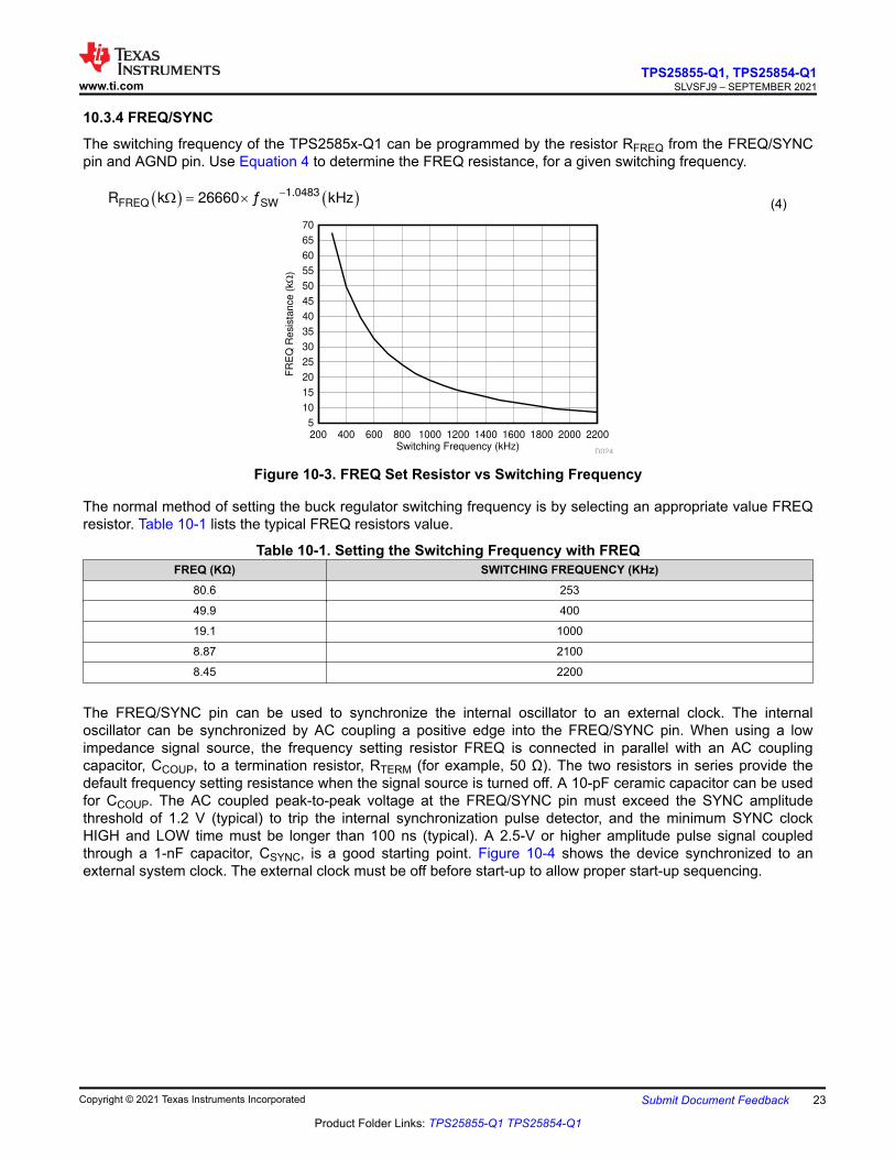
10.3.4 FREQ/SYNC
The switching frequency of the TPS2585x-Q1 can be programmed by the resistor RFREQ from the FREQ/SYNC pin and AGND pin. Use Equation 4 to determine the FREQ resistance, for a given switching frequency.
1.0483FREQ SWR k 26660 kHz¦ : u (4)
Switching Frequency (kHz)
FR
EQ
Resis
tance (
k:
)
200 400 600 800 1000 1200 1400 1600 1800 2000 22005
10
15
20
25
30
35
40
45
50
55
60
65
70
D024
Figure 10-3. FREQ Set Resistor vs Switching Frequency
The normal method of setting the buck regulator switching frequency is by selecting an appropriate value FREQ resistor. Table 10-1 lists the typical FREQ resistors value.
Table 10-1. Setting the Switching Frequency with FREQFREQ (KΩ) SWITCHING FREQUENCY (KHz)
80.6 253
49.9 400
19.1 1000
8.87 2100
8.45 2200
The FREQ/SYNC pin can be used to synchronize the internal oscillator to an external clock. The internal oscillator can be synchronized by AC coupling a positive edge into the FREQ/SYNC pin. When using a low impedance signal source, the frequency setting resistor FREQ is connected in parallel with an AC coupling capacitor, CCOUP, to a termination resistor, RTERM (for example, 50 Ω). The two resistors in series provide the default frequency setting resistance when the signal source is turned off. A 10-pF ceramic capacitor can be used for CCOUP. The AC coupled peak-to-peak voltage at the FREQ/SYNC pin must exceed the SYNC amplitude threshold of 1.2 V (typical) to trip the internal synchronization pulse detector, and the minimum SYNC clock HIGH and LOW time must be longer than 100 ns (typical). A 2.5-V or higher amplitude pulse signal coupled through a 1-nF capacitor, CSYNC, is a good starting point. Figure 10-4 shows the device synchronized to an external system clock. The external clock must be off before start-up to allow proper start-up sequencing.
www.ti.comTPS25855-Q1, TPS25854-Q1
SLVSFJ9 – SEPTEMBER 2021
Copyright © 2021 Texas Instruments Incorporated Submit Document Feedback 23
Product Folder Links: TPS25855-Q1 TPS25854-Q1

PLLRT
RTERM
Lo-Z
Clock
Source
FREQ/
SYNC
PLL
RT
Hi-Z
Clock
Source
FREQ/
SYNC
CCOUP
Figure 10-4. Synchronize to External Clock
The TPS25854-Q1 switching action can be synchronized to an external clock from 200 KHz to 800 KHz, and the TPS25855-Q1 switching action can be synchronized to an external clock from 200 KHz to 3 MHz. Even the switching frequency can be set to higher than 2.4 MHz, but TI recommends to set the switching frequency below 2.4 MHz due to the power dissipation, the higher switching frequency results in more power loss on IC, causing the junction temperature and also the board temperature rising, then the device can enter load shedding under high ambient temperature.
10.3.5 Bootstrap Voltage (BOOT)
The TPS2585x-Q1 provides an integrated bootstrap voltage regulator. A small capacitor between the BOOT and SW pins provides the gate drive voltage for the high-side MOSFET. The BOOT capacitor is refreshed when the high-side MOSFET is off and the low-side switch conducts. The recommended value of the BOOT capacitor is 100 nF. A ceramic capacitor with an X7R or X5R grade dielectric with a voltage rating of 10 V or higher is recommended for stable performance over temperature and voltage. The BOOT rail has a UVLO to protect the chip from operation with too little bias, and is typically 2.2 V. If the BOOT capacitor voltage drops below UVLO threshold, then the device initiates a charging sequence using the low-side FET before attempting to turn on the high-side device.
10.3.6 Minimum ON-time, Minimum OFF-time
Minimum ON-time, TON_MIN, is the smallest duration of time that the HS switch can be on. TON_MIN is typically 84 ns in the TPS2585x-Q1. Minimum OFF-time, TOFF_MIN, is the smallest duration that the HS switch can be off. TOFF_MIN is typically 81 ns in the TPS2585x-Q1. In CCM (FPWM) operation, TON_MIN and TOFF_MIN limit the voltage conversion range given a selected switching frequency.
The minimum duty cycle allowed is:
DMIN = TON_MIN × fSW (5)
And the maximum duty cycle allowed is:
DMAX = 1 – TOFF_MIN × fSW (6)
Given fixed TON_MIN and TOFF_MIN, the higher the switching frequency the narrower the range of the allowed duty cycle.
Given an output voltage, the choice of the switching frequency affects the allowed input voltage range, solution size and efficiency. The maximum operation supply voltage can be found by:
OUT
IN_MAX
SW ON_MIN
VV
f T
u (7)
TPS25855-Q1, TPS25854-Q1SLVSFJ9 – SEPTEMBER 2021 www.ti.com
24 Submit Document Feedback Copyright © 2021 Texas Instruments Incorporated
Product Folder Links: TPS25855-Q1 TPS25854-Q1
At lower supply voltage, the switching frequency is limited by TOFF_MIN. The minimum VIN can be approximated by:
OUT
IN_MIN
SW OFF _MIN
VV
1 f T
u (8)
Taking considerations of power losses in the system with heavy load operation, VIN_MAX is higher than the result calculated in Equation 7.
If minimum ON-time or minimum OFF-time do not support the desired conversion ratio, frequency is reduced automatically allowing regulation to maintain during load dump and with very low dropout during cold crank even with high operating-frequency setting.
10.3.7 Internal Compensation
The TPS2585x-Q1 is internally compensated. The internal compensation is designed such that the loop response is stable over the specified operating frequency and output voltage range. The TPS25854-Q1 is optimized for transient response over the range 200 kHz ≤ fsw ≤ 800 kHz, and the TPS25855-Q1 is optimized for transient response over the range 200 kHz ≤ fsw ≤ 3000 kHz.
10.3.8 Current Limit and Short Circuit Protection
For maximum versatility, TPS2585x-Q1 includes both a precision, programmable current limit as well as cycle-by-cycle current limit to protect the USB port from extreme overload conditions. The RILIM resistor determines the overload threshold on the USB ports in the event ILIM is shorted to ground to set the default USB current limit. The cycle-by-cycle current limit serves as a backup means of protection.
10.3.8.1 USB Switch Programmable Current Limit (ILIM)
Because the TPS2585x-Q1 integrates an USB current-limit switches, it provides adjustable current limit to prevent USB port overheating. The device engages the two-level current limit scheme, which has one typical current limit, IOS_BUS, and the secondary current limit, IOS_HI. The secondary current limit, IOS_HI, is 1.6 times the primary current limit, IOS_BUS. The secondary current limit acts as the current limit threshold for a deglitch time, tIOS_HI_DEG, then the USB power switch current limit threshold is set back to IOS_BUS. Equation 9 calculates the value of resistor for adjusting the typical current limit.
ILIM
OS _BUS
32273R K
I (mA)
(9)
This equation assumes an ideal-no variation-external adjusting resistor. To take resistor tolerance into account, first determine the minimum and maximum resistor values based on its tolerance specifications and use these values in the equations. Because of the inverse relationship between the current limit and the adjusting resistor, use the maximum resistor value in the IOS(min) equation and the minimum resistor value in the IOS(max) equation. Table 10-2 lists the typical RILIM resistor value.
Table 10-2. Setting the Current Limit with RILIM RILIM (KΩ) IOS_BUS - Current Limit Threshold (mA)
19.1 1690
15.4 2096
11.5 2806
9.53 3386
Short to GND 3550
For the normal application, it can short the ILIM pin to GND directly, which sets a default 3.55-A current limit with a maximum ±15% variation on each USB port to follow the Type-C specification. The TPS2585x-Q1 provides
www.ti.comTPS25855-Q1, TPS25854-Q1
SLVSFJ9 – SEPTEMBER 2021
Copyright © 2021 Texas Instruments Incorporated Submit Document Feedback 25
Product Folder Links: TPS25855-Q1 TPS25854-Q1

built-in soft-start circuitry that controls the rising slew rate of the output voltage to limit inrush current and voltage surges.
The secondary current limit, IOS_HI, allows the USB port pull out a larger current for a short time during transient overload conditions, which can bring benefits for USB port special overload testing like MFi OCP. In a normal application, once the device is powered on and USB port is not in UVLO, the USB port current limit threshold is overridden by the secondary current limit, IOS_HI, so the USB port can output as high as a 1.6 × IOS_BUS current for typically 2 ms. After the deglitch time, tIOS_HI_DEG, the current limit threshold is set back to the typical current with IOS_BUS. The secondary current limit threshold does not resume until after the tIOS_HI_RST deglitch time, which is typically 16 ms. If there is an inrush current higher than the IOS_HI threshold, the current limit is set back to IOS_BUS immediately, without waiting for a tIOS_HI_DEG.
The TPS2585x-Q1 responds to overcurrent conditions by limiting output current to IOS_BUS as shown in previous equation. When an overload condition occurs, the device maintains a constant output current and the output voltage reduces accordingly. Three possible overload conditions can occur:
• The first condition is when a short circuit or overload is applied to the USB output when the device is powered up or enabled. There can be inrush current and once it triggers the approximate 8-A threshold, a fast turnoff circuit is activated to turn off the USB power switch within tIOS_USB before the current limit control loop is able to respond (shown in Figure 10-5). After the fast turnoff is triggered, the USB power switch current-sense amplifier is over-driven during this time and momentarily disables the internal N-channel MOSFET to turn off USB port. The current-sense amplifier then recovers and ramps the output current with a soft start. If the USB port is still in overcurrent condition, the short circuit and overload hold the output near zero potential with respect to ground and the power switch ramps the output current to IOS_BUS. If the overcurrent limit condition lasts longer than 4.1 ms, the corresponding USB channel enters hiccup mode with 524 ms of off-time and 4.1 ms of on-time.
tIOS
IOS_BUS
IBUS
thiccup ON hiccup OFF
Figure 10-5. Response Time to BUS Short-Circuit• The second condition is the load current increases above IOS_BUS but below the IOS_HI setting. The device
allows the USB port to output this large current for tIOS_HI_DEG, without limiting the USB port current to IOS_BUS. After the tIOS_HI_DEG deglitch time, the device limits the output current to IOS_BUS and works in a constant current-limit mode. If the load demands a current greater than IOS_BUS, the USB output voltage decreases to IOS_BUS × RLOAD for a resistive load, which is shown in Figure 10-6. If the overcurrent limit condition lasts longer than 4.1 ms, the corresponding USB channel enters hiccup mode with 524 ms of off-time and 4.1 ms of on-time. Another USB channel still works normally.
TPS25855-Q1, TPS25854-Q1SLVSFJ9 – SEPTEMBER 2021 www.ti.com
26 Submit Document Feedback Copyright © 2021 Texas Instruments Incorporated
Product Folder Links: TPS25855-Q1 TPS25854-Q1

tIOS_HI_DEG
IOS_BUS
thiccup ON hiccup OFF
IOS_HI
VBUS(V)5
0
IBUS(A)
hiccup ON hiccup OFF
Figure 10-6. BUS Overcurrent Protection• The third condition is the load current increases just over the IOS_HI setting. In this case, the load current
does not trigger the fast turnoff. The USB power switch current limit threshold is set back to the primary current limit, IOS_BUS, immediately. If the load still demands a current greater than IOS_BUS, the USB output voltage decreases to IOS_BUS × RLOAD for a resistive load, which is shown in Figure 10-7. If the overcurrent limit condition lasts longer than 4.1 ms, the corresponding USB channel enters hiccup mode with 524 ms of off-time and 4.1 ms of on-time. Another USB channel still works normally.
IOS_BUS
thiccup ON hiccup OFF
IOS_HI
VBUS(V)5
0
IBUS(A)
hiccup ON hiccup OFF
Figure 10-7. BUS Overcurrent Protection: Two-Level Current Limit
The TPS2585x-Q1 thermal cycles if an overload condition is present long enough to activate thermal limiting in any of the previously mentioned cases. Thermal limiting turns off the internal NFET and starts when the NFET junction temperature exceeds 160°C (typical). The device remains off until the NFET junction temperature cools 10°C (typical) and then restarts. This extra thermal protection mechanism can help prevent further junction temperature rise, which can cause the device to turn off due to junction temperature exceeding the main thermal shutdown threshold, TSD.
10.3.8.2 Cycle-by-Cycle Buck Current Limit
The buck regulator cycle-by-cycle current limit on both the peak and valley of the inductor current.
High-side MOSFET overcurrent protection is implemented by the nature of the peak current mode control. The HS switch current is sensed when the HS is turned on after a set blanking time. The HS switch current is compared to the output of the Error Amplifier (EA) minus slope compensation every switching cycle. The peak current of HS switch is limited by a clamped maximum peak current threshold IHS_LIMIT which is constant. So the peak current limit of the high-side switch is not affected by the slope compensation and remains constant over the full duty cycle range.
www.ti.comTPS25855-Q1, TPS25854-Q1
SLVSFJ9 – SEPTEMBER 2021
Copyright © 2021 Texas Instruments Incorporated Submit Document Feedback 27
Product Folder Links: TPS25855-Q1 TPS25854-Q1

The current going through LS MOSFET is also sensed and monitored. When the LS switch turns on, the inductor current begins to ramp down. The LS switch does not turn OFF at the end of a switching cycle if its current is above the LS current limit ILS_LIMIT. The LS switch is be kept ON so that inductor current keeps ramping down, until the inductor current ramps below the LS current limit ILS_LIMIT. Then the LS switch turns OFF and the HS switch turns on after a dead time. This action is somewhat different than the more typical peak current limit, and results in Equation 10 for the maximum load current.
IN OUT OUTOUT _MAX LS _LIMIT
SW IN
V V VI I
2 f L V
u
u u (10)
10.3.8.3 OUT Current Limit
TPS2585x-Q1 can provide 200mA current at OUT pin, to power the external load such as the HUB. The OUT regulator input comes from the buck output, so the voltage is the same with the SNESE pin.
If the OUT current reaches the current limit level, the OUT pin MOSFET works in a constant current-limit mode. If the over-current limit condition lasts longer than 4.1 ms (VOUT does not drop too low), it enters hiccup mode with 4.1 ms of on-time and 524 ms of off-time.
10.3.9 Cable Compensation
When a load draws current through a long or thin wire, there is an IR drop that reduces the voltage delivered to the load. In the vehicle from the voltage regulator output VOUT to VBUS (input voltage of portable device), the total resistance of PCB trace, connector, and cable resistances causes an IR drop at the portable device input, so the charging current of most portable devices is less than their expected maximum charging current. The voltage drop shows in Figure 10-8.
5.x
1 2 3
Output Current (A)
Ou
tpu
t V
olta
ge
(V
)
VOUT with compensationVBUS with compensation
VBUS without compensation
V(DROP)
Figure 10-8. Voltage Drop
To handle this case, TPS2585x-Q1 builds in the cable compensation function, which increases the voltage at the SENSE pin to compensate the IR drop in the charging path according to the gain set by RIMON, to maintain a fairly constant output voltage at the load-side voltage.
TPS2585x-Q1 use the switch current-sense output voltage to compensate for the line drop voltage. The cable compensation amplitude increases linearly as the load current increases. It also has an upper limit that the maximum cable compensation voltage is 400 mV, the voltage at USB port clamps below 5.5 V. The cable compensation voltage is programmable through an external resistor at IMON pin. RIMON is then chosen by RIMON = ΔVIMON × 1000 / (IBUS × 0.0169), where ΔVOUT is the desired cable droop compensation voltage at full load. See below Table 10-3 and Figure 10-9.
TPS25855-Q1, TPS25854-Q1SLVSFJ9 – SEPTEMBER 2021 www.ti.com
28 Submit Document Feedback Copyright © 2021 Texas Instruments Incorporated
Product Folder Links: TPS25855-Q1 TPS25854-Q1

Table 10-3. TPS2585x-Q1 Cable Compensation SettingResistor at IMON pin Cable Compensation Voltage at 2.4 A
RIMON = 0 Ω 0
RIMON = 0.976 KΩ 39.5 mV
RIMON = 2.94 KΩ 119 mV
RIMON = 4.99 KΩ 202 mV
RIMON = 6.98 KΩ 283 mV
RIMON = 8.87 KΩ 360 mV
RIMON = 9.76 KΩ 396 mV
Figure 10-9. TPS2585x-Q1 Cable Compensation
10.3.10 Thermal Management With Temperature Sensing (TS) and OTSD
The TS input pin allows for user-programmable thermal protection (for the TS pin thresholds, see the Electrical Characteristics). The TS input pin threshold is ratiometric with VSENSE. The external resistor divider setting, VTS, must be connected to the TPS2585x-Q1 SENSE pin to achieve accurate results (refer to the Figure 10-10). When VTS = 0.5 × VSENSE, the TPS2585x-Q1 performs below action:
• If operating with 3-A Type-C advertisement, the Px_CC1, Px_CC2 pin automatically reduces advertisement to the 1.5-A level.
VSENSE
TS_TEMP_HOT
TS
CC override
(3A -> 1.5A)
VSENSE
Vth9§0.65 x VSENSE
Vhys §500mV
Vhys §500mV
RB
RNTCRPARA
RSER
Vth9§0.5 x VSENSE
Figure 10-10. TS Input
www.ti.comTPS25855-Q1, TPS25854-Q1
SLVSFJ9 – SEPTEMBER 2021
Copyright © 2021 Texas Instruments Incorporated Submit Document Feedback 29
Product Folder Links: TPS25855-Q1 TPS25854-Q1

If the overtemperature condition persists, causing VTS = 0.65 × VSENSE, the TPS2585x-Q1 performs below actions:
• Broadcasts the default USB power mode, in default USB power, the charging is ideally reduced further per the USB2.0 and USB3.0 specification.
• Buck regulator output voltage at the SENS pin is reduced to 4.77 V.
If the overtemperature condition persists, causing TJ to reach the OTSD threshold, then the device thermal shuts down. Figure 10-11 shows the TPS2585x-Q1 behavior when TS pin voltage trigger the Temp Warm and Temp Hot threshold.
ICCx (uA)
T2(Temp Hot)T1(Temp Warm)
330
180
VBUS (V)
5.1
4.77
80
BUS Voltage
CC Broad Current
OTSD
Figure 10-11. TPS2585x-Q1 Behavior When Trigger Temp Warm/Hot Threshold
The NTC thermistor must be placed near the hottest point on the PCB. In most cases, this placement is close to the SW node of the TPS2585x-Q1, near the buck inductor.
Tuning the VNTC threshold levels of VTEMP_WARM and VTEMP_HOT is achieved by adding RSER, RPARA, or both RSER and RPARA in conjunction with RNTC. Figure 10-12 is an example illustrating how to set the VTEMP_WARM threshold between 81°C and 90°C with a ΔT between TEMP_WARM assertion and TEMP_HOT assertion of 18°C to 29°C. Consult the chosen NTC manufacturer's specification for the value of β. Establishing the desired warning and shutdown thresholds can take some iteration.
Below is NTC spec and resistor value used in Figure 10-12 example.
• R0 = 470 kΩ. β = 4750. RNTC = R0 × exp β × (1/T – 1/T0).• RPARA = 100 kΩ.• RSER = 5.1 kΩ.• RB = RNTC(at TEMP_WARM) = 27 kΩ.
TPS25855-Q1, TPS25854-Q1SLVSFJ9 – SEPTEMBER 2021 www.ti.com
30 Submit Document Feedback Copyright © 2021 Texas Instruments Incorporated
Product Folder Links: TPS25855-Q1 TPS25854-Q1

0
0.5
1
1.5
2
2.5
3
3.5
4
4.5
5
0 20 40 60 80 100 120 140
VTS (V)
VTS w/ top ser (V)
VTS w/ top || (V)
VTS w/ para + ser (V)
TEMP_WARM
TEMP_HOT
Rising Thresholds V (V) T NTC (°C) T NTC || (°C) T NTC ser (°C) T NTC || + ser (°C)
Temp Warm =VSENSE * 0.5 2.55 90 81 95 89
Temp Hot =VSENSE * 0.65 3.315 108 103 121 118
TEMP_HOT - TEMP_WARM 18 22 26 29
NTC Temperature (°C)
TS
pin
Vo
lta
ge
(V
)
Figure 10-12. VTS Threshold Design Examples
10.3.11 Thermal Shutdown
The device has an internal over temperature shutdown threshold, TSD to protect the device from damage and overall safety of the system. When device temperature exceeds TSD, the device is turned off when thermal shutdown activates. Once the die temperature falls below 154°C (typical), the device re initiates the power up sequence controlled by the internal soft-start circuitry.
10.3.12 FAULT Indication
For the TPS25854-Q1 and TPS25855-Q1, FAULT is the fault indication pins for USB port. FAULT is in an open-drain state during shutdown, start-up, or normal condition. When the USB switch enters hiccup mode, or over-temperature thermal shutdown (OTSD) is triggered, FAULT is pulled low. FAULT asserts (logic low) on an individual USB switch during an over-current or over-temperature condition. FAULT switches high after the fault condition is removed, and the USB output voltage goes high again.
The device features an active-low, open-drain fault output. Connect a 100-kΩ pull-up resistor from FAULT to SENSE or other suitable I/O voltage. FAULT can be left open or tied to GND when not used.
Table 10-4 summarizes the conditions that generate a fault and actions taken by the device.
www.ti.comTPS25855-Q1, TPS25854-Q1
SLVSFJ9 – SEPTEMBER 2021
Copyright © 2021 Texas Instruments Incorporated Submit Document Feedback 31
Product Folder Links: TPS25855-Q1 TPS25854-Q1

Table 10-4. Fault ConditionsEVENT CONDITION ACTION
Overcurrent on BUS IBUS > Programmed IILIM
BUS load switch enter hiccup mode. The fault indicator asserts with a 4.1-ms deglitch and de-asserts with a 16.4-ms deglitch. The fault indicator remains asserted during the BUS overload condition.
TPS2585x-Q1 overtemperature TJ > TSD
The device immediately disables and asserts fault indicator with no deglitch. The device attempts to power up once the die temperature decreases below the thermal hysteresis threshold as specified.
10.3.13 USB Specification Overview
All USB ports are capable of providing a 5-V output making them a convenient power source for operating and charging portable devices. USB specification documents outline specific power requirements to ensure interoperability. In general, a USB 2.0 port host port is required to provide up to 500 mA; a USB 3.0 or USB 3.1 port is required to provide up to 900 mA; Ports adhering to the USB Battery Charging 1.2 Specification provide up to 1500 mA; And newer Type-C ports can provide up to 3000 mA. Though USB standards governing power requirements exist, some manufacturers of popular portable devices created their own proprietary mechanisms to extend allowed available current beyond the 1500-mA maximum per BC 1.2. While not officially part of the standards maintained by the USB-IF, these proprietary mechanisms are recognized and implemented by manufacturers of USB charging ports.
The TPS2585x-Q1 device supports five of the most-common USB-charging schemes found in popular handheld media and cellular devices.• USB Type-C (1.5-A and 3-A advertisement)• USB Battery Charging Specification BC1.2 DCP mode• Chinese Telecommunications Industry Standard YD/T 1591-2009• Divider 3 mode• 1.2-V mode
10.3.14 USB Type-C® Basics
For a detailed description of the Type-C specification, refer to the USB-IF website to download the latest released version. Some of the basic concepts of the Type-C spec that pertains to understanding the operation of the TPS2585x-Q1 (a DFP device) are described as follows.
USB Type-C removes the need for different plug and receptacle types for host and device functionality. The Type-C receptacle replaces both the Type-A and Type-B receptacles because the Type-C cable is plug-able in either direction between the host and device. A host-to-device logical relationship is maintained by the configuration channel (CC). Optionally, hosts and devices can be either providers or consumers of power when USB PD communication is used to swap roles.
All USB Type-C ports operate in one of following data modes:
• Host mode: the port can only be a host (provider of power).• Device mode: the port can only be a device (consumer of power).• Dual-Role mode: the port can be either a host or device.
Port types:
• DFP (Downstream Facing Port): host• UFP (Upstream Facing Port): device• DRP (Dual-Role Port): host or device
Valid DFP-to-UFP connections:
• Table 10-5 describes valid DFP-to-UFP connections.• Host-to-Host or Device-to-Device have no functions.
TPS25855-Q1, TPS25854-Q1SLVSFJ9 – SEPTEMBER 2021 www.ti.com
32 Submit Document Feedback Copyright © 2021 Texas Instruments Incorporated
Product Folder Links: TPS25855-Q1 TPS25854-Q1

Table 10-5. DFP-to-UFP ConnectionsHOST-MODE PORT DEVICE-MODE
PORT DUAL-ROLE PORT
Host-Mode port No function Works Works
Device-Mode port Works No function Works
Dual-Role port Works Works Works(1)
(1) This port can be automatic or manually driven.
10.3.14.1 Configuration Channel
The function of the configuration channel is to detect connections and configure the interface across the USB Type-C cables and connectors.
Functionally the Configuration Channel (CC) is used to serve the following purposes:• Detect connect to the USB ports• Resolve cable orientation and twist connections to establish USB data bus routing• Establish DFP and UFP roles between two connected ports• Discover and configure power: USB Type-C current modes or USB Power Delivery• Discovery and configure optional Alternate and Accessory modes• Enhance flexibility and ease of use
Typical flow of DFP to UFP configuration is shown in Figure 10-13:
Figure 10-13. Flow of DFP to UFP Configuration
10.3.14.2 Detecting a Connection
DFPs and DRPs fulfill the role of detecting a valid connection over USB Type-C. Figure 10-14 shows a DFP-to-UFP connection made with a Type-C cable. As shown in Figure 10-14, the detection concept is based on being able to detect terminations in the product that have been attached. A pull-up and pull-down termination model is used. A pull-up termination can be replaced by a current source.
• In the DFP-UFP connection, the DFP monitors both CC pins for a voltage lower than the unterminated voltage.
• An UFP advertises Rd on both its CC pins (CC1 and CC2).• A powered cable advertises Ra on only one of the CC pins of the plug. Ra is used to inform the source to
apply VCONN.• An analog audio device advertises Ra on both CC pins of the plug, which identifies it as an analog audio
device. VCONN is not applied on either CC pin in this case.
www.ti.comTPS25855-Q1, TPS25854-Q1
SLVSFJ9 – SEPTEMBER 2021
Copyright © 2021 Texas Instruments Incorporated Submit Document Feedback 33
Product Folder Links: TPS25855-Q1 TPS25854-Q1

Rp
Rp
CCRds
RdsRaRa
Cable
DFP monitors for
connection
DFP monitors for
connectionUFP monitors for
connection
UFP monitors for
connection
Figure 10-14. DFP-UFP Connection
For USB Type-C solutions, two pins (CC1, CC2) on the connector are used to establish and manage the source-to-sink connection. The general concept for setting up a valid connection between a source and a sink is based on being able to detect terminations residing in the product being attached. To aid in defining the functional behavior of CC, a pull-up (Rp) and pull-down (Rd 5.1 kΩ) termination model is used based on a pull-up resistor and pull-down resistor.
Initially, a source exposes independent Rp terminations on its CC1 and CC2 pins, and a sink exposes independent Rd terminations on its CC1 and CC2 pins. The source-to-sink combination of this circuit configuration represents a valid connection. To detect this connection, the source monitors CC1 and CC2 for a voltage lower than its unterminated voltage. The choice of Rp is a function of the pull-up termination voltage and the detection circuit of the source. This choice indicates that either a sink, a powered cable, or a sink connected by a powered cable has been attached. Prior to the application of VCONN, a powered cable exposes Ra (typically 1 kΩ) on its VCONN pin. Ra represents the load on VCONN plus any resistive elements to ground. In some cable plugs, this can be a pure resistance, and in others, it can simply be the load.
The source must be able to differentiate between the presence of Rd and Ra to know whether there is a sink attached and where to apply VCONN. The source is not required to source VCONN unless Ra is detected. Two special termination combinations on the CC pins as seen by a source are defined for directly attached accessory modes: Ra/Ra for audio adapter accessory mode and Rd/Rd for debug accessory mode.
10.3.14.3 Plug Polarity Detection
Reversible Type-C plug orientation is reported by the POL pin when a UFP is connected. However when no UFP is attached, POL remains de-asserted irrespective of cable plug orientation. Table 10-6 describes the POL state based on which device CC pin detects VRD from an attached UFP pull-down.
Table 10-6. Plug Polarity DetectionCC1 CC2 POL STATERd Open Hi-Z UFP connected
Open Rd Asserted (pulled low) UFP connected with reverse plug orientation
10.3.15 USB Port Operating Modes10.3.15.1 USB Type-C® Mode
The TPS2585x-Q1 is a Type-C controller that supports all Type-C functions in a downstream facing port. The TPS2585x-Q1 is also used to manage current advertisement and protection to a connected UFP and active cable. When VSENSE exceeds the undervoltage lockout threshold, the device samples the EN pin. A high level on this pin enables the device and normal operation begins. Having successfully completed its start-up sequence, the device now actively monitors its CC1 and CC2 pins for attachment to a UFP. When a UFP is detected on
TPS25855-Q1, TPS25854-Q1SLVSFJ9 – SEPTEMBER 2021 www.ti.com
34 Submit Document Feedback Copyright © 2021 Texas Instruments Incorporated
Product Folder Links: TPS25855-Q1 TPS25854-Q1

either the CC1 or CC2 pin the USB power switch turn-ons. If Ra is detected on the other CC pin (not connected to UFP), VCONN is applied to allow current to flow to the CC pin connected to Ra.
10.3.15.2 Dedicated Charging Port (DCP) Mode
A DCP only provides power and does not support data connection to an upstream port. As shown in the following sections, a DCP is identified by the electrical characteristics of the data lines. The TPS2585x-Q1 only emulates one state, DCP-auto state. In the DCP-auto state, the device charge-detection state machine is activated to selectively implement charging schemes involved with the shorted, Divider 3 and 1.2-V modes. The shorted DCP mode complies with BC1.2 and Chinese Telecommunications Industry Standard YD/T 1591-2009, whereas the Divider 3 and 1.2-V modes are employed to charge devices that do not comply with the BC1.2 DCP standard.
10.3.15.2.1 DCP BC1.2 and YD/T 1591-2009
Both standards specify that the D+ and D– data lines must be connected together with a maximum series impedance of 200 Ω, as shown in Figure 10-15.
GND
VBUS
200 Ω
(m a x.)
5 V
D–
D+
US
B C
onnecto
rFigure 10-15. DCP Supporting BC1.2 and YD/T 1591-2009
10.3.15.2.2 DCP Divider-Charging Scheme
The device supports Divider 3, as shown in Figure 10-16. In the Divider 3 charging scheme, the device applies 2.7 V and 2.7 V to D+ and D– data lines.
GND
VBUS
5 V
D–
D+
2.7 V
2.7 V
US
B C
onnecto
r
Figure 10-16. Divider 3 Mode
10.3.15.2.3 DCP 1.2-V Charging Scheme
The DCP 1.2-V charging scheme is used by some handheld devices to enable fast charging at 2 A. The TPS2585x-Q1 device supports this scheme in DCP-auto state before the device enters BC1.2 shorted mode. To simulate this charging scheme, the D+ and D– lines are shorted and pulled up to 1.2 V for a fixed duration. Then the device moves to DCP shorted mode as defined in the BC1.2 specification and as shown in Figure 10-17.
GND
VBUS
200 Ω (m a x.)
5 V
D–
D+
US
B C
onnecto
r
1.2 V
Figure 10-17. 1.2-V Mode
www.ti.comTPS25855-Q1, TPS25854-Q1
SLVSFJ9 – SEPTEMBER 2021
Copyright © 2021 Texas Instruments Incorporated Submit Document Feedback 35
Product Folder Links: TPS25855-Q1 TPS25854-Q1

10.3.15.3 DCP Auto Mode
The TPS2585x-Q1 device integrates an auto-detect state machine that supports all the DCP charging schemes as shown in Figure 10-18. The auto-detect state machine starts in the Divider 3 scheme. If a BC1.2 or YD/T 1591-2009 compliant device is attached, the TPS2585x-Q1 device responds by turning the power switch back on without output discharge and operating in 1.2-V mode briefly before entering BC1.2 DCP mode. Then, the auto-detect state machine stays in that mode until the device releases the data line, in which case, the auto-detect state machine goes back to the Divider 3 scheme. When a Divider 3-compliant device is attached, the TPS2585x-Q1 device stays in the Divider 3 state.
2.7 V
S1
S2
S3
S4
DP_IN
DM_IN
GND GND
VBUS
5 V
D–
D+
US
B C
on
ne
cto
r
2.7 V 1.2 V
Divider 3 Mode
Shorted Mode
1.2-V Mode
S1, S2: ONS3, S4: OFF
S4 ONS1, S2, S3: OFF
S1, S2: OFFS3, S4: ON
Figure 10-18. DCP Auto Mode
10.4 Device Functional Modes10.4.1 Shutdown Mode
The EN pin provides electrical ON and OFF control for the TPS2585x-Q1. When VEN is below 1.2 V (typical), the device is in shutdown mode. The TPS2585x also employs VIN overvoltage lock out protection and VSENSE undervoltage lock out protection. If VIN voltage is above its respective OVLO level VOVLO, or VSENSE voltage is below its respective UVLO level VDCDC_UVLO, the DC/DC converter turns off.
10.4.2 Active Mode
The TPS2585x-Q1 is in active mode when VEN is above the precision enable threshold, VSENSE is above its respective UVLO levels and a valid detection has been made on the CC lines. The simplest way to enable the TPS2585x-Q1 is to connect the EN pin to SENSE pin. This connection allows self startup when the input voltage is in the operating range (5.5 V to 26 V) and a UFP detection is made.
In active mode, the TPS2585x-Q1 buck regulator operates even though Rd is not inserted. Then the buck regulator operates with Forced Pulse Width Modulation (FPWM), also referred to as Forced Continuous Conduction Mode (FCCM). This action ensures the buck regulator switching frequency remains constant under all load conditions. FPWM operation provides low output voltage ripple, tight output voltage regulation, and constant switching frequency. Built-in spread-spectrum modulation aids in distributing spectral energy across a narrow band around the switching frequency programmed by the FREQ/SYNC pin. Under light load conditions the inductor current is allowed to go negative. A negative current limit of IL-NEG-LS is imposed to prevent damage to the regulator's low side FET. During operation, the TPS2585x-Q1 synchronizes to any valid clock signal on the FREQ/SYNC input.
TPS25855-Q1, TPS25854-Q1SLVSFJ9 – SEPTEMBER 2021 www.ti.com
36 Submit Document Feedback Copyright © 2021 Texas Instruments Incorporated
Product Folder Links: TPS25855-Q1 TPS25854-Q1

11 Application and ImplementationNote
Information in the following applications sections is not part of the TI component specification, and TI does not warrant its accuracy or completeness. TI’s customers are responsible for determining suitability of components for their purposes, as well as validating and testing their design implementation to confirm system functionality.
11.1 Application InformationThe TPS2585x-Q1 is a step down DC-to-DC regulator and USB charge port controller. The device is typically used in automotive systems to convert a DC voltage from the vehicle battery to 5-V DC with a maximum output current of 3.4-A in Single Type-C port applications. The TPS2585x-Q1 engages a high efficiency buck converter, letting the device operate as high as 85°C ambient temperature with full load. The following design procedure can be used to select components for the TPS2585x-Q1.
11.2 Typical ApplicationsThe TPS2585x-Q1 only requires a few external components to convert from a wide voltage range supply to a 5-V output for powering USB devices. Figure 11-1 shows the TPS25855-Q1 typical application schematic for Media HUB.
Figure 11-1. TPS2585x-Q1 Typical Application Circuit for 400-KHz fSW
As a quick start guide, Table 11-1 provides typical component values for some of the most common configurations. The values given in the table are typical. Other values can be used to enhance certain performance criterion as required by the application. The integrated buck regulator of TPS2585x-Q1 is internally
www.ti.comTPS25855-Q1, TPS25854-Q1
SLVSFJ9 – SEPTEMBER 2021
Copyright © 2021 Texas Instruments Incorporated Submit Document Feedback 37
Product Folder Links: TPS25855-Q1 TPS25854-Q1

compensated and optimized for a reasonable selection of external inductance and capacitance. The external components have to fulfill the needs of the application, but also the stability criteria of the control loop of the device.
Table 11-1. L and COUT Typical ValuesfSW
VOUT Without Cable Compensation L CHF + CIN CBOOT Rated COUT
400 KHZ 5.1 V 10 uH 1 × 100 nF + 1 × 22 uF 1 × 100 nF 3 × 47 uF
2.1 MHz 5.1 V 2.2 uH 1 × 100 nF + 1 × 10 uF 1 × 100 nF 3 × 22 uF
1. Inductance value is calculated based on max VIN = 18 V.2. All the COUT values are after derating and use low ESR ceramic capacitors.3. The COUT is the buck regulator output capacitors at the SENSE pin.
11.2.1 Design Requirements
The detailed design procedure is described based on a design example. For this design example, use the parameters listed in Table 11-2 as the input parameters.
Table 11-2. Design Example ParametersInput voltage, VIN 13.5-V typical, range from 8 V to 18 V
Output voltage, VSENSE 5.1 V
Maximum output current 3.4 A
Switching frequency, fSW 400 KHz
11.2.2 Detailed Design Procedure11.2.2.1 Output Voltage Setting
In TPS2585x-Q1, the output voltage is internally fixed at 5.1 V. Cable compensation can be used to increase the voltage on the SENSE pin linearly with increasing load current. Refer to Table 10-3 for more details on cable compensation setting, and if cable compensation is not desired, use a 0-Ω RIMON resistor.
11.2.2.2 Switching Frequency
The recommended switching frequency of the TPS25854-Q1 is in the range of 250–400 KHz for high efficiency while for TPS25855-Q1, it is capable of operating at 2.2 MHz with high efficiency. Choose RFREQ = 49.9 kΩ for 400-KHz operation. To choose a different switching frequency, refer to Table 10-1.
The choice of switching frequency is a compromise between conversion efficiency and overall solution size. Lower switching frequency implies reduced switching losses and usually results in higher system efficiency. However, higher switching frequency allows the use of smaller inductors and output capacitors, and hence a more compact design. In automotive USB charging applications, it tends to operate at either 400 kHz, below the AM band or 2.1 MHz, above the AM band. In this example, 400 KHz is chosen.
11.2.2.3 Inductor Selection
The most critical parameters for the inductor are the inductance, saturation current and the rated current. The inductance is based on the desired peak-to-peak ripple current ΔiL. Because the ripple current increases with the input voltage, the maximum input voltage is always used to calculate the minimum inductance LMIN. Use Equation 12 to calculate the minimum value of the output inductor. KIND is a coefficient that represents the amount of inductor ripple current relative to the maximum output current of the device. A reasonable value of KIND must be 20% to 40%. Note that selecting the ripple current for applications with much smaller maximum load than the maximum available from device, the maximum device current must still be used. During an instantaneous short or over current operation event, the RMS and peak inductor current can be high. The inductor current rating must be higher than the current limit of the device.
OUT IN_MAX OUT
LIN_MAX SW
V V Vi
V L f
u '
u u (11)
TPS25855-Q1, TPS25854-Q1SLVSFJ9 – SEPTEMBER 2021 www.ti.com
38 Submit Document Feedback Copyright © 2021 Texas Instruments Incorporated
Product Folder Links: TPS25855-Q1 TPS25854-Q1

IN_MAX OUT OUTMIN
OUT IND IN_MAX SW
V V VL
I K V f
u
u u (12)
In general, choose lower inductance in switching power supplies because it usually corresponds to faster transient response, smaller DCR, and reduced size for more compact designs. Too low of an inductance can generate too large of an inductor current ripple such that overcurrent protection at the full load can be falsely triggered. Too low of an inductance also generates more conduction loss and inductor core loss. Larger inductor current ripple also implies larger output voltage ripple with the same output capacitors. With peak current mode control, TI does not recommend to have too small of an inductor current ripple. A larger peak current ripple improves the comparator signal to noise ratio.
For this design example, choose KIND = 0.3, and find an inductance of approximately 8.95 µH. Select the next standard value of 10 μH.
11.2.2.4 Output Capacitor Selection
The output capacitor(s), COUT, must be chosen with care because it directly affects the steady state output voltage ripple, loop stability and the voltage overshoot or undershoot during load current transients.
The value of the output capacitor, and its ESR, determine the output voltage ripple and load transient performance. The output capacitor is usually limited by the load transient requirements rather than the output voltage ripple if the system requires tight voltage regulation with presence of large current steps and fast slew rate. When a fast large load increase happens, output capacitors provide the required charge before the inductor current can slew up to the appropriate level. The control loop of the regulator usually needs four or more clock cycles to respond to the output voltage droop. The output capacitance must be large enough to supply the current difference for four clock cycles to maintain the output voltage within the specified range. Table 11-3 can be used to find output capacitors for a few common applications. In this example, good transient performance is desired giving 3 x 47 µF ceramic as the output capacitor.
Table 11-3. Selected Output CapacitorFREQUENCY COUT SIZE and COST TRANSIENT PERFORMANCE
2.1 MHz 3 × 22-uF ceramic Small size Good
2.1 MHz 2 × 47-uF ceramic Small size Better
2.1 MHz 2 × 22-uF ceramic Smallest size Minimum
400 KHz 3 × 47-uF ceramic Small size Better
400 KHz 2 × 47-uF ceramic Small size Good
400 KHz 4 × 22 uF + 1 × 260 uF, < 50-mΩ electrolytic Larger size, low cost Better
400 KHz 1 × 4.7uF + 2 × 10 uF + 1 × 260 uF, < 50-mΩ electrolytic Lowest cost Minimum
11.2.2.5 Input Capacitor Selection
The TPS2585x-Q1 device requires a high frequency input decoupling capacitor or capacitors, depending on the application. TI recommends a high-quality ceramic capacitor type X5R or X7R with sufficient voltage rating. The ceramic input capacitors provide a low impedance source to the converter in addition to supplying the ripple current and isolating switching noise from other circuits. The typical recommended value for the high frequency decoupling capacitor is 10 μF of ceramic capacitance. This value must be rated for at least the maximum input voltage that the application requires; preferably twice the maximum input voltage. This capacitance can be increased to help reduce input voltage ripple, maintain the input voltage during load transients, or both. In addition, a small case size 100-nF ceramic capacitor must be used at IN and PGND, immediately adjacent to the converter. This action provides a high frequency bypass for the control circuits internal to the device. For this example a 10-μF, 50-V, X7R (or better) ceramic capacitor is chosen, and the 100-nF ceramic capacitor must also be rated at 50 V with an X7R or better dielectric.
Additionally, an electrolytic capacitor on the input in parallel with the ceramics can be required, especially if long leads from the automotive battery to the IN pin of the TPS2585x-Q1, cold or warm engine crank requirements,
www.ti.comTPS25855-Q1, TPS25854-Q1
SLVSFJ9 – SEPTEMBER 2021
Copyright © 2021 Texas Instruments Incorporated Submit Document Feedback 39
Product Folder Links: TPS25855-Q1 TPS25854-Q1

and so forth. The moderate ESR of this capacitor is used to provide damping to the voltage spike due to the lead inductance of the cable or the trace.
11.2.2.6 Bootstrap Capacitor Selection
The TPS2585x-Q1 design requires a bootstrap capacitor (CBOOT). The recommended capacitor is 100 nF and rated 16 V or higher. The bootstrap capacitor is located between the SW pin and the BOOT pin. The bootstrap capacitor stores energy that is used to supply the gate drivers for the power MOSFETs. The bootstrap capacitor must be a high-quality ceramic type with an X7R or X5R grade dielectric for temperature stability.
11.2.2.7 Undervoltage Lockout Set-Point
The system undervoltage lockout (UVLO) is adjusted using the external voltage divider network of RENT and RENB. The UVLO has two thresholds, one for power up when the input voltage is rising and one for power down or brownouts when the input voltage is falling. Equation 13 can be used to determine the VIN UVLO level.
ENT ENBIN_RISING ENH
ENB
R RV V
R
u
(13)
The EN rising threshold (VENH) for the TPS2585x-Q1 is set to be 1.3 V (typical). Choose 10 kΩ for RENB to minimize input current from the supply. If the desired VIN UVLO level is at 6.0 V, then the value of RENT can be calculated using Equation 14:
IN_RISINGENT ENB
ENH
VR 1 R
V
§ · u¨ ¸¨ ¸© ¹ (14)
Equation 14 yields a value of 36.1 kΩ. The resulting falling UVLO threshold equals 5.5 V and can be calculated by Equation 15, where EN hysteresis (VEN_HYS) is 0.1 V (typical).
ENT ENBIN_FALLING ENH EN_HYS
ENB
R RV V V
R
u
(15)
Note that it cannot connect EN to IN pin directly for self-start up. Because the voltage rating of EN pin is 11 V, tying it to VIN directly damages the device. The simplest way to enable the operation of the TPS2585x-Q1 is to connect the EN to VSENSE. This connection allows the automatic start up when VIN is within the operation range.
11.2.2.8 Cable Compensation Set-Point
For TPS2585x-Q1, it needs connect a resistor at the IMON pin to set the cable compensation voltage, the voltage increases linearly as the load current increases. For example, choose a 4.99-K resistor at IMON pin, this can give an approximate 202-mV voltage compensation when USB port loading is 2.4 A and 252-mV voltage compensation when USB port loading is 3 A. To choose a different cable compensation rating, refer to Section 10.3.9 section.
11.2.2.9 FAULT, POL, and THERM_WARN Resistor Selection
The FAULT, POL and THERM_WARN pins are open-drain output flags. The pins can be connected to the TPS2585x-Q1 VSENSE with 100-kΩ resistors or connected to another suitable I/O voltage supply if actively monitored by a USB HUB or MCU. The pins can be left floating if unused.
TPS25855-Q1, TPS25854-Q1SLVSFJ9 – SEPTEMBER 2021 www.ti.com
40 Submit Document Feedback Copyright © 2021 Texas Instruments Incorporated
Product Folder Links: TPS25855-Q1 TPS25854-Q1

11.2.3 Application Curves
Unless otherwise specified the following conditions apply: VIN = 13.5 V, fSW = 2100 kHz, L = 2.2 µH, CSENSE = 66 µF, CBUS = 1 µF, ILIM = GND, TA = 25 °C.
fSW = 400 kHz L = 10 uH
Figure 11-2. Buck Only Efficiency
Load Current (A)
Effic
ienc
y (%
)
0.1 0.2 0.3 0.4 0.5 0.7 1 2 360
65
70
75
80
85
90
95
100
VIN = 6 VVIN = 13.5 VVIN = 18 V
fSW = 2100 kHz L = 2.2 uH
Figure 11-3. Buck Only Efficiency
IBUS = 3A fSW = 2100 kHz L = 2.2 uH
Figure 11-4. 2.1-MHz EMI Results (Without CM Filter)
IBUS = 3A fSW = 400 kHz L = 10 uH
Figure 11-5. 400-KHz EMI Results (Without CM Filter)
Load Current (A)
Load
Reg
ulat
ion(
%)
0 1 2 3-1.4
-1.2
-1
-0.8
-0.6
-0.4
-0.2
0
0.2
0.4
VIN = 6 VVIN = 13.5 VVIN = 18 V
fSW = 2100 kHz
Figure 11-6. Load Regulation
VIN (V)
Line
Reg
ulat
ion(
%)
5 10 15 20 25-1.6
-1.4
-1.2
-1
-0.8
-0.6
-0.4
-0.2
0
0.2
Load = 1 ALoad = 2 ALoad = 3 A
fSW = 2100 kHz
Figure 11-7. Line Regulation
www.ti.comTPS25855-Q1, TPS25854-Q1
SLVSFJ9 – SEPTEMBER 2021
Copyright © 2021 Texas Instruments Incorporated Submit Document Feedback 41
Product Folder Links: TPS25855-Q1 TPS25854-Q1

IBUS = 0 A to 3 A fSW = 2100 kHZ
Figure 11-8. Load Transient Without Cable Compensation
IBUS = 0.75 A to 2.25 A
fSW = 400 kHZ
Figure 11-9. Load Transient Without Cable Compensation
IBUS = 0 A to 3 A fSW = 2100 kHZ
Figure 11-10. Load Transient With Cable Compensation
IBUS = 0.75 A to 2.25 A fSW = 400 kHZ
Figure 11-11. Load Transient With Cable Compensation
VIN (V)
Line
Reg
ulat
ion(
%)
5.5 10.5 15.5 20.5 25.54.9
4.95
5
5.05
5.1
5.15
5.2
Load = 1 ALoad = 2 ALoad = 3 A
Figure 11-12. Dropout Characteristic
IBUS = 3 A fSW = 2100 kHZ
Figure 11-13. 6-A Output Ripple
TPS25855-Q1, TPS25854-Q1SLVSFJ9 – SEPTEMBER 2021 www.ti.com
42 Submit Document Feedback Copyright © 2021 Texas Instruments Incorporated
Product Folder Links: TPS25855-Q1 TPS25854-Q1

IBUS = 0.1 A fSW = 2100 kHZ
Figure 11-14. 100-mA Output Ripple
IBUS = 0 A fSW = 2100 kHZ
Figure 11-15. No Load Output Ripple
VIN = 0 V to 13.5 V CC1 = Rd IBUS = 3 A
Figure 11-16. Startup Relate to VINVIN = 13.5 V to 0 V CC1 = Rd IBUS = 3 A
Figure 11-17. Shutdown Relate to VIN
EN = 0 V to 5 V CC1 = Rd IBUS = 3 A
Figure 11-18. Startup Relate to ENEN = 5 V to 0 V CC1 = Rd IBUS = 3 A
Figure 11-19. Shutdown Relate to EN
www.ti.comTPS25855-Q1, TPS25854-Q1
SLVSFJ9 – SEPTEMBER 2021
Copyright © 2021 Texas Instruments Incorporated Submit Document Feedback 43
Product Folder Links: TPS25855-Q1 TPS25854-Q1

CC1 = Open to Rd CC2 = Open IBUS = 3 A
Figure 11-20. Rd Assert
CC1 = Rd to Open CC2 = Open IBUS = 3 A
Figure 11-21. Rd Desert
EN to High BUS = GND
Figure 11-22. Enable Into ShortA. EN is High BUS removed from
GND
Figure 11-23. Short Circuit Recovery
Figure 11-24. VBUS Hot Short to GNDCC1 = Rd CC2 = Ra
Figure 11-25. CC2 Hot Short to GND
CC1 = Rd OUT = 5.1 Ω BUS NO LOAD
Figure 11-26. OUT short to 5.1-Ω LoadCC1 = Rd OUT = GND BUS NO LOAD
Figure 11-27. OUT Hot Short to GND
TPS25855-Q1, TPS25854-Q1SLVSFJ9 – SEPTEMBER 2021 www.ti.com
44 Submit Document Feedback Copyright © 2021 Texas Instruments Incorporated
Product Folder Links: TPS25855-Q1 TPS25854-Q1

VTS = 0 V to 2.6 V CC1 = Rd CC2 = OPEN
Figure 11-28. Thermal Sensing - NTC Temperature WARM Behavior
VTS = 0 V to 4 V CC1 = Rd CC2 = OPEN
Figure 11-29. Thermal Sensing - NTC Temperature HOT Behavior
www.ti.comTPS25855-Q1, TPS25854-Q1
SLVSFJ9 – SEPTEMBER 2021
Copyright © 2021 Texas Instruments Incorporated Submit Document Feedback 45
Product Folder Links: TPS25855-Q1 TPS25854-Q1

12 Power Supply RecommendationsThe input supply must be able to withstand the maximum input current and maintain a stable voltage. The resistance of the input supply rail must be low enough that an input current transient does not cause a high enough drop at the TPS2585x-Q1 supply voltage that it causes a false UVLO fault triggering and system reset. If the TPS2585x-Q1 is connected to the input supply through long wires or PCB traces, special care is required to achieve good performance. An additional bulk capacitance can be required in addition to the ceramic input capacitors. The amount of bulk capacitance is not critical, but a 100-μF electrolytic capacitor is a typical choice.
The input voltage must not be allowed to fall below the output voltage. In this scenario, such as a shorted input test, the output capacitors discharge through the internal parasitic diode found between the VIN and SW pins of the device. During this condition, the current can become uncontrolled, possibly causing damage to the device. If this scenario is considered likely, then a Schottky diode between the input supply and the output must be used.
TPS25855-Q1, TPS25854-Q1SLVSFJ9 – SEPTEMBER 2021 www.ti.com
46 Submit Document Feedback Copyright © 2021 Texas Instruments Incorporated
Product Folder Links: TPS25855-Q1 TPS25854-Q1

13 Layout13.1 Layout GuidelinesThe PCB layout of any bulk converter is critical to the optimal performance of the design. Bad PCB layout can disrupt the operation of an otherwise good schematic design. Even if the converter regulates correctly, bad PCB layout can mean the difference between a robust design and one that cannot be mass produced. Furthermore, the EMI performance of the converter is dependent on the PCB layout to a great extent. The following guidelines will help users design a PCB with the best power conversion performance, thermal performance, and minimized generation of unwanted EMI.
1. The input bypass capacitor, CIN, must be placed as close as possible to the IN and PGND pins. The high frequency ceramic bypass capacitors at the input side provide a primary path for the high di/dt components of the pulsing current. Use a wide VIN plane on a lower layer to connect both of the VIN pairs together to the input supply. Grounding for both the input and output capacitors must consist of localized top-side planes that connect to the PGND pin and PAD.
2. Use ground plane in one of the middle layers as noise shielding and heat dissipation path.3. Use wide traces for the CBOOT capacitor. Place the CBOOT capacitor as close to the device with short, wide
traces to the BOOT and SW pins.4. The SW pin connecting to the inductor must be as short as possible, and just wide enough to carry the
load current without excessive heating. Short, thick traces or copper pours (shapes) must be used for a high current conduction path to minimize parasitic resistance. The output capacitors must be placed close to the VSENSE end of the inductor and closely grounded to PGND pin and exposed PAD.
5. RILIM and RFREQ resistors must be placed as close as possible to the ILIM and FREQ pins and connected to AGND. If needed, these components can be placed on the bottom side of the PCB with signals routed through small vias, and the traces need far away from noisy nets like SW, BOOT.
6. Make VIN, VSENSE, and ground bus connections as wide as possible. This action reduces any voltage drops on the input or output paths of the converter and maximizes efficiency.
7. Provide enough PCB area for proper heat sinking. Enough copper area must be used to ensure a low RθJA, commensurate with the maximum load current and ambient temperature. Make the top and bottom PCB layers with two-ounce copper; and no less than one ounce. If the PCB design uses multiple copper layers (recommended), thermal vias can also be connected to the inner layer heat-spreading ground planes. Note that the package of this device dissipates heat through all pins. Wide traces must be used for all pins except where noise considerations dictate minimization of area.
8. Use an array of heat-sinking vias to connect the exposed pad to the ground plane on the bottom PCB layer. If the PCB has multiple copper layers, these thermal vias can also be connected to inner layer heat-spreading ground planes. Ensure enough copper area is used for heat-sinking to keep the junction temperature below 150°C.
9. Keep the CC lines close to the same length. Do not create stubs or test points on the CC lines.
www.ti.comTPS25855-Q1, TPS25854-Q1
SLVSFJ9 – SEPTEMBER 2021
Copyright © 2021 Texas Instruments Incorporated Submit Document Feedback 47
Product Folder Links: TPS25855-Q1 TPS25854-Q1

13.2 Layout Example
Figure 13-1. Layout Example
13.3 Ground Plane and Thermal ConsiderationsTI recommends to use one of the middle layers as a solid ground plane. Ground plane provides shielding for sensitive circuits and traces. Ground plane also provides a quiet reference potential for the control circuitry. The AGND and PGND pins must be connected to the ground plane using vias right next to the bypass capacitors. The PGND pin is connected to the source of the internal low-side MOSFET switch, and also connected directly to the grounds of the input and output capacitors. The PGND net contains noise at the switching frequency and can bounce due to load variations. The PGND trace, as well as VIN and SW traces, must be constrained to one side of the ground plane. The other side of the ground plane contains much less noise and must be used for sensitive routes.
TI recommends to provide adequate device heat sinking by using the PAD of the IC as the primary thermal path. Use a minimum 4 × 2 array of 12-mil thermal vias to connect the PAD to the system ground plane heat sink. The vias must be evenly distributed under the PAD. Use as much copper as possible, for system ground plane, on the top and bottom layers for the best heat dissipation. Use a four-layer board with the copper thickness for the four layers, starting from the top of 2 oz / 1 oz / 1 oz / 2 oz. Four layer boards with enough copper thickness provide low current conduction impedance, proper shielding, and lower thermal resistance.
The thermal characteristics of the TPS2585x-Q1 are specified using the parameter θJA, which characterizes the junction temperature of silicon to the ambient temperature in a specific system. Although the value of θJA is dependent on many variables, it still can be used to approximate the operating junction temperature of the device. To obtain an estimate of the device junction temperature, one can use the following relationship:
TJ = PD × θJA + TA (16)
TPS25855-Q1, TPS25854-Q1SLVSFJ9 – SEPTEMBER 2021 www.ti.com
48 Submit Document Feedback Copyright © 2021 Texas Instruments Incorporated
Product Folder Links: TPS25855-Q1 TPS25854-Q1
where
• TJ = Junction temperature in °C• PD = VIN × IIN × (1 – Efficiency) – 1.1 × IOUT 2 × DCR in Watt• DCR = Inductor DC parasitic resistance in Ω• θJA = Junction-to-ambient thermal resistance of the device in °C/W• TA = Ambient temperature in °C
The maximum operating junction temperature of the TPS2585x-Q1 is 150°C. θJA is highly related to PCB size and layout, as well as environmental factors such as heat sinking and air flow.
www.ti.comTPS25855-Q1, TPS25854-Q1
SLVSFJ9 – SEPTEMBER 2021
Copyright © 2021 Texas Instruments Incorporated Submit Document Feedback 49
Product Folder Links: TPS25855-Q1 TPS25854-Q1

14 Device and Documentation Support14.1 Receiving Notification of Documentation UpdatesTo receive notification of documentation updates, navigate to the device product folder on ti.com. Click on Subscribe to updates to register and receive a weekly digest of any product information that has changed. For change details, review the revision history included in any revised document.
14.2 Support ResourcesTI E2E™ support forums are an engineer's go-to source for fast, verified answers and design help — straight from the experts. Search existing answers or ask your own question to get the quick design help you need.
Linked content is provided "AS IS" by the respective contributors. They do not constitute TI specifications and do not necessarily reflect TI's views; see TI's Terms of Use.
14.3 TrademarksHotRod™ and TI E2E™ are trademarks of Texas Instruments.USB Type-C® is a registered trademark of USB Implementers Forum.All trademarks are the property of their respective owners.14.4 Electrostatic Discharge Caution
This integrated circuit can be damaged by ESD. Texas Instruments recommends that all integrated circuits be handled with appropriate precautions. Failure to observe proper handling and installation procedures can cause damage.ESD damage can range from subtle performance degradation to complete device failure. Precision integrated circuits may be more susceptible to damage because very small parametric changes could cause the device not to meet its published specifications.
14.5 GlossaryTI Glossary This glossary lists and explains terms, acronyms, and definitions.
TPS25855-Q1, TPS25854-Q1SLVSFJ9 – SEPTEMBER 2021 www.ti.com
50 Submit Document Feedback Copyright © 2021 Texas Instruments Incorporated
Product Folder Links: TPS25855-Q1 TPS25854-Q1

15 Mechanical, Packaging, and Orderable InformationThe following pages include mechanical, packaging, and orderable information. This information is the most current data available for the designated devices. This data is subject to change without notice and revision of this document. For browser-based versions of this data sheet, refer to the left-hand navigation.
www.ti.comTPS25855-Q1, TPS25854-Q1
SLVSFJ9 – SEPTEMBER 2021
Copyright © 2021 Texas Instruments Incorporated Submit Document Feedback 51
Product Folder Links: TPS25855-Q1 TPS25854-Q1

PACKAGE OPTION ADDENDUM
www.ti.com 15-Oct-2021
Addendum-Page 1
PACKAGING INFORMATION
Orderable Device Status(1)
Package Type PackageDrawing
Pins PackageQty
Eco Plan(2)
Lead finish/Ball material
(6)
MSL Peak Temp(3)
Op Temp (°C) Device Marking(4/5)
Samples
TPS25854QRPQRQ1 ACTIVE VQFN-HR RPQ 25 3000 RoHS & Green NIPDAU Level-2-260C-1 YEAR -45 to 125 T25854
TPS25855QRPQRQ1 ACTIVE VQFN-HR RPQ 25 3000 RoHS & Green NIPDAU Level-2-260C-1 YEAR -45 to 125 T25855
(1) The marketing status values are defined as follows:ACTIVE: Product device recommended for new designs.LIFEBUY: TI has announced that the device will be discontinued, and a lifetime-buy period is in effect.NRND: Not recommended for new designs. Device is in production to support existing customers, but TI does not recommend using this part in a new design.PREVIEW: Device has been announced but is not in production. Samples may or may not be available.OBSOLETE: TI has discontinued the production of the device.
(2) RoHS: TI defines "RoHS" to mean semiconductor products that are compliant with the current EU RoHS requirements for all 10 RoHS substances, including the requirement that RoHS substancedo not exceed 0.1% by weight in homogeneous materials. Where designed to be soldered at high temperatures, "RoHS" products are suitable for use in specified lead-free processes. TI mayreference these types of products as "Pb-Free".RoHS Exempt: TI defines "RoHS Exempt" to mean products that contain lead but are compliant with EU RoHS pursuant to a specific EU RoHS exemption.Green: TI defines "Green" to mean the content of Chlorine (Cl) and Bromine (Br) based flame retardants meet JS709B low halogen requirements of <=1000ppm threshold. Antimony trioxide basedflame retardants must also meet the <=1000ppm threshold requirement.
(3) MSL, Peak Temp. - The Moisture Sensitivity Level rating according to the JEDEC industry standard classifications, and peak solder temperature.
(4) There may be additional marking, which relates to the logo, the lot trace code information, or the environmental category on the device.
(5) Multiple Device Markings will be inside parentheses. Only one Device Marking contained in parentheses and separated by a "~" will appear on a device. If a line is indented then it is a continuationof the previous line and the two combined represent the entire Device Marking for that device.
(6) Lead finish/Ball material - Orderable Devices may have multiple material finish options. Finish options are separated by a vertical ruled line. Lead finish/Ball material values may wrap to twolines if the finish value exceeds the maximum column width.
Important Information and Disclaimer:The information provided on this page represents TI's knowledge and belief as of the date that it is provided. TI bases its knowledge and belief on informationprovided by third parties, and makes no representation or warranty as to the accuracy of such information. Efforts are underway to better integrate information from third parties. TI has taken andcontinues to take reasonable steps to provide representative and accurate information but may not have conducted destructive testing or chemical analysis on incoming materials and chemicals.TI and TI suppliers consider certain information to be proprietary, and thus CAS numbers and other limited information may not be available for release.
In no event shall TI's liability arising out of such information exceed the total purchase price of the TI part(s) at issue in this document sold by TI to Customer on an annual basis.

PACKAGE OPTION ADDENDUM
www.ti.com 15-Oct-2021
Addendum-Page 2

TAPE AND REEL INFORMATION
*All dimensions are nominal
Device PackageType
PackageDrawing
Pins SPQ ReelDiameter
(mm)
ReelWidth
W1 (mm)
A0(mm)
B0(mm)
K0(mm)
P1(mm)
W(mm)
Pin1Quadrant
TPS25854QRPQRQ1 VQFN-HR
RPQ 25 3000 330.0 12.4 3.8 4.8 1.18 8.0 12.0 Q1
TPS25855QRPQRQ1 VQFN-HR
RPQ 25 3000 330.0 12.4 3.8 4.8 1.18 8.0 12.0 Q1
PACKAGE MATERIALS INFORMATION
www.ti.com 16-Oct-2021
Pack Materials-Page 1

*All dimensions are nominal
Device Package Type Package Drawing Pins SPQ Length (mm) Width (mm) Height (mm)
TPS25854QRPQRQ1 VQFN-HR RPQ 25 3000 367.0 367.0 38.0
TPS25855QRPQRQ1 VQFN-HR RPQ 25 3000 367.0 367.0 38.0
PACKAGE MATERIALS INFORMATION
www.ti.com 16-Oct-2021
Pack Materials-Page 2

www.ti.com
PACKAGE OUTLINE
C
3.63.4
4.64.4
1.00.8
0.050.00
2X 4
20X 0.5
2X 1
8X 0.7250.525
24X 0.30.2
0.65 0.1
1.325 0.1
6X 0.90.7
3X 1.451.25
3X 1.81.6
4X 0.9750.775
(0.2) TYP8X (0.25)
VQFN - 1 mm max heightRPQ0025APLASTIC QUAD FLATPACK - NO LEAD
4224966/A 04/2019
0.08 C
0.1 C A B0.05
NOTES: 1. All linear dimensions are in millimeters. Any dimensions in parenthesis are for reference only. Dimensioning and tolerancing per ASME Y14.5M. 2. This drawing is subject to change without notice. 3. The package thermal pad must be soldered to the printed circuit board for thermal and mechanical performance.
PIN 1 INDEX AREA
SEATING PLANE
PIN 1 ID
SYMMEXPOSEDTHERMAL PAD
PKG
1
9
10 12
13
212224
25
SCALE 3.000
AB

www.ti.com
EXAMPLE BOARD LAYOUT
20X (0.5)
(R0.05) TYP
0.07 MAXALL AROUND
0.07 MINALL AROUND
3X(1.9)4X (0.675)
8X (0.825)
20X (0.25)
(3.075)
(1.5)
(0.65)
(1.325)
(1.675)
6X (1)
4X (1.075)
4X (0.575)
4X (0.25)
3X(1.55)
(2.9)
VQFN - 1 mm max heightRPQ0025APLASTIC QUAD FLATPACK - NO LEAD
4224966/A 04/2019
NOTES: (continued) 4. This package is designed to be soldered to a thermal pad on the board. For more information, see Texas Instruments literature number SLUA271 (www.ti.com/lit/slua271).5. Vias are optional depending on application, refer to device data sheet. If any vias are implemented, refer to their locations shown on this view. It is recommended that vias under paste be filled, plugged or tented.
SYMM
PKG
LAND PATTERN EXAMPLEEXPOSED METAL SHOWN
SCALE: 20X
SEE SOLDER MASKDETAIL
1
9
10 12
13
21
2224
25
METAL EDGE
SOLDER MASKOPENING
EXPOSED METAL
METAL UNDERSOLDER MASK
SOLDER MASKOPENING
EXPOSEDMETAL
NON SOLDER MASKDEFINED
(PREFERRED)SOLDER MASK DEFINED
SOLDER MASK DETAILS

www.ti.com
EXAMPLE STENCIL DESIGN
(0.763)
2X(0.563)
8X (0.825)
26X (0.25)
20X (0.5)
(3.075)
(R0.05) TYP
(2.9)
(0.975)
(2.025)
(1.237)
(2.112)
6X (1)
2X (0.325)
6X (0.85)
6X(0.675)
2X (0.65)
4X (1.075)
4X (0.675)
4X (0.575)
4X (0.25)
VQFN - 1 mm max heightRPQ0025APLASTIC QUAD FLATPACK - NO LEAD
4224966/A 04/2019
NOTES: (continued) 6. Laser cutting apertures with trapezoidal walls and rounded corners may offer better paste release. IPC-7525 may have alternate design recommendations.
SOLDER PASTE EXAMPLEBASED ON 0.125 MM THICK STENCIL
SCALE: 20X
EXPOSED PAD 2585% PRINTED SOLDER COVERAGE BY AREA UNDER PACKAGE
SYMM
PKG
1
9
10 12
13
21
2224
25
EXPOSED METALTYP

IMPORTANT NOTICE AND DISCLAIMERTI PROVIDES TECHNICAL AND RELIABILITY DATA (INCLUDING DATA SHEETS), DESIGN RESOURCES (INCLUDING REFERENCE DESIGNS), APPLICATION OR OTHER DESIGN ADVICE, WEB TOOLS, SAFETY INFORMATION, AND OTHER RESOURCES “AS IS” AND WITH ALL FAULTS, AND DISCLAIMS ALL WARRANTIES, EXPRESS AND IMPLIED, INCLUDING WITHOUT LIMITATION ANY IMPLIED WARRANTIES OF MERCHANTABILITY, FITNESS FOR A PARTICULAR PURPOSE OR NON-INFRINGEMENT OF THIRD PARTY INTELLECTUAL PROPERTY RIGHTS.These resources are intended for skilled developers designing with TI products. You are solely responsible for (1) selecting the appropriate TI products for your application, (2) designing, validating and testing your application, and (3) ensuring your application meets applicable standards, and any other safety, security, regulatory or other requirements.These resources are subject to change without notice. TI grants you permission to use these resources only for development of an application that uses the TI products described in the resource. Other reproduction and display of these resources is prohibited. No license is granted to any other TI intellectual property right or to any third party intellectual property right. TI disclaims responsibility for, and you will fully indemnify TI and its representatives against, any claims, damages, costs, losses, and liabilities arising out of your use of these resources.TI’s products are provided subject to TI’s Terms of Sale or other applicable terms available either on ti.com or provided in conjunction with such TI products. TI’s provision of these resources does not expand or otherwise alter TI’s applicable warranties or warranty disclaimers for TI products.TI objects to and rejects any additional or different terms you may have proposed. IMPORTANT NOTICE
Mailing Address: Texas Instruments, Post Office Box 655303, Dallas, Texas 75265Copyright © 2021, Texas Instruments Incorporated
Copyright © 2022 FDOKUMEN