USB-C Docking Station
29
-
Upload
khangminh22 -
Category
Documents
-
view
1 -
download
0
Transcript of USB-C Docking Station

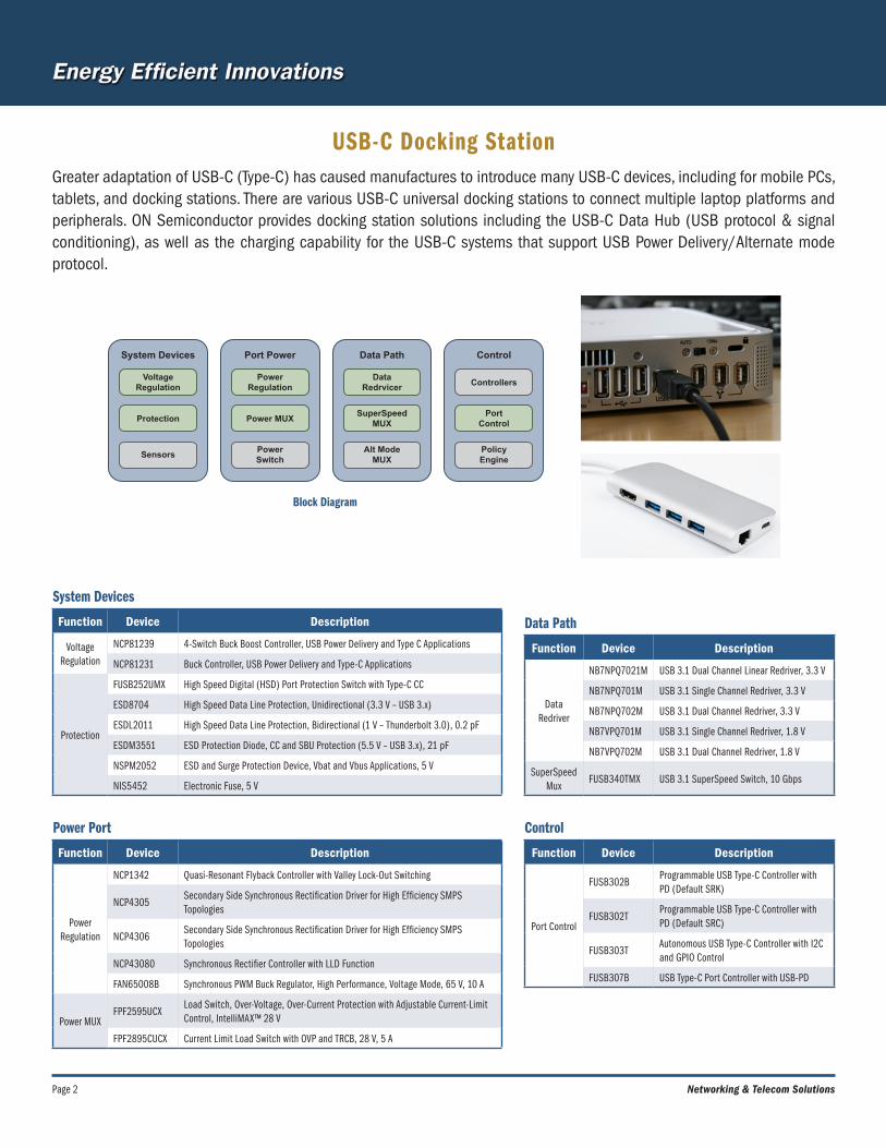
Page 2 Networking & Telecom Solutions
USB-C Docking Station
System Devices
Function Device Description
Voltage Regulation
NCP81239 4-Switch Buck Boost Controller, USB Power Delivery and Type C Applications
NCP81231 Buck Controller, USB Power Delivery and Type-C Applications
Protection
FUSB252UMX High Speed Digital (HSD) Port Protection Switch with Type-C CC
ESD8704 High Speed Data Line Protection, Unidirectional (3.3 V – USB 3.x)
ESDL2011 High Speed Data Line Protection, Bidirectional (1 V – Thunderbolt 3.0), 0.2 pF
ESDM3551 ESD Protection Diode, CC and SBU Protection (5.5 V – USB 3.x), 21 pF
NSPM2052 ESD and Surge Protection Device, Vbat and Vbus Applications, 5 V
NIS5452 Electronic Fuse, 5 V
Power Port
Function Device Description
Power Regulation
NCP1342 Quasi-Resonant Flyback Controller with Valley Lock-Out Switching
NCP4305Secondary Side Synchronous Rectification Driver for High Efficiency SMPS Topologies
NCP4306Secondary Side Synchronous Rectification Driver for High Efficiency SMPS Topologies
NCP43080 Synchronous Rectifier Controller with LLD Function
FAN65008B Synchronous PWM Buck Regulator, High Performance, Voltage Mode, 65 V, 10 A
Power MUXFPF2595UCX
Load Switch, Over-Voltage, Over-Current Protection with Adjustable Current-Limit Control, IntelliMAX™ 28 V
FPF2895CUCX Current Limit Load Switch with OVP and TRCB, 28 V, 5 A
Data Path
Function Device Description
Data Redriver
NB7NPQ7021M USB 3.1 Dual Channel Linear Redriver, 3.3 V
NB7NPQ701M USB 3.1 Single Channel Redriver, 3.3 V
NB7NPQ702M USB 3.1 Dual Channel Redriver, 3.3 V
NB7VPQ701M USB 3.1 Single Channel Redriver, 1.8 V
NB7VPQ702M USB 3.1 Dual Channel Redriver, 1.8 V
SuperSpeed Mux
FUSB340TMX USB 3.1 SuperSpeed Switch, 10 Gbps
Control
Function Device Description
Port Control
FUSB302BProgrammable USB Type-C Controller with PD (Default SRK)
FUSB302TProgrammable USB Type-C Controller with PD (Default SRC)
FUSB303TAutonomous USB Type-C Controller with I2C and GPIO Control
FUSB307B USB Type-C Port Controller with USB-PD
Greater adaptation of USB-C (Type-C) has caused manufactures to introduce many USB-C devices, including for mobile PCs, tablets, and docking stations. There are various USB-C universal docking stations to connect multiple laptop platforms and peripherals. ON Semiconductor provides docking station solutions including the USB-C Data Hub (USB protocol & signal conditioning), as well as the charging capability for the USB-C systems that support USB Power Delivery/Alternate mode protocol.
Block Diagram
System Devices
VoltageRegulation
Protection
Sensors
Port Power
PowerRegulation
Power MUX
PowerSwitch
Data Path
DataRedrvicer
SuperSpeedMUX
Alt ModeMUX
Control
Controllers
PortControl
PolicyEngine

Page 3ON Semiconductor
Crystal
ReferenceClock
Backplane
LoopFilter
Discrete PLL Blocks
Data
Processor
Processor
ASICLatches
Fanout
Divider/Counter
Skew Delay
Receivers
Equalization
MUX
ZDB
Gates
Pre-Emphasis
Crosspoint
PLL ClockGenerator
Gates
Latches
Flip-Flop
ZDB
ASIC
ASIC
Processor
I/O
I/O
I/O
Translator
Flip-Flop
Latches
Gates
PLL ClockGenerator
PLL ClockModule
PLL ClockSynthesizer
VCODivider/
Prescaler
PhaseDetector
MUX
Crosspoint
Pre-Emphasis
Equalization
Fanout
Translator
CMOS/TTLHCSLLVDSPECLCML
PLL ClockModule
TranslatorCMOS/TTL
HCSLLVDS
PECL/CMLPE/EQ
Drivers
Skew Delay
Clock Solutions Data Distribution
ON Semiconductor provides a complete portfolio of timing and data management solutions for all aspects of the clock tree. System designers can optimize their clock circuits with industry leading clock distribution devices, demonstrating the industry’s lowest jitter and skew. A broad product portfolio, with multiple output and interface options, allows system designers to build clock circuits that satisfy their specific application requirements. ON Semiconductor utilizes CMOS, Bipolar, and SiGe technology to leverage the best performance for any given application.
Expanding on more than 30 years of experience as the world’s leader in high performance ECL-based clock distribution, ON Semiconductor has extended its expertise into ultra low jitter PLL clock synthesis and generation. The new PureEdge™ PLL devices utilize a fully differential architecture that enables performance that satisfies the timing requirements for the most demanding applications.
Performance Capabili t ies• Differential design for reduced noise• ECL, PECL, CML, LVDS, M-LVDS, HSTL, HCSL, LVTTL/LVCMOS outputs for
flexible interfacing• Maximum clock rates >10 GHz• Maximum data rates >12 Gbps• Typical additive phase RMS jitter, as low as 30 fs for buffers• Typical phase RMS jitter of 200 fs for clock generators• Integrated termination resistors for simplified circuit design• Edge rates as low as 28 ps• Low phase noise floor ≤ –174 dBc/Hz• Low output-output skew
Timing and Data Distribution Subsystem
Page 4 Networking & Telecom Solutions
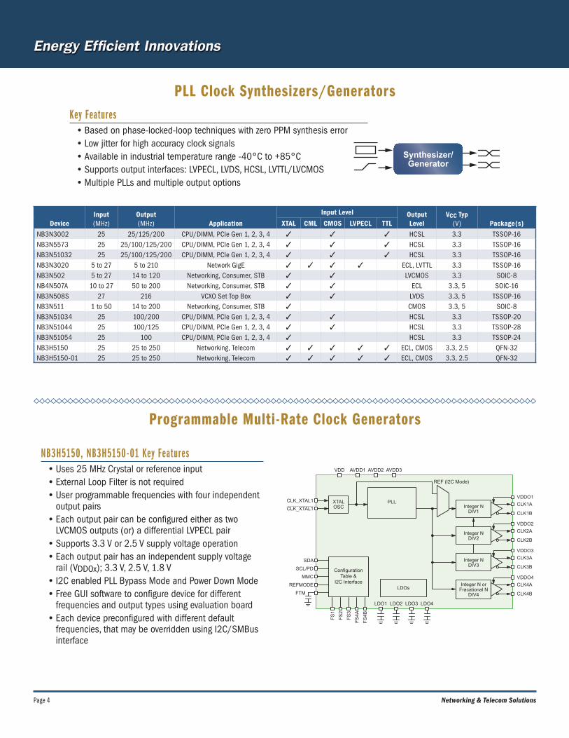
Programmable Multi-Rate Clock Generators
PLL Clock Synthesizers/GeneratorsKey Features
• Based on phase-locked-loop techniques with zero PPM synthesis error• Low jitter for high accuracy clock signals• Available in industrial temperature range -40°C to +85°C• Supports output interfaces: LVPECL, LVDS, HCSL, LVTTL/LVCMOS• Multiple PLLs and multiple output options
NB3H5150, NB3H5150-01 Key Features • Uses 25 MHz Crystal or reference input • External Loop Filter is not required • User programmable frequencies with four independent
output pairs• Each output pair can be configured either as two
LVCMOS outputs (or) a differential LVPECL pair • Supports 3.3 V or 2.5 V supply voltage operation • Each output pair has an independent supply voltage
rail (VDDOx); 3.3 V, 2.5 V, 1.8 V• I2C enabled PLL Bypass Mode and Power Down Mode • Free GUI software to configure device for different
frequencies and output types using evaluation board • Each device preconfigured with different default
frequencies, that may be overridden using I2C/SMBus interface
Synthesizer/Generator
DeviceInput (MHz)
Output (MHz)
Input Level Output Level
VCC Typ (V)Application XTAL CML CMOS LVPECL TTL Package(s)
NB3N3002 25 25/125/200 CPU/DIMM, PCIe Gen 1, 2, 3, 4 3 3 3 HCSL 3.3 TSSOP-16 NB3N5573 25 25/100/125/200 CPU/DIMM, PCIe Gen 1, 2, 3, 4 3 3 3 HCSL 3.3 TSSOP-16 NB3N51032 25 25/100/125/200 CPU/DIMM, PCIe Gen 1, 2, 3, 4 3 3 3 HCSL 3.3 TSSOP-16 NB3N3020 5 to 27 5 to 210 Network GigE 3 3 3 3 ECL, LVTTL 3.3 TSSOP-16 NB3N502 5 to 27 14 to 120 Networking, Consumer, STB 3 3 LVCMOS 3.3 SOIC-8NB4N507A 10 to 27 50 to 200 Networking, Consumer, STB 3 3 ECL 3.3, 5 SOIC-16NB3N508S 27 216 VCXO Set Top Box 3 3 LVDS 3.3, 5 TSSOP-16 NB3N511 1 to 50 14 to 200 Networking, Consumer, STB 3 CMOS 3.3, 5 SOIC-8NB3N51034 25 100/200 CPU/DIMM, PCIe Gen 1, 2, 3, 4 3 3 HCSL 3.3 TSSOP-20NB3N51044 25 100/125 CPU/DIMM, PCIe Gen 1, 2, 3, 4 3 3 HCSL 3.3 TSSOP-28NB3N51054 25 100 CPU/DIMM, PCIe Gen 1, 2, 3, 4 3 HCSL 3.3 TSSOP-24NB3H5150 25 25 to 250 Networking, Telecom 3 3 3 3 3 ECL, CMOS 3.3, 2.5 QFN-32NB3H5150-01 25 25 to 250 Networking, Telecom 3 3 3 3 3 ECL, CMOS 3.3, 2.5 QFN-32
VDDO1
CLK1A
CLK1B
Integer NDIV1
VDDO2
CLK2A
CLK2B
Integer NDIV2
VDDO3
CLK3A
CLK3B
Integer NDIV3
LDOs
XTALOSC
PLL
REF (I2C Mode)
ConfigurationTable &
I2C InterfaceVDDO4
CLK4A
CLK4B
LDO4
Integer N orFracational N
DIV4
LDO3LDO2LDO1
VDD AVDD1 AVDD2 AVDD3
FS
4B
FS
4A
FS
3
FS
2
FS
1
FTM
REFMODE
MMC
SCL/PD
SDA
CLK_XTAL1
CLK_XTAL1
Page 5ON Semiconductor
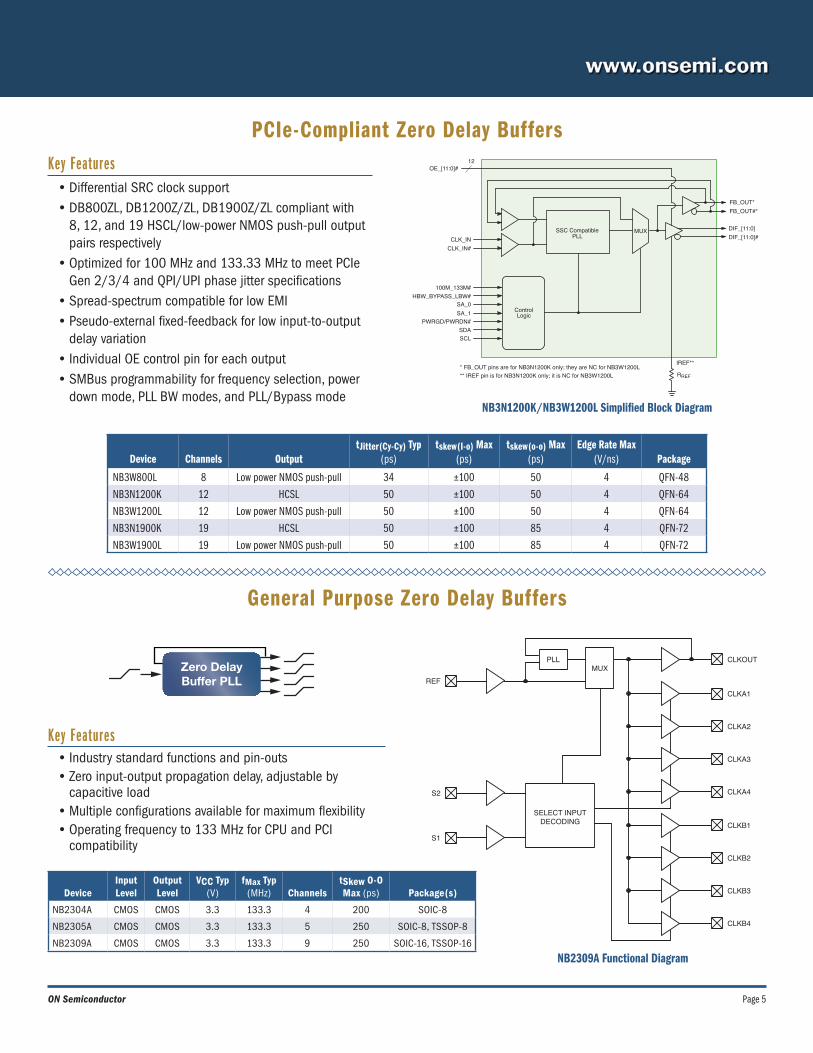
Key Features• Differential SRC clock support• DB800ZL, DB1200Z/ZL, DB1900Z/ZL compliant with
8, 12, and 19 HSCL/low-power NMOS push-pull output pairs respectively
• Optimized for 100 MHz and 133.33 MHz to meet PCIe Gen 2/3/4 and QPI/UPI phase jitter specifications
• Spread-spectrum compatible for low EMI• Pseudo-external fixed-feedback for low input-to-output
delay variation• Individual OE control pin for each output• SMBus programmability for frequency selection, power
down mode, PLL BW modes, and PLL/Bypass mode
General Purpose Zero Delay Buffers
PCIe-Compliant Zero Delay Buffers
CLKOUT
CLKA1
CLKA2
CLKA3
CLKA4
PLLMUX
CLKB1
CLKB2
CLKB3
CLKB4
SELECT INPUTDECODING
REF
S2
S1
Key Features• Industry standard functions and pin-outs• Zero input-output propagation delay, adjustable by
capacitive load• Multiple configurations available for maximum flexibility• Operating frequency to 133 MHz for CPU and PCI
compatibility
NB2309A Functional Diagram
Zero DelayBuffer PLL
DeviceInput Level
Output Level
VCC Typ (V)
fMax Typ (MHz) Channels
tSkew O-O Max (ps) Package(s)
NB2304A CMOS CMOS 3.3 133.3 4 200 SOIC-8
NB2305A CMOS CMOS 3.3 133.3 5 250 SOIC-8, TSSOP-8
NB2309A CMOS CMOS 3.3 133.3 9 250 SOIC-16, TSSOP-16
IREF**
FB_OUT*
DIF_[11:0]
ControlLogic
CLK_INSSC Compatible
PLL
12
SA_0SA_1
SDASCL
MUX
* FB_OUT pins are for NB3N1200K only; they are NC for NB3W1200L** IREF pin is for NB3N1200K only; it is NC for NB3W1200L
100M_133M#
PWRGD/PWRDN#
HBW_BYPASS_LBW#
OE_[11:0]#
CLK_IN#
DIF_[11:0]#
RREF
FB_OUT#*
NB3N1200K/NB3W1200L Simplified Block Diagram
Device Channels OutputtJitter(Cy-Cy) Typ
(ps)tskew(I-o) Max
(ps)tskew(o-o) Max
(ps)Edge Rate Max
(V/ns) Package
NB3W800L 8 Low power NMOS push-pull 34 ±100 50 4 QFN-48
NB3N1200K 12 HCSL 50 ±100 50 4 QFN-64
NB3W1200L 12 Low power NMOS push-pull 50 ±100 50 4 QFN-64
NB3N1900K 19 HCSL 50 ±100 85 4 QFN-72
NB3W1900L 19 Low power NMOS push-pull 50 ±100 85 4 QFN-72
Page 6 Networking & Telecom Solutions
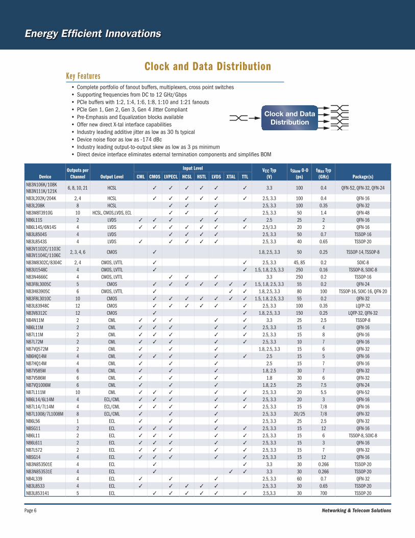
Clock and Data Distribution
Clock and DataDistribution
Key Features• Complete portfolio of fanout buffers, multiplexers, cross point switches• Supporting frequencies from DC to 12 GHz/Gbps• PCIe buffers with 1:2, 1:4, 1:6, 1:8, 1:10 and 1:21 fanouts• PCIe Gen 1, Gen 2, Gen 3, Gen 4 Jitter Compliant• Pre-Emphasis and Equalization blocks available • Offer new direct X-tal interface capabilities • Industry leading additive jitter as low as 30 fs typical• Device noise floor as low as -174 dBc• Industry leading output-to-output skew as low as 3 ps minimum• Direct device interface eliminates external termination components and simplifies BOM
DeviceOutputs per
Channel Output Level
Input Level VCC Typ (V)
tSkew O-O (ps)
fMax Typ (GHz) Package(s)CML CMOS LVPECL HCSL HSTL LVDS XTAL TTL
NB3N106K/108KNB3N111K/121K
6, 8, 10, 21 HCSL 3 3 3 3 3 3 3.3 100 0.4 QFN-52, QFN-32, QFN-24
NB3L202K/204K 2, 4 HCSL 3 3 3 3 3 3 2.5, 3.3 100 0.4 QFN-16NB3L208K 8 HCSL 3 3 3 2.5, 3.3 100 0.35 QFN-32NB3M8T3910G 10 HCSL, CMOS,LVDS, ECL 3 3 3 2.5, 3.3 50 1.4 QFN-48NB6L11S 2 LVDS 3 3 3 3 3 3 2.5 25 2 QFN-16NB6L14S/6N14S 4 LVDS 3 3 3 3 3 3 3 2.5/3.3 20 2 QFN-16NB3L8504S 4 LVDS 3 3 3 3 2.5, 3.3 50 0.7 TSSOP-16NB3L8543S 4 LVDS 3 3 3 3 3 2.5, 3.3 40 0.65 TSSOP-20NB3V1102C/1103CNB3V1104C/1106C
2, 3, 4, 6 CMOS 3 1.8, 2.5, 3.3 50 0.25 TSSOP-14, TSSOP-8
NB3M8302C/8304C 2, 4 CMOS, LVTTL 3 3 2.5, 3.3 45, 85 0.2 SOIC-8NB3U1548C 4 CMOS, LVTTL 3 3 1.5, 1.8, 2.5, 3.3 250 0.16 TSSOP-8, SOIC-8NB3N4666C 4 CMOS, LVTTL 3 3 3 3.3 250 0.2 TSSOP-16NB3F8L3005C 5 CMOS 3 3 3 3 3 3 3 1.5, 1.8, 2.5, 3.3 55 0.2 QFN-24NB3H83905C 6 CMOS, LVTTL 3 3 3 1.8, 2.5, 3.3 80 100 TSSOP-16, SOIC-16, QFN-20NB3F8L3010C 10 CMOS 3 3 3 3 3 3 3 1.5, 1.8, 2.5, 3.3 55 0.2 QFN-32NB3L83948C 12 CMOS 3 3 3 3 3 3 2.5, 3.3 100 0.35 LQFP-32NB3V8312C 12 CMOS 3 3 1.8, 2.5, 3.3 150 0.25 LQFP-32, QFN-32NB4N11M 2 CML 3 3 3 3 3 3.3 25 2.5 TSSOP-8 NB6L11M 2 CML 3 3 3 3 3 2.5, 3.3 15 4 QFN-16NB7L11M 2 CML 3 3 3 3 3 2.5, 3.3 15 8 QFN-16NB7L72M 2 CML 3 3 3 3 3 2.5, 3.3 10 7 QFN-16NB7VQ572M 2 CML 3 3 3 1.8, 2.5, 3.3 15 6 QFN-32NB6HQ14M 4 CML 3 3 3 3 3 2.5 15 5 QFN-16NB7HQ14M 4 CML 3 3 3 2.5 15 7 QFN-16NB7V585M 6 CML 3 3 3 1.8, 2.5 30 7 QFN-32NB7V586M 6 CML 3 3 3 1.8 30 6 QFN-32NB7VQ1006M 6 CML 3 3 3 1.8, 2.5 25 7.5 QFN-24NB7L111M 10 CML 3 3 3 3 3 2.5, 3.3 20 5.5 QFN-52NB6L14/6L14M 4 ECL/CML 3 3 3 3 3 2.5, 3.3 20 3 QFN-16NB7L14/7L14M 4 ECL/CML 3 3 3 3 3 2.5, 3.3 15 7/8 QFN-16NB7L1008/7L1008M 8 ECL/CML 3 3 3 2.5, 3.3 20/25 7/8 QFN-32NB6L56 1 ECL 3 3 3 2.5, 3.3 25 2.5 QFN-32NBSG11 2 ECL 3 3 3 3 3 2.5, 3.3 15 12 QFN-16NB6L11 2 ECL 3 3 3 3 3 2.5, 3.3 15 6 TSSOP-8, SOIC-8NB6L611 2 ECL 3 3 3 3 3 2.5, 3.3 15 3 QFN-16NB7L572 2 ECL 3 3 3 3 3 2.5, 3.3 15 7 QFN-32NBSG14 4 ECL 3 3 3 3 3 2.5, 3.3 15 12 QFN-16NB3N853501E 4 ECL 3 3 3.3 30 0.266 TSSOP-20NB3N853531E 4 ECL 3 3 3 3.3 30 0.266 TSSOP-20NB4L339 4 ECL 3 3 3 2.5, 3.3 60 0.7 QFN-32NB3L8533 4 ECL 3 3 3 3 3 2.5, 3.3 30 0.65 TSSOP-20NB3L853141 5 ECL 3 3 3 3 3 3 2.5,3.3 30 700 TSSOP-20

Page 7ON Semiconductor
Dividers and Counters
Key Features• Low jitter and skew for highly accurate phase matching• Multiple outputs and ratios combined for integrated circuit designs• Supports interface and voltage translation
NB4L339 Functional Diagram
DeviceInput Level Output
LevelVCC Typ
(V)fMax Typ
(GHz) Div Ratios Package(s)CML CMOS LVPECL LVDSNB4L339 3 3 3 3 ECL 2.5, 3.3 0.7 1 or 2; 2; 4; 8 QFN-32NB7V32M 3 3 3 3 CML 1.8, 2.5 10 2 QFN-16NB7N017M 3 3 3 3 CML 3.3 3.5 2 to 256 QFN-52NB7L32M 3 3 3 3 CML 2.5, 3.3 14 2 QFN-16NB6N239S 3 3 3 3 LVDS 3.3 3 1/2/4/8; 2/4/8/16 QFN-16NB6L239 3 3 3 3 ECL 2.5, 3.3 3 1/2/4/8; 2/4/8/16 QFN-16
Counters/Dividers
DIVSEL
CLKSEL
CLKAVTA
CLKA
CLKBVTB
CLKB
EN
MR
5050
5050
EXAMPLE: fin = 622.08 MHz
A÷1 / ÷2
R
B÷2R
C÷4R
D÷8R
EN
QA0QA0QA1QA1
A foutA = 622.08 MHzor 311.04 MHz
QB0QB0QB1QB1
B foutB = 311.04 MHz
QC0QC0QC1QC1
C foutC = 155.52 MHz
QD0QD0QD1QD1
D foutD = 77.76 MHz

Page 8 Networking & Telecom Solutions
Cascadable I/O Expanders
Key Features• I2C and SMBus interfaces• 1 MHz SCL clock frequency• 30 mA SDA sink capability
Vext
Hot-PlugController
Hot-PlugController
ADM1033Thermal Sensor
andFan Controller
Slot 2 Slot 3
GPIO
PCA96xxEPCA95xxE
I/O Expander
I/O
I/O
I/O
I/O
SDAμC
SDASCL
PWRFLTAUXEN
SCL I/O
12 V
MOSFETs
3.3 V
PWRFLTAUXEN
I/OI/O
I/O
PRSNT2I/OPRSNT2I/O
I/O I/O I/O
I/O 12 V
3.3 V
12 V
3.3 V
I/O
ButtonLED
TemperatureControl
KeypadControl
LEDs
BackplaneSystems
INT
Device I/O CascadableVCC Min
(V)VCC Max
(V)Interrupt Output
I/O Pullups
Package
PCA9535E 16 64 Programmable Slave Addresses 1.65 5.5 4 QFN-24, SOIC-24, TSSOP-24
PCA9655E 16 64 Programmable Slave Addresses 1.65 5.5 4 QFN-24, SOIC-24, TSSOP-24
PCA9654E 8 8 Slave ID Addresses 1.65 5.5 4 4 SOIC-16, WQFN-16, TSSOP-16

Page 9ON Semiconductor
Standard Logic and MiniGate™
MiniGate Family
Numberof Gates Device Prefix
VCC
tPD (nS)
IOUT (mA) Input Logic Level Packages
Min(V)
Max (V)
HC 1 MC74HC1G/NC7S 2 6 6.5 @ VCC = 5 V ±5.2 @ VCC = 6 V CMOS
TSOP, SC-88, SC-74, SOT-553, SOT-953, US8, UDFN, UQFN,
MicroPak
HCT 1 NC7ST 4.5 5.5 6.5 @ VCC = 5 V ±2 @ VCC = 6 V TTL
VHC1 MC74VHC1G/NLU1G/NL17SH
1.65 5.5 3.8 @ VCC = 4.5 V ±8 @ VCC = 4.5 V CMOS2 NLU2G3 NLU3G
VHCT1 MC74VHCT1G/NLU1GT/NL17SHT
4.5 5.5 3.6 @ VCC = 4.5 V ±8 @ VCC = 4.5 V TTL2 NLU2GT3 NLU3GT
LCX 1 NL17SZ/NC7SZ/NLX1G
1.65 5.5 2.4 @ VCC = 3 V ±24 @ VCC = 3 V CMOS2 NC27WZ/NC7WZ/NLX2G3 NL37WZ/NC7NZ/NLX3G
VCX 1 NL17SV/NC7SV 0.9 3.6 1.0 @ VCC = 3 V ±24 @ VCC = 3 V LVTTLSG 1 NL17SGxx 0.9 3.6 2.2 @ VCC = 3 V ±8 @ VCC = 3 V LVTTL
SP1 NC7SP
0.9 3.6 3.0 @ VCC = 3 V ±2.6 @ VCC = 3 V LVTTL2 NC7WP3 NC7NP
AUP1 74AUP1G 0.8 3.6 2.9 @ VCC = 3 V ±4 @ VCC = 3 V Schmitt1 74AUP1T 2.3 3.6 3.3 @ VCC = 3 V ±4 @ VCC = 3 V Schmitt
Standard Logic Family Device Prefix
VCC
tPD (nS)
IOUT (mA) Input Logic Level Packages
Min(V)
Max (V)
Metal Gate MC14 3 18 50 @ VCC = 15 V ±4.2 @ VCC = 15 V CMOS
SOIC, TSSOP, QFN
AC MC74AC/74AC 2 6 6 @ VCC = 5 V ±24 @ VCC = 4.5 V CMOS
ACT MC74ACT/74ACT 4.5 5.5 5.5 @ VCC = 5 V ±24 @ VCC = 4.5 V TTL
HC MC74HC/MM74HC 2 6 13 @ VCC = 6 V±5.2 @ VCC = 6 V (Std)
CMOS ±7.8 @ VCC = 6 V (Bus Driver)
HCT MC74HCT/MM74HCT 4.5 5.5 15 @ VCC = 5 V±4.0 @ VCC = 4.5 V (Std)
TTL ±6.0 @ VCC = 4.5 V (Bus Driver)
LCX MC74LCX/74LCX 2.3 3.6 5.5 @ VCC = 3 V ±24 @ VCC = 3 V LVTTL
LVX MC74LVX/74LVX 2 3.6 6.6 @ VCC = 3 V ±4 @ VCC = 3 V LVTTL
VCX MC74VCX/74VCX 1.65 3.6 3.5 @ VCC = 3 V ±24 @ VCC = 3 V LVTTL
VHC MC74VHC/74VHC 2 5.5 5.2 @ VCC = 4.5 V ±8 @ VCC = 4.5 V CMOS
VHCT MC74VHCT/74VHCT 4.5 5.5 3.6 @ VCC = 4.5 V ±8 @ VCC = 4.5 V TTL
LVT 74LVT 2.7 3.6 3.6 @ VCC = 3.0 V -32/64 @ VCC = 3.0 V TTL
Available log ic functions• Logic Gates, Buffers, Flip-Flops• Arithmetic Functions• Bus Transceivers• Latches and Registers• Multiplexers and Analog Switches• Logic Level Translators

Multiphase Controllers with Smart Power Stagesfor Powering CPUs, FPGAs, Core Processors, and DDR Memory
Page 10 Networking & Telecom Solutions
Key Features• Solution supports up to 6 phases; NCP81162 phase doublers allows up to 12 phases• Remote sense for output accuracy• Dual edge modulation for good load transient• Supports DCR or IMON current sensing from power stage
Multiphase ControllersDevice Phases Features Package
NCP81233 Up to 6 I2C for configuration and telemetry QFN-52NCP81232 Up to 4 Dual output or combinable QFN-40NCP81234 Up to 2 Dual output or combinable QFN-28
Power Stages
DeviceIOUT Range
(A)Current Sensing Package
NCP302150 45 (average) DCR PQFN-31NCP302155 55 (average) DCR PQFN-31NCP303150* 80 (peak) IMON PQFN-39FDMF3170 70 (peak) IMON PQFN-39FDMF3180 70 (peak) IMON PQFN-39
* Pending 4Q18
NCP81233 Supports Up to 6 Phase Solution, I2C Interface for Configuration and Telemetry
NCP81232 Supports Up to 4 Phases with 2 Control Loops (Can Be Paralleled for Single Output)
PWM1
Smart PowerStage
PWM2
Smart PowerStage
PWM3SCL
0.9 V/200 A
12 V Input
SDA
INT Smart PowerStage
PWM4
Smart PowerStage
PWM5
Smart PowerStage
PWM6
NCP81233
Smart PowerStage
PWM1
PWM2
PWM3
0.8 V/50 A
12 V Input
Smart PowerStage
PWM4
NCP81232
Smart PowerStage 1 V/50 A
Smart PowerStage
Smart PowerStage
Page 11ON Semiconductor
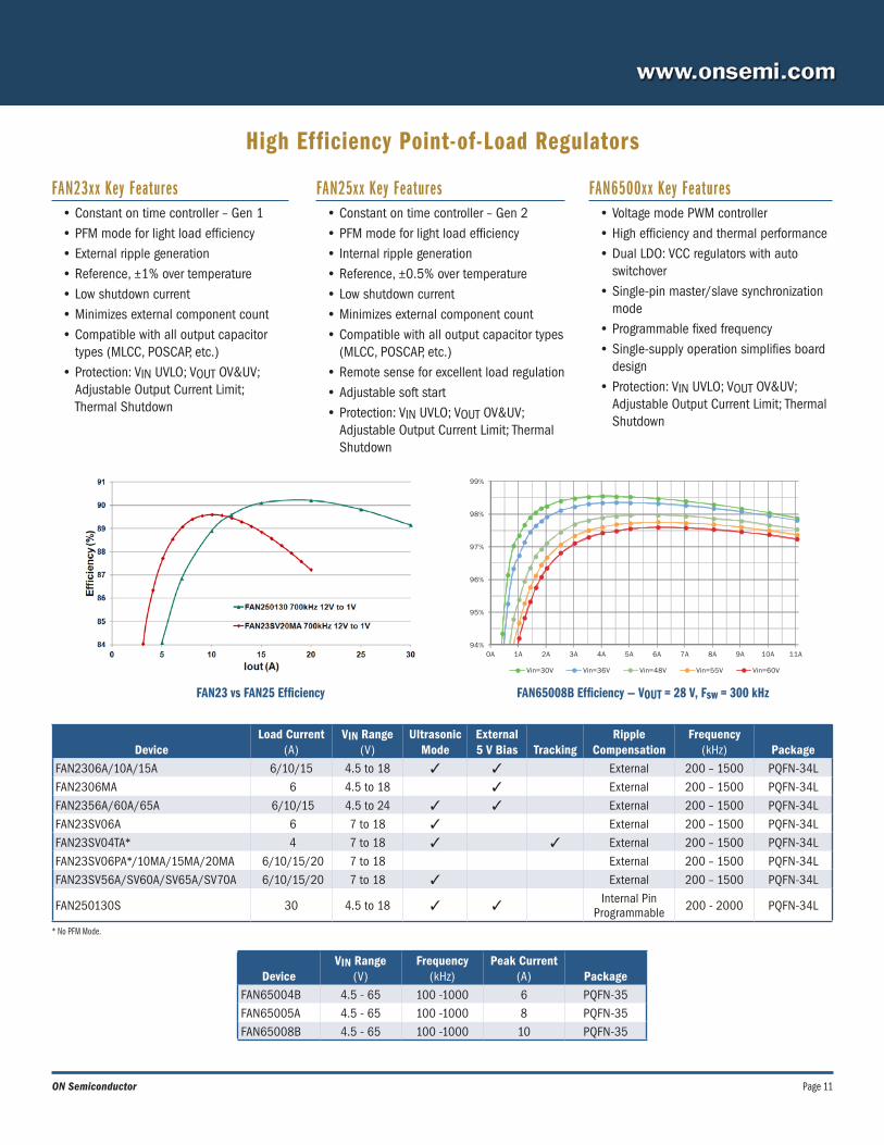
FAN23x x Key Features• Constant on time controller – Gen 1• PFM mode for light load efficiency• External ripple generation• Reference, ±1% over temperature• Low shutdown current• Minimizes external component count• Compatible with all output capacitor
types (MLCC, POSCAP, etc.)• Protection: VIN UVLO; VOUT OV&UV;
Adjustable Output Current Limit; Thermal Shutdown
FAN25x x Key Features• Constant on time controller – Gen 2• PFM mode for light load efficiency• Internal ripple generation• Reference, ±0.5% over temperature• Low shutdown current• Minimizes external component count• Compatible with all output capacitor types
(MLCC, POSCAP, etc.)• Remote sense for excellent load regulation• Adjustable soft start• Protection: VIN UVLO; VOUT OV&UV;
Adjustable Output Current Limit; Thermal Shutdown
FAN6500x x Key Features• Voltage mode PWM controller• High efficiency and thermal performance• Dual LDO: VCC regulators with auto
switchover• Single-pin master/slave synchronization
mode• Programmable fixed frequency• Single-supply operation simplifies board
design• Protection: VIN UVLO; VOUT OV&UV;
Adjustable Output Current Limit; Thermal Shutdown
High Efficiency Point-of-Load Regulators
DeviceLoad Current
(A)VIN Range
(V)Ultrasonic
ModeExternal 5 V Bias Tracking
Ripple Compensation
Frequency (kHz) Package
FAN2306A/10A/15A 6/10/15 4.5 to 18 3 3 External 200 – 1500 PQFN-34L FAN2306MA 6 4.5 to 18 3 External 200 – 1500 PQFN-34L FAN2356A/60A/65A 6/10/15 4.5 to 24 3 3 External 200 – 1500 PQFN-34L FAN23SV06A 6 7 to 18 3 External 200 – 1500 PQFN-34L FAN23SV04TA* 4 7 to 18 3 3 External 200 – 1500 PQFN-34L FAN23SV06PA*/10MA/15MA/20MA 6/10/15/20 7 to 18 External 200 – 1500 PQFN-34L FAN23SV56A/SV60A/SV65A/SV70A 6/10/15/20 7 to 18 3 External 200 – 1500 PQFN-34L
FAN250130S 30 4.5 to 18 3 3Internal Pin
Programmable 200 - 2000 PQFN-34L
DeviceVIN Range
(V)Frequency
(kHz)Peak Current
(A) PackageFAN65004B 4.5 - 65 100 -1000 6 PQFN-35FAN65005A 4.5 - 65 100 -1000 8 PQFN-35FAN65008B 4.5 - 65 100 -1000 10 PQFN-35
* No PFM Mode.
FAN23 vs FAN25 Efficiency
94%
95%
96%
97%
98%
99%
0A 1A 2A 3A 4A 5A 6A 7A 8A 9A 10A 11A
Vin=30V Vin=36V Vin=48V Vin=55V Vin=60V
FAN65008B Efficiency — VOUT = 28 V, Fsw = 300 kHz
Page 12 Networking & Telecom Solutions
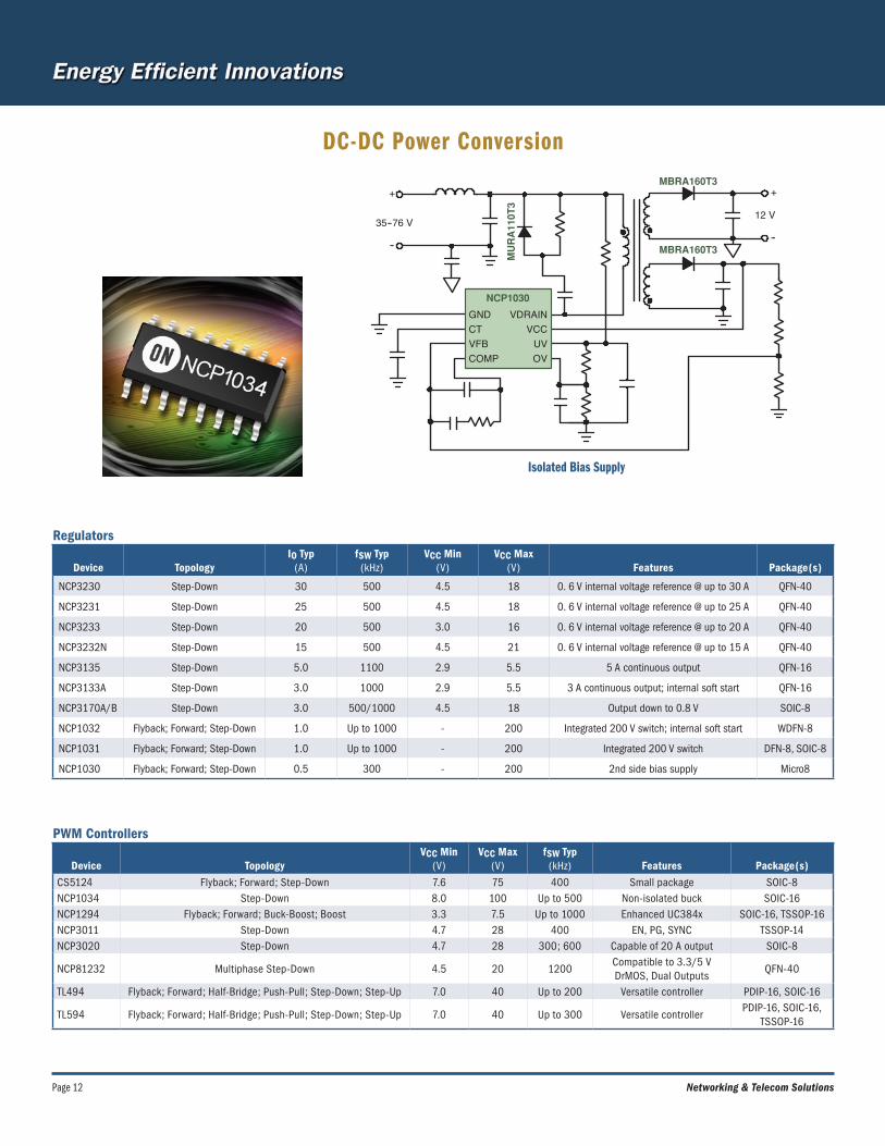
DC-DC Power Conversion
Isolated Bias Supply
+
35--76 V
--
+
--
MBRA160T3
MBRA160T3
12 V
MU
RA
110T
3
GND
COMP
VCCVDRAIN
UVOV
CTVFB
NCP1030
PWM Controllers
Device TopologyVCC Min
(V)VCC Max
(V)fSW Typ (kHz) Features Package(s)
CS5124 Flyback; Forward; Step-Down 7.6 75 400 Small package SOIC-8NCP1034 Step-Down 8.0 100 Up to 500 Non-isolated buck SOIC-16NCP1294 Flyback; Forward; Buck-Boost; Boost 3.3 7.5 Up to 1000 Enhanced UC384x SOIC-16, TSSOP-16NCP3011 Step-Down 4.7 28 400 EN, PG, SYNC TSSOP-14NCP3020 Step-Down 4.7 28 300; 600 Capable of 20 A output SOIC-8
NCP81232 Multiphase Step-Down 4.5 20 1200Compatible to 3.3/5 V DrMOS, Dual Outputs
QFN-40
TL494 Flyback; Forward; Half-Bridge; Push-Pull; Step-Down; Step-Up 7.0 40 Up to 200 Versatile controller PDIP-16, SOIC-16
TL594 Flyback; Forward; Half-Bridge; Push-Pull; Step-Down; Step-Up 7.0 40 Up to 300 Versatile controllerPDIP-16, SOIC-16,
TSSOP-16
Regulators
Device TopologyIO Typ
(A)fSW Typ (kHz)
VCC Min (V)
VCC Max (V) Features Package(s)
NCP3230 Step-Down 30 500 4.5 18 0. 6 V internal voltage reference @ up to 30 A QFN-40
NCP3231 Step-Down 25 500 4.5 18 0. 6 V internal voltage reference @ up to 25 A QFN-40
NCP3233 Step-Down 20 500 3.0 16 0. 6 V internal voltage reference @ up to 20 A QFN-40
NCP3232N Step-Down 15 500 4.5 21 0. 6 V internal voltage reference @ up to 15 A QFN-40
NCP3135 Step-Down 5.0 1100 2.9 5.5 5 A continuous output QFN-16
NCP3133A Step-Down 3.0 1000 2.9 5.5 3 A continuous output; internal soft start QFN-16
NCP3170A/B Step-Down 3.0 500/1000 4.5 18 Output down to 0.8 V SOIC-8
NCP1032 Flyback; Forward; Step-Down 1.0 Up to 1000 - 200 Integrated 200 V switch; internal soft start WDFN-8
NCP1031 Flyback; Forward; Step-Down 1.0 Up to 1000 - 200 Integrated 200 V switch DFN-8, SOIC-8
NCP1030 Flyback; Forward; Step-Down 0.5 300 - 200 2nd side bias supply Micro8
Page 13ON Semiconductor
Linear Voltage Regulators
Device IO Typ Function Features Package
TPS2399 — Hot Swap -36 to -80 V Supply Voltage MSOP-8
TPS2398 — Hot Swap -36 to -80 V Supply Voltage MSOP-8
NCP785A 10 mA High Voltage LDO Up to 450 V VIN; High PSRR SC-89
NCP715 50 mA Ultra-low Quiescent Current LDO Ultra-low quiescent current; Wide input voltage range SC-70-5, DFN-6
NCP716 80 mA Ultra-low Quiescent Current LDO Ultra-low quiescent current; Wide input voltage range WDFN-6
NCP781 100 mA High Voltage LDO Up to 150 V VIN, High PSRR DFN-6
NCP702 200 mA Ultra-low Noise LDO High PSRR; Ultra-low noise SOT-23-5, WDFN-6
NCP160 250 mA Ultra-high PSRR 92 db PSRR; Low Noise WLCSP-4, XDFN-4
NCP163 250 mA Ultra-low Noise 92 db PSRR; 6.5 µVrms Noise WLCSP-4, XDFN-4
NCP703 300 mA Ultra-low Noise LDO Ultra-low noise; High PSRR SOT-23-5, WDFN-6
NCP718 300 mA Ultra-low Quiescent Current LDO Ultra-low quiescent current, Wide input voltage range WDFN-6, TSOT-23-5
NCP161 450 mA Ultra-high PSRR 92 db PSRR; Low Noise WLCSP-4, XDFN-4
NCP133 500 mA Ultra-Low Dropout Voltage Regulator with Bias RailTypical dropout: 140 mV @ 500 mA; High PSRR;
Very fast transient responseXDFN-6
NCP705 500 mA Ultra-low Noise LDO Ultra-low noise; High PSRR WDFN-6
NCP708 1 A Precision LDO 1% Accuracy, Soft start UDFN-6
NCP186 1 A Precision LDO 1% Accuracy, Fast transient response, Ultra low VDO XDFN-8
NCP59800 1 A Low Noise, RF LDO Typical dropout: 200 mV @ 1 A; High PSRR; Ultra-low noise DFN-8
NCP59748 1.5 A Ultra-Low Dropout Voltage Regulator with Bias RailTypical dropout: 60 mV @ 500 mA; High PSRR;
Very fast transient responseDFN-10, QFN-20
NCP51200 3 A DDR3 Termination Regulator Fast load transient response; Soft start; Remote sensing DFN-10
NCP51401 3 A DDR4 Termination Regulator Fast load transient response; Soft start; Remote sensing DFN-10
NCP59744 3 A Ultra-Low Dropout Voltage Regulator with Bias Rail Typical dropout: 115 mV @ 3 A; High PSRR; Very fast transient response QFN-20
NCP59749 3 A Ultra-Low Dropout Voltage Regulator with Bias Rail Typical dropout: 120 mV @ 3 A; High PSRR; Very fast transient response DFN-10, QFN-20
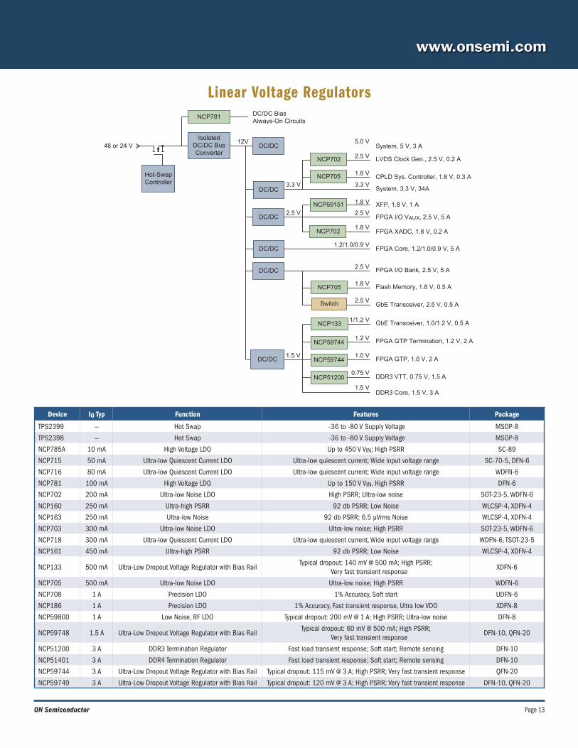
System, 5 V, 3 A
LVDS Clock Gen., 2.5 V, 0.2 A
CPLD Sys. Controller, 1.8 V, 0.3 A
System, 3.3 V, 34A
XFP, 1.8 V, 1 A
FPGA I/O VAUX, 2.5 V, 5 A
FPGA XADC, 1.8 V, 0.2 A
FPGA Core, 1.2/1.0/0.9 V, 5 A
FPGA I/O Bank, 2.5 V, 5 A
Flash Memory, 1.8 V, 0.5 A
GbE Transceiver, 2.5 V, 0.5 A
GbE Transceiver, 1.0/1.2 V, 0.5 A
FPGA GTP Termination, 1.2 V, 2 A
FPGA GTP, 1.0 V, 2 A
DDR3 VTT, 0.75 V, 1.5 A
DDR3 Core, 1.5 V, 3 A
DC/DC
12V
NCP705
DC/DC
48 or 24 V
NCP59744DC/DC
NCP133
DC/DC
DC/DC
NCP59151
NCP702
Hot-SwapController
NCP705
NCP702
NCP781 DC/DC BiasAlways-On Circuits
DC/DC
NCP59744
NCP51200
Switch
Isolated DC/DC BusConverter
5.0 V
2.5 V
1.8 V
3.3 V3.3 V
1.8 V
2.5 V2.5 V
1.8 V
1.2/1.0/0.9 V
2.5 V
1.8 V
2.5 V
1/1.2 V
1.2 V
1.0 V1.5 V
0.75 V
1.5 V

Page 14 Networking & Telecom Solutions
Device Voltage Range Current Range Key Features Functions Packages
SuperJunction MOSFET
600 – 800 V 1.6 – 75 A
• Outstanding ease of use and low EMI • Excellent FOM (RDS(ON) max. X Qg typ.)• Well balanced switching behavior• Robust body diode• Soft recovery and small Qrr for FRFET
High voltage switch for indus-trial power supply
D2PAK, DPAK, IPAK, TO-220,
TO-220F, TO-247, Power88
Wide Selection of High Voltage Power MOSFETs
Key Features• SuperFET® III Easy Drive
n Outstanding ease of use and low EMI n Excellent Figure-of-Merit (RDS(ON) Max X Qg Typ)n Well balanced switching behaviorn V(BR)DSS of 650 V at Tj = 25°C, 700 V at Tj = 150°Cn Robust body diode
• SuperFET® III FRFET®n No need additional circuit in LLC resonant convertern Improving system reliabilityn Best in class body diode performance (trr, Qrr,
robustness)n Soft recovery and low peak VDS during body diode
turn-off transientn V(BR)DSS of 650 V at Tj = 25°C, 700 V at Tj = 150°C
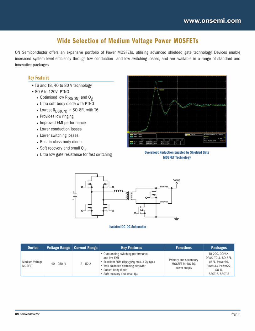
ON Semiconductor offers an expansive portfolio of Power MOSFETs, utilizing advanced SuperJunction technology. Devices enable increased system level efficiency through low switching and low conduction losses, and are available in a range of standard and innovative packages.
AC-DC Rectifier Typical Block Diagram
48 V DCOutput
110-240 VAC Input
LLCPFC
FastRecovery
EasyDrive
Gate oscillation during turn-off transient
-50 -40 -30 -20 -10 0 10 20 30 40 50-16
-12
-8
-4
0
4
8
12
16
Vgs
[V]
Time [ns]
SF3 EasyDrive Comtetitor
SuperFET III Easy DriveCompetitor
Body Diode Performance
SuperFET III Fast Recovery Best Competitor
Page 15ON Semiconductor
Device Voltage Range Current Range Key Features Functions Packages
Medium Voltage MOSFET
40 – 250 V 2 – 52 A
• Outstanding switching performance and low EMI • Excellent FOM (RDS(ON) max. X Qg typ.)• Well balanced switching behavior• Robust body diode• Soft recovery and small Qrr
Primary and secondary MOSFET for DC-DC
power supply
TO-220, D2PAK, DPAK, TOLL, SO-8FL,
µ8FL, Power56, Power33, Power22,
SO-8, SSOT-6, SSOT-3
Wide Selection of Medium Voltage Power MOSFETs
Key Features• T6 and T8, 40 to 80 V technology• 80 V to 120V PTNG
n Optimised low RDS(ON) and Qgn Ultra soft body diode with PTNGn Lowest RDS(ON) in SO-8FL with T6n Provides low ringingn Improved EMI performancen Lower conduction lossesn Lower switching lossesn Best in class body dioden Soft recovery and small Qrrn Ultra low gate resistance for fast switching
ON Semiconductor offers an expansive portfolio of Power MOSFETs, utilizing advanced shielded gate technology. Devices enable increased system level efficiency through low conduction and low switching losses, and are available in a range of standard and innovative packages.
Isolated DC-DC Schematic
Vout
Overshoot Reduction Enabled by Shielded Gate MOSFET Technology
Page 16 Networking & Telecom Solutions
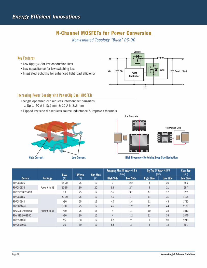
High Frequency Switching Loop Size Reduction
2 x Discrete
1 x Power Clip
Non-Isolated Topology “Buck” DC-DC
Key Features• Low RDS(ON) for low conduction loss• Low capacitance for low switching loss• Integrated Schottky for enhanced light load efficiency
Increasing Power Densit y with PowerClip Dual MOSFETs• Single optimized clip reduces interconnect parasitics
n Up to 40 A in 5x6 mm & 25 A in 3x3 mm
• Flipped low side die reduces source inductance & improves thermals
Sync Cout VoutVin Cin
Control
PWMController
N-Channel MOSFETs for Power Conversion
Device PackageImax(A)
BVDSS(V)
VGS Max(V)
RDS(ON) Max @ VGS= 4.5 V (mΩ)
Qg Typ @ VGS= 4.5 V (nC)
Coss Typ(pF)
High Side Low Side High Side Low Side Low SideFDPC8012S
Power Clip 33
15-20 25 12 7 2.2 8 25 885
FDPC8013S 10-15 30 20 9.6 2.7 6 21 997
FDPC3D5N025X9D 10 25 12 3.7 3.7 17 17 612
FDPC8016S
Power Clip 56
20-30 25 12 4.7 1.7 11 31 1195
FDPC8014S >30 25 12 4.7 1.4 11 43 1720
FDPC8014AS >30 25 12 4.7 1.2 11 44 2170
FDMS001N025DSD >30 25 16 4 1.1 10 35 1810
FDMS1D2N03DSD >30 30 16 4 1.2 11 39 1845
FDPC5018SG 25 30 12 6.5 2 8 28 1210
FDPC5030SG 20 30 12 6.5 3 8 18 801
High Current Low Current
Page 17ON Semiconductor
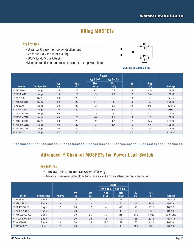
ORing MOSFETs
Advanced P-Channel MOSFETs for Power Load Switch
ConfigurationVDS (V)
VGS (V)
RDS(ON)
Qg (nC)
Qgd (nC)
VGS @ 10 V VGS @ 4.5 V
DeviceMax
(mΩ)Max
(mΩ) PackageNTMFS4H01N Single 25 20 0.7 0.9 39 8.5 SO8-FL
NTMFS4H02N Single 25 20 1.3 1.9 26 5.8 SO8-FL
FDMS8050 Single 30 20 0.65 0.9 93 18 Power56
NTMFS4C020N Single 30 20 0.7 1 63 13 SO8-FL
FDMC8010 Single 30 20 1.3 1.8 32 9.5 Power33
NTTFS4C02N Single 30 20 2.3 3.1 20 4 U8FL
NTMFS5C404NL Single 40 20 0.67 1 81 23.8 SO8-FL
NTMFS5H400NL Single 40 20 0.8 1.1 54 13 SO8-FL
NTMFS5C604NL Single 60 20 1.2 1.7 52 12.7 SO8-FL
NTMFS5H600NL Single 60 20 1.3 1.7 40 6.5 SO8-FL
NTMTS6H800N Single 80 20 2.1 — 85 16 SO8-FL
FDMS86180 Single 100 20 3.2 — 60 12 Power56
Configuration PolarityVDS (V)
VGS (V)
RDS(ON)
Qg (nC)
Ciss (pF)
VGS @ 10 V VGS @ 4.5 V
DeviceMax
(mΩ)Max
(mΩ) PackageFDMC610P Single P 12 8 — 3.9 71 890 Power33
NTLUS3C18PZ Single P 12 10 — 24 16 1570 UDFN-6
FDMC4D9P20X8 Single P 20 12 — 4.9 78 7535 PQFN-8
FDMA008P20LZ Single P 20 8 — 13 28 3131 PQFN-6
NTMFS002P03P8Z Single P 30 25 1.7 2.8 242 14712 SO-8FL HE
NTTFS008P03P8P Single P 30 25 4.5 7.2 85 5246 Power33
FDMA6676PZ Single P 30 25 13.5 27 20 1440 PQFN-6
NTLUD3A50PZ Dual P 20 8 — 48 10.4 920 UDFN-6
Key Features• Ultra low RDS(ON) for low conduction loss• 25 V and 30 V for IM bus ORing•100 V for 48 V bus ORing•Much more efficient and reliable solution than power diodes
Key Features• Ultra low RDS(ON) to improve system efficiency• Advanced package technology for space saving and excellent thermal conduction
MOSFETs as ORing Diodes
=
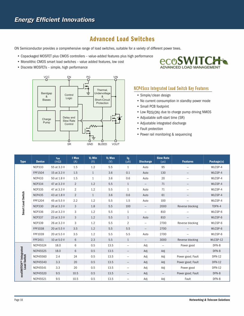
Advanced Load Switches
• Copackaged MOSFET plus CMOS controllers – value-added features plus high performance• Monolithic CMOS smart load switches – value added features, low cost• Discrete MOSFETs – simple, high performance
ON Semiconductor provides a comprehensive range of load switches, suitable for a variety of different power trees.
NCP45x x x Integrated Load Switch Key Features• Simple/clean design• No current consumption in standby power mode• Small PCB footprint• Low RDS(ON) due to charge pump driving NMOS• Adjustable soft-start time (SR)• Adjustable integrated discharge• Fault protection• Power rail monitoring & sequencing
Thermal,Undervoltage
&Short-CircuitProtection
ControlLogic
Bandgap&
Biases
Delay andSlew Rate
Control
ChargePump
VIN
VOUTBLEEDGNDSR
PGENVCC
Type Deviceron
(mΩ) I Max
(A) VI Min
(V) VI Max
(V) IQ
(mA) DischargeSlew Rate
(ms) Features Package(s)
Smar
t Loa
d Sw
itch
NCP333 55 at 3.3 V 1.5 1.2 5.5 1 Auto 95 — WLCSP-4
FPF1504 15 at 3.3 V 1.5 1 3.6 0.1 Auto 130 — WLCSP-4
NCP433 50 at 1.8 V 1.5 1 3.6 0.6 Auto 20 — WLCSP-4
NCP334 47 at 3.3 V 2 1.2 5.5 1 — 71 — WLCSP-4
NCP335 47 at 3.3 V 2 1.2 5.5 1 Auto 71 — WLCSP-4
NCP435 43 at 1.8 V 2 1 3.6 0.6 Auto 61 — WLCSP-4
FPF1204 45 at 5.5 V 2.2 1.2 5.5 1.5 Auto 100 — WLCSP-4
NCP330 26 at 3.3 V 3 1.8 5.5 100 — 2000 Reverse blocking TDFN-4
NCP336 23 at 3.3 V 3 1.2 5.5 1 — 810 — WLCSP-6
NCP337 23 at 3.3 V 3 1.2 5.5 1 Auto 810 — WLCSP-6
NCP339 26 at 3.3 V 3 1.2 5.5 2 — 2700 Reverse blocking WLCSP-6
FPF1038 20 at 5.5 V 3.5 1.2 5.5 5.5 — 2700 — WLCSP-6
FPF1039 20 at 5.5 V 3.5 1.2 5.5 5.5 Auto 2700 — WLCSP-6
FPF2411 10 at 5.0 V 6 2.3 5.5 1 — 3000 Reverse blocking WLCSP-12
ecoS
WIT
CH™
Inte
grat
ed
Load
Sw
itch
NCP45524 18.0 6 0.5 13.5 — Adj — Power good DFN-8
NCP45525 18.0 6 0.5 13.5 — Adj Adj — DFN-8
NCP45560 2.4 24 0.5 13.5 — Adj Adj Power good; Fault DFN-12
NCP45540 3.3 20 0.5 13.5 — Adj Adj Power good; Fault DFN-12
NCP45541 3.3 20 0.5 13.5 — Adj Adj Power good DFN-12
NCP45520 9.5 10.5 0.5 13.5 — Adj — Power good; Fault DFN-8
NCP45521 9.5 10.5 0.5 13.5 — Adj Adj Fault DFN-8
Page 18 Networking & Telecom Solutions
Page 19ON Semiconductor
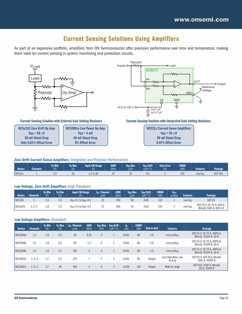
Current Sensing Solutions Using Amplifiers
Low Voltage, Zero Drift Amplifiers (High Precision)
Device ChannelsVS Min
(V)VS Max
(V)Input CM Range
(V)IQ /Channel
(mA)GBW(kHz)
VOS Max(mV)
VOS Drift (mV/°C)
CMRR(dB)
ep-p(mVpp) Features Package
NCS325 1 1.8 5.5 VSS–0.1 to VDD+0.1 21 350 50 0.02 110 1 Low VOS SOT-23
NCSx333 1, 2, 4 1.8 5.5 VSS–0.1 to VDD+0.1 21 350 10 0.03 120 1 Low VOSSOT-23-5, SC-70-5, DFN-8, Micro8, SOIC-8, SOIC-14
Low Voltage Amplifiers (Standard)
Device ChannelsVS Min
(V)VS Max
(V)IQ /Channel
(mA)GBW(MHz)
VOS Max(mV)
VOS Drift (mV/°C)
IB (nA)
CMRR(dB) Rail-to-Rail Features Package
NCS2009x 1,2 1.8 5.5 20 0.35 4 1 0.001 80 I/O Low IQ &VOSSOT-23-5. SC-70-5, UDFN-6,
Micro8, TSSOP-8, SO-8
NCS2008x 1,2 1.8 5.5 50 1.2 4 1 0.001 80 I/O Low IQ &VOSSOT-23-5. SC-70-5, UDFN-6,
Micro8, TSSOP-8, SO-8
NCS2006x 1,2 1.8 5.5 140 3 4 1 0.001 80 I/O Low IQ &VOSSOT-23-5. SC-70-5, UDFN-6,
Micro8, TSSOP-8, SO-8
NCS2003x 1, 2, 4 1.7 5.5 275 7 5 2 0.001 80 Output Fast Slew Rate, Low VS & IB
SOT-23-5, SOT-553, Micro8, SOIC-8, TSSOP-8
NCS2007x 1, 2, 4 2.7 36 400 3 4 2 0.005 110 Output Wide VS range SOT-553, TSOP-5, Micro8, SO-8, TSSOP-8
Zero Drift Current Sense Amplifiers (Integrated and Precision Performance)
Device ChannelsVS Min
(V)VS Max
(V)Input CM Range
(V)GBW(kHz)
VOS Max(mV)
VOS Drift (mV/°C)
Gain Error(%)
CMRR(dB) Features Package
NCS21x 1 2.2 26 2.2 to 26 14 35 0.5 1 140 Low VOS SOT-363
As part of an expansive portfolio, amplifiers from ON Semiconductor offer precision performance over time and temperature, making them ideal for current sensing in system monitoring and protection circuits.
Op Amp
Load
VLoad
RSENSE
NCSx333 Zero Drift Op AmpVOS = 10 mV
50 mV Shunt DropOnly 0.02% Offset Error
NCS200xx Low Power Op AmpVOS = 4 mV
50 mV Shunt Drop8% Offset Error
NCS213
IN–
IN+
OUTOutput
ReferenceVoltage
0.01 μFto 0.1 μF
+2.2 to +26 V
Supply Load
GNDVS
RSHUNT
REF
NCS21x Current Sense AmplifiersVOS = 35 mV
50 mV Shunt Drop0.07% Offset Error
Current Sensing Solution with External Gain Setting Resistors Current Sensing Solution with Integrated Gain Setting Resistors
Page 20 Networking & Telecom Solutions
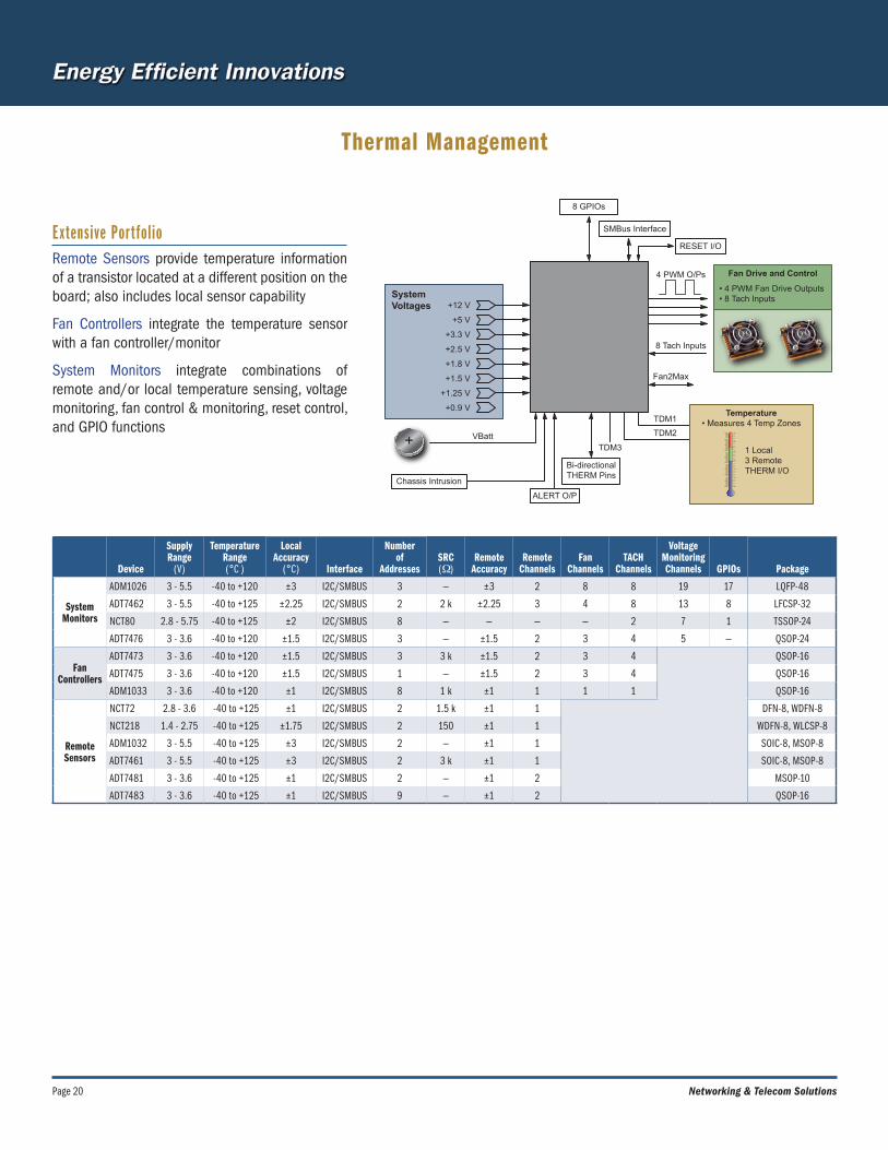
Thermal Management
Ex tensive Por t folio Remote Sensors provide temperature information of a transistor located at a different position on the board; also includes local sensor capability
Fan Controllers integrate the temperature sensor with a fan controller/monitor
System Monitors integrate combinations of remote and/or local temperature sensing, voltage monitoring, fan control & monitoring, reset control, and GPIO functions
SystemVoltages +12 V
+5 V
+3.3 V
+2.5 V
+1.8 V
+1.5 V
+1.25 V
+0.9 V
VBatt
Chassis Intrusion
ALERT O/P
Bi-directionalTHERM Pins
TDM3
TDM1
TDM2
8 GPIOs
SMBus Interface
RESET I/O
Fan Drive and Control
• 4 PWM Fan Drive Outputs• 8 Tach Inputs
4 PWM O/Ps
8 Tach Inputs
Fan2Max
Temperature• Measures 4 Temp Zones
1 Local3 RemoteTHERM I/O
Device
Supply Range
(V)
Temperature Range(°C )
LocalAccuracy
(°C) Interface
Numberof
AddressesSRC(Ω)
RemoteAccuracy
RemoteChannels
FanChannels
TACHChannels
Voltage Monitoring Channels GPIOs Package
System Monitors
ADM1026 3 - 5.5 -40 to +120 ±3 I2C/SMBUS 3 — ±3 2 8 8 19 17 LQFP-48
ADT7462 3 - 5.5 -40 to +125 ±2.25 I2C/SMBUS 2 2 k ±2.25 3 4 8 13 8 LFCSP-32
NCT80 2.8 - 5.75 -40 to +125 ±2 I2C/SMBUS 8 — — — — 2 7 1 TSSOP-24
ADT7476 3 - 3.6 -40 to +120 ±1.5 I2C/SMBUS 3 — ±1.5 2 3 4 5 — QSOP-24
Fan Controllers
ADT7473 3 - 3.6 -40 to +120 ±1.5 I2C/SMBUS 3 3 k ±1.5 2 3 4 QSOP-16
ADT7475 3 - 3.6 -40 to +120 ±1.5 I2C/SMBUS 1 — ±1.5 2 3 4 QSOP-16
ADM1033 3 - 3.6 -40 to +120 ±1 I2C/SMBUS 8 1 k ±1 1 1 1 QSOP-16
Remote Sensors
NCT72 2.8 - 3.6 -40 to +125 ±1 I2C/SMBUS 2 1.5 k ±1 1 DFN-8, WDFN-8
NCT218 1.4 - 2.75 -40 to +125 ±1.75 I2C/SMBUS 2 150 ±1 1 WDFN-8, WLCSP-8
ADM1032 3 - 5.5 -40 to +125 ±3 I2C/SMBUS 2 — ±1 1 SOIC-8, MSOP-8
ADT7461 3 - 5.5 -40 to +125 ±3 I2C/SMBUS 2 3 k ±1 1 SOIC-8, MSOP-8
ADT7481 3 - 3.6 -40 to +125 ±1 I2C/SMBUS 2 — ±1 2 MSOP-10
ADT7483 3 - 3.6 -40 to +125 ±1 I2C/SMBUS 9 — ±1 2 QSOP-16
Page 21ON Semiconductor
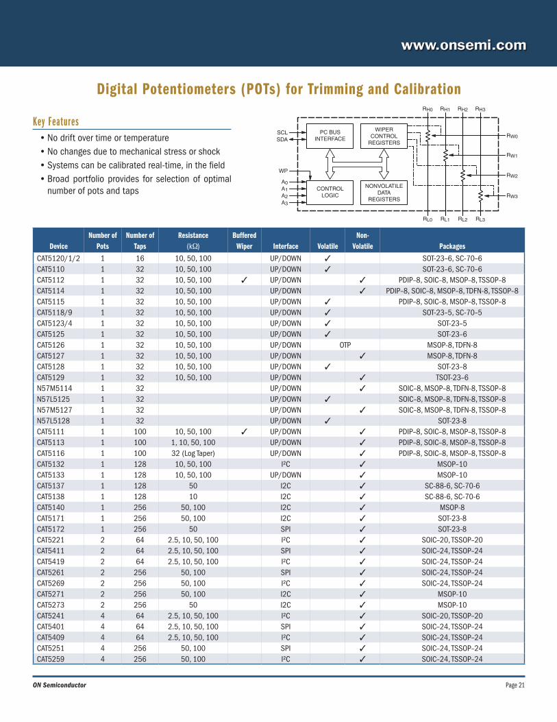
Digital Potentiometers (POTs) for Trimming and Calibration
Key Features• No drift over time or temperature• No changes due to mechanical stress or shock• Systems can be calibrated real-time, in the field• Broad portfolio provides for selection of optimal
number of pots and tapsNONVOLATILE
DATAREGISTERS
WIPERCONTROL
REGISTERS
CONTROLLOGIC
PC BUSINTERFACE
SCL RW0
RH0 RH1 RH2 RH3
RL0 RL1 RL2 RL3
RW1
RW2
RW3
SDA
A0
WP
A1A2A3
DeviceNumber of
PotsNumber of
Taps Resistance
(kΩ)Buffered
Wiper Interface VolatileNon-
Volatile Packages
CAT5120/1/2 1 16 10, 50, 100 UP/DOWN 3 SOT-23–6, SC-70–6CAT5110 1 32 10, 50, 100 UP/DOWN 3 SOT-23–6, SC-70–6CAT5112 1 32 10, 50, 100 3 UP/DOWN 3 PDIP–8, SOIC–8, MSOP–8, TSSOP–8CAT5114 1 32 10, 50, 100 UP/DOWN 3 PDIP–8, SOIC–8, MSOP–8, TDFN-8, TSSOP–8CAT5115 1 32 10, 50, 100 UP/DOWN 3 PDIP–8, SOIC–8, MSOP–8, TSSOP–8CAT5118/9 1 32 10, 50, 100 UP/DOWN 3 SOT-23–5, SC-70–5CAT5123/4 1 32 10, 50, 100 UP/DOWN 3 SOT-23–5CAT5125 1 32 10, 50, 100 UP/DOWN 3 SOT-23–6CAT5126 1 32 10, 50, 100 UP/DOWN OTP MSOP-8, TDFN-8CAT5127 1 32 10, 50, 100 UP/DOWN 3 MSOP-8, TDFN-8CAT5128 1 32 10, 50, 100 UP/DOWN 3 SOT-23–8CAT5129 1 32 10, 50, 100 UP/DOWN 3 TSOT-23–6N57M5114 1 32 UP/DOWN 3 SOIC–8, MSOP–8, TDFN-8, TSSOP–8N57L5125 1 32 UP/DOWN 3 SOIC–8, MSOP–8, TDFN-8, TSSOP–8N57M5127 1 32 UP/DOWN 3 SOIC–8, MSOP–8, TDFN-8, TSSOP–8N57L5128 1 32 UP/DOWN 3 SOT-23-8CAT5111 1 100 10, 50, 100 3 UP/DOWN 3 PDIP–8, SOIC–8, MSOP–8, TSSOP–8CAT5113 1 100 1, 10, 50, 100 UP/DOWN 3 PDIP–8, SOIC–8, MSOP–8, TSSOP–8CAT5116 1 100 32 (Log Taper) UP/DOWN 3 PDIP–8, SOIC–8, MSOP–8, TSSOP–8CAT5132 1 128 10, 50, 100 I²C 3 MSOP–10CAT5133 1 128 10, 50, 100 UP/DOWN 3 MSOP–10CAT5137 1 128 50 I2C 3 SC-88-6, SC-70-6CAT5138 1 128 10 I2C 3 SC-88-6, SC-70-6CAT5140 1 256 50, 100 I2C 3 MSOP-8CAT5171 1 256 50, 100 I2C 3 SOT-23-8CAT5172 1 256 50 SPI 3 SOT-23-8CAT5221 2 64 2.5, 10, 50, 100 I²C 3 SOIC–20, TSSOP–20CAT5411 2 64 2.5, 10, 50, 100 SPI 3 SOIC–24, TSSOP–24CAT5419 2 64 2.5, 10, 50, 100 I²C 3 SOIC–24, TSSOP–24CAT5261 2 256 50, 100 SPI 3 SOIC–24, TSSOP–24CAT5269 2 256 50, 100 I²C 3 SOIC–24, TSSOP–24CAT5271 2 256 50, 100 I2C 3 MSOP-10CAT5273 2 256 50 I2C 3 MSOP-10CAT5241 4 64 2.5, 10, 50, 100 I²C 3 SOIC–20, TSSOP–20CAT5401 4 64 2.5, 10, 50, 100 SPI 3 SOIC–24, TSSOP–24CAT5409 4 64 2.5, 10, 50, 100 I²C 3 SOIC–24, TSSOP–24CAT5251 4 256 50, 100 SPI 3 SOIC–24, TSSOP–24CAT5259 4 256 50, 100 I²C 3 SOIC–24, TSSOP–24
Switching Devices
Page 22 Networking & Telecom Solutions
ON Semiconductor offers a range of switching devices for high speed interface in servers, desktop computing, notebook and netbook computers. Applications include PCI Express, DisplayPort, Gigabit Ethernet and USB 2.0.
Processor
Gigabit LANTransceiver
InternalGraphics
Processor
ExternalGraphics
Processor
North Bridge(ICH)
South Bridge(MCH)
VGA Switch
Do
ckin
g S
tati
on
Co
nn
ecto
r PCIeSwitch
HDMI/DVISwitch
LAN Switch
USB Power/Data Switch
Codec
Stereo Switch
Mic Switch
TMDSDisplayPort
Switch
2nd LCDDisplay
LCDPanel
AudioAmp
Server Implementation
Device Interface Data RateNo
ChannelsQuiescent Current
NCN1188 USB 2.0 / MHL 2.25 Gb/s 2 21 μA
NS5S1153 USB 2.0 480 Mb/s 2 21 μA
NLAS7242 USB 2.0 480 Mb/s 2 1 μA
NLAS4684 Audio 9.5 MHz 2 180 nA
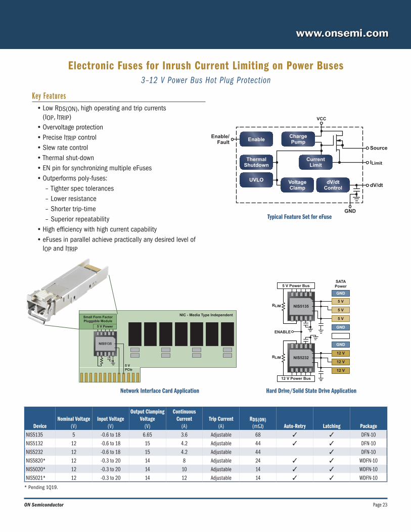
Electronic Fuses for Inrush Current Limiting on Power Buses3–12 V Power Bus Hot Plug Protection
Key Features• Low RDS(ON), high operating and trip currents
(IOP, ITRIP)• Overvoltage protection• Precise ITRIP control• Slew rate control• Thermal shut-down • EN pin for synchronizing multiple eFuses• Outperforms poly-fuses:
– Tighter spec tolerances– Lower resistance– Shorter trip-time– Superior repeatability
• High efficiency with high current capability• eFuses in parallel achieve practically any desired level of
IOP and ITRIP
ChargePumpEnable
Enable/Fault
GND
Source
ILimit
dV/dt
CurrentLimit
VoltageClamp
dV/dtControl
ThermalShutdown
UVLO
VCC
Typical Feature Set for eFuse
Hard Drive/Solid State Drive ApplicationNetwork Interface Card Application
5 V Power BusSATAPower
NIS5135
NIS5232
RLIM
ENABLE
12 V Power Bus
RLIM
12 V
12 V
12 V
GND
GND
5 V
5 V
5 V
GND
Small Form FactorPluggable Module
NIS5135
5 VPCIe
NIC - Media Type Independent
5 V Power
Page 23ON Semiconductor
DeviceNominal Voltage
(V)Input Voltage
(V)
Output Clamping Voltage
(V)
ContinuousCurrent
(A)Trip Current
(A)RDS(ON)
(mΩ) Auto-Retry Latching Package
NIS5135 5 -0.6 to 18 6.65 3.6 Adjustable 68 3 3 DFN-10
NIS5132 12 -0.6 to 18 15 4.2 Adjustable 44 3 3 DFN-10
NIS5232 12 -0.6 to 18 15 4.2 Adjustable 44 3 DFN-10
NIS5820* 12 -0.3 to 20 14 8 Adjustable 24 3 3 WDFN-10
NIS5020* 12 -0.3 to 20 14 10 Adjustable 14 3 3 WDFN-10
NIS5021* 12 -0.3 to 20 14 12 Adjustable 14 3 3 WDFN-10
* Pending 1Q19.

Page 24 Networking & Telecom Solutions
Ethernet : 10/100BASE-T, 1000BASE-TX, and GigabitSurge/ESD Protection for Four Pairs
Line-to-Line Surge
Line Side : LC03-6 (optional)Transformer Side: TVS8818
Protection against metallic (transverse) strikes
Typical ApplicationKey Features• Line-to-line capacitance < 3 pF• Vclamp (25 A surge) < 11 V• IEC 61000-4-2 rating > 30 kV• No latching danger• Surge rating maintained to 125°C
Benef it s• Compatible with Gb Ethernet and beyond• Enhanced protection for downstream electronics• Accommodates operating transients above 3.3 V• Small form-factor allows integration into connectors
The 1000BASE-T or Gigabit Ethernet interface operating at higher bitrates is susceptible to ESD strikes, cable-discharge events and lightning-induced transients. Our products help meet IEC 61000-4-5, GR-1089-CORE and other Standards.
C5VDDC1
C2
TVS8818
LC03
C3
C4
C6VDD
LC03
C7VDD
LC03
C8VDD
LC03
TPOPA
TPONA
TPOPB
TPONB
TPOPC
TPONC
TPOPD
TPOND
A+
A-
B+
B-
C+
C-
D+
D-
1000
BA
SE
-TE
TH
ER
NE
T T
RA
NS
CE
IVE
R
TR
AN
SF
OR
ME
R
RJ4
5
1 8
1 8
1 8
1 8
-10 00
5
10
15
20
25
30
10 20 30Time (μs)
Vo
ltag
e (V
), C
urr
ent
(A)
40 50 60
8/20 μsSurge Current
ON SemiconductorVoltage
CompetitorVoltage
1
2
3
4
5
6
7
8
RJ-
45 C
on
nec
tor
Flow ThroughRouting
TVS8818
Surge Protection Devices
DeviceVDC Max
(V)
Line Transient
Max (V)
Surge IPP, 8/20 ms
(A)
Typical Line-Line
Capacitance(pF)
ESD Contact Rating
(kV) PackageLC03-6 6.7 7.0 100 8.0 ±30 SOIC-8TVS8814 3.0 3.2 35 1.5 ±30 UDFN-8TVS8818 3.0 3.2 35 1.5 ±30 UDFN-10SRDA3.3 3.3 5.0 25 4.0 ±8 SOIC-8SRDA05 5.0 7.0 23 5.0 ±8 SOIC-8NUP4114H 5.0 5.0 12* 0.4 ±13 TSOP-6
* On Pin 5.
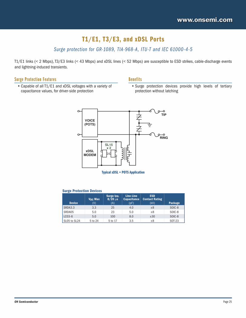
T1/E1, T3/E3, and xDSL PortsSurge protection for GR-1089, TIA-968-A, ITU-T and IEC 61000-4-5
Surge Protection Features• Capable of all T1/E1 and xDSL voltages with a variety of
capacitance values, for driver-side protection
Benef it s• Surge protection devices provide high levels of tertiary
protection without latching
T1/E1 links (< 2 Mbps), T3/E3 links (< 43 Mbps) and xDSL lines (< 52 Mbps) are susceptible to ESD strikes, cable-discharge events and lightning-induced transients.
SL15x 2
TIP
RING
VOICE(POTS)
xDSLMODEM
Typical xDSL + POTS Application
Surge Protection Devices
DeviceVDC Max
(V)
Surge IPP, 8/20 ms
(A)
Line-Line Capacitance
(pF)
ESD Contact Rating
(kV) PackageSRDA3.3 3.3 25 4.0 ±8 SOIC-8SRDA05 5.0 23 5.0 ±8 SOIC-8LC03-6 5.0 100 8.0 ±30 SOIC-8SL05 to SL24 5 to 24 5 to 17 3.5 ±8 SOT-23
Page 25ON Semiconductor
Page 26 Networking & Telecom Solutions
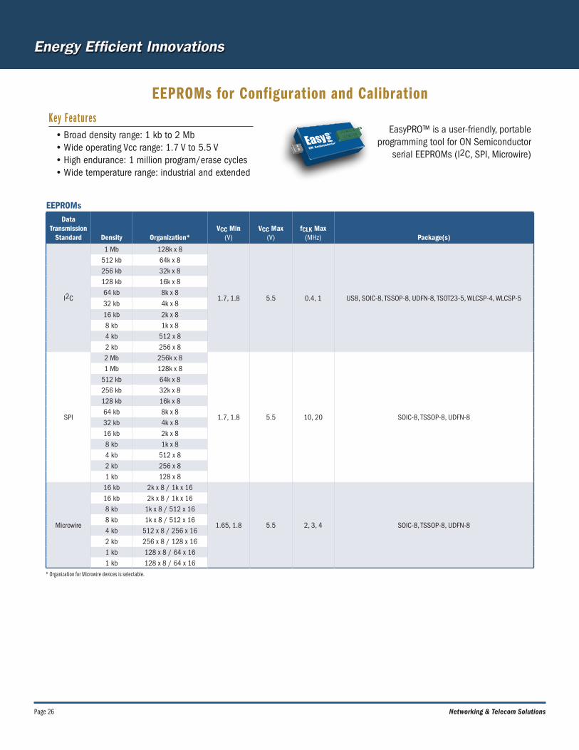
EEPROMs for Configuration and Calibration
EasyPRO™ is a user-friendly, portable programming tool for ON Semiconductor
serial EEPROMs (I2C, SPI, Microwire)
Key Features• Broad density range: 1 kb to 2 Mb• Wide operating Vcc range: 1.7 V to 5.5 V• High endurance: 1 million program/erase cycles• Wide temperature range: industrial and extended
EEPROMsData
Transmission Standard Density Organization*
VCC Min(V)
VCC Max(V)
fCLK Max(MHz) Package(s)
I2C
1 Mb 128k x 8
1.7, 1.8 5.5 0.4, 1 US8, SOIC-8, TSSOP-8, UDFN-8, TSOT23-5, WLCSP-4, WLCSP-5
512 kb 64k x 8256 kb 32k x 8128 kb 16k x 864 kb 8k x 8
32 kb 4k x 8
16 kb 2k x 88 kb 1k x 84 kb 512 x 82 kb 256 x 8
SPI
2 Mb 256k x 8
1.7, 1.8 5.5 10, 20 SOIC-8, TSSOP-8, UDFN-8
1 Mb 128k x 8512 kb 64k x 8256 kb 32k x 8128 kb 16k x 864 kb 8k x 832 kb 4k x 816 kb 2k x 88 kb 1k x 84 kb 512 x 82 kb 256 x 81 kb 128 x 8
Microwire
16 kb 2k x 8 / 1k x 16
1.65, 1.8 5.5 2, 3, 4 SOIC-8, TSSOP-8, UDFN-8
16 kb 2k x 8 / 1k x 168 kb 1k x 8 / 512 x 168 kb 1k x 8 / 512 x 164 kb 512 x 8 / 256 x 162 kb 256 x 8 / 128 x 161 kb 128 x 8 / 64 x 161 kb 128 x 8 / 64 x 16
* Organization for Microwire devices is selectable.
Page 27ON Semiconductor
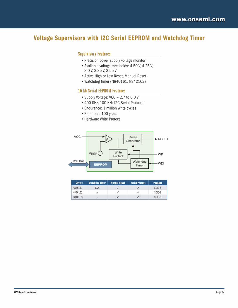
Voltage Supervisors with I2C Serial EEPROM and Watchdog Timer
Supervisor y Features• Precision power supply voltage monitor• Available voltage thresholds: 4.50 V, 4.25 V,
3.0 V, 2.85 V, 2.55 V• Active High or Low Reset, Manual Reset• Watchdog Timer (N84C161, N84C163)
16 kb Serial EEPROM Features• Supply Voltage: VCC = 2.7 to 6.0 V• 400 KHz, 100 KHz I2C Serial Protocol• Endurance: 1 million Write cycles• Retention: 100 years• Hardware Write Protect
Device Watchdog Timer Manual Reset Write Protect Package
N84C161 SDA 3 3 SOIC-8
N84C162 — 3 3 SOIC-8
N84C163 — 3 3 SOIC-8
DelayGenerator
RESETVCC
I2C Bus
WP
WDI
WriteProtect
VREF
WatchdogTimerEEPROM
BRD8077/DBRD8077-7 PRINTED IN USA 11/18 IRONWOOD XXXX 500
SuperFET and FRFET are registered trademarks and EasyPRO, ecoSWITCH, IntelliMAX, MiniGate, and PureEdge are trademarks of ON Semiconductor. All other brand names and product names appearing in this document are trademarks of their respective holders.
ON Semiconductor and the ON Semiconductor logo are trademarks of Semiconductor Components Industries, LLC dba ON Semiconductor or its subsidiaries in the United States and/or other countries. ON Semiconductor owns the rights to a number of patents, trademarks, copyrights, trade secrets, and other intellectual property. A listing of ON Semiconductor’s product/patent coverage may be accessed at www.onsemi.com/site/pdf/Patent-Marking.pdf. ON Semiconductor reserves the right to make changes without further notice to any products herein. ON Semiconductor makes no warranty, representation or guarantee regarding the suitability of its products for any particular purpose, nor does ON Semiconductor assume any liability arising out of the application or use of any product or circuit, and specifically disclaims any and all liability, including without limitation special, consequential or incidental damages. Buyer is responsible for its products and applications using ON Semiconductor products, including compliance with all laws, regulations and safety requirements or standards, regardless of any support or applications information provided by ON Semiconductor. “Typical” parameters which may be provided in ON Semiconductor data sheets and/or specifications can and do vary in different applications and actual performance may vary over time. All operating parameters, including “Typicals” must be validated for each customer application by customer’s technical experts. ON Semiconductor does not convey any license under its patent rights nor the rights of others. ON Semiconductor products are not designed, intended, or authorized for use as a critical component in life support systems or any FDA Class 3 medical devices or medical devices with a same or similar classification in a foreign jurisdiction or any devices intended for implantation in the human body. Should Buyer purchase or use ON Semiconductor products for any such unintended or unauthorized application, Buyer shall indemnify and hold ON Semiconductor and its officers, employees, subsidiaries, affiliates, and distributors harmless against all claims, costs, damages, and expenses, and reasonable attorney fees arising out of, directly or indirectly, any claim of personal injury or death associated with such unintended or unauthorized use, even if such claim alleges that ON Semiconductor was negligent regarding the design or manufacture of the part. ON Semiconductor is an Equal Opportunity/Affirmative Action Employer. This literature is subject to all applicable copyright laws and is not for resale in any manner.
LITERATURE FULFILLMENT: Literature Distribution Center for ON Semiconductor 19521 E. 32nd Pkwy, Aurora, Colorado 80011 USA Phone: 303-675-2175 or 800-344-3860 Toll Free USA/Canada Fax: 303-675-2176 or 800-344-3867 Toll Free USA/Canada Email: [email protected]
N. American Technical Support: 800-282-9855 Toll Free USA/Canada.Europe, Middle East and Africa Technical Support:
Phone: 421 33 790 2910Japan Customer Focus Center Phone: 81-3-5817-1050
ON Semiconductor Website: www.onsemi.com
Order Literature: http://www.onsemi.com/orderlit
For additional information, please contact your local Sales Representative
PUBLICATION ORDERING INFORMATION
Sales and Design Assistance from ON Semiconductor
AMERICAS REP FIRMSAlabama Huntsville e-Components (256) 533-2444Brazil Countrywide Ammon & Rizos (+55) 11-4688-1960California Bay Area Electec (408) 496-0706Canada Eastern Canada Astec (905) 607-1444Connecticut Statewide Paragon Electronic Systems (603) 645-7630Florida Statewide e-Components (888) 468-2444Georgia Atlanta e-Components (888) 468-2444Illinois Statewide Matrix – Design Technology (952) 400-1070Indiana Fishers Bear VAI (317) 570-0707Iowa Statewide Matrix – Design Technology (319) 362-6824Maine Statewide Paragon Electronic Systems (603) 645-7630Maryland Columbia Mechtronics Sales (410) 309-9600Massachusetts Statewide Paragon Electronic Systems (603) 645-7630Mexico Countrywide Ammon & Rizos (+55) 11-4688-1960Michigan St. Joseph Bear VAI (440) 526-1991Minnesota Eden Prairie Matrix – Design Technology (952) 400-1070Missouri Belton Matrix – Design Technology (816) 589-2308Nebraska Statewide Matrix – Design Technology (816) 589-2308New Hampshire Statewide Paragon Electronic Systems (603) 645-7630New Jersey Statewide S.J. Metro (516) 942-3232New York Binghamton TriTech - Full Line Rep (607) 722-3580
Jericho S.J. Metro (516) 942-3232Rochester TriTech - Full Line Rep (585) 385-6500
North Carolina Raleigh e-Components (888) 468-2444North Dakota Statewide Matrix – Design Technology (952) 400-1070Ohio Brecksville Bear VAI Technology (440) 526-1991Puerto Rico Countrywide e-Components (888) 468-2444Rhode Island Statewide Paragon Electronic Systems (603) 645-7630South Dakota Statewide Matrix – Design Technology (952) 400-1070Vermont Statewide Paragon Electronic Systems (603) 645-7630Wisconsin Statewide Matrix – Design Technology (952) 400-1070
ON Semiconductor Distribution PartnersAllied Electronics www.alliedelec.com (800) 433-5700
ALTIMA Company, Macnica, Inc. www.alt.macnica.co.jp/about/english.html (81) 45 476 2155
Arrow Electronics www.arrow.com (800) 777-2776
Avnet www.em.avnet.com (800) 332-8638
Chip One Stop, Inc. www.chip1stop.com/web/JPN/en/maker/on (81) 45 470 8770
CLAVIS Company, Macnica, Inc. www.macnica.co.jp/en (81) 45 470 9821
Daiwa Distribution Ltd. www.daiwahk.com (852) 2341 3351
Digi-Key www.digikey.com (800) 344-4539
EBV Elektronik www.ebv.com/en/locations.html (49) 8121 774-0
Future & FAI Electronics www.futureelectronics.com/contact 1-800-FUTURE1 (388-8731)
Fuji Electronics Co., Ltd. www.fujiele.co.jp/english (81) 3 3814 1411
KTL Corporation www.ktl-corp.co.jp/en (81) 3 5639 1104
Mouser Electronics www.mouser.com (800) 346-6873
Newark/Farnell www.farnell.com/onsemi (800) 4-NEWARK
NEXTY Electronics Corporation www.nexty-ele.com/english (81) 52 558 4161
OS Electronics Co., Ltd. www.oselec.com Japanese: (81) 3 3255 5985Other Languages: (81) 3 3255 6066
Promate Electronic Co. www.promate.com.tw (886) 2 2659 0303
Ryoden Corporation www.ryoden.co.jp/en (81) 3 5396 6310
Ryosan Company, Limited www.ryosan.co.jp/eng (81) 3 3862 2635
RS Components www.rs-components.com (44) 153 644 4414
Segyung Britestone Co. www.britestone.com (82) 2 3218 1511
Serial Microelectronics, HK www.serialsys.com.hk (852) 2790 8220
World Peace Industries Co. www.wpi-group.com (852) 2365 4860
WT Microelectronics Co. www.wtmec.com (852) 2950 0820
Yosun Electronics www.yosun.com.tw (886) 2 2659 8168
ON SEMICONDUCTOR INTERNATIONAL SALES OFFICESGREATER CHINA Beijing 86-10-8577-8200
Hong Kong 852-2689-0088Shenzhen 86-755-8209-1128Shanghai 86-21-5131-7168Taipei, Taiwan 886-2-2377-9911
FRANCE Paris 33 (0)1 39-26-41-00GERMANY Munich 49 (0) 89-93-0808-0INDIA Bangalore 91-98-808-86706ISRAEL Raanana 972 (0) 9-9609-111ITALY Milan 39 02 9239311JAPAN Tokyo 81-3-5427-3066KOREA Seoul 82-31-786-3700MALAYSIA Penang 60-4-6463877SINGAPORE Singapore 65-6484-8603SLOVAKIA Piestany 421 33 790 2450UNITED KINGDOM Maidenhead 44 (0) 1628 244326
www.onsemi.com/supportON Semiconductor Technical Support
For a comprehensive listing of ON Semiconductor Sales Offices, Distributors,
and Rep Firms, please visit:
Americas & EMEA: www.onsemi.com/salesChina: www.onsemi.cn/salesJapan: www.onsemi.jp/sales
May-17
Mouser Electronics
Authorized Distributor
Click to View Pricing, Inventory, Delivery & Lifecycle Information: ON Semiconductor:
NCP6336BFCCT1G