MAX14657/MAX14658/ MAX14659 Dual-Channel USB Host ...
28
MAX14657/MAX14658/ MAX14659 Dual-Channel USB Host Adapter Emulators General Description The MAX14657/MAX14658/MAX14659 are next-genera- tion dual-channel USB 2.0 host-charger adapter emula- tors that combine USB Hi-Speed analog switches with a USB adapter emulator circuit. The MAX14657 features an I 2 C interface to fully configure the charging behavior with different address options. The MAX14658/MAX14659 are controlled by two GPIO inputs (CB1_/CB0_) and support USB data and automatic charger mode. In charging downstream port (CDP) mode, the devices emulate the CDP function while supporting normal USB traffic. The MAX14657/MAX14658 have a CEN_ output for an active-high CLS enable input, and the MAX14659 has a CEN_ output for an active-low CLS enable input to restart the peripheral connected to the USB host. The MAX14658/MAX14659 feature 2A high-current autodetect mode. The MAX14657 can be configured through I 2 C to support various dedicated charger modes such as Apple 1A/2A forced, or Apple or Samsung 1A/2A autodetect modes. The MAX14657/MAX14658/MAX14659 support CDP and standard downstream port (SDP) charging while in the active state (S0), and support the dedicated charging port (DCP) charging while in the standby state (S3/S4/ S5). All of the devices support low-speed remote wake-up by monitoring DM_, and also support remote wakeup in sleep mode (S3). The MAX14657/MAX14658/MAX14659 are available in a 16-pin (3mm x 3mm) TQFN-EP package and are speci- fied over the -40°C to +85°C extended temperature range. Applications ● Laptop/Desktop Computers ● USB Hubs ● Universal Chargers Including iPod®/iPhone®/iPad® iPod®/iPhone®/iPad® are registered trademarks of Apple, Inc Benefits and Features ● Integrated Dual Channels • More Convenient, High-Current USB Charging Ports for Users • Simple and Flexible Power-Management Control • Small TQFN Package Minimizes PCB Area ● Improved Charger Interoperability • USB (CDP) Emulation with Smart CDP and Fool- Proof CDP • Enhanced Automodes • Foolproof CDP • Meets New USB Battery Charging (BC) Revision 1.2 Specification • Backward Compatible with Previous USB BC Revisions • Meets China YD/T1591-2009 Charging Specification • Supports Standby-Mode Charging for USB BC Revision 1.2 Compatible Devices ● Provide Greater Application Flexibility • I 2 C Controls Multiple Modes (MAX14657) • A Slave Address Selection Input Offers Two Possible Slave Addresses for Each Emulator (MAX14657) • CB0_ and CB1_ Pins Control Multiple Automatic and Manual Charger States (MAX14658, MAX14659) ● Enhance Performance with High Level of Integrated Features • Supports Remote Wake-Up • Low-Capacitance USB 2.0 Hi-Speed Switch to Change Charging Modes • Automatic Current-Limit Switch Control • ±15kV ESD Protection on DP_/DM_ Selector Guide 19-6664; Rev 1; 8/13 Ordering Information and Typical Operating Circuit appear at end of data sheet. For related parts and recommended products to use with this part, refer to www.maximintegrated.com/MAX14657.related. PART NUMBER I/O MODE CEN POLARITY REMOTE WAKE-UP IN AM MAX14657 I 2 C Programmable (CEN default) Programmable MAX14658 GPIO CEN Yes MAX14659 GPIO CEN Yes
-
Upload
khangminh22 -
Category
Documents
-
view
0 -
download
0
Transcript of MAX14657/MAX14658/ MAX14659 Dual-Channel USB Host ...
MAX14657/MAX14658/MAX14659
Dual-Channel USB Host Adapter Emulators
General DescriptionThe MAX14657/MAX14658/MAX14659 are next-genera-tion dual-channel USB 2.0 host-charger adapter emula-tors that combine USB Hi-Speed analog switches with a USB adapter emulator circuit.The MAX14657 features an I2C interface to fully configure the charging behavior with different address options. The MAX14658/MAX14659 are controlled by two GPIO inputs (CB1_/CB0_) and support USB data and automatic charger mode. In charging downstream port (CDP) mode, the devices emulate the CDP function while supporting normal USB traffic. The MAX14657/MAX14658 have a CEN_ output for an active-high CLS enable input, and the MAX14659 has a CEN_ output for an active-low CLS enable input to restart the peripheral connected to the USB host.The MAX14658/MAX14659 feature 2A high-current autodetect mode. The MAX14657 can be configured through I2C to support various dedicated charger modes such as Apple 1A/2A forced, or Apple or Samsung 1A/2A autodetect modes.The MAX14657/MAX14658/MAX14659 support CDP and standard downstream port (SDP) charging while in the active state (S0), and support the dedicated charging port (DCP) charging while in the standby state (S3/S4/S5). All of the devices support low-speed remote wake-up by monitoring DM_, and also support remote wakeup in sleep mode (S3).The MAX14657/MAX14658/MAX14659 are available in a 16-pin (3mm x 3mm) TQFN-EP package and are speci-fied over the -40°C to +85°C extended temperature range.
Applications Laptop/DesktopComputers USBHubs UniversalChargersIncludingiPod®/iPhone®/iPad®
iPod®/iPhone®/iPad® are registered trademarks of Apple, Inc
Benefits and Features IntegratedDualChannels
• More Convenient, High-Current USB Charging Ports for Users • Simple and Flexible Power-Management Control • Small TQFN Package Minimizes PCB Area
ImprovedChargerInteroperability • USB (CDP) Emulation with Smart CDP and Fool- Proof CDP • Enhanced Automodes • Foolproof CDP • Meets New USB Battery Charging (BC) Revision 1.2 Specification • Backward Compatible with Previous USB BC Revisions • Meets China YD/T1591-2009 Charging Specification • Supports Standby-Mode Charging for USB BC Revision 1.2 Compatible Devices
ProvideGreaterApplicationFlexibility • I2C Controls Multiple Modes (MAX14657) • A Slave Address Selection Input Offers Two Possible Slave Addresses for Each Emulator (MAX14657) • CB0_ and CB1_ Pins Control Multiple Automatic and Manual Charger States (MAX14658, MAX14659)
EnhancePerformancewithHighLevelofIntegratedFeatures • Supports Remote Wake-Up • Low-Capacitance USB 2.0 Hi-Speed Switch to Change Charging Modes • Automatic Current-Limit Switch Control • ±15kV ESD Protection on DP_/DM_
Selector Guide
19-6664; Rev 1; 8/13
Ordering Information and Typical Operating Circuit appear at end of data sheet.
For related parts and recommended products to use with this part, refer to www.maximintegrated.com/MAX14657.related.
PART NUMBER
I/O MODE
CEN POLARITY
REMOTE WAKE-UP IN
AM
MAX14657 I2C Programmable (CEN default) Programmable
MAX14658 GPIO CEN YesMAX14659 GPIO CEN Yes

MAX14657/MAX14658/MAX14659
Dual-Channel USB Host Adapter Emulators
www.maximintegrated.com Maxim Integrated 2
Electrical Characteristics(VCC = 3.0V to 5.5V, TA = -40°C to +85°C, unless otherwise noted. Typical values are at VCC = +5.0V and TA = +25°C.) (Note 2)
Note 1: Package thermal resistances were obtained using the method described in JEDEC specification JESD51-7, using a four-layer board. For detailed information on package thermal considerations, refer to www.maximintegrated.com/thermal-tutorial.
(All voltages referenced to GND.)VCC, TDP_, TDM_, DP_, DM_, SDA,
SCL, CB0_, CB1_, CEN_, CEN_, SAS, INT .......-0.3V to +6VContinuous Current into Any Terminal ..............................±30mAContinuous Power Dissipation (TA = +70°C)
TQFN (derate 20.8mW/°C above +70°C)...............1666.7mW
Operating Temperature Range ........................... -40°C to +85°CJunction Temperature ......................................................+150°CStorage Temperature Range ............................ -65°C to +150°CLead Temperature (soldering, 10s) .................................+300°CSoldering Temperature (reflow) .......................................+260°C
Stresses beyond those listed under “Absolute Maximum Ratings” may cause permanent damage to the device. These are stress ratings only, and functional operation of the device at these or any other conditions beyond those indicated in the operational sections of the specifications is not implied. Exposure to absolute maximum rating conditions for extended periods may affect device reliability.
Package Thermal Characteristics (Note 1)TQFN Junction-to-AmbientThermalResistance(θJA) ..........48°C/W Junction-to-CaseThermalResistance(θJC) ...............10°C/W
Absolute Maximum Ratings
PARAMETER SYMBOL CONDITIONS MIN TYP MAX UNITSPOWER SUPPLY
VCC Supply Voltage VCC
MAX14658MAX14659
CB0_ = high/CB1_ = low (PM mode)CB0_ = low/CB1_ = high (FM mode)
3.0 5.5
V
MAX14657
MODE_SEL[2:0] = 001 (PM mode)MODE_SEL[2:0 ] = 010 (FM mode)
MAX14658MAX14659
CB0_ = low/CB1_ = low (AM2 mode)CB0_ = high/CB1_ = high (CM mode) (Note 3)
4.75 5.25
MAX14657
MODE_SEL[2:0] = XXX except:MODE_SEL[2:0] = 001 (PM mode)MODE_SEL[2:0] = 010 (FM mode) (Note 3)

MAX14657/MAX14658/MAX14659
Dual-Channel USB Host Adapter Emulators
www.maximintegrated.com Maxim Integrated 3
Electrical Characteristics (continued)(VCC = 3.0V to 5.5V, TA = -40°C to +85°C, unless otherwise noted. Typical values are at VCC = +5.0V and TA = +25°C.) (Note 2)
PARAMETER SYMBOL CONDITIONS MIN TYP MAX UNITS
VCC Supply Current ICC
MAX14658MAX14659
CB1_ = CB0_ = low (AM2 mode) 120
µA
CB1_ = CB0_ = high (CM mode) 150
CB1 _ = low/CB0_ = high (PM mode) 25
MAX14657
MODE_SEL[2:0] = 000 (AM2 mode) 120
MODE_SEL[2:0] = 011 (CM mode) 150
MODE_SEL[2:0] = 001 (PM mode) 25
POR Delay tPOR 50 msANALOG SWITCHES (DP_, DM_, TDP_, TDM_)Analog Signal Range VDP, VDM (Note 4) 0 VCC V
TDP_/TDM_ On-Resistance RON VCC = 3V, VIN = 0V, VCC, IIN = 10mA 3.5 6.5 Ω
TDP_/TDM_ On-Resistance Matching Between Channels ΔRON VCC = 3V, VIN = 0V, VCC, IIN = 10mA 0.1 Ω
TDP_/TDM_ On-Resistance Flatness RFLAT VCC = 3V, VIN = 0V, VCC, IIN = 10mA 0.1 Ω
DP_/DM_ Short On-Resistance RSHORT VDP = 1V, RL=20kΩonDM_ 70 130 Ω
Off-Leakage Current ICOM(OFF)VCC = 3.6V, VDP = VDM = 0.3V, 3.3V;VTDP_ = VTDM_ = 0.3V, 3.3V -1000 +1000 nA
On-Leakage Current ICOM(ON) VCC = 3.6V, VDP_ = VDM_ = 0.3V, 3.3V -1000 90 +1000 nADYNAMIC PERFORMANCE
Turn-On Time tONVTDP_ or VTDM_ = 1.5V, RL=300Ω, CL = 35pF, Figure 1 10 µs
Turn-Off Time tOFFVTDP or VTDM = 1.5V, RL=300Ω, CL = 35pF, Figure 1 10 µs
TDP_/TDM_ Propagation Delay tPHL, tPLHRL = RS=50Ω,DP_andDM_connectedto TDP_ and TDM_, Figure 2 60 ps
DP_/DM_ Output Skew tSKEWRL = RS=50Ω,DP_andDM_connectedto TDP_ and TDM_, Figure 2 40 ps
DP_/DM On-Capacitance (Connected to TDP_, TDM_) CON f = 240MHz, VBIAS = 0V, VIN = 500mVP-P 5 pF
Bandwidth BW RL = RS=50Ω,Figure3 1000 MHz
Off-Isolation VISOVIN = 0dBm, RL = RS=50Ω,f=250MHz,Figure 3 -20 dB
Crosstalk VCTVIN = 0dBm, RL = RS=50Ω,f=250MHz,Figure 3 -25 dB

MAX14657/MAX14658/MAX14659
Dual-Channel USB Host Adapter Emulators
www.maximintegrated.com Maxim Integrated 4
Electrical Characteristics (continued)(VCC = 3.0V to 5.5V, TA = -40°C to +85°C, unless otherwise noted. Typical values are at VCC = +5.0V and TA = +25°C.) (Note 2)
PARAMETER SYMBOL CONDITIONS MIN TYP MAX UNITSDCP BIAS VOLTAGES AND INTERNAL RESISTORS (Note 3)DP_/DM_ Short Pulldown RPD 320 500 700 kΩ
40%VCC Bias VAP1A(2A)_P(M) 39 40 41 %VCC
40%VCC Bias Source Impedance RAP1A(2A)_P(M) 21 30 39 kΩ
53.6%VCC Bias VAP1A(2A)_M(P) 52.6 53.6 54.6 %VCC
53.6%VCC Bias Source Impedance RAP1A(2A)_M(P) 16.24 23.2 30.16 kΩ
25%VCC Bias VSSG_P/M 24 25 26 %VCC
25%VCC Bias Source Impedance RSSG_P/M 5.25 7.5 9.75 kΩ
CDP INTERNAL RESISTORSDP Pulldown Resistor RDP_CDP CDP mode 14.25 19.53 24.80 kΩ
DM Pulldown Resistor RDM_CDP CDP mode 14.25 19.53 24.80 kΩCDP HIGH-SPEED COMPARATORS (Note 3)Detection Threshold Voltage VTH_CDP 100 161 205 mVCDP LOW-SPEED COMPARATORS (Note 3)VDM_SRC Voltage VDM_SRC ILOAD = 0, 200µA 0.5 0.7 V
VDP_REF Voltage VDP_REF 0.25 0.4 V
VLGC Voltage VLGC 0.8 2.0 V
IDP_SINK Current IDP_SINK VDP = 0.15V, 3.6V 50 150 µALOGIC INPUTS (CB0_, CB1_, SDA, SCL, SAS)Input Logic High Voltage VIH 1.4 V
Input Logic Low Voltage VIL 0.4 V
Input Leakage Current IIN VCC = 5.5V; VIN = 0V, VCC -1 +1 µA
CB0_/CB1_ Debounce Time tDEB_CB_ 250 µsOPEN-DRAIN LOGIC OUTPUTS (SDA, INT, CEN_, CEN_)INT, SDA, CEN_ Output Low Voltage VOL Output asserted, ISINK = 4mA 0.4 V
INT, SDA, CEN_ Output Leakage Current IOH Output not asserted, VCC = VOUT = 5.5V 1 µA
CEN_ Output High Voltage VOH Output asserted, ISOURCE = 4mA VCC - 0.4 V
CEN_ Output Leakage Current IOLOutput not asserted, VCC = 5.5V, VCEN_ = 0V 1 µA
VBUS Toggle Time Accuracy tVBT ±10 %

MAX14657/MAX14658/MAX14659
Dual-Channel USB Host Adapter Emulators
www.maximintegrated.com Maxim Integrated 5
Electrical Characteristics (continued)(VCC = 3.0V to 5.5V, TA = -40°C to +85°C, unless otherwise noted. Typical values are at VCC = +5.0V and TA = +25°C.) (Note 2)
Note 2: All units are production tested at TA = +25°C. Specifications over temperature are guaranteed by design.Note 3: The devices are operational from 3.0V to 5.5V. However, in order for the valid Apple/Samsung resistor-divider networks to
function and to have the required DCP/CDP parameters accuracy, VCC must stay within the 4.75V to 5.25V range.Note 4: Guaranteed by design, not production tested.
Test Circuits/Timing Diagrams
Figure 1. Switching Time
PARAMETER SYMBOL CONDITIONS MIN TYP MAX UNITSI2C TIMING CHARACTERISTICS (SEE FIGURE 4)I2C Maximum Clock Frequency fSCL 400 kHzESD PROTECTION
ESD Protection VESD Human Body ModelDP_ and DM_ pins ±15
kVAll other pins ±2
tr < 5nstf < 5ns
50%VIL
LOGICINPUT
RL
D_
GND
CB0_
CB1_
VIN
VIH
tOFF
0V
TD_
0.9 x V0UT 0.9 x VOUT
tON
VOUT
SWITCHOUTPUT
LOGICINPUT
IN DEPENDS ON SWITCH CONFIGURATION;INPUT POLARITY DETERMINED BY SENSE OF SWITCH.tON AND tOFF DO NOT INCLUDE CEN TOGGLE DELAY.
VCC
CL
VCC
VOUT
MAX14658MAX14659
CL INCLUDES FIXTURE AND STRAY CAPACITANCE.
VOUT = VINRL
RL + RON

MAX14657/MAX14658/MAX14659
Dual-Channel USB Host Adapter Emulators
www.maximintegrated.com Maxim Integrated 6
Test Circuits/Timing Diagrams (continued)
Figure 2. Propagation Delay and Output Skew
IN+
IN-
CB0_ CB1_
VCC
OUT+
OUT-
VIN+
VIN-
VOUT+
VOUT-
TDP_
TDM_
DP_
DM_
0V
V+
0V
V+
0V
V+
0V
V+
tPLHX tPHLX
tINRISE
tOUTRISE tOUTFALL
RISE-TIME PROPAGATION DELAY = tPLHX OR tPLHYFALL-TIME PROPAGATION DELAY = tPHLX OR tPHLYtSK = |tPLHX - tPLHY| OR |tPHLX - tPHLY|
50%
50%
50%
50%
90%
10% 10%
90%
10% 10%
RL
RL
50%
50%
50%
50%
tINFALL
90%
90%
tPHLY tPLHY
RS
RS
MAX14658MAX14659
MAX14657/MAX14658/MAX14659
Dual-Channel USB Host Adapter Emulators
www.maximintegrated.com Maxim Integrated 7
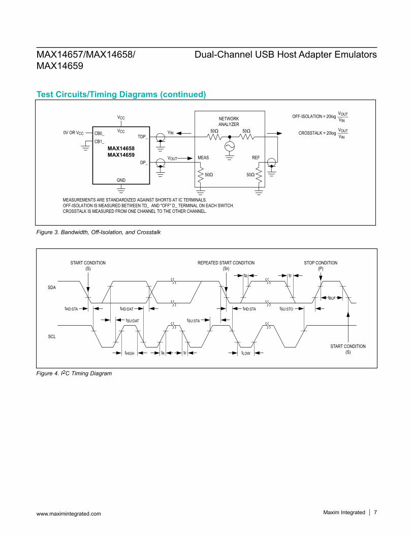
Test Circuits/Timing Diagrams (continued)
Figure 3. Bandwidth, Off-Isolation, and Crosstalk
Figure 4. I2C Timing Diagram
MEASUREMENTS ARE STANDARDIZED AGAINST SHORTS AT IC TERMINALS. OFF-ISOLATION IS MEASURED BETWEEN TD_ AND "OFF" D_ TERMINAL ON EACH SWITCH. CROSSTALK IS MEASURED FROM ONE CHANNEL TO THE OTHER CHANNEL.
VOUT
CB0_ VCC
GND
VCC
TDP_
DP_
VIN
OFF-ISOLATION = 20log VOUT
VIN
CROSSTALK = 20log VOUT
VINCB1_
NETWORKANALYZER
50Ω
50Ω 50Ω
50Ω
MEAS REF
0V OR VCC
MAX14658MAX14659
SDA
START CONDITION(S)
START CONDITION(S)
REPEATED START CONDITION(Sr)
STOP CONDITION(P)
SCL
tHD:STA
tSU:DAT tSU:STA
tHD:DAT tHD:STA tSU:STO
tR tF
tBUF
tHIGH tLOWtR tF

MAX14657/MAX14658/MAX14659
Dual-Channel USB Host Adapter Emulators
Maxim Integrated 8www.maximintegrated.com
Typical Operating Characteristics(VCC = +5V, TA = +25°C, unless otherwise noted.)
USB SWITCH ON-RESISTANCE
MAX
1465
7 to
c01
VTDP/TDM (V)
R ON
(Ω)
42
1
2
3
4
5
00 6
VCC = 5.5V
ITD_ = 10mA
VCC = 3.0V
USB SWITCH ON-RESISTANCE
MAX
1465
7 to
c02
VTDP/TDM (V)
R ON
(Ω)
3.53.02.52.01.51.00.5
2
3
4
5
0
1
0 4.0
VCC = 3.3V, ITD_ = 10mA
TA = -40°CTA = +25°C
TA = +85°C
DP/DM SHORT ON-RESISTANCEvs. VDP
MAX
1465
7 to
c03
VDP (V)
R ON
(Ω)
54321
40
80
120
160
00 6
VCC = 5.5V
IDP = 10mA
VCC = 3.0V
DP/DM SHORT ON-RESISTANCE
MAX
1465
7 to
c04
VDP/DM (V)
R ON
(Ω)
42
20
40
60
80
100
00 6
TA = -40°CTA = +25°C
TA = +85°C
VCC = 5.5V, ID_= 10mA
TDP/DP LEAKAGE CURRENTvs. TEMPERATURE
MAX
1465
7 to
c05
TEMPERATURE (°C)
LEAK
AGE
CURR
ENT
(nA)
35 6010-15
30
60
90
0-40 85
OFF-LEAKAGE
ON-LEAKAGE
VCC = 3.6V, VTDP = 3.3V
VCC (V)
I CC
(µA)
5.04.54.03.5
20
40
60
80
100
120
03.0 5.5
SUPPLY CURRENT vs. SUPPLY VOLTAGE
MAX
1465
7 to
c06
TA = -40°C
TA = +85°C
TA = +25°C
CM MODE
SUPPLY CURRENTvs. LOGIC LEVEL
MAX
1465
7 to
c07
VCB0_ LOGIC LEVEL (V)
I CC
(µA)
3.02.50.5 1.0 1.5 2.0
10
20
30
40
50
60
70
80
00
VCC = 5.5VVCB1_ = 0V
LOGIC-INPUT THRESHOLDvs. SUPPLY VOLTAGE
MAX
1465
7 to
c08
VCC (V)
LOGI
C-IN
PUT
THRE
SHOL
D (V
)
5.04.54.03.5
0.3
0.6
0.9
1.2
03.0 5.5
CB_ FALLING
CB_ RISING

MAX14657/MAX14658/MAX14659
Dual-Channel USB Host Adapter Emulators
Maxim Integrated 9www.maximintegrated.com
Typical Operating Characteristics (continued)(TA = +25°C, unless otherwise noted.)
AUTODETECTION MODE(FROM CM TO AM2 MODE)
MAX14657 toc09
VDP
VDM
VBUS
VSCL
200ms/div
AUTODETECTION MODE(MOUSE PLUGGED IN AM2 MODE)
MAX14657 toc10
VDP
VBUS
400ms/div
DMV
REMOTE WAKE-UP OPERATION(FROM PM/CM TO AM2 MODE WITH
MOUSE PLUGGED IN)MAX14657 toc11
VDP
VDM
VBUS
VSCL
40ms/div
EYE DIAGRAM OFCALIBRATION TRACES
MAX14657 toc12
0.5
0.30.20.1
-0.1-0.2-0.3-0.4-0.5
0
0.4
TIME (x 10^ -9) s
0 0.2
DIFF
EREN
TIAL
SIG
NAL (
V)
0.4 0.6 0.8 1.0 1.2 1.4 1.6 1.8 2.0
EYE DIAGRAMMAX14657 toc13
0.5
0.30.20.1
-0.1-0.2-0.3-0.4-0.5
0
0.4
TIME (x 10^ -9) s
0 0.2
DIFF
EREN
TIAL
SIG
NAL (
V)
0.4 0.6 0.8 1.0 1.2 1.4 1.6 1.8 2.0

MAX14657/MAX14658/MAX14659
Dual-Channel USB Host Adapter Emulators
www.maximintegrated.com Maxim Integrated 10
Pin Descriptions
Pin Configurations
PINNAME FUNCTION
MAX14657 MAX14658 MAX146591 — — SDA I2C Serial Data
— 1 1 CB0A Switch Control Bit. See the switch control input table 1.
2 2 2 VCCPower Supply. Connect a 0.1µF capacitor between VCC and GND as close as possible to the device.
3 3 3 GND Ground
4 — — SAS I2C Slave Address Selection Input
— 4 4 CB0B Switch Control Bit. See the switch control input table 1.
5 — — INT Open-Drain Interrupt Output. INT asserts when interrupt happens.
— 5 5 CB1B Switch Control Bit. See the switch control input table 1.
6 6 6 DPB USB Connector D+ Connection
7 7 7 DMB USB Connector D- Connection
15
16
14
13
5
6
7
GND
SAS
8
SDA
TDMB
TDPB
TDPA
1 3
DMA
4
12 10 9
DPA
SCL EP*
*CONNECT EP TO GROUND PLANE.
CENB
DMB
DPB
INT
V CC
TDMA
2
11
CENA
TQFN(3mm x 3mm)
MAX14657
TOP VIEW
+
15
16
14
13
5
6
7
GND
CB0B
8
CB0A
TDMB
TDPB
TDPA
1 3
DMA
4
12 10 9
DPA
CB1A EP*
CENB
DMB
DPB
CB1B
V CC
TDMA
2
11
CENA
TQFN(3mm x 3mm)
MAX14658
+
15
16
14
13
5
6
7
GND
CB0B
8
CB0A
TDMB
TDPB
TDPA
1 3
DMA
4
12 10 9
DPA
CB1A EP*
CENB
DMB
DPB
CB1B
V CC
TDMA
2
11
CENA
TQFN(3mm x 3mm)
MAX14659
+
MAX14657/MAX14658/MAX14659
Dual-Channel USB Host Adapter Emulators
www.maximintegrated.com Maxim Integrated 11
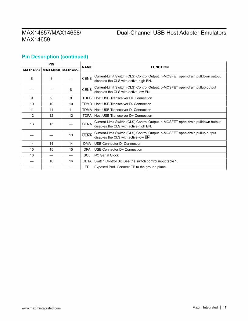
Pin Description (continued)PIN
NAME FUNCTIONMAX14657 MAX14658 MAX14659
8 8 — CENB Current-Limit Switch (CLS) Control Output. n-MOSFET open-drain pulldown output disables the CLS with active-high EN.
— — 8 CENB Current-Limit Switch (CLS) Control Output. p-MOSFET open-drain pullup output disables the CLS with active-low EN.
9 9 9 TDPB Host USB Transceiver D+ Connection
10 10 10 TDMB Host USB Transceiver D- Connection
11 11 11 TDMA Host USB Transceiver D- Connection
12 12 12 TDPA Host USB Transceiver D+ Connection
13 13 — CENA Current-Limit Switch (CLS) Control Output. n-MOSFET open-drain pulldown output disables the CLS with active-high EN.
— — 13 CENA Current-Limit Switch (CLS) Control Output. p-MOSFET open-drain pullup output disables the CLS with active-low EN.
14 14 14 DMA USB Connector D- Connection
15 15 15 DPA USB Connector D+ Connection
16 — — SCL I2C Serial Clock
— 16 16 CB1A Switch Control Bit. See the switch control input table 1.
— — — EP Exposed Pad. Connect EP to the ground plane.

MAX14657/MAX14658/MAX14659
Dual-Channel USB Host Adapter Emulators
www.maximintegrated.com Maxim Integrated 12
Functional Diagram
CONTROL LOGIC
GND
TDM_
CB0A/SDA**
CB0B/SAS**
CB1A/SCL**
TDP_DP_
DM_
VCC
VDP_REFMAX14657MAX14658MAX14659
POR
REF1
DEBOUNCE DCP_REF1
DEBOUNCE
DEBOUNCE
CDP ENGINE
CHAR
GING
DOW
NSTR
EAM
PORT
EMUL
ATIO
N ST
ATE
MACH
INE
DEBOUNCE
DEBOUNCE
DEBOUNCE
DEBOUNCE
VLGC
RDP_CDP
IDP_SINK
VLGC
REF2
REF3
DP
DM1
REF4
REF5
DM2
DM3
500kΩ
RDM_CDP
VDM_SRC
DCP_REF2
CEN_/CEN_*
CB1B/INT**
*CEN IS FOR MAX14659 ONLY.**SDA, SCL, SAS, AND INT ARE FOR MAX14657 ONLY.

MAX14657/MAX14658/MAX14659
Dual-Channel USB Host Adapter Emulators
www.maximintegrated.com Maxim Integrated 13
Detailed DescriptionThe MAX14657/MAX14658/MAX14659 adaptor emulator devices have Hi-Speed USB analog switches that support USB hosts by identifying the USB port as a charger when the USB host is in a low-power mode and cannot enu-merate USB devices. The devices feature low 4pF (typ) on-capacitanceandlow3Ω(typ)on-resistancewhentheUSB switches are connected. DP_ and DM_ are capable of handling signals between 0V and 5.5V over the entire 3.0V to 5.5V supply range.The MAX14657 are controlled by an I2C interface, while the MAX14658/MAX14659 are controlled by the CB0_ and CB1_ logic inputs. The I2C interface allows further customization over which mode the MAX14657 operates in, and can be used to read back connection information.Improvements over the MAX14600 USB detector fam-ily include support for some smart phones that do not connect after applying 0.6V in charging downstream port (CDP) mode. The devices also support high-current charging of Apple devices while in sleep mode.
Enhanced AutomodeThe ICs feature an enhanced automode (AM1, AM2) that allows full charging for Apple devices, USB-compliant devices, and Samsung Galaxy tablets.
Resistor-DividersThe internal voltage buffers with series resistors emulate equivalent resistor-divider networks on the data lines to provide support for Apple/Samsung devices. The voltage buffers are disconnected while not in use to minimize the supply current. The voltage buffers are not connected in pass-through mode. Table 1 summarizes the equivalent resistor values connected to DP_/DM_ in different charg-ing modes.
Switch ControlDigital ControlsEach channel of the MAX14658/MAX14659 features two digital select inputs, CB0_ and CB1_, for mode selection. Table 2 shows how the CB1_/CB0_ inputs can be used to enter Apple 2A auto-detection charger mode (AM2), pass-through mode (PM), forced charger mode (FM), and pass-through mode with CDP emulation (CM).In CDP emulation mode, the peripheral device with CDP detection capability draws charging current up to 1.5A immediately without USB enumeration.
Table 1. DP_/DM_ Resistor-Dividers
Table 2. Digital Input State Table for MAX14658/MAX14659
CHARGING MODE DP_ PULLUP DP_ PULLDOWN DM_ PULLUP DM_ PULLDOWNAM1 75kΩ 49.9kΩ 43.2kΩ 49.9kΩAM2 43.2kΩ 49.9kΩ 75kΩ 49.9kΩ
CB1A/B CB0A/B CHARGER/USB MODE STATUS
0 0 CHARGER AM22A Autodetection Charger Mode. For Apple, Samsung Galaxy tablets, and USB-compliant devices. Voltage buffers emulating Apple 2A resistor-dividers are connected to DP_/DM_.
0 1 USB PM USB Pass-Through Mode. DP_/DM_ are connected to TDP_/TDM_.1 0 CHARGER FM Forced Dedicated Charger Mode. DP_ and DM_ are shorted.
1 1 USB CM USB Pass-Through Mode with CDP Emulation. Autoconnects DP_/DM_ to TDM_/TDM_ depending on CDP detection status.
MAX14657/MAX14658/MAX14659
Dual-Channel USB Host Adapter Emulators
www.maximintegrated.com Maxim Integrated 14
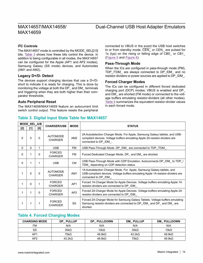
I2C ControlsThe MAX14657 mode is controlled by the MODE_SEL[2:0] bits. Table 3 shows how these bits control the device. In addition to being configurable in all modes, the MAX14657 can be configured for the Apple (AP1 and AP2 modes), Samsung Galaxy (SS mode) devices, and Automodes (AM1 and AM2).
Legacy D+/D- DetectThe devices support charging devices that use a D+/D- short to indicate it is ready for charging. This is done by monitoring the voltage at both the DP_ and DM_ terminals and triggering when they are both higher than their com-parator thresholds.
Auto Peripheral ResetThe MAX14658/MAX14659 feature an autocurrent limit switch control output. This feature resets the peripheral
connected to VBUS in the event the USB host switches to or from standby mode. CEN_ or CEN_ are pulsed for 1s (typ) on the rising or falling edge of CB0_ or CB1_ (Figure 5 and Figure 6).
Pass-Through ModeWhen the ICs are configured in pass-through mode (PM), TDP_/TDM_ are always connected to DP_/DM_ and no resistor-dividers or power sources are applied to DP_/DM_.
Forced Charger ModesThe ICs can be configured in different forced dedicated charging port (DCP) modes; VBUS is enabled and DP_ and DM_ are shorted (FM mode) or connected to the volt-age buffers emulating resistor-dividers (all other modes). Table 4 summarizes the equivalent resistor-divider values in each forced mode.
Table 3. Digital Input State Table for MAX14657
Table 4. Forced Charging Modes
MODE_SEL_A/BCHARGER/USB MODE STATUS
[2] [1] [0]
0 0 0 AUTOMODECHARGER AM2
2A Autodetection Charger Mode. For Apple, Samsung Galaxy tablets, and USB-compliant devices. Voltage buffers emulating Apple 2A resistor-dividers are connected to DP_/DM_.
0 0 1 USB PM USB Pass-Through Mode. DP_/DM_ are connected to TDP_/TDM_.
0 1 0 FORCEDCHARGER FM Forced Dedicated Charger Mode. DP_ and DM_ are shorted.
0 1 1 USB CM USB Pass-Through Mode with CDP Emulation. Autoconnects DP_/DM_ to TDP_/TDM_ depending on CDP detection status.
1 0 0 AUTOMODECHARGER AM1
1A Autodetection Charger Mode. For Apple, Samsung Galaxy tablets, and USB-compliant devices. Voltage buffers emulating Apple 1A resistor-dividers are connected to DP_/DM_.
1 0 1 FORCEDCHARGER AP1 Forced 1A Charger Mode for Apple Devices. Voltage buffers emulating Apple 1A
resistor-dividers are connected to DP_/DM_.
1 1 0 FORCEDCHARGER AP2 Forced 2A Charger Mode for Apple Devices. Voltage buffers emulating Apple 2A
resistor-dividers are connected to DP_/DM_.
1 1 1 FORCEDCHARGER SS
Forced 2A Charger Mode for Samsung Galaxy Tablets. Voltage buffers emulating Samsung resistor-dividers are connected to DP_/DM_ and DP_ and DM_ are shorted.
CHARGING MODE DP_ PULLUP DP_ PULLDOWN DM_ PULLUP DM_ PULLDOWNFM N/A N/A N/A N/ASS 30kΩ 10kΩ 30kΩ 10kΩAP1 75kΩ 49.9kΩ 43.2kΩ 49.9kΩAP2 43.2kΩ 49.9kΩ 75kΩ 49.9kΩ

MAX14657/MAX14658/MAX14659
Dual-Channel USB Host Adapter Emulators
www.maximintegrated.com Maxim Integrated 15
Automatic Detection with Remote Wakeup SupportThe devices feature automatic detection charger mode (AM1/AM2) for dedicated chargers and USB masters. In automatic detection charger mode, the device monitors
the voltages on DM_ and DP_ with voltage buffers con-nected to determine the type of device attached.If a USB-compliant device is connected, DP_ and DM_ are shorted together to commence charging. Once the charging device is removed, the short between DP_ and DM_ is disconnected and the voltage buffer is applied. A pulldown resistor on the shorted DP_/DM_ node ensures that a disconnect is detected.
USB Pass-Through Mode with CDP EmulationThe ICs feature a pass-through mode with CDP emula-tion (CM). This is to support the higher charging current capability during the pass-through mode in normal USB operation (S0 state). The peripheral device equipped with CDP detection capability can draw a charging current as defined in USB battery charger specification 1.2 when the charging host supports the CDP mode. This is a useful feature since most host USB transceivers do not have the CDP function. Table 5 summarizes the USB host power states.
Table 5. USB Host Power States
Figure 5. MAX14659 Peripheral Reset Applications Diagram (CEN is CEN for MAX14658)
Figure 6. MAX14657 Peripheral Reset Applications Diagram
STATE DESCRIPTIONS0 System On
S1Power to the CPU(s) and RAM is maintained; devices that do not indicate they must remain on may be powered down.
S2 CPU is Powered Off
S3Standby (Suspend to Ram): System memory context is maintained, all other system context is lost.
S4 Hibernate: Platform context is maintained.S5 Soft-Off
MAX14659
USBTRANSCEIVER
CURRENT-LIMITSWITCH
PM/AM SYSTEM CONTROL
CM/FMCB1_
CB0_
+5V POWERSUPPLY
VCC
TDM TDP
TDM_ TDP_
0.1µF
150µF
GND
USBCONNECTION
D+DP_
GND
VCC
D-
VBUS
VBUS
DM_
EN
PS EN
CEN_1kΩ
10kΩ
MAX14657
USBTRANSCEIVER
CURRENT-LIMITSWITCH
SYSTEM CONTROL
+5V POWERSUPPLY
VCC
TDM TDP
TDM_ TDP_
0.1µF
150µF
GND
USBCONNECTION
D+DP_
GND
VCC
D-
VBUS
VBUS
DM_
EN
PS EN
SDASDA
INTINT
SASSAS
SCLSCL
CEN_1kΩ
33kΩ
MAX14657/MAX14658/MAX14659
Dual-Channel USB Host Adapter Emulators
www.maximintegrated.com Maxim Integrated 16
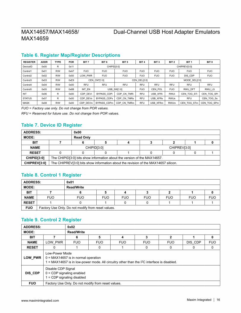
Table 6. Register Map/Register Descriptions
Table 7. Device ID Register
Table 8. Control 1 Register
Table 9. Control 2 Register
FUO = Factory use only. Do not change from POR values.RFU = Reserved for future use. Do not change from POR values.
REGISTER ADDR TYPE POR BIT 7 BIT 6 BIT 5 BIT 4 BIT 3 BIT 2 BIT 1 BIT 0
DeviceID 0x00 R 0x11 CHIPID[3:0] CHIPREV[3:0]
Control1 0x01 R/W 0xA7 FUO FUO FUO FUO FUO FUO FUO FUO
Control2 0x02 R/W 0x50 LOW_PWR FUO FUO FUO FUO FUO DIS_CDP FUO
Control3 0x03 R/W 0xE9 CEN_CNT[1:0] CEN_DEL[2:0] MODE_SEL[2:0]
Control4 0x04 R/W 0x00 RFU RFU RFU RFU RFU RFU RFU RFU
Control5 0x05 R/W 0x6B INT_EN USB_SW[1:0] FUO CEN_POL FUO RWU_DFT RWU_LS
INT 0x06 R 0x00 CDP_DEVi BYPASS_CDPi CDP_CN_TMRi RFU USB_XFRi RWUi CEN_TOG_STi CEN_TOG_SPi
STATUS 0x07 R 0x00 CDP_DEVs BYPASS_CDPs CDP_CN_TMRs RFU USB_XFRs RWUs RFU CEN_TOG_Ss
MASK 0x08 R/W 0x00 CDP_DEVm BYPASS_CDPm CDP_CN_TMRm RFU USB_XFRm RWUm CEN_TOG_STm CEN_TOG_SPm
ADDRESS: 0x00MODE: Read Only
BIT 7 6 5 4 3 2 1 0NAME CHIPID[3:0] CHIPREV[3:0]RESET 0 0 0 1 0 0 0 1
CHIPID[3:0] The CHIPID[3:0] bits show information about the version of the MAX14657.CHIPREV[3:0] The CHIPREV[3:0] bits show information about the revision of the MAX14657 silicon.
ADDRESS: 0x01MODE: Read/Write
BIT 7 6 5 4 3 2 1 0NAME FUO FUO FUO FUO FUO FUO FUO FUORESET 1 0 1 0 0 1 1 1
FUO Factory Use Only. Do not modify from reset values.
ADDRESS: 0x02MODE: Read/Write
BIT 7 6 5 4 3 2 1 0NAME LOW_PWR FUO FUO FUO FUO FUO DIS_CDP FUORESET 0 1 0 1 0 0 0 0
LOW_PWRLow-Power Mode0 = MAX14657 is in normal operation1 = MAX14657 is in low-power mode. All circuitry other than the I2C interface is disabled.
DIS_CDPDisable CDP Signal0 = CDP signaling enabled1 = CDP signaling disabled
FUO Factory Use Only. Do not modify from reset values.

MAX14657/MAX14658/MAX14659
Dual-Channel USB Host Adapter Emulators
www.maximintegrated.com Maxim Integrated 17
Table 10. Control 3 Register
Table 11. Control 4 Register
ADDRESS: 0x03MODE: Read/Write
BIT 7 6 5 4 3 2 1 0NAME CEN_CNT[1:0] CEN_DEL[2:0] MODE_SEL[2:0]RESET 1 1 1 0 1 0 0 1
CEN_CNT[1:0]
CEN_ State Control. Directly controls the CEN_ output independent of automatic cycling.00 = CEN_ asserted 01 = FUO10 = CEN_ deasserted (intend to turn on current-limit switch)11 = CEN_ controlled by CDP/DCP/AM modes
CEN_DEL[2:0]
CEN_ Pulse Delay. Controls how long VBUS toggles last outside of AM mode.000 = 125ms001 = 250ms010 = 350ms011 = 500ms100 = 750ms101 = 1.0s110 = 1.5s111 = 2s
MODE_SEL[2:0]
Operating Mode Control.000 = AM2001 = PM010 = FM011 = CM100 = AM1101 = AP1110 = AP2111 = SS
ADDRESS: 0x04MODE: Read/Write
BIT 7 6 5 4 3 2 1 0NAME RFU RFU RFU RFU RFU RFU RFU RFURESET 0 0 0 0 0 0 0 0
RFU Reserved for Future Use

MAX14657/MAX14658/MAX14659
Dual-Channel USB Host Adapter Emulators
www.maximintegrated.com Maxim Integrated 18
Table 12. Control 5 RegisterADDRESS: 0x05MODE: Read/Write
BIT 7 6 5 4 3 2 1 0NAME INT_EN USB_SW[1:0] FUO CEN_POL FUO RWU_DFT RWU_LSRESET 0 1 1 0 1 0 1 1
INT_ENInterrupt Enable.0 = Interrupt disabled1 = Interrupt enabled
USB_SW[1:0]
USB DPDT Switch Control. When the USB switch is forced open (00) or closed (01), the state machine and CEN_ output are disabled.00 = DP_/DM_ in High-Z01 = DP_/DM_ connected to TDP_/TDM_10 = DP_/DM_ controlled by CDP/DCP/AM circuitry11 = DP_/DM_ controlled by CDP/DCP/AM circuitry
FUO Factory Use Only. Do not modify from reset value.
CEN_POLCEN Polarity Select. Controls the polarity of the CEN output.0 = CEN output is active-low CEN1 = CEN output is active-high CEN
FUO Factory Use Only. Do not modify from reset value.
RWU_DFTRemote Wake-Up Default0 = Remote wake-up is off1 = Remote wake-up is on
RWU_LSRemote Wake-Up for Low-Speed Only Select0 = Remote wake-up for both FS/HS and LS USB devices1 = Remote wake-up for only LS devices

MAX14657/MAX14658/MAX14659
Dual-Channel USB Host Adapter Emulators
www.maximintegrated.com Maxim Integrated 19
Table 13. Interrupt RegisterADDRESS: 0x06MODE: Read Only
BIT 7 6 5 4 3 2 1 0NAME CDP_DEVi BYPASS_CDPi CDP_CNi RFU USB_XFRi RWUi CEN_TOG_STi CEN_TOG_SPiRESET 0 0 0 0 0 0 0 0
CDP_DEVi
CDP Device Detect Status Interrupt. CDP_DEVi is set when a CDP device is detected following the CDP handshake procedure in CM mode.0 = No interrupt1 = Interrupt
BYPASS_CDPiBypass CDP Running Status Interrupt. BYPASS_CDPi is set when the CDP handshake procedure is bypassed.0 = No interrupt1 = Interrupt
CDP_CNiCDP Connect Status Interrupt. CDP_CNi is set whenever a CDP connection check is in progress.0 = No interrupt1 = Interrupt
RFU Reserved for Future Use
USB_XFRi
USB Session Interrupt. USB_XFRi is set when there is USB data detected in CM mode and DP_/DM_ are connected to TDP/TDM.0 = No interrupt1 = Interrupt
RWUiRemote Wake-Up Status Interrupt. RWUi is set whenever a remote wake-up is performed in AM mode.0 = No interrupt1 = Interrupt
CEN_TOG_STi
CEN_ Toggle Start Monitor Interrupt. CEN_TOG_STi is set at the start of a VBUS toggle, when VBUSisfirstdisabled.0 = No interrupt1 = Interrupt
CEN_TOG_SPi
CEN_ Toggle Stop Monitor Interrupt. CEN_TOG_SPi is set at the end of a VBUS toggle, when VBUS is no longer disabled.0 = No interrupt1 = Interrupt

MAX14657/MAX14658/MAX14659
Dual-Channel USB Host Adapter Emulators
www.maximintegrated.com Maxim Integrated 20
Table 14. Status RegisterADDRESS: 0x07MODE: Read Only
BIT 7 6 5 4 3 2 1 0NAME CDP_DEVs BYPASS_CDPs CDP_CNs RFU USB_XFRs RWUs RFU CEN_TOGsRESET 0 0 0 0 0 0 0 0
CDP_DEVs
CDP Device Detect Status. CDP_DEVs is set when a CDP device is detected following the CDP handshake procedure in CM mode and cleared when it is disconnected.0 = CDP device not detected1 = CDP device detected
BYPASS_CDPsBypass CDP Running Status. BYPASS_CDPs is set when the CDP handshake procedure is bypassed.0 = CDP signaling used1 = CDP signaling bypassed
CDP_CNsCDP Connect Status. CDP_CNs is set while a CDP connection attempt is in progress.0 = No CDP connection check in progress1 = CDP connection check in progress
RFU Reserved for Future Use
USB_XFRs
USB Session Status. USB_XFRs is set while there is USB data detected in CM mode and DP_/DM_ are connected to TDP/TDM.0 = No USB session in progress1 = USB session in progress
RWUsRemote Wake-Up Status. RWUs is set while a remote wake-up is in progress in AM mode.0 = Not waiting for RWU1 = Waiting for RWU
CEN_TOGs
CEN_ Toggle Status. CEN_TOGs is cleared at the start of a VBUS toggle and set at the end of the VBUS toggle.0 = VBUS toggle in progress1 = VBUS toggle not in progress

MAX14657/MAX14658/MAX14659
Dual-Channel USB Host Adapter Emulators
www.maximintegrated.com Maxim Integrated 21
Table 15. Mask RegisterADDRESS: 0x08MODE: Read/Write
BIT 7 6 5 4 3 2 1 0
NAME CDP_ DEVm
BYPASS_ CDPm CDP_CNm RFU USB_XFRm RWUm CEN_TOG_
STmCEN_TOG_
SPmRESET 0 0 0 0 0 0 0 0
CDP_DEVm
CDP Device Detect Status Interrupt Mask. Prevents an interrupt from being generated in CDP_DEVi when CDP_DEVs is set to 1.0 = Masked1 = Not masked
BYPASS_CDPm
Bypass CDP Running Status Interrupt Mask. Prevents an interrupt from being generated in BYPASS_CDPi when BYPASS_CDPs is set to 1.0 = Masked1 = Not masked
CDP_CNm
CDP Connect Status Interrupt Mask. Prevents an interrupt from being generated in CDP_CNi when CDP_CNs is set to 1.0 = Masked1 = Not masked
RFU Reserved for Future Use
USB_XFRm
USB Session Interrupt Mask. Prevents an interrupt from being generated in USB_XFRi when USB_XFRs is set to 1.0 = Masked1 = Not masked
RWUm
Remote Wake-Up Status Interrupt Mask. Prevents an interrupt from being generated in RWUi when RWUs is set to 1.0 = Masked1 = Not masked
CEN_TOG_STm
CEN_ Toggle Start Monitor Interrupt Mask. Prevents an interrupt from being generated in CEN_TOG_STi when CEN_TOG_STs is set to 1.0 = Masked1 = Not masked
CEN_TOG_SPm
CEN_ Toggle Stop Monitor Interrupt Mask. Prevents an interrupt from being generated in CEN_TOG_SPi when CEN_TOG_SPs is set to 1.0 = Masked1 = Not masked

MAX14657/MAX14658/MAX14659
Dual-Channel USB Host Adapter Emulators
www.maximintegrated.com Maxim Integrated 22
Applications InformationI2C InterfaceThe MAX14657 contain an I2C-compatible interface for data communication with a host controller (SCL and SDA). The interface supports a clock frequency of up to 400kHz. SCL and SDA require pullup resistors that are connected to a positive supply.
Start, Stop, and Repeated Start ConditionsWhen writing to the MAX14657 using I2C, the master sends a START condition (S) followed by the MAX14657 I2C address. After the address, the master sends the register address of the register that is to be programmed. The master then ends communication by issuing a STOP condition (P) to relinquish control of the bus, or a Repeated START condition (Sr) to communicate to another I2C slave. See Figure 7.
Slave AddressThe MAX14657 is the I2C version that has different slave addresses for each port (Table 16). Set the Read/Write bit high to configure the MAX14657 to read mode. Set the Read/Write bit low to configure the MAX14657 to write mode. Further, two possible slave addresses can be configured for each port through the Slave Address Selection (SAS) input (see Table 16), allowing up to two MAX14657 devices to share the same interface bus. The address is the first byte of information sent to the MAX14657 after the START condition.
Bit TransferOne data bit is transferred on the rising edge of each SCL clock cycle. The data on SDA must remain stable during the high period of the SCL clock pulse. Changes in SDA while SCL is high and stable are considered control sig-nals (see the Start, Stop, and Repeated Start Conditions section). Both SDA and SCL remain high when the bus is not active.
Figure 7. I2C START, STOP, and REPEATED START Conditions
Table 16. MAX14657 I2C Slave AddressesSAS Port A6 A5 A4 A3 A2 A1 A0 R/W READ ADDR WRITE ADDR
GNDA 0 1 0 0 1 0 0 1/0 0x49 0x48B 0 1 0 1 1 0 0 1/0 0x59 0x58
VCCA 0 1 0 0 1 0 1 1/0 0x4B 0x4AB 0 1 0 1 1 0 1 1/0 0x5B 0x5A
SCL
SDA
S Sr P

MAX14657/MAX14658/MAX14659
Dual-Channel USB Host Adapter Emulators
www.maximintegrated.com Maxim Integrated 23
Single Byte WriteIn this operation, the master sends an address and two data bytes to the slave device (Figure 8). The following procedure describes the single byte write operation:1) The master sends a START condition2) The master sends the 7-bit slave address plus a write
bit (low)3) The addressed slave asserts an ACK on the data line4) The master sends the 8-bit register address5) The slave asserts an ACK on the data line only if the
address is valid (NAK if not)6) The master sends 8 data bits7) The slave asserts an ACK on the data line8) The master generates a STOP condition
Burst WriteIn this operation, the master sends an address and mul-tiple data bytes to the slave device (Figure 9). The slave device automatically increments the register address after each data byte is sent, unless the register being accessed is 0x00, in which case the register address remains the same. The following procedure describes the burst write operation:1) The master sends a START condition2) The master sends the 7-bit slave address plus a write
bit (low)3) The addressed slave asserts an ACK on the data line4) The master sends the 8-bit register address5) The slave asserts an ACK on the data line only if the
address is valid (NAK if not)6) The master sends 8 data bits7) The slave asserts an ACK on the data line8) Repeat 6 and 7 (N-1) times9) The master generates a STOP condition
Figure 8. Write Byte Sequence
Figure 9. Burst Write Sequence
S
P
DEVICE SLAVE ADDRESS - W A
8 DATA BITS
FROM MASTER TO SLAVE
WRITE SINGLE BYTE
FROM SLAVE TO MASTER
A
REGISTER ADDRESS A
S DEVICE SLAVE ADDRESS - W A
8 DATA BITS - 1
BURST WRITE
A
REGISTER ADDRESS A
8 DATA BITS - N A
8 DATA BITS - 2 A
FROM MASTER TO SLAVE FROM SLAVE TO MASTER
P

MAX14657/MAX14658/MAX14659
Dual-Channel USB Host Adapter Emulators
www.maximintegrated.com Maxim Integrated 24
Single Byte ReadIn this operation, the master sends an address plus two data bytes and receives one data byte from the slave device (Figure 10). The following procedure describes the single byte read operation:1) The master sends a START condition2) The master sends the 7-bit slave address plus a write
bit (low)3) The addressed slave asserts an ACK on the data line4) The master sends the 8-bit register address5) The slave asserts an ACK on the data line only if the
address is valid (NAK if not)6) The master sends a REPEATED START condition7) The master sends the 7-bit slave address plus a read
bit (high)8) The addressed slave asserts an ACK on the data line9) The slave sends 8 data bits
10) The master asserts a NACK on the data line11) The master generates a STOP condition
Burst ReadIn this operation, the master sends an address plus two data bytes and receives multiple data bytes from the slave device (Figure 11). The following procedure describes the burst byte read operation:1) The master sends a START condition2) The master sends the 7-bit slave address plus a write
bit (low)3) The addressed slave asserts an ACK on the data line4) The master sends the 8-bit register address5) The slave asserts an ACK on the data line only if the
address is valid (NAK if not)6) The master sends a REPEATED START condition7) The master sends the 7-bit slave address plus a read
bit (high)
Figure 10. Read Byte Sequence
Figure 11. Burst Read Sequence
S
Sr
DEVICE SLAVE ADDRESS - W A
DEVICE SLAVE ADDRESS - R
READ SINGLE BYTE
A
REGISTER ADDRESS A
8 DATA BITS NA
FROM MASTER TO SLAVE FROM SLAVE TO MASTER
P
S
Sr
DEVICE SLAVE ADDRESS - W A
DEVICE SLAVE ADDRESS - R
BURST READ
A
REGISTER ADDRESS A
8 DATA BITS - 1 A
A 8 DATA BITS - 38 DATA BITS - 2 A
8 DATA BITS - N NA
FROM MASTER TO SLAVE FROM SLAVE TO MASTER
P

MAX14657/MAX14658/MAX14659
Dual-Channel USB Host Adapter Emulators
www.maximintegrated.com Maxim Integrated 25
8) The slave asserts an ACK on the data line9) The slave sends 8 data bits10) The master asserts an ACK on the data line11) Repeat 9 and 10 (N-2) times12) The slave sends the last 8 data bits13) The master asserts a NACK on the data line14) The master generates a STOP condition
Acknowledge BitsData transfers are acknowledged with an acknowledge bit (ACK) or a not-acknowledge bit (NACK). Both the master and the MAX14657 generate ACK bits. To generate an ACK, pull SDA low before the rising edge of the ninth clock pulse and hold it low during the high period of the ninth clock pulse (see Figure 12). To generate a NACK,
leave SDA high before the rising edge of the ninth clock pulse and leave it high for the duration of the ninth clock pulse. Monitoring for NACK bits allows for detection of unsuccessful data transfers.
High ESD ProtectionElectrostatic discharge (ESD) protection structures are incorporated on all pins to protect against electrostatic discharges up to ±2kV Human Body Model (HBM) encountered during handling and assembly. DP_ and DM_ are further protected against high ESD up to ±15kV (HBM) without damage. These ESD structures withstand high ESD both in normal operation and when the device is powered down. After an ESD event, the IC continues to function without latchup.
ESD Test ConditionsESD performance depends on a variety of conditions. Contact Maxim for a reliability report that documents test setup, test methodology, and test results.
Human Body ModelFigure 13 shows the Human Body Model. Figure 14 shows the current waveform it generates when discharged into a low impedance. This model consists of a 100pF capacitor charged to the ESD voltage of interest that is then dis-chargedintothedevicethrougha1.5kΩresistor.
Figure 12. Acknowledge
Figure 13. Human Body ESD Test Model Figure 14. Human Body Current Waveform
100%
36.8%
tRL
TIME
tDL
PEAK-TO-PEAK RINGING(NOT DRAWN TO SCALE)Ir
00
IPEAK (AMPS)
90%
10%
NOT ACKNOWLEDGE
ACKNOWLEDGE
1 2 8 9
SDA
SCL
S
CHARGE-CURRENT-LIMIT RESISTOR
DISCHARGERESISTANCE
STORAGECAPACITOR
CS100pF
RC1MΩ
RD1.5kΩ
HIGH- VOLTAGE
DCSOURCE
DEVICEUNDERTEST

MAX14657/MAX14658/MAX14659
Dual-Channel USB Host Adapter Emulators
www.maximintegrated.com Maxim Integrated 26
Package InformationFor the latest package outline information and land patterns (footprints), go to www.maximintegrated.com/packages. Note that a “+”, “#”, or “-” in the package code indicates RoHS status only. Package drawings may show a different suffix character, but the drawing pertains to the package regardless of RoHS status.
Chip InformationPROCESS: BiCMOS
+Denotes a lead(Pb)-free/RoHS-compliant package.*EP = Exposed pad.T = Tape and reel.
Ordering Information
Typical Operating Circuit
PART TEMP RANGE PIN-PACKAGEMAX14657ETE+T -40°C to +85°C 16 TQFN-EP*MAX14658ETE+T -40°C to +85°C 16 TQFN-EP*MAX14659ETE+T -40°C to +85°C 16 TQFN-EP*
PACKAGE TYPE
PACKAGE CODE
OUTLINE NO.
LAND PATTERN NO.
16 TQFN T1633+5 21-0136 90-0032
DMA
CENA/B
D-
DPA
DMB
DPB
D+
VBUS
+5VA
+5VA
+5V
GND
Li+BATTERY
EXTERNALPOWERSUPPLY
5VSWITCHING
POWER SUPPLY
USB A
+5VB
CLS
CLS
APPL
E DO
CKCO
NNEC
TOR
APPL
E DO
CK
iPad® OR iPhone®
USB A MICRO B
MICR
O-US
BCO
NNEC
TOR
PHONE OR MP3PLAYER
TDMA
TDPA
SASLAPTOP CHIPSET
EC
USBTRANSCEIVER
TDMB
TDPB
SCLSDA
INT
USBTRANSCEIVER
MAX14657 USB
A CO
NNEC
TOR
D-
D+
VBUS
+5VB
GND
USB
A CO
NNEC
TOR
INT

Maxim Integrated cannot assume responsibility for use of any circuitry other than circuitry entirely embodied in a Maxim Integrated product. No circuit patent licenses are implied. Maxim Integrated reserves the right to change the circuitry and specifications without notice at any time. The parametric values (min and max limits) shown in the Electrical Characteristics table are guaranteed. Other parametric values quoted in this data sheet are provided for guidance.
Maxim Integrated and the Maxim Integrated logo are trademarks of Maxim Integrated Products, Inc.
MAX14657/MAX14658/MAX14659
Dual-Channel USB Host Adapter Emulators
© 2013 Maxim Integrated Products, Inc. 27
Revision HistoryREVISION NUMBER
REVISION DATE DESCRIPTION PAGES
CHANGED0 4/13 Initial release —1 8/13 Updated Ordering Information 26
For pricing, delivery, and ordering information, please contact Maxim Direct at 1-888-629-4642, or visit Maxim Integrated’s website at www.maximintegrated.com.

Mouser Electronics
Authorized Distributor
Click to View Pricing, Inventory, Delivery & Lifecycle Information: Maxim Integrated:
MAX14658ETE+T MAX14657ETE+T MAX14659ETE+T