CYPD3184, USB PD power adapter SR controller
28
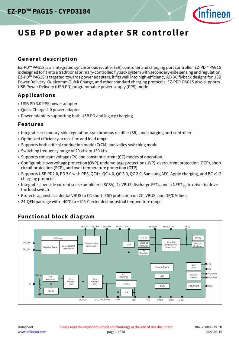
Datasheet Please read the Important Notice and Warnings at the end of this document 002-26809 Rev. *D www.infineon.com page 1 of 28 2022-06-16 EZ-PD™ PAG1S - CYPD3184 USB PD power adapter SR controller General description EZ-PD™ PAG1S is an integrated synchronous rectifier (SR) controller and charging port controller. EZ-PD™ PAG1S is designed to fit into a traditional primary-controlled flyback system with secondary-side sensing and regulation. EZ-PD™ PAG1S is targeted towards power adapters, it fits well into high-efficiency AC-DC flyback designs for USB Power Delivery, Qualcomm Quick Charge, and other standard charging protocols. EZ-PD™ PAG1S also supports USB Power Delivery (USB PD) programmable power supply (PPS) mode. Applications • USB PD 3.0 PPS power adapter • Quick Charge 4.0 power adapter • Power adapters supporting both USB PD and legacy charging Features • Integrates secondary-side regulation, synchronous rectifier (SR), and charging port controller • Optimized efficiency across line and load range • Supports both critical conduction mode (CrCM) and valley switching mode • Switching frequency range of 20 kHz to 150 kHz • Supports constant voltage (CV) and constant current (CC) modes of operation. • Configurable overvoltage protection (OVP), undervoltage protection (UVP), overcurrent protection (OCP), short circuit protection (SCP), and over-temperature protection (OTP) • Supports USB PD2.0, PD 3.0 with PPS, QC4+, QC 4.0, QC 3.0, QC 2.0, Samsung AFC, Apple charging, and BC v1.2 charging protocols • Integrates low-side current sense amplifier (LSCSA), 2x VBUS discharge FETs, and a NFET gate driver to drive the load switch • Protects against accidental VBUS to CC short; ESD protection on CC, VBUS, and DP/DM lines • 24-QFN package with –40°C to +105°C extended industrial temperature range Functional block diagram CC2 DP_GPIO5 XRES DM_GPIO4 VBUS_CTRL Charger Detect VBUS_C CC1 Slew Rate Controlled NFET Gate Driver CSN BMC PHY VBUS_IN HV Regulator VBUS_C Discharge LDO VDDD VCCD GPIO0 GPIO1 SR_SEN SR_GDRV SR_CPP SR_CPN FB VSS CC_COMP_GPIO2 OV, UV VBUS_IN Discharge OV, UV ADC GPIOs POR/RESET LSCSA SCP CC Reference CSP Error Amplifier (CC) Error Amplifier (CV) CV Reference IDACs EA_OUT V Negative Sense Zero Crossing Detect (ZCD) SR Sense SR_VSS SR Gate Driver and Doubler VBUS_IN V V V V V GPIO3 Protocol Engine
-
Upload
khangminh22 -
Category
Documents
-
view
3 -
download
0
Transcript of CYPD3184, USB PD power adapter SR controller
Datasheet Please read the Important Notice and Warnings at the end of this document 002-26809 Rev Dwwwinfineoncom page 1 of 28 2022-06-16
EZ-PDtrade PAG1S - CYPD3184
US B PD power adapter SR controller
General descriptionEZ-PDtrade PAG1S is an integrated synchronous rectifier (SR) controller and charging port controller EZ-PDtrade PAG1S is designed to fit into a traditional primary-controlled flyback system with secondary-side sensing and regulation EZ-PDtrade PAG1S is targeted towards power adapters it fits well into high-efficiency AC-DC flyback designs for USB Power Delivery Qualcomm Quick Charge and other standard charging protocols EZ-PDtrade PAG1S also supports USB Power Delivery (USB PD) programmable power supply (PPS) mode
Applicationsbull USB PD 30 PPS power adapterbull Quick Charge 40 power adapterbull Power adapters supporting both USB PD and legacy charging
Featuresbull Integrates secondary-side regulation synchronous rectifier (SR) and charging port controllerbull Optimized efficiency across line and load rangebull Supports both critical conduction mode (CrCM) and valley switching modebull Switching frequency range of 20 kHz to 150 kHzbull Supports constant voltage (CV) and constant current (CC) modes of operation bull Configurable overvoltage protection (OVP) undervoltage protection (UVP) overcurrent protection (OCP) short
circuit protection (SCP) and over-temperature protection (OTP)bull Supports USB PD20 PD 30 with PPS QC4+ QC 40 QC 30 QC 20 Samsung AFC Apple charging and BC v12
charging protocolsbull Integrates low-side current sense amplifier (LSCSA) 2x VBUS discharge FETs and a NFET gate driver to drive
the load switchbull Protects against accidental VBUS to CC short ESD protection on CC VBUS and DPDM lines bull 24-QFN package with ndash40degC to +105degC extended industrial temperature range
Functional block diagram
CC2
DP_GPIO5
XRES
DM_GPIO4
VBUS_CTRL
Charger Detect
VBUS_C
CC1
Slew Rate Controlled NFET
Gate Driver
CSN
BMCPHY
VBUS_IN
HVRegulator
VBUS_C Discharge
LDO
VDDD VCCD
GPIO0 GPIO1
SR_SEN
SR_GDRVSR_CPP SR_CPN
FB
VSSCC_COMP_GPIO2
OV UV
VBUS_IN Discharge
OV UV
ADC
GPIOs PORRESETLSCSA
SCP
CC Reference
CSP
Error Amplifier
(CC)
Error Amplifier
(CV)
CV Reference
IDACs
EA_OUT
V
Negative Sense Zero Crossing Detect (ZCD)
SR Sense
SR_VSS SR Gate Driver and Doubler
VBUS_IN
V
V
VV
V
GPIO3
Protocol Engine
Datasheet 2 of 28 002-26809 Rev D2022-06-16
USB PD power adapter SR controller
Table of contents
Table of contentsGeneral description 1Applications1Features 1Functional block diagram1Table of contents 21 Pinout311 Pin description 52 Application overview 921 USB Power Delivery power adapter93 Functional description 1031 Start-up behavior1032 Fault protection 1033 Power modes 104 Electrical specifications1141 Absolute maximum ratings 1142 Device-level specifications 1243 Functional block specifications 1344 IO specifications 1945 System resources specifications 205 Ordering information 2151 Ordering code definitions216 Packaging 227 Acronyms 248 Document conventions2681 Units of measure 26Revision history 27
Datasheet 3 of 28 002-26809 Rev D2022-06-16
USB PD power adapter SR controller
Pinout
1 Pinout
Figure 1 24-pin QFN pin map
1
2
3
4
5
6
SR_VSS
SR_SEN
XRES
GPIO0
GPIO1
7 8 9 10 11 12
CC_C
OM
P_GP
IO2
EA_O
UT FB
CSN
CSP
GPIO
3
18
17
16
15
14
13
VBUS_C
DP_GPIO5
DM_GPIO4
VSS
CC1
CC2
24 23 22 21 20 19
SR_C
PP
SR_C
PN
VDDD
VCCD
VBU
S_IN
VBU
S_CT
RL
EPAD
SR_GDRV
Datasheet 4 of 28 002-26809 Rev D2022-06-16
USB PD power adapter SR controller
Pinout
Table 1 EZ-PDtrade PAG1S pin descriptionPin number Pin name Description
1 SR_GDRV Synchronous-rectifier NFET gate driver2 SR_VSS Synchronous-rectifier NFET ground terminal3 SR_SEN Synchronous-rectifier NFET drain terminal4 XRES External reset input5 GPIO0 GPIO P006 GPIO1 GPIO P017 CC_COMP_GPIO2 Pin for constant current mode compensation capacitorGPIO P028 EA_OUT Error amplifier output9 FB Error amplifier feedback
10 CSN Low-side current sense amplifier negative input11 CSP Low-side current sense amplifier positive input12 GPIO3 GPIO P0313 CC2 Power Delivery communication channel 214 CC1 Power Delivery communication channel 115 VSS Ground16 DM_GPIO4 USB D-SWD_DATAGPIO P0417 DP_GPIO5 USB D+SWD_CLKGPIO P0518 VBUS_C USB Type-C VBUS monitor input19 VBUS_CTRL Load switch NFET gate control20 VBUS_IN Power source input21 VCCD 18-V core voltage LDO output22 VDDD 30 Vndash55 V internal LDO Output23 SR_CPN SR doubler capacitor negative pin24 SR_CPP SR doubler capacitor positive pin 25 EPAD EPAD for ground
Datasheet 5 of 28 002-26809 Rev D2022-06-16
USB PD power adapter SR controller
Pinout
11 Pin descriptionSR_GDRV SR_VSS SR_SEN SR_CPP SR_CPN EZ-PDtrade PAG1S senses the voltage across the SR NFET and appropriately controls the gate driver to achieve optimum efficiency The gate driver (SR_GDRV) can be driven to internal VDDD or twice of VDDD to achieve better RDS-On of the external NFET The Gate Driver can be driven to twice of VDDD using an internal doubler circuit with the doubler capacitor connected across SR_CPP and SR_CPN pins The source terminal of the SR FET shall be connected to SR_VSS pin EZ-PDtrade PAG1S supports SR in QRCrCM and valley switching The SR sense block supports negative sense detect and Zero Crossing Detect (ZCD) The voltage at the drain node of the external NFET is sensed using a resistive divider The internal resistor is 2 k the external resistor needs to be chosen such that the voltage at the SR_SEN pin does not exceed 215 V The external resistance on SR_SEN pin depends on turns ratio of power transformer Table 2 provides the values required for various values of turns ratio
The fast-negative sense comparator can detect a minimum negative voltage of 100 mV to ndash200 mV on SR_SEN pin Similarly ZCD can detect a minimum threshold of ndash16 mV to 0 mV on the SR_SEN pin See Figure 2 and Figure 3 for the waveforms representing the SR_GDRV functionality in CrCM and valley switching mode
Table 2 External resistance on SR_SEN vs turns ratioPrimary Secondary turns ratio Rext ()
41 10K51 9K61 8K71 7K81 6K91 5K
101 4K
Datasheet 6 of 28 002-26809 Rev D2022-06-16
USB PD power adapter SR controller
Pinout
Figure 2 SR_SEN and SR_GDRV in QRCrCM mode
Time
Primary Current
Secondary Current
SR_SEN
Primary FET ON SR FET OFF
Primary FET ON SR FET OFF
Primary FET OFF SR FET ON
Primary FET OFF SR FET ON
Feed forward sensing
Negative sense detect
ZCDPeak detect
Both FET OFF
SR_GDRV
Datasheet 7 of 28 002-26809 Rev D2022-06-16
USB PD power adapter SR controller
Pinout
Figure 3 SR_SEN and SR_GDRV in valley switching mode
111 FB EA_OUT CC_COMP_GPIO2EZ-PDtrade PAG1S integrates two error amplifier blocks which handles secondary output sensing and regulation for CV and CC modes This block is responsible for both constant voltage and constant current operations The output of the error amplifier is routed to the EA_OUT pin EA_OUT can further drive an opto-isolator to provide feedback to the primary controller The negative input of the error amplifier is the feedback (FB) pin and the positive input is internal reference of 0744 V The FB pin has internal resistor divider of 200 k and 35 k this divider sets a default voltage of 0744 V at FB pin when VBUS_IN is at 5V Based on the desired VBUS_C output the voltage at the FB pin will be varied using internal current sourcesink IDACs An external compensation network is required between FB pin and EA_OUT pin as shown in Figure 4 Constant current operation makes use of an internal LSCSA the output of which feeds into an independent error amplifier as shown in Figure 4 EZ-PDtrade PAG1S error amplifier can ensure constant voltage regulation over 33 V to 215 V range and constant current regulation over 1 A to 3 A as required by the USB PD PPS specification
112 CC1 CC2CC1 and CC2 are the communication channels for USB PD protocol EZ-PDtrade PAG1S integrates a USB PD transceiver consisting of a transmitter and receiver that communicate biphase mark code (BMC) encoded data over the configuration channel (CC) channels as per the USB PD standard All communication is half-duplex The physical layer implements collision avoidance to minimize communication errors on the channel This block includes all termination resistors (Rp) and their switches as required by the USB PD specification An external 390-pF capacitor is required on both the CC1 and CC2 pins
Time
Primary Current
Secondary Current
SR_SEN
Primary FET ON SR FET OFF
Primary FET ON SR FET OFF
Primary FET OFF SR FET ON
Primary FET OFF SR FET ON
Feed forward sensing
Negative sense detect
ZCD
Both FET OFF
SR_GDRV
Valley detect
Datasheet 8 of 28 002-26809 Rev D2022-06-16
USB PD power adapter SR controller
Pinout
113 DP_GPIO4 DM_GPIO5The DP and DM lines are the standard USB D+ and Dndash lines EZ-PDtrade PAG1S integrates a charge detect block which handles legacy charging protocols such as BC 12 Quick Charge Apple charging and Samsung AFC This block integrates all the terminations required for these charging protocols and no external components are required When legacy charging is not required in the system the same DP and DM lines can be reused as standard GPIOs
114 VBUS_IN VDDD VCCDEZ-PDtrade PAG1S integrates a high-voltage regulator which is powered from the VBUS_IN rail the output of the regulator powers the VDDD rail The input to the regulator can range from 33 V minimum to 215 V maximum When the input is between 55 V to 215 V the typical output of the regulator is 5 V For inputs from 33 V to 55 V the regulator output is VBUS_IN ndash 300 mV The regulator can drive a maximum load current of 50 mA which includes the chip current consumption This regulator is not expected to drive any external loads or ICs EZ-PDtrade PAG1S also has an internal configurable discharge path for the VBUS_IN rail which is used to discharge the VBUS rail during negative voltage transitionsThe regulated supply VDDD is either used to directly power some internal analog blocks or further regulated down to 18 V VCCD which powers majority of the core VDDD and VCCD is brought out on to pins to connect external capacitors for regulator stability these are not meant to be used as power supplies
115 VBUS_C VBUS_CTRLVBUS_C is used to monitor the voltage at the Type-C connector VBUS_C has an internal configurable discharge path which is used to discharge the VBUS_C rail during negative voltage transitionsThe load switch is between VBUS_IN and VBUS_C EZ-PDtrade PAG1S integrates a NFET gate driver to control this load switch VBUS_CTRL is the output of this gate driver To turn off the external NFET the gate driver drives low To turn on the external NFET it drives the gate to VBUS_IN + 8 V In addition there is a clamp circuit to limit the gate to VBUS_IN + 8 V
116 CSP CSNEZ-PDtrade PAG1S integrates a LSCSA to monitor the load current CSP is the positive input pin for the LSCSA and CSN is the negative input LSCSA offers wide gain options ranging from 5 to 150 Suggested Rsense for LSCSA is 5 m LSCSA has an active offset cancellation mechanism to improve accuracy
117 GPIO0 GPIO1 and GPIO3EZ-PDtrade PAG1S has six GPIOs out of which three are dedicated GPIOs and the rest are multiplexed with other functionalities During power-on and reset the IO pins (except GPIO1) are forced to the tristate so as not to crowbar any inputs andor cause excess turn-on current GPIO1 is driven to zero at power-up
118 XRESThe XRES pin can be used to initiate a reset this pin is internally pulled high and needs to be pulled low externally to trigger reset
Datasheet 9 of 28 002-26809 Rev D2022-06-16
USB PD power adapter SR controller
Application overview
2 Application overview
21 USB Power Delivery power adapterFigure 4 shows a power adapter application diagram implementing a primary side controlled synchronous flyback system In this system EZ-PDtrade PAG1S engages the error amplifier to take the feedback from the secondary side and pass it on to the primary controller over an isolation barrier like an opto-isolator The primary side controller can be any standard flyback controller In this topology EZ-PDtrade PAG1S integrates three key features secondary side sensing and regulation SR and charging port controller
Figure 4 Power adapter with primary side control application diagram
Primary Flyback
Controller
Secondary Side
Isol
atio
n Ba
rrie
r
Primary Side
EMI Filter
Full-bridge Rectifier Snubber
GND
VDD700
GD
CS
FB
USB
Typ
e-C
Conn
ecto
r
CC1
CC2
DP_GPIO5
DM_GPIO4
VBUS_TypeC
EZ-PD PAG1SSR
_VSS
SR_G
DRV
SR_S
EN
GPIO1
SR_C
PP
SR_C
PN
VBUS
_IN
VBU
S_CT
RL
CSN
CSP
VBU
S_C
VDDD
VCCD
VBUS_IN
Temperature Sensor
GPIO0
CC_COMP_GPIO2
EA_OUT
FB
AC In
put
Datasheet 10 of 28 002-26809 Rev D2022-06-16
USB PD power adapter SR controller
Functional description
3 Functional description
31 Start-up behaviorOn power-up the primary side flyback controller shall start controlling the primary switch using its internal primary peak current limited soft start mechanism and provide sufficient current to charge the secondary side output capacitor and the startup current required for EZ-PDtrade PAG1S The secondary output voltage is the input power supply source of EZ-PDtrade PAG1S Once this voltage at VBUS_IN crosses 33 V EZ-PDtrade PAG1S gets powered up EZ-PDtrade PAG1S firmware boot-up time is in the order of a few milliseconds Once the boot-up is complete EZ-PDtrade PAG1S configures the error-amplifier to achieve 5 V secondary output The output of the error-amplifier is passed on to the primary controller through an opto-coupler
32 Fault protection
321 VBUS UVP and OVPVBUS undervoltage and overvoltage faults are monitored using internal VBUS_INVBUS_C resistor dividers The fault thresholds and response times are configurable in EZ-PDtrade PAG1S Configurability includes choosing between auto-restart or latch-off options for each fault
322 VBUS OCP and SCPVBUS overcurrent and short-circuit faults are monitored using internal current sense amplifiers Same as OVP and UVP the OCP and SCP fault thresholds and response times are configurable as well Configurability includes choosing between auto-restart or latch-off options for each fault
323 OTPOvertemperature monitoring is done using an external thermistor and internal ADC The thermistor can be connected to any free GPIO
324 ESD protectionEZ-PDtrade PAG1S offers ESD protection on all the pins The ESD protection level is 22-kV HBM and 500-V CDM
325 VBUS to CC short protectionEZ-PDtrade PAG1S offers protection against accidental short from VBUS_C pin short to CC
33 Power modesEZ-PDtrade PAG1S supports three power modes - Active Sleep and Deep Sleep Transitions between these modes is handled by the device depending on the operating conditions
Datasheet 11 of 28 002-26809 Rev D2022-06-16
USB PD power adapter SR controller
Electrical specifications
4 Electrical specifications
41 Absolute maximum ratings
Table 3 Absolute maximum ratings[1]
Parameter Description Min Typ Max Unit DetailsconditionsVBUS_IN_MAX Maximum input supply voltage ndash ndash 24
V
ndashVDDD_MAX Maximum supply voltage ndash ndash 6 ndash
V_SR_DRAIN_MAX Maximum voltage on SR_SEN pin ndash ndash 24 ndash
VGPIO_ABS GPIO voltage ndash05 ndash VDDD + 05 ndash
VCC_PIN_ABSMaximum voltage on CC1 CC2 voltage ndash ndash 24 ndash
IGPIO_ABS Current per GPIO ndash ndash 25 mA ndash
ESD_HBM Electrostatic discharge human body model 2200 ndash ndash
Vndash
ESD_CDM Electrostatic discharge charged device model 500 ndash ndash ndash
I_LU Pin current for latch-up ndash100 ndash 100 mA ndash
Note1 Usage of the absolute maximum conditions listed in Table 3 may cause permanent damage to the device
Exposure to absolute maximum conditions for extended periods of time may affect device reliability Themaximum storage temperature is 150degC in compliance with JEDEC Standard JESD22-A103 High TemperatureStorage Life When used below absolute maximum conditions but above normal operating conditions thedevice may not operate to specification
Datasheet 12 of 28 002-26809 Rev D2022-06-16
USB PD power adapter SR controller
Electrical specifications
42 Device-level specifications
Table 4 DC specificationsSpec ID Parameter Description Min Typ Max Unit Detailsconditions
SIDPWR1 VDDD_REG VDDD output for 55 V VBUS_IN 215 V 46 50 54
V
ILOAD = 0-50 mASIDPWR2 VDDD_MIN VDDD output for 33 V
VBUS_IN 55 VVBUS_IN ndash
03 ndash ndash
SIDPWR4 VBUS_IN Power supply input voltage 33 ndash 215 ndash
SIDPWR6 VCCDOutput voltage for core logic ndash 18 ndash ndash
SIDPWR8 Cefc Bypass capacitor for VCCD 08 1 12
microF
X5R ceramic or betterSIDPWR9 Cexc Decoupling capacitor for
VDDD18 ndash 22
SIDPWR10 Cexv Decoupling capacitor for VBUS_IN
ndash 1 ndashDecoupling capacitor required near the IC pin
SIDPWR10A Cexcpp Capacitor between SR_CPP and SR_CPN pins 01 ndash ndash X5R ceramic or
better
SIDPWR15 IDD_AActive current from VBUS_IN in Type-C attached state ndash 25 ndash
mA
VBUS_IN = 5 V TA = 25degC CC1CC2 in TX or RX
SIDPWR16 IDD_S_UASleep current from VBUS_IN in Type-C attached state ndash 35 ndash
VBUS_IN = 5 V TA = 25degC Type-C attached
SIDPWR16_A I_DS_UA
Deep Sleep current from VBUS_IN (Type-C unattached)
ndash 075 ndash
VBUS_IN = 5 V TA = 25degC Type-C unattached CPU OFF UVOV block ON WDT Wakeup ON
SIDPWR17 V_SR_DRAINVoltage allowed on SR_SEN pin ndash07 ndash 215 V ndash
Table 5 AC specificationsSpec ID Parameter Description Min Typ Max Unit Detailsconditions
SIDPWR14 Tsleep Wakeup from Sleep mode ndash 0 ndash micros ndash
SIDPWR14A Tdeepsleep Wakeup from Deep Sleep mode ndash 35 ndash micros ndash
Datasheet 13 of 28 002-26809 Rev D2022-06-16
USB PD power adapter SR controller
Electrical specifications
43 Functional block specifications
Table 6 ADC specificationsSpec ID Parameter Description Min Typ Max Unit Detailsconditions
DC specificationsSIDADC1 Resolution ADC resolution ndash 8 ndash Bits ndash
SIDADC2 INLIntegral nonlinearity
ndash25 ndash 25
LSB
Reference voltage = VREF_ADC1
SYSADC3 INL ndash15 ndash 15 Reference voltage = VREF_ADC2
SYSADC4 DNLDifferential nonlinearity
ndash25 ndash 25 Reference voltage = VREF_ADC1
SYSADC5 DNL ndash15 ndash 15 Reference voltage = VREF_ADC2
SYSADC6 Gain Error Gain error ndash15 ndash 15 ndash
SYSADC7 VREF_ADC1
ADC reference voltage
VDDDmin ndash VDDDmax
V
Reference voltage generated from VDDD
SYSADC8 VREF_ADC2 196 20 204Reference voltage generate from bandgap
AC specifications
SIDADC9 Slew_Max Rate of change of sampled voltage signal ndash ndash 3 Vms Guaranteed by
design
Datasheet 14 of 28 002-26809 Rev D2022-06-16
USB PD power adapter SR controller
Electrical specifications
Table 7 Error amplifierSpec ID Parameter Description Min Typ Max Unit Detailsconditions
DC specifications
SIDDCVR1 VRVBUS voltage regulation accuracy ndash plusmn 3 plusmn 5 ndash
SIDDCVR2 Ika_off Off-state EA_OUT current ndash 22 10 microA ndash
SIDDCVR3 Ika_on
Current through EA_OUT pin when in Sink mode for optocoupler application
ndash ndash 5 mA ndash
SIDDCVR4 DNL_ndac Differential nonlinearity of NMOS DAC ndash1 ndash 1
LSBndash
SIDDCVR5 INL_ndac Integral nonlinearity of NMOS DAC ndash15 ndash 15 ndash
SIDDCVR6 Gain_error_ndac Gain error of NMOS DAC ndash8 ndash 8 ndash
SIDDCVR7 DNL_pdac Differential nonlinearity of PMOS DAC ndash05 ndash 05
LSBndash
SIDDCVR8 INL_pdac Integral nonlinearity of PMOS DAC ndash1 ndash 1 ndash
SIDDCVR9 Gain_error_pdac Gain error of PMOS DAC ndash8 ndash 8 ndash
Table 8 LSCSA SCPSpec ID Parameter Description Min Typ Max Unit Detailsconditions
DC specificationsSIDLSCSA1 Cin_inp CSP input capacitance ndash ndash 10 pF ndash
SIDLSCSA2 Csa_Acc1 CSA accuracy with 5 mV lt Vsense lt 10 mV ndash15 ndash 15
ndash
SIDLSCSA3 Csa_Acc2 CSA accuracy with 10 mV lt Vsense lt 15 mV ndash10 ndash 10 ndash
SIDLSCSA4 Csa_Acc3 CSA accuracy with 15 mV lt Vsense ndash5 ndash 5 ndash
SIDLSCSA5 SCP_6A Short circuit trip point with threshold set to 6 A 54 6 66
A Rsense = 5 mSIDLSCSA6 SCP_10A
Short circuit trip point with threshold set to 10 A
9 10 11
SIDLSCSA8 AvCSA gain values supported 510 20 35 50 75 125 150
5 ndash 150 ndash
Datasheet 15 of 28 002-26809 Rev D2022-06-16
USB PD power adapter SR controller
Electrical specifications
AC specifications
SIDLSCSAAC1 Tocp_gate
Delay from OCP threshold trip to external NFET gate turn off
ndash 4 20
micros
ndash
SIDLSCSAAC2 Tscp_gate
Delay from SCP threshold trip to external NFET gate turn off
ndash 31 ndash 1 nF NFET gate capacitance
SIDLSCSAAC3 Tscp_gate_1
Delay from SCP threshold trip to external NFET power gate turn off
ndash 75 ndash 3 nF NFET gate capacitance
Table 9 VBUS UV OVSpec ID Parameter Description Min Typ Max Unit Detailsconditions
DC specifications
SIDUVOV1 VTHOV1 Over-Voltage threshold Accuracy 4 V to 11 V ndash3 ndash 3
ndash
SIDUVOV2 VTHOV2 Over-Voltage threshold Accuracy 11 V to 215 V ndash32 ndash 32 ndash
SIDUVOV3 VTHUV1Under-Voltage threshold Accuracy 3 V to 33 V
ndash4 ndash 4 ndash
SIDUVOV4 VTHUV2Under-Voltage threshold Accuracy 33 V to 40 V
ndash35 ndash 35 ndash
SIDUVOV5 VTHUV3Under-Voltage threshold Accuracy 40 V to 11 V
ndash3 ndash 3 ndash
SIDUVOV6 VTHUV4Under-Voltage threshold Accuracy 11 V to 215 V
ndash29 ndash 29 ndash
AC specifications
SIDUVOVAC1 Tov_gateDelay from OV threshold trip to external NFET Power Gate Turn off
ndash ndash 50 micros ndash
Table 8 LSCSA SCP (continued)
Spec ID Parameter Description Min Typ Max Unit Detailsconditions
Datasheet 16 of 28 002-26809 Rev D2022-06-16
USB PD power adapter SR controller
Electrical specifications
Table 10 PD transceiverSpec ID Parameter Description Min Typ Max Unit Detailsconditions
DC specifications
SIDPD1 Rp_stdDownstream facing port (DFP) CC termination for default USB power
64 80 96
microA
ndash
SIDPD2 Rp_15A DFP CC termination for 15 A USB power 166 180 194 ndash
SIDPD3 Rp_30A DFP CC termination for 30 A USB power 304 330 356 ndash
SIDPD4 Vgndoffset Ground offset tolerated by BMC receiver ndash500 ndash 500 mV Relative to remote
BMC transmitter
Table 11 VBUS dischargeSpec ID Parameter Description Min Typ Max Unit Detailsconditions
DC specifications
SIDVBUSDISC1 R120 V NMOS ON resistance for discharge strength = 1
500 ndash 2000
Measured at 05 V
SIDVBUSDISC2 R220 V NMOS ON resistance for discharge strength = 2
250 ndash 1000
SIDVBUSDISC3 R420 V NMOS ON resistance for discharge strength = 4
125 ndash 500
SIDVBUSDISC4 R820 V NMOS ON resistance for discharge strength = 8
625 ndash 250
SIDVBUSDISC5 R1620 V NMOS ON resistance for discharge strength = 16
3125 ndash 125
SIDVBUSDISC6 Vbus_stop_error
Error percentage of final VBUS value ndash ndash 10 When VBUS is
discharged to 5 V
Datasheet 17 of 28 002-26809 Rev D2022-06-16
USB PD power adapter SR controller
Electrical specifications
Table 12 VBUS NFET gate driverSpec ID Parameter Description Min Typ Max Unit Detailsconditions
DC specifications
SIDGD1 GD_VGSGate to Source overdrive during NFET ON condition
45 575 10 V Vbus_in = 215 V
SIDGD2 GD_RpdResistance when pull-down is enabled to turn off external NFET
ndash 057 2 k ndash
AC specifications
ACGD1 Ton
VBUS_ctrl Low to High (1 V to VBUS + 1 V) with 3 nF external capacitance
2 5 10 ms VBUS_IN = 5 V
ACGD2 ToffVBUS_ctrl High to Low (90 to 10) with 3 nF external capacitance
ndash 7 ndash micros VBUS_IN = 215 V
Table 13 High-voltage regulatorSpec ID Parameter Description Min Typ Max Unit Detailsconditions
DC specifications
SIDVREG1 VOLTAGE_DETECT
VBUS_IN voltage detect threshold 17 21 24 V ndash
SIDVREG2 Tstart Total start-up time for the regulator supply outputs ndash 50 200 micros
From VBUS reaching Voltage_detect level to 95 of final value
Datasheet 18 of 28 002-26809 Rev D2022-06-16
USB PD power adapter SR controller
Electrical specifications
Table 14 SR sense and driverSpec ID Parameter Description Min Typ Max Unit Detailsconditions
DC specifications
SR1 VCPP1 Voltage doubler output for 33 V VBUS_IN 55 V 5 ndash ndash
Vndash
SR2 VCPP2 Voltage doubler output for 55 V VBUS_IN 215 V 9 ndash 11 ndash
SR3 TR_SR
Rise time (20 to 80) of SR gate driver output with CL = 6 nF VBUS_IN = 33 V including doubler rise time (with and without double bypass mode)
ndash ndash 150
ns
ndash
SR4 TF_SR
Fall time (80 to 20) of SR gate driver output with CL = 6 nF VBUS_IN = 33 V including doubler rise time (with and without double bypass mode)
ndash ndash 100 ndash
SR5 IIK_SR_VSS Input leakage current on SR_VSS ndash1 ndash 1 microA ndash
SR6 VTRIP_NSN_100
Negative sense trip voltage to turn-ON secondary switch ndash140 ndash90 ndash60
mV
ndash
SR7 VTRIP_ZCDNegative sense trip voltage to turn-OFF secondary switch
ndash8 ndash5 ndash3 ndash
SR8 TD_ONTurn on propagation delay from SR_SEN at ndash100mV to SR_GDRV reaching 1V
ndash 25 50
ns
ndash
SR9 TD_OFFTurn off propagation delay from SR_SEN at ndash5mV to SR_GDRV reaching 1V
ndash 100 200 ndash
SR10 IO_SRC_SNK Output peak current (Source and Sink) ndash 1 ndash A
Typical with 3 nF gate cap (Guaranteed by design)
Datasheet 19 of 28 002-26809 Rev D2022-06-16
USB PD power adapter SR controller
Electrical specifications
44 IO specifications
Table 15 IO specificationsSpec ID Parameter Description Min Typ Max Unit Detailsconditions
DC specificationsSIDGIO1 I_LU Latch-up current limits ndash140 ndash 140 mA ndashSIDGIO2 RPU Pull-up resistor value 35 56 85
kndash
SIDGIO3 RPD Pull-down resistor value 35 56 85 ndashSIDGIO4 IIL Input leakage current ndash 2 nA ndash
SIDGIO5 CPIN_A
Max pin capacitance
ndash 78 22
pF
Capacitance on DPDM lines
SIDGIO6 CPIN ndash 3 7Capacitance on all GPIOs except DPDM lines
SIDGIO7 Voh_3V Output voltage high level VDDD ndash06 ndash ndash
V
Ioh = ndash4 mA
SIDGIO8 Vol_3V Output voltage low level ndash ndash 06 Iol = 10 mA
SIDGIO9 Vih_CMOS Input voltage high threshold
07 times VDDD
ndash ndash ndash
SIDGIO10 Vil_CMOS Input voltage low threshold ndash ndash 03 times
VDDDndash
SIDGIO11 Vih_TTLLVTTL input
2 ndash ndashSIDGIO12 Vil_TTL ndash ndash 08 ndashSIDGIO13 Vhysttl Input hysteresis LVTTL 100 ndash ndash
mVndash
SIDGIO14 Vhyscmos Input hysteresis CMOS 005 times VDDD
ndash ndash ndash
SIDGIO15 IDIODECurrent through protection diode to VDDDVSS
ndash ndash 100 microA ndash
SIDGIO16 TriseF Rise time in fast strong mode 2 ndash 12
ns
Cload = 25 pF
SIDGIO17 TfallF Fall time in fast strong mode 2 ndash 12
SIDGIO18 TriseS Rise time in slow strong mode 10 ndash 60
SIDGIO19 TfallS Fall time in slow strong mode 10 ndash 60
SIDGIO20 FGPIO_OUT1GPIO Fout 3 V VDDD 55V Fast strong mode
ndash ndash 16
MHzSIDGIO21 FGPIO_OUT2GPIO Fout 3V VDDD 55 V Slow strong mode
7 ndash ndash
SIDGIO22 FGPIO_INGPIO input operating frequency 3 V VDDD 55 V
16 ndash ndash ndash
Datasheet 20 of 28 002-26809 Rev D2022-06-16
USB PD power adapter SR controller
Electrical specifications
45 System resources specifications
Table 16 Power-on reset (POR) specificationsSpec ID Parameter Description Min Typ Max Unit Detailsconditions
SIDPOR1 VRISEIPOR POR rising trip voltage 08 ndash 15
V
ndashSIDPOR2 VFALLIPOR POR falling trip voltage 07 ndash 14 ndash
SIDPOR3 VFALLPPOR Brown-out-detect (BOD) trip voltage active sleep modes
148 ndash 162 ndash
SIDCLK6 SR_POWER Power supply slew rate 040 ndash 67 Vms On power-up and power-down
Datasheet 21 of 28 002-26809 Rev D2022-06-16
USB PD power adapter SR controller
Ordering information
5 Ordering information
51 Ordering code definitions
Table 17 EZ-PDtrade PAG1S ordering informationMPN Application Package type Si ID Si Rev
CYPD3184A1-24LQXQ USB Power Delivery adapter with primary side control 24-pin QFN 2B00 A1
CYPD3184A1-24LQXQT
Number of pins in the package
Application and feature combination designation
Marketing code PD = Power Delivery product family
Company ID CY = Infineon
Package type LQ = QFN
X = Pb-free
Temperature Range Q = Extended industrial (-40ordmC to +105ordmC)
T = Tape and reel
Number of Type-C ports 1 = 1 port
Si Rev
ES (Optional field) = Pre-production Engineering samples only Non orderable
Product type 3 = Third generation
CY PD X XX XX XX X X- XXX XXX
Datasheet 22 of 28 002-26809 Rev D2022-06-16
USB PD power adapter SR controller
Packaging
6 Packaging
Table 18 Package characteristicsParameter Description Conditions Min Typ Max Unit
TAOperating ambient temperature
Extended industrialndash40 25 105
degCTJ
Operating junction temperature ndash40 25 120
TJA Package JA ndash
ndash ndash 1998degCW
TJC Package JC ndash ndash 478
Table 19 Solder reflow peak temperature
Package Maximum peak temperature Maximum time within 5degC of peak temperature
24-pin QFN 260degC 30 seconds
Table 20 Package moisture sensitivity level (MSL) IPCJEDEC J-STD-2Package MSL
24-pin QFN MSL 3
Datasheet 23 of 28 002-26809 Rev D2022-06-16
USB PD power adapter SR controller
Packaging
Figure 5 24-pin QFN ((40 times 40 times 06 mm) 275 times 275 mm E-Pad (Sawn)) package outline 002-16934
1 ALL DIMENSIONS ARE IN MILLIMETERS
2 DIE THICKNESS ALLOWABLE IS 0305 mm MAXIMUM(012 INCHES MAXIMUM)
3 DIMENSIONING amp TOLERANCES CONFORM TO ASME Y145M -1994
4 THE PIN 1 IDENTIFIER MUST BE PLACED ON THE TOP SURFACE OF THE
PACKAGE BY USING INDENTATION MARK OR OTHER FEATURE OF
5 EXACT SHAPE AND SIZE OF THIS FEATURE IS OPTIONAL
6 PACKAGE WARPAGE MAX 008 mm
7 APPLIED FOR EXPOSED PAD AND TERMINALS EXCLUDE EMBEDDING PART
OF EXPOSED PAD FROM MEASURING
8 APPLIED ONLY TO TERMINALS
NOTESDIMENSIONS
NOMMIN
b
E 400 BSC
D
A
1A
400 BSC
000
SYMBOLMAX
060
005
050 BSC
L
018 025 030
E
D2
2
e
R
040030 050
265 275 285
265 275 2859 JEDEC SPECIFICATION NO REF NA
PACKAGE BODYA 0127 REF3
009
10 INDEX FEATURE CAN EITHER BE AN OPTION 1 MOUSE BITE OR
OPTION 2 CHAMFER
A 0152 REF3 (Option 1)
(Option 2)
002-16934 E
Datasheet 24 of 28 002-26809 Rev D2022-06-16
USB PD power adapter SR controller
Acronyms
7 Acronyms
Table 21 Acronyms used in this documentAcronym DescriptionADC analog-to-digital converterAPI application programming interfaceArmreg advanced RISC machine a CPU architectureCC constant currentCC configuration channelCV constant voltageBOD Brown out DetectBMC biphase mark codeCPU central processing unitCRC cyclic redundancy check an error-checking protocolCrCM critical conduction modeCS current senseDCM discontinuous conduction modeDFP downstream facing port DIO digital inputoutput GPIO with only digital capabilities no analog See GPIODRP dual role portEEPROM electrically erasable programmable read-only memory
EMCA a USB cable that includes an IC that reports cable characteristics (eg current rating) to the Type-C ports
EMI electromagnetic interferenceESD electrostatic dischargeFPB flash patch and breakpointFS full-speedGPIO general-purpose inputoutputIC integrated circuitIDE integrated development environmentI2C or IIC Inter-Integrated Circuit a communications protocolILO internal low-speed oscillator see also IMOIMO internal main oscillator see also ILOIO inputoutput see also GPIOLSCSA low-side current sense amplifierLVD low-voltage detectLVTTL low-voltage transistor-transistor logicMCU microcontroller unitNC no connectNMI nonmaskable interruptNMOS N-type metal-oxide-semiconductor
Datasheet 25 of 28 002-26809 Rev D2022-06-16
USB PD power adapter SR controller
Acronyms
NVIC nested vectored interrupt controlleropamp operational amplifierOCP overcurrent protectionOVP overvoltage protectionOTP over-temperature protectionPCB printed circuit boardPD power deliveryPGA programmable gain amplifierPHY physical layerPMOS P-type metal-oxide-semiconductorPOR power-on resetPPS programmable power supplyPRES precise power-on resetPSoCtrade programmable system-on-chipPWM pulse-width modulatorRAM random-access memoryRISC reduced-instruction-set computingRMS root-mean-squareRTC real-time clockRX receiveSAR successive approximation registerSCL I2C serial clockSCP short circuit protectionSDA I2C serial dataSH sample and holdSPI Serial Peripheral Interface a communications protocolSR synchronous rectifierSRAM static random access memorySWD serial wire debug a test protocolTX transmit
Type-C a new standard with a slimmer USB connector and a reversible cable capable of sourcing up to 100 W of power
UART Universal Asynchronous Transmitter Receiver a communications protocolUSB Universal Serial BusUSBIO USB inputoutput CCG5 pins used to connect to a USB portUVP undervoltage protectionWDT watchdog timerUSBIO USB inputoutput CCG5 pins used to connect to a USB portXRES external reset IO pinZCD zero crossing detect
Table 21 Acronyms used in this document (continued)
Acronym Description
Datasheet 26 of 28 002-26809 Rev D2022-06-16
USB PD power adapter SR controller
Document conventions
8 Document conventions
81 Units of measure
Table 22 Units of measureSymbol Unit of measure
degC degrees CelsiusHz hertzKB 1024 byteskHz kilohertzk kilo ohmMbps megabits per secondMHz megahertzM mega-ohmMsps megasamples per secondmicroA microamperemicroF microfaradmicros microsecondmicroV microvoltmicroW microwattmA milliamperems millisecondmV millivoltnA nanoamperens nanosecond ohmpF picofaradppm parts per millionps picoseconds secondsps samples per secondV volt
Datasheet 27 of 28 002-26809 Rev D2022-06-16
USB PD power adapter SR controller
Revision history
Revision histor y
Document version Date of release Description of changes
B 2019-08-22 Changed document status from Preliminary to Final
C 2022-05-18
Updated Ordering informationUpdated part numbersUpdated Packagingspec 002-16934 ndash Changed revision from B to EMigrated to Infineon template
D 2022-06-16
Updated Electrical specificationsUpdated Device-level specificationsUpdated Table 4Changed maximum value of Cexc parameter from 47 microF to 22 microFUpdated System resources specificationsUpdated Table 16Added SR_POWER parameter and its corresponding detailsCompleting Sunset Review
Edition 2022-06-16Published byInfineon Technologies AG81726 Munich Germany
copy 2022 Infineon Technologies AGAll Rights Reserved
Do you have a question about this documentGo to wwwinfineoncomsupport
Document reference 002-26809 Rev D
IMPORTANT NOTICEThe information given in this document shall in noevent be regarded as a guarantee of conditions orcharacteristics (ldquoBeschaffenheitsgarantierdquo)
With respect to any examples hints or any typicalvalues stated herein andor any informationregarding the application of the product InfineonTechnologies hereby disclaims any and allwarranties and liabilities of any kind includingwithout limitation warranties of non-infringement ofintellectual property rights of any third party
In addition any information given in this documentis subject to customerrsquos compliance with itsobligations stated in this document and anyapplicable legal requirements norms and standardsconcerning customerrsquos products and any use of theproduct of Infineon Technologies in customerrsquosapplications
The data contained in this document is exclusivelyintended for technically trained staff It is theresponsibility of customerrsquos technical departmentsto evaluate the suitability of the product for theintended application and the completeness of theproduct information given in this document withrespect to such application
For further information on the product technologydelivery terms and conditions and prices pleasecontact your nearest Infineon Technologies office(wwwinfineoncom)
WARNINGSDue to technical requirements products may containdangerous substances For information on the typesin question please contact your nearest InfineonTechnologies office
Except as otherwise explicitly approved by InfineonTechnologies in a written document signed byauthorized representatives of InfineonTechnologies Infineon Technologiesrsquo products maynot be used in any applications where a failure of theproduct or any consequences of the use thereof canreasonably be expected to result in personal injury
TrademarksAll referenced product or service names and trademarks are the property of their respective owners
Please read the Important Notice and Warnings at the end of this document
- General description
- Applications
- Features
- Functional block diagram
- Table of contents
- 1 Pinout
-
- 11 Pin description
-
- 2 Application overview
-
- 21 USB Power Delivery power adapter
-
- 3 Functional description
-
- 31 Start-up behavior
- 32 Fault protection
- 33 Power modes
-
- 4 Electrical specifications
-
- 41 Absolute maximum ratings
- 42 Device-level specifications
- 43 Functional block specifications
- 44 IO specifications
- 45 System resources specifications
-
- 5 Ordering information
-
- 51 Ordering code definitions
-
- 6 Packaging
- 7 Acronyms
- 8 Document conventions
-
- 81 Units of measure
-
- Revision history
-
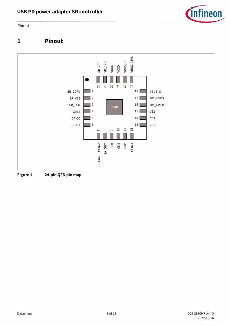
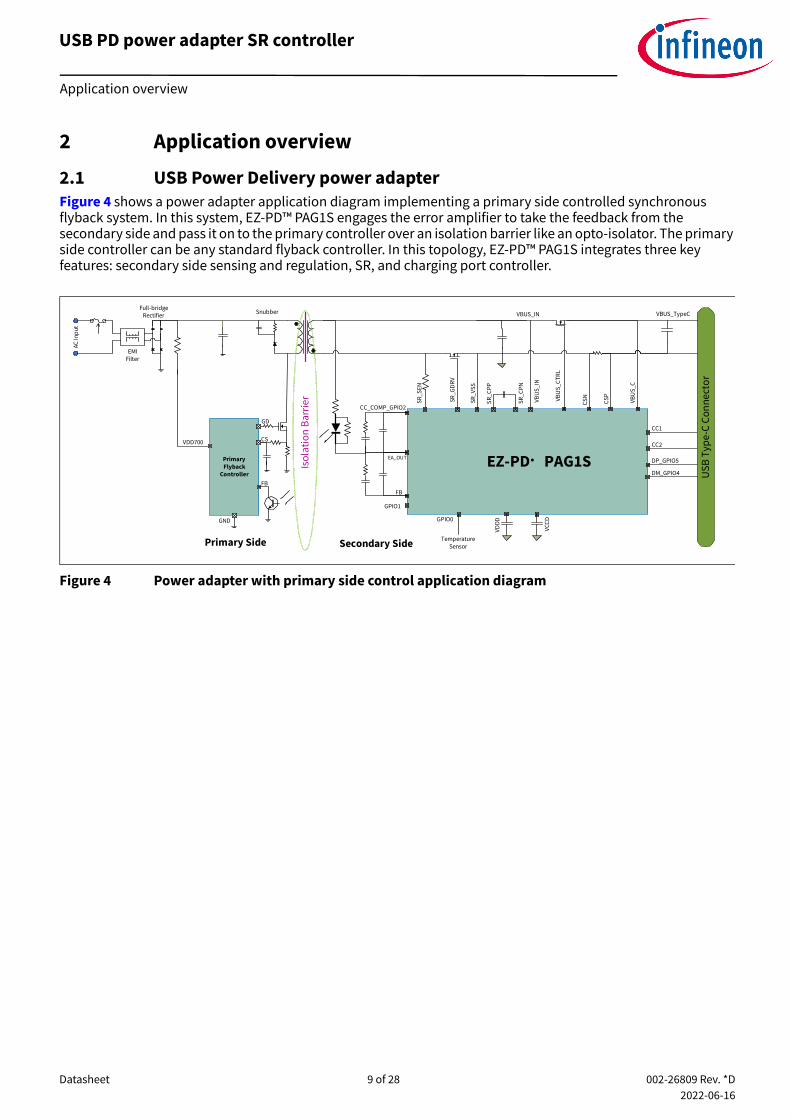
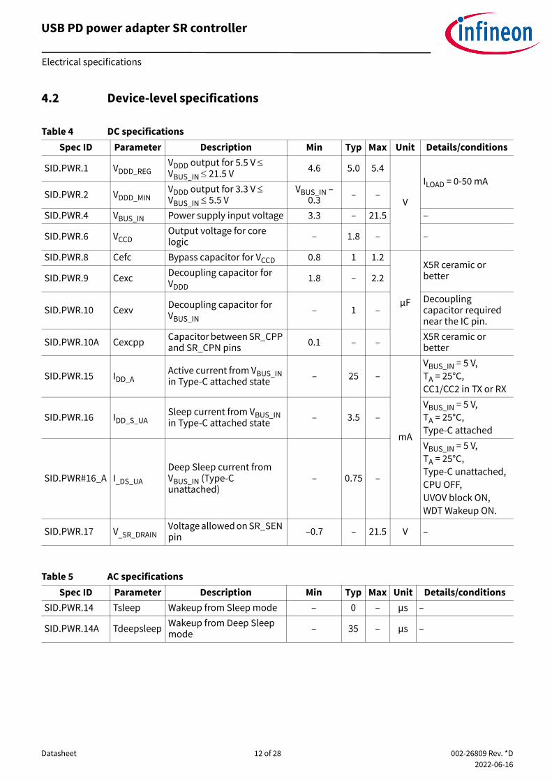
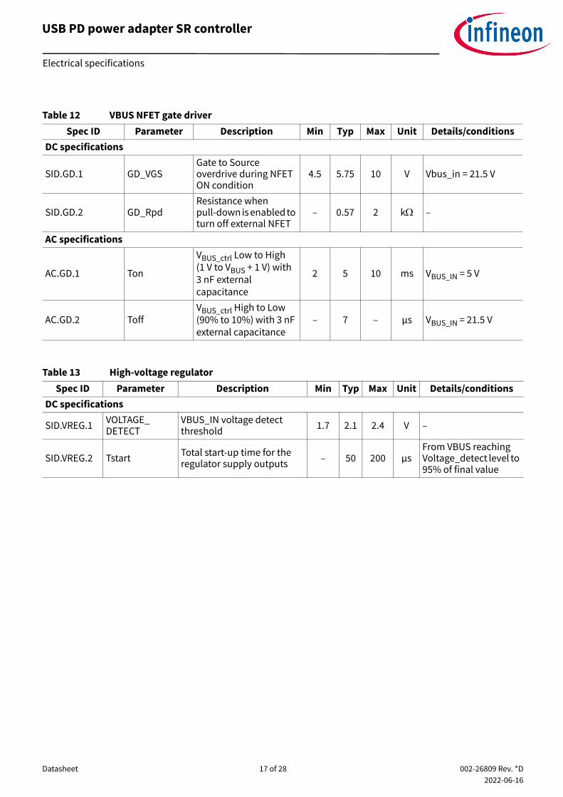
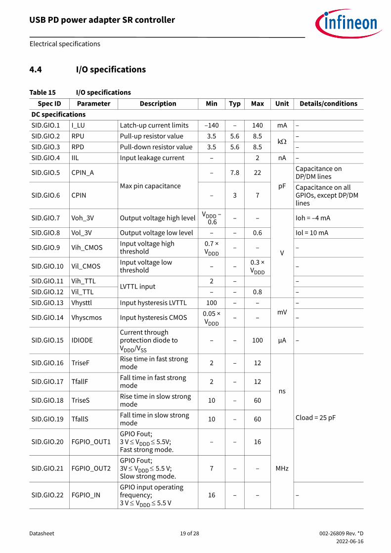
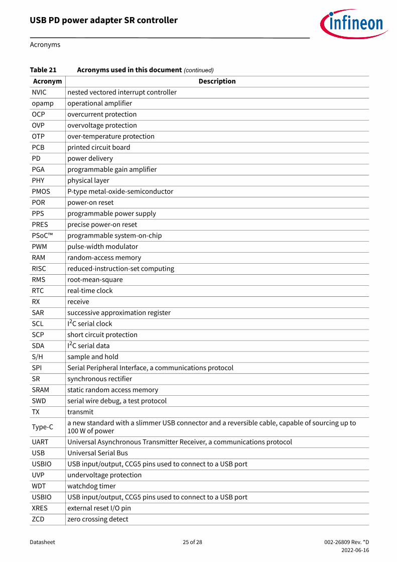
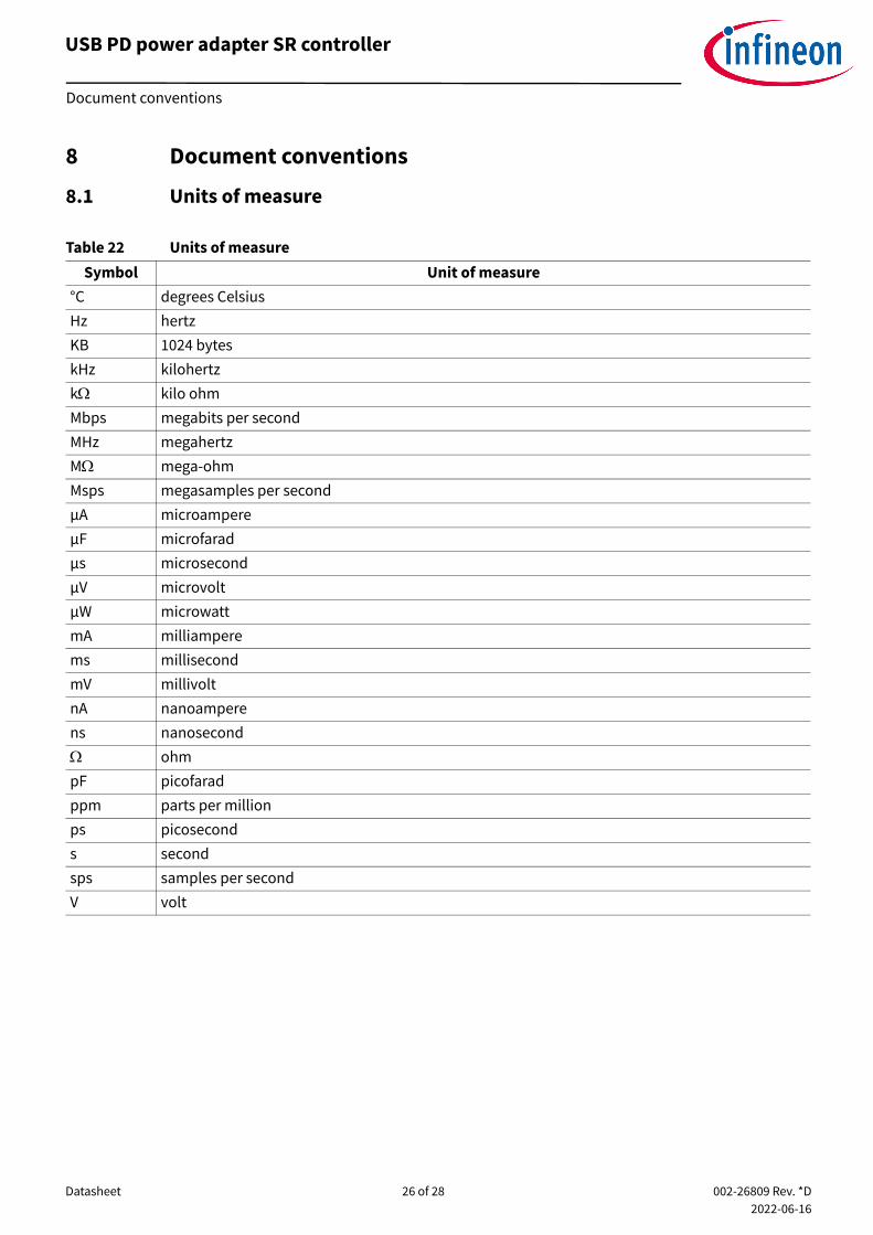