Enabling Content-Centric Device-to-Device Communication in ...
Upload
khangminh22Category
view
0download
0
W81281
USB Keyboard/
Device Controller
查询W81281供应商 捷多邦,专业PCB打样工厂,24小时加急出货

W81281
Publication Release Date: July 1999 - I - Revision 0.60
W81281 Data Sheet Revision History
Pages Dates Version Version
on Web
Main Contents
1 09/01/1997 0.50 First published.
2 All 12/16/1997
7/12/1999
0.51
0.6
Update Features
Update registers description
3
4
5
6
7
8
9
10
11
Please note that all data and specifications are subject to change without notice. All the trade marks of products and companies mentioned in this data sheet belong to their respective owners.
LIFE SUPPORT APPLICATIONS These products are not designed for use in life support appliances, devices, or systems where malfunction of these products can reasonably be expected to result in personal injury. Winbond customers using or selling these products for use in such applications do so at their own risk and agree to fully indemnify Winbond for any damages resulting from such improper use or sales.

W81281
Preliminary
Publication Release Date: July 1999 Revision 0.60
II
TABLE OF CONTENT
1. GENERAL DESCRIPTION ................................................................................................................1
2. FEATURES .........................................................................................................................................2
3 BLOCK DIAGRAM .............................................................................................................................3
4. PIN CONFIGURATION ......................................................................................................................4
5. PIN DESCRIPTION ............................................................................................................................6
5.1 40 PIN DIP...........................................................................................................................................6 5.2 28-PIN SOP .........................................................................................................................................8 5.3 48-PIN LQFP ......................................................................................................................................9
6 FUNCTIONAL DESCRIPTION ...............................................................................................................11
6.1 FIRST IN FIRST OUT STORAGE (FIFO'S) ORGANIZATION ....................................................................11 6.1.1 INTERFACE TO THE MICROCONTROLLER:.......................................................................11
6.2 REGISTER DESCRITPION ......................................................................................................................12 6.2.1 Status Registers ........................................................................................................................12 6.2.2 Control Registers .......................................................................................................................13
6.3 RESET .................................................................................................................................................15 6.3.1 External Reset (Hardware Reset) ............................................................................................16 6.3.2 Warm Reset (Software Reset) .................................................................................................16
6.4 USB SUSPEND.................................................................................................................................16 6.5 USB RESUME:..................................................................................................................................16
7. PROGRAMMING NOTES: ..............................................................................................................17
7.1 CONTROL REGISTERS ACCESS: ...........................................................................................................17 7.2 STATUS REGISTERS ACCESS:..............................................................................................................17 7.3 FIFOS ACCESS : .................................................................................................................................17 7.4 SET STALL FOR ENDPOINT 0 - 4 : ........................................................................................................17 7.5 SET NULL DATA FOR IN TRANSACTION OF EP 0 :................................................................................18
8. ELECTRICAL CHARACTERISTICS & CAPACITANCE ..............................................................19
9. USB KEYBOARD SAMPLE APPLICATION .................................................................................22
10. PACKAGE DIMENSIONS................................................................................................................24
APPENDIX A: WINBOND( W81281-004) DEFAULT MATRIX CODE .................................................28

W81281
USB Keyboard/ Device Controller
Publication Release Date: July 1999 - 1 - Revision 0.60
1. GENERAL DESCRIPTION
W81281 is a low cost, high integration single-chip microcontroller with Universal Serial Bus (USB) interface for keyboard application, it includes the core of Winbond 8-bit microprocessor W78C52 which works on 6MHz. It implements a standard PC keyboard and enables connection to host system through low-speed (1.5Mhz) USB connection . It complies with USB Specification Revision 1.0 and HID Class Definition Revision 1.0.
For Keyboard application, W81281 supports an 18 X 8 keyboard scan matrix, which allows suspend wake up, and also provides a port for PS/2 mouse. It consists of an 8051 compatible CPU core, a 6K-byte ROM, a 256-byte SRAM, and three 16-bit programmable timers.
W81281 supports one device address and five endpoints, one bi-directional endpoint for Control transfer and four unidirectional endpoints for Interrupt IN transfer. Through modification of firmware of W78C52, it can be used for multifunction device design, such as USB-IR receiver and any Slow-Speed (1.5Mhz) USB peripheral device controller.

W81281
Preliminary
Publication Release Date: July 1999 Revision 0.60
2
2. FEATURES Fully compliant with USB spec. Rev.1.0 and HID Class Rev. 1.0
Supporting one device address and five endpoints (one Control transfer, four Interrupt transfer)
Implementing USB keyboard with PS/2 mouse connection
Microsoft Intellimouse(3D mouse) Supported
Supporting 8-bit sense (row) input with wake up interrupt on falling edge, internal pull-ups
Supporting 18-bit drive (column) output, open drain with pull-ups
8-bit 8051 compatible CPU core
6K-byte ROM
256-byte SRAM
3 direct drive LED outputs with internal series resisters
Supporting warm reset
Built-in low voltage reset and EFT/ESD protection circuit
Built-in Watch-Dog Timer for device recovery
Support Win98 system control function
Support suspend/wake-up function, suspend current under 500µA
Internal 3.3V regulator supported
40-pin DIP, 28-pin SOP and 48-pin LQFP packages
5V CMOS Device

Preliminary
Publication Release Date: 1999 60
3 Winbond USB Keyboard/HID Controller
Winbond USB Keyboard/HID Controller
(W81281)
8052
Micro
Processor
Clock
Generator
USB
TransceiverUSB SIE
Endpoints
INT
5V to 3.3V
Conversion
External Clock Circuit
VSS
VBUS
.
.
.
P02SO*
P1SI*
RST
VDD
(x18)
(x8)
PSCL PSDA
LED0-2(P33-P35)
(x3)
(P32) (P31)
*P02SO: P00-P07,P20-P27,SCO16,SCO17
*P1SI:P10-P17
D+
D-
X1 X2
XFRI
Watch Dog
Timer
Power Down
Control
EFT, LVRST
IDSEL(P30)

W81281
Preliminary
Publication Release Date: July 1999 Revision 0.60
4
4. PIN CONFIGURATION
1
2
3
4
5
6
7
8
9
10
11
12
13
14
15
16
17
18
19
20
VSSD+
D-
VDD3
SI0/P10
SO04/P04
SO07/P07
IDSEL/P30
LED0/P33
PSCLK/P32
PSDA/P31LED1/P34
LED2/P35
RESET
X2
SO17
SO16
SO00/P00
SI7/P17
SO09/P21
SO08/P20
VDDX1
40
3938
37
36
35
34
33
32
31
30
29
28
27
26
25
24
23
2221
SO015/P27
SO010/P22
SO011/P23SO012/P24
SO013/P25SO014/P26
SI6/P16
SI5/P15
SI4/P14
SO01/P01
SO02/P02
SO03/P03SI1/P11
SI2/P12SI3/P13
SO05/P05
SO06/P06
40-PIN DIP
1
2
3
4
5
6
7
8
9
10 11
12
13
14
VSS VSS
D+ D -
VDD3 AD04
AD05
AD06
AD07
XALE XWR
XRD
RESET
X2 15
16 17 18 19
20
AD00
AD01
AD02
AD03
WK0
WK1
WK2
WK3
NC
NC XMODE
XINT
VDD
X1
28
27
26
25
24
23
22 21
28-PIN SOP

W81281
Preliminary
Publication Release Date: July 1999 Revision 0.60
5
1 12
13
242536
37
48
VD
D3
SI0
/P1
0
SI1
/P1
1
SI2
/P1
2
SI3
/P1
3
NC
SO
04
/P0
4
SO
05
/P0
5
SO
06
/P0
6
SO
07
/P0
7
IDS
EL
/P3
0
NC
LED0/P33
PSCLK/P32
PSDA/P31
NC
SO09/P21
SO08/P20
VDD
X1
X2
RESET
LED2/P35
LED1/P34
SO
10
/P2
2
SO
11
/P2
3
SO
12
/P2
4
SO
13
/P2
5
SO
14
/P2
6
SO
15
/P2
7
SI7
/P1
7
SI6
/P1
6
SI5
/P1
5
SI4
/P1
4
SO
03
/P0
3
SO
02
/P0
2
SO01/P02
SO00/P00
SO16
SO17
EESCL
VID1
VID0
EESDA
VSS
D+
D-
VSS
W81281D
48-pin LQFP

W81281
Preliminary
Publication Release Date: July 1999 Revision 0.60
6
5. PIN DESCRIPTION
5.1 40 PIN DIP
PIN NO. NAME TYPE DESCRIPTION 1 VSS POWER Ground
2 D+ I/O USB signal (+)
3 D- I/O USB signal (-)
4 VDD3 POWER DC power 3.3V output
5 SI0/P10 I/O Keyboard scan Input 0 / Internal µC IO port 1.0
6 SI1/P11 I/O Keyboard scan Input 1 / Internal µC IO port 1.1
7 SI2/P12 I/O Keyboard scan Input 2 / Internal µC IO port 1.2
8 SI3/P13 I/O Keyboard scan Input 3 / Internal µC IO port 1.3
9 SO04/P04 I/O Keyboard scan Output 04 / Internal µC IO port 0.4
10 SO05/P05 I/O Keyboard scan Output 05 / Internal µC IO port 0.5
11 SO06/P06 I/O Keyboard scan Output 06 / Internal µC IO port 0.6
12 SO07/P07 I/O Keyboard scan Output 07 / Internal µC IO port 0.7
13 IDSEL/P30 I/O Vendor ID selection / Internal µC IO port 3.0
14 LED0/P33 I/O Num. Lock LED / Internal µC IO port 3.3
15 PSCLK/P32 I/O PS/2 mouse clock pin / Internal µC IO port 3.2
16 PSDA/P31 I/O PS/2 mouse data pin / Internal µC IO port 3.1
17 LED1/P34 I/O Caps Lock LED / Internal µC IO port 3.4
18 LED2/P35 I/O Scroll Lock LED / Internal µC IO port 3.5
19 RESET INPUT Chip reset pin
20 X2 OUTPUT Clock output
21 X1 INPUT Clock input
22 VDD POWER VDD power
23 SO08/P20 I/O Keyboard scan Output 08 / Internal µC IO port 2.0
24 SO09/P21 I/O Keyboard scan Output 09 / Internal µC IO port 2.1
25 SO10/P22 I/O Keyboard scan Output 10 / Internal µC IO port 2.2
26 SO11/P23 I/O Keyboard scan Output 11 / Internal µC IO port 2.3
27 SO12/P24 I/O Keyboard scan Output 12 / Internal µC IO port 2.4
28 SO13/P25 I/O Keyboard scan Output 13 / Internal µC IO port 2.5

W81281
Preliminary
Publication Release Date: July 1999 Revision 0.60
7
5.1 40-PIN DIP, continued
PIN NO. NAME TYPE DESCRIPTION 29 SO14/P26 I/O Keyboard scan Output 14 / Internal µC IO port 2.6
30 SO15/P27 I/O Keyboard scan Output 15 / Internal µC IO port 2.7
31 SI7/P17 I/O Keyboard scan Input 7 / Internal µC IO port 1.7
32 SI6/P16 I/O Keyboard scan Input 6 / Internal µC IO port 1.6
33 SI5/P15 I/O Keyboard scan Input 5 / Internal µC IO port 1.5
34 SI4/P14 I/O Keyboard scan Input 4 / Internal µC IO port 1.4
35 SO03/P03 I/O Keyboard scan Output 03 / Internal µC IO port 0.3
36 SO02/P02 I/O Keyboard scan Output 02 / Internal µC IO port 0.2
37 SO01/P01 I/O Keyboard scan Output 01 / Internal µC IO port 0.1
38 SO00/P00 I/O Keyboard scan Output 00 / Internal µC IO port 0.0
39 SO16 OUTPUT Keyboard scan Output 16
40 SO17 OUTPUT Keyboard scan Output 17

W81281
Preliminary
Publication Release Date: July 1999 Revision 0.60
8
5.2 28-PIN SOP
PIN NO. NAME TYPE DESCRIPTION 1 VSS POWER Ground
2 VSS POWER Ground
3 D+ I/O USB signal (+)
4 D- I/O USB signal (-)
5 VDD3 POWER DC power 3.3V output
6 AD04 I/O µC Interface AD04 (Address/Data 04)
7 AD05 I/O µC Interface AD05 (Address/Data 05)
8 AD06 I/O µC Interface AD06 (Address/Data 06)
9 AD07 I/O µC Interface AD07 (Address/Data 07)
10 XALE I/O µC Interface ALE (Address Latch Enable)
11 XWR I/O µC Interface WR (Data Write)
12 XRD I/O µC Interface RD (Data Read)
13 RESET INPUT Chip reset pin
14 X2 OUTPUT Clock output
15 X1 INPUT Clock input
16 VDD POWER VDD power
17 XINT I/O µC Interface INT (Interrupt)
18 XMODE I/O Controller mode setting, it should be kept high
19 NC I/O Not Used
20 NC I/O Not Used
21 WK3 INPUT Wakeup pin, Active low and keep more than 100ns
22 WK2 INPUT Wakeup pin, Active low and keep more than 100ns
23 WK1 INPUT Wakeup pin, Active low and keep more than 100ns
24 WK0 INPUT Wakeup pin, Active low and keep more than 100ns
25 AD03 I/O µC Interface AD03 (Address/Data 03)
26 AD02 I/O µC Interface AD02 (Address/Data 02)
27 AD01 I/O µC Interface AD01 (Address/Data 01)
28 AD00 I/O µC Interface AD00 (Address/Data 00)

W81281
Preliminary
Publication Release Date: July 1999 Revision 0.60
9
5.3 48-PIN LQFP
PIN NO. NAME TYPE DESCRIPTION 1 VDD3 POWER DC power 3.3V output
2 SI0/P10 I/O Keyboard scan Input 0 / Internal µC IO port 1.0
3 SI1/P11 I/O Keyboard scan Input 1 / Internal µC IO port 1.1
4 SI2/P12 I/O Keyboard scan Input 2 / Internal µC IO port 1.2
5 SI3/P13 I/O Keyboard scan Input 3 / Internal µC IO port 1.3
6 NC none Not Used
7 SO04/P04 I/O Keyboard scan Output 04 / Internal µC IO port 0.4
8 SO05/P05 I/O Keyboard scan Output 05 / Internal µC IO port 0.5
9 SO06/P06 I/O Keyboard scan Output 06 / Internal µC IO port 0.6
10 SO07/P07 I/O Keyboard scan Output 07 / Internal µC IO port 0.7
11 IDSEL/P30 I/O Vendor ID selection / Internal µC IO port 3.0
12 NC none Not Used
13 LED0/P33 I/O Num. Lock LED / Internal µC IO port 3.3
14 PSCLK/P32 I/O PS/2 mouse clock pin / Internal µC IO port 3.2
15 PSDA/P31 I/O PS/2 mouse data pin / Internal µC IO port 3.1
16 LED1/P34 I/O Caps Lock LED / Internal µC IO port 3.4
17 LED2/P35 I/O Scroll Lock LED / Internal µC IO port 3.5
18 RESET INPUT Chip reset pin
19 X2 OUTPUT Clock output
20 X1 INPUT Clock input
21 VDD POWER VDD power
22 SO08/P20 I/O Keyboard scan Output 08 / Internal µC IO port 2.0
23 SO09/P21 I/O Keyboard scan Output 09 / Internal µC IO port 2.1
24 NC none Not Used
25 SO10/P22 I/O Keyboard scan Output 10 / Internal µC IO port 2.2
26 SO11/P23 I/O Keyboard scan Output 11 / Internal µC IO port 2.3
27 SO12/P24 I/O Keyboard scan Output 12 / Internal µC IO port 2.4
28 SO13/P25 I/O Keyboard scan Output 13 / Internal µC IO port 2.5
29 SO14/P26 I/O Keyboard scan Output 14 / Internal µC IO port 2.6
30 SO15/P27 I/O Keyboard scan Output 15 / Internal µC IO port 2.7

W81281
Preliminary
Publication Release Date: July 1999 Revision 0.60
10
5.3 48-PIN LQFP, continued
PIN NO. NAME TYPE DESCRIPTION 31 SI7/P17 I/O Keyboard scan Input 7 / Internal µC IO port 1.7
32 SI6/P16 I/O Keyboard scan Input 6 / Internal µC IO port 1.6
33 SI5/P15 I/O Keyboard scan Input 5 / Internal µC IO port 1.5
34 SI4/P14 I/O Keyboard scan Input 4 / Internal µC IO port 1.4
35 SO03/P03 I/O Keyboard scan Output 03 / Internal µC IO port 0.3
36 SO02/P02 I/O Keyboard scan Output 02 / Internal µC IO port 0.2
37 SO01/P01 I/O Keyboard scan Output 01 / Internal µC IO port 0.1
38 SO00/P00 I/O Keyboard scan Output 00 / Internal µC IO port 0.0
39 SO16 OUTPUT Keyboard scan Output 16
40 SO17 OUTPUT Keyboard scan Output 17
41 EESCL OUTPUT Clock pin of External serial EEPROM
42 VID1 INPUT Vendor ID selection 1
43 VID0 INPUT Vendor ID selection 0
44 EESDA I/O Data pin of External serial EEPROM
45 VSS POWER Ground
46 VSS POWER Ground
47 D+ I/O USB signal (+)
48 D- I/O USB signal (-)

W81281
Preliminary
Publication Release Date: July 1999 Revision 0.60
11
6 FUNCTIONAL DESCRIPTION
6.1 First In First Out Storage (FIFO'S) Organization
The W81281 has six FIFO's, one for receiving and five for transmitting.
FIFO or SRAM
SIZE (Byte ) NOTES
Endpt 0 Receiving
8 Data received on upstream port which contains the correct address and pids will be stored here for the CPU core to read.
Endpt 0 Transmitting
8 The CPU core writes the data here which will be sent to the host when the correct address and pids are transmitted by the host.
Endpt 1 Transmitting
8 The CPU core writes the data here which will be sent to the host when the correct address and pids are transmitted by the host.
Endpt 2 Transmitting
8 The CPU core writes the data here which will be sent to the host when the correct address and pids are transmitted by the host.
Endpt 3 Transmitting
8 The CPU core writes the data here which will be sent to the host when the correct address and pids are transmitted by the host.
Endpt 4 Transmitting
8 The CPU core writes the data here which will be sent to the host when the correct address and pids are transmitted by the host.
6.1.1 INTERFACE TO THE MICROCONTROLLER:
The FIFOs communicate with the CPU core by address 06H 0f External DATA Memory Access of CPU during IP.6 = "1".The FIFO access steps are firstly set IP.6 = "1" in CPU core. Secondly, CPU core selects FIFO to access by setting the followed bits in control register 2 :
EP0_RD_EN : read "IN" FIFO of Endpoint 0 ( EP0 ).
EP0_WR_EN : write "OUT" FIFO of Endpoint 0 ( EP0 ).
EP1_WR_EN : write "OUT" FIFO of Endpoint 1 ( EP1 ).
EP2_WR_EN : write "OUT" FIFO of Endpoint 2 ( EP2 ).
EP3_WR_EN : write "OUT" FIFO of Endpoint 3 ( EP3 ).
EP4_WR_EN : write "OUT" FIFO of Endpoint 4 ( EP4 ).
Then access FIFO by address 06H of External DATA Memory Access of CPU. For detailed programming steps, refer to section 7.3 Programming Note.

W81281
Preliminary
Publication Release Date: July 1999 Revision 0.60
12
6.2 Register Descritpion
The CPU core accesses registers by External DATA Memory Access during IP.6 = "1"‘1’
6.2.1 Status Registers
CPU core can set "High" at USB_EventINT_EN bit of control register 4 to enable interrupt of USB events to INT0. When interrupt comes, CPU reads status register 0 and 1 to check which event occurs. ( refer to section 7.2 for accessing Status Registers )
Status Register 0: Address = 00H (Interrupt Event Flags)
BIT SYMBOL DESCRIPTION
7 NAK_EP0_IN NAK occurs from EP0 for IN Transaction. ( only valid during NakEP0In_INT_EN = 1 in Control Register 3 )
6 ACK_EP0_SETUP ACK occurs from EP0 for SETUP Transaction
5 ACK_EP0_OUT ACK occurs from EP0 for OUT Transaction
4 ACK_EP0_IN ACK occurs from EP0 for IN Transaction
3 ACK_EP1_IN ACK occurs from EP1 for IN Transaction
2 ACK_EP2_IN ACK occurs from EP2 for IN Transaction
1 ACK_EP3_IN ACK occurs from EP3 for IN Transaction
0 ACK_EP4_IN ACK occurs from EP4 for IN Transaction
Status Register 1: Address = 01H (Interrupt Event Flags)
BIT SYMBOL DESCRIPTION
7-6 VID[1:0] Keyboard Scan Matrix Selection.
5 Reserved must ignore this value.
4 EP0OutNullData receiving Null Data at EP0 during OUT Transaction
3 Suspend_In Suspend Mode active ( no traffic on USB Bus > 3 mS )
2 USB_Reset receiving Reset command from USB Bus
1 Resume_In receiving Resume command from USB Bus
0 Reserved must ignore this value

W81281
Preliminary
Publication Release Date: July 1999 Revision 0.60
13
Status Register 2: Address = 07H (Data Byte Count of EP0 IN FIFO)
BIT SYMBOL DESCRIPTION
7-4 Reserved must ignore those values
3-0 DataLength_CNT[3:0] Number of Data byte for EP0 FIFO ( receiving Data from USB Bus )
6.2.2 Control Registers
( All registers are set to 00h at power up.)( refer to section 7.1 for accessing Control Registers )
Control Register 0: Address = 02H (Endpoint Enable Control)
BIT SYMBOL DESCRIPTION
7-5 Reserved must keep bits = “0”
4 USB_Speed set igh” for Full Speed; set "Low" for Low Speed
3 EP1_EN set "High" to enable Endpoint 1
2 EP2_EN set "High" to enable Endpoint 2
1 EP3_EN set "High" to enable Endpoint 3
0 EP4_EN set "High" to enable Endpoint 4
Control Register 1: Address = 03H (Device Address Setting)
BIT SYMBOL DESCRIPTION
7 Bus_Connection connect up stream port on USB Bus after chip initialization done
6-0 Device_Address[6:0] Setup Device Address
Control Register 2: Address = 04H (FIFO Access Control)
BIT SYMBOL DESCRIPTION
7 Reserved must keep bit = "0".
6 Set_Stall Set Stall for EP 0 -4 ( refer to section 7.4 for programming )

W81281
Preliminary
Publication Release Date: July 1999 Revision 0.60
14
5 EP0_RD_EN Set "High" before reading IN FIFO of EP0 (receiving Data from USB Bus )
4 EP0_WR_EN Set "High" before writting OUT FIFO of EP0 (transmitting Data to USB Bus )
3 EP1_WR_EN Set "High" before writting OUT FIFO of EP1 (transmitting Data to USB Bus )
2 EP2_WR_EN Set "High" before writting OUT FIFO of EP2 (transmitting Data to USB Bus )
1 EP3_WR_EN Set "High" before writting OUT FIFO of EP3 (transmitting Data to USB Bus )
0 EP4_WR_EN Set "High" before writting OUT FIFO of EP4 (transmitting Data to USB Bus )
Control Register 3: Address = 05H (USB Event Control)
BIT SYMBOL DESCRIPTION
7 Reserved must keep bit = "0"
6 NakEP0In_INT_EN Enable interrupt event when NAK comes from EP0 for IN Transaction
5 Set_EP0NullData set Null Data for IN Transaction of EP 0 ( refer to section 7.5 for programming )
4 Warm_Reset Active Warm Reset
3 Resume_Out Send Resume command (K-state) to USB Bus ( Set_Suspend should be “1” )
2 Set_Suspend Set suspend mode active
1 Read_Event Set "High" during reading Status Registers ( refer to section 7.2 for programming )
0 Set_EP0_Nak Set "High" for responsing Nak when IN/OUT Transaction of EP0 come

W81281
Preliminary
Publication Release Date: July 1999 Revision 0.60
15
Control Register 4: Address = 08H (Interrupt Enable Control)
BIT SYMBOL DESCRIPTION
7-4 Reserved must keep bits = "0"
3 Remote_Wakeup_EN for Remote Wakeup Enable from Keystroke or Mouse moving
2 USB_EventINT_EN for USB event interrupt enable
1 SCANOUT[17] output port value of port SO17
0 SCANOUT[16] output port value of port SO16
Control Register 5: Address = 09H (CPU Reset Control)
BIT SYMBOL DESCRIPTION
7-2 Reserved must keep bit = "0"
1 UC_WarmReset_EN set "High" for reseting CPU when Warm_Reset = "1"
0 DisconUSB_Bus_Disable set "High" keeping device conecting with USB Bus during software or hardware reset
set ow” disconnecting with USB Bus during software or
hardware reset
Control Register 6: Address = 0EH (Watch Dog Timer Reset)
BIT SYMBOL DESCRIPTION
7-0 Reset_WDT Clear WDT = 00H when set Reset_WDT = AAH
6.3 Reset
The W81281 supports three types of reset. During a reset, all registers of the CPU core and USB return to their default status, and USB device address is set to zero.

W81281
Preliminary
Publication Release Date: July 1999 Revision 0.60
16
6.3.1 External Reset (Hardware Reset)
As in 8051 series controller, the external RESET signal is sampled at S5P2. To take effect, it must be held high at least two machine cycles while the oscillator is running.
An internal trigger circuit in the reset line is used to deglitch the reset line. The reset logic also has a special glitch remocal circuit that ignores glitches on the reset line.
During reset, the ports are initialized to FFH, the stack pointer to 07H, PCON(with exception of bit 4) to 00H, and all of the other SFR registers except SBUF to 00H. SBUF is not reset.
6.3.2 Warm Reset (Software Reset)
W81281 provides a warm reset by setting "High" at Warm_Reset bit of control register 3.
The W81281 handles the USB reset function independently from the CPU core. If a Single Ended Zero (SE0) is detected on the upstream port for greater then 2.5us, then the interrupt is enabled. The CPU core read flag from USB_Reset bit of status register 1 then CPU
- to reset the device address to 0, and enter the default state. No any reset timing occurs.
or
- to set "High" at Warm_Reset bit of control register
6.3.3 WDT Reset (Hardware Reset) There is a Watch Dog Timer installed in W81C281. CPU should periodically clear WDT to 00H by setting Reset_WDT=AAH before WDT time out. If CPU hangs WDT will time-out and cause hardware reset.
6.4 USB SUSPEND
If there is no upstream activity for 3 msec then the Suspend_In flag is set and the interrupt enabled. When Suspend_In flag is read, CPU core actives power down mode for W81281 go into suspend
6.5 USB RESUME:
The suspend state can be exit by a 'resume'. The resume can occur by three methods.
• The host can send a resume to all ports by placing a 0 (K state) on the bus. The W81281 sees the resume, , and enables the interrupt. In this case, the CPU core does not have to perform any functions.
• The host can reset the bus.
• When any falling edge is detected on CPU port1(keystrokes). The CPU core will exit from power down mode and initiate a resume by setting Resume_Out in the Control Register 3 which will cause a K state to be sent. To un-resume, the CPU core must clear the Resume_Out bit in the Control Register 3.

W81281
Preliminary
Publication Release Date: July 1999 Revision 0.60
17
7. PROGRAMMING NOTES: The W81281 uses reserved bit of the Interrupt Priority Register IP.6 as a pre-decoding bit to implement a alternative register and FIFO by External Data Memory Access of CPU core. Programming functions described as below:
7.1 Control Registers Access:
Step 1: set IP.6 = 1
Step 2: access Control Register (by MOVX Instruction)
Step 3: set IP.6 = 0
7.2 Status Registers Access:
Step 1: set IP.6 = 1
Step 2 : set Read_Event = 1 in Control Register 3 ( by MOVX Instruction )
step 3 : access Status Registers ( by MOVX Instruction )
step 4 : set IP.6 = 0
7.3 FIFOs Access :
step 1 : set IP.6 = 1
step 2 : set EP0_RD_EN/EPX_WR_EN = 1 ( X : 0 - 4) (by MOVX Instruction )
step 3 : access FIFO by address 06H of MOVX Instruction
step 4 : set EP0_RD_EN/EPX_WR_EN = 0 ( X : 0 - 4) (by MOVX Instruction )
step 5 : set IP.6 = 0
7.4 Set Stall for Endpoint 0 - 4 :
step 1 : set IP.6 = 1
step 2 : set Set_Stall = 1 (by MOVX Instruction )
step 3 : set EP0_RD_EN/EPX_WR_EN = 1 ( X : 0 - 4) (by MOVX Instruction )
step 4 : set EP0_RD_EN/EPX_WR_EN = 0 ( X : 0 - 4) (by MOVX Instruction )
step 5 : set Set_Stall = 0 (by MOVX Instruction )
step 6 : set IP.6 = 0
Note : 1. EP0_RD_EN = 1 for OUT Transaction of EP0.

W81281
Preliminary
Publication Release Date: July 1999 Revision 0.60
18
2. EP0_WR_EN = 1 for IN Transaction of EP0.
7.5 Set Null Data for IN Transaction of EP 0 :
step 1 : set IP.6 = 1
step 2 : set Set_EP0NullData = 1 (by MOVX Instruction )
step 3 : set EP0_WR_EN = 1 (by MOVX Instruction )
step 4 : set EP0_WR_EN = 0 (by MOVX Instruction )
step 5 : set Set_EP0NullData = 0 (by MOVX Instruction )
step 6 : set IP.6 = 0

W81281
Preliminary
Publication Release Date: July 1999 Revision 0.60
19
8. ELECTRICAL CHARACTERISTICS & CAPACITANCE (Ta = 0¢ Jto + 70¢ J, VDD = +5V ± 5% )
SYMBOL DESCRIPTION MIN. TYP. MAX. UNIT NOTE
VDD Power Support 4.0 5.0 5.5 V
VIL Input Low Voltage (except RESET) 0.8 V
VIL1 Input Low Voltage (RESET) 0.6 V
VIH1 Input High Voltage (except RESET) 2.0 V
VIH2 Input High Voltage (RESET) 3.5 V
VOH Output High Voltage (except D+/D-) 2.4 V IOH=-4mA
VOL Output Low Voltage (except D+/D-) 0.4 V IOL= 4mA
IOFL Output Leakage Current (High-Z state)
-10 10 uA
IIH Input Leakage Current -10 10 uA VDD=5.5V
VIN=VDD
IIL Input Leakage Current -10 10 uA VDD=5.5V
VIN=VSS

W81281
Preliminary
Publication Release Date: July 1999 Revision 0.60
20
Symbol Conditions Min Max Unit D+/D- Leakage Current: Hi-Z State Data Line Leakage ILO 0 V < VIN < 3.3V -10 +10 µA
D+/D- Input Levels: Differential Input Sensitivity VDI (D+)-(D-) 0.2 V
Differential Common Mode Range VCM Includes VDI range 0.8 2.5 V
Single Endge Receiver Threshold VSE 0.8 2.0 V
D+/D- Output Levels: Static Output Low VOL RL of 1.5kΩ to 3.6V 0.3 V
Static Output High VOH RL of 1.5kΩ to GND 2.8 3.6 V
D+/D- Capacitance: Transceiver Capacitance CIN Pin to GND 20 pF
D+/D- Driver Characteristics: Transition Time:
Rise Time
Fall Time
TR
TF
CL=50pF/350pF
CL=50pF/350pF
75
75
300
300
ns
ns
Rise / Fall Time Matching TRFM (TR / TF) 80 125 %
Output Signal Crossover Voltage VCRS 1.3 2.0 V
D+/D- Data Source Timings: Low Speed Data Rate TDRATE Ave.Bit Rate
(1.5Mb/s ±1.5%)
1.4775 1.5225 Mbs
Source Differential Driver Jitter
To Next Transition
For Paired Transitions
TDJ1
TDJ2
-95
-150
95
150
ns
ns
Source EOP Width TEOPT 1.25 1.50 µs
Differential to EOP Transition Skew TDEOP -40 100 ns
D+/D- Data Receiver Timings: Receiver Data Jitter Tolerance
To Next Transition
For Paired Transitions
TDJR1
TDJR2
-75
-45
75
45
ns
ns
Receiver SE0 Tolerance during Differential Transition
TLST 210 ns

W81281
Preliminary
Publication Release Date: July 1999 Revision 0.60
21
EOP Width at receiver
Must reject as EOP
Must accept as EOP
TEORP1
TEOPR2
330
675
ns
ns

W81281
Preliminary
Publication Release Date: July 1999 Revision 0.60
22
9. USB KEYBOARD SAMPLE APPLICATION 1. For 40 pin DIP package
VCC
VCC
VCC
VCC
VCC
VCC
W81281 USB Keyboard ReferenceS h i
or all
Jumper
R 100ohman
not used
be short
Only one
can beshort
whileJ
RESET
X1X2
IDSEL
LED0LED1LED2
PSDA
PSCLK
PSDAPSCLK
X1
RESET
X2
IDSEL
LED2
LED0
LED1
C1
47p
C2
30p
C3
30p
C40.1u
C510u
+
X16MHZ Crystal / Resonator
L1 FBL2 FB
L3
FB
L4
FB
L5
FB
U1
W81281
SI05
SI16
SI27
SI38
SI434
SI533
SI632
SI731
SO038
SO137
SO236
SO335
SO49
SO510
SO611
SO712
SO823
SO924
SO1025
SO1126
SO1227
SO1328
SO1429
SO1530
SO1639
SO1740
VDD22
VDD34
VSS1
RESET19
X121
X220
LED117
LED218
IDSEL13
LED014
D-3
D+2
PSDA16
PSCLK15
C610u
+
R17.5K
C7
47p
JP4
PS/2 MOUSE
123456
L6
FB
USB1USB-CONN
1234
56
C810u
+
R53.3K
L7 FBL8 FB
R6 30R7 30
JP2
JUMPER
R2100
D1NumLock
D2
CapsLoc
D3
ScrollLoc
R4100
JP1
JUMPER
JP3
JUMPER
R3100
U-U+
ScanIn0ScanIn1ScanIn2ScanIn3ScanIn4ScanIn5ScanIn6ScanIn7
ScanOut1ScanOut2ScanOut3ScanOut4ScanOut5ScanOut6ScanOut7
ScanOut8ScanOut9
ScanOut0
ScanOut10ScanOut11ScanOut12ScanOut13ScanOut14ScanOut15
ScanOut16ScanOut17
D-D+
W81281
Preliminary
Publication Release Date: July 1999 Revision 0.60
23
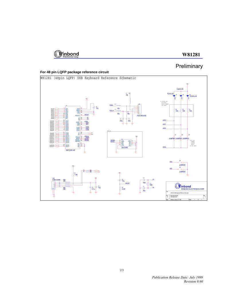
For 48 pin LQFP package reference circuit
281DEMO4.SCH 1.3
W81281 USB Keyboard Reference Schematic
B
1 1Monday, January 25, 1999
Title
Size Document Number Rev
Date: Sheet of
VCC
VCC
VCC
VCC
VCC
VCC
VCC
R 100ohm canbe shortwhile Jumpernot used
Only oneJumpercan beshort
or all open
W81281 (48pin LQFP) USB Keyboard Reference Schematic
Option
PSDA
PSCLK
RESET
X1X2
LED0IDSEL
VID0VID1 LED1
LED0LED1 LED2LED2
PSCLKPSDA
EESCLEESDA EESDA
EESCL
IDSEL
VID0
VID1
X1
RESET
X2
C1
47p
C2
30p
C3
30pWINBOND ELECTRONICS CORP.inbondC4
0.1u
C5
10u+
X1
6ML1
FBL2
FB
L3
FB
L4
FBL5
FB
C6
10u+
R1
7.5K
D1NumLock
D2
CapsLock
D3
ScrollLock
R2
100R3
100R4
100
JP1
JUMPER
JP2
JUMPER
JP3
JUMPER
C7
47p
JP4
PS/2 MOUSE
123456
L6
FB
USB1
USB-CONN
123456
C8
10u+
R5
3.3K
L7
FB
L8
FB
R6 30R7 30
U1
W81C281-48
SI02
SI13
SI24
SI35
SI434
SI533
SI632
SI731
SO038
SO137
SO236
SO335
SO47
SO58
SO69
SO710
SO822
SO923
SO1025
SO1126
SO1227
SO1328
SO1429
SO1530
SO1639
SO1740
VDD21
VDD31
VSS45
X120
LED013
LED116
IDSEL11
D-48
D+47
PSDA15
VSS46
X219
RESET18
LED217
VID043
VID142
PSCLK14
EESDA44EESCL41
NC6
NC12
NC24
U2
24LC04B
A01A12A23VSS4
SDA5
SCL6
RC7
VCC8
JP4
JUMPER
JP5
JUMPERU-U+
ScanIn0ScanIn1ScanIn2ScanIn3ScanIn4ScanIn5ScanIn6ScanIn7
ScanOut1ScanOut2ScanOut3ScanOut4ScanOut5ScanOut6ScanOut7
ScanOut8ScanOut9
ScanOut0
ScanOut10ScanOut11ScanOut12ScanOut13ScanOut14ScanOut15
ScanOut16ScanOut17
D-D+

W81281
Preliminary
Publication Release Date: July 1999 Revision 0.60
24
10. PACKAGE DIMENSIONS 40-pin DIP
1.371.220.0540.048
Notes:
Symbol Min. Nom. Max. Max.Nom.Min.Dimension in inches Dimension in mm
A
B
cD
e
A
L
S
AA
1
2
E
0.050 1.27
0.210 5.33
0.010
0.150
0.016
0.155
0.018
0.160
0.022
3.81
0.41
0.25
3.94
0.46
4.06
0.56
0.008
0.120
0.670
0.010
0.130
0.014
0.140
0.20
3.05
0.25
3.30
0.36
3.56
0.540 0.5500.545 13.72 13.9713.84
17.02
15.2414.99 15.490.6000.590 0.610
2.29 2.54 2.790.090 0.100 0.110
B 1
1
e
E 1
a
2.055 2.070 52.20 52.58
0 15
0.090 2.29
0.6500.630 16.00 16.51
1. Dimensions D Max & S include mold flash ortie bar burrs.
2. Dimension E1 does not include interlead flash.3. Dimensions D & E1 include mold mismatch and
are determined at the mold parting line.
6. General appearance spec. should be based onfinal visual inspection spec.
.
protrusion/intrusion.4. Dimension B1 does not include dambar
5. Controlling dimension: Inches.
150
Seating Plane
e A
2A
a
c
E
Base Plane1A
1e
L
A
S
1E
D
1B
B
40 21
201
28-pin SOP
L
O
c
E H
A1
A
e
b
D
SEATING PLANE
Y
0.25
GAUGE PLANE
E
1
28 15
14
7.60
0.32
0.51
0.30
E
c
b
A1
7.40
0.23
0.33
0.10
0.299
0.013
0.020
0.012
0.291
0.009
0.013
0.004
MAX.
DIMENSION IN MM
2.65A
SYMBOLMIN.
2.35
DIMENSION IN INCH
0.104
MIN.
0.093
MAX.
Control demensions are in milme
1.27
0.10
10.65
L
θ
Y
H
0 8
0.40
10.00
e 1.27 BSC
0.050
0.004
0.419
0
0.016
0.394
8
0.050 BSC
E
D 17.70 18.10 0.697 0.713

W81281
Preliminary
Publication Release Date: July 1999 Revision 0.60
25
48-pin LQFP
2
1A
H
D
D
e b
E H E
y
AA
Seating Plane L
L 1
See Detail F
Detail F
c
37
48
1 12
13
24
2536
1. Dimensions D & E do not include interleadflash.
2. Dimension b does not include dambarprotrusion/intrusion.
3. Controlling dimension: Millimeters4. General appearance spec. should be based
on final visual inspection spec.
Notes:
Symbol Min. Nom. Max. Max.Nom.Min.
Dimension in inch Dimension in mm
A
bcD
eHD
HE
L
y0
AA
L1
1
2
E
1.40
0.20
0.50
1.00
7.00
9.00
9.00
7.00
---
------ 1.60
0.15
1.451.35
0.05
0.17 0.27
---0.09 0.20
0.45 0.60 0.75
0.08
0 3.5 7
--- ---
HeadquartersNo. 4, Creation Rd. IIIScience-Based Industrial ParkHsinchu, TaiwanTEL: 886-35-770066FAX: 886-35-789467www: http://www.winbond.com.tw/
Taipei Office11F, No. 115, Sec. 3, Min-Sheng East Rd.Taipei, TaiwanTEL: 886-2-7190505FAX: 886-2-7197502TLX: 16485 WINTPE
Winbond Electronics (H.K.) Ltd.Rm. 803, World Trade Square, Tower II123 Hoi Bun Rd., Kwun TongKowloon, Hong KongTEL: 852-27516023-7FAX: 852-27552064
Winbond Electronics(North America) Corp.2730 Orchard ParkwaySan Jose, CA 95134 U.S.A.TEL: 1-408-9436666FAX: 1-408-9436668

W81281
Preliminary
Publication Release Date: July 1999 Revision 0.60
26

W81281
Preliminary
Publication Release Date: July 1999 Revision 0.60
27

W81281
Preliminary
Publication Release Date: July 1999 Revision 0.60
28
VCC
VCC
VCC
VCC
VCC
VCC
W81281 USB Keyboard Referenceh i
or allopen
Jumper
R 100ohman
not used
be short
Only one
can beshort
whileJumper
RESET
X1X2
IDSEL
LED0LED1LED2
PSDA
PSCLK
PSDAPSCLK
X1
RESET
X2
IDSEL
LED2
LED0
LED1
C1
47p
C2
30p
C3
30p
C40.1u
C510u
+
X16MHZ Crystal / Resonator
L1 FBL2 FB
L3
FB
L4
FB
L5
FB
U1
W81281
SI05
SI16
SI27
SI38
SI434
SI533
SI632
SI731
SO038
SO137
SO236
SO335
SO49
SO510
SO611
SO712
SO823
SO924
SO1025
SO1126
SO1227
SO1328
SO1429
SO1530
SO1639
SO1740
VDD22
VDD34
VSS1
RESET19
X121
X220
LED117
LED218
IDSEL13
LED014
D-3
D+2
PSDA16
PSCLK15
C610u
+
R17.5K
C7
47p
JP4
PS/2 MOUSE
123456
L6
FB
USB1USB-CONN
1234
56
C810u
+
R53.3K
L7 FBL8 FB
R6 30R7 30
JP2
JUMPER
R2100
D1NumLoc D2
CapsLoc
D3
ScrollLoc
R4100
JP1
JUMPER
JP3
JUMPER
R3100
U-U+
ScanIn0ScanIn1ScanIn2ScanIn3ScanIn4ScanIn5ScanIn6ScanIn7
ScanOut1ScanOut2ScanOut3ScanOut4ScanOut5ScanOut6ScanOut7
ScanOut8ScanOut9
ScanOut0
ScanOut10ScanOut11ScanOut12ScanOut13ScanOut14ScanOut15
ScanOut16ScanOut17
D-D+
281DEMO4.SCH 1.3
W81281 USB Keyboard Reference Schematic
B
1 1Monday, January 25, 1999
Title
Size Document Number Rev
Date: Sheet of
VCC
VCC
VCC
VCC
VCC
VCC
VCC
R 100ohm canbe shortwhile Jumpernot used
Only oneJumpercan beshort
or all open
W81281 (48pin LQFP) USB Keyboard Reference Schematic
Option
PSDA
PSCLK
RESET
X1X2
LED0IDSEL
VID0VID1 LED1
LED0LED1 LED2LED2
PSCLKPSDA
EESCLEESDA EESDA
EESCL
IDSEL
VID0
VID1
X1
RESET
X2
C1
47p
C2
30p
C3
30pWINBOND ELECTRONICS CORP.inbondC4
0.1u
C5
10u+
X1
6ML1
FBL2
FB
L3
FB
L4
FBL5
FB
C6
10u+
R1
7.5K
D1NumLock
D2
CapsLock
D3
ScrollLock
R2
100R3
100R4
100
JP1
JUMPER
JP2
JUMPER
JP3
JUMPER
C7
47p
JP4
PS/2 MOUSE
123456
L6
FB
USB1
USB-CONN
123456
C8
10u+
R5
3.3K
L7
FB
L8
FB
R6 30R7 30
U1
W81C281-48
SI02
SI13
SI24
SI35
SI434
SI533
SI632
SI731
SO038
SO137
SO236
SO335
SO47
SO58
SO69
SO710
SO822
SO923
SO1025
SO1126
SO1227
SO1328
SO1429
SO1530
SO1639
SO1740
VDD21
VDD31
VSS45
X120
LED013
LED116
IDSEL11
D-48
D+47
PSDA15
VSS46
X219
RESET18
LED217
VID043
VID142
PSCLK14
EESDA44EESCL41
NC6
NC12
NC24
U2
24LC04B
A01A12A23VSS4
SDA5
SCL6
RC7
VCC8
JP4
JUMPER
JP5
JUMPERU-U+
ScanIn0ScanIn1ScanIn2ScanIn3ScanIn4ScanIn5ScanIn6ScanIn7
ScanOut1ScanOut2ScanOut3ScanOut4ScanOut5ScanOut6ScanOut7
ScanOut8ScanOut9
ScanOut0
ScanOut10ScanOut11ScanOut12ScanOut13ScanOut14ScanOut15
ScanOut16ScanOut17
D-D+
APPENDIX A: WINBOND( W81281-004) DEFAULT MATRIX CODE VID: 0000 PID: 0801(with PS/2 mouse) PID: 0802(without PS/2 mouse) 101(AT)/102(Europe+Macro)(+Fn)/103(Korean)(Brazillian)/106(Japan.)+Windows 95 keys compatible

W81
281
Pre
limin
ary
Pub
licat
ion
Rel
ease
Dat
e: J
uly
1999
Rev
isio
n 0.
60
29
S
O0
SO
1 S
O2
SO
3 S
O4
SO
5 S
O6
SO
7 S
O8
SO
9 S
O10
S
O11
S
O12
S
O13
S
O14
S
O15
S
O16
S
O17
SI
0 64
K
45
Mac
ro
24
7
14
Q
12
O
07
D
34
“
05
B
39
Caps
3F
F6
60
P_
8
5A
P_
2
31
K29
\
EC
8B
K
131
J-N
CH
G
E1
Sh
ift-
L
F5
FA
EB
SI1
29
ES
C
25
8
1A
W
13
P
09
F
35
~
11
N
2C
SP
C
40
F7
61
P_
9
5B
P_
3
4A
Hom
e W
ake
-up
E3
Win
-L
87
K56
J-
56
89
K14
J-
14
F9
EE
SI2
1E
1
26
9
08
E
2F
[
0A
G
4D
En
d
10
M
4E
Pg
Dn
41
F8
56
P_
-
62
P_
0
52
Up
E0
Ctr
l-L
F1
01
0
1
91
K15
0 K
or0-
L
EA
SI3
1F
2
27
0
15
R
30
]
0B
H
32
K42
\
36
<
3A
F1
42
F9
5C
P_
4
63
P_
.
4B
Pg
Up
E4
Ctr
l-R
F0
01
0
1
F8
90
K15
1 K
or1-
R
SI4
20
3
2D
-
17
T
28
En
ter
0D
J
1D
Z
37
>
3B
F2
43
F1
0
5D
P_
5
58
P_
En
tr
48
Pa
use
Pow
er
EF
E5
Sh
ift-
R
F4
87
K56
B
Z0
E5
Sh
ift-
R
SI5
21
4
2E
+
1C
Y
51
Dow
n
0E
K
1B
X
38
?
3C
F3
53
Num
5E
P_
6
44
F1
1
50
Le
ft
E9
Sle
ep
F3
E2
Alt-
L
F7
94
K10
7 B
Z1
SI6
22
5
2A
BK
S
18
U
04
A
0F
L
06
C
4C
Del
3D
F4
47
Scro
ll
57
P_
+
45
F1
2
4F
Rig
ht
E8
ED
F2
E
6
Alt-
R
E7
Win
-R
FF
SI7
23
6
2B
TA
B
0C
I
16
S
33
;
19
V
55
*
3E
F5
5F
P_
7
59
P_
1
46
Prt
Scr
49
Ins
54
/ 8A
K
132
J-C
HG
65
AP
P
88
K13
3 J-
RO
MA
F6
FB

W81281
Preliminary
Publication Release Date: July 1999 30 Revision 0.60
NOTE 1: The contents in the table are hexadecimal HID codes and function descriptor. 2: Six are scan-in lines, Sox are scan-out lines. 3: The three ACPI power management keys for Windows 98 are Power (SI4-SO12), Sleep (SI5- SO13) and Wakeup (SI1-SO12).
Multimedia Buttons & Reserved Buttons (W81281-004)
HID Code Functions (ref. Qtronix)
E8 Play/Pause
E9 Stop/Eject
EA Rewind
EB Forward
EC Record
ED Volume+
EE Volume -
EF Mute
F0 WWW
F1 Previous
F2 Next
F3 Stop
F4 Search
F5 Scroll-Up
F6 Scroll-Down
F7 Menu
F8 Suspend
F9 Coffee
FA Xfer
FB Calculator
FC Reserved (OnNow-Power)
FD Reserved (OnNow-Sleep)
FE Reserved (OnNow-Wakeup)
FF Reserved

W81
281
Pre
limin
ary
Pub
lica
tion
Rel
ease
Dat
e: J
uly
1999
31
Rev
isio
n 0.
60
HID
Cod
es v
s. L
egac
y Sc
an-C
odes
(W81
281-
004)
S
O0
SO
1 S
O2
SO
3 S
O4
SO
5 S
O6
SO
7 S
O8
SO
9 S
O10
S
O11
S
O12
S
O13
S
O14
S
O15
S
O16
S
O17
SI
0 64
K
45
56 6
1 13
24
K8
08
3D
3D
14
K1
7
10 1
5 1
5
12
K2
5
18 4
4 4
4
07
K3
3
20 2
3 2
3
34
K4
1
28 5
2 5
2
05
K5
0
30 3
2 3
2
39
K3
0
3A
58 1
4
3F
K1
17
40 0
B 2
F
60
K9
6
48 7
5 7
5
5A
K9
8
50 7
2 7
2
31
K29
2B
5D
5C
EC
8B
K
131
7B 6
7 85
E1
K4
4
2A
12 1
2
F5
FA
EB
SI1
29
K1
10
01 7
6 0
8
25
K9
09 3
E 3
E
1A
K1
8
11 1
D 1
D
13
K2
6
19
4D
4D
09
K3
4
21 2
B 2
B
35
K1
29 0
E 0
E
11
K5
1
31 3
1 3
1
2C
K6
1
39 2
9 2
9
40
K1
18
41 8
3 3
7
61
K1
01
49
7D
7D
5B
K1
03
51 7
A 7
A
4A
K8
0
47 6
C 6
E
63 5
E
E3
K1
27
5B
1F
8B
87
K56
73
51
51
89
K14
7D
6A
5D
F9
EE
SI2
1E
K2
02 1
6 1
6
26
K1
0
0A
46 4
6
08
K1
9
12 2
4 2
4
2F
K2
7
1A
54 5
4
0A
K3
5
22 3
4 3
4
4D
K8
1
4F
69
65
10
K5
2
32 3
A 3
A
4E
K8
6
51 7
A 6
D
41
K1
19
42 0
A 3
F
56
K1
05
4A
7B
84
62
K9
9
52 7
0 7
0
52
K8
3
48 7
5 6
3
E0
K5
8
1D
14 1
1
F1
01
0
1
91
K15
0 F1
F1
F1
EA
SI3
1F
K3
03 1
E 1
E
27
K1
1
0B
45 4
5
15
K2
0
13
2D
2D
30
K2
8
1B
5B
5B
0B
K3
6
23 3
3 3
3
32
K42
2B
5D
53
36
K5
3
33 4
1 4
1
3A
K1
12
3B
05 0
7
42
K1
20
43 0
1 4
7
5C
K9
2
4B
6B
6B
63
K1
04
53 7
1 7
1
4B
K8
5
49
7D
6F
E4
K6
4
1D
14 5
8
F0
01
0
1
F8
90
K15
1 F0
F2
F2
SI4
20
K4
04 2
6 2
6
2D
K1
2
0C
4E
4E
17
K2
1
14
2C
2C
28
K4
3
1C
5A
5A
0D
K3
7
24 3
B 3
B
1D
K4
6
2C
1A
1A
37
K5
4
34 4
9 4
9
3B
K1
13
3C
06
0F
43
K1
21
44
09
4F
5D
K9
7
4C
73 7
3
58
K1
08
1C
5A
79
48
K1
26
FF
FF
62
5E
37
EF
E5
K5
7
36 5
9 5
9
F4
87
K56
73
51
51
E5
K5
7
36 5
9 5
9
SI5
21
K5
05 2
5 2
5
2E
K1
3
0D
55 5
5
1C
K2
2
15 3
5 3
5
51
K8
4
50 7
2 6
0
0E
K3
8
25 4
2 4
2
1B
K4
7
2D
22 2
2
38
K5
5
35 4
A 4
A
3C
K1
14
3D
04 1
7
53
K9
0
45 7
7 7
6
5E
K1
02
4D
74 7
4
44
K1
22
57 7
8 5
6
50
K7
9
4B
6B
61
E9
5F
3F
F3
E2
K6
0
38 1
1 1
9
F7
94
K10
7 7E
6D
7B
SI6
22
K6
06 2
E 2
E
2A
K1
5
0E
66 6
6
18
K2
3
16
3C
3C
04
K3
1
1E
1C
1C
0F
K3
9
26 4
B 4
B
06
K4
8
2E
21 2
1
4C
K7
6
53 7
1 6
4
3D
K1
15
3E
0C
1F
47
K1
25
46 7
E 5
F
57
K1
06
4E
79 7
C
45
K1
23
58 0
7 5
E
4F
K8
9
4D
74 6
A
E8
ED
F2
E
6
K6
2
38 1
1 3
9
E7
K1
28
5C
27
8C
FF
SI7
23
K7
07 3
6 3
6
2B
K1
6
0F
0D
0D
0C
K2
4
17 4
3 4
3
16
K3
2
1F
1B
1B
33
K4
0
27
4C
4C
19
K4
9
2F
2A
2A
55
K1
00
37 7
C 7
E
3E
K1
16
3F
03
27
5F
K9
1
47
6C
6C
59
K9
3
4F
69
69
46
K1
24
37 7
C 5
7
49
K7
5
52 7
0 6
7
54
K9
5
35 4
A 7
7
8A
K13
2 79
64
86
65
K1
29
5D
2F
8D
88
K13
3 70
13
87
F6
FB

W81
281
Pre
limin
ary
Pub
licat
ion
Rel
ease
Dat
e: J
uly
1999
Rev
isio
n 0.
60
32
NO
TE:
The
cont
ents
in
the
tabl
e ar
e he
xade
cim
al H
ID C
ode
+ O
rder
Num
ber
of L
egac
y K
eys
+ Le
gacy
Sca
n-C
ode
(set
1 se
t2 s
et3)
.

W81281
Preliminary
Publication Release Date: July 1999 33 Revision 0.60
2H/98 1Q/99 2Q/99 3Q/99 4Q/99 1Q/2K
Winbond USB Product Roadmap
K/B
~~
HUB W81181D4 pot HUB180
RB5387
W81C1804 pot HUB
W81182Legacy HUB
W81C280USB K/B
W81281USB 8052
W81282HUB+K/B
Winbond USB Product Brief• W81C180: USB 4 Port Hub Controller
• W81181D: High Integrated USB 4 Port Hub Controller
• W81182:USB Legacy Hub, Translate EPP, Serial, PS/2
to USB Connection, Including 4 port USB Hub
• W81C280: USB K/B Controller
• W81281: High Integrated USB+8052 Controller or
USB K/B Controller
• W81282:USB 4 Port Hub + K/B Controller

W81281
Preliminary
Publication Release Date: July 1999 Revision 0.60
34
HeadquartersNo. 4, Creation Rd. IIIScience-Based Industrial ParkHsinchu, TaiwanTEL: 886-35-770066FAX: 886-35-789467www: http://www.winbond.com.tw/
Taipei Office11F, No. 115, Sec. 3, Min-Sheng East Rd.Taipei, TaiwanTEL: 886-2-7190505FAX: 886-2-7197502TLX: 16485 WINTPE
Winbond Electronics (H.K.) Ltd.Rm. 803, World Trade Square, Tower II123 Hoi Bun Rd., Kwun TongKowloon, Hong KongTEL: 852-27516023-7FAX: 852-27552064
Winbond Electronics(North America) Corp.2730 Orchard ParkwaySan Jose, CA 95134 U.S.A.TEL: 1-408-9436666FAX: 1-408-9436668
Please note that all data and specifications are subject to change without notice. All the trade
marks of products and companies mentioned in this data sheet belong to their respective owners.

This datasheet has been download from:
www.datasheetcatalog.com
Datasheets for electronics components.
Copyright © 2022 FDOKUMEN