TUSB1310 - USB 3.0 Transceiver - Texas Instruments
40
TUSB1310 USB 3.0 Transceiver Data Manual PRODUCTION DATA information is current as of publication date. Products conform to specifications per the terms of the Texas Instruments standard warranty. Production processing does not necessarily include testing of all parameters. Literature Number: SLLSE16E December 2009 – Revised May 2011
-
Upload
khangminh22 -
Category
Documents
-
view
0 -
download
0
Transcript of TUSB1310 - USB 3.0 Transceiver - Texas Instruments

TUSB1310USB 3.0 Transceiver
Data Manual
PRODUCTION DATA information is current as of publication date.Products conform to specifications per the terms of the TexasInstruments standard warranty. Production processing does notnecessarily include testing of all parameters.
Literature Number: SLLSE16E
December 2009–Revised May 2011

TUSB1310
SLLSE16E–DECEMBER 2009–REVISED MAY 2011 www.ti.com
Contents1 PRODUCT OVERVIEW ......................................................................................................... 7
1.1 Features ...................................................................................................................... 7
1.2 Target Applications ......................................................................................................... 7
1.3 Introduction .................................................................................................................. 8
1.4 Functional Block Diagram .................................................................................................. 82 PIN DESCRIPTIONS ........................................................................................................... 10
2.1 Configuration Pins ......................................................................................................... 10
2.2 PIPE ......................................................................................................................... 102.3 ULPI ......................................................................................................................... 13
2.3.1 ULPI Modes ..................................................................................................... 13
2.4 Clocking ..................................................................................................................... 14
2.5 JTAG Interface ............................................................................................................. 14
2.6 Reset and Output Control Interface ..................................................................................... 14
2.7 Strap Options .............................................................................................................. 14
2.8 USB Interfaces ............................................................................................................. 15
2.9 Special Connect ........................................................................................................... 15
2.10 Power and Ground ........................................................................................................ 153 FUNCTIONAL DESCRIPTION ............................................................................................... 17
3.1 Power On and Reset ...................................................................................................... 17
3.1.1 RESETN and PHY_RESETN – Hardware Reset .......................................................... 17
3.1.2 ULPI Reset – Software Reset ................................................................................. 17
3.1.3 OUT_ENABLE - Output Enable .............................................................................. 17
3.1.4 Power Up Sequence ........................................................................................... 173.2 Clocks ....................................................................................................................... 18
3.2.1 Clock Distribution ............................................................................................... 18
3.2.2 Output Clock .................................................................................................... 183.3 Power Management ....................................................................................................... 18
3.3.1 USB Power Management ...................................................................................... 193.4 Receiver Status ............................................................................................................ 19
3.4.1 Clock Tolerance Compensation .............................................................................. 20
3.4.2 Receiver Detection ............................................................................................. 20
3.4.3 8b/10b Decode Errors .......................................................................................... 20
3.4.4 Elastic Buffer Errors ............................................................................................ 21
3.4.5 Disparity Errors ................................................................................................. 21
3.5 Loopback ................................................................................................................... 214 REGISTERS ...................................................................................................................... 22
4.1 Register Definitions ........................................................................................................ 224.2 Register Map ............................................................................................................... 22
4.2.1 Vendor ID and Product ID (00h-03h) ........................................................................ 23
4.2.2 Function Control (04h-06h) .................................................................................... 23
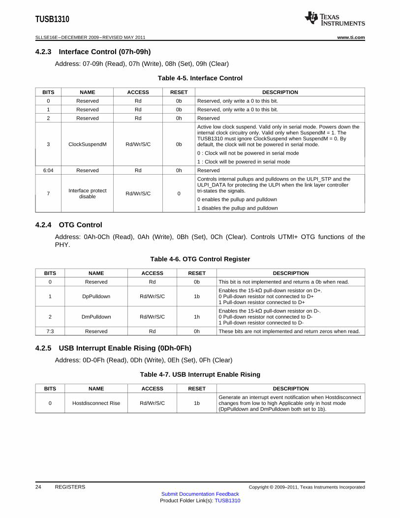
4.2.3 Interface Control (07h-09h) .................................................................................... 24
4.2.4 OTG Control ..................................................................................................... 24
4.2.5 USB Interrupt Enable Rising (0Dh-0Fh) ..................................................................... 24
4.2.6 USB Interrupt Enable Falling (10h-12h) ..................................................................... 25
4.2.7 USB Interrupt Status (13h) .................................................................................... 25
2 Contents Copyright © 2009–2011, Texas Instruments Incorporated

TUSB1310
www.ti.com SLLSE16E–DECEMBER 2009–REVISED MAY 2011
4.2.8 USB Interrupt Latch (14h) ..................................................................................... 25
4.2.9 Debug (15h) ..................................................................................................... 25
4.2.10 Scratch Register (16-18h) ..................................................................................... 255 DESIGN GUIDELINES ......................................................................................................... 26
5.1 Chip Connection on PCB ................................................................................................. 26
5.1.1 USB Connector Pins Connection ............................................................................. 26
5.1.2 Clock Connections .............................................................................................. 275.2 Clock Source Requirements ............................................................................................. 28
5.2.1 Clock Source Selection Guide ................................................................................ 28
5.2.2 Oscillator ......................................................................................................... 29
5.2.3 Crystal ............................................................................................................ 296 ELECTRICAL SPECIFICATIONS .......................................................................................... 30
6.1 ABSOLUTE MAXIMUM RATINGS ...................................................................................... 30
6.2 RECOMMENDED OPERATING CONDITIONS ....................................................................... 30
6.3 DC CHARACTERISTICS FOR 1.8-V DIGITAL IO .................................................................... 30
6.4 DEVICE POWER CONSUMPTION ..................................................................................... 316.5 AC Characteristics ......................................................................................................... 31
6.5.1 Power Up and Reset Timing .................................................................................. 31
6.5.2 PIPE Transmit ................................................................................................... 32
6.5.3 PIPE Receive ................................................................................................... 32
6.5.4 ULPI Parameters ............................................................................................... 33
6.5.5 ULPI Clock ....................................................................................................... 33
6.5.6 ULPI Transmit ................................................................................................... 33
6.5.7 ULPI Receive Timing ........................................................................................... 346.5.8 Power State Transition Time .................................................................................. 34
Copyright © 2009–2011, Texas Instruments Incorporated Contents 3

TUSB1310
SLLSE16E–DECEMBER 2009–REVISED MAY 2011 www.ti.com
List of Figures1-1 Typical Application................................................................................................................. 8
1-2 Functional Block Diagram ........................................................................................................ 9
3-1 Power Up Sequence ............................................................................................................. 18
5-1 Analog Pin Connections ......................................................................................................... 26
5-2 USB Standard-A Connector Pin Connection ................................................................................. 27
5-3 USB Standard-B Connector Pin Connection ................................................................................. 27
5-4 Typical Crystal Connections .................................................................................................... 28
6-1 Power Up and Reset Timing.................................................................................................... 31
6-2 PIPE Transmit Timing ........................................................................................................... 32
6-3 PIPE Receive Timing ............................................................................................................ 32
6-4 ULPI Transmit Timing............................................................................................................ 34
6-5 ULPI Receive Timing ............................................................................................................ 34
4 List of Figures Copyright © 2009–2011, Texas Instruments Incorporated

TUSB1310
www.ti.com SLLSE16E–DECEMBER 2009–REVISED MAY 2011
List of Tables2-1 Configuration Pins................................................................................................................ 10
2-2 PIPE Signal Description ......................................................................................................... 10
2-3 ULPI Signal Description ......................................................................................................... 13
2-4 ULPI Synchronous and Low Power Mode Functions........................................................................ 13
2-5 Clock Signal Name Description ................................................................................................ 14
2-6 JTAG Signal Name Description ................................................................................................ 14
2-7 Reset and Output Control Signal Description ................................................................................ 14
2-8 Strapping Options ................................................................................................................ 14
2-9 USB Interface Signal Name Descriptions ..................................................................................... 15
2-10 Special Connect Signal Descriptions .......................................................................................... 15
2-11 Power/Ground Signal Descriptions ............................................................................................ 15
3-1 Pin States in Chip Reset ........................................................................................................ 17
3-2 Power States...................................................................................................................... 19
3-3 PIPE Control Pin Matrix ......................................................................................................... 19
3-4 RX_STATUS - SKP .............................................................................................................. 20
3-5 RX_STATUS - Receiver Detection............................................................................................. 20
3-6 8b/10b Decode Errors ........................................................................................................... 21
3-7 Elastic Buffer Errors.............................................................................................................. 21
3-8 Disparity Errors ................................................................................................................... 21
4-1 Register Definitions .............................................................................................................. 22
4-2 Register Map...................................................................................................................... 22
4-3 Vendor ID and Product ID....................................................................................................... 23
4-4 Function Control .................................................................................................................. 23
4-5 Interface Control.................................................................................................................. 24
4-6 OTG Control Register............................................................................................................ 24
4-7 USB Interrupt Enable Rising .................................................................................................... 24
4-8 USB Interrupt Enable Falling ................................................................................................... 25
4-9 USB Interrupt Status ............................................................................................................. 25
4-10 USB Interrupt Latch .............................................................................................................. 25
4-11 Debug .............................................................................................................................. 25
4-12 Scratch Register.................................................................................................................. 25
5-1 Oscillator Specification .......................................................................................................... 29
5-2 Oscillator Specification .......................................................................................................... 29
6-1 Power Up and Reset Timing.................................................................................................... 32
6-2 PIPE Transmit Timing ........................................................................................................... 32
6-3 PIPE Receive Timing ............................................................................................................ 32
6-4 ULPI Parameters ................................................................................................................. 33
6-5 ULPI Clock Parameters ......................................................................................................... 33
6-6 ULPI Transmit Timing............................................................................................................ 34
6-7 ULPI Transmit Timing............................................................................................................ 34
Copyright © 2009–2011, Texas Instruments Incorporated List of Tables 5
TUSB1310
SLLSE16E–DECEMBER 2009–REVISED MAY 2011 www.ti.com
6 List of Tables Copyright © 2009–2011, Texas Instruments Incorporated

TUSB1310
www.ti.com SLLSE16E–DECEMBER 2009–REVISED MAY 2011
USB 3.0 TransceiverCheck for Samples: TUSB1310
1 PRODUCT OVERVIEW
1.1 Features1• Universal Serial Bus (USB)
– Single Port 5.0-Gbps USB 3.0 Physical Layer Transceiver• One 5.0-Gbps SuperSpeed Conneciton• One 480-Mbps HS/FS/LS Connection
– Fully Compliant with USB 3.0 Specification– Supports 3+ Meters USB 3.0 Cable Length– Fully Adaptive Equalizer to Optimize Receiver Sensitivity– PIPE to Link Layer Controller
• Supports 16-Bit SDR Mode at 250 MHz• Compliant With PHY Interface for the USB Architectures (PIPE), Version 3.0
– ULPI to Link Layer Controller• Supports 8-Bit SDR Mode at 60 MHz• Supports Synchronous Mode and Low Power Mode• Compliant with UTMI+ Low Pin Interface (ULPI) Specification, Revision 1.1
• General Features– IEEE 1149.1 JTAG Support– IEEE 1149.6 JTAG support for the SuperSpeed Port– Operates on a Single Reference Clock Selectable from 20, 25, 30 or 40 MHz– 3.3-, 1.8-, and 1.1-V Supply Voltages– 1.8-V PIPE and ULPI I/O– Available in Lead-Free 175-Ball 12- x 12-nF BGA Package (175ZAY)
1.2 Target Applications• Surveillance Cameras• Multimedia Handset• Smartphone• Digital Still Camera• Portable Media Player• Personal Navigation Device• Audio Dock• Video IP Phone• Wireless IP Phone• Software Defined Radio
1
Please be aware that an important notice concerning availability, standard warranty, and use in critical applications of TexasInstruments semiconductor products and disclaimers thereto appears at the end of this data sheet.
PRODUCTION DATA information is current as of publication date. Copyright © 2009–2011, Texas Instruments IncorporatedProducts conform to specifications per the terms of the TexasInstruments standard warranty. Production processing does notnecessarily include testing of all parameters.

TUSB1310
SLLSE16E–DECEMBER 2009–REVISED MAY 2011 www.ti.com
1.3 Introduction
The TUSB1310 is a single port, 5.0-Gbps USB 3.0 physical layer transceiver operating off of a singlecrystal or an external reference clock. The reference clock frequencies are selectable from 20, 25, 30, and40 MHz. The TUSB1310 provides a clock to USB link layer controllers. The single reference clock allowsthe TUSB1310 to provide a cost effective USB 3.0 solution with few external components and a minimumimplementation cost.
Link controller interfaces to the TUSB1310 are via a PIPE (SuperSpeed) and a ULPI (USB2.0) interface.The 16-bit PIPE operates with a 250-MHz interface clock. The ULPI supports 8-bit operations with a60-MHz interface clock.
USB 3.0 reduces active power and idle power by improving power management. The PIPE interfacecontrols the TUSB1310 low power states which minimizes power consumption.
SuperSpeed USB leverages existing USB software infrastructure by keeping the existing softwareinterfaces and software drivers. In addition the SuperSpeed USB retains backward compatibility at theType-A connector with USB2.0 based PCs and with USB2.0 cables.
Figure 1-1. Typical Application
1.4 Functional Block Diagram
The USB physical layer handles the low level USB protocol and signaling. This includes data serializationand deserialization, 8b/10b encoding, analog buffers, elastic buffers and receiver detection. It shifts theclock domain of the data from the USB rate to one that is compatible with the link layer controller.
The SuperSpeed USB contains SSTXP/SSTXN and SSRXP/SSRXP differential pairs and uses the PIPEto communicate with the link layer controller. The Non-SuperSpeed USB has a DP/DM differential pair andcommunicates with the link layer controller via the ULPI. The TUSB1310 reference clock is connected toan internal crystal oscillator, spread spectrum clock and PLL which provides clocks to all blocks and to theCLKOUT pin for the link layer controller.
A JTAG interface is used for IEEE1149.1 and IEEE1149.6 boundary scan.
8 PRODUCT OVERVIEW Copyright © 2009–2011, Texas Instruments Incorporated
Submit Documentation FeedbackProduct Folder Link(s): TUSB1310

TUSB1310
www.ti.com SLLSE16E–DECEMBER 2009–REVISED MAY 2011
Figure 1-2. Functional Block Diagram
Copyright © 2009–2011, Texas Instruments Incorporated PRODUCT OVERVIEW 9Submit Documentation FeedbackProduct Folder Link(s): TUSB1310

TUSB1310
SLLSE16E–DECEMBER 2009–REVISED MAY 2011 www.ti.com
2 PIN DESCRIPTIONS
TYPE DESCRIPTION
I Input
O Output
I/O Input/output
PD, PU Internal pull-down / pull-up
S Strapping pin
P Power Supply
G Ground
2.1 Configuration Pins
The configuration pins are not latched by RESETN.
Table 2-1. Configuration Pins
SIGNAL NAME TYPE PIN NO. MODE NAME DESCRIPTION
PHY_MODE1 I, PD H12 USB Must be set to 0. Operates as USB 3.0 transceiver.
PHY_MODE0 I, PU J12 USB Must be set to 1. Operates as USB 3.0 transceiver.
2.2 PIPE
The TUSB1310 supports 16-bit SDR mode with a 250-MHz clock.
Table 2-2. PIPE Signal Description
SIGNAL NAME TYPE BALL NO. DESCRIPTION
TX_DATA and TX_DATAK clock for source synchronous PIPE. This clock frequency isTX_CLK I K1 the same as PCLK frequency. The rising edge of the clock is the reference for all signals.
TX_DATA15 G2
TX_DATA14 H2
TX_DATA13 H1
TX_DATA12 J2
TX_DATA11 L3
TX_DATA10 L2
TX_DATA9 M2Parallel USB SuperSpeed data input bus.TX_DATA8 M1
I The 16 bits represent 2 symbols of transmit data where TX_DATA7-0 is the first symbol toTX_DATA7 N1 be transmitted, and TX_DATA15-8 is the second symbol.TX_DATA6 P1
TX_DATA5 N2
TX_DATA4 P2
TX_DATA3 N3
TX_DATA2 P3
TX_DATA1 N4
TX_DATA0 P5
TX_DATAK1 G1 Data/Control for the symbols of transmit data. TX_DATAK0 corresponds to the low-byte ofI TX_DATA, TX_DATAK1 to the upper byte.TX_DATAK0 J1
Parallel interface data clock. All data movement across the parallel PIPE is synchronousPCLK O A6 to this clock. This clock operates at 250 MHz. The rising edge of the clock is the reference
for all signals.
10 PIN DESCRIPTIONS Copyright © 2009–2011, Texas Instruments Incorporated
Submit Documentation FeedbackProduct Folder Link(s): TUSB1310

TUSB1310
www.ti.com SLLSE16E–DECEMBER 2009–REVISED MAY 2011
Table 2-2. PIPE Signal Description (continued)
SIGNAL NAME TYPE BALL NO. DESCRIPTION
RX_DATA15 B9
RX_DATA14 A9
RX_DATA13 A8
RX_DATA12 B8
RX_DATA11 B5
RX_DATA10 B4
RX_DATA9 A4Parallel USB SuperSpeed data output bus.RX_DATA8 B3
O The 16 bits represent 2 symbols of receive data where RX_DATA7-0 is the first symbolRX_DATA7 A3 received, and RX_DATA15-8 is the second.RX_DATA6 A2
RX_DATA5 B1
RX_DATA4 C2
RX_DATA3 C1
RX_DATA2 D1
RX_DATA1 D2
RX_DATA0 E2
RX_DATAK1 B7 Data/Control for the symbols of receive data. RX_DATAK0 corresponds to the low-byte ofO RX_DATA, RX_DATAK1 to the upper byte. A value of zero indicates a data byte; a value
RX_DATAK0 A7 of 1 indicates a control byte.
RX_VALID O F1 Active High. Indicates symbol lock and valid data on RX_DATA and RX_DATAK.
CONTROL AND STATUS SIGNALS
PHY_RESETN I, PU J3 Active Low. Resets the transmitter and receiver. This signal is asynchronous.
Active High. Used to tell the PHY to begin a receiver detection operation or to beginTX_DETRX_LPBK I, PD M6 loopback.
TX_ELECIDLE I K3 Active High. Forces TX output to electrical idle depending on the power state.
S, I/O, Active High. While de-asserted with the PHY in P0, P1, P2, or P3, indicates detection ofRX_ELECIDLE F3PD LFPS.
Encodes receiver status and error codes for the received data stream when receivingRX_STATUS2 C7 data.ORX_STATUS1 C6 BIT 2 BIT 1 BIT 0 DESCRIPTION
RX_STATUS0 C5 0 0 0 Received data OK
0 0 1 1 SKP ordered set added
0 1 0 1 SKP ordered set removed
0 1 1 Receiver detected
1 0 0 8B/10B decode error
1 0 1 Elastic buffer overflow
Elastic buffer underflow.1 1 0 This error code is not used if the elasticity buffer is
operating in the nominal buffer empty mode.
1 1 1 Receive disparity error
POWER_DOWN1 G3 Power up and down the transceiver power states.I
POWER_DOWN0 H3 BIT 1 BIT 0 DESCRIPTION
0 0 P0, normal operation
0 1 P1, low recovery time latency, power saving state
1 0 P2, longer recovery time latency, low power state
1 1 P3, lowest power state
When transitioning from P3 to P0, the signaling is asynchronous.
Copyright © 2009–2011, Texas Instruments Incorporated PIN DESCRIPTIONS 11Submit Documentation FeedbackProduct Folder Link(s): TUSB1310

TUSB1310
SLLSE16E–DECEMBER 2009–REVISED MAY 2011 www.ti.com
Table 2-2. PIPE Signal Description (continued)
SIGNAL NAME TYPE BALL NO. DESCRIPTION
Active High. Used to communicate completion of several PHY func-tions including powerS, I/O, management state transitions, rate change, and receiver detection. When this signalPHY_STATUS E3PD transitions during entry and exit from P3 and PCLK is not running, then the signaling is
asynchronous.
PWRPRESENT O H11 Indicates the presence of VBUS
CONFIGURATION PINS
Active High. Used only when transmitting USB compliance pat-terns CP7 or CP8. CausesTX_ONESZEROS I, PD M4 the transmitter to transmit an alternating sequence of 50 - 250 ones and 50 - 250 zeros –
regardless of the state of the TX_DATA interface.
Selects transmitter de-emphasis. When the MAC changes, the TUSB1310 starts toTX_DEEMPH1 K11 transmit with the new setting within 128 ns.I, PD, PUTX_DEEMPH0 L11 BIT 1 BIT 0 DESCRIPTION
0 0 -6 dB de-emphasis
0 1 -3.5 dB de-emphasis
1 0 No de-emphasis
1 1 Reserved
TX_MARGIN2 M11 Selects transmitter voltage levels
TX_MARGIN1 M10 BIT 2 BIT 1 BIT 0 TX_SWING DESCRIPTIONI, PDNormal operating rangeTX_MARGIN0 M9 0 0 0 0 800 mV - 1200 mV
Normal operating range0 0 0 1 400 mV - 700 mV
0 800 mV - 1200 mV0 0 1
1 400 mV - 700 mV
0 700 mV - 900 mV0 1 0
1 300 mV - 500 mV
0 400 mV - 600 mV0 1 1
1 200 mV - 400 mV
1 0 200 mV - 400 mVDon't care
1 1 100 mV - 200 mV
Controls transmitter voltage swing level
TX_SWING I, PD M5 0 Full swing
1 Half swing
Active High. Tells PHY to do a polarity inversion on the received data. Inverted data showup on RX_DATA15-0 within 20 PCLK clocks after RX_POLARITY is asserted.
RX_POLARITY I, PD C8 0 PHY does no polarity inversion.
1 PHY does polarity inversion.
Controls presence of receiver terminations
RX_TERMINATION I, PD D3 0 Terminations removed
1 Terminations present
Controls the link signaling rateRATE I, PU L6
The RATE is always 1.
Selects elasticity buffer operating mode
ELAS_BUF_MODE I, PD C9 0 Nominal half full buffer mode
1 Nominal empty buffer mode
12 PIN DESCRIPTIONS Copyright © 2009–2011, Texas Instruments Incorporated
Submit Documentation FeedbackProduct Folder Link(s): TUSB1310

TUSB1310
www.ti.com SLLSE16E–DECEMBER 2009–REVISED MAY 2011
2.3 ULPI
The ULPI (ultra low pin count interface) is a low pin count USB PHY to a link layer controller interface. TheULPI consists of the interface and the ULPI registers. The TUSB1310 is always the master of the ULPIbus.
Table 2-3. ULPI Signal Description
SIGNAL NAME TYPE BALL NO. DESCRIPTION
60-MHz interface clock. All ULPI signals are synchronous to ULPI_CLK. The ULPI_CLK isULPI_CLK O P11 always a 60-MHz output of the TUSB1310. In low power mode, the ULPI_CLK is not driven.
ULPI_DATA7 N6
ULPI_DATA6 P6
ULPI_DATA5 N7
ULPI_DATA4 P7 Data bus. Driven to 00h by the Link when the ULPI bus is idle.S, I/O, PD 8-bit data timed on rising edge of ULPI_CLKULPI_DATA3 N8
ULPI_DATA2 P8
ULPI_DATA1 P9
ULPI_DATA0 N9
Controls the direction of the ULPI_DATA bus
ULPI_DIR O M7 0 ULPI_DATA lines are inputs
1 ULPI_DATA lines are outputs
Active High. The Link must assert ULPI_STP to signal the end of a USB transmit packet or aregister write operation. The ULPI_STP signal must be asserted in the cycle after the last dataULPI_STP S, I, PU M8 byte is presented on the bus. The ULPI_STP has an internal weak pull-up to safeguardagainst false commands on the ULPI_DATA lines.
Active High. The PHY asserts ULPI_NXT to throttle all data types, except register read dataand the RX CMD. The PHY also asserts ULPI_NXT and ULPI_DIR simultaneously to indicateULPI_NXT O N11 USB receive activity, if ULPI_DIR was previously low. The PHY is not allowed to assertULPI_NXT during the first cycle of the TX CMD driven by the Link.
2.3.1 ULPI Modes
The TUSB1310 supports synchronous mode and low power mode. The default mode is synchronousmode.
The synchronous mode is a normal operation mode. The ULPI_DATA are synchronous to ULPI_CLK. Thelow power mode is used during power down and no ULPI_CLK. The TUSB1310 sets ULPI_DIR to outputand drives LineState signals and interrupts.
Table 2-4. ULPI Synchronous and Low Power Mode Functions
SYNCHRONOUS LOW POWER
ULPI_CLK(OUT)
ULPI_DATA7(I/O)
ULPI_DATA6(I/O)
ULPI_DATA5(I/O)
ULPI_DATA4{I/O}
ULPI_DATA3(I/O) ULPI_INT (OUT)
ULPI_DATA2(I/O)
ULPI_DATA1(I/O) ULPI_LINESTATE1(OUT)
ULPI_DATA0(I/O) ULPI_LINE_STATE0 (OUT)
ULPI_DIR(OUT)
ULPI_STP(IN)
ULPI_NXT(OUT)
Copyright © 2009–2011, Texas Instruments Incorporated PIN DESCRIPTIONS 13Submit Documentation FeedbackProduct Folder Link(s): TUSB1310

TUSB1310
SLLSE16E–DECEMBER 2009–REVISED MAY 2011 www.ti.com
2.4 Clocking
Table 2-5. Clock Signal Name Description
SIGNAL NAME TYPE BALL NO. DESCRIPTION
Crystal Input. This pin is the clock reference input for the TUSB1310. The TUSB1310XI I A12 supports either a crystal unit, or a 1.8-V clock input. Frequencies supported are 20, 25,
30, or 40 MHz.
XO O A11 Crystal output. If a 1.8-V clock input is connected to XI, XO must be left open.
CLKOUT O D10 OOBCLK is driven in U3 mode.
2.5 JTAG Interface
The JTAG Interface is used for board-level boundary scan. All digital IO support IEEE1149.1 boundaryscan and SuperSpeed differential pairs support IEEE1149.6 boundary scan.
Table 2-6. JTAG Signal Name Description
SIGNAL NAME TYPE BALL NO. DESCRIPTION
JTAG_TCK I, PU G11 JTAG test clock
JTAG_TMS I, PU D11 JTAG test mode select
JTAG_TDI I, PU E11 JTAG test data input
JTAG_TRSTN I, PD E12 JTAG test asynchronous reset. Active Low.
JTAG_TDO O F11 JTAG test data output
2.6 Reset and Output Control Interface
Table 2-7. Reset and Output Control Signal Description
SIGNAL NAME TYPE BALL NO. DESCRIPTION
RESETN I J11 Active Low. Resets the transmitter and receiver. This signal is asynchronous.
Active High. This can be connected to a 1.8-V power on reset signal on the PCB inorder to avoid static current and signal contention during power up.
OUT_ENABLE I L10 0: Disable all driver outputs while IO powers are supplied, but internal control circuitpowers are not present during power up.1: Enable all driver outputs during normal operation.
2.7 Strap Options
Strapping pins are latched by reset de-assertion in the TUSB1310.
Table 2-8. Strapping Options
SIGNAL NAME TYPE BALL NO. DESCRIPTION
Selects an input clock sourceXTAL_DIS S, I/O, PD F3 0 Crystal Input(RX_ELECIDLE)
1 Clock Input
Selects PIPEPIPE_16BIT S, I/O, PD E3 0 16-bit PIPE SDR mode(PHY_STATUS)
Must be 0 at reset.
Active High. Puts PIPE into isolate mode. When in the isolate mode, TUSB1310 doesnot respond to packet data present at TX_DATA15-0, TXDATAK1-0 inputs and presentsa high imped-ance on the PCLK, RX_DATA15-0, RX_DATAK1-0, RX_VALID outputs.ISO_START S, I/O, PD N6 When in the isolate mode, the TUSB1310 will continue to respond to ULPI. Once the(ULPI_DATA7) isolate mode bit in ULPI register is cleared, the USB interfaces will start transmittingpacket data on TX_DATA15-0 and driving PCLK, RX_DATA15-0, RX_DATA1-0, andRX_VALID.
14 PIN DESCRIPTIONS Copyright © 2009–2011, Texas Instruments Incorporated
Submit Documentation FeedbackProduct Folder Link(s): TUSB1310

TUSB1310
www.ti.com SLLSE16E–DECEMBER 2009–REVISED MAY 2011
Table 2-8. Strapping Options (continued)
SIGNAL NAME TYPE BALL NO. DESCRIPTION
Selects ULPI data bus bit widthULPI_8BIT S, I/O, PD P6 0 8-bit ULPI SDR mode(ULPI_DATA6)
Must be set to 0.
Select input reference clock frequency for on-chip oscillator
REFCLKSEL1, 00 20 MHz on XIREFCLKSEL0 N7S, I/O, PD 01 25 MHz on XI(ULPI_DATA5, P7
10 30 MHz on XIULPI_DATA4)
11 40 MHz on XI
2.8 USB Interfaces
Table 2-9. USB Interface Signal Name Descriptions
SIGNAL NAME TYPE BALL NO. DESCRIPTION
SSTXP H14O USB SuperSpeed transmitter differential pair
SSTXM J14
SSRXP E14I USB SuperSpeed receiver differential pair
SSRXM F14
DP P14I/O USB non-SuperSpeed differential pair
DM P13
USB VBUS pinVBUS I N12 Connected through an external voltage divider.
2.9 Special Connect
Table 2-10. Special Connect Signal Descriptions
SIGNAL NAME TYPE BALL NO. DESCRIPTION
High precision external resistor used for calibration. The R1 value shall be 10 kΩ ±1%R1EXT O L14 accuracy.
R1EXTRTN I L13 R1 ground reference. This pin is not connected to board ground.
CEXT O M14 Connected to an external 4.7-nF capacitor
CEXTSS O A14 Connected to an external 4.7-nF capacitor
D6
D5
C13RSVD I/O Must be left open.
C14
K4
J4
2.10 Power and Ground
Table 2-11. Power/Ground Signal Descriptions
SIGNAL NAME TYPE BALL NO. DESCRIPTION
VDDA3P3 P P12 Analog 3.3-V power supply
N14
VDDA1P8 P A13 Analog 1.8-V power supply
C10
Copyright © 2009–2011, Texas Instruments Incorporated PIN DESCRIPTIONS 15Submit Documentation FeedbackProduct Folder Link(s): TUSB1310

TUSB1310
SLLSE16E–DECEMBER 2009–REVISED MAY 2011 www.ti.com
Table 2-11. Power/Ground Signal Descriptions (continued)
SIGNAL NAME TYPE BALL NO. DESCRIPTION
C12
K14
G13VDDA1P1 P Analog 1.1-V power supply
G14
D14
C11
B2 C3
D4 D7
D8 D9
E4 F4VDD1P8 P Digital IO 1.8-V power supply
G4 H4
L5 L4
M3 L7
L8 L9
A5 A10
B6 B10
E1 F2
K2 L1VDD1P1 P Digital 1.1-V power supply
N5 P4
N10 P10
K13 D13
C4
B14 B13
J13 H13
F13 E13
K12 L12
VSSA G G12 Analog ground
D12
N13
M12
M13
Oscillator groundIf using a crystal, this should not be connected to PCB ground plane.VSSOSC G B12 See Chapter 5 for guidelines.If using an oscillator, this should be connected to PCB ground.
F6 F7
F8 F9
G6 G7
G8 G9
VSS G J6 J7 Digital ground
H6 H7
H8 H9
J8 J9
B11 F12
16 PIN DESCRIPTIONS Copyright © 2009–2011, Texas Instruments Incorporated
Submit Documentation FeedbackProduct Folder Link(s): TUSB1310

TUSB1310
www.ti.com SLLSE16E–DECEMBER 2009–REVISED MAY 2011
3 FUNCTIONAL DESCRIPTION
3.1 Power On and Reset
The TUSB1310 has two hardware reset pins, a chip reset RESETN and a logic reset PHY_RESETN. TheRESETN is used only at Power On. The PHY_RESETN can be used as a functional reset. The ULPIregister also has a software reset.
Until all power sources are supplied, the OUT_ENABLE pin can control the output driver enable. After allpower sources are supplied, the chip reset RESETN and a ULPI soft reset will be asserted by the linklayer. The power up sequence is described in section 3.1.4.
3.1.1 RESETN and PHY_RESETN – Hardware Reset
The RESETN sets all internal states to initial values. The link layer needs to hold the PHY in reset via theRESETN until all power sources and the reference clock to the TUSB1310 are stable. All pins used forstrapping options must be set before RESETN de-assertion. All strapping option pins have internal pull-upor pull-down to set default values, but if any non-default values are desired, they need to be controlledexternally by the link layer controller.
Table 3-1. Pin States in Chip Reset
PIPE CONTROL STATE VALUEPIN NAME
TX_DETRX_LPBK Inactive 0
TX_ELECIDLE Active 1
TX_COMPLIANCE Inactive 0
RX_POLARITY Inactive 0
POWER_DOWN U2 10b
TX_MARGIN2-0 Normal operating range 000b
TX_DEEMP -3.5 dB 1
RATE 5.0 Gbps 1
TX_SWING Full swing or half swing 0 or 1
RX_TERMINATION Appropriate state 0 or 1
3.1.2 ULPI Reset – Software Reset
After power-up, the link layer controller must set the Reset bit in ULPI register. It resets the core but doesnot reset the ULPI interface or the ULPI registers.
During the ULPI reset, the ULPI_DIR is de-asserted. After the reset, the ULPI_DIR is asserted again andthe TUSB1310 sends an RX CMD update to the link layer. During the reset, the link should ignore signalson the ULPI_DATA7-0 and must not access the TUSB1310.
3.1.3 OUT_ENABLE - Output Enable
Digital IO buffers use two power supplies, core VDD1P1 and IO VDD1P8. During power up,OUT_ENABLE must be asserted low for proper operation.
3.1.4 Power Up Sequence
The power up sequence is shown in Figure 3-1.
Copyright © 2009–2011, Texas Instruments Incorporated FUNCTIONAL DESCRIPTION 17Submit Documentation FeedbackProduct Folder Link(s): TUSB1310

Power Supplies
XI
RESETN
PCLK
ULPI_CLK
Internal resetn/
PLL_EN/SUSPENDM
Internal latched
strapping pin statesLatched data
PHY_STATUS/ULPI_DIR
300ms
TUSB1310
SLLSE16E–DECEMBER 2009–REVISED MAY 2011 www.ti.com
Figure 3-1. Power Up Sequence
After proper power supply sequencing, the reference clock on XI starts to operate. On the RESETNde-assertion, REFCLKSEL1-0 is determined depending on the PHY_MODE pins, PLL is locked and thevalid ULPI_CLK and the valid PCLK are driven.
After all stable clocks are provided, the TUSB1310 allows the link layer controller to access byde-asserting the ULPI_DIR. The link layer controller sets the Reset bit in the ULPI register. At the PIPEin-terface, the PHY_STATUS changes from high to low in order to indicate the TUSB1310 is in the powerstate specified by the POWER_DOWN signal. After the PHY_STATUS change, the TUSB1310 is readyfor PIPE transactions.
3.2 Clocks
3.2.1 Clock Distribution
A source clock should be provided via XI/XO from an external crystal or from a square wave clock. TheUSB3.0 PLL provides a clock to the PIPE which drives 250 MHz. The USB2.0 PLL provides a 60-MHzclock to the ULPI.
3.2.2 Output Clock
The CLKOUT is used by the link layer controller or the MAC. When ClkoutEn bit at the ULPI SS USBregister is set low, a 120-MHz clock is available via the CLKOUT only in the USB U3 power state. If theClkoutEn bit is set high, the 250-MHz clock is driven via CLKOUT in all power states.
3.3 Power Management
The SuperSpeed USB power state transition is controlled by the PIPE POWER_DOWN1-0 and thenon-SuperSpeed USB power state is transitioned by setting suspendM bit in the ULPI Function controlregister via the ULPI or by asserting the ULPI_STP.
18 FUNCTIONAL DESCRIPTION Copyright © 2009–2011, Texas Instruments Incorporated
Submit Documentation FeedbackProduct Folder Link(s): TUSB1310

TUSB1310
www.ti.com SLLSE16E–DECEMBER 2009–REVISED MAY 2011
3.3.1 USB Power Management
The USB 3.0 specification improves power consumption by defining 4 power states, U0, U1, U2, and U3while the PIPE specification defines P0, P1, P2 and P3. The POWER_DOWN pin states are mapped toLTSSM states as described in Table 2-10. For all power state transitions, the link layer controller must notbegin any operational sequences or further power state transitions until the TUSB1310 has indicated thatthe internal state transition is completed.
Table 3-2. Power States
PIPE USB POWERPOWER PCLK PLL TRANSMITTING RECEIVING PHY_STATUSSTATESTATE
U0, all other LTSSM A single cycleP0 On On Active or Idle or LFPS Active or Idlestates assertion
A single cycleP1 U1 On On Idle or LFPS Idle assertion
U2, RxDetect, A single cycleP2 On On Idle or LFPS or RxDetect IdleSS.Inactive assertion
PHY_STATUS isOff. The asserted beforePIPE is in PCLK is turned offP3 U3, SS.disabled an Off LFPS or RxDetect Idle and deassertedasynchrono when PCLK is fullyus mode off.
When the link layer controller wants to transmit LFPS in P1, P2, or P3 state, it must de-assertTX_ELECIDLE. The TUSB1310 generates valid LFPS until the TX_ELECIDLE is asserted. The link layercontroller must assert TX_ELECIDLE before transitioning to P0.
When RX_ELECIDLE is de-asserted in P0, P1, P2, or P3, the TUSB1310 receiver monitors for LFPSexcept during reset or when RX_TERMINATION is removed for electrical idle.
When the TUSB1310 is in P0 and is actively transmitting; only RX_POLARITY can be asserted.
Table 3-3. PIPE Control Pin Matrix
POWER STATE TX_DETRX_LPBK TX_ELECIDLE DESCRIPTION
0 0 Transmitting data on TX_DATA
0 1 Not transmitting and is in electrical idle.P0
1 0 Goes into loopback mode
1 1 Transmits LFPS signaling
0 Transmits LFPS signalingP1 Don't care
1 Not transmitting and is in electrical idle.
Don't care 0 Transmits LFPS signaling
P2 0 1 Idle
1 1 Does a receiver detection operation
0 Transmits LFPS signalingP3 Don't care
1 Does a receiver detection operation
3.4 Receiver Status
The TUSB1310 has an elastic buffer for clock tolerance compensation, the link partner detection, andsome received data error detections. The receive data status from SSRXP/SSRXN differential pairpresents on RX_STATUS2-0. If an error occurs during a SKP ordered set, the error signaling hasprecedence. If more than one error occurs on a received byte, the errors have the priority below.
1. 8B/10B decode error
2. Elastic buffer overflow
Copyright © 2009–2011, Texas Instruments Incorporated FUNCTIONAL DESCRIPTION 19Submit Documentation FeedbackProduct Folder Link(s): TUSB1310

TUSB1310
SLLSE16E–DECEMBER 2009–REVISED MAY 2011 www.ti.com
3. Elastic buffer underflow (can not occur in nominal empty buffer model)
4. Disparity error
3.4.1 Clock Tolerance Compensation
The receiver contains an elastic buffer used to compensate for differences in frequencies between bitrates at the two ends of a link. The elastic buffer must be capable of holding enough symbols to handleworst case differences in frequency and worst case intervals between SKP ordered sets. A SKP order setis a set of symbols transmitted as a group. The SKP ordered sets allows the receiver to adjust the datastream being received to prevent the elastic buffer from either overflowing or under-flowing due to anyclock tolerance differences.
The TUSB1310 supports two models, nominal half full buffer model and nominal empty buffer mode. Forthe nominal half full buffer model, the TUSB1310 monitors the receive data stream. When a Skip orderedset is received, the TUSB1310 adds or removes one SKP order set from each SKP to manage its elasticbuffer to keep the buffer as close to half full as possible. Only full SKP ordered sets are added orremoved. When a SKP order set is added, the TUSB1310 asserts an “Add SKP” code (001b) on theRX_STATUS for one clock cycle. When a SKP order set is removed, the RX_STATUS is has a “RemoveSHP” code (010b).
For the nominal empty buffer model the TUSB1310 attempts to keep the elasticity buffer as close to emptyas possible. When no SKP ordered sets have been received, the TUSB1310 will be required to insert SKPordered sets into the received data stream.
Table 3-4. RX_STATUS - SKP
RX_STATUS2-0 SKP ADDITION or REMOVAL LENGTH
001b 1 SKP ordered set addedOne clock cycle
010b 1 SKP ordered set removed
3.4.2 Receiver Detection
TX_DETRX_LPBK starts a receiver detection operation to determine if there is a receiver at the other endof the link. When the receiver detect sequence completes, the PHY_STATUS is asserted for one clockand drives the RX_STATUS signals to the appropriate code. Once the TX_DETRX_LPBK signal isasserted, the link layer controller must leave the signal asserted until the PHY_STATUS pulse. Whenreceiver detection is performed in P3, the PHY_STATUS shows the appropriate receiver detect value untilthe TX_DETRX_LPBK is de-asserted.
Table 3-5. RX_STATUS - Receiver Detection
RX_STATUS2-0 DETECTED CONDITION LENGTH
000b Receiver not presentOne clock cycle
011b Receiver present
3.4.3 8b/10b Decode Errors
When the TUSB1310 detects an 8b/10b decode error, it will assert an EDB (0xFE) symbol in the data onthe RX_DATA where the bad byte occurred. In the same clock cycle that the EDB symbol is asserted onthe RX_DATA, the 8b/10b decode error code (100b) will be asserted on the RX_STATUS. 8b/10bdecoding error has priority over all other receiver error codes and could mask out a disparity erroroccurring on the other byte of data being clocked onto the RX_DATA with the EDB symbol.
20 FUNCTIONAL DESCRIPTION Copyright © 2009–2011, Texas Instruments Incorporated
Submit Documentation FeedbackProduct Folder Link(s): TUSB1310

TUSB1310
www.ti.com SLLSE16E–DECEMBER 2009–REVISED MAY 2011
Table 3-6. 8b/10b Decode Errors
RX_STATUS2-0 DETECTED ERROR LENGTH
Clock cycles during the effected byte is100b 8B/10B decode error transferred on RX_DATA15-0
3.4.4 Elastic Buffer Errors
When the elastic buffer overflows, data is lost during the reception of the data. The elastic buffer overflowerror code (101b) will be asserted on the RX_STATUS on the PCLK cycle the omitted data would havebeen asserted. The data asserted on the RX_DATA is still valid data, the elastic buffer overflow error codeon the RX_STATUS just marks a discontinuity point in the data stream being received.
When the elastic buffer underflows, EDB (0xFE) symbols are inserted into the data stream on theRX_DATA to fill the holes created by the gaps between valid data. For every PCLK cycle a EDB symbol isasserted on the RX_DATA, an elastic buffer underflow error code (111b) is asserted on the RX_STATUS.In nominal empty buffer mode, SKP ordered sets are transferred on RX_DATA and the underflow is notsignaled.
Table 3-7. Elastic Buffer Errors
RX_STATUS2-0 DETECTED ERROR LENGTH
Clock cycles the omitted data would have101b Elastic buffer overflow appeared
Clock cycles during the EDB symbol110b Elastic buffer underflow presence on RX_DATA15-0
3.4.5 Disparity Errors
When the TUSB1310 detects a disparity error, it will assert a disparity error code (111b) on theRX_STATUS in the same PCLK cycle it asserts the erroneous data on the RX_DATA. The disparity codedoes not discern which byte on the RX_DATA is the erroneous data.
Table 3-8. Disparity Errors
RX_STATUS2-0 DETECTED ERROR LENGTH
Clock cycles during the ef-fected byte is111b Disparity error transferred on RX_DATA15-0
3.5 Loopback
The TUSB1310 begins an internal loopback operation from SSRXP/SSRXN differential pairs toSSTXP/SSTXN differential pairs when the TX_DETRX_LPBK is asserted while holding TX_ELECIDLEde-asserted. The TUSB1310 will stop transmitting data to the SSTXP/SSTXN signaling pair from theTX_DATA and begin transmitting on the SSTXP/SSTXN signaling pair the data received at theSSRXP/SSRXN signaling pair. This data is not routed through the 8b/10b coding/encoding paths. While inthe loopback operation, the received data is still sent to the RX_DATA. The data sent to the RX_DATA isrouted through the 10b/8b decoder.
The TX_DETRX_LPBK de-assertion will terminate the loopback operation and return to transmittingTX_DATA over the SSTXP/SSTXN signaling pair. The TUSB1310 only transitions out of loopback ondetection of LFPS signaling by transitioning to P2 state and starting the LFPS handshake.
Copyright © 2009–2011, Texas Instruments Incorporated FUNCTIONAL DESCRIPTION 21Submit Documentation FeedbackProduct Folder Link(s): TUSB1310

TUSB1310
SLLSE16E–DECEMBER 2009–REVISED MAY 2011 www.ti.com
4 REGISTERS
4.1 Register Definitions
Table 4-1. Register Definitions
ACCESS CODE EXPANDED NAME DESCRIPTION
Rd Read Register can be read. Read only if this is the only mode given.
Wr Write Pattern on the data bus will be written over all bits of the register.
S Set Pattern on the data bus is OR'ed with and written into the register.
Pattern on the data bus is a mask. If a bit in the mask is set, then theC Clear corresponding register bit will be set to zero(cleared).
4.2 Register Map
The TUSB1310 contains the ULPI registers consisting of an immediate register set and an extendedregister set.
Table 4-2. Register Map
ADDRESS (6 BITS)REGISTER NAME
Rd Wr Set Clr
IMMEDIATE REGISTER SET
Vendor ID low 00h
Vendor ID high 01h
Product ID low 02h
Product ID high 03h
Function control 04h-06h 04h 05h 06h
Interface control 07h-09h 07h 08h 09h
OTG Control 0Ah-0Ch 0Ah 0Bh 0Ch
USB Interrupt Enable Rising 0Dh-0Fh 0Dh 0Eh 0Fh
USB Interrupt Enable Falling 10h-12h 10h 11h 12h
USB Interrupt Status 13h 13h
USB Interrupt Latch 14h 14h
Debug 15h
Scratch register 16h-18h 16h 17h 18h
Reserved 19h-2Eh
22 REGISTERS Copyright © 2009–2011, Texas Instruments Incorporated
Submit Documentation FeedbackProduct Folder Link(s): TUSB1310

TUSB1310
www.ti.com SLLSE16E–DECEMBER 2009–REVISED MAY 2011
4.2.1 Vendor ID and Product ID (00h-03h)
Table 4-3. Vendor ID and Product ID
ADDRESS BITS NAME ACCESS RESET DESCRIPTION
00h 7:00 Vendor ID low Rd 51h Lower byte of vendor ID supplied by USB-IF
01h 7:00 Vendor ID high Rd 04h Upper byte of vendor ID supplied by USB-IF
02h 7:00 Product ID low Rd 10h Lower byte of vendor ID supplied by vendor
03h 7:00 Product ID high Rd 13h Upper byte of vendor ID supplied by vendor
4.2.2 Function Control (04h-06h)
Address: 04h-06h (Read), 04h (Write), 05h (Set), 06h (Clear)
Table 4-4. Function Control
BITS NAME ACCESS RESET DESCRIPTION
Selects the required transceiver speed
00b : Enable HS transceiver
01b: Enable FS transceiver1:00 XcvrSelect Rd/Wr/S/C 1h
10b: Enable LS transceiver
11b: Enable FS transceiver for LS packets
(FS preamble is automatically pre-pended)
Controls the internal 1.5-kΩ pullup resister and 45-Ω HS terminations.Control over bus resistors changes depending on XcvrSelect,
2 TermSelect Rd/Wr/S/C 0 OpMode, DpPulldown and DmPulldown. Since low speed peripheralsnever support full speed or hi-speed, providing the 1.5 kΩ on DM forlow speed is optional.
Selects the required bit encoding style during transmit
00 : Normal operation
01: Non-driving4:03 OpMode Rd/Wr/S/C 010: Disable bit-stuff and NRZI encoding
11: Do not automatically add SYNC and EOP when transmitting. Mustbe used only for HS packets.
Active High transceiver reset. After the Link sets this bit, theTUSB1310 must assert the ULPI_DIR and reset the ULPI. When thereset is completed, the PHY de-asserts the ULPI_DIR andautomatically clears this bit. After de-asserting the ULPI_DIR, the PHY5 Reset Rd/Wr/S/C 0 must re-assert the ULPI_DIR and send an RX CMD update on the linklayer controller. The link layer controller must wait for the ULPI_DIR tode-assert before using the ULPI bus. Does not reset the ULPI or ULPIregister set.
Active low PHY suspend. Put the TUSB1310 into low power mode.The PHY can power down all blocks except the full speed receiver,OTG comparators, and the ULPI pins. The PHY must automatically set
6 SuspendM Rd/Wr/S/C 1h this bit to '1' when low power mode is exited.
0: Low power mode
1: Powered
7 Reserved Rd 0 Reserved
Copyright © 2009–2011, Texas Instruments Incorporated REGISTERS 23Submit Documentation FeedbackProduct Folder Link(s): TUSB1310
TUSB1310
SLLSE16E–DECEMBER 2009–REVISED MAY 2011 www.ti.com
4.2.3 Interface Control (07h-09h)
Address: 07-09h (Read), 07h (Write), 08h (Set), 09h (Clear)
Table 4-5. Interface Control
BITS NAME ACCESS RESET DESCRIPTION
0 Reserved Rd 0b Reserved, only write a 0 to this bit.
1 Reserved Rd 0b Reserved, only write a 0 to this bit.
2 Reserved Rd 0h Reserved
Active low clock suspend. Valid only in serial mode. Powers down theinternal clock circuitry only. Valid only when SuspendM = 1. TheTUSB1310 must ignore ClockSuspend when SuspendM = 0. By
3 ClockSuspendM Rd/Wr/S/C 0b default, the clock will not be powered in serial mode.
0 : Clock will not be powered in serial mode
1 : Clock will be powered in serial mode
6:04 Reserved Rd 0h Reserved
Controls internal pullups and pulldowns on the ULPI_STP and theULPI_DATA for protecting the ULPI when the link layer controller
Interface protect tri-states the signals.7 Rd/Wr/S/C 0disable 0 enables the pullup and pulldown
1 disables the pullup and pulldown
4.2.4 OTG Control
Address: 0Ah-0Ch (Read), 0Ah (Write), 0Bh (Set), 0Ch (Clear). Controls UTMI+ OTG functions of thePHY.
Table 4-6. OTG Control Register
BITS NAME ACCESS RESET DESCRIPTION
0 Reserved Rd 0b This bit is not implemented and returns a 0b when read.
Enables the 15-kΩ pull-down resistor on D+.1 DpPulldown Rd/Wr/S/C 1b 0 Pull-down resistor not connected to D+
1 Pull-down resistor connected to D+
Enables the 15-kΩ pull-down resistor on D-.2 DmPulldown Rd/Wr/S/C 1h 0 Pull-down resistor not connected to D-
1 Pull-down resistor connected to D-
7:3 Reserved Rd 0h These bits are not implemented and return zeros when read.
4.2.5 USB Interrupt Enable Rising (0Dh-0Fh)
Address: 0D-0Fh (Read), 0Dh (Write), 0Eh (Set), 0Fh (Clear)
Table 4-7. USB Interrupt Enable Rising
BITS NAME ACCESS RESET DESCRIPTION
Generate an interrupt event notification when Hostdisconnect0 Hostdisconnect Rise Rd/Wr/S/C 1b changes from low to high Applicable only in host mode
(DpPulldown and DmPulldown both set to 1b).
24 REGISTERS Copyright © 2009–2011, Texas Instruments Incorporated
Submit Documentation FeedbackProduct Folder Link(s): TUSB1310

TUSB1310
www.ti.com SLLSE16E–DECEMBER 2009–REVISED MAY 2011
4.2.6 USB Interrupt Enable Falling (10h-12h)
Address: 10-12h (Read), 10h (Write), 11h (Set), 12h (Clear)
Table 4-8. USB Interrupt Enable Falling
BITS NAME ACCESS RESET DESCRIPTION
Generate an interrupt event notification when Host-disconnect0 Hostdisconnect Fall Rd/Wr/S/C 1b changes from high to low. Applicable only in host.
4.2.7 USB Interrupt Status (13h)
Address: 13h (Read-only)
Table 4-9. USB Interrupt Status
BITS NAME ACCESS RESET DESCRIPTION
Generate an interrupt event notification when Host-disconnect0 Hostdisconnect Fall Rd/Wr/S/C 1b changes from high to low. Applicable only in host.
4.2.8 USB Interrupt Latch (14h)
Address: 14h (Read-only with auto-clear)
Table 4-10. USB Interrupt Latch
BITS NAME ACCESS RESET DESCRIPTION
Set to 1b by the PHY when an unmasked event occurs on0 Hostdisconnect Fall Rd/Wr/S/C 1b Hostdisconnect. Cleared when this register is read.
Applicable only in host mode.
4.2.9 Debug (15h)
Address: 15h (Read-only)
Table 4-11. Debug
BITS NAME ACCESS RESET DESCRIPTION
0 LineState0 Rd 0 Contains the current value of LineState0
1 LineState1 Rd 0 Contains the current value of LineState0
07:2 Reserved Rd 0 Reserved
4.2.10 Scratch Register (16-18h)
Address: 16-18h (Read), 16h (Write), 17h (Set), 18h (Clear)
Table 4-12. Scratch Register
BITS NAME ACCESS RESET DESCRIPTION
Empty register byte for testing purposes. Software can read, write, set,7:0 Scratch Rd/Wr/S/C 00 and clear this register and the TUSB1310 functionality will not be
affected.
Copyright © 2009–2011, Texas Instruments Incorporated REGISTERS 25Submit Documentation FeedbackProduct Folder Link(s): TUSB1310

CEXTSS
CEXT
4 .7nF
VSSA
VSSA
4.7 nF
R1EXT
R1EXTRTN
10KW ± 1 %
SS
RX
P
VBUS
SS
RX
N
SS
TX
P
SS
TX
N DP
DM
USB Connector
XI
VSSOSC
XO
CrystalConnection
ULPIPIPE RX
PIPE TX
Link Controller
JTAGJTAG
10KW ± 1%
90.9KW ± 1 %
TUSB1310
SLLSE16E–DECEMBER 2009–REVISED MAY 2011 www.ti.com
5 DESIGN GUIDELINES
5.1 Chip Connection on PCB
Components should be placed close to the TUSB1310 to reduce the trace length of the interface betweenthe components and the TUSB1310. If external capacitors can not accommodate a close placement,shielding to ground is recommended.
Figure 5-1. Analog Pin Connections
5.1.1 USB Connector Pins Connection
Differential pair signals, DP/DM, SSTXP/SSTXN, SSRXP/SSRXN, should be kept as short as possible.The differential pair traces should be trace-length matched and parallelism should be maintained. Theyalso need to minimize vias and corners and should avoid crossing plane splits and stubs.
Figure 5-2 and Figure 5-3 are for visual reference only.
26 DESIGN GUIDELINES Copyright © 2009–2011, Texas Instruments Incorporated
Submit Documentation FeedbackProduct Folder Link(s): TUSB1310

SSRXP
VBUS
5
6
7
8
9
4
1
3
2
Pin# Signal Name
1
2
3
4
5
6
7
8
9
VBUS
DM
DP
GND
SSRXN
SSRXP
GND_DRAIN
SSTXN
SSTXP
SSRXN
SSTXP
SSTXN
DPDM
90.9kW ± 1%
10kW ± 1%
SSRXP
VBUS
9
8
7
6
5
4
3
1
2
Pin# Signal Name
1
2
3
4
5
6
7
8
9
VBUS
DM
DP
GND
SSTXN
SSTXP
GND_DRAIN
SSRXN
SSRXP
SSRXN
SSTXP
SSTXN
DPDM
90.9kW ± 1%
10kW ± 1%
TUSB1310
www.ti.com SLLSE16E–DECEMBER 2009–REVISED MAY 2011
Figure 5-2. USB Standard-A Connector Pin Connection
Figure 5-3. USB Standard-B Connector Pin Connection
5.1.2 Clock Connections
The TUSB1310 supports an external oscillator source or a crystal unit. If a clock is provided to XI insteadof a crystal, XO is left open. Otherwise, if a crystal is used, the connection needs to follow the guidelinesbelow.
Since XI and XO are coupled to other leads and supplies on the PCB, it is important to keep them as shortas possible and away from any switching leads. It is also recommended to minimize the capacitancebetween XI and XO. This can be accomplished by connecting the VSSOSC lead to the two externalcapacitors CL1 and CL2 and shielding them with the clean ground lines. The VSSOSC should not beconnected to PCB ground.
Copyright © 2009–2011, Texas Instruments Incorporated DESIGN GUIDELINES 27Submit Documentation FeedbackProduct Folder Link(s): TUSB1310

TUSB1310
SLLSE16E–DECEMBER 2009–REVISED MAY 2011 www.ti.com
Load capacitance (Cload) of the crystal varying with the crystal vendors is the total capacitance value ofthe entire oscillation circuit system as seen from the crystal. It includes two external capacitors CL1 andCL2 in Figure 5-4. CVSS below is optional, but recommended for minimum jitter implementation. Thetrace length between the decoupling capacitors and the corresponding power pins on the TUSB1310needs to be minimized. It is also recommended that the trace length from the capacitor pad to the poweror ground plane be minimized.
Figure 5-4. Typical Crystal Connections
5.2 Clock Source Requirements
5.2.1 Clock Source Selection Guide
Reference clock jitter is an important parameter. Jitter on the reference clock will degrade both thetransmit eye and receiver jitter tolerance no matter how clean the rest of the PLL is, thereby impairingsys-tem performance. Additionally, a particularly jittery reference clock may interfere with PLL lockdetection mechanism, forcing the lock detector to issue an unlock signal. A good quality, low jitterreference clock is required to achieve compliance with supported USB3.0 standards. For example,USB3.0 specification requires the random jitter (RJ) component of either RX or TX to be 2.42 ps (randomphase jitter calculated after applying jitter transfer function - JTF). As the PLL typically has a number ofadditional jitter components, the reference clock jitter must be considerably below the overall jitter budget.
28 DESIGN GUIDELINES Copyright © 2009–2011, Texas Instruments Incorporated
Submit Documentation FeedbackProduct Folder Link(s): TUSB1310

TUSB1310
www.ti.com SLLSE16E–DECEMBER 2009–REVISED MAY 2011
5.2.2 Oscillator
If an external clock source is used, XI should be tied to the clock source and XO should be left floating.
Table 5-1. Oscillator Specification
PARAMETER CONDITION MIN TYP MAX UNIT
Frequency tolerance Operational temperature ±50 ppm
Frequency stability 1 year aging ±50 ppm
Rise / Fall time 20% - 80% 6 ns
Reference clock RJ with JTF (1 sigma) (1) (2) 0.8 ps
Reference clock TJ with JTF (total p-p) (2) (3) 25 ps
Reference clock jitter (absolute p-p) (4) 50 ps
(1) Sigma value assuming Gaussian distribution(2) After application of JTF(3) Calculated as 14.1 x RJ + DJ(4) Absolute phase jitter (p-p)
5.2.3 Crystal
Either a 20-MHz, 25-MHz, 30-MHz, or 40-MHz crystal can be selected. A parallel, 20-pF load crystalshould be used if a crystal source is used.
Table 5-2. Oscillator Specification
PARAMETER CONDITION MIN TYP MAX UNIT
Frequency tolerance Operational temperature ±50 ppm
Frequency stability 1 year aging ±50 ppm
Load capacitance 12 20 24 pF
Copyright © 2009–2011, Texas Instruments Incorporated DESIGN GUIDELINES 29Submit Documentation FeedbackProduct Folder Link(s): TUSB1310

TUSB1310
SLLSE16E–DECEMBER 2009–REVISED MAY 2011 www.ti.com
6 ELECTRICAL SPECIFICATIONS
6.1 ABSOLUTE MAXIMUM RATINGSover operating free-air temperature range (unless otherwise noted)
VALUE UNIT
VDD1P1 Digital 1.1 steady-state supply voltage -0.3 to 1.4 V
VDD1P8 Digital IO 1.8 steady-state supply voltage -0.3 to 2.45 V
VDDA1P1 Analog 1.1 steady-state supply voltage -0.3 to 1.4 V
VDDA1P8 Analog 1.8 steady-state supply voltage -0.3 to 2.45 V
VDDA3P3 Analog 3.3 steady-state supply voltage -0.3 to 3.8 V
6.2 RECOMMENDED OPERATING CONDITIONSover operating free-air temperature range (unless otherwise noted)
MIN NOM MAX UNIT
VDDA3P3 Analog 3.3 supply voltage 2.97 3.3 3.63 V
VDDA1P8 Analog 1.8 supply voltage 1.71 1.8 1.98 V
VDDA1P1 Analog 1.1 supply voltage 1.045 1.1 1.155 V
VDD1P8 Digital IO 1.8 supply voltage 1.62 1.8 1.98 V
VDD1P1 Digital 1.1 supply voltage 1.045 1.1 1.155 V
VBUS Voltage at VBUS PAD 0 1.21 V
TA Operating free-air temperature range 0 70 °CTJ Operating junction temperature range -40 105 °C
Human Body Model (HBM) 500ESD VCharged Device Model 500(CDM)
6.3 DC CHARACTERISTICS FOR 1.8-V DIGITAL IOover operating free-air temperature range (unless otherwise noted)
PARAMETER MIN TYP MAX UNIT
0.65 xVIH High-level input voltage VVDDS
0.35 xVIL Low-level input voltage VVDDS
IO = -2 mA, VDDS = 1.62 V to 1.98 V, driver enabled, pullup or VDDS -pulldown disabled 0.45
VOH VIO = -2 mA, VDDS = 1.4 V to 1.6 V, driver enabled, pullup or 0.75 xpulldown disabled VDDS
IO = 2 mA, driver enabled, VDDS = 1.62 V to 1.98 V, pullup or 0.45pulldown disabledVOL V
IO = 2 mA, VDDS = 1.4 V to 1.6 V, driver enabled, pullup or 0.25 xpulldown disabled VDDS
Vhys Input hysteresis 100 270 mV
Any receiver, including those with a pullup or pulldown. TheII ±1 µApullup or pulldown must be disabled.
Receiver/pullup only, pullup enabled (not inhibited), VPAD = 0 V -47 to -169II(PUon) µA
Receiver/pullup only, pullup enabled (not inhibited) -100
IOZ Driver only, driver disabled ±20 µA
IZ(1) ±20 µA
VTX_DIFF_SS SSTXP/SSTXN Differential p-p Tx voltage swing 0.8 1.2 V
(1) IZ is the total leakage current through the PAD connection of a driver/receiver combination that may include a pullup or pulldown. Thedriver output is disabled and the pullup or pulldown is inhibited.
30 ELECTRICAL SPECIFICATIONS Copyright © 2009–2011, Texas Instruments Incorporated
Submit Documentation FeedbackProduct Folder Link(s): TUSB1310

VDD1 P 1
VDD1P 8 and
Analog Power Supplies
OUT_ ENABLE
XI
RESETN
Latch - In of Hardware
Strapping Pins
ULPI _ DIR
Tcfgin 1
Drive Output
Strapping pins
Tcfgin 2
TUSB1310
www.ti.com SLLSE16E–DECEMBER 2009–REVISED MAY 2011
DC CHARACTERISTICS FOR 1.8-V DIGITAL IO (continued)
over operating free-air temperature range (unless otherwise noted)
PARAMETER MIN TYP MAX UNIT
RTX_DIFF_DC DC differential impedance 72 120 ΩVTX_RCV_DET The amount of voltage change allowed during receiver detection 0.6 V
CAC_COUPLING AC coupling capacitor 75 200 nF
RRX_DC Receiver DC common mode impedance 18 30 ΩRRX_DIFF_DC DC differential impedance 72 120 ΩVRX_LFPS_DET LFPS detect threshold 100 300 mV
VCM_AC_LFPS 100 mV
VCM_LFPS_active 10 mV
VTX_DIFF_PP_LFPS 800 1200 mV
6.4 DEVICE POWER CONSUMPTION (1)
over operating free-air temperature range (unless otherwise noted)
PARAMETER MIN TYP MAX UNIT
VDDA3P3 power consumption 13 mW
VDDA1P8 power consumption 77 mW
VDDA1P1 power consumption 118 mW
VDD1P1 power consumption 98 mW
VDD1P8 power consumption 128 mW
(1) Power consumption condition is transmitting and/or receiving (in U0) at 25°C and nominal voltages.
6.5 AC Characteristics
6.5.1 Power Up and Reset Timing
The TUSB1310 does not drive signals on any strapping pins before they are latched internally.
Figure 6-1. Power Up and Reset Timing
Copyright © 2009–2011, Texas Instruments Incorporated ELECTRICAL SPECIFICATIONS 31Submit Documentation FeedbackProduct Folder Link(s): TUSB1310

TX _ CLK
TX _ DATA 15 -0TX _DATAK 1 -0 Valid Data
Thd 2
Tcyc 2
Tsu 2
PCLK
RX _ DATA 15 -0
RX _ DATAK 1-0RX _ VALID
RX _STATUS 2-0
PHY _ STATUS
Valid Data
Tcyc 3
Tdly 3
TUSB1310
SLLSE16E–DECEMBER 2009–REVISED MAY 2011 www.ti.com
Table 6-1. Power Up and Reset Timing
SYMBOL DESCRIPTION MIN TYP MAX UNIT
Tcfgin1 Hardware configuration latch-in time from RESETN 0 ns
Tcfgin2 Time from RESETN to dDriver outputs on strapping pins 0 ns
RESETN pulse width 1 µs
RESETN to PHY_STATUS de-assertion 300 µs
6.5.2 PIPE Transmit
Figure 6-2. PIPE Transmit Timing
Table 6-2. PIPE Transmit Timing
SYMBOL DESCRIPTION MIN TYP MAX UNIT
Tcyc2 TX_CLK Period 4 ns
Tdty2 TX_CLK Period 50 %
Tsu2 Data Setup to TX_CLK rise and TX_CLK fall (1) 1 ns
Thd2 Data Hold to TX_CLK rise and TX_CLK fall (1) 0 ns
(1) This includes TX_DATA15-0, TX_DATAK1-0, TX_ONESZEROS, RATE, TX_DEEMPTH, TX_DETRX_LPBK, TX_ELECIDLE,TX_MARGIN, TX_SWING, RX_POLARITY, POWER_DOWN1-0.
6.5.3 PIPE Receive
Figure 6-3. PIPE Receive Timing
Table 6-3. PIPE Receive Timing
SYMBOL DESCRIPTION MIN TYP MAX UNIT
Tcyc3 PCLK Period 4 ns
Tdty3 PCLK Duty Cycle 50 %
PCLK rise and fall to RX_DATA15-0, RX_DATAK1-0, RX_VALID,Tdly3 1 2 nsRX_STATUS2-0, PHY_STATUS Delay (1) (2)
(1) Output Load max = 10 pF, min = 5 pF(2) Timing is relative to the 50% transition point, not VIH/VIL.
32 ELECTRICAL SPECIFICATIONS Copyright © 2009–2011, Texas Instruments Incorporated
Submit Documentation FeedbackProduct Folder Link(s): TUSB1310

TUSB1310
www.ti.com SLLSE16E–DECEMBER 2009–REVISED MAY 2011
6.5.4 ULPI Parameters
Table 6-4. ULPI Parameters
DESCRIPTION NOTES HS FS LS UNIT
RX CMD delay 2-4 2-4 2-4 clocks
TX start delay 1-2 1-10 1-10 clocks
TX end delay PHY pipeline delays 2-5 clocks
RX start delay 3-8 clocks
RX end delay 3-8 17-18 122-123 clocks
Transmit-Transmit (host only) 15-24 7-18 77-247 clocksLink decision times
Receive-Transmit (host or peripheral) 1-14 7-18 77-247 clocks
6.5.5 ULPI Clock
Table 6-5. ULPI Clock Parameters
SYMBOL DESCRIPTION MIN TYP MAX UNIT
Fstart_8bit Frequency (first transition) ±10% 54 60 66 MHz
Fsteady Frequency (steady state) ±500 ppm 59.97 60 60.03 MHz
Dstart_8bit Duty cycle (first transition) ±10% 40 50 60 %
Dsteady Duty cycle (steady state) ±500 ppm 49.975 50 50.025 %
Tsteady Time to reach steady state frequency and duty cycle after first transition 1.4 ms
Tstart_dev Clock startup time after deassertion of SuspemdM – Peripheral 5.6 ms
Tstart_host Clock startup time after deassertion of SuspemdM – Hold ms
Tprep PHY preparation time after first transition of input clock µs
Tjitter Jitter ps
Trise/Tfall Rise and fall time ns
6.5.6 ULPI Transmit
Figure 6-4. ULPI Transmit Timing
Copyright © 2009–2011, Texas Instruments Incorporated ELECTRICAL SPECIFICATIONS 33Submit Documentation FeedbackProduct Folder Link(s): TUSB1310
TUSB1310
SLLSE16E–DECEMBER 2009–REVISED MAY 2011 www.ti.com
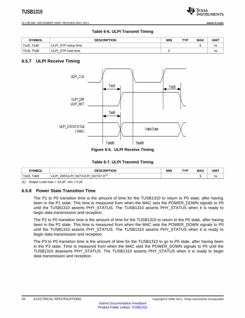
Table 6-6. ULPI Transmit Timing
SYMBOL DESCRIPTION MIN TYP MAX UNIT
Tsc8, Tsd8 ULPI_STP setup time 6 ns
Thc8, Thd8 ULPI_STP hold time 0 ns
6.5.7 ULPI Receive Timing
Figure 6-5. ULPI Receive Timing
Table 6-7. ULPI Transmit Timing
SYMBOL DESCRIPTION MIN TYP MAX UNIT
Tdc9, Tdd9 ULPI_DIR/ULPI_NXT/ULPI_DATA7-0 (1) 9 ns
(1) Output Load max = 10 pF, min = 5 pF
6.5.8 Power State Transition Time
The P1 to P0 transition time is the amount of time for the TUSB1310 to return to P0 state, after havingbeen in the P1 state. This time is measured from when the MAC sets the POWER_DOWN signals to P0until the TUSB1310 asserts PHY_STATUS. The TUSB1310 asserts PHY_STATUS when it is ready tobegin data transmission and reception.
The P2 to P0 transition time is the amount of time for the TUSB1310 to return to the P0 state, after havingbeen in the P2 state. This time is measured from when the MAC sets the POWER_DOWN signals to P0until the TUSB1310 asserts PHY_STATUS. The TUSB1310 asserts PHY_STATUS when it is ready tobegin data transmission and reception.
The P3 to P0 transition time is the amount of time for the TUSB1310 to go to P0 state, after having beenin the P3 state. Time is measured from when the MAC sets the POWER_DOWN signals to P0 until theTUSB1310 deasserts PHY_STATUS. The TUSB1310 asserts PHY_STATUS when it is ready to begindata transmission and reception.
34 ELECTRICAL SPECIFICATIONS Copyright © 2009–2011, Texas Instruments Incorporated
Submit Documentation FeedbackProduct Folder Link(s): TUSB1310

PACKAGE OPTION ADDENDUM
www.ti.com 10-Dec-2020
Addendum-Page 1
PACKAGING INFORMATION
Orderable Device Status(1)
Package Type PackageDrawing
Pins PackageQty
Eco Plan(2)
Lead finish/Ball material
(6)
MSL Peak Temp(3)
Op Temp (°C) Device Marking(4/5)
Samples
TUSB1310ZAY NRND NFBGA ZAY 175 160 RoHS & Green SNAGCU Level-3-260C-168 HR 0 to 70 TUSB1310 (1) The marketing status values are defined as follows:ACTIVE: Product device recommended for new designs.LIFEBUY: TI has announced that the device will be discontinued, and a lifetime-buy period is in effect.NRND: Not recommended for new designs. Device is in production to support existing customers, but TI does not recommend using this part in a new design.PREVIEW: Device has been announced but is not in production. Samples may or may not be available.OBSOLETE: TI has discontinued the production of the device.
(2) RoHS: TI defines "RoHS" to mean semiconductor products that are compliant with the current EU RoHS requirements for all 10 RoHS substances, including the requirement that RoHS substancedo not exceed 0.1% by weight in homogeneous materials. Where designed to be soldered at high temperatures, "RoHS" products are suitable for use in specified lead-free processes. TI mayreference these types of products as "Pb-Free".RoHS Exempt: TI defines "RoHS Exempt" to mean products that contain lead but are compliant with EU RoHS pursuant to a specific EU RoHS exemption.Green: TI defines "Green" to mean the content of Chlorine (Cl) and Bromine (Br) based flame retardants meet JS709B low halogen requirements of <=1000ppm threshold. Antimony trioxide basedflame retardants must also meet the <=1000ppm threshold requirement.
(3) MSL, Peak Temp. - The Moisture Sensitivity Level rating according to the JEDEC industry standard classifications, and peak solder temperature.
(4) There may be additional marking, which relates to the logo, the lot trace code information, or the environmental category on the device.
(5) Multiple Device Markings will be inside parentheses. Only one Device Marking contained in parentheses and separated by a "~" will appear on a device. If a line is indented then it is a continuationof the previous line and the two combined represent the entire Device Marking for that device.
(6) Lead finish/Ball material - Orderable Devices may have multiple material finish options. Finish options are separated by a vertical ruled line. Lead finish/Ball material values may wrap to twolines if the finish value exceeds the maximum column width.
Important Information and Disclaimer:The information provided on this page represents TI's knowledge and belief as of the date that it is provided. TI bases its knowledge and belief on informationprovided by third parties, and makes no representation or warranty as to the accuracy of such information. Efforts are underway to better integrate information from third parties. TI has taken andcontinues to take reasonable steps to provide representative and accurate information but may not have conducted destructive testing or chemical analysis on incoming materials and chemicals.TI and TI suppliers consider certain information to be proprietary, and thus CAS numbers and other limited information may not be available for release.
In no event shall TI's liability arising out of such information exceed the total purchase price of the TI part(s) at issue in this document sold by TI to Customer on an annual basis.

TRAY
Chamfer on Tray corner indicates Pin 1 orientation of packed units.
*All dimensions are nominal
Device PackageName
PackageType
Pins SPQ Unit arraymatrix
Maxtemperature
(°C)
L (mm) W(mm)
K0(µm)
P1(mm)
CL(mm)
CW(mm)
TUSB1310ZAY ZAY NFBGA 175 160 8 x 20 150 315 135.9 7620 15.4 11.2 19.65
PACKAGE MATERIALS INFORMATION
www.ti.com 5-Jan-2022
Pack Materials-Page 1

www.ti.com
PACKAGE OUTLINE
12.111.9
12.111.9
1.4 MAX
0.450.35
175X 0.550.45
10.4 TYP
10.4 TYP
0.8 TYP
0.8 TYP
(0.8)
(0.8)
NFBGA - 1.4 mm max heightZAY0175APLASTIC BALL GRID ARRAY
4219814/A 05/2020
NOTES: 1. All linear dimensions are in millimeters. Any dimensions in parenthesis are for reference only. Dimensioning and tolerancing per ASME Y14.5M. 2. This drawing is subject to change without notice.
BALL A1CORNER
⌓ 0.12 C
SEATING PLANE
⌖⌀0.15Ⓜ C A B⌀0.08Ⓜ C
SYMM℄
SYMM℄
1
A
2 3 4 5 6 7 8 9 10 11 12 13
B
C
D
E
F
G
H
J
K
L
M
N
14
P
SCALE 1.200
AB
C

www.ti.com
EXAMPLE BOARD LAYOUT
0.05 MAXALL AROUND
0.05 MINALL AROUND
(0.8) TYP
(0.8) TYP175X ( 0.4)
( 0.4)METAL EDGE
( 0.4)SOLDER MASKOPENING
NFBGA - 1.4 mm max heightZAY0175APLASTIC BALL GRID ARRAY
4219814/A 05/2020
NOTES: (continued) 3. Final dimensions may vary due to manufacturing tolerance considerations and also routing constraints. For information, see Texas Instruments literature number SPRAA99 (www.ti.com/lit/spraa99).
LAND PATTERN EXAMPLEEXPOSED METAL SHOWN
SCALE: 10X
SYMM℄
SYMM℄
A
1 2 3 4 5 6 7 8 9 10 11 12 13
B
C
D
E
F
G
H
J
K
L
M
N
14
P
EXPOSED METAL
SOLDER MASKOPENING
METAL UNDERSOLDER MASK
EXPOSED METAL
SOLDER MASK DETAILSNOT TO SCALE
NON-SOLDER MASKDEFINED
(PREFERRED)
SOLDER MASKDEFINED

www.ti.com
EXAMPLE STENCIL DESIGN
(0.8) TYP
(0.8) TYP
175X ( 0.4)
NFBGA - 1.4 mm max heightZAY0175APLASTIC BALL GRID ARRAY
4219814/A 05/2020
NOTES: (continued) 4. Laser cutting apertures with trapezoidal walls and rounded corners may offer better paste release.
SOLDER PASTE EXAMPLEBASED ON 0.125 mm THICK STENCIL
SCALE: 10X
SYMM℄
SYMM℄
A
1 2 3 4 5 6 7 8 9 10 11 12 13
B
C
D
E
F
G
H
J
K
L
M
N
14
P

IMPORTANT NOTICE AND DISCLAIMERTI PROVIDES TECHNICAL AND RELIABILITY DATA (INCLUDING DATA SHEETS), DESIGN RESOURCES (INCLUDING REFERENCE DESIGNS), APPLICATION OR OTHER DESIGN ADVICE, WEB TOOLS, SAFETY INFORMATION, AND OTHER RESOURCES “AS IS” AND WITH ALL FAULTS, AND DISCLAIMS ALL WARRANTIES, EXPRESS AND IMPLIED, INCLUDING WITHOUT LIMITATION ANY IMPLIED WARRANTIES OF MERCHANTABILITY, FITNESS FOR A PARTICULAR PURPOSE OR NON-INFRINGEMENT OF THIRD PARTY INTELLECTUAL PROPERTY RIGHTS.These resources are intended for skilled developers designing with TI products. You are solely responsible for (1) selecting the appropriate TI products for your application, (2) designing, validating and testing your application, and (3) ensuring your application meets applicable standards, and any other safety, security, regulatory or other requirements.These resources are subject to change without notice. TI grants you permission to use these resources only for development of an application that uses the TI products described in the resource. Other reproduction and display of these resources is prohibited. No license is granted to any other TI intellectual property right or to any third party intellectual property right. TI disclaims responsibility for, and you will fully indemnify TI and its representatives against, any claims, damages, costs, losses, and liabilities arising out of your use of these resources.TI’s products are provided subject to TI’s Terms of Sale or other applicable terms available either on ti.com or provided in conjunction with such TI products. TI’s provision of these resources does not expand or otherwise alter TI’s applicable warranties or warranty disclaimers for TI products.TI objects to and rejects any additional or different terms you may have proposed. IMPORTANT NOTICE
Mailing Address: Texas Instruments, Post Office Box 655303, Dallas, Texas 75265Copyright © 2022, Texas Instruments Incorporated