model usb-dio-48 usb 48 channel digital input/output module ...
Upload
khangminh22Category
view
1download
0
Power Integrations
5245 Hellyer Avenue, San Jose, CA 95138 USA. Tel: +1 408 414 9200 Fax: +1 408 414 9201
www.power.com
Design Example Report
Title
100 W USB PD 3.0 Power Supply w ith 3.3 V – 21 V / 5 A (100 W Power-limited) PPS Output Using InnoSw itchTM3-PD Pow iGaNTM INN3870C-H805 and HiperPFS-4 PFS7628C
Specification
90 VAC – 265 VAC Input; 5 V / 5 A, 9 V / 5 A, 12 V / 5 A, 15 V / 5 A, 20 V / 5 A, or 3.3 V – 21 V / 5 A PPS (100 W Power-limited) Output
Application USB PD / PPS Power Adapter
Author Applications Engineering Department
Document Number DER-937
Date October 18, 2021
Revision 1.0 Summary and Features • InnoSwitch3-PD: Off-Line CV/CC QR flyback switcher IC with integrated USB Type-C and USB-PD
controller, integrated high-voltage switch, synchronous rectification and FluxLinkTM feedback o Integrated USB Type-C and USB-PD controller reduces footprint, no external controller required o Comprehensive protection features with telemetry for power supply status and fault monitoring
• Meets DOE6 and CoC v5 2016 Average Efficiency requirements with at least 2.0% pass margin o 5 V Output: 92.10% at 115 VAC (7.11% margin); 91.47% at 230 VAC (6.48% margin) o 9 V Output: 92.60% at 115 VAC (3.75% margin); 92.77% at 230 VAC (3.91% margin) o 12 V Output: 92.64% at 115 VAC (3.64% margin); 93.17% at 230 VAC (4.17% margin) o 15 V Output: 91.87% at 115 VAC (2.87% margin); 91.97% at 230 VAC (2.97% margin) o 20 V Output: 91.30% at 115 VAC (2.20% margin); 91.32% at 230 VAC (2.32% margin)
• Meets CoC v5 2016 10% Load Efficiency requirements with high margin (>9.0%) for all PDOs • <40 mW no-load input power at 230 VAC • Meets CISPR22 / EN55022 Class B conducted EMI with high margin
o >6dB margin at worst case condition (20 V / 5 A, 115 VAC) • High power density: 15.0 W / inch3 without enclosure (3.30” x 2.17” x 0.93” form factor) • Low component count: 121 total

DER-937 100 W InnoSwitch3-PD USB PD 3.0 with PPS 18-Oct-21
Page 2 of 131
Power Integrations, Inc. Tel: +1 408 414 9200 Fax: +1 408 414 9201 www.power.com
PATENT INFORMATION The products and applications illustrated herein (including transformer construction and circuits external to the products) may be covered by one or more U.S. and foreign patents, or potentially by pending U.S. and foreign patent applications assigned to Power Integrations. A complete list of Power Integrations' patents may be found at www.power.com. Power Integrations grants its customers a license under certain patent rights as set forth at https://www.power.com/company/intellectual-property-licensing/.

DER-937 100 W InnoSwitch3-PD USB PD 3.0 with PPS 18-Oct-21
Page 3 of 131
Power Integrations, Inc. Tel: +1 408 414 9200 Fax: +1 408 414 9201 www.power.com
Table of Contents 1 Introduction ....................................................................................................... 7 2 Power Supply Specification .................................................................................. 9 3 Schematic ........................................................................................................ 11 4 Circuit Description ............................................................................................ 13
4.1 Input Rectifier and EMI Filter ...................................................................... 13 4.2 HiperPFS-4 PFS7628C PFC Boost Converter ................................................. 13
PFC Input Line Feed-Forward Sense Circuit ........................................... 13 PFC Output Feedback Circuit ................................................................ 13 Bias Supply with Hysteresis Control to HiperPFS-4 IC ............................. 14
4.3 InnoSwitch3-PD IC Primary ........................................................................ 15 4.4 InnoSwitch3-PD IC Secondary and USB Power Delivery Controller ................. 16
5 PCB Layout ...................................................................................................... 18 6 Bill of Materials ................................................................................................ 19 7 Common Mode Choke Specifications (L1) ........................................................... 21
7.1 Electrical Diagram ...................................................................................... 21 7.2 Electrical Specifications .............................................................................. 21 7.3 Material List .............................................................................................. 21 7.4 Winding Instructions .................................................................................. 21
8 PFC Inductor Specification (L4) ......................................................................... 22 8.1 Electrical Diagram ...................................................................................... 22 8.2 Electrical Specifications .............................................................................. 22 8.3 Inductor Build Diagram .............................................................................. 22 8.4 Material List .............................................................................................. 23 8.5 Winding Instructions .................................................................................. 23
9 Transformer Specification (T1) .......................................................................... 25 9.1 Electrical Diagram ...................................................................................... 25 9.2 Electrical Specifications .............................................................................. 25 9.3 Transformer Build Diagram ......................................................................... 26 9.4 Material List .............................................................................................. 26 9.5 Winding Instructions .................................................................................. 27
10 PFC Inductor Design Spreadsheet .................................................................. 35 11 Transformer Design Spreadsheet ................................................................... 40
11.1 Flyback Stage with PFC ON ......................................................................... 40 11.2 Flyback Stage with PFC OFF ....................................................................... 44
12 Performance Data ......................................................................................... 48 12.1 No-Load Input Power ................................................................................. 48 12.2 Full Load Efficiency (On-board) ................................................................... 49 12.3 Average and 10% Load Efficiency ............................................................... 49
Efficiency Requirements ....................................................................... 49 Efficiency Performance Summary (On Board) ........................................ 49 Average and 10% Load Efficiency Measurements................................... 50
12.4 Efficiency Across Line at 100% Load (On Board) .......................................... 53 12.5 Efficiency Across Load (On Board) ............................................................... 54

DER-937 100 W InnoSwitch3-PD USB PD 3.0 with PPS 18-Oct-21
Page 4 of 131
Power Integrations, Inc. Tel: +1 408 414 9200 Fax: +1 408 414 9201 www.power.com
Output: 5 V / 5 A ................................................................................ 54 Output: 9 V / 5 A ................................................................................ 55 Output: 12 V / 5 A .............................................................................. 56 Output: 15 V / 5 A .............................................................................. 57 Output: 20 V / 5 A .............................................................................. 61
12.6 Load Regulation (On Board) ....................................................................... 65 Output: 5 V / 5 A ................................................................................ 65 Output: 9 V / 5 A ................................................................................ 66 Output: 12 V / 5 A .............................................................................. 67 Output: 15 V / 5 A .............................................................................. 68 Output: 20 V / 5 A .............................................................................. 69
12.7 Line Regulation (On Board) ........................................................................ 70 Output: 5 V / 5 A ................................................................................ 70 Output: 9 V / 5 A ................................................................................ 71 Output: 12 V / 5 A .............................................................................. 72 Output: 15 V / 5 A .............................................................................. 73 Output: 20 V / 5 A .............................................................................. 74
12.8 Input Current Harmonics ............................................................................ 75 Output: 15 V / 5 A (115 VAC) ............................................................... 75 Output: 15 V / 5 A (230 VAC) ............................................................... 77 Output: 20 V / 5 A (115 VAC) ............................................................... 79 Output: 20 V / 5 A (230 VAC) ............................................................... 81
13 Thermal Performance .................................................................................... 83 13.1 Thermal Performance in Open Case, Room Temperature .............................. 83
Output: 5 V / 5 A (90 VAC) .................................................................. 83 Output: 5 V / 5 A (265 VAC) ................................................................ 84 Output: 9 V / 5 A (90 VAC) .................................................................. 85 Output: 9 V / 5 A (265 VAC) ................................................................ 85 Output: 12 V / 5 A (90 VAC) ................................................................ 86 Output: 12 V / 5 A (265 VAC) ............................................................... 86 Output: 15 V / 5 A (90 VAC) ................................................................ 87 Output: 15 V / 5 A (265 VAC) ............................................................... 87 Output: 20 V / 5 A (90 VAC) ................................................................ 88
Output: 20 V / 5 A (265 VAC) ........................................................... 88 14 Waveforms ................................................................................................... 89
14.1 Input Voltage and Current Waveforms ......................................................... 89 Output: 15 V / 5 A .............................................................................. 89 Output: 20 V / 5 A .............................................................................. 89
14.2 PFC Inductor Current and HiperPFS-4 Drain Voltage Waveforms .................... 90 Output: 15 V / 5 A .............................................................................. 90 Output: 20 V / 5 A .............................................................................. 90
14.3 Start-up Waveforms ................................................................................... 91 Output Voltage and Current ................................................................. 91 Primary Drain Voltage and Current ....................................................... 92 SR FET Drain Voltage and Current ........................................................ 92

DER-937 100 W InnoSwitch3-PD USB PD 3.0 with PPS 18-Oct-21
Page 5 of 131
Power Integrations, Inc. Tel: +1 408 414 9200 Fax: +1 408 414 9201 www.power.com
14.4 Primary Drain Voltage and Current (Steady-State) ........................................ 93 Output: 5 V / 5 A ................................................................................ 93 Output: 9 V / 5 A ................................................................................ 93 Output: 12 V / 5 A .............................................................................. 94 Output: 15 V / 5 A .............................................................................. 94 Output: 20 V / 5 A .............................................................................. 95
14.5 SR FET Drain Voltage and Current (Steady-State) ......................................... 96 Output: 5 V / 5 A ................................................................................ 96 Output: 9 V / 5 A ................................................................................ 96 Output: 12 V / 5 A .............................................................................. 97 Output: 15 V / 5 A .............................................................................. 97 Output: 20 V / 5 A .............................................................................. 98
14.6 Primary and SR FET Drain Voltage and Current (during Output Voltage Transition) .......................................................................................................... 99
Primary Drain Voltage and Current, 3.3 V to 21 V PPS Transition ............ 99 SR FET Drain Voltage and Current, 3.3 V to 21 V Transition ...................100
14.7 Load Transient Response ..........................................................................101 Output: 5 V / 5 A ...............................................................................101 Output: 9 V / 5 A ...............................................................................102 Output: 12 V / 5 A .............................................................................102 Output: 15 V / 5 A .............................................................................103 Output: 20 V / 5 A .............................................................................103
14.8 Output Ripple Measurements .....................................................................104 Ripple Measurement Technique ...........................................................104 Output Voltage Ripple Waveforms .......................................................105 Output Voltage Ripple Amplitude vs. Load ............................................108
15 CV/CC Profile ...............................................................................................113 15.1 Output: 20 V / 5 A PPS Request, PDO6 (100 W Power-Limited) ....................113 15.2 Output: 21 V / 5 A PPS Request, PDO6 (100 W Power-Limited) ....................114
16 Voltage Step and Current Limit Test using QuadraMAX and Total Phase Analyzer 115
16.1 Voltage Step Test (VST) ............................................................................115 16.2 Current Limit Test (CLT) ............................................................................116
17 Conducted EMI ............................................................................................117 17.1 Floating Ground (QPK / AV) .......................................................................117
Output: 5 V / 5 A ...............................................................................117 Output: 9 V / 5 A ...............................................................................118 Output: 12 V / 5 A .............................................................................119 Output: 15 V / 5 A .............................................................................120 Output: 20 V / 5 A .............................................................................121
18 Combination Wave Surge .............................................................................122 18.1 Differential Mode Surge (L1 to L2), 230 VAC Input ......................................122 18.2 Common Mode Surge (L1, L2 to PE), 230 VAC Input ....................................122 18.3 Common Mode Surge (L1 to PE), 230 VAC Input .........................................122 18.4 Common Mode Surge (L2 to PE), 230 VAC Input .........................................123

DER-937 100 W InnoSwitch3-PD USB PD 3.0 with PPS 18-Oct-21
Page 6 of 131
Power Integrations, Inc. Tel: +1 408 414 9200 Fax: +1 408 414 9201 www.power.com
19 Electrostatic Discharge .................................................................................124 19.1 VOUT and GND ESD Performance ..............................................................124
Air Discharge, End of Cable, 230 VAC Input ..........................................125 Air Discharge, On-board, 230 VAC Input ..............................................126 Contact Discharge, End of Cable, 230 VAC Input ..................................127 Contact Discharge, On the Board, 230 VAC Input ..................................127
19.2 CC1 and CC2 ESD Performance ..................................................................128 Air Discharge, End of cable, 230 VAC Input ..........................................129 Contact Discharge, End of Cable, 230 VAC Input ..................................129
20 Revision History ...........................................................................................130 Important Note: Although this board is designed to satisfy safety isolation requirements, the engineering prototype has not been agency approved. Therefore, all testing should be performed using an isolation transformer to provide the AC input to the prototype board.
DER-937 100 W InnoSwitch3-PD USB PD 3.0 with PPS 18-Oct-21
Page 7 of 131
Power Integrations, Inc. Tel: +1 408 414 9200 Fax: +1 408 414 9201 www.power.com
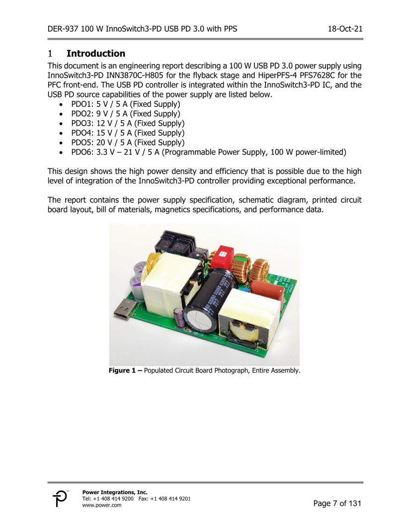
Introduction This document is an engineering report describing a 100 W USB PD 3.0 power supply using InnoSwitch3-PD INN3870C-H805 for the flyback stage and HiperPFS-4 PFS7628C for the PFC front-end. The USB PD controller is integrated within the InnoSwitch3-PD IC, and the USB PD source capabilities of the power supply are listed below.
• PDO1: 5 V / 5 A (Fixed Supply) • PDO2: 9 V / 5 A (Fixed Supply) • PDO3: 12 V / 5 A (Fixed Supply) • PDO4: 15 V / 5 A (Fixed Supply) • PDO5: 20 V / 5 A (Fixed Supply) • PDO6: 3.3 V – 21 V / 5 A (Programmable Power Supply, 100 W power-limited)
This design shows the high power density and efficiency that is possible due to the high level of integration of the InnoSwitch3-PD controller providing exceptional performance. The report contains the power supply specification, schematic diagram, printed circuit board layout, bill of materials, magnetics specifications, and performance data.
Figure 1 – Populated Circuit Board Photograph, Entire Assembly.
DER-937 100 W InnoSwitch3-PD USB PD 3.0 with PPS 18-Oct-21
Page 8 of 131
Power Integrations, Inc. Tel: +1 408 414 9200 Fax: +1 408 414 9201 www.power.com
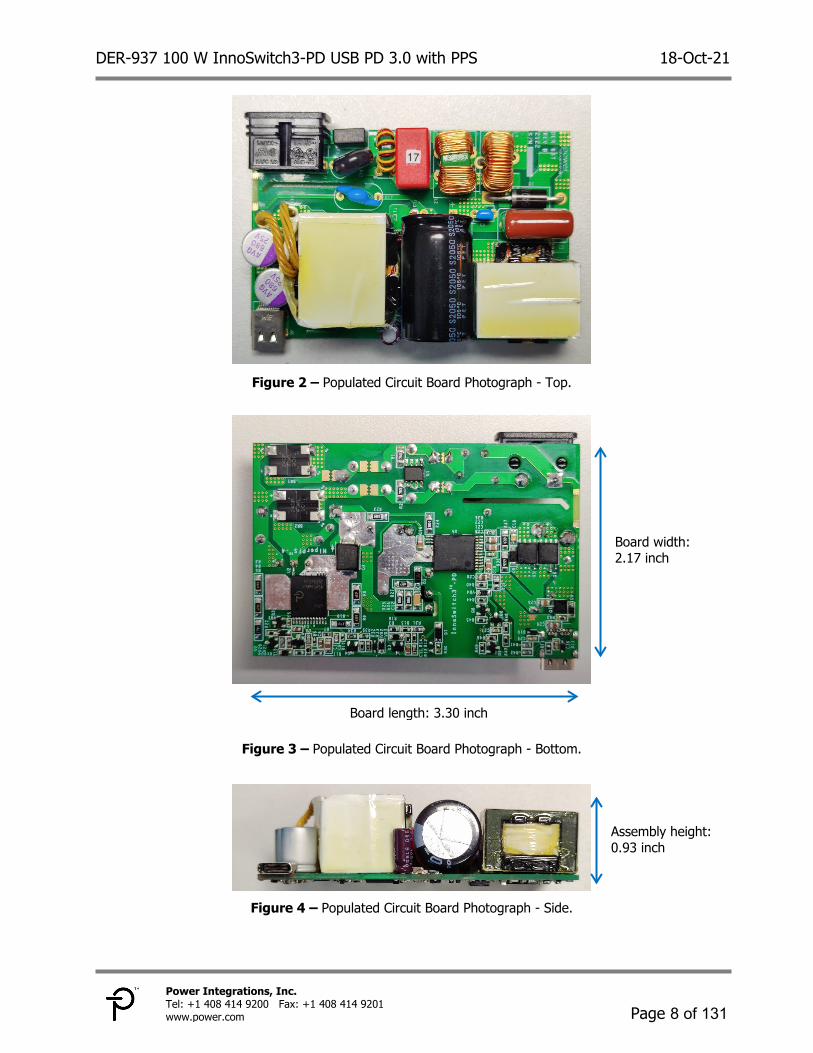
Figure 2 – Populated Circuit Board Photograph - Top.
Figure 3 – Populated Circuit Board Photograph - Bottom.
Figure 4 – Populated Circuit Board Photograph - Side.
Assembly height: 0.93 inch
Board width: 2.17 inch
Board length: 3.30 inch

DER-937 100 W InnoSwitch3-PD USB PD 3.0 with PPS 18-Oct-21
Page 9 of 131
Power Integrations, Inc. Tel: +1 408 414 9200 Fax: +1 408 414 9201 www.power.com
Power Supply Specification The table below represents the minimum acceptable performance of the design. Actual performance is listed in the results section.
Description Symbol Min Typ Max Units Comment Input Input Voltage VIN 90 265 VAC 2 Wire – no P.E. Input Frequency fLINE 47 50/60 64 Hz No-load Input Power 40 mW Measured at 230 VAC USB PD 3.0 Output: Fixed Supply PDOs 5 V / 5 A Fixed Supply PDO1
Output Voltage VOUT(5 V) 5.0 V See Note A. Output Voltage Ripple VRIPPLE(5 V) 125 mV Measured at End of 100 mΩ Cable. See Note B. Output Current IOUT(5 V) 5.0 A See Note C.
Average Efficiency ƞ(5 V) 91.6 % Average Efficiency at 115 VAC with VOUT Measured on the Board.
Continuous Output Power POUT(5 V) 25 W 9 V / 5 A Fixed Supply PDO2
Output Voltage VOUT(9 V) 9.0 V See Note A. Output Voltage Ripple VRIPPLE(9 V) 125 mV Measured at End of 100 mΩ Cable. See Note B. Output Current IOUT(9 V) 5.0 A See Note C.
Average Efficiency ƞ(9 V) 92.1 % Average Efficiency at 115 VAC with VOUT Measured on the Board.
Continuous Output Power POUT(9 V) 45 W 12 V / 5 A Fixed Supply PDO3
Output Voltage VOUT(12 V) 12.0 V See Note A. Output Voltage Ripple VRIPPLE(12 V) 125 mV Measured at End of 100 mΩ Cable. See Note B. Output Current IOUT(12 V) 5.0 A See Note C.
Average Efficiency ƞ(12 V) 92.1 % Average Efficiency at 115 VAC with VOUT Measured on the Board.
Continuous Output Power POUT(12 V) 60 W 15 V / 5 A Fixed Supply PDO4
Output Voltage VOUT(15 V) 15.0 V See Note A. Output Voltage Ripple VRIPPLE(15 V) 125 mV Measured at End of 100 mΩ Cable. See Note B. Output Current IOUT(15 V) 5.0 A See Note C.
Average Efficiency ƞ(15 V) 91.3 % Average Efficiency at 115 VAC with VOUT Measured on the Board.
Continuous Output Power POUT(15 V) 75 W 20 V / 5 A Fixed Supply PDO5
Output Voltage VOUT(20 V) 20.0 V See Note A. Output Voltage Ripple VRIPPLE(20 V) 125 mV Measured at End of 100 mΩ Cable. See Note B. Output Current IOUT(20 V) 5.0 A See Note C.
Average Efficiency ƞ(20 V) 90.8 % Average Efficiency at 115 VAC with VOUT Measured on the Board.
Continuous Output Power POUT(20 V) 100 W

DER-937 100 W InnoSwitch3-PD USB PD 3.0 with PPS 18-Oct-21
Page 10 of 131
Power Integrations, Inc. Tel: +1 408 414 9200 Fax: +1 408 414 9201 www.power.com
Description Symbol Min Typ Max Units Comment USB PD 3.0 Output: Programmable Power Supply APDOs 3.3 V – 21 V / 5 A PPS APDO6
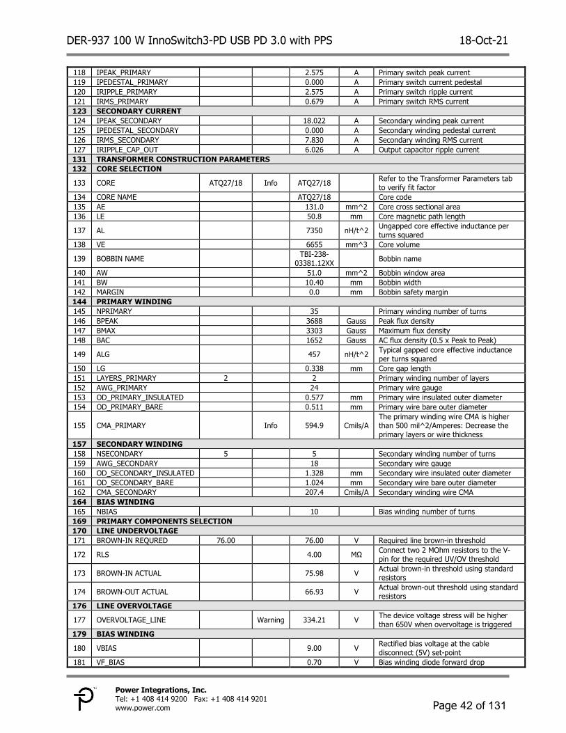
Programmable Output Voltage Range VOUT(PDO6) 3.3 21 V APDO Minimum and Maximum Voltage.
See Note A.
Programmable Output Current Limit Range IOUT(PDO6) 1.0 5.0 A See Note D.
PPS Voltage Step VSTEP(PDO6) 20 mV PPS Voltage Step (USB PD 3.0). PPS Current Step ISTEP(PDO6) 50 mA PPS Current Step (USB PD 3.0).
Continuous Output Power POUT(PDO6) 100 W PPS Power Limited bit = 1 (USB PD 3.0). See Note E.
Conducted EMI Margin 6 dB Meets CISPR22B / EN55022B Ambient Temperature TAMB 0 45 ºC Open Frame, Sea Level. Note A: Output Voltage Regulation compliant with USB PD 3.0 Specifications.
B: Output Voltage Ripple measured at the end of 100 mΩ cable with the probe having decoupling capacitors 47 uF electrolytic and 100 nF ceramic in parallel. C: Maximum Operating Current for the Fixed Supply PDO. Output Over Current Protection Threshold nominally set at 250 mA above the Operating Current requested by the USB PD Sink. D: Output Current Limit Accuracy is within ±150 mA for Operating Current between 1 A and 3 A, or ±5% for Operating Current > 3 A; compliant with USB PD 3.0 Specifications. E: For PPS APDOs with Power Limited bit set to 1, whenever the USB PD Sink sends a valid Output
Voltage and Current Limit request that exceeds 100 W, the power supply will provide the requested output voltage and an output current limit that matches 100 W maximum output power. Note: To use this design for a charger/adapter with a different shape and form factor, the changes in the circuit board layout must be carefully evaluated to meet the target specifications for EMI, ESD, and Line Surge performance.
DER-937 100 W InnoSwitch3-PD USB PD 3.0 with PPS 18-Oct-21
Page 11 of 131
Power Integrations, Inc. Tel: +1 408 414 9200 Fax: +1 408 414 9201 www.power.com
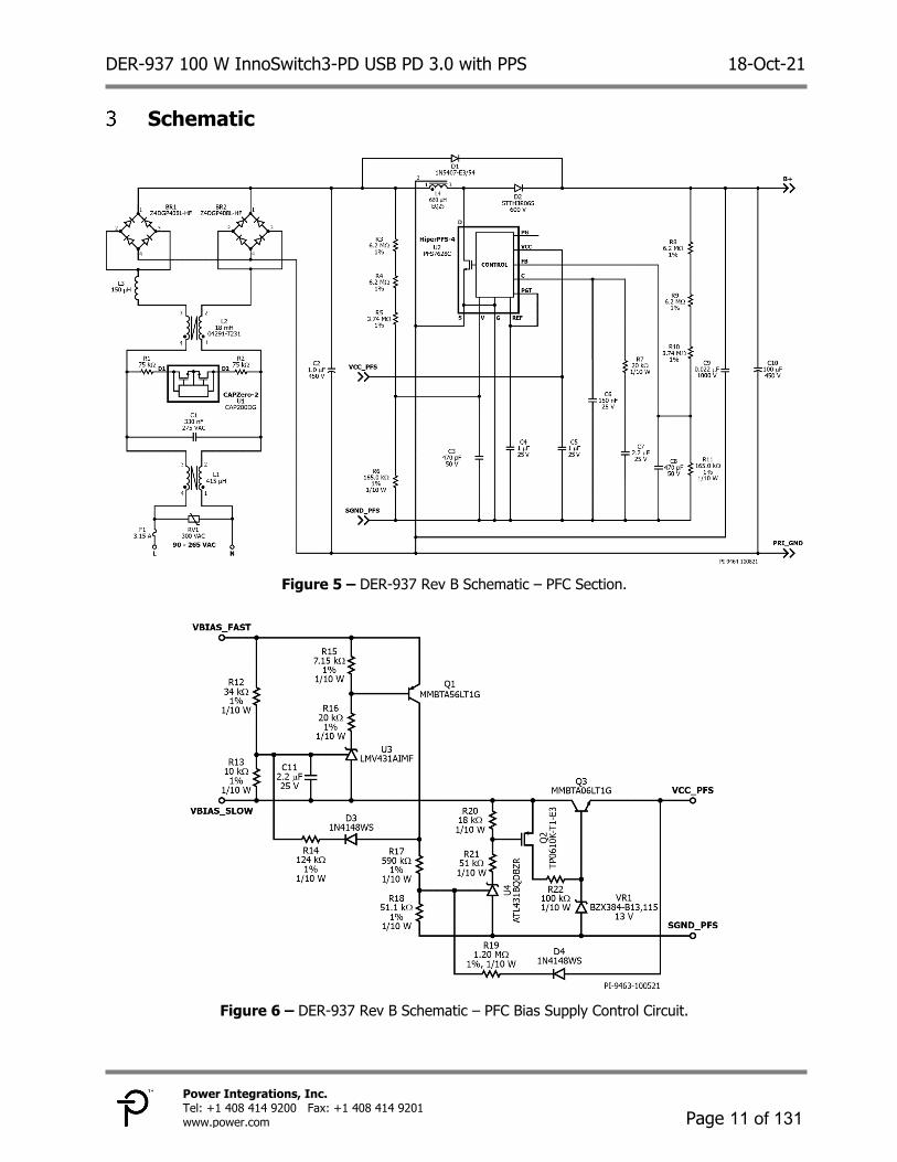
Schematic
Figure 5 – DER-937 Rev B Schematic – PFC Section.
Figure 6 – DER-937 Rev B Schematic – PFC Bias Supply Control Circuit.

DER-937 100 W InnoSwitch3-PD USB PD 3.0 with PPS 18-Oct-21
Page 12 of 131
Power Integrations, Inc. Tel: +1 408 414 9200 Fax: +1 408 414 9201 www.power.com
Figure 7 – DER-937 Rev B Schematic – Flyback Section.
DER-937 100 W InnoSwitch3-PD USB PD 3.0 with PPS 18-Oct-21
Page 13 of 131
Power Integrations, Inc. Tel: +1 408 414 9200 Fax: +1 408 414 9201 www.power.com
Circuit Description
Input Rectifier and EMI Filter The input fuse F1 isolates the circuit and provides protection from component failure. Metal oxide varistor RV1 offers protection during line surge events by effectively clamping the input voltage seen by the power supply. Common mode chokes L1 and L2, differential mode choke L3, along with capacitors C17, C1, and C2 provide common mode and differential mode noise filtering for EMI attenuation. Bridge rectifiers BR1 and BR2 rectifies the AC line voltage to have a full wave rectified DC. The CAPZero-2 IC U1 with resistors R1 and R2 discharge the stored energy in capacitor C1 when the power supply is disconnected from AC mains. The CAPZero-2 IC eliminates static losses in R1 and R2 by only connecting these components across C1 when AC input is removed.
HiperPFS-4 PFS7628C PFC Boost Converter The PFC boost converter power stage consists of the HiperPFS-4 IC U2, boost inductor L4, ultrafast diode D2, and output filter capacitor C10. With an active PFC boost converter as a front-end stage of the power supply, a sinusoidal input current with low harmonic content is maintained while having a regulated DC voltage to the flyback DC-DC converter stage of the power supply. Diode D1 acts as a pre-charge diode, preventing a resonant build-up of output voltage during start-up by bypassing L4 while simultaneously charging C10. Capacitor C9 provides a short, high-frequency return path from PFC output B+ to primary ground RTN for improved EMI performance and reduce voltage overshoot across the MOSFET drain-source inside U2 at each turn-off edge. HiperPFS-4 IC U2 is configured in full power mode by capacitor C4 which is connected to the REF pin.
PFC Input Line Feed-Forward Sense Circuit The rectified DC voltage at the PFC input is sensed by HiperPFS-4 IC U2 using resistors R3-R6. These resistors have large values to minimize power consumption. The resistor values are also matched with the FEEDBACK pin resistor divider network for optimized power factor performance. Capacitor C3 filters noise coupled into the VOLTAGE MONITOR pin.
PFC Output Feedback Circuit Output voltage divider network comprising of resistors R8-R11 are used to scale the output voltage and provide feedback to the IC. The resistor values are set to have a PFC output voltage of 380 V. Capacitor C8 filters noise coupled into the FEEDBACK pin.

DER-937 100 W InnoSwitch3-PD USB PD 3.0 with PPS 18-Oct-21
Page 14 of 131
Power Integrations, Inc. Tel: +1 408 414 9200 Fax: +1 408 414 9201 www.power.com
Components R7, C6, and C7 are required for shaping the loop response of the feedback network.
Bias Supply with Hysteresis Control to HiperPFS-4 IC The HiperPFS-4 IC requires a regulated VCC supply of 12 V nominal for normal operation, with an absolute maximum voltage of 15 V. Capacitor C5 provides noise filtering to the VCC pin. Bringing the VCC pin voltage below the shutdown VCC voltage threshold will trigger an undervoltage lock-out protection and disable switching of the HiperPFS-4 device. The PFC bias supply is derived from the flyback stage auxiliary output as shown previously in Figure 8. From a single bias winding, two rectified and filtered voltages are created: (1) VBIAS_Fast generated using US1DWF-7 ultrafast recovery diode D6, RC snubber R28 and C13, series resistor R29, filter capacitor C14, and shunt resistor R31; and (2) VBIAS_Slow generated using S1MLHRVG standard recovery diode D7, series resistor R30, and filter capacitor C15. Any of the two voltages, VBIAS_Fast and VBIAS_Slow, can be used to estimate the flyback converter output voltage. Moreover, the voltage difference between VBIAS_Fast and VBIAS_Slow provide a signal which increases as flyback output current increases. Therefore, this voltage difference, VBIAS_delta, can also be used to estimate the flyback converter output current. The HiperPFS-4 VCC pin voltage is controlled such that the PFC stage is operational when the power supply input power is 75 W or higher, and the PFC stage is disabled when the load current is equal to or less than 10% of rated IOUT. This control scheme results in significantly high efficiency at light load (10% and below) for all supported output voltage settings as compared to when both PFC stage and flyback stage are operational. The PFC bias supply circuit monitors VBIAS_Fast and VBIAS_Slow as previously shown in Figure 6. The first stage consists of the following: LMV431 IC U3 functions as a comparator, resistor divider R12 and R13 sets turn on threshold of U3, capacitor C11 filters the input terminal of U3, resistors R15 and R16 provide bias to PNP BJT Q1 when comparator U3 turns on, and diode D3 and resistor R14 provide hysteresis. Whenever VBIAS_delta (estimate of output current) exceeds 5.25 V typical, Q1 will turn on and VBIAS_Fast (estimate of output voltage) will be monitored by the second stage of the PFC bias supply circuit. VBIAS_delta turn off threshold of 4.65 V typical is set using D3 and R14 to prevent turn on/off chatter. Similarly, the PFC bias circuit second stage consists of the following: ATL431 IC U4 functions as a comparator, resistor divider R17 and R18 sets turn on threshold of U4, resistors R20 and R21 provide bias to P-channel MOSFET Q2, diode D4 and resistor R19 provide hysteresis, and a linear regulator formed by resistor R22, Zener diode VR1, and NPN transistor Q3 provides either 12.4 V or 0 V to the HiperPFS-4 IC VCC pin depending on Q2 state. Whenever the first stage is at on-state (output current exceeds threshold) and VBIAS_Fast exceeds 31.4 V typical, Q2 will turn on and effectively enable the PFC

DER-937 100 W InnoSwitch3-PD USB PD 3.0 with PPS 18-Oct-21
Page 15 of 131
Power Integrations, Inc. Tel: +1 408 414 9200 Fax: +1 408 414 9201 www.power.com
stage of the power supply. VBIAS_Fast turn off threshold of 26.4 V typical is set with D4 and R19 to prevent turn on/off chatter. The PFC bias supply circuit uses VBIAS_Fast and VBIAS_Slow signals in the flyback primary-side as indirect estimates of output voltage and current in the flyback secondary-side. The corresponding flyback output voltage and current at which the PFC turns on varies with AC input voltage because the peak-charging of the fast bias filter capacitor C14 differs from low-line to high-line. When operating at a fixed output voltage, the output current threshold for PFC turn-off is practically independent on AC input voltage since the flyback stage will be operating at 380 VDC input. Slight changes in PFC turn on/off thresholds is also expected across a wide operating ambient temperature or when the effective transformer leakage inductance is changed (for example, inserting a wire loop on the secondary-side for current probe to measure SR FET drain current waveform). The bias diode reverse recovery values, RC snubber values, resistance ratios and values, and amount of hysteresis have been tuned in this power supply such that the variations mentioned above are reduced. The resulting performance data are presented in Section 12 of this document.
InnoSw itch3-PD IC Primary One end of the flyback transformer T1 primary winding is connected to the PFC stage output capacitor and the other end is connected to the drain terminal of the switch inside the InnoSwitch3-PD IC U5. Resistors R23 and R24 provide input voltage sensing for protection in case of AC input undervoltage or overvoltage. A low-cost RCD clamp formed by diode D5, resistors R25, R26, and R27, and capacitor C12 limits the peak drain-source voltage of U5 at the instant the switch inside U5 turns off. The clamp helps to dissipate the energy stored in the leakage reactance of transformer T1. The IC is self-starting, using an internal high-voltage current source to charge the BPP pin capacitor C16 when AC is first applied. During normal operation, the primary side block is powered from an auxiliary winding on the transformer T1. VBIAS_Slow, which is the filtered supply voltage using the auxiliary winding, diode rectifier D7, series resistor R30, and filter capacitor C15, is used to power the InnoSwitch3-PD primary-side. A linear regulator comprising resistor R32, R33, BJT Q4 and Zener diode VR2 ensures sufficient current flows through R34 into the BPP pin of the InnoSwitch3-PD IC such that the internal current source of U5 is not required to charge C16 to minimize power consumption during no-load condition and at normal operation. Zener diode VR3 offers primary sensed output overvoltage protection. In a flyback converter, output of the auxiliary winding tracks the output voltage of the converter. In case of overvoltage at output of the converter, the auxiliary winding voltage increases and causes breakdown of VR3 which then causes excess current to flow into the BPP pin of InnoSwitch3-PD IC. If the current flowing into the BPP pin increases above the ISD

DER-937 100 W InnoSwitch3-PD USB PD 3.0 with PPS 18-Oct-21
Page 16 of 131
Power Integrations, Inc. Tel: +1 408 414 9200 Fax: +1 408 414 9201 www.power.com
threshold, the InnoSwitch3-PD controller will latch off and prevent any further increase in output voltage. Resistor R35 limits the current injected to BPP pin when the output overvoltage protection is triggered.
InnoSw itch3-PD IC Secondary and USB Power Delivery Controller The secondary-side of the InnoSwitch3-PD IC provides output voltage and current sensing and a gate drive to a FET for synchronous rectification. The voltage across the transformer secondary winding is rectified by the secondary-side synchronous rectifier FET (SR FET) Q5 and Q6 and filtered by capacitors C23, C24, and C25. High frequency ringing during switching transients that would otherwise create radiated EMI is reduced via a RCD snubber, R37, R38, C18, and D8. The gate of Q5 and Q6 is turned on by secondary-side controller inside IC U1, based on the secondary winding voltage sensed via resistor R36 and fed into the FWD pin of the IC. In continuous conduction mode of operation, the SR FET is turned off just prior to the secondary-side commanding a new switching cycle from the primary. In discontinuous mode of operation, the SR FET is turned off when the magnitude of the voltage drop across the SR FET falls below a threshold of approximately VSR(TH). Secondary-side control of the primary-side power switch avoids any possibility of cross conduction of the two switches and provides extremely reliable synchronous rectifier operation. The secondary-side of the IC is self-powered from either the secondary winding forward voltage or the output voltage. Capacitor C19 connected to the BPS pin of InnoSwitch3-PD IC provides decoupling for the internal circuitry. An external supply circuit from the flyback output voltage to BPS pin is formed by NPN BJT Q8, Zener diode VR4, and resistors R44 and R45. When the output voltage exceeds VR4 breakdown voltage, current is injected through this circuit to reduce the power dissipation of the regulator inside the InnoSwitch3-PD IC, effectively improving the IC temperature. The output current is sensed by monitoring the voltage drop across resistor R39. The current measurement is filtered with resistor R40 and capacitor C20, and then monitored across the IS and SECONDARY GROUND pins. An internal current sense threshold which is configured via the integrated secondary and USB PD controllers of InnoSwitch3-PD IC up to approximately 32 mV is used to reduce losses. Once the threshold is exceeded, the InnoSwitch3-PD IC uses variable frequency and variable primary switch peak current limit control schemes to maintain a fixed output current. For constant current (CC) operation, when the output voltage falls, the secondary-side controller inside InnoSwitch3-PD IC will power itself from the secondary winding directly. During the on-time of the primary-side power switch, the forward voltage that appears across the secondary winding is used to charge the SECONDARY BYPASS pin decoupling capacitor C19 via resistor R36 and an internal regulator. This allows output current
DER-937 100 W InnoSwitch3-PD USB PD 3.0 with PPS 18-Oct-21
Page 17 of 131
Power Integrations, Inc. Tel: +1 408 414 9200 Fax: +1 408 414 9201 www.power.com
regulation to be maintained down to the minimum UV threshold. Below this level the unit enters auto-restart until the output load is reduced. When the output current is below the CC threshold, the converter operates in constant voltage mode. The output voltage is monitored by the VOUT pin of the InnoSwitch3-PD IC. Similar with current regulation, the output voltage is also compared to an internal voltage threshold that is set via the integrated secondary and USB PD controllers of the InnoSwitch3-PD IC and output voltage regulation is achieved by variable frequency and variable primary switch peak current limit control schemes. Capacitor C22 is needed between the VOUT pin and the SECONDARY GROUND pin for ESD protection of the VOUT pin. N-channel MOSFET Q7 functions as the bus switch which connects or disconnects the output of the flyback converter from the USB Type-C receptacle. MOSFET Q7 is controlled by the VB/D pin on the InnoSwitch3-PD IC. Resistor R43 and diode D9 are connected across the Source and Gate terminals of the Q7 to provide a discharge path for the bus voltage when the Q7 is turned off. Capacitor C26 is used at the output for ESD protection and output voltage ripple reduction. The USB Power Delivery (USB PD) controller is integrated within the InnoSwitch3-PD IC. Capacitor C21 connected to uVCC pin serves as a decoupling capacitor. An external precision supply circuit from the flyback output voltage to uVCC pin is formed by NPN BJT Q9, shunt regulator IC U6, resistors R46-R49, and capacitor C27. Current is injected through this circuit to reduce the power dissipation of the regulator inside the InnoSwitch3-PD IC especially at high operating output voltage, effectively improving the IC temperature. When the output voltage is below approximately 4.4 V, the external circuit will not supply current into the uVCC pin and the USB PD controller will be powered through the internal regulator of the InnoSwitch3-PD IC. USB PD protocol is communicated through either CC1 or CC2 line depending on the orientation in which the Type-C plug is connected. Capacitors C29 and C30, resistors R41 and R42, and Zener diodes D10, and D11 provide protection from ESD to pins CC1 and CC2.
DER-937 100 W InnoSwitch3-PD USB PD 3.0 with PPS 18-Oct-21
Page 18 of 131
Power Integrations, Inc. Tel: +1 408 414 9200 Fax: +1 408 414 9201 www.power.com
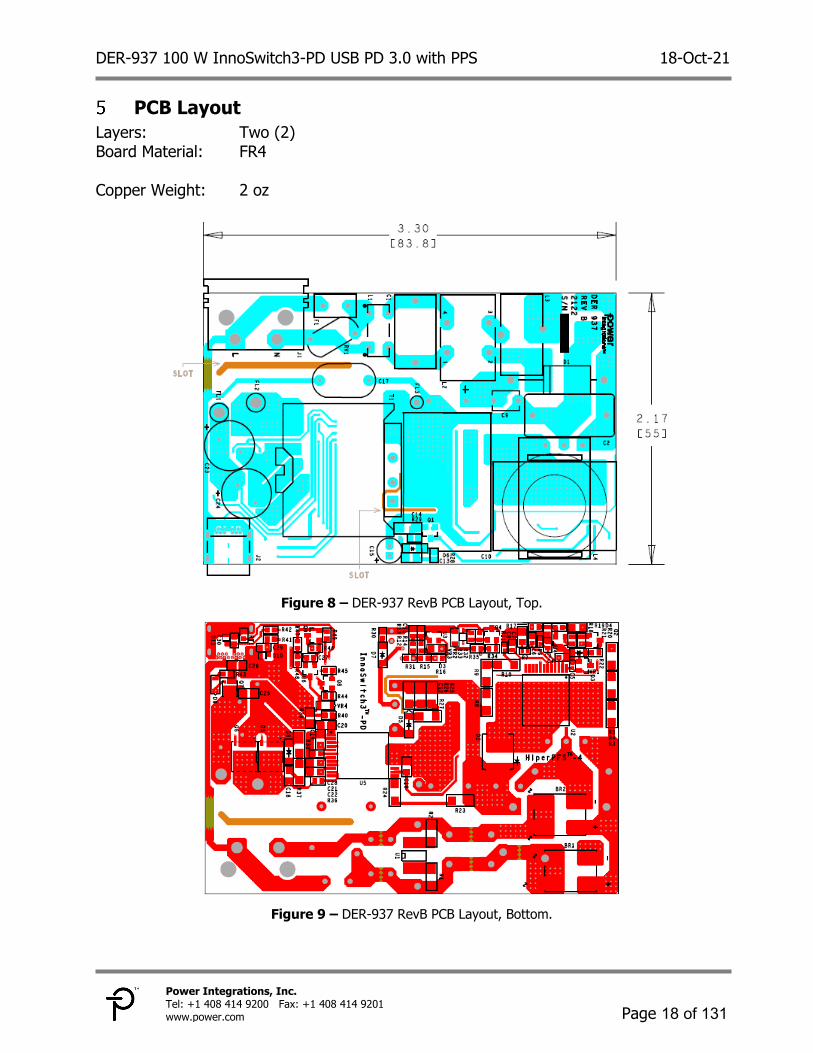
PCB Layout Layers: Two (2) Board Material: FR4
Copper Weight: 2 oz
Figure 8 – DER-937 RevB PCB Layout, Top.
Figure 9 – DER-937 RevB PCB Layout, Bottom.

DER-937 100 W InnoSwitch3-PD USB PD 3.0 with PPS 18-Oct-21
Page 19 of 131
Power Integrations, Inc. Tel: +1 408 414 9200 Fax: +1 408 414 9201 www.power.com
Bill of Materials Item Qty Ref Des Description Mfg Part Number Mfg
1 2 BR1 BR2 RECT BRIDGE, GP, 800 V, 4 A, Z4-D Z4DGP408L-HF Comchip
2 1 C1 330 nF, ±10%, 275 VAC, Polypropylene Film, X2, 15.00 mm x 8.50 mm 890324024003CS Wurth
3 1 C2 1.0 µF, 450 V, Polyester Film ECQ-E2W105KH Panasonic 4 2 C3 C8 470 pF 50 V, Ceramic, C0G/NP0, 0603 VJ0603A471JXAAC Vishay 5 1 C4 1 µF, ±10%, 25 V, Ceramic, X7R, 0603 CGA3E1X7R1E105K080AE TDK 6 1 C5 1 µF 25 V, Ceramic, X5R, 0402 TMK105BJ105MV-F Taiyo Yuden 7 1 C6 0.15 µF, ±10%, 25 V, Ceramic, X7R, 0603 GCM188R71E154KA37D Murata
8 4 C7 C19 C21 C22 2.2 µF, ±10%, 25 V, X7R, r, -55 °C ~ 125 °C, 0805 CL21B225KAFVPNE Samsung
9 1 C9 0.022 µF, ±10%, 1 kV, X7R, Radial, -55 °C ~ 125 °C, 0.217" L x 0.157" W (5.50 mm x 4.00 mm) RDER73A223K3M1H03A Murata
10 1 C10 100 µF, ±20%,450 V, Electrolytic, (18 x 30) 450BXW100MEFR18X30 Rubycon 11 1 C11 2.2 µF, ±10%, 25 V, Ceramic, X7R, 0603, -55 to 125 °C GRM188Z71E225KE43D Murata 12 1 C12 2.2 nF, 630 V, Ceramic, X7R, 1206 C3216X7R2J222K115AA TDK 13 1 C13 470 pF, 200 V, Ceramic, X7R, 0805 C0805C471K2RACTU Kemet 14 1 C14 1 µF,100 V, Ceramic, X7R, 1206 HMK316B7105KL-T Taiyo Yuden 15 1 C15 22 µF, 50 V, Electrolytic, (5 x 11) UPW1H220MDD Nichicon 16 1 C16 4.7 µF ±10%, 25 V, X7R, 0805,-55 °C ~ 125 °C TMK212AB7475KG-T Taiyo Yuden
17 1 C17 470 pF, ±10%, 250 VAC, X1, Y1, Ceramic, B, Radial, Disc DE1B3RA471KA4BN01F Murata
18 1 C18 2.2 nF, 200 V, Ceramic, X7R, 0805 08052C222KAT2A AVX 19 1 C20 4.7 µF, 10 V, Ceramic, X5R, 0805 C0805C475K8PACTU Kemet
20 2 C23 C24 680 µF, ±20%, 25V, Aluminum Polymer Radial, Can, 292.56 mΩ, 1500 Hrs @ 125°C, (10 x 13.5) 687AVG025MGBJ Illinois Capacitor
21 2 C25 C26 2.2 µF, ±10%, 50 V, Ceramic, X7R, 0805 UMK212BB7225KG-T Taiyo Yuden
22 1 C27 100 nF, 0.1 µF, ±10%, 25 V, Ceramic, X7R, General Purpose, -55 °C ~ 125 °C, 0603 CL10B104KA8NFNC Samsung
23 3 C28 C29 C30
560 pF, 50 V, Ceramic, X7R, 0603, 0.063" L x 0.031" W (1.60 mm x 0.80 mm) CC0603KRX7R9BB561 Yageo
24 1 D1 800 V, 3 A, Rectifier, DO-201AD 1N5407-E3/54 Vishay 25 1 D2 600 V, 3 A, SMC, DO-214AB STTH3R06S ST Micro 26 2 D3 D4 Diode, GEN PURP, 75 V 150 mA, SOD323 1N4148WS-7-F Diodes, Inc. 27 2 D5 D7 Diode, Standard, 1000 V, 1 A, SMT, Sub SMA S1MLHRVG Taiwan Semi
28 2 D6 D8 Diode, Ultra-Fast Recovery, 200 V, 1 A, SOD-123F, SOD123FL, SOD-123F-2 US1DWF-7 Diodes, Inc.
29 1 D9 250 V, 0.2 A, Fast Switching, 50 ns, SOD-323 BAV21WS-7-F Diodes, Inc. 30 2 D10 D11 Diode, Zener, 24 V, 200 mW, SC-90, SOD-323F MM3Z24VC ON Semi 31 1 F1 3.15 A, 250 V, Slow, RST 507-1181 Belfuse
32 1 J1 Power Entry Connector Receptacle, Male Pins, IEC 320-C8, Non-Polarized, Panel Mount, Snap-In; TH, RA RAPC322X Switchcraft
33 1 J2 Connector, "Certified", USB - C, USB 3.1, For 0.062" PCB Material, Superspeed+, Receptacle Connector, 24 Pos, SMT, RA, TH
632723300011 Wurth
34 1 L1 Toroidal CMC, 415 µH, ±30%, CUSTOM, DER-937, Wound on 32-00330-00 core. 32-00413-00 Power Integrations
35 1 L2 Custom, CMC, 18 mH @ 10 kHz, Toroidal, 17.5 mm OD x 11.0 mm thick. 40 turns x 2, 0.40 mm wire 190 mΩ max
04291-T231 Sumida
36 1 L3 150 µH, 20%, 2.5 A, Rdc=0.01, INDUCTOR, TOROID, HI AMP, VERT, 16.5 mm Diam, 8.5 mm Thick, 8.5 mm LS
7447018 Wurth
37 1 L4 Custom, DER-937 PFC Inductor, EQ25, 660 µH Power Integrations 38 1 Q1 PNP, Small Signal BJT, 80 V, 0.5 A, SOT-23 MMBTA56LT1G On Semi 39 1 Q2 60 V, 0.185 A, P-Channel, SOT 23-3 TP0610K-T1-E3 Vishay 40 2 Q3 Q4 NPN, Small Signal BJT, 80 V, 0.5 A, SOT-23 MMBTA06LT1G On Semi
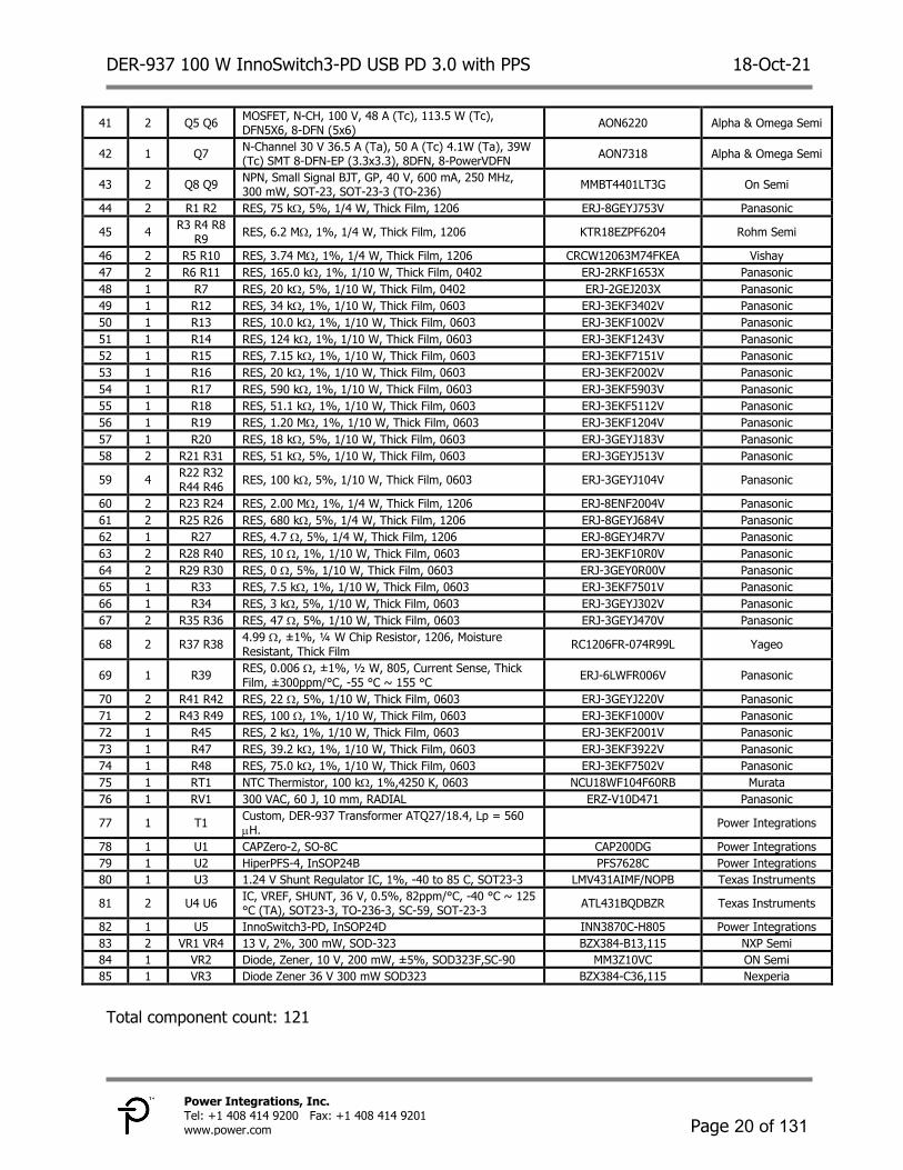
DER-937 100 W InnoSwitch3-PD USB PD 3.0 with PPS 18-Oct-21
Page 20 of 131
Power Integrations, Inc. Tel: +1 408 414 9200 Fax: +1 408 414 9201 www.power.com
41 2 Q5 Q6 MOSFET, N-CH, 100 V, 48 A (Tc), 113.5 W (Tc), DFN5X6, 8-DFN (5x6) AON6220 Alpha & Omega Semi
42 1 Q7 N-Channel 30 V 36.5 A (Ta), 50 A (Tc) 4.1W (Ta), 39W (Tc) SMT 8-DFN-EP (3.3x3.3), 8DFN, 8-PowerVDFN AON7318 Alpha & Omega Semi
43 2 Q8 Q9 NPN, Small Signal BJT, GP, 40 V, 600 mA, 250 MHz, 300 mW, SOT-23, SOT-23-3 (TO-236) MMBT4401LT3G On Semi
44 2 R1 R2 RES, 75 kΩ, 5%, 1/4 W, Thick Film, 1206 ERJ-8GEYJ753V Panasonic
45 4 R3 R4 R8 R9 RES, 6.2 MΩ, 1%, 1/4 W, Thick Film, 1206 KTR18EZPF6204 Rohm Semi
46 2 R5 R10 RES, 3.74 MΩ, 1%, 1/4 W, Thick Film, 1206 CRCW12063M74FKEA Vishay 47 2 R6 R11 RES, 165.0 kΩ, 1%, 1/10 W, Thick Film, 0402 ERJ-2RKF1653X Panasonic 48 1 R7 RES, 20 kΩ, 5%, 1/10 W, Thick Film, 0402 ERJ-2GEJ203X Panasonic 49 1 R12 RES, 34 kΩ, 1%, 1/10 W, Thick Film, 0603 ERJ-3EKF3402V Panasonic 50 1 R13 RES, 10.0 kΩ, 1%, 1/10 W, Thick Film, 0603 ERJ-3EKF1002V Panasonic 51 1 R14 RES, 124 kΩ, 1%, 1/10 W, Thick Film, 0603 ERJ-3EKF1243V Panasonic 52 1 R15 RES, 7.15 kΩ, 1%, 1/10 W, Thick Film, 0603 ERJ-3EKF7151V Panasonic 53 1 R16 RES, 20 kΩ, 1%, 1/10 W, Thick Film, 0603 ERJ-3EKF2002V Panasonic 54 1 R17 RES, 590 kΩ, 1%, 1/10 W, Thick Film, 0603 ERJ-3EKF5903V Panasonic 55 1 R18 RES, 51.1 kΩ, 1%, 1/10 W, Thick Film, 0603 ERJ-3EKF5112V Panasonic 56 1 R19 RES, 1.20 MΩ, 1%, 1/10 W, Thick Film, 0603 ERJ-3EKF1204V Panasonic 57 1 R20 RES, 18 kΩ, 5%, 1/10 W, Thick Film, 0603 ERJ-3GEYJ183V Panasonic 58 2 R21 R31 RES, 51 kΩ, 5%, 1/10 W, Thick Film, 0603 ERJ-3GEYJ513V Panasonic
59 4 R22 R32 R44 R46 RES, 100 kΩ, 5%, 1/10 W, Thick Film, 0603 ERJ-3GEYJ104V Panasonic
60 2 R23 R24 RES, 2.00 MΩ, 1%, 1/4 W, Thick Film, 1206 ERJ-8ENF2004V Panasonic 61 2 R25 R26 RES, 680 kΩ, 5%, 1/4 W, Thick Film, 1206 ERJ-8GEYJ684V Panasonic 62 1 R27 RES, 4.7 Ω, 5%, 1/4 W, Thick Film, 1206 ERJ-8GEYJ4R7V Panasonic 63 2 R28 R40 RES, 10 Ω, 1%, 1/10 W, Thick Film, 0603 ERJ-3EKF10R0V Panasonic 64 2 R29 R30 RES, 0 Ω, 5%, 1/10 W, Thick Film, 0603 ERJ-3GEY0R00V Panasonic 65 1 R33 RES, 7.5 kΩ, 1%, 1/10 W, Thick Film, 0603 ERJ-3EKF7501V Panasonic 66 1 R34 RES, 3 kΩ, 5%, 1/10 W, Thick Film, 0603 ERJ-3GEYJ302V Panasonic 67 2 R35 R36 RES, 47 Ω, 5%, 1/10 W, Thick Film, 0603 ERJ-3GEYJ470V Panasonic
68 2 R37 R38 4.99 Ω, ±1%, ¼ W Chip Resistor, 1206, Moisture Resistant, Thick Film RC1206FR-074R99L Yageo
69 1 R39 RES, 0.006 Ω, ±1%, ½ W, 805, Current Sense, Thick Film, ±300ppm/°C, -55 °C ~ 155 °C ERJ-6LWFR006V Panasonic
70 2 R41 R42 RES, 22 Ω, 5%, 1/10 W, Thick Film, 0603 ERJ-3GEYJ220V Panasonic 71 2 R43 R49 RES, 100 Ω, 1%, 1/10 W, Thick Film, 0603 ERJ-3EKF1000V Panasonic 72 1 R45 RES, 2 kΩ, 1%, 1/10 W, Thick Film, 0603 ERJ-3EKF2001V Panasonic 73 1 R47 RES, 39.2 kΩ, 1%, 1/10 W, Thick Film, 0603 ERJ-3EKF3922V Panasonic 74 1 R48 RES, 75.0 kΩ, 1%, 1/10 W, Thick Film, 0603 ERJ-3EKF7502V Panasonic 75 1 RT1 NTC Thermistor, 100 kΩ, 1%,4250 K, 0603 NCU18WF104F60RB Murata 76 1 RV1 300 VAC, 60 J, 10 mm, RADIAL ERZ-V10D471 Panasonic
77 1 T1 Custom, DER-937 Transformer ATQ27/18.4, Lp = 560 µH. Power Integrations
78 1 U1 CAPZero-2, SO-8C CAP200DG Power Integrations 79 1 U2 HiperPFS-4, InSOP24B PFS7628C Power Integrations 80 1 U3 1.24 V Shunt Regulator IC, 1%, -40 to 85 C, SOT23-3 LMV431AIMF/NOPB Texas Instruments
81 2 U4 U6 IC, VREF, SHUNT, 36 V, 0.5%, 82ppm/°C, -40 °C ~ 125 °C (TA), SOT23-3, TO-236-3, SC-59, SOT-23-3 ATL431BQDBZR Texas Instruments
82 1 U5 InnoSwitch3-PD, InSOP24D INN3870C-H805 Power Integrations 83 2 VR1 VR4 13 V, 2%, 300 mW, SOD-323 BZX384-B13,115 NXP Semi 84 1 VR2 Diode, Zener, 10 V, 200 mW, ±5%, SOD323F,SC-90 MM3Z10VC ON Semi 85 1 VR3 Diode Zener 36 V 300 mW SOD323 BZX384-C36,115 Nexperia
Total component count: 121
DER-937 100 W InnoSwitch3-PD USB PD 3.0 with PPS 18-Oct-21
Page 21 of 131
Power Integrations, Inc. Tel: +1 408 414 9200 Fax: +1 408 414 9201 www.power.com
Common Mode Choke Specifications (L1)
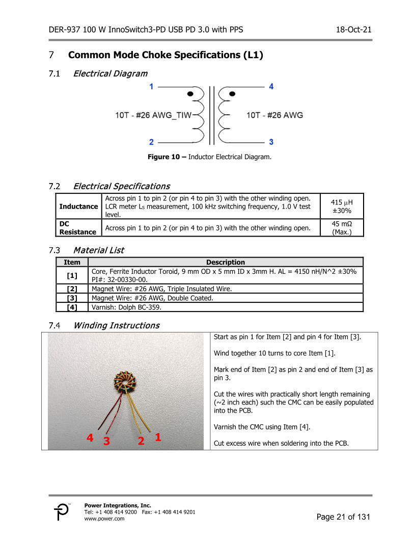
Electrical Diagram
Figure 10 – Inductor Electrical Diagram.
Electrical Specifications
Inductance Across pin 1 to pin 2 (or pin 4 to pin 3) with the other winding open. LCR meter LS measurement, 100 kHz switching frequency, 1.0 V test level.
415 µH ±30%
DC Resistance Across pin 1 to pin 2 (or pin 4 to pin 3) with the other winding open. 45 mΩ
(Max.)
Material List Item Description
[1] Core, Ferrite Inductor Toroid, 9 mm OD x 5 mm ID x 3mm H. AL = 4150 nH/N^2 ±30% PI#: 32-00330-00.
[2] Magnet Wire: #26 AWG, Triple Insulated Wire. [3] Magnet Wire: #26 AWG, Double Coated. [4] Varnish: Dolph BC-359.
Winding Instructions
Start as pin 1 for Item [2] and pin 4 for Item [3]. Wind together 10 turns to core Item [1]. Mark end of Item [2] as pin 2 and end of Item [3] as pin 3. Cut the wires with practically short length remaining (~2 inch each) such the CMC can be easily populated into the PCB. Varnish the CMC using Item [4]. Cut excess wire when soldering into the PCB.
4 1 3 2
DER-937 100 W InnoSwitch3-PD USB PD 3.0 with PPS 18-Oct-21
Page 22 of 131
Power Integrations, Inc. Tel: +1 408 414 9200 Fax: +1 408 414 9201 www.power.com
PFC Inductor Specification (L4)
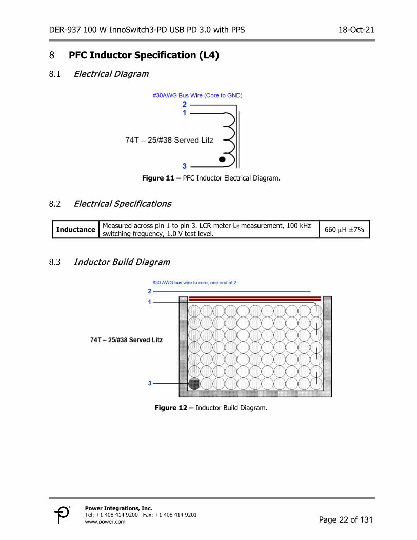
Electrical Diagram
Figure 11 – PFC Inductor Electrical Diagram.
Electrical Specifications
Inductance Measured across pin 1 to pin 3. LCR meter LS measurement, 100 kHz switching frequency, 1.0 V test level. 660 µH ±7%
Inductor Build Diagram
Figure 12 – Inductor Build Diagram.

DER-937 100 W InnoSwitch3-PD USB PD 3.0 with PPS 18-Oct-21
Page 23 of 131
Power Integrations, Inc. Tel: +1 408 414 9200 Fax: +1 408 414 9201 www.power.com
Material List Item Description [1] Core: EQ25, Material 3C95. Ferrox Cube. [2] Bobbin: EQ25, 4 pin (4/0); PI P/N: 25-01141-00. [3] Wire: Served Litz 25/#38. [4] Tape: 3M 1350F-1, Polyester Film, 1 mil Thickness, 8.1 mm Width. [5] Bus Wire: #30 AWG (Solid) Tinned Copper. [6] Tape: 3M 1350F-1, Polyester Film, 1 mil Thickness, 18 mm Width. [7] Varnish: Dolph BC-359, or equivalent.
Winding Instructions
Assign pins 1, 2, and 3. Cut unused pin 4.
Position the bobbin on the mandrel such that the pin side of the bobbin is on the left side. Rotation of the mandrel is clock-wise as seen from the right side of the setup.
Start at pin 3, wind 74 turns of litz wire Item [3]. Wind as illustrated in Figure 3, going from left to right in the first layer, then right to left the next layer, and continue until 74 turns is completed within 7 layers.
x 1 3 2
3
3

DER-937 100 W InnoSwitch3-PD USB PD 3.0 with PPS 18-Oct-21
Page 24 of 131
Power Integrations, Inc. Tel: +1 408 414 9200 Fax: +1 408 414 9201 www.power.com
At the end of last turn, place tape Item [4] to secure the winding, then bring back wire to finish at pin 1. 2 layers of tape Item [4].
Solder the wires to their respective bobbin pins (pin 1 and 3). Add gap to the middle leg of core Item [1] to get 660 µH ±7% inductance. Solder one end of bus wire Item [5] to pin 2 and wrap the bus wire along both core halves.
Secure core halves by wrapping 2 layers of tape Item [6] along the transformer bottom, sides, and top. Ensure inductance is still 660 µH ±7%. Varnish with Item [7] to complete the inductor.
3
1
Bus Wire Item [5]
DER-937 100 W InnoSwitch3-PD USB PD 3.0 with PPS 18-Oct-21
Page 25 of 131
Power Integrations, Inc. Tel: +1 408 414 9200 Fax: +1 408 414 9201 www.power.com
Transformer Specification (T1)
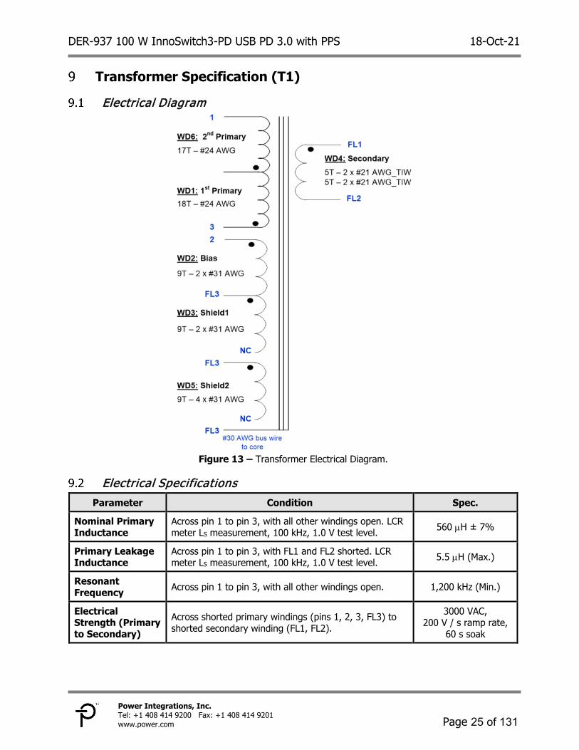
Electrical Diagram
Figure 13 – Transformer Electrical Diagram.
Electrical Specifications Parameter Condition Spec.
Nominal Primary Inductance
Across pin 1 to pin 3, with all other windings open. LCR meter LS measurement, 100 kHz, 1.0 V test level. 560 µH ± 7%
Primary Leakage Inductance
Across pin 1 to pin 3, with FL1 and FL2 shorted. LCR meter LS measurement, 100 kHz, 1.0 V test level. 5.5 µH (Max.)
Resonant Frequency Across pin 1 to pin 3, with all other windings open. 1,200 kHz (Min.)
Electrical Strength (Primary to Secondary)
Across shorted primary windings (pins 1, 2, 3, FL3) to shorted secondary winding (FL1, FL2).
3000 VAC, 200 V / s ramp rate,
60 s soak

DER-937 100 W InnoSwitch3-PD USB PD 3.0 with PPS 18-Oct-21
Page 26 of 131
Power Integrations, Inc. Tel: +1 408 414 9200 Fax: +1 408 414 9201 www.power.com
Transformer Build Diagram
Figure 14 – Transformer Build Diagram.
Material List Item Description [1] Core: ATQ27/18.4, Material KP-95. PI#: 99-00079-00. [2] Bobbin: ATQ27/18.4 horizontal. TBI-238-03381.12XX. PI#: 25-01178-00. [3] Magnet Wire: #24 AWG, Double Coated. [4] Magnet Wire: #31 AWG, Double Coated. [5] Magnet Wire: #21 AWG, Triple Insulated Wire. [6] Bus Wire: #30 AWG (Solid) Tinned Copper. [7] Tape: 3M 1350F-1, Polyester Film, 1 mil Thickness, 10.5 mm Width. [8] Tape: 3M 1350F-1, Polyester Film, 1 mil Thickness, 20.8 mm Width. [9] Varnish: Dolph BC-359.

DER-937 100 W InnoSwitch3-PD USB PD 3.0 with PPS 18-Oct-21
Page 27 of 131
Power Integrations, Inc. Tel: +1 408 414 9200 Fax: +1 408 414 9201 www.power.com
Winding Instructions
Bobbin and Winding
Preparation
Position the bobbin on the mandrel such that the pin side of the bobbin is on the left side. Rotation of the mandrel is clock-wise as seen from the right side of the set-up.
WD1 1st Primary
Start at pin 3, enter wire to bobbin slot 4, and wind 18 turns of wire Item [3] in 1 layer, from left to right.
Insulation
At the end of last turn, place tape Item [7] to secure the winding, then bring back wire to the left side bobbin Slot 3. Leave enough wire for the 2nd half Primary (17 turns) to be wound later.
1 layer of tape Item [7].
1 2 3
Pin 3
Slot 4
Slot 1
Slot 3
DER-937 100 W InnoSwitch3-PD USB PD 3.0 with PPS 18-Oct-21
Page 28 of 131
Power Integrations, Inc. Tel: +1 408 414 9200 Fax: +1 408 414 9201 www.power.com
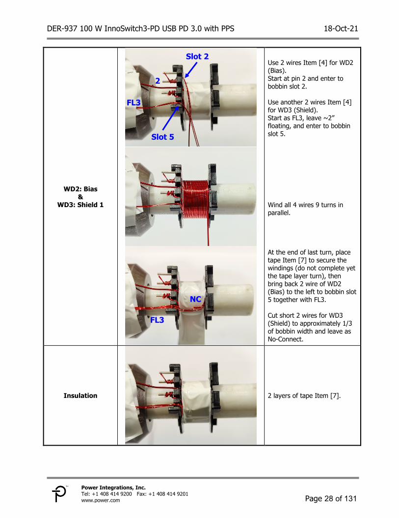
WD2: Bias &
WD3: Shield 1
Use 2 wires Item [4] for WD2 (Bias). Start at pin 2 and enter to bobbin slot 2. Use another 2 wires Item [4] for WD3 (Shield). Start as FL3, leave ~2” floating, and enter to bobbin slot 5. Wind all 4 wires 9 turns in parallel. At the end of last turn, place tape Item [7] to secure the windings (do not complete yet the tape layer turn), then bring back 2 wire of WD2 (Bias) to the left to bobbin slot 5 together with FL3. Cut short 2 wires for WD3 (Shield) to approximately 1/3 of bobbin width and leave as No-Connect.
Insulation
2 layers of tape Item [7].
NC
FL3
2
FL3
Slot 2
Slot 5

DER-937 100 W InnoSwitch3-PD USB PD 3.0 with PPS 18-Oct-21
Page 29 of 131
Power Integrations, Inc. Tel: +1 408 414 9200 Fax: +1 408 414 9201 www.power.com
WD4 Secondary
Start at the secondary left slot of the bobbin. Use 2 wires Item [5], leave ~2” floating, and mark as FL1. Wind 5 turns in 1 layer. At the end of last turn, exit the wires at the right slot, leave ~2” floating and mark as FL2 for 1st half of Secondary. Repeat another winding same as above for 2nd half of Secondary, which is parallel with 1st half Secondary.
FL1
FL1
FL2 FL1
FL1 FL2

DER-937 100 W InnoSwitch3-PD USB PD 3.0 with PPS 18-Oct-21
Page 30 of 131
Power Integrations, Inc. Tel: +1 408 414 9200 Fax: +1 408 414 9201 www.power.com
Insulation
2 layers of tape Item [7].
WD5 Shield2
Use 4 wires Item [4] for WD5 (Shield 2). Start with FL3, enter to bobbin slot 5, and wind 9 turns in parallel.
At the end of last turn, place tape Item [7] to secure the winding (do not complete yet the tape layer turn). Then cut short the 4 wires to approximately 1/3 of bobbin width and leave as No-Connect.
FL3
FL3
NC
Slot 5

DER-937 100 W InnoSwitch3-PD USB PD 3.0 with PPS 18-Oct-21
Page 31 of 131
Power Integrations, Inc. Tel: +1 408 414 9200 Fax: +1 408 414 9201 www.power.com
Insulation
1 layer of tape Item [7].
WD6 2nd Primary
Use wire hanging from WD1 (Primary) and continue winding 17 turns from left to right.
At the end of last turn, place tape Item [7] to secure the winding (do not complete yet the tape layer turn), then finish winding at pin 1 through slot 1.
Slot 1
Pin 1

DER-937 100 W InnoSwitch3-PD USB PD 3.0 with PPS 18-Oct-21
Page 32 of 131
Power Integrations, Inc. Tel: +1 408 414 9200 Fax: +1 408 414 9201 www.power.com
Insulation
2 layers of tape Item [7].
WD4 Secondary
Bring all 4 wires of Secondary Winding FL1 from left slot to exit to the right slot.
Insulation
2 layers of tape Item [7].
FL1

DER-937 100 W InnoSwitch3-PD USB PD 3.0 with PPS 18-Oct-21
Page 33 of 131
Power Integrations, Inc. Tel: +1 408 414 9200 Fax: +1 408 414 9201 www.power.com
Gap and Ground Core
Solder the wires to their respective bobbin pins (pin 1, 2, 3). Add gap to the middle leg of core Item [1] to get 560 µH ±7% primary inductance. Twist one end of bus wire Item [6] together with FL3 and wrap the bus wire along both core halves. Secure core halves by wrapping 2 layers of tape Item [8] along the transformer bottom, sides, and top. Ensure primary inductance is still 560 µH ±7%.
Tape for Core Insulation
Cover the transformer core bottom and secondary side with 2 layers of tape Item [8] for improved ESD performance. Align the tape such it covers about 1/3 of the core bottom surface.
Fold the excess tape to cover secondary side.
2-layer Item [8]
Bus Wire Item [6]

DER-937 100 W InnoSwitch3-PD USB PD 3.0 with PPS 18-Oct-21
Page 34 of 131
Power Integrations, Inc. Tel: +1 408 414 9200 Fax: +1 408 414 9201 www.power.com
Secure the assembly with 1 layer of tape Item [8] along the transformer sides.
Finish Assembly
Twist together the 4 wires of FL1. Also twist together the 4 wires of FL2. Varnish with Item [9] to complete the transformer. Cut excess fly lead wire after soldering the transformer into the PCB.
Item [8]
DER-937 100 W InnoSwitch3-PD USB PD 3.0 with PPS 18-Oct-21
Page 35 of 131
Power Integrations, Inc. Tel: +1 408 414 9200 Fax: +1 408 414 9201 www.power.com
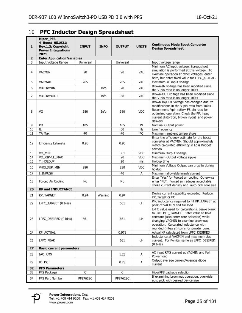
PFC Inductor Design Spreadsheet
1
Hiper_PFS-4_Boost_051921; Rev.1.3; Copyright Power Integrations 2021
INPUT INFO OUTPUT UNITS Continuous Mode Boost Converter Design Spreadsheet
2 Enter Application Variables 3 Input Voltage Range Universal Universal Input voltage range
4 VACMIN 90 90 VAC Minimum AC input voltage. Spreadsheet simulation is performed at this voltage. To examine operation at other votlages, enter here, but enter fixed value for LPFC_ACTUAL.
5 VACMAX 265 265 VAC Maximum AC input voltage
6 VBROWNIN Info 78 VAC Brown-IN voltage has been modified since the V-pin ratio is no longer 100:1
7 VBROWNOUT Info 68 VAC Brown-OUT voltage has been modified since the V-pin ratio is no longer 100:1
8 VO 380 Info 380 VDC
Brown IN/OUT voltage has changed due to modifications in the V-pin ratio from 100:1. Recommend Vpin ratio= FB pin ratio for optimized operation. Check the PF, input current distortion, brown in/out and power delivery
9 PO 105 105 W Nominal Output power 10 fL 50 Hz Line frequency 11 TA Max 40 40 °C Maximum ambient temperature
12 Efficiency Estimate 0.95 0.95 Enter the efficiency estimate for the boost converter at VACMIN. Should approximately match calculated efficiency in Loss Budget section
13 VO_MIN 361 VDC Minimum Output voltage 14 VO_RIPPLE_MAX 20 VDC Maximum Output voltage ripple 15 T_HOLDUP 20 ms Holdup time
16 VHOLDUP_MIN 280 280 VDC Minimum Voltage Output can drop to during holdup
17 I_INRUSH 40 A Maximum allowable inrush current
18 Forced Air Cooling No No Enter "Yes" for Forced air cooling. Otherwise enter "No". Forced air reduces acceptable choke current density and auto pick core size
20 KP and INDUCTANCE
21 KP_TARGET 0.94 Warning 0.94 Device current capability exceeded. Reduce KP_Target or PO
22 LPFC_TARGET (0 bias) 661 uH PFC inductance required to hit KP_TARGET at peak of VACMIN and full load
23 LPFC_DESIRED (0 bias) 661 661 uH
LPFC value used for calculations. Leave blank to use LPFC_TARGET. Enter value to hold constant (also enter core selection) while changing VACMIN to examine brownout operation. Calculated inductance with rounded (integral) turns for powder core.
24 KP_ACTUAL 0.978 Actual KP calculated from LPFC_DESIRED
25 LPFC_PEAK 661 uH Inductance at VACMIN and maximum bias current. For Ferrite, same as LPFC_DESIRED (0 bias)
27 Basic current parameters
28 IAC_RMS 1.23 A AC input RMS current at VACMIN and Full Power load
29 IO_DC 0.28 A Output average current/Average diode current
32 PFS Parameters 33 PFS Package C C HiperPFS package selection
34 PFS Part Number PFS7628C PFS7628C If examining brownout operation, over-ride auto pick with desired device size
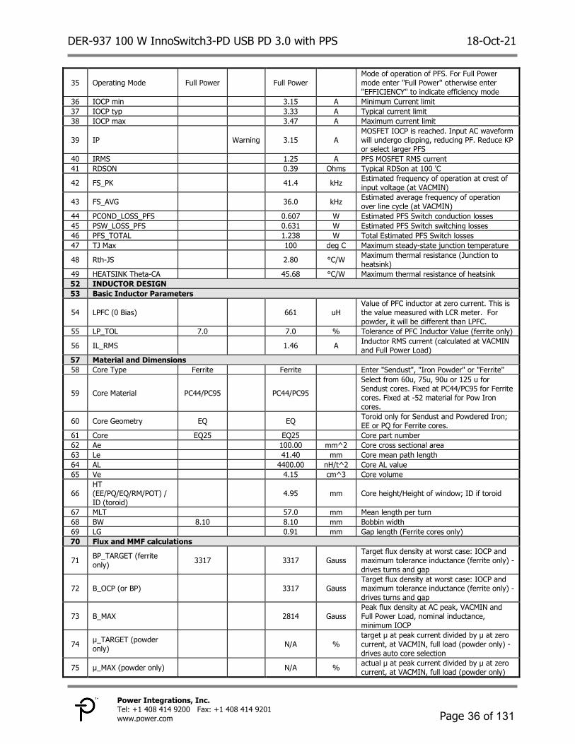
DER-937 100 W InnoSwitch3-PD USB PD 3.0 with PPS 18-Oct-21
Page 36 of 131
Power Integrations, Inc. Tel: +1 408 414 9200 Fax: +1 408 414 9201 www.power.com
35 Operating Mode Full Power Full Power Mode of operation of PFS. For Full Power mode enter ''Full Power'' otherwise enter ''EFFICIENCY'' to indicate efficiency mode
36 IOCP min 3.15 A Minimum Current limit 37 IOCP typ 3.33 A Typical current limit 38 IOCP max 3.47 A Maximum current limit
39 IP Warning 3.15 A MOSFET IOCP is reached. Input AC waveform will undergo clipping, reducing PF. Reduce KP or select larger PFS
40 IRMS 1.25 A PFS MOSFET RMS current 41 RDSON 0.39 Ohms Typical RDSon at 100 'C
42 FS_PK 41.4 kHz Estimated frequency of operation at crest of input voltage (at VACMIN)
43 FS_AVG 36.0 kHz Estimated average frequency of operation over line cycle (at VACMIN)
44 PCOND_LOSS_PFS 0.607 W Estimated PFS Switch conduction losses 45 PSW_LOSS_PFS 0.631 W Estimated PFS Switch switching losses 46 PFS_TOTAL 1.238 W Total Estimated PFS Switch losses 47 TJ Max 100 deg C Maximum steady-state junction temperature
48 Rth-JS 2.80 °C/W Maximum thermal resistance (Junction to heatsink)
49 HEATSINK Theta-CA 45.68 °C/W Maximum thermal resistance of heatsink 52 INDUCTOR DESIGN 53 Basic Inductor Parameters
54 LPFC (0 Bias) 661 uH Value of PFC inductor at zero current. This is the value measured with LCR meter. For powder, it will be different than LPFC.
55 LP_TOL 7.0 7.0 % Tolerance of PFC Inductor Value (ferrite only)
56 IL_RMS 1.46 A Inductor RMS current (calculated at VACMIN and Full Power Load)
57 Material and Dimensions 58 Core Type Ferrite Ferrite Enter "Sendust", "Iron Powder" or "Ferrite"
59 Core Material PC44/PC95 PC44/PC95 Select from 60u, 75u, 90u or 125 u for Sendust cores. Fixed at PC44/PC95 for Ferrite cores. Fixed at -52 material for Pow Iron cores.
60 Core Geometry EQ EQ Toroid only for Sendust and Powdered Iron; EE or PQ for Ferrite cores.
61 Core EQ25 EQ25 Core part number 62 Ae 100.00 mm^2 Core cross sectional area 63 Le 41.40 mm Core mean path length 64 AL 4400.00 nH/t^2 Core AL value 65 Ve 4.15 cm^3 Core volume
66 HT (EE/PQ/EQ/RM/POT) / ID (toroid)
4.95 mm Core height/Height of window; ID if toroid
67 MLT 57.0 mm Mean length per turn 68 BW 8.10 8.10 mm Bobbin width 69 LG 0.91 mm Gap length (Ferrite cores only) 70 Flux and MMF calculations
71 BP_TARGET (ferrite only) 3317 3317 Gauss
Target flux density at worst case: IOCP and maximum tolerance inductance (ferrite only) - drives turns and gap
72 B_OCP (or BP) 3317 Gauss Target flux density at worst case: IOCP and maximum tolerance inductance (ferrite only) - drives turns and gap
73 B_MAX 2814 Gauss Peak flux density at AC peak, VACMIN and Full Power Load, nominal inductance, minimum IOCP
74 µ_TARGET (powder only)
N/A % target µ at peak current divided by µ at zero current, at VACMIN, full load (powder only) - drives auto core selection
75 µ_MAX (powder only) N/A % actual µ at peak current divided by µ at zero current, at VACMIN, full load (powder only)

DER-937 100 W InnoSwitch3-PD USB PD 3.0 with PPS 18-Oct-21
Page 37 of 131
Power Integrations, Inc. Tel: +1 408 414 9200 Fax: +1 408 414 9201 www.power.com
76 µ_OCP (powder only) N/A % µ at IOC Ptyp divided by µ at zero current
77 I_TEST 3.3 A
Current at which B_TEST and H_TEST are calculated, for checking flux at a current other than IOCP or IP; if blank IOCP_typ is used.
78 B_TEST 3183 Gauss Flux density at I_TEST and maximum tolerance inductance
79 µ_TEST (powder only) N/A % µ at IOCP divided by µ at zero current, at IOCPtyp
80 Wire
81 TURNS 74 Inductor turns. To adjust turns, change BP_TARGET (ferrite) or µ_TARGET (powder)
82 ILRMS 1.46 A Inductor RMS current
83 Wire type Litz Litz Select between "Litz" or "Magnet" for double coated magnet wire
84 AWG 38 38 AWG Inductor wire gauge
85 Filar 25 25 Inductor wire number of parallel strands. Leave blank to auto-calc for Litz
86 OD (per strand) 0.102 mm Outer diameter of single strand of wire 87 OD bundle (Litz only) 0.71 mm Will be different than OD if Litz 88 DCR 0.464 ohm Choke DC Resistance
89 P AC Resistance Ratio 1.13 Ratio of total copper loss, including HF AC, to the DC component of the loss
90 J Warning 7.22 A/mm^2 Current density is high, if copper loss is high use thicker wire, more strands, or larger core
91 FIT 93 % Percentage fill of winding window for EE/PQ core. Full window approx. 90%
92 Layers 6.85 Estimated layers in winding 93 Loss calculations
94 BAC-p-p 2752 Gauss Core AC peak-peak flux excursion at VACMIN, peak of sine wave
95 LPFC_CORE_LOSS 0.075 W Estimated Inductor core Loss 96 LPFC_COPPER_LOSS 1.128 W Estimated Inductor copper losses 97 LPFC_TOTAL_LOSS 1.203 W Total estimated Inductor Losses
100 PFC Diode 101 PFC Diode Part Number STTH3R06 STTH3R06 PFS Diode Part Number 102 Type / Part Number ULTRAFAST PFC Diode Type / Part Number 103 Manufacturer ST Diode Manufacturer 104 VRRM 600.0 V Diode rated reverse voltage 105 IF 3.00 A Diode rated forward current 106 Qrr Info 190.0 nC Qrr too high: Will result in high diode loss 107 VF 1.25 V Diode rated forward voltage drop 108 PCOND_DIODE 0.368 W Estimated Diode conduction losses 109 PSW_DIODE 0.111 W Estimated Diode switching losses 110 P_DIODE 0.479 W Total estimated Diode losses 111 TJ Max 100.0 deg C Maximum steady-state operating temperature 112 Rth-JS Info 20.00 degC/W Rth too high. Will result in high diode loss 113 HEATSINK Theta-CA 104.89 degC/W Maximum thermal resistance of heatsink
114 IFSM 55.0 A Non-repetitive peak surge current rating. Consider larger size diode if inrush or thermal limited.
117 Output Capacitor 118 COUT 100 100 uF Minimum value of Output capacitance
119 VO_RIPPLE_EXPECTED 9.3 V Expected ripple voltage on Output with selected Output capacitor
120 T_HOLDUP_EXPECTED 31.4 ms Expected holdup time with selected Output capacitor
121 ESR_LF 2.93 ohms Low Frequency Capacitor ESR
122 ESR_HF Warning 1.17 ohms High frequency ESR must be between 0.01 and 1 ohms
123 IC_RMS_LF 0.19 A Low Frequency Capacitor RMS current 124 IC_RMS_HF 0.67 A High Frequency Capacitor RMS current

DER-937 100 W InnoSwitch3-PD USB PD 3.0 with PPS 18-Oct-21
Page 38 of 131
Power Integrations, Inc. Tel: +1 408 414 9200 Fax: +1 408 414 9201 www.power.com
125 CO_LF_LOSS 0.106 W Estimated Low Frequency ESR loss in Output capacitor
126 CO_HF_LOSS 0.525 W Estimated High frequency ESR loss in Output capacitor
127 Total CO LOSS 0.632 W Total estimated losses in Output Capacitor 130 Input Bridge (BR1) and Fuse (F1) 131 I^2t Rating 7.02 A^2*s Minimum I^2t rating for fuse 132 Fuse Current rating 1.98 A Minimum Current rating of fuse 133 VF 0.90 V Input bridge Diode forward Diode drop 134 IAVG 1.23 A Input average current at VBROWNOUT. 135 PIV_INPUT BRIDGE 375 V Peak inverse voltage of input bridge 136 PCOND_LOSS_BRIDGE 1.990 W Estimated Bridge Diode conduction loss
137 CIN 0.33 uF Input capacitor. Use metallized polypropylene or film foil type with high ripple current rating
138 CIN_DF 0.001 Input Capacitor Dissipation Factor (tan Delta) 139 CIN_PLOSS 0.009 W Input Capacitor Loss 140 RT1 9.37 ohms Input Thermistor value 141 D_Precharge 1N5407 Recommended precharge Diode 144 PFS4 small signal components 145 C_REF 1.0 uF REF pin capacitor value 146 RV1 4.0 MOhms Line sense resistor 1 147 RV2 6.0 MOhms Line sense resistor 2
148 RV3 6.0 MOhms Typical value of the lower resistor connected to the V-PIN. Use 1% resistor only!
149 RV4 163.8 kOhms Description pending, could be modified based on feedback chain R1-R4
150 C_V 0.489 nF V pin decoupling capacitor (RV4 and C_V should have a time constant of 80us) Pick the closest available capacitance.
151 C_VCC 1.0 uF Supply decoupling capacitor 152 C_C 100 nF Feedback C pin decoupling capacitor
153 Power good Vo lower threshold VPG(L)
333 V Vo lower threshold voltage at which power good signal will trigger
154 PGT set resistor 337.4 kohm Power good threshold setting resistor 157 Feedback Components
158 RFB_1 4.00 Mohms Feedback network, first high voltage divider resistor
159 RFB_2 6.00 Mohms Feedback network, second high voltage divider resistor
160 RFB_3 6.00 Mohms Feedback network, third high voltage divider resistor
161 RFB_4 163.8 kohms Feedback network, lower divider resistor
162 CFB_1 0.489 nF Feedback network, loop speedup capacitor. (R4 and C1 should have a time constant of 80us) Pick the closest available capacitance.
163 RFB_5 35.7 kohms Feedback network: zero setting resistor
164 CFB_2 1000 nF Feedback component- noise suppression capacitor
167 Loss Budget (Estimated at VACMIN) 168 PFS Losses 1.238 W Total estimated losses in PFS 169 Boost diode Losses 0.479 W Total estimated losses in Output Diode 170 Input Bridge losses 1.990 W Total estimated losses in input bridge module 171 Input Capacitor Losses 0.009 W Total estimated losses in input capacitor 172 Inductor losses 1.203 W Total estimated losses in PFC choke 173 Output Capacitor Loss 0.632 W Total estimated losses in Output capacitor 174 EMI choke copper loss 0.151 W Total estimated losses in EMI choke copper 175 Total losses 5.701 W Overall loss estimate 176 Efficiency 0.95 Estimated efficiency at VACMIN, full load. 179 CAPZero component selection recommendation
180 CAPZero Device CAP200DG (Optional) Recommended CAPZero device to discharge X-Capacitor with time constant of 1 second
DER-937 100 W InnoSwitch3-PD USB PD 3.0 with PPS 18-Oct-21
Page 39 of 131
Power Integrations, Inc. Tel: +1 408 414 9200 Fax: +1 408 414 9201 www.power.com
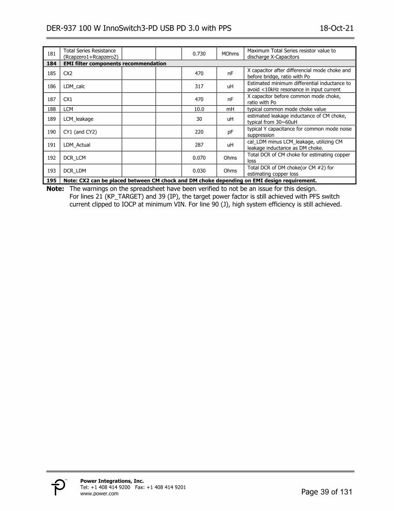
181 Total Series Resistance (Rcapzero1+Rcapzero2)
0.730 MOhms Maximum Total Series resistor value to discharge X-Capacitors
184 EMI filter components recommendation
185 CX2 470 nF X capacitor after differencial mode choke and before bridge, ratio with Po
186 LDM_calc 317 uH Estimated minimum differential inductance to avoid <10kHz resonance in input current
187 CX1 470 nF X capacitor before common mode choke, ratio with Po
188 LCM 10.0 mH typical common mode choke value
189 LCM_leakage 30 uH estimated leakage inductance of CM choke, typical from 30~60uH
190 CY1 (and CY2) 220 pF typical Y capacitance for common mode noise suppression
191 LDM_Actual 287 uH cal_LDM minus LCM_leakage, utilizing CM leakage inductance as DM choke.
192 DCR_LCM 0.070 Ohms Total DCR of CM choke for estimating copper loss
193 DCR_LDM 0.030 Ohms Total DCR of DM choke(or CM #2) for estimating copper loss
195 Note: CX2 can be placed between CM chock and DM choke depending on EMI design requirement. Note: The warnings on the spreadsheet have been verified to not be an issue for this design.
For lines 21 (KP_TARGET) and 39 (IP), the target power factor is still achieved with PFS switch current clipped to IOCP at minimum VIN. For line 90 (J), high system efficiency is still achieved.
DER-937 100 W InnoSwitch3-PD USB PD 3.0 with PPS 18-Oct-21
Page 40 of 131
Power Integrations, Inc. Tel: +1 408 414 9200 Fax: +1 408 414 9201 www.power.com
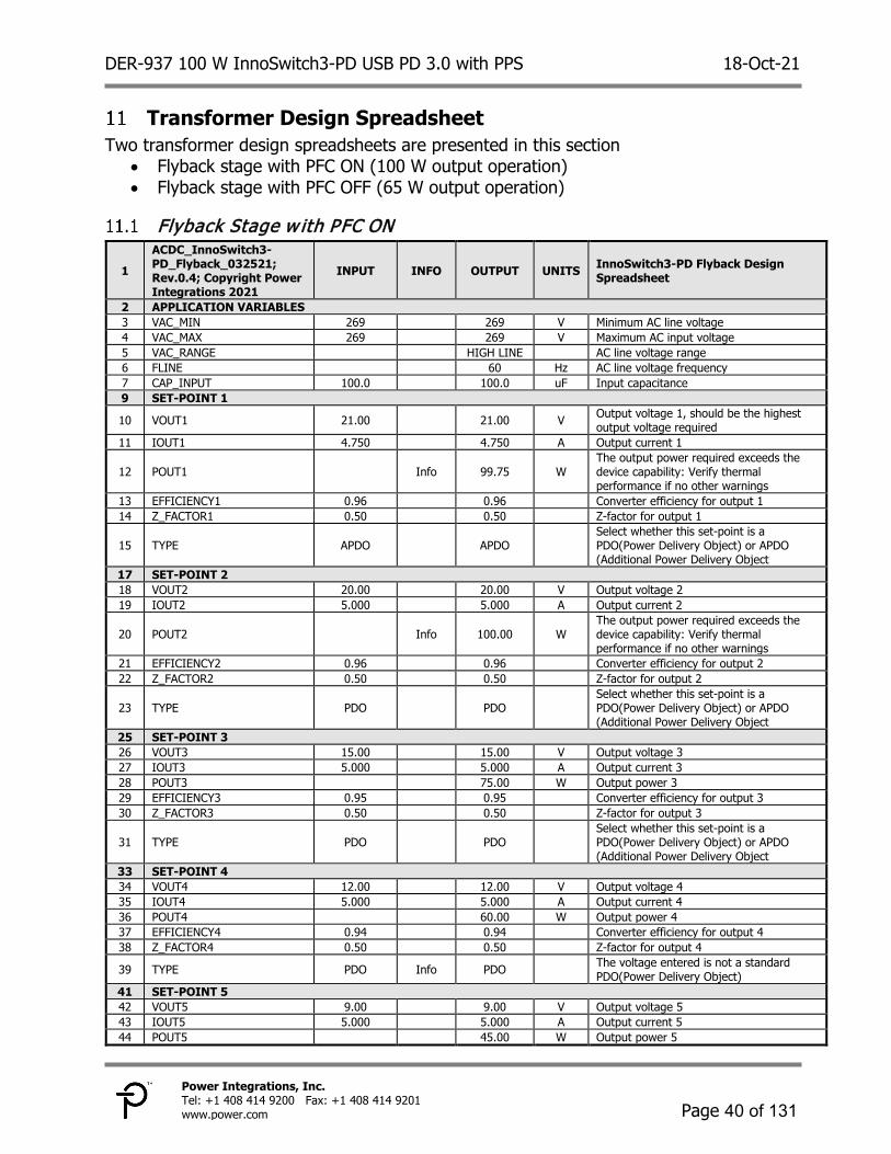
Transformer Design Spreadsheet Two transformer design spreadsheets are presented in this section
• Flyback stage with PFC ON (100 W output operation) • Flyback stage with PFC OFF (65 W output operation)
Flyback Stage w ith PFC ON
1
ACDC_InnoSwitch3-PD_Flyback_032521; Rev.0.4; Copyright Power Integrations 2021
INPUT INFO OUTPUT UNITS InnoSwitch3-PD Flyback Design Spreadsheet
2 APPLICATION VARIABLES 3 VAC_MIN 269 269 V Minimum AC line voltage 4 VAC_MAX 269 269 V Maximum AC input voltage 5 VAC_RANGE HIGH LINE AC line voltage range 6 FLINE 60 Hz AC line voltage frequency 7 CAP_INPUT 100.0 100.0 uF Input capacitance 9 SET-POINT 1
10 VOUT1 21.00 21.00 V Output voltage 1, should be the highest output voltage required
11 IOUT1 4.750 4.750 A Output current 1
12 POUT1 Info 99.75 W The output power required exceeds the device capability: Verify thermal performance if no other warnings
13 EFFICIENCY1 0.96 0.96 Converter efficiency for output 1 14 Z_FACTOR1 0.50 0.50 Z-factor for output 1
15 TYPE APDO APDO Select whether this set-point is a PDO(Power Delivery Object) or APDO (Additional Power Delivery Object
17 SET-POINT 2 18 VOUT2 20.00 20.00 V Output voltage 2 19 IOUT2 5.000 5.000 A Output current 2
20 POUT2 Info 100.00 W The output power required exceeds the device capability: Verify thermal performance if no other warnings
21 EFFICIENCY2 0.96 0.96 Converter efficiency for output 2 22 Z_FACTOR2 0.50 0.50 Z-factor for output 2
23 TYPE PDO PDO Select whether this set-point is a PDO(Power Delivery Object) or APDO (Additional Power Delivery Object
25 SET-POINT 3 26 VOUT3 15.00 15.00 V Output voltage 3 27 IOUT3 5.000 5.000 A Output current 3 28 POUT3 75.00 W Output power 3 29 EFFICIENCY3 0.95 0.95 Converter efficiency for output 3 30 Z_FACTOR3 0.50 0.50 Z-factor for output 3
31 TYPE PDO PDO Select whether this set-point is a PDO(Power Delivery Object) or APDO (Additional Power Delivery Object
33 SET-POINT 4 34 VOUT4 12.00 12.00 V Output voltage 4 35 IOUT4 5.000 5.000 A Output current 4 36 POUT4 60.00 W Output power 4 37 EFFICIENCY4 0.94 0.94 Converter efficiency for output 4 38 Z_FACTOR4 0.50 0.50 Z-factor for output 4
39 TYPE PDO Info PDO The voltage entered is not a standard PDO(Power Delivery Object)
41 SET-POINT 5 42 VOUT5 9.00 9.00 V Output voltage 5 43 IOUT5 5.000 5.000 A Output current 5 44 POUT5 45.00 W Output power 5

DER-937 100 W InnoSwitch3-PD USB PD 3.0 with PPS 18-Oct-21
Page 41 of 131
Power Integrations, Inc. Tel: +1 408 414 9200 Fax: +1 408 414 9201 www.power.com
45 EFFICIENCY5 0.93 0.93 Converter efficiency for output 5 46 Z_FACTOR5 0.50 0.50 Z-factor for output 5
47 TYPE PDO PDO Select whether this set-point is a PDO(Power Delivery Object) or APDO (Additional Power Delivery Object
49 SET-POINT 6 50 VOUT6 5.00 5.00 V Output voltage 6 51 IOUT6 5.000 5.000 A Output current 6 52 POUT6 25.00 W Output power 6 53 EFFICIENCY6 0.92 0.92 Converter efficiency for output 6 54 Z_FACTOR6 0.50 0.50 Z-factor for output 6
55 TYPE PDO PDO Select whether this set-point is a PDO(Power Delivery Object) or APDO (Additional Power Delivery Object
57 SET-POINT 7 58 VOUT7 3.30 3.30 V Output voltage 7 59 IOUT7 5.000 5.000 A Output current 7 60 POUT7 16.50 W Output power 7 61 EFFICIENCY7 0.89 0.89 Converter efficiency for output 7 62 Z_FACTOR7 0.50 0.50 Z-factor for output 7
63 TYPE APDO APDO Select whether this set-point is a PDO(Power Delivery Object) or APDO (Additional Power Delivery Object
81 VOLTAGE_CDC 0.000 0.000 V Cable drop compensation desired at maximum output current
85 PRIMARY CONTROLLER SELECTION 86 ENCLOSURE ADAPTER ADAPTER Power supply enclosure 87 ILIMIT_MODE INCREASED INCREASED Device current limit mode 88 VDRAIN_BREAKDOWN 750 750 V Device breakdown voltage 89 DEVICE_GENERIC INN38X0 INN38X0 Device selection 90 DEVICE_CODE INN3870C Device code 91 PDEVICE_MAX 90 W Device maximum power capability 92 RDSON_25DEG 0.39 Ω Primary switch on-time resistance at 25°C 93 RDSON_100DEG 0.54 Ω Primary switch on-time resistance at 100°C 94 ILIMIT_MIN 2.395 A Primary switch minimum current limit 95 ILIMIT_TYP 2.576 A Primary switch typical current limit 96 ILIMIT_MAX 2.756 A Primary switch maximum current limit 97 VDRAIN_ON_PRSW 0.15 V Primary switch on-time voltage drop
98 VDRAIN_OFF_PRSW 595.966 V Peak drain voltage on the primary switch during turn-off
102 WORST CASE ELECTRICAL PARAMETERS
103 FSWITCHING_MAX 73289 Info 73289 Hz The worst case minimum operating frequency is less than 25kHz: may result in audible noise
104 VOR 147.0 147.0 V Voltage reflected to the primary winding (corresponding to set-point 1) when the primary switch turns off
105 VMIN 380.00 Info 380.00 V A manual overwrite of VMIN voids the value of input capacitor calculated by the tool or manually entered by the user and will be used for all calculations
106 KP 1.026 Measure of continuous/discontinuous mode of operation
107 MODE_OPERATION DCM Mode of operation 108 DUTYCYCLE 0.236 Primary switch duty cycle 109 TIME_ON 3.99 us Primary switch on-time 110 TIME_OFF 10.47 us Primary switch off-time 111 LPRIMARY_MIN 521.0 uH Minimum primary magnetizing inductance 112 LPRIMARY_TYP 560.2 uH Typical primary magnetizing inductance 113 LPRIMARY_TOL 7.0 7.0 % Primary magnetizing inductance tolerance 114 LPRIMARY_MAX 599.5 uH Maximum primary magnetizing inductance 116 PRIMARY CURRENT 117 IAVG_PRIMARY 0.269 A Primary switch average current
DER-937 100 W InnoSwitch3-PD USB PD 3.0 with PPS 18-Oct-21
Page 42 of 131
Power Integrations, Inc. Tel: +1 408 414 9200 Fax: +1 408 414 9201 www.power.com
118 IPEAK_PRIMARY 2.575 A Primary switch peak current 119 IPEDESTAL_PRIMARY 0.000 A Primary switch current pedestal 120 IRIPPLE_PRIMARY 2.575 A Primary switch ripple current 121 IRMS_PRIMARY 0.679 A Primary switch RMS current 123 SECONDARY CURRENT 124 IPEAK_SECONDARY 18.022 A Secondary winding peak current 125 IPEDESTAL_SECONDARY 0.000 A Secondary winding pedestal current 126 IRMS_SECONDARY 7.830 A Secondary winding RMS current 127 IRIPPLE_CAP_OUT 6.026 A Output capacitor ripple current 131 TRANSFORMER CONSTRUCTION PARAMETERS 132 CORE SELECTION
133 CORE ATQ27/18 Info ATQ27/18 Refer to the Transformer Parameters tab to verify fit factor
134 CORE NAME ATQ27/18 Core code 135 AE 131.0 mm^2 Core cross sectional area 136 LE 50.8 mm Core magnetic path length
137 AL 7350 nH/t^2 Ungapped core effective inductance per turns squared
138 VE 6655 mm^3 Core volume
139 BOBBIN NAME TBI-238-03381.12XX
Bobbin name
140 AW 51.0 mm^2 Bobbin window area 141 BW 10.40 mm Bobbin width 142 MARGIN 0.0 mm Bobbin safety margin 144 PRIMARY WINDING 145 NPRIMARY 35 Primary winding number of turns 146 BPEAK 3688 Gauss Peak flux density 147 BMAX 3303 Gauss Maximum flux density 148 BAC 1652 Gauss AC flux density (0.5 x Peak to Peak)
149 ALG 457 nH/t^2 Typical gapped core effective inductance per turns squared
150 LG 0.338 mm Core gap length 151 LAYERS_PRIMARY 2 2 Primary winding number of layers 152 AWG_PRIMARY 24 Primary wire gauge 153 OD_PRIMARY_INSULATED 0.577 mm Primary wire insulated outer diameter 154 OD_PRIMARY_BARE 0.511 mm Primary wire bare outer diameter
155 CMA_PRIMARY Info 594.9 Cmils/A The primary winding wire CMA is higher than 500 mil^2/Amperes: Decrease the primary layers or wire thickness
157 SECONDARY WINDING 158 NSECONDARY 5 5 Secondary winding number of turns 159 AWG_SECONDARY 18 Secondary wire gauge 160 OD_SECONDARY_INSULATED 1.328 mm Secondary wire insulated outer diameter 161 OD_SECONDARY_BARE 1.024 mm Secondary wire bare outer diameter 162 CMA_SECONDARY 207.4 Cmils/A Secondary winding wire CMA 164 BIAS WINDING 165 NBIAS 10 Bias winding number of turns 169 PRIMARY COMPONENTS SELECTION 170 LINE UNDERVOLTAGE 171 BROWN-IN REQURED 76.00 76.00 V Required line brown-in threshold
172 RLS 4.00 MΩ Connect two 2 MOhm resistors to the V-pin for the required UV/OV threshold
173 BROWN-IN ACTUAL 75.98 V Actual brown-in threshold using standard resistors
174 BROWN-OUT ACTUAL 66.93 V Actual brown-out threshold using standard resistors
176 LINE OVERVOLTAGE
177 OVERVOLTAGE_LINE Warning 334.21 V The device voltage stress will be higher than 650V when overvoltage is triggered
179 BIAS WINDING
180 VBIAS 9.00 V Rectified bias voltage at the cable disconnect (5V) set-point
181 VF_BIAS 0.70 V Bias winding diode forward drop

DER-937 100 W InnoSwitch3-PD USB PD 3.0 with PPS 18-Oct-21
Page 43 of 131
Power Integrations, Inc. Tel: +1 408 414 9200 Fax: +1 408 414 9201 www.power.com
182 VREVERSE_BIASDIODE 117.28 V Bias diode reverse voltage (not accounting parasitic voltage ring)
183 CBIAS 22 uF Bias winding rectification capacitor 184 CBPP 4.70 uF BPP pin capacitor 188 SECONDARY COMPONENTS SELECTION 189 RECTIFIER
190 VDRAIN_OFF_SRFET 75.14 V Secondary rectifier reverse voltage (not accounting parasitic voltage ring)
191 SRFET AON6220 AON6220 Secondary rectifier (Logic MOSFET) 192 VBREAKDOWN_SRFET 100 V Secondary rectifier breakdown voltage
193 RDSON_SRFET 7.4 mΩ SRFET on time drain resistance at 25degC for VGS=4.4V
Note: The warnings on the spreadsheet have been verified to not be an issue for this design. For line 177 (OVERVOLTAGE_LINE), the InnoSwitch3-PD INN3870C-H805 is a 750 V device.

DER-937 100 W InnoSwitch3-PD USB PD 3.0 with PPS 18-Oct-21
Page 44 of 131
Power Integrations, Inc. Tel: +1 408 414 9200 Fax: +1 408 414 9201 www.power.com
Flyback Stage w ith PFC OFF
1
ACDC_InnoSwitch3-PD_Flyback_032521; Rev.0.4; Copyright Power Integrations 2021
INPUT INFO OUTPUT UNITS InnoSwitch3-PD Flyback Design Spreadsheet
2 APPLICATION VARIABLES 3 VAC_MIN 90 90 V Minimum AC line voltage 4 VAC_MAX 265 265 V Maximum AC input voltage 5 VAC_RANGE UNIVERSAL AC line voltage range 6 FLINE 60 Hz AC line voltage frequency 7 CAP_INPUT 100.0 100.0 uF Input capacitance 9 SET-POINT 1
10 VOUT1 21.00 21.00 V Output voltage 1, should be the highest output voltage required
11 IOUT1 3.100 3.100 A Output current 1 12 POUT1 65.10 W Output power 1 13 EFFICIENCY1 0.93 0.93 Converter efficiency for output 1 14 Z_FACTOR1 0.50 0.50 Z-factor for output 1
15 TYPE APDO APDO Select whether this set-point is a PDO(Power Delivery Object) or APDO (Additional Power Delivery Object
17 SET-POINT 2 18 VOUT2 20.00 20.00 V Output voltage 2 19 IOUT2 3.250 3.250 A Output current 2 20 POUT2 65.00 W Output power 2 21 EFFICIENCY2 0.93 0.93 Converter efficiency for output 2 22 Z_FACTOR2 0.50 0.50 Z-factor for output 2
23 TYPE PDO PDO Select whether this set-point is a PDO(Power Delivery Object) or APDO (Additional Power Delivery Object
25 SET-POINT 3 26 VOUT3 15.00 15.00 V Output voltage 3 27 IOUT3 4.330 4.330 A Output current 3 28 POUT3 64.95 W Output power 3 29 EFFICIENCY3 0.93 0.93 Converter efficiency for output 3 30 Z_FACTOR3 0.50 0.50 Z-factor for output 3
31 TYPE PDO PDO Select whether this set-point is a PDO(Power Delivery Object) or APDO (Additional Power Delivery Object
33 SET-POINT 4 34 VOUT4 12.00 12.00 V Output voltage 4 35 IOUT4 5.000 5.000 A Output current 4 36 POUT4 60.00 W Output power 4 37 EFFICIENCY4 0.93 0.93 Converter efficiency for output 4 38 Z_FACTOR4 0.50 0.50 Z-factor for output 4
39 TYPE PDO Info PDO The voltage entered is not a standard PDO(Power Delivery Object)
41 SET-POINT 5 42 VOUT5 9.00 9.00 V Output voltage 5 43 IOUT5 5.000 5.000 A Output current 5 44 POUT5 45.00 W Output power 5 45 EFFICIENCY5 0.93 0.93 Converter efficiency for output 5 46 Z_FACTOR5 0.50 0.50 Z-factor for output 5
47 TYPE PDO PDO Select whether this set-point is a PDO(Power Delivery Object) or APDO (Additional Power Delivery Object
49 SET-POINT 6 50 VOUT6 5.00 5.00 V Output voltage 6

DER-937 100 W InnoSwitch3-PD USB PD 3.0 with PPS 18-Oct-21
Page 45 of 131
Power Integrations, Inc. Tel: +1 408 414 9200 Fax: +1 408 414 9201 www.power.com
51 IOUT6 5.000 5.000 A Output current 6 52 POUT6 25.00 W Output power 6 53 EFFICIENCY6 0.92 0.92 Converter efficiency for output 6 54 Z_FACTOR6 0.50 0.50 Z-factor for output 6
55 TYPE PDO PDO Select whether this set-point is a PDO(Power Delivery Object) or APDO (Additional Power Delivery Object
57 SET-POINT 7 58 VOUT7 3.30 3.30 V Output voltage 7 59 IOUT7 5.000 5.000 A Output current 7 60 POUT7 16.50 W Output power 7 61 EFFICIENCY7 0.89 0.89 Converter efficiency for output 7 62 Z_FACTOR7 0.50 0.50 Z-factor for output 7
63 TYPE APDO APDO Select whether this set-point is a PDO(Power Delivery Object) or APDO (Additional Power Delivery Object
81 VOLTAGE_CDC 0.000 0.000 V Cable drop compensation desired at maximum output current
85 PRIMARY CONTROLLER SELECTION 86 ENCLOSURE ADAPTER ADAPTER Power supply enclosure 87 ILIMIT_MODE INCREASED INCREASED Device current limit mode 88 VDRAIN_BREAKDOWN 750 750 V Device breakdown voltage 89 DEVICE_GENERIC INN38X0 INN38X0 Device selection 90 DEVICE_CODE INN3870C Device code
91 PDEVICE_MAX 75 W Device maximum power capability
92 RDSON_25DEG 0.39 Ω Primary switch on-time resistance at 25°C
93 RDSON_100DEG 0.54 Ω Primary switch on-time resistance at 100°C
94 ILIMIT_MIN 2.395 A Primary switch minimum current limit
95 ILIMIT_TYP 2.576 A Primary switch typical current limit
96 ILIMIT_MAX 2.756 A Primary switch maximum current limit
97 VDRAIN_ON_PRSW 0.42 V Primary switch on-time voltage drop
98 VDRAIN_OFF_PRSW 590.31 V Peak drain voltage on the primary switch during turn-off
102 WORST CASE ELECTRICAL PARAMETERS
103 FSWITCHING_MAX 56755 Info 56755 Hz
The worst case minimum operating frequency is less than 25kHz: may result in audible noise
104 VOR 147.0 147.0 V Voltage reflected to the primary winding (corresponding to set-point 1) when the primary switch turns off
105 VMIN 87.22 V Valley of the rectified minimum input AC voltage at full load
106 KP 0.677 Measure of continuous/discontinuous mode of operation
107 MODE_OPERATION CCM Mode of operation 108 DUTYCYCLE 0.629 Primary switch duty cycle
109 TIME_ON Info 15.90 us
Primary switch on-time is greater than 12.4us: Increase the controller switching frequency or increase the VOR
110 TIME_OFF 6.84 us Primary switch off-time

DER-937 100 W InnoSwitch3-PD USB PD 3.0 with PPS 18-Oct-21
Page 46 of 131
Power Integrations, Inc. Tel: +1 408 414 9200 Fax: +1 408 414 9201 www.power.com
111 LPRIMARY_MIN 520.8 uH Minimum primary magnetizing inductance
112 LPRIMARY_TYP 560.0 uH Typical primary magnetizing inductance
113 LPRIMARY_TOL 7.0 7.0 % Primary magnetizing inductance tolerance
114 LPRIMARY_MAX 599.2 uH Maximum primary magnetizing inductance
116 PRIMARY CURRENT 117 IAVG_PRIMARY 0.778 A Primary switch average current 118 IPEAK_PRIMARY 2.433 A Primary switch peak current 119 IPEDESTAL_PRIMARY 0.698 A Primary switch current pedestal 120 IRIPPLE_PRIMARY 2.372 A Primary switch ripple current 121 IRMS_PRIMARY 1.135 A Primary switch RMS current 123 SECONDARY CURRENT 124 IPEAK_SECONDARY 17.034 A Secondary winding peak current
125 IPEDESTAL_SECONDARY 4.884 A Secondary winding pedestal current
126 IRMS_SECONDARY 7.732 A Secondary winding RMS current 127 IRIPPLE_CAP_OUT 5.897 A Output capacitor ripple current 131 TRANSFORMER CONSTRUCTION PARAMETERS 132 CORE SELECTION
133 CORE ATQ27/18 Info ATQ27/18 Refer to the Transformer Parameters tab to verify fit factor
134 CORE NAME ATQ27/18 Core code 135 AE 131.0 mm^2 Core cross sectional area 136 LE 50.8 mm Core magnetic path length
137 AL 7350 nH/t^2 Ungapped core effective inductance per turns squared
138 VE 6655 mm^3 Core volume
139 BOBBIN NAME TBI-238-03381.12XX
Bobbin name
140 AW 51.0 mm^2 Bobbin window area 141 BW 10.40 mm Bobbin width 142 MARGIN 0.0 mm Bobbin safety margin 144 PRIMARY WINDING 145 NPRIMARY 35 Primary winding number of turns 146 BPEAK 3686 Gauss Peak flux density 147 BMAX 3111 Gauss Maximum flux density
148 BAC 1476 Gauss AC flux density (0.5 x Peak to Peak)
149 ALG 457 nH/t^2 Typical gapped core effective inductance per turns squared
150 LG 0.338 mm Core gap length
151 LAYERS_PRIMARY 2 2 Primary winding number of layers
152 AWG_PRIMARY 24 Primary wire gauge
153 OD_PRIMARY_INSULATED 0.577 mm Primary wire insulated outer diameter
154 OD_PRIMARY_BARE 0.511 mm Primary wire bare outer diameter 155 CMA_PRIMARY 356.1 Cmils/A Primary winding wire CMA 156 157 SECONDARY WINDING
158 NSECONDARY 5 5 Secondary winding number of turns
159 AWG_SECONDARY 18 Secondary wire gauge
160 OD_SECONDARY_INSULATED 1.328 mm Secondary wire insulated outer diameter
161 OD_SECONDARY_BARE 1.024 mm Secondary wire bare outer diameter
162 CMA_SECONDARY 210.1 Cmils/A Secondary winding wire CMA 164 BIAS WINDING 165 NBIAS 10 Bias winding number of turns

DER-937 100 W InnoSwitch3-PD USB PD 3.0 with PPS 18-Oct-21
Page 47 of 131
Power Integrations, Inc. Tel: +1 408 414 9200 Fax: +1 408 414 9201 www.power.com
169 PRIMARY COMPONENTS SELECTION 170 LINE UNDERVOLTAGE 171 BROWN-IN REQURED 76.00 76.00 V Required line brown-in threshold
172 RLS 4.00 MΩ Connect two 2 MOhm resistors to the V-pin for the required UV/OV threshold
173 BROWN-IN ACTUAL 75.98 V Actual brown-in threshold using standard resistors
174 BROWN-OUT ACTUAL 66.93 V Actual brown-out threshold using standard resistors
175 176 LINE OVERVOLTAGE
177 OVERVOLTAGE_LINE Warning 334.21 V The device voltage stress will be higher than 650V when overvoltage is triggered
179 BIAS WINDING
180 VBIAS 9.00 V Rectified bias voltage at the cable disconnect (5V) set-point
181 VF_BIAS 0.70 V Bias winding diode forward drop
182 VREVERSE_BIASDIODE 115.66 V Bias diode reverse voltage (not accounting parasitic voltage ring)
183 CBIAS 22 uF Bias winding rectification capacitor
184 CBPP 4.70 uF BPP pin capacitor 188 SECONDARY COMPONENTS SELECTION 189 RECTIFIER
190 VDRAIN_OFF_SRFET 74.33 V Secondary rectifier reverse voltage (not accounting parasitic voltage ring)
191 SRFET AON6220 AON6220 Secondary rectifier (Logic MOSFET)
192 VBREAKDOWN_SRFET 100 V Secondary rectifier breakdown voltage
193 RDSON_SRFET 7.4 mΩ SRFET on time drain resistance at 25degC for VGS=4.4V
Note: The warnings on the spreadsheet have been verified to not be an issue for this design. For line 177 (OVERVOLTAGE_LINE), the InnoSwitch3-PD INN3870C-H805 is a 750 V device.
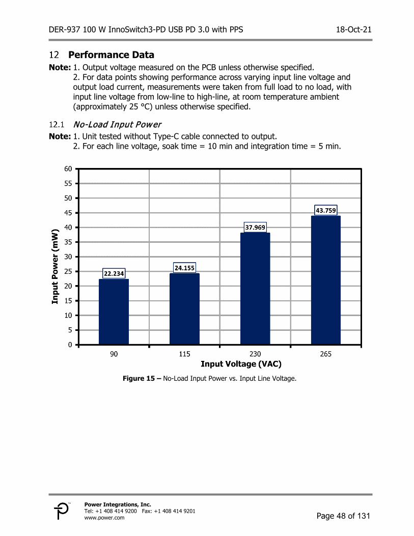
DER-937 100 W InnoSwitch3-PD USB PD 3.0 with PPS 18-Oct-21
Page 48 of 131
Power Integrations, Inc. Tel: +1 408 414 9200 Fax: +1 408 414 9201 www.power.com
Performance Data Note: 1. Output voltage measured on the PCB unless otherwise specified.
2. For data points showing performance across varying input line voltage and output load current, measurements were taken from full load to no load, with input line voltage from low-line to high-line, at room temperature ambient (approximately 25 °C) unless otherwise specified.
No-Load Input Power Note: 1. Unit tested without Type-C cable connected to output. 2. For each line voltage, soak time = 10 min and integration time = 5 min.
Figure 15 – No-Load Input Power vs. Input Line Voltage.

DER-937 100 W InnoSwitch3-PD USB PD 3.0 with PPS 18-Oct-21
Page 49 of 131
Power Integrations, Inc. Tel: +1 408 414 9200 Fax: +1 408 414 9201 www.power.com
Full Load Efficiency (On-board) VOUT (V)
Load (A)
Power (W)
Full Load Efficiency (%) 90 VAC 115 VAC 230 VAC 265 VAC
5 5.0 25 90.87 91.52 92.58 92.30 9 5.0 45 91.34 92.18 93.26 93.06 12 5.0 60 91.14 92.21 93.63 93.52 15 5.0 75 91.30 91.80 92.53 92.87 20 5.0 100 91.04 91.89 93.32 93.41
Average and 10% Load Efficiency Measurements were taken after 30-minute delay per input line voltage and 1-minute delay per load condition. Output voltage was measured on the board.
Efficiency Requirements
Test Average Efficiency (%)
10% Load Efficiency (%)
Effective 2016 Jan-16 Jan-16 VOUT (V)
Model (V)
Power (W)
New EISA2007
CoC v5 Tier 2 CoC v5 Tier 2
5 <6 25 84.25 85.00 73.18 9 >6 45 87.73 88.85 78.43 12 >6 60 88.00 89.00 79.00 15 >6 75 88.00 89.00 79.00 20 >6 100 88.00 89.00 79.00
Efficiency Performance Summary (On Board)
VOUT (V)
Power (W)
Average Efficiency (%)
10% Load Efficiency (%)
115 VAC 230 VAC 115 VAC 230 VAC 5 25 92.10 91.47 90.95 87.44 9 45 92.60 92.77 90.97 88.32 12 60 92.64 93.17 90.80 88.70 15 75 91.87 91.97 90.50 88.86 20 100 91.30 91.32 89.96 88.99

DER-937 100 W InnoSwitch3-PD USB PD 3.0 with PPS 18-Oct-21
Page 50 of 131
Power Integrations, Inc. Tel: +1 408 414 9200 Fax: +1 408 414 9201 www.power.com
Average and 10% Load Efficiency Measurements
Output: 5 V / 5 A
Input (VAC)
Load (%)
Design Performance Efficiency Standards
Remarks PIN (W)
VOUT (V)
IOUT (A)
POUT (W)
Efficiency (%)
Average Efficiency
(%)
DOE6 (%)
CoC v5 Tier 2 (%)
115
100 26.970 4.935 5.002 24.683 91.52
92.10 84.25 85.00 PASS 75 20.190 4.958 3.752 18.599 92.12 50 13.450 4.974 2.501 12.441 92.50 25 6.756 4.985 1.251 6.234 92.27 10 2.752 5.003 0.500 2.503 90.95 75.47 PASS
230
100 26.770 4.955 5.002 24.785 92.58
91.47 84.25 85.00 PASS 75 20.280 4.968 3.752 18.636 91.89 50 13.610 4.980 2.501 12.456 91.52 25 6.940 4.989 1.251 6.238 89.88 10 2.867 5.011 0.500 2.507 87.44 75.47 PASS
Output: 9 V / 5 A
Input (VAC)
Load (%)
Design Performance Efficiency Standards
Remarks PIN (W)
VOUT (V)
IOUT (A)
POUT (W)
Efficiency (%)
Average Efficiency
(%) DOE6 (%)
CoC v5 Tier 2 (%)
115
100 48.480 8.934 5.002 44.687 92.18
92.60 87.73 88.85 PASS 75 36.310 8.960 3.751 33.612 92.57 50 24.180 8.982 2.501 22.464 92.90 25 12.125 8.994 1.251 11.247 92.76 10 4.949 8.999 0.500 4.502 90.97 78.85 PASS
230
100 48.010 8.951 5.002 44.773 93.26
92.77 87.73 88.85 PASS 75 36.150 8.981 3.752 33.693 93.20 50 24.180 8.991 2.501 22.487 93.00 25 12.280 8.995 1.251 11.249 91.60 10 5.102 9.004 0.500 4.506 88.32 78.85 PASS

DER-937 100 W InnoSwitch3-PD USB PD 3.0 with PPS 18-Oct-21
Page 51 of 131
Power Integrations, Inc. Tel: +1 408 414 9200 Fax: +1 408 414 9201 www.power.com
Output: 12 V / 5 A
Input (VAC)
Load (%)
Design Performance Efficiency Standards
Remarks PIN (W)
VOUT (V)
IOUT (A)
POUT (W)
Efficiency (%)
Average Efficiency
(%) DOE6 (%)
CoC v5 Tier 2 (%)
115
100 64.680 11.926 5.001 59.643 92.21
92.64 88.00 89.00 PASS 75 48.340 11.953 3.751 44.837 92.75 50 32.250 11.974 2.501 29.941 92.84 25 16.160 11.989 1.250 14.989 92.75 10 6.601 11.989 0.500 5.994 90.80 79.00 PASS
230
100 63.800 11.944 5.001 59.733 93.63
93.17 88.00 89.00 PASS 75 48.030 11.978 3.751 44.930 93.55 50 32.100 11.986 2.501 29.971 93.37 25 16.270 11.991 1.250 14.991 92.14 10 6.760 11.993 0.500 5.996 88.70 79.00 PASS
Output: 15 V / 5 A
Input (VAC)
Load (%)
Design Performance Efficiency Standards
Remarks PIN (W)
VOUT (V)
IOUT (A)
POUT (W)
Efficiency (%)
Average Efficiency
(%) DOE6 (%)
CoC v5 Tier 2 (%)
115
100 81.400 14.942 5.001 74.723 91.80
91.87 88.00 89.00 PASS 75 61.310 14.983 3.751 56.200 91.67 50 41.050 14.988 2.501 37.477 91.30 25 20.210 14.988 1.250 18.737 92.71 10 8.284 14.994 0.500 7.497 90.50 79.00 PASS
230
100 80.760 14.943 5.001 74.730 92.53
91.97 88.00 89.00 PASS 75 61.100 14.984 3.751 56.205 91.99 50 41.210 14.989 2.501 37.481 90.95 25 20.280 14.994 1.250 18.744 92.43 10 8.440 15.000 0.500 7.500 88.86 79.00 PASS

DER-937 100 W InnoSwitch3-PD USB PD 3.0 with PPS 18-Oct-21
Page 52 of 131
Power Integrations, Inc. Tel: +1 408 414 9200 Fax: +1 408 414 9201 www.power.com
Output: 20 V / 5 A
Input (VAC)
Load (%)
Design Performance Efficiency Standards
Remarks PIN (W)
VOUT (V)
IOUT (A)
POUT (W)
Efficiency (%)
Average Efficiency
(%) DOE6 (%)
CoC v5 Tier 2 (%)
115
100 108.490 19.935 5.001 99.690 91.89
91.30 88.00 89.00 PASS 75 81.630 19.964 3.751 74.880 91.73 50 54.560 19.969 2.500 49.930 91.51 25 27.725 19.973 1.250 24.968 90.06 10 11.096 19.967 0.500 9.982 89.96 79.00 PASS
230
100 106.800 19.930 5.001 99.670 93.32
91.32 88.00 89.00 PASS 75 80.950 19.958 3.751 74.850 92.46 50 54.510 19.967 2.500 49.920 91.58 25 28.400 19.971 1.250 24.966 87.91 10 11.220 19.971 0.500 9.985 88.99 79.00 PASS
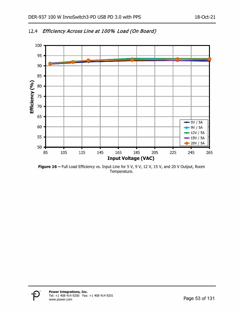
DER-937 100 W InnoSwitch3-PD USB PD 3.0 with PPS 18-Oct-21
Page 53 of 131
Power Integrations, Inc. Tel: +1 408 414 9200 Fax: +1 408 414 9201 www.power.com
Efficiency Across Line at 100% Load (On Board)
Figure 16 – Full Load Efficiency vs. Input Line for 5 V, 9 V, 12 V, 15 V, and 20 V Output, Room
Temperature.

DER-937 100 W InnoSwitch3-PD USB PD 3.0 with PPS 18-Oct-21
Page 54 of 131
Power Integrations, Inc. Tel: +1 408 414 9200 Fax: +1 408 414 9201 www.power.com
Efficiency Across Load (On Board) Note: 1. The PFC bias circuit has been configured to operate as discussed in Section 4.2.
Improvement in efficiency is expected for operating conditions wherein the PFC stage is disabled.
Output: 5 V / 5 A
Figure 17 – Efficiency vs. Load for 5 V Output, Room Temperature.
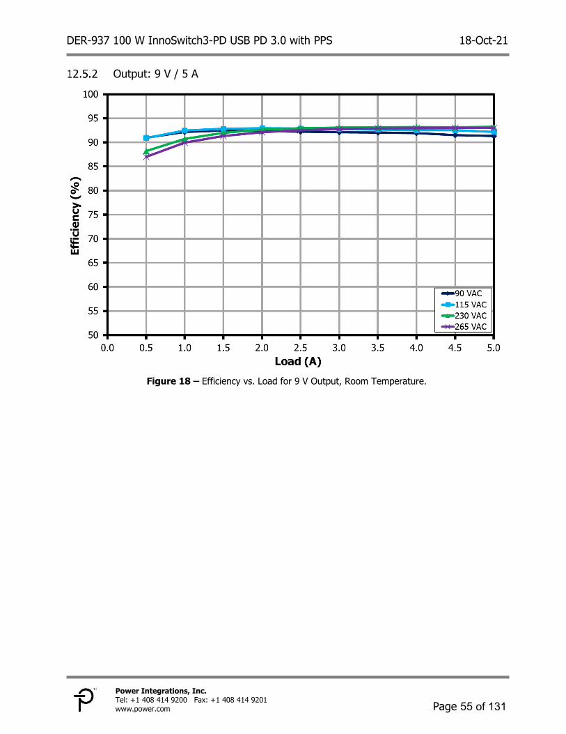
DER-937 100 W InnoSwitch3-PD USB PD 3.0 with PPS 18-Oct-21
Page 55 of 131
Power Integrations, Inc. Tel: +1 408 414 9200 Fax: +1 408 414 9201 www.power.com
Output: 9 V / 5 A
Figure 18 – Efficiency vs. Load for 9 V Output, Room Temperature.

DER-937 100 W InnoSwitch3-PD USB PD 3.0 with PPS 18-Oct-21
Page 56 of 131
Power Integrations, Inc. Tel: +1 408 414 9200 Fax: +1 408 414 9201 www.power.com
Output: 12 V / 5 A
Figure 19 – Efficiency vs. Load for 12 V Output, Room Temperature.
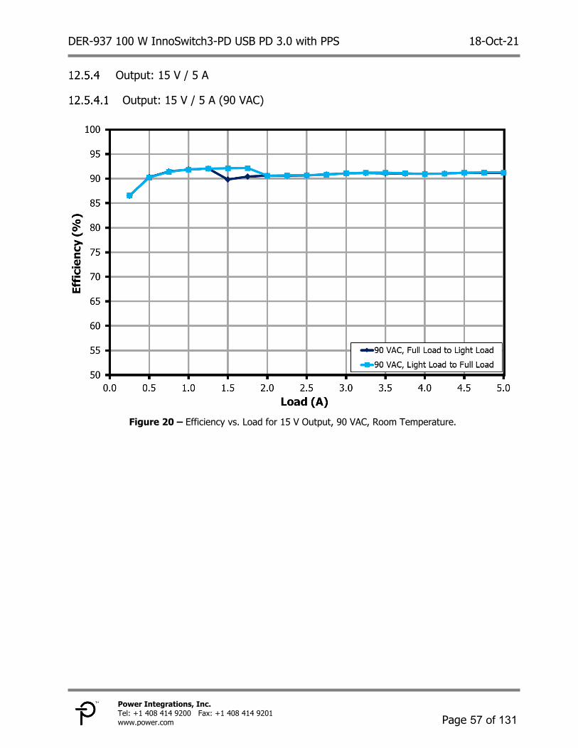
DER-937 100 W InnoSwitch3-PD USB PD 3.0 with PPS 18-Oct-21
Page 57 of 131
Power Integrations, Inc. Tel: +1 408 414 9200 Fax: +1 408 414 9201 www.power.com
Output: 15 V / 5 A
Output: 15 V / 5 A (90 VAC)
Figure 20 – Efficiency vs. Load for 15 V Output, 90 VAC, Room Temperature.
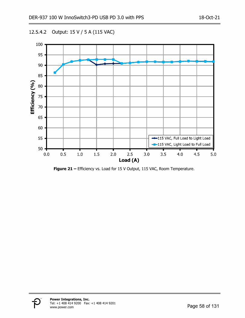
DER-937 100 W InnoSwitch3-PD USB PD 3.0 with PPS 18-Oct-21
Page 58 of 131
Power Integrations, Inc. Tel: +1 408 414 9200 Fax: +1 408 414 9201 www.power.com
Output: 15 V / 5 A (115 VAC)
Figure 21 – Efficiency vs. Load for 15 V Output, 115 VAC, Room Temperature.
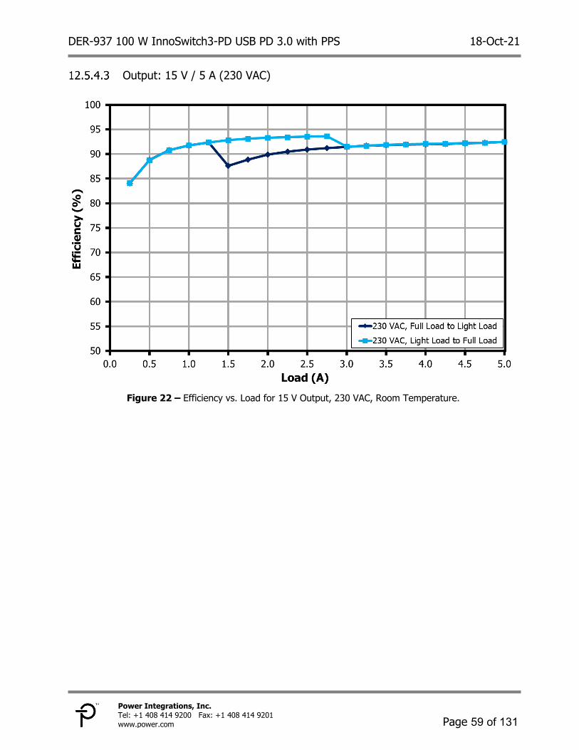
DER-937 100 W InnoSwitch3-PD USB PD 3.0 with PPS 18-Oct-21
Page 59 of 131
Power Integrations, Inc. Tel: +1 408 414 9200 Fax: +1 408 414 9201 www.power.com
Output: 15 V / 5 A (230 VAC)
Figure 22 – Efficiency vs. Load for 15 V Output, 230 VAC, Room Temperature.

DER-937 100 W InnoSwitch3-PD USB PD 3.0 with PPS 18-Oct-21
Page 60 of 131
Power Integrations, Inc. Tel: +1 408 414 9200 Fax: +1 408 414 9201 www.power.com
Output: 15 V / 5 A (265 VAC)
Figure 23 – Efficiency vs. Load for 15 V Output, 265 VAC, Room Temperature.

DER-937 100 W InnoSwitch3-PD USB PD 3.0 with PPS 18-Oct-21
Page 61 of 131
Power Integrations, Inc. Tel: +1 408 414 9200 Fax: +1 408 414 9201 www.power.com
Output: 20 V / 5 A
Output: 20 V / 5 A (90 VAC)
Figure 24 – Efficiency vs. Load for 20 V Output, 90 VAC, Room Temperature.

DER-937 100 W InnoSwitch3-PD USB PD 3.0 with PPS 18-Oct-21
Page 62 of 131
Power Integrations, Inc. Tel: +1 408 414 9200 Fax: +1 408 414 9201 www.power.com
Output: 20 V / 5 A (115 VAC)
Figure 25 – Efficiency vs. Load for 20 V Output, 115 VAC, Room Temperature.
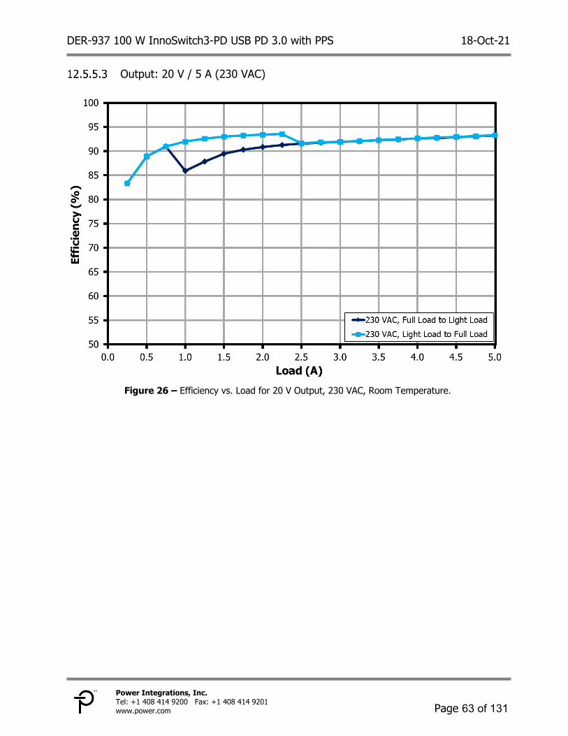
DER-937 100 W InnoSwitch3-PD USB PD 3.0 with PPS 18-Oct-21
Page 63 of 131
Power Integrations, Inc. Tel: +1 408 414 9200 Fax: +1 408 414 9201 www.power.com
Output: 20 V / 5 A (230 VAC)
Figure 26 – Efficiency vs. Load for 20 V Output, 230 VAC, Room Temperature.

DER-937 100 W InnoSwitch3-PD USB PD 3.0 with PPS 18-Oct-21
Page 64 of 131
Power Integrations, Inc. Tel: +1 408 414 9200 Fax: +1 408 414 9201 www.power.com
Output: 20 V / 5 A (265 VAC)
Figure 27 – Efficiency vs. Load for 20 V Output, 265 VAC, Room Temperature.
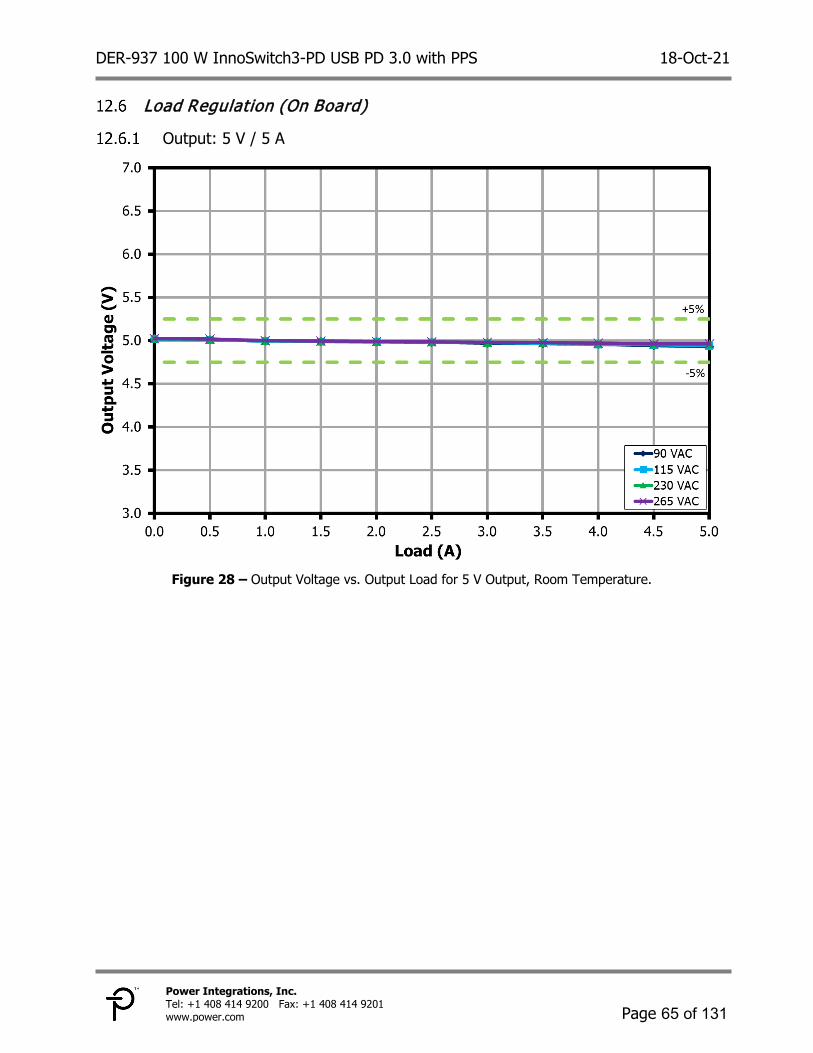
DER-937 100 W InnoSwitch3-PD USB PD 3.0 with PPS 18-Oct-21
Page 65 of 131
Power Integrations, Inc. Tel: +1 408 414 9200 Fax: +1 408 414 9201 www.power.com
Load Regulation (On Board)
Output: 5 V / 5 A
Figure 28 – Output Voltage vs. Output Load for 5 V Output, Room Temperature.

DER-937 100 W InnoSwitch3-PD USB PD 3.0 with PPS 18-Oct-21
Page 66 of 131
Power Integrations, Inc. Tel: +1 408 414 9200 Fax: +1 408 414 9201 www.power.com
Output: 9 V / 5 A
Figure 29 – Output Voltage vs. Output Load for 9 V Output, Room Temperature.

DER-937 100 W InnoSwitch3-PD USB PD 3.0 with PPS 18-Oct-21
Page 67 of 131
Power Integrations, Inc. Tel: +1 408 414 9200 Fax: +1 408 414 9201 www.power.com
Output: 12 V / 5 A
Figure 30 – Output Voltage vs. Output Load for 12 V Output, Room Temperature.

DER-937 100 W InnoSwitch3-PD USB PD 3.0 with PPS 18-Oct-21
Page 68 of 131
Power Integrations, Inc. Tel: +1 408 414 9200 Fax: +1 408 414 9201 www.power.com
Output: 15 V / 5 A
Figure 31 – Output Voltage vs. Output Load for 15 V Output, Room Temperature.
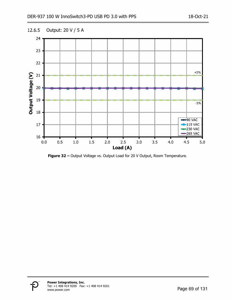
DER-937 100 W InnoSwitch3-PD USB PD 3.0 with PPS 18-Oct-21
Page 69 of 131
Power Integrations, Inc. Tel: +1 408 414 9200 Fax: +1 408 414 9201 www.power.com
Output: 20 V / 5 A
Figure 32 – Output Voltage vs. Output Load for 20 V Output, Room Temperature.

DER-937 100 W InnoSwitch3-PD USB PD 3.0 with PPS 18-Oct-21
Page 70 of 131
Power Integrations, Inc. Tel: +1 408 414 9200 Fax: +1 408 414 9201 www.power.com
Line Regulation (On Board)
Output: 5 V / 5 A
Figure 33 – Output Voltage vs. Input Line Voltage for 5 V Output, Room Temperature.
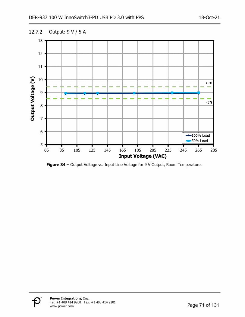
DER-937 100 W InnoSwitch3-PD USB PD 3.0 with PPS 18-Oct-21
Page 71 of 131
Power Integrations, Inc. Tel: +1 408 414 9200 Fax: +1 408 414 9201 www.power.com
Output: 9 V / 5 A
Figure 34 – Output Voltage vs. Input Line Voltage for 9 V Output, Room Temperature.

DER-937 100 W InnoSwitch3-PD USB PD 3.0 with PPS 18-Oct-21
Page 72 of 131
Power Integrations, Inc. Tel: +1 408 414 9200 Fax: +1 408 414 9201 www.power.com
Output: 12 V / 5 A
Figure 35 – Output Voltage vs. Input Line Voltage for 12 V Output, Room Temperature.
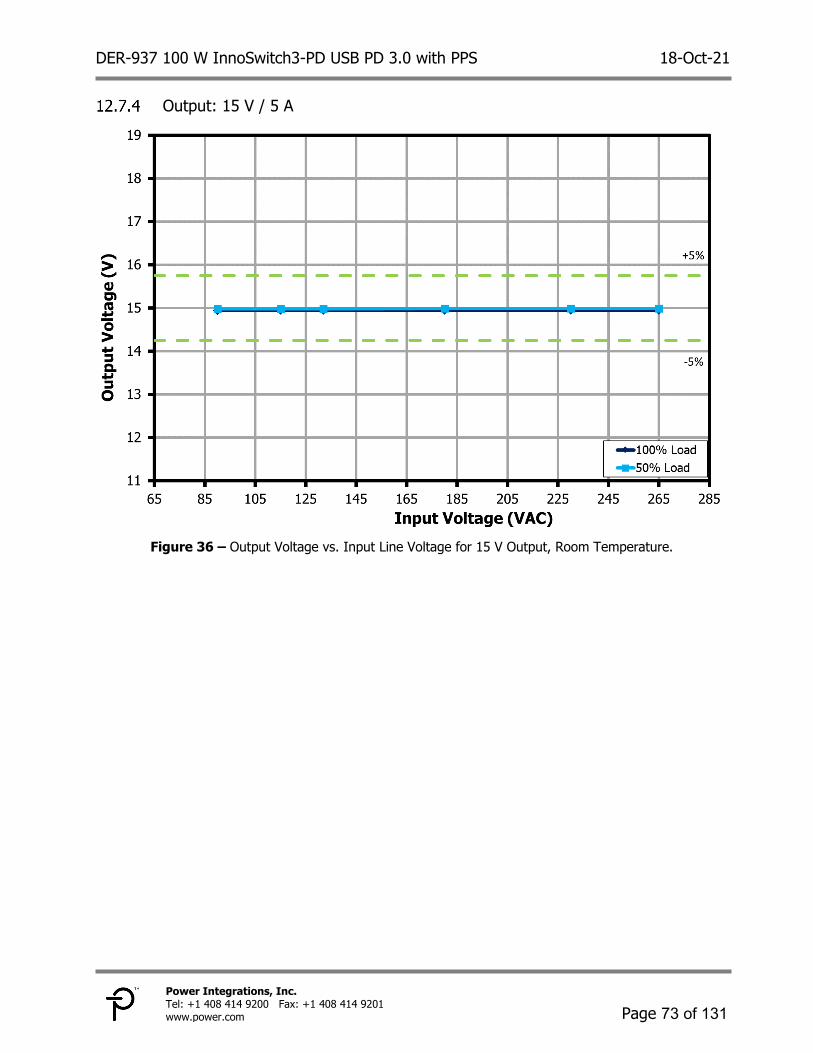
DER-937 100 W InnoSwitch3-PD USB PD 3.0 with PPS 18-Oct-21
Page 73 of 131
Power Integrations, Inc. Tel: +1 408 414 9200 Fax: +1 408 414 9201 www.power.com
Output: 15 V / 5 A
Figure 36 – Output Voltage vs. Input Line Voltage for 15 V Output, Room Temperature.

DER-937 100 W InnoSwitch3-PD USB PD 3.0 with PPS 18-Oct-21
Page 74 of 131
Power Integrations, Inc. Tel: +1 408 414 9200 Fax: +1 408 414 9201 www.power.com
Output: 20 V / 5 A
Figure 37 – Output Voltage vs. Input Line Voltage for 20 V Output, Room Temperature.

DER-937 100 W InnoSwitch3-PD USB PD 3.0 with PPS 18-Oct-21
Page 75 of 131
Power Integrations, Inc. Tel: +1 408 414 9200 Fax: +1 408 414 9201 www.power.com
Input Current Harmonics
Output: 15 V / 5 A (115 VAC) Input Input Measurement Output Measurement
VAC(RMS) Freq (Hz) VIN(RMS) IIN
(mA) PIN (W) PF %
THD VOUT (V)
IOUT (mA)
POUT (W)
%V Reg
Efficiency (%)
115 60 114.85 728.60 81.34 0.97 18.05 14.93 5001.10 74.69 0.44 91.82
Harmonic Order
Harmonic Content (mA)
Class D Limit (mA/W)
Class D Limit (mA) Remarks
1 709.5 3 115.5 3.40 276.59 Pass 5 44.3 1.90 154.57 Pass 7 21.0 1.00 81.35 Pass 9 12.8 0.50 40.68 Pass 11 12.4 0.35 28.47 Pass 13 3.7 0.30 24.09 Pass 15 3.5 0.26 20.88 Pass 17 5.9 0.23 18.42 Pass 19 8.1 0.20 16.48 Pass 21 8.8 0.18 14.91 Pass 23 8.8 0.17 13.62 Pass 25 8.9 0.15 12.53 Pass 27 6.1 0.14 11.60 Pass 31 5.9 0.12 10.10 Pass 31 5.9 0.12 10.10 Pass 33 3.4 0.12 9.49 Pass 35 4.9 0.11 8.95 Pass 37 4.1 0.10 8.46 Pass 39 2.5 0.10 8.03 Pass
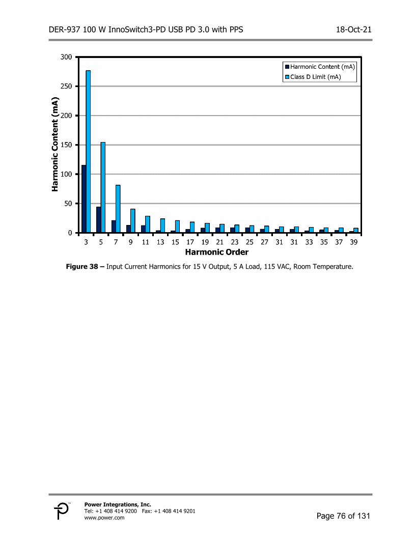
DER-937 100 W InnoSwitch3-PD USB PD 3.0 with PPS 18-Oct-21
Page 76 of 131
Power Integrations, Inc. Tel: +1 408 414 9200 Fax: +1 408 414 9201 www.power.com
Figure 38 – Input Current Harmonics for 15 V Output, 5 A Load, 115 VAC, Room Temperature.
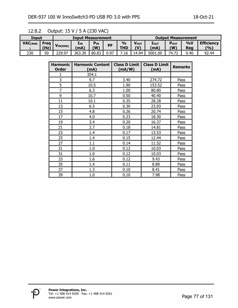
DER-937 100 W InnoSwitch3-PD USB PD 3.0 with PPS 18-Oct-21
Page 77 of 131
Power Integrations, Inc. Tel: +1 408 414 9200 Fax: +1 408 414 9201 www.power.com
Output: 15 V / 5 A (230 VAC) Input Input Measurement Output Measurement
VAC(RMS
) Freq (Hz) VIN(RMS) IIN
(mA) PIN (W) PF %
THD VOUT (V)
IOUT (mA)
POUT (W)
%V Reg
Efficiency (%)
230 50 229.97 363.30 80.83 0.97 7.16 14.94 5001.00 74.72 0.40 92.44
Harmonic Order
Harmonic Content (mA)
Class D Limit (mA/W)
Class D Limit (mA) Remarks
1 354.1 3 9.7 3.40 274.72 Pass 5 10.5 1.90 153.52 Pass 7 6.3 1.00 80.80 Pass 9 10.7 0.50 40.40 Pass 11 10.1 0.35 28.28 Pass 13 6.5 0.30 23.93 Pass 15 4.8 0.26 20.74 Pass 17 4.0 0.23 18.30 Pass 19 3.4 0.20 16.37 Pass 21 2.7 0.18 14.81 Pass 23 1.4 0.17 13.53 Pass 25 1.4 0.15 12.44 Pass 27 1.1 0.14 11.52 Pass 31 1.0 0.12 10.03 Pass 31 1.0 0.12 10.03 Pass 33 1.6 0.12 9.43 Pass 35 1.4 0.11 8.89 Pass 37 1.3 0.10 8.41 Pass 39 1.0 0.10 7.98 Pass

DER-937 100 W InnoSwitch3-PD USB PD 3.0 with PPS 18-Oct-21
Page 78 of 131
Power Integrations, Inc. Tel: +1 408 414 9200 Fax: +1 408 414 9201 www.power.com
Figure 39 – Input Current Harmonics for 15 V Output, 5 A Load, 230 VAC, Room Temperature.

DER-937 100 W InnoSwitch3-PD USB PD 3.0 with PPS 18-Oct-21
Page 79 of 131
Power Integrations, Inc. Tel: +1 408 414 9200 Fax: +1 408 414 9201 www.power.com
Output: 20 V / 5 A (115 VAC) Input Input Measurement Output Measurement
VAC(RMS) Freq (Hz) VIN(RMS) IIN
(mA) PIN (W) PF %
THD VOUT (V)
IOUT (mA)
POUT (W)
%V Reg
Efficiency (%)
115 60 114.82 961.40 108.41 0.98 14.84 19.93 5000.80 99.64 0.37 91.91
Harmonic Order
Harmonic Content (mA)
Class D Limit (mA/W)
Class D Limit (mA) Remarks
1 947.3 3 122.1 3.40 368.70 Pass 5 57.8 1.90 206.04 Pass 7 23.6 1.00 108.44 Pass 9 7.8 0.50 54.22 Pass 11 2.0 0.35 37.95 Pass 13 7.0 0.30 32.11 Pass 15 8.2 0.26 27.83 Pass 17 9.8 0.23 24.56 Pass 19 10.6 0.20 21.97 Pass 21 10.1 0.18 19.88 Pass 23 8.4 0.17 18.15 Pass 25 8.1 0.15 16.70 Pass 27 9.1 0.14 15.46 Pass 31 6.7 0.12 13.47 Pass 31 6.7 0.12 13.47 Pass 33 4.1 0.12 12.65 Pass 35 3.2 0.11 11.93 Pass 37 3.4 0.10 11.28 Pass 39 2.8 0.10 10.70 Pass

DER-937 100 W InnoSwitch3-PD USB PD 3.0 with PPS 18-Oct-21
Page 80 of 131
Power Integrations, Inc. Tel: +1 408 414 9200 Fax: +1 408 414 9201 www.power.com
Figure 40 – Input Current Harmonics for 20 V Output, 5 A Load, 115 VAC, Room Temperature.

DER-937 100 W InnoSwitch3-PD USB PD 3.0 with PPS 18-Oct-21
Page 81 of 131
Power Integrations, Inc. Tel: +1 408 414 9200 Fax: +1 408 414 9201 www.power.com
Output: 20 V / 5 A (230 VAC)
Input Input Measurement Output Measurement
VAC(RMS) Freq (Hz) VIN(RMS) IIN
(mA) PIN (W) PF %
THD VOUT (V)
IOUT (mA)
POUT (W)
%V Reg
Efficiency (%)
230 50 229.95 472.60 106.83 0.98 7.73 19.92 5001.00 99.64 0.38 93.27
Harmonic Order
Harmonic Content (mA)
Class D Limit (mA/W)
Class D Limit (mA) Remarks
1 467.5 3 30.6 3.40 363.22 Pass 5 14.8 1.90 202.98 Pass 7 4.8 1.00 106.83 Pass 9 0.2 0.50 53.42 Pass 11 1.5 0.35 37.39 Pass 13 1.4 0.30 31.64 Pass 15 1.3 0.26 27.42 Pass 17 2.7 0.23 24.19 Pass 19 1.2 0.20 21.65 Pass 21 2.5 0.18 19.59 Pass 23 1.3 0.17 17.88 Pass 25 2.2 0.15 16.45 Pass 27 2.0 0.14 15.23 Pass 31 3.1 0.12 13.27 Pass 31 3.1 0.12 13.27 Pass 33 0.8 0.12 12.46 Pass 35 2.4 0.11 11.75 Pass 37 1.5 0.10 11.12 Pass 39 1.3 0.10 10.55 Pass

DER-937 100 W InnoSwitch3-PD USB PD 3.0 with PPS 18-Oct-21
Page 82 of 131
Power Integrations, Inc. Tel: +1 408 414 9200 Fax: +1 408 414 9201 www.power.com
Figure 41 – Input Current Harmonics for 20 V Output, 5 A Load, 230 VAC, Room Temperature.

DER-937 100 W InnoSwitch3-PD USB PD 3.0 with PPS 18-Oct-21
Page 83 of 131
Power Integrations, Inc. Tel: +1 408 414 9200 Fax: +1 408 414 9201 www.power.com
Thermal Performance
Thermal Performance in Open Case, Room Temperature Note: 1. Open case thermal images are taken at room temperature ambient with the
unit inside a closed acrylic box and 1-hour soak per condition. 2. For enclosed adapter application, this design requires use of metallic heat
spreader and suitable thermally conductive insulator pads to ensure low temperature of the bridge rectifiers, HiperPFS-4, and InnoSwitch3-PD IC. The performance data below is for open case operation and does not use heat spreader for cooling.
Output: 5 V / 5 A (90 VAC)
Figure 42 – Bottom Thermal Image, TAMB = 27.4 ºC.
Bx1: InnoSwitch3-PD = 52.8 ºC. Bx2: Primary Clamp = 50.9 ºC. Bx3: SR FET = 54.0 ºC. Bx4: SR FET Snubber = 54.3 ºC. Bx5: HiperPFS-4 = 42.4 ºC. Bx6: PFC Boost Diode = 43.9 ºC. Bx7: Bridge Rectifier = 49.0 ºC.
Figure 43 – Top Thermal Image, TAMB = 27.4 ºC. Bx1: Transformer Core = 50.4 ºC. Bx2: Transformer Wire = 53.5 ºC. Bx3: PFC Inductor Core = 40.5 ºC. Bx4: Boost Pre-charge Diode = 47.4 ºC.
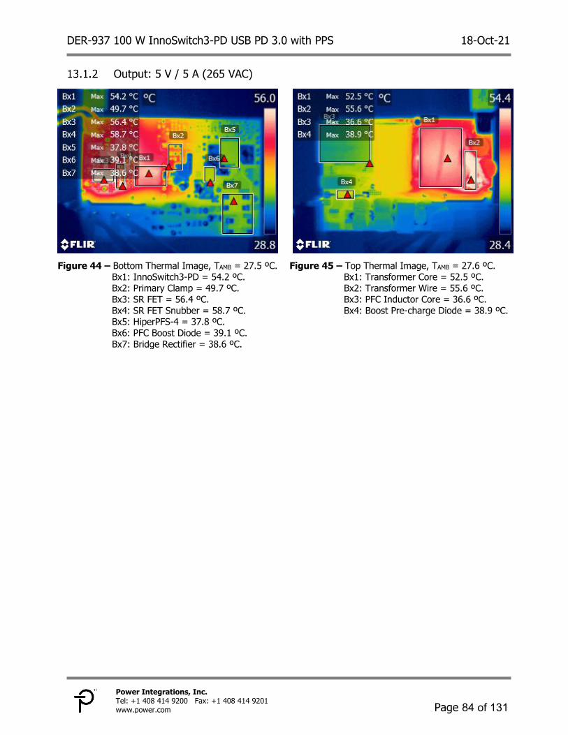
DER-937 100 W InnoSwitch3-PD USB PD 3.0 with PPS 18-Oct-21
Page 84 of 131
Power Integrations, Inc. Tel: +1 408 414 9200 Fax: +1 408 414 9201 www.power.com
Output: 5 V / 5 A (265 VAC)
Figure 44 – Bottom Thermal Image, TAMB = 27.5 ºC.
Bx1: InnoSwitch3-PD = 54.2 ºC. Bx2: Primary Clamp = 49.7 ºC. Bx3: SR FET = 56.4 ºC. Bx4: SR FET Snubber = 58.7 ºC. Bx5: HiperPFS-4 = 37.8 ºC. Bx6: PFC Boost Diode = 39.1 ºC. Bx7: Bridge Rectifier = 38.6 ºC.
Figure 45 – Top Thermal Image, TAMB = 27.6 ºC. Bx1: Transformer Core = 52.5 ºC. Bx2: Transformer Wire = 55.6 ºC. Bx3: PFC Inductor Core = 36.6 ºC. Bx4: Boost Pre-charge Diode = 38.9 ºC.

DER-937 100 W InnoSwitch3-PD USB PD 3.0 with PPS 18-Oct-21
Page 85 of 131
Power Integrations, Inc. Tel: +1 408 414 9200 Fax: +1 408 414 9201 www.power.com
Output: 9 V / 5 A (90 VAC)
Figure 46 – Bottom Thermal Image, TAMB = 28.4 ºC.
Bx1: InnoSwitch3-PD = 70.6 ºC. Bx2: Primary Clamp = 66.7 ºC. Bx3: SR FET = 65.4 ºC. Bx4: SR FET Snubber = 66.9 ºC. Bx5: HiperPFS-4 = 53.4 ºC. Bx6: PFC Boost Diode = 55.9 ºC. Bx7: Bridge Rectifier = 66.0 ºC.
Figure 47 – Top Thermal Image, TAMB = 28.3 ºC. Bx1: Transformer Core = 62.8 ºC. Bx2: Transformer Wire = 66.2 ºC. Bx3: PFC Inductor Core = 50.2 ºC. Bx4: Boost Pre-charge Diode = 62.9 ºC.
Output: 9 V / 5 A (265 VAC)
Figure 48 – Bottom Thermal Image, TAMB = 27.8 ºC.
Bx1: InnoSwitch3-PD = 66.3 ºC. Bx2: Primary Clamp = 59.7 ºC. Bx3: SR FET = 65.4 ºC. Bx4: SR FET Snubber = 68.7 ºC. Bx5: HiperPFS-4 = 42.5 ºC. Bx6: PFC Boost Diode = 44.5 ºC. Bx7: Bridge Rectifier = 44.9 ºC.
Figure 49 – Top Thermal Image, TAMB = 27.8 ºC. Bx1: Transformer Core = 63.6 ºC. Bx2: Transformer Wire = 66.6 ºC. Bx3: PFC Inductor Core = 41.2 ºC. Bx4: Boost Pre-charge Diode = 45.3 ºC.

DER-937 100 W InnoSwitch3-PD USB PD 3.0 with PPS 18-Oct-21
Page 86 of 131
Power Integrations, Inc. Tel: +1 408 414 9200 Fax: +1 408 414 9201 www.power.com
Output: 12 V / 5 A (90 VAC)
Figure 50 – Bottom Thermal Image, TAMB = 28.2 ºC.
Bx1: InnoSwitch3-PD = 86.6 ºC. Bx2: Primary Clamp = 79.0 ºC. Bx3: SR FET = 74.4 ºC. Bx4: SR FET Snubber = 77.8 ºC. Bx5: HiperPFS-4 = 60.7 ºC. Bx6: PFC Boost Diode = 64.6 ºC. Bx7: Bridge Rectifier = 78.8 ºC.
Figure 51 – Top Thermal Image, TAMB = 28.2 ºC. Bx1: Transformer Core = 70.8 ºC. Bx2: Transformer Wire = 74.8 ºC. Bx3: PFC Inductor Core = 57.0 ºC. Bx4: Boost Pre-charge Diode = 74.2 ºC.
Output: 12 V / 5 A (265 VAC)
Figure 52 – Bottom Thermal Image, TAMB = 28.2 ºC.
Bx1: InnoSwitch3-PD = 74.1 ºC. Bx2: Primary Clamp = 66.8 ºC. Bx3: SR FET = 71.4 ºC. Bx4: SR FET Snubber = 74.8 ºC. Bx5: HiperPFS-4 = 46.1 ºC. Bx6: PFC Boost Diode = 48.5 ºC. Bx7: Bridge Rectifier = 49.8 ºC.
Figure 53 – Top Thermal Image, TAMB = 28.2 ºC. Bx1: Transformer Core = 72.1 ºC. Bx2: Transformer Wire = 74.4 ºC. Bx3: PFC Inductor Core = 45.6 ºC. Bx4: Boost Pre-charge Diode = 51.1 ºC.

DER-937 100 W InnoSwitch3-PD USB PD 3.0 with PPS 18-Oct-21
Page 87 of 131
Power Integrations, Inc. Tel: +1 408 414 9200 Fax: +1 408 414 9201 www.power.com
Output: 15 V / 5 A (90 VAC)
Figure 54 – Bottom Thermal Image, TAMB = 28.0 ºC.
Bx1: InnoSwitch3-PD = 88.6 ºC. Bx2: Primary Clamp = 82.8 ºC. Bx3: SR FET = 79.5 ºC. Bx4: SR FET Snubber = 82.8 ºC. Bx5: HiperPFS-4 = 79.4 ºC. Bx6: PFC Boost Diode = 78.0 ºC. Bx7: Bridge Rectifier = 84.6 ºC.
Figure 55 – Top Thermal Image, TAMB = 28.3 ºC. Bx1: Transformer Core = 82.0 ºC. Bx2: Transformer Wire = 84.4 ºC. Bx3: PFC Inductor Core = 70.9 ºC. Bx4: Boost Pre-charge Diode = 73.5 ºC.
Output: 15 V / 5 A (265 VAC)
Figure 56 – Bottom Thermal Image, TAMB = 28.9 ºC.
Bx1: InnoSwitch3-PD = 85.1 ºC. Bx2: Primary Clamp = 79.3 ºC. Bx3: SR FET = 78.7 ºC. Bx4: SR FET Snubber = 81.8 ºC. Bx5: HiperPFS-4 = 76.2 ºC. Bx6: PFC Boost Diode = 70.3 ºC. Bx7: Bridge Rectifier = 59.1 ºC.
Figure 57 – Top Thermal Image, TAMB = 28.8 ºC. Bx1: Transformer Core = 80.6 ºC. Bx2: Transformer Wire = 82.5 ºC. Bx3: PFC Inductor Core = 59.2 ºC. Bx4: Boost Pre-charge Diode = 59.1 ºC.

DER-937 100 W InnoSwitch3-PD USB PD 3.0 with PPS 18-Oct-21
Page 88 of 131
Power Integrations, Inc. Tel: +1 408 414 9200 Fax: +1 408 414 9201 www.power.com
Output: 20 V / 5 A (90 VAC)
Figure 58 – Bottom Thermal Image, TAMB = 27.9 ºC.
Bx1: InnoSwitch3-PD = 103.4 ºC. Bx2: Primary Clamp = 96.4 ºC. Bx3: SR FET = 88.0 ºC. Bx4: SR FET Snubber = 91.1 ºC. Bx5: HiperPFS-4 = 110.6 ºC. Bx6: PFC Boost Diode = 100.6 ºC. Bx7: Bridge Rectifier = 103.2 ºC.
Figure 59 – Top Thermal Image, TAMB = 27.9 ºC. Bx1: Transformer Core = 94.3 ºC. Bx2: Transformer Wire = 95.4 ºC. Bx3: PFC Inductor Core = 88.5 ºC. Bx4: Boost Pre-charge Diode = 88.2 ºC.
Output: 20 V / 5 A (265 VAC)
Figure 60 – Bottom Thermal Image, TAMB = 27.5 ºC.
Bx1: InnoSwitch3-PD = 94.2 ºC. Bx2: Primary Clamp = 86.7 ºC. Bx3: SR FET = 84.6 ºC. Bx4: SR FET Snubber = 87.7 ºC. Bx5: HiperPFS-4 = 81.3 ºC. Bx6: PFC Boost Diode = 75.7 ºC. Bx7: Bridge Rectifier = 63.1 ºC.
Figure 61 – Top Thermal Image, TAMB = 27.4 ºC. Bx1: Transformer Core = 90.0 ºC. Bx2: Transformer Wire = 91.0 ºC. Bx3: PFC Inductor Core = 61.7 ºC. Bx4: Boost Pre-charge Diode = 62.5 ºC.

DER-937 100 W InnoSwitch3-PD USB PD 3.0 with PPS 18-Oct-21
Page 89 of 131
Power Integrations, Inc. Tel: +1 408 414 9200 Fax: +1 408 414 9201 www.power.com
Waveforms Note: 1. Output voltage captured at the end of 100 mΩ cable unless otherwise specified.
2. Waveforms taken at room temperature ambient (approximately 25 °C).
Input Voltage and Current Waveforms
Output: 15 V / 5 A
Figure 62 – Input Voltage and Current.
115 VAC, 15.0 V, 5 A Load. CH1: VIN_AC, 100 V / div. CH2: IIN_AC, 1 A / div. Time: 4 ms / div.
Figure 63 – Input Drain Voltage and Current. 230 VAC, 15.0 V, 5 A Load. CH1: VIN_AC, 100 V / div. CH2: IIN_AC, 1 A / div. Time: 4 ms / div.
Output: 20 V / 5 A
Figure 64 – Input Drain Voltage and Current.
90 VAC, 20.0 V, 5 A Load. CH1: VIN_AC, 100 V / div. CH2: IIN_AC, 1 A / div. Time: 4 ms / div.
Figure 65 – Input Drain Voltage and Current. 265 VAC, 20.0 V, 5 A Load. CH1: VIN_AC, 100 V / div. CH2: IIN_AC, 1 A / div. Time: 4 ms / div.

DER-937 100 W InnoSwitch3-PD USB PD 3.0 with PPS 18-Oct-21
Page 90 of 131
Power Integrations, Inc. Tel: +1 408 414 9200 Fax: +1 408 414 9201 www.power.com
PFC Inductor Current and HiperPFS-4 Drain Voltage Waveforms
Output: 15 V / 5 A
Figure 66 – PFC Inductor Current and HiperPFS-4
Drain Voltage. 115 VAC, 15.0 V, 5 A Load. VDS_PFS = 414 V Maximum. IL_PFC = 2.60 A Maximum. CH1: VDS_PFS, 100 V / div. CH2: IL_PFC, 500 mA / div. Time: 4 ms / div. (25 µs / div. Zoom).
Figure 67 – PFC Inductor Current and HiperPFS-4 Drain Voltage. 230 VAC, 15.0 V, 5 A Load. VDS_PFS = 406 V Maximum. IL_PFC = 1.36 A Maximum. CH1: VDS_PFS, 100 V / div. CH2: IL_PFC, 500 mA / div. Time: 4 ms / div. (25 µs / div. Zoom).
Output: 20 V / 5 A
Figure 68 – PFC Inductor Current and HiperPFS-4
Drain Voltage. 115 VAC, 20.0 V, 5 A Load. VDS_PFS = 418 V Maximum. IL_PFC = 2.96 A Maximum. CH1: VDS_PFS, 100 V / div. CH2: IL_PFC, 500 mA / div. Time: 4 ms / div. (25 µs / div. Zoom).
Figure 69 – PFC Inductor Current and HiperPFS-4 Drain Voltage. 230 VAC, 20.0 V, 5 A Load. VDS_PFS = 406 V Maximum. IL_PFC = 1.539 A Maximum. CH1: VDS_PFS, 100 V / div. CH2: IL_PFC, 500 mA / div. Time: 4 ms / div. (25 µs / div. Zoom).
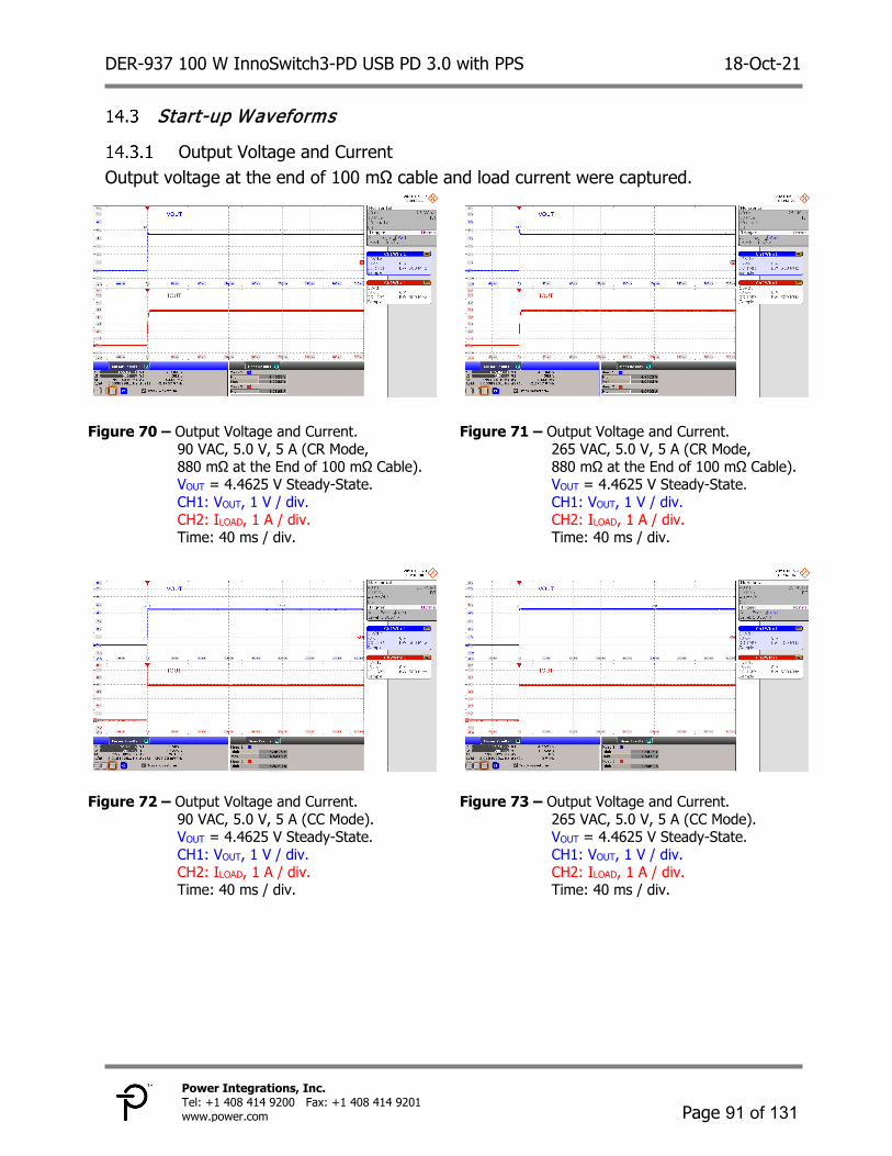
DER-937 100 W InnoSwitch3-PD USB PD 3.0 with PPS 18-Oct-21
Page 91 of 131
Power Integrations, Inc. Tel: +1 408 414 9200 Fax: +1 408 414 9201 www.power.com
Start-up Waveforms
Output Voltage and Current Output voltage at the end of 100 mΩ cable and load current were captured.
Figure 70 – Output Voltage and Current.
90 VAC, 5.0 V, 5 A (CR Mode, 880 mΩ at the End of 100 mΩ Cable). VOUT = 4.4625 V Steady-State. CH1: VOUT, 1 V / div. CH2: ILOAD, 1 A / div. Time: 40 ms / div.
Figure 71 – Output Voltage and Current. 265 VAC, 5.0 V, 5 A (CR Mode, 880 mΩ at the End of 100 mΩ Cable). VOUT = 4.4625 V Steady-State. CH1: VOUT, 1 V / div. CH2: ILOAD, 1 A / div. Time: 40 ms / div.
Figure 72 – Output Voltage and Current.
90 VAC, 5.0 V, 5 A (CC Mode). VOUT = 4.4625 V Steady-State. CH1: VOUT, 1 V / div. CH2: ILOAD, 1 A / div. Time: 40 ms / div.
Figure 73 – Output Voltage and Current. 265 VAC, 5.0 V, 5 A (CC Mode). VOUT = 4.4625 V Steady-State. CH1: VOUT, 1 V / div. CH2: ILOAD, 1 A / div. Time: 40 ms / div.

DER-937 100 W InnoSwitch3-PD USB PD 3.0 with PPS 18-Oct-21
Page 92 of 131
Power Integrations, Inc. Tel: +1 408 414 9200 Fax: +1 408 414 9201 www.power.com
Primary Drain Voltage and Current Primary Drain Voltage, Drain Current, and output voltage before the bus switch were captured.
Figure 74 – Primary Drain Voltage and Current.
90 VAC, 5.0 V, 5 A (CR Mode, 880 mΩ at the End of 100 mΩ Cable). VDS_PRI = 221 V Maximum. CH1: VDS_PRI, 100 V / div. CH2: IDS_PRI, 1 A / div. CH4: VBUS_IN, 1 V / div. Time: 100 ms / div. (200 µs / div. Zoom).
Figure 75 – Primary Drain Voltage and Current. 265 VAC, 5.0 V, 5 A (CR Mode, 880 mΩ at the End of 100 mΩ Cable). VDS_PRI = 450 V Maximum. CH1: VDS_PRI, 200 V / div. CH2: IDS_PRI, 1 A / div. CH4: VBUS_IN, 1 V / div. Time: 100 ms / div. (200 µs / div. Zoom).
SR FET Drain Voltage and Current
Figure 76 – SR FET Drain Voltage and Current.
90 VAC, 5.0 V, 5 A (CR Mode, 930 mΩ at the End of 100 mΩ Cable). VDS_SRFET = 52.9 V Maximum. CH1: VDS_SRFET, 20 V / div. CH2: IDS_SRFET, 10 A / div. CH4: VBUS_IN, 1 V / div. Time: 100 ms / div. (200 µs / div. Zoom).
Figure 77 – SR FET Drain Voltage and Current. 265 VAC, 5.0 V, 5 A (CR Mode, 930 mΩ at the End of 100 mΩ Cable). VDS_SRFET = 113.8 V Maximum. CH1: VDS_SRFET, 40 V / div. CH2: IDS_SRFET, 10 A / div. CH4: VBUS_IN, 1 V / div. Time: 100 ms / div. (200 µs / div. Zoom).
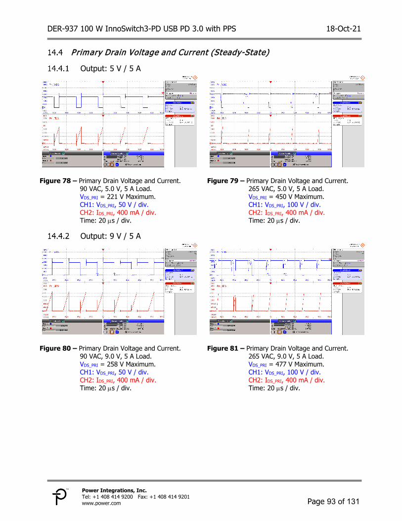
DER-937 100 W InnoSwitch3-PD USB PD 3.0 with PPS 18-Oct-21
Page 93 of 131
Power Integrations, Inc. Tel: +1 408 414 9200 Fax: +1 408 414 9201 www.power.com
Primary Drain Voltage and Current (Steady-State)
Output: 5 V / 5 A
Figure 78 – Primary Drain Voltage and Current.
90 VAC, 5.0 V, 5 A Load. VDS_PRI = 221 V Maximum. CH1: VDS_PRI, 50 V / div. CH2: IDS_PRI, 400 mA / div. Time: 20 µs / div.
Figure 79 – Primary Drain Voltage and Current. 265 VAC, 5.0 V, 5 A Load. VDS_PRI = 450 V Maximum. CH1: VDS_PRI, 100 V / div. CH2: IDS_PRI, 400 mA / div. Time: 20 µs / div.
Output: 9 V / 5 A
Figure 80 – Primary Drain Voltage and Current.
90 VAC, 9.0 V, 5 A Load. VDS_PRI = 258 V Maximum. CH1: VDS_PRI, 50 V / div. CH2: IDS_PRI, 400 mA / div. Time: 20 µs / div.
Figure 81 – Primary Drain Voltage and Current. 265 VAC, 9.0 V, 5 A Load. VDS_PRI = 477 V Maximum. CH1: VDS_PRI, 100 V / div. CH2: IDS_PRI, 400 mA / div. Time: 20 µs / div.
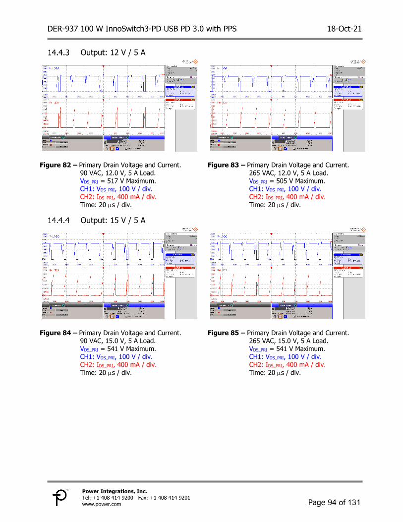
DER-937 100 W InnoSwitch3-PD USB PD 3.0 with PPS 18-Oct-21
Page 94 of 131
Power Integrations, Inc. Tel: +1 408 414 9200 Fax: +1 408 414 9201 www.power.com
Output: 12 V / 5 A
Figure 82 – Primary Drain Voltage and Current.
90 VAC, 12.0 V, 5 A Load. VDS_PRI = 517 V Maximum. CH1: VDS_PRI, 100 V / div. CH2: IDS_PRI, 400 mA / div. Time: 20 µs / div.
Figure 83 – Primary Drain Voltage and Current. 265 VAC, 12.0 V, 5 A Load. VDS_PRI = 505 V Maximum. CH1: VDS_PRI, 100 V / div. CH2: IDS_PRI, 400 mA / div. Time: 20 µs / div.
Output: 15 V / 5 A
Figure 84 – Primary Drain Voltage and Current.
90 VAC, 15.0 V, 5 A Load. VDS_PRI = 541 V Maximum. CH1: VDS_PRI, 100 V / div. CH2: IDS_PRI, 400 mA / div. Time: 20 µs / div.
Figure 85 – Primary Drain Voltage and Current. 265 VAC, 15.0 V, 5 A Load. VDS_PRI = 541 V Maximum. CH1: VDS_PRI, 100 V / div. CH2: IDS_PRI, 400 mA / div. Time: 20 µs / div.

DER-937 100 W InnoSwitch3-PD USB PD 3.0 with PPS 18-Oct-21
Page 95 of 131
Power Integrations, Inc. Tel: +1 408 414 9200 Fax: +1 408 414 9201 www.power.com
Output: 20 V / 5 A
Figure 86 – Primary Drain Voltage and Current.
90 VAC, 20.0 V, 5 A Load. VDS_PRI = 580 V Maximum. CH1: VDS_PRI, 100 V / div. CH2: IDS_PRI, 400 mA / div. Time: 20 µs / div.
Figure 87 – Primary Drain Voltage and Current. 265 VAC, 20.0 V, 5 A Load. VDS_PRI = 580 V Maximum. CH1: VDS_PRI, 100 V / div. CH2: IDS_PRI, 400 mA / div. Time: 20 µs / div.
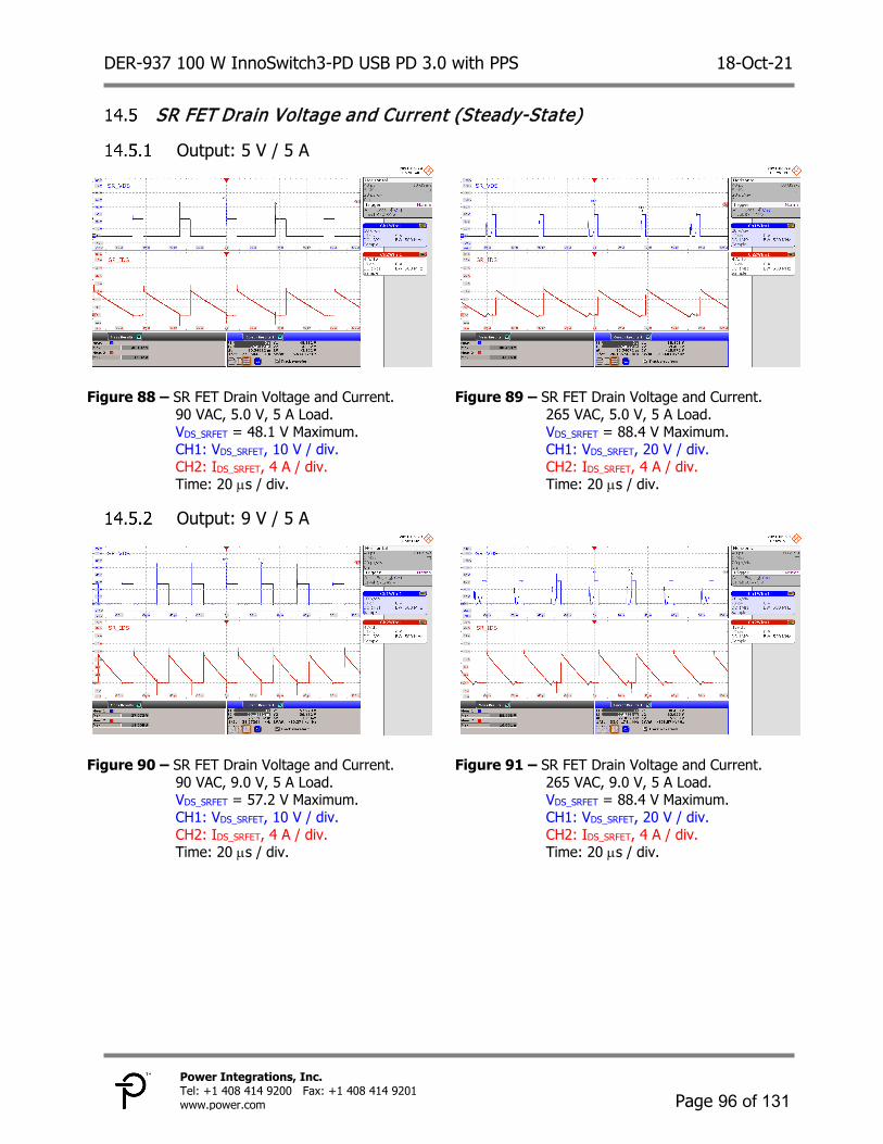
DER-937 100 W InnoSwitch3-PD USB PD 3.0 with PPS 18-Oct-21
Page 96 of 131
Power Integrations, Inc. Tel: +1 408 414 9200 Fax: +1 408 414 9201 www.power.com
SR FET Drain Voltage and Current (Steady-State)
Output: 5 V / 5 A
Figure 88 – SR FET Drain Voltage and Current.
90 VAC, 5.0 V, 5 A Load. VDS_SRFET = 48.1 V Maximum. CH1: VDS_SRFET, 10 V / div. CH2: IDS_SRFET, 4 A / div. Time: 20 µs / div.
Figure 89 – SR FET Drain Voltage and Current. 265 VAC, 5.0 V, 5 A Load. VDS_SRFET = 88.4 V Maximum. CH1: VDS_SRFET, 20 V / div. CH2: IDS_SRFET, 4 A / div. Time: 20 µs / div.
Output: 9 V / 5 A
Figure 90 – SR FET Drain Voltage and Current.
90 VAC, 9.0 V, 5 A Load. VDS_SRFET = 57.2 V Maximum. CH1: VDS_SRFET, 10 V / div. CH2: IDS_SRFET, 4 A / div. Time: 20 µs / div.
Figure 91 – SR FET Drain Voltage and Current. 265 VAC, 9.0 V, 5 A Load. VDS_SRFET = 88.4 V Maximum. CH1: VDS_SRFET, 20 V / div. CH2: IDS_SRFET, 4 A / div. Time: 20 µs / div.

DER-937 100 W InnoSwitch3-PD USB PD 3.0 with PPS 18-Oct-21
Page 97 of 131
Power Integrations, Inc. Tel: +1 408 414 9200 Fax: +1 408 414 9201 www.power.com
Output: 12 V / 5 A
Figure 92 – SR FET Drain Voltage and Current.
90 VAC, 12.0 V, 5 A Load. VDS_SRFET = 90.8 V Maximum. CH1: VDS_SRFET, 20 V / div. CH2: IDS_SRFET, 4 A / div. Time: 20 µs / div.
Figure 93 – SR FET Drain Voltage and Current. 265 VAC, 12.0 V, 5 A Load. VDS_SRFET = 89.2 V Maximum. CH1: VDS_SRFET, 20 V / div. CH2: IDS_SRFET, 4 A / div. Time: 20 µs / div.
Output: 15 V / 5 A
Figure 94 – SR FET Drain Voltage and Current.
90 VAC, 15.0 V, 5 A Load. VDS_SRFET = 91.6 V Maximum. CH1: VDS_SRFET, 20 V / div. CH2: IDS_SRFET, 4 A / div. Time: 20 µs / div.
Figure 95 – SR FET Drain Voltage and Current. 265 VAC, 15 V, 5 A Load. VDS_SRFET = 91.6 V Maximum. CH1: VDS_SRFET, 20 V / div. CH2: IDS_SRFET, 4 A / div. Time: 20 µs / div.

DER-937 100 W InnoSwitch3-PD USB PD 3.0 with PPS 18-Oct-21
Page 98 of 131
Power Integrations, Inc. Tel: +1 408 414 9200 Fax: +1 408 414 9201 www.power.com
Output: 20 V / 5 A
Figure 96 – SR FET Drain Voltage and Current.
90 VAC, 20.0 V, 5 A Load. VDS_SRFET = 94.7 V Maximum. CH1: VDS_SRFET, 20 V / div. CH2: IDS_SRFET, 4 A / div. Time: 20 µs / div.
Figure 97 – SR FET Drain Voltage and Current. 265 VAC, 20.0 V, 5 A Load. VDS_SRFET = 94.7 V Maximum. CH1: VDS_SRFET, 20 V / div. CH2: IDS_SRFET, 4 A / div. Time: 20 µs / div.

DER-937 100 W InnoSwitch3-PD USB PD 3.0 with PPS 18-Oct-21
Page 99 of 131
Power Integrations, Inc. Tel: +1 408 414 9200 Fax: +1 408 414 9201 www.power.com
Primary and SR FET Drain Voltage and Current (during Output Voltage Transition)
Primary Drain Voltage and Current, 3.3 V to 21 V PPS Transition Primary Drain Voltage, Drain Current, and output voltage on the board were captured. The USB PD Sink Request was changed from 3.3 V to 21 V / 5 A PPS (PDO6, 100 W Power-Limited) while the load current is at 4.5 A (~95% of current limit).
Figure 98 – Primary Drain Voltage and Current.
90 VAC, 3.3 V to 21 V VOUT Transition, 4.5 A Load. VDS_PRI = 608 V Maximum. CH1: VDS_PRI, 200 V / div. CH2: IDS_PRI, 1 A / div. CH4: VOUT, 4 V / div. Time: 20 ms / div. (50 µs / div. Zoom).
Figure 99 – Primary Drain Voltage and Current. 265 VAC, 3.3 V to 21 V VOUT Transition, 4.5 A Load. VDS_PRI = 592 V Maximum. CH1: VDS_PRI, 200 V / div. CH2: IDS_PRI, 1 A / div. CH4: VOUT, 4 V / div. Time: 20 ms / div. (50 µs / div. Zoom).
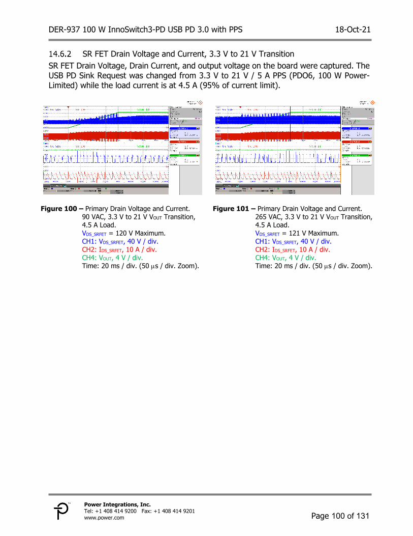
DER-937 100 W InnoSwitch3-PD USB PD 3.0 with PPS 18-Oct-21
Page 100 of 131
Power Integrations, Inc. Tel: +1 408 414 9200 Fax: +1 408 414 9201 www.power.com
SR FET Drain Voltage and Current, 3.3 V to 21 V Transition SR FET Drain Voltage, Drain Current, and output voltage on the board were captured. The USB PD Sink Request was changed from 3.3 V to 21 V / 5 A PPS (PDO6, 100 W Power-Limited) while the load current is at 4.5 A (95% of current limit).
Figure 100 – Primary Drain Voltage and Current.
90 VAC, 3.3 V to 21 V VOUT Transition, 4.5 A Load. VDS_SRFET = 120 V Maximum. CH1: VDS_SRFET, 40 V / div. CH2: IDS_SRFET, 10 A / div. CH4: VOUT, 4 V / div. Time: 20 ms / div. (50 µs / div. Zoom).
Figure 101 – Primary Drain Voltage and Current. 265 VAC, 3.3 V to 21 V VOUT Transition, 4.5 A Load. VDS_SRFET = 121 V Maximum. CH1: VDS_SRFET, 40 V / div. CH2: IDS_SRFET, 10 A / div. CH4: VOUT, 4 V / div. Time: 20 ms / div. (50 µs / div. Zoom).

DER-937 100 W InnoSwitch3-PD USB PD 3.0 with PPS 18-Oct-21
Page 101 of 131
Power Integrations, Inc. Tel: +1 408 414 9200 Fax: +1 408 414 9201 www.power.com
Load Transient Response Output voltage waveform on the board was captured with dynamic load transient from 10% to 100%. Duration for load states (high = 20 ms; low = 20 ms) was chosen to clearly show steady-state for each load condition. Load slew rate (150 mA / µs) is based on USB PD 3.0 specification. USB PD 3.0 specification allows a voltage overshoot/undershoot of ±0.5 V (vSrcValid) on top of ±5% tolerance from the operating voltage (vSrcNew) within the first 5 ms of applying a load transient (tSrcTransient). Beyond 5 ms, the voltage limits are tightened to ±5% within the operating voltage.
Output: 5 V / 5 A
Figure 102 – Transient Response.
90 VAC, 5.0 V, 0.5 to 5 A Load. VOUT = 5.15 V Max., 4.74 V Min. CH1: VOUT, 200 mV / div. CH2: IOUT, 2 A / div. Time: 20 ms / div. (200 µs / div. Zoom).
Figure 103 – Transient Response. 265 VAC, 5.0 V, 0.5 to 5 A Load. VOUT = 5.12 V Max., 4.74 V Min. CH1: VOUT, 200 mV / div. CH2: IOUT, 2 A / div. Time: 20 ms / div. (200 µs / div. Zoom).

DER-937 100 W InnoSwitch3-PD USB PD 3.0 with PPS 18-Oct-21
Page 102 of 131
Power Integrations, Inc. Tel: +1 408 414 9200 Fax: +1 408 414 9201 www.power.com
Output: 9 V / 5 A
Figure 104 – Transient Response.
90 VAC, 9.0 V, 0.5 to 5 A Load. VOUT = 9.21 V Max., 8.67 V Min. CH1: VOUT, 200 mV / div. CH2: IOUT, 2 A / div. Time: 20 ms / div. (200 µs / div. Zoom).
Figure 105 – Transient Response. 265 VAC, 9.0 V, 0.5 to 5 A Load. VOUT = 9.20 V Max., 8.73 V Min. CH1: VOUT, 200 mV / div. CH2: IOUT, 2 A / div. Time: 20 ms / div. (200 µs / div. Zoom).
Output: 12 V / 5 A
Figure 106 – Transient Response.
90 VAC, 12.0 V, 0.5 to 5 A Load. VOUT = 12.24 V Max., 11.45 V Min. CH1: VOUT, 2 V / div. CH2: IOUT, 2 A / div. Time: 20 ms / div. (200 µs / div. Zoom).
Figure 107 – Transient Response. 265 VAC, 12.0 V, 0.5 to 5 A Load. VOUT = 12.24 V Max., 11.61 V Min. CH1: VOUT, 2 V / div. CH2: IOUT, 2 A / div. Time: 20 ms / div. (200 µs / div. Zoom).
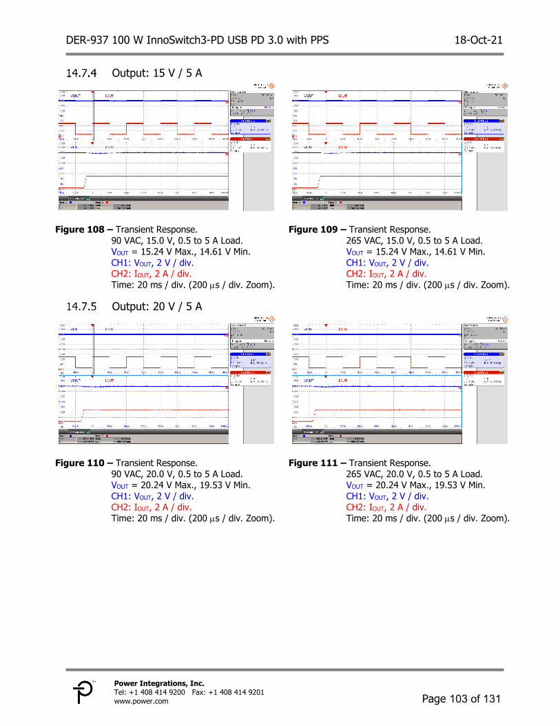
DER-937 100 W InnoSwitch3-PD USB PD 3.0 with PPS 18-Oct-21
Page 103 of 131
Power Integrations, Inc. Tel: +1 408 414 9200 Fax: +1 408 414 9201 www.power.com
Output: 15 V / 5 A
Figure 108 – Transient Response.
90 VAC, 15.0 V, 0.5 to 5 A Load. VOUT = 15.24 V Max., 14.61 V Min. CH1: VOUT, 2 V / div. CH2: IOUT, 2 A / div. Time: 20 ms / div. (200 µs / div. Zoom).
Figure 109 – Transient Response. 265 VAC, 15.0 V, 0.5 to 5 A Load. VOUT = 15.24 V Max., 14.61 V Min. CH1: VOUT, 2 V / div. CH2: IOUT, 2 A / div. Time: 20 ms / div. (200 µs / div. Zoom).
Output: 20 V / 5 A
Figure 110 – Transient Response.
90 VAC, 20.0 V, 0.5 to 5 A Load. VOUT = 20.24 V Max., 19.53 V Min. CH1: VOUT, 2 V / div. CH2: IOUT, 2 A / div. Time: 20 ms / div. (200 µs / div. Zoom).
Figure 111 – Transient Response. 265 VAC, 20.0 V, 0.5 to 5 A Load. VOUT = 20.24 V Max., 19.53 V Min. CH1: VOUT, 2 V / div. CH2: IOUT, 2 A / div. Time: 20 ms / div. (200 µs / div. Zoom).
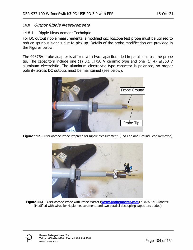
DER-937 100 W InnoSwitch3-PD USB PD 3.0 with PPS 18-Oct-21
Page 104 of 131
Power Integrations, Inc. Tel: +1 408 414 9200 Fax: +1 408 414 9201 www.power.com
Output Ripple Measurements
Ripple Measurement Technique For DC output ripple measurements, a modified oscilloscope test probe must be utilized to reduce spurious signals due to pick-up. Details of the probe modification are provided in the Figures below. The 4987BA probe adapter is affixed with two capacitors tied in parallel across the probe tip. The capacitors include one (1) 0.1 µF/50 V ceramic type and one (1) 47 µF/50 V aluminum electrolytic. The aluminum electrolytic type capacitor is polarized, so proper polarity across DC outputs must be maintained (see below).
Figure 112 – Oscilloscope Probe Prepared for Ripple Measurement. (End Cap and Ground Lead Removed)
Figure 113 – Oscilloscope Probe with Probe Master (www.probemaster.com) 4987A BNC Adapter.
(Modified with wires for ripple measurement, and two parallel decoupling capacitors added)
Probe Ground
Probe Tip
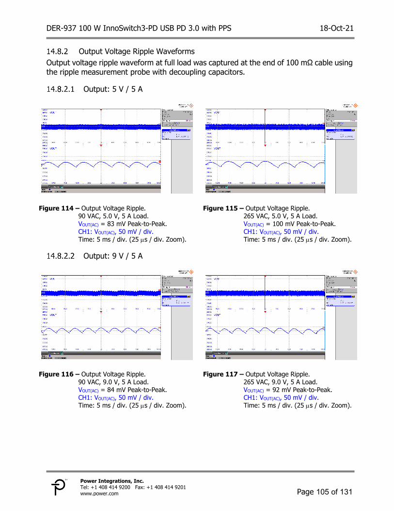
DER-937 100 W InnoSwitch3-PD USB PD 3.0 with PPS 18-Oct-21
Page 105 of 131
Power Integrations, Inc. Tel: +1 408 414 9200 Fax: +1 408 414 9201 www.power.com
Output Voltage Ripple Waveforms Output voltage ripple waveform at full load was captured at the end of 100 mΩ cable using the ripple measurement probe with decoupling capacitors.
Output: 5 V / 5 A
Figure 114 – Output Voltage Ripple.
90 VAC, 5.0 V, 5 A Load. VOUT(AC) = 83 mV Peak-to-Peak. CH1: VOUT(AC), 50 mV / div. Time: 5 ms / div. (25 µs / div. Zoom).
Figure 115 – Output Voltage Ripple. 265 VAC, 5.0 V, 5 A Load. VOUT(AC) = 100 mV Peak-to-Peak. CH1: VOUT(AC), 50 mV / div. Time: 5 ms / div. (25 µs / div. Zoom).
Output: 9 V / 5 A
Figure 116 – Output Voltage Ripple.
90 VAC, 9.0 V, 5 A Load. VOUT(AC) = 84 mV Peak-to-Peak. CH1: VOUT(AC), 50 mV / div. Time: 5 ms / div. (25 µs / div. Zoom).
Figure 117 – Output Voltage Ripple. 265 VAC, 9.0 V, 5 A Load. VOUT(AC) = 92 mV Peak-to-Peak. CH1: VOUT(AC), 50 mV / div. Time: 5 ms / div. (25 µs / div. Zoom).
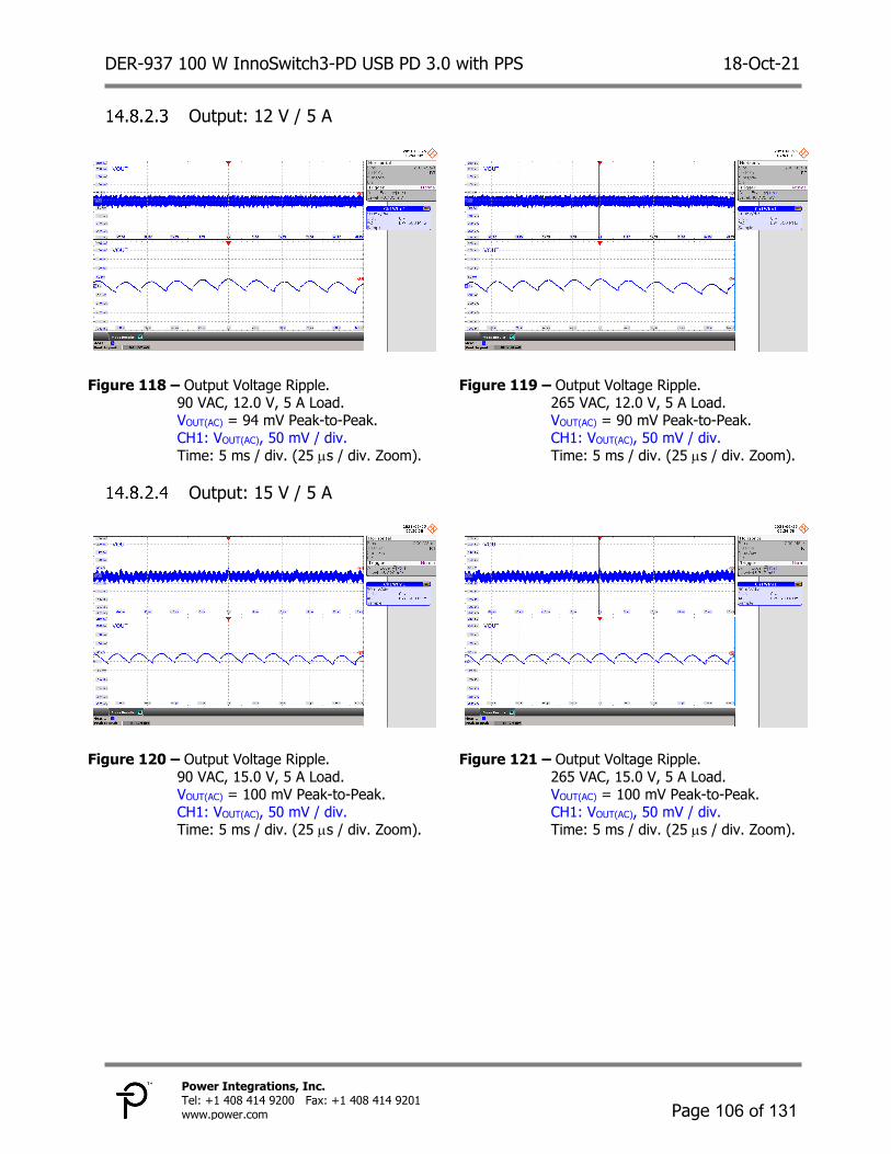
DER-937 100 W InnoSwitch3-PD USB PD 3.0 with PPS 18-Oct-21
Page 106 of 131
Power Integrations, Inc. Tel: +1 408 414 9200 Fax: +1 408 414 9201 www.power.com
Output: 12 V / 5 A
Figure 118 – Output Voltage Ripple.
90 VAC, 12.0 V, 5 A Load. VOUT(AC) = 94 mV Peak-to-Peak. CH1: VOUT(AC), 50 mV / div. Time: 5 ms / div. (25 µs / div. Zoom).
Figure 119 – Output Voltage Ripple. 265 VAC, 12.0 V, 5 A Load. VOUT(AC) = 90 mV Peak-to-Peak. CH1: VOUT(AC), 50 mV / div. Time: 5 ms / div. (25 µs / div. Zoom).
Output: 15 V / 5 A
Figure 120 – Output Voltage Ripple.
90 VAC, 15.0 V, 5 A Load. VOUT(AC) = 100 mV Peak-to-Peak. CH1: VOUT(AC), 50 mV / div. Time: 5 ms / div. (25 µs / div. Zoom).
Figure 121 – Output Voltage Ripple. 265 VAC, 15.0 V, 5 A Load. VOUT(AC) = 100 mV Peak-to-Peak. CH1: VOUT(AC), 50 mV / div. Time: 5 ms / div. (25 µs / div. Zoom).
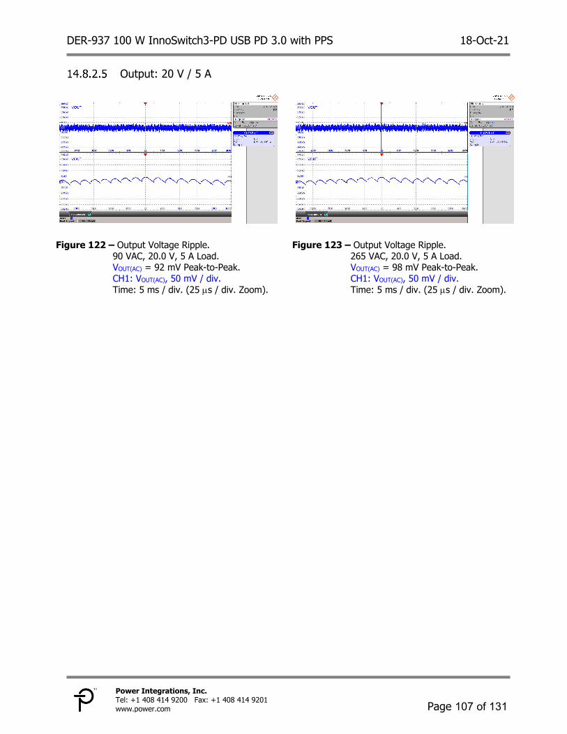
DER-937 100 W InnoSwitch3-PD USB PD 3.0 with PPS 18-Oct-21
Page 107 of 131
Power Integrations, Inc. Tel: +1 408 414 9200 Fax: +1 408 414 9201 www.power.com
Output: 20 V / 5 A
Figure 122 – Output Voltage Ripple.
90 VAC, 20.0 V, 5 A Load. VOUT(AC) = 92 mV Peak-to-Peak. CH1: VOUT(AC), 50 mV / div. Time: 5 ms / div. (25 µs / div. Zoom).
Figure 123 – Output Voltage Ripple. 265 VAC, 20.0 V, 5 A Load. VOUT(AC) = 98 mV Peak-to-Peak. CH1: VOUT(AC), 50 mV / div. Time: 5 ms / div. (25 µs / div. Zoom).
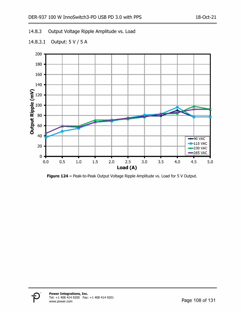
DER-937 100 W InnoSwitch3-PD USB PD 3.0 with PPS 18-Oct-21
Page 108 of 131
Power Integrations, Inc. Tel: +1 408 414 9200 Fax: +1 408 414 9201 www.power.com
Output Voltage Ripple Amplitude vs. Load
Output: 5 V / 5 A
Figure 124 – Peak-to-Peak Output Voltage Ripple Amplitude vs. Load for 5 V Output.

DER-937 100 W InnoSwitch3-PD USB PD 3.0 with PPS 18-Oct-21
Page 109 of 131
Power Integrations, Inc. Tel: +1 408 414 9200 Fax: +1 408 414 9201 www.power.com
Output: 9 V / 5 A
Figure 125 – Peak-to-Peak Output Voltage Ripple Amplitude vs. Load for 9 V Output.

DER-937 100 W InnoSwitch3-PD USB PD 3.0 with PPS 18-Oct-21
Page 110 of 131
Power Integrations, Inc. Tel: +1 408 414 9200 Fax: +1 408 414 9201 www.power.com
Output: 12 V / 5 A
Figure 126 – Peak-to-Peak Output Voltage Ripple Amplitude vs. Load for 12 V Output.
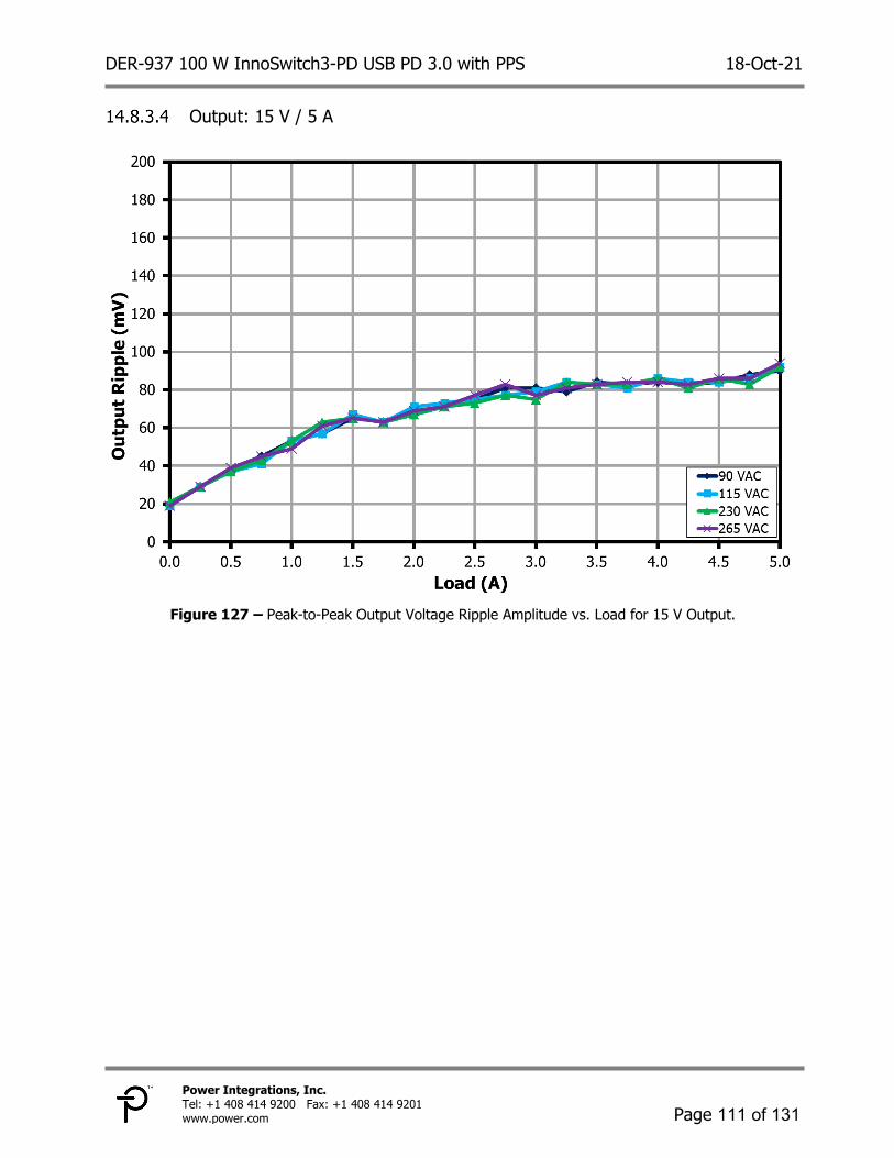
DER-937 100 W InnoSwitch3-PD USB PD 3.0 with PPS 18-Oct-21
Page 111 of 131
Power Integrations, Inc. Tel: +1 408 414 9200 Fax: +1 408 414 9201 www.power.com
Output: 15 V / 5 A
Figure 127 – Peak-to-Peak Output Voltage Ripple Amplitude vs. Load for 15 V Output.

DER-937 100 W InnoSwitch3-PD USB PD 3.0 with PPS 18-Oct-21
Page 112 of 131
Power Integrations, Inc. Tel: +1 408 414 9200 Fax: +1 408 414 9201 www.power.com
Output: 20 V / 5 A
Figure 128 – Peak-to-Peak Output Voltage Ripple Amplitude vs. Load for 20 V Output.

DER-937 100 W InnoSwitch3-PD USB PD 3.0 with PPS 18-Oct-21
Page 113 of 131
Power Integrations, Inc. Tel: +1 408 414 9200 Fax: +1 408 414 9201 www.power.com
CV/CC Profile One Programmable Power Supply (PPS) Augmented Power Data Object (APDO) is supported in this design:
• PDO6: 3.3 V – 21 V / 5 A PPS (100 W power-limited) CVCC profiles were taken with the output voltage measured on the board.
Output: 20 V / 5 A PPS Request, PDO6 (100 W Power-Limited)
Figure 129 – CV/CC Profile for 20 V / 5 A PPS Request.

DER-937 100 W InnoSwitch3-PD USB PD 3.0 with PPS 18-Oct-21
Page 114 of 131
Power Integrations, Inc. Tel: +1 408 414 9200 Fax: +1 408 414 9201 www.power.com
Output: 21 V / 5 A PPS Request, PDO6 (100 W Power-Limited)
Figure 130 – CV/CC Profile for 21 V / 5 A PPS Request.

DER-937 100 W InnoSwitch3-PD USB PD 3.0 with PPS 18-Oct-21
Page 115 of 131
Power Integrations, Inc. Tel: +1 408 414 9200 Fax: +1 408 414 9201 www.power.com
Voltage Step and Current Limit Test using QuadraMAX and Total Phase Analyzer
The power supply was evaluated and passed both QuadraMAX PPS Voltage Step Test (VST) and PPS Current Limit Test (CLT). The output voltage and current during VST and CLT as recorded by the Total Phase Analyzer are presented below.
Voltage Step Test (VST)
Figure 131 – Plot of SPT.6 VST from Total Phase Analyzer.

DER-937 100 W InnoSwitch3-PD USB PD 3.0 with PPS 18-Oct-21
Page 116 of 131
Power Integrations, Inc. Tel: +1 408 414 9200 Fax: +1 408 414 9201 www.power.com
Current Limit Test (CLT)
Figure 132 – Plot of SPT.7 CLT from Total Phase Analyzer.
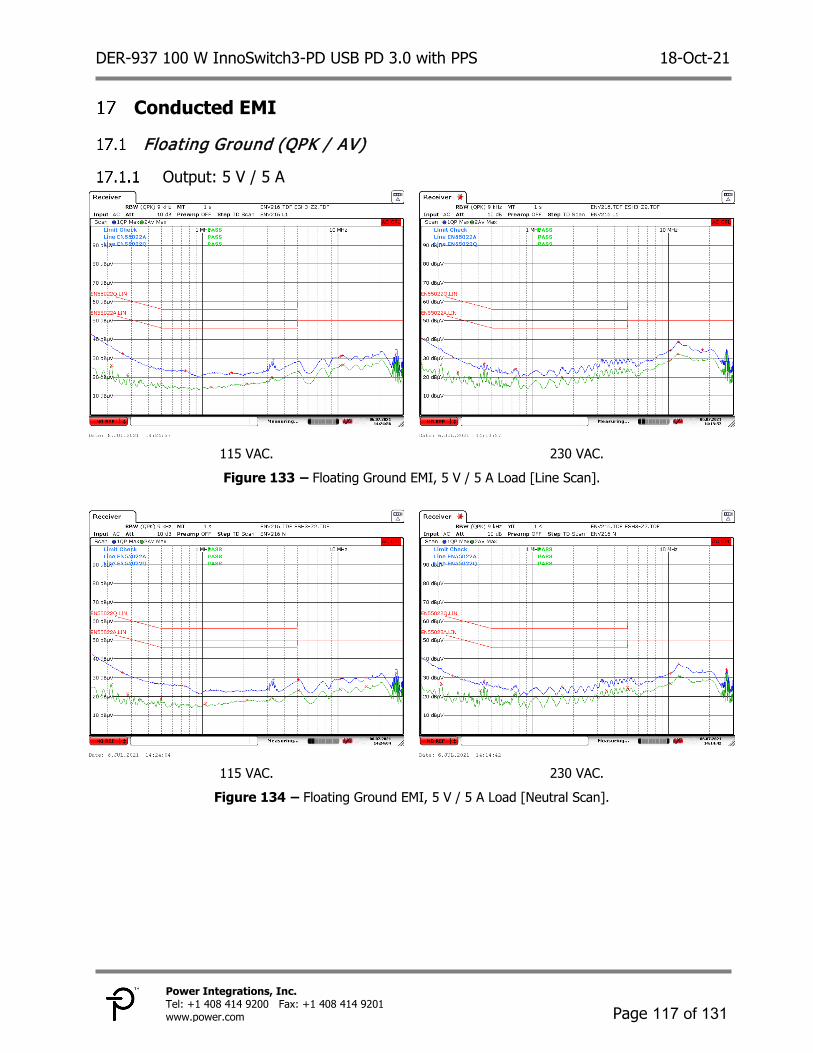
DER-937 100 W InnoSwitch3-PD USB PD 3.0 with PPS 18-Oct-21
Page 117 of 131
Power Integrations, Inc. Tel: +1 408 414 9200 Fax: +1 408 414 9201 www.power.com
Conducted EMI
Floating Ground (QPK / AV)
Output: 5 V / 5 A
115 VAC. 230 VAC. Figure 133 – Floating Ground EMI, 5 V / 5 A Load [Line Scan].
115 VAC. 230 VAC.
Figure 134 – Floating Ground EMI, 5 V / 5 A Load [Neutral Scan].

DER-937 100 W InnoSwitch3-PD USB PD 3.0 with PPS 18-Oct-21
Page 118 of 131
Power Integrations, Inc. Tel: +1 408 414 9200 Fax: +1 408 414 9201 www.power.com
Output: 9 V / 5 A
115 VAC. 230 VAC. Figure 135 – Floating Ground EMI, 9 V / 5 A Load [Line Scan].
115 VAC. 230 VAC.
Figure 136 – Floating Ground EMI, 9 V / 5 A Load [Neutral Scan].
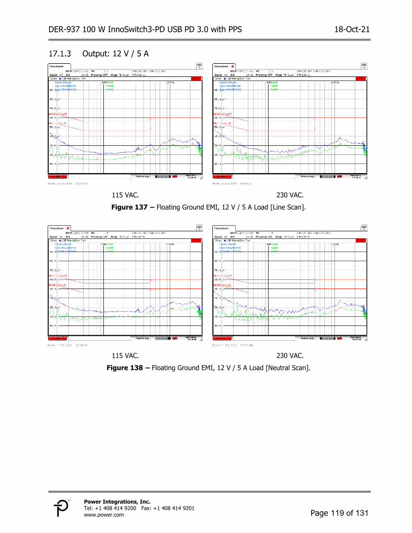
DER-937 100 W InnoSwitch3-PD USB PD 3.0 with PPS 18-Oct-21
Page 119 of 131
Power Integrations, Inc. Tel: +1 408 414 9200 Fax: +1 408 414 9201 www.power.com
Output: 12 V / 5 A
115 VAC. 230 VAC. Figure 137 – Floating Ground EMI, 12 V / 5 A Load [Line Scan].
115 VAC. 230 VAC.
Figure 138 – Floating Ground EMI, 12 V / 5 A Load [Neutral Scan].

DER-937 100 W InnoSwitch3-PD USB PD 3.0 with PPS 18-Oct-21
Page 120 of 131
Power Integrations, Inc. Tel: +1 408 414 9200 Fax: +1 408 414 9201 www.power.com
Output: 15 V / 5 A
115 VAC. 230 VAC. Figure 139 – Floating Ground EMI, 15 V / 5 A Load [Line Scan].
115 VAC. 230 VAC.
Figure 140 – Floating Ground EMI, 15 V / 5 A Load [Neutral Scan].

DER-937 100 W InnoSwitch3-PD USB PD 3.0 with PPS 18-Oct-21
Page 121 of 131
Power Integrations, Inc. Tel: +1 408 414 9200 Fax: +1 408 414 9201 www.power.com
Output: 20 V / 5 A
115 VAC. 230 VAC. Figure 141 – Floating Ground EMI, 20 V / 5 A Load [Line Scan].
115 VAC. 230 VAC.
Figure 142 – Floating Ground EMI, 20 V / 5 A Load [Neutral Scan].

DER-937 100 W InnoSwitch3-PD USB PD 3.0 with PPS 18-Oct-21
Page 122 of 131
Power Integrations, Inc. Tel: +1 408 414 9200 Fax: +1 408 414 9201 www.power.com
Combination Wave Surge The unit was subjected to ±1000 V differential mode and ±2000 V common mode combination wave surge at several line phase angles with 10 strikes for each condition. A test failure was defined as an output latch-off that needs operator intervention to recover, or a complete loss of function that is not recoverable.
Differential Mode Surge (L1 to L2), 230 VAC Input Surge Level (V)
Injection Location
Injection Phase
(°)
Test Result 5 V / 0 A
without PD Sink Test Result 20 V / 5 A
+1000 L1 to L2 0 Pass Pass -1000 L1 to L2 0 Pass Pass +1000 L1 to L2 90 Pass Pass -1000 L1 to L2 90 Pass Pass +1000 L1 to L2 270 Pass Pass -1000 L1 to L2 270 Pass Pass
Common Mode Surge (L1, L2 to PE), 230 VAC Input Surge Level (V)
Injection Location
Injection Phase
(°)
Test Result 5 V / 0 A
without PD Sink Test Result 20 V / 5 A
+2000 L1, L2 to PE 0 Pass Pass -2000 L1, L2 to PE 0 Pass Pass +2000 L1, L2 to PE 90 Pass Pass -2000 L1, L2 to PE 90 Pass Pass +2000 L1, L2 to PE 270 Pass Pass -2000 L1, L2 to PE 270 Pass Pass
Common Mode Surge (L1 to PE), 230 VAC Input Surge Level (V)
Injection Location
Injection Phase
(°)
Test Result 5 V / 0 A
without PD Sink Test Result 20 V / 5 A
+2000 L1 to PE 0 Pass Pass -2000 L1 to PE 0 Pass Pass +2000 L1 to PE 90 Pass Pass -2000 L1 to PE 90 Pass Pass +2000 L1 to PE 270 Pass Pass -2000 L1 to PE 270 Pass Pass
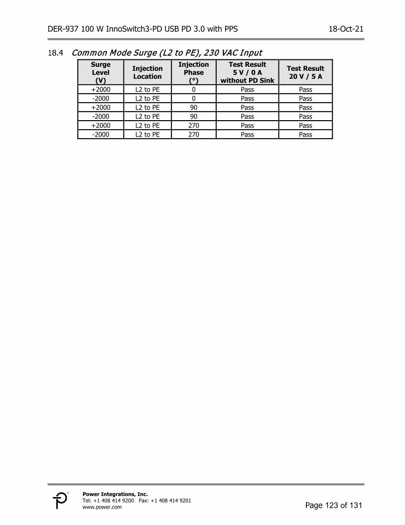
DER-937 100 W InnoSwitch3-PD USB PD 3.0 with PPS 18-Oct-21
Page 123 of 131
Power Integrations, Inc. Tel: +1 408 414 9200 Fax: +1 408 414 9201 www.power.com
Common Mode Surge (L2 to PE), 230 VAC Input Surge Level (V)
Injection Location
Injection Phase
(°)
Test Result 5 V / 0 A
without PD Sink Test Result 20 V / 5 A
+2000 L2 to PE 0 Pass Pass -2000 L2 to PE 0 Pass Pass +2000 L2 to PE 90 Pass Pass -2000 L2 to PE 90 Pass Pass +2000 L2 to PE 270 Pass Pass -2000 L2 to PE 270 Pass Pass

DER-937 100 W InnoSwitch3-PD USB PD 3.0 with PPS 18-Oct-21
Page 124 of 131
Power Integrations, Inc. Tel: +1 408 414 9200 Fax: +1 408 414 9201 www.power.com
Electrostatic Discharge The unit was tested with ±8.0 kV to ±16.5 kV air discharge and ±8.0 to ±8.8 kV contact discharge with 10 strikes for each condition at the following locations: • End of cable +VOUT and GND • End of cable USB PD Sink CC Lines • On-board +VOUT and GND A test failure was defined as an output latch-off that needs operator intervention to recover, or a complete loss of function that is not recoverable.
VOUT and GND ESD Performance Discharge points were added on the board and at the end of cable on the USB PD Sink (TinyPAT) to test VOUT and GND ESD performance. A 1-meter 5 A USB Type C cable with e-marker (Veckle) was used to support 100 W load.
Figure 143 – ESD Discharge Points.
On-board GND
On-board VOUT
End of cable VOUT
End of cable GND
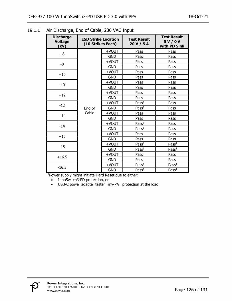
DER-937 100 W InnoSwitch3-PD USB PD 3.0 with PPS 18-Oct-21
Page 125 of 131
Power Integrations, Inc. Tel: +1 408 414 9200 Fax: +1 408 414 9201 www.power.com
Air Discharge, End of Cable, 230 VAC Input Discharge
Voltage (kV)
ESD Strike Location (10 Strikes Each)
Test Result 20 V / 5 A
Test Result 5 V / 0 A
with PD Sink
+8
End of Cable
+VOUT Pass Pass GND Pass Pass
-8 +VOUT Pass Pass GND Pass Pass
+10 +VOUT Pass Pass GND Pass Pass
-10 +VOUT Pass Pass GND Pass Pass
+12 +VOUT Pass Pass GND Pass Pass
-12 +VOUT Pass1 Pass GND Pass1 Pass
+14 +VOUT Pass Pass GND Pass Pass
-14 +VOUT Pass1 Pass GND Pass1 Pass
+15 +VOUT Pass Pass GND Pass Pass
-15 +VOUT Pass1 Pass1 GND Pass1 Pass1
+16.5 +VOUT Pass Pass GND Pass Pass
-16.5 +VOUT Pass1 Pass1 GND Pass1 Pass1
1Power supply might initiate Hard Reset due to either: • InnoSwitch3-PD protection, or • USB-C power adapter tester Tiny-PAT protection at the load
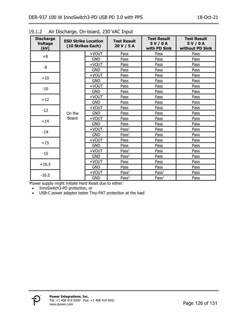
DER-937 100 W InnoSwitch3-PD USB PD 3.0 with PPS 18-Oct-21
Page 126 of 131
Power Integrations, Inc. Tel: +1 408 414 9200 Fax: +1 408 414 9201 www.power.com
Air Discharge, On-board, 230 VAC Input Discharge
Voltage (kV)
ESD Strike Location (10 Strikes Each)
Test Result 20 V / 5 A
Test Result 5 V / 0 A
with PD Sink
Test Result 5 V / 0 A
without PD Sink
+8
On the Board
+VOUT Pass Pass Pass GND Pass Pass Pass
-8 +VOUT Pass Pass Pass GND Pass Pass Pass
+10 +VOUT Pass Pass Pass GND Pass Pass Pass
-10 +VOUT Pass Pass Pass GND Pass Pass Pass
+12 +VOUT Pass Pass Pass GND Pass Pass Pass
-12 +VOUT Pass Pass Pass GND Pass Pass Pass
+14 +VOUT Pass Pass Pass GND Pass Pass Pass
-14 +VOUT Pass1 Pass Pass GND Pass1 Pass Pass
+15 +VOUT Pass Pass Pass GND Pass Pass Pass
-15 +VOUT Pass1 Pass Pass GND Pass1 Pass Pass
+16.5 +VOUT Pass Pass Pass GND Pass Pass Pass
-16.5 +VOUT Pass1 Pass1 Pass GND Pass1 Pass1 Pass
1Power supply might initiate Hard Reset due to either: • InnoSwitch3-PD protection, or • USB-C power adapter tester Tiny-PAT protection at the load

DER-937 100 W InnoSwitch3-PD USB PD 3.0 with PPS 18-Oct-21
Page 127 of 131
Power Integrations, Inc. Tel: +1 408 414 9200 Fax: +1 408 414 9201 www.power.com
Contact Discharge, End of Cable, 230 VAC Input Discharge
Voltage (kV)
ESD Strike Location (10 Strikes Each)
Test Result 20 V / 5 A
Test Result 5 V / 0 A
with PD Sink
+8.0
End of Cable
+VOUT Pass1 Pass GND Pass1 Pass
-8.0 +VOUT Pass1 Pass GND Pass1 Pass
+8.8 +VOUT Pass1 Pass1 GND Pass1 Pass1
-8.8 +VOUT Pass1 Pass1 GND Pass1 Pass1
1Power supply might initiate Hard Reset due to either: • InnoSwitch3-PD protection, or • USB-C power adapter tester Tiny-PAT protection at the load
Contact Discharge, On the Board, 230 VAC Input Discharge
Voltage (kV)
ESD Strike Location (10 Strikes Each)
Test Result 20 V / 5 A
Test Result 5 V / 0 A
with PD Sink
Test Result 5 V / 0 A
without PD Sink
+8.0
On the Board
+VOUT Pass Pass Pass GND Pass Pass Pass
-8.0 +VOUT Pass Pass Pass GND Pass Pass Pass
+8.8 +VOUT Pass Pass Pass GND Pass Pass Pass
-8.8 +VOUT Pass Pass Pass GND Pass Pass Pass
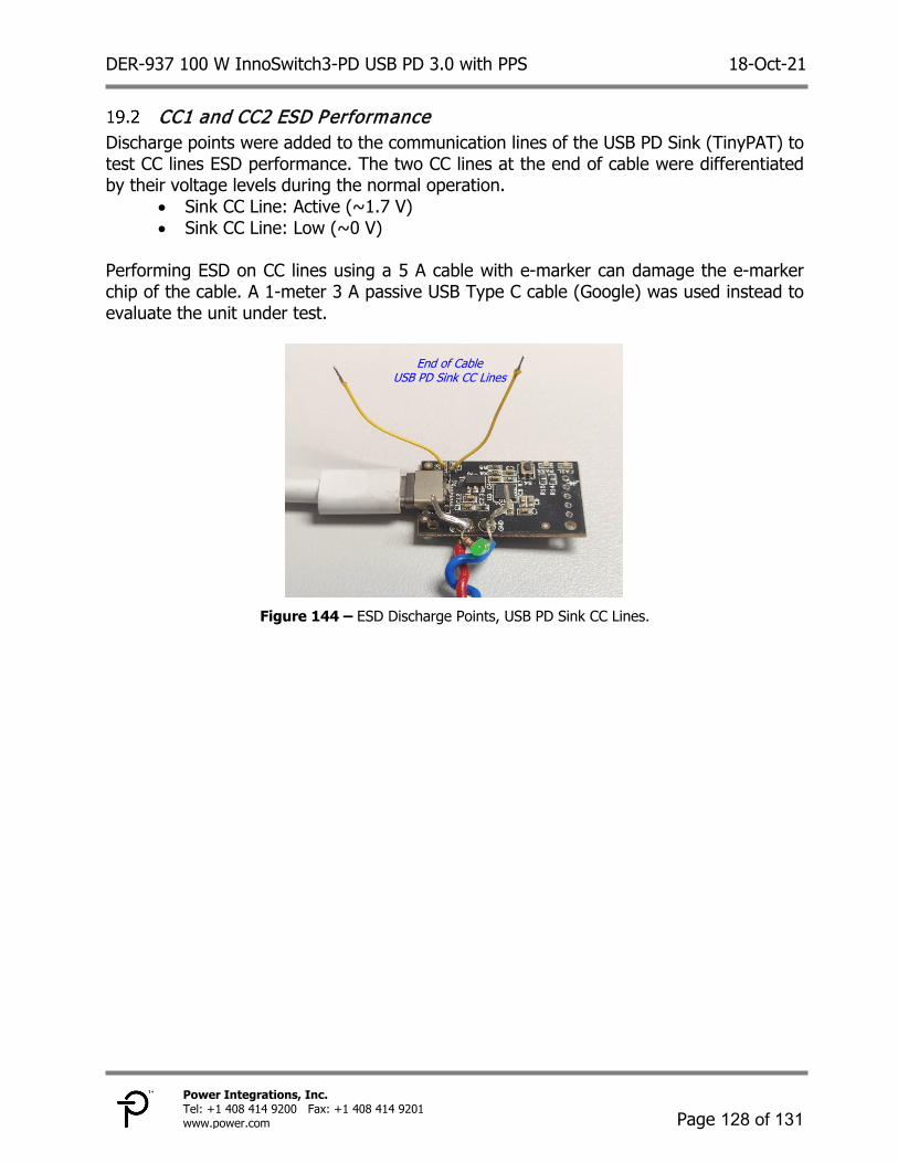
DER-937 100 W InnoSwitch3-PD USB PD 3.0 with PPS 18-Oct-21
Page 128 of 131
Power Integrations, Inc. Tel: +1 408 414 9200 Fax: +1 408 414 9201 www.power.com
CC1 and CC2 ESD Performance Discharge points were added to the communication lines of the USB PD Sink (TinyPAT) to test CC lines ESD performance. The two CC lines at the end of cable were differentiated by their voltage levels during the normal operation.
• Sink CC Line: Active (~1.7 V) • Sink CC Line: Low (~0 V)
Performing ESD on CC lines using a 5 A cable with e-marker can damage the e-marker chip of the cable. A 1-meter 3 A passive USB Type C cable (Google) was used instead to evaluate the unit under test.
Figure 144 – ESD Discharge Points, USB PD Sink CC Lines.
End of Cable USB PD Sink CC Lines

DER-937 100 W InnoSwitch3-PD USB PD 3.0 with PPS 18-Oct-21
Page 129 of 131
Power Integrations, Inc. Tel: +1 408 414 9200 Fax: +1 408 414 9201 www.power.com
Air Discharge, End of cable, 230 VAC Input Discharge
Voltage (kV)
ESD Strike Location (10 Strikes Each)
Test Result 20 V / 3 A
Test Result 5 V / 0 A
with PD Sink
+15
End of Cable
CC Line: Active Pass1 Pass1 CC Line: Low Pass1 Pass1
-15 CC Line: Active Pass1 Pass1 CC Line: Low Pass1 Pass1
+16.5 CC Line: Active Pass1 Pass1 CC Line: Low Pass1 Pass1
-16.5 CC Line: Active Pass1 Pass1 CC Line: Low Pass1 Pass1
1Power supply might initiate Hard Reset due to either: • InnoSwitch3-PD protection, or • USB-C power adapter tester Tiny-PAT protection at the load
Contact Discharge, End of Cable, 230 VAC Input Discharge
Voltage (kV)
ESD Strike Location (10 Strikes Each)
Test Result 20 V / 3 A
Test Result 5 V / 0 A
with PD Sink
+8.0
End of Cable
CC Line: Active Pass1 Pass1 CC Line: Low Pass1 Pass1
-8.0 CC Line: Active Pass1 Pass1 CC Line: Low Pass1 Pass1
+8.8 CC Line: Active Pass1 Pass1 CC Line: Low Pass1 Pass1
-8.8 CC Line: Active Pass1 Pass1 CC Line: Low Pass1 Pass1
1Power supply might initiate Hard Reset due to either: • InnoSwitch3-PD protection, or • USB-C power adapter tester Tiny-PAT protection at the load

DER-937 100 W InnoSwitch3-PD USB PD 3.0 with PPS 18-Oct-21
Page 130 of 131
Power Integrations, Inc. Tel: +1 408 414 9200 Fax: +1 408 414 9201 www.power.com
Revision History Date Author Revision Description & Changes Reviewed
18-Oct-21 DB 1.0 Initial Release. Apps & Mktg

DER-937 100 W InnoSwitch3-PD USB PD 3.0 with PPS 18-Oct-21
Page 131 of 131
Power Integrations, Inc. Tel: +1 408 414 9200 Fax: +1 408 414 9201 www.power.com
For the latest updates, visit our website: www.power.com Reference Designs are technical proposals concerning how to use Power Integrations’ gate drivers in particular applications and/or with certain power modules. These proposals are “as is” and are not subject to any qualification process. The suitability, implementation and qualification are the sole responsibility of the end user. The statements, technical information and recommendations contained herein are believed to be accurate as of the date hereof. All parameters, numbers, values and other technical data included in the technical information were calculated and determined to our best knowledge in accordance with the relevant technical norms (if any). They may base on assumptions or operational conditions that do not necessarily apply in general. We exclude any representation or warranty, express or implied, in relation to the accuracy or completeness of the statements, technical information and recommendations contained herein. No responsibility is accepted for the accuracy or sufficiency of any of the statements, technical information, recommendations or opinions communicated and any liability for any direct, indirect or consequential loss or damage suffered by any person arising therefrom is expressly disclaimed. Power Integrations reserves the right to make changes to its products at any time to improve reliability or manufacturability. Power Integrations does not assume any liability arising from the use of any device or circuit described herein. POWER INTEGRATIONS MAKES NO WARRANTY HEREIN AND SPECIFICALLY DISCLAIMS ALL WARRANTIES INCLUDING, WITHOUT LIMITATION, THE IMPLIED WARRANTIES OF MERCHANTABILITY, FITNESS FOR A PARTICULAR PURPOSE, AND NON-INFRINGEMENT OF THIRD PARTY RIGHTS. Patent Information The products and applications illustrated herein (including transformer construction and circuits’ external to the products) may be covered by one or more U.S. and foreign patents, or potentially by pending U.S. and foreign patent applications assigned to Power Integrations. A complete list of Power Integrations’ patents may be found at www.power.com. Power Integrations grants its customers a license under certain patent rights as set forth at http://www.power.com/ip.htm. Power Integrations, the Power Integrations logo, CAPZero, ChiPhy, CHY, DPA-Switch, EcoSmart, E-Shield, eSIP, eSOP, HiperPLC, HiperPFS, HiperTFS, InnoSwitch, Innovation in Power Conversion, InSOP, LinkSwitch, LinkZero, LYTSwitch, SENZero, TinySwitch, TOPSwitch, PI, PI Expert, SCALE, SCALE-1, SCALE-2, SCALE-3 and SCALE-iDriver, are trademarks of Power Integrations, Inc. Other trademarks are property of their respective companies. ©2019, Power Integrations, Inc. Power Integrations Worldwide Sales Support Locations
WORLD HEADQUARTERS 5245 Hellyer Avenue San Jose, CA 95138, USA. Main: +1-408-414-9200 Customer Service: Worldwide: +1-65-635-64480 Americas: +1-408-414-9621 e-mail: [email protected] CHINA (SHANGHAI) Rm 2410, Charity Plaza, No. 88, North Caoxi Road, Shanghai, PRC 200030 Phone: +86-21-6354-6323 e-mail: [email protected] CHINA (SHENZHEN) 17/F, Hivac Building, No. 2, Keji Nan 8th Road, Nanshan District, Shenzhen, China, 518057 Phone: +86-755-8672-8689 e-mail: [email protected]
GERMANY (AC-DC/LED Sales) Einsteinring 24 85609 Dornach/Aschheim Germany Tel: +49-89-5527-39100 e-mail: [email protected] GERMANY (Gate Driver Sales) HellwegForum 1 59469 Ense Germany Tel: +49-2938-64-39990 e-mail: igbt-driver.sales@ power.com INDIA #1, 14th Main Road Vasanthanagar Bangalore-560052 India Phone: +91-80-4113-8020 e-mail: [email protected]
ITALY Via Milanese 20, 3rd. Fl. 20099 Sesto San Giovanni (MI) Italy Phone: +39-024-550-8701 e-mail: [email protected] JAPAN Yusen Shin-Yokohama 1-chome Bldg. 1-7-9, Shin-Yokohama, Kohoku-ku Yokohama-shi, Kanagawa 222-0033 Japan Phone: +81-45-471-1021 e-mail: [email protected] KOREA RM 602, 6FL Korea City Air Terminal B/D, 159-6 Samsung-Dong, Kangnam-Gu, Seoul, 135-728 Korea Phone: +82-2-2016-6610 e-mail: [email protected]
SINGAPORE 51 Newton Road, #19-01/05 Goldhill Plaza Singapore, 308900 Phone: +65-6358-2160 e-mail: [email protected]
TAIWAN 5F, No. 318, Nei Hu Rd., Sec. 1 Nei Hu District Taipei 11493, Taiwan R.O.C. Phone: +886-2-2659-4570 e-mail: [email protected] UK Building 5, Suite 21 The Westbrook Centre Milton Road Cambridge CB4 1YG Phone: +44 (0) 7823-557484 e-mail: [email protected]
Copyright © 2022 FDOKUMEN