
Design Example Report - 20 W USB PD 3.0 Power Supply with 3.3 V
76
Power Integrations 5245 Hellyer Avenue, San Jose, CA 95138 USA. Tel: +1 408 414 9200 Fax: +1 408 414 9201 www.power.com Design Example Report Title 20 W USB PD 3.0 Power Supply with 3.3 V – 11 V PPS Output Using InnoSwitch TM 3-Pro INN3365C-H302 and VIA Labs VP302 Controller Specification 90 VAC – 265 VAC Input; 5 V / 3 A; 9 V / 2.23 A; or 3.3 V – 11 V PPS Output Application Mobile Phone Charger Author Applications Engineering Department Document Number DER-820 Date November 5, 2019 Revision 4.0 Summary and Features • InnoSwitch3-Pro - digitally controllable CV/CC QR flyback switcher IC with integrated high- voltage MOSFET, synchronous rectification and FluxLink TM feedback I 2 C Interface enables low pin count USB PD controller (8 pin) Sophisticated telemetry and comprehensive protection features • USB PD 3.0 with PPS using highly optimized, low pin count USB PD controller VP302 • All the benefits of secondary-side control with the simplicity of primary-side regulation Insensitive to transformer variation • Meets DOE6 and CoC v5 2016 efficiency requirement • Micro stepping of voltages (20 mV) and CC thresholds (50 mA) compliant with PPS protocol • Output overvoltage and overcurrent protection • Integrated thermal protection • <30 mW no-load input power PATENT INFORMATION The products and applications illustrated herein (including transformer construction and circuits external to the products) may be covered by one or more U.S. and foreign patents, or potentially by pending U.S. and foreign patent applications assigned to Power Integrations. A complete list of Power Integrations' patents may be found at www.power.com. Power Integrations grants its customers a license under certain patent rights as set forth at https://www.power.com/company/intellectual-property-licensing/.
-
Upload
khangminh22 -
Category
Documents
-
view
3 -
download
0
Transcript of Design Example Report - 20 W USB PD 3.0 Power Supply with 3.3 V
Power Integrations 5245 Hellyer Avenue, San Jose, CA 95138 USA.
Tel: +1 408 414 9200 Fax: +1 408 414 9201 www.power.com
Design Example Report
Title
20 W USB PD 3.0 Power Supply with 3.3 V – 11 V PPS Output Using InnoSwitchTM3-Pro INN3365C-H302 and VIA Labs VP302 Controller
Specification 90 VAC – 265 VAC Input; 5 V / 3 A; 9 V / 2.23 A; or 3.3 V – 11 V PPS Output
Application Mobile Phone Charger
Author Applications Engineering Department
Document Number
DER-820
Date November 5, 2019
Revision 4.0
Summary and Features • InnoSwitch3-Pro - digitally controllable CV/CC QR flyback switcher IC with integrated high-
voltage MOSFET, synchronous rectification and FluxLinkTM feedback
I2C Interface enables low pin count USB PD controller (8 pin) Sophisticated telemetry and comprehensive protection features
• USB PD 3.0 with PPS using highly optimized, low pin count USB PD controller VP302• All the benefits of secondary-side control with the simplicity of primary-side regulation
Insensitive to transformer variation• Meets DOE6 and CoC v5 2016 efficiency requirement• Micro stepping of voltages (20 mV) and CC thresholds (50 mA) compliant with PPS protocol• Output overvoltage and overcurrent protection• Integrated thermal protection• <30 mW no-load input power
PATENT INFORMATION The products and applications illustrated herein (including transformer construction and circuits external to the products) may be covered by one or more U.S. and foreign patents, or potentially by pending U.S. and foreign patent applications assigned to Power Integrations. A complete list of Power Integrations' patents may be found at www.power.com. Power Integrations grants its
customers a license under certain patent rights as set forth at https://www.power.com/company/intellectual-property-licensing/.

DER-820 20 W InnoSwitch3-Pro USB PD 3.0 with PPS 05-Nov-19
Page 2 of 76
Power Integrations, Inc. Tel: +1 408 414 9200 Fax: +1 408 414 9201 www.power.com
Table of Contents Introduction ......................................................................................................... 5 1 Power Supply Specification ................................................................................... 8 2 Schematic ............................................................................................................ 9 3 Circuit Description .............................................................................................. 10 4
Input Rectifier and EMI Filter ........................................................................ 10 4.1 InnoSwitch3-Pro IC Primary ......................................................................... 10 4.2 InnoSwitch3-Pro IC Secondary and USB Power Delivery Controller ................. 10 4.3
PCB Layout ........................................................................................................ 13 5 Bill of Materials .................................................................................................. 15 6 Transformer Specification ................................................................................... 17 7
Electrical Diagram ........................................................................................ 17 7.1 Electrical Specifications ................................................................................ 17 7.2 Material List ................................................................................................ 17 7.3 Transformer Build Diagram .......................................................................... 18 7.4 Transformer Construction ............................................................................. 18 7.5 Winding Illustrations .................................................................................... 19 7.6
Common Mode Choke Specifications .................................................................... 26 8 6.3 mH Common Mode Choke (L1) ............................................................... 26 8.1
Electrical Diagram ................................................................................. 26 8.1.1 Electrical Specifications.......................................................................... 26 8.1.2 Material List .......................................................................................... 26 8.1.3 Inductor Build Diagram ......................................................................... 26 8.1.4 Common Mode Choke Construction ........................................................ 27 8.1.5
Transformer Design Spreadsheet ........................................................................ 28 9 Adapter Case 3D View and Dimensions ............................................................ 32 10
Adapter Case 3D View ................................................................................. 32 10.1 Case Cap .............................................................................................. 32 10.1.1 Case Body ............................................................................................ 32 10.1.2 Entire Case ........................................................................................... 33 10.1.3
Adapter Case Dimensions ............................................................................. 34 10.2 Case Cap .............................................................................................. 34 10.2.1 Case Body ............................................................................................ 35 10.2.2
Performance Data ........................................................................................... 36 11 No-Load Input Power at 5 VOUT ..................................................................... 36 11.1
Measurement with Line Sensing Resistors ............................................... 36 11.1.1 Measurement without Line Sensing Resistors .......................................... 37 11.1.2
Average and 10% Load Efficiency ................................................................. 38 11.2 Efficiency Requirements ........................................................................ 38 11.2.1 Efficiency Performance Summary ........................................................... 38 11.2.2 Average and 10% Load Efficiency at 115 VAC ......................................... 38 11.2.3 Average and 10% Load Efficiency at 230 VAC ......................................... 39 11.2.4
Efficiency Across Load .................................................................................. 41 11.3
05-Nov-19 DER-820 20 W InnoSwitch3-Pro USB PD 3.0 with PPS
Page 3 of 76
Power Integrations Tel: +1 408 414 9200 Fax: +1 408 414 9201
www.power.com
Output: 5 V / 3 A (On Board) ................................................................. 41 11.3.1 Output: 5 V / 3 A (End of Cable) ............................................................ 42 11.3.2 Output: 9 V / 2.23 A (On Board) ............................................................ 43 11.3.3 Output: 9 V / 2.23 A (End of Cable) ....................................................... 44 11.3.4
Efficiency Across Line (On Board) ................................................................. 45 11.4 Load Regulation (On Board) ......................................................................... 46 11.5
Output: 5 V / 3 A .................................................................................. 46 11.5.1 Output: 9 V / 2.23 A ............................................................................. 47 11.5.2
Line Regulation (On Board) .......................................................................... 48 11.6 Output: 5 V / 3 A .................................................................................. 48 11.6.1 Output: 9 V / 2.23 A ............................................................................. 49 11.6.2
Thermal Performance ...................................................................................... 50 12 Open Case Measurement ............................................................................. 50 12.1
Output: 5 V / 3 A (90 VAC) at 26.9 ºC Ambient ....................................... 50 12.1.1 Output: 5 V / 3 A (265 VAC) at 25.8 ºC Ambient ..................................... 50 12.1.2 Output: 9 V / 2.23 A (90 VAC) at 27.7 ºC Ambient .................................. 51 12.1.3 Output: 9 V / 2.23 A (265 VAC) at 26.2 ºC Ambient ................................ 51 12.1.4
Adapter Case Enclosure Measurement........................................................... 52 12.2 Output: 9 V / 2.23 A (90 VAC) at 40.0 ºC Ambient .................................. 52 12.2.1 Output: 9 V / 2.23 A (265 VAC) at 40.0 ºC Ambient ................................ 53 12.2.2
Waveforms ..................................................................................................... 54 13 Output Voltage and Current at Start-up (On the Board) ................................. 54 13.1 Load Transient Response ............................................................................. 54 13.2
Output: 5 V / 3 A .................................................................................. 54 13.2.1 Output: 9 V / 2.23 A ............................................................................. 56 13.2.2
Switching Waveforms ................................................................................... 58 13.3 Primary Drain Voltage and Current ......................................................... 58 13.3.1 Primary Drain Voltage and Current at Start-up ........................................ 59 13.3.2 SR FET Voltage ..................................................................................... 60 13.3.3
Output Ripple Measurements ........................................................................... 61 14 Ripple Measurement Technique .................................................................... 61 14.1 Output Voltage Ripple Waveforms ................................................................ 62 14.2
Output: 5 V / 3 A .................................................................................. 62 14.2.1 Output: 9 V / 2.23 A ............................................................................. 62 14.2.2
Output Voltage Ripple Amplitude vs. Load ..................................................... 63 14.3 Output: 5 V / 3 A .................................................................................. 63 14.3.1 Output: 9 V / 2.23 A ............................................................................. 64 14.3.2
CV/CC Profile .................................................................................................. 65 15 Output: 11 V / 1.81 A .................................................................................. 65 15.1 Output: 9 V / 2.23 A .................................................................................... 66 15.2 Output: 5 V / 3 A ......................................................................................... 67 15.3 Output: 3.3 V / 3 A ...................................................................................... 68 15.4
Voltage and Current Step Test using Quadramax and Total Phase Analyzer ........ 69 16 Voltage Step Test (VST) ............................................................................... 69 16.1

DER-820 20 W InnoSwitch3-Pro USB PD 3.0 with PPS 05-Nov-19
Page 4 of 76
Power Integrations, Inc. Tel: +1 408 414 9200 Fax: +1 408 414 9201 www.power.com
Current Limit Test (CLT) .............................................................................. 69 16.2 Conducted EMI ............................................................................................... 70 17
Floating Ground (QPK / AV) .......................................................................... 70 17.1 Output: 5 V / 3 A .................................................................................. 70 17.1.1 Output: 9 V / 2.23 A ............................................................................. 70 17.1.2
Earth Ground (QPK / AV) ............................................................................. 71 17.2 Output: 5 V / 3 A .................................................................................. 71 17.2.1 Output: 9 V / 2.23 A ............................................................................. 71 17.2.2
Combination Wave Surge ................................................................................ 72 18 Differential Mode Surge (L1 to L2), 230 VAC Input ........................................ 72 18.1 Common Mode Surge (L1 to PE), 230 VAC Input ........................................... 72 18.2 Common Mode Surge (L2 to PE), 230 VAC Input ........................................... 72 18.3 Common Mode Surge (L1, L2 to PE), 230 VAC Input ...................................... 73 18.4
Electrostatic Discharge .................................................................................... 74 19 Contact Discharge: On-board USB Receptacle, 230 VAC Input ........................ 74 19.1 Air Discharge: On-board USB Receptacle, 230 VAC Input ............................... 74 19.2
Revision History .............................................................................................. 75 20
Important Note: Although this board is designed to satisfy safety isolation requirements, the engineering prototype has not been agency approved. Therefore, all testing should be performed
using an isolation transformer to provide the AC input to the prototype board.

05-Nov-19 DER-820 20 W InnoSwitch3-Pro USB PD 3.0 with PPS
Page 5 of 76
Power Integrations Tel: +1 408 414 9200 Fax: +1 408 414 9201
www.power.com
Introduction 1
This document is an engineering report describing a 20 W USB PD power supply with 5 V / 3 A, 9 V / 2.23 A, or 3.3 V – 11 V Programmable Power Supply (PPS) output using InnoSwitch3-Pro INN3365-H302 IC and VIA Labs VP302 USB PD controller. This design shows the high power density and efficiency that is possible due to the high level of integration of the InnoSwitch3-Pro controller providing exceptional performance. The report contains the power supply specification, schematic diagram, printed circuit board layout, bill of materials, transformer documentation, and performance data.
Figure 1 – Populated Circuit Board Photograph, Entire Assembly.
Figure 2 – Populated Circuit Board Photograph - Top.

DER-820 20 W InnoSwitch3-Pro USB PD 3.0 with PPS 05-Nov-19
Page 6 of 76
Power Integrations, Inc. Tel: +1 408 414 9200 Fax: +1 408 414 9201 www.power.com
Figure 3 – Populated Circuit Board Photograph - Bottom.
Figure 4 – Populated Circuit Board Photograph - Side.
Special PCB assembly instructions are needed for the following components:
1. Output capacitor: The output capacitor has to be wrapped by insulation tapes in consideration of ESD.
2. Transformer: (a) The transformer core must be wrapped by insulation tapes in
consideration of ESD. (b) The transformer must be mounted on board as far as possible (top-right corner of the board) from the common mode choke in order to reduce the coupling between them. This will help improve the conducted EMI margin. (c) In addition, it is recommended to twist the primary and bias winding terminals and cut them to be short before soldering on board. This also helps improve conducted EMI margin.
19.1 mm height
32.6 mm width
38.2 mm length

05-Nov-19 DER-820 20 W InnoSwitch3-Pro USB PD 3.0 with PPS
Page 7 of 76
Power Integrations Tel: +1 408 414 9200 Fax: +1 408 414 9201
www.power.com
Figure 5 – Board Inside Case Photograph, AC Plug Side.
Figure 6 – Board Inside Case Photograph – Type-C Connector Side.
DER-820 20 W InnoSwitch3-Pro USB PD 3.0 with PPS 05-Nov-19
Page 8 of 76
Power Integrations, Inc. Tel: +1 408 414 9200 Fax: +1 408 414 9201 www.power.com
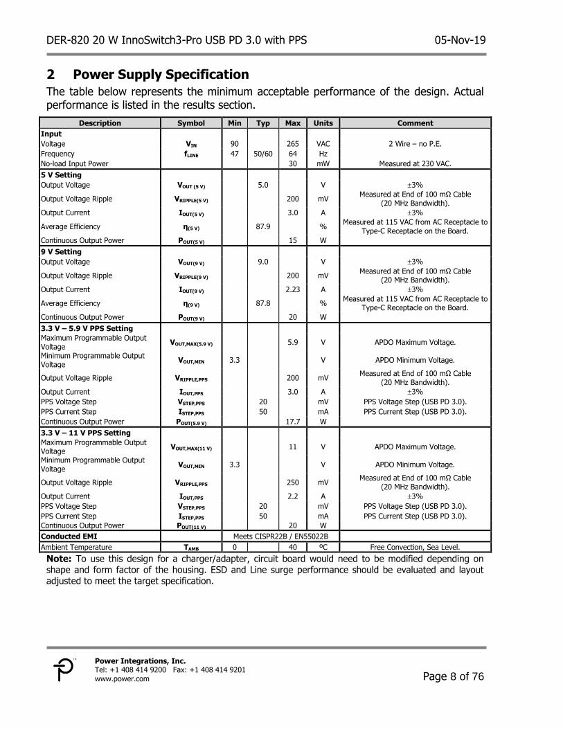
Power Supply Specification 2
The table below represents the minimum acceptable performance of the design. Actual performance is listed in the results section.
Description Symbol Min Typ Max Units Comment
Input
Voltage VIN 90 265 VAC 2 Wire – no P.E.
Frequency fLINE 47 50/60 64 Hz
No-load Input Power 30 mW Measured at 230 VAC.
5 V Setting
Output Voltage VOUT (5 V) 5.0 V 3%
Output Voltage Ripple VRIPPLE(5 V)
200 mV Measured at End of 100 mΩ Cable
(20 MHz Bandwidth).
Output Current IOUT(5 V) 3.0 A 3%
Average Efficiency ƞ(5 V) 87.9 % Measured at 115 VAC from AC Receptacle to
Type-C Receptacle on the Board.
Continuous Output Power POUT(5 V) 15 W
9 V Setting
Output Voltage VOUT(9 V) 9.0 V 3%
Output Voltage Ripple VRIPPLE(9 V) 200 mV Measured at End of 100 mΩ Cable
(20 MHz Bandwidth).
Output Current IOUT(9 V) 2.23 A 3%
Average Efficiency ƞ(9 V) 87.8 % Measured at 115 VAC from AC Receptacle to
Type-C Receptacle on the Board.
Continuous Output Power POUT(9 V) 20 W
3.3 V – 5.9 V PPS Setting
Maximum Programmable Output Voltage
VOUT,MAX(5.9 V) 5.9 V APDO Maximum Voltage.
Minimum Programmable Output Voltage
VOUT,MIN 3.3 V APDO Minimum Voltage.
Output Voltage Ripple VRIPPLE,PPS 200 mV Measured at End of 100 mΩ Cable
(20 MHz Bandwidth).
Output Current IOUT,PPS 3.0 A 3%
PPS Voltage Step VSTEP,PPS 20 mV PPS Voltage Step (USB PD 3.0).
PPS Current Step ISTEP,PPS 50 mA PPS Current Step (USB PD 3.0).
Continuous Output Power POUT(5.9 V) 17.7 W
3.3 V – 11 V PPS Setting
Maximum Programmable Output Voltage
VOUT,MAX(11 V) 11 V APDO Maximum Voltage.
Minimum Programmable Output Voltage
VOUT,MIN 3.3 V APDO Minimum Voltage.
Output Voltage Ripple VRIPPLE,PPS 250 mV Measured at End of 100 mΩ Cable
(20 MHz Bandwidth).
Output Current IOUT,PPS 2.2 A 3%
PPS Voltage Step VSTEP,PPS 20 mV PPS Voltage Step (USB PD 3.0).
PPS Current Step ISTEP,PPS 50 mA PPS Current Step (USB PD 3.0).
Continuous Output Power POUT(11 V) 20 W
Conducted EMI Meets CISPR22B / EN55022B
Ambient Temperature TAMB 0 40 ºC Free Convection, Sea Level.
Note: To use this design for a charger/adapter, circuit board would need to be modified depending on shape and form factor of the housing. ESD and Line surge performance should be evaluated and layout
adjusted to meet the target specification.
05-Nov-19 DER-820 20 W InnoSwitch3-Pro USB PD 3.0 with PPS
Page 9 of 76
Power Integrations Tel: +1 408 414 9200 Fax: +1 408 414 9201
www.power.com
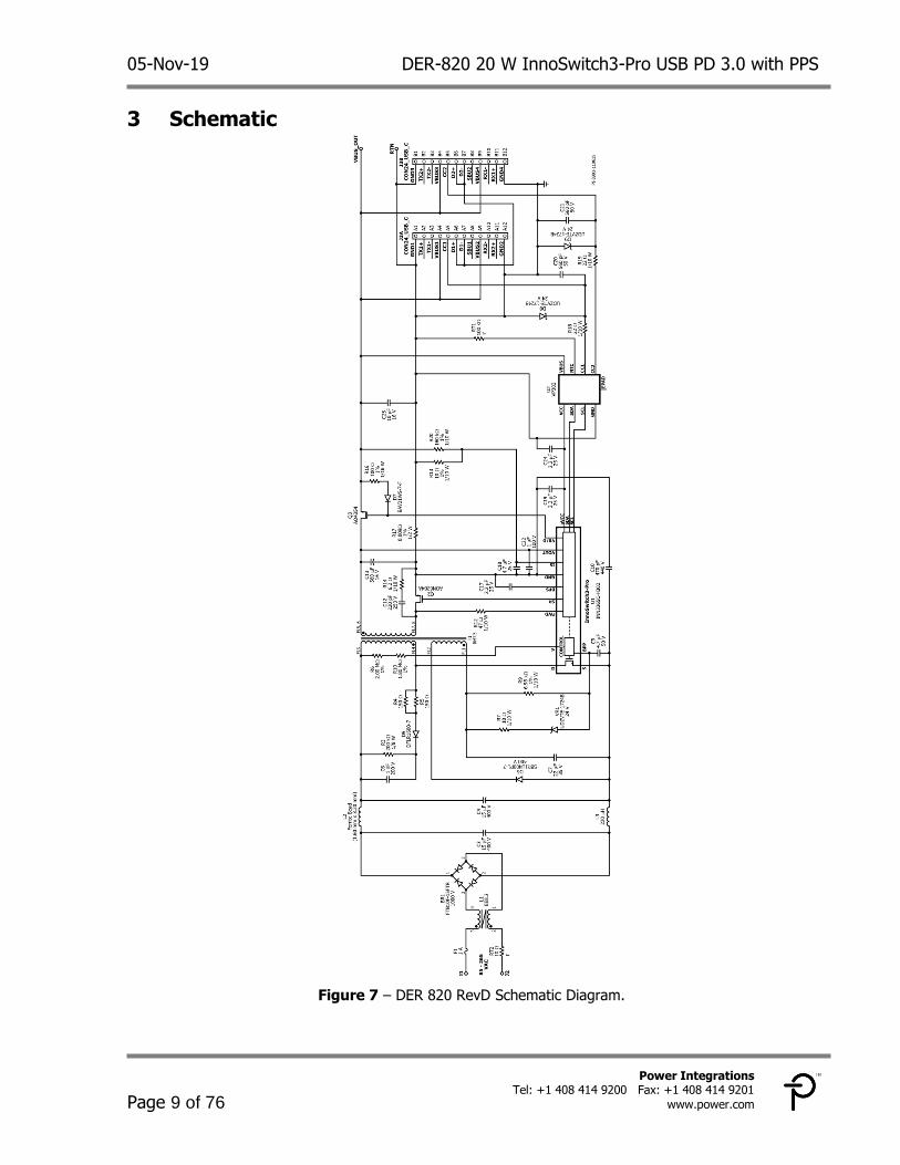
Schematic 3
Figure 7 – DER 820 RevD Schematic Diagram.
DER-820 20 W InnoSwitch3-Pro USB PD 3.0 with PPS 05-Nov-19
Page 10 of 76
Power Integrations, Inc. Tel: +1 408 414 9200 Fax: +1 408 414 9201 www.power.com
Circuit Description 4
Input Rectifier and EMI Filter 4.1
Fuse F1 isolates the circuit and provides protection from component failure. Common mode choke L1, inductors L2 and L3, and capacitor C10 provide common mode and differential mode noise filtering for EMI attenuation. Bridge rectifier BR1 rectifies the AC line voltage and provides a full wave rectified DC across C3 and C4.
InnoSwitch3-Pro IC Primary 4.2
One end of the transformer primary is connected to the rectified DC bus and the other end is connected to the drain terminal of the switch inside the InnoSwitch3-Pro IC U1. Resistors R6 and R10 provide input voltage sensing and undervoltage and overvoltage protection via the V pin of U1. A low-cost RCD clamp formed by diode D5, resistors R3, R4, R5 and capacitor C6 limits the peak drain-source voltage of U1 at the instant the switch inside U1 turns off. The clamp helps to dissipate the energy stored in the leakage reactance of transformer T1. The IC is self-starting, using an internal high-voltage current source to charge the BPP pin capacitor C9 when AC is first applied. During normal operation the primary-side block is powered from an auxiliary winding on the transformer T1. The output of the auxiliary (or bias) winding is rectified using diode D6 and filtered using capacitor C7. Resistor R9 limits the current being supplied to the BPP pin of the InnoSwitch3-Pro IC U1. The R9 value must be well selected to ensure a sufficient current flowing through R9 such that the internal current source of U1 is off during normal operation to reduce the no load input power. Zener diode VR1 offers primary sensed output overvoltage protection. In a flyback converter, output of the auxiliary winding tracks the output voltage of the converter. In case of overvoltage at output of the converter, the auxiliary winding voltage increases and causes the breakdown of VR1 resulting in excessive current to flow into the BPP pin of InnoSwitch3-Pro IC U1. If the current flowing into the BPP pin increases above the ISD threshold, the InnoSwitch3-Pro controller will latch off and prevent any further increase in output voltage. Resistor R7 limits the current injected to BPP pin during output overvoltage protection event.
InnoSwitch3-Pro IC Secondary and USB Power Delivery Controller 4.3
The secondary-side of the InnoSwitch3-Pro IC provides output voltage and current sensing and a gate drive to a FET for synchronous rectification. The voltage across the transformer secondary winding is rectified by the secondary-side FET (or SR FET) Q2 and filtered by capacitor C13. High frequency ringing during switching transients that would otherwise create radiated EMI is reduced via RC snubber R14 and C12.

05-Nov-19 DER-820 20 W InnoSwitch3-Pro USB PD 3.0 with PPS
Page 11 of 76
Power Integrations Tel: +1 408 414 9200 Fax: +1 408 414 9201
www.power.com
The gate of Q2 is turned on by secondary-side controller inside IC U1, based on the secondary winding voltage sensed via resistor R12 and fed into the FWD pin of the IC. In continuous conduction mode of operation, the SR FET is turned off just prior to the secondary-side commanding a new switching cycle from the primary. In discontinuous mode of operation, the SR FET is turned off when the magnitude of the voltage drop across the SR FET falls below a threshold of approximately VSR(TH). Secondary-side control of the primary-side power switch avoids any possibility of cross conduction of the two switches and provides extremely reliable synchronous rectifier operation. The secondary-side of the IC is self-powered from either the secondary winding forward voltage or the output voltage. Capacitor C17 connected to the BPS pin of InnoSwitch3-Pro IC U1 provides decoupling for the internal circuitry. The output current is sensed by monitoring the voltage drop across resistor R17. Resistors R13 and R20 add an offset to the sensed output current to provide a positive slope to the CC characteristic. The resulting current measurement is filtered with decoupling capacitor C18 and monitored across the IS and SECONDARY GROUND pins. An internal current sense threshold which is configured via the I2C interface up to approximately 32 mV is used to reduce losses. Once the threshold is exceeded, the InnoSwitch3-Pro IC U1 regulates the number of switch pulses to maintain a fixed output current. During constant current (CC) operation, when the output voltage falls, the secondary-side controller inside InnoSwitch3-Pro IC U1 will power itself from the secondary winding directly. During the on-time of the primary-side power switch, the forward voltage that appears across the secondary winding is used to charge the SECONDARY BYPASS pin decoupling capacitor C17 via resistor R12 and an internal regulator. This allows output current regulation to be maintained down to the minimum UV threshold. Below this level the unit enters auto-restart until the output load is reduced. When the output current is below the CC threshold, the converter operates in constant voltage mode. The output voltage is monitored by the VOUT pin of the InnoSwitch3-Pro IC. Similar with current regulation, the output voltage is also compared to an internal voltage threshold that is set via the I2C interface and the controller inside IC U1 regulates the output voltage by controlling the number of switch pulses. Capacitor C22 is needed between the VOUT pin and the SECONDARY GROUND pin for ESD protection of the VOUT pin. N-channel MOSFET Q3 functions as the bus switch which connects or disconnects the output of the flyback converter from the USB Type-C receptacle. Q3 is controlled by the VB/D pin on the InnoSwitch3-Pro IC. Resistor R16 and diode D7 are connected across the Source and Gate terminals of the Q3 to provide a discharge path for the bus voltage
DER-820 20 W InnoSwitch3-Pro USB PD 3.0 with PPS 05-Nov-19
Page 12 of 76
Power Integrations, Inc. Tel: +1 408 414 9200 Fax: +1 408 414 9201 www.power.com
when the Q3 is turned off. Capacitors C16 and C25 are used at the output for ESD protection. In this design, VP302 (U2) is the USB Power Delivery (USB PD) controller. It is powered by the InnoSwitch3-Pro IC through the µVCC pin. USB PD protocol is communicated over either CC1 or CC2 line depending on the orientation in which Type-C plug is connected. The VP302 IC communicates with InnoSwitch3-Pro IC through the I2C interface using the SCL and SDA lines in which it sets the CV, CC, VKP, OVA and UVA parameters. These parameters correspond to the output voltage, constant output current, constant output power voltage threshold, output overvoltage threshold, and output undervoltage threshold registers of the InnoSwitch3-Pro IC, respectively. The status of the InnoSwitch3-Pro IC is read by the VP302 IC from the telemetry registers also using the I2C interface. Capacitors C19 and C24 provide decoupling to the µVCC of the InnoSwitch3-Pro IC and VCC of the VP302 IC. Capacitors C20 and C21, resistors R18 and R19, and TVS diodes D8, and D9 provide protection from ESD to pins CC1 and CC2. Thermistor RT1 is connected to NTC pin of the VP302 IC to provide temperature detection of the USB Type-C receptacle. The VBUS pin of the VP302 IC is used to sense the output voltage at the USB Type-C receptacle, which is the voltage after the bus switch Q3. The VBUS pin is also used for discharging the capacitors C16 and C25 when the bus switch Q3 is opened.
05-Nov-19 DER-820 20 W InnoSwitch3-Pro USB PD 3.0 with PPS
Page 13 of 76
Power Integrations Tel: +1 408 414 9200 Fax: +1 408 414 9201
www.power.com
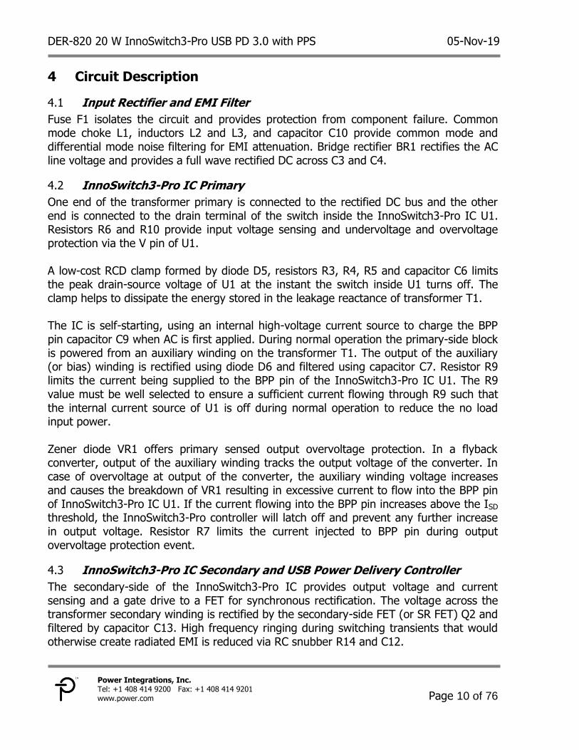
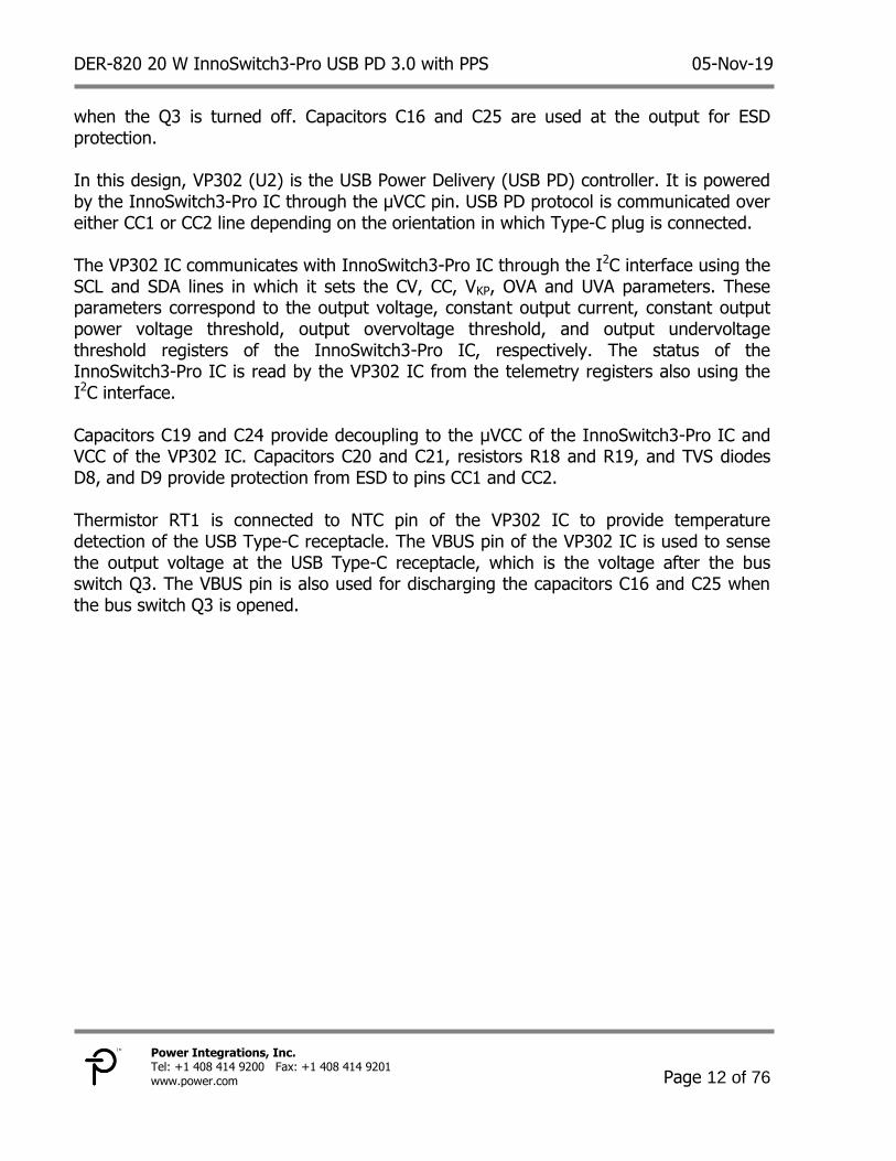
PCB Layout 5
PCB copper thickness is 0.062 inches.
Figure 8 – Motherboard Printed Circuit Layout, Top.
Figure 9 – Motherboard Printed Circuit Layout, Bottom.
DER-820 20 W InnoSwitch3-Pro USB PD 3.0 with PPS 05-Nov-19
Page 14 of 76
Power Integrations, Inc. Tel: +1 408 414 9200 Fax: +1 408 414 9201 www.power.com
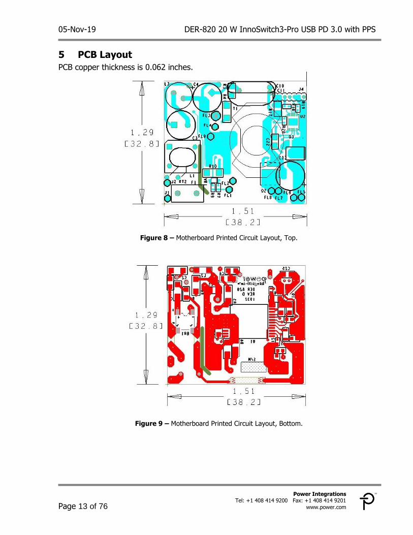
Figure 10 – Daughterboard Printed Circuit Layout, Top.
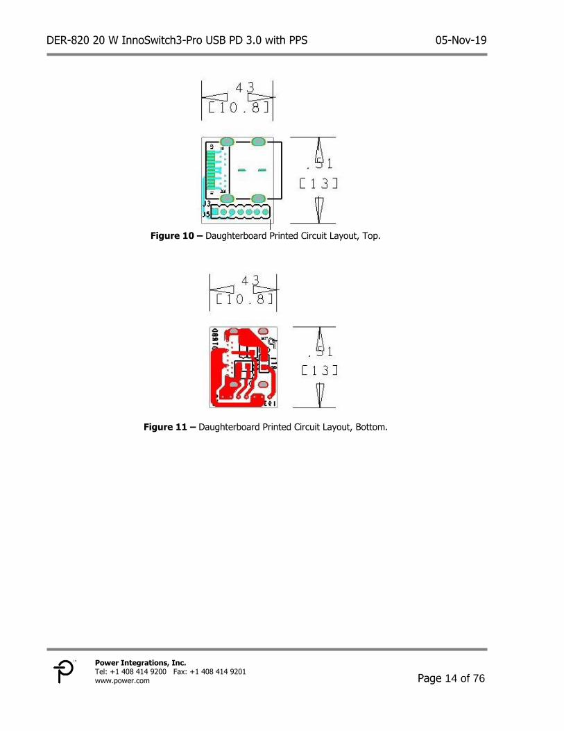
Figure 11 – Daughterboard Printed Circuit Layout, Bottom.

05-Nov-19 DER-820 20 W InnoSwitch3-Pro USB PD 3.0 with PPS
Page 15 of 76
Power Integrations Tel: +1 408 414 9200 Fax: +1 408 414 9201
www.power.com
Bill of Materials 6Item Part Ref Qty Description Mfg Part Number Mfg
1 BR1 1 BRIDGE RECT, 1PH, 1KV, 1.5A, 4-SMD FTB10F-15FTR SMC Diode
2 C3 C4 2 15 F, 400 V, Electrolytic, (8 x 16)
3 C6 1 1 nF, 200 V, Ceramic, X7R, 0805 08052C102KAT2A AVX
4 C7 1 22 F, 35 V, Ceramic, X5R, 1206 C3216X5R1V226M160AC TDK
5 C9 1 4.7 F, 50 V, Ceramic, X5R, 0805 CL21A475KBQNNNE Samsung
6 C10 1 470 pF, ±10%, 440 VAC, (X1, Y2) rated, Ceramic, Y5S, Radial, Disc, -40°C ~ 125°C
VY2471K29Y5SS63V7 Vishay
7 C12 1 220 pF, 250 V, Ceramic, COG, 0603 C1608C0G2E221J TDK
8 C13 1 560 F, 16 V, Al Organic Polymer, Gen. Purpose,
20% APSG160ELL561MHB5J United Chemi-con
9 C17 C19 2 2.2 F, 25 V, Ceramic, X7R, 0805 C2012X7R1E225M TDK
10 C18 1 4.7 F ±10%, 25V, X7R, 0805, 55°C ~ 125°C TMK212AB7475KG-T Taiyo Yuden
11 C20 C21 2 560 pF, 50V, Ceramic, X7R, 0603, 0.063" L x 0.031" W (1.60 mm x 0.80 mm)
CL10B561KB8NNNC Samsung
12 C22 1 1 F, 100 V, Ceramic, X7S, 0805 C2012X7S2A105K125AB TDK
13 C24 1 2.2 F, ±10%, 25 V, Ceramic, X7R, 0603, -55 to 125 °C
GRM188Z71E225KE43D Murata
14 C25 1 10 F, 16 V, Ceramic, X5R, 0805 GRM21BR61C106KE15L Murata
15 D5 1 600 V, 1 A, Rectifier, Glass Passivated, POWERDI123 DFLR1600-7 Diodes, Inc.
16 D6 1 DIODE, SBR, 400 V, 1 A, POWERDI123,PowerDI™ 123
SBR1U400P1-7 Diodes, Inc.
17 D7 1 250 V, 0.2 A, Fast Switching, 50 ns, SOD-323 BAV21WS-7-F Diodes, Inc.
18 D8 D9 VR1
3 DIODE, ZENER, 24 V, 200 mW, UMD2, SOD323F,SC-90, SOD-323F
UDZVTE-1724B Rohm
19 F1 1 1 A, 250 V, Slow, Long Time Lag, RST 1 RST 1 Belfuse
20 J3 1 Connector, "Certified", USB - C, USB 3.1, For 0.062" PCB Material!, Superspeed+, Receptacle Connector, 24 Position, SMT, RA, TH
632723300011 Wurth
21 L1 1 Bobbin, EE8.3, Horizontal, 4 pins (8.2mm W x 8.3mm L x 7.6mm H)
EE-8.3 Shenzhen
Jinshengxin Tech
22 L2 1 Ferrite Bead, 220 , 0.3A, 1206 SMD 742792122 Wurth
23 L3 1 Inductor, Fixed, 220 H 0.43A 5.4MHz, Radial Lead 22R224C Murata
24 Q2 1 MOSFET, N-Channel, 80V, 48A (Tc), 56W (Tc), Surface Mount, 8DFN,8-DFN-EP (5x6)
AON6284A Alpha & Omega
Semi
25 Q3 1 MOSFET, N-CH, 30V, 23A (Ta), 3.1W (Ta),3.7 mOhm (@ 20A, 10V), 8SOIC
AO4354 Alpha & Omega
Semi
26 R3 1 RES, 200 k, 5%, 1/8 W, Automotive, AEC-Q200,
Thick Film, 0805 ERJ-6GEYJ204V Panasonic
27 R4 R5 2 RES, 150 , 5%, 1/4 W, Automotive, AEC-Q200, Thick Film, 1206
ERJ-8GEYJ151V Panasonic
28 R6 1 RES, 2.00 M, 1%, 1/4 W, Thick Film, 1206 ERJ-8ENF2004V Panasonic
29 R7 1 RES, 10 , 5%, 1/10 W, Automotive, AEC-Q200,
Thick Film, 0402 ERJ-2GEJ100X Panasonic
30 R9 1 RES, 6.98 k, 1%, 1/10 W, Automotive, AEC-Q200,
Thick Film, 0402 ERJ-2RKF6981X Panasonic
31 R10 1 RES, 1.80 M, 1%, 1/4 W, Thick Film, 1206 ERJ-8ENF1804V Panasonic
32 R12 1 RES, 47 , 5%, 1/10 W, Automotive, AEC-Q200,
Thick Film, 0402 ERJ-2GEJ470X Panasonic
33 R13 1 RES, 10 , 1%, 1/10 W, Automotive, AEC-Q200,
Thick Film, 0402 ERJ-2RKF10R0X Panasonic
34 R14 1 RES, 6.2 , 5%, 1/10 W, Automotive, AEC-Q200,
Thick Film, 0603 ERJ-3GEYJ6R2V Panasonic
35 R16 1 RES, 100 , 1%, 1/16 W, Automotive, AEC-Q200, Thick Film, 0603
ERJ-3EKF1000V Panasonic
36 R17 1 RES, 0.009 , ±1%, 0.5 W, 0805, Automotive AEC-
Q200, Current Sense, Moisture Resistant, Metal Element
CRF0805-FZ-R009ELF Bourns

DER-820 20 W InnoSwitch3-Pro USB PD 3.0 with PPS 05-Nov-19
Page 16 of 76
Power Integrations, Inc. Tel: +1 408 414 9200 Fax: +1 408 414 9201 www.power.com
37 R18 R19 2 RES, 22 , 5%, 1/10 W, Automotive, AEC-Q200, Thick Film, 0402
ERJ-2GEJ220X Panasonic
38 R20 1 RES, 160.0 k, 1%, 1/10 W, Automotive, AEC-
Q200, Thick Film, 0402 ERJ-2RKF1603X Panasonic
39 RT1 1 NTC Thermistor, 100 k, 3%, 0603 NCP18WF104E03RB Murata
40 RT2 1 NTC Thermistor, 10 , 0.7 A MF72-010D5 Cantherm
41 T1 1 Bobbin, EP13, Vertical, 5 pins RM-7.5-1 Shen Zhen Xin Yu
Jia Tech
42 U1 1 InnoSwitch3-Pro, InSOP24D INN3365C-H302 Power
Integrations
43 U2 1 IC, USB PD Type-C Controller for SMPS, DFN-8 VP302 VIA Labs

05-Nov-19 DER-820 20 W InnoSwitch3-Pro USB PD 3.0 with PPS
Page 17 of 76
Power Integrations Tel: +1 408 414 9200 Fax: +1 408 414 9201
www.power.com
Transformer Specification 7
Electrical Diagram 7.1
Figure 12 – Transformer Electrical Diagram.
Electrical Specifications 7.2
Parameter Condition Spec.
Primary
Inductance
Measured at 1 VPK-PK, 100 kHz switching frequency, between FL3 and
FL4, with all other windings open. 494 H ±5%
Primary Leakage
Inductance
Measured at 1 VPK-PK, 100 kHz switching frequency, between FL3 and
FL4, with shorted bias (FL1 to FL2) and secondary (FL5,6 to FL7,8) windings.
10 H (Max).
Material List 7.3
Item Description
[1] Core: RM7.5, ACP47 Material.
[2] Bobbin: RM7.5 Vertical, 5pins, PI custom, P/N: 25-01113-00.
[3] Magnet Wire: #28 AWG, Double Coated.
[4] Magnet Wire: #30 AWG, Double Coated.
[5] Magnet Wire: #32 AWG, Double Coated.
[6] Magnet Wire: #23 AWG, Triple Insulated Wire.
[7] Bus Wire: #26 AWG, Alpha Wire, Tinned Copper.
[8] Tape: 3M 1350F-1, Polyester Film, 1 mil Thickness, 6.8 mm Width.
[9] Tape: 3M 1350F-1, Polyester Film, 1 mil Thickness, 20 mm Width.
[10] Tape: 3M 1350F-1, Polyester Film, 1 mil Thickness, 4.5 mm Width.
[11] Varnish: Dolph BC-359 or Equivalent.
FL4
FL2
FL1
FL5,6
FL7,8
WD4 (Secondary): 4T – 2× #23AWG_TIW
WD3 (Bias): 8T – 2× #30 AWG
WD1 (Primary1) 18T – #28AWG
#26 AWG-bus wire
WD6 (Primary2) 18T – #28AWG
FL3
WD5 (Shield2) 5T – 4T× #32AWG
NC
WD2 (Shield1): 5T – #30 AWG
NC
FL3
FL9

DER-820 20 W InnoSwitch3-Pro USB PD 3.0 with PPS 05-Nov-19
Page 18 of 76
Power Integrations, Inc. Tel: +1 408 414 9200 Fax: +1 408 414 9201 www.power.com
Transformer Build Diagram 7.4
FL4
FL3
FL2
WD1 (Primary) 18T - #28AWG
WD4 (Secondary): 4T – 2× #23AWG_TIW
1TFL1
2T
FL5,6
WD3 (Bias): 8T –2× #30 AWG
FL7,8
WD5 (Shield2): 5T – 4× #32AWGEqually Distributed
NC
NCWD2 (Shield1): 5T – #30 AWG
WD6 (Primary) 18T – #28AWG
FL32T
1T
5
5
Figure 13 – Transformer Build Diagram.
Transformer Construction 7.5
Winding Directions Bobbin is oriented on winder jig such that Pin 1 through Pin 4 are on the left side.
The winding direction is clockwise.
WD1 1st Half Primary
Use magnetic wire, Item [3]. Mark starting end as FL4. Start at temporary pin and wind 18 turns from left to right. Finish the winding on pin 5.
Insulation Apply 1 layer of polyester tape, Item [8] for insulation
WD2, WD3
Shield1 and Bias
(wind in parallel)
Use magnetic wire, Item [4]. WD2 and WD3 are wound in parallel. Combine the 3
wires and mark starting end as FL1. Start at temporary pin and wind 5 trifilar turns. Stop winding WD2 at this point and terminate a single wire. Wind the remaining 3
bifilar turns for WD3. Pull WD3 wires back to left and mark the end of WD3 as FL2
Insulation Apply 2 layer of polyester tape, Item [8] for insulation
WD4
Secondary
Use magnetic wire, Item [6]. Mark starting end as FL5,6. Start at left on the
secondary-side of the bobbin. Wind 4 bifilar turns and terminate on the right side of the bobbin. Mark end as FL7,8
Insulation Apply 2 layer of polyester tape, Item [8] for insulation
WD5
Shield2
Use magnetic wire, Item [5]. Mark starting end as FL3. Start at temporary pin and
wind 5 quadfilar turns. Terminate as no connection (NC)
Insulation Apply 1 layer of polyester tape, Item [8] for insulation
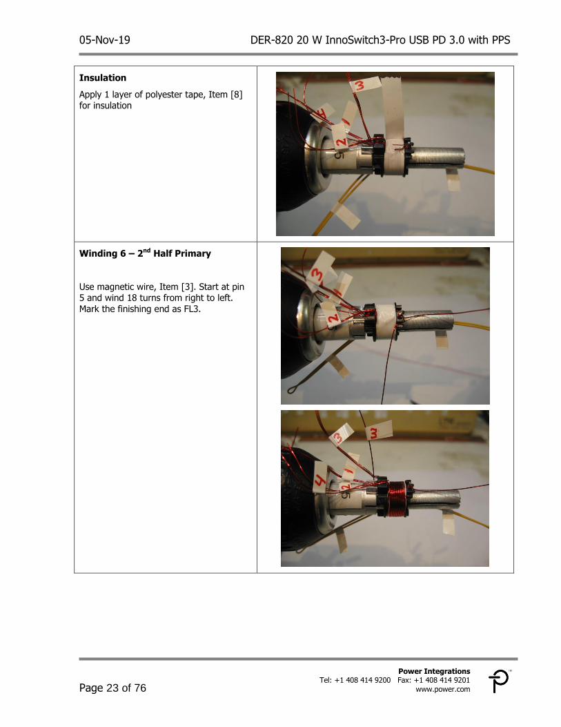
WD6
2nd Half Primary
Use magnetic wire, Item [3]. Start at pin 5 and wind 18 turns from right to left.
Mark the finishing end as FL3.
Insulation Apply 2 layer of polyester tape, Item [8] for insulation
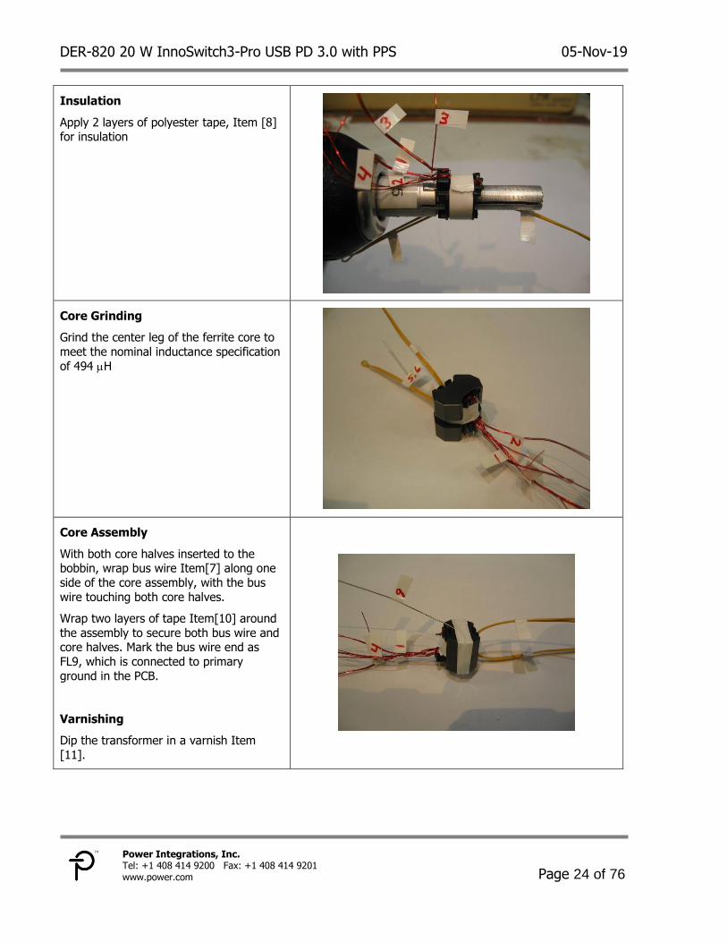
Core Grinding Grind the center leg of the ferrite core to meet the nominal inductance specification
of 494 H.
Core Assembly
With both core halves inserted to the bobbin, wrap bus wire Item [7] along one side
of the core assembly, with the bus wire touching both core halves. Wrap two layers of tape Item [10] around the assembly to secure both bus wire and
core halves. Mark the bus wire end as FL9, which is connected to primary ground in the PCB.
Varnishing Dip the transformer in a varnish.
Safety Insulation
Tape
Cut off pins 1 to 4. Apply 2 layers safety insulation tape Item [9] to cover the bottom and sides of the core. Ensure the bottom part is completely covered with
tape. Wrap another 1 layer of tape Item [8] around the transformer sides to secure the assembly.
05-Nov-19 DER-820 20 W InnoSwitch3-Pro USB PD 3.0 with PPS
Page 19 of 76
Power Integrations Tel: +1 408 414 9200 Fax: +1 408 414 9201
www.power.com
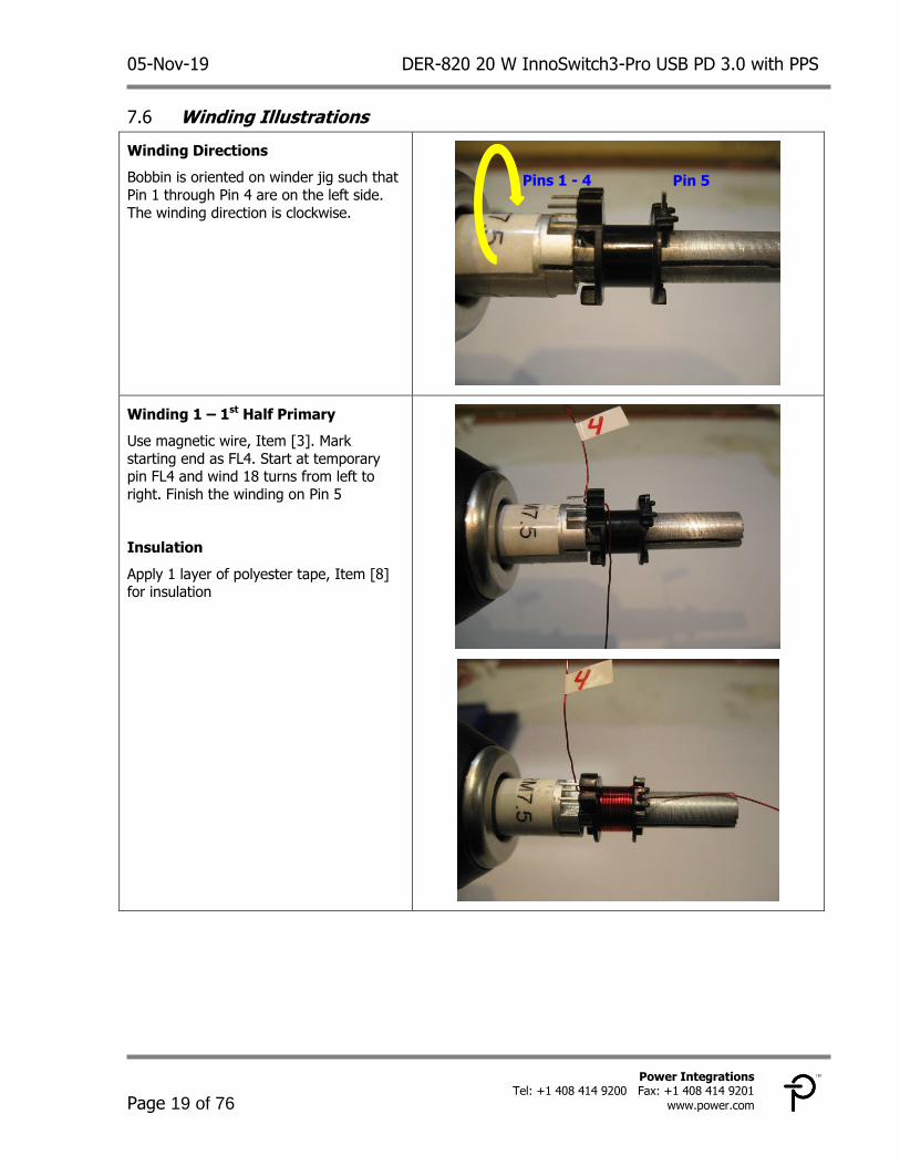
Winding Illustrations 7.6
Winding Directions
Bobbin is oriented on winder jig such that
Pin 1 through Pin 4 are on the left side.
The winding direction is clockwise.
Winding 1 – 1st Half Primary
Use magnetic wire, Item [3]. Mark
starting end as FL4. Start at temporary pin FL4 and wind 18 turns from left to
right. Finish the winding on Pin 5
Insulation
Apply 1 layer of polyester tape, Item [8] for insulation
Pin 5 Pins 1 - 4
DER-820 20 W InnoSwitch3-Pro USB PD 3.0 with PPS 05-Nov-19
Page 20 of 76
Power Integrations, Inc. Tel: +1 408 414 9200 Fax: +1 408 414 9201 www.power.com
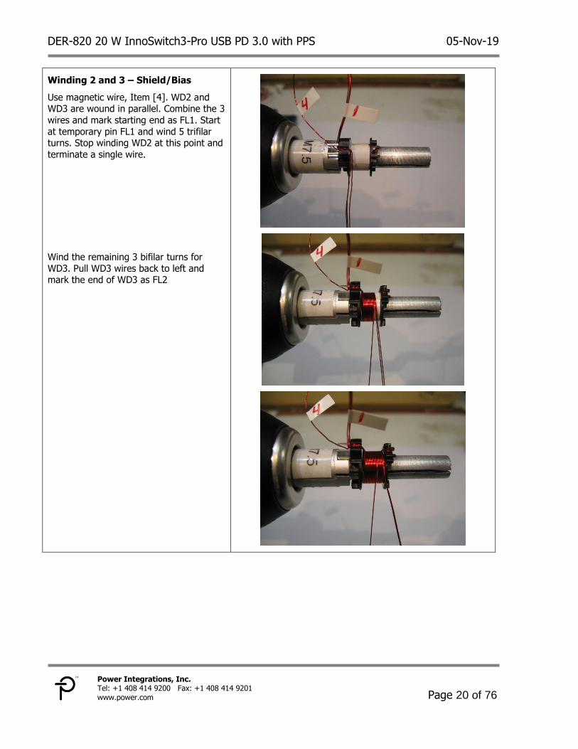
Winding 2 and 3 – Shield/Bias
Use magnetic wire, Item [4]. WD2 and WD3 are wound in parallel. Combine the 3
wires and mark starting end as FL1. Start
at temporary pin FL1 and wind 5 trifilar turns. Stop winding WD2 at this point and
terminate a single wire.
Wind the remaining 3 bifilar turns for
WD3. Pull WD3 wires back to left and mark the end of WD3 as FL2

05-Nov-19 DER-820 20 W InnoSwitch3-Pro USB PD 3.0 with PPS
Page 21 of 76
Power Integrations Tel: +1 408 414 9200 Fax: +1 408 414 9201
www.power.com
Insulation
Apply 2 layer of polyester tape, Item [8] for insulation
Winding 4 - Secondary Winding
Use magnetic wire, Item [6]. Mark
starting end as FL5,6. Start at left on the
secondary-side of the bobbin. Wind 4 bifilar turns and terminate on the right
side of the bobbin. Mark end as FL7,8

DER-820 20 W InnoSwitch3-Pro USB PD 3.0 with PPS 05-Nov-19
Page 22 of 76
Power Integrations, Inc. Tel: +1 408 414 9200 Fax: +1 408 414 9201 www.power.com
Insulation
Apply 2 layer of polyester tape, Item [8] for insulation
Winding 5 - Shield Winding
Use magnetic wire, Item [5]. Mark
starting end as FL3. Start at temporary
pin FL3 and wind 5 quad filar turns. Terminate as no connection (NC).
05-Nov-19 DER-820 20 W InnoSwitch3-Pro USB PD 3.0 with PPS
Page 23 of 76
Power Integrations Tel: +1 408 414 9200 Fax: +1 408 414 9201
www.power.com
Insulation
Apply 1 layer of polyester tape, Item [8] for insulation
Winding 6 – 2nd Half Primary
Use magnetic wire, Item [3]. Start at pin 5 and wind 18 turns from right to left.
Mark the finishing end as FL3.
DER-820 20 W InnoSwitch3-Pro USB PD 3.0 with PPS 05-Nov-19
Page 24 of 76
Power Integrations, Inc. Tel: +1 408 414 9200 Fax: +1 408 414 9201 www.power.com
Insulation
Apply 2 layers of polyester tape, Item [8] for insulation
Core Grinding
Grind the center leg of the ferrite core to
meet the nominal inductance specification
of 494 H
Core Assembly
With both core halves inserted to the bobbin, wrap bus wire Item[7] along one
side of the core assembly, with the bus
wire touching both core halves.
Wrap two layers of tape Item[10] around
the assembly to secure both bus wire and core halves. Mark the bus wire end as
FL9, which is connected to primary
ground in the PCB.
Varnishing
Dip the transformer in a varnish Item
[11].

05-Nov-19 DER-820 20 W InnoSwitch3-Pro USB PD 3.0 with PPS
Page 25 of 76
Power Integrations Tel: +1 408 414 9200 Fax: +1 408 414 9201
www.power.com
Safety Insulation Tape
Cut off pins 1 to 4. Apply 2 layers safety insulation tape Item[9] to cover the
bottom and sides of the core.
Ensure the bottom part is completely
covered with tape.
Wrap another 1 layer of tape Item[8]
around the transformer sides to secure the assembly.

DER-820 20 W InnoSwitch3-Pro USB PD 3.0 with PPS 05-Nov-19
Page 26 of 76
Power Integrations, Inc. Tel: +1 408 414 9200 Fax: +1 408 414 9201 www.power.com
Common Mode Choke Specifications 8
6.3 mH Common Mode Choke (L1) 8.1
Electrical Diagram 8.1.1
2
1
3
4
42T - #30AWG 42T - #30AWG
Figure 14 – Inductor Electrical Diagram.
Electrical Specifications 8.1.2
Winding Inductance
Pin 1 – pin 2 (or pin 3 – pin 4), all other windings open, measured at 100 kHz, 0.4 VRMS.
6.3 mH (Min.)
Primary
Leakage
Between pin 1 and pin 2, with pin 3 and pin 4 shorted. 45 H
Material List 8.1.3
Item Description
[1] Core: EE8.3.
[2] Bobbin: EE8.3-H-4pins (2/2); PI: 25-01080-00.
[3] Magnet Wire: #30 AWG, Double Coated.
[4] Tape: 3M 1350-F, Polyester Film, 1 mil Thickness, 3.0 mm Width.
[5] Varnish: Dolph BC-359 or Equivalent.
Inductor Build Diagram 8.1.4
1
2 3
4
42T - #30AWG 42T - #30AWG
Figure 15 – Inductor Build Diagram.

05-Nov-19 DER-820 20 W InnoSwitch3-Pro USB PD 3.0 with PPS
Page 27 of 76
Power Integrations Tel: +1 408 414 9200 Fax: +1 408 414 9201
www.power.com
Common Mode Choke Construction 8.1.5
Start as pin 1 wind 42 turns of Item [3] from left
to right finish as pin 2.
Start as pin 4 wind 42 turns of item [3] from right
to left and finish as pin 3.
Gap core halves to get 6.3 mH inductance (make sure to get 6.3-7.0 mH before varnish).
Place 2 layers tape of item [4] along the core.
Varnish item [5].
1
2 3
4
4
3

DER-820 20 W InnoSwitch3-Pro USB PD 3.0 with PPS 05-Nov-19
Page 28 of 76
Power Integrations, Inc. Tel: +1 408 414 9200 Fax: +1 408 414 9201 www.power.com
Transformer Design Spreadsheet 9
1
ACDC_InnoSwitch3-Pro_Flyback_081518; Rev.1.1; Copyright Power Integrations 2018
INPUT INFO OUTPUT UNITS InnoSwitch3-Pro Flyback Design Spreadsheet
2 APPLICATION VARIABLES
3 VAC_MIN 90
90 V Minimum AC line voltage
4 VAC_MAX 265
265 V Maximum AC input voltage
5 VAC_RANGE
UNIVERSAL
AC line voltage range
6 FLINE 47
47 Hz AC line voltage frequency
7 CAP_INPUT 24.0
24.0 uF Input capacitance
9 SETPOINT 1
10 VOUT1 9.00
9.05 V Output voltage 1, should be the highest output voltage required
11 IOUT1 2.230
2.230 A Output current 1
12 POUT1
20.18 W Output power 1
13 EFFICIENCY1 0.90
0.90
Converter efficiency for output 1
14 Z_FACTOR1 0.50
0.50
Z-factor for output 1
16 SETPOINT 2
17 VOUT2 5.00
5.07 V Output voltage 2
18 IOUT2 3.000
3.000 A Output current 2
19 POUT2
15.20 W Output power 2
20 EFFICIENCY2 0.87
0.87
Converter efficiency for output 2
21 Z_FACTOR2 0.50
0.50
Z-factor for output 2
23 SETPOINT 3
24 VOUT3
0.00 V Output voltage 3
25 IOUT3
0.000 A Output current 3
26 POUT3
0.00 W Output power 3
27 EFFICIENCY3
0.00
Converter efficiency for output 3
28 Z_FACTOR3
0.00
Z-factor for output 3
30 SETPOINT 4
31 VOUT4
0.00 V Output voltage 4
32 IOUT4
0.000 A Output current 4
33 POUT4
0.00 W Output power 4
34 EFFICIENCY4
0.00
Converter efficiency for output 4
35 Z_FACTOR4
0.00
Z-factor for output 4
37 SETPOINT 5
38 VOUT5
0.00 V Output voltage 5
39 IOUT5
0.000 A Output current 5
40 POUT5
0.00 W Output power 5
41 EFFICIENCY5
0.00
Converter efficiency for output 5
42 Z_FACTOR5
0.00
Z-factor for output 5
44 SETPOINT 6
45 VOUT6
0.00 V Output voltage 6
46 IOUT6
0.000 A Output current 6
47 POUT6
0.00 W Output power 6
48 EFFICIENCY6
0.00
Converter efficiency for output 6
49 Z_FACTOR6
0.00
Z-factor for output 6
51 SETPOINT 7
52 VOUT7
0.00 V Output voltage 7
53 IOUT7
0.000 A Output current 7
54 POUT7
0.00 W Output power 7
55 EFFICIENCY7
0.00
Converter efficiency for output 7
56 Z_FACTOR7
0.00
Z-factor for output 7
58 SETPOINT 8
59 VOUT8
0.00 V Output voltage 8
60 IOUT8
0.000 A Output current 8
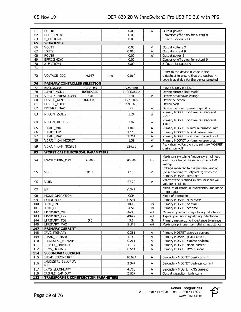
05-Nov-19 DER-820 20 W InnoSwitch3-Pro USB PD 3.0 with PPS
Page 29 of 76
Power Integrations Tel: +1 408 414 9200 Fax: +1 408 414 9201
www.power.com
61 POUT8
0.00 W Output power 8
62 EFFICIENCY8
0.00
Converter efficiency for output 8
63 Z_FACTOR8
0.00
Z-factor for output 8
65 SETPOINT 9
66 VOUT9
0.00 V Output voltage 9
67 IOUT9
0.000 A Output current 9
68 POUT9
0.00 W Output power 9
69 EFFICIENCY9
0.00
Converter efficiency for output 9
70 Z_FACTOR9
0.00
Z-factor for output 9
71
72 VOLTAGE_CDC 0.067 Info 0.067
Refer to the device H-code in the datasheet to ensure that the desired H-code is available for the device selected
76 PRIMARY CONTROLLER SELECTION
77 ENCLOSURE ADAPTER
ADAPTER
Power supply enclosure
78 ILIMIT_MODE INCREASED
INCREASED
Device current limit mode
79 VDRAIN_BREAKDOWN 650
650 V Device breakdown voltage
80 DEVICE_GENERIC INN33X5
INN33X5
Device selection
81 DEVICE_CODE
INN3365C
Device code
82 PDEVICE_MAX
22 W Device maximum power capability
83 RDSON_25DEG
2.24 Ω Primary MOSFET on-time resistance at 25°C
84 RDSON_100DEG
3.47 Ω Primary MOSFET on-time resistance at 100°C
85 ILIMIT_MIN
1.046 A Primary MOSFET minimum current limit
86 ILIMIT_TYP
1.150 A Primary MOSFET typical current limit
87 ILIMIT_MAX
1.254 A Primary MOSFET maximum current limit
88 VDRAIN_ON_MOSFET
1.32 V Primary MOSFET on-time voltage drop
89 VDRAIN_OFF_MOSFET
524.31 V Peak drain voltage on the primary MOSFET during turn-off
93 WORST CASE ELECTRICAL PARAMETERS
94 FSWITCHING_MAX 90000
90000 Hz Maximum switching frequency at full load and the valley of the minimum input AC voltage
95 VOR 81.0
81.0 V Voltage reflected to the primary winding (corresponding to setpoint 1) when the primary MOSFET turns off
96 VMIN
57.29 V Valley of the rectified minimum input AC voltage at full load
97 KP
0.746
Measure of continuous/discontinuous mode of operation
98 MODE_OPERATION
CCM
Mode of operation
99 DUTYCYCLE
0.591
Primary MOSFET duty cycle
100 TIME_ON
10.06 us Primary MOSFET on-time
101 TIME_OFF
4.54 us Primary MOSFET off-time
102 LPRIMARY_MIN
469.5 uH Minimum primary magnetizing inductance
103 LPRIMARY_TYP
494.2 uH Typical primary magnetizing inductance
104 LPRIMARY_TOL 5.0
5.0 % Primary magnetizing inductance tolerance
105 LPRIMARY_MAX
518.9 uH Maximum primary magnetizing inductance
107 PRIMARY CURRENT
108 IAVG_PRIMARY
0.381 A Primary MOSFET average current
109 IPEAK_PRIMARY
1.189 A Primary MOSFET peak current
110 IPEDESTAL_PRIMARY
0.261 A Primary MOSFET current pedestal
111 IRIPPLE_PRIMARY
1.132 A Primary MOSFET ripple current
112 IRMS_PRIMARY
0.551 A Primary MOSFET RMS current
114 SECONDARY CURRENT
115 IPEAK_SECONDARY
10.699 A Secondary MOSFET peak current
116 IPEDESTAL_SECONDARY
2.347 A Secondary MOSFET pedestal current
117 IRMS_SECONDARY
4.705 A Secondary MOSFET RMS current
118 IRIPPLE_CAP_OUT
3.624 A Output capacitor ripple current
122 TRANSFORMER CONSTRUCTION PARAMETERS
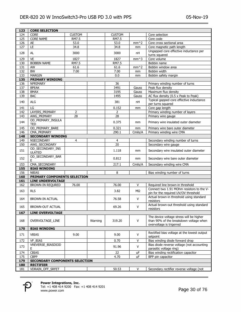
DER-820 20 W InnoSwitch3-Pro USB PD 3.0 with PPS 05-Nov-19
Page 30 of 76
Power Integrations, Inc. Tel: +1 408 414 9200 Fax: +1 408 414 9201 www.power.com
123 CORE SELECTION
124 CORE CUSTOM
CUSTOM
Core selection
125 CORE NAME RM7.5
RM7.5
Core code
126 AE 53.0
53.0 mm^2 Core cross sectional area
127 LE 34.8
34.8 mm Core magnetic path length
128 AL 3000
3000 nH Ungapped core effective inductance per turns squared
129 VE 1827
1827 mm^3 Core volume
130 BOBBIN NAME RM7.5
RM7.5
Bobbin name
131 AW 61.6
61.6 mm^2 Bobbin window area
132 BW 7.00
7.00 mm Bobbin width
133 MARGIN
0.0 mm Bobbin safety margin
135 PRIMARY WINDING
136 NPRIMARY
36
Primary winding number of turns
137 BPEAK
3491 Gauss Peak flux density
138 BMAX
3195 Gauss Maximum flux density
139 BAC
1495 Gauss AC flux density (0.5 x Peak to Peak)
140 ALG
381 nH Typical gapped core effective inductance per turns squared
141 LG
0.152 mm Core gap length
142 LAYERS_PRIMARY 2
2
Primary winding number of layers
143 AWG_PRIMARY 28
28
Primary wire gauge
144 OD_PRIMARY_INSULATED
0.375 mm Primary wire insulated outer diameter
145 OD_PRIMARY_BARE
0.321 mm Primary wire bare outer diameter
146 CMA_PRIMARY
290.1 Cmils/A Primary winding wire CMA
148 SECONDARY WINDING
149 NSECONDARY 4
4
Secondary winding number of turns
150 AWG_SECONDARY
20
Secondary wire gauge
151 OD_SECONDARY_INSULATED
1.118 mm Secondary wire insulated outer diameter
152 OD_SECONDARY_BARE
0.812 mm Secondary wire bare outer diameter
153 CMA_SECONDARY
217.1 Cmils/A Secondary winding wire CMA
155 BIAS WINDING
156 NBIAS
8
Bias winding number of turns
160 PRIMARY COMPONENTS SELECTION
161 LINE UNDERVOLTAGE
162 BROWN-IN REQURED 76.00
76.00 V Required line brown-in threshold
163 RLS
3.82 MΩ Connect two 1.91 MOhm resistors to the V-pin for the required UV/OV threshold
164 BROWN-IN ACTUAL
76.58 V Actual brown-in threshold using standard resistors
165 BROWN-OUT ACTUAL
69.26 V Actual brown-out threshold using standard resistors
167 LINE OVERVOLTAGE
168 OVERVOLTAGE_LINE
Warning 319.20 V The device voltage stress will be higher than 90% of the breakdown voltage when overvoltage is trigerred
170 BIAS WINDING
171 VBIAS 9.00
9.00 V Rectified bias voltage at the lowest output setpoint
172 VF_BIAS
0.70 V Bias winding diode forward drop
173 VREVERSE_BIASDIODE
91.96 V Bias diode reverse voltage (not accounting parasitic voltage ring)
174 CBIAS
22 uF Bias winding rectification capacitor
175 CBPP
4.70 uF BPP pin capacitor
179 SECONDARY COMPONENTS SELECTION
180 RECTIFIER
181 VDRAIN_OFF_SRFET
50.53 V Secondary rectifier reverse voltage (not
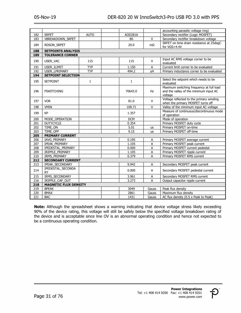
05-Nov-19 DER-820 20 W InnoSwitch3-Pro USB PD 3.0 with PPS
Page 31 of 76
Power Integrations Tel: +1 408 414 9200 Fax: +1 408 414 9201
www.power.com
accounting parasitic voltage ring)
182 SRFET AUTO
AOD2816
Secondary rectifier (Logic MOSFET)
183 VBREAKDOWN_SRFET
80 V Secondary rectifier breakdown voltage
184 RDSON_SRFET
29.0 mΩ SRFET on time drain resistance at 25degC for VGS=4.4V
188 SETPOINTS ANALYSIS
189 TOLERANCE CORNER
190 USER_VAC 115
115 V Input AC RMS voltage corner to be evaluated
191 USER_ILIMIT TYP
1.150 A Current limit corner to be evaluated
192 USER_LPRIMARY TYP
494.2 uH Primary inductance corner to be evaluated
194 SETPOINT SELECTION
195 SETPOINT 1
1
Select the setpoint which needs to be evaluated
196 FSWITCHING
70643.0 Hz Maximum switching frequency at full load and the valley of the minimum input AC voltage
197 VOR
81.0 V Voltage reflected to the primary winding when the primary MOSFET turns off
198 VMIN
109.71 V Valley of the minimum input AC voltage
199 KP
1.357
Measure of continuous/discontinuous mode of operation
200 MODE_OPERATION
DCM
Mode of operation
201 DUTYCYCLE
0.354
Primary MOSFET duty cycle
202 TIME_ON
5.01 us Primary MOSFET on-time
203 TIME_OFF
9.15 us Primary MOSFET off-time
205 PRIMARY CURRENT
206 IAVG_PRIMARY
0.195 A Primary MOSFET average current
207 IPEAK_PRIMARY
1.105 A Primary MOSFET peak current
208 IPEDESTAL_PRIMARY
0.000 A Primary MOSFET current pedestal
209 IRIPPLE_PRIMARY
1.105 A Primary MOSFET ripple current
210 IRMS_PRIMARY
0.379 A Primary MOSFET RMS current
212 SECONDARY CURRENT
213 IPEAK_SECONDARY
9.942 A Secondary MOSFET peak current
214 IPEDESTAL_SECONDARY
0.000 A Secondary MOSFET pedestal current
215 IRMS_SECONDARY
3.961 A Secondary MOSFET RMS current
216 IRIPPLE_CAP_OUT
3.273 A Output capacitor ripple current
218 MAGNETIC FLUX DENSITY
219 BPEAK
3049 Gauss Peak flux density
220 BMAX
2861 Gauss Maximum flux density
221 BAC
1431 Gauss AC flux density (0.5 x Peak to Peak)
Note: Although the spreadsheet shows a warning indicating that device voltage stress likely exceeding
90% of the device rating, this voltage will still be safely below the specified voltage breakdown rating of the device and is acceptable since line OV is an abnormal operating condition and hence not expected to
be a continuous operating condition.
DER-820 20 W InnoSwitch3-Pro USB PD 3.0 with PPS 05-Nov-19
Page 32 of 76
Power Integrations, Inc. Tel: +1 408 414 9200 Fax: +1 408 414 9201 www.power.com
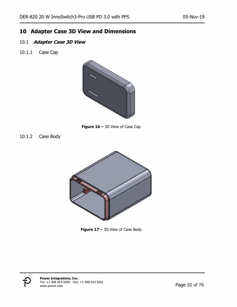
Adapter Case 3D View and Dimensions 10
Adapter Case 3D View 10.1
Case Cap 10.1.1
Figure 16 – 3D View of Case Cap.
Case Body 10.1.2
Figure 17 – 3D View of Case Body.

05-Nov-19 DER-820 20 W InnoSwitch3-Pro USB PD 3.0 with PPS
Page 33 of 76
Power Integrations Tel: +1 408 414 9200 Fax: +1 408 414 9201
www.power.com
Entire Case 10.1.3
Figure 18 – 3D View of Entire Case.

DER-820 20 W InnoSwitch3-Pro USB PD 3.0 with PPS 05-Nov-19
Page 34 of 76
Power Integrations, Inc. Tel: +1 408 414 9200 Fax: +1 408 414 9201 www.power.com
Adapter Case Dimensions 10.2
Case Cap 10.2.1
Figure 19 – Dimensions of Case Cap.

05-Nov-19 DER-820 20 W InnoSwitch3-Pro USB PD 3.0 with PPS
Page 35 of 76
Power Integrations Tel: +1 408 414 9200 Fax: +1 408 414 9201
www.power.com
Case Body 10.2.2
Figure 20 – Dimensions of Case Body.
DER-820 20 W InnoSwitch3-Pro USB PD 3.0 with PPS 05-Nov-19
Page 36 of 76
Power Integrations, Inc. Tel: +1 408 414 9200 Fax: +1 408 414 9201 www.power.com
Performance Data 11
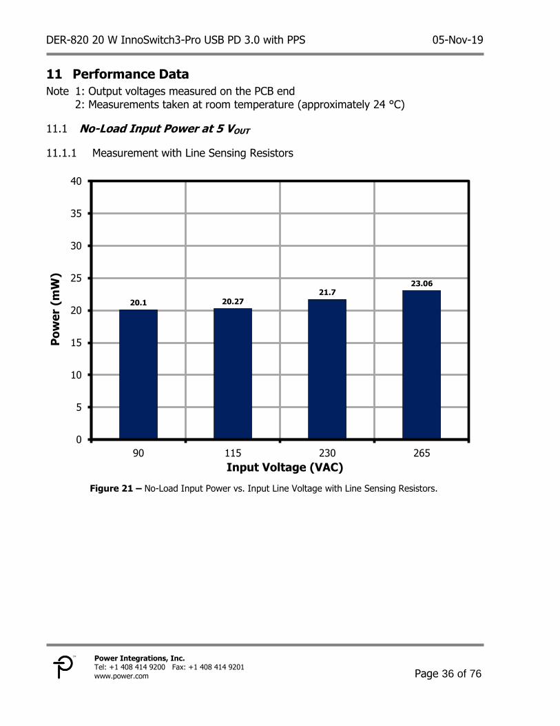
Note 1: Output voltages measured on the PCB end 2: Measurements taken at room temperature (approximately 24 °C)
No-Load Input Power at 5 VOUT 11.1
Measurement with Line Sensing Resistors 11.1.1
Figure 21 – No-Load Input Power vs. Input Line Voltage with Line Sensing Resistors.
20.1 20.2721.7
23.06
0
5
10
15
20
25
30
35
40
90 115 230 265
Po
we
r (m
W)
Input Voltage (VAC)

05-Nov-19 DER-820 20 W InnoSwitch3-Pro USB PD 3.0 with PPS
Page 37 of 76
Power Integrations Tel: +1 408 414 9200 Fax: +1 408 414 9201
www.power.com
Measurement without Line Sensing Resistors 11.1.2
Figure 22 – No-Load Input Power vs. Input Line Voltage without Line Sensing Resistors.
19.95 20.0721.06
22.09
0
5
10
15
20
25
30
35
40
90 115 230 265
Po
we
r (m
W)
Input Voltage (VAC)

DER-820 20 W InnoSwitch3-Pro USB PD 3.0 with PPS 05-Nov-19
Page 38 of 76
Power Integrations, Inc. Tel: +1 408 414 9200 Fax: +1 408 414 9201 www.power.com
Average and 10% Load Efficiency 11.2
Efficiency Requirements 11.2.1
Test Average Average 10% Load
Effective 2016 Jan-16 Jan-16
VOUT
(V)
Model
(V)
Power
(W)
New
EISA2007
CoC v5
Tier 2
CoC v5
Tier 2
5 <6 15 81.4% 81.8% 72.5%
9 >6 20 85.4% 85.9% 75.9%
Efficiency Performance Summary 11.2.2
On Board 11.2.2.1
VOUT
(V)
Power
(W)
Average Efficiency (%) 10% Load Efficiency (%)
115 VAC 230 VAC 115 VAC 230 VAC
5 15 87.91 87.76 85.81 82.56
9 20 87.75 88.06 82.31 79.99
End of Cable 11.2.2.2
VOUT (V)
Power (W)
Average Efficiency (%) 10% Load Efficiency (%)
115 VAC 230 VAC 115 VAC 230 VAC
5 15 83.53 83.36 84.90 81.63
9 20 86.32 86.46 82.22 79.68
Average and 10% Load Efficiency at 115 VAC 11.2.3
Output: 5 V / 3 A (On Board) 11.2.3.1
Load (%)
Efficiency (%)
Average Efficiency (%) [100% - 25% Load]
100 87.71
87.91 75 87.98
50 88.19
25 87.76
10 85.81
05-Nov-19 DER-820 20 W InnoSwitch3-Pro USB PD 3.0 with PPS
Page 39 of 76
Power Integrations Tel: +1 408 414 9200 Fax: +1 408 414 9201
www.power.com
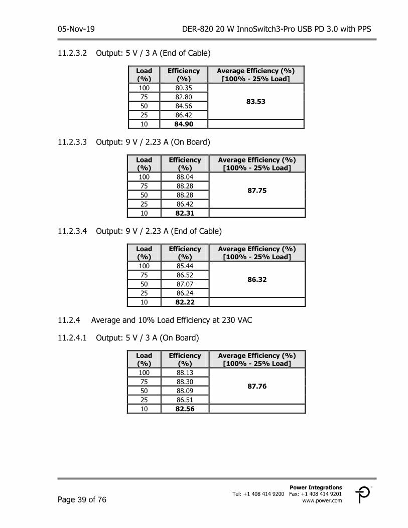
Output: 5 V / 3 A (End of Cable) 11.2.3.2
Load
(%)
Efficiency
(%)
Average Efficiency (%)
[100% - 25% Load]
100 80.35
83.53 75 82.80
50 84.56
25 86.42
10 84.90
Output: 9 V / 2.23 A (On Board) 11.2.3.3
Load (%)
Efficiency (%)
Average Efficiency (%) [100% - 25% Load]
100 88.04
87.75 75 88.28
50 88.28
25 86.42
10 82.31
Output: 9 V / 2.23 A (End of Cable) 11.2.3.4
Load (%)
Efficiency (%)
Average Efficiency (%) [100% - 25% Load]
100 85.44
86.32 75 86.52
50 87.07
25 86.24
10 82.22
Average and 10% Load Efficiency at 230 VAC 11.2.4
Output: 5 V / 3 A (On Board) 11.2.4.1
Load (%)
Efficiency (%)
Average Efficiency (%) [100% - 25% Load]
100 88.13
87.76 75 88.30
50 88.09
25 86.51
10 82.56

DER-820 20 W InnoSwitch3-Pro USB PD 3.0 with PPS 05-Nov-19
Page 40 of 76
Power Integrations, Inc. Tel: +1 408 414 9200 Fax: +1 408 414 9201 www.power.com
Output: 5 V / 3 A (End of Cable) 11.2.4.2
Load
(%)
Efficiency
(%)
Average Efficiency (%)
[100% - 25% Load]
100 80.90
83.36 75 83.11
50 84.54
25 84.91
10 81.63
Output: 9 V / 2.23 A (On Board) 11.2.4.3
Load (%)
Efficiency (%)
Average Efficiency (%) [100% - 25% Load]
100 89.14
88.06 75 88.97
50 88.49
25 85.62
10 79.99
Output: 9 V / 2.23 A (End of Cable) 11.2.4.4
Load (%)
Efficiency (%)
Average Efficiency (%) [100% - 25% Load]
100 86.37
86.46 75 87.09
50 87.14
25 85.23
10 79.68

05-Nov-19 DER-820 20 W InnoSwitch3-Pro USB PD 3.0 with PPS
Page 41 of 76
Power Integrations Tel: +1 408 414 9200 Fax: +1 408 414 9201
www.power.com
Efficiency Across Load 11.3
Output: 5 V / 3 A (On Board) 11.3.1
Figure 23 – Efficiency vs. Load for 5 V Output, Room Temperature.
50
55
60
65
70
75
80
85
90
95
100
10 20 30 40 50 60 70 80 90 100
Eff
icie
ncy (
%)
Load (%)
90 VAC
115 VAC
230 VAC
265 VAC

DER-820 20 W InnoSwitch3-Pro USB PD 3.0 with PPS 05-Nov-19
Page 42 of 76
Power Integrations, Inc. Tel: +1 408 414 9200 Fax: +1 408 414 9201 www.power.com
Output: 5 V / 3 A (End of Cable) 11.3.2
Figure 24 – Efficiency vs. Load for 5 V Output, Room Temperature.
50
55
60
65
70
75
80
85
90
95
100
10 20 30 40 50 60 70 80 90 100
Eff
icie
ncy (
%)
Load (%)
90 VAC
115 VAC
230 VAC
265 VAC

05-Nov-19 DER-820 20 W InnoSwitch3-Pro USB PD 3.0 with PPS
Page 43 of 76
Power Integrations Tel: +1 408 414 9200 Fax: +1 408 414 9201
www.power.com
Output: 9 V / 2.23 A (On Board) 11.3.3
Figure 25 – Efficiency vs. Load for 9 V Output, Room Temperature.
50
55
60
65
70
75
80
85
90
95
100
10 20 30 40 50 60 70 80 90 100
Eff
icie
ncy (
%)
Load (%)
90 VAC
115 VAC
230 VAC
265 VAC

DER-820 20 W InnoSwitch3-Pro USB PD 3.0 with PPS 05-Nov-19
Page 44 of 76
Power Integrations, Inc. Tel: +1 408 414 9200 Fax: +1 408 414 9201 www.power.com
Output: 9 V / 2.23 A (End of Cable) 11.3.4
Figure 26 – Efficiency vs. Load for 9 V Output, Room Temperature.
50
55
60
65
70
75
80
85
90
95
100
10 20 30 40 50 60 70 80 90 100
Eff
icie
ncy (
%)
Load (%)
90 VAC
115 VAC
230 VAC
265 VAC

05-Nov-19 DER-820 20 W InnoSwitch3-Pro USB PD 3.0 with PPS
Page 45 of 76
Power Integrations Tel: +1 408 414 9200 Fax: +1 408 414 9201
www.power.com
Efficiency Across Line (On Board) 11.4
Figure 27 – Full Load Efficiency vs. Input Line for 3.3 V, 5 V, 9 V, and 11 V Output, Room Temperature.
50
55
60
65
70
75
80
85
90
95
100
80 100 120 140 160 180 200 220 240 260 280
Eff
icie
ncy (
%)
Input Voltage (VAC)
3.3 V / 3 A
5 V / 3 A
9 V / 2.23 A
11 V/ 1.81 A
DER-820 20 W InnoSwitch3-Pro USB PD 3.0 with PPS 05-Nov-19
Page 46 of 76
Power Integrations, Inc. Tel: +1 408 414 9200 Fax: +1 408 414 9201 www.power.com
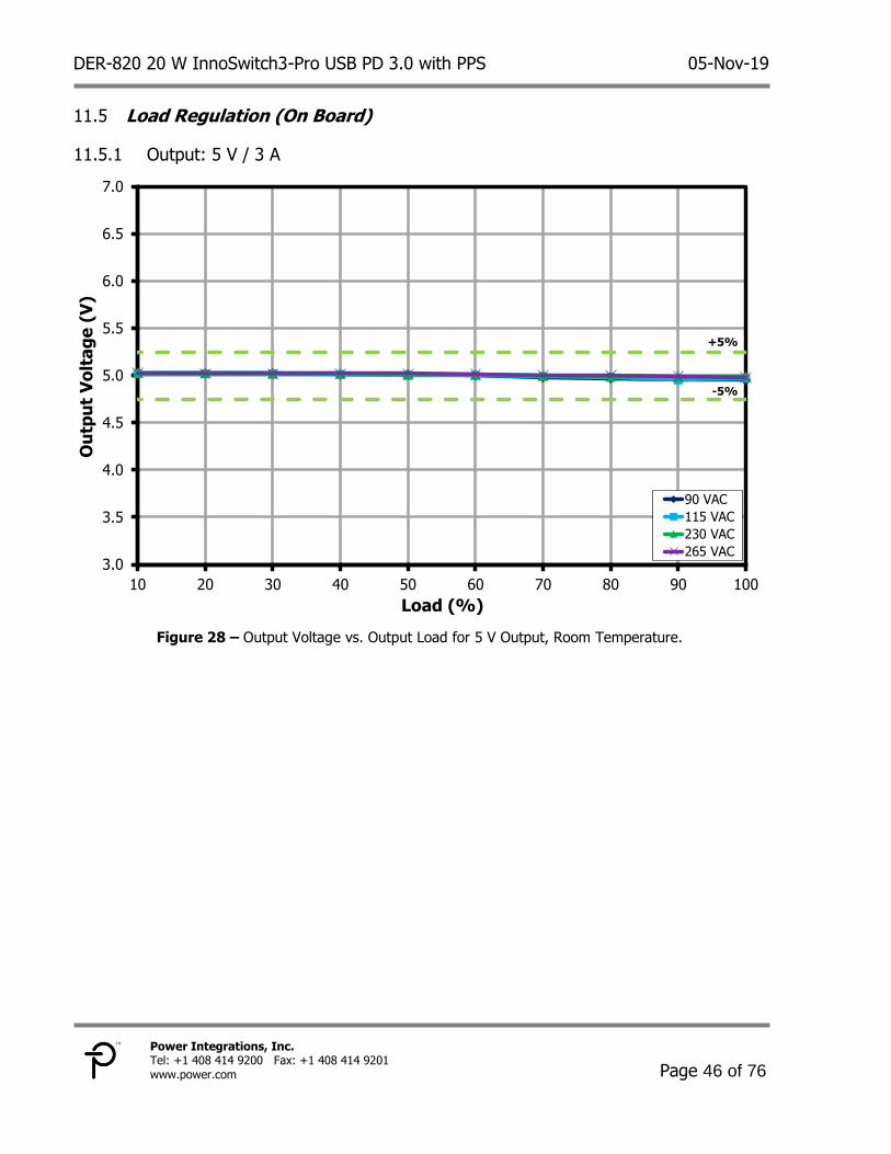
Load Regulation (On Board) 11.5
Output: 5 V / 3 A 11.5.1
Figure 28 – Output Voltage vs. Output Load for 5 V Output, Room Temperature.
+5%
-5%
3.0
3.5
4.0
4.5
5.0
5.5
6.0
6.5
7.0
10 20 30 40 50 60 70 80 90 100
Ou
tpu
t V
olt
ag
e (
V)
Load (%)
90 VAC
115 VAC
230 VAC
265 VAC
05-Nov-19 DER-820 20 W InnoSwitch3-Pro USB PD 3.0 with PPS
Page 47 of 76
Power Integrations Tel: +1 408 414 9200 Fax: +1 408 414 9201
www.power.com
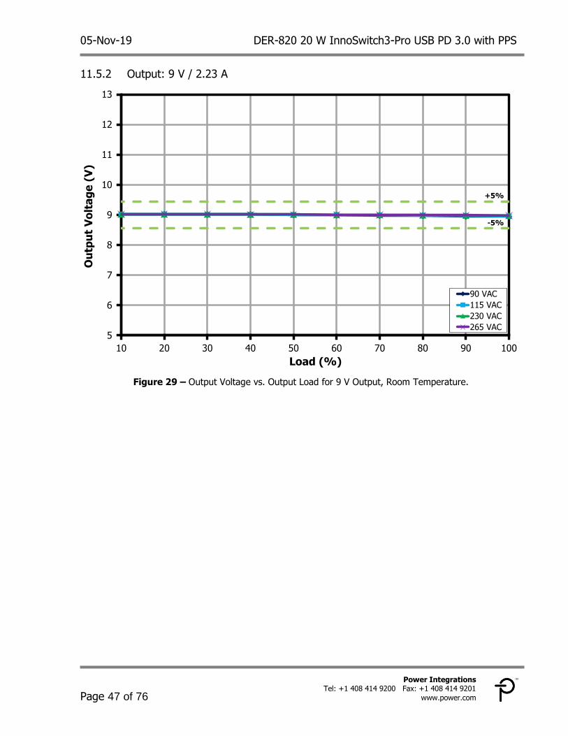
Output: 9 V / 2.23 A 11.5.2
Figure 29 – Output Voltage vs. Output Load for 9 V Output, Room Temperature.
+5%
-5%
5
6
7
8
9
10
11
12
13
10 20 30 40 50 60 70 80 90 100
Ou
tpu
t V
olt
ag
e (
V)
Load (%)
90 VAC
115 VAC
230 VAC
265 VAC

DER-820 20 W InnoSwitch3-Pro USB PD 3.0 with PPS 05-Nov-19
Page 48 of 76
Power Integrations, Inc. Tel: +1 408 414 9200 Fax: +1 408 414 9201 www.power.com
Line Regulation (On Board) 11.6
Output: 5 V / 3 A 11.6.1
Figure 30 – Output Voltage vs. Input Line Voltage for 5 V Output, Room Temperature.
3.0
3.5
4.0
4.5
5.0
5.5
6.0
6.5
7.0
80 100 120 140 160 180 200 220 240 260 280
Ou
tpu
t V
olt
ag
e (
V)
Input Voltage (VAC)
100% Load
50% Load
05-Nov-19 DER-820 20 W InnoSwitch3-Pro USB PD 3.0 with PPS
Page 49 of 76
Power Integrations Tel: +1 408 414 9200 Fax: +1 408 414 9201
www.power.com
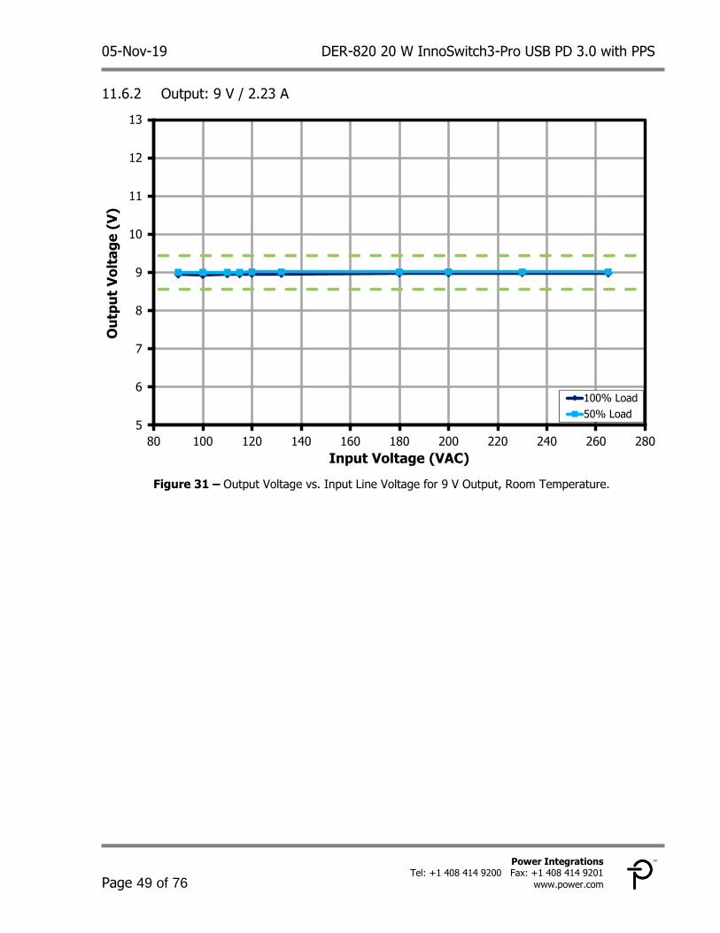
Output: 9 V / 2.23 A 11.6.2
Figure 31 – Output Voltage vs. Input Line Voltage for 9 V Output, Room Temperature.
5
6
7
8
9
10
11
12
13
80 100 120 140 160 180 200 220 240 260 280
Ou
tpu
t V
olt
ag
e (
V)
Input Voltage (VAC)
100% Load
50% Load

DER-820 20 W InnoSwitch3-Pro USB PD 3.0 with PPS 05-Nov-19
Page 50 of 76
Power Integrations, Inc. Tel: +1 408 414 9200 Fax: +1 408 414 9201 www.power.com
Thermal Performance 12
Open Case Measurement 12.1
Output: 5 V / 3 A (90 VAC) at 26.9 ºC Ambient 12.1.1
Figure 32 – Top Side Thermal Image.
El1: Transformer T1 = 70.8 ºC. El2: Thermistor RT2 = 79.9 ºC.
Figure 33 – Bottom Side Thermal Image.
Bx1: InnoSwitch3-Pro = 77.5 ºC. Bx2: PCB, SR FET Q2 = 72.7 ºC.
Bx3: Bridge Rectifier BR1 = 69.7 ºC.
Output: 5 V / 3 A (265 VAC) at 25.8 ºC Ambient 12.1.2
Figure 34 – Top Side Thermal Image. El1: Transformer T1 = 73.5 ºC.
El2: Thermistor RT2 = 54.2 ºC.
Figure 35 – Bottom Side Thermal Image. Bx1: InnoSwitch3-Pro = 74.9 ºC.
Bx2: PCB, SR FET Q2 = 74.1 ºC.
Bx3: Bridge Rectifier BR1 = 48.6 ºC.

05-Nov-19 DER-820 20 W InnoSwitch3-Pro USB PD 3.0 with PPS
Page 51 of 76
Power Integrations Tel: +1 408 414 9200 Fax: +1 408 414 9201
www.power.com
Output: 9 V / 2.23 A (90 VAC) at 27.7 ºC Ambient 12.1.3
Figure 36 – Top Side Thermal Image.
El1: Transformer T1 = 78.7 ºC. El2: Thermistor RT2 = 93.5 ºC.
Figure 37 – Bottom Side Thermal Image.
Bx1: InnoSwitch3-Pro = 92.4 ºC. Bx2: PCB, SR FET Q2 = 79.8 ºC.
Bx3: Bridge Rectifier BR1 = 84.7 ºC.
Output: 9 V / 2.23 A (265 VAC) at 26.2 ºC Ambient 12.1.4
Figure 38 – Top Side Thermal Image. El1: Transformer T1 = 78.0 ºC.
El2: Thermistor RT2 = 62.2 ºC.
Figure 39 – Bottom Side Thermal Image. Bx1: InnoSwitch3-Pro = 82.8ºC.
Bx2: PCB, SR FET Q2 = 77.3 ºC.
Bx3: Bridge Rectifier BR1 = 54.1 ºC.
DER-820 20 W InnoSwitch3-Pro USB PD 3.0 with PPS 05-Nov-19
Page 52 of 76
Power Integrations, Inc. Tel: +1 408 414 9200 Fax: +1 408 414 9201 www.power.com
Adapter Case Enclosure Measurement 12.2
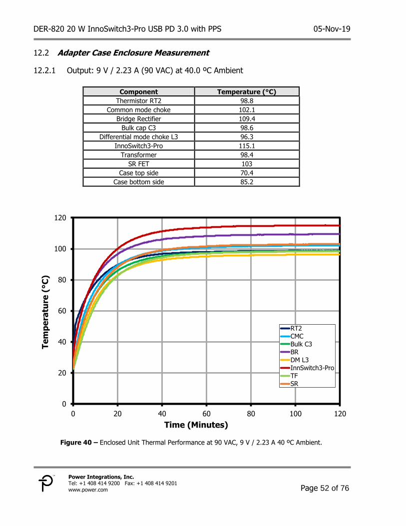
Output: 9 V / 2.23 A (90 VAC) at 40.0 ºC Ambient 12.2.1
Component Temperature (°C)
Thermistor RT2 98.8
Common mode choke 102.1
Bridge Rectifier 109.4
Bulk cap C3 98.6
Differential mode choke L3 96.3
InnoSwitch3-Pro 115.1
Transformer 98.4
SR FET 103
Case top side 70.4
Case bottom side 85.2
Figure 40 – Enclosed Unit Thermal Performance at 90 VAC, 9 V / 2.23 A 40 ºC Ambient.
0
20
40
60
80
100
120
0 20 40 60 80 100 120
Te
mp
era
ture
(°C
)
Time (Minutes)
RT2
CMC
Bulk C3
BR
DM L3
InnSwitch3-Pro
TF
SR
05-Nov-19 DER-820 20 W InnoSwitch3-Pro USB PD 3.0 with PPS
Page 53 of 76
Power Integrations Tel: +1 408 414 9200 Fax: +1 408 414 9201
www.power.com
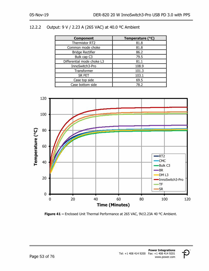
Output: 9 V / 2.23 A (265 VAC) at 40.0 ºC Ambient 12.2.2
Component Temperature (°C)
Thermistor RT2 81.8
Common mode choke 81.8
Bridge Rectifier 86.2
Bulk cap C3 79.5
Differential mode choke L3 81.1
InnoSwitch3-Pro 108.9
Transformer 101.3
SR FET 103.1
Case top side 69.5
Case bottom side 78.2
Figure 41 – Enclosed Unit Thermal Performance at 265 VAC, 9V/2.23A 40 ºC Ambient.
0
20
40
60
80
100
120
0 20 40 60 80 100 120
Te
mp
era
ture
(°C
)
Time (Minutes)
RT2
CMC
Bulk C3
BR
DM L3
InnoSwitch3-Pro
TF
SR

DER-820 20 W InnoSwitch3-Pro USB PD 3.0 with PPS 05-Nov-19
Page 54 of 76
Power Integrations, Inc. Tel: +1 408 414 9200 Fax: +1 408 414 9201 www.power.com
Waveforms 13
Output Voltage and Current at Start-up (On the Board) 13.1
Figure 42 – Output Voltage and Current Waveforms.
90 VAC, 5.0 V, 3 A Load (5.18 VMAX).
CH3: ILOAD, 1 A / div. CH4: VOUT, 1 V / div.
Time: 500 ms / div. (100 s / div. Zoom).
Figure 43 – Drain Voltage and Current Waveforms.
265 VAC, 5.0 V, 3 A Load (5.21 VMAX).
CH3: ILOAD, 1 A / div. CH4: VOUT, 1 V / div.
Time: 500 ms / div. (100 s / div. Zoom).
Load Transient Response 13.2
Note: Output voltages captured at the end of 100 mΩ cable
Output: 5 V / 3 A 13.2.1
Figure 44 – Transient Response.
90VAC, 5.0 V, 0 – 0.75 A Load Step.
VMIN: 4.864 V, VMAX: 5.101 V.
CH1: VOUT, 0.2 V / div.
CH3: ILOAD, 1 A / div. Time: 5 ms / div. (1.5 ms / div. Zoom).
Figure 45 – Transient Response.
265VAC, 5.0 V, 0 – 0.75 A Load Step.
VMIN : 4.890 V, VMAX: 5.107 V.
CH1: VOUT, 0.2 V / div.
CH3: ILOAD, 1 A / div. Time: 5 ms / div. (1.5 ms / div. Zoom).
05-Nov-19 DER-820 20 W InnoSwitch3-Pro USB PD 3.0 with PPS
Page 55 of 76
Power Integrations Tel: +1 408 414 9200 Fax: +1 408 414 9201
www.power.com
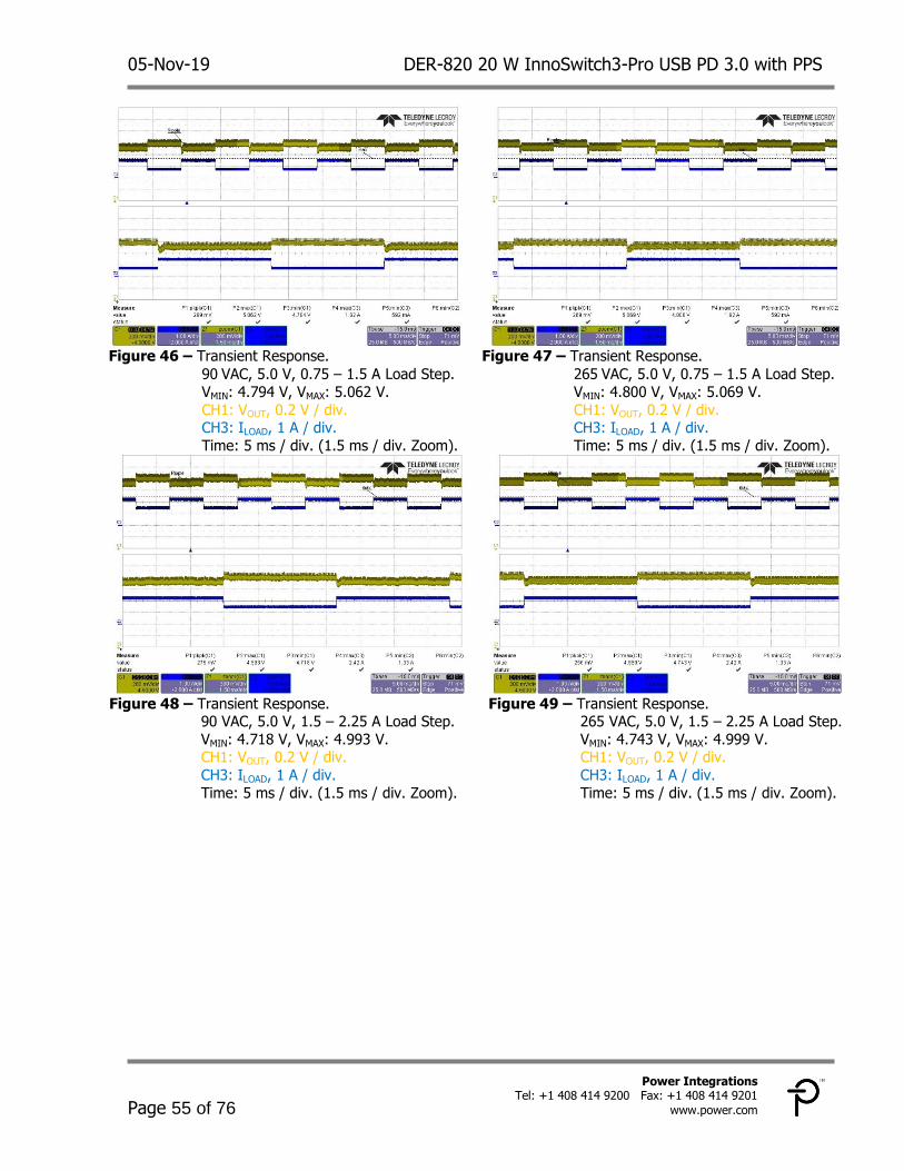
Figure 46 – Transient Response.
90VAC, 5.0 V, 0.75 – 1.5 A Load Step.
VMIN: 4.794 V, VMAX: 5.062 V.
CH1: VOUT, 0.2 V / div. CH3: ILOAD, 1 A / div.
Time: 5 ms / div. (1.5 ms / div. Zoom).
Figure 47 – Transient Response.
265VAC, 5.0 V, 0.75 – 1.5 A Load Step.
VMIN: 4.800 V, VMAX: 5.069 V.
CH1: VOUT, 0.2 V / div. CH3: ILOAD, 1 A / div.
Time: 5 ms / div. (1.5 ms / div. Zoom).
Figure 48 – Transient Response.
90 VAC, 5.0 V, 1.5 – 2.25 A Load Step.
VMIN: 4.718 V, VMAX: 4.993 V. CH1: VOUT, 0.2 V / div.
CH3: ILOAD, 1 A / div.
Time: 5 ms / div. (1.5 ms / div. Zoom).
Figure 49 – Transient Response. 265 VAC, 5.0 V, 1.5 – 2.25 A Load Step.
VMIN: 4.743 V, VMAX: 4.999 V. CH1: VOUT, 0.2 V / div.
CH3: ILOAD, 1 A / div.
Time: 5 ms / div. (1.5 ms / div. Zoom).

DER-820 20 W InnoSwitch3-Pro USB PD 3.0 with PPS 05-Nov-19
Page 56 of 76
Power Integrations, Inc. Tel: +1 408 414 9200 Fax: +1 408 414 9201 www.power.com
Figure 50 – Transient Response.
90 VAC, 5.0 V, 2.25 – 3 A Load Step. VMIN: 4.626 V, VMAX: 4.908 V.
CH1: VOUT, 0.2 V / div. CH3: ILOAD, 1 A / div.
Time: 5 ms / div. (1.5 ms / div. Zoom).
Figure 51 – Transient Response.
265 VAC, 5.0 V, 2.25 – 3 A Load Step. VMIN: 4.652 V, VMAX: 4.921 V.
CH1: VOUT, 0.2 V / div. CH3: ILOAD, 1 A / div.
Time: 5 ms / div. (1.5 ms / div. Zoom).
Output: 9 V / 2.23 A 13.2.2
Figure 52 – Transient Response.
90VAC, 9.0 V, 0 – 0.55 A Load Step.
VMIN: 8.841 V, VMAX: 9.103 V.
CH1: VOUT, 0.2 V / div. CH3: ILOAD, 1 A / div.
Time: 5 ms / div. (1.5 ms / div. Zoom).
Figure 53 – Transient Response.
265VAC, 9.0 V, 0 – 0.55 A Load Step.
VMIN 8.847 V, VMAX: 9.103 V.
CH1: VOUT, 0.2 V / div. CH3: ILOAD, 1 A / div.
Time: 5 ms / div. (1.5 ms / div. Zoom).

05-Nov-19 DER-820 20 W InnoSwitch3-Pro USB PD 3.0 with PPS
Page 57 of 76
Power Integrations Tel: +1 408 414 9200 Fax: +1 408 414 9201
www.power.com
Figure 54 – Transient Response.
90VAC, 9.0 V, 0.55 – 1.1 A Load Step.
VMIN: 8.815 V, VMAX: 9.090 V. CH1: VOUT, 0.2 V / div.
CH3: ILOAD, 1 A / div. Time: 5 ms / div. (1.5 ms / div. Zoom).
Figure 55 – Transient Response.
265VAC, 9.0 V, 0.55 – 1.1 A Load Step.
VMIN: 8.828 V, VMAX: 9.097 V. CH1: VOUT, 0.2 V / div.
CH3: ILOAD, 1 A / div. Time: 5 ms / div. (1.5 ms / div. Zoom).
Figure 56 – Transient Response.
90 VAC, 9.0 V, 1.1 – 1.65 A Load Step. VMIN: 8.764 V, VMAX: 9.039 V.
CH1: VOUT, 0.2 V / div. CH3: ILOAD, 1 A / div.
Time: 5 ms / div. (1.5 ms / div. Zoom).
Figure 57 – Transient Response.
265 VAC, 9.0 V, 1.1 – 1.65 A Load Step. VMIN: 8.783 V, VMAX: 9.058 V.
CH1: VOUT, 0.2 V / div. CH3: ILOAD, 1 A / div.
Time: 5 ms / div. (1.5 ms / div. Zoom).

DER-820 20 W InnoSwitch3-Pro USB PD 3.0 with PPS 05-Nov-19
Page 58 of 76
Power Integrations, Inc. Tel: +1 408 414 9200 Fax: +1 408 414 9201 www.power.com
Figure 58 – Transient Response.
90 VAC, 9.0 V, 1.65 – 2.23 A Load Step. VMIN: 8.687 V, VMAX: 8.994 V. CH1: VOUT, 0.2 V / div. CH3: ILOAD, 1 A / div.
Time: 5 ms / div. (1.5 ms / div. Zoom).
Figure 59 – Transient Response.
265 VAC, 9.0 V, 1.65 – 2.23 A Load Step. VMIN: 8.726 V, VMAX: 9.007 V.
CH1: VOUT, 0.2 V / div. CH3: ILOAD, 1 A / div.
Time: 5 ms / div. (1.5 ms / div. Zoom).
Switching Waveforms 13.3
Primary Drain Voltage and Current 13.3.1
Figure 60 – Drain Voltage and Current Waveforms. 90 VAC, 5.0 V, 3 A Load (225 VMAX).
CH2: VDRAIN, 100 V / div.
CH3: IDRAIN, 1 A / div.
Time: 10 s / div.
Figure 61 – Drain Voltage and Current Waveforms. 265 VAC, 5.0 V, 3 A Load (495 VMAX).
CH2: VDRAIN, 200 V / div.
CH3: IDRAIN, 1 A / div.
Time: 10 s / div.

05-Nov-19 DER-820 20 W InnoSwitch3-Pro USB PD 3.0 with PPS
Page 59 of 76
Power Integrations Tel: +1 408 414 9200 Fax: +1 408 414 9201
www.power.com
Figure 62 – Drain Voltage and Current Waveforms.
90 VAC, 9.0 V, 2.23 A Load (235 VMAX).
CH2: VDRAIN, 100 V / div. CH3: IDRAIN, 1 A / div.
Time: 10 s / div.
Figure 63 – Drain Voltage and Current Waveforms.
265 VAC, 9 V, 2.23 A Load (521 VMAX).
CH2: VDRAIN, 200 V / div. CH3: IDRAIN, 1 A / div.
Time: 10 s / div.
Primary Drain Voltage and Current at Start-up 13.3.2
Figure 64 – Drain Voltage and Current Waveforms. 90 VAC, 5.0 V, 3 A Load (238 VMAX).
CH2: VDRAIN, 100 V / div. CH3: IDRAIN, 1 A / div.
Time: 50 ms / div. (500 s / div. Zoom).
Figure 65 – Drain Voltage and Current Waveforms. 265 VAC, 5.0 V, 3 A Load (495 VMAX).
CH2: VDRAIN, 200 V / div. CH3: IDRAIN, 1 A / div.
Time: 50 ms / div. (500 s / div. Zoom).
DER-820 20 W InnoSwitch3-Pro USB PD 3.0 with PPS 05-Nov-19
Page 60 of 76
Power Integrations, Inc. Tel: +1 408 414 9200 Fax: +1 408 414 9201 www.power.com
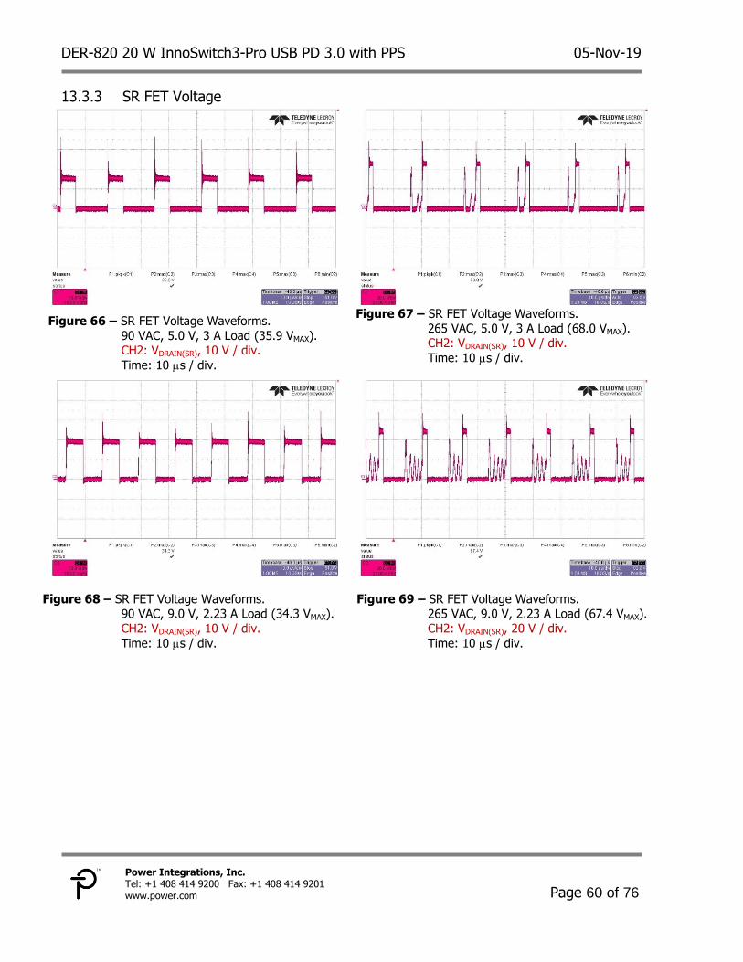
SR FET Voltage 13.3.3
Figure 66 – SR FET Voltage Waveforms.
90 VAC, 5.0 V, 3 A Load (35.9 VMAX). CH2: VDRAIN(SR), 10 V / div.
Time: 10 s / div.
Figure 67 – SR FET Voltage Waveforms.
265 VAC, 5.0 V, 3 A Load (68.0 VMAX). CH2: VDRAIN(SR), 10 V / div.
Time: 10 s / div.
Figure 68 – SR FET Voltage Waveforms.
90 VAC, 9.0 V, 2.23 A Load (34.3 VMAX). CH2: VDRAIN(SR), 10 V / div.
Time: 10 s / div.
Figure 69 – SR FET Voltage Waveforms.
265 VAC, 9.0 V, 2.23 A Load (67.4 VMAX). CH2: VDRAIN(SR), 20 V / div.
Time: 10 s / div.

05-Nov-19 DER-820 20 W InnoSwitch3-Pro USB PD 3.0 with PPS
Page 61 of 76
Power Integrations Tel: +1 408 414 9200 Fax: +1 408 414 9201
www.power.com
Output Ripple Measurements 14
Ripple Measurement Technique 14.1
For DC output ripple measurements, a modified oscilloscope test probe must be utilized in order to reduce spurious signals due to pick-up. Details of the probe modification are provided in the Figures below. The 4987BA probe adapter is affixed with two capacitors tied in parallel across the probe
tip. The capacitors include one (1) 0.1 F/50 V ceramic type and one (1) 47 F/50 V
aluminum electrolytic. The aluminum electrolytic type capacitor is polarized, so proper polarity across DC outputs must be maintained (see below).
Figure 70 – Oscilloscope Probe Prepared for Ripple Measurement. (End Cap and Ground Lead Removed)
Figure 71 – Oscilloscope Probe with Probe Master (www.probemaster.com) 4987A BNC Adapter.
(Modified with wires for ripple measurement, and two parallel decoupling capacitors added)
Probe Ground
Probe Tip
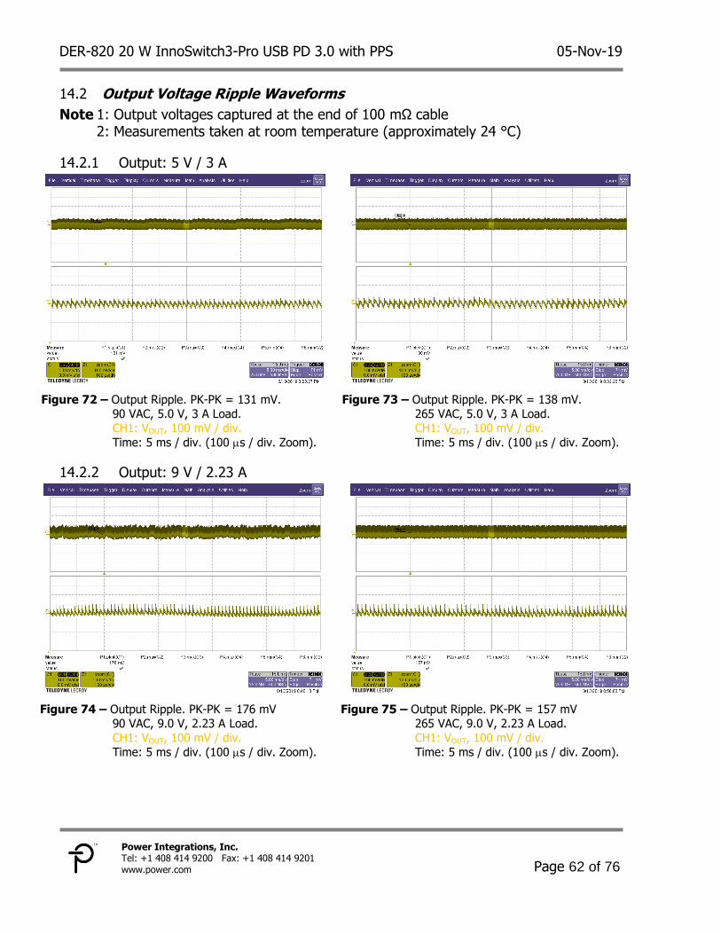
DER-820 20 W InnoSwitch3-Pro USB PD 3.0 with PPS 05-Nov-19
Page 62 of 76
Power Integrations, Inc. Tel: +1 408 414 9200 Fax: +1 408 414 9201 www.power.com
Output Voltage Ripple Waveforms 14.2
Note 1: Output voltages captured at the end of 100 mΩ cable 2: Measurements taken at room temperature (approximately 24 °C)
Output: 5 V / 3 A 14.2.1
Figure 72 – Output Ripple. PK-PK = 131 mV.
90 VAC, 5.0 V, 3 A Load. CH1: VOUT, 100 mV / div.
Time: 5 ms / div. (100 s / div. Zoom).
Figure 73 – Output Ripple. PK-PK = 138 mV.
265 VAC, 5.0 V, 3 A Load. CH1: VOUT, 100 mV / div.
Time: 5 ms / div. (100 s / div. Zoom).
Output: 9 V / 2.23 A 14.2.2
Figure 74 – Output Ripple. PK-PK = 176 mV
90 VAC, 9.0 V, 2.23 A Load.
CH1: VOUT, 100 mV / div.
Time: 5 ms / div. (100 s / div. Zoom).
Figure 75 – Output Ripple. PK-PK = 157 mV
265 VAC, 9.0 V, 2.23 A Load.
CH1: VOUT, 100 mV / div.
Time: 5 ms / div. (100 s / div. Zoom).
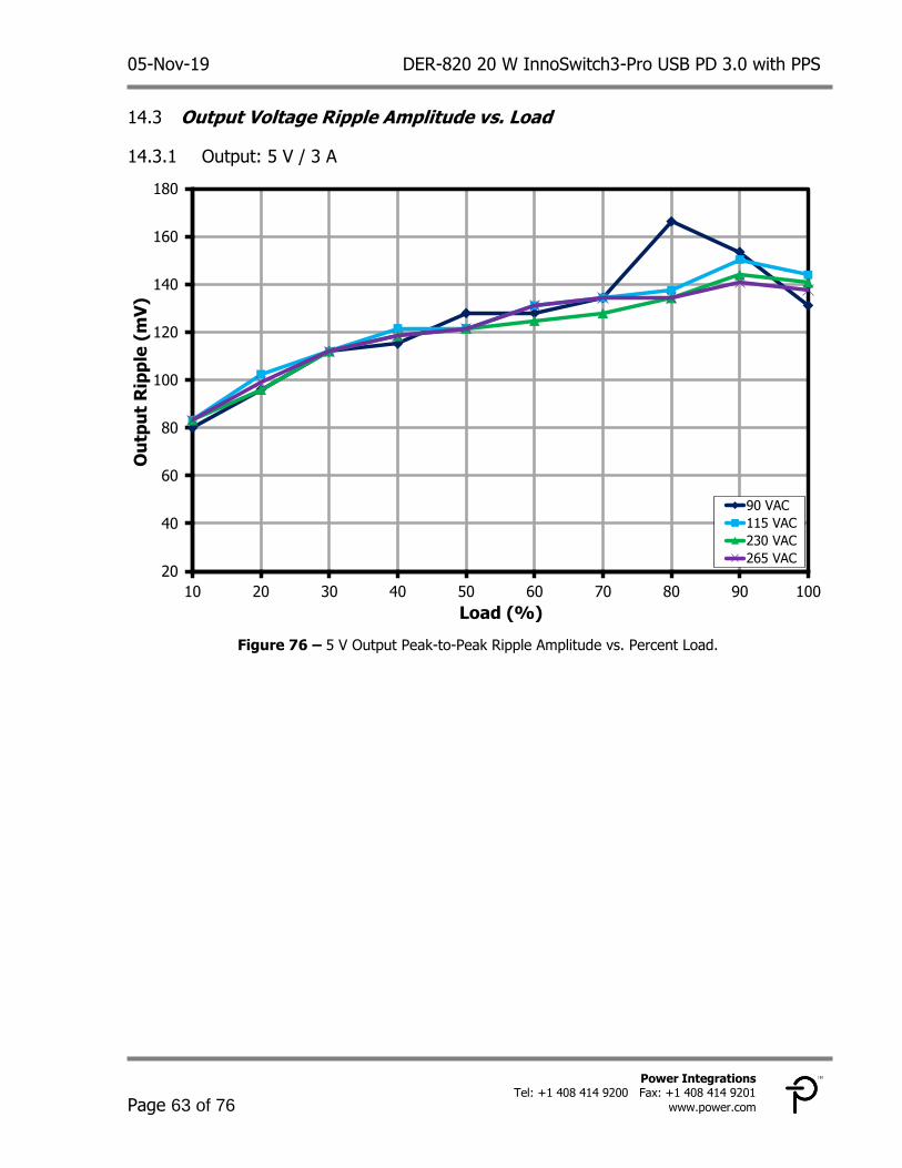
05-Nov-19 DER-820 20 W InnoSwitch3-Pro USB PD 3.0 with PPS
Page 63 of 76
Power Integrations Tel: +1 408 414 9200 Fax: +1 408 414 9201
www.power.com
Output Voltage Ripple Amplitude vs. Load 14.3
Output: 5 V / 3 A 14.3.1
Figure 76 – 5 V Output Peak-to-Peak Ripple Amplitude vs. Percent Load.
20
40
60
80
100
120
140
160
180
10 20 30 40 50 60 70 80 90 100
Ou
tpu
t R
ipp
le (
mV
)
Load (%)
90 VAC
115 VAC
230 VAC
265 VAC
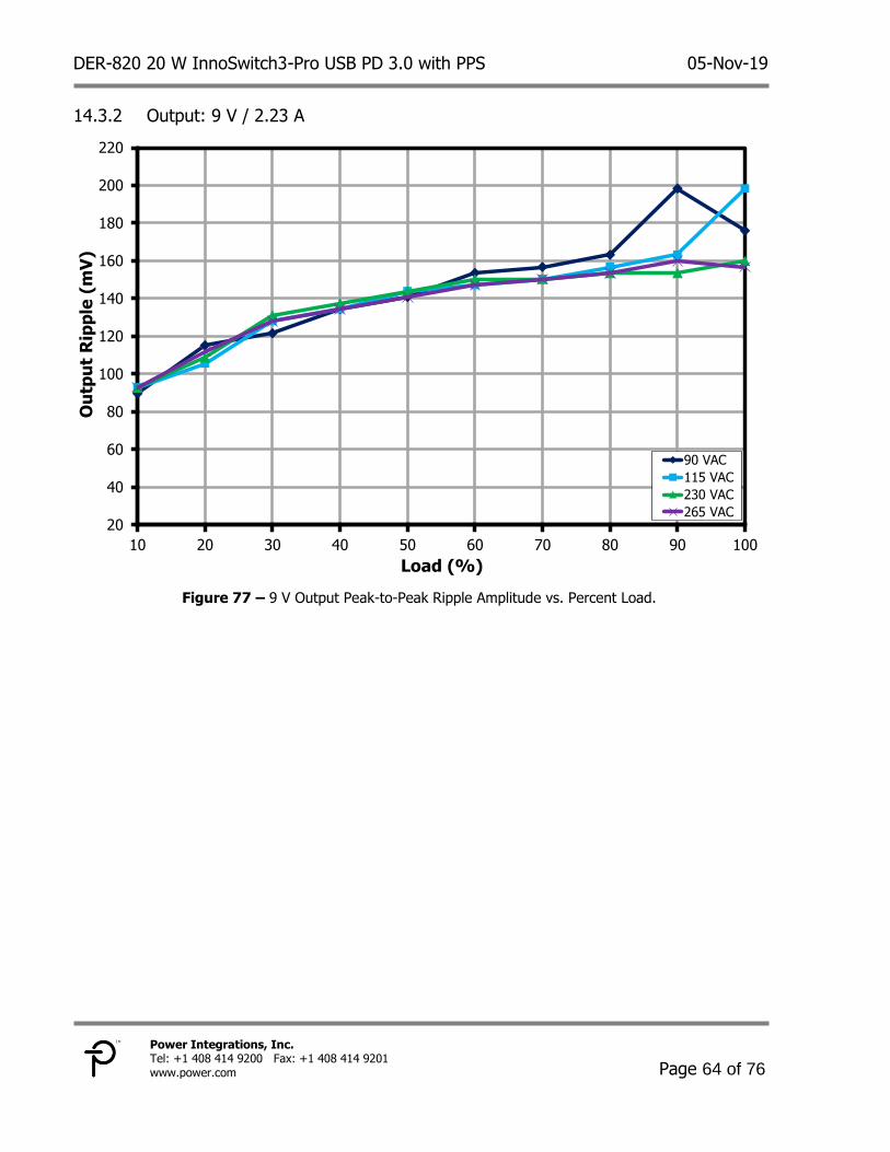
DER-820 20 W InnoSwitch3-Pro USB PD 3.0 with PPS 05-Nov-19
Page 64 of 76
Power Integrations, Inc. Tel: +1 408 414 9200 Fax: +1 408 414 9201 www.power.com
Output: 9 V / 2.23 A 14.3.2
Figure 77 – 9 V Output Peak-to-Peak Ripple Amplitude vs. Percent Load.
20
40
60
80
100
120
140
160
180
200
220
10 20 30 40 50 60 70 80 90 100
Ou
tpu
t R
ipp
le (
mV
)
Load (%)
90 VAC
115 VAC
230 VAC
265 VAC
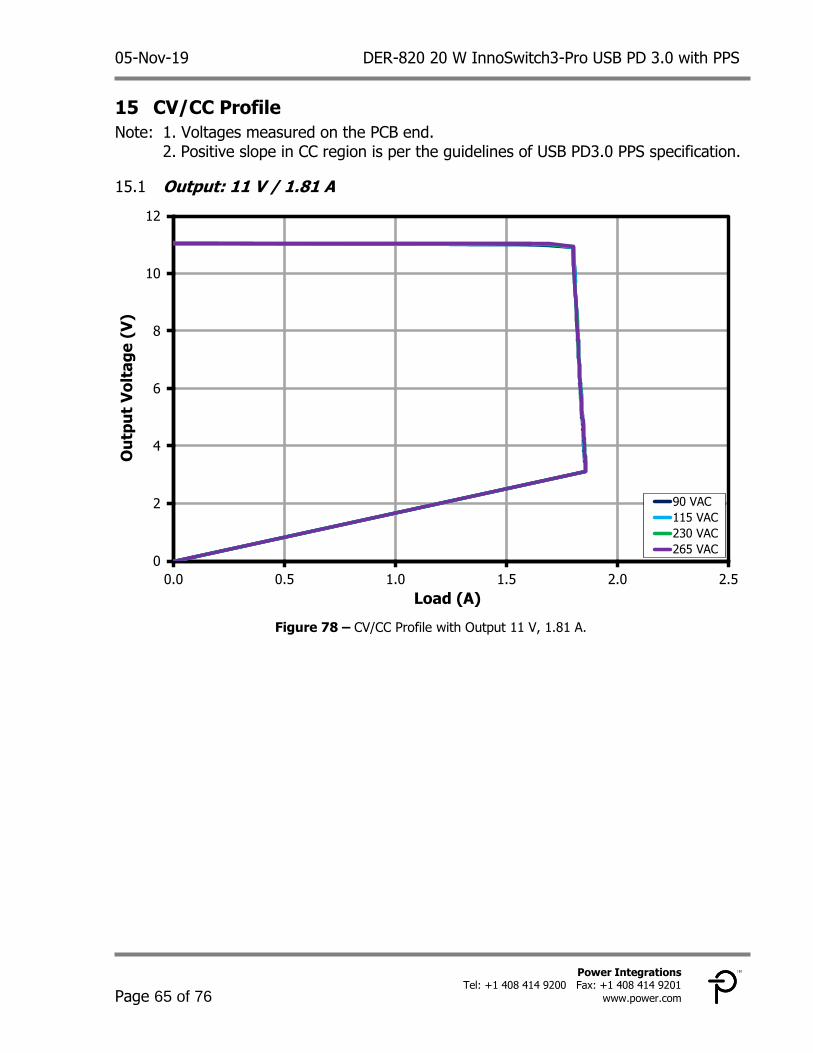
05-Nov-19 DER-820 20 W InnoSwitch3-Pro USB PD 3.0 with PPS
Page 65 of 76
Power Integrations Tel: +1 408 414 9200 Fax: +1 408 414 9201
www.power.com
CV/CC Profile 15
Note: 1. Voltages measured on the PCB end. 2. Positive slope in CC region is per the guidelines of USB PD3.0 PPS specification.
Output: 11 V / 1.81 A 15.1
Figure 78 – CV/CC Profile with Output 11 V, 1.81 A.
0
2
4
6
8
10
12
0.0 0.5 1.0 1.5 2.0 2.5
Ou
tpu
t V
olt
ag
e (
V)
Load (A)
90 VAC
115 VAC
230 VAC
265 VAC
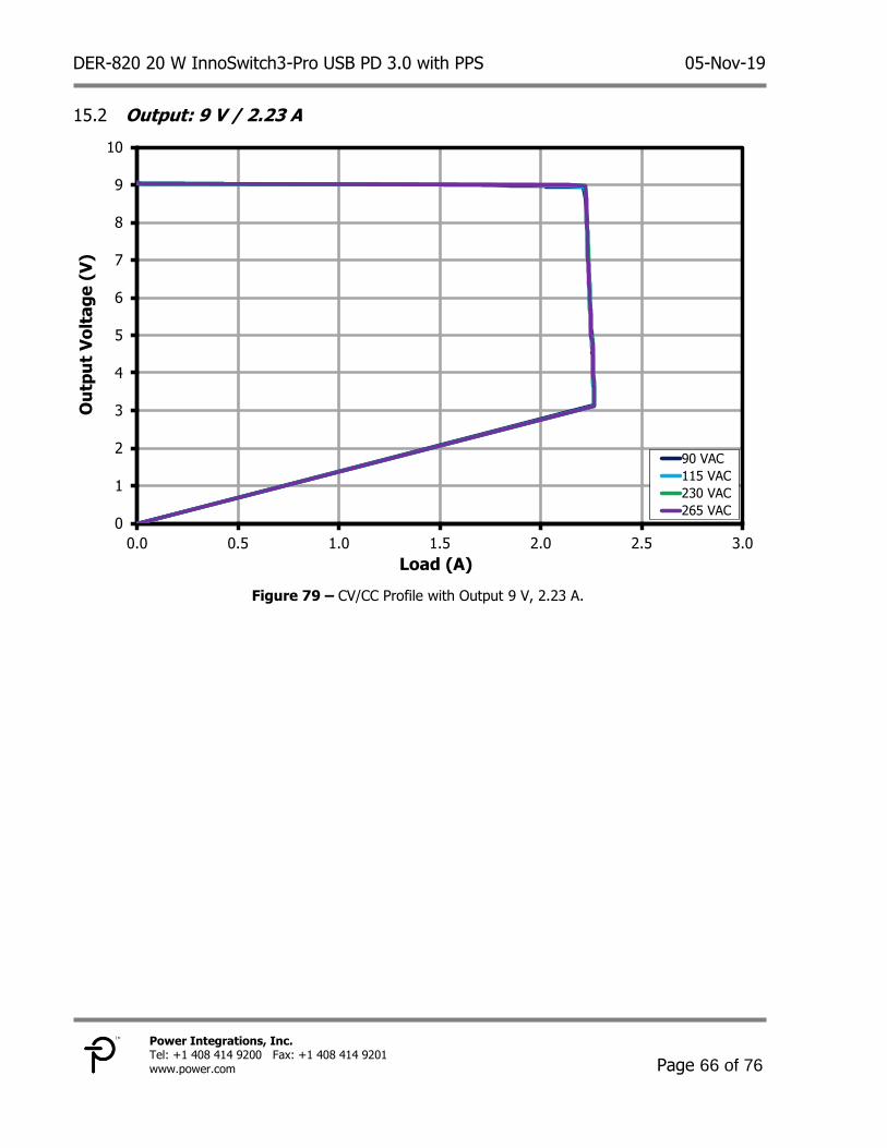
DER-820 20 W InnoSwitch3-Pro USB PD 3.0 with PPS 05-Nov-19
Page 66 of 76
Power Integrations, Inc. Tel: +1 408 414 9200 Fax: +1 408 414 9201 www.power.com
Output: 9 V / 2.23 A 15.2
Figure 79 – CV/CC Profile with Output 9 V, 2.23 A.
0
1
2
3
4
5
6
7
8
9
10
0.0 0.5 1.0 1.5 2.0 2.5 3.0
Ou
tpu
t V
olt
ag
e (
V)
Load (A)
90 VAC
115 VAC
230 VAC
265 VAC

05-Nov-19 DER-820 20 W InnoSwitch3-Pro USB PD 3.0 with PPS
Page 67 of 76
Power Integrations Tel: +1 408 414 9200 Fax: +1 408 414 9201
www.power.com
Output: 5 V / 3 A 15.3
Figure 80 – CV/CC Profile with Output 5 V, 3 A.
0
1
2
3
4
5
6
0.0 0.5 1.0 1.5 2.0 2.5 3.0 3.5 4.0
Ou
tpu
t V
olt
ag
e (
V)
Load (A)
90 VAC
115 VAC
230 VAC
265 VAC

DER-820 20 W InnoSwitch3-Pro USB PD 3.0 with PPS 05-Nov-19
Page 68 of 76
Power Integrations, Inc. Tel: +1 408 414 9200 Fax: +1 408 414 9201 www.power.com
Output: 3.3 V / 3 A 15.4
Figure 81 – CV/CC Profile with Output 3.3 V, 3 A.
0.0
0.5
1.0
1.5
2.0
2.5
3.0
3.5
4.0
0.0 0.5 1.0 1.5 2.0 2.5 3.0 3.5 4.0
Ou
tpu
t V
olt
ag
e (
V)
Load (A)
90 VAC
115 VAC
230 VAC
265 VAC

05-Nov-19 DER-820 20 W InnoSwitch3-Pro USB PD 3.0 with PPS
Page 69 of 76
Power Integrations Tel: +1 408 414 9200 Fax: +1 408 414 9201
www.power.com
Voltage and Current Step Test using Quadramax and Total 16Phase Analyzer
Voltage Step Test (VST) 16.1
Figure 82 – Plot of SPT.6 VST from Total Phase Analyzer.
Current Limit Test (CLT) 16.2
Figure 83 – Plot of SPT.7 CLT from Total Phase Analyzer.
2A 3A 1A
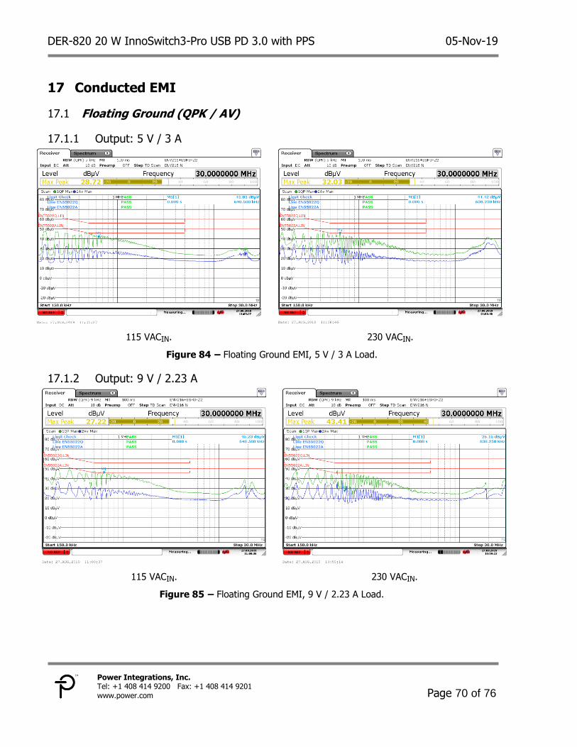
DER-820 20 W InnoSwitch3-Pro USB PD 3.0 with PPS 05-Nov-19
Page 70 of 76
Power Integrations, Inc. Tel: +1 408 414 9200 Fax: +1 408 414 9201 www.power.com
Conducted EMI 17
Floating Ground (QPK / AV) 17.1
Output: 5 V / 3 A 17.1.1
115 VACIN. 230 VACIN.
Figure 84 – Floating Ground EMI, 5 V / 3 A Load.
Output: 9 V / 2.23 A 17.1.2
115 VACIN. 230 VACIN.
Figure 85 – Floating Ground EMI, 9 V / 2.23 A Load.

05-Nov-19 DER-820 20 W InnoSwitch3-Pro USB PD 3.0 with PPS
Page 71 of 76
Power Integrations Tel: +1 408 414 9200 Fax: +1 408 414 9201
www.power.com
Earth Ground (QPK / AV) 17.2
Output: 5 V / 3 A 17.2.1
115 VACIN. 230 VACIN.
Figure 86 – Earth Ground EMI, 5 V / 3 A Load.
Output: 9 V / 2.23 A 17.2.2
115 VACIN. 230 VACIN.
Figure 87 – Earth Ground EMI, 9 V / 2.23 A Load.

DER-820 20 W InnoSwitch3-Pro USB PD 3.0 with PPS 05-Nov-19
Page 72 of 76
Power Integrations, Inc. Tel: +1 408 414 9200 Fax: +1 408 414 9201 www.power.com
Combination Wave Surge 18
The unit was subjected to ±1000 V differential mode combination wave and ±2000 V common mode ring wave surge at several line phase angles with 10 strikes for each condition.
Differential Mode Surge (L1 to L2), 230 VAC Input 18.1
Surge
Level (V)
Injection
Phase (°)
Test Result
5 V / 0 A
Test Result
5 V / 3 A
Test Result
9 V / 0 A
Test Result
9 V / 2.23 A
+1000 0 Pass Pass Pass Pass
-1000 0 Pass Pass Pass Pass
+1000 90 Pass Pass Pass Pass
-1000 90 Pass Pass Pass Pass
+1000 180 Pass Pass Pass Pass
-1000 180 Pass Pass Pass Pass
+1000 270 Pass Pass Pass Pass
-1000 270 Pass Pass Pass Pass
Common Mode Surge (L1 to PE), 230 VAC Input 18.2
Surge
Level (V)
Injection
Phase (°)
Test Result 5 V / 0 A
Test Result 5 V / 3 A
Test Result 9 V / 0 A
Test Result 9 V / 2.23 A
+2000 0 Pass Pass Pass Pass
-2000 0 Pass Pass Pass Pass
+2000 90 Pass Pass Pass Pass
-2000 90 Pass Pass Pass Pass
+2000 180 Pass Pass Pass Pass
-2000 180 Pass Pass Pass Pass
+2000 270 Pass Pass Pass Pass
-2000 270 Pass Pass Pass Pass
Common Mode Surge (L2 to PE), 230 VAC Input 18.3
Surge
Level
(V)
Injection
Phase
(°)
Test Result 5 V / 0 A
Test Result 5 V / 2.23 A
Test Result 9 V / 0 A
Test Result 9 V / 2.23 A
+2000 0 Pass Pass Pass Pass
-2000 0 Pass Pass Pass Pass
+2000 90 Pass Pass Pass Pass
-2000 90 Pass Pass Pass Pass
+2000 180 Pass Pass Pass Pass
-2000 180 Pass Pass Pass Pass
+2000 270 Pass Pass Pass Pass
-2000 270 Pass Pass Pass Pass

05-Nov-19 DER-820 20 W InnoSwitch3-Pro USB PD 3.0 with PPS
Page 73 of 76
Power Integrations Tel: +1 408 414 9200 Fax: +1 408 414 9201
www.power.com
Common Mode Surge (L1, L2 to PE), 230 VAC Input 18.4
Surge
Level (V)
Injection
Phase (°)
Test Result
5 V / 0 A
Test Result
5 V / 3 A
Test Result
9 V / 0 A
Test Result
9 V / 2.23 A
+2000 0 Pass Pass Pass Pass
-2000 0 Pass Pass Pass Pass
+2000 90 Pass Pass Pass Pass
-2000 90 Pass Pass Pass Pass
+2000 180 Pass Pass Pass Pass
-2000 180 Pass Pass Pass Pass
+2000 270 Pass Pass Pass Pass
-2000 270 Pass Pass Pass Pass
Note: Surge events might trigger input line OV Protection and initiate an auto-restart. auto-restart (AR) is one of the safety features of InnoSwitch3-Pro to protect the converter from fault conditions. For applications that require completely no output interruption, the design can be modified to have a higher input line OVP voltage threshold or with the input line OVP completely disabled.
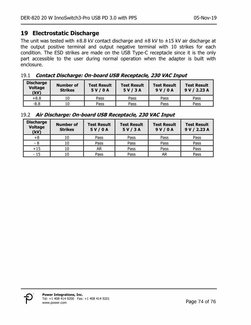
DER-820 20 W InnoSwitch3-Pro USB PD 3.0 with PPS 05-Nov-19
Page 74 of 76
Power Integrations, Inc. Tel: +1 408 414 9200 Fax: +1 408 414 9201 www.power.com
Electrostatic Discharge 19
The unit was tested with ±8.8 kV contact discharge and ±8 kV to ±15 kV air discharge at the output positive terminal and output negative terminal with 10 strikes for each condition. The ESD strikes are made on the USB Type-C receptacle since it is the only part accessible to the user during normal operation when the adapter is built with enclosure.
Contact Discharge: On-board USB Receptacle, 230 VAC Input 19.1
Discharge Voltage
(kV)
Number of Strikes
Test Result 5 V / 0 A
Test Result 5 V / 3 A
Test Result 9 V / 0 A
Test Result 9 V / 2.23 A
+8.8 10 Pass Pass Pass Pass
-8.8 10 Pass Pass Pass Pass
Air Discharge: On-board USB Receptacle, 230 VAC Input 19.2
Discharge
Voltage (kV)
Number of
Strikes
Test Result
5 V / 0 A
Test Result
5 V / 3 A
Test Result
9 V / 0 A
Test Result
9 V / 2.23 A
+8 10 Pass Pass Pass Pass
- 8 10 Pass Pass Pass Pass
+15 10 AR Pass Pass Pass
- 15 10 Pass Pass AR Pass

05-Nov-19 DER-820 20 W InnoSwitch3-Pro USB PD 3.0 with PPS
Page 75 of 76
Power Integrations Tel: +1 408 414 9200 Fax: +1 408 414 9201
www.power.com
Revision History 20
Date Author Revision Description & Changes Reviewed
05-Nov-19 HL 4.0 Initial Release. Apps & Mktg

DER-820 20 W InnoSwitch3-Pro USB PD 3.0 with PPS 05-Nov-19
Page 76 of 76
Power Integrations, Inc. Tel: +1 408 414 9200 Fax: +1 408 414 9201 www.power.com
For the latest updates, visit our website: www.power.com
Reference Designs are technical proposals concerning how to use Power Integrations’ gate drivers in particular applications and/or with certain power modules. These proposals are “as is” and are not subject to any qualification process. The suitability, implementation and qualification are the sole responsibility of the end user. The statements, technical information and recommendations contained herein are believed to be accurate as of the date hereof. All parameters, numbers, values and other technical data included in the technical information were calculated and determined to our best knowledge in accordance with the relevant technical norms (if any). They may base on assumptions or operational conditions that do not necessarily apply in general. We exclude any representation or warranty, express or implied, in relation to the accuracy or completeness of the statements, technical information and recommendations contained herein. No responsibility is accepted for the accuracy or sufficiency of any of the statements, technical information, recommendations or opinions communicated and any liability for any direct, indirect or consequential loss or damage suffered by any person arising therefrom is expressly disclaimed.
Power Integrations reserves the right to make changes to its products at any time to improve reliability or manufacturability. Power Integrations does not assume any liability arising from the use of any device or circuit described herein. POWER INTEGRATIONS MAKES NO WARRANTY HEREIN AND SPECIFICALLY DISCLAIMS ALL WARRANTIES INCLUDING, WITHOUT LIMITATION, THE IMPLIED WARRANTIES OF MERCHANTABILITY, FITNESS FOR A PARTICULAR PURPOSE, AND NON-INFRINGEMENT OF THIRD PARTY RIGHTS.
Patent Information The products and applications illustrated herein (including transformer construction and circuits’ external to the products) may be covered by one or more U.S. and foreign patents, or potentially by pending U.S. and foreign patent applications assigned to Power Integrations. A complete list of Power Integrations’ patents may be found at www.power.com. Power Integrations grants its customers a license under certain patent rights as set forth at http://www.power.com/ip.htm.
Power Integrations, the Power Integrations logo, CAPZero, ChiPhy, CHY, DPA-Switch, EcoSmart, E-Shield, eSIP, eSOP, HiperPLC, HiperPFS, HiperTFS, InnoSwitch, Innovation in Power Conversion, InSOP, LinkSwitch, LinkZero, LYTSwitch, SENZero, TinySwitch, TOPSwitch, PI, PI Expert, SCALE, SCALE-1, SCALE-2, SCALE-3 and SCALE-iDriver, are trademarks of Power Integrations, Inc. Other trademarks are property of their respective companies. ©2019, Power Integrations, Inc.
Power Integrations Worldwide Sales Support Locations
WORLD HEADQUARTERS 5245 Hellyer Avenue San Jose, CA 95138, USA. Main: +1-408-414-9200
Customer Service:
Worldwide: +1-65-635-64480
Americas: +1-408-414-9621 e-mail: [email protected] CHINA (SHANGHAI)
Rm 2410, Charity Plaza, No. 88,
North Caoxi Road,
Shanghai, PRC 200030
Phone: +86-21-6354-6323 e-mail: [email protected] CHINA (SHENZHEN)
17/F, Hivac Building, No. 2, Keji
Nan 8th Road, Nanshan District,
Shenzhen, China, 518057
Phone: +86-755-8672-8689 e-mail: [email protected]
GERMANY (AC-DC/LED Sales)
Einsteinring 24
85609 Dornach/Aschheim
Germany
Tel: +49-89-5527-39100
e-mail: [email protected]
GERMANY (Gate Driver Sales) HellwegForum 1 59469 Ense Germany Tel: +49-2938-64-39990 e-mail: igbt-driver.sales@ power.com INDIA #1, 14th Main Road Vasanthanagar Bangalore-560052 India Phone: +91-80-4113-8020 e-mail: [email protected]
ITALY Via Milanese 20, 3rd. Fl. 20099 Sesto San Giovanni (MI) Italy Phone: +39-024-550-8701 e-mail: [email protected] JAPAN Yusen Shin-Yokohama 1-chome Bldg. 1-7-9, Shin-Yokohama, Kohoku-ku Yokohama-shi, Kanagawa 222-0033 Japan Phone: +81-45-471-1021 e-mail: [email protected] KOREA RM 602, 6FL Korea City Air Terminal B/D, 159-6 Samsung-Dong, Kangnam-Gu, Seoul, 135-728 Korea Phone: +82-2-2016-6610 e-mail: [email protected]
SINGAPORE 51 Newton Road, #19-01/05 Goldhill Plaza Singapore, 308900 Phone: +65-6358-2160 e-mail: [email protected]
TAIWAN
5F, No. 318, Nei Hu Rd., Sec. 1 Nei Hu District Taipei 11493, Taiwan R.O.C. Phone: +886-2-2659-4570 e-mail: [email protected] UK
Building 5, Suite 21
The Westbrook Centre
Milton Road
Cambridge
CB4 1YG
Phone: +44 (0) 7823-557484 e-mail: [email protected]