CY7C65640A, TetraHub™ High-Speed USB Hub Controller
27
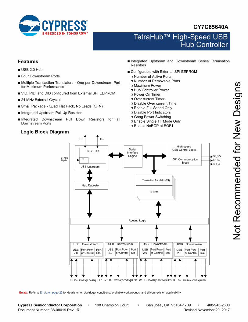
CY7C65640A TetraHub™ High-Speed USB Hub Controller Cypress Semiconductor Corporation • 198 Champion Court • San Jose, CA 95134-1709 • 408-943-2600 Document Number: 38-08019 Rev. *R Revised November 20, 2017 TetraHub™ High-Speed USB Hub Controller Features ■ USB 2.0 Hub ■ Four Downstream Ports ■ Multiple Transaction Translators - One per Downstream Port for Maximum Performance ■ VID, PID, and DID configured from External SPI EEPROM ■ 24 MHz External Crystal ■ Small Package - Quad Flat Pack, No Leads (QFN) ■ Integrated Upstream Pull Up Resistor ■ Integrated Downstream Pull Down Resistors for all Downstream Ports ■ Integrated Upstream and Downstream Series Termination Resistors ■ Configurable with External SPI EEPROM ❐ Number of Active Ports ❐ Number of Removable Ports ❐ Maximum Power ❐ Hub Controller Power ❐ Power On Timer ❐ Over current Timer ❐ Disable Over current Timer ❐ Enable Full Speed Only ❐ Disable Port Indicators ❐ Gang Power Switching ❐ Enable Single TT Mode Only ❐ Enable NoEOP at EOF1 SPI Communication Block USB Upstream USB 2.0 PHY PLL High speed USB Control Logic Serial Interface Engine Hub Repeater Routing Logic D+ D– USB Downstream USB 2.0 Port Pow- er Control Port Sta- D+ D– OVR#[1 LED PWR#[1 Transaction Translator (X4) TT RAM SPI_SD SPI_SCK SPI_CS USB Downstream USB 2.0 Port Pow- er Control Port Sta- D+ D– OVR#[2 LED PWR#[2 USB Downstream USB 2.0 Port Pow- er Control Port Sta- D+ D– OVR#[3 LED PWR#[3 USB Downstream USB 2.0 Port Pow- er Control Port Sta- D+ D– OVR#[4 LED PWR#[4 24 MHz Crystal Logic Block Diagram Errata: Refer to Errata on page 23 for details on errata trigger conditions, available workarounds, and silicon revision applicability. Not Recommended for New Designs
-
Upload
khangminh22 -
Category
Documents
-
view
3 -
download
0
Transcript of CY7C65640A, TetraHub™ High-Speed USB Hub Controller
CY7C65640A
TetraHub™ High-Speed USB Hub Controller
Cypress Semiconductor Corporation • 198 Champion Court • San Jose, CA 95134-1709 • 408-943-2600Document Number: 38-08019 Rev. *R Revised November 20, 2017
TetraHub™ High-Speed USB Hub Controller
Features
■ USB 2.0 Hub
■ Four Downstream Ports
■ Multiple Transaction Translators - One per Downstream Portfor Maximum Performance
■ VID, PID, and DID configured from External SPI EEPROM
■ 24 MHz External Crystal
■ Small Package - Quad Flat Pack, No Leads (QFN)
■ Integrated Upstream Pull Up Resistor
■ Integrated Downstream Pull Down Resistors for allDownstream Ports
■ Integrated Upstream and Downstream Series TerminationResistors
■ Configurable with External SPI EEPROM❐ Number of Active Ports❐ Number of Removable Ports❐ Maximum Power ❐ Hub Controller Power❐ Power On Timer❐ Over current Timer❐ Disable Over current Timer❐ Enable Full Speed Only❐ Disable Port Indicators❐ Gang Power Switching❐ Enable Single TT Mode Only❐ Enable NoEOP at EOF1
SPI CommunicationBlock
USB Upstream
USB 2.0 PHY
PLL
High speedUSB Control LogicSerial
InterfaceEngine
Hub Repeater
Routing Logic
D+ D–
USB Downstream
USB 2.0
Port Pow-er Control
PortSta-
D+ D– OVR#[1LEDPWR#[1
Transaction Translator (X4)
TT RAM
SPI_SD
SPI_SCK
SPI_CS
USB Downstream
USB 2.0
Port Pow-er Control
PortSta-
D+ D– OVR#[2LEDPWR#[2
USB Downstream
USB 2.0
Port Pow-er Control
PortSta-
D+ D– OVR#[3LEDPWR#[3
USB Downstream
USB 2.0
Port Pow-er Control
PortSta-
D+ D– OVR#[4LEDPWR#[4
24 MHzCrystal
Logic Block Diagram
Errata: Refer to Errata on page 23 for details on errata trigger conditions, available workarounds, and silicon revision applicability.
Not
Rec
omm
ende
d fo
r New
Des
igns
CY7C65640A
Document Number: 38-08019 Rev. *R Page 2 of 27
Functional Description
Cypress’s TetraHub is a high performance self poweredUniversal Serial Bus (USB) 2.0 hub. The Tetra architectureprovides four downstream USB ports, with a TransactionTranslator (TT) for each port, making it the highest performinghub possible. This single-chip device incorporates one upstreamand four downstream USB transceivers, a serial InterfaceEngine (SIE), USB hub controller and repeater, and four TTs. Itis suitable for standalone hubs, motherboard hubs, and monitorhub applications.
Being a fixed-function USB device, there is no risk or addedengineering effort required for firmware development. Thedeveloper does not need to write any firmware for their design.The CY4602 Tetrahub USB 2.0 4-port Hub Reference Design Kitprovides all materials and documents needed to move rapidlyinto production. The reference design kit includes boardschematics, bill of materials, Gerber files, Orcad files, keyapplication notes, and product description.
CY7C65640A-LFXC is a functional and pin equivalent dierevision of Cypress’s CY7C65640-LFXC. Changes were madeto improve device performance.
TetraHub Architecture
The Logic Block Diagram on page 1 shows the TetraHubArchitecture.
USB Serial Interface Engine (SIE)
The SIE enables the CY7C65640A to communicate with theUSB host through the USB repeater component of the hub. TheSIE handles the following USB bus activity independently of theHub Control Block:
■ Bit stuffing/unstuffing
■ Checksum generation/checking
■ ACK/NAK/STALL
■ TOKEN type identification
■ Address checking.
Hub Controller
The hub control block does the following protocol handling at ahigher level:
■ Coordinate enumeration by responding to SETUP packets
■ Fill and empty the FIFOs
■ Suspend/Resume coordination
■ Verify and select DATA toggle values
■ Port power control and over current detection.
The Hub controller provides status and control and permits hostaccess to the hub.
Hub Repeater
The hub repeater manages the connectivity between upstreamand downstream facing ports that are operating at the samespeed. It supports full/low speed connectivity and high speedconnectivity. According to USB 2.0 specification, the hubrepeater provides the following functions:
■ Sets up and tears down connectivity on packet boundaries
■ Ensures orderly entry into and out of the suspend state,including proper handling of remote wake ups.
Transaction Translator
The TT translates data from one speed to another. A TT takeshigh speed split transactions and translates them to full/lowspeed transactions when the hub is operating at high speed (theupstream port is connected to a high speed host controller) andhas full/low speed devices attached. The operating speed of adevice attached on a downstream facing port determineswhether the routing logic connects a port to the transactiontranslator or hub repeater section. If a low or full speed device isconnected to the hub operating at high speed, the data transferroute includes the transaction translator. If a high speed deviceis connected to this high speed hub the route only includes therepeater and no transaction translator; the device and the hubare in conformation with respect to their data transfer speed.When the hub is operating at full speed (the upstream port isconnected to a full speed host controller), a high speedperipheral does not operate at its full capability. These devicesonly work at 1.1 speed. Full and low speed devices connected tothis hub operate at their 1.1 speed.
Applications
■ Standalone Hubs
■ Motherboard Hubs
■ Monitor Hub applications
■ External Personal Storage Drives
■ Port Replicators
■ Portable Drive
■ Docking Stations
Not
Rec
omm
ende
d fo
r New
Des
igns
CY7C65640A
Document Number: 38-08019 Rev. *R Page 3 of 27
Contents
Introduction .......................................................................3TetraHub Architecture ................................................. 3USB Serial Interface Engine (SIE) .............................. 3Hub Controller ............................................................. 3Hub Repeater .............................................................. 3Transaction Translator ................................................ 3
Applications ...................................................................... 3Functional Overview ........................................................ 4
System Initialization ..................................................... 4Enumeration ................................................................ 4Multiple Transaction Translator Support ..................... 4Downstream Ports ....................................................... 4Upstream Port ............................................................. 4Power Switching .......................................................... 4Over current Detection ................................................ 5Port Indicators ............................................................. 5
Pin Configuration ............................................................. 6Default Descriptors .......................................................... 9
Device Descriptor ........................................................ 9Configuration Options ................................................... 12
Default – 0xD0 Load .................................................. 12Configured – 0xD2 Load ........................................... 12
Supported USB Requests .............................................. 13Device Class Commands .......................................... 13Hub Class Commands .............................................. 14
Upstream USB Connection ............................................ 15Downstream USB Connections ..................................... 16LED Connections ............................................................ 16Sample Schematic .......................................................... 17Maximum Ratings ........................................................... 18Operating Conditions ..................................................... 18DC Electrical Characteristics ........................................ 18AC Electrical Characteristics ........................................ 19Ordering Information ...................................................... 20
Ordering Code Definitions ......................................... 20Package Diagram ............................................................ 21
Quad Flat Package No Leads (QFN) Package Design Notes ..................................................... 22Document History Page ................................................. 24Sales, Solutions, and Legal Information ...................... 26
Worldwide Sales and Design Support ....................... 26Products .................................................................... 26PSoC® Solutions ...................................................... 26Cypress Developer Community ................................. 26Technical Support ..................................................... 26
Not
Rec
omm
ende
d fo
r New
Des
igns
CY7C65640A
Document Number: 38-08019 Rev. *R Page 4 of 27
Functional Overview
The Cypress TetraHub USB 2.0 hub is a high performance,low-system-cost solution for USB. This hub integrates 1.5kupstream pull up resistors for full speed operation and alldownstream 15k pull down resistors and series terminationresistors on all upstream and downstream D+ and D– pins. Thisresults in optimization of system costs by providing built-insupport for the USB 2.0 specification.
System Initialization
On power up, the TetraHub reads an external SPI EEPROM forconfiguration information. At the most basic level, this EEPROMhas the Vendor ID (VID), Product ID (PID), and Device ID (DID)for the customer’s application. For more specializedapplications, other configuration options can be specified. SeeConfiguration Options on page 12 for more details.
After reading the EEPROM, if BUSPOWER (connected to theupstream VBus) is high, TetraHub enables the pull up resistor onthe D+ to indicate that it is connected to the upstream hub, afterwhich a USB bus reset is expected. During this reset, TetraHubinitiates a chirp to indicate that it is a high speed peripheral. In aUSB 2.0 system, the upstream hub responds with a chirpsequence, and TetraHub is in a high speed mode, with theupstream D+ pull up resistor turned off. In USB 1.x systems, nosuch chirp sequence from the upstream hub is seen, andTetraHub operates as a normal 1.x hub (operating at full speed).
Enumeration
After a USB Bus Reset, TetraHub is in an unaddressed,non-configured state (configuration value set to 0). During theenumeration process, the host sets the hub’s address andconfiguration by sending a SetCongfiguration request. Changingthe hub address restores it to an non-configured state.
For high speed multi-TT support, the host must also set thealternate interface setting to 1 (the default mode is single TT).After the hub is configured, the full hub functionality is available.
Multiple Transaction Translator Support
After TetraHub is configured in a high speed system, it is in singleTT mode. The host may then set the hub into multiple TT modeby sending a SetInterface command. In multiple TT mode, eachfull speed port is handled independently and thus has a full 12 Mbps bandwidth available. In Single TT mode, all traffic fromthe host destined for full or low speed ports are forwarded to allof those ports. This means that the 12 Mbps bandwidth is sharedby all full and low speed ports.
Downstream Ports
TetraHub supports a maximum of four downstream ports, eachof which may be marked as usable or removable in the extendedconfiguration (0xD2 EEPROM load, see section). DownstreamD+ and D– pull down resistors are incorporated in TetraHub foreach port. Prior to the hub being configured, the ports are drivenSE0 (Single Ended Zero, where both D+ and D– are driven low)and are set to the non-powered state.
After the hub is configured, the ports are not driven, and the hostmay power the ports by sending a SetPortPower command toeach port. After a port is powered, any connect or disconnectevent is detected by the hub. Any change in the port state isreported by the hub back to the host through the Status ChangeEndpoint (endpoint 1). Upon receipt of SetPortReset commandfrom the host, the hub does the following:
■ Drive SE0 on the corresponding port
■ Put the port in an enabled state
■ Enable the green port indicator for that port (if not previouslyoverridden by the host)
■ Enable babble detection after the port is enabled.
Babble consists of either non-terminated traffic from adownstream port (or loss of activity), or a non-idle condition onthe port after EOF2. If babble is detected on an enabled port, thatport is disabled. A ClearPortEnable command from the host alsodisables the specified port.
Downstream ports can be individually suspended by the hostwith the SetPortSuspend command. If the hub is not suspended,any resume will be confined to that individual port and reflectedto the host through a port change indication in the Hub StatusChange Endpoint. If the hub is suspended, a resume on this portwill be forwarded to the host, but other resume events will not beseen on that port. The host may resume the port by sending aClearPortSuspend command.
Upstream Port
The upstream port includes the transmitter and the receiver statemachine. The transmitter and receiver operate in high speed andfull speed depending on the current hub configuration.
The transmitter state machine monitors the upstream facing portwhile the hub repeater has connectivity in the upstream direction.This monitoring activity prevents propagation of erroneousindications in the upstream direction. In particular, this machineprevents babble and disconnect events on the downstreamfacing ports of this hub from propagating and causing the hub tobe disabled or disconnected by the hub to which it is attached.This enables the hub to only disconnect the offensive port ondetecting a babble from it.
Power Switching
TetraHub includes interface signals for external port powerswitches. Both ganged and individual (for each port)configurations are supported, with individual switching being thedefault. Initially all ports are non-powered. After enumerating, thehost may power each port by sending a SetPortPower commandfor that port. The power switching and over current detection ofdownstream ports is managed by control pins connected to anexternal power switch device. PWR [n]# output pins of theCY7C65640A series are connected to the respective externalpower switch's port power enable signals. (Note that each portpower output pin of the external power switch must be bypassedwith an electrolytic or tantalum capacitor as required by the USBspecification. These capacitors supply the inrush currents, whichoccur during downstream device hot-attach events.)
Not
Rec
omm
ende
d fo
r New
Des
igns
CY7C65640A
Document Number: 38-08019 Rev. *R Page 5 of 27
Over current Detection
Over current detection includes timed detection of 8 ms bydefault. This parameter is configured from the external EEPROMin a range of 0 ms to 15 ms for both an enabled port and adisabled port individually. Detection of over on downstream portsis managed by control pins connected to an external powerswitch device.
The OVR[n]# pins of the CY7C65640A series are connected tothe respective external power switch’s port over currentindication (output) signals. Upon detecting an over currentcondition, the hub device reports the over current condition to thehost and disables the PWR# output to the external power device.
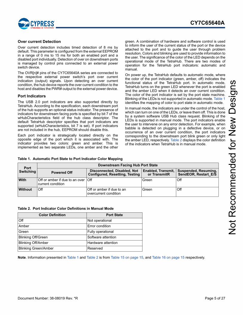
Port Indicators
The USB 2.0 port indicators are also supported directly byTetraHub. According to the specification, each downstream portof the hub supports an optional status indicator. The presence ofindicators for downstream facing ports is specified by bit 7 of thewHubCharacteristics field of the hub class descriptor. Thedefault TetraHub descriptor specifies that port indicators aresupported (wHubCharacteristics, bit 7 is set). If port indicatorsare not included in the hub, EEPROM should disable this.
Each port indicator is strategically located directly on theopposite edge of the port which it is associated with. Theindicator provides two colors: green and amber. This isimplemented as two separate LEDs, one amber and the other
green. A combination of hardware and software control is usedto inform the user of the current status of the port or the deviceattached to the port and to guide the user through problemresolution. Colors and blinking are used to provide information tothe user. The significance of the color of the LED depends on theoperational mode of the TetraHub. There are two modes ofoperation for the TetraHub port indicators: automatic andmanual.
On power up, the TetraHub defaults to automatic mode, wherethe color of the port indicator (green, amber, off) indicates thefunctional status of the TetraHub port. In automatic mode,TetraHub turns on the green LED whenever the port is enabledand the amber LED when it detects an over current condition.The color of the port indicator is set by the port state machine.Blinking of the LEDs is not supported in automatic mode. Table 1identifies the mapping of color to port state in automatic mode.
In manual mode, the indicators are under the control of the host,which can turn on one of the LEDs, or leave them off. This is doneby a system software USB Hub class request. Blinking of theLEDs is supported in manual mode. The port indicators enablethe user to intervene on any error detection. For example, whenbabble is detected on plugging in a defective device, or onoccurrence of an over current condition, the port indicatorscorresponding to the downstream port blink green or only lightthe amber LED, respectively. Table 2 displays the color definitionof the indicators when TetraHub is in manual mode.
Note. Information presented in Table 1 and Table 2 is from Table 15 on page 15, and Table 16 on page 15 respectively.
Table 1. Automatic Port State to Port Indicator Color Mapping
Port Switching
Downstream Facing Hub Port State
Powered Off Disconnected, Disabled, Not Configured, Resetting, Testing
Enabled, Transmit, or TransmitR
Suspended, Resuming, SendEOR, Restart_E/S
With Off or amber if due to an over current condition
Off Green Off
Without Off Off or amber if due to an overcurrent condition
Green Off
Table 2. Port Indicator Color Definitions in Manual Mode
Color Definition Port State
Off Not operational
Amber Error condition
Green Fully operational
Blinking Off/Green Software attention
Blinking Off/Amber Hardware attention
Blinking Green/Amber Reserved
Not
Rec
omm
ende
d fo
r New
Des
igns
CY7C65640A
Document Number: 38-08019 Rev. *R Page 6 of 27
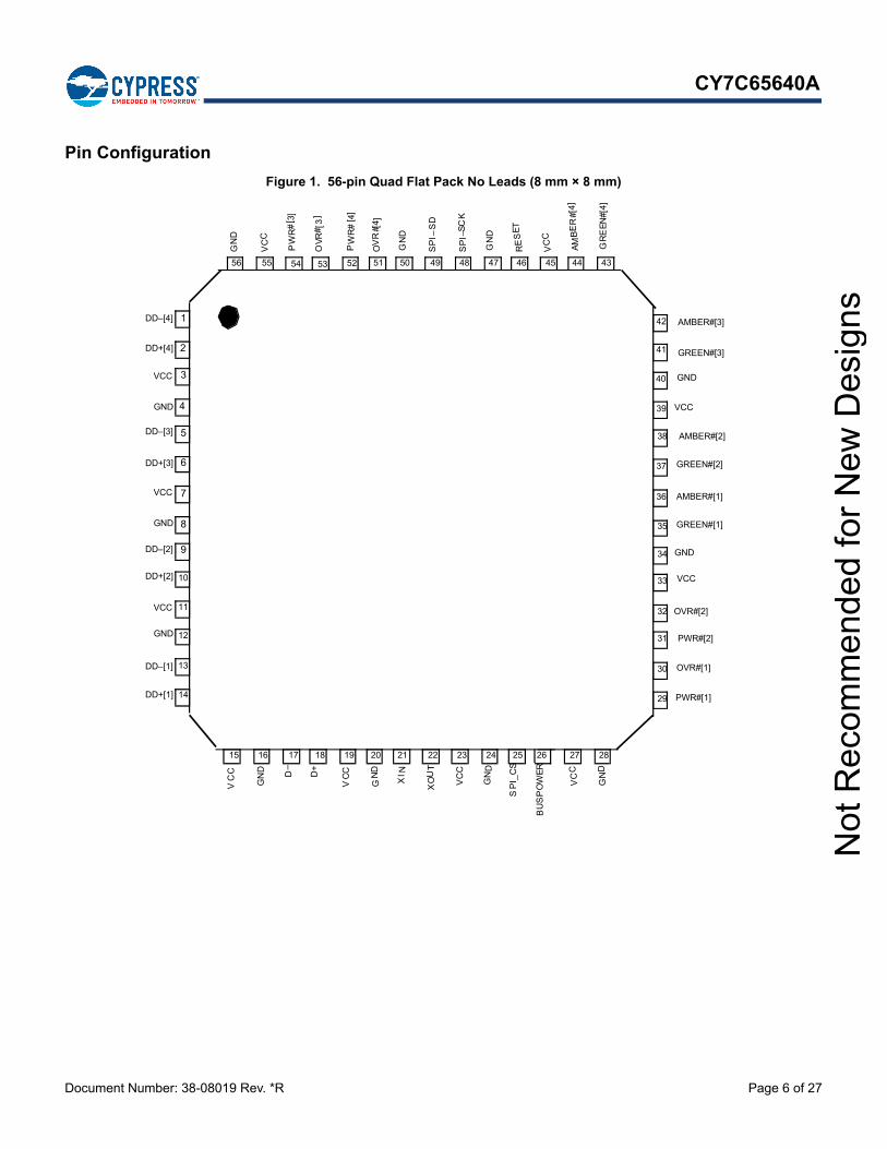
Pin Configuration
Figure 1. 56-pin Quad Flat Pack No Leads (8 mm × 8 mm)
VCC
VC
C
VC
C
GN
D
GN
D
GN
D
BU
SP
OW
ER
GREEN#[1]
AMBER#[1]
GREEN#[2]
AMBER#[2]
GREEN#[3]
AMBER#[3]
AM
BE
R#[
4]
GR
EE
N#[
4]
1
2
3
4
5
6
7
8
9
545556 53 52 51 50 49 48 47 46 45 44 43
42
41
40
39
38
37
36
35
34
33
32
31
30
29
2827262524232221201918171615
14
13
12
11
10
DD–[4]
DD+[4]
VCC
GND
DD–[3]
DD+[3]
VCC
GND
DD–[2]
DD+[2]
VCC
GND
DD–[1]
DD+[1]
VC
C
VC
C
VC
C
VC
CVCC
GN
D
GN
D
GN
D
GN
D
GND
GND
D–
D+
XI N
XO
UT
SP
I_C
S
PWR#[1]
OVR#[1]
PWR#[2]
OVR#[2]
RE
SE
T
SP
I_ SC
K
SP
I_S
D
PW
R#
[ 3]
OV
R# [
3]
PW
R#
[ 4]
OV
R#[
4 ]
Not
Rec
omm
ende
d fo
r New
Des
igns
CY7C65640A
Document Number: 38-08019 Rev. *R Page 7 of 27
Pin Definitions
Table 3. CY7C65640A Pin Assignments
Pin Name Type Default Description
3 VCC Power N/A VCC. This signal provides power to the chip.
7 VCC Power N/A VCC. This signal provides power to the chip.
11 VCC Power N/A VCC. This signal provides power to the chip.
15 VCC Power N/A VCC. This signal provides power to the chip.
19 VCC Power N/A VCC. This signal provides power to the chip.
23 VCC Power N/A VCC. This signal provides power to the chip.
27 VCC Power N/A VCC. This signal provides power to the chip.
33 VCC Power N/A VCC. This signal provides power to the chip.
39 VCC Power N/A VCC. This signal provides power to the chip.
45 VCC Power N/A VCC. This signal provides power to the chip.
55 VCC Power N/A VCC. This signal provides power to the chip.
4 GND Power N/A GND. Connect to Ground with as short a path as possible.
8 GND Power N/A GND. Connect to Ground with as short a path as possible.
12 GND Power N/A GND. Connect to Ground with as short a path as possible.
16 GND Power N/A GND. Connect to Ground with as short a path as possible.
20 GND Power N/A GND. Connect to Ground with as short a path as possible.
24 GND Power N/A GND. Connect to Ground with as short a path as possible.
28 GND Power N/A GND. Connect to Ground with as short a path as possible.
34 GND Power N/A GND. Connect to Ground with as short a path as possible.
40 GND Power N/A GND. Connect to Ground with as short a path as possible.
47 GND Power N/A GND. Connect to Ground with as short a path as possible.
50 GND Power N/A GND. Connect to Ground with as short a path as possible.
56 GND Power N/A GND. Connect to Ground with as short a path as possible.
21 XIN Input N/A 24 MHz Crystal IN or External Clock Input.
22 XOUT Output N/A 24 MHz Crystal OUT.
46 RESET# Input N/A Active LOW Reset. This pin resets the entire chip. It is normally tied to VCC through a 100K resistor, and to GND through a 0.1 µF capacitor. Other than this, no other special power up procedure is required.
26 BUSPOWER Input N/A VBUS. Connect to the VBUS pin of the upstream connector. This signal indicates to the hub that it is in a powered state, and may enable the D+ pull up resistor to indicate a connection. (The hub does so after the external EEPROM is read, unless it is put into a high speed mode by the upstream hub). The hub cannot be bus powered, and the VBUS signal must not be used as a power source.
SPI INTERFACE
25 SPI_CS O O SPI Chip Select. Connect to CS pin of the EEPROM.
48 SPI_SCK O O SPI Clock. Connect to EEPROM SCK pin.
49 SPI_SD I/O/Z Z SPI Dataline Connect to GND with 15 Kresistor and to the Data I/O pins of the EEPROM.
UPSTREAM PORT
17 D– I/O/Z Z Upstream D– Signal.
18 D+ I/O/Z Z Upstream D+ Signal.
Not
Rec
omm
ende
d fo
r New
Des
igns
CY7C65640A
Document Number: 38-08019 Rev. *R Page 8 of 27
Unused port DD+/DD– lines can be left floating. The port power, amber, and green LED pins should be left unconnected, and the overcurrent pin should be tied high. The over current pin is an input and it should not be left floating.
DOWNSTREAM PORT 1
13 DD–[1] I/O/Z Z Downstream D– Signal.
14 DD+[1] I/O/Z Z Downstream D+ Signal.
36 AMBER#[1] O 1 LED. Driver output for amber LED. Port Indicator Support. Active LOW.
35 GREEN#[1] O 1 LED. Driver output for green LED. Port Indicator Support. Active LOW.
30 OVR#[1] Input 1 Overcurrent Condition Detection Input. Active LOW.
29 PWR#[1] O/Z Z Power Switch Driver Output. Active LOW.
DOWNSTREAM PORT 2
9 DD–[2] I/O/Z Z Downstream D– Signal.
10 DD+[2] I/O/Z Z Downstream D+ Signal.
38 AMBER#[2] O 1 LED. Driver output for amber LED. Port Indicator Support. Active LOW.
37 GREEN#[2] O 1 LED. Driver output for green LED. Port Indicator Support. Active LOW.
32 OVR#[2] Input 1 Overcurrent Condition Detection Input. Active LOW.
31 PWR#[2] O/Z Z Power Switch Driver Output. Active LOW.
DOWNSTREAM PORT 3
5 DD–[3] I/O/Z Z Downstream D– Signal.
6 DD+[3] I/O/Z Z Downstream D+ Signal.
42 AMBER#[3] O 1 LED. Driver output for Amber LED. Port Indicator Support. Active LOW.
41 GREEN#[3] O 1 LED. Driver output for Green LED. Port Indicator Support. Active LOW.
53 OVR#[3] Input 1 Overcurrent Condition Detection Input. Active LOW.
54 PWR#[3] O/Z Z Power Switch Driver Output. Active LOW.
DOWNSTREAM PORT 4
1 DD–[4] I/O/Z Z Downstream D– Signal.
2 DD+[4] I/O/Z Z Downstream D+ Signal.
44 AMBER#[4] O 1 LED. Driver output for Amber LED. Port Indicator Support. Active LOW.
43 GREEN#[4] O 1 LED. Driver output for Green LED. Port Indicator Support. Active LOW.
51 OVR#[4] Input 1 Overcurrent Condition Detection Input. Active LOW.
52 PWR#[4] O/Z Z Power Switch Driver Output. Active LOW.
Table 3. CY7C65640A Pin Assignments (continued)
Pin Name Type Default Description
Not
Rec
omm
ende
d fo
r New
Des
igns
CY7C65640A
Document Number: 38-08019 Rev. *R Page 9 of 27
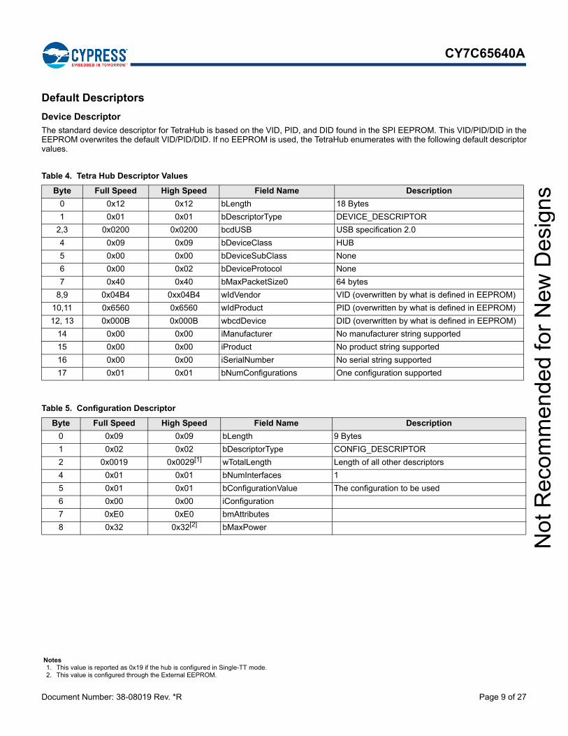
Default Descriptors
Device Descriptor
The standard device descriptor for TetraHub is based on the VID, PID, and DID found in the SPI EEPROM. This VID/PID/DID in theEEPROM overwrites the default VID/PID/DID. If no EEPROM is used, the TetraHub enumerates with the following default descriptorvalues.
Table 4. Tetra Hub Descriptor Values
Byte Full Speed High Speed Field Name Description
0 0x12 0x12 bLength 18 Bytes
1 0x01 0x01 bDescriptorType DEVICE_DESCRIPTOR
2,3 0x0200 0x0200 bcdUSB USB specification 2.0
4 0x09 0x09 bDeviceClass HUB
5 0x00 0x00 bDeviceSubClass None
6 0x00 0x02 bDeviceProtocol None
7 0x40 0x40 bMaxPacketSize0 64 bytes
8,9 0x04B4 0xx04B4 wIdVendor VID (overwritten by what is defined in EEPROM)
10,11 0x6560 0x6560 wIdProduct PID (overwritten by what is defined in EEPROM)
12, 13 0x000B 0x000B wbcdDevice DID (overwritten by what is defined in EEPROM)
14 0x00 0x00 iManufacturer No manufacturer string supported
15 0x00 0x00 iProduct No product string supported
16 0x00 0x00 iSerialNumber No serial string supported
17 0x01 0x01 bNumConfigurations One configuration supported
Table 5. Configuration Descriptor
Byte Full Speed High Speed Field Name Description
0 0x09 0x09 bLength 9 Bytes
1 0x02 0x02 bDescriptorType CONFIG_DESCRIPTOR
2 0x0019 0x0029[1] wTotalLength Length of all other descriptors
4 0x01 0x01 bNumInterfaces 1
5 0x01 0x01 bConfigurationValue The configuration to be used
6 0x00 0x00 iConfiguration
7 0xE0 0xE0 bmAttributes
8 0x32 0x32[2] bMaxPower
Notes1. This value is reported as 0x19 if the hub is configured in Single-TT mode.2. This value is configured through the External EEPROM.
Not
Rec
omm
ende
d fo
r New
Des
igns
CY7C65640A
Document Number: 38-08019 Rev. *R Page 10 of 27
Table 6. Interface Descriptor
Byte Full Speed High Speed Field Name Description
0 0x09 0x09 bLength 9 Bytes
1 0x04 0x04 bDescriptorType INTERFACE_DESCRIPTOR
2 0x00 0x00 bInterfaceNumber
3 0x00 0x00 bAlternateSetting
4 0x01 0x01 bNumEndpoints
5 0x09 0x09 bInterfaceClass
6 0x00 0x00 bInterfaceSubClass
7 0x00 0x01 bInterfaceProtocol
8 0x00 0x00 iInterface
Table 7. Endpoint Descriptor
Byte Full Speed High Speed Field Name Description
0 0x07 0x07 bLength 7 Bytes
1 0x05 0x05 bDescriptorType ENDPOINT_DESCRIPTOR
2 0x81 0x81 bEndpointAddress IN Endpoint #1
3 0x03 0x03 bmAttributes Interrupt
4,5 0x0001 0x0001 wMaxPacketSize Maximum packet size
6 0xFF 0x0C bInterval Polling rate
Table 8. Interface Descriptor [3]
Byte Full Speed High Speed Field Name Description
0 N/A 0x09 bLength 9 Bytes
1 N/A 0x04 bDescriptorType INTERFACE_DESCRIPTOR
2 N/A 0x00 bInterfaceNumber Interface descriptor index
3 N/A 0x01 bAlternateSetting Alternate setting for the interface
4 N/A 0x01 bNumEndpoints Number of endpoints defined
5 N/A 0x09 bInterfaceClass Interface class
6 N/A 0x00 bInterfaceSubClass Interface sub-class
7 N/A 0x02 bInterfaceProtocol Interface protocol
8 N/A 0x00 bInterface Interface string index
Table 9. Endpoint Descriptor [3]
Byte Full Speed High Speed Field Name Description
0 N/A 0x07 bLength 7 Bytes
1 N/A 0x05 bDescriptorType ENDPOINT_DESCRIPTOR
2 N/A 0x81 bEndpointAddress IN Endpoint #1
3 N/A 0x03 bmAttributes Interrupt
4,5 N/A 0x0001 wMaxPacketSize Maximum packet size
6 N/A 0x0C bInterval Polling rate
Note3. If TetraHub is configured for single-TT only (from the external EEPROM), this descriptor is not present.
Not
Rec
omm
ende
d fo
r New
Des
igns
CY7C65640A
Document Number: 38-08019 Rev. *R Page 11 of 27
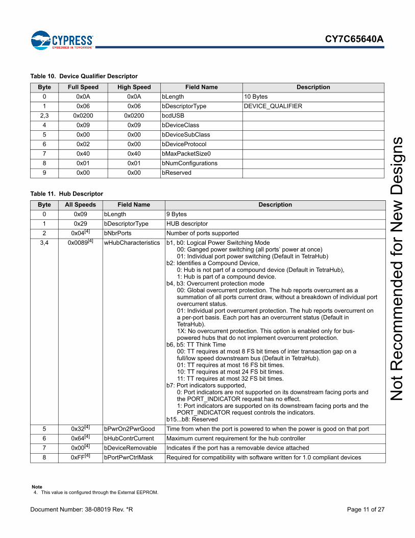
Table 10. Device Qualifier Descriptor
Byte Full Speed High Speed Field Name Description
0 0x0A 0x0A bLength 10 Bytes
1 0x06 0x06 bDescriptorType DEVICE_QUALIFIER
2,3 0x0200 0x0200 bcdUSB
4 0x09 0x09 bDeviceClass
5 0x00 0x00 bDeviceSubClass
6 0x02 0x00 bDeviceProtocol
7 0x40 0x40 bMaxPacketSize0
8 0x01 0x01 bNumConfigurations
9 0x00 0x00 bReserved
Table 11. Hub Descriptor
Byte All Speeds Field Name Description
0 0x09 bLength 9 Bytes
1 0x29 bDescriptorType HUB descriptor
2 0x04[4] bNbrPorts Number of ports supported
3,4 0x0089[4] wHubCharacteristics b1, b0: Logical Power Switching Mode00: Ganged power switching (all ports’ power at once)01: Individual port power switching (Default in TetraHub)
b2: Identifies a Compound Device, 0: Hub is not part of a compound device (Default in TetraHub), 1: Hub is part of a compound device.
b4, b3: Overcurrent protection mode00: Global overcurrent protection. The hub reports overcurrent as a summation of all ports current draw, without a breakdown of individual portovercurrent status.01: Individual port overcurrent protection. The hub reports overcurrent on a per-port basis. Each port has an overcurrent status (Default in TetraHub).1X: No overcurrent protection. This option is enabled only for bus-powered hubs that do not implement overcurrent protection.
b6, b5: TT Think Time00: TT requires at most 8 FS bit times of inter transaction gap on a full/low speed downstream bus (Default in TetraHub).01: TT requires at most 16 FS bit times.10: TT requires at most 24 FS bit times. 11: TT requires at most 32 FS bit times.
b7: Port indicators supported, 0: Port indicators are not supported on its downstream facing ports and the PORT_INDICATOR request has no effect. 1: Port indicators are supported on its downstream facing ports and the PORT_INDICATOR request controls the indicators.
b15...b8: Reserved
5 0x32[4] bPwrOn2PwrGood Time from when the port is powered to when the power is good on that port
6 0x64[4] bHubContrCurrent Maximum current requirement for the hub controller
7 0x00[4] bDeviceRemovable Indicates if the port has a removable device attached
8 0xFF[4] bPortPwrCtrlMask Required for compatibility with software written for 1.0 compliant devices
Note4. This value is configured through the External EEPROM.
Not
Rec
omm
ende
d fo
r New
Des
igns
CY7C65640A
Document Number: 38-08019 Rev. *R Page 12 of 27
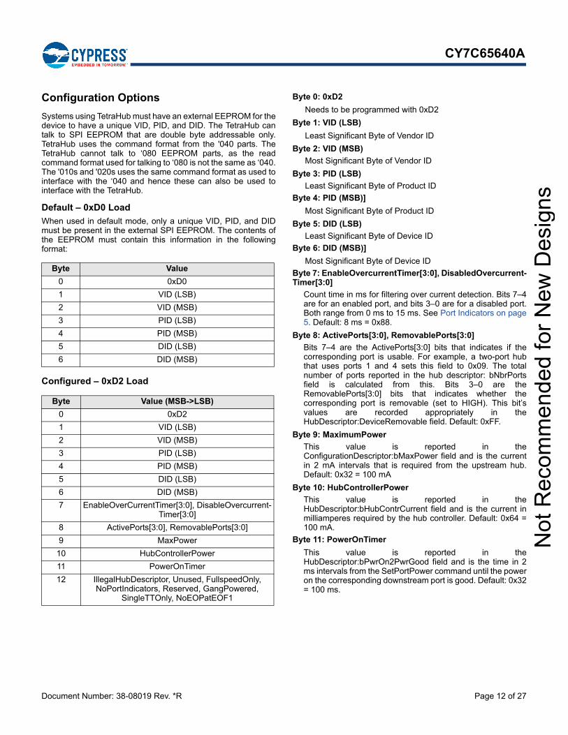
Configuration Options
Systems using TetraHub must have an external EEPROM for thedevice to have a unique VID, PID, and DID. The TetraHub cantalk to SPI EEPROM that are double byte addressable only.TetraHub uses the command format from the '040 parts. TheTetraHub cannot talk to ‘080 EEPROM parts, as the readcommand format used for talking to ‘080 is not the same as ‘040.The '010s and '020s uses the same command format as used tointerface with the ‘040 and hence these can also be used tointerface with the TetraHub.
Default – 0xD0 Load
When used in default mode, only a unique VID, PID, and DIDmust be present in the external SPI EEPROM. The contents ofthe EEPROM must contain this information in the followingformat:
Configured – 0xD2 Load
Byte 0: 0xD2
Needs to be programmed with 0xD2
Byte 1: VID (LSB)
Least Significant Byte of Vendor ID
Byte 2: VID (MSB)
Most Significant Byte of Vendor ID
Byte 3: PID (LSB)
Least Significant Byte of Product ID
Byte 4: PID (MSB)]
Most Significant Byte of Product ID
Byte 5: DID (LSB)
Least Significant Byte of Device ID
Byte 6: DID (MSB)]
Most Significant Byte of Device ID
Byte 7: EnableOvercurrentTimer[3:0], DisabledOvercurrent-Timer[3:0]
Count time in ms for filtering over current detection. Bits 7–4are for an enabled port, and bits 3–0 are for a disabled port.Both range from 0 ms to 15 ms. See Port Indicators on page5. Default: 8 ms = 0x88.
Byte 8: ActivePorts[3:0], RemovablePorts[3:0]
Bits 7–4 are the ActivePorts[3:0] bits that indicates if thecorresponding port is usable. For example, a two-port hubthat uses ports 1 and 4 sets this field to 0x09. The totalnumber of ports reported in the hub descriptor: bNbrPortsfield is calculated from this. Bits 3–0 are theRemovablePorts[3:0] bits that indicates whether thecorresponding port is removable (set to HIGH). This bit’svalues are recorded appropriately in theHubDescriptor:DeviceRemovable field. Default: 0xFF.
Byte 9: MaximumPower
This value is reported in theConfigurationDescriptor:bMaxPower field and is the currentin 2 mA intervals that is required from the upstream hub.Default: 0x32 = 100 mA
Byte 10: HubControllerPower
This value is reported in theHubDescriptor:bHubContrCurrent field and is the current inmilliamperes required by the hub controller. Default: 0x64 =100 mA.
Byte 11: PowerOnTimer
This value is reported in theHubDescriptor:bPwrOn2PwrGood field and is the time in 2ms intervals from the SetPortPower command until the poweron the corresponding downstream port is good. Default: 0x32= 100 ms.
Byte Value
0 0xD0
1 VID (LSB)
2 VID (MSB)
3 PID (LSB)
4 PID (MSB)
5 DID (LSB)
6 DID (MSB)
Byte Value (MSB->LSB)
0 0xD2
1 VID (LSB)
2 VID (MSB)
3 PID (LSB)
4 PID (MSB)
5 DID (LSB)
6 DID (MSB)
7 EnableOverCurrentTimer[3:0], DisableOvercurrent-Timer[3:0]
8 ActivePorts[3:0], RemovablePorts[3:0]
9 MaxPower
10 HubControllerPower
11 PowerOnTimer
12 IllegalHubDescriptor, Unused, FullspeedOnly, NoPortIndicators, Reserved, GangPowered,
SingleTTOnly, NoEOPatEOF1
Not
Rec
omm
ende
d fo
r New
Des
igns
CY7C65640A
Document Number: 38-08019 Rev. *R Page 13 of 27
Byte 12: IllegalHubDescriptor, Unused, FullspeedOnly,NoPortIndicators, Reserved, GangPowered, SingleTTOnly,NoEOPatEOF1
Bit 7: IllegalHubDescriptor: For GetHubDescriptor request,some USB hosts use a DescriptorTypeof 0x00 instead ofHUB_DESCRIPTOR, 0x29. According to the USB 2.0standard, a hub must treat this as a Request Error, and stallthe transaction accordingly (USB 2.0, 11.24.2.5). For systemsthat do not accept this, the IllegalHubDescriptor configurationbit may be set to enable TetraHub to accept a DescriptorTypeof 0x00 for this command. Default is 0, recommended settingis 1.
Bit 6: Unused: This bit is an unused, ‘don’t care’ bit and canbe set to anything.
Bit 5: Fullspeed: Only configures the hub to be a full speedonly device. Default set to 0.
Bit 4: NoPortIndicators: Turns off the port indicators and doesnot report them as present in the HubDescriptor,wHubCharacteristics b7 field. Default set to 0.
Bit 3: Reserved: This bit is reserved and should not be set to1. Must be set to 0.
Bit 2: GangPowered: Indicates whether the port powerswitching is ganged (set to 1) or per-port (set to 0). This isreported in the HubDescriptor, wHubCharacteristics field, b4,b3, b1, and b0. Default set to 0.
Bit 1: SingleTTOnly: Indicates that the hub should onlysupport single transaction translator mode. This changesvarious descriptor values. Default set to 0.
Bit 0: NoEOPatEOF1 turns off the EOP generation at EOF1in full speed mode. Note that several USB 1.1 hosts cannothandle EOPatEOF1 properly. Cypress recommends that thisoption be turned off for general purpose hubs. Default is 0,recommended setting is 1.
Supported USB Requests
Device Class Commands
Table 12. Device Class Requests
Request bmRequestType bRequest wValue wIndex wLength Data
GetDeviceStatus 10000000B 0x00 0x0000 0x0000 0x0002 2 Byte Device Status
GetInterfaceStatus 10000001B 0x00 0x0000 0x0000 0x0002 2 Byte Endpoint Status
GetEndpointStatus 10000010B 0x00 0x0000 0x0000 0x0002 2 Byte Endpoint Status
GetDeviceDescriptor 10000000B 0x06 0x0001 Zero or Language ID
Descriptor Length
Descriptor
GetConfigDescriptor 10000000B 0x06 0x0002 Zero or Language ID
Descriptor Length
Descriptor
GetDeviceQualifierDe-scriptor
10000000B 0x06 0x0006 Zero or Language ID
Descriptor Length
Descriptor
GetOtherSpeedConfigura-tionDescriptor
10000000B 0x06 0x0007 Zero or Language ID
Descriptor Length
Descriptor
GetConfiguration[5] 10000000B 0x08 0x0000 0x0000 0x0001 Configuration value
SetCongfiguration[5] 00000000B 0x09 Configuration Value
0x0000 0x0000 None
GetInterface 10000001B 0xA 0x0000 0x0000 0x0001 Interface Number
SetInterface 00000001B 0x0B Alternate Setting Interface Number
0x0000 None
SetAddress 00000000B 0x05 Device Address 0x0000 0x0000 None
SetDeviceRemoteWakeup 00000000B 0x03 0x01 0x0000 0x0000 None
SetDeviceTest_J 00000000B 0x03 0x02 0x0100 0x0000 None
SetDeviceTest_K 00000000B 0x03 0x02 0x0200 0x0000 None
SetDeviceTest_SE0_NAK 00000000B 0x03 0x02 0x0300 0x0000 None
SetDeviceTest_Packet 00000000B 0x03 0x02 0x0400 0x0000 None
SetEndpointHalt 00000000B 0x03 0x00 0x0000 0x0000 None
ClearDeviceRe-moteWakeup
00000000B 0x01 0x01 0x0000 0x0000 None
ClearEndpointHalt 00000000B 0x01 0x00 0x0000 0x0000 None
Note5. Only one configuration is supported in TetraHub.
Not
Rec
omm
ende
d fo
r New
Des
igns
CY7C65640A
Document Number: 38-08019 Rev. *R Page 14 of 27
Hub Class Commands
Table 13. Hub Class Requests
Request bmRequestType bRequest wValue wIndex wLength Data
GetHubStatus 10100000B 0x00 0x0000 0x0000 0x0004 Hub Status (See Table 11-19 of Spec) Change Status (See Table 11-20 of Spec)
GetPortStatus 10100011B 0x00 0x0000 Byte 0: 0x00Byte 1: Port
0x0004 Port Status (See Table 11-21 of Spec) Change Status (See Table 11-20 of Spec)
ClearHubFeature 00100000B 0x01 Feature Selectors[6] 0 or 1
0x0000 0x0000 None
ClearPortFeature 00100011B 0x01 Feature Selectors[6] 1, 2, 8, 16, 17, 18, 19, or 20
Byte 0: 0x00Byte 1: Port
0x0000 None
ClearPortFeature 00100011B 0x01 Feature Selectors[6] 22 (PORT_INDICATOR)
Byte 0: Selectors[7] 0, 1, 2, or 3 Byte 1: Port
0x0000 None
SetHubFeature 00100000B 0x03 Feature Selector[6] 0x0000 0x0000 TetraHub STALLs this request
SetPortFeature 00100011B 0x03 Feature Selectors[6] 2, 4 or 8
Port 0x0000 None
SetPortFeature 00100011B 0x03 Feature Selector[6] 21(PORT_TEST)
Byte 0: Selectors[8] 1,2, 3, 4 or 5 Byte 1: Port
0x0000 None
SetPortFeature 00100011B 0x03 Feature Selector[6] 22(PORT_INDICATOR)
Byte 0: Selectors[7] 0, 1, 2, or 3 Byte 1: Port
0x0000 None
GetHubDescriptor 10100000B 0x06 Descriptor Type and Descriptor Index
Hub Descriptor Length
ClearTTBuffer 00100011B 0x08 Dev_Addr, EP_Num TT_Port 0x0000 None
ResetTT 00100000B 0x09 0x0000 Byte 0: 0x00Byte 1: Port
0x0000 None
GetTTState 10100011B 0X0A TT_Flags Byte 0: 0x00Byte 1: Port
TT State Length
TT State
StopTT 00100011B 0x0B 0x0000 Byte 0: 0x00Byte 1: Port
0x0000 None
Notes6. Feature selector values for different features are presented in Table 14.7. Selector values for different features are presented in Table 16.8. Selector values for different features are presented in Table 15.
Not
Rec
omm
ende
d fo
r New
Des
igns
CY7C65640A
Document Number: 38-08019 Rev. *R Page 15 of 27
Table 14. Hub Class Feature Selector
Feature Selector Recipient Value
C_HUB_LOCAL_POWER Hub 0
C_HUB_OVER_CURRENT Hub 1
PORT_CONNECTION Port 0
PORT_ENABLE Port 1
PORT_SUSPEND Port 2
PORT_RESET Port 4
PORT_POWER Port 8
PORT_LOW_SPEED Port 9
C_PORT_CONNECTION Port 16
C_PORT_ENABLE Port 17
C_PORT_SUSPEND Port 18
C_PORT_OVER_CURRENT Port 19
C_PORT_RESET Port 20
PORT_TEST Port 21
PORT_INDICATOR Port 22
Table 15. Test Mode Selector for Feature Selector PORT_TEST (0x21)
PORT_TEST Mode Description Selector Value
Test_J 1
Test_K 2
Test_SE0_NAK 3
Test_Packet 4
Test_Force_Enable 5
Table 16. Port Indicator Selector for Feature Selector PORT_INDICATOR (0x22)
Port Indicator Color Selector Value
Port Indicator Mode
Color Set Automatically as shown in Table 1
0 Automatic Mode
Amber 1 Manual Mode
Green 2 Manual Mode
Off 3 Manual Mode
Not
Rec
omm
ende
d fo
r New
Des
igns
CY7C65640A
Document Number: 38-08019 Rev. *R Page 16 of 27
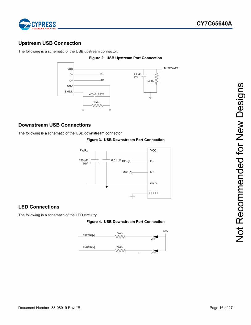
Upstream USB Connection
The following is a schematic of the USB upstream connector.
Figure 2. USB Upstream Port Connection
Downstream USB Connections
The following is a schematic of the USB downstream connector.
Figure 3. USB Downstream Port Connection
LED Connections
The following is a schematic of the LED circuitry.
Figure 4. USB Downstream Port Connection
VCC
D–
D+
SHELL
BUSPOWER
GND
4.7 nF 250V
1 M
D–
D+ 100 k
2.2 F10V
VCC
D–
GND
SHELL
D+
DD–[X]
DD+[X]
PWRx
150 µF10V
0.01 µF
680
680GREEN#[x]
AMBER#[x]
3.3V
Not
Rec
omm
ende
d fo
r New
Des
igns
CY7C65640A
Document Number: 38-08019 Rev. *R Page 17 of 27
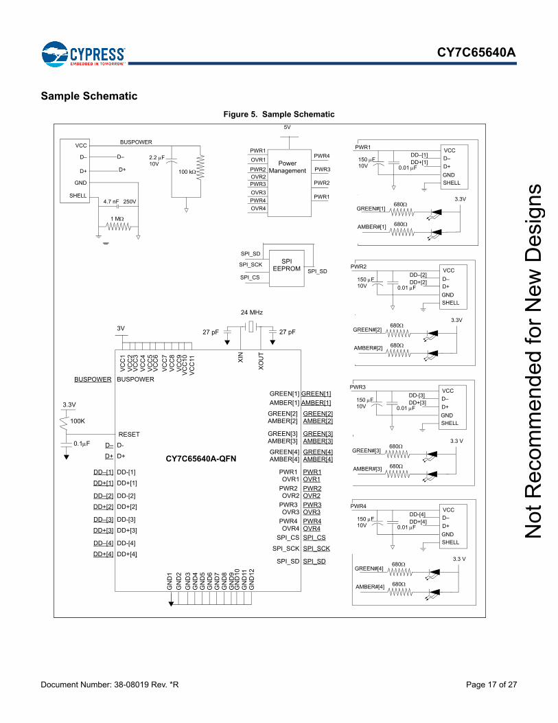
Sample Schematic
Figure 5. Sample Schematic
VCC
D–
D+
SHELL
BUSPOWER
GND
4.7 nF 250V
1 M
D–
D+ 100 k
2.2 F10V
CY7C65640A-QFN
GREEN[1]
AMBER[1]
GREEN[2]AMBER[2]
GREEN[3]AMBER[3]
GREEN[4]AMBER[4]
PWR1OVR1
PWR2OVR2
PWR3OVR3
PWR4OVR4
SPI_CS
SPI_SCK
SPI_SD
DD–[1]
DD+[1]
DD–[2]
DD+[2]
DD–[3]
DD+[3]
DD–[4]
DD+[4]
D–
D+
BUSPOWER
D-
D+
DD-[1]
DD+[1]
DD-[2]
DD+[2]
DD-[3]
DD+[3]
DD-[4]
DD+[4]
GREEN[1]
AMBER[1]
GREEN[2]AMBER[2]
GREEN[3]AMBER[3]
GREEN[4]AMBER[4]
PWR1OVR1
PWR2OVR2
PWR3OVR3
PWR4OVR4
SPI_CS
SPI_SCK
SPI_SD
VC
C1
VC
C2
VC
C3
VC
C4
VC
C5
VC
C6
VC
C7
VC
C8
VC
C9
VC
C1
0V
CC
11 XIN
XO
UT
GN
D1
GN
D2
GN
D3
GN
D4
GN
D5
GN
D6
GN
D7
GN
D8
GN
D9
GN
D1
0G
ND
11G
ND
12
BUSPOWER
RESET
3V
24 MHz
27 pF
0.1F
3.3V
100K
SPIEEPROM
SPI_SD
SPI_SCK
SPI_CS
5V
PWR1
PWR3
PWR4
PowerManagement
PWR1
OVR1
PWR2OVR2
OVR3
PWR3
PWR4
OVR4
VCC
D–
D+
SHELL
GND
150 F
0.01F10V
DD–[1]DD+[1]
PWR1
680
680GREEN#[1]
AMBER#[1]
3.3V
680
680GREEN#[2]
AMBER#[2]
3.3V
VCC
D–D+
SHELL
GND
150 F
0.01F10V
DD–[2]DD+[2]
PWR2
VCC
D–
D+
SHELL
GND
150 F
0.01F10V
DD-[3]DD+[3]
PWR3
680
680GREEN#[3]
AMBER#[3]
3.3 V
680
680GREEN#[4]
AMBER#[4]
3.3 V
VCC
D–
D+
SHELL
GND
150 F
0.01F10V
DD-[4]DD+[4]
PWR4
PWR2
27 pF
SPI_SD
Not
Rec
omm
ende
d fo
r New
Des
igns
CY7C65640A
Document Number: 38-08019 Rev. *R Page 18 of 27
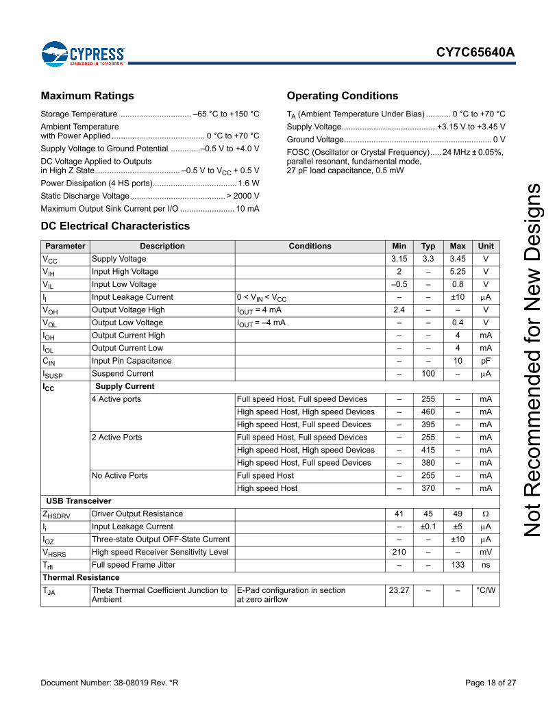
Maximum Ratings
Storage Temperature ............................... –65 °C to +150 °C
Ambient Temperature with Power Applied ......................................... 0 °C to +70 °C
Supply Voltage to Ground Potential .............–0.5 V to +4.0 V
DC Voltage Applied to Outputs in High Z State ..................................... –0.5 V to VCC + 0.5 V
Power Dissipation (4 HS ports)..................................... 1.6 W
Static Discharge Voltage..........................................> 2000 V
Maximum Output Sink Current per I/O ........................ 10 mA
Operating Conditions
TA (Ambient Temperature Under Bias) ........... 0 °C to +70 °C
Supply Voltage..........................................+3.15 V to +3.45 V
Ground Voltage................................................................. 0 V
FOSC (Oscillator or Crystal Frequency)..... 24 MHz ± 0.05%, parallel resonant, fundamental mode, 27 pF load capacitance, 0.5 mW
DC Electrical Characteristics
Parameter Description Conditions Min Typ Max Unit
VCC Supply Voltage 3.15 3.3 3.45 V
VIH Input High Voltage 2 – 5.25 V
VIL Input Low Voltage –0.5 – 0.8 V
Il Input Leakage Current 0 < VIN < VCC – – ±10 A
VOH Output Voltage High IOUT = 4 mA 2.4 – – V
VOL Output Low Voltage IOUT = –4 mA – – 0.4 V
IOH Output Current High – – 4 mA
IOL Output Current Low – – 4 mA
CIN Input Pin Capacitance – – 10 pF
ISUSP Suspend Current – 100 – A
ICC Supply Current
4 Active ports Full speed Host, Full speed Devices – 255 – mA
High speed Host, High speed Devices – 460 – mA
High speed Host, Full speed Devices – 395 – mA
2 Active Ports Full speed Host, Full speed Devices – 255 – mA
High speed Host, High speed Devices – 415 – mA
High speed Host, Full speed Devices – 380 – mA
No Active Ports Full speed Host – 255 – mA
High speed Host – 370 – mA
USB Transceiver
ZHSDRV Driver Output Resistance 41 45 49
Ii Input Leakage Current – ±0.1 ±5 A
IOZ Three-state Output OFF-State Current – – ±10 A
VHSRS High speed Receiver Sensitivity Level 210 – – mV
Trfi Full speed Frame Jitter – – 133 ns
Thermal Resistance
TJA Theta Thermal Coefficient Junction to Ambient
E-Pad configuration in section at zero airflow
23.27 – – °C/W
Not
Rec
omm
ende
d fo
r New
Des
igns
CY7C65640A
Document Number: 38-08019 Rev. *R Page 19 of 27
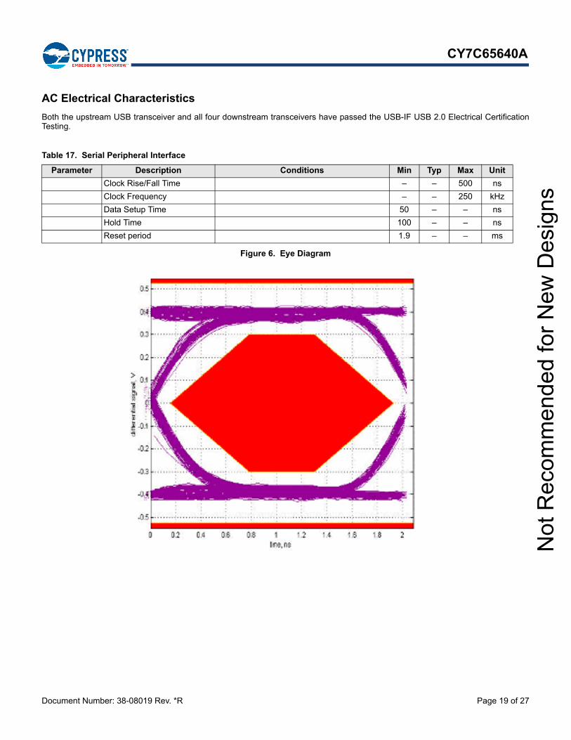
AC Electrical Characteristics
Both the upstream USB transceiver and all four downstream transceivers have passed the USB-IF USB 2.0 Electrical CertificationTesting.
Figure 6. Eye Diagram
Table 17. Serial Peripheral Interface
Parameter Description Conditions Min Typ Max Unit
Clock Rise/Fall Time – – 500 ns
Clock Frequency – – 250 kHz
Data Setup Time 50 – – ns
Hold Time 100 – – ns
Reset period 1.9 – – ms
Not
Rec
omm
ende
d fo
r New
Des
igns
CY7C65640A
Document Number: 38-08019 Rev. *R Page 20 of 27
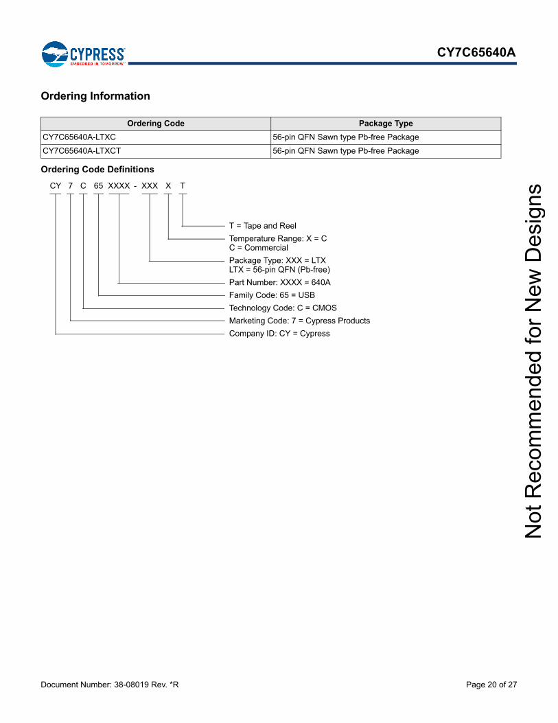
Ordering Information
Ordering Code Definitions
Ordering Code Package Type
CY7C65640A-LTXC 56-pin QFN Sawn type Pb-free Package
CY7C65640A-LTXCT 56-pin QFN Sawn type Pb-free Package
T = Tape and Reel
Temperature Range: X = CC = Commercial
Package Type: XXX = LTXLTX = 56-pin QFN (Pb-free)
Part Number: XXXX = 640A
Family Code: 65 = USB
Technology Code: C = CMOS
Marketing Code: 7 = Cypress Products
Company ID: CY = Cypress
C7 65 XXXX - XXX XCY T
Not
Rec
omm
ende
d fo
r New
Des
igns
CY7C65640A
Document Number: 38-08019 Rev. *R Page 21 of 27
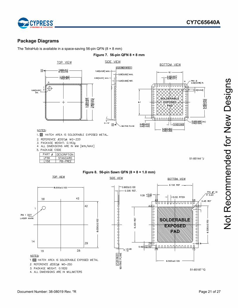
Package Diagrams
The TetraHub is available in a space-saving 56-pin QFN (8 × 8 mm)
Figure 7. 56-pin QFN 8 × 8 mm
Figure 8. 56-pin Sawn QFN (8 × 8 × 1.0 mm)
51-85144 *J
51-85187 *G
Not
Rec
omm
ende
d fo
r New
Des
igns
CY7C65640A
Document Number: 38-08019 Rev. *R Page 22 of 27
Note. The bottom metal pad size varies by product due to diesize variable. If metal pad design or dimension are critical withyour board designs, contact a Cypress Sales office to get thespecific outline option.
Quad Flat Package No Leads (QFN) Package Design Notes
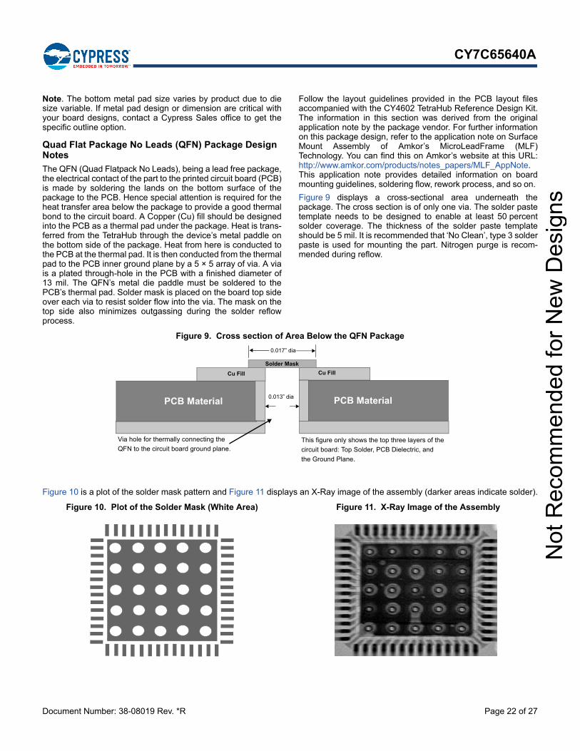
The QFN (Quad Flatpack No Leads), being a lead free package,the electrical contact of the part to the printed circuit board (PCB)is made by soldering the lands on the bottom surface of thepackage to the PCB. Hence special attention is required for theheat transfer area below the package to provide a good thermalbond to the circuit board. A Copper (Cu) fill should be designedinto the PCB as a thermal pad under the package. Heat is trans-ferred from the TetraHub through the device’s metal paddle onthe bottom side of the package. Heat from here is conducted tothe PCB at the thermal pad. It is then conducted from the thermalpad to the PCB inner ground plane by a 5 × 5 array of via. A viais a plated through-hole in the PCB with a finished diameter of13 mil. The QFN’s metal die paddle must be soldered to thePCB’s thermal pad. Solder mask is placed on the board top sideover each via to resist solder flow into the via. The mask on thetop side also minimizes outgassing during the solder reflowprocess.
Follow the layout guidelines provided in the PCB layout filesaccompanied with the CY4602 TetraHub Reference Design Kit.The information in this section was derived from the originalapplication note by the package vendor. For further informationon this package design, refer to the application note on SurfaceMount Assembly of Amkor’s MicroLeadFrame (MLF)Technology. You can find this on Amkor’s website at this URL:http://www.amkor.com/products/notes_papers/MLF_AppNote.This application note provides detailed information on boardmounting guidelines, soldering flow, rework process, and so on.
Figure 9 displays a cross-sectional area underneath thepackage. The cross section is of only one via. The solder pastetemplate needs to be designed to enable at least 50 percentsolder coverage. The thickness of the solder paste templateshould be 5 mil. It is recommended that ‘No Clean’, type 3 solderpaste is used for mounting the part. Nitrogen purge is recom-mended during reflow.
Figure 9. Cross section of Area Below the QFN Package
Figure 10 is a plot of the solder mask pattern and Figure 11 displays an X-Ray image of the assembly (darker areas indicate solder).
Figure 10. Plot of the Solder Mask (White Area) Figure 11. X-Ray Image of the Assembly
0.017” dia
Solder Mask
Cu Fill Cu Fill
PCB MaterialPCB Material0.013” dia
Via hole for thermally connecting the
QFN to the circuit board ground plane.This figure only shows the top three layers of the
circuit board: Top Solder, PCB Dielectric, and
the Ground Plane.
Not
Rec
omm
ende
d fo
r New
Des
igns
CY7C65640A
Document Number: 38-08019 Rev. *R Page 23 of 27
Errata
This section describes the errata for the Tetrahub/CY7C65640A device. Details include errata trigger conditions, availableworkarounds, and silicon revision applicability. Contact your local Cypress Sales Representative if you have further questions.
Part Numbers Affected
MarkingsMarkings for the CY7C65640A consist of:
CY7C65640A-LFXC
YYWW R
Where YYWW is the date code consisting of YY for a two digit year (that is, 2004 is 04) and WW for a work week number within theyear (range is 01 to 52). The chip’s revision letter is represented by the R in the above format.
CY7C65640A Qualification StatusIn Production
CY7C65640A Errata Summary
The following table defines the errata applicable to available CY7C65640A family devices. An "X" indicates that the errata pertains to the selected device.Note Errata titles are hyperlinked. Click on table entry to jump to description.
1. Compliance Testing Setup■ PROBLEM DEFINITION
If downstream ports are not defined contiguously from Port 1 to Port n, the current USB-IF test tool is unable to put TetraHubinto high-speed disconnect test mode.•PARAMETERS AFFECTED
N/A.■ TRIGGER CONDITION
Non contiguous port numbering. For example, physical ports 1, 3, and 4 are used instead of physical ports 1, 2, and 3.■ SCOPE OF IMPACT
The high-speed test patterns cannot be enabled on given ports.■ WORKAROUND
Use contiguous port numbering from port 1 to port n.■ FIX STATUS
Use workaround.
Part Number Device Characteristics
CY7C65640A All Packages
Items CY7C65640A Rev Letter Fix Status
1. Compliance Testing Setup X E Use workaround.
2. D- Driven High on Power Cycling the Hub X E Use workaround.
3. Inter-Packet Delay Timing between LS and FS packet
X E Use workaround.
Not
Rec
omm
ende
d fo
r New
Des
igns
CY7C65640A
Document Number: 38-08019 Rev. *R Page 24 of 27
2. D- Driven High on Power Cycling the Hub■ PROBLEM DEFINITION
When power is cycled on a TetraHub that is already connected to the host and powered (the BUSPOWER pin is in a high state)and configured to operate in high-speed mode (high-speed chirp is not disabled via EEPROM configuration), then TetraHubdrives D- high for about 4.5 ms at the same time that the pull-up resistor on D+ is enabled, resulting in an SE1 state on the busduring this interval. This SE1 state has been observed to cause the part to not complete enumeration on some full-speed hosts.
• PARAMETERS AFFECTEDN/A
■ TRIGGER CONDITION(S)1. TetraHub is configured to operate in high-speed mode (high-speed chirp is not disabled via EEPROM configuration.2. TetraHub is connected to the host and powered (BUSPOWER pin is in a high state)3. Power is cycled on TetraHub.
■ SCOPE OF IMPACTSome full-speed hosts fail to recognize the TetraHub “attach” event and the TetraHub will not enumerate.
■ WORKAROUNDDisconnecting and reconnecting the TetraHub after a power cycle event results in the successful enumeration of the TetraHub.
■ FIX STATUSUse workaround.
3. Inter-Packet Delay Timing Between LS and FS Packet■ PROBLEM DEFINITION
A bus contention situation can occur between TetraHub and a Cypress M8- based full-speed hub, when a full- speed hub (whichuses Cypress’ M8 based full-speed hub silicon) is plugged into TetraHub and both low-speed and full-speed devices areplugged into the downstream ports of the full-speed Cypress hub. This bus contention causes the Cypress full-speed hubrepeater to enter an invalid state, affecting communication to a full-speed device downstream of the full-speed hub.
• PARAMETERS AFFECTEDN/A.
■ TRIGGER CONDITION(S)1. TetraHub is connected to a high-speed host and configured to operate in high-speed mode2. A Cypress M8-based full-speed hub is connected to TetraHub.3. Low and full-speed devices are connected to Cypress M8-based full-speed hub (P/N CY7C650xx, CY7C651xx,
CY7C660xx, and CY7C661xx).4. Full-speed traffic immediately follows low-speed traffic.
■ SCOPE OF IMPACTThis issue has only been observed with full-speed hubs based on Cypress’ M8 based full-speed parts. When the triggerconditions exist and traffic is actively flowing to/from the attached devices, the full-speed device will no longer operate and maydrop off the bus. Note that the problem has not been observed with any other full-speed hub.
■ WORKAROUNDAvoid using a full-speed hub based on an old Cypress M8 based hub part directly downstream of the TetraHub.
■ FIX STATUSUse workaround.
Not
Rec
omm
ende
d fo
r New
Des
igns
CY7C65640A
Document Number: 38-08019 Rev. *R Page 25 of 27
Document History Page
Document Title: CY7C65640A, TetraHub™ High-Speed USB Hub ControllerDocument Number: 38-08019
Revision ECN Orig. of Change
Submission Date Description of Change
** 113506 BHA 04/25/2002 New data sheet (Preliminary)
*A 116812 MON 08/15/2002 Supply voltage range changed from 3.3V–3.6V to 3.15V–3.45Added EPROM types that can be used with HX2 (p. 14)Added description of bit 7 of Byte 12 (Illegal Hub Descriptor) D2 Load (p. 15)Added high speed sensitivity level of receiver (p. 20)Added QFN package design notes (section 16.1)
*B 118518 MON 10/31/2002 Changed status from Preliminary to Final.Fixed the Spec field in the Default Device Descriptor section 7.1Fixed Interface Protocol field of the interface descriptor, section 7.3Fixed Device Protocol field of the interface descriptor, section 7.7Modified table 9-2, section 9.2Added table 9-4, 9-5, section 9.2Added table 4-1, 4-2, section 4.8Added information on bits in wHubCharacterestics, section 7.8Modified figure 16-1 in QFN package design notes, section 16.1Included the eye diagram, section 14.4.2
*C 121793 MON 12/09/2002 Fixed the SPI clock Frequency to 250 KHz, section 14.4.1Added information on the configuration of unused port pins, section 6.0Added statement that no special power up procedure is required, section 6.0
*D 125275 MON 04/02/2003 Changed the name of Bit 3 of Byte 12 of EEPROM for a 0xD2 load (section 8.2) from BusPowered to Reserved.Removed all indication to the misconception that the hub can support bus power.Added information as to which nibble of byte 8 in the EEPROM defines the active ports and which nibble defines the removable ports, section 8.2.Added further information on the BUSPOWER pin (pin 26) functionality in section 6.0.
*E 234272 MON 07/13/2004 Updated Configuration Options:Updated Configured – 0xD2 Load:Updated description (Replaced “CompoundDevice” with “Unused” in the name of Bit 6 of Byte 12.Updated Ordering Information:Updated part numbers.
*F 285171 KKU 11/02/2004 Updated Document Title to read as “CY7C65640A TetraHub™ High-Speed USB Hub Controller”.Replaced CY7C65640 with CY7C65640A in all instances across the document.Updated to new template.
*G 308296 KKU 01/14/2005 Updated Features:Removed “Compound Device”.Updated Default Descriptors:Updated Device Descriptor:Updated Table 4:Replaced “0x0007” with “0x000B” in “Full Speed” and “High Speed” columns corresponding to Byte 12, 13.Updated AC Electrical Characteristics:Updated Table 17:Added “Reset Period” and its details.
*H 390258 KKU 08/03/2005 Updated DC Electrical Characteristics:Added “Thermal Resistance” related information.
Not
Rec
omm
ende
d fo
r New
Des
igns
CY7C65640A
Document Number: 38-08019 Rev. *R Page 26 of 27
*I 522224 TEH 11/15/2006 Updated Pin Definitions:Fixed typo in “Name” column (Replaced [3] with [4] under “DOWNSTREAM PORT 4”). Updated Package Diagrams:spec 51-85144 – Changed revision from *D to *F. Updated to new template.
*J 2657415 DPT / PYRS
02/10/2009 Updated Ordering Information:Updated part numbers.Updated Package Diagrams:spec 51-85144 – Changed revision from *F to *G.Added 51-85187 Rev. *C.
*K 2742387 DPT 07/22/2009 Updated Package Diagrams:spec 51-85187 – Changed revision from *C to *D.
*L 2766203 DPT 09/18/2009 Updated Package Diagrams:No change in revision.spec 51-85187 (Updated for better quality).
*M 2825358 RSKV / PYRS
12/10/2009 Added Contents. Updated Ordering Information:No change in part numbers.Added “Pb-free Package” for Sawn parts in “Package Type” column.
*N 3149016 ODC 01/20/2011 Updated Operating Conditions:Updated details corresponding to “FOSC (Oscillator or Crystal Frequency)”.Updated Ordering Information:Updated part numbers.Added Ordering Code Definitions.Updated to new template.
*O 3404993 AASI 10/13/2011 Added watermark “Not recommended for new designs” across the document.Moved tetrahub (CY7C65640A) to NRND.
*P 4566232 PRJI 11/10/2014 Updated Package Diagrams:spec 51-85187 – Changed revision from *E to *F.Updated to new template.Completing Sunset Review.
*Q 5686754 PRVE 04/06/2017 Updated Package Diagrams:spec 51-85144 – Changed revision from *I to *J.spec 51-85187 – Changed revision from *F to *G.Added Errata.Updated to new template.
*R 5971613 HBM 11/20/2017 Updated Ordering Information:Updated part numbers.Completing Sunset Review.
Document History Page (continued)
Document Title: CY7C65640A, TetraHub™ High-Speed USB Hub ControllerDocument Number: 38-08019
Revision ECN Orig. of Change
Submission Date Description of Change
Not
Rec
omm
ende
d fo
r New
Des
igns
Document Number: 38-08019 Rev. *R Revised November 20, 2017 Page 27 of 27
CY7C65640A
© Cypress Semiconductor Corporation, 2002-2017. This document is the property of Cypress Semiconductor Corporation and its subsidiaries, including Spansion LLC ("Cypress"). This document,including any software or firmware included or referenced in this document ("Software"), is owned by Cypress under the intellectual property laws and treaties of the United States and other countriesworldwide. Cypress reserves all rights under such laws and treaties and does not, except as specifically stated in this paragraph, grant any license under its patents, copyrights, trademarks, or otherintellectual property rights. If the Software is not accompanied by a license agreement and you do not otherwise have a written agreement with Cypress governing the use of the Software, then Cypresshereby grants you a personal, non-exclusive, nontransferable license (without the right to sublicense) (1) under its copyright rights in the Software (a) for Software provided in source code form, tomodify and reproduce the Software solely for use with Cypress hardware products, only internally within your organization, and (b) to distribute the Software in binary code form externally to end users(either directly or indirectly through resellers and distributors), solely for use on Cypress hardware product units, and (2) under those claims of Cypress's patents that are infringed by the Software (asprovided by Cypress, unmodified) to make, use, distribute, and import the Software solely for use with Cypress hardware products. Any other use, reproduction, modification, translation, or compilationof the Software is prohibited.
TO THE EXTENT PERMITTED BY APPLICABLE LAW, CYPRESS MAKES NO WARRANTY OF ANY KIND, EXPRESS OR IMPLIED, WITH REGARD TO THIS DOCUMENT OR ANY SOFTWAREOR ACCOMPANYING HARDWARE, INCLUDING, BUT NOT LIMITED TO, THE IMPLIED WARRANTIES OF MERCHANTABILITY AND FITNESS FOR A PARTICULAR PURPOSE. To the extentpermitted by applicable law, Cypress reserves the right to make changes to this document without further notice. Cypress does not assume any liability arising out of the application or use of anyproduct or circuit described in this document. Any information provided in this document, including any sample design information or programming code, is provided only for reference purposes. It isthe responsibility of the user of this document to properly design, program, and test the functionality and safety of any application made of this information and any resulting product. Cypress productsare not designed, intended, or authorized for use as critical components in systems designed or intended for the operation of weapons, weapons systems, nuclear installations, life-support devices orsystems, other medical devices or systems (including resuscitation equipment and surgical implants), pollution control or hazardous substances management, or other uses where the failure of thedevice or system could cause personal injury, death, or property damage ("Unintended Uses"). A critical component is any component of a device or system whose failure to perform can be reasonablyexpected to cause the failure of the device or system, or to affect its safety or effectiveness. Cypress is not liable, in whole or in part, and you shall and hereby do release Cypress from any claim,damage, or other liability arising from or related to all Unintended Uses of Cypress products. You shall indemnify and hold Cypress harmless from and against all claims, costs, damages, and otherliabilities, including claims for personal injury or death, arising from or related to any Unintended Uses of Cypress products.
Cypress, the Cypress logo, Spansion, the Spansion logo, and combinations thereof, WICED, PSoC, CapSense, EZ-USB, F-RAM, and Traveo are trademarks or registered trademarks of Cypress inthe United States and other countries. For a more complete list of Cypress trademarks, visit cypress.com. Other names and brands may be claimed as property of their respective owners.
Sales, Solutions, and Legal Information
Worldwide Sales and Design Support
Cypress maintains a worldwide network of offices, solution centers, manufacturer’s representatives, and distributors. To find the office closest to you, visit us at Cypress Locations.
Products
ARM® Cortex® Microcontrollers cypress.com/arm
Automotive cypress.com/automotive
Clocks & Buffers cypress.com/clocks
Interface cypress.com/interface
Internet of Things cypress.com/iot
Memory cypress.com/memory
Microcontrollers cypress.com/mcu
PSoC cypress.com/psoc
Power Management ICs cypress.com/pmic
Touch Sensing cypress.com/touch
USB Controllers cypress.com/usb
Wireless Connectivity cypress.com/wireless
PSoC® Solutions
PSoC 1 | PSoC 3 | PSoC 4 | PSoC 5LP | PSoC 6
Cypress Developer Community
Forums | WICED IOT Forums | Projects | Video | Blogs | Training | Components
Technical Support
cypress.com/support
Not
Rec
omm
ende
d fo
r New
Des
igns