Development of ion-implanted optical waveguides in optical materials: A review
20
Development of ion-implanted optical waveguides in optical materials: A review Feng Chen * , Xue-Lin Wang, Ke-Ming Wang School of Physics and Microelectronics, Shandong University, Hong Jia Lou 5, Ji’nan, Shandong 250100, China Received 4 May 2006; received in revised form 25 June 2006; accepted 7 August 2006 Available online 15 September 2006 Abstract As one of most efficient techniques for material-property modification, ion implantation has shown its unique ability for alteration of surface refractive index of a large number of optical materials, forming waveguide structures. The induced refractive index changes are materials related, and closely dependent on the species, energies and doses of the implanted ions. This paper reviews the results of recent research on the fabrication, investigation and applications of the ion-implanted optical waveguides in various optical materials, including crystals and non-crystalline glasses. As will be summarized, ion implantation offers a nearly universal solution for the waveguide fabri- cation in most existing optical materials to date, which opens up new possibilities of attractive optical applications. Ó 2006 Elsevier B.V. All rights reserved. PACS: 42.79.Gn; 61.80.Jh; 42.70.a Keywords: Optical waveguides; Planar waveguides; Channel waveguides; Ion implantation; Nonlinear crystals; Laser crystals; Photorefractive crystals; Waveguide lasers; Waveguide frequency doubling; Two-wave mixing; Waveguide amplifiers 1. Introduction Optical waveguide is one of the basic components in integrated optics and optoelectronics [1–14]. It is character- ized by a region or medium with high refractive index sur- rounded by regions or media with lower index. Such structures allow the confinement of light to regions of the order of light wavelength by means of total internal refrac- tion occurring at the junctions between the boundaries of guides and claddings. Planar or slab waveguides restrict light propagation in one dimension (1D waveguide), whilst channel or ridge waveguides confine the light in two dimen- sions (2D waveguide) [1,2]. The small size of waveguide structures offers high light intensities produced by even very low powers; consequently, the nonlinearities or laser actions in waveguides may be more efficient than those in bulk materials [3]. Moreover, the components based on waveguides may be connected together with optical fibers quite simply because the dimensions of waveguides are directly compatible with fibers used in telecommunications, in which waveguides are often used as amplifiers, signal switches, modulators, etc. [4]. There are several techniques for fabricating waveguides in optical materials, which mainly include diffusion of metal ions [5], ion exchange [6,7], sol gel [8], ion implanta- tion [9] and deposition of epitaxial layers (e.g. sputtering [10], molecular beam epitaxy [11], and pulsed laser deposi- tion [12], chemical vapor deposition [13]). Among these techniques, ion implantation possesses one of the most advantageous characteristics, that is, the wide applicability of materials [14,15]. Since the first proton-implanted wave- guide in fused silica was reported in 1968, waveguides have been so far fabricated in more than 100 optical materials (including crystals, glasses and even polymers) by implan- tation of various ions at the energies of several kilo- electron-volt (keV) up to several mega-electron-volt 0925-3467/$ - see front matter Ó 2006 Elsevier B.V. All rights reserved. doi:10.1016/j.optmat.2006.08.001 * Corresponding author. Tel.: +86 531 8836 4655; fax: +86 531 8856 5167. E-mail address: [email protected] (F. Chen). www.elsevier.com/locate/optmat Optical Materials 29 (2007) 1523–1542
-
Upload
independent -
Category
Documents
-
view
1 -
download
0
Transcript of Development of ion-implanted optical waveguides in optical materials: A review

www.elsevier.com/locate/optmat
Optical Materials 29 (2007) 1523–1542
Development of ion-implanted optical waveguidesin optical materials: A review
Feng Chen *, Xue-Lin Wang, Ke-Ming Wang
School of Physics and Microelectronics, Shandong University, Hong Jia Lou 5, Ji’nan, Shandong 250100, China
Received 4 May 2006; received in revised form 25 June 2006; accepted 7 August 2006Available online 15 September 2006
Abstract
As one of most efficient techniques for material-property modification, ion implantation has shown its unique ability for alteration ofsurface refractive index of a large number of optical materials, forming waveguide structures. The induced refractive index changes arematerials related, and closely dependent on the species, energies and doses of the implanted ions. This paper reviews the results of recentresearch on the fabrication, investigation and applications of the ion-implanted optical waveguides in various optical materials, includingcrystals and non-crystalline glasses. As will be summarized, ion implantation offers a nearly universal solution for the waveguide fabri-cation in most existing optical materials to date, which opens up new possibilities of attractive optical applications.� 2006 Elsevier B.V. All rights reserved.
PACS: 42.79.Gn; 61.80.Jh; 42.70.�a
Keywords: Optical waveguides; Planar waveguides; Channel waveguides; Ion implantation; Nonlinear crystals; Laser crystals; Photorefractive crystals;Waveguide lasers; Waveguide frequency doubling; Two-wave mixing; Waveguide amplifiers
1. Introduction
Optical waveguide is one of the basic components inintegrated optics and optoelectronics [1–14]. It is character-ized by a region or medium with high refractive index sur-rounded by regions or media with lower index. Suchstructures allow the confinement of light to regions of theorder of light wavelength by means of total internal refrac-tion occurring at the junctions between the boundaries ofguides and claddings. Planar or slab waveguides restrictlight propagation in one dimension (1D waveguide), whilstchannel or ridge waveguides confine the light in two dimen-sions (2D waveguide) [1,2]. The small size of waveguidestructures offers high light intensities produced by evenvery low powers; consequently, the nonlinearities or laseractions in waveguides may be more efficient than those in
0925-3467/$ - see front matter � 2006 Elsevier B.V. All rights reserved.
doi:10.1016/j.optmat.2006.08.001
* Corresponding author. Tel.: +86 531 8836 4655; fax: +86 531 88565167.
E-mail address: [email protected] (F. Chen).
bulk materials [3]. Moreover, the components based onwaveguides may be connected together with optical fibersquite simply because the dimensions of waveguides aredirectly compatible with fibers used in telecommunications,in which waveguides are often used as amplifiers, signalswitches, modulators, etc. [4].
There are several techniques for fabricating waveguidesin optical materials, which mainly include diffusion ofmetal ions [5], ion exchange [6,7], sol gel [8], ion implanta-tion [9] and deposition of epitaxial layers (e.g. sputtering[10], molecular beam epitaxy [11], and pulsed laser deposi-tion [12], chemical vapor deposition [13]). Among thesetechniques, ion implantation possesses one of the mostadvantageous characteristics, that is, the wide applicabilityof materials [14,15]. Since the first proton-implanted wave-guide in fused silica was reported in 1968, waveguides havebeen so far fabricated in more than 100 optical materials(including crystals, glasses and even polymers) by implan-tation of various ions at the energies of several kilo-electron-volt (keV) up to several mega-electron-volt

1524 F. Chen et al. / Optical Materials 29 (2007) 1523–1542
(MeV) [14–20]. Although the related topics have been stud-ied for more than 30 years, there is no a unique explanationfor all materials, because of the diversity of configurationand properties, although there are some typical responseswhere we do understand the processes. However, there isone simple model, which was firstly raised by Townsendin 1976 as a prediction [21], that seems to be a reasonableexplanation at least for most crystals. When implantationof light ions at energies of several MeV are performed, amajority of the lattice damage occurs at the end of theion track inside the substrates, which results in a decreaseof physical density by means of volume expansion andhence a reduced refractive index of an optical barrier. Sucha barrier confines the light in a narrow layer with relativelyhigh refractive index between itself and the crystal surface,
Fig. 1. (a) Refractive index profile for a BiB3O6 (BIBO) waveguide formedcomparison, the nuclear energy loss as a function of the penetration depth (vrefractive index profile of a Nd:YVO4 waveguide produced by 3.0 MeV Si+ ion(dashed line) annealing treatment at 240 �C for 60 min.
forming an optical waveguide [14]. If the barrier is not ade-quate high or wide, the so-called tunneling effect may takeplace, accompanying leakage of light energy [22,23]. Fig. 1ashows a typical barrier-type refractive index profile, whichis for a BiB3O6 waveguide formed by 2.8 MeV He+ ionimplantation at the dose of 2 · 1016 ions/cm2. Moreover,one should note that for the waveguides in some crystals,some indices of refraction might first experience a positivechange in the main region of the ion range, forming anenhanced index well, which restricts the guided light in anon-tunneling way [24–26]. Fig. 1b shows the ordinaryrefractive index profile of a Nd:YVO4 waveguide, whichis produced by 3.0 MeV Si+ ion implantation at the doseof 1 · 1015 ions/cm2. Such a model seems to be also appli-cable to the formation of waveguides in some non-crystal-
by 2.8 MeV He+ ion implantation at the dose of 2 · 1016 ions/cm2. Foracancy distribution) in the crystal is also represented [153]; (b) ordinaryimplantation at the dose of 1 · 1015 ions/cm2 before (solid line) and after

Fig. 2. Schematic for single-energy implantation into KNbO3 crystal oftrapezoidal channel waveguides by direct use of a photoresist mask withwedged edges (data obtained from Ref. [39]).
F. Chen et al. / Optical Materials 29 (2007) 1523–1542 1525
line glasses although no ‘‘lattice’’ damage exists in thosematerials [27,28]. Nevertheless, for glasses, the origin ofthe waveguide formation is more complicated to a certainextent because even the same type glasses have differentchemical compositions.
Ion-implanted waveguides in insulating optical materi-als were outlined in an earlier book by Townsend et al., giv-ing a comprehensive summary of the work that had beendone until 1993 [14]. A few short discussions on the associ-ated topics were presented later by Townsend [9] andBuchal [15]. However, as this is a highly active area ofresearch, a number of new and interesting results have beenpublished in the latest years. In the paper, the more recentresults (obtained mainly after 1993; for those obtainedbefore 1993, see Ref. [14] for details) of the work on thefabrication, investigation and applications of the ion-implanted waveguides in optical materials, including crys-tals and non-crystalline glasses, are reviewed in the follow-ing three sections, respectively. Detailedly, in Section 2several common used fabrication and investigation meth-ods for ion-implanted waveguides are introduced briefly;Section 3 describes the recent results of optical waveguidesin various optical materials formed by ion implantationand their properties; in Section 4 a few applications relatedion-implanted waveguides in optical area are given asexamples.
2. Fabrication and investigation methods
This section describes the basic methods of ion-implanted waveguide fabrication and investigation. Severalimplantation methods, annealing treatments, refractiveindex reconstruction methods, waveguide coupling tech-niques and loss measurement methods will be discussed.
2.1. Ion implantation processing
Ion implantation is a mature technology for semicon-ductor production, and has been widely used in the opticalcommunication devices [29,30]. In the research area of theion-implanted waveguides, accelerators are more oftenused because they offer high energies of specific implantedions at acceptable doses [14]. The implanted ions, normallywith positive charges, are extracted out from the sources,experiencing acceleration and mass/energy selection, andbombarded into the target materials by beam scanningtechnique, by which uniform irradiation is ensured overthe sample surface. This method has been adopted forwaveguide fabrication in a large number of optical materi-als. An improved method, a so-called focused ion beam(FIB) implantation, could provide an ion beam with diam-eters ranging from several microns to 100 nm or even muchless, which provides directly selective implantation toregions with small dimensions, forming directly writingwaveguides [31–33]. Since the detailed demonstration ofaccelerators and ion implantation technique could befound in many books and papers [14,34–38], here we con-
centrate on the applications of ion implantation on the for-mation of optical waveguides.
The ion-implanted waveguides may have refractiveindex profiles of optical barrier or non-tunneling well type,or both [14]. The planar waveguides may be fabricated bydirectly ion implantation into the sample, in which case nospecific masks are required because 1D waveguide onlyneeds entire implantation of the target surface. However,for 2D waveguide formation, several other techniques areneeded to construct a mask, assisting to perform selectiveimplantation. In the earlier works, masks were made byfirst depositing a thin photoresist or metal (e.g. Au), andusing standard photolithography technique, finally form-ing negative or positive metal stripes as protective layeraccording to the waveguide type, i.e. either in the optical-barrier or enhanced-well case [14]. Not to lose the general-ity, implantation of He+ ions is discussed here as an exam-ple. If the implantation creates barrier-type waveguides, thecommon way is that, before the mask deposition, the sub-strate is first implanted with high energetic He+ ions (e.g.2.0 MeV) to form an optical barrier at the end of ion track;afterwards the mask with designed stripe structures isdeposited on the surface of the substrate, performing a ser-ies of successive low energy He+ (e.g. 0.3–1.7 MeV) to buildup index-decreased sidewalls, and then the waveguides areformed in the mask-protected regions. These guides areconfined by the barriers and sidewalls together. On theother hand, if the implantation induces index increases ofirradiated regions, theoretically only one implantationstage is needed, in which cases some regions are protectedby the mask while the open stripes are irradiated to formchannel waveguide structures. Recently, it was reportedthat even for barrier-type waveguides one implantationwas enough by using some thick commercial photoresiststripes with wedged edges in the cross-section, formingwaveguides also with wedged cross-sections. In this case,the channel waveguides were confined by a semi-closedbarrier ‘‘wall’’ with lower indices, i.e. the wall was closedinside the material while open to the air at the interfaceof air/waveguide (see Fig. 2) [39]. Alternatively, a specialsetup was lately designed for channel waveguide forma-tion by Moretti et al. In this system, the sample was

1526 F. Chen et al. / Optical Materials 29 (2007) 1523–1542
fixed on a rotatable target holder, irradiated through amovable metal slit. By varying the angle of incident beamwith sample surface continuously, the implantations ofions could create a closed barrier wall or increased-indexwell inside the substrate, hence forming channel wave-guides, see Ref. [40] for details. Furthermore, ridge wave-guides could be fabricated by first implantation and thefollowing selective etching [41,42]. Moreover, the focusedion beam implantation has been used to fabricate directlywriting channel waveguides in optical materials because itoffers the possibility of selective implantation on the sub-strate surface and induce refractive index changes of spe-cific region [43–45].
2.2. Annealing treatment
Since the implantation creates color centers (opticalabsorption sites) by electronic energy deposition, anddestroys somehow the equilibrium of the origin structuresby nuclear collisions, which both inevitably increase thewaveguide losses, therefore annealing treatment is com-monly necessary for all the ion-implanted waveguides incrystals as well as glasses [14]. The aim of anneals is toremove the unwanted defects within the guide region tomaximally preserve the electro-optic or non-linear opticproperties. The methods of annealing treatment so farinclude conventional furnace anneals [46], rapid thermalanneals [47] and laser beam processing [48]. Dependingon the substrate properties, thermal treatment at 200–500 �C are often performed in furnaces for tens of minutesto several hours to be one of effective methods, which insome cases, may reduce the propagation losses of the wave-guides to be as low as �0.1 dB/cm. Moreover, the rapidthermal annealing may abolish the induced defects whileavoid unwanted diffusion simultaneously [47]. Recently,laser beam processing was found to be potentially benefi-cial [9]. By using strongly absorbed radiation, laser energymay be confined to the surface layer to realize local heat-ing, which may remove intrinsic defects and induce crystal-line re-growth or solid phase epitaxy [48,49].
2.3. Refractive index profiles
Since refractive index profiles in the waveguides, withtypical dimensions of several microns can hardly deter-mined by direct measurement, therefore reconstructiontechniques are developed by using effective refractive index(neff) method. One is the inversed Wentzel–Kramer–Brill-ouin (iWKB) method [50–53], and the other is reflectivitycalculation method (RCM), which was developed by Chan-dler and Lama [14,54]. Both of them require first measure-ment of neff, commonly by prism coupling method (m-linespectroscopy) [55–58]. Particularly, for ion-implantedwaveguides, it has been demonstrated that RCM can beuse to reconstruct the refractive index profiles quite well[14]. The first step of this method is to assume a conceivableprofile that is characterized by a set of parameters, and
then by adjusting certain parameters, the calculated profile,with computed neff, may match the measured ones best.With these optimized parameters, such profile is supposedto approximately depict the refractive index behaviors inthe waveguides.
2.4. Waveguide coupling methods
For the measurement of waveguides, the basic investiga-tion is to couple the light into and out of the waveguides,and measure the neff of the guided modes. The commonlyused methods are prism coupling [55–58] and end-fire cou-pling [59–63]. In the former case, the prisms act as modesconverters capable of transferring energy of light betweenguided and radiations modes. When specific conditionsare satisfied, dark lines (dark mode spectroscopy) may beobserved at a set of discrete angles; together consideringthe prism refractive index and figure, the neff of the guidedmodes could be calculated. More recently, an improvedmethod was developed for a non-destructive measurementof ion-implanted waveguides by Guarino et al. The methodwas based on frustrated total internal reflection in a layeradjacent to the waveguide but did not require applied pres-sure, by which the surface of the samples could be free ofany damage induced by the prism-sample extrusion [64].Alternatively, end-fire coupling technique is practically use-ful in integrated optics and optical fiber communications.In this case, light beam, either focused by microscopiclenses or directly output from a fiber, is fed onto the endfacet of waveguides to excite guided wave propagation. Ifthe optical field of the input light matches the mode fields,high coupling efficiency may be obtained [14].
2.5. Waveguide loss measurement
Waveguide propagation loss could be measured basedon the coupling techniques. For ion-implanted waveguides,the attenuation is mainly caused by absorption (ion beamprocessing induced color centers), scattering (determinedby interface roughness) and leakage through the opticalbarriers by tunneling effect (if the waveguides are mainlyconfined with index-decreased barriers). Several methodshave been used to perform waveguide loss measurementfor ion-implanted waveguides, including prism-slidingmethods [65–67], scattering detection techniques [68,69],and Fabry–Perot resonance methods [70,71]. Remarkably,an improved arrangement by using self-pumped phase con-jugation was also achieved to obtain results with goodselection of specific modes, better accuracy or less destruc-tion [72]. In addition, an estimation of waveguide losscould be performed by directly measuring the input andoutput light power through the waveguides and correctedunder reasonable assumptions, i.e. considering the launch-ing coupling efficiency, Fresnel reflections at the input air/waveguide interface, absorption of bulk materials, etc. [39].All the above techniques have been performed for the char-acterization of ion-implanted waveguides.

F. Chen et al. / Optical Materials 29 (2007) 1523–1542 1527
3. Materials
In this section, the fabrication and properties of ion-implanted waveguides in different materials, includingnon-linear crystals, laser crystals and glasses, will bediscussed.
3.1. Non-linear crystals
The non-linear crystals usually have large non-linearoptical coefficients, which could be used for second-har-monic generation (SHG), optical parametric oscillators(OPO) and amplifiers (OPA), and so on [73,74]. In this sub-section, waveguides in several important non-linear crystalswill be discussed.
3.1.1. Lithium niobate (LiNbO3)
Among all the electro-optical materials, LiNbO3 hasbeen studied most extensively because of its combinationof various excellent properties and low costs [75]. Severalmethods have been performed to fabricate and investigateoptical waveguides in LiNbO3, including metal diffusion[5,76], proton exchange [77,78] and ion implantation[22,69,79–103]. So far LiNbO3 waveguides formed by theimplantation of various ions, including H, He, B, C, N,O, F, Si, P, Ti, Cu, Ni, and Ag, with different electrova-lence, energies or doses, have been studied.
Among the many new results that have been obtained,the majority was focused on the fabrication and refractiveindex characterization of the LiNbO3 waveguides byimplantation of ions at low dose (�1014 ions/cm2)[22,69,84,89,90,92–94]. For the He+-implanted LiNbO3
waveguides at high doses (�1016 ions/cm2), the ordinaryrefractive index (no) had a typical barrier-type profile,whilst the extraordinary refractive index (ne) had a morecomplex changes: at surface region ne was increased, butthe maximum positive change was found to be peaked deepinside the guide, resulting in so-called ‘‘missing modes’’;and index-decreased barrier was located at the end of iontrack [82]. The optical barrier, together with the positiveindex well, confined the light propagation in the guide.When single-energy He+ implantation was performed atlow dose, the ne had an index-increased ‘‘wall’’ at the endof the ion range, instead of an index-decreased barrier[84]. Different results were obtained for multi-energy He+
implanted LiNbO3 waveguide at low doses, in which a bur-ied guided mode was found deep inside the waveguide [84].For the implantations of other ions at low doses, e.g. B, C,O, Si, and P, the ne was found to have similar behaviors inthe guide regions [22,69,89,90,92,93].
Based on the experimental results, several hypotheses ormodels were applied to explain the refractive index behav-iors induced by the implantations. A simple mechanismwas, for high birefringent crystals (for LiNbO3,Dn = 0.08), low-dose implantation may induce a positivechange of the lower index (for LiNbO3, ne) while decrease
the higher one (for LiNbO3, no) [84]. Further investigationof the index behaviors may be concentrated on the elec-tronic and nuclear damages, which was inevitably createdby the interactions between the implanted ions and the sub-strate lattices [92]. In some cases, it seems to be reasonablethat electronic energy deposition causes positive indexchanges in terms of Li diffusion or lattice relaxation[14,82]. More recently, planar waveguides formed by 20and 22 MeV F ion implanted into LiNbO3 are believedto mainly due to the electronic excitation, forming a step-like index profile, rather than nuclear damage that resultsin typical barrier-type waveguides [95]. Moreover, Huet al. developed a simple model by combine spontaneouspolarization decrease and the ne increase induced by theimplantation of multi-energy Cu+ ions, which was also fea-sible to explain the existence of missing modes of He+-implanted LiNbO3 waveguides [98]. More recently, Bentiniet al. reported the structural and compositional character-istics of O or C ion-implanted LiNbO3 waveguides, andconcluded that the development of tensile strain inducedby the ion implantation may contribute to the decrease ofthe ordinary refractive index variation through thephoto-elastic effect [102].
The extraordinary refractive index behaviors make itpossible for the formation of 2D waveguides by using sin-gle implantation, combined with lithography technique or/and etching method. For example, using photoresist maskstripes to protect some regions of LiNbO3 surface from theirradiation, allowing some open stripes being implanted,channel waveguides could be formed. For instance, Luet al. reported the two-mode channel waveguide in LiNbO3
by multiple-energy O+ ion implantation, which operates atwavelength of 1.55 lm [94].
The ion implantation into LiNbO3 will cause defectseven destroy the original lattices at high doses [14]. Theunwanted damage may influence the quality of the wave-guides and must be removed to the greatest extent. It wasproved that, in the implanted region of LiNbO3 that,low-dose implantation generates restorable lattice disor-ders, which could be re-crystallized by the annealing atmoderate temperatures [69,79,92,93,97]. Fig. 3 illustratesthe aligned and random spectra of 2.8 MeV P+ ion-implanted LiNbO3 at dose of 1 · 1014 ions/cm2 beforeand after annealing at 200 �C for 30 min, from which onecan see that after moderate annealing the lattice ofimplanted region could recover, compatible to the originalcase. For O3+-implanted LiNbO3 at doses more than4 · 1014 ions/cm2, it seems difficult to remove the latticedefects only be annealing at moderate temperature [92].When proton ion implantation is used, for relatively highdose of 1 · 1016 ions/cm2, the structure of the implantedregion could recover to approximate original lattice [79].In fact, for H+ ion irradiation at even much higher doses(up to 2 · 1017 ions/cm2), only point nature defects areinduced [104], while He+ ion implantation generateslarge-dimension clusters of different crystalline nature
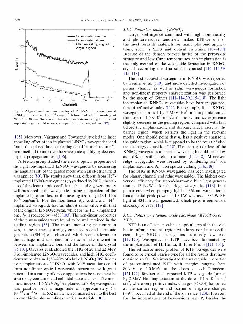
Fig. 3. Aligned and random spectra of 2.8 MeV P+ ion-implantedLiNbO3 at dose of 1 · 1014 ions/cm2 before and after annealing at200 �C for 30 min. One can see that after moderate annealing the lattice ofimplanted region could recover, compatible to the original case [97].
1528 F. Chen et al. / Optical Materials 29 (2007) 1523–1542
[105]. Moreover, Vazquez and Townsend studied the laserannealing effect of ion-implanted LiNbO3 waveguides, andfound that plused laser annealing could be used as an effi-cient method to improve the waveguide quality by decreas-ing the propagation loss [106].
A French group studied the electro-optical properties ofthe light ion-implanted LiNbO3 waveguides by measuringthe angular shift of the guided mode when an electrical fieldwas applied [80]. The results show that, different from He+-implanted LiNbO3 waveguides (r13 reduced by 20%), the val-ues of the electro-optic coefficients (r13 and r33) were prettywell-preserved in the waveguides, being independent of theimplanted-proton dose in the investigated range (�1–10 ·1016 ions/cm2). For the non-linear d33 coefficients, H+-implanted waveguide had an almost same value with thatof the original LiNbO3 crystal, while for the He+-implantedone, d33 is reduced by�48% [103]. The non-linear propertiesof those waveguides were found to be well retained in theguiding region [85]. The more interesting phenomenonwas, in the barrier, a strongly enhanced second-harmonicgeneration (SHG) was observed, which seems relevant tothe damage and disorders in virtue of the interactionbetween the implanted ions and the lattice of the crystal[85,103]. Olivares et al. studied the SHG of 20 and 22 MeVF ion-implanted LiNbO3 waveguides, and high SHG coeffi-cients were obtained (50–80% of a bulk LiNbO3) [95]. More-over, implantation of LiNbO3 with MeV metal ions couldform non-linear optical waveguide structures with greatpotential in a variety of device applications because the sub-strate may contain metal colloidal nano-clusters. The non-linear index of 1.5 MeV Ag+-implanted LiNbO3 waveguideswas positive with a magnitude of approximately 5 ·10�10 cm�2 W�1 at 532 nm, which compared well to the bestknown third-order non-linear optical materials [101].
3.1.2. Potassium niobate (KNbO3)
Large birefringence combined with high non-linearityand photorefractive sensitivity makes KNbO3 one ofthe most versatile materials for many photonic applica-tions, such as SHG and optical switching [107–109].Because of the densely packed lattice of the perovskitestructure and low Curie temperatures, ion implantation isthe only method of the waveguide formation in KNbO3
crystal, according the data so far reported [110–114,39,115–118].
The first successful waveguide in KNbO3 was reportedby Bremer et al. [110], and more detailed investigation ofplanar, channel as well as ridge waveguides formationand non-linear property characterization was performedby the group of Gunter [111–114,39,115–118]. The lightion-implanted KNbO3 waveguides have barrier-type pro-files of refractive index [111]. For example, for a KNbO3
waveguides formed by 2 MeV He+ ion implantation atthe dose of 1.5 · 1015 ions/cm2, the na and nb experienceslightly decrease in the guiding region, compared with thatbefore the implantation, and decrease much more at thebarrier region, which restricts the light in the relevantmodes. One should point that nc has a positive change inthe guide region, which is supposed to be the result of elec-tronic energy deposition [118]. The propagation loss of theKNbO3 waveguides at specific wavelength could be as lowas 1 dB/cm with careful treatment [114,118]. Moreover,ridge waveguides were formed by combining He+ ionimplantation and Ar+ ion sputter etching [116,118].
The SHG in KNbO3 waveguides has been investigatedfor planar, channel and ridge waveguides. The highest con-version efficiency for second-harmonic blue light genera-tion is 12.1% W�1 for the ridge waveguides [116]. In aplanar case, when pumping light at 868 nm with internalfundamental peak power of 1.3 kW was used, 385 W SHlight at 434 nm was generated, which gives a conversionefficiency of 29% [118].
3.1.3. Potassium titanium oxide phosphate (KTiOPO4 or
KTP)
KTP is an efficient non-linear optical crystal in the visi-ble to infrared spectral region with large non-linear coeffi-cient, high SHG efficiency, and relatively low cost[119,120]. Waveguides in KTP have been fabricated bythe implantation of H, He, Li, B, F, or P ions [121–131].
The refractive index profiles of KTP waveguides werefound to be typical barrier-type for all the results that haveobtained so far. We investigated the waveguide propertiesof proton-implanted KTP with energies ranging from80 keV to 1.0 MeV at the doses of �1016 ions/cm2
[121,122]. Bindner et al. reported KTP waveguide formedby 2 MeV He+ implantation at the dose of 1 · 1016 ions/cm2, where very positive index changes (<0.5%) happenedat the surface region and barrier of negative changes(�9%) occurred at the end of the ion range [123]. However,for the implantation of heavier-ions, e.g. P, besides the

F. Chen et al. / Optical Materials 29 (2007) 1523–1542 1529
barrier, large index decrease was found at the surfaceregion as well [130].
The lattice structures experience damages to somedegree, and may be recover somehow by heat treatmentat moderate temperatures. Opfermann et al. studied theradiation effects of MeV He+, Li+ and B+ ion implantationinto KTP by cross-sectional transmission electron micros-copy (XTEM) [126]. The results show that, for He or Liimplantation at high doses, buried amorphous layer, actingas optical barrier, are located at the region where mostnuclear damage happens; between the barrier and the sur-face, almost perfect KTP crystalline layer, which acts as awaveguide. For B+ ion-implanted waveguides, even at verylow doses of 5 · 1013 ions/cm2, a significant contribution ofdamage is caused by electronic energy deposition, resultingin defects in the guide region [126]. Recently, Schrempelet al. reported buried channel waveguides in KTP by multi-ple He ion implantation with the combination of maskingtechnique or/and ion exchange [128]. Fig. 4 shows the sche-matic of the fabrication process. The propagation losses of6–9 dB/cm were obtained after thermal annealing treat-ment up to 500 �C. The optimization of the fabricationconditions and the post-implantation annealing may behelpful to reduce the attenuation value for practical opticalapplication.
The SHG was reported in He+-implanted KTP wave-guides with conversion efficiency of 25% for incident pulsesof 1 lJ and length of 20 ns [124]. The most advantageous offrequency doubling of such waveguide was, when small sig-
Fig. 4. Schematic of the fabrication processing by producing surroundingareas with decreased refractive index in KTiOPO4 by ion irradiation (dataobtained from Ref. [128]).
nal excitation was used, the second-harmonic efficiencycould be much higher than that of the bulk material[3,14]. The non-linear properties of multi-energy He+
implanted KTP waveguide was measured by Kremeret al., using second-harmonic wave generated with evanes-cent wave (SHEW) method, and the non-linear coefficientd33 of the waveguide was found to be �50% of the un-irra-diated bulk crystal [131]. Therefore, the frequency doublingefficiency of ion-implanted KTP waveguides was a combi-nation of waveguide enhancement and implantation-induced degradation of non-linearities.
3.1.4. Lithium triborate (LiB3O5 or LBO)
As one of important crystals in so-called borate family,LBO is unique in many aspects, especially its wide trans-parency range (particularly in UV range), moderately highnon-linear coupling, high damage threshold and goodchemical and mechanical properties [132]. The conven-tional method, for waveguide fabrication such as metal dif-fusion and ion exchange, is not feasible for LBO. So far,only He+-ion-implanted LBO waveguides have beenreported [133–136].
The reconstructed refractive index profiles show thatLBO planar waveguides have typical barrier-type shapes[133–136]. The multi-energy He+ implantation has beenused for formation of either thicker barriers [134] or doublelayer guides [135]. Davis et al. reported the channel wave-guides in LBO, which were formed by multiple He+ ionimplantation with a 10- and 17-lm-diam gold mask toform sidewalls of channels followed by implantation with-out the mask to define the barrier [134]. The SHG conver-sion efficiency of 7 · 10�5% was achieved for the LBOchannel waveguide at pump light wavelength of 937 nmand power of 9.6 mW. The reason for this low value wasattributed to the very low pumping power density andthe multi-mode structures of the waveguide. Even though,such conversion efficiency was still comparable to that ofsame power pumped bulk crystal [134]. Moreover, Bak-houya et al. investigated the SHG for a LBO planar wave-guide formed by double energy He+ ion implantation attotal dose of 3.9 · 1016 ions/cm2, and obtain 10–4 cm�2 W�1 at 923 nm with pump power of 250 mW [136].
3.1.5. Gadolinium calcium oxoborate (Ca4GdO(BO3)3 or
GdCOB)
GdCOB is one of most interesting crystals for frequencydoubling of diode infrared light to achieve visible lasers.The good mechanical properties and wide transmissionrange makes it as an ideal medium for a combination ofIR laser with SHG to realize possible self-frequency con-version [137]. The bulk crystal may have a conversion effi-ciency of 50% at 1064 nm with the excitation of pulsed laser[138]. As yet it seems that the ion implantation is the onlymethod for the waveguide formation in this crystal [139–142].
Boudrioua et al. reported the formation of both planarand channel waveguides in GdCOB by MeV He+ ion

1530 F. Chen et al. / Optical Materials 29 (2007) 1523–1542
implantation [139,140]. The refractive index profiles of thewaveguides are of typical barrier shape [139,141]. For asingle-energy implanted waveguide, an efficient guidinglayer requires high-dose implantation (higher than 2 ·1016 ions/cm2), and the propagation loss could be �5 dB/cm. It was proved that multiple-energy implantations areusually helpful to reduce the losses by widening the barrierand hence minimizing the tunneling effect. The opticallosses for triple-energy He+ implanted GdCOB waveguidescould be of the order of 2 dB/cm [139].
The SHG of the planar waveguides in GdCOB wasachieved at the pumping laser excitation at wavelength of823 and 960 nm for an arrangement of Type I phase match-ing [142]. The conversion efficiency of 10�2 was obtainedfor the as-implanted planar waveguides for the fundamen-tal TM mode to first-harmonic TE mode at pumping powerof 250 mW. The SHG efficiency could be improved by opti-mizing the fabrication and post-implantation process (e.g.annealing treatment) of the planar waveguides, which isexpected to be 10%, or using a channel waveguide[140,142]. In the latter case, at pumping wavelength of810 nm at 250 mW, frequency conversion in channels hasrealized with an efficiency of 20% higher than that in theplanar waveguides [142].
3.1.6. b-Barium borate (b-BBO)
b-BBO is a promising non-linear crystal, which com-bines wide transparency range, large non-linear coeffi-cients, wide thermal acceptance bandwidth and highdamage threshold [143]. Like most of the crystals, it is dif-ficult to use conventional techniques to form waveguidestructures in b-BBO. Up to now, planar waveguides in b-BBO have been fabricated by using MeV He+, O+ or Si+
ion implantations [136,144–146].In the He+ implanted cases, the waveguides are found to
have a barrier-type shape. Both no and ne have an index-decreased barrier; however, in the guide region, no
decreases slightly while ne has a small positive change evenfor high dose of 2 · 1016 ions/cm2 [136,144]. Differently, inthe case of O+ implanted waveguides at very low doses (5–500 · 1012 ions/cm2), the ne exhibits large increase, formingnon-tunneling waveguide structures by the induced index-increased well [145]. Since the ion dose could be verylow, the induced damage by the implantation is expectedto be enough small, and the non-linear properties couldbe well preserved. The measured propagation loss of theO+ implanted waveguide was �1.6 dB/cm for an as-implanted sample [145], which exhibits the potential forits applications in photonic area. The refractive index pro-files of Si+ ion-implanted b-BBO waveguides were found tobe similar to those of O+ implanted one [146].
3.1.7. Other non-linear materials
Ion implantation has been used to form optical wave-guides in a few other non-linear crystals, including LiTaO3
[147–149], Li2B4O7 (LTB) [136,150], Bi4Ge3O12 (BGO)[151,152], BiB3O6 (BIBO) [153,154], KTiOAsO4 (KTA)
[25,155,156], Ca4YO(BO3)3 (YCOB) [157,158], etc. It isfound that among these materials, the implantations ofhigh-dose light ions creates typical barrier-confined wave-guides, while in the cases of low-dose heavier-ion implanta-tion, index-increased well may be responsible for theformation of BIBO and KTA waveguides [153,156].
3.2. Photorefractive crystals
Crystals with photorefractive properties have attractedmore attention because they offer the possibility for refrac-tive index modulation and hence the potential applicationin holographic storage and optical communications[159,160]. In addition to LiNbO3 or LiTaO3, some of theother photorefractive crystals have their respective physicalproperties, and hence waveguides in most of them could befabricated by techniques of metal diffusion or ionexchange, which usually requires relatively high tempera-ture treatment. This fact makes ion implantation almostthe unique method for an efficient waveguide formationin these crystals [160].
3.2.1. Strontium barium niobate (SrxBa1-xNb2O6,
0.25 6 x 6 0.75 or SBN)
SBN is a promising photorefractive crystal with largeelectro-optic coefficients. Because of its high-quality opticalproperties, SBN permits many applications in optical datastorage, light modulation, and optical switching [161].Waveguide formation in this crystal can be performed byvirtue of sulphur or zinc in-diffusion [162], static strain-optic effect [163], and ion implantation [164–174].
He+ ion-implanted waveguides in SBN was firstly men-tioned by Youden et al. [164], and for a detailed investiga-tion, Kip et al. reported the refractive index profiles,photorefractive properties and photonic applications (i.e.solitons) of both He and H ion-implanted SBN waveguides[165,166,169–174]. More recently, we reported the wave-guide formation in SBN in one layer as well as double-bar-rier type by means of single or double B ion implantation[167,169].
The refractive index profiles of the SBN waveguidesseem to be optical-barrier-confined. The attenuation coeffi-cients of the He+ ion-implanted SBN waveguides seem tobe very high, of �25 dB/cm, when high-dose implantationof �1016 ions/cm2 was performed [164]. The minimumpropagation loss of the reported SBN waveguides was�1.7 dB/cm, which was measured from a H+-implantedsample at the dose of 4 · 1016 ions/cm2. For the He+ ion-implanted waveguides, losses could be as low as �2 dB/cm when low-dose implantation (�1014–1015 ions/cm2)was performed [165,166].
The two-wave mixing in low-dose He+ ion-implantedCe:SBN61 waveguides shows that the related response timeis decreased by one or two orders of magnitude when com-pared with that of the bulk materials at same intensity. Themeasured maximum two-wave gain coefficient of 45 cm�1
and the response time of a few milliseconds make them

Fig. 6. Erasure times of two-wave mixing of (a) Cu–KNSBN with 2.8-MeV He+ implantation at dose of 1 · 1016 ions/cm2 and (b) Cu–KNSBNwithout ion implantation [184].
F. Chen et al. / Optical Materials 29 (2007) 1523–1542 1531
quite promising candidate for photonic applications [165].However, for H+ ion-implanted SBN waveguide, theconductivity of the sample became much larger, close tometallic one, which makes the measurement of the wave-guide photorefractive properties quite difficult [165]. More-over, solitons formation and mutual interaction inHe+ implanted SBN waveguides have been studied, andall-optical switching based on the solitons is realized[169–174].
3.2.2. Barium titanate (BaTiO3)
BaTiO3 is one of the most promising photorefractivecrystals for its very large electro-optical coefficients ofr131 = 1640 pm/V. It is used as image amplifiers, phase con-junction mirrors, and novelty filters [175,176]. Like some ofthe other crystals, BaTiO3 thin films could be formed byfilm deposition techniques, e.g. pulsed laser deposition[177]. However, ion implantation is still the most efficientmethod for a BaTiO3 waveguide formation [164,178–181].
The first BaTiO3 waveguide was fabricated by Morettiet al. in 1990 by using 2 MeV He+ implantation at the doseof 1016 ions/cm2, and later H+ ion-implanted BaTiO3
waveguide was also reported in 1992. Both the ne and no
have barrier-confined shapes, and the more importantwas that the optical properties of the crystals were foundto be well preserved in the guiding regions.
The two-wave coupling was first achieved for a 1.5 MeVH+-implanted BaTiO3 waveguide at wavelength of 488 and568 nm, by which gain coefficients of 16.5 cm�1 wasobtained [164]. At wavelength of 514.5 nm the highest gainof 58 cm�1 was obtained for a multiple-energy He+
implanted BaTiO3 waveguide [181]. Recently a maximumgain of 24 cm�1 was measured for a He+ ion-implantedRh:BaTiO3 waveguide for infrared light at 854 nm[182,183]. The response time for all of the measurementsin the waveguides was found to be one to three orderslower of magnitude when compared with that of the bulkcrystals at the same power (see Fig. 5) [183].
Fig. 5. Response time t versus the intensity of light inside the BaTiO3
waveguide (filled diamond) and inside the bulk crystal (filled square). Thestraight lines are numerical adjustments of the experimental dataaccording to power laws I2x (data obtained from Ref. [181]).
3.2.3. Other photorefractive crystals
The barrier-confined optical waveguides were alsoreported for some other photorefractive crystals, includingpotassium sodium strontium barium niobate ((K0.5Na0.5)0.2
(SrxBa1�x)0.9Nb2O6 or KNSBN) [184–186], iron dopedlithium niobate (Fe:LiNbO3) [88] and potassium niobate(Fe:KNbO3) [187,188], lead germanate (Pb5Ge3O11 orPGO) [189], KTa1�xNbxO3 [190]. For the He+-implantedCu:KNSBN waveguides, it was found that the erasure timeof the refractive index gratings is longer than that of bulkmaterial, which may mean a better fixing effect of the grat-ings in the waveguide region (see Fig. 6) [184].
3.3. Laser crystals
Crystals doped with laser active ions, such as Nd3+,Er3+, Yb3+, are the most important components of solid-state lasers. So far, the Nd3+ lasers have been operated suc-cessfully in a variety of host crystals, which allow three- orfour-level system laser action [191,192].
3.3.1. Yttrium aluminum garnet (Y3Al5O12, YAG)
YAG is one of a most extensively used laser crystals,and the commercial lasers based on the bulk Nd:YAGare quite mature. Up to now, almost all the high-powerlasers use this crystal as their working medium [193]. Dueto the high chemical stability of YAG, it seems very diffi-cult for optical waveguide formation in this crystal bymeans of metal diffusion or ion exchange techniques.Implantations of proton, He, and C ions have been usedto fabricate waveguides in YAG [40,194–196], and hencerealize the waveguide lasers [197–200].
The earlier reported YAG waveguides were formed byHe+ ion implantation at the dose of �1016 ions/cm2. Therefractive index was increased after the implantation, form-ing an index-enhanced well, which obtained a goodconfinement of the light in the waveguide [195]. RecentlyH+ (at energies of 1–1.25 MeV and doses of 4–6 ·1016 ions/cm2) or C+ (at energy of 7 MeV and dose of1 · 1016 ions/cm2) ion implantation was performed toNd:YAG crystals, by which the planar waveguides werefabricated [194,196]. The channel waveguide in this crystal

1532 F. Chen et al. / Optical Materials 29 (2007) 1523–1542
was reported by H or He ion implantation combined withspecial mechanic masking [40]. To optimize the laseraction, the luminescence properties of the Nd:YAG wave-guides were investigated. It was found that the implanta-tion process does not influence the luminescenceexcitation in the waveguide region, particularly for H+
ion-implanted waveguides [40,49]. Nevertheless, laseractions were achieved for all the H+, He+ and C+ ion-implanted planar Nd:YAG waveguides, respectively, inwhich the pumping threshold power for the laser genera-tion at 1.06 lm was 10–80 mW [197]. More recently, laseraction at 1.34 lm was realized in a proton-implantedNd:YAG waveguide [200].
3.3.2. Neodymium doped yttrium vanadate (Nd:YVO4)
Nd:YVO4 has been growing in popularity because of itshigh gain, low threshold, and high absorption coefficientsat pumping wavelengths, which results from the excellentfit of the Nd3+ dopant in the crystal lattice. These advanta-ges make Nd:YVO4 be a better candidate than Nd:YAGfor low-power devices such as hand-held pointers, and oth-ers compact lasers [201,202]. Up to now, ion implantation,e.g. Si+, Ni+, Cu+, H+, C+, O+ ions, is the only reportedmethod for waveguide formation in Nd:YVO4 crystals[154,203–207].
We reported on the first planar waveguide in Nd:YVO4
crystals by 3.0 MeV Si+ ion implantation at the dose of1 · 1015 ions/cm2 [203]. The induced large positive changeof no (Dno � 0.1) was found to be responsible for the wave-guide formation. The profile of ne in the waveguide was atypical barrier-confined one. The possible reason for thelarge increase of no after the implantation may be a combi-nation of irradiation effects and high birefringence of thesubstrate crystal (ne � no = 0.22). Usually the formerinduces refractive index decrease by nuclear energy deposi-tion, and the latter causes higher index to decrease while
Fig. 7. Near-field intensity distribution of quasi-TM modes measured at the ouimplantation at dose of 1 · 1015 ions/cm2: (a) TM00, (b) TM10 of 4 lm-wide, (260 �C for 30 min, and (e) TM00 of 4 lm-wide waveguide after annealing at 2
the lower one to increase. The no-enhanced waveguideavoids energy leakage, and could be formed in Nd:YVO4
by very low-dose ion implantation (for example,�1 · 1013 Si+/cm2), resulting in slightly lattice damageand low propagation loss (about 1–3 dB/cm) [205]. Thepropagation mode of the waveguide could be managedby using either suitable heat annealing [204] or correspond-ing doses for implantation [205]. The H+ or C+ implantedNd:YVO4 waveguides were also investigated, and the lumi-nescence properties were found to be well preserved in theguide region, which shows potential achievement of wave-guide lasers in Nd:YVO4. More recently, we reported achannel waveguide formation in Nd:YVO4 crystal by com-bination of O+ ion implantation and photoresist masking.At dose of 1 · 1015 O+/cm2, the large no enhanced channels(quasi-TM) are highly multi-mode, however, after suitableannealing, the single-mode waveguide could be formed,with a relatively low loss of �1.7 dB/cm (see Fig. 7) [208].
3.3.3. Rare earth doped- sodium yttrium tungstate
(NaY(WO4)2)
Recently strong attention has been focused on tungstatecrystal materials for their attractive v(2) and v(3) non-linear-ities for second-harmonic generation (SHG) and stimulatedRaman scattering (SRS) [209]. Rare-earth doped tungstatecrystals, such as NaY(WO4)2, are idea candidate hosts forRoman laser generation [210].
The Nd, Er, or Tm doped NaY(WO4)2 waveguides weresuccessfully fabricated by MeV He+ ions at the doses of�1016 ions/cm2 [211,212]. When heavier ions, e.g. P+ orNi+, were used, the doses for waveguide formation inNaY(WO4)2 could be reduced, namely to be �1015 ions/cm2 [212]. It was found that for all the NaY(WO4)2 wave-guides, barrier-type refractive index profiles were recon-structed according to the measured effective refractiveindices of the modes. Compared with He+ ion implanta-
tput facet of the Nd:YVO4 channel waveguides formed by 3.0 MeV O+ ionc) TM20 of 5 lm-wide, (d) TM11 of 6 lm-wide channels after annealing at60 �C for 150 min + 360 �C for 120 min [208].

F. Chen et al. / Optical Materials 29 (2007) 1523–1542 1533
tion, which only induces slight decrease of index in theguide region, one could find that the P+ or Ni+ implanta-tion has a stronger influence on the refractive index, whichcreates relatively large decrease of index not only in thebarriers but also in the guide region. Moreover, the wave-guides formed by heavier-ion implantation seem to becomethicker than the expected value from TRIM simulation[213]. The reason of this may be the radiation enhancedvacancy diffusion, which causes the barrier drift towardsdeeper region inside the crystal. In fact, this phenomenonmay exist for most of the heavier-ion-implanted wave-guides in crystals.
3.3.4. Other laser crystalsPlanar waveguides have been fabricated by ion implan-
tation in many laser crystals, including Nd3+ or Er3+ dopedYAP (Nd:YAlO3, Er:YAlO3) [14,214], GGG(Gd3Ga5O12)[14], Nd:MgO:LiNbO3 [215,216], Ti:sapphire, Nd:BGO,Nd:YSO(Y2SiO5) [14], NdLiP4O12 [217], YSAG(Y3-Sc2Al3O12), GSAG(Gd3Sc2Al3O12), GSGG(Gd3Sc2Ga3O12)[14], Nd:GdVO4, Nd:YbVO4, Nd:LuVO4 [218], Nd:YAB[219], Nd:YCOB (Nd:YCa4O(BO3)3) [158], Yb:GdCOB[141]. Moreover, infrared to green upconversion wasrecently demonstrated in channel waveguides in Er:YAlO3
[214], and buried and channel waveguides were also formedin Ti:sapphire [220]. Among these, waveguide lasers havebeen achieved for the first five crystals.
3.4. Other crystals
Ion implantation has been used to produce waveguidestructures in several other crystals that have special opticalproperties [221–229]. For example, lithium fluoride (LiF),containing color centers, is of great interest for integratedoptics, micro-cavities, and laser applications [230]. Siliconcarbide (SiC), with its wide band-gap and large transpar-ency region, is a good semiconductor candidate for elec-tronic and optical devices [231]. Single crystals of therelaxor ferroelectric lead zinc niobate–lead titanate[(1 � x) · [Pb(Zn1/3Nb2/3)O3]–(x)[PbTiO3] or PZN–PT]exhibits an large piezoelectric response near the morpho-tropic phase boundary, and considerable high electro-opticcoefficients [232]. Silver thiogallate (AgGaS2) has attractedmore attention for the middle and deep infrared (IR) appli-cations due to its large non-linear coefficients and the hightransmission in the IR region [233]. Tin thiohypodiphos-phate (Sn2P2S6) is a wide band-gap semiconductor ferro-electric with large electro-optical coefficients and efficientphotorefractive properties for visible and near-infraredapplications [234].
The channel waveguide in LiF could be fabricated byelectronic beam lithography at the crystal surface [235].Alternatively, the planar LiF waveguides are formed byHe+ ion implantations [221], for example, at energies of1.1–2.0 MeV, and doses of 6 · 1013–2.5 · 1016 ions/cm2
[222]. The waveguides have index-enhanced well in theguide region while index-decreased barrier inside the crys-
tal. Note that high-dose implantation creates large andhigh low-index barrier, whilst low-dose irradiation gener-ates more efficiently the increase of surface index. The elec-tronic and the nuclear energy losses of the incident ionswere suppose to be responsible for the two mechanisms[223]. Moreover, for the 1.1 MeV He implanted LiF, theconcentration of F (250 nm) and F2 (450 nm) color centersis increased gradually when the dose ranges from 1 · 1014
to 2 · 1015 ions/cm2. Low-dose He irradiated LiF wave-guides may have a low propagation loss of �1.5 dB/cm[221]. More recently, channel waveguides in LiF werereported by 1.5 MeV He+ ion implantation combined withmasking technique [224]. The good performance of the LiFwaveguides exhibits potential applications in related fields.
Wesch et al. reported on the first SiC multi-mode wave-guides formed by O implantation at energies of 1.8–3 MeVand doses of 1.6–2.6 · 1017 ions/cm2 at 700 �C [225,226].Such High temperature implantation generates a buriedSiC–SiO2 layer with lower index compared with bulk,which confines the light in the waveguide. The annealingat 1200 �C was performed to the waveguide samples inorder to decrease the induced damage. By combiningfocused ion beam or chemical etching, stripe SiC wave-guides were fabricated.
The planar waveguide in 0.955PZN-0.045PT single crys-tal was formed by 3.8 MeV He+-implantation at the doseof 5 · 1016 ions/cm2 at 58 �C [227]. The refractive indexprofile of the waveguide was typical barrier type. Afterthe rapid thermal annealing the barrier was found tobecome shaper and lower. The high solution X-ray diffrac-tion investigation showed an impact effect of the implanta-tion on the depth dependence of lattice constants in thewaveguide region. The first AgGaS2 waveguide wasformed by a 3.0 MeV Si+ ion implantation at the dose of1 · 1015 ions/cm2 at room temperature. The reconstructedrefractive index profiles showed that the TE modes (ne)were determined by index-enhanced well and index-decreased barrier, while TM modes (no) were only relatedto the barrier [228].
Guarino et al. reported on the first planar waveguideformation in Sn2P2S6 by low-dose (of 0.5–2 · 1015 ions/cm2) He+ ion implantation. The results show that evenfor such low dose, the waveguides are multi-mode. Thewaveguides therefore were considered to be nearly typicalbarrier-confined ones. From the reconstructed refractiveindex profiles, the negative index changes of barriersincreased when higher doses were used, but it reached thethreshold value at dose of �1 · 1015 ions/cm2. The wave-guide loss was determined to be 10 + 2 dB/cm at wave-length of 1.55 lm [229].
3.5. Glasses
Some optical glass materials are particularly suitable tobe the hosts of laser dopants, and hence rare-earth dopedlaser glasses are now commercial available. The commonmethod for waveguide formation in some glasses, e.g.

1534 F. Chen et al. / Optical Materials 29 (2007) 1523–1542
silicates and phosphates, is ion exchange [7,14]. This chem-ical process achieves refractive index increase of the surfaceregion (waveguide) by the exchange of specific ionsbetween the substrate and the ambient chemical liquid.However, the origin of the ion-implanted glass waveguidesis much more complicated [14].
3.5.1. Silicate glasses
Silicate glasses are excellent candidates for waveguideamplifiers and lasers because of their high solubility forrare-earth ions, such as Nd3+, Er3+, and Yb3+, as well asthe chemical robustness. By the exchange of K+/Na+ orAg+/Na+ ions, planar and channel waveguides could befabricated in silicate wafers. Ion implantation is also effec-tive for the modulation of refractive index of silicate glass.However, the silicate is amorphous, particularly with nofixed composition; different silicate may have different ratiofor the same composition.
Earlier work on the ion-implanted waveguides in silicateglasses was done by Kakarantzas et al. in 1992 [236]. Fromtheir results, standard optical barrier-type waveguides wereformed by He+ ion implantation at the doses of�1016 ions/cm2. A considerable large index decrease hap-pened in the surface region, which degraded the waveguidequality [27]. Because silicate is a mixture, refractive indexbehaviors may be different from other silicate glasses. Wereported on optical waveguide formation in one silicateglass, which exhibited index increase in the surface region,resulting in non-tunneling waveguide structures. Theresults show that, for light ion-implanted silicate wave-guides, a refractive-index-decreased barrier exists at theend of ion range, whilst in heavier-ion-implanted case, nosuch barrier is built up [237].
Waveguides with large index decrease exhibit high prop-agation losses. Even for annealed samples, the loss could be�15 dB/cm, which is too high to be acceptable for practicalapplications [236,27]. However, low loss may be obtainedfor silicate waveguides confined by index-increased wellsdue to the non-leaky properties. We reported on a single-mode Nd-doped silicate waveguide, which was formed by3.0 MeV Si+-ion implantation at low dose of �1014 ions/cm2, with propagation loss of only �0.6 dB/cm afterannealing treatment at 218 �C for 60 min [238]. Foranother silicate waveguide fabricated by 6 MeV carbonion implantation, the losses of the first two modes were0.42 and 0.91 dB/cm after moderate annealing treatments,respectively [239]. Low propagation attenuation suggeststhe potential usage in related fields.
3.5.2. Phosphate glass
Er3+/Yb3+ co-doped phosphate glasses are extensivelyused in the field of telecommunications to form erbium-doped waveguide amplifiers (EDWA). The most commonmethod for waveguide formation in these glasses is ionexchange. Alternatively, implantation of light as well asheavy ions could be used to fabricate waveguides in phos-phate glasses. The earlier work from Kakarantzas et al.
showed that similar refractive index behaviors wereobserved for the He+ ion-implanted waveguides in theirphosphate and silicate glass samples [14,27]. Recently westudied the waveguide properties in an Er3+/Yb3+ co-doped phosphate glass formed by means of He or Si ionimplantation [237]. It was found that the refractive indicesin the surface and the barrier regions of the waveguide werereduced by 0.012 and 0.021 after the He ion implantationat the dose of 5 · 1015 ions/cm2, while in the Si implantedcase (at the dose of 9 · 1014 ions/cm2), these index decreasein the two regions were 0.018 and 0.029, respectively. Suchwaveguides usually have high losses (�5 dB/cm for the He-and �20 dB/cm for the Si-implanted one) due to the rela-tively poor confinement of the light inside the guide layers[237]. Nevertheless, it seems still possible to form low-losswaveguides in phosphate glasses by using low-dose lightion implantation. Sum et al. investigated the channel wave-guides by focused proton beam writing technique [240,43].In their work, 2.0 MeV proton beams at the doses of 0.4–1.0 · 1015 ions/cm2 with spot size of 1.0 lm were used towrite channel waveguides in the phosphate wafers. Theatomic force microscopy (AFM) investigations of thewaveguides revealed that positive rather than negativechanges of the refractive index occurred near the end ofthe ion range, which means the different mechanismsbetween the formation of low and high-dose light ion-implanted waveguides. The propagation losses of the wave-guides could be reduced from 3.2 to 0.8 dB/cm after theannealing at 220 �C. Such low-loss waveguide amplifierscould realize a maximum net gain of 1.72 dB/cm at wave-length of 1.55 lm [43].
3.5.3. Fused silica glass
Fused silica is a high purity synthetic amorphous silicondioxide (quartz or sand). Its excellent properties, such asnear zero thermal expansion, good chemical inertness,low dielectric constant and losses, make fused silica exten-sively used in the optical fields. Moreover, since its refrac-tive index is very close to that of the commercial fibers,fused silica is also one attractive material for applicationsof integrated optics. Waveguides in this material could befabricated by means of directly femtosecond fiber laserwith high repetition rate [241]. The earliest waveguide infused silica was reported by Schineller et al., who used pro-ton implantation [16], and later work was performed on theinvestigation of He+, N+, O+, Si+, P+, Ti+, or Ge+ ions[42,242–246]. The refractive index of the fused silicaincreases due to the compaction under the influence ofthe nuclear and electronic damage, forming index-enhanced wells. This non-tunneling index potential oftenmeans fine confinement of the light inside the waveguidesand hence low propagation losses [14]. Johnson et al. inves-tigated the compaction effects of Si+ ion implanted fusedsilica waveguides, a minimum loss coefficient of 0.15 dB/cm was measured for the samples with post-implantationannealing at 500 �C [243]. Leech et al. studied the for-mation and the properties of the MeV Si, P or Ge

F. Chen et al. / Optical Materials 29 (2007) 1523–1542 1535
ion-implanted channel waveguides in fused silica. Thepropagation losses of the annealed channels were only of0.1–0.2 dB/cm at the telecommunication wavelength of1.3 and 1.5 lm [245]. More recently, we reported on planarwaveguides in fused silica by 3.0 MeV O+ ion implantationat the dose of 1 · 1015 ions/cm2, and attenuation coefficientof 0.14 dB/cm was obtained for the thermal treated sam-ples [244].
In addition, Drouard et al. performed Ti ion implanta-tion into bulk fused silica, and both planar and channelwaveguides were fabricated [42]. The mode fields of thewaveguides may match those of the fibers by adjustingthe doses of Ti ions. It is also possible to form buried wave-guides in fused silica because of the index increase inducedby the compaction effects of the implantation. Von Bibraet al. reported on buried waveguides with graded depthsfabricated by a focused 3.0 MeV proton ion beam writing
Fig. 8. Images of graded-depth fused-silica waveguides illuminated with fibershape at both the front and back face (data obtained from Ref. [247]).
in fused silica through a tapered film varying in thicknessof 5–40 lm [247]. Fig. 8 shows the images of the graded-depth waveguides that illuminated by white light. The tech-nique also provides possibility of the formation of photoniclattices in fused silica [247]. Moreover, Chen et al. studiedsecond order non-linearity in a 5 MeV Ge2+-ion-implantedwaveguide after thermal poling treatment [248]. The resultsshow that with the periodical UV erasure of the secondorder non-linearity, quasi-phase-matched SHG from 1064to 532 nm in the silica waveguide arrays could be realized.All of the above results show that ion implantation is apractical method for effective waveguide formation in fusedsilica comparable with other techniques.
3.5.4. Other glasses
Other works were performed in the topics of ion implan-tation into fluoride [14], germanate [249,27], soda-lime
coupled white light. The white light mode images match the control mode

1536 F. Chen et al. / Optical Materials 29 (2007) 1523–1542
glasses [250], filter glasses [251], etc. Barrier-confined wave-guides were obtained for fluoride glasses whilst index-enhanced one was formed in germanate glass [14].
4. Applications
Some properties of the ion-implanted waveguides areintriguing, which offers the possibility of applications asactual devices. In this section, a summary of the reportedwaveguides applications, including waveguide frequencydoubling, waveguide two-wave mixing, waveguide amplifi-ers, waveguide lasers, optical solitons and all-opticalswitching, is given.
4.1. Waveguide frequency doubling
Generation of second harmonics in waveguides is partic-ularly interesting because of the high optical density con-finement, which enables relatively high conversionefficiency from fundamental to second order waves. More-over, waveguide dispersion offers increased flexibility ofwavelength selection since different modes could be usedfor different frequency input and output light [3]. By choos-ing suitable modes, the phase matching conditions for fre-quency doubling could be satisfied in waveguide structures,realizing SHG differently from that in bulk materials[2,3,14]. So far, SHG has been achieved by phase matching(PM) or Cerenkov mechanism in a few ion-implantedwaveguides, from the well-known quartz [252], LiNbO3
(first demonstration by Hamelin et al. in 1994, see Ref.[253]) to lately designed GdCOB crystals [142]. Moreover,SHG was also reported for a He+ ion-implanted waveguidein periodically poled lithium niobate (PPLN), which wasachieved by quasi-phase matching (QPM), which allowsan improved conversion efficiency up to 6.5 · 10�3%/W[254]. Table 1 summarizes the some published results ofSHG in ion-implanted waveguides. With further improve-
Table 1Summary of SHG in ion-implanted waveguides
Materials Waveguidetype
Implantedions
Energies(MeV)
Doses(·1015 cm�2)
Wlo
Quartz Planar He 0.75–0.96 �20 0LiNbO3 Planar He 1.7 + 1.9 + 2.1 30 0LiNbO3 Planar F 20 0.1–3 �KNbO3 Planar He 2.6 1.5 �KNbO3 Channel He 2 0.75–3 3KNbO3 Channel He 2.3 0.75–1.5 3KNbO3 Ridged He 2.3 1.5 1KTiOPO4 Planar He 2.5 + 2.7 10 · 2 0LiB3O5 Channel He 0.5 + 0.8 + 1.1 + 1.4 Each of 13 –LiB3O5 Planar He 2 20 + 19 2GdCOB Planar He 1.8 + 1.9 + 2 6 + 6 + 10 �GdCOB Channel He 1.8 + 1.9 + 2 15 1GdCOB Planar He 1.8 + 1.9 + 2 6 + 6 + 10 2RE:BGO Planar He 2 50 –PPLN Planar He 1.5 + 1.6 + 1.7 5 �
ment, much higher and cost effective waveguide devicesare expected for the achievement of frequency doubling.
4.2. Waveguide two-wave mixing
The two-wave mixing is often used to realize the trans-portation of energy from one strong pump light to anotherweek signal light. In photorefractive waveguide structures,much higher gain coefficients as well as shorter responsetime than that of bulk materials could be expected. Thetwo-wave mixing experiments have been done in severalion-implanted waveguides, including BaTO3 [164,181–183], pure or iron doped KNbO3 [187,188,255–257], SBN[165]. The measured light includes both visible and nearIR beams up to wavelength of 1.55 lm. In addition tothe higher gain and much shorter response time, anotherimportant property is, for all the obtained ion-implantedphotorefractive waveguides reported so far, the effectivegain direction has a reversal in the guide region comparedwith that in the bulk materials. This may be due to achange in the dominant charge carrier species from holesto electrons, which is induced by the electrochemical reduc-tion of impurities because of the ion beam processing [160].Table 2 summarizes the results of two-wave mixing in ion-implanted waveguides. The excellent properties showpotential photorefractive applications in waveguide struc-tures. Additionally, it could be worth knowing that theion implantation process can be advantageously combinedwith other techniques to fabricate photorefractive wave-guides. For example, ion exchange technique was usedfor copper-doping of LiNbO3 that was subsequentlyimplanted by He ions to form photorefractive waveguides,where very efficient holographic recording (diffraction effi-ciency was as high as 0.3) were obtained [258]. This illus-trates well the versatility of the ion implantationtechnique, since it is applied subsequently to anotherprocess.
aveguidess (dB/cm)
Pumpingpower (mW)
SHGefficiency
SHwavelength(nm)
References
.3 �25 �10�9 392 [252]
.6–2 1.4 · 105/pulse 0.018%/W 575 [253]1 – 50–80% of bulk 266 [95]1.4 �400 1.7%/W 436 [114]
–4 �280 3.3%/W 441 [39]–4 �270 5.6%/W 430 [256].7 �340 12.1%/W 438 [116].5 �1 lJ/20 ns 25% 537 [124]
�120 �0.01%/W 469 [134]–5 – 10�4/W 461 [136]2 �250 1.6%/W 411.5 [142]
.8 �250 2%/W 405 [140]�250 1%/W 480 [142]�120 mJ/cm2 – 532 [257]
1 �100 3.6 · 10�3%/W 490.5 [254]

Table 2Summary of two-wave mixing in ion-implanted planar waveguides
Materials Implantedions
Energies(MeV)
Doses(·1015 cm�2)
Gaincoefficients(cm�1)
Responsetime
Pumpwavelength(nm)
Pumpintensity(W cm�2)
Reference
BaTiO3 He+ 1.8 + 1.9 + 2 2 + 2 + 2 Up to 58 10�3 of bulk 514.5 �20 [181]Rh:BaTiO3 He+ 1.8 + 1.9 + 2 4 + 5 + 5 Up to 24 10�1–10�2 of bulk 854 �1000 [182,183]BaTiO3 H+ 1.5 10 – 280 ls 488 �100 [164]BaTiO3 H+ 1.5 10 16.5 10�2 of bulk 568 �100 [164]KNbO3 He+ 2.6 0.75 7.8 – 514.5 �100 [255]KNbO3 He+ 2.6 0.75 1.5 120 ls 925 �100 [255]Fe:KNbO3 H+ 0.6 10 Up to 40 3.3 ms 514.5 �200 [187]Fe:KNbO3 H+ 3.0 30 2.2 60 ms 1313 �200 [188]Fe:KNbO3 H+ 3.0 30 11 0.12 ms 632.8 �200 [188]Fe:KNbO3 H+ 3.0 30 0.9 130 ms 1550 �200 [188]Ce:SBN61 He+ 2.0 0.5–5 45 2.2–10.3 ms 514.5 �200 [165]
Fig. 9. Recorded spectrum of the laser emission at 1064 nm in a proton-implanted Nd:YAG planar waveguide when pumped at 822 nm. Thenarrow peak is centered at 1064.4 nm. The inset image shows aphotograph of a waveguide laser output (data obtained from Ref. [199]).
F. Chen et al. / Optical Materials 29 (2007) 1523–1542 1537
4.3. Waveguide amplifiers
The study on the erbium-doped waveguide amplifiers(EDWA) attracts much attention because of the extensiveapplications in the 1.55-lm telecommunication field. Ionimplantation could be used as both dopant technique[259] and waveguide fabricating method for EDWA[240,43]. The Er-implanted Al2O3 waveguide amplifiershave been formed, with a net gain of 0.58 dB/cm with9 mW pump at 1.48 lm [260]. Alternatively, fabricatingwaveguide structures in Er-doped substrates is anothereffective way for achieving the amplification of light. Liuet al. reported EDWA produced by focused proton beamwriting at doses of 1014–1015 ions/cm2 at 2.0 MeV usingEr3+/Yb3+ co-doped phosphate glasses as substrates [43].The fluorescence of the channel waveguides was slightlydifferent from that of the related bulk materials. The resultof light amplification was obtained with a pump power of100 mW at wavelength of 975 nm. The net gain of theformed EDWA was found to have a close relationship withthe implanting doses. In case of low-dose implantation, e.g.of 4 · 1014 ions/cm2, the net gain of 0.52 dB/cm wasobtained. When higher dose implantation up to 8 ·1014 ions/cm2 was used, the gain was also increased up to1.72 dB/cm. However, much higher dose was found todegrade the net gain gradually [43].
4.4. Waveguide lasers
Higher light energy within waveguides will generate highefficiency and low pump of lasers. Waveguide lasers havebeen realized a few He+ ion-implanted planar waveguides,including Nd:YAG, Nd:YAP, Nd:MgO:LiNbO3, Nd:-GGG, Nd:BGO, Yb:YAG, Tm:LG/glasses, and channelwaveguides in Nd:YAG and Nd:GGG (see Ref. [14] andthe references therein for details). The highest slope effi-ciency was �30% and lowest threshold was 0.5 mW. Recentresearch was carried out by using other ions for implanta-tion, such as H, C, O and Si. Among these, H or Cimplanted Nd:YAG waveguides have been formed andlaser actions of either 1.06 or 1.3 lm (with slope efficiency
of 7–9%) was obtained [199,200]. Fig. 9 shows the recordedspectrum of the laser emission at 1064 nm in a proton-implanted Nd:YAG planar waveguide when pumped atwavelength of 822 nm. The fluorescence of the waveguideswas found only slightly different from those of the bulkmaterials [40,197,198]. Moreover, implantations of H, C,O or Si ions have been performed to fabricate planar andchannel waveguides in Nd:YVO4, and the laser actions inthose structures are under investigation [154,203–207].
4.5. Optical solitons and all-optical switches
Photorefractive solitons are of particular interest forphotonic applications because they can propagate with anon-changing transverse wave shape and hence avoid dif-fraction or dispersion of light [261,262]. Kip et al. reportedon the formation of low-loss planar waveguides in SBN,realizing all-optical switches by means of optical spatialsolitons [169–174]. The solitons were formed at wave-lengths ranging from 514.5 nm to 1.55 lm, i.e. from visibleto near-infrared light, exhibiting extensive applications for

Fig. 10. Intensity profiles at the exit face of the SBN waveguide measuredfor different externally applied electric fields E. For comparison, the solidcurve shows the input beam profile (shifted for better viewing; dataobtained from Ref. [171]).
Fig. 11. Interaction scheme of pump (green light from an Ar+ ion laser,dashed lines) and probe beam (red light from a He–Ne laser, solid lines)inside the SBN waveguide. When the pump beam is off or when it has lowintensity (linear propagation) the intensity of the red beam is measured bya photodiode. When the pump beam is switched on (non-linear propa-gation), the green beam is self-focused and self-bent to the left, trappingthe red beam that moves away from the photodiode (data obtained fromRef. [170]).
1538 F. Chen et al. / Optical Materials 29 (2007) 1523–1542
various working light. Fig. 10 shows the one-dimensionalsoliton formation in an ion-implanted planar SBN wave-guide. All optical switches were achieved in a He ion-implanted planar SBN waveguide by using an either achopped pump light beam at 514.5 nm or CW light at633 nm [170,174]. When a suitable optical pump powerwas used, the pump light was self-focused forming to a nar-row beam, and, due to the diffusion of excited charge car-riers, it was also self-bent, which made the trapped signalbeam moving slowly along this bent channel with a largedeflection angle of 0.23 rad (see Fig. 11).
5. Conclusion
We summarize the progress to date on the results of ion-implanted waveguides in various optical materials, includ-
ing crystals and glasses, and their properties and applica-tions, concentrating on the most recent work. The planaras well as channel or ridge waveguides could be fabricatedby using implantation of both light and heavy ions,depending on the crystal properties, with combination ofother techniques, e.g. photolithography, etching, and ionexchange. The waveguide loss may be reduced to an accept-able level for photonic devices after suitable annealingtreatments. Good-quality waveguides have been used toachieve SHG, waveguide lasers, waveguide amplifiers, alloptical switches, and so on. The impressive developmentbased on numerous interesting results implies extensive aswell as attractive potentials of ion implantation techniquefor photonic devices with various functions.
Acknowledgements
This work is carried out with the financial support of theNational Natural Science Foundation of China (GrantNos. 10505013 and 10575067). The authors gratefullyacknowledge D. Kip, P. Gunter, G. Lifante, P. Mathey,W. Wesch, M. Cremona, and A. Roberts for helpful discus-sions and kind contributions of their results to this paper.
References
[1] G. Lifante, Integrated Photonics: Fundamentals, John Wiley andSons Ltd, Atrium, England, 2003.
[2] R.G. Hunsperger, Integrated Optics: Theory and Technology,Springer-Verlag, Berlin, 2002.
[3] G.I. Stegeman, C.T. Seaton, J. Appl. Phys. 58 (1985) R57.[4] E.J. Murphy, Integrated Optical Circuits and Components: Design
and Applications, Marcel Dekker Inc, New York, 1999.[5] J. Hukriede, D. Kip, E. Kratzig, Appl. Phys. B 72 (2001) 749.[6] R. Ramponi, M. Malangoni, R. Osellame, Appl. Phys. Lett. 78
(2001) 2098.[7] G.L. Yip, J. Albert, Opt. Lett. 10 (1985) 151.[8] S. Iraj Najafi, T. Touam, R. Sara, M.P. Andrews, M.A. Fardad, J.
Lightwave Technol. 16 (1998) 1640.[9] P.D. Townsend, Vacuum 51 (1998) 301.
[10] Z.Y. Yin, B.K. Garside, Appl. Opt. 21 (1982) 4324.[11] T. Yamashiki, K. Tsuda, Opt. Lett. 28 (2003) 316.[12] K.M. Wang, B.R. Shi, N. Cue, Y.Y. Zhu, F.R. Xiao, F. Lu, W. Li,
Y.G. Liu, Appl. Phys. Lett. 73 (1998) 1020.[13] F. Bruno, M. Guidice, R. Recca, F. Testa, Appl. Opt. 30 (1991)
4560.[14] P.D. Townsend, P.J. Chandler, L. Zhang, Optical Effects of Ion
Implantation, Cambridge University Press, Cambridge, 1994 (Rep-rinted 2006).
[15] Ch. Buchal, Nucl. Instrum. Methods B 96 (1995) 370.[16] E.R. Schineller, R.P. Flam, D.W. Wilmot, J. Opt. Soc. Am. 58
(1968) 1171.[17] C. Meneghini, K.L. Foulgoc, E.J. Knystautas, A. Villeneuve, T.
Cardinal, K.A. Richardson, Proc. SPIE 3413 (1998) 46.[18] J.R. Kulish, H. Franke, A. Singh, R.A. Lessard, E.J. Knystautas, J.
Appl. Phys. 63 (1988) 2517.[19] R.G. Wilson, D.A. Betts, D.K. Sadana, J.M. Zavada, R.G.
Hunsperger, J. Appl. Phys. 57 (1985) 5006.[20] U.G. Akano, I.V. Mitchell, F.R. Shepherd, C.J. Miner, R. Rousina,
J. Vac. Sci. Technol. A 11 (1993) 1016.[21] P.D. Townsend, Institute of Physics Conference Series 28, Taylor
and Francis, London, 1976, p. 104 (Chapter 3).

F. Chen et al. / Optical Materials 29 (2007) 1523–1542 1539
[22] S.P. Pogossian, H.L. Gall, J. Appl. Phys. 93 (2003) 2337.[23] F. Chen, H. Hu, X.L. Wang, F. Lu, K.M. Wang, J. Appl. Phys. 98
(2005) 044507.[24] P.J. Chandler, S.J. Field, D.C. Hanna, D.P. Shepherd, P.D.
Townsend, A.C. Tropper, L. Zhang, Electron. Lett. 25 (1989)985.
[25] Y. Jiang, K.M. Wang, X.L. Wang, C.L. Jia, L. Wang, Y. Jiao, Q.M.Lu, H.J. Ma, R. Nie, D.Y. Shen, Appl. Phys. Lett. 88 (2006) 011114.
[26] F. Chen, X.L. Wang, K.M. Wang, Q.M. Lu, B. Teng, D.Y. Shen,Appl. Surf. Sci. 19 (2001) 61.
[27] G. Kakarantzas, P.D. Townsend, J. Wang, Electron. Lett. 29 (1993)489.
[28] J. Gazecki, J.M. Kubica, M. Zamora, G.K. Reeves, C.M. Johnson,M.C. Ridgway, Thin Solid Films 340 (1999) 233.
[29] H.S. Djie, B.S. Ooi, V. Aimez, Appl. Phys. Lett. 87 (2005) 261102.[30] M. Fujinami, T. Miyagoe, T. Sawada, R. Suzuki, T. Ohdaira, T.
Akahane, Phys. Rev. B 68 (2003) 165332.[31] Y. Fu, B.K.A. Ngoi, Opt. Eng. 44 (2005) 128002.[32] W. Jarupoonphol, K. Murakami, K. Sakata, M. Takai, A. Hosono,
S. Okuda, J. Vac. Sci. Technol. B 21 (2003) 1598.[33] C. Meier, D. Reuter, C. Riedesel, A.D. Wieck, J. Appl. Phys. 93
(2003) 6100.[34] J.J. Cuomo, S.M. Rossnagel, H.R. Kaufman, Handbook of Ion
Beam Processing Technology: Principles, Deposition, Film Modifi-cation and Synthesis, Noyes, Westwood, 1989.
[35] E. Rimini, Ion Implantation: Basics to Device Fabrication, KluwerAcademic Publishers, Boston, 1995.
[36] H. Ryssel, H.I. Ruge, Ion Implantation, John Wiley and Sons, NewYork, 1986.
[37] E. Chason, S.T. Picraux, J.M. Poate, J.O. Borland, M.I. Current, T.Diaz de la Rubia, D.J. Eaglesham, O.W. Holland, M.E. Law, C.W.Magee, J.W. Mayer, J. Melngailis, A.F. Tasch, J. App. Phys. 81(1997) 6513.
[38] M. Current, J. Vac. Sci. Technol. A 14 (1996) 1115.[39] D. Fluck, T. Pliska, P. Gunter, St. Bauer, L. Beckers, Ch. Buchal,
Appl. Phys. Lett. 69 (1996) 4133.[40] P. Moretti, M.-F. Joubert, S. Tascu, B. Jacquier, M. Kaczkan, M.
Malinowskii, J. Samecki, Opt. Mater. 24 (2003) 315.[41] T. Pliska, D. Fluck, P. Gunter, L. Beckers, Ch. Buchal, J. Appl.
Phys. 84 (1998) 1186.[42] E. Drouard, L. Escoubas, F. Flory, S. Tisserand, L. Roux, J.
Lightwave Technol. 22 (2004) 2310.[43] K. Liu, E.Y.B. Pun, T.C. Sum, A.A. Bettiol, J.A. van Kan, F. Watt,
Appl. Phys. Lett. 84 (2004) 684.[44] H. Konig, N. Mais, E. Hofling, J.P. Reithmaier, A. Forchel, H.
Mussig, H. Brugger, J. Vac. Sci. Technol. B 16 (1998) 2562.[45] T. Bachmann, R. Menzel, W. Wesch, C. Schmidt, Nucl. Instrum.
Methods B 139 (1998) 318.[46] A. Gumennik, A.J. Agranat, I. Shachar, M. Hass, Appl. Phys. Lett.
87 (2005) 251917.[47] M. Feuster, Ch. Buchal, E. Sneoks, A. Polman, Appl. Phys. Lett. 65
(1994) 225.[48] P.D. Townsend, J. Olivares, Appl. Surf. Sci. 109/110 (1997) 275.[49] M. Khanlary, D.E. Hole, P.D. Townsend, Nucl. Instrum. Methods
B 227 (2005) 379.[50] A. Supit, H.P. Uranus, M. Muljono, J.E. Batubara, Proc. SPIE 3896
(1999) 334.[51] Z. Opilski, K. Gut, P. Karasinski, R. Rogozinski, Proc. SPIE 3189
(1997) 61.[52] J. Wei, X.-F. Xu, Z.-H. Kang, Y. Jiang, Y. Ding, J.-Y. Gao,
Microwave Opt. Technol. Lett. 45 (2005) 342.[53] P. Hertel, H.P. Menzler, Appl. Phys. B 44 (1987) 75.[54] P.J. Chandler, F.L. Lama, Opt. Acta. 33 (1986) 127.[55] R. Ulrich, R. Torge, Appl. Opt. 12 (1973) 2901.[56] J.F. Revelli, D. Sarid, J. Appl. Phys. 51 (1980) 3566.[57] J.S. Wei, W.D. Westwood, Appl. Phys. Lett. 32 (1978) 819.[58] J.D. Valera, C.T. Seaton, G.I. Stegeman, R.L. Shoemaker, Xu. Mai,
C. Liao, Appl. Phys. Lett. 45 (1984) 1013.
[59] H.P. Hsu, A.F. Milton, W.K. Burns, Appl. Phys. Lett. 33 (1978)603.
[60] F. Chen, M. Stepic, C.E. Ruter, D. Runder, D. Kip, V. Shandarov,O. Manela, M. Segev, Opt. Express 13 (2005) 4314.
[61] H.S. Eisenberg, R. Morandotti, Y. Silberberg, J.M. Arnold, G.Pennelli, J.S. Aitchison, J. Opt. Soc. Am. B 19 (2002) 2938.
[62] N.Q. Ngo, M.A. Rosa, D.R. Sweatman, S. Dimitrijev, H.B.Harrison, A. Titmarsh, Proc. SPIE 3891 (1999) 385.
[63] R.C. Alferness, V.R. Ramaswamy, S.K. Korotky, M.D. Divino,L.L. Buhl, IEEE J. Quantum Electron. 18 (1982) 1807.
[64] A. Guarino, P. Gunter, Opt. Lett. 30 (2005) 2412.[65] P. Dannberg, A.H. Braeuer, Proc. SPIE 2212 (1994) 478.[66] Y.H. Won, P.C. Jaussaud, G.H. Chartier, Appl. Phys. Lett. 37
(1980) 69.[67] H.P. Weber, F.A. Dunn, W.N. Leibalt, Appl. Opt. 12 (1973) 755.[68] J.E. Goell, R.D. Standly, Bell Syst. Technol. J. 48 (1969) 3445.[69] H. Hu, F. Lu, F. Chen, B.R. Shi, K.M. Wang, D.Y. Shen, J. Appl.
Phys. 89 (2001) 5224.[70] R. Regener, W. Sohler, Appl. Phys. B 36 (1985) 143.[71] I.P. Kaminow, L.W. Stulz, Appl. Phys. Lett. 33 (1978) 62.[72] S. Brulisauer, D.l. Fluck, C. Solcia, T. Pliska, P. Gunter, Opt. Lett.
20 (1995) 1773.[73] P.P. Banerjee, Nonlinear Optics, Marcel Dekker Inc., New York,
2004.[74] D.N. Nikogosian, D. Nikogosyan, Nonlinear Optical Crystals: A
Complete Survey, Springer, New York, 2005.[75] L. Arizmendi, Phys. Stat. Sol. (a) 201 (2004) 253.[76] R.V. Schmidt, I.P. Kaminow, Appl. Phys. Lett. 25 (1974) 458.[77] J.L. Jackel, C.E. Rice, J.J. Veselka, Ferroelectrics 50 (1983) 65.[78] R.A. Becker, Appl. Phys. Lett. 43 (1986) 131.[79] H. Hu, F. Lu, F. Chen, F.X. Wang, J.H. Zhang, X.D. Lu, K.M.
Wang, B.R. Shi, Opt. Commun. 177 (2000) 189.[80] A. Boudrioua, S.O. Salem, P. Moretti, R. Kremer, J.C. Loulergue,
Nucl. Instrum. Methods B 147 (1999) 393.[81] G.L. Destefanis, P.D. Townsend, J.P. Gailliard, Appl. Phys. Lett. 32
(1978) 293.[82] L. Zhang, P.J. Chandler, P.D. Townsend, J. Appl. Phys. 70 (1991)
1185.[83] K.M. Wang, F. Lu, H. Hu, B.R. Shi, F.X. Wang, Z.X. Xie, F. Chen,
W. Wang, Surf. Coat. Technol. 128 (2000) 465.[84] J. Rams, J. Olivares, P.J. Chandler, P.D. Townsend, J. Appl. Phys.
87 (2000) 3199.[85] A. Boudrioua, J.C. Loulergue, F. Laurell, P. Moretti, J. Opt. Soc.
Am. B 18 (2001) 1832.[86] S.M. Kostritskii, P. Moretti, Phys. Stat. Sol. C 1 (2004) 3126.[87] Y. Avrahami, E. Zolotoyabko, Nucl. Instrum. Methods B 120
(1996) 84.[88] A. Dazzi, P. Mathey, P. Lompre, P. Jullien, S.G. Odoulov, P.
Moretti, J. Opt. Soc. Am. B 16 (1999) 256.[89] G. Fu, K.M. Wang, F. Chen, X.L. Wang, S.L. Li, D.Y. Shen, H.J.
Ma, R. Nie, Nucl. Instrum. Methods B 211 (2003) 346.[90] S.L. Li, K.M. Wang, F. Chen, X.L. Wang, G. Fu, D.Y. Shen, H.J.
Ma, R. Nie, Opt. Express 12 (2004) 747.[91] I.K. Naik, Appl. Phys. Lett. 43 (1983) 519.[92] G.G. Bentini, M. Bianconi, M. Chiarini, L. Correra, C. Sada, P.
Mazzoldi, N. Argiolas, M. Bazzan, R. Guzzi, J. Appl. Phys. 92(2002) 6477.
[93] X.L. Wang, K.M. Wang, F. Chen, G. Fu, S.L. Li, H. Liu, L. Gao,D.Y. Shen, H.J. Ma, R. Nie, Appl. Phys. Lett. 86 (2005) 041103.
[94] F. Lu, G. Fu, C.L. Jia, K.M. Wang, H.J. Ma, D.Y. Shen, Opt.Express 13 (2005) 9143.
[95] J. Olivares, G. Garcıa, A. Garcıa-Navarro, F. Agullo-Lopez, O.Caballero, A. Garcıa-Cabanes, Appl. Phys. Lett. 86 (2005)83501.
[96] E.K. Williams, D. Ila, S. Sarkisov, P. Venkateswarlu, D.B. Poker,D.K. Hensley, Nucl. Instrum. Methods B 127–128 (1997) 512.
[97] F. Chen, H. Hu, J.H. Zhang, F. Lu, B.R. Shi, K.M. Wang, D.Y.Shen, C.Q. Wang, Phys. Stat. Sol. A 187 (2001) 543.

1540 F. Chen et al. / Optical Materials 29 (2007) 1523–1542
[98] H. Hu, F. Lu, F. Chen, B.R. Shi, K.M. Wang, D.Y. Shen, Appl.Opt. 8 (2001) 3759.
[99] H. Hu, F. Lu, F. Chen, J.H. Zhang, J.T. Liu, K.M. Wang, B.R. Shi,D.Y. Shen, X.M. Wang, Chin. Phys. Lett. 18 (2001) 242.
[100] F. Lu, T.T. Zhang, X.L. Wang, S.L. Li, K.M. Wang, D.Y. Shen,H.J. Ma, J. Appl. Phys. 96 (2004) 3463.
[101] S.S. Sarkisov, M.J. Curley, E.K. Williams, D. Ila, V.L. Svetchnikov,H.W. Zandbergen, G.A. Zyko, C. Banks, J.-C. Wang, D.B. Poker,D.K. Hensley, Nucl. Instrum. Methods B 166-167 (2000) 750.
[102] G.G. Bentini, M. Bianconi, A. Cerutti, M. Chiarini, G. Pennestrı, C.Sada, N. Argiolas, M. Bazzan, P. Mazzoldi, R. Guzzi, Nucl.Instrum. Methods B 240 (2005) 174.
[103] R. Kremer, A. Boudrioua, P. Moretti, J.C. Loulergue, Opt.Commun. 219 (2003) 389.
[104] S. Ould Salem, B. Canut, P. Moretti, j. Meddeb, S.M. Ramos, P.Thevenard, Radiat. Eff. Defects Solids 136 (1995) 103.
[105] S.M. Kostritskii, P. Moretti, Radiat. Eff. Defects Solids 150 (1999)51.
[106] G.V. Vazquez, P.D. Townsend, Nucl. Instrum. and Methods B 191(2002) 110.
[107] P. Gunter, Opt. Commun. 11 (1974) 285.[108] P. Gunter, F. Micheron, Ferroelectrics 18 (1978) 27.[109] Y. Uematsu, Jpn. J, Appl. Phys. 13 (1974) 1362.[110] T. Bremer, W. Heiland, B. Hellermann, P. Hertel, E. Kratzig, D.
Kollewe, Ferroelectric Lett. 9 (1988) 11.[111] F.P. Strohkendl, D. Fluck, P. Gunter, R. lrmscher, Ch. Buchal,
Appl. Phys. Lett. 59 (1991) 3354.[112] D. Fluck, P. Gunter, R. lrmscher, Ch. Buchal, Appl. Phys. Lett. 59
(1991) 3213.[113] D. Fluck, T. Pliska, M. Kupfer, P. Gunter, Appl. Phys. Lett. 67
(1995) 748.[114] T. Pliska, D.H. Jundt, D. Fluck, P. Gunter, D. Rytz, M. Fleuster,
Ch. Buhal, J. Appl. Phys. 77 (1995) 6114.[115] T. Pliska, C. Solcia, D. Fluck, P. Gunter, L. Beckers, Ch. Buchal, J.
Appl. Phys. 83 (1997) 1099.[116] T. Pliska, D. Fluck, P. Gunter, E. Gini, H. Melchior, L. Beckers, Ch.
Buchal, Appl. Phys. Lett. 72 (1998) 2364.[117] T. Pliska, D. Fluck, P. Gunter, L. Beckers, Ch. Buchal, J. Opt. Soc.
Am. B 15 (1998) 628.[118] D. Fluck, P. Gunter, IEEE J. Sel. Top. Quant. Electron. 6 (2000)
122.[119] F.C. Zumsteg, J.D. Bierlein, T. Gier, J. Appl. Phys. 47 (1976) 4980.[120] J.D. Bierlein, C.B. Arweiler, Appl. Phys. Lett. 49 (1986) 917.[121] K.M. Wang, H. Hu, F. Chen, F. Lu, J.H. Zhang, J.T. Liu, B.R. Shi,
Y.G. Liu, Phys. Stat. Sol. A 184 (2001) 453.[122] K.M. Wang, F. Lu, M.Q. Meng, B.R. Shi, W. Li, F.X. Wang, D.Y.
Shen, Jpn. J. Appl. Phys. 37 (1998) L1055.[123] P. Bindner, A. Boudrioua, J.C. Loulergue, P. Moretti, Appl. Phys.
Lett. 79 (2001) 2558.[124] L. Zhang, P.J. Chandler, P.D. Townsend, Z.T. Alwahabi, S.L.
Pityana, A.J. McCaffery, J. Appl. Phys. 73 (1993) 2695.[125] P. Bindner, A. Boudrioua, J.C. Loulergue, P. Moretti, Nucl.
Instrum. Methods B 120 (1996) 88.[126] Th. Opfermann, Th. Hoche, W. Wesch, Nucl. Instrum. Methods B
166-167 (2000) 309.[127] F. Schrempel, Th. Hoche, J.-P. Ruske, U. Grusemann, W. Wesch,
Nucl. Instrum. Methods B 191 (2002) 202.[128] F. Schrempel, Th. Opfermann, J.-P. Ruske, U. Grusemann, W.
Wesch, Nucl. Instrum. Methods B 218 (2004) 209.[129] K.M. Wang, F. Lu, H. Hu, B.R. Shi, T.B. Xu, P.R. Zhu, Y.G. Liu,
Electronics Lett. 34 (1998) 2123.[130] F. Chen, H. Hu, Q.M. Lu, K.M. Wang, F. Lu, B.R. Shi, D.Y. Shen,
Appl. Surf. Sci. 183 (2001) 39.[131] R. Kremer, P. Bindner, A. Boudrioua, P. Moretti, J.C. Loulergue,
Opt. Mater. 16 (2001) 215.[132] S. Zhao, C. Huang, H. Zhang, J. Cryst. Growth 99 (1990) 805.[133] G.M. Davis, L. Zhang, P.J. Chandler, P.D. Townsend, IEEE
Photonics Technol. Lett. 4 (1993) 430.
[134] G.M. Davis, L. Zhang, P.J. Chandler, P.D. Townsend, J. Appl.Phys. 79 (1996) 2863.
[135] K.M. Wang, H. Hu, F. Lu, F. Chen, B.R. Shi, C.Q. Ma, Q.M. Lu,D.Y. Shen, J. Appl. Phys. 92 (2002) 3551.
[136] C. Bakhouya, A. Boudrioua, R. Kremer, P. Moretti, J.C. Loulergue,K. Polgar, Opt. Mater. 18 (2001) 73.
[137] G. Aka, A. Kahn-Harari, D. Vivien, J.M. Benitez, F. Salin, J.Godard, Eur. J. Solid State Inorg. Chem. 33 (1996) 727.
[138] G. Aka, A. Kahn-Harari, F. Mougel, D. Vivien, F. Salin, P. Colin,D. Pelenc, J.L. Damelet, J. Opt. Soc. Am. B 14 (1997) 2238.
[139] A. Boudrioua, P. Moretti, G. Aka, J.C. Loulergue, Opt. Lett. 23(1998) 1680.
[140] B. Vincent, A. Boudrioua, J.C. Loulergue, P. Moretti, S. Tascu, B.Jacquier, G. Aka, D. Vivien, Opt. Lett. 28 (2003) 1025.
[141] Z. Zhuo, Y. Zhou, E.Y.B. Pun, S. Zhang, Z. Cheng, H. Chen, Opt.Commun. 181 (2000) 313.
[142] A. Boudrioua, J.C. Loulergue, P. Moretti, B. Jacquier, G. Aka, D.Vivien, Opt. Lett. 24 (1999) 1299.
[143] C.T. Chen, Y.C. Wu, P.K. Li, J. Cryst. Growth 99 (1999) 790.[144] A. Boudrioua, P. Moretti, J.C. Loulergue, K. Polgar, Opt. Mater. 14
(2000) 31.[145] X.L. Wang, F. Chen, K.M. Wang, Q.M. Lu, D.Y. Shen, R. Nie,
Appl. Phys. Lett. 85 (2004) 1457.[146] X.L. Wang, F. Chen, F. Lu, G. Fu, S.L. Li, K.M. Wang, Q.M. Lu,
D.Y. Shen, H.J. Ma, R. Nie, Opt. Mater. 27 (2004) 459.[147] E. Glavas, L. Zhang, P.J. Chandler, P.D. Townsend, Nucl. Instrum.
Methods B 32 (1988) 45.[148] K.M. Wang, F. Chen, H. Hu, J.H. Zhang, F. Lu, B.R. Shi, Q.M. Lu,
C.Q. Ma, Opt. Commun. 196 (2001) 215.[149] C. Mignotte, Nucl. Instrum. Methods B 229 (2005) 55.[150] A. Boudrioua, C. Bakhouya, J.C. Loulergue, P. Moretti, K. Polgar,
J. Appl. Phys. 89 (2001) 7716.[151] S.M. Mahdavi, P.J. Chandler, P.D. Townsend, J. Phys. D 22 (1989)
1354.[152] A.K. Jazmati, P.D. Townsend, Nucl. Instrum. Methods B 148 (1999)
698.[153] F. Chen, H. Hu, K.M. Wang, B. Teng, J. Wang, Q.M. Lu, D.Y.
Shen, Opt. Lett. 26 (2001) 1993.[154] F. Chen, X.L. Wang, K.M. Wang, Q.M. Lu, B. Teng, D.Y. Shen,
Appl. Surf. Sci. 191 (2002) 61.[155] F.X. Wang, F. Chen, X.L. Wang, Q.M. Lu, K.M. Wang, D.Y. Shen,
H.J. Ma, R. Nie, Nucl. Instrum. Methods B 215 (2004) 389.[156] F. Chen, X.L. Wang, Q.M. Lu, G. Fu, S.L. Li, F. Lu, K.M. Wang,
D.Y. Shen, Nucl. Instrum. Methods B 194 (2002) 355.[157] A. Boudrioua, B. Vincent, P. Moretti, S. Tascu, B. Jacquier, G. Aka,
Appl. Opt. 43 (2004) 491.[158] K.M. Wang, H. Hu, F. Chen, F. Lu, B.R. Shi, D.Y. Shen, Y.G. Liu,
J.Y. Wang, Q.M. Lu, Nucl. Instrum. Methods B 191 (2002)789.
[159] C. Gu, Y. Xu, Y. Liu, J.J. Pan, F. Zhou, H. He, Opt. Mater. 23(2001) 219.
[160] D. Kip, Appl. Phys. B 67 (1998) 131.[161] F. Micheron, G. Bismuth, Appl. Phys. Lett. 20 (1972) 79.[162] C.H. Bulmer, O. Eknoyan, H.F. Taylor, A.S. Greenblatt, L.A.
Beech, R.R. Neurgaonkar, Proc. Soc. Photo-Opt. Instrum. Eng. 704(1986) 208.
[163] J.M. Marx, Z. Tang, O. Eknoyan, H.F. Taylor, R.R. Neurgaonkar,Appl. Phys. Lett. 66 (1995) 274.
[164] K.E. Youden, S.W. James, R.W. Eason, P.J. Chandler, L. Zhang,P.D. Townsend, Opt. Lett. 17 (1992) 1509.
[165] D. Kip, B. Kemper, I. Nee, R. Pankrath, P. Moretti, Appl. Phys. B65 (1997) 511.
[166] D. Kip, S. Aulkemeyer, P. Moretti, Opt. Lett. 20 (1995) 1256.[167] F. Chen, X.L. Wang, Q.M. Lu, G. Fu, S.L. Li, F. Lu, H.C.
Chen, K.M. Wang, D.Y. Shen, R. Nie, Appl. Surf. Sci. 202 (2002)86.
[168] F. Chen, X.L. Wang, K.M. Wang, Q.M. Lu, F. Lu, D.Y. Shen, H.J.Ma, Nucl. Instrum. Methods B 234 (2005) 467.

F. Chen et al. / Optical Materials 29 (2007) 1523–1542 1541
[169] D. Kip, E. Kratzig, V. Shandarov, P. Moretti, Opt. Lett. 23 (1998)343.
[170] D. Kip, M. Wesner, E. Kratzig, V. Shandarov, P. Moretti, Appl.Phys. Lett. 72 (1998) 1960.
[171] D. Kip, M. Wesner, V. Shandarov, P. Moretti, Opt. Lett. 23 (1998)921.
[172] D. Kip, M. Wesner, C. Herden, V. Shandarov, Appl. Phys. B 69(1999) 971.
[173] M. Wesner, C. Herden, D. Kip, P. Moretti, Opt. Commun. 188(2001) 69.
[174] D. Kip, C. Herden, M. Wesner, Ferroelectrics 274 (2002) 135.[175] P. Gunter, J.-P. Huignard (Eds.), Photorefractive Materials and
Their Applications I+II, Topics in Applied Physics, vols. 61 and 62,Springer, Berlin, Heidelberg, 1988.
[176] Z. Zhang, Y. Zhang, C. Yang, J. Kang, S. Zheng, Y. Zhu, Y. Chen,X. Wu, P. Fu, J. Opt. Soc. Am. B 11 (1994) 1991.
[177] Y. Liu, Z. Chen, C. Li, D. Cui, Y. Zhou, G. Yang, J. Appl. Phys. 81(1997) 6328.
[178] P. Moretti, P. Thevenard, G. Godefroy, R. Sommerfeld, P. Hertel,E. Kratzig, Phys. Stat. Sol. A 117 (1990) K85.
[179] P. Moretti, P. Thevenard, R. Sommerfeld, G. Godefroy, Nucl.Instrum. Methods B 59/60 (1991) 1228.
[180] P. Moretti, P. Thevenard, K. Wirl, P. Hertel, H. Hesse, E. Kratzig,G. Godefroy, Ferroelectrics 128 (1992) 13.
[181] A. Dazzi, P. Mathey, P. Lompre, P. Jullien, P. Moretti, D. Rytz, J.Opt. Soc. Am. B 16 (1999) 1915.
[182] P. Mathey, A. Dazzi, P. Jullien, D. Rytz, P. Moretti, J. Opt. Soc.Am. B 18 (2001) 344.
[183] P. Mathey, A. Dazzi, P. Jullien, D. Rytz, P. Moretti, Opt. Mater. 18(2001) 69.
[184] F. Lu, M.Q. Meng, K.M. Wang, X.D. Liu, H.C. Chen, D.Y. Shen,Opt. Lett. 22 (1997) 163.
[185] F. Lu, M.Q. Meng, K.M. Wang, F.X. Wang, W. Li, L.Z. Cai, Y.R.Wang, H.C. Chen, D.Y. Shen, Opt. Commun. 140 (1997) 204.
[186] F.X. Wang, F. Chen, X.L. Wang, K.M. Wang, Q.M. Lu, D.Y. Shen,R. Nie, Appl. Surf. Sci. 220 (2003) 288.
[187] S. Brulisauer, D. Fluck, P. Gunter, Electron. Lett. 31 (1995) 312.[188] S. Brulisauer, D. Fluck, P. Gunter, L. Beckers, C. Buchal, J. Opt.
Soc. Am. B 13 (1996) 2544.[189] D. Kip, S. Mendricks, P. Moretti, Phys. Stat. Sol. A 166 (1998) R3.[190] D. Fluck, R. Gutmann, P. Gunter, R. Irmscher, J. Appl. Phys. 70
(1991) 5147.[191] J.-C. Krupa, N.A. Kulagin (Eds.), Physics of Laser Crystals,
Springer, Berlin, 2003.[192] A.A. Kaminskii, Crystalline Lasers: Physical Processes and Operat-
ing Schemes, CRC Press, London, 1996.[193] W.C. Fricke, Appl. Opt. 9 (1970) 2045.[194] G.V. Vazquez, J. Rickards, H. Marquez, G. Lifante, E. Cantelar, M.
Domenech, Opt. Commun. 218 (2003) 141.[195] P.J. Chandler, L. Zhang, P.D. Townsend, Nucl. Instrum. Methods B
59/60 (1991) 1223.[196] G.V. Vazquez, J. Rickards, G. Lifante, M. Domenech, E. Cantelar,
Opt. Express 11 (2003) 1291.[197] S.J. Field, D.C. Hanna, D.P. Shepherd, A.C. Tropper, P.J.
Chandler, P.D. Townsend, L. Zhang, IEEE J. Quantum Electron.27 (1991) 428.
[198] E. Flores-Romero, G.V. Vazquez, H. Marquez, R. Rangel-Rojo, J.Rickards, R. Trejo-Luna, Opt. Express 12 (2004) 2264.
[199] M. Domenech, G.V. Vazquez, E. Cantelar, G. Lifante, Appl. Phys.Lett. 83 (2003) 4110.
[200] M. Domenech, G.V. Vazquez, E. Flores-Romero, E. Cantelar, G.Lifante, Appl. Phys. Lett. 86 (2005) 151108.
[201] P. Zeller, P. Peuser, Opt. Lett. 25 (2000) 34.[202] P.K. Yang, J.Y. Huang, Opt. Commun. 173 (2000) 315.[203] F. Chen, X.L. Wang, K.M. Wang, Q.M. Lu, D.Y. Shen, Appl. Phys.
Lett. 80 (2002) 3473.[204] F. Chen, X.L. Wang, K.M. Wang, Q.M. Lu, D.Y. Shen, Opt. Lett.
27 (2002) 1111.
[205] F. Chen, X.L. Wang, Q.M. Lu, G. Fu, S.L. Li, K.M. Wang, D.Y.Shen, R. Nie, Appl. Phys. B 75 (2002) 895.
[206] G.V. Vazquez, M.E. Sanchez-Morales, H. Marquez, J. Rickards, R.Trejo-Luna, Opt. Commun. 240 (2004) 351.
[207] F. Chen, Q.M. Lu, X.L. Wang, J.H. Zhang, F. Lu, B.R. Shi, K.M.Wang, D.Y. Shen, R. Nie, Appl. Surf. Sci. 199 (2002) 307.
[208] F. Chen, L. Wang, Y. Jiang, X.L. Wang, K.M. Wang, G. Fu, Q.M.Lu, C.E. Ruter, D. Kip, Appl. Phys. Lett. 88 (2006) 071123.
[209] U. Griebner, J. Liu, S. Rivier, A. Aznar, R. Grunwald, R. Sole, M.Aguilo, F. Dfaz, V. Petrov, IEEE J. Quantum Electron. 41 (2005)408.
[210] Z.X. Cheng, S.J. Zhang, J.R. Han, H.C. Chen, Y. Hua, J. Cryst.Growth 219 (2000) 409.
[211] F. Chen, H. Hu, K.M. Wang, Z.X. Cheng, H.C. Chen, Q.M. Lu,D.Y. Shen, Appl. Surf. Sci. 181 (2001) 145.
[212] F. Chen, H. Hu, K.M. Wang, F. Lu, B.R. Shi, F.X. Wang, Z.X.Cheng, H.C. Chen, D.Y. Shen, Opt. Commun. 200 (2001) 179.
[213] J.F. Ziegler, computer code TRIM. Available from: <http://www.srim.org>.
[214] M. Szachowicz, S. Tascu, M.F. Joubert, P. Moretti, M. Nikl, Opt.Mater. 28 (2006) 162.
[215] M.Q. Meng, F. Lu, K.M. Wang, X.D. Liu, X.L. Meng, D.Y. Shen,Phys. Stat. Sol. A 161 (1997) 543.
[216] S.J. Field, D.C. Hanna, D.P. Shepherd, A.C. Tropper, Opt. Lett. 16(1991) 481.
[217] K.M. Wang, F. Chen, H. Hu, X.L. Wang, B.R. Shi, Q.M. Lu, C.Q.Ma, D.Y. Shen, Nucl. Instrum. Methods B 227 (2005) 271.
[218] X.L. Wang, K.M. Wang, G. Fu, S.L. Li, F. Chen, F. Lu, H.J.Zhang, H.K. Kong, J.Y. Wang, X.G. Xu, D.Y. Shen, H.J. Ma, R.Nie, Opt. Express 13 (2005) 675.
[219] M.Q. Meng, F. Lu, K.M. Wang, C.Q. Ma, D.H. Jiang, W. Li, F.X.Wang, Electron. Lett. 33 (1997) 1045.
[220] L. Laversenne, P. Moretti, J. Mugnier, P. Hoffmann, M. Pollnau,Appl. Phys. Lett. 85 (2004) 5167.
[221] M. Cremona, J.A.M. Pereira, S. Pelli, G.C. Righini, Appl. Phys.Lett. 81 (2002) 4103.
[222] V. Mussi, F. Somma, P. Moretti, J. Mugnier, B. Jacquier, R.M.Montereali, E. Nichelatti, Appl. Phys. Lett. 82 (2003) 3886.
[223] V. Mussi, R.M. Montereali, P. Moretti, J. Mugnier, E. Nichelatti, F.Somma, B. Jacquier, Nucl. Instrum. Methods B 230 (2005) 257.
[224] S. Tascu, P. Moretti, M. Piccinini, B. Jacquier, R.M. Montereali, F.Somma, Phys. Stat. Sol. C 2 (2005) 633.
[225] W. Wesch, A. Heft, R. Menzel, T. Bachmann, G. Peiter, H. Hobert,T. Hoche, P. Dannberg, A. Brauer, Nucl. Instrum. Methods B 148(1999) 545.
[226] W. Wesch, A. Heft, H. Hobert, G. Peiter, E. Wendler, T. Bachmann,Nucl. Instrum. Methods B 141 (1998) 160.
[227] M. Levy, P.D. Moran, J. Appl. Phys. 93 (2003) 3940.[228] F. Chen, Q.M. Lu, F. Lu, G. Fu, X.L. Wang, K.M. Wang, D.Y.
Shen, H.J. Ma, R. Nie, Nucl. Instrum. Methods B 239 (2005)356.
[229] A. Guarino, M. Jazbinsek, C. Herzog, R. Degl’Innocenti, G.Poberaj, P. Gunter, Opt. Express 14 (2006) 2344.
[230] H.E. Gu, L.F. Wan, H.S. Guo, Opt. Commun. 70 (1989) 141.[231] W. Wesch, Nucl. Instrum. Methods B 116 (1996) 305.[232] S.E. Park, T.R. Shrout, J. Appl. Phys. 82 (1997) 804.[233] P. Canarelli, Z. Benko, R. Curl, J. Opt. Soc. Am. B 9 (1992) 197.[234] D. Haertle, M. Jazbinsek, G. Montemezzani, P. Gunter, Opt.
Express 13 (2005) 3765.[235] G. Baldacchini, M. Cremona, R.M. Montereali, L.C. Scavarda do
Carmo, R.A. Nunes, S. Paciornik, F. Somma, V. Kalinov, Opt.Commun. 94 (1992) 139.
[236] G. Kakarantzas, L. Zhang, P.D. Townsend, E-MRS Symp. Proc. 29(1992) 97.
[237] F. Chen, X.L. Wang, X.S. Li, L.L. Hu, Q.M. Lu, K.M. Wang, B.R.Shi, D.Y. Shen, Appl. Surf. Sci. 193 (2002) 92.
[238] F. Chen, K.M. Wang, X.L. Wang, X.S. Li, Q.M. Lu, D.Y. Shen, R.Nie, J. Appl. Phys. 92 (2002) 2959.

1542 F. Chen et al. / Optical Materials 29 (2007) 1523–1542
[239] S.L. Li, K.M. Wang, F. Chen, X.L. Wang, G. Fu, Q.M. Lu, L.L.Hu, D.Y. Shen, H.J. Ma, J. Phys. D 38 (2005) 2899.
[240] T.C. Sum, A.A. Bettiol, K. Liu, M.Q. Ren, E.Y.B. Pun, S.V. Rao,J.A. van Kan, F. Watt, Nucl. Instrum. Methods B 231 (2005)394.
[241] L. Shah, A.Y. Arai, S.M. Eaton, P.R. Herman, Opt. Express 13(2005) 1999.
[242] A.P. Webb, A.J. Houghton, P.D. Townsend, Radiat. Effects 30(1976) 177.
[243] C.M. Johnson, M.C. Ridgway, P.W. Leech, Appl. Phys. Lett. 67(1996) 984.
[244] X.L. Wang, K.M. Wang, G. Fu, S.L. Li, D.Y. Shen, H.J. Ma, R.Nie, Opt. Express 12 (2004) 4675.
[245] P.W. Leech, M. Ridgway, M. Faith, IEE Proc.-Optoelectron. 143(1996) 281.
[246] E.V.K. Rao, D. Moutonnet, J. Appl. Phys. 46 (1975) 955.[247] M.L. von Bibra, A. Roberts, S.D. Dods, Nucl. Instrum. Methods B
168 (2000) 47.[248] H.Y. Chen, C.L. Lin, Y.H. Yang, S. Chao, H. Niu, C.T. Shih, Appl.
Phys. Lett. 86 (2005) 081107.[249] D.P. Shepherd, D. Brinck, J. Wang, A.C. Tropper, D.C. Hanna, G.
Kakarantzas, P.D. Townsend, Opt. Lett. 19 (1994) 954.
[250] N.D. Skelland, P.D. Townsend, J. Non-Cryst. Solids 188 (1994) 243.[251] I. Okur, P.D. Townsend, Nucl. Instrum. Methods B 124 (1997)
76.[252] L. Babsail, G. Lifante, P.D. Townsend, Appl. Phys. Lett. 59 (1991)
384.[253] N. Hamelin, G. Lifante, P. J Chandler, P. D Townsend, S. Pityana,
A.J. Mccafffery, J. Mod. Opt. 41 (1994) 1339.[254] B. Vincent, A. Boudrioua, R. Kremer, P. Moretti, Opt. Commun.
247 (2005) 461.[255] M. Zha, D. Fluck, P. Gunter, M. Fleuster, C. Buchal, Opt. Lett. 18
(1993) 577.[256] D. Fluck, T. Pliska, P. Gunter, L. Beckers, C. Buchal, IEEE J.
Quantum Electron. 32 (1996) 905.[257] A.K. Jazmati, G. Vazquez, P.D. Townsend, Nucl. Instrum. Methods
B 166 (2000) 592.[258] S.M. Kostritskii, O.G. Sevostianov, P. Moretti, Opt. Mater. 18
(2001) 77.[259] A. Polman, J. Appl. Phys. 82 (1997) 1.[260] G.N. van den Hoven, A. Polman, C. van Dam, J.W.M. van Uffelen,
M.K. Smit, Appl. Phys. Lett. 68 (1996) 1886.[261] G. Stegeman, M. Segev, Science 286 (1999) 1518.[262] Y. Silberberg, Opt. Lett. 15 (1990) 1282.