
120 Gb/s Optical Card-to-Card Interconnect Link Demonstrator with Embedded Waveguides
Upload
khangminh22Category
view
4download
0
Semester Thesis
Simulation and characterization ofwaveguides and the coupling to 3D
microwave cavities
Silvia Ruffieux
Supervisor: Philipp KurpiersProfessor: Prof. Dr. Andreas Wallraff
Quantum Device Lab
April 8, 2014

Abstract
A waveguide is a good option for a quantum channel with low trans-mission loss over a distance of 10 m as required in loop-hole free Bell-tests. In this semester thesis the transmission and coupling propertiesof waveguides are investigated. The WR90 and WR137 rectangularwaveguide are chosen and simulations carried out using their dimen-sions. A first set of simulations studies the impact of various defectson the transmission through the waveguide. Tables for each defectshow the effect on the S21 parameter for different sizes of the defect.The second set of simulations analyzes the coupling from a coaxialcable into a 3D microwave cavity. By varying the position of the coax-ial cable on one side of the cavity, the length of the inner conductorprotruding from the dielectric and the position of the dielectric, thecoupling can be engineered as desired. The last set of simulations addsthe waveguide to the model of the cavity and investigates the couplingthrough a circular aperture.
1
Contents
1 Motivation 3
2 Theory of waveguides 42.1 Rectangular waveguides . . . . . . . . . . . . . . . . . . . . . 42.2 Circular waveguides . . . . . . . . . . . . . . . . . . . . . . . 72.3 Selected waveguides . . . . . . . . . . . . . . . . . . . . . . . 82.4 Measuring loss . . . . . . . . . . . . . . . . . . . . . . . . . . 92.5 Rectangular waveguide cavity resonators . . . . . . . . . . . . 12
3 Simulations 133.1 Introduction . . . . . . . . . . . . . . . . . . . . . . . . . . . . 13
3.1.1 COMSOL . . . . . . . . . . . . . . . . . . . . . . . . . 133.1.2 Parameters . . . . . . . . . . . . . . . . . . . . . . . . 14
3.2 The influence of errors in the waveguide . . . . . . . . . . . . 153.2.1 Inner seam . . . . . . . . . . . . . . . . . . . . . . . . 163.2.2 Outer seam . . . . . . . . . . . . . . . . . . . . . . . . 183.2.3 Bend . . . . . . . . . . . . . . . . . . . . . . . . . . . . 193.2.4 Rotation . . . . . . . . . . . . . . . . . . . . . . . . . . 213.2.5 Pyramid defect . . . . . . . . . . . . . . . . . . . . . . 223.2.6 Many pyramid defects . . . . . . . . . . . . . . . . . . 233.2.7 Conclusion . . . . . . . . . . . . . . . . . . . . . . . . 24
3.3 Coupling into the cavity . . . . . . . . . . . . . . . . . . . . . 253.3.1 Influence of the position of the coaxial cable . . . . . . 263.3.2 Influence of the conductors and the dielectric . . . . . 31
3.4 Coupling cavity and waveguide . . . . . . . . . . . . . . . . . 36
4 Conclusion 39
5 Outlook and Acknowledgements 39
References 40
2

1 Motivation
One of the fundamental question of modern physics is if quantum mechanicscan be reproduced by a local realistic theory. In a local theory the outcomeof the measurement of one of two space-like separated particles does notinfluence the other particle directly. All measurements in a realistic theoryhave a pre-existing, yet unknown outcome. This outcome is for exampledetermined by hidden variables. If one of these two conditions is not fulfilled,then quantum mechanics is not a local realistic theory, which sets quantummechanics aside from classical physics.An experimental test of Bell inequalities determines whether a theory islocal realistic or not. Previously, a number of experiments have shown aviolation of Bell inequalities indicating that quantum mechanics is not localrealistic [1]. These measurements however contained loop-holes that haveto be closed in order to exclude the possibility of a hidden variable theory.Two conditions have to be fulfilled in order to close the two loop-holes:
• Signaling loop-hole: the time to measure the two space-like separatedparticles has to be less than the time information requires to travel atthe speed of light between the two particles.
• Detection loop-hole: The fraction of detected entangled pairs has tobe above a certain threshold.
The signaling loop-hole was closed in experiments at optical frequencies in1998 [10], while the detection loop-hole was closed using superconductingcircuits [2]. So far no experiment was performed which closes both loop-holessimultaneously.The goal of the ”SuperQuNet” project is to close both loop-holes simultane-ously. This should be done by separating two qubits by a suffient distance dand connecting them via a quantum channel to entangle them. In order toclose the signaling loop-hole the distance d has to be longer than the distancelight travels in the required measurement time. This results in a channelof about 10 m length. Since entanglement should be generated determin-istically, the loss in the channel should be as low as possible. Waveguidesshow good properties as transmission lines because they show low loss overthe intended distance. In this semester thesis waveguides as a transmissionchannel are investigated.
3

2 Theory of waveguides
2.1 Rectangular waveguides
A schematic of a rectangular waveguide is given in Figure 1. By conventionthe longer side a is along the x-axis and the shorter side b along the y-axis.The waveguide is filled with a material with permeability µ and permittivityε.
Figure 1: Schematic of a rectangular waveguide with dimensions a and bfilled with a material with permeability µ and permittivity ε.
The propagating waves have to fulfill Maxwell’s equations. In this case thatmeans that the divergence of the electric field has to be zero, as there isno source of the electric field inside the waveguide. Close to the conductorsurface, two rules have to be fulfilled: the electric field has to be orthogonalto the conductor and the magnetic field has to be parallel to the conductor.In TEM (transverse electro magnetic) waves, where both the electric andthe magnetic field are orthogonal to the propagation direction, these condi-tions can only be fulfilled by the trivial solution, whereas the TE (transverseelectric) and TM (transverse magnetic) modes can propagate. The detaileddescription of how Maxwell’s equations are solved can be found in Pozar,chapter 3.1 and 3.3 [8]. The general assumptions are that the electric andthe magnetic field in z-direction have a e−iβz dependance (β is the propa-gation constant) and that the waveguide region is source free. This reducesMaxwell’s equations to 6 coupled differential equations for the 3 compo-nents of the electric field (Ex, Ey, Ez) and the 3 components of the magneticfield (Hx, Hy, Hz). These equations can be solved for the transverse fieldcomponents. In that process the cutoff wave number kc is defined as
k2c = k2 − β2, (1)
where k is the wave number of the material filling the waveguide:
k = ω√µε = 2πf
√µε =
2π
λ. (2)
4

As usually, ω is the angular frequency, f the frequency and λ the wavelengthof the propagating wave.For the electric and magnetic field along the direction of propagation, theHelmholtz wave equation has to be solved. Here we distinguish between theTE and TM modes.
TE modes have the electric field orthogonal to the propagation directionalong the z-axis, so Ez = 0. Solving the Helmholtz equation leads to
Hz(x, y, z) = Amn cos(mπx
a
)cos(nπy
b
)e−iβz, (3)
where Amn is the amplitude constant. The indices m and n number thedifferent modes, which appear due to the boundary conditions concerningthe electric and magnetic fields close to the conductor surface mentionedabove. The propagation constant β also depends on the indices m and n:
β =√k2 − k2c =
√k2 −
(mπa
)2−(nπb
)2. (4)
The propagation constant has to be real to correspond to a propagatingmode, meaning that k has to be bigger than kc. Modes that do not fulfill thiscondition are called cutoff modes or evanescent modes. These waves with animaginary β decay exponentially away from the source of excitations. Thewave number k is directly related to the frequency f by equation (2) andtherefore a cutoff frequency fcmn can be defined for each mode above whichthe mode can propagate:
fcmn =kc
2π√µε
=1
2π√µε
√(mπa
)2+(nπb
)2. (5)
The lowest cutoff frequency is obtained for the so called dominant mode,which for rectangular waveguides is the TE10 mode with m = 1 and n = 0resulting in
fc10 =1
2a√µε. (6)
There is no TE00 mode as all the electric field components would be zero.For a hollow waveguide 1√
µε is equal to the speed of light c in vacuum.
By choosing the dimensions a and b, the modes that can propagate in thewaveguide can be chosen. The waveguide is called overmoded if there ismore than one mode propagating at the selected frequency.
5

In waveguides attenuation may occur due to the finite conductivity of thematerial and dielectric loss. The second is neglectable if a waveguide is filledwith air. Therefore, the dominant loss is due to the finite conductivity. InPozar, chapter 3.3 [8], the attenuation αc due to conductor loss is calculatedfor the TE10 mode:
αc = 8.686
(2π2Rsa3βkη
+kRsbβη
)dB/m. (7)
The first factor comes from the conversion from nepers to decibels. The wallsurface resistance Rs is related to the skin depth δ and is given by
Rs =1
σδ=
√ωµ
2σ. (8)
The square root of the ratio between the permeability µ and the permittivityε is labeled with η:
η =
õ
ε. (9)
Equation (7) implies that the loss at a given frequency is lower for largerwaveguide dimensions a and b. The waveguide dimensions however alsoaffect the modes being propagated.
TM modes have the magnetic field orthogonal to the propagation direc-tion along the z-axis, so Hz = 0. This time the electric field component inpropagation direction has to fulfill the Helmholtz equation leading to
Ez(x, y, z) = Bmn sin(mπx
a
)sin(nπy
b
)e−iβz. (10)
The calculation is very similar to the one for the TE modes and leads to thesame propagation constant β as in equation (4). The TMmn modes also havethe same cutoff frequencies as in equation (5). The difference is that thereare no TM modes with either m or n identically to zero as then the electricfield in propagation direction would also be zero according to equation (10).Therefore there is no TM00, TM10 and TM01 mode. The lowest propagatingTM mode is the TM11 mode with a cutoff frequency of
fc11 =1
2π√µε
√(πa
)2+(πb
)2, (11)
which is higher than the cutoff frequency of the TE10 mode. Thus thedominant mode of the rectangular waveguide is the TE10 mode.
6

2.2 Circular waveguides
A rectangular shape is not the only possible geometry which supports thepropagation of TE and TM modes. These modes can also propagate incircular waveguides, which is shown in the schematic in Figure 2. In generalwaveguides can be filled with a dielectric material with permeability µ andpermittivity ε.
Figure 2: Schematic of a cylindrical waveguide with radius a filled with amaterial with permittivity ε and permeability µ. Cylindrical coordinates withthe variables ρ and φ are used.
For cylindrical waveguides Maxwell’s equations have to be solved in cylin-drical coordinates. Same as for the rectangular waveguides, the assumptionis made that the propagation in z direction is proportional to e−iβz. A de-tailed calculation can be found in Pozar, chapter 3.4 [8]. Here only the mainresults will be given.Waves with frequencies below the cutoff frequency fc are damped exponen-tially. This time the cutoff frequencies have different expressions for TE andTM modes. For the TE modes the cutoff frequency is
fcmn =p′mn
2πa√µε, (12)
where p′mn labels the nth root of the derivative of the Bessel function Jm.The cutoff frequency for the TM modes contains the nth root of the Besselfunction Jm labeled with pmn instead of the derivative:
fcmn =pmn
2πa√µε. (13)
The roots of the Bessel function and its derivative can be found in tableslike in Ref. [3]. The most important are p′11 = 1.841 and p01 = 2.405.The TE11 mode is the dominant mode of a circular waveguide. There is noTE10, but there is a TE01 mode. The first TM mode is the TM01 mode.
7

The attenuation coefficient due to finite conductivity for TE modes can befound in Ref. [3]:
αTEcmn
= 8.686Rs
aη√
1−(νcν
)2︸ ︷︷ ︸αTMcmn
((νcν
)2+
m2
p′mn2 −m2
)dB/m. (14)
The first half of the formula is the attenuation coefficient for the TM mode.The wall surface resistance Rs (see equation (8)) and η (see equation (9))are given in the section on rectangular waveguides.The TE0n modes received considerable attention because their attenuationconstant decreases monotonically as a function of frequency. These modesare called the circular electric modes as the field lines of the electric field areall arranged in circles. The only tangential part of the field is the magneticfield in z-direction leading to the TE0n having very low loss due to finite con-ductivity. The problem is that the TE01 mode is not the dominant mode.This means that other modes with lower cutoff frequencies and higher losscoexist with the TE01 mode. If there is more than one mode propagating,the signal is distorted, because each of the modes has a different attenua-tion coefficient and velocity. Defects in the geometry, the surface and thedirection (e.g. bends) lead to coupling into other modes and make it hardto excite the TE01 mode with high enough purity.
2.3 Selected waveguides
The main advantage of the circular waveguide would be that the loss for theTE0n modes goes to zero for high frequencies, but we can not make use ofthis property as it is accompanied by more than one mode being excited. Weuse the waveguides at frequencies where we only couple into the dominantmode to get an undistorted signal. For this mode the attenuation is ofthe same order of magnitude for rectangular and circular waveguides. Forrectangular waveguides there are standard dimensions. Usually the ratio a:bis chosen to be 2:1. The loss goes to infinity at the lower cutoff frequencyand therefore the generally accepted frequency range lays between 125%and 189% of the lowest cutoff frequency [9]. The commercially availablerectangular waveguides cover a frequency range from 0.32 GHz (WR2300)to 1100 GHz (WR1). Two different types of rectangular waveguides arechosen for this project due to their frequency range: WR90 and WR137.The number stands for the longer length a of the cross section in hundredthof an inch. The characterizing data can be found in Table 1 [7].
8

WR90 WR137
dimensions a x b in inches 0.90 x 0.40 1.372 x 0.622
dimensions a x b in mm 22.86 x 10.16 34.849 x 15.799
frequency range 8.20-12.4 GHz 5.85-8.20 GHz
cutoff frequency of the lowest mode 6.557 GHz 4.301 GHz
cutoff frequency of the next mode 13.114 GHz 8.603 GHz
Table 1: Data of waveguides WR90 and WR137
2.4 Measuring loss
Loss can be measured in different ways. An important quantity of transmis-sion lines is the standing wave ratio (SWR) defined as
SWR =VmaxVmin
. (15)
It describes how well the load is matched to the transmission line. If theload is matched to the line (SWR = 1), the magnitude of the voltage isconstant on the line. If the load is mismatched (SWR > 1), not all of theavailable power from the generator is delivered to the load. Some of thewave is reflected and a standing wave is obtained.Another possibility is to measure the scattering parameters (S-parameters).Sij is the power transmission coefficient Pi/Pj from port j to port i whereall other ports are terminated in matched loads to avoid reflections. Usuallythe transmission is measured in decibels (dB). This unit compares two powerlevels P1 and P2:
10 · log10
(P1
P2
)dB. (16)
Equal power levels lead to 0 dB, half the power level to -3 dB. Sometimes alsonepers (Np) are used. This unit is defined with the voltage ratio and usesthe natural logarithm instead of the decadic logarithm. 1 Np correspondsto 8.686 dB.For resonators the quality factor Q can be found in two-port measurements[8]. When plotting the power transmission coefficient S21 as a function offrequency, a Lorentzian lineshape is obtained as plotted in Figure 3. ALorentzian function is defined by the amplitude T0, the resonance frequencyf0 and the bandwidth δf (FWHM) and is given by the function
FLor =T0
4Q2
1(ff0− 1)2
+ 14
1Q2
. (17)
9

The quality factor Q is defined as
Q =f0δf. (18)
Figure 3: Lorentz function with its defining variables the amplitude T0, thebandwidth δf and the resonance frequency f0.
In general, it is not possible to measure the internal quality factor of a res-onator directly, because of the loading effect of the measurement system. Wetherefore have to distinguish between different quality factors - the internalquality factor Qint of the resonator and the coupling to the measurementsystems corresponding to an external quality factor Qext. The loaded qual-ity factor QL is measured directly and can be extracted by a Lorentzian fitof the S21 parameter measured versus frequency. The quality factors arerelated by
1
QL=
1
Qint+
1
Qext. (19)
The ratio g = Qint
Qextis called the coupling coefficient. The resonator is said
to be
• overcoupled if g � 1 ⇒ QL ≈ Qext,
• critically coupled if g = 1 and
• undercoupled if g � 1 ⇒ QL ≈ Qint [5].
The internal and external quality factor can also be extracted by the Lorentzianfit if the measuring system has been calibrated correctly. The coupling con-
10

stant in a series RLC circuit is given by1:
g =
√S21 (f0)
1−√S21 (f0)
, (20)
which is derived in Pozar, chapter 6 [8]. The amplitude T0 of the Lorentzianfunction corresponds to S21 (f0). With the coupling constant g a relationbetween the loaded and the internal quality factor can be obtained usingequation (19):
1
QL=
1
Qint+
1
Qext=
1
Qint
(1 +
QintQext
)=
1
Qint(1 + g) (21)
This leads to an internal quality factor of
Qint = QL (1 + g)(20)= QL
(1 +
√T0
1−√T0
)=
QL
1−√T0
(22)
and using the definition of the coupling coefficient to an external qualityfactor of
Qext =Qintg
=QL√T0. (23)
The coupling from outside into a resonator can be assessed with the externalcoupling coefficient κext
2π which is defined as
κext2π
=f0Qext
. (24)
The denominator 2π is used to express the external coupling coefficent inthe units of a frequency instead of an angular frequency. The inverse ofthe coupling coefficient stands for the time a photon needs to transfer intothe resonator. The bigger the external coupling coefficient, the stronger thecoupling and the faster a photon is transferred into the cavity.
1The square root is required due to our definition of S21 as the ratio of the transmittedpower instead of the voltage ratio. Power and voltage are related via P = U2/R, whichleads to the square root.
11

2.5 Rectangular waveguide cavity resonators
A 3 dimensional cavity can be constructed from closed sections of waveg-uides. This cavity has the dimensions a and b of the waveguide and thelength d as can be seen in Figure 4.
Figure 4: Schematic of a rectangular waveguide cavity resonator with widtha, height b and lenght d.
In comparison to the waveguide the cavity is short circuited at both endsand therefore the boundary condition changes at the walls at z = 0 andz = d, where the electric field in the x and the y direction has to be zero.This leads to an additional index l counting the number of variations in thestanding wave pattern in the z direction of the TEmnl or the TMmnl mode asthe indices m and n do for the x and y direction, respectively. The resonantfrequency of the TEmnl or the TEmnl mode is determined by
fmnl =1
2π√µε
√(mπa
)2+(nπb
)2+
(lπ
d
)2
. (25)
The dominant resonant mode is the TE101 mode as it has the lowest resonantfrequency. In Ref. [8] the internal quality factor of the cavity consideringlossy conducting walls for the TE10l modes is found to be
Qc =(kad)3 bη
2π2Rs
1
2l2a3b+ 2bd3 + l2a3d+ ad3. (26)
The wall surface resistance Rs (see equation (8) and η (see equation (9)) aregiven in section 2.1.
12

3 Simulations
3.1 Introduction
The overall setup consists of two 3D microwave cavities that are coupled viaa rectangular waveguide. The coupling from the cavity into the waveguide isobtained by a circular aperture, which acts as a shout inductance. Coaxialcables are used for the coupling from outside into each of the cavities. Thepurpose of the simulations is to characterize different aspects of this system.First, we focus on the study of rectangular waveguides, where the impactof various defects on the transmission is analyzed. Second, the couplinginto the cavity via coaxial cables is investigated. In this case the resonancefrequency and the quality factor for different configurations is calculatednumerically. Third, the coupling from the cavity into the waveguide is sim-ulated for different values of the radius of the aperture and the thickness ofthe separating wall.
3.1.1 COMSOL
All the simulations were done using the RF (Radio Frequency) module of thefinite element solver COMSOL (version 4.3b), with which we can simulateelectromagnetic wave propagation in waveguides and cavities. Furthermore,COMSOL computes the electromagnetic field distributions, the Q-factorsand the S-parameters [4]. The chosen physics in COMSOL was ’Radio Fre-quency: Electromagnetic Waves, Frequency Domain (emw)’ and the chosenstudy type was either ’Eigenfrequency’ or ’Frequency domain’.First, the models are designed in 3D. Next, different materials were allocatedto the domains and surfaces. It is convenient to define collections of domainsand surfaces of the same material using the ’create selection’ symbol. Inthis way the material properties and boundary conditions can be allocatedfaster. In the next step the ports are defined. As input ports are used either’rectangular’ (waveguides) or ’coaxial’ (coaxial cable) ports. In both casesthe wave excitation at this port is on and the input power is 1 W. Thelowest mode is selected. At the output port the wave excitation is turnedoff. The model is completed by defining a mesh for the finite element solverused to calculate the electromagnetic wave propagation. The quality of theoutcome depends on the mesh parameters size. The meshes were usuallycustomized for the given model. A maximum element size of one sixth ofthe investigated wavelength seems to be a good starting point.After finalizing the model, a study can be performed. The study ’Fre-quency Domain’ can be used to find the electric field distribution and the
13
S-parameters for a frequency or a range of frequencies. Moreover, it is possi-ble to vary one or more parameters using a parametric sweep. All the systemparameter values can be stored under ’Global Definitions→Parameters’. Inthis way the geometric model adjusts itself automatically when a parameteris changed or varied using parametric sweep. The study ’Eigenfrequency’ canbe used to calculate eigenfrequencies and Q-factors. The search for eigen-frequencies should be done around a desired frequency as can be chosen inthe study settings2.After the simulation the outcome of the study is accessible under ’Results’.The electric field distribution is generated automatically. Using ’1D PlotGroup’ plots of the S-parameters, the Q-factors or frequencies for differentvariables of the parametric sweep can be generated. Using ’Global Evalua-tion’ these values can also be displayed in a table and exported.
3.1.2 Parameters
The simulations are done for the rectangular waveguides WR90 and WR137(see dimensions in Table 1) made out of a metal with an electrical conduc-tivity σ = 1010 S/m and vacuum inside. For the coaxial cables the sameconductivity σ = 1010 S/m is used for the outer conductor (aluminum). Forthe inner conductor (silver plated copper) an electrical conductivity σ = 108
S/m is assumed. The coaxial cable contains PTFE as a dielectric with arelative permittivity ε = 2.1 and zero electrical conductivity. For the waveg-uides the calculations are done at a frequency of 7.9 GHz for the WR137waveguide and 10 GHz for the WR90 waveguide. The cavities are chosen tohave the same dimensions a and b as the waveguide coupled to them. Thelength d of the cavity is selected such that the eigenfrequency of the cavityis around 7.9 GHz or 10 GHz, respectively. Using equation (25) this resultsin d = 22.64 mm for WR137 and d = 19.88 mm for WR90.
2When starting the study, usually an error is output after a short study time and under’Solver Configurations→Solver 1→Eigenvalue Solver 1→Values of Linearization Point’ atransform point can be chosen. Setting that value to the foreknown bare eigenfrequencyallows the study to converge.
14

3.2 The influence of errors in the waveguide
In this section we investigate the influence of small errors in the constructionof the waveguide on the transmission properties. Since the total distance be-tween the two cavities has to be more than 10 m, the waveguide will probablyconsist of more then one waveguide piece, which may lead to imperfectionsat the different interfaces. The investigated errors include a weld seam whichcan be curved inward (’Inner seam’) or outward (’Outer seam’), the waveg-uide being bent in the propagation direction (’Bend’) and two waveguidesbeing rotated at their connection point (’Rotation’). Furthermore, the effectof one and many pyramid formed defects inside the waveguide is tested. Forall simulations one input and one output port at the ends of the waveguideare chosen and the S-parameter S21 is obtained. For a comparison of thetransmission loss due to defects, the S21 parameter of a waveguide of 20 cmwithout any errors is simulated first. The transmission is frequency depen-dent: the higher the frequency, the higher the S21 parameter (see Figure 5).For the WR137 waveguide a value of −3.90 · 10−3 dB/m was obtained forthe S21 parameter at 7.9 GHz. For the WR90 waveguide the S21 parameterhas a value of −8.25 · 10−3 dB/m at 10 GHz. The same values are obtainedfor the attenuation coefficients using equation 7. The S21 parameter scaleslinearly with the length of the waveguide.
(a) WR137 waveguide (b) WR90 waveguide
Figure 5: S21 parameter in 10−4 dB for different frequencies for 20 cm longwaveguides without any defects.
15

3.2.1 Inner seam
At the connection to a flange or if two waveguides are welded together,usually a seam is obtained on the inside of the waveguide. In the simulationthis is implemented by intersecting four cylinders of radius r with the cuboidrepresenting the waveguide (compare with Figure 6a). The seam effects theelectric field inside the waveguide as can be seen in Figure 6b. The electricfield is enhanced at the upper and lower part of the seam, whereas it doesnot change on the sides of the waveguide since the TE10 mode is zero. Partof the wave is reflected back by the cylindrical defect and a standing waveis obtained.
(a) Model inner seam consisting of 4cylinders.
(b) Norm of the electric field for the in-ner seam model of the WR137 waveg-uide.
Figure 6: Inner seam model.
As a result, a reduced S21 parameter is found. The loss is higher for alarger radius. The change in the S21 parameter when varying the radius canbe seen in Figure 7 for the WR137 waveguide at 7.9 GHz. Qualitatively,the simulation shows a similar shape for the WR90 waveguide. The S21parameters obtained from the simulations for 5 different radii are shown inTable 2. A radius of 0.1 mm has no effect on the S21 parameter, while aradius of 0.5 mm leads to a decrease of the S21 parameter by 27% for theWR90 waveguide and 38% for the WR137 waveguide. For a 1 mm innerseam, the loss is about 4 to 7 times as high as in the defect free model. Aradius of 2 mm on both sides corresponds to a fraction of 40% of the shorterside b of the WR90 waveguide being distorted. Therefore, inner seams above
16
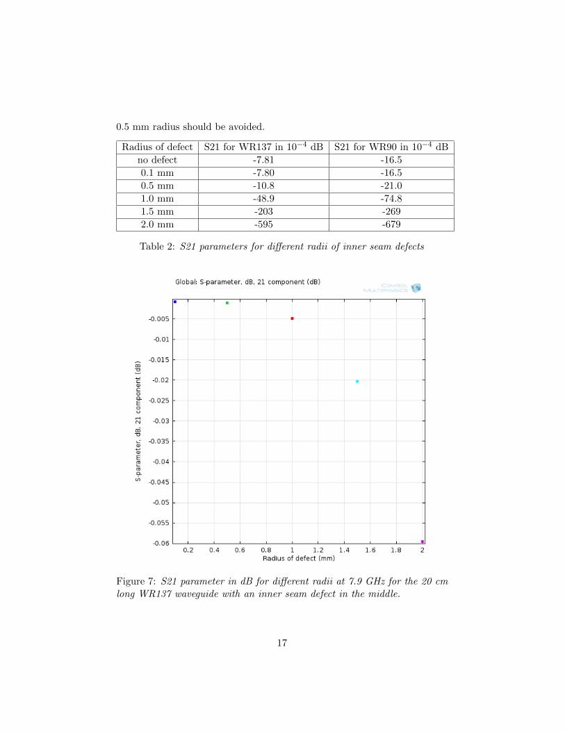
0.5 mm radius should be avoided.
Radius of defect S21 for WR137 in 10−4 dB S21 for WR90 in 10−4 dB
no defect -7.81 -16.5
0.1 mm -7.80 -16.5
0.5 mm -10.8 -21.0
1.0 mm -48.9 -74.8
1.5 mm -203 -269
2.0 mm -595 -679
Table 2: S21 parameters for different radii of inner seam defects
Figure 7: S21 parameter in dB for different radii at 7.9 GHz for the 20 cmlong WR137 waveguide with an inner seam defect in the middle.
17

3.2.2 Outer seam
The seam does not necessarily have to be bent inward but could also be bentoutward. For this model the same cylindrical approach is used. The sameeffects as in the inner seam model are found; reflections lead to a standingwave and the electric field is enhanced only at the edge (Figure 8). Insidethe half-cylindrical bent the electric field is zero even at the maximum of theelectric field of the TE10 mode. In this model the radius of the cylinders isalso varied and the simulation of the S21 parameters for different radii leadsto a qualitatively similar shape as for the inner seam. For comparison withthe inner seam, all values are summarized in Table 3. The outer seam reducesthe transmission less than the inner seam does, which can be explained bythe electric field not penetrating into the new cylindrical cavity.
(a) Standing wave between input portand defect.
(b) Norm of the electric field at the de-fect.
Figure 8: Norm of the electric field in the outer seam model.
S21 in 10−4 dBWR137 WR90
Radius of defect inner seam outer seam inner seam outer seam
no defect -7.81 -7.81 -16.5 -16.50.1 mm -7.80 -7.80 -16.5 -16.50.5 mm -10.8 -8.35 -21.0 -18.31.0 mm -48.9 -19.5 -74.8 -49.11.5 mm -203 -70.8 -269 -1872.0 mm -595 -211 -679 -561
Table 3: S21 parameters for different radii of seam defects.
18
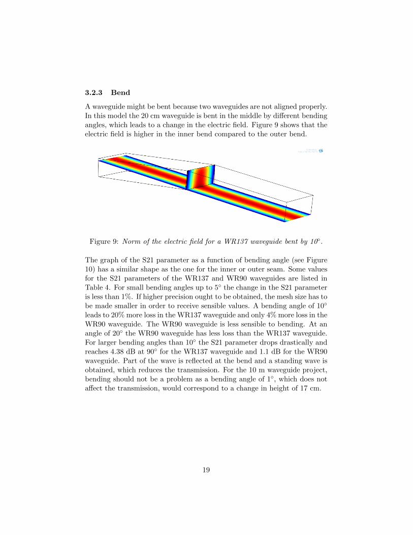
3.2.3 Bend
A waveguide might be bent because two waveguides are not aligned properly.In this model the 20 cm waveguide is bent in the middle by different bendingangles, which leads to a change in the electric field. Figure 9 shows that theelectric field is higher in the inner bend compared to the outer bend.
Figure 9: Norm of the electric field for a WR137 waveguide bent by 10◦.
The graph of the S21 parameter as a function of bending angle (see Figure10) has a similar shape as the one for the inner or outer seam. Some valuesfor the S21 parameters of the WR137 and WR90 waveguides are listed inTable 4. For small bending angles up to 5◦ the change in the S21 parameteris less than 1%. If higher precision ought to be obtained, the mesh size has tobe made smaller in order to receive sensible values. A bending angle of 10◦
leads to 20% more loss in the WR137 waveguide and only 4% more loss in theWR90 waveguide. The WR90 waveguide is less sensible to bending. At anangle of 20◦ the WR90 waveguide has less loss than the WR137 waveguide.For larger bending angles than 10◦ the S21 parameter drops drastically andreaches 4.38 dB at 90◦ for the WR137 waveguide and 1.1 dB for the WR90waveguide. Part of the wave is reflected at the bend and a standing wave isobtained, which reduces the transmission. For the 10 m waveguide project,bending should not be a problem as a bending angle of 1◦, which does notaffect the transmission, would correspond to a change in height of 17 cm.
19

Bending angle S21 for WR137 in 10−4 dB S21 for WR90 in 10−4 dB
no defect -7.81 -16.5
2◦ -7.82 -16.5
4◦ -7.86 -16.5
6◦ -8.00 -16.5
8◦ -8.34 -16.7
10◦ -9.34 -17.1
20◦ -35.4 -26.9
30◦ -159 -72.2
Table 4: S21 parameters for different bending angles for the 20 cm longWR137 and WR90 waveguide.
Figure 10: S21 parameters for different bending angles of the WR137 waveg-uide.
20

3.2.4 Rotation
At the intersection points, where two pieces of a waveguide are screwedtogether, a rotation can occur along the long axis. In this model flangeshave to be included to simulate the defects due to the rotation. At theintersection a sharp kink appears and the flange protrudes (see Figure 11).Due to the flanges the waveguide is only open for rotation angles of around10◦. In the simulations ’impedance boundary condition’ can not be assignedto the inside surfaces of the flanges because they have a metal bulk piecebehind them. So the option ’perfect electric conductor’ is chosen for thatpart. In a perfect electric conductor the electric field does not penetratethe surface while the option ’impedance boundary condition’ allows for anexponential decay of the electric field inside the material, which leads toloss. In this case the reference system corresponds to a rotation angle of 0◦
because it contains a loss-less perfect conductor surface in contrast to theother cases.
(a) 2 WR137 waveguides rotate by 2◦
with respect to each other.(b) Inside view: the white surface of theflange can be seen.
Figure 11: Rotated waveguide model.
The values for the S21 parameters in the rotation model are displayed inTable 5. The dependance of S21 on the rotation angle shows a similarcurve as for the bending angle. The dependance of the rotation angle ishowever stronger. Therefore the waveguides should be properly aligned inthis direction. Again the WR90 waveguide is more robust to rotation defects,but has a higher resistive loss without defects.
21

Rotation angle S21 for WR137 in 10−4 dB S21 for WR90 in 10−4 dB
0◦ -7.57 -16.0
1◦ -7.76 -16.1
2◦ -9.05 -16.5
3◦ -13.4 -17.9
4◦ -23.7 -21.2
5◦ -43.8 -27.6
6◦ -78.6 -38.1
7◦ -134 -54.8
8◦ -217 -79.4
9◦ -336 -113
10◦ -500 -160
Table 5: S21 parameters for different rotation angles for the 20 cm longWR137 and WR90 waveguide.
3.2.5 Pyramid defect
In order to simulate a point defect inside the waveguide, an object with theshape of a pyramid as shown in Figure 12(a) was chosen. Such defects canfor example arise from production errors and dirt deposition. The shape ofthe defect should not be symmetric in order to avoid special behavior likestanding waves due to the symmetry of the system. Therefore, a pyramidseems to be an appropriate choice which COMSOL offers. The pyramidconcentrates the electric field at its peak (compare Figure 12(b)).
(a) The pyramid used in the pyra-mid models.
(b) The modified electric field around thepyramid defect.
Figure 12: The pyramid model.
In this simulation the height of the pyramid is varied and the S21 parameteris investigated. The result is displayed in Figure 13 for the WR137 waveg-
22

uide. The curve shows a similar shape for both waveguides. For heights upto 0.8 mm no significant effect can be observed in Table 6.
Figure 13: One pyramid: S21 parameter in 10−4 dB for different heights ofthe pyramid defect at 7.9 GHz for the 20 cm long WR137 waveguide.
3.2.6 Many pyramid defects
In the real waveguide the whole surface is rough. This is simulated byusing a large amount of pyramid defects. Due to limited computationalresources, the amount of pyramids is limited to 45. Using the ’copy’ optionin COMSOL, the pyramid is duplicated and displaced, which leads to a gridof pyramids as it is shown in Figure 14. The dimensions of the pyramids canbe varied up to 1 mm because the pyramids intersect. For larger dimensionsthis leads to boundaries with wrongly defined boundary conditions. Table6 indicates that the difference between one or 45 pyramid defects is below7% for the WR137 waveguide and below 20% for the WR90 waveguide forthe simulated dimensions. The focus should therefore lay on minimizing theheight of the defects instead of the number of point defects.
23

Figure 14: The surface with 45 pyramid defects.
S21 in 10−4 dBWR137 WR90
Height of pyramid 1 pyramid 45 pyramids 1 pyramid 45 pyramids
no defect -7.81 -7.81 -16.5 -16.50.1 mm -7.81 -7.81 -16.5 -16.50.2 mm -7.81 -7.81 -16.5 -16.50.4 mm -7.82 -7.83 -16.5 -16.60.6 mm -7.82 -7.91 -16.6 -16.90.8 mm -7.89 -8.18 -16.9 -18.31.0 mm -7.97 -8.56 -17.4 -20.9
Table 6: S21 parameters for different heights of pyramid defects.
3.2.7 Conclusion
The S21 parameter shows the same dependance on the size of the imperfec-tion for all the different kind of defects. The main difference is the magni-tude of the effect. It is obvious that defects should be as small as reasonablyachievable. The simulation results can be used to decide if a certain typeof imperfection should be made smaller. The results also give suggestionson how the waveguides can be constructed. Some defects can be minimizedor avoided easier than others. Therefore one should focus on those thatcan be minimized easily or lead to a relatively large improvement in thetransmission.
24
3.3 Coupling into the cavity
In this section the coupling between a coaxial cable and a 3D cavity isinvestigated. For the coaxial cable the parameters of the UT-085C-Al-TP-LL cable is used. This cable has a outer conductor with radius R = 1.09855mm made out of aluminum and an inner conductor with radius r = 0.287mm made out of silver plated copper [6]. Between the two conductors PTFEis used as a dielectric filling. Inside the cavity vacuum is assumed. Theelectrical conductivities and the relative permittivity for the materials arestated in section 3.1.2. For the cavity the dimensions a and b of the WR137waveguide are used. The eigenfrequency of the cavity is chosen to be 7.9GHz by adapting the length d. In the model two coaxial cables are attachedto the top of the waveguide. One will act as the input port and the otheras the output port. Figure 15a gives an overview of the model. In thesimulations two main questions are examined:
• How does the position of the coaxial cable on the surface of the cavityinfluence the loaded, the internal and the external quality factor of thesystem? How is the coupling affected?
• How does the length of the inner conductor and dielectric extendinginto the cavity influence the coupling?
(a) The model - an overview. (b) The coaxial cable with the dielectricin blue 3 mm above the surface of thecavity. The cylinder with the small ra-dius is the inner conductor, the other theouter conductor.
Figure 15: Model of the two coaxial cables coupled to the cavity.
25

3.3.1 Influence of the position of the coaxial cable
The question concerning the influence of the position of the coaxial cablewill be answered first. Using the model described above, three values willbe varied:
• The position in x-direction: coaxX
• The position in z-direction: coaxZ
• The length of the inner conductor protruding from the dielectric:coaxin
The coordinates are chosen such that the cavity has width a in x-direction,height b in y-direction and length d in z-direction. Since the cavity surfaceis point symmetric to the center, the positions of the input coaxial cablesare only varied in one forth of the surface as it is depicted in the schematicof Figure 16. The cables are placed periodically with a distance of 4 mm inx-direction and 3 mm in y-direction. The starting position is chosen so thatthe last cable in each row or column is positioned in the middle. In eachsimulation one cable is used as the input and the other as the output cable.The two cables are placed point symmetrically with respect to the center ofthe surface. Therefore the middle coaxial cable is left away.
34.849 mm17.4245 mm
22.621 mm
11.3105 mm
coaxX �
coaxZ
¯
Figure 16: The big rectangle represents the top surface of the cavity. Theblack circles are the positions of the input coaxial cable, the dashed circlesbelong to the output cables placed symmetrically to the center. The positionof the input cables is labeled with coaxX along the horizontal axis and withcoaxZ along the vertical axis.
26

For each of the 19 positions the length of the inner conductor sticking out ofthe dielectric is varied from 1 mm to 4 mm. The outer conductor is attachedto the cavity and the dielectric is cut off 3 mm above the cavity (comparewith Figure 15b). This means that for coaxin = 3 mm the inner conductor isat the same height as the surface of the cavity, for coaxin = 4 mm it emerges1 mm into the cavity. In a first set of simulations the resonant frequency f0and the loaded quality factor QL of the system is computed. This data isthen used to calculate the appropriate frequency spectrum over which theS21 parameter should be computed. The bandwidth δf of the Lorentzianfunction can be assessed using equation (18). The calculated bandwidth isdoubled in order to cover a nice range of the Lorentzian function and thendivided into 20 equally spaced frequency points at each side of the resonantfrequency. The simulation is run to calculate the S21 parameter for eachof the 41 frequencies at each position of the coaxial cable. The data setsare exported and analysed with Mathematica, where the fitting routine forthe Lorentzian function is done. An characteristic example can be seen inFigure 17.
coaxX = 5.4245 mm
coaxZ = 11.3105 mm
coaxin = 2 mm
7.89965 7.89970 7.89975 7.89980 7.89985 7.89990f @GHzD
0.00002
0.00004
0.00006
0.00008
S_21
Figure 17: A Lorentzian fit for the S21 parameter as a function of frequency.The input coaxial cable is positioned at the place indicated on the figure.
The loaded quality factor extracted from the Lorentzian fit is in agreementwith the one which COMSOL computed. Using equation (22) and (23), theexternal and internal quality factor is calculated. The internal quality factoris between 112’000 and 130’000 for all configurations. The external qualityfactor is highly dependent on the length the coaxial cable protruding from
27

the dielectric. For 1 and 2 mm the external quality factor is above 108 forcoaxin = 1 mm and above 106 for coaxin = 2 mm. This means that theloaded quality factor is about as high as the internal quality factor. For alength of 3 or 4 mm, when the inner conductor of the coaxial cable reachesthe surface of the cavity (coaxin = 3 mm) or extends into the cavity (coaxin= 4 mm), the coupling is strongly increased. The loaded quality factor QLdepends also on the position of the coaxial cable on the surface of the cavity.This can be seen in Figure 18. Positions which are closer to the center lead tostronger coupling into the TE101 mode of the cavity. This can be explainedby the mode structure.
0.004 0.006 0.008 0.010
0.005
0.010
0.015
coaxZ @mD
coaxX
@mD
Q_L
40 000
60 000
80 000
100 000
120 000
-6-4-20246
Figure 18: The loaded quality factor for different positions of the coaxialcable in x-direction (coaxX) and in z-direction (coaxZ) with coaxin = 3 mm.
Focusing on one fixed position in z-direction, the dependence of the qualityfactors on the x-position coaxX can be investigated in more detail. This isdone in Figure 19. For x-positions of the coaxial cable on the side of the cav-ity, the external quality factor is larger than Qint. Moving the cable towardsthe center leads to a decrease in the external quality factor (see Figure 20a)because the coupling into the TE101 mode of the cavity is stronger in thecenter.
28
Q_L Q_int Q_ext
0.000 0.005 0.010 0.015
2 ´ 104
5 ´ 104
1 ´ 105
2 ´ 105
5 ´ 105
1 ´ 106
coaxX @mD
Q
(a) The z-direction was fixed at coaxZ = 2.3105 mm.
Q_L Q_int Q_ext
0.000 0.002 0.004 0.006 0.008 0.010 0.012
5000
1 ´ 104
2 ´ 104
5 ´ 104
1 ´ 105
coaxX @mD
Q
(b) The z-direction was fixed at coaxZ = 11.3105 mm.
Figure 19: The loaded quality factor (blue), the internal quality factor (pur-ple) and the external quality factor (green) for different positions of thecoaxial cable in x-direction. The length of the inner conductor sticking outof the dielectric was 4 mm.
29

0.004 0.006 0.008 0.010
0.005
0.010
0.015
coaxZ @mD
coaxX
@mD
LogHQ_extL for coaxin = 4 mm
3.5
4.0
4.5
5.0
5.5
6.0
-6-4-20246
(a) The logarithm of the external quality factor.
0.004 0.006 0.008 0.010
0.005
0.010
0.015
coaxZ @mD
coaxX
@mD
Coupling Κ_ext�2Π = f0�Q_ext in MHz
0.5
1.0
1.5
2.0
2.5
3.0
-6-4-20246
(b) The external coupling κext/2π in MHz
Figure 20: The logarithm of the external quality factor and the external cou-pling coefficient in MHz for different positions (coaxX, coaxZ) of the coaxialcable and with coaxin = 4 mm.
30

For positions closer to the center Qext reaches the internal quality factorQint, where critical coupling is achieved, and continues to decrease. Here theloaded quality factor is dominated by the external one and is at a minimumclose to the center of the cavity surface. The coupling between the coaxialcables and the cavity can be characterized by the external coupling coefficentκext/2π given by equation (24) and plotted in Figure 20b.
3.3.2 Influence of the conductors and the dielectric
In the previous section we have seen that the external quality factor dependson the position of the coaxial cable and the length of the inner conductor.In order to investigate the effect of the length of the inner conductor andthe position of the dielectric above the cavity, the position of the cable isfixed to one specific position (coaxX = 6.4245 mm, coaxZ = 6.13105 mm).In the first layout, the length of the inner conductor sticking out of thedielectric is varied from coaxin = 0 mm (cut off at the same place as thedielectric) to coaxin = 5 mm (extending 2 mm into the cavity). In thesecond layout, coaxin is fixed to 2 mm while the whole dielectric and innerconductor combination is varied from 3 mm above the cavity down to thesurface of the cavity. Figure 21 illustrates the different layouts. A thirdlayout where the inner conductor is cut off right at the dielectric (coaxin =0 mm) is also calculated and the same characteristics can be seen.
(a) Layout 1 and 2. Withcoaxin = 2 mm and thedielectric 3 mm above thecavity.
(b) Layout 1. With coaxin= 4 mm and the dielectric3 mm above the cavity.
(c) Layout 2. With coaxin= 2 mm and the dielectric1 mm above the cavity.
Figure 21: The different layouts to analyse the influence of the conductorsand the dielectric.
31

Impact of the length of the inner conductor (Layout 1)As in the previous simulation, the loaded quality factor and the resonantfrequency are computed for different lengths of the inner conductor. Thesetwo values are then used to choose an appropriate frequency range for thefrequency sweep. The different Lorentzian functions can be seen in Figure22. The resonant frequency does not strongly depend on the inner conductorlengths between coaxin = 0 mm to coaxin = 3 mm and is 7.8997 GHz. If theinner conductor extends into the cavity, the resonant frequency is lowered -for example by 7.2 MHz for coaxin = 5 mm.
Figure 22: The S21 parameter as a function of frequency around the res-onance frequency for different length of the inner conductor sticking out ofthe dielectric (coaxin).
From the Lorentzian fit, the internal and the external quality factors areobtained and displayed logarithmically in Figure 23. The internal qualityfactor varies from 109’000 to 125’000 as can be seen in Table 7. The externalquality factor decreases exponentially with the length of the inner conductorprotruding from the dielectric. At the chosen position of the coaxial cableon top of the cavity, the resonator is under-coupled if the inner conductordoes not extend into the cavity.
32

Q_L Q_int Q_ext
1 2 3 4 5
coaxin @mmD
105
107
109
1011
Q
Figure 23: The internal, external and loaded quality factors for differentlengths of the inner conductor sticking out of the dielectric.
1 2 3 4 5coaxin @mmD
0.5
1.0
1.5
2.0
2.5
3.0
3.5
Coupling Κ_ext�2Π in MHz
Figure 24: The external coupling coefficient in MHz for different lengths ofthe inner conductor sticking out of the dielectric.
33

The coupling between the coaxial cables and the cavity is described by theexternal coupling coefficent κext/2π, which is plotted in Figure 24. Theexternal coupling coefficient varies over 8 orders of magnitude from 0.07 Hz(coaxin = 0 mm) to 3.40 MHz (coaxin = 5 mm) as summarized in Table7. If the inner conductor extends into the cavity, couplings in the MHzregime can be obtained. In conclusion, the external coupling can be chosenby varying the length of the inner conductor.
coaxin κext/2π Qint0 mm 0.07 Hz 125’000
1 mm 5.53 Hz 123’000
2 mm 465 Hz 124’000
3 mm 31.8 kHz 123’000
4 mm 582 kHz 120’000
5 mm 3.40 MHz 109’000
Table 7: The external coupling coefficient and the internal quality factor fordifferent lengths of the inner conductor sticking out of the dielectric.
Impact of the position of the dielectric (Layout 2)The same analysis is done for layout 2, where the height of the dielectricabove the cavity is changed. The length of the inner conductor protrudingfrom the dielectric is fixed to 2 mm. Figure 25 shows that the coupling islarger for dielectric and inner conductor compositions that are close to thesurface of the cavity. The values for the external coupling coefficient aredisplayed in Table 8 along with the internal quality factors. The internalquality factor is also influenced by the position of the dielectric, which isplotted in Figure 26. If the inner conductor does not extend into the cavity,Qint has a constant value of 124’000. The internal quality factors are thesame for both layout 1 and 2 for corresponding inner conductor end posi-tions. This can be seen in the example of the inner conductor emerging 1mm into the cavity: in layout 1 this corresponds to coaxin = 4 mm andin layout 2 to a dielectric of 1 mm height above the cavity. Both have aninternal quality factor of 120’000. The external coupling is of the same orderof magnitude for corresponding inner conductor end positions, but it is notthe same for the two layouts if the inner conductor emerges into the cavity.In the example where the inner conductor emerges 1 mm into the cavity,the coupling is reduced in layout 2 with 490 kHz compared to layout 1 with582 kHz. In layout 2 the dielectric covers more of the inner conductor andaffects the coupling. In conclusion, the height of the dielectric above the cav-
34

ity does not influence the internal quality factor, but can have a screeningeffect reducing the coupling.
Height above cavity 0.2 mm 1 mm 2 mm 3 mm
κext/2π 1.98 MHz 490 kHz 29.4 kHz 462 Hz
Qint 113’000 120’000 123’000 124’000
Table 8: The external coupling coefficient and the internal quality factor fordifferent heights of the dielectric and inner conductor composition above thecavity.
0.5 1.0 1.5 2.0 2.5 3.0empty space @mmD
0.5
1.0
1.5
2.0
Coupling Κ_ext�2Π in MHz
Figure 25: The external coupling coefficient in MHz for different heights ofthe dielectric above the cavity.
0.5 1.0 1.5 2.0 2.5 3.0empty space @mmD
114 000
116 000
118 000
120 000
122 000
124 000
Q_int
Figure 26: The internal quality factor for different heights of the dielectricabove the cavity.
35

3.4 Coupling cavity and waveguide
The model of the cavity with the two coaxial cables is now extended byadding the waveguide. The coupling from the cavity to the waveguide canbe conducted by a aperture in the cavity and the waveguide. This aperaturemay be circular or rectangular and can be positioned at various differentplaces. An antenna can also be inserted. The size, shape and position of theaperture influences the internal quality factor of the cavity and the couplingto the waveguide. An analysis of the different options is therefore necessary.The cavity and the waveguide are separated by a wall which has a certainthickness in experiments and is not infinitesimally small as in literature [8].In this project a circular aperture with radius 4 mm is chosen. In the modeldescribed below, the waveguide is coupled to the side of the cavity (seeFigure 27) where the dimensions a and b of the cavity and the waveguidematch. The coaxial cables are placed at the same positions as described insection 3.3.2. The dielectric ends 2 mm above the cavity surface and theinner conductor sticks 3 mm out of the dielectric.
Figure 27: The model of the cavity coupled to the waveguide.
To investigate the coupling, three ports are defined:
• Input port 1 is the left coaxial cable.
• Output port 2 is the right coaxial cable.
• Output port 3 is at the end of the waveguide.
36

Same as in the other simulations, the resonant frequency and the loadedquality factor are obtained first and used to calculate the frequency rangefor the frequency sweep. Two different S-parameters are computed: the S21parameter characterizing the transmission from one coaxial cable throughthe cavity to the other and the S31 parameter characterizing the transmis-sion from the input coaxial cable into the cavity and through the waveguide.From the S21 and the S31 parameters two different sets of external qualityfactors are obtained (see Figure 28). The loaded quality factor is the same.
Qextcoax
Qextwaveguide
1 2 3 4 5 6 7
10 000
50 000
20 000
30 000
15 000
70 000
thickness @mmD
Q
Figure 28: The external quality factors for different wall thicknesses. Qcoaxext
is obtained from the S21 parameter and Qwaveguideext from the S31 parameter.The radius of the hole is fixed to 4 mm.
From the two external quality factors, the coupling between the coaxialcables and the coupling between the coaxial cable and the waveguide can becomputed (see Figure 29). The coupling between the coaxial cables obtainedfrom S21 does not depend on the thickness of the wall. For thicker wallsthe coupling from the coaxial cable into the waveguide is reduced. In thisexample the coupling into the waveguide is larger than the coupling into thecoaxial cable for wall thicknesses below 3.5 mm. A thinner wall leads to a
37

larger coupling to the waveguide.
Κcoax�2Π Κ
waveguide�2Π
1 2 3 4 5 6 7
200
400
600
800
1000
1200
1400
1600
thickness @mmD
Coupling
inkH
z
Figure 29: The external coupling coefficients for different wall thicknesses.κcoax/2π describes the coupling between the coaxial cables in presence of acavity and a waveguide (from S21). κwaveguide/2π describes the coupling intothe cavity and through the waveguide (from S31).
38

4 Conclusion
Rectangular waveguides show low transmission loss over long distances. Oursimulations of different defects have shown that the transmission is not sig-nificantly affected by small defects. The obtained transmission tables forthe different defects can be used to decide if the present defects should beminimized in experiments. They also give hints on how to construct a longwaveguide.In the second set of simulations, the coupling to the cavity through coaxialcables is understood. By varying the position of the coaxial cables on thesurface of the cavity, the length of the inner conductor sticking out of thedielectric and the end position of the dielectric, the desired coupling can beengineered.By adding the waveguide to the model of the cavity, the coupling to thewaveguide can be simulated. One version of many was analysed in moredetail. By choosing the thickness of the wall between the cavity and thewaveguide as well as the radius of the hole, the coupling to the waveguidecan be adjusted.
5 Outlook and Acknowledgements
The ”SuperQuNet” project is still at the beginning and a lot of work hasto be done until the loop-hole free Bell-Tests can be realized. Regardingthe waveguide, the coupling from the cavity into the waveguide has to beinvestigated further. Many options are possible and only one is analyzed inthis thesis. In order to optimized the system layout, the required couplingshould be identified. At the moment parameters are varied to examine theirgeneral influence on the coupling strength without knowing which values toaim at. Also the whole system has not been simulated yet. Adding thesecond cavity and its two coaxial cables may lead to further changes in thetransmission properties. Measurements of the attenuation of coaxial cablesand waveguides are made at room and liquid helium temperature. Furthermeasurements can be done concerning the coupling.
I would like to take this opportunity to thank Philipp Kurpiers for his guid-ance and assistance on the project. Many models and analysis were devel-opped together. The discussions were fruitful and led to new insights. Healso showed me how to measure S-parameters for coaxial cables and waveg-uides at room and liquid helium temperature. I have learned a lot and it
39

was a pleasure to work with Philipp Kurpier.I would also like to thank Prof. Andreas Wallraff for giving me the optionto work on this project. I enjoyed the nice atmosphere in the group.
References
[1] A. Aspect, et al., Experimental Test of Bell’s Inequalities Using Time-Varying Analyzers, Phys. Rev. Lett. 49, 25, 1804 (1982).
[2] M. Ansmann, et al., Violation of Bell’s inequality in Josephson phasequbits, Nature 461, 7263, 504 (2009).
[3] C. A. Balanis, Circular Waveguides, John Wiley & Sons, Inc. (2005).
[4] COMSOL, RF Module, http://www.comsol.com/rf-module (23.9.2013).
[5] M. Goppl, A. Fragner, M. Baur, R. Bianchetti, S. Filipp, J. M. Fink,P. J. Leek, G. Puebla, L. Steffen, and A. Wallraff, Coplanar waveg-uide resonators for circuit quantum electrodynamics, Journal of AppliedPhysics, 104:113904 (2008).
[6] Micro-Coax, UT-085C-AL-TP-LL,http://www.micro-coax.com/products/product-details/?type=alumiline&part id=75 (25.2.2014).
[7] Penn Engineering, Waveguide Sizes and Data,http://www.pennengineering.com/waveguide.php (30.9.2013).
[8] David M. Pozar, Microwave Engineering, Fourth Edition, John Wiley& Sons, Inc. (2012).
[9] P-N Designs, Waveguide Primer,http://www.microwaves101.com/encyclopedia/waveguide.cfm(19.2.2014).
[10] G. Weihs, et al., Violation of Bell’s Inequality under Strict EinsteinLocality Conditions, Phys. Rev. Lett. 81, 23, 5039 (1998).
40

Copyright © 2022 FDOKUMEN