Photonics Devices Based on Hybrid Approach Combining Liquid Crystals and Sol-Gel Waveguides
21
This article was downloaded by: [Consiglio Nazionale delle Ricerche] On: 19 February 2014, At: 09:38 Publisher: Taylor & Francis Informa Ltd Registered in England and Wales Registered Number: 1072954 Registered office: Mortimer House, 37-41 Mortimer Street, London W1T 3JH, UK Fiber and Integrated Optics Publication details, including instructions for authors and subscription information: http://www.tandfonline.com/loi/ufio20 Photonics Devices Based on Hybrid Approach Combining Liquid Crystals and Sol-Gel Waveguides L. Sirleto a , G. Coppola a , G. C. Righini b & G. Abbate c a Institute for Microelectronics and Microsystems (IMM) Italian National Research Council , Napoli, Italy b Istituto di Fisica Applicata “Nello Carrara” Italian National Research Council , Firenze, Italy c INFM and Physics Department , University of Naples “Federico II” , Napoli, Italy Published online: 15 Aug 2006. To cite this article: L. Sirleto , G. Coppola , G. C. Righini & G. Abbate (2006) Photonics Devices Based on Hybrid Approach Combining Liquid Crystals and Sol-Gel Waveguides, Fiber and Integrated Optics, 25:3, 175-194, DOI: 10.1080/01468030600569800 To link to this article: http://dx.doi.org/10.1080/01468030600569800 PLEASE SCROLL DOWN FOR ARTICLE Taylor & Francis makes every effort to ensure the accuracy of all the information (the “Content”) contained in the publications on our platform. However, Taylor & Francis, our agents, and our licensors make no representations or warranties whatsoever as to the accuracy, completeness, or suitability for any purpose of the Content. Any opinions and views expressed in this publication are the opinions and views of the authors, and are not the views of or endorsed by Taylor & Francis. The accuracy of the Content should not be relied upon and should be independently verified with primary sources of information. Taylor and Francis shall not be liable for any losses, actions, claims, proceedings, demands, costs, expenses, damages, and other liabilities whatsoever or howsoever caused arising directly or indirectly in connection with, in relation to or arising out of the use of the Content. This article may be used for research, teaching, and private study purposes. Any substantial or systematic reproduction, redistribution, reselling, loan, sub-licensing, systematic supply, or distribution in any form to anyone is expressly forbidden. Terms & Conditions of access and use can be found at http:// www.tandfonline.com/page/terms-and-conditions
-
Upload
independent -
Category
Documents
-
view
1 -
download
0
Transcript of Photonics Devices Based on Hybrid Approach Combining Liquid Crystals and Sol-Gel Waveguides
This article was downloaded by: [Consiglio Nazionale delle Ricerche]On: 19 February 2014, At: 09:38Publisher: Taylor & FrancisInforma Ltd Registered in England and Wales Registered Number: 1072954 Registered office: Mortimer House,37-41 Mortimer Street, London W1T 3JH, UK
Fiber and Integrated OpticsPublication details, including instructions for authors and subscription information:http://www.tandfonline.com/loi/ufio20
Photonics Devices Based on Hybrid ApproachCombining Liquid Crystals and Sol-Gel WaveguidesL. Sirleto a , G. Coppola a , G. C. Righini b & G. Abbate ca Institute for Microelectronics and Microsystems (IMM) Italian National Research Council ,Napoli, Italyb Istituto di Fisica Applicata “Nello Carrara” Italian National Research Council , Firenze, Italyc INFM and Physics Department , University of Naples “Federico II” , Napoli, ItalyPublished online: 15 Aug 2006.
To cite this article: L. Sirleto , G. Coppola , G. C. Righini & G. Abbate (2006) Photonics Devices Based on HybridApproach Combining Liquid Crystals and Sol-Gel Waveguides, Fiber and Integrated Optics, 25:3, 175-194, DOI:10.1080/01468030600569800
To link to this article: http://dx.doi.org/10.1080/01468030600569800
PLEASE SCROLL DOWN FOR ARTICLE
Taylor & Francis makes every effort to ensure the accuracy of all the information (the “Content”) containedin the publications on our platform. However, Taylor & Francis, our agents, and our licensors make norepresentations or warranties whatsoever as to the accuracy, completeness, or suitability for any purpose of theContent. Any opinions and views expressed in this publication are the opinions and views of the authors, andare not the views of or endorsed by Taylor & Francis. The accuracy of the Content should not be relied upon andshould be independently verified with primary sources of information. Taylor and Francis shall not be liable forany losses, actions, claims, proceedings, demands, costs, expenses, damages, and other liabilities whatsoeveror howsoever caused arising directly or indirectly in connection with, in relation to or arising out of the use ofthe Content.
This article may be used for research, teaching, and private study purposes. Any substantial or systematicreproduction, redistribution, reselling, loan, sub-licensing, systematic supply, or distribution in anyform to anyone is expressly forbidden. Terms & Conditions of access and use can be found at http://www.tandfonline.com/page/terms-and-conditions
Fiber and Integrated Optics, 25:175–194, 2006Copyright © Taylor & Francis Group, LLCISSN: 0146-8030 print/1096-4681 onlineDOI: 10.1080/01468030600569800
Photonics Devices Based on Hybrid ApproachCombining Liquid Crystals and Sol-Gel
Waveguides
L. SIRLETOG. COPPOLA
Institute for Microelectronics and Microsystems (IMM)Italian National Research CouncilNapoli, Italy
G. C. RIGHINI
Istituto di Fisica Applicata “Nello Carrara”Italian National Research CouncilFirenze, Italy
G. ABBATE
INFM and Physics DepartmentUniversity of Naples “Federico II”Napoli, Italy
In this article, the analysis of both an integrated electro-optic switch and a contin-uously tunable filter based on a Bragg grating in planar waveguide with a liquidcrystal overlayer is reported. The fast and bistable switching of smectic C∗ in thesurface-stabilized liquid crystal structure has been utilized in order to investigate thepossibility of realizing an integrated electro-optical switch, whereas the soft-mode ofsmectic A∗ liquid crystals, allowing a continuous modulation of extraordinary refrac-tive index, have been utilized in order to design an integrated wavelength filter in thewavelength range of interest for optical communication. Moreover, the performanceof an electro-optical router, working at the wavelength of 1.55 µm and based onthe multimode interference effects together with the electro-optic effect of smectic A∗liquid crystal, is theoretically and numerically discussed.
Keywords integrated optics, electro-optic devices, liquid crystal devices, Bragggrating, multi-mode interference effect, optical switch, optical tunable filter, routingdevices
Received 18 May 2005; accepted 21 December 2005.Address correspondence to L. Sirleto, Institute for Microelectronics and Microsystems (IMM),
Italian National Research Council, Via P. Castellino 111, I-80131, Napoli, Italy. E-mail: [email protected]
175
Dow
nloa
ded
by [
Con
sigl
io N
azio
nale
del
le R
icer
che]
at 0
9:38
19
Febr
uary
201
4
176 L. Sirleto et al.
Introduction
The research on materials for integrated optics is continuously in progress to achieveever better performance. In this context, glass-integrated optics has attracted a greatinterest due to its advantages: robustness, appealing optical properties, and compatibilitywith established silicon manufacturing protocols. Among techniques for fabricating glass-integrated optics structures, sol-gel processing has gained considerable attention in recentyears; it is justified by the versatility of process, which allows the production of glasseswith largely different physical-chemical properties just by changing the starting solutioncomposition. So, it is possible to tune up the refractive index of the produced film overa very large interval; e.g., using silica-titania binary glasses, the refractive index maybe varied approximately from 1.5 up to 2.3. This characteristic allows matching thedesign of the guiding structure to the specific needs of the devices. Other fundamentaladvantages of the sol-gel process are the relatively low processing temperature, the lowcost of production, and low-loss connection to single-mode optical fibers [1, 2]. Theonly major disadvantage is the current lack of an operating mechanism for switching andwavelength tuning filtering.
To make compact devices it is desirable to have active control of light over shortdistances in integrated optical circuits. Liquid crystals have effective electro-optic co-efficients orders of magnitude larger than their solid-state counterparts [3] due to theiranisotropy and large electric field–induced molecular reorientation. These properties,combined with low-cost process technology, make liquid crystals interesting as electro-optically active waveguide materials for organic integrated optics whenever compactness,complexity, and low cost are more important requirements than switching speed. There-fore, in recent years, several authors suggested and demonstrated the possibility of usingliquid crystals (LCs) materials to control the light propagation in optical guiding devices,as planar waveguides or cylindrical fibers [4–12].
In order to overcome the lack of mechanism for switching and filtering regardingsol-gel waveguides, we propose to combine them with liquid crystals. The electro-opticeffect of ferroelectric liquid crystals can be used in order to figure out active functions,whereas good quality waveguide could be realized by the sol-gel method.
Based on this line of argument, in this article, a number of integrated optic de-vices based on hybrid technology combining liquid crystals and sol-gel waveguide areinvestigated. First, we briefly explain the electro-optic effects of chiral smectic LCs.Then, design and analysis of electro-optical devices based on a Bragg grating integratedon a glass waveguide employing liquid crystal as cover are presented. In this structureit is possible to vary the Bragg mirror trasmittivity by means of the electro-optic ef-fect in smectic liquid crystals. Two different configurations can be obtained dependingon the particular liquid crystal employed as cover of the grating. The first is an in-tegrated fast electro-optic switch: combining a smectic C∗ liquid crystal [13–15] andthe selective properties of the Bragg grating, a variation of the device transmittivitycan be achieved. In this kind of device, the switching of the light intensity is obtainedby a shift of the Bragg grating spectral response. The device works as a switchablenotch filter in the optical domain. This feature allows overcoming the typical problemsof intensity-dependent devices. In the second configuration, the possibility of realizinga novel continuously tunable integrated filter in the range of optical communicationswavelengths has been explored. In this case, the cover of the Bragg grating is a smec-tic A∗ [16–18] LC, which allows continuous modulation of the extraordinary refractiveindex of the liquid crystal itself and consequently a continuous variation of the selective
Dow
nloa
ded
by [
Con
sigl
io N
azio
nale
del
le R
icer
che]
at 0
9:38
19
Febr
uary
201
4
Liquid Crystals and Sol-Gel Waveguides in Photonics Devices 177
properties of the device. This device, therefore, behaves as a tunable notch filter in theoptical domain.
Routing devices do not require very high switching time performances but have toguarantee low optical insertion loss and quite good performances in term of crosstalk[19–22]. A novel configuration for an integrated router, based on the mode-mixingprinciple together with the electro-optic effect of a smectic A∗ liquid crystal [16–18],working at the wavelength of 1.55 micron is theoretically discussed and numericallyanalyzed.
Electro-Optical Effects of Smectic Liquid Crystals
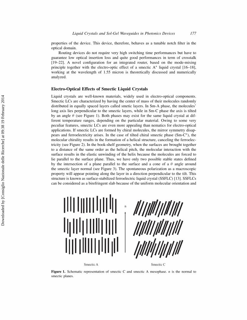
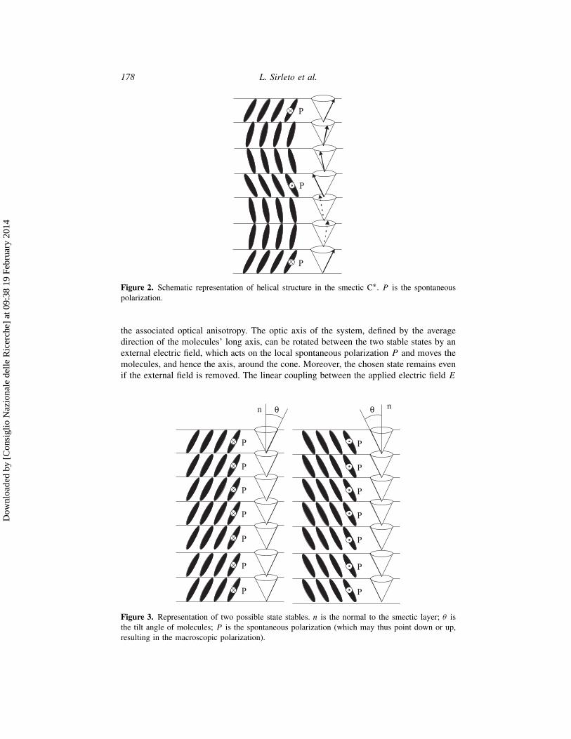
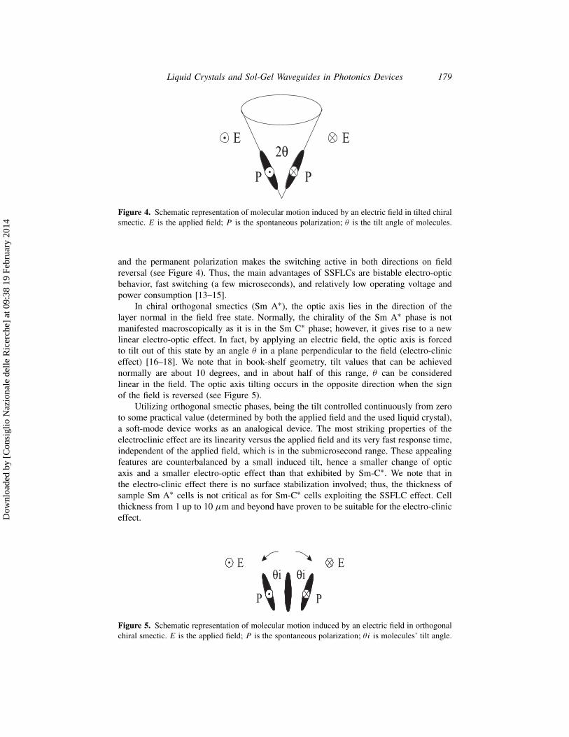
Liquid crystals are well-known materials, widely used in electro-optical components.Smectic LCs are characterized by having the center of mass of their molecules randomlydistributed in equally spaced layers called smetic layers. In Sm-A phase, the molecules’long axis lies perpendicular to the smectic layers, while in Sm-C phase the axis is tiltedby an angle θ (see Figure 1). Both phases may exist for the same liquid crystal at dif-ferent temperature ranges, depending on the particular material. Owing to some verypeculiar features, smectic LCs are even more appealing than nematics for electro-opticalapplications. If smectic LCs are formed by chiral molecules, the mirror symmetry disap-pears and ferroelectricity arises. In the case of tilted chiral smectic phase (Sm-C∗), themolecular chirality results in the formation of a helical structure, canceling the ferroelec-tricity (see Figure 2). In the book-shelf geometry, when the surfaces are brought togetherto a distance of the same order as the helical pitch, the molecular interaction with thesurface results in the elastic unwinding of the helix because the molecules are forced tolie parallel to the surface plane. Thus, we have only two possible stable states definedby the intersection of a plane parallel to the surface and a cone of a θ angle aroundthe smectic layer normal (see Figure 3). The spontaneous polarization as a macroscopicproperty will appear pointing along the layer in a direction perpendicular to the tilt. Thisstructure is known as surface-stabilized ferroelectric liquid crystal (SSFLC) [13]. SSFLCscan be considered as a birefringent slab because of the uniform molecular orientation and
Figure 1. Schematic representation of smectic C and smectic A mesophase. n is the normal tosmectic planes.
Dow
nloa
ded
by [
Con
sigl
io N
azio
nale
del
le R
icer
che]
at 0
9:38
19
Febr
uary
201
4
178 L. Sirleto et al.
Figure 2. Schematic representation of helical structure in the smectic C∗. P is the spontaneouspolarization.
the associated optical anisotropy. The optic axis of the system, defined by the averagedirection of the molecules’ long axis, can be rotated between the two stable states by anexternal electric field, which acts on the local spontaneous polarization P and moves themolecules, and hence the axis, around the cone. Moreover, the chosen state remains evenif the external field is removed. The linear coupling between the applied electric field E
Figure 3. Representation of two possible state stables. n is the normal to the smectic layer; θ isthe tilt angle of molecules; P is the spontaneous polarization (which may thus point down or up,resulting in the macroscopic polarization).
Dow
nloa
ded
by [
Con
sigl
io N
azio
nale
del
le R
icer
che]
at 0
9:38
19
Febr
uary
201
4
Liquid Crystals and Sol-Gel Waveguides in Photonics Devices 179
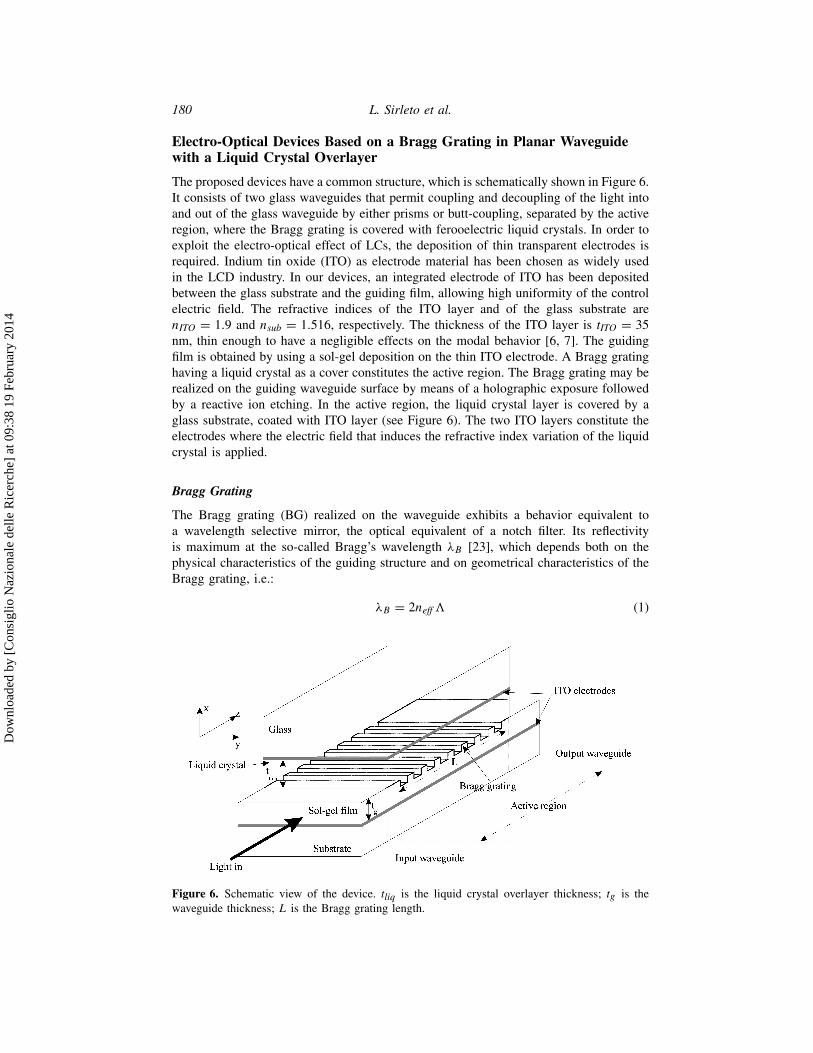
Figure 4. Schematic representation of molecular motion induced by an electric field in tilted chiralsmectic. E is the applied field; P is the spontaneous polarization; θ is the tilt angle of molecules.
and the permanent polarization makes the switching active in both directions on fieldreversal (see Figure 4). Thus, the main advantages of SSFLCs are bistable electro-opticbehavior, fast switching (a few microseconds), and relatively low operating voltage andpower consumption [13–15].
In chiral orthogonal smectics (Sm A∗), the optic axis lies in the direction of thelayer normal in the field free state. Normally, the chirality of the Sm A∗ phase is notmanifested macroscopically as it is in the Sm C∗ phase; however, it gives rise to a newlinear electro-optic effect. In fact, by applying an electric field, the optic axis is forcedto tilt out of this state by an angle θ in a plane perpendicular to the field (electro-cliniceffect) [16–18]. We note that in book-shelf geometry, tilt values that can be achievednormally are about 10 degrees, and in about half of this range, θ can be consideredlinear in the field. The optic axis tilting occurs in the opposite direction when the signof the field is reversed (see Figure 5).
Utilizing orthogonal smectic phases, being the tilt controlled continuously from zeroto some practical value (determined by both the applied field and the used liquid crystal),a soft-mode device works as an analogical device. The most striking properties of theelectroclinic effect are its linearity versus the applied field and its very fast response time,independent of the applied field, which is in the submicrosecond range. These appealingfeatures are counterbalanced by a small induced tilt, hence a smaller change of opticaxis and a smaller electro-optic effect than that exhibited by Sm-C∗. We note that inthe electro-clinic effect there is no surface stabilization involved; thus, the thickness ofsample Sm A∗ cells is not critical as for Sm-C∗ cells exploiting the SSFLC effect. Cellthickness from 1 up to 10 µm and beyond have proven to be suitable for the electro-cliniceffect.
Figure 5. Schematic representation of molecular motion induced by an electric field in orthogonalchiral smectic. E is the applied field; P is the spontaneous polarization; θi is molecules’ tilt angle.
Dow
nloa
ded
by [
Con
sigl
io N
azio
nale
del
le R
icer
che]
at 0
9:38
19
Febr
uary
201
4
180 L. Sirleto et al.
Electro-Optical Devices Based on a Bragg Grating in Planar Waveguidewith a Liquid Crystal Overlayer
The proposed devices have a common structure, which is schematically shown in Figure 6.It consists of two glass waveguides that permit coupling and decoupling of the light intoand out of the glass waveguide by either prisms or butt-coupling, separated by the activeregion, where the Bragg grating is covered with ferooelectric liquid crystals. In order toexploit the electro-optical effect of LCs, the deposition of thin transparent electrodes isrequired. Indium tin oxide (ITO) as electrode material has been chosen as widely usedin the LCD industry. In our devices, an integrated electrode of ITO has been depositedbetween the glass substrate and the guiding film, allowing high uniformity of the controlelectric field. The refractive indices of the ITO layer and of the glass substrate arenITO = 1.9 and nsub = 1.516, respectively. The thickness of the ITO layer is tITO = 35nm, thin enough to have a negligible effects on the modal behavior [6, 7]. The guidingfilm is obtained by using a sol-gel deposition on the thin ITO electrode. A Bragg gratinghaving a liquid crystal as a cover constitutes the active region. The Bragg grating may berealized on the guiding waveguide surface by means of a holographic exposure followedby a reactive ion etching. In the active region, the liquid crystal layer is covered by aglass substrate, coated with ITO layer (see Figure 6). The two ITO layers constitute theelectrodes where the electric field that induces the refractive index variation of the liquidcrystal is applied.
Bragg Grating
The Bragg grating (BG) realized on the waveguide exhibits a behavior equivalent toa wavelength selective mirror, the optical equivalent of a notch filter. Its reflectivityis maximum at the so-called Bragg’s wavelength λB [23], which depends both on thephysical characteristics of the guiding structure and on geometrical characteristics of theBragg grating, i.e.:
λB = 2neff� (1)
Figure 6. Schematic view of the device. tliq is the liquid crystal overlayer thickness; tg is thewaveguide thickness; L is the Bragg grating length.
Dow
nloa
ded
by [
Con
sigl
io N
azio
nale
del
le R
icer
che]
at 0
9:38
19
Febr
uary
201
4
Liquid Crystals and Sol-Gel Waveguides in Photonics Devices 181
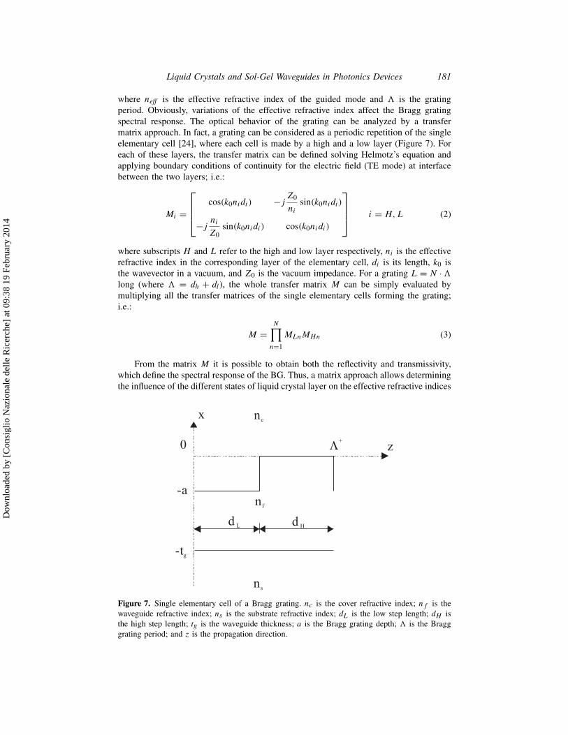
where neff is the effective refractive index of the guided mode and � is the gratingperiod. Obviously, variations of the effective refractive index affect the Bragg gratingspectral response. The optical behavior of the grating can be analyzed by a transfermatrix approach. In fact, a grating can be considered as a periodic repetition of the singleelementary cell [24], where each cell is made by a high and a low layer (Figure 7). Foreach of these layers, the transfer matrix can be defined solving Helmotz’s equation andapplying boundary conditions of continuity for the electric field (TE mode) at interfacebetween the two layers; i.e.:
Mi =
cos(k0nidi) −j Z0
nisin(k0nidi)
−j niZ0
sin(k0nidi) cos(k0nidi)
i = H,L (2)
where subscripts H and L refer to the high and low layer respectively, ni is the effectiverefractive index in the corresponding layer of the elementary cell, di is its length, k0 isthe wavevector in a vacuum, and Z0 is the vacuum impedance. For a grating L = N ·�long (where � = dh + dl), the whole transfer matrix M can be simply evaluated bymultiplying all the transfer matrices of the single elementary cells forming the grating;i.e.:
M =N∏n=1
MLnMHn (3)
From the matrix M it is possible to obtain both the reflectivity and transmissivity,which define the spectral response of the BG. Thus, a matrix approach allows determiningthe influence of the different states of liquid crystal layer on the effective refractive indices
Figure 7. Single elementary cell of a Bragg grating. nc is the cover refractive index; nf is thewaveguide refractive index; ns is the substrate refractive index; dL is the low step length; dH isthe high step length; tg is the waveguide thickness; a is the Bragg grating depth; � is the Bragggrating period; and z is the propagation direction.
Dow
nloa
ded
by [
Con
sigl
io N
azio
nale
del
le R
icer
che]
at 0
9:38
19
Febr
uary
201
4
182 L. Sirleto et al.
of the high and low layers of the elementary cell. In this way, variations on the gratingspectral response due to reorientation of liquid crystal molecules can be evaluated.
According to Eq. (1), any change of the effective refractive index involves a changein the spectral response of the devices. In our devices, the Bragg grating is over-layeredwith a liquid crystal film (Figure 6) and its molecular reorientation can be induced,applying an electrical field between the two ITO electrodes. This reorientation implies achange of the refractive index of the cover of the active region and consequently a changeof the effective refractive index of the guided mode. Therefore, a variation of the Braggwavelength is induced. Thus, if a laser beam propagates along the device, a field-inducedmodulation of the laser intensity at the output of the device can be achieved by a properdesign of the grating period.
In a uniaxial slab, like a uniformly aligned liquid crystal film, a pure phase modu-lation of the incident light is obtained only for the extraordinary wave if the optic axismoves in the plane of incidence. Generally, for example, in bulk Sm-C∗ structures anapplied electric field moves the optic axis out of the polarization plane, resulting in apolarization modulation rather than a phase modulation.
In our geometry, however, the molecules are aligned parallel to the confining glasswaveguide (book-shelf geometry), thus for TE light propagating through the device, with-out an applied electric field, being the light polarization parallel to the plane containingthe optic axis of the liquid crystal over-layer and the propagation direction of light, apure phase modulation can be obtained. Moreover, applying an electric field between thetwo ITO electrodes, the LC molecules tilt in the waveguide plane and so does the opticaxis of the LC over-layer; therefore, a pure modulation is also achieved in this case forTE wave, the polarization state being maintained. As a consequence, the refractive indexexperienced by TE mode is given by the following general relation [6]:
nLC(α) = none√n2o sin2(α)+ n2
e cos2(α)
(4)
where no and ne are the ordinary and extraordinary index respectively and α is the anglebetween the optic axis of the liquid crystal and the direction of propagation of the lightbeam in the waveguide. Therefore, the BG turns the phase modulation into an amplitudemodulation allowing the control of the BG trasmittivity by an electrical driving signal.In this way, the device can be integrated in an optical circuit and can work either asan optical switch or as a continuously tunable frequency filter, depending on the liquidcrystal utilized as a cover.
Integrated Electro-Optical Switch Design
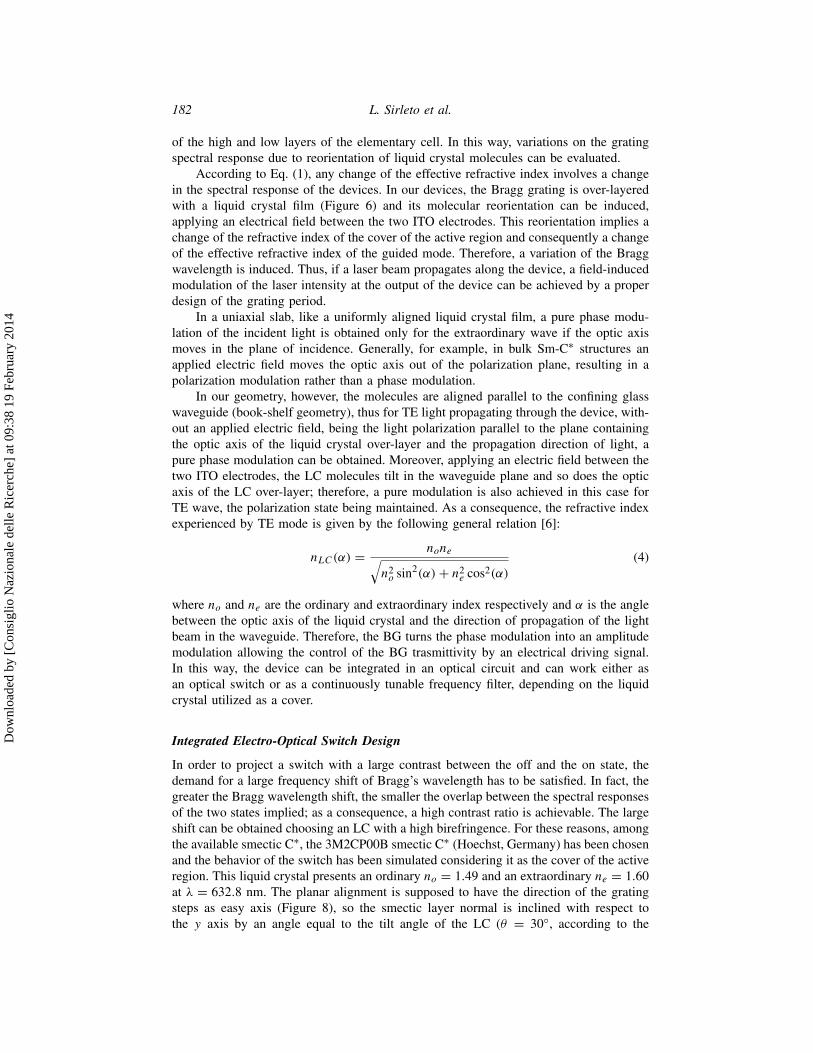
In order to project a switch with a large contrast between the off and the on state, thedemand for a large frequency shift of Bragg’s wavelength has to be satisfied. In fact, thegreater the Bragg wavelength shift, the smaller the overlap between the spectral responsesof the two states implied; as a consequence, a high contrast ratio is achievable. The largeshift can be obtained choosing an LC with a high birefringence. For these reasons, amongthe available smectic C∗, the 3M2CP00B smectic C∗ (Hoechst, Germany) has been chosenand the behavior of the switch has been simulated considering it as the cover of the activeregion. This liquid crystal presents an ordinary no = 1.49 and an extraordinary ne = 1.60at λ = 632.8 nm. The planar alignment is supposed to have the direction of the gratingsteps as easy axis (Figure 8), so the smectic layer normal is inclined with respect tothe y axis by an angle equal to the tilt angle of the LC (θ = 30◦, according to the
Dow
nloa
ded
by [
Con
sigl
io N
azio
nale
del
le R
icer
che]
at 0
9:38
19
Febr
uary
201
4
Liquid Crystals and Sol-Gel Waveguides in Photonics Devices 183
Figure 8. Operating principle of the optical switch. k is the propagation direction of light; Eoptis the field direction of TE mode; +θ is the angle between the smectic layer normal and initialoptic axis orientation of FLC; −θ is the angle between the smectic layer normal and FLC switchedoptic axis orientation; α is the angle between the switched optic axis orientation of FLC and thepropagation direction.
specifications of the data sheet). The waveguide is characterized by a thickness tg = 0.3µm and a refractive index nfilm of 1.650 at the wavelength λ = 632.8 nm.
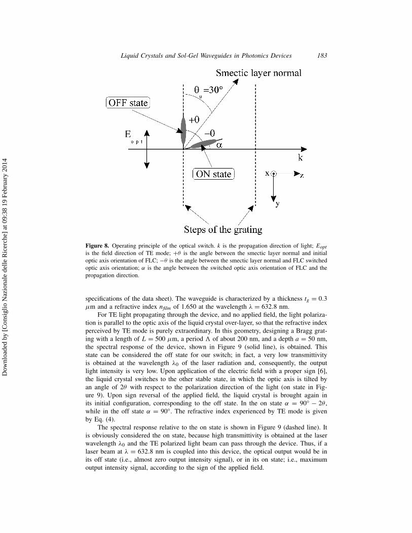
For TE light propagating through the device, and no applied field, the light polariza-tion is parallel to the optic axis of the liquid crystal over-layer, so that the refractive indexperceived by TE mode is purely extraordinary. In this geometry, designing a Bragg grat-ing with a length of L = 500 µm, a period � of about 200 nm, and a depth a = 50 nm,the spectral response of the device, shown in Figure 9 (solid line), is obtained. Thisstate can be considered the off state for our switch; in fact, a very low transmittivityis obtained at the wavelength λ0 of the laser radiation and, consequently, the outputlight intensity is very low. Upon application of the electric field with a proper sign [6],the liquid crystal switches to the other stable state, in which the optic axis is tilted byan angle of 2θ with respect to the polarization direction of the light (on state in Fig-ure 9). Upon sign reversal of the applied field, the liquid crystal is brought again inits initial configuration, corresponding to the off state. In the on state α = 90◦ − 2θ ,while in the off state α = 90◦. The refractive index experienced by TE mode is givenby Eq. (4).
The spectral response relative to the on state is shown in Figure 9 (dashed line). Itis obviously considered the on state, because high transmittivity is obtained at the laserwavelength λ0 and the TE polarized light beam can pass through the device. Thus, if alaser beam at λ = 632.8 nm is coupled into this device, the optical output would be inits off state (i.e., almost zero output intensity signal), or in its on state; i.e., maximumoutput intensity signal, according to the sign of the applied field.
Dow
nloa
ded
by [
Con
sigl
io N
azio
nale
del
le R
icer
che]
at 0
9:38
19
Febr
uary
201
4
184 L. Sirleto et al.
Figure 9. Spectral response of the switch in the off state (solid line) and in the on state (dashedline). $λ is the frequency shift due to the application of the electrical field.
The bandwidth (Figure 9) in the off state is about 2 nm, so no highly coherent sourcesare required for the right working of the optical switch. It is worth noting that the con-traction of the bandwidth in the on state, its bandwidth is of 0.8 nm, and the frequencyshift ($λ = 7 nm), due to the application of the electrical field, guarantees a negligibleoverlap factor between the spectral response of the two states; i.e., a very low theoret-ical crosstalk between channels in an eventual optical communication application. Thisallows obtaining an optical switch with a large contrast between the off and the on state.
Continuously Tunable Filter Design
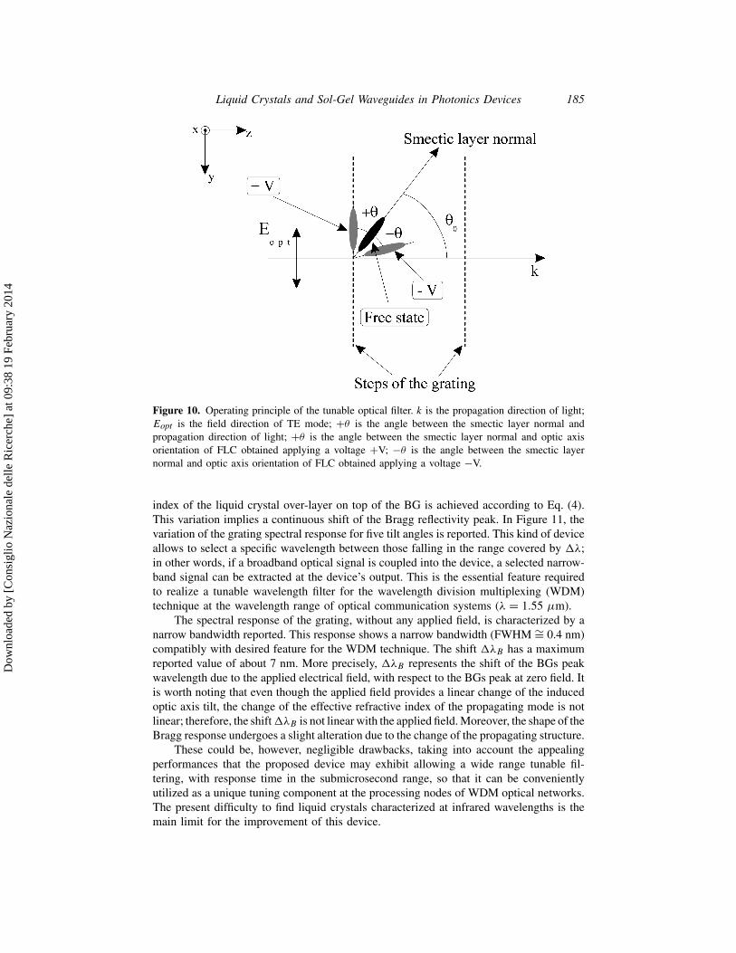
In order to prove our device to be suitable for a wavelength division multiplexing (WDM)application, the previous liquid crystal material is substituted by a commercially availableBDH764E (BDH, Britain), having the ordinary and the extraordinary refractive indexrespectively equal to no = 1.50 and ne = 1.65 at the wavelength λ = 1.55 µm and amaximum value of the tilt angle θmax = 10◦ [25]. Planar alignment with the smecticlayer normal tilted of an angle θmax with respect to the y direction is assumed (free state,in Figure 10).
In order to guarantee the single-mode behavior, the thickness and the refractive indexof the guiding layer are 1.4 µm and 1.67, respectively; moreover, the simulated Bragggrating has a length of 5000 µm and a depth of 50 nm. According to Eq. (1), the periodof the grating is � = 471 nm, which permits the use of less demanding technologicalprocesses compared to the above-mentioned devices working in the visible range.
An applied voltage, continuously varying between Vmax and −Vmax allows obtaininga tilt angle between +θmax and −θmax [25]; hence, a continuous variation of the refractive
Dow
nloa
ded
by [
Con
sigl
io N
azio
nale
del
le R
icer
che]
at 0
9:38
19
Febr
uary
201
4
Liquid Crystals and Sol-Gel Waveguides in Photonics Devices 185
Figure 10. Operating principle of the tunable optical filter. k is the propagation direction of light;Eopt is the field direction of TE mode; +θ is the angle between the smectic layer normal andpropagation direction of light; +θ is the angle between the smectic layer normal and optic axisorientation of FLC obtained applying a voltage +V; −θ is the angle between the smectic layernormal and optic axis orientation of FLC obtained applying a voltage −V.
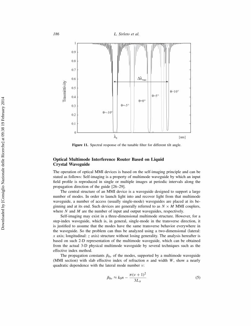
index of the liquid crystal over-layer on top of the BG is achieved according to Eq. (4).This variation implies a continuous shift of the Bragg reflectivity peak. In Figure 11, thevariation of the grating spectral response for five tilt angles is reported. This kind of deviceallows to select a specific wavelength between those falling in the range covered by $λ;in other words, if a broadband optical signal is coupled into the device, a selected narrow-band signal can be extracted at the device’s output. This is the essential feature requiredto realize a tunable wavelength filter for the wavelength division multiplexing (WDM)technique at the wavelength range of optical communication systems (λ = 1.55 µm).
The spectral response of the grating, without any applied field, is characterized by anarrow bandwidth reported. This response shows a narrow bandwidth (FWHM ∼= 0.4 nm)compatibly with desired feature for the WDM technique. The shift $λB has a maximumreported value of about 7 nm. More precisely, $λB represents the shift of the BGs peakwavelength due to the applied electrical field, with respect to the BGs peak at zero field. Itis worth noting that even though the applied field provides a linear change of the inducedoptic axis tilt, the change of the effective refractive index of the propagating mode is notlinear; therefore, the shift$λB is not linear with the applied field. Moreover, the shape of theBragg response undergoes a slight alteration due to the change of the propagating structure.
These could be, however, negligible drawbacks, taking into account the appealingperformances that the proposed device may exhibit allowing a wide range tunable fil-tering, with response time in the submicrosecond range, so that it can be convenientlyutilized as a unique tuning component at the processing nodes of WDM optical networks.The present difficulty to find liquid crystals characterized at infrared wavelengths is themain limit for the improvement of this device.
Dow
nloa
ded
by [
Con
sigl
io N
azio
nale
del
le R
icer
che]
at 0
9:38
19
Febr
uary
201
4
186 L. Sirleto et al.
Figure 11. Spectral response of the tunable filter for different tilt angle.
Optical Multimode Interference Router Based on LiquidCrystal Waveguide
The operation of optical MMI devices is based on the self-imaging principle and can bestated as follows: Self-imaging is a property of multimode waveguide by which an inputfield profile is reproduced in single or multiple images at periodic intervals along thepropagation direction of the guide [26–29].
The central structure of an MMI device is a waveguide designed to support a largenumber of modes. In order to launch light into and recover light from that multimodewaveguide, a number of access (usually single-mode) waveguides are placed at its be-ginning and at its end. Such devices are generally referred to as N ×M MMI couplers,where N and M are the number of input and output waveguides, respectively.
Self-imaging may exist in a three-dimensional multimode structure. However, for astep-index waveguide, which is, in general, single-mode in the transverse direction, itis justified to assume that the modes have the same transverse behavior everywhere inthe waveguide. So the problem can thus be analyzed using a two-dimensional (lateral:x axis; longitudinal: z axis) structure without losing generality. The analysis hereafter isbased on such 2-D representation of the multimode waveguide, which can be obtainedfrom the actual 3-D physical multimode waveguide by several techniques such as theeffective index method.
The propagation constants β0ν of the modes, supported by a multimode waveguide(MMI section) with slab effective index of refraction n and width W , show a nearlyquadratic dependence with the lateral mode number ν:
β0ν ≈ k0n− π(ν + 1)2
3Lπ
(5)
Dow
nloa
ded
by [
Con
sigl
io N
azio
nale
del
le R
icer
che]
at 0
9:38
19
Febr
uary
201
4
Liquid Crystals and Sol-Gel Waveguides in Photonics Devices 187
which follows from k2y + k2
z = k20n
2 with kz = β0ν , ky ≈ (ν+1)πW
, k0 = 2πλ0
, the fact thatβ0ν is close to k0n, and from the definition of beat length Lπ = π
β00−β01[27, 28].
The total lateral profile hy(x, z) at any z position in the MMI section can be writtenas a linear combination of the fields hy,ν(x) of the M guided modes:
hy(x, z) =M−1∑ν=0
cνhy,ν(x) exp(−jβ0νz) (6)
where the coefficients cν determine the relative contribution of each mode. In particular,the total lateral field profile at the entrance (z = 0) of the MMI section is:
hy(x, 0) =M−1∑ν=0
cνhy,ν(x) (7)
which reflects the decomposition of the input field profile into all guided modes.Using the propagation constants given by (5), the total lateral field profile at the end
(z = LMMI ) of the MMI section can be found from
hy(x, LMMI) = exp(−jk0nLMMI)
M−1∑ν=0
cνhy,ν(x) exp
(jπ(ν + 1)2LMMI
3Lπ
)(8)
Inspection of the phase factor leads to the results (Eq. (5)), where q is an integerand the overall phase factor exp(−jk0NLMMI) has been dropped.
hy(x, LMMI) =M−1∑ν=0
cνhy,ν(x) = hy(x, 0) for LMMI = (2q)3Lπ
M−1∑ν=0
(−1)ν+1cνhy,ν(x) = −hy(−x, 0) for LMMI = (2q + 1)3Lπ
j (−1)q + 1
2hy(x, 0)+ j (−1)q − 1
2hy(−x, 0) for LMMI =
(q + 1
2
)3Lπ
(9)
The even and odd symmetry of the modes hy,ν(−x) = (−1)νhy,ν(x) can be used torewrite the previous results in terms of the total lateral field profile at the input. Theseresults show that
when LMMI = (2q)3Lπ , the field at the entrance is reproduced at the end of the MMIsection (self-imaging effect), and the router is in the bar state;
when LMMI = (2q + 1)3Lπ , the field at the end of the MMI section is an y-z planemirror image of the field at the entrance, and the router is in the cross state;
when LMMI = (q+ 12 )3Lπ , the field at the end of the MMI section is a linear combination
of the original field at the entrance and its y-z plane mirror image with a relativephase of π/2. So a two-fold image is obtained (see Figure 12).
Dow
nloa
ded
by [
Con
sigl
io N
azio
nale
del
le R
icer
che]
at 0
9:38
19
Febr
uary
201
4
188 L. Sirleto et al.
Figure 12. Schematic top view of the device.
Working Principle of Device and Numerical Results
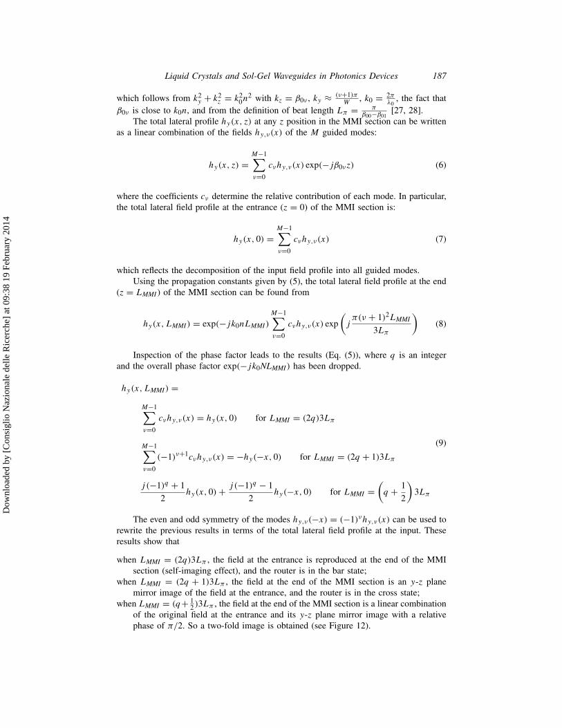
The router is composed of a single-mode input optical channel (rib) waveguide; a bimodalactive region, having a liquid crystal as over-layer; and an output Y branch, to separatethe two output channels. In Figure 13 the structure of device is shown.
The device may be built in silica-titania glass by using a sol-gel deposition [1, 2]on a glass substrate. The refractive index of glass substrate is nsub = 1.516. It is covered
Figure 13. Operating principle of the LC/router.
Dow
nloa
ded
by [
Con
sigl
io N
azio
nale
del
le R
icer
che]
at 0
9:38
19
Febr
uary
201
4
Liquid Crystals and Sol-Gel Waveguides in Photonics Devices 189
with an indium tin oxide (ITO) layer. The thickness and refractive index of the ITO layerare tITO = 20 nm and nITO = 1.9, respectively. The refractive index of the guiding filmis nfilm = 1.670, at the wavelength λ = 1.55 µm. It is worth noting that the thickness ofthe ITO layer has been chosen in order to have negligible effects on the modal behavior[6, 7].
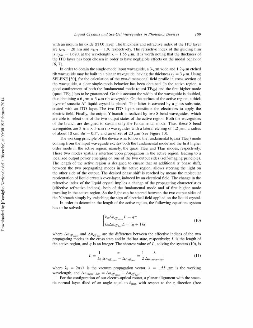
In order to obtain the single-mode input waveguide, a 3-µm wide and 1.2-µm etchedrib waveguide may be built in a planar waveguide, having the thickness tg = 3 µm. UsingSELENE [30], for the calculation of the two-dimensional field profile in cross section ofthe waveguide, a clear single-mode behavior has been obtained. In the active region, agood confinement of both the fundamental mode (quasi TE00) and the first higher mode(quasi TE01) has to be guaranteed. On this account the width of the waveguide is doubled,thus obtaining a 6 µm × 3 µm rib waveguide. On the surface of the active region, a thicklayer of smectic A∗ liquid crystal is placed. This latter is covered by a glass substrate,coated with an ITO layer. The two ITO layers constitute the electrodes to apply theelectric field. Finally, the output Y-branch is realized by two S-bend waveguides, whichare able to select one of the two output states of the active region. Both the waveguidesof the branch are designed to sustain only the fundamental mode. Thus, these S-bendwaveguides are 3 µm × 3 µm rib waveguides with a lateral etching of 1.2 µm, a radiusof about 10 cm, dα = 0.3◦, and an offset of 20 µm (see Figure 13).
The working principle of the device is as follows: the fundamental (quasi TE00) modecoming from the input waveguide excites both the fundamental mode and the first higherorder mode in the active region; namely, the quasi TE00 and TE01 modes, respectively.These two modes spatially interfere upon propagation in the active region, leading to alocalized output power emerging on one of the two output sides (self-imaging principle).The length of the active region is designed to ensure that an additional π phase shift,between the two propagating modes in the active region, allows steering the light onthe other side of the output. The desired phase shift is reached by means the molecularreorientation of liquid crystals over-layer, induced by an electrical field. The change in therefractive index of the liquid crystal implies a change of the propagating characteristics(effective refractive indices), both of the fundamental mode and of first higher modetraveling in the active region. So the light can be steered between the two output sides ofthe Y-branch simply by switching the sign of electrical field applied on the liquid crystal.
In order to determine the length of the active region, the following equations systemhas to be solved: {
k0$neff crossL = qπ
k0$neff barL = (q + 1)π
(10)
where $neff crossand $neff bar
are the difference between the effective indices of the twopropagating modes in the cross state and in the bar state, respectively; L is the length ofthe active region, and q is an integer. The shortest value of L, solving the system (10), is
L = 1
k0
π
$neff cross−$neff bar
= 1
2
λ
$ncross−bar(11)
where k0 = 2π/λ is the vacuum propagation vector, λ = 1.55 µm is the workingwavelength, and $ncross−bar = $neff cross
−$neff bar.
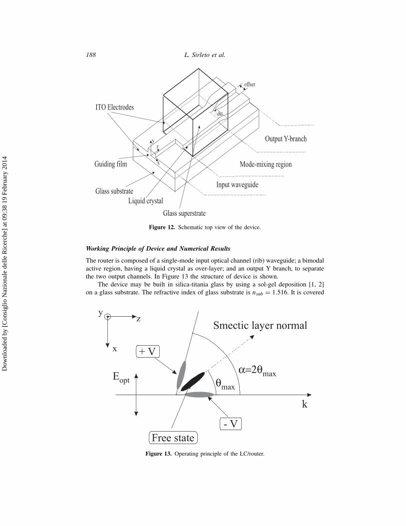
For the configuration of our electro-optical router, a planar alignment with the smec-tic normal layer tilted of an angle equal to θmax with respect to the z direction (free
Dow
nloa
ded
by [
Con
sigl
io N
azio
nale
del
le R
icer
che]
at 0
9:38
19
Febr
uary
201
4
190 L. Sirleto et al.
state in Figure 14) has been supposed. By applying an electric field, the LC moleculestilt in the plane of waveguide (the x-z plane as depicted in Figure 14) letting the anglebetween the average molecular optic axis and the incident beam direction θ to change.In such a way, as the molecules are aligned parallel to the confining glass waveguideand referring to a TE mode as input field, the electro-optic effect turns into a modula-tion of the LC extraordinary refractive index and the output polarization is still linear.
Figure 14. Beam propagation inside the device in cross and bar states.
Dow
nloa
ded
by [
Con
sigl
io N
azio
nale
del
le R
icer
che]
at 0
9:38
19
Febr
uary
201
4
Liquid Crystals and Sol-Gel Waveguides in Photonics Devices 191
In particular, by applying the following voltage values: Vmax and −Vmax, tilt angle +θmaxand −θmax are achieved. As a consequence, the following values for the refractive indexof the liquid crystal over-layer, according to Eq. (4), are obtained: nLC(α = 0) = no ornLC(α = 2 · θmax), depending on the device working condition (the cross and the barstate, respectively).
In order to simulate the router working, a commercially available smectic A∗ liquidcrystal BDH764E has been considered as cover of the active region. This liquid crystalpresents, at wavelength λ = 1.55 µm, an ordinary and an extraordinary refractive indexequal to no = 1.50 and ne = 1.65, respectively, and a maximum value of the tilt angleequal to θmax = 10◦ [25].
As evident from (11), in order to obtain a short optoelectronic device, a maximizationof the difference $ncross−bar = $neff cross
− $neff barhas to be achieved. By means of
SELENE software, simulations for the calculation of the two-dimensional field profile incross sections of the active region have been carried out. In the cross state, according torealized alignment, the supported modes of the active region (TE00 and TE01) experiencethe ordinary refractive index of liquid crystal over-layer, so a $neff cross
= 8.19 · 10−3 hasbeen obtained.
In order to determine the length L of the active region, the $neff for the bar staterelative to a tilt angle of 2 · θmax has to be evaluated. According to Eq. (4), the refractiveindex of the cover of active region is nc = 1.5154 at tilt angle of 20◦. The consequentvariation on the propagating characteristic of the active region involves a $neff bar
=8.08 · 10−3, which established a $ncross−bar
∼= 1.1 · 10−4. Consequently, the length L
needed to guarantee the additional π shift, in order to steer the light on the other side ofthe output Y-branch, is of about 7200 µm. In Figure 14, the spatially interference uponpropagation in the active region is shown in both cross and bar states.
For this device, the crosstalk can be calculated using the following expression:crosstalk (dB) = 10 log10(Pd/Pu), where Pd and Pu are the power on the desiredand on the unwanted output, respectively. For the proposed configuration, a crosstalkof −12.0 dB has been estimated both in cross and bar state.
Conclusions
In this article, a number of integrated electro-optic devices based on hybrid technologycombining liquid crystals and sol-gel waveguide are investigated. We prove that, regardinglight modulation, the most useful active functions such as switching, tunable filtering, andspatial routing, could be figured out. The principal advantages of such devices includepromising performances, fast tuning speed, low power dissipation, low cost, and reduceddimensions.
There are some possible extensions that could be investigated. For example, con-sidering an active stage realized or covered with liquid crystals bounded by two Bragggratings, a Fabry-Perot cavity could be determined. Moreover, the 1 × 2 structure couldbe extended to 1 × N ; in fact, in our analysis we utilize only two possible position ofliquid crystal reorientation, but smectic A∗ enables a continuous reorientation so numbersof position could be considered in order to figure out N out ports.
However, the devices have also some disadvantages. Regarding electro-optical switch-ing and continuously tunable filtering, the experimental realization of Bragg grating andalignment of liquid crystal onto the grating could be an important issue. Regarding opticalmultimode interference router using liquid crystals, the device becomes polarization sen-sitive, so it lost important properties with respect to devices realized with other materials.
Dow
nloa
ded
by [
Con
sigl
io N
azio
nale
del
le R
icer
che]
at 0
9:38
19
Febr
uary
201
4
192 L. Sirleto et al.
References
1. Martellucci, S., A. N. Chester, and M. Bertolotti, Eds. 1994. Advances in Integrated Optics.New York: Kluwer Academic/Plenum Publishers.
2. Najafi, S. I., T. Touam, R. Sara, M. P. Andrews, and M. A. Fardad. 1998. Sol-gel glasswaveguide and grating on silicon. J. Lightw. Tech. 16(9):1640–1646.
3. Walker, D. B., E. N. Glytsis, and T. K. Gaylord. 1996. Ferroelectric liquid crystal wave-guide modulation based on a switchable uniaxial-uniaxial interface. Appl. Optic. 35(16):3016–3030.
4. Alessandro, A. D., and R. Asquini. 2003. Liquid crystal devices for photonic switching appli-cations: State of the art and future developments. Mol. Cryst. Liq. Cryst. 398:207–221.
5. Hermann, D. S., G. Scalia, G. Pitois, F. De Marco, K. D’havé, G. Abbate, M. Lindaren,and A. Hule. 2001. Novel passive polymer waveguides integrated with electro-optically activeferroelectric liquid crystals. Opt. Eng. 40(10):2188–2198.
6. Sirleto, L., D. S. Hermann, G. Sclalia, F. De Marco, L. Komitov, M. Lindgren, P. Mormile,G. C. Righini, and G. Abbate. 2002. Integrated electro-optic switches based on ferroelectricliquid crystal waveguides. Fiber Integrated Optic. 21(4):277–294.
7. Sirleto, L., L. Petti, P. Mormile, G. C. Righini, and G. Abbate. 2002. Fast integrated electro-optical switch and beam deflector based on nematic liquid crystal waveguide. Fiber IntegratedOptic. 21(6):435–450.
8. Sirleto, L., G. Abbate, G. C. Righini, and E. Santamato. 2000. Optical sensors and microsys-tems using liquid crystals. In Optical Sensors and Microsystems New Concepts, MaterialsTechnologies, eds. A. N. Chester, S. Martellucci, and A. G. Mignani, 61–77. New York:Kluwer Academic.
9. Sirleto, L., G. C. Righini, L. Ciaccheri, M. A. Rish, and F. Simoni. 2003. Thermo-optical effectsand fiber optic sensing device based on polymer dispersed liquid crystal. Fiber Integrated Optic.22(1):1–12.
10. Petti, L., L. DeStefano, P. Mormile, G. Abbate, G. C. Righini, and L. Sirleto. 1999. Nonlinearoptical propagation in dye doped liquid crystal waveguide. J. Optic. A: Pure Appl. Optic.1:390–397.
11. Ozaki, M., Y. Sadohara, T. Hatai, and K. Yoshino. 1990. Fast optical switching in polymerwaveguide using ferroelectric liquid crystal. Jpn. J. Appl. Phys. 29:843–845.
12. Sirleto, L., J. W. Klunder, A. Driessen, I. Rendina, and G. Abbate. 2003. Feasibility of an alloptical switch based on cylindrical microresonators and liquid crystals. SPIE 4947:133–140.
13. Clark, N. A., and S. T. Lagerwall. 1980. Submicrosecond bistable electro-optic switching inliquid crystals. Appl. Phys. Lett. 36:899–901.
14. Elston, S. J. 1995. The optic of ferroelectric liquid crystals. J. Mod. Opt. 42(1):19–56.15. Clark, N. A., and S. T. Lagerwall. 1991. Ferroelectric Liquid Crystals: Principles, Properties
and Applications, ed. J. Goodby. Philadelphia: Gordon and Breach.16. Andersson, G., I. Dahl, L. Komitov, S. T. Lagerwall, K. Sharp, and B. Stebler. 1989. Device
physics of the soft mode electro-optic effect. J. Appl. Phys. 66:4983–4995.17. Andersson, G., I. Dahl, P. Keller, W. Kuczynski, S. T. Lagerwall, K. Sharp, and B. Stebler.
1987. Submicrosecond electro-optic switching in the liquid crystal smectic phase: The soft-mode ferroelectric effect. Appl. Phys. 51(9):640–643.
18. Sneh, A., K. M. Johnson, and J. Liu. 1994. High speed analog refractive index modulator thatuses a chiral smectic A∗ liquid crystal. Opt. Lett. 19:305–307.
19. Shani, Y., C. Henry, R. C. Kistler, R. F. Kazarinov, and K. J. Orlowsky. 1991. Integrated opticadiabatic device on silicon. IEEE J. Quant. Electron. 27(31):556–566.
20. Lindgren, S., M. G. Oberg, J. Andre, S. Nilsson, B. Broberg, B. Holmberg, and L. Back-bom. 1992. Loss-compensated optical Y-branch switch in InGaAsP-InP. IEEE J. Lightw. Tech.8(10):1591-1595.
21. de Ridder, R. M., A. F. M. Sander, A. Driessen, and J. H. J. Fluitman. 1993. An integratedoptical adiabatic TE/TM mode splitter on silicon. IEEE J. Lightw. Tech. 11(11):1806–1811.
Dow
nloa
ded
by [
Con
sigl
io N
azio
nale
del
le R
icer
che]
at 0
9:38
19
Febr
uary
201
4
Liquid Crystals and Sol-Gel Waveguides in Photonics Devices 193
22. Lee, C. C., and T. J. Su. 1994. 2 × 2 single-mode 0-gap directional-coupler thermo-opticwaveguide switch on glass. Appl. Optic. 33(30):7016–7022.
23. Yariv, A., and M. Nakamura. 1977. Periodic structures for integrated optics. J. Quant. Electron.13(4):233–253.
24. Winick, K. A. 1992. Effective-index method and coupled theory for almost periodic waveguidegratings: A comparison. Appl. Optic. 31:757–764.
25. Sneh, A., and K. M. Johnson. 1996. High speed continuously tunable liquid crystal filter forWDM networks. J. Lightw. Tech. 14(6):1067–1080.
26. Ulrich, R. 1975. Image formation by phase coincidences in optical waveguides. Optic. Comm.13(3):259–264.
27. Soldano, L. B., and E. C. M. Pennings. 1995. Optical multi-mode interference devices basedon self-imaging: Principle and applications. J. Ligthw. Tech. 13:615–626.
28. Soldano, L. B., F. B. Veermann, M. K. Smit, B. H. Verbeek, A. H. Dubost, and E. C. M.Pennings. 1992. Planar monomode optical couplers based on multimode interference effects.J. Lightw. Tech. 10(12):1843–1850.
29. Besse, P. A., M. Bachmann, H. Melchior, L. B. Soldano, and M. K. Smit. 1994. Opticalbandwidth and fabrication tolerancers of multimode interference couplers. J. Lightw. Tech.12(6):1004–1009.
30. OlympIOs Integrated Optics Software Manual. http://www.c2v.nl
Biographies
Luigi Sirleto received both his degree in physics (with honors) and a Ph.D. inelectronic engineering from the University of Napoli, Italy. From 1995 to 1997 he was inthe Optics and Photonic Department at the Research Institute on Electromagnetic Wave(IROE) of the National Research Council (CNR), Firenze, Italy. From 1998 to 2000,he was in the optoelectronic group of the Electronic Department at the University ofNaples. Since 2001 he has been a researcher at the Institute for Microelectronics andMicrosystems (IMM) of the National Research Council (CNR), Napoli. In September2001 he spent three weeks as visiting scientist at MESA+, University of Twente (NL).From July 2003 to March 2004, as visiting scientist, he was in the OptoelectronicsCircuits and Systems Laboratory at UCLA (University of California, Los Angeles). Hismain fields of interest are optical characterization of material and photonic devices.
Giuseppe Coppola was born in Napoli, Italy, in 1972. He received an M.Sc. inelectronic engineering and a Ph.D. in electronics and computer science in 1997 and2001, respectively, both from the University of Napoli “Federico II.” In 2001 he spentsix months as a visiting scientist at the Delft Institute of Microelectronics and SubmicronTechnologies (Technical University of Delft, The Netherlands), working on the designand realization of an optoelectronic modulator. Since 2002 he has been a researcher at theInstitute for Microelectronics and Microsystems (IMM) of the National Research Council(CNR) in Napoli. His main research interests concern the design and characterization ofsilicon-based optoelectronics devices and characterization of MEMS structures by digitalholography.
Giancarlo C. Righini received a doctorate in physics from Florence University, Italy,in 1967. He is currently the research director at the Research Institute on ElectromagneticWave (IROE) of the National Research Council of Italy (CNR), where he is the head ofthe Optics and Photonics Department. He is a contract professor of optical technologiesat the Specialization School on Optics of the University of Florence. He has more than150 publications in international journals and several book chapters. Dr. Righini has beeneditor of several conference proceedings and is on the editorial board of several journals,
Dow
nloa
ded
by [
Con
sigl
io N
azio
nale
del
le R
icer
che]
at 0
9:38
19
Febr
uary
201
4
194 L. Sirleto et al.
including Optical Materials, Optical Review, Journal of Nonlinear Optical Physics, andMaterials and Photonic Science News. He is a member of the Council of the InternationalUnion of Pure and Applied Physics (IUPAP).
Giancarlo Abbate was born in Naples, Italy, in 1950. He graduated in physics in1973. Since 1985 he was associate professor and since 2001 he has been full professor ofphysics at the University of Naples Federico II. He is the Italian delegate in the PhysicsCommittee of the European COST program, Italian member of the board of directorsof the International Liquid Crystal Society, and coordinator of the European Networkon Liquid Crystal Based Photonic Devices. His scientific interests are in the field ofoptics of liquid crystals and photonic devices. He is the author of about 100 scientificpapers and he has given more than 20 invited presentations at international conferenceson optics. Presently, he coordinates an Italian national project on photonic devices andhe is responsible for the Italian participation (INFM) in several European proposals inthe same field.
Dow
nloa
ded
by [
Con
sigl
io N
azio
nale
del
le R
icer
che]
at 0
9:38
19
Febr
uary
201
4