Solids and Crystals
52
-
Upload
khangminh22 -
Category
Documents
-
view
2 -
download
0
Transcript of Solids and Crystals

Solids and Crystals
1. The nature of binding for a crystal with alternate and evenly spaced positive and negative ions is [CBSE PMT 2000]
(a) Covalent (b) Metallic
(c) Dipolar (d) Ionic
2. For a crystal system, a = b = c, = = 90o, the system is [BHU 2000]
(a) Tetragonal system (b) Cubic system
(c) Orthorhombic system (d) Rhombohedral system
3. Biaxial crystal among the following is [Pb. CET 1998]
(a) Calcite (b) Quartz
(c) Selenite (d) Tourmaline
4. The temperature coefficient of resistance of a conductor is
[AFMC 1998]
(a) Positive always (b) Negative always
(c) Zero (d) Infinite
5. Potassium has a bcc structure with nearest neighbour distance 4.525 Å. Its molecular weight is 39. Its density in kg/m3 is [DCE 1997]
(a) 900 (b) 494
(c) 602 (d) 802
6. The expected energy of the electrons at absolute zero is called [RPET 1996]
(a) Fermi energy (b) Emission energy
(c) Work function (d) Potential energy
7. In a triclinic crystal system [EAMCET (Med.) 1995]
(a) cba , (b) cba ,
(c) cba , (d) cba ,
8. Metallic solids are always opaque because [AFMC 1994]
(a) Solids effect the incident light
(b) Incident light is readily absorbed by the free electron in a metal
(c) Incident light is scattered by solid molecules
(d) Energy band traps the incident light
9. In which of the following ionic bond is present
[EAMCET (Med.) 1994]
(a) NaCl (b) Ar
(c) Si (d) Ge
10. Which of the following materials is non crystalline
[CBSE PMT 1993]
(a) Copper (b) Sodium chloride
(c) Wood (d) Diamond

Electronics 1557
11. The coordination number of Cu is [AMU 1992]
(a) 1 (b) 6
(c) 8 (d) 12
12. Which one of the following is the weakest kind of bonding in solids[CBSE PMT 1992; KCET 1992]
(a) Ionic (b) Metallic
(c) Vander Waals (d) Covalent
13. In a crystal, the atoms are located at the position of
[AMU 1985]
(a) Maximum potential energy
(b) Minimum potential energy
(c) Zero potential energy
(d) Infinite potential energy
14. Crystal structure of NaCl is [NCERT 1982]
(a) Fcc (b) Bcc
(c) Both of the above (d) None of the above
15. What is the coordination number of sodium ions in the case of sodium chloride structure [CBSE PMT 1988]
(a) 6 (b) 8
(c) 4 (d) 12
16. The distance between the body centred atom and a corner atom in
sodium (a = 4.225 Å) is [CBSE PMT 1995]
(a) 3.66 Å (b) 3.17 Å
(c) 2.99 Å (d) 2.54 Å
17. A solid that transmits light in visible region and has a very low
melting point possesses [J & K CET 2001]
(a) Metallic bonding (b) Ionic bonding
(c) Covalent bonding (d) Vander Waal’s bonding
18. Atomic radius of fcc is [J & K CET 2001]
(a) 2
a (b)
22
a
(c) a4
3 (d) a
2
3
19. A solid reflects incident light and it’s electrical conductivity
decreases with temperature. The binding in this solids
(a) Ionic (b) Covalent
(c) Metallic (d) Molecular
20. The laptop PC’s modern electronic watches and calculators use the following for display
(a) Single crystal (b) Poly crystal
(c) Liquid crystal (d) Semiconductors
21. The nearest distance between two atoms in case of a bcc lattice is
equal to [J & K CET 2004]
(a) 3
2a (b)
2
3a
(c) 3q (d) 2
a
22. What is the net force on a Cl– placed at the centre of the bcc
structure of CsCl [DCE 2003; AIIMS 2004]
(a) Zero (b) 22 / ake
(c) 22ake (d) Data is incomplete
23. Sodium has body centred packing. If the distance between two
nearest atoms is 3.7 Å, then its lattice parameter is
[Pb. PET 2002]
(a) 4.8 Å (b) 4.3 Å
(c) 3.9 Å (d) 3.3 Å
24. Which of the following is an amorphous solid
[AIIMS 2005; J & K CET 2004]
(a) Glass (b) Diamond
(c) Salt (d) Sugar
25. Copper has face centered cubic (fcc) lattice with interatomic spacing
equal to 2.54Å. The value of the lattice constant for this lattice is [CBSE PMT 2005]
(a) 1.27 Å (b) 5.08 Å
(c) 2.54 Å (d) 3.59 Å
26. In good conductors of electricity, the type of bonding that exists is [CBSE PMT 1995]
(a) Ionic (b) Vander Waals
(c) Covalent (d) Metallic
27. Bonding in a germanium crystal (semi- conductor) is
[CPMT 1986; KCET 1992; EAMCET (Med.) 1995;
MP PET/PMT 2004]
(a) Metallic (b) Ionic
(c) Vander Waal's type (d) Covalent
28. The ionic bond is absent in [J & K CET 2005]
(a) NaCl (b) CsCl
(c) LiF (d) H2
O
Semiconductors
1. The majority charge carriers in P-type semiconductor are
[MP PMT 1999; CBSE PMT 1999;
MP PET 1991; MP PET/PMT 1998; MH CET 2003]
(a) Electrons (b) Protons
(c) Holes (d) Neutrons
2. A P-type semiconductor can be obtained by adding
[NCERT 1979; BIT 1988; MP PMT 1987; 90]
(a) Arsenic to pure silicon
(b) Gallium to pure silicon
(c) Antimony to pure germanium
(d) Phosphorous to pure germanium
3. The valence of an impurity added to germanium crystal in order to convert it into a P-type semi conductor is
[MP PMT 1989; CPMT 1987]
(a) 6 (b) 5
(c) 4 (d) 3 Cs+ Cs+
Cs+ Cs+
Cs+
Cs+ Cs+
Cs+ Cl
a
a
a

1558 Electronics
4. In a semiconductor, the concentration of electrons is 314 /108 cm and that of the holes is .105 312 cm The
semiconductor is [MP PMT 1997; RPET 1999;
Kerala PET 2002]
(a) P-type (b) N-type
(c) Intrinsic (d) PNP-type
5. In P-type semiconductor, there is [MP PMT 1989]
(a) An excess of one electron
(b) Absence of one electron
(c) A missing atom
(d) A donar level
6. The valence of the impurity atom that is to be added to germanium crystal so as to make it a N-type semiconductor, is
[MNR 1993; MP PET 1994; CBSE PMT 1999; AIIMS 2000]
(a) 6 (b) 5
(c) 4 (d) 3
7. Silicon is a semiconductor. If a small amount of As is added to it, then its electrical conductivity [MP PMT 1996]
(a) Decreases (b) Increases
(c) Remains unchanged (d) Becomes zero
8. When the electrical conductivity of a semi- conductor is due to the breaking of its covalent bonds, then the semiconductor is said to be
[AIIMS 1997; KCET (Engg.) 2002]
(a) Donar (b) Acceptor
(c) Intrinsic (d) Extrinsic
9. A piece of copper and the other of germanium are cooled from the room temperature to 80 K, then which of the following would be a correct statement
[IIT-JEE 1988; Bihar CEE 1992; CBSE PMT 1993; MP PET 1997; RPET 1999; AIEEE 2004]
(a) Resistance of each increases
(b) Resistance of each decreases
(c) Resistance of copper increases while that of germanium decreases
(d) Resistance of copper decreases while that of germanium increases
10. To obtain P-type Si semiconductor, we need to dope pure Si
with [IIT-JEE 1988; MP PET 1997, 93;
Pb. PMT 2001, 02; UPSEAT 2004]
(a) Aluminium (b) Phosphorous
(c) Oxygen (d) Germanium
11. Electrical conductivity of a semiconductor
[MP PMT 1993, 2000; RPET 1996]
(a) Decreases with the rise in its temperature
(b) Increases with the rise in its temperature
(c) Does not change with the rise in its temperature
(d) First increases and then decreases with the rise in its
temperature
12. Three semi-conductors are arranged in the increasing order of their
energy gap as follows. The correct arrangement is
[MP PMT 1993]
(a) Tellurium, germanium, silicon
(b) Tellurium, silicon, germanium
(c) Silicon, germanium, tellurium
(d) Silicon, tellurium, germanium
13. When a semiconductor is heated, its resistance
[KCET 1992; MP PMT 1994; MP PET 1992, 2002;
RPMT 2001; DCE 2001]
(a) Decreases (b) Increases
(c) Remains unchanged (d) Nothing is definite
14. In an insulator, the forbidden energy gap between the valence band
and conduction band is of the order of
[DPMT 1988; EAMCET (Engg.) 1995; MP PET 1996]
(a) MeV1 (b) MeV1.0
(c) eV1 (d) eV5
15. A N-type semiconductor is [AFMC 1988; RPMT 1999]
(a) Negatively charged (b) Positively charged
(c) Neutral (d) None of these
16. The energy band gap of Si is
[MP PET 1994, 2002; BHU 1995; RPMT 2000]
(a) eV70.0
(b) 1.1 eV
(c) Between eV70.0 to eV1.1
(d) 5 eV
17. The forbidden energy band gap in conductors, semiconductors and
insulators are 21 , EGEG and 3EG respectively. The relation
among them is
[MP PMT 1994; RPMT 1997]
(a) 321 EGEGEG (b) 321 EGEGEG
(c) 321 EGEGEG (d) 321 EGEGEG
18. Which statement is correct [MP PMT 1994]
(a) N-type germanium is negatively charged and P-type germanium
is positively charged
(b) Both N-type and P-type germanium are neutral
(c) N-type germanium is positively charged and P-type germanium
is negatively charged
(d) Both N-type and P-type germanium are negatively charged
19. When Ge crystals are doped with phosphorus atom, then it becomes [AFMC 1995; Orissa PMT 2004]
(a) Insulator (b) P-type
(c) N-type (d) Superconductor
20. Let Pn and en be the number of holes and conduction electrons
respectively in a semiconductor. Then
[MP PET 1995]
(a) eP nn in an intrinsic semiconductor
(b) eP nn in an extrinsic semiconductor
(c) eP nn in an intrinsic semiconductor
(d) Pe nn in an intrinsic semiconductor

Electronics 1559
21. Wires P and Q have the same resistance at ordinary (room)
temperature. When heated, resistance of P increases and that of Q
decreases. We conclude that
[MP PMT 1995; MP PET 2001]
(a) P and Q are conductors of different materials
(b) P is N-type semiconductor and Q is P-type semiconductor
(c) P is semiconductor and Q is conductor
(d) P is conductor and Q is semiconductor
22. The impurity atoms which are mixed with pure silicon to make a P-type semiconductor are those of [MP PMT 1995]
(a) Phosphorus (b) Boron
(c) Antimony (d) Copper
23. Holes are charge carriers in [IIT-JEE 1996]
(a) Intrinsic semiconductors (b) Ionic solids
(c) P-type semiconductors (d) Metals
24. In extrinsic P and N-type, semiconductor materials, the ratio of the
impurity atoms to the pure semiconductor atoms is about [MP PET 2003]
(a) 1 (b) 110
(c) 410 (d) 710
25. A hole in a P-type semiconductor is [MP PET 1996]
(a) An excess electron (b) A missing electron
(c) A missing atom (d) A donor level
26. The forbidden gap in the energy bands of germanium at room temperature is about [MP PMT/PET 1998]
(a) eV1.1 (b) eV1.0
(c) eV67.0 (d) eV7.6
27. In P-type semiconductor the majority and minority charge carriers are respectively
[EAMCET 1994; MP PMT/PET 1998; MH CET 2000]
(a) Protons and electrons (b) Electrons and protons
(c) Electrons and holes (d) Holes and electrons
28. At zero Kelvin a piece of germanium [MP PET 1999]
(a) Becomes semiconductor
(b) Becomes good conductor
(c) Becomes bad conductor
(d) Has maximum conductivity
29. Electronic configuration of germanium is 2, 8, 18 and 4. To make it extrinsic semiconductor small quantity of antimony is added [MP PET 1999]
(a) The material obtained will be N-type germanium in which electrons and holes are equal in number
(b) The material obtained will be P-type germanium
(c) The material obtained will be N-type germanium which has more electrons than holes at room temperature
(d) The material obtained will be N-type germanium which has less electrons than holes at room temperature
30. A semiconductor is cooled from KT1 to .2 KT Its resistance
[MP PET 1999]
(a) Will decrease
(b) Will increase
(c) Will first decrease and then increase
(d) Will not change
31. If PN and eN be the numbers of holes and conduction electrons in
an extrinsic semiconductor, then
[MP PMT 1999; AMU 2001]
(a) eP NN
(b) eP NN
(c) eP NN
(d) eP NN or eP NN depending on the nature of impurity
32. In intrinsic semiconductor at room temperature, number of electrons and holes are
[EAMCET (Engg.) 1995; JIPMER 2001, 02]
(a) Equal (b) Zero
(c) Unequal (d) Infinite
33. (USS 133) Indium impurity in germanium makes
[EAMCET (Engg.) 1995]
(a) N-type (b) P-type
(c) Insulator (d) Intrinsic
34. Fermi level of energy of an intrinsic semiconductor lies
[EAMCET (Med.) 1995]
(a) In the middle of forbidden gap
(b) Below the middle of forbidden gap
(c) Above the middle of forbidden gap
(d) Outside the forbidden gap
35. In a semiconductor the separation between conduction band and valence band is of the order of
[EAMCET (Med.) 1995; AIIMS 2000]
(a) eV100 (b) eV10
(c) eV1 (d) 0 eV
36. The intrinsic semiconductor becomes an insulator at
[EAMCET (Med.) 1995; KCET (Engg./Med.) 1999;
MP PET 2000; CBSE PMT 2001]
(a) C0 (b) C100
(c) K300 (d) K0
37. The addition of antimony atoms to a sample of intrinsic germanium transforms it to a material which is
[AMU 1995]
(a) Superconductor (b) An insulator
(c) N-type semiconductor (d) P-type semiconductor
38. Resistance of semiconductor at K0 is [RPET 1997]
(a) Zero (b) Infinite
(c) Large (d) Small
39. In a good conductor the energy gap between the conduction band and the valence band is
[KCET 1993; EMCET (Med.) 1994]
(a) Infinite (b) Wide
(c) Narrow (d) Zero
40. The impurity atom added to germanium to make it N-type
semiconductor is [KCET 1993; KCET (Engg./Med.) 2000]

1560 Electronics
(a) Arsenic (b) Iridium
(c) Aluminium (d) Iodine
41. When N-type of semiconductor is heated
[CBSE PMT 1993; DPMT 2000]
(a) Number of electrons increases while that of holes decreases
(b) Number of holes increases while that of electrons decreases
(c) Number of electrons and holes remains same
(d) Number of electrons and holes increases equally
42. To obtain a P-type germanium semiconductor, it must be doped with [CBSE PMT 1997; Pb. PET 2000]
(a) Arsenic (b) Antimony
(c) Indium (d) Phosphorus
43. The temperature coefficient of resistance of a semiconductor
[AFMC 1998, MNR 1998]
(a) Is always positive
(b) Is always negative
(c) Is zero
(d) May be positive or negative or zero
44. P-type semiconductor is formed when [RPET 1999]
A. As impurity is mixed in Si
B. Al impurity is mixed in Si
C. B impurity is mixed in Ge
D. P impurity is mixed in Ge
(a) A and C (b) A and D
(c) B and C (d) B and D
45. In case of a semiconductor, which of the following statement is wrong [Pb. PMT 1999]
(a) Doping increases conductivity
(b) Temperature coefficient of resistance is negative
(c) Resisitivity is in between that of a conductor and insulator
(d) At absolute zero temperature, it behaves like a conductor
46. Energy bands in solids are a consequence of
[DCE 1999, 2000; AIEEE 2004]
(a) Ohm’s Law
(b) Pauli’s exclusion principle
(c) Bohr’s theory
(d) Heisenberg’s uncertainty principle
47. In a P-type semiconductor
[AIIMS 1997; Orissa JEE 2002; MP PET 2003]
(a) Current is mainly carried by holes
(b) Current is mainly carried by electrons
(c) The material is always positively charged
(d) Doping is done by pentavalent material
48. At ordinary temperatures, the electrical conductivity of semi
conductors in r/metemho is in the range [MP PET 2003]
(a) 310 to 410 (b) 610 to 910
(c) 610 to 1010 (d) 1010 to 1610
49. When the temperature of silicon sample is increased from C27 to
C100 , the conductivity of silicon will be
[RPMT 1999]
(a) Increased (b) Decreased
(c) Remain same (d) Zero
50. In a P-type semiconductor, germanium is doped with
[AFMC 1999]
(a) Boron (b) Gallium
(c) Aluminium (d) All of these
51. In N-type semiconductors, majority charge carriers are
[AIIMS 1999]
(a) Holes (b) Protons
(c) Neutrons (d) Electrons
52. Semiconductor is damaged by the strong current due to
[MH CET 2000]
(a) Lack of free electron (b) Excess of electrons
(c) Excess of proton (d) None of these
53. GaAs is [RPMT 2000]
(a) Element semiconductor
(b) Alloy semiconductor
(c) Bad conductor
(d) Metallic semiconductor
54. If en and hn are the number of electrons and holes in a
semiconductor heavily doped with phosphorus, then
[MP PMT 2000]
(a) he nn (b) he nn
(c) he nn (d) he nn
55. An N-type and P-type silicon can be obtained by doping pure silicon
with [EAMCET (Med.) 2000]
(a) Arsenic and Phosphorous (b) Indium and Aluminium
(c) Phosphorous and Indium (d) Aluminium and Boron
56. N-type semiconductors will be obtained, when germanium is doped
with [AIIMS 2000]
(a) Phosphorus (b) Aluminium
(c) Arsenic (d) Both (a) or (c)
57. The state of the energy gained by valance electrons when the temperature is raised or when electric field is applied is called as [CBSE PMT 2000]
(a) Valance band (b) Conduction band
(c) Forbidden band (d) None of these
58. To obtain electrons as majority charge carriers in a semiconductor,
the impurity mixed is [MP PET 2000]
(a) Monovalent (b) Divalent
(c) Trivalent (d) Pentavalent
59. For germanium crystal, the forbidden energy gap in joules is
[MP PET 2000]
(a) 191012.1 (b) 191076.1
(c) 19106.1 (d) Zero
60. A pure semiconductor behaves slightly as a conductor at
[MH CET (Med.) 2001; BHU 2000; AFMC 2001]
(a) Room temperature (b) Low temperature

Electronics 1561
(c) High temperature (d) Both (b) and (c)
61. Which is the correct relation for forbidden energy gap in conductor,
semi conductor and insulator
[RPMT 2001; AIEEE 2002]
(a) insulatorscc EgEgEg
(b) conductorscinsulator EgEgEg
(c) scinsulatorconductor EgEgEg
(d) insulatorconductorsc EgEgEg
62. The band gap in Germanium and silicon in eV respectively is [MP PMT 2001]
(a) 0.7, 1.1 (b) 1.1, 0.7
(c) 1.1, 0 (d) 0, 1.1
63. P-type semiconductors are made by adding impurity element [MP PMT 2001]
(a) As (b) P
(c) B (d) Bi
64. At room temperature, a P-type semiconductor has
[Kerala PMT 2002]
(a) Large number of holes and few electrons
(b) Large number of free electrons and few holes
(c) Equal number of free electrons and holes
(d) No electrons or holes
65. In intrinsic semiconductor at room temperature, number of
electrons and holes are [JIPMER 2001, 02; MP PMT 2002]
(a) Unequal (b) Equal
(c) Infinite (d) Zero
66. The valence band and conduction band of a solid overlap at low
temperature, the solid may be
[Orissa JEE 2002; BCECE 2004]
(a) A metal (b) A semiconductor
(c) An insulator (d) None of these
67. Which impurity is doped in Si to form N-type semi-conductor?[CBSE PMT 1996; AIEEE 2002]
(a) Al (b) B
(c) As (d) None of these
68. In a semiconductor [AIEEE 2002; AIIMS 2002]
(a) There are no free electrons at any temperature
(b) The number of free electrons is more than that in a conductor
(c) There are no free electrons at 0 K
(d) None of these
69. The energy band gap is maximum in [AIEEE 2002]
(a) Metals (b) Superconductors
(c) Insulators (d) Semiconductors
70. The process of adding impurities to the pure semiconductor is called
[MH CET 2002]
(a) Drouping (b) Drooping
(c) Doping (d) None of these
71. When phosphorus and antimony are mixed in zermaniun, then [CPMT 2003]
(a) P-type semiconductor is formed
(b) N-type semiconductor is formed
(c) Both (a) and (b)
(d) None of these
72. To a germanium sample, traces of gallium are added as an impurity.
The resultant sample would behave like
[AIIMS 2003]
(a) A conductor
(b) A P-type semiconductor
(c) An N-type semiconductor
(d) An insulator
73. For non-conductors, the energy gap is
[EAMCET (Engg.) 1995; MP PET 1996; RPET 2003]
(a) 6 eV (b) 1.1 eV
(c) 0.8 eV (d) 0.3 eV
74. Donor type impurity is found in [RPET 2003]
(a) Trivalent elements (b) Pentavalent elements
(c) In both the above (d) None of these
75. The difference in the variation of resistance with temperature in a
metal and a semiconductor arises essentially due to the difference in
the [AIEEE 2003]
(a) Variation of scattering mechanism with temperature
(b) Crystal structure
(c) Variation of the number of charge carriers with temperature
(d) Type of bon
76. The charge on a hole is equal to the charge of
[MP PMT 2004]
(a) Zero (b) Proton
(c) Neutron (d) Electron
77. When germanium is doped with phosphorus, the doped material has [MP PMT 2004]
(a) Excess positive charge
(b) Excess negative charge
(c) More negative current carriers
(d) More positive current carriers
78. A Ge specimen is doped with Al. The concentration of acceptor
atoms is ~1021 atoms/m3. Given that the intrinsic concentration of
electron hole pairs is 319 /10~ m , the concentration of electrons
in the specimen is [AIIMS 2004]
(a) 317 /10 m (b) 315 /10 m
(c) 34 /10 m (d) 32 /10 m
79. Which of the following has negative temperature coefficient of
resistance [AFMC 2004]
(a) Copper (b) Aluminium
(c) Iron (d) Germanium
80. In semiconductors at a room temperature [CBSE PMT 2004]
(a) The valence band is partially empty and the conduction band is
partially filled

1562 Electronics
(b) The valence band is completely filled and the conduction band is partially filled
(c) The valence band is completely filled
(d) The conduction band is completely empty
81. Regarding a semiconductor which one of the following is wrong [CPMT 2004]
(a) There are no free electrons at room temperature
(b) There are no free electrons at 0 K
(c) The number of free electrons increases with rise of
temperature
(d) The charge carriers are electrons and holes
82. Which of the following statements is true for an N-type semi-
conductor [CPMT 2004]
(a) The donor level lies closely below the bottom of the conduction
band
(b) The donor level lies closely above the top of the valence band
(c) The donor level lies at the halfway mark of the forbidden energy gap
(d) None of above
83. Choose the correct statement [DCE 2004]
(a) When we heat a semiconductor its resistance increases
(b) When we heat a semiconductor its resistance decreases
(c) When we cool a semiconductor to 0 K then it becomes super conductor
(d) Resistance of a semiconductor is independent of temperature
84. In a P-type semi-conductor, germanium is dopped with
[MH CET 2003]
(a) Gallium (b) Boron
(c) Aluminium (d) All of these
85. A piece of semiconductor is connected in series in an electric circuit.
On increasing the temperature, the current in the circuit will [RPMT 2003]
(a) Decrease (b) Remain unchanged
(c) Increase (d) Stop flowing
86. Intrinsic semiconductor is electrically neutral. Extrinsic
semiconductor having large number of current carriers would be [AMU (Engg.) 2001]
(a) Positively charged
(b) Negatively charged
(c) Positively charged or negatively charged depending upon the
type of impurity that has been added
(d) Electrically neutral
87. If ne
and vd
be the number of electrons and drift velocity in a
semiconductor. When the temperature is increased
[Pb. CET 2000]
(a) ne
increases and vd
decreases
(b) ne
decreases and vd
increases
(c) Both ne
and vd
increases
(d) Both ne
and vd
decreases
88. In extrinsic semiconductors [EAMCET (Engg.) 1999]
(a) The conduction band and valence band overlap
(b) The gap between conduction band and valence band is more
than 16 eV
(c) The gap between conduction band and valence band is near
about 1 eV
(d) The gap between conduction band and valence band will be 100
eV and more
89. Resistivity of a semiconductor depends on [MP PMT 1999]
(a) Shape of semiconductor
(b) Atomic nature of semiconductor
(c) Length of semiconductor
(d) Shape and atomic nature of semiconductor
90. Electric current is due to drift of electrons in [CPMT 1996]
(a) Metallic conductors
(b) Semi-conductors
(c) Both (a) and (b)
(d) None of these
91. The energy gap of silicon is 1.14 eV. The maximum wavelength at which silicon will begin absorbing energy is
[MP PMT 1993]
(a) 10888 Å (b) 1088.8 Å
(c) 108.88 Å (d) 10.888 Å
92. Which of the following energy band diagram shows the N-type
semiconductor [RPET 1986]
(a) (b)
(c) (d)
93. The mobility of free electron is greater than that of free holes
because
(a) The carry negative charge
(b) They are light
(c) They mutually collide less
(d) They require low energy to continue their motion
94. The relation between the number of free electrons in
semiconductors (n) and its temperature (T) is
(a) 2Tn (b) Tn
(c) Tn (d) 2/3Tn
Eg 1eV
Conduction
band (CB)
Valance band (VB)
1eV
Conduction
band (CB)
Valance band (VB)
Impurity
level
1eV
Valance band (VB)
Conduction band (CB)
Impurity
level 1eV
Valance
band (VB)
Conduction band (CB)

95. The electron mobility in N-type germanium is 3900 cm2/v-s and its
conductivity is 6.24 mho/cm, then impurity concentration will be if
the effect of cotters is negligible
(a) 1015 cm
3
(b) 1013 /cm3
(c) 1012 /cm3 (d) 1016 /cm3
96. Which of the energy band diagrams shown in the figure corresponds
to that of a semiconductor [Orissa JEE 2003]
(a) (b)
(c) (d)
97. The energy band diagrams for three semiconductor samples of silicon are as shown. We can then assert that
[Haryana CEE 1996]
(a) Sample X is undoped while samples Y and Z have been doped with a third group and a fifth group impurity respectively
(b) Sample X is undoped while both samples Y and Z have been doped with a fifth group impurity
(c) Sample X has been doped with equal amounts of third and fifth group impurities while samples Y and Z are undoped
(d) Sample X is undoped while samples Y and Z have been doped with a fifth group and a third group impurity respectively
98. Carbon, silicon and Germanium atoms have four valence electrons each. Their valence and conduction band are separated by energy band gaps represented by (E
g
)C
. (Eg
)Si
and (Eg
)Ge
respectively. Which one of the following relationship is true in their case [CBSE PMT 2005]
99. A semiconductor dopped with a donor impurity is
[AFMC 2005]
(a) P-type (b) N-type
(c) NPN type (d) PNP type
100. In a semiconducting material the mobilities of electrons and holes
are e
and h
respectively. Which of the following is true [AIIMS 2005]
101. Doping of intrinsic semiconductor is done [Orissa JEE 2005]
(a) To neutralize charge carriers
(b) To increase the concentration of majority charge carriers
(c) To make it neutral before disposal
(d) To carry out further purification
Semiconductor Diode
1. In the forward bias arrangement of a PN-junction diode
[MP PMT 1994, 96, 99]
(a) The N-end is connected to the positive terminal of the battery
(b) The P-end is connected to the positive terminal of the battery
(c) The direction of current is from N-end to P-end in the diode
(d) The P-end is connected to the negative terminal of battery
2. In a PN-junction diode [MP PET 1993]
(a) The current in the reverse biased condition is generally very small
(b) The current in the reverse biased condition is small but the forward biased current is independent of the bias voltage
(c) The reverse biased current is strongly dependent on the applied bias voltage
(d) The forward biased current is very small in comparison to
reverse biased current
3. The cut-in voltage for silicon diode is approximately
(a) 0.2 V (b) 0.6 V
(c) 1.1 V (d) 1.4 V
circuit is called [KCET 2003]
(a) Oscillator (b) Filter
(c) Amplifier (d) Logic gates
5. PN-junction diode works as a insulator, if connected
[CPMT 1987]
(a) To A.C. (b) In forward bias
(c) In reverse bias (d) None of these
6. The reverse biasing in a PN junction diode
[MP PMT 1991; EAMCET 1994; CBSE PMT 2003]
(a) Decreases the potential barrier
(b) Increases the potential barrier
(c) Increases the number of minority charge carriers
(d) Increases the number of majority charge carriers
7. The electrical resistance of depletion layer is large because
(a) It has no charge carriers
(b) It has a large number of charge carriers
(c) It contains electrons as charge carriers
(d) It has holes as charge carriers
8. In the circuit given below, the value of the current is
9. What is the current in the circuit shown below
[AFMC 2000; RPMT 2001]
X Y Z
CB
VB
CB
VB
CB
Eg >> KT VB
CB
VB Eg = KT
– 4V PN 300 – 1V
+ 4V P N 300 + 1V
(c) 210 amp (d) 310 amp
(a) 0 amp (b) 210 amp
4. The electrical circuit used to get smooth dc output from a rectifier
(d) 0;0 he
(c) he
(b) he(a) he
(a) SigCg EE )()( (b) SigCg EE )()(
(c) GegCg EE )()( (d) SigCg EE )()(
(a) 0 amp (b) 102 amp
(c) 1 amp (d) 0.10 amp

Electronics 1565
10. If the forward voltage in a semiconductor diode is doubled, the
width of the depletion layer will [MP PMT 1996]
(a) Become half (b) Become one-fourth
(c) Remain unchanged (d) Become double
11. The PN junction diode is used as
[CPMT 1972; AFMC 1997; CBSE PMT 1999;
AIIMS 1999; RPMT 2000; MP PMT 04]
(a) An amplifier (b) A rectifier
(c) An oscillator (d) A modulator
12. When a PN junction diode is reverse biased
(a) Electrons and holes are attracted towards each other and move
towards the depletion region
(b) Electrons and holes move away from the junction depletion
region
(c) Height of the potential barrier decreases
(d) No change in the current takes place
13. Two PN-junctions can be connected in series by three different
methods as shown in the figure. If the potential difference in the
junctions is the same, then the correct connections will be [IIT-JEE 1989]
(a) In the circuit (1) and (2) (b) In the circuit (2) and (3)
(c) In the circuit (1) and (3) (d) Only in the circuit (1)
14. A PN- junction has a thickness of the order of [BIT 1990]
(a) cm1 (b) mm1
(c) m610 (d) cm1210
15. In the depletion region of an unbiased P-N junction diode there are [KCET 1999; CBSE PMT 1999;
RPMT 2001; MP PMT 1994, 2003]
(a) Only electrons
(b) Only holes
(c) Both electrons and holes
(d) Only fixed ions
16. On increasing the reverse bias to a large value in a PN-junction
diode, current [MP PMT 1994; BHU 2002]
(a) Increases slowly (b) Remains fixed
(c) Suddenly increases (d) Decreases slowly
17. In the case of forward biasing of PN-junction, which one of the following figures correctly depicts the direction of flow of carriers [CBSE PMT 1995]
(a) (b)
(c) (d)
18. Which of the following statements concerning the depletion zone of an unbiased PN junction is (are) true
[IIT-JEE 1995]
(a) The width of the zone is independent of the densities of the dopants (impurities)
(b) The width of the zone is dependent on the densities of the dopants
(c) The electric field in the zone is produced by the ionized dopant atoms
(d) The electric field in the zone is provided by the electrons in the conduction band and the holes in the valence band
19. A semiconductor device is connected in a series circuit with a battery and a resistance. A current is found to pass through the circuit. If the polarity of the battery is reversed, the current drops almost to zero. The device may be
[MP PET 1995; CBSE PMT 1998]
(a) A P-type semiconductor (b) An N-type semiconductor
(c) A PN-junction (d) An intrinsic semiconductor
20. The approximate ratio of resistances in the forward and reverse bias
of the PN-junction diode is
[MP PET 2000; MP PMT 1999, 2002, 03; Pb. PMT 2003]
(a) 1:10 2 (b) 1:10 2
(c) 410:1 (d) 410:1
21. In a junction diode, the holes are due to
[CBSE PMT 1999; Pb. PMT 2003]
(a) Protons (b) Neutrons
(c) Extra electrons (d) Missing of electrons
22. In forward bias, the width of potential barrier in a P-N junction
diode [EAMCET (Engg.) 1995; CBSE PMT 1999
RPMT 1997, 2002, 03]
(a) Increases
(b) Decreases
(c) Remains constant
(d) First increases then decreases
23. The cause of the potential barrier in a P-N diode is
[CBSE PMT 1998; RPMT 2001]
(a) Depletion of positive charges near the junction
(b) Concentration of positive charges near the junction
(c) Depletion of negative charges near the junction
(d) Concentration of positive and negative charges near the
junction
24. In a PN-junction diode not connected to any circuit
[IIT-JEE 1998]
(a) The potential is the same everywhere
(b) The P-type is a higher potential than the N-type side
(c) There is an electric field at the junction directed from the N-
type side to the P- type side
P N N P
+ –
P N P N
+ –
N P N P
+ –
1 2 3
N
Vp
+ +
+
+ +
P
– –
–
– –
N
Vp
+ +
+
+ +
P
– –
–
– –
N
Vp
+ +
+
+ +
P
– –
–
– –
N
Vp
+ +
+
+ +
P
– –
–
– –

1566 Electronics
(d) There is an electric field at the junction directed from the P-
type side to the N-type side
25. Which of the following statements is not true
[IIT-JEE 1997 Re-Exam]
(a) The resistance of intrinsic semiconductors decrease with
increase of temperature
(b) Doping pure Si with trivalent impurities give P-type
semiconductors
(c) The majority carriers in N-type semiconductors are
holes
(d) A PN-junction can act as a semiconductor diode
26. The dominant mechanisms for motion of charge carriers in forward
and reverse biased silicon P-N junctions are
[IIT-JEE 1997 Cancelled; RPMT 2000; AIIMS 2000]
(a) Drift in forward bias, diffusion in reverse bias
(b) Diffusion in forward bias, drift in reverse bias
(c) Diffusion in both forward and reverse bias
(d) Drift in both forward and reverse bias
27. In P-N junction, avalanche current flows in circuit when biasing is [RPET 1997]
(a) Forward (b) Reverse
(c) Zero (d) Excess
28. The depletion layer in the P-N junction region is caused by
[CBSE PMT 1994]
(a) Drift of holes
(b) Diffusion of charge carriers
(c) Migration of impurity ions
(d) Drift of electrons
29. Which one is reverse-biased [DCE 1999]
(a) (b)
(c) (d)
30. In a P-N junction diode if P region is heavily doped than n region
then the depletion layer is [RPMT 1999]
(a) Greater in P region
(b) Greater in N region
(c) Equal in both region
(d) No depletion layer is formed in this case
31. Which one is in forward bias [RPMT 2000]
(a) (b)
(c) (d) None of these
32. The reason of current flow in P-N junction in forward bias is
[RPMT 2000]
(a) Drifting of charge carriers
(b) Minority charge carriers
(c) Diffusion of charge carriers
(d) All of these
33. The resistance of a reverse biased P-N junction diode is about [MP PMT 2000]
(a) 1 ohm (b) 210 ohm
(c) 310 ohm (d) 610 ohm
34. Consider the following statements A and B and identify the correct
choice of the given answers
A: The width of the depletion layer in a P-N junction diode increases
in forwards bias
B: In an intrinsic semiconductor the fermi energy level is exactly
in the middle of the forbidden gap
[EAMCET (Engg.) 2000]
(a) A is true and B is false (b) Both A and B are false
(c) A is false and B is true (d) Both A and B are true
35. In comparison to a half wave rectifier, the full wave rectifier gives
lower [AFMC 2001]
(a) Efficiency (b) Average dc
(c) Average output voltage (d) None of these
36. Avalanche breakdown is due to [RPMT 2001]
(a) Collision of minority charge carrier
(b) Increase in depletion layer thickness
(c) Decrease in depletion layer thickness
(d) None of these
37. Which is reverse biased diode [DCE 2001]
(a) (b)
(c) (d)
38. Zener breakdown in a semi-conductor diode occurs when
[UPSEAT 2002]
(a) Forward current exceeds certain value
(b) Reverse bias exceeds certain value
(c) Forward bias exceeds certain value
(d) Potential barrier is reduced to zero
39. When forward bias is applied to a P-N junction, then what happens
to the potential barrier BV , and the width of charge depleted
region x [UPSEAT 2002, 03;
Roorkee 1999; RPET 2003; AIEEE 2004]
(a) BV increases, x decreases
(b) BV decreases, x increases
(c) BV increases, x increases
(d) BV decreases, x decreases
+ –
10V 15V
– 10V
– 10V
– 5V
10V
– 5V
–10V
–20V
5V
10V
15V
– 5V
10V
+ –

Electronics 1567
40. The potential barrier, in the depletion layer, is due to
[EAMCET (Engg.) 1998;
Pb. PMT 1999; Pb. PET 2001; AIIMS 2002]
(a) Ions (b) Holes
(c) Electrons (d) Both (b) and (c)
41. In the given figure, which of the diodes are forward biased ?
[Kerala PET 2002]
1. 2.
3. 4.
5.
(a) 1, 2, 3 (b) 2, 4, 5
(c) 1, 3, 4 (d) 2, 3, 4
42. Function of rectifier is [AFMC 2002, 04]
(a) To convert ac into dc (b) To convert dc into ac
(c) Both (a) and (b) (d) None of these
43. When the P end of P-N junction is connected to the negative terminal of the battery and the N end to the positive terminal of the battery, then the P-N junction behaves like [MP PET 2002]
(a) A conductor (b) An insulator
(c) A super-conductor (d) A semi-conductor
44. If the two ends P and N of a P-N diode junction are joined by a wire [MP PMT 2002]
(a) There will not be a steady current in the circuit
(b) There will be a steady current from N side to P side
(c) There will be a steady current from P side to N side
(d) There may not be a current depending upon the resistance of the connecting wire
45. A potential barrier of 0.50 V exists across a P-N junction. If the
depletion region is 7100.5 m wide, the intensity of the electric
field in this region is [UPSEAT 2002]
(a) mV/100.1 6 (b) mV/100.1 5
(c) mV/100.2 5 (d) mV/100.2 6
46. If no external voltage is applied across P-N junction, there would be [Orissa JEE 2002]
(a) No electric field across the junction
(b) An electric field pointing from N-type to P-type side across the junction
(c) An electric field pointing from P-type to N-type side across the
junction
(d) A temporary electric field during formation of P-N junction
that would subsequently disappear
47. In a PN-junction [CBSE PMT 2002]
(a) P and N both are at same potential
(b) High potential at N side and low potential at P side
(c) High potential at P side and low potential at N side
(d) Low potential at N side and zero potential at P side
48. For the given circuit of PN-junction diode, which of the following
statement is correct [CBSE PMT 2002]
(a) In forward biasing the voltage across R is V
(b) In forward biasing the voltage across R is 2V
(c) In reverse biasing the voltage across R is V
(d) In reverse biasing the voltage across R is 2V
49. On adjusting the P-N junction diode in forward biased
[RPET 2003]
(a) Depletion layer increases (b) Resistance increases
(c) Both decreases (d) None of these
50. In the middle of the depletion layer of a reverse-biased PN junction,
the [AIEEE 2003]
(a) Potential is zero (b) Electric field is zero
(c) Potential is maximum (d) Electric field is maximum
51. Barrier potential of a P-N junction diode does not depend on [CBSE PMT 2003]
(a) Temperature (b) Forward bias
(c) Doping density (d) Diode design
52. A crystal diode is a [MP PET 2004]
(a) Non-linear device (b) Amplifying device
(c) Linear device (d) Fluctuating device
53. Of the diodes shown in the following diagrams, which one is reverse
biased [CBSE PMT 2004]
(a) (b)
(c) (d)
54. In a PN junction photo cell, the value of photo-electromotive force
produced by monochromatic light is proportional to [CBSE PMT 2004]
(a) The voltage applied at the PN junction
(b) The barrier voltage at the PN junction
(c) The intensity of the light falling on the cell
(d) The frequency of the light falling on the cell
55. Which is the correct diagram of a half-wave rectifier
[Orissa PMT 2004]
(a) (b)
+5V
R
+10V
R +5V
–12V
– 5V
R R
– 10V
+
–
+
–
R
– 10V
– 10 V R – 12V
– 5V
R
+5V
+5V
+10V
R
V

1568 Electronics
(c) (d)
56. The maximum efficiency of full wave rectifier is
[J & K CET 2004]
(a) 100% (b) 25.20%
(c) 40.2% (d) 81.2%
57. Serious draw back of the semiconductor device is
[Pb. PMT 2004]
(a) They cannot be used with high voltage
(b) They pollute the environment
(c) They are costly
(d) They do not last for long time
58. Select the correct statement [RPMT 2003]
(a) In a full wave rectifier, two diodes work alternately
(b) In a full wave rectifier, two diodes work simultaneously
(c) The efficiency of full wave and half wave rectifiers is same
(d) The full wave rectifier is bi-directional.
59. In order to forward bias a PN junction, the negative terminal of
battery is connected to [RPMT 2003]
(a) P–side (b) Either P–side or N–side
(c) N–side (d) None of these
60. The diode shown in the circuit is a silicon diode. The potential
difference between the points A and B will be
[RPMT 2002]
(a) 6 V
(b) 0.6 V
(c) 0.7 V
(d) 0 V
61. Zener breakdown takes place if [RPMT 2000]
(a) Doped impurity is low (b) Doped impurity is high
(c) Less impurity in N-part (d) Less impurity in P-type
62. Consider the following statements A and B and identify the correct
choice of the given answers
(A) A zener diode is always connected in reverse bias
(B) The potential barrier of a PN junction lies between 0.1 to 0.3 V
approximately [EAMCET 2000]
(a) A and B are correct
(b) A and B are wrong
(c) A is correct but B is wrong
(d) A is wrong but B is correct
63. The correct symbol for zener diode is [RPMT 2000]
(a) (b)
(c) (d)
64. Which one of the following statements is not correct
[SCRA 2000]
(a) A diode does not obey Ohm's law
(b) A PN junction diode symbol shows an arrow identifying the direction of current (forward) flow
(c) An ideal diode is an open switch
(d) An ideal diode is an ideal one way conductor
65. Which of the following semi-conductor diodes is reverse biased [DPMT 2000]
(a) (b)
(c) (d)
66. No bias is applied to a P-N junction, then the current
[RPMT 1999]
(a) Is zero because the number of charge carriers flowing on both sides is same
(b) Is zero because the charge carriers do not move
(c) Is non-zero
(d) None of these
67. Zener diode is used as [CBSE PMT 1999]
(a) Half wave rectifier (b) Full wave rectifier
(c) ac voltage stabilizer (d) dc voltage stabilizer
68. The width of forbidden gap in silicon crystal is 1.1 eV. When the
crystal is converted in to a N-type semiconductor the distance of Fermi level from conduction band is
[EAMCET (Med.) 1999]
(a) Greater than 0.55 eV (b) Equal to 0.55 eV
(c) Lesser than 0.55 eV (d) Equal to 1.1 eV
69. A semiconductor X is made by doping a germanium crystal with
arsenic (Z = 33). A second semiconductor Y is made by doping
germanium with indium (Z = 49). The two are joined end to end
and connected to a battery as shown. Which of the following
statements is correct
[Orissa JEE 1998]
(a) X is P-type, Y is N-type and the junction is forward biased
(b) X is N-type, Y is P-type and the junction is forward biased
(c) X is P-type, Y is N-type and the junction is reverse biased
(d) X is N-type, Y is P-type and the junction is reverse biased
70. In P-N junction, the barrier potential offers resistance to
[AMU 1995, 96]
5V 10V
X Y
– 15V – 5V
10V – 5V
2
6 V
A S
B
+
–
+
–
– + – +
– +

Electronics 1569
(a) Free electrons in N region and holes in P region
(b) Free electrons in P region and holes in N region
(c) Only free electrons in N region
(d) Only holes in P region
71. Symbolic representation of photodiode is [RPMT 1995]
(a) (b)
(c) (d)
72. To make a PN junction conducting [IIT-JEE 1994]
(a) The value of forward bias should be more than the barrier
potential
(b) The value of forward bias should be less than the barrier
potential
(c) The value of reverse bias should be more than the barrier
potential
(d) The value of reverse bias should be less than the barrier
potential
73. Which is the wrong statement in following sentences? A device in
which P and N-type semiconductors are used is more useful then a
vacuum type because [MP PET 1992]
(a) Power is not necessary to heat the filament
(b) It is more stable
(c) Very less heat is produced in it
(d) Its efficiency is high due to a high voltage across the junction
74. The depletion layer in silicon diode is 1 m wide and the knee
potential is 0.6 V, then the electric field in the depletion layer will
be
(a) Zero
(b) 0.6 Vm–1
(c) 6 104 V/m
(d) 6 105 V/m
75. In the diagram, the input is across the terminals A and C and the
output is across the terminals B and D, then the output is [CBSE PMT 1994]
(a) Zero
(b) Same as input
(c) Full wave rectifier
(d) Half wave rectifier
76. The current through an ideal PN-junction shown in the following
circuit diagram will be [AMU 1998]
(a) Zero
(b) 1 mA
(c) 10 mA
(d) 30 mA
77. If a full wave rectifier circuit is operating from 50 Hz mains, the
fundamental frequency in the ripple will be
[UPSEAT 2000; CBSE PMT 2003; AIEEE 2005]
(a) 50 Hz (b) 70.7 Hz
(c) 100 Hz (d) 25 Hz
78. In a full wave rectifiers, input ac current has a frequency ‘’. The
output frequency of current is [BHU 2005]
(a) /2 (b)
(c) 2 (d) None of these
79. A diode having potential difference 0.5 V across its junction which
does not depend on current, is connected in series with resistance
of 20 across source. If 0.1 A passes through resistance then what
is the voltage of the source
[DCE 2005]
(a) 1.5 V (b) 2.0 V
(c) 2.5 V (d) 5 V
Junction Transistor
1. When NPN transistor is used as an amplifier
[AIEEE 2004]
(a) Electrons move from base to collector
(b) Holes move from emitter to base
(c) Electrons move from collector to base
(d) Holes move from base to emitter
2. The phase difference between input and output voltages of a CE
circuit is [MP PET 2004]
(a) 0o (b) 90o
(c) 180o (d) 270o
3. An oscillator is nothing but an amplifier with
[MP PET 2004]
(a) Positive feed back (b) Large gain
(c) No feedback (d) Negative feedback
4. The emitter-base junction of a transistor is …… biased while the
collector-base junction is ……. biased
[KCET 2004]
(a) Reverse, forward (b) Reverse, reverse
(c) Forward, forward (d) Forward, reverse
5. In an NPN transistor the collector current is 24 mA. If 80% of
electrons reach collector its base current in mA is
[Kerala PMT 2004]
(a) 36 (b) 26
(c) 16 (d) 6
6. A NPN transistor conducts when [CPMT 2003]
(a) Both collector and emitter are positive with respect to the base
(b) Collector is positive and emitter is negative with respect to the
base
(c) Collector is positive and emitter is at same potential as the
base
(d) Both collector and emitter are negative with respect to the base
A C
D
B
1V 2V
100 P N

1570 Electronics
7. In the case of constants and of a transistor
[CET 2003]
(a) = (b) < 1 > 1
(c) = 1 (d) > 1 < 1
8. Which of the following is true [DPMT 2002]
(a) Common base transistor is commonly used because current
gain is maximum
(b) Common emitter is commonly used because current gain is
maximum
(c) Common collector is commonly used because current gain is
maximum
(d) Common emitter is the least used transistor
9. If = 0.98 and current through emitter ie
= 20 mA, the value of is
[DPMT 2002]
(a) 4.9 (b) 49
(c) 96 (d) 9.6
10. For a common base configuration of PNP transistor 98.0E
C
l
l
then maximum current gain in common emitter configuration will
be [CBSE PMT 2002]
(a) 12 (b) 24
(c) 6 (d) 5
11. In a PNP transistor working as a common-base amplifier, current
gain is 0.96 and emitter current is 7.2 mA. The base current is [AFMC 2002; Pb. PET 2002]
(a) 0.4 mA (b) 0.2 mA
(c) 0.29 mA (d) 0.35 mA
12. If 321 ,, lll are the lengths of the emitter, base and collector of a
transistor then [KCET 2002]
(a) 321 lll (b) 123 lll
(c) 213 lll (d) 213 lll
13. In an NPN transistor circuit, the collector current is 10 mA. If 90%
of the electrons emitted reach the collector, the emitter current (iE
)
and base current (iB
) are given by [KCET 2001]
(a) iE
= – 1 mA, iB
= 9 mA
(b) iE
= 9 mA, iB
= – 1 mA
(c) iE
= 1 mA, iB
= 11 mA
(d) iE
= 11 mA, iB
= 1 mA
14. In a common emitter transistor, the current gain is 80. What is
the change in collector current, when the change in base current
is 250 A [CBSE PMT 2000]
(a) 80 250 A (b) (250 – 80) A
(c) (250 + 80) A (d) 250/80 A
15. Least doped region in a transistor [KCET 2000]
(a) Either emitter or collector
(b) Base
(c) Emitter
(d) Collector
16. The transistors provide good power amplification when they are
used in [AMU 1999]
(a) Common collector configuration
(b) Common emitter configuration
(c) Common base configuration
(d) None of these
17. The transfer ratio of a transistor is 50. The input resistance of the
transistor when used in the common-emitter configuration is 1 K.
The peak value for an A.C input voltage of 0.01 V peak is [CBSE PMT 1998]
(a) 100 A (b) 0.01 mA
(c) 0.25 mA (d) 500 A
18. For a transistor the parameter = 99. The value of the parameter
is [Pb CET 1998]
(a) 0.9 (b) 0.99
(c) 1 (d) 9
19. A transistor is used in common emitter mode as an amplifier. Then [IIT-JEE 1998]
(a) The base-emitter junction is forward biased
(b) The base-emitter junction is reverse biased
(c) The input signal is connected in series with the voltage applied
to the base-emitter junction
(d) The input signal is connected in series with the voltage applied
to bias the base collector junction
20. In a PNP transistor the base is the N-region. Its width relative to the
P-region is [DCE 1997]
(a) Smaller (b) Larger
(c) Same (d) Not related
21. A common emitter amplifier is designed with NPN transistor ( =
0.99). The input impedance is 1 K and load is 10 K. The voltage
gain will be [CPMT 1996]
(a) 9.9 (b) 99
(c) 990 (d) 9900
22. The symbol given in figure represents [AMU 1995, 96]
(a) NPN transistor
(b) PNP transistor
(c) Forward biased PN junction diode
(d) Reverse biased NP junction diode
23. The most commonly used material for making transistor is
[MNR 1995]
(a) Copper (b) Silicon
(c) Ebonite (d) Silver
24. An NPN-transistor circuit is arranged as shown in figure. It is
[BHU 1994]
E C
B
N P N
Vin
Vout
RL

Electronics 1571
(a) A common base amplifier circuit
(b) A common emitter amplifier circuit
(c) A common collector amplifier circuit
(d) Neither of the above
25. The part of a transistor which is heavily doped to produce a large
number of majority carriers, is [CBSE PMT 1993]
(a) Base (b) Emitter
(c) Collector (d) None of these
26. For a transistor, the current amplification factor is 0.8. The
transistor is connected in common emitter configuration. The
change in the collector current when the base current changes by 6
mA is [Haryana CET 1991]
(a) 6 mA (b) 4.8 mA
(c) 24 mA (d) 8 mA
27. In a common base amplifier circuit, calculate the change in base current
if that in the emitter current is 2 mA and = 0.98
[BHU 1995]
(a) 0.04 mA (b) 1.96 mA
(c) 0.98 mA (d) 2 mA
28. In case of NPN-transistors the collector current is always less than the emitter current because [AIIMS 1983]
(a) Collector side is reverse biased and emitter side is forward biased
(b) After electrons are lost in the base and only remaining ones reach the collector
(c) Collector side is forward biased and emitter side is reverse biased
(d) Collector being reverse biased attracts less electrons
29. In a transistor circuit shown here the base current is 35 A. The
value of the resistor Rb
is
(a) 123.5 k
(b) 257 k
(c) 380.05 k
(d) None of these
30. In a transistor, a change of 8.0 mA in the emitter current produces
a change of 7.8 mA in the collector current. What change in the
base current is necessary to produce the same change in the
collector current
(a) 50 A (b) 100 A
(c) 150 A (d) 200 A
31. In a transistor configuration -parameter is
[Orissa PMT 2004]
(a) c
b
l
l (b)
b
c
l
l
(c) a
c
l
l (d)
c
a
l
l
32. Which of these is unipolar transistor [Pb PMT 2004]
(a) Point contact transistor (b) Field effect transistor
(c) PNP transistor (d) None of these
33. For a transistor, in a common emitter arrangement, the alternating
current gain is given by [DPMT 2004]
(a)
CVB
C
I
I
(b)
CVC
B
I
I
(c)
CVE
C
I
I
(d)
CVC
E
I
I
34. The relation between and parameters of current gains for a
transistors is given by [Pb. PET 2000]
(a)
1 (b)
1
(c)
1 (d)
1
35. When NPN transistor is used as an amplifier [DCE 2002]
(a) Electrons move from base to emitter
(b) Electrons move from emitter to base
(c) Electrons moves from base to emitter
(d) Holes moves from base to emitter
36. In the CB mode of a transistor, when the collector voltage is
changed by 0.5 volt. The collector current changes by 0.05 mA. The
output resistance will be [Pb. PMT 2003]
(a) 10 k (b) 20 k
(c) 5 k (d) 2.5 k
37. Which of the following is used to produce radio waves of constant
amplitude [DCE 2004]
(a) Oscillator (b) FET
(c) Rectifier (d) Amplifier
38. While a collector to emitter voltage is constant in a transistor, the
collector current changes by 8.2 mA when the emitter current
changes by 8.3 mA. The value of forward current ratio hfe
is [KCET 2002]
(a) 82 (b) 83
(c) 8.2 (d) 8.3
39. Consider an NPN transistor amplifier in common-emitter configuration. The current gain of the transistor is 100. If the collector current changes by 1 mA, what will be the change in emitter current [AIIMS 2005]
(a) 1.1 mA (b) 1.01 mA
(c) 0.01 mA (d) 10 mA
40. In a common base amplifier the phase difference between the input
signal voltage and the output voltage is
[CBSE PMT 1990; AIEEE 2005]
(a) 0 (b) 4/
E C
B
Rb RL
9V
+ –

1572 Electronics
(c) 2/ (d)
41. In NPN transistor the collector current is 10 mA. If 90% of electrons emitted reach the collector, then
[Kerala PMT 2005]
(a) Emitter current will be 9 mA
(b) Emitter current will be 11.1 mA
(c) Base current will be 0.1 mA
(d) Base current will be 0.01 mA
42. NPN transistor are preferred to PNP transistor because they have [J & K CET 2005]
(a) Low cost
(b) Low dissipation energy
(c) Capability of handing large power
(d) Electrons having high mobility than holes
43. In a transistor in CE configuration, the ratio of power gain to voltage gain is [J & K CET 2005]
(a) (b) /
(c) (d)
44. In the study of transistor as an amplifier, if ec II / and
,/ bc II where bc II , and Ie
are the collector, base and emitter
currents, then
[CBSE PMT 2000; KCET 2000; Orissa JEE 2005]
(a)
1 (b)
1
(c)
1 (d)
1
Digital Electronics
1. Given below are symbols for some logic gates
The XOR gate and NOR gate respectively are [AFMC 1994]
(a) 1 and 2 (b) 2 and 3
(c) 3 and 4 (d) 1 and 4
2. Given below are four logic gate symbol (figure). Those for OR, NOR and NAND are respectively [NSEP 1994]
(a) 1, 4, 3 (b) 4, 1, 2
(c) 1, 3, 4 (d) 4, 2, 1
3. The following truth table corresponds to the logic gate
[BHU 1994; CPMT 2000; J & K CET 2004]
A 0 0 1 1
B 0 1 0 1
X 0 1 1 1
(a) NAND (b) OR
(c) AND (d) XOR
4. The combination of ‘NAND’ gates shown here under (figure) are equivalent to [Haryana CEET 1996]
(a) An OR gate and an AND gate respectively
(b) An AND gate and a NOT gate respectively
(c) An AND gate and an OR gate respectively
(d) An OR gate and a NOT gate respectively.
5. A truth table is given below. Which of the following has this type of
truth table [CBSE PMT 1996; UPSEAT 2002]
A 0 1 0 1
B 0 0 1 1
y 1 0 0 0
(a) XOR gate (b) NOR gate
(c) AND gate (d) OR gate
6. The truth table shown in figure is for [Pb. CET 1998]
A 0 0 1 1
B 0 1 0 1
Y 1 0 0 1
(a) XOR (b) AND
(c) XNOR (d) OR
7. For the given combination of gates, if the logic states of inputs A, B, C are as follows A = B = C = 0 and A = B = 1, C = 0 then the logic states of output D are [AMU 1998]
(a) 0, 0
(b) 0, 1
(c) 1, 0
(d) 1, 1
8. Boolean algebra is essentially based on [AIIMS 1999]
(a) Truth (b) Logic
(c) Symbol (d) Numbers
9. The logic behind ‘NOR’ gate is that it gives
[CPMT 1999, AFMC 1999]
(a) High output when both the inputs are low
(b) Low output when both the inputs are low
(c) High output when both the inputs are high
(1) (2)
(3) (4)
A
B
y A
B
y
(1) (2)
A
B
y A
B
y
(4) (3)
A B
C
A
B
C
A
B
C
D G2 G1

Electronics 1573
(d) None of these
10. A logic gate is an electronic circuit which [BHU 2000]
(a) Makes logic decisions
(b) Allows electrons flow only in one direction
(c) Works binary algebra
(d) Alternates between 0 and 1 values
11. A gate has the following truth table [CBSE PMT 2000]
P 1 1 0 0
Q 1 0 1 0
R 1 0 0 0
The gate is
(a) NOR (b) OR
(c) NAND (d) AND
12. How many NAND gates are used to form an AND gate
[MP PET 2004]
(a) 1 (b) 2
(c) 3 (d) 4
13. Which of the following gates will have an output of 1
[CBSE PMT 1998]
(a) (b)
(c) (d)
14. Which represents NAND gate [DCE 2002]
(a) (b)
(c) (d)
15. The given truth table is of [AMU 1998; J & K CET 2002]
A X
0 1
1 0
(a) OR gate (b) AND gate
(c) NOT gate (d) None of above
16. What will be the input of A and B for the Boolean expression
1)()( BABA [TNPCEE 2002]
(a) 0, 0 (b) 0, 1
(c) 1, 0 (d) 1, 1
17. If A and B are two inputs in AND gate, then AND gate has an output of 1 when the values of A and B are
[TNPCEE 2002]
(a) A = 0, B = 0 (b) A = 1, B = 1
(c) A = 1, B = 0 (d) A = 0, B = 1
18. The Boolean equation of NOR gate is [Haryana CET 2002]
(a) C = A + B (b) BAC
(c) C = A B (d) BAC
19. This symbol represents [CBSE PMT 1996]
(a) NOT gate
(b) OR gate
(c) AND gate
(d) NOR gate
20. Which logic gate is represented by following diagram
[DCE 2001]
(a) AND
(b) OR
(c) NOR
(d) XOR
21. Symbol represents [Kerala PMT 2001]
(a) NAND gate (b) NOR gate
(c) NOT gate (d) XNOR gate
22. To get an output 1 from the circuit shown in the figure, the input must be [UPSEAT 2002]
(a) 0,1,0 CBA
(b) 0,0,1 CBA
(c) 1,0,1 CBA
(d) 0,1,1 CBA
23. The combination of the gates shown in the figure below produces [DCE 2002]
(a) NOR gate
(b) OR gate
(c) AND gate
(d) XOR gate
24. The output of a NAND gate is 0 [UPSEAT 2004]
(a) If both inputs are 0
(b) If one input is 0 and the other input is 1
(c) If both inputs are 1
(d) Either if both inputs are 1 or if one of the inputs is 1 and the
other 0
25. A gate in which all the inputs must be low to get a high output is
called [UPSEAT 2004]
(a) A NAND gate (b) An inverter
(c) A NOR gate (d) An AND gate
26. Which logic gate is represented by the following combination of
logic gates [AIIMS 2004]
(a) OR (b) NAND
1
0
0
1
0
1
0
1
Y
A
B
A B
C
Y A
B
A
B
Y
A
B

1574 Electronics
(c) AND (d) NOR
27. The output of OR gate is 1 [CBSE PMT 2004]
(a) If both inputs are zero
(b) If either or both inputs are 1
(c) Only if both input are 1
(d) If either input is zero
28. Which gates is represented by this figure [DCE 2003]
(a) NAND gate
(b) AND gate
(c) NOT gate
(d) OR gate
29. Sum of the two binary numbers 2)1000010( and 2)11011( is [DCE 2004]
(a) 2)111101( (b) 2)111111(
(c) 2)101111( (d) 2)111001(
30. The truth-table given below is for which gate
[CBSE PMT 1994, 98 2002; DPMT 2002; BCECE 2005]
A 0 0 1 1
B 0 1 0 1
C 1 1 1 0
(a) XOR (b) OR
(c) AND (d) NAND
31. Which of the following logic gate is an universal gate
[AIIMS 2005]
(a) OR (b) NOT
(c) AND (d) NOR
Valve Electronics (Diode and Triode)
1. Thermionic emission from a heated filament varies with its
temperature T as
[CBSE PMT 1990; RPMT 2000; CPMT 2002]
(a) 1T (b) T
(c) 2T (d) 2/3T
2. Number of secondary electrons emitted per number of primary
electrons depends on [RPET 2000]
(a) Material of target
(b) Frequency of primary electrons
(c) Intensity
(d) None of the above
3. Due to S.C.R in vacuum tube [RPET 2000]
(a) pI Decrease (b) pI Increase
(c) pV Increase (d) gV Increase
4. In diode, when there is saturation current, the plate resistance )( pr
is [AIIMS 1997; Haryana PMT 2000]
(a) Zero (b) Infinite
(c) Some finite quantity (d) Data is insufficient
5. The grid voltage of any triode valve is changed from –1 volt to – 3
volt and the mutual conductance is 4103 mho. The change in
plate circuit current will be [MNR 1999]
(a) 0.8 mA (b) 0.6 mA
(c) 0.4 mA (d) 1 mA
6. In a triode, 42;102 13 ohmgm , resistance load,
50R kilo ohm. The voltage amplification obtained from this
triode will be [MNR 1999]
(a) 30.42 (b) 29.57
(c) 28.18 (d) 27.15
7. In an amplifier the load resistance LR is equal to the plate
resistance )( pr . The voltage amplification is equal to
[CPMT 1995]
(a) (b) 2
(c) 2/ (d) 4/
8. For a given plate-voltage, the plate current in a triode is maximum when the potential of
[IIT-JEE 1985; CPMT 1995; AFMC 1999]
(a) The grid is positive and plate is negative
(b) The grid is positive and plate is positive
(c) The grid is zero and plate is positive
(d) The grid is negative and plate is positive
A
B Y

1576 Electronics
9. If 5.2,7 mp gKR millimho, then on increasing plate voltage
by V50 , how much the grid voltage is changed so that plate
current remains the same [RPET 1996]
(a) – 2.86 V (b) – 4 V
(c) + 4 V (d) + 2 V
10. The amplification factor of a triode is 20 and trans-conductance is 3
milli mho and load resistance 4103 , then the voltage gain is [RPMT 1996]
(a) 16.36 (b) 28
(c) 78 (d) 108
11. In a triode amplifier, 40,25 pr kilo ohm and load resistance
10LR kilo ohm. If the input signal voltage is 0.5 volt, then
output signal voltage will be [RPMT 1995]
(a) 1.25 volt (b) 5 volt
(c) 2.5 volt (d) 10 volt
12. The amplification factor of a triode is 20. If the grid potential is
reduced by 0.2 volt then to keep the plate current constant its plate
voltage is to be increased by
[RPMT 1993, 95]
(a) 10 volt (b) 4 volt
(c) 40 volt (d) 100 volt
13. For a triode 10pr kilo ohm and 3mg milli mho. If the load
resistance is double of plate resistance, then the value of voltage
gain will be [RPMT 1994]
(a) 10 (b) 20
(c) 15 (d) 30
14. The amplification produced by a triode is due to the action of [AFMC 1994]
(a) Filament (b) Cathode
(c) Grid (d) Plate
15. In an experiment, the saturation in the plate current in a diode is
observed at 240V. But a student still wants to increase the plate
current. It can be done, if [MNR 1994]
(a) The plate voltage is increased further
(b) The plate voltage is decreased
(c) The filament current is decreased
(d) The filament current is increased
16. In a triode amplifier, the value of maximum gain is equal to
[MP PMT 1992]
(a) Half the amplification factor
(b) Amplification factor
(c) Twice the amplification factor
(d) Infinity
17. For a given triode 20 . The load resistance is 1.5 times the
anode resistance. The maximum gain will be
[CPMT 1992]
(a) 16 (b) 12
(c) 10 (d) None of the above
18. The voltage gain of a triode depends upon [CPMT 1992]
(a) Filament voltage (b) Plate voltage
(c) Plate resistance (d) Plate current
19. In a triode valve [MP PET 1992]
(a) If the grid voltage is zero then plate current will be zero
(b) If the temperature of filament is doubled, then the thermionic
current will also be doubled
(c) If the temperature of filament is doubled, then the thermionic
current will nearly be four times
(d) At a definite grid voltage the plate current varies with plate
voltage according to Ohm’s law
20. The amplification factor of a triode valve is 15. If the grid voltage is
changed by 0.3 volt the change in plate voltage in order to keep the
plate current constant (in volt) is
[CPMT 1990]
(a) 0.02 (b) 0.002
(c) 4.5 (d) 5.0
21. The slope of plate characteristic of a vacuum tube diode for certain
operating point on the curve is V
mA310 . The plate resistance of
the diode and its nature respectively
[MP PMT 1990]
(a) 100 kilo-ohms static (b) 1000 kilo-ohms static
(c) 1000 kilo-ohms dynamic (d) 100 kilo-ohms dynamic
22. A triode has a mutual conductance of mho3102 and an
amplification factor of 50. The anode is connected through a
resistance of 31025 ohms to a 250 volts supply. The voltage
gain of this amplifier is [MP PMT 1989]
(a) 50 (b) 25
(c) 100 (d) 12.5
23. 151014 electrons reach the anode per second. If the power
consumed is 448 milliwatts, then the plate (anode) voltage is [MP PMT 1989]
(a) 150 V (b) 200V
(c) V44814 (d) 448/14V
24. In the circuit of a triode valve, there is no change in the plate
current, when the plate potential is increased from 200 volt to 220
volt and the grid potential is decreased from – 0.5 volt to –1.3 volt.
The amplification factor of this valve is
[MP PMT 1989]
(a) 15 (b) 20
(c) 25 (d) 35
25. If the amplification factor of a triode () is 22 and its plate
resistance is 6600 ohm, then the mutual conductance of this valve
is mho is [MP PMT 1989]
(a) 300
1 (b) 21025
(c) 2105.2 (d) 21025.0
26. For a triode, at 1gV volt, the following observations were taken
mAIVV pp 2,75 , mAIVV pp 4,100 . The value of
plate resistance will be [MP PMT 1989]
(a) 25 k (b) 20.8 k

Electronics 1577
(c) 12.5 k (d) 100 k
27. The triode constant is out of the following [RPMT 1989]
(a) Plate resistance (b) Amplification factor
(c) Mutual conductance (d) All the above
28. The unit of mutual conductance of a triode valve is
[MP PMT 1988]
(a) Siemen (b) Ohm
(c) Ohm metre (d) Joule Coulomb–1
29. With a change of load resistance of a triode, used as an amplifier,
from 50 kilo ohms to 100 kilo ohms, its voltage amplification
changes from 25 to 30. Plate resistance of the triode is [MP PET 1986]
(a) 25 k (b) 75 k
(c) 7.5 k (d) 2.5 k
30. Select the correct statements from the following
[IIT-JEE 1984]
(a) A diode can be used as a rectifier
(b) A triode cannot be used as a rectifier
(c) The current in a diode is always proportional to the applied
voltage
(d) The linear portion of the I–V characteristic of a triode is used
for amplification without distortion
31. The introduction of a grid in a triode valve affects plate current by [CPMT 1975, 90]
(a) Making the thermionic emission easier at low temperature
(b) Releasing more electrons from the plate
(c) By increasing plate voltage
(d) By neutralising space charge
32. Before the saturation state of a diode at the plate voltages of 400 V
and 200 V respectively the currents are i1
and i2
respectively. The
ratio i1
/i2
will be
(a) 4/2 (b) 22
(c) 2 (d) 1/2
33. The value of plate current in the given circuit diagram will be
(a) 3 mA
(b) 8 mA
(c) 13 mA
(d) 18 mA
34. Coating of strontium oxide on Tungsten cathode in a valve is good
for thermionic emission because [RPMT 1998]
(a) Work function decreases
(b) Work function increases
(c) Conductivity of cathode increases
(d) Cathode can be heated to high temperature
35. Correct relation for triode is [RPMT 2000]
(a) pm rg (b) p
m
r
g
(c) pm rg 2 (d) None of these
36. Following is the relation between current and charge
LVqteATI
/2 then value of VL
will be [RPMT 2000]
(a) kT
V (b)
T
kV
(c) V
kT (d)
k
VT
37. Which one is correct relation for thermionic emission
[RPMT 2000]
(a) kTeATJ /2/1 (b) kTeATJ /2
(c) kTeATJ /2/3 (d) kTeATJ 2/2
38. When plate voltage in diode valve is increased from 100 volt to 150 volt
then plate current increases from 7.5 mA to 12 mA. The dynamic plastic
resistance will be [RPMT 2000]
(a) 10 k (b) 11 k
(c) 15 k (d) 11.1 k
39. In a diode valve, the state of saturation can be obtained easily by [RPET 1998; RPMT 2002]
(a) High plate voltage and high filament current
(b) Low filament current and high plate voltage
(c) Low plate voltage and high cathode temperature
(d) High filament current and high plate voltage
40. Plate resistance of two triode valves is 2 K and 4 K,
amplification factor of each of the valves is 40. The ratio of voltage
amplification, when used with 4 K load resistance, will be [RPET 1998]
(a) 10 (b) 3
4
(c) 4
3 (d)
3
16
41. Diode is used as a/an [AIIMS 1999]
(a) Oscillator (b) Amplifier
(c) Rectifier (d) Modulator
42. The electrical circuits used to get smooth d.c. output from a rectifier
circuit is called [KCET 2000]
(a) Filter (b) Amplifier
(c) Full wave rectifier (d) Oscillator
43. Which of the following does not vary with plate or grid voltages [BHU (Med.) 1999]
(a) gm
(b) Rp
(c) (d) Each of them varies
44. The grid in a triode valve is used [UPSEAT 2000]
(a) To increases the thermionic emission
(b) To control the plate to cathode current
(c) To reduce the inter-electrode capacity
(d) To keep cathode at constant potential
45. In a triode valve the amplification factor is 20 and mutual
conductance is 10–3 mho. The plate resistance is
[UPSEAT 2000]
(a) 2 103 (b) 4 103
2V
+ – 1.112 A 1.125 A
+
RL
IP P

1578 Electronics
(c) 2 104 (d) 2 104
46. The thermionic emission of electron is due to
[UPSEAT 2000]
(a) Electromagnetic field (b) Electrostatic field
(c) High temperature (d) Photoelectric effect
47. The amplification factor of a triode is 50. If the grid potential is
decreased by 0.20 V, what increase in plate potential will keep the
plate current unchanged [RPMT 1999]
(a) 5 V (b) 10 V
(c) 0.2 V (d) 50 V
48. The slope of plate characteristic of a vacuum diode is
./102 2 VmA The plate resistance of diode will be
[RPMT 1999]
(a) 50 (b) 50 k
(c) 500 k (d) 500 k
49. The transconductance of a triode amplifier is 2.5 mili mho having
plate resistance of 20 K, amplification 10. Find the load resistance [RPMT 2001]
(a) 5 k (b) 25 k
(c) 20 k (d) 50 k
50. The amplification factor of a triode is 18 and its plate resistance is 8
103. A load resistance of 104 is connected in the plate circuit.
The voltage gain will be
[RPMT 2002]
(a) 30 (b) 20
(c) 10 (d) 1
51. The ripple factor in a half wave rectifier is [RPMT 2002]
(a) 1.21 (b) 0.48
(c) 0.6 (d) None of these
52. The correct relation for a triode is [RPET 2000, 02]
(a)
.consttVp
pm
g
V
Ig
(b)
.consttVg
p
m
p
V
Ig
(c) Both (d) None of these
53. In a diode valve the cathode temperature must be ( = work
function) [RPET 2002]
(a) High and should be high
(b) High and should be low
(c) Low and should be high
(d) Low and should be high
54. The plate resistance of a triode is 2.5 104 and mutual
conductance is 2 10–3 mho. What will be the value of amplification
factor [RPET 2002]
(a) 50 (b) 1.25 107
(c) 75 (d) 2.25 107
55. Plate voltage of a triode is increased from 200 V to 225 V. To
maintain the plate current, change in grid voltage from 5V to 5.75 V is needed. The amplification factor is
[RPET 2002]
(a) 40 (b) 45
(c) 33.3 (d) 25
56. The current in a triode at anode potential 100 V and grid potential – 1.2 V is 7.5 mA. If grid potential is changed to – 2.2 V, the current becomes 5.5 mA. the value of trans conductance (g
m
) will be [RPMT 2003]
(a) 2 mili mho (b) 3 mili mho
(c) 4 mili mho (d) 0.2 mili mho
57. Select the correct statement [RPMT 2003]
(a) In a full wave rectifier, two diodes work alternately
(b) In a full wave rectifier, two diodes work simultaneously
(c) The efficiency of full wave and half wave rectifiers is same
(d) The full wave rectifier is bi-directional
58. The amplification factor of a triode is 20. Its plate resistance is 10 kilo ohms. Mutual conductance is
[MNR 1992; Orissa JEE 2005]
(a) 5102 mho (b) 4102 mho
(c) 500 mho (d) 3102 mho

Electronics 1579
1. A silicon speciman is made into a P-type semi-conductor by
dopping, on an average, one Indium atom per 7105 silicon atoms. If the number density of atoms in the silicon specimen is
328 /atoms105 m then the number of acceptor atoms in silicon per cubic centimetre will be
[MP PMT 1993, 2003]
(a) 330 /105.2 cmatoms (b) 313 /100.1 cmatoms
(c) 315 /100.1 cmatoms (d) 336 /105.2 cmatoms
2. The probability of electrons to be found in the conduction band of an intrinsic semiconductor at a finite temperature
[IIT-JEE 1995; DPMT 2004]
(a) Decreases exponentially with increasing band gap
(b) Increases exponentially with increasing band gap
(c) Decreases with increasing temperature
(d) Is independent of the temperature and the band gap
3. The typical ionisation energy of a donor in silicon is
[IIT-JEE 1992]
(a) eV0.10 (b) eV0.1
(c) eV1.0 (d) eV001.0
4. In PN-junction diode the reverse saturation current is 510 amp
at .27 C The forward current for a voltage of volt2.0 is [MP PMT 1993]
(a) amp3106.2037 (b) amp31076.203
(c) amp310376.20 (d) amp3100376.2
]/104.1,6.2038)62.7[exp( 23 KJK
5. When a potential difference is applied across, the current passing through [IIT-JEE 1999]
(a) An insulator at K0 is zero
(b) A semiconductor at K0 is zero
(c) A metal at K0 is finite
(d) A P-N diode at K300 is finite, if it is reverse biased
6. A 2V battery is connected across the points A and B as shown in the figure given below. Assuming that the resistance of each diode is zero in forward bias and infinity in reverse bias, the current supplied by the battery when its positive terminal is connected to A is [UPSEAT 2002]
(a) 0.2 A
(b) 0.4 A
(c) Zero
(d) 0.1 A
7. In the circuit, if the forward voltage drop for the diode is 0.5V, the
current will be [UPSEAT 2003]
(a) 3.4 mA
(b) 2 mA
(c) 2.5 mA
(d) 3 mA
8. A P-type semiconductor has acceptor levels 57 meV above the valence band. The maximum wavelength of light required to create a
hole is (Planck’s constant h = 34106.6 J-s) [MP PET 1995]
(a) 57 Å (b) Å31057
(c) 217100 Å (d) Å331061.11
9. Current in the circuit will be [CBSE PMT 2001]
(a) A40
5
(b) A50
5
(c) A10
5
(d) A20
5
10. The diode used in the circuit shown in the figure has a constant
voltage drop of 0.5 V at all currents and a maximum power rating of 100 milliwatts. What should be the value of the resistor R, connected in series with the diode for obtaining maximum current [CBSE PMT 1997]
(a) 1.5
(b) 5
(c) 6.67
(d) 200
11. For a transistor amplifier in common emitter configuration for load
impedance of 1 k (hfe
= 50 and hoe
= 25 A/V) the current gain is [AIEEE 2004]
(a) – 5.2 (b) – 15.7
(c) – 24.8 (d) – 48.78
12. In the following common emitter configuration an NPN transistor
with current gain = 100 is used. The output voltage of the amplifier will be [AIIMS 2003]
(a) 10 mV
(b) 0.1 V
(c) 1.0 V
(d) 10 V
13. In semiconductor the concentrations of electrons and holes are 8
1018/m3 and 5 1018/m respectively. If the mobilities of electrons and
hole are 2.3 m2/volt-sec and 0.01 m2/volt-sec respectively, then semiconductor is
(a) N-type and its resistivity is 0.34 ohm-metre
(b) P-type and its resistivity is 0.034 ohm-metre
(c) N-type and its resistivity is 0.034 ohm-metre
(d) P-type and its resistivity is 3.40 ohm-metre
1K 10K
Vout 1mV
2.2K
0.5V
8V
20
5V 20
30
i
1.5 V
R 0.5 V
A B
10
10

1580 Electronics
14. A sinusoidal voltage of peak value 200 volt is connected to a diode and resistor R in the circuit shown so that half wave rectification occurs. If the forward resistance of the diode is negligible compared to R the rms voltage (in volt) across R is approximately
(a) 200 (b) 100
(c) 2
200 (d) 280
15. The junction diode in the following circuit requires a minimum current of 1 mA to be above the knee point (0.7 V) of its I-V characteristic curve. The voltage across the diode is independent of current above the knee point. If V
B
= 5 V, then the maximum value of R so that the voltage is above the knee point, will be
(a) 4.3 k (b) 860 k
(c) 4.3 (d) 860
16. In the circuit given below, V(t) is the sinusoidal voltage source, voltage drop V
AB
(t) across the resistance R is
[IIT 1993]
(a) Is half wave rectified
(b) Is full wave rectified
(c) Has the same peak value in the positive and negative half cycles
(d) Has different peak values during positive and negative half cycle
17. The peak voltage in the output of a half-wave diode rectifier fed
with a sinusoidal signal without filter is 10 V. The dc component of
the output voltage is [CBSE PMT 2004]
(a) V2/10 (b) 10/ V
(c) 10 V (d) 20/ V
18. A transistor is used as an amplifier in CB mode with a load
resistance of 5 k the current gain of amplifier is 0.98 and the
input resistance is 70 , the voltage gain and power gain
respectively are [Pb. PET 2003]
(a) 70, 68.6 (b) 80, 75.6
(c) 60, 66.6 (d) 90, 96.6
19. The Bohr radius of the fifth electron of phosphorus (atomic number
= 15) acting as dopant in silicon (relative dielectric constant = 12) is
(a) 10.6 Å (b) 0.53 Å
(c) 21.2 Å (d) None of these
20. In the following circuits PN-junction diodes D1
, D2
and D3
are ideal
for the following potential of A and B, the correct increasing order
of resistance between A and B will be
(i) – 10 V, – 5V (ii) – 5V, – 10 V
(iii) – 4V, – 12V
(a) (i) < (ii) < (iii) (b) (iii) < (ii) < (i)
(c) (ii) = (iii) < (i) (d) (i) = (iii) < (ii)
21. The circuit shown in following figure contains two diode D1
and D2
each with a forward resistance of 50 ohms and with infinite
backward resistance. If the battery voltage is 6 V, the current
through the 100 ohm resistance (in amperes) is
[IIT-JEE 1997]
(a) Zero (b) 0.02
(c) 0.03 (d) 0.036
22. Find VAB
[RPMT 2000]
(a) 10 V
(b) 20 V
(c) 30 V
(d) None of these
23. A diode is connected to 220 V (rms) ac in series with a capacitor as
shown in figure. The voltage across the capacitor is
(a) 220 V
(b) 110 V
(c) 311.1 V
(d) V2
220
24. A potential difference of 2V is applied between the opposite faces of
a Ge crystal plate of area 1 cm2 and thickness 0.5 mm. If the
concentration of electrons in Ge is 2 1019/m3 and mobilities of
electrons and holes are sec
36.02
volt
m and
sec14.0
2
volt
m
respectively, then the current flowing through the plate will be
C 220 V
ac
30V 10
10 10 VAB
R E0= 200 Volt
R 0.7 V
VB
R2=150 R1=100
D2 D1
V(t)
VAB R
R D1
D2
D3
R
R
A B
4
R
4
R
6V
100
50
150
D2
D1

Electronics 1581
(a) 0.25 A (b) 0.45 A
(c) 0.56 A (d) 0.64 A
25. The contribution in the total current flowing through a
semiconductor due to electrons and holes are 4
3 and
4
1
respectively. If the drift velocity of electrons is 2
5 times that of
holes at this temperature, then the ratio of concentration of
electrons and holes is
(a) 6 : 5 (b) 5 : 6
(c) 3 : 2 (d) 2 : 3
26. Ge and Si diodes conduct at 0.3 V and 0.7 V respectively. In the
following figure if Ge diode connection are reversed, the valve of V0
changes by [Based on Roorkee 2000]
(a) 0.2 V (b) 0.4 V
(c) 0.6 V (d) 0.8 V
27. In the circuit shown in figure the maximum output voltage V0
is
(a) 0 V (b) 5 V
(c) 10 V (d) V2
5
28. In the following circuit find I1
and I2
(a) 0, 0
(b) 5 mA, 5 mA
(c) 5 mA, 0
(d) 0, 5 mA
29. For the transistor circuit shown below, if = 100, voltage drop
between emitter and base is 0.7 V then value of VCE
will be
(a) 10 V
(b) 5 V
(c) 13 V
(d) 0 V
30. In NPN transistor, 1010 electrons enters in emitter region in 10–6 sec. If 2% electrons are lost in base region then collector current and
current amplification factor () respectively are
(a) 1.57 mA, 49 (b) 1.92 mA, 70
(c) 2 mA, 25 (d) 2.25 mA, 100
31. The following configuration of gate is equivalent to
[AMU 1999]
(a) NAND
(b) XOR
(c) OR
(d) None of these
32. Figure gives a system of logic gates. From the study of truth table it
can be found that to produce a high output (1) at R, we must have
(a) X = 0, Y = 1
(b) X = 1, Y = 1
(c) X = 1, Y = 0
(d) X = 0, Y = 0
33. The combination of gates shown below produces
(a) AND gate
(b) XOR gate
(c) NOR gate
(d) NAND gate
34. The shows two NAND gates followed by a NOR gate. The system is
equivalent to the following logic gate
(a) OR
(b) AND
(c) NAND
(d) None of these
35. The diagram of a logic circuit is given below. The output F of the circuit is represented by
(a) ).( YXW
(b) )( YXW
(c) )( YXW
(d) )( YXW
36. The plate current ip
in a triode valve is given 2/3)( gpp VVKi where i
p
is in milliampere and Vp
and Vg
are
in volt. If rp
= 104 ohm, and ,105 3 mhogm then for
mAip 8 and ,300voltVp what is the value of K and grid
cut off voltage [Roorkee 1992]
(a) – 6V, (30)3/2 (b) 2/3)30/1(,6V
(c) + 6V, (30)3/2 (d) + 6V, (1/30)3/2
37. The linear portions of the characteristic curves of a triode valve give the following readings [Roorkee 1985]
gV (volt) 0 – 2 – 4 – 6
A B
OR
G1
NAND
G2
G3
AND Y
C
B
A X
Y
Z
F
W
X
W
Y
Y
X P
O
R
12k
10 V
i1
14k
2k
i2
VCE
5 V
18 V
100
8.6 k C
E
B
5 k Si
Ge
12 V
V0
Vi
10 V
0
T
t T/2
D1 D2
2k 2k
2k
+ – V0
+
–
G3
A
B
Y
G1
G2
G4

1582 Electronics
)(mAIp for 150pV volts 15 12.5 10 7.5
)(mAIp for 120pV volts 10 7.5 5 2.5
The plate resistance is
(a) 2000 ohms (b) 4000 ohms
(c) 8000 ohms (d) 6000 ohms
38. The relation between dynamic plate resistance (rp
) of a vacuum
diode and plate current in the space charge limited region, is
(a) pp Ir (b) 2/3pp Ir
(c) p
pI
r1
(d) 3/1)(
1
p
pI
r
39. The relation between Ip
and Vp
for a triode is
mAVI pp )5.7125.0(
Keeping the grid potential constant at 1V, the value of rp
will be
(a) 8 k (b) 4 k
(c) 2 k (d) 8 k
40. An alternating voltage of 141.4V (rms) is applied to a vacuum diode
as shown in the figure. The maximum potential difference across the
condenser will be
(a) 100 V
(b) 200 V
(c) V2100
(d) V2200
41. A metallic surface with work function of 2 eV, on heating to a
temperature of 800 K gives an emission current of 1 mA. If another
metallic surface having the same surface area, same emission
constant but work function 4 eV is heated to a temperature of 1600
K, then the emission current will be
(a) 1 mA (b) 2 mA
(c) 4 mA (d) None of these
42. A change of 0.8 mA in the anode current of a triode occurs when
the anode potential is changed by 10 V. If = 8 for the triode, then
what change in the grid voltage would be required to produce a
change of 4 mA in the anode current
(a) 6.25 V (b) 0.16 V
(c) 15.2 V (d) None of these
43. The plate current in a triode is given by
mAVVI gpp2/3)10(004.0
where Ip
, Vp
and Vg
are the values of plate current, plate voltage and
grid voltage, respectively. What are the triode parameters , rp
and gm
for the operating point at voltVp 120 and voltVg 2 ?
(a) 10, 16.7 k, 0.6 m mho (b) 15, 16.7 k, 0.06 m mho
(c) 20, 6 k, 16.7 m mho (d) None of these
44. A triode whose mutual conductance is 2.5 m A/volt and anode
resistance is 20 kilo ohm, is used as an amplifier whose amplification
is 10. The resistance connected in plate circuit will be [MP PET 1989; RPMT 1998]
(a) 1 k (b) 5 k
(c) 10 k (d) 20 k
45. In the grid circuit of a triode a signal tE cos22 is applied.
If = 14 and rp
=10 k then root mean square current flowing
through kRL 12 will be
(a) 1.27 mA (b) 10 mA
(c) 1.5 mA (d) 12.4 mA
46. For a triode = 64 and gm
=1600 mho. It is used as an amplifier
and an input signal of 1V (rms) is applied. The signal power in the
load of 40 k will be
(a) 23.5 mW (b) 48.7 mW
(c) 25.6 mW (d) None of these
47. Amplification factor of a triode is 10. When the plate potential is 200
volt and grid potential is – 4 volt, then the plate current of 4mA is
observed. If plate potential is changed to 160 volt and grid potential
is kept at – 7 volt, then the plate current will be
(a) 1.69 mA (b) 3.95 mA
(c) 2.87 (d) 7.02 mA
48. On applying a potential of – 1 volt at the grid of a triode, the
following relation between plate voltage Vp
(volt) and plate current
) in( mAIp is found
5.7125.0 pp VI
If on applying – 3 volt potential at grid and 300 V potential at plate,
the plate current is found to be 5mA, then amplification factor of
the triode is
(a) 100 (b) 50
(c) 30 (d) 20
49. The slopes of anode and mutual characteristics of a triode are 0.02
mA V–1 and 1 mA V–1 respectively. What is the amplification factor of
the valve [MP PMT 1990]
(a) 5 (b) 50
(c) 500 (d) 0.5
50. The voltage gain of the following amplifier is [AIIMS 2005]
(a) 10 (b) 100
F F K
P
141.4
RL
ac (rms)
C
– +
10k
1k
100k
Vi Vo

Electronics 1583
(c) 1000 (d) 9.9
Graphical Questions
1. The temperature (T) dependence of resistivity () of a
semiconductor is represented by [AIIMS 2004]
(a) (b)
(c) (d)
2. In a forward biased PN-junction diode, the potential barrier in the depletion region is of the form … [KCET 2004]
(a) (b)
(c) (d)
3. Different voltages are applied across a P-N junction and the currents are measured for each value. Which of the following graphs is obtained between voltage and current
[MP PET 1996; UPSEAT 2002]
(a) (b)
(c) (d)
T O
V
p n
V
p n
V
p n
V
p n
I
– V +V
I
– V +V
I
– V +V
I
– V +V
T O
T O
T O

1584 Electronics
4. If the following input signal is sent through a PN-junction diode, then the output signal across R
L
will be
(a) (b)
(c) (d)
5. The curve between charge density and distance near P-N junction
will be
(a) (b)
(c) (d)
6. The resistance of a germanium junction diode whose IV is
shown in figure is )3.0( VVk
(a) 5 k
(b) 0.2 k
(c) 2.3 k
(d)
k
3.2
10
7. In the half-wave rectifier circuit shown. Which one of the following
wave forms is true for CDV , the output across C and D?
(a) (b)
(c) (d)
8. The output in the circuit of figure is taken across a capacitor. It is as
shown in figure
(a) (b)
(c) (d)
9. A full wave rectifier circuit along with the input and output voltages is shown in the figure
The contribution to output voltage from diode – 2 is
[MP PMT 2001]
(a) A, C (b) B, D
(c) B, C (d) A, D
10. A source voltage of 8V drives the diode in fig. through a current-limiting resistor of 100 ohm. Then the magnitude of the slope load line on the V-I characteristics of the diode is
(a) 0.01
(b) 100
(c) 0.08
(d) 12.5
11. The i-V characteristic of a P-N junction diode is shown below. The
approximate dynamic resistance of the P-N junction when a forward bias of 2volt is applied
(a) 1
(b) 0.25
(c) 0.5
(d) 5
12. The given figure shows the wave forms for two inputs A and B and that for the output Y of a logic circuit. The logic circuit is [UPSEAT 2002]
(A)
(B)
20 V
– 10 V
10 V
– 20 V
P N
Charge
density
Distance
P N
Charge
density
Distance
P N
Charge
density
Distance
P N
Charge
density
Distance
Vk 2.3V
V
10mA
I
+5V
O – 5V
O
+ 5V
O t – 5V
O t
t T4 T3 T2 T1 O
t T4 T3 T2 T1 O
t T4 T3 T2 T1 O
800
2 V (volt) 2.1
400
i (mA)
B
A
D
C
Q P VCD RL
B D A C
Input
voltage
Output
voltage
Output voltage
2
1
+5V
–5V
O 1k
10F Vo
–10 V
0V
10 V N P
RL
+
– 8 V
100

Electronics 1585
(Y)
(a) An AND gate (b) An OR gate
(c) A NAND gate (d) An NOT gate
13. In a negative logic the following wave form corresponds to the
(a) 0000000000 (b) 0101101000
(c) 1111111111 (d) 1010010111
14. The variation of anode current in a triode corresponding to a change in grid potential at three different values of the plate potential is shown in the diagram. The mutual conductance of the triode is [CPMT 1986, 88]
(a) 2.5 m mho (b) 5.0 m mho
(c) 7.5 m mho (d) 10.0 m mho
15. The point representing the cut off grid voltage on the mutual characteristic of triode is
(a) S (b) R
(c) O (d) P
16. For a thermionic emitter (metallic) if J represents the current density and T is its absolute temperature then the correct curve
between 2
logT
Je and
T
1 is
(a) (b)
(c) (d)
17. If the thermionic current density is J and emitter temperature is T
then the curve between 2T
J and
T
1 will be
(a) (b)
(c) (d)
18. The mutual characteristic of triode is
(a) (b)
(c) (d)
19. The value of amplification factor from the following graph will be
(a) 10 (b) 50
(c) 25 (d) 40
20. The correct curve between voltage gain )( vA and load resistance
)( LR is
(a) (b)
(c) (d)
21. The curve between the work function of a metal )( o and its
temperature (T) will be
(a) (b)
(c) (d)
5 10 15 20 25 30 35 40 45 50
5 volt
10 volt
voltage
Time in s
log e
J/T
2
1/T
log e
J/T
2
1/T
log e
J/T
2
1/T
log e
J/T
2
1/T
Vg=constant IP
VP
Vg=constant
IP
VP
Vg=constant IP
Vg
VP=constant
IP
Vg
AV
RL
AV
RL
AV
RL
AV
RL
o
T
T
o
o
T
o
T
Vp = 60V 20
15
Ip(mA)
– 6V – 4V – 2V 0 Vg(volt)
25 Vp = 80V
Vp = 100V
IP S
R
Q
P 0 Vp Va
– +
J/T2
1/T
J/T2
1/T
J/T2
1/T
J/T2
1/T
–8V –6V –4V –2V
100 V
80 V
60 V
Vp
Vg

1586 Electronics
22. The plate characteristic curve of a diode in space charge limited region is as shown in the figure. The slope of curve at point P is 5.0 mA/V. The static plate resistance of diode will be
(a) 111.1 (b) 222.2
(c) 333.3 (d) 444.4
23. The ratio of thermionic currents (I/I0
) for a metal when the
temperature is slowly increased 0T to T as shown in figure. (I and
I0
are currents at T and respectively). Then which one is correct? [Orissa JEE 2002]
(a) A (b) B
(c) C (d) D 24. The frequency response curve of RC coupled amplifier is shown in
figure. The band width of the amplifier will be
(a) 23 ff (b) 14 ff
(c) 2
24 ff (d) 13 ff
25. The figure represents variation of triode parameter ( or rp
or gm
)
with the plate current. The correct variation of and rp
are given, respectively by the curves
(a) A and B (b) B and C
(c) A and C (d) None of the above
26. The mutual characteristic curves of a triode are as shown in figure. The cut off voltage for the triode is
(a) 0 V (b) 2 V
(c) – 4 V (d) 6 V
27. For the diode, the characteristic curves are given at different temperature. The relation between the temperatures is
[RPET 1990]
(a) 321 TTT (b) 321 TTT
(c) 321 TTT (d) None of the above
28. The output current versus time curve of a rectifier is shown in the figure. The average value of the output current in this case is [AIIMS 1982]
(a) 0 (b) i0
/
(c) 2i0
/ (d) 0i
29. Which of the following figures correctly shows the phase relation between the input signal and the output signal of triode amplifier
(a)
(b)
(c)
(d)
30. In the figure four plate characteristics of a triode at different grid voltage are shown. The difference between successive grid voltage is 1 V. Which curve will have maximum grid voltage and what is its
value?
(a) A, Vg
= + 4 V (b) B, Vg
= + 4 V
(c) A, Vg
= 0 (d) D, Vg
= 0
Read the assertion and reason carefully to mark the correct option out of the options given below:
(a) If both assertion and reason are true and the reason is the correct explanation of the assertion.
(b) If both assertion and reason are true but reason is not the correct explanation of the assertion.
(c) If assertion is true but reason is false. (d) If the assertion and reason both are false. (e) If assertion is false but reason is true.
P
B IP
VP
150
O A 50 Volt
(mA)
f1 f2 f3 f4
Amax
0.707 Amax
C
B
A
Triod
e par
met
er
Plate current
–4 –2 0 +2
IP(mA)
T3
T2
T1
Ip
(mA)
VP(Volt)
D
B
I / I0
T / T0
A
C
O
Ip D C B A
Vp
Curr
ent
Time
Is
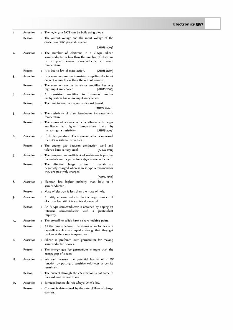
Electronics 1587
1. Assertion : The logic gate NOT can be built using diode.
Reason : The output voltage and the input voltage of the
diode have 180° phase difference.
[AIIMS 2005]
2. Assertion : The number of electrons in a P-type silicon
semiconductor is less than the number of electrons in a pure silicon semiconductor at room temperature.
Reason : It is due to law of mass action. [AIIMS 2005]
3. Assertion : In a common emitter transistor amplifier the input current is much less than the output current.
Reason : The common emitter transistor amplifier has very high input impedance. [AIIMS 2005]
4. Assertion : A transistor amplifier in common emitter configuration has a low input impedence.
Reason : The base to emitter region is forward biased.
[AIIMS 2004]
5. Assertion : The resistivity of a semiconductor increases with temperature.
Reason : The atoms of a semiconductor vibrate with larger amplitude at higher temperature there by increasing it's resistivity. [AIIMS 2003]
6. Assertion : If the temperature of a semiconductor is increased then it's resistance decreases.
Reason : The energy gap between conduction band and
valence band is very small [AIIMS 1997]
7. Assertion : The temperature coefficient of resistance is positive for metals and negative for P-type semiconductor.
Reason : The effective charge carriers in metals are negatively charged whereas in P-type semiconductor they are positively charged.
[AIIMS 1996]
8. Assertion : Electron has higher mobility than hole in a
semiconductor.
Reason : Mass of electron is less than the mass of hole.
9. Assertion : An N-type semiconductor has a large number of electrons but still it is electrically neutral.
Reason : An N-type semiconductor is obtained by doping an intrinsic semiconductor with a pentavalent impurity.
10. Assertion : The crystalline solids have a sharp melting point.
Reason : All the bonds between the atoms or molecules of a
crystalline solids are equally strong, that they get broken at the same temperature.
11. Assertion : Silicon is preferred over germanium for making
semiconductor devices.
Reason : The energy gap for germanium is more than the
energy gap of silicon.
12. Assertion : We can measure the potential barrier of a PN
junction by putting a sensitive voltmeter across its terminals.
Reason : The current through the PN junction is not same in forward and reversed bias.
13. Assertion : Semiconductors do not Obey's Ohm's law.
Reason : Current is determined by the rate of flow of charge carriers.

1588 Electronics
14. Assertion : Two P-N junction diodes placed back to back, will as a NPN transistor.
Reason : The P-region of two PN junction diodes back to back will form the base of NPN transistor.
15. Assertion : In transistor common emitter mode as an amplifier is preferred over common base mode.
Reason : In common emitter mode the input signal is connected in series with the voltage applied to the base emitter function.
16. Assertion : The dominant mechanism for motion of charge carriers in forward and reverse biased silicon P-N junction are drift in both forward and reverse bias.
Reason : In reverse biasing, no current flow through the junction.
17. Assertion : A transistor is a voltage-operating device.
Reason : Base current is greater than the collector current.
18. Assertion : NAND or NOR gates are called digital building blocks.
Reason : The repeated use of NAND (or NOR) gates can produce all the basic or complicated gates.
19. Assertion : At 0 K Germanium is a superconductor.
Reason : At 0 K Germanium offers zero resistance.
20. Assertion : Base in a transistor is made very thin as compared to collector and emitter regions.
Reason : Due to thin base power gain and voltage gain is obtained by a transistor.
21. Assertion : The current gain in common base circuit is always less than one.
Reason : At constant collector voltage the change in collector current is more than the change in emitter current.
22. Assertion : V-i characteristic of P-N junction diode is same as that of any other conductor.
Reason : P-N junction diode behave as conductor at room temperature.
23. Assertion : Zener diode works on a principle of breakdown voltage.
Reason : Current increases suddenly after breakdown voltage.
24. Assertion : NOT gate is also called inverter circuit.
Reason : NOT gate inverts the input order.
25. Assertion : In vacuum tubes (valves), vacuum is necessary for the movement of electrons between electrodes otherwise electrons collide with air particle and loses their energy.
Reason : In semiconductors devices, external heating or vacuum is not required.
26. Assertion : The following circuit represents 'OR' gate
Reason : For the above circuit BABAXY
27. Assertion : A P-N photodiode is made from a semiconductor
for which Eg
= 2.8 eV. This photo diode will not
detect the wavelength of 6000 nm.
Reason : A PN photodiode detect wavelength if gEhc
.
28. Assertion : 29 is the equivalent decimal number of binary
number 11101.
Reason : (11101)2
= (1 24 + 1 23 + 1 22 + 0 21 + 1 20 )10
= (16 + 8 + 4 + 0 + 1)10
= (29)10
29. Assertion : When PN-junction is forward biased then motion of
charge carriers at junction is due to diffusion. In
reverse biasing. The cause of motion of charge is
drifting.
Reason : In the following circuit emitter is reverse biased and
collector is forward biased.
30. Assertion : De-morgan's theorem BABA may be
explained by the following circuit
Reason : In the following circuit, for output inputs ABC are
101
31. Assertion : In the following circuit the potential drop across
the resistance is zero.
Reason : The given resistance has low value.
Solids and Crystals
1 d 2 d 3 d 4 a 5 a
6 a 7 a 8 b 9 a 10 c
11 d 12 c 13 b 14 a 15 a
16 a 17 d 18 b 19 c 20 c
21 b 22 a 23 b 24 a 25 d
26 d 27 d 28 d
Semiconductors
A
B
Y
X
E
C B
0 V
+ 1 V
– 2 V
Y
A
B
C
A
B
=
Y Y
– 5V
R = 0.1
– 2V

Electronics 1589
1 c 2 b 3 d 4 b 5 b
6 b 7 b 8 c 9 d 10 a
11 b 12 a 13 a 14 d 15 c
16 b 17 b 18 b 19 c 20 c
21 d 22 b 23 ac 24 d 25 b
26 c 27 d 28 c 29 c 30 b
31 d 32 a 33 b 34 a 35 c
36 d 37 c 38 b 39 d 40 a
41 d 42 c 43 b 44 c 45 d
46 b 47 a 48 b 49 a 50 d
51 d 52 b 53 b 54 a 55 c
56 d 57 b 58 d 59 a 60 a
61 b 62 a 63 c 64 a 65 b
66 a 67 c 68 c 69 c 70 c
71 b 72 b 73 a 74 b 75 c
76 b 77 c 78 a 79 d 80 a
81 a 82 a 83 b 84 d 85 c
86 d 87 a 88 c 89 b 90 c
91 a 92 b 93 d 94 d 95 d
96 d 97 d 98 a 99 b 100 a
101 b
Semiconductor Diode
1 b 2 a 3 b 4 b 5 c
6 b 7 a 8 b 9 a 10 a
11 b 12 b 13 b 14 c 15 d
16 c 17 c 18 bc 19 c 20 d
21 d 22 b 23 d 24 c 25 c
26 b 27 b 28 b 29 c 30 b
31 b 32 c 33 d 34 c 35 d
36 a 37 b 38 b 39 d 40 a
41 b 42 a 43 b 44 a 45 a
46 b 47 b 48 a 49 c 50 d
51 d 52 a 53 c 54 c 55 b
56 d 57 a 58 a 59 c 60 a
61 b 62 c 63 a 64 c 65 a
66 b 67 c 68 c 69 d 70 a
71 c 72 a 73 d 74 d 75 c
76 a 77 c 78 c 79 c
Junction Transistor
1 a 2 c 3 a 4 d 5 d
6 b 7 d 8 b 9 b 10 b
11 c 12 d 13 d 14 a 15 b
16 b 17 d 18 b 19 ac 20 a
21 c 22 a 23 b 24 b 25 b
26 c 27 a 28 b 29 b 30 d
31 b 32 b 33 a 34 b 35 b
36 a 37 a 38 a 39 b 40 a
41 b 42 d 43 d 44 b
Digital Electronics
1 b 2 c 3 b 4 a 5 b
6 c 7 d 8 b 9 a 10 a
11 d 12 b 13 c 14 a 15 c
16 a 17 b 18 b 19 a 20 a
21 b 22 c 23 b 24 c 25 b
26 c 27 b 28 a 29 a 30 d
31 d
Valve Electronics
1 c 2 c 3 a 4 b 5 b
6 b 7 c 8 b 9 a 10 a
11 c 12 b 13 b 14 c 15 d
16 b 17 b 18 c 19 c 20 c
21 b 22 b 23 b 24 c 25 a
26 c 27 d 28 a 29 a 30 ad
31 d 32 c 33 c 34 a 35 a
36 c 37 b 38 d 39 b 40 c
41 c 42 b 43 d 44 b 45 c
46 c 47 b 48 b 49 a 50 c
51 a 52 b 53 b 54 a 55 c
56 a 57 a 58 d
Critical Thinking Questions
1 c 2 a 3 c 4 c 5 abd
6 a 7 a 8 c 9 b 10 b
11 d 12 c 13 a 14 b 15 a
16 d 17 b 18 a 19 a 20 c
21 b 22 a 23 d 24 d 25 a
26 b 27 b 28 d 29 c 30 a
31 b 32 c 33 d 34 b 35 c
36 b 37 d 38 d 39 d 40 b
41 c 42 a 43 a 44 b 45 a
46 c 47 a 48 a 49 b 50 b
Graphical Questions
1 c 2 b 3 c 4 c 5 a

1590 Electronics
6 b 7 b 8 c 9 b 10 a
11 b 12 a 13 d 14 a 15 d
16 a 17 c 18 c 19 a 20 c
21 c 22 c 23 a 24 b 25 c
26 c 27 b 28 c 29 a 30 d
Assertion and Reason
1 d 2 a 3 c 4 a 5 d
6 a 7 b 8 a 9 b 10 a
11 c 12 e 13 e 14 d 15 b
16 d 17 d 18 a 19 d 20 a
21 c 22 d 23 a 24 a 25 b
26 a 27 a 28 a 29 b 30 c
31 b
Solids and Crystals
1. (d) Ionic bonds cone into being when atoms that have low ionization energies, and hence lose electrons rapidly, interact with other atoms that and to acquire excess electrons. The former atoms give up electrons to the latter and they there upon become positive and negative ions respectively.
2. (d) For tetragonal, cubic and orthorhombic system
.90
3. (d) Tourmaline crystal is biaxial.
4. (a) The temperature co-efficient of resistance of conductor is positive.
5. (a) Density 3)(aN
nA
where n = 2 for bcc structure , A = 39 10–3 kg,
N = 6.02 1023, a md )10525.4(3
2
3
2 10
(d = nearest neighbour distance = distance between centres of
two neighbouring atoms 2
a )
On putting the values we get = 907
6. (a) The highest energy level which an electron can occupy in the valence band at 0 K, is called Fermi energy level.
7. (a) In a triclinic crystal a b c and 90°
8. (b) Metallic solids are opaque because incident light is absorbed by the free electrons in a metal.
9. (a) In ionic bonding electrons are transferred from one type of atoms to the other type creating positive and negative ions. For example in NaCl, Na loses one electrons and Cl gains one so that Na+ and Cl– ions have a stable shell structure.
10. (c) Wood is non-crystalline.
11. (d) Cu has fcc structure, for fcc structure co-ordination number =
12
12. (c) Vander Waal force is weak dipole-dipole interaction.
13. (b)
14. (a) The sodium chloride crystal structure has a fcc lattice with one
chloride ion at each lattice point and one sodium ion half a
cube length above it.
15. (a) In NaCl crystal Na+ ion is surrounded by Cl6 ion, therefore
coordination number of Na+ is 6.
16. (a) Sodium has bcc structure. The distance between body centre
and a corner 2
3 a
Å66.32
225.43
17. (d)
18. (b) For the fcc structure
2/122 )(4 aar 2a
224
2 aar
19. (c) Metals reflects incident light by the vibrations of free electrons under the influence of electric field of incident wave. The conductivity of metals decreases with increase of temperature due to increase in random motion of free electrons. The bonding is therefore metallic.
20. (c)
21. (b) The nearest distance between two atoms in a bcc lattice = 2
(atomic radius) 2
3
4
32
aa
22. (a) The net force on electron placed at the centre of bcc structure is zero. (By the principle of superposition of couloumb forces)
23. (b) For bcc packing, distance between two nearest atoms
4
322
ard
Lattice constant Åd
a 3.43
7.32
3
2
24. (a)
25. (d) ra 42 Årr
a 59.354.22)2(22
4
26. (d)
27. (d) Covalent bonding exists in semi-conductor.
28. (d) In H2
O covalent bonding is present.
Semiconductors
1. (c) In P-type semiconductors, holes are the majority charge carriers
2. (b) Ga has a valancy of 3.
3. (d) Ge + impurity
Trivalent
torsemiconduc
type-P
4. (b) Since ne
> nh
; the semiconductor is N-type.
r
r
r
r
a
a
a
a
a

Electronics 1591
5. (b) Absence of one electron, creates the positive charge of magnitude equal to that of electronic charge.
6. (b) Ge + impurity
tPantavalen
torsemiconduc
type-N
7. (b) Impurity increases the conductivity.
8. (c) torsemiconduc
Intrinsic Conductivity is due to the
breaking of covalent bond
torsemiconduc
Extrisnsic Conductivity is due to the
breaking of covalent bond and excess of charge carriers due to impurity.
9. (d) Resistance of conductors (Cu) decreases with decrease in temperature while that of semi-conductors (Ge) increases with decrease in temperature.
10. (a) Aluminum is trivalent impurity.
11. (b) With temperature rise conductivity of semiconductors increases.
12. (a)
13. (a) Similar to Q. 11
14. (d) In insulators, the forbidden energy gap is largest and it is of the order of 6 eV.
15. (c) N-type semiconductors are neutral because neutral atoms are added during doping.
16. (b)
17. (b) In insulators, the forbidden energy gap is very large, in case of
semiconductor it is moderate and in conductors the energy gap is zero.
18. (b) Similar to Q. 15.
19. (c) Phosphorus is pentavalent.
20. (c) In intrinsic semiconductors, the creation or liberation of one free electron by the thermal energy has created one hole. Thus in intrinsic semiconductors n
e
= nh
21. (d) Conductor has positive temperature coefficient of resistance but semiconductor has negative temperature coefficient of resistance.
22. (b) Boron is trivalent.
23. (a, c) In intrinsic semiconductors, electrons and holes both are
charge carriers. In P-type semiconductors (Extrinsic semiconductors) holes are majority charge carriers.
24. (d)
25. (b)
26. (c) 67.0)( GermaniumgE eV
27. (d) In P-type semiconductors, holes are majority charge carrier and electrons are minority charge carriers.
28. (c) At zero Kelvin, there is no thermal agitation and therefore no
electrons from valence band are able to shift to conduction band.
29. (c) Antimony is a fifth group impurity and is therefore a donor of
electrons.
30. (b) Resistance of semiconductor eTemperatur
1
31. (d) S.C.
Extrinsic
)(Type
)(Type
pe
ep
nnN
nnP
32. (a) At room temperature the number of electrons and holes are equal in the intrinsic semiconductor.
33. (b) Indium is trivalent, hence on doping with it, the intrinsic semiconductor becomes P-type semiconductor.
34. (a)
35. (c) In semiconductors, Forbidden energy gap is of the order of 1 eV.
36. (d) At 0K temperature semiconductor behaves as an insulator, because at very low temperature electrons cannot jump from the valence band to conduction band.
37. (c) Antimony is pentavalent.
38. (b) At 0K semiconductor behaves as insulator so it's resistance is infinite.
39. (d) The conduction and valence bands in the conductors merge into each other.
40. (a) For N-type semiconductor, the impurity should be pentavalent.
41. (d) When a free electron is produced, simultaneously a hole is also produced.
42. (c) For P type semiconductor the doping impurity should be trivalent.
43. (b) The temperature co-efficient of resistance of a semiconductor is always negative.
44. (c) The resistance of semiconductor decreases with the increase in temperature.
45. (d) At absolute zero temperature, semiconductor.
46. (b) Formation of energy bands in solids are due to Pauli's exclusion principle.
47. (a) In P-type semiconductors, holes are majority charge carriers.
48. (b)
49. (a) Conductivity of semiconductors increases with rise in temperature.
50. (d) All are trivalent in nature.
51. (d) In N-type semiconductors, electrons are majority charge corners.
52. (b) When a strong current passes through the semiconductor it heats up the crystal and covalent bond are broken. Hence because of excess number of free electrons it behaves like a conductor.
53. (b)
54. (a) Phosphorus is a pentavalent impurity so ne
> nh
.
55. (c) Phosphorus is pentavalent while Indium is trivalent.
56. (d) Phosphorus and Arsenic both are pentavalent.
57. (b)
58. (d)
59. (a) For Ge, JJeVEg1919 1012.1106.17.07.0
60. (a) At room temperature some covalent bond breaks and semiconductor behaves slightly as a conductor.
61. (b)
62. (a)
V.B.
C.B.
Ef Energy gap (Eg)

1592 Electronics
63. (c) Because boron is a trivalent impurity.
64. (a) In P-type semi conductor, holes are majority charge carriers.
65. (b) In intrinsic semiconductors, at room temperature ne
= nh
.
66. (a) In conductors valence band and conduction band overlaps.
67. (c) Because As is pentavalent impurity.
68. (c) At 0 K semiconductor behaves as an insulator.
69. (c)
70. (c)
71. (b) Antimony and phosphorous both are pentavalent.
72. (b) Gallium is trivalent impurity.
73. (a)
74. (b) One atom of pentavalent impurity, donates one electron.
75. (c)
76. (b) The charge on hole is positive.
77. (c) Phosphorus is pentavalent impurity.
78. (a) ehi nnn 2 en 21219 10)10( ./10 317 mne
79. (d) Temperature co-efficient of semiconductor is negative.
80. (a) Copper, Aluminum, Iron are conductors, while Ge is semiconductor.
81. (a) At room temperature, few bonds breaks and electron hole pair generates inside the semiconductor.
82. (a)
83. (b) With rise in temperature, conductivity of semiconductor increases while resistance decreases.
84. (d) Gallium, boron and aluminum are trivalent.
85. (c) Because with rise in temperature, resistance of semiconductor decreases, hence overall resistance of the circuit increases, which in turn increases the current in the circuit.
86. (d) Extrinsic semiconductor (N-type or P-type) are neutral.
87. (a) Because eAn
iv
e
d)(
88. (c)
89. (b) Resistivity is the intrinsic property, it doesn't depend upon length and shape of the semiconductors.
90. (c)
91. (a) ÅE
hc10888
106.114.1
103106.619
834
max
92. (b) In N-type semiconductor impurity energy level lies just below the conduction band.
93. (d)
94. (d)
95. (d) eeen
316
390019/10
106.1
24.6cm
en
e
e
96. (d) In semiconductors, the forbidden energy gap between the valence band and conduction band is very small, almost equal to kT. Moreover, valence band is completely filled where as conduction band is empty.
97. (d) In sample x no impurity level seen, so it is undoped. In sample y impurity energy level lies below the conduction bond so it is doped with fifth group impurity.
In sample z, impurity energy level lies above the valence band so it is doped with third group impurity.
98. (a) Forbidden energy gap for carbon is greater than that of silicon.
99. (b)
100. (a) Because electrons needed less energy to move.
101. (b)

Electronics 1593
Semiconductor Diode
1. (b)
2. (a) In forward biased PN-junction, external voltage decreases the
potential barrier, so current is maximum. While in reversed
biased PN-junction, external voltage increases the potential
barrier, so the current is very small.
3. (b)
4. (b) Filter circuits are used to get smooth dc -filter is the best
filter.
5. (c) In reverse bias no current flows.
6. (b) In reverse biasing, width of depletion layer increases.
7. (a) Depletion layer consist of mainly stationary ions.
8. (b) Current flow is possible and AR
Vi 210
300
)14(
9. (a) The potential of P-side is more negative that of N-side, hence
diode is in reverse biasing. In reverse biasing it acts as open
circuit, hence no current flows.
10. (a)
11. (b) It is used to convert ac into dc (rectifier)
12. (b)
13. (b) Because in case (1) N is connected with N. This is not a series
combination of transistor.
14. (c)
15. (d)
16. (c) After a large reverse voltage is PN-junction diode, a huge
current flows in the reverse direction suddenly. This is called
Breakdown of PN-junction diode.
17. (c) In forward biasing both positive and negative charge carriers
move towards the junction.
18. (b,c)
19. (c) When polarity of the battery is reversed, the P-N junction
becomes reverse biased so no current flows.
20. (d) Resistance in forward biasing 10frR and resistance in
reverse biasing 510RwR 410
1
Rw
fr
R
R
21. (d)
22. (b) In forward biasing width of depletion layer decreases.
23. (d)
24. (c) At junction a potential barrier/depletion layer is formed, with
N-side at higher potential and P-side at lower potential.
Therefore there is an electric field at the junction directed from
the N-side to P-side
25. (c) In N-type semiconductor majority charge carriers are electrons.
26. (b) In forward biasing the diffusion current increases and drift current remains constant so not current is due to the diffusion.
In reverse biasing diffusion becomes more difficult so net current (very small) is due to the drift.
27. (b) At a particular reverse voltage in PN-junction, a huge current flows in reverse direction known as avalanche current.
28. (b) Due to the large concentration of electrons in N-side and holes in P-side, they diffuses from their own side to other side. Hence depletion region produces.
29. (c) Only in option (c), P-side is more negative as compared to N-side.
30. (b) Depletion layer is more in less doped side.
31. (b) In forward biasing P-side is connected with positive terminal and N-side with negative terminal of the battery
32. (c) In forward biasing of PN-junction diode, current mainly flows due to the diffusion of majority charge carriers.
33. (d)
34. (c) In forward biasing of PN junction diode width of depletion layer decreases. In intrinsic semiconductor fermi energy level is exactly in the middle of the forbidden gap
35. (d)
36. (a) At high reverse voltage, the minority charge carriers, acquires
very high velocities. These by collision break down the covalent
bonds, generating more carriers. This mechanism is called
Avalanche breakdown.
37. (b) Because P-side is more negative as compared to N-side.
38. (b) When reverse bias is increased, the electric field at the junction also increases. At some stage the electric field breaks the
covalent bond, thus the large number of charge carriers are generated. This is called Zener breakdown.
39. (d) In forward biasing both VB
and x decreases.
40. (a)
41. (b) In figure 2,4 and 5. P-crystals are more positive as compared to N-crystals.
42. (a) ac Rectifier dc
43. (b) In this condition NP junction is reverse biased.
44. (a)
45. (a) mVd
VE /10
105
5.0 6
7
.
C.B.
Ef
V.B.
E N P
Holes
Electrons
N P
+ –

1594 Electronics
46. (b) Across the NP junction, a barrier potential is developed
whose direction is from N region to P region.
47. (b)
48. (a) In forward biasing, resistance of PN junction diode is zero, so
whole voltage appears across the resistance.
49. (c)
50. (d) The electric field strength versus distance curve across the P-N junction is as follows
51. (d)
52. (a) It doesn't Obey's ohms law.
53. (c) Because N-side is more positive as compared to P-side.
54. (c) When a light (wavelength sufficient to break the covalent bond) falls on the junction, new hole electron pairs are created. No. of produced electron hole pair deponed upon no. of photons. So photo emf or current proportional to intensity of
light.
55. (b)
56. (d) For full wave rectifier
L
f
R
r
1
2.81
%2.81max n (rf
<< RL
)
57. (a)
58. (a)
59. (c) In reverse biasing negative terminal of the battery is connected
to N-side.
60. (a) In the given condition diode is in reverse biasing so it acts as open circuit. Hence potential difference between A and B is 6V
61. (b) Zener breakdown can occur in heavily doped diodes. In lightly doped diodes the necessary voltage is higher, and avalanche multiplication is then the chief process involved.
62. (c)
63. (a)
64. (c) Diode acts as open switch only when it is reverse biased
65. (a) Because P-side is more negative than N-side.
66. (b) In unbiased condition of PN-junction, depletion region is generated which stops the movement of charge carriers.
67. (c) For a wide range of values of load resistance, the current in the zener diode may change but the voltage across it remains unaffected. Thus the output voltage across the zener diode is a regulated voltage.
68. (c)
69. (d) Arsenic has five valence electrons, so it a donor impurity. Hence X becomes N-type semiconductor. Indium has only three outer electrons, so it is an acceptor impurity. Hence Y becomes P-type semiconductor. Also N (i.e. X) is connected to positive terminal of battery and P(i.e. Y) is connected to negative terminal of battery so PN-junction is reverse biased.
70. (a)
71. (c) In photodiode, it is illuminated by light radiations, which in turn produces electric current.
72. (a)
73. (d)
74. (d) By using mVd
VE /106
10
6.0 5
6
75. (c) The given circuit is full wave rectifier.
76. (a) The diode is in reverse biasing so current through it is zero.
77. (c) In full wave rectifier, the fundamental frequency in ripple is twice that of input frequency.
78. (c)
79. (c) IRVV '
= 0.5 + 0.1 20
= 2.5 V
Junction Transistor
1. (a) When NPN transistor is used as an amplifier, majority charge
carrier electrons of N-type emitter move from emitter to base and
than base to collector.
2. (c)
3. (a) In oscillator, a portion of the output power is returned back
(feed back) to the input in phase with the starting power. This
process is termed as positive feedback.
4. (d) The emitter base junction is forward biased while collector base
junction is reversed biased.
5. (d) Given ec ii 100
80ei
100
8024 mAie 30
By using cbe iii ib
= 30 – 24 = 6 mA.
6. (b)
7. (d) is the ratio of collector current and emitter current while is the ratio of collector current and base current.
8. (b)
9. (b) 98.01
98.0
1
=49.
10. (b) 96.01
96.0
1
=24.
P N
Distance
Electric field
0.1 A
20
Input signal Output amplified signal
Phase change
of
Transistor
amplifier
Feed back
network
Out put
N N
P Forward biased
reverse
biased

Electronics 1595
11. (c) e
c
i
i =0.96 and i
e
= 7.2 mA
ec ii 96.0 = 0.96 7.2 = 6.91 mA
bce iii 7.2 = 6.91 + ib
ib
= 0.29 mA.
12. (d)
13. (d) EC ii 100
90 10 = 0.9 i
E
= 11mA
Also CBE iii .11011 mAiB
14. (a) Current gain b
c
i
i
bc ii = 80 250 A.
15. (b) In transistor, base is least doped.
16. (b)
17. (d) = 50, Ri
= 1000 , Vi
= 0.01V
b
c
i
i and A
R
Vi
i
ib
5
310
10
01.0
Hence AAic 5001050 5 .
18. (b) 99.0991
99
1
.
19. (a,c) The circuit of a CE amplifier is as shown below.
This has been shown a NPN transistor. Therefore base emitter
are forward, biased and input signal is connected between base
and emitter.
20. (a) The base is always thin
21. (c) Voltage gain = Resistance gain
99)99.01(
99.0
1
Resistance gain 1010
10103
3
Voltage gain = 99 10 = 990.
22. (a) The arrow head in the transistor symbol always shows the
direction of hole flow in the emitter region.
23. (b)
24. (b) Because emitter (N) is common to both, base (P) and collector (N).
25. (b) Emitter is heavily doped.
26. (c) = 0.8 )8.01(
8.0
=4
Also b
c
i
i
bc ii = 4 6 = 24mA.
27. (a) mAii ec 96.1298.0
mAiii ceb 04.096.12 .
28. (b) beccbe iiiiii
29. (b) 61035
9
bbbb RRiV =257 k.
30. (d) bce iii
8 = 7.8 + bi bi =0.2mA = 200 A.
31. (b) b
c
i
i
32. (b) FET is unipolar.
33. (a)
34. (b) cbe iii 1c
b
c
e
i
i
i
i1
11
)1(
.
35. (b) In NPN transistor when emitter-base is forward biased, electrons move from emitter to base.
36. (a) Here VVc 5.0 , ci =0.05mA = 0.05 10–3A
Output resistance is given by
4
310
1005.0
5.0
c
cout
i
VR = 10k.
37. (a) Oscillator can produce radio waves of constant amplitude.
38. (a) 822.83.8
2.8
ceVb
cfe
i
ih
39. (b) Current gainb
c
i
i
Aib
53
10100
101
=0.01mA.
By using cbe iii ei = 1.01 + 1 = 1.01mA.
40. (a) In CB amplifier Input and output voltage signal are in same phase.
41. (b)
42. (d)
43. (d) For CE configuration voltage gain iL RR /
Power gain iL RR /2 gain Voltage
gainPower
44. (b) As we know BCE iii
c
b
c
e
i
i
i
i 1
11
1
1.
Digital Electronics
1. (b)
2. (c)
3. (b) For ‘OR’ gate BAX
N N
P
ie ib
ie
B
C
Output RL Ri
Input

1596 Electronics
i.e. 000 , 110 , 101 , 111
4. (a)
BABABAC . (De morgan’s theorem)
Hence output C is equivalent to OR gate.
ABABABABABABABC .
In this case output C is equivalent to AND gate.
5. (b) In ‘NOR’ gate BAY
i.e. 1000 , 0101
0110 , 0111
6. (c) For ‘XNOR’ gate ABBAY
i.e. 1010.01.10.00.0
0001.00.11.01.0
0000.11.00.10.1
1101.10.01.11.1
7. (d) The output D for the given combination
CBACBAD )().(
If 0 CBA then 111000)00( D
If 1 BA , 0C then 110010)11( D
8. (b)
9. (a) The Boolean expression for ‘NOR’ gate is BAY
i.e. if 0 BA (Low), 1000 Y (High)
10. (a)
11. (d) The Boolean expression for ‘AND’ gate is QPR .
1.1 = 1, 1.0 = 0, 0.1 = 0, 0.0 = 0
12. (b) Two ‘NAND’ gates are required as follows
ABABABY .
13. (c) For ‘NAND’ gate (option c), output 101.0
14. (a) AND + NOT NAND
15. (c) For ‘NOT’ gate AX
16. (a) The given Boolean expression can be written as
).().()).(.().).(( BBABAABABABABAY
BABABA .
A B Y
0 0 1
1 0 0
0 1 0
1 1 0
17. (b) For ‘AND’ gate, if output is 1 then both inputs must be 1.
18. (b)
19. (a)
20. (a) The given symbol is of ‘AND’ gate.
21. (b) It is the symbol of ‘NOR’ gate.
22. (c) The Boolean expression for the given combination is
output CBAY ).(
The truth table is
A B C Y =(A+B).C
0 0 0 0
1 0 0 0
0 1 0 0
0 0 1 0
1 1 0 0
0 1 1 1
1 0 1 1
1 1 1 1
Hence 1A , 0B , 1C
23. (b)
BABABAY .
This output equation is equivalent to OR gate.
24. (c) If inputs are A and B then output for NAND gate is ABY
If 1 BA , 011.1 Y
25. (b)
26. (c)
BAY
According to De morgan’s theorem
BABABAY ..
C
A
B
B
A
A
B
B
A
Y
A
B
C
BA
A
B
Y
BA
Y
A
B

Electronics 1597
This is the output equation of ‘AND’ gate.
27. (b) The output of OR gate is BAY .
28. (a) The given symbol is of NAND gate.
29. (a) 02020212)100010( 23452
0212 01 10)34(0200032
and 1212021212)11011( 012342
10)27(120816
Sum 10101022 )61()27()34()11011()100010(
Now
2 61 Remainder
2 30 1 LSD
2 15 0
2 7 1
2 3 1
2 1 1
0 1 MSD
Required sum (in binary system)
222 )111101()11011()100010(
30. (d) For ‘NAND’ gate BAC .
i.e. 100.0 , 101.0
100.1 , 011.1
31. (d) ‘NOR’ gates are considered as universal gates, because all the gates like AND, OR, NOT can be obtained by using only NOR gates.
Valve Electronics (Diode and Triode) 1. (c) According to Richardson-Dushman equation, number of
thermions emitted per sec per unit area kTW
eATJ/2 0
2TJ
2. (c) Intensity Number of electrons
3. (a) In SCR (Space charge region) electrons collect around the plate, this cloud decreases the emission of electrons from the cathode, hence plate current decreases.
4. (b)
5. (b) By using g
pm
v
ig
)3(1103 4
pi
mAAip 6.0106 4
6. (b) Voltage gain
L
pv
R
rA
1
and mp gr
21000102
423pr 57.29
1050
210001
42
3
vA
7. (c) Voltage gain
L
pv
R
rA
1
, for Lp Rr
2
vA
8. (b) When grid is given positive potential more electrons will cross
the grid to reach the positive plate P. Hence current increases.
9. (a) By using g
p
V
V
mp gr
gV 50
105.2107 33 VVg 86.2 .
10. (a) Using voltage gain
L
pv
R
rA
1
also mp gr
3103
20
m
pg
r
43 103103
201
20
vA =11
180=16.36.
11. (c) Voltage gain
L
p
R
rV
V
1in
out
3
3
out
1010
10401
25
5.0
V
VV 5.2out .
12. (b) G
p
V
V
)2.0(20 Gp VV = 4V.
13. (b) Voltage gain
L
pV
R
rA
1
and mp gr
301031010 33
.20303
2
3
2
21
p
pv
r
rA
14. (c)
15. (d) After saturation plate current can be increased by increasing the temperature of filament. It can be done by increasing the filament current.
16. (b) The maximum voltage gain (Av
)max
=
(Which is obtained when RL
= ).
17. (b) Voltage gain
L
pv
R
rA
1
pL rR 5.1
5
3
5.11
p
pv
r
rA 1220
5
3 .
18. (c)
19. (c)
20. (c) g
p
V
V
gp VV =15 0.3 = 4.5 volt.
K
G
P

1598 Electronics
21. (b) Plate resistance
6
3310
1010
1
slope
1
= 1000 k (static).
22. (b) Using
L
pv
R
rA
1
and mp gr
3
31025
102
50
m
pg
r
.25
1025
10251
50
3
3
vA
23. (b) Vi
PVViP 200
106.11014
104481915
3
24. (c) )(
(
21
21
GG
pp
VV
VV
.25
)3.15.0(
)220200(
25. (a) .300
1
6600
22
p
mmpr
ggr
26. (c) 310)42(
10075
21
21
Pp
pp
pII
VVr =12.5 103 =12.5k.
27. (d)
28. (a)
29. (a) Voltage amplification
L
pv
R
rA
1
310501
25
pr
......(i)
and
3101001
30
pr
......(ii)
an solving equation (i) and (ii), .25 krp
30. (a, d)
31. (d)
32. (c) Before saturation region, linear region comes. In linear region
pp Vi
1
2
200
400
2
1
2
1 p
p
V
V
i
i.
33. (c) ip
= 1.125 – 1.112 = 0.013A = 13 mA.
34. (a)
35. (a)
36. (c) Comparing the given equation with standard equation
kTqVeATi /2 V
kTVL .
37. (b)
38. (d)
k
i
Vr
p
p
p 1.11105.4
50
10)5.712(
100150 3
3.
39. (b)
40. (c) Voltage amplification pL
L
L
pv
rR
R
R
rA
1
4
3
44
42
2
1
A
A.
41. (c) A diode is used as a rectifier to convert ac in to dc.
42. (b) Fluctuating dc smooth dc.
43. (d)
44. (b)
45. (c) mp gr 310
20
pr = 2 104.
46. (c)
47. (b) g
p
V
V
gp VV =–50(–0.20) = 10V.
48. (b)
krp 5010102
1
slope
132
.
49. (a) Voltage amplification pL
Lmp
L
pv
rR
Rgr
R
rA
1
)1020(
105.2102010
3
33
L
L
R
R kRL 5 .
50. (c) Voltage gain 10
10
1081
18
14
3
L
pv
R
rA
.
51. (a) Ripple factor
1/
2/1
20
20
2
I
I
I
Ir
dc
rms =1.21.
52. (b)
53. (b)
54. (a) 34 102105.2 mp gr =50.
55. (c) 3.33)575.5(
)200225(
constant
pig
p
V
V
56. (a) mhomV
Ig
pVg
pm 2
)2.2(2.1
)5.55.7(
constant
57. (a)
58. (d) Using mp gr 3
3102
1010
20
mg .
Critical Thinking Questions
1. (c) Number density of atoms in silicon specimen = 5 1028 atom/m3
= 5 1022 atom/cm3
Since one atom of indium is doped in 5 107 Si atom. So
number of indium atoms doped per cm3 of silicon.
./101105
105 315
7
22
cmatomn
2. (a) The probability of electrons to be found in the conduction
band of an intrinsic semiconductor
Filter circuit

Electronics 1599
kT
EE F
e
EP)(
1
1)(
; where k = Boltzmann's constant
Hence, at a finite temperature, the probability decreases exponentially with increasing band gap.
3. (c) When donor impurity (+5 valence) added to a pure silicon (+4
valence), the +5 valence donor atom sits in the place of + 4 valence silicon atom. So it has a net additional + 1 electronic charge. The four valence electron form covalent bond and get fixed in the lattice. The fifth electron (with net – 1 electronic charge) can be approximated to revolve around + 1 additional charge. The situation is like the hydrogen atom for which
energy is given by eVn
E2
6.13 . For the case of hydrogen,
the permittivity was taken as 0
. However, if the medium has a
permittivity r
, relative to 0
, then eVn
Er
22
6.13
For Si, r
= 12 and for n = 1, eVE 1.0–~
4. (c) The forward current
110)1( 300104.1
2.0106.1
5/ 23
19
eeii kTeVs
A35 10376.20]16.2038[10
5. (a,b,d) At 0 K, a semiconductor becomes a perfect insulator. Therefore at 0 K, if some potential difference is applied across an insulator or a semiconductor, current is zero. But a conductor will become a superconductor at 0 K. Therefore, current will be infinite. In reverse biasing at 300 K through a
P-N junction diode, a small finite current flows due to minority charge carriers.
6. (a) Since diode in upper branch is forward biased and in lower branch is reversed biased. So current through circuit
drR
Vi
; here dr = diode resistance in forward biasing = 0
AR
Vi 2.0
10
2 .
7. (a) The voltage drop across resistance = 8 – 0.5 = 7.5 V
Current mAi 4.3102.2
5.73
8. (c)
hcE
E
hc
193
834
106.11057
103106.6
=217100Å.
9. (b) The diode in lower branch is forward biased and diode in upper branch is reverse biased
Ai50
5
3020
5
.
10. (b) The current through circuit AV
Pi 2.0
5.0
10100 3
voltage drop across resistance = 1.5 – 0.5 = 1 V
52.0
1R .
11. (d) In common emitter configuration current gain
36 1010251
50
1
Loe
fe
iRh
hA = – 48.78.
12. (c) Voltage gain voltageInput
voltageOutput
Vout
= Vin
Voltage gain
Vout
= Vin
Current gain Resistance gain
= Vin
BE
L
R
R= .1
1
1010010 3 V
13. (a) 318318 /105,/108 mnmn he
sec
01.0,sec
3.222
volt
m
volt
mhe
he nn so semiconductor is N-type
Also conductivity )()(yResistivit
1hhee nne
]01.01053.2108[106.11 181819
= 0.34 -m.
14. (b) VV
Vrms 1002
200
2
0
15. (a) At knee point voltage across the diode is 0.7V.
Hence voltage across resistance R is 5 – 0.7 = 4.3 V.
using V = iR 4.3 = 1 10–3 R R = 4.3 k.
16. (d) In positive half cycle one diode is in forward biasing and other
is in reverse biasing while in negative half cycle their polarity
reverses, and direction of current is opposite through R for
positive and negative half cycles so out put is not rectified.
Since R1
and R2
are different hence the peaks during positive
half and negative half of the input signal will be different.
17. (b) In half wave rectifier
100 V
Vdc
18. (a) In common base mode = 0.98, R = 5 k, Rin
= 70
voltage gain 7070
10598.0
3
in
vR
RA
Power gain = Current gain Voltage gain
= 0.98 70 = 68.6
19. (a) 53.015
)5(12
22
orn a
Z
nr = 10.6 Å.
20. (c) (i) VA
= –10V and VB
= –5V
Diodes D1
and D3
are reveres biased and D2
is forward biased.
R
R
R
A B
4
R 4
R
– 10 V – 5 V

1600 Electronics
RRR
RRAB2
3
44 .
(ii) When VA
= – 5V and VB
= – 10V
Diodes D2
is reverse biased D1
and D3
are forward biased
424
RRRRAB =R.
(iii) In this case equivalent resistance between A and B is also
R.
Hence (ii) = (iii) < (i).
21. (b) According to the given polarity, diode D1
is forward biased
while D2
is reverse biased. Hence current will pass through D1
only.
So current Ai 02.0)10050150(
6
22. (a) Diode is in forwards biasing hence the circuit can be redrawn
as follows
VVAB 105)510(
30
23. (d) The diode D will conduct for positive half cycle of a.c. supply
because this is forward biased. For negative half cycle of a.c.
supply, this is reverse biased and does not conduct. So out put
would be half wave rectified and for half wave rectified out put
2
200
2
2200
2
0 V
Vrms
24. (d) )14.036.0(106.1102)( 1919 hene
1)-(6.1 m
8
25
106.1
105.04
3
A
l
A
lR
AAR
Vi 64.0
25
16
8/25
2
25. (a) As we know current density J = nqv
eee qvnJ and hhh qvnJ
h
e
h
e
h
e
v
v
n
n
J
J
20
5
4/1
4/3
h
e
n
n
5
6
h
e
n
n
26. (b) Consider the case when Ge and Si diodes are connected as
show in the given figure.
Equivalent voltage drop across the combination Ge and Si
diode = 0.3 V
Current mAk
i 34.25
3.012
Out put voltage V0
= Ri
= 5 k 2.34 mA = 11.7 V
Now consider the case when diode connection are reversed. In
this case voltage drop across the diode's combination = 0.7 V
Current mAk
i 26.25
7.012
VkmAiRV 3.11526.20
Hence charge in the value of V0
= 11.7 –11.3 = 0.4 V
27. (b) For the positive half cycle of input the resulting network is
shown below
(V0
)max
= .5102
1)(
2
1max VVi
28. (d) The equivalent circuit can be redrawn as follows
From figure it is clear that current drawn from the battery
mAii 52
102 and .01 i
29. (c) mAib 5.06.8
7.05
mAII bc 5.0100
By using VRIVV LcCCCE 13100105018 3
30. (a) mAIe 6.110
1106.110
6
1910
t
QI
Since 2% electrons are absorbed by base, hence 98% electrons
reaches the collector i.e. = 0.98
mAmAII ec 57.1568.16.198.0
Also current amplification factor 4902.0
98.0
1
31. (b)
R
R
R
A B
4
R 4
R
– 5 V – 10 V
Vi
10 V
0 T/2 t
D1 D2
2k 2k
2k
+ – V0
+
–
2k
+
–
2k
2k
A B
(A + B)
G1
G2
G3
Y
BA
A
B
30V 10
10 10 VAB
Parallel
52
10
12k
10 V
i1
14k
2k
i2
i
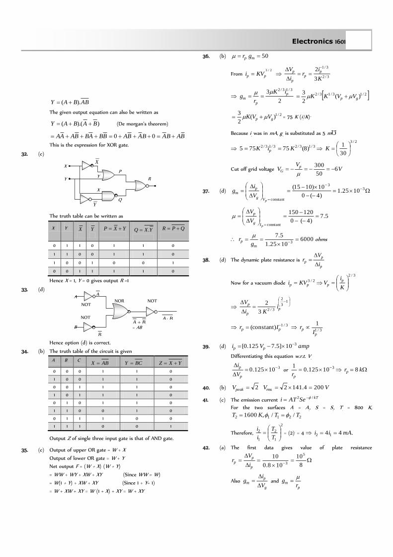
Electronics 1601
ABBAY ).(
The given output equation can also be written as
)).(( BABAY (De morgan’s theorem)
BABABABABBABBAAA 00
This is the expression for XOR gate.
32. (c)
The truth table can be written as
X Y X
Y
YXP
YXQ .
QPR
0 1 1 0 1 1 0
1 1 0 0 1 1 0
1 0 0 1 0 0 1
0 0 1 1 1 1 0
Hence X = 1, Y = 0 gives output R =1
33. (d)
Hence option (d) is correct.
34. (b) The truth table of the circuit is given
A B C ABX BCY YXZ
0 0 0 1 1 0
1 0 0 1 1 0
0 0 1 1 1 0
1 0 1 1 1 0
0 1 0 1 1 0
1 1 0 0 1 0
0 1 1 1 0 0
1 1 1 0 0 1
Output Z of single three input gate is that of AND gate.
35. (c) Output of upper OR gate = W + X
Output of lower OR gate = W + Y
Net output F = (W + X) (W + Y)
= WW + WY + XW + XY (Since WW = W)
= W(1 + Y) + XW + XY (Since 1 + Y= 1)
= W + XW + XY = W (1 + X) + XY = W + XY
36. (b) 50 mp gr
From 2/3
pp KVi 3/2
3/1
3
2
K
ir
i
V pp
p
p
2
3 3/13/2p
p
m
iK
rg
2/13/13/2 )(
2
3gp VVKK
2/1)(2
3gp VVK = 75 K (i
p
/K)1/3
Because ip
was in mA, gm
is substituted as 5 m℧
3/13/2755 piK 3/13/2 )8(75 K
2/3
30
1
K
Cut off grid voltage VV
Vp
G 650
300
37. (d)
33
constant
1025.1)4(0
10)1015(
pVg
pm
V
ig
5.7)4(0
120150
constant
pIg
p
V
V
60001025.1
5.73
m
pg
r
ohms
38. (d) The dynamic plate resistance is p
pp
i
Vr
Now for a vacuum diode
3/2
2/3
K
iVKVi
pppp
13
2
3/23
2p
p
pi
Ki
V
3/1constant)( pp Ir 3/1
1
p
pI
r
39. (d) ampVi pp310]5.7125.0[
Differentiating this equation w.r.t. Vp
310125.0
p
p
V
i or 310125.0
1 pr
krp 8
40. (b) VVV rmspeak 2004.14122
41. (c) The emission current kTSeATi /2
For the two surfaces A1
= A2
, S1
= S2
, T1
= 800 K,
22112 //,1600 TTKT
Therefore,
2
1
2
1
2
T
T
i
i= (2)2 = 4 .44 12 mAii
42. (a) The first data gives value of plate resistance
8
10
108.0
10 5
3p
p
pi
Vr
Also g
pm
V
ig
and
p
mr
g
Y
X X
R
Y
X
Y
Q
P
A
B
BA
NOR
BA
B
A
= AB
NOT
NOT
NOT

1602 Electronics
Vri
Vpp
g 25.68
8/10104 53
43. (a) 2/3)10(004.0 gpp VVI
10)10(
2
3004.0 2/1
gp
g
pVV
V
I
10)210120(2
3004.0 2/1 mg
mhommhogm 6.0106 4
Comparing the given equation of Ip
with standard equation 2/3)( gpp VVKI we get = 10
Also from = rp
gm
3106.0
10
m
pg
r
.67.161067.16 3 krp
44. (b) 505.220 mP gr
From LP
L
Rr
RA
L
LLLP R
R
A
RRr 5
10
50
kr
RrRp
LpL 54
20
44
45. (a) 11
84
1210
1214
Lp
L
Rr
RA
. Peak value of output signal
VV 2211
840 V
VVrms
11
284
2
0
r.m.s. value of current through the load
mAA 27.1101211
2843
46. (c)
4
6104
101600
64
m
pg
r
Voltage gain 32
1040
1041
64
13
4
L
pv
R
rA
Output signal voltage
.)..(321320 smrVVAV iv
Signal power in load mWR
V
L
6.251040
)32(3
220
47. (a) mAVVki gpp2/3)(
4 = k(200 – 10 4)3/2 = k (160)3/2 ….(i)
and 2/32/3 )90()710160( kkip ….(ii)
From equation (i) and (ii) we get
mAip 69.14
34
160
904
32/3
48. (a) At VVVV pg 300,3 and mAIp 5
At ,1VVg for constant plate current i.e. mAIp 5
From 5.7125.0 pp VI
5.7125.05 pV VVp 100
change in plate voltage VVp 200100300
Change in grid voltage VVg 2)3(1
So, 1002
200
g
p
V
V
49. (b) The slope of anode characteristic curve pr
1
A
V
mA
V
VmArp
3105050/02.0
1
The slope of mutual characteristic curve = gm
= 1 10–3 A/V.
50101050 33 mp gr .
50. (b) Voltage gain i
f
i
o
R
R
V
VA 100
1
100
k
k.
Graphical Questions 1. (c) With rise in temperature, resistivity of semiconductors
decreases exponentially.
2. (b) Potential across the PN junction varies symmetrically linear, having P side negative and N side positive.
3. (c) PN junction has low resistance in one direction of potential difference +V, so a large current flows (forward biasing). It has a high resistance in the opposite potential difference direction –V, so a very small current flows (Reverse biasing).
4. (c) When input voltage is – 10 V, the diode is reverse biased and no output is obtained. On the other hand, when input is +10V, the diode is forward biased and output is obtained which is +10V. Therefore the output is of the form as show in the following figure.
5. (a) In the depletion layer of PN junction, stationary, positive ions exists in the N-side and stationary negative ions exists in the P side.
6. (b) kV = knee voltage = 0.3 V
Resistance
k
i
V2.0200
10)010(
)3.03.2(3
– +
Rf
Vi Vo
Ri
–
+
Barrier potential
difference
PN junction
+ 10 V
0

Electronics 1603
7. (b) Half wave rectifier, rectifies only the half cycle of input ac signal and it blocks the other half.
8. (c) As RC time constant of the capacitor is quite large
( secRC 1.010101010 63 ), if will not
discharge appreciably. Hence voltage remains nearly constant.
9. (b) In the positive half cycle of input ac signal diode D1
is forward biased and D
2
is reverse biased so in the output voltage signal, A and C are due to D
1
. In negative half cycle of Input ac signal D
2
conducts, hence output signals B and D are due to D2
.
10. (a) If i is the current in the diode and V is voltage drop across it, then for given figure voltage equation is
8100 Vi 100
8
100
1 Vi 08.0)01.0( Vi
Thus the slope of i-V graph 01.01
LR
11. (b) The current at 2V is 400 mA and at 2.1 V it is 800 mA. The dynamic resistance in this region
25.0
4
1
10)400800(
)21.2(3i
VR
12. (a) From the given waveforms, the following truth table can be made
Time interval Inputs Output
A B Y
0 T1
0 0 0
T1
T2
0 1 0
T2
T3
1 0 0
T3
T4
1 1 1
This truth table is equivalent to ‘AND’ gate.
13. (d) 5 volt is low signal (0) and 10 volt is high signal (1) and taking
5 -sec as 1 unit. In a negative logic, low signal (0) gives high
output (1) and high signal (1) gives low output (0). The output is therefore 1010010111.
14. (a) mhomilliV
ig
g
pm 5.2
)24(
10)1520( 3
15. (d) The cut off grid voltage is that negative grid bias corresponding to which the plate current becomes zero. At point P, i
p
= 0
16. (a) According to Richardson-Dushman equation TbeATJ /2
Taking log of this equation T
bA
T
Jee loglog
2
i.e. graph between 2
logT
Je and
T
1 will be a straight line
having negative slope and positive intercept (loge
A) on
axis.log2T
Je
17. (c) TbeATJ /2 TbeT
J /
2
i.e. 2T
J will vary exponentially with
T
1, having negative slope.
18. (c) This is the graph between ip
and Vg
and ip
becomes zero at certain negative potential.
19. (a) 102
20
)]4(6[
)6080(
const.
pig
p
V
V
20. (c) According to
L
pv
R
rA
1
||
as RL
increases Av
also increases. When RL
becomes too high
then Av
= maximum =
Hence only option (c) is correct.
21. (c) With rise in temperature, work function decreases (non-linearly).
22. (c)
3.33310150
503
p
p
pi
VR
23. (a) 2Ti
2
00
T
T
i
i
This is the equation of a parabola.
24. (b) The band width is defined as the frequency band in which the
amplifier gain remains above 707.02
1 of the mid
frequency gain (Amax
). The low frequency f1
at which the gain falls
to 2
1 i.e. 0-.707 times it's mid frequency value is called
lower cut off frequency and the high frequency f4
at which the
gain falls to 2
1 i.e. 0.707 times of it's mid frequency is
known as higher cut off frequency so band width = f4
– f1
.
25. (c) rp
varies with ip
according to relation 3/1 pp ir i.e. when ip
increases, rp
decreases, hence graph C represents the variation of r
p
.
doesn't depends upon ip
, hence graph A is correct.
26. (c) From the graph it is clear that of for ,0,4 pg iVV so
cut off voltage is – 4 volt.
27. (b) As temperature increases saturation current also increases.
28. (c)
29. (a) Output signal voltage has phase difference of 180° with respect to input.
30. (d) Grid is maintained between 0 volt to certain negative voltage.
Assertion and Reason
1. (d) In diode the output is in same phase with the input therefore it
cannot be used to built NOT gate.
2. (a) According to law of mass action, hei nnn 2 . In intrinsic
semiconductors ni
= ne
= nh
and for P-type semiconductor ne
would be less than n
i
, since nh
is necessarily more than ni
.
3. (c) In common emitter transistor amplifier current gain ,1 so
output current > Input current, hence assertion is correct.
Also, input circuit has low resistance due to forward biasing to emitter base junction, hence reason is false.
4. (a) Input impedance of common emitter configuration
constant
CEVB
BE
i
V

1604 Electronics
where BEV voltage across base and emitter (base emitter
region is forward biased)
Bi base current which is order of few microampere.
Thus input impedance of common emitter is low.
5. (d) Resistivity of semiconductors decreases with temperature. The atoms of a semiconductor vibrate with larger amplitudes at higher temperatures there by increasing it's conductivity not resistivity.
6. (a) In semiconductors the energy gap between conduction band
and valence band is small ( 1 eV). Due to temperature rise, electron in the valence band gained thermal energy and may jump across the small energy gap, goes in to the conduction band. Thus conductivity increases and hence resistance decreases.
7. (b)
8. (a) The ratio of the velocity to the applied field is called the mobility. Since electron is lighter than holes, they move faster in applied field than holes.
9. (b)
10. (a) At a particular temperature all the bonds of crystalline solids breaks and show sharp melting point.
11. (c) The energy gap for germanium is less )72.0( eV than the
energy gap of silicon )1.1( eV . Therefore, silicon is preferred
over germanium for making semiconductor devices.
12. (e) We cannot measure the potential barrier of a PN-junction by connecting a sensitive voltmeter across its terminals because in the depletion region, there are no free electrons and holes and in the absence of forward biasing, PN- junction offers infinite resistance.
13. (e) The assertion is not true. In fact, semiconductor Obeys Ohm's law for low values of electric field (~ 106 V/m). Above this, the current becomes almost independent of electric field.
14. (d) Two PN-junctions placed back to back cannot work as NPN transistor because in transistor the width and concentration of doping of P-semiconductor is less as compared to width doping of N-type semiconductor type.
15. (b) Common emitter is prepared over common base because all the current, voltage and power gain of common emitter amplifier is much more than the gains of common base amplifier.
16. (d) In PN-junction, the diffusion of majority carriers takes place when junction is forward biased and drifting of minority carriers takes place across the function, when reverse biased. The reverse bias opposes the majority carriers but makes the minority carriers to cross the PN-junction. Thus the small
current in A flows during reverse bias.
17. (d) A transistor is a current operating device because the action of transistor is controlled by the charge carriers (electrons or holes). Base current is very much lesser than the collector current.
18. (a) These gates are called digital building blocks because using these gates only (either NAND or NOR) we can compile all other gates also (like OR, AND, NOT, XOR).
19. (d) At 0K, Germanium offers infinite resistance, and it behaves as an insulator.
20. (a) In a transistor, the base is made extremely thin to reduce the combinations of holes and electrons. Under this condition, most of the holes (or electrons) arriving from the emitter diffuses across the base and reach the collector. Hence, the collector current, is almost equal to the emitter current, the base current being comparatively much smaller. This is the main reason that
power gain and voltage gain are obtained by a transistor. If the base region was made quite thick, then majority of carriers from emitter will combine with the carriers in the base and only small number of carriers will reach the collector, so there would be little collector current and the purpose of transistor would be defeated.
21. (c) The current gain in common base circuit
CVE
C
I
I
The change in collector current is always less than the change in emitter current.
EC II . Therefore, .1
22. (d) The V-i characteristic of PN- diode depends whether the junction is forward biased or reverse biased. This can be showed by graph between voltage and current.
23. (a) When the reverse voltage across the zener diode is equal to or more than the breakdown voltage, the reverse current increases sharply.
24. (a)
If A = 0, Y = 1 and A = 1, Y = 0.
25. (b) In vacuum tubes, vacuum is necessary and the working of semiconductor devices is independent of heating or vacuum.
26. (a)
This is the Boolean expression for 'OR' gate.
27. (a) For detection of a particular wavelength () by a PN photo
diode, energy of incident light > Eg
gE
hc
For nmE
hceVE
g
g 9.441106.18.2
103106.6,8.2
19
834
i.e. ,6000 nmE
hc
g
so diode will not detect the wavelength
of 6000Å.
28. (a)
29. (b) In forward biasing of PN junction current flows due to diffusion of majority charge carriers. While in reverse biasing current flows due to drifting of minority charge carriers.
The circuit given in the reason is a PNP transistor having emitter is more negative w.r.t. base so it is reverse biased and collector is more positive w.r.t. base so it is forward biased.
30. (c) Assertion is true but reason is false
+ Intrinsic
semiconductor
(Neutral)
Pentalvalent
impurity
(Neutral)
N-type semiconductor
(Neutral)
Reverse
bias (V)
Knee voltage forward bias
(V)
Reverse cu
rrent
(A)
Zener
voltage
Forw
ard
curr
ent
(A)
Input (A) Output (Y)
A
B
BABAXY BAX
CABY ).(
A
B
C
AB

Electronics 1605
If A = 1, B = 0, C = 1 then Y = 0
31. (b) Both assertion and reason are true but potential difference across the resistance is zero, because diode is in reverse biasing hence no current flows.

1606 Electronics
1. In a pure silicon (ni
= 1016/m3) crystal at 300 K, 1021 atoms of phosphorus are added per cubic meter. The new hole concentration will be
(a) 1021 per m3 (b) 1019 per m3
(c) 1011 per m3 (d) 105 per m3
2. In the Boolean algebra ABA )( equals to
(a) BA (b) A
(c) BA (d) A + B
3. In a given circuit as shown the two input waveform A and B are applied simultaneously. The resultant waveform Y is
(a) (b)
(c) (d)
4. Two identical capacitors A and B are charged to the same potential V and are connected in two circuits at t = 0, as shown in figure. The charge on the capacitors at time t = CR are respectively
(a) VC, VC (b) VCe
VC,
(c) VC, e
VC (d)
e
VC
e
VC,
5. In transistor, forward bias is always smaller than the reverse bias. The correct reason is
(a) To avoid excessive heating of transistor
(b) To maintain a constant base current
(c) To produce large voltage gain
(d) None of these
6. In NPN transistor, if doping in base region is increased then collector current
(a) Increases (b) Decreases
(c) Remain same (d) None of these
7. In the following circuit I1
and I2
are respectively
(a) 0, 0
(b) 5 mA, 5 mA
(c) 5 mA, 0
(d) 0, 5 mA
8. In space charge limited region, the plate current in a diode is 10 mA
for plate voltage 150 V. If the plate voltage is increased to 600 V,
then the plate current will be
(a) 10 mA (b) 40 mA
(c) 80 mA (d) 160 mA
9. A triode has a plate resistance of 10 k and amplification factor 24.
If the input signal voltage is 0.4 V (r.m.s.), and the load resistance is
10 k ohm, then, the output voltage (r.m.s.) is
(a) 4.8 V (b) 9.6 V
(c) 12.0 V (d) None of these
10. Pure sodium (Na) is a good conductor of electricity because the 3s
and 3p atomic bands overlap to form a partially filled conduction
band. By contrast the ionic sodium chloride (NaCl) crystal is
(a) Insulator (b) Conductor
(c) Semiconductor (d) None of these
11. Would there be any advantage to adding n-type or p-type impurities
to copper
(a) Yes (b) No
(c) May be (d) Information is insufficient
12. In the following common emitter circuit if = 100, VCE
= 7V, VBE
=
Negligible RC
= 2 k then IB
= ?
(a) 0.01 mA
(b) 0.04 mA
(c) 0.02 mA
(d) 0.03 mA
13. When a battery is connected to a P-type semiconductor with a
metallic wire, the current in the semiconductor (predominantly),
inside the metallic wire and that inside the battery respectively due
to
(a) Holes, electrons, ions (b) Holes, ions, electrons
(c) Electrons, ions, holes (d) Ions, electrons, holes
14. Is the ionisation energy of an isolated free atom different from the
ionisation energy Eg
for the atoms in a crystalline lattice
(a) Yes (b) No
(c) May be (d) None of these
12k
10 V
i1
14k
2k
i2
A
B
Y
C
R
+ –
(i)
C
+ –
(ii)
R 15 V
RB
iB iC
B
C
E
RC

Electronics 1607
15. In the following circuit, a voltmeter V is connected across a lamp L.
What change would occur in voltmeter reading if the resistance R is
reduced in value
(a) Increases (b) Decreases
(c) Remains same (d) None of these
16. For given electric voltage signal dc value is
(a) 6.28 V (b) 3.14 V
(c) 4 V (d) 0 V
17. When a silicon PN junction is in forward biased condition with
series resistance, it has knee voltage of 0.6 V. Current flow in it is 5
mA, when PN junction is connected with 2.6V battery, the value of
series resistance is
(a) 100 (b) 200
(c) 400 (d) 500
18. In the following circuit the equivalent resistance between A and B is
(a) 3
20 (b) 10
(c) 16 (d) 20
19. In the following circuit of PN junction diodes D1
, D2
and D3
are ideal
then i is
(a) E/R (b) E/2R
(c) 2E/3R (d) Zero
20. In circuit in following fig. the value of Y is
(a) 0
(b) 1
(c) Fluctuates between 0 and 1
(d) Indeterminate as the circuit can’t be realised
21. A waveform shown when applied to the following circuit will
produce which of the following output waveform. Assuming ideal
diode configuration and 21 RR
(a) (b)
(c) (d)
22. In a triode, cathode, grid and plate are at 0, – 2 and 80 V
respectively. The electrons is emitted from the cathode with energy
3 eV. The energy of the electron reaching the plate is
(a) 77 eV (b) 85 eV
(c) 81 eV (d) 83 eV
23. The energy gap of silicon is 1.5 eV. At what wavelength the silicon
will stop to absorb the photon
(a) 8250 Å (b) 7250 Å
(c) 6875.5 Å (d) 5000 Å
1. (c) By using mass action law hei nnn 2
311
21
2162
1010
)10(mper
n
nn
e
ih
2. (b) ABAABAABA )()()(
= AA + AB = A + AB = A(1 + B) = A
3. (a) (1 = high, 0 = low)
(SET -27)
L V
R
VBB
+ –
VCC
6.28V
t
V
A
– 10V 8 12
2
6 4
B
– 2V
i D3
D2
D1
R
R
R
E
1
G1 0
G2
G3
B
A y
R1
V0 R2
– 5 V
5 V
Vin
+ 5V
– 5V
2.5V
– 2.5V
1608 Electronics
Input to A is in the sequence, 1,0,1,0.
Input to B is in the sequence, 1, 0, 0, 1.
Sequence is inverted by NOT gate.
Thus inputs to OR gate becomes 0, 1, 0, 1 and output of OR gate becomes 0, 1, 1, 1
Since for OR gate 0 + 1 = 1. Hence choice (a) is correct.
4. (b) Time t = CR is known as time constant. It is time in which
charge on the capacitor decreases to e
1 times of it’s initial
charge (steady state charge).
In figure (i) PN junction diode is in forward bias, so current will flow the circuit i.e., charge on the capacitor decrease and in
time t it becomes )(1
oQe
Q ; where CVQo
e
CVQ
In figure (ii) P-N junction diode is in reverse bias, so no current will flow through the circuit hence change on capacitor will not decay and it remains same i.e. CV after time t.
5. (a) If forward bias is made large, the majority charge carriers would move from the emitter to the collector through the base with high velocity. This would give rise to excessive heat causing damage to transistor.
6. (b) Number of holes in base region increases hence recombination of electron and hole are also increases in this region. As result base current increases which in turn decreases the collector current.
7. (d) Equivalent circuit can be redrawn as follows
252
10imAi
i1
= 0
8. (c) In space charge limited region, the plate current is given by
Child's law 2/3pp KVi
Thus, 8)4(150
600 2/3
2/32/3
1
2
1
2
p
p
p
p
V
V
i
i
or 812 pp ii = 10 8 mA = 80 mA.
9. (a) Use sAVV 0
Now 1220
1024
1010
1024
kk
kA
Therefore, .)..(8.44.0120 smrvoltV
10. (a) In sodium chloride the Na and Cl ions both have noble
gas electron configuration corresponding to completely filled bands. Since the bands do not overlap, there must be a gap
between the filled bands and the empty bands above them, so NaCl is an insulator.
11. (b) Pure Cu is already an excellent conductor, since it has a partially filled conduction band, furthermore, Cu forms a
metallic crystal as opposed to the covalent crystals of silicon or germanium, so the scheme of using an impurity to donate or accept an electron does not work for copper. In fact adding
impurities to copper decreases the conductivity because an impurity tends to scatter electrons, impeding the flow of current.
12. (b) LCCE RIVV
15 = 7 + IC
2 103 iC
= 4 mA
B
C
i
i mAiB 04.0
100
4
13. (a) Charge carriers inside the P-type semiconductor are holes (mainly). Inside the conductor charge carriers are electrons and for cell ions are the charge carriers.
14. (a) The ionisation energy of an isolated atom is different from it’s value in crystalline lattice, because in the latter case each bound electron is influenced by many atoms in the periodic crystalline lattice.
15. (a) Here the emitter base junction of N-P-N transistor is forward biased with battery V
BB
through resistance R. When the value of R is reduced, then the emitter current i
e
will increase. As a result the collector current will also increase. (i
c
= ie
– ib
). Due to increase in i
c
, the potential difference across L increases and
hence the reading of voltmeter will increases.
16. (c) .414.3
28.622 0 VV
VV acdc
17. (c)
3105
)6.06.2(
R = 400 .
18. (c) According to the given figure A is at lower potential w.r.t. B.
Hence both diodes are in reverse biasing, so equivalent, circuit
can be redrawn as follows.
Equivalent resistance between A and B
R = 8 + 2 + 6 = 16 .
19. (a) Diodes D1
and D3
are forward biased and D2
is reverse biased so
the circuit can be redrawn as follows.
R
Ei
20. (a) Lower NOT gate inverts input to zero. NOT gate from NAND
gate inverts this output to 1 upper NAND gate converts this
input 1 and input 0 to 1.
Thus A = 1 and B = 1 become inputs of NAND gate giving final
output as zero. Choice A is correct.
A
8 12
2
6 4
B
i
R
R
R
E
R 0.6V
i
2.6V
12k
10 V
i1
14k
2k
i2
i

Electronics 1609
21. (d) The P-N junction will conduct only when it is forward biased
i.e. when – 5V is fed to it, so it will conduct only for 3rd
quarter part of signal shown and when it conducts potential
drop 5 volt will be across both the resistors, so output voltage
across R2
is 2.5 V.
22. (d) There is a loss of kinetic energy of 2 eV from filament to grid.
The energy of the electron after passing through the grid will
be 3 – 2 = 1 eV
The potential difference between plate and grid is
the grid to the plate. The energy of electron reaching the plate
= 1 + 82 = 83 eV
The photon having wavelength equal to 8250Å or more than
this will not able to overcome the energy gap of silicon.
F
80 V P
G 2 V
0 V
1
B = 1
A = 1
G1 0
G2
G3
1
1
1 0
011 BA
834
19106.15.1
103106.6 7hc82501025.823. (a) Åm
E
.82)2(80 V The electron will gain energy 82 eV from
VV 5.20

![A 2 [MX 4 ] Copper(II) Pyridinium Salts. From Ionic Liquids to Layered Solids to Liquid Crystals](https://static.fdokumen.com/doc/165x107/6320086afdf36d7df603834c/a-2-mx-4-copperii-pyridinium-salts-from-ionic-liquids-to-layered-solids-to.jpg)