
Modelling and Simulation of Plasmonic Waveguides ... - KEEP
57
Modelling and Simulation of Plasmonic Waveguides and Nanolasers by Haotong Wang A Thesis Presented in Partial Fulfillment of the Requirements for the Degree Master of Science Approved April 2014 by the Graduate Supervisory Committee: Cun-Zheng Ning,Chair Hongbin Yu Joseph Palais ARIZONA STATE UNIVERSITY May 2014
-
Upload
khangminh22 -
Category
Documents
-
view
0 -
download
0
Transcript of Modelling and Simulation of Plasmonic Waveguides ... - KEEP
Modelling and Simulation of Plasmonic Waveguides and Nanolasers
by
Haotong Wang
A Thesis Presented in Partial Fulfillment of the Requirements for the Degree
Master of Science
Approved April 2014 by the Graduate Supervisory Committee:
Cun-Zheng Ning,Chair
Hongbin Yu Joseph Palais
ARIZONA STATE UNIVERSITY
May 2014

i
ABSTRACT
This thesis summarizes modeling and simulation of plasmonic waveguides and
nanolasers. The research includes modeling of dielectric constants of doped
semiconductor as a potential plasmonic material, simulation of plasmonic waveguides
with different configurations and geometries, simulation and design of plasmonic
nanolasers. In the doped semiconductor part, a more accurate model accounting for
dielectric constant of doped InAs was proposed. In the model, Interband transitions
accounted for by Adachi's model considering Burstein-Moss effect and free electron
effect governed by Drude model dominate in different spectral regions. For plasmonic
waveguide part, Insulator-Metal-Insulator (IMI) waveguide, silver nanowire waveguide
with and without substrate, Metal-Semiconductor-Metal (MSM) waveguide and Metal-
Insulator-Semiconductor-Insulator-Metal (MISIM) waveguide were investigated
respectively. Modal analysis was given for each part. Lastly, a comparative study of
plasmonic and optical modes in an MSM disk cavity was performed by FDTD simulation
for room temperature at the telecommunication wavelength. The results show
quantitatively that plasmonic modes have advantages over optical modes in the
scalability down to small size and the cavity Quantum Electrodynamics(QED) effects due
to the possibility of breaking the diffraction limit. Surprisingly for lasing characteristics,
though plasmonic modes have large loss as expected, minimal achievable threshold can
be attained for whispering gallery plasmonic modes with azimuthal number of 2 by
optimizing cavity design at 1.55µm due to interplay of metal loss and radiation loss.

ii
DEDICATION
This thesis is dedicated to my patents for their unconditional love and support for
the past twenty five years.
iii
ACKNOWLEDGMENTS
I would like to acknowledge my advisor Prof. Cun-Zheng Ning for introducing
me in to this exciting field in his group. Not only do I get an opportunity to approach the
frontier of scientific research but also benefit a lot from his broad knowledge and serious
attitude towards research.
I want to thank all the group members in Dr. Ning’s Nanophotonics Group
especially Kang for his time to teach me how to conduct modeling and simulation by
different methods. His in-depth understanding of physics concepts provides me a starting
point to simulate the real world. I also would like to thank a previous member of our
group Debin Li who specialized in this area and gave me many inspirations through his
excellent work carried out previously.
Lastly and most importantly, I must thank my mother and my father for their
endless love, support, faith and care.
iv
TABLE OF CONTENTS
Page
LIST OF FIGURES .............................................................................................................. viii
CHAPTER
1 PLASMONIC MATERIALS AND SURFACE PLASMONS
1.1Plasmonic Materials .............................................................................. 1
1.2Localized Surface Plasmon ................................................................... 7
1.3Propagating Surface Plasmon ............................................................. 11
1.4Summary ............................................................................................. 17
2 PLASMONIC WAVEGUIDES
2.1Insulator-Metal-Insulator Waveguide ................................................ 18
2.2Metal-Semiconductor-Metal Waveguide ........................................... 25
2.3Metal-Insulator-Semiconductor-Insulator-Semiconductor Waveguide
.................................................................................................................. 28
2.4Summary ............................................................................................. 31
3 PLASMONIC NANOLASER
3.1Metal-Semiconductor-Metal Nanolaser Cavity ................................. 32
3.2Optical Mode ....................................................................................... 34
3.3Plasmonic Mode .................................................................................. 36
3.3Comparative Studay of Optical Mode Versus Plasmonic WG Mode38
REFERENCES....... .............................................................................................................. 46
v
LIST OF FIGURES
Figure Page
1.1 Drude Model Fitting for Gold Compared with Experimental Data ............. 2
1.2 Lorentz Model Fitting for Silver Compared with Experimental Data ........ 3
1.3 fv-fc with Respect to Energy for Different Doping Levels .......................... 6
1.4 Real Part of the Permittivity of InAs for Different Doping Levels. ………..6
1.5 Imaginary Part of the Permittivity of InAs for Different Doping Levels ...... 7
1.6 Three Different Configurations for Field Enhancement Study .................... 8
1.7 Maximum Field Intensity versus Wavelength for Different Configurations 9
1.8 Scattering (Red) Absorption (Black) and Extinction Cross Sections (Blue) for
Gold Particle of a Diameter of 50nm.The Inset Shows Profile on
Resonance................................................................................................... 10
1.9 Scattering (Red) Absorption(Black) and Extinction Cross Sections(Blue) for
Gold Dimmer with Gap of 10nm.The Inset Shows Profile on
Resonance.................................................................................................. 11
1.10 Surface Plasmon Polariton Propagates along the Single Metal-Dielectric
Interface………………………………………………………………....12
1.11 Energy Dispersion Relationship of Surface Plasmon for Single Ag-Air
Interface…………………………………………………………………13
1.12 Surface Plasmon Polarition Propagates in MIM Waveguide(Symmetric
Case) ……………………………………………………………………14
1.13 Ez Field Distribution(Left) and Hy Field Distribution(Right) for Symmetric
Mode ……………………………………………………………………15

vi
Figure Page
1.14 Energy Dispersion Relationship of Symmetric Plasmonic MIM Mode at
Different Thickness .................................................................................... 16
1.15 Energy Dispersion of Symmetric MIM Mode with Different Cores ......... 17
2.1 The Cross Section View of Metal Film Embeded in Dielectric ................. 18
2.2 Ex Field Distribution for (a) SRSP and (b) LRSP ....................................... 19
2.3 Effective Index of Two Propagation Modes as a Function of Thickness at
1.55um………………………………………………………………….21
2.4 Propagation Loss of Two Propagation Modes as a Function of Thickness at
1.55um………………………………………………………………….21
2.5 (a)Cross Sectional View of Silver Naowire Embedded in SiO2 Matrix
(b)Norm of Electric Field for SRSP-like Mode (c) for LRSP-like Mode . 22
2.6 Effective Index of Two Kinds of Modes as a Function of Wavelength at
600nm………………………………………………………………….23
2.7 Propagation Loss for SRSP and LRSP with respect to Radius at Wavelength of
600nm ........................................................................................................ 24
2.8 Cross Sectional View of Silver Nanowire on SiO2 Substrate (b) Norm of
Electric Field for SRSP-like Guiding Mode(c) for Leaking Mode ……..25
2.9 Effective Refractive Index of SPSP-like Mode versus Wavelength for Different
Nanowires.................................................................................................. 25
2.10 Cross Sectional View of MSM Waveguide with Infinite Width ............... 26

vii
Figure Page
2.11 Field Profle Ex for (c) Antisymmetric Mode and for (d) Symmetric Mode at
Wavelength of 650nm with Distribution along the Indicated Black Line
Given in (a) and (b) ................................................................................. 27
2.12 Effective Refractive Index As Function of Wavelength for t=100nm ..... 28
2.13 Propagation Loss Versus Wavelength for t=100nm ................................. 28
2.14 Cross Sectional View of MISIM Waveguide ........................................... 29
2.15 (a) Norm of Electric Field Distribution along the Black Line Indicated at (b)
TM-like Mode and (c) TE-like Mode....................................................... 30
2.16 Effective Refractive Index and Propagation Loss for TM-like Mode and TE-
like Mode versus Semiconductor Core width at 800nm .......................... 31
3.1 (a) Schematic Diagram of Metal-Semiconductor-Metal nanolaser Cavity (b)
Optical mode(c) Plasmonic mode ............................................................ 33
3.2 Field Intensity 2
E for (a) TM111 Mode and (b) TE011 Mode ..................... 35
3.3 Field Intensity and Z Component of Electric field for WG Plasmonic Mode
(m=4) ........................................................................................................ 37
3.4 Resonance Wavelength versus R for WG Plasmonic Mode (m=4) ........... 37
3.5 Resonance Wavelength versus Radius at Different Height for TM111Mode.
Inset Shows Cavity Dimension(R,hs) at 1550nm .................................... 39
3.6 Resonance Wavelength versus Radius at Different Height for WG Plasmonic
Mode (m=2). Inset Shows Cavity Dimension(R,hs) at 1550nm ............. 39

viii
Figure Page
3.7 Purcell Factor As a Function of Semiconductor Physical Volume for Modes at
1550nm ...................................................................................................... 41
3.8 Effective Modal Volume As a Function of Semiconductor Physical Volume for
Modes at 1550nm ...................................................................................... 41
3.9 (a) Threshold Gain with respect to Semiconductor Physical Volume for
Plasmonic Mode (Red) and Optical Mode (Black). (b) Different Quality
Factors versus Semiconductor Height. ..................................................... 43
3.10 Threshold Gain As a function of Semiconductor Physical Volume with
Plasmonic Mode(m=5) Added ................................................................. 44

1
CHAPTER 1
PLASMONIC MATERIALS AND SURFACE PLASMONS
1.1 Plasmonic materials
Plasmonic materials offer an opportunity to explore plasmonic effects such as sub-
wavelength guiding, field enhancement, small volume sensing and other nonlinear effects due to
its unique optical responses. Efforts have been made constantly to look for new promising
plasmonic materials to meet the ever-increasing demand in plasmonics- related applications. So
far, potential plasmonic materials include noble metals, highly-doped semiconductors,
transparent conducting oxides, metal nitrides and 2D graphene [1]. Here I only focus on two of
them. One is conventional plasmonic materials, the noble metals such as Ag, Au, and Al. The
other one is highly doped semiconductors which is a possible promising alternative aiming at
different spectral region.
It is known that noble metals behave like perfect electric conductors in the low frequency
range such as hollow metal pipe waveguide used for a microwave region. At the high
frequencies, such as visible region of spectrum, metal behavior changes qualitatively. The well-
known Drude model is widely used to fit the permittivity of noble metals in this range with an
assumption that electrons are not bound, as shown below:
20
2( ) p
i
ω εε ω ε
ω ωγ∞= −+
whereε ∞ is high frequency permittivity, pω is plasmon frequency,γ is collision rate. Typical
value for gold areε ∞ =9.5, pω =8.95eV, γ =0.069eV. Fig1.1 shows the plots of real and
imaginary parts of gold over the range from visible to near infrared using the above parameters
and compare with experimental Johnson & Christy data. It shows a good agreement with
2
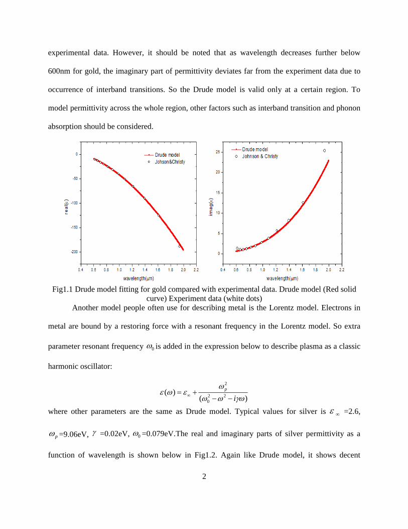
experimental data. However, it should be noted that as wavelength decreases further below
600nm for gold, the imaginary part of permittivity deviates far from the experiment data due to
occurrence of interband transitions. So the Drude model is valid only at a certain region. To
model permittivity across the whole region, other factors such as interband transition and phonon
absorption should be considered.
Fig1.1 Drude model fitting for gold compared with experimental data. Drude model (Red solid curve) Experiment data (white dots)
Another model people often use for describing metal is the Lorentz model. Electrons in
metal are bound by a restoring force with a resonant frequency in the Lorentz model. So extra
parameter resonant frequency 0ω is added in the expression below to describe plasma as a classic
harmonic oscillator:
2
2 20
( )( )
p
i
ωε ω ε
ω ω γω∞= +− −
where other parameters are the same as Drude model. Typical values for silver is ε ∞ =2.6,
pω =9.06eV, γ =0.02eV, 0ω =0.079eV.The real and imaginary parts of silver permittivity as a
function of wavelength is shown below in Fig1.2. Again like Drude model, it shows decent

3
agreement with experimental data over the range from 600nm to 2000nm. However, here I only
use tail part of Lorentz model to fit a certain range of permittivity by setting a low resonant
frequency. So the interband transitions which take place in high frequency range are not
considered here.
Fig1.2 Lorentz model fitting for silver compared with experimental data
To fully capture the optical response in the wide range, a combination of these two, the
Lorentz-Drude model was frequently used by people. In the model, the Drude model and the
Lorentz model account for the free electrons effect and interband transition respectively. The
Drude-Lorentz model is given by the following equation:
2 20
2 210
( ) 1( ) ( )
kp j p
j j j
f f
i i
ω ωε ω
ω ω ω ω ω=
= − +− Γ − + Γ∑
where pω is plasmon frequency, 0Γ and 0f are damping constant and strength associated with
free electron model, k is the number of oscillators with frequency jω ,strength jf and damping
constant for Lorentz model. It is important to note here that the model should be carefully chosen
depending on what range of wavelength you are interested in. For example, although the full

4
model can give me a good fitting across the whole range, I will use the simple Drude model for
most of my simulation in the thesis since no interband transitions happen in my wavelength
interest. For some other part of my simulation, interpolation of experimental data is used for
describing wavelength dependent of silver permittivity.
However, there are some drawbacks for metal being a perfect plasmonic material. Single
wavelength range of plasmonic resonance, incompatibility with semiconductor manufacturing
process and high metal loss limit it for being an ideal building block in a plasmonic-based system
[2]. To avoid these intrinsic disadvantages, efforts on finding new substitutes never stop. Doped
semiconductor is probably one of those substitutes, because the complex permittivity of it is very
similar to that of the metal at near optical frequency, except that the effective mass of the
electrons for the n-type doped semiconductors or the holes for p-type doped semiconductors
have to be used [3]. By increasing the doping concentration, the optical response of highly doped
semiconductor can behave like metal at a desirable wavelength range. Typically, for III-IV
heavily doped semiconductors, metallic behavior happens at mid infrared range depending on
achievable doping concentration. Thus, it is interesting to investigate the optical response of
doped semiconductor for possible plasmonic application. Here I use a combination of Adachi’s
model and Drude model to analyze the permittivity of heavily doped InAs with different doping
concentrations. The Adachi’s model [4] which adopted critical points transition approach was
applied here to account for interband transitions while the Drude model is responsible for the
free carrier effect. The expression for permittivity is given:
2
2( ) p
r b i
ωε ω ε
ω γω= −
+

5
where 2
2*
0p
Nq
mω
ε= , bε is dielectric constant related to interband transition, which as mentioned
earlier can be calculated by the Adachi’s model. It should be noted here Adachi’s model is only
valid for lightly or undoped semiconductor. To fully consider the effect of doping on the
absorption, 0( )v cf fα α= − is used where α and 0α represent absorption coefficient for heavily
doped and undoped semiconductor respectively. fv, fc are the Fermi-Dirac distributions for the
electrons in the valence band and in the conduction band. Usually the values of fv, fc are set to be
1 and 0 for undoped semiconductor as the valence band is completely occupied and the
conduction band is empty. For highly doped semiconductors, the case is different as the
absorption edge is pushed to higher energy due to populated state at the bottom of conduction
band, which is a famous phenomenon called Burstein-Moss effect. The fv –fc as a function of
energy for InAs at different doping concentrations are shown in Fig1.3. Clear band gap shift can
be observed from the figure. After considering the doping effect on the absorption,α is
connected with the imaginary part of dielectric function by 2bn cα
εω
= where c is speed of light
and bn is the background refractive index. For the Drude model part, the parameters are adopted
from experimental data [5] measured by UIUC group. Until now, the whole dielectric function
model has been proposed and results are shown in Fig1.5 and Fig1.6. As can been from the
figures, each contribution part dominates at different spectral regions. At Mid IR region, free
electrons effect contributes most such that real part of permittivity can reach negative .From
Fig1.4, tunability of transition energy for real part of permittivity becoming negative is shown.
This doping dependent relationship enables people to explore plasmonic effect of highly doped
semiconductor at a desirable wavelength range if assuming any effective heavy doping level is
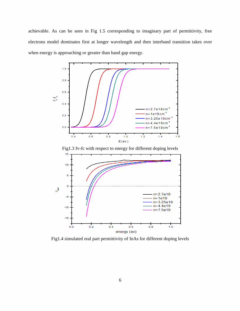
6
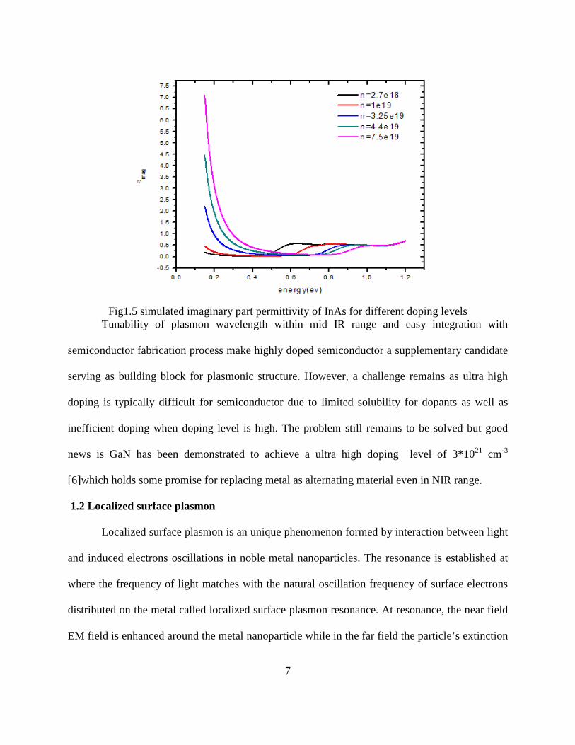
achievable. As can be seen in Fig 1.5 corresponding to imaginary part of permittivity, free
electrons model dominates first at longer wavelength and then interband transition takes over
when energy is approaching or greater than band gap energy.
Fig1.3 fv-fc with respect to energy for different doping levels
Fig1.4 simulated real part permittivity of InAs for different doping levels
7
Fig1.5 simulated imaginary part permittivity of InAs for different doping levels Tunability of plasmon wavelength within mid IR range and easy integration with
semiconductor fabrication process make highly doped semiconductor a supplementary candidate
serving as building block for plasmonic structure. However, a challenge remains as ultra high
doping is typically difficult for semiconductor due to limited solubility for dopants as well as
inefficient doping when doping level is high. The problem still remains to be solved but good
news is GaN has been demonstrated to achieve a ultra high doping level of 3*1021 cm-3
[6]which holds some promise for replacing metal as alternating material even in NIR range.
1.2 Localized surface plasmon
Localized surface plasmon is an unique phenomenon formed by interaction between light
and induced electrons oscillations in noble metal nanoparticles. The resonance is established at
where the frequency of light matches with the natural oscillation frequency of surface electrons
distributed on the metal called localized surface plasmon resonance. At resonance, the near field
EM field is enhanced around the metal nanoparticle while in the far field the particle’s extinction

8
spectrum has maximum peak due to cancellation of induced field and incoming field. To
investigate how the EM field near the metal is enhanced, a simulation on the three silver
nanoparticles system is performed by CMOSOL Multiphysics 4.2a. For a better comparison,
pure dielectric systems with different permittivity which adopt an index confining mechanism
are given as a contrast shown in Fig1.6.The incident light is from the top with polarization
parallel to inter-particle axis with amplitude of 1 V/m.
Fig1.6 Three different configurations for field enhancement study
The maximum field intensity inside the system with respect to wavelength is shown in
Fig.1.7. Red and black curves stand for pure dielectric nanoparticles system with different
dielectric constants while green curve is for metallic one. The peak of it represents where the
resonance is with inset showing the field distribution at resonance. As can be seen from the
figure, the metallic plasmonic system is far superior to conventional dielectric system in ability
to enhance field whether it’s on resonance or not. This great enhancement of field by metal

9
nanoparticles can find application in biosensing, especially in the Surface Enhanced Raman
scattering (SERS) technique.
Fig1.7Maximum field intensity for different configurations with respect to wavelength Green
color represents metal particles, Red color represents dielectric particles with permittivity of 10 and black color stands for dielectric particles with permittivity of 3.
Another method to determine the Localized surface plasmon resonance is to calculate the
extinction spectral in the far field for metallic nanoparticles. The resonances occur at where the
extinction spectral peaks. The Lumerical software based on FDTD simulation is used to
investigate the optical response of metallic particles. Extinction cross section, scattering cross
section and absorption cross section are calculated by the software for single gold nanoparticle in
Fig1.8.Here the scattering cross section is defined as collected power in the far field normalized
by intensity of incident light and absorption cross section is calculated by total power absorbed
by particle in the near field divided by incident intensity, then the extinction cross section is a
sum of these two. As can be seen from figure, local surface plasmon resonance occurs at around

10
500 nm for gold particle with a size of diameter 50nm and inset shows near field distribution at
resonance. It’s interesting to note that absorption process dominates for small size one as most of
light is absorbed rather than scattered due to much smaller diameter than the wavelength of light.
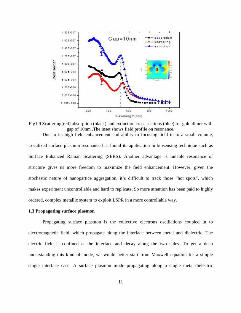
The following figure 1.9 gives the same plot but for gold dimmer with a 10 nm separation. Here
it's worth to point that LSPR of nanostructure depends on a lot of factor such as shape, size,
aspect ratio of structure and embedding environment.
Fig1.8 Scattering (red) absorption (black) and extinction cross sections (blue) for gold particle with a diameter of 50nm .The inset shows field profile on resonance.
11
Fig1.9 Scattering(red) absorption (black) and extinction cross sections (blue) for gold dimer with gap of 10nm .The inset shows field profile on resonance.
Due to its high field enhancement and ability to focusing field in to a small volume,
Localized surface plasmon resonance has found its application in biosensing technique such as
Surface Enhanced Raman Scattering (SERS). Another advantage is tunable resonance of
structure gives us more freedom to maximize the field enhancement. However, given the
stochastic nature of nanopartice aggregation, it’s difficult to track those “hot spots”, which
makes experiment uncontrollable and hard to replicate, So more attention has been paid to highly
ordered, complex metallic system to exploit LSPR in a more controllable way.
1.3 Propagating surface plasmon
Propagating surface plasmon is the collective electrons oscillations coupled in to
electromagnetic field, which propagate along the interface between metal and dielectric. The
electric field is confined at the interface and decay along the two sides. To get a deep
understanding this kind of mode, we would better start from Maxwell equation for a simple
single interface case. A surface plasmon mode propagating along a single metal-dielectric

12
interface is shown in Fig 1.10.Actually in order to be supported by this structure, the surface
plasmon mode has to be TM mode in nature with (Ex,Hy,Ez) components.
Fig1.10 surface plasmon polariton propagates along the single Metal-Dielectric interface The electric and magnetic fields for a surface plasmon polariton which propagates along
the x direction and decays along the z direction must take the following form:
( )
( )
( )
( )
(0, , 0)
(E , 0, E )
(0, , 0)
(E , 0, E )
xd zd
xd zd
xm zm
xm zm
i k x k z td yd
i k x k z td xd zd
i k x k z tm ym
i k x k z td xm zm
H H e
E e
H H e
E e
ω
ω
ω
ω
+ −
+ −
+ −
+ −
=
=
=
=
where subscripts d,m represent dielectric and metal respectively, zdk , zmk means z component of
wavevectors at dielectric part and metal part,xd md xk k k= = stands for x component of
wavevector along the interface. By matching the boundary conditions in which Hy and Dz are
continuous and substituting field equations in to Helmholtz equation 2 2 0E k E∇ + =ur ur
, we obtain
the following relation:
2
2 22
m d
z m z d
x z i i
k k
k kc
ε ε
ωε
=
+ =

13
where i denotes either metal part or dielectric part, ε is permittivity of medium,ωmeans angular
frequency of light, c is the speed of light. Combing those two equations, the dispersion relation
of surface plasmon polariton can be given:
2 20
22 2
0
m dx
m d
iz i
m d
k k
k k
ε εε ε
εε ε
=+
=+
The fig1.11 shows energy dispersion of surface plasmon polariton for silver–air interface. Red
curve means analytic results which agree pretty well with simulation results represented by white
dots. As can be seen from the figure, the propagating wavevector increase massively when
energy increases, which means the effective wavelength propagating along the interface
decreases correspondingly at high energy. At some point where the wavevector attains the
maximum, the surface plasmon resonance is achieved. One thing not shown but should be noted
that if increasing the energy further ,the dispersion curve would reflect back to small
wavevectors region due to ohmic loss present in the metal.
Fig 1.11 Energy dispersion relationship of surface plasmon for single Ag-air interface As discussed above in the single interface case, wavelength in the medium can be
shrinked massively in the propagation direction, which opens a possibility to squeeze light

14
energy in a very ultrasmall area. Another important structure supporting propagating surface
plasmon called Metal-Semiconductor-Metal (MIM) structure. MIM, as name indicates, consists a
dielectric core sandwiched by two metal slab given in Fig1.12.The propagation direction is along
x direction.
Fig1.12 Surface plasmon polariton propagates in MIM waveguide (symmetric case) Actually we can view it as two single metal-dielectric cases interacting with each other.
When d is too large for two surface plasmons to interact, no coupling effect happens. As d is thin
enough, then interaction between two single interface surface plasmons occurs. The smaller
distance between two metal slabs, the stronger interaction it has. The effect of interaction would
lead a splitting of mode in to two .one is symmetric mode, the other is antisymmetric one with
different phases of charge oscillation distributed on the metal surface. Here the symmetry is
defined as Ez with respect to the middle of dielectric layer. It’s worth noting that although two
kinds of modes exist in this structure, it’s difficult to excite antisymmetric mode in the real
practice due to field symmetry. Thus, we discuss only the symmetric case hereafter. The 2D
FDTD simulation was performed on this structure with uniform in the y direction. A dipole was
put at the entrance of MIM to excite plasmonic mode and d was set thinner than 100nm for

15
strong interaction. The dominant electric field Ez and magnetic field Hz distribution is shown in
Fig1.13.The thickness of dielectric layer here is 20 nm.
Fig1.13 Ez field distribution (Left)and Hy field distribution(right) for symmetric mode
As can be seen from the figure, the field energy is squeezed in to thin dielectric region
with thickness far below the diffraction limit, which opens a possibility to realize subwavelength
guiding utilizing this mode. To further understand the property of this mode, the energy
dispersions for different thickness and different dielectric medium are given respectively in
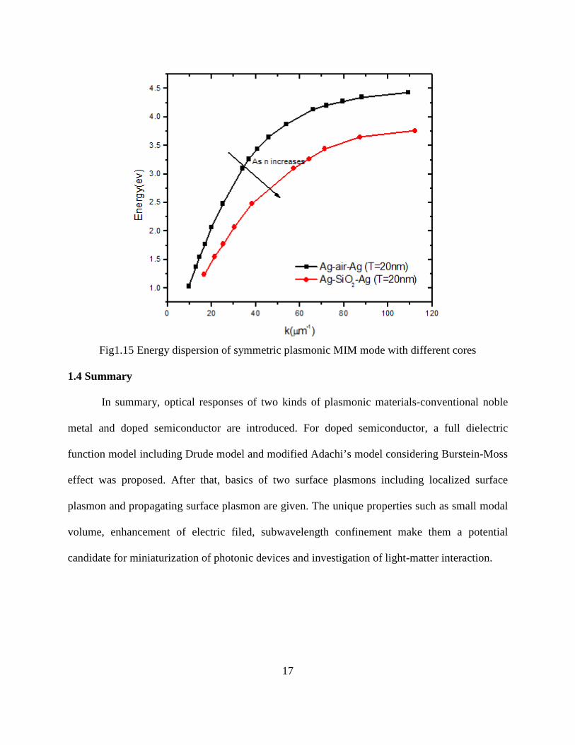
Fig1.14 and Fig.1.15.All of the curves asymptotically approach some certain energy values just
like single interface case does, which is actually a common feature for energy dispersion of
surface plasmonic mode. Those certain values correspond to different resonance energy of
modes. From Fig1.14, as the thickness of dielectric decreases from 20nm to 5nm, the dispersion
curve becomes flat meaning that the smaller wavelength of plasmon can be obtained for the same
free space wavelength in the thinner waveguide (dielectric region). That’s understandable since
the interaction is much stronger in thinner one, leading a further exploration of plasmonic effect
in the waveguide. In theory, the thickness can be indefinitely small and good news is current
technology has enabled deposition of nanometer-thick film. Miyazaki [7] has achieved
experimentally to squeeze visible light in to 3nm thick nanocavity with this kind of mode, which
proved that utilizing plasmonic mode to achieve ultra-small nanocavity was feasible. In Fig1.15,
dispersion curves for different dielectric mediums are given. As clearly can be seen, the

16
resonance energy for high index medium is lower that for low index one and MIM with high
index core can enable better shrinking of light in visible wavelength range. As a consequence,
much attention has been paid in to metal-semiconductor-metal structure with both gain available
and high compression of light to achieve active waveguides and lasers.
Fig1.14 Energy dispersion of symmetric plasmonic MIM mode at different thickness
17
Fig1.15 Energy dispersion of symmetric plasmonic MIM mode with different cores
1.4 Summary
In summary, optical responses of two kinds of plasmonic materials-conventional noble
metal and doped semiconductor are introduced. For doped semiconductor, a full dielectric
function model including Drude model and modified Adachi’s model considering Burstein-Moss
effect was proposed. After that, basics of two surface plasmons including localized surface
plasmon and propagating surface plasmon are given. The unique properties such as small modal
volume, enhancement of electric filed, subwavelength confinement make them a potential
candidate for miniaturization of photonic devices and investigation of light-matter interaction.

18
CHAPTER 2
PLASMONIC WAVEGUIDES
2.1 Insulator-metal-insulator waveguide
The plasmonic waveguide is a potential candidate for future chip communication due to
subwavelength confinement far beyond the diffraction limit, which enables its integration with
electronic transistors. Thus, numerous plasmonic waveguides with different configurations
utilizing surface plasmon polariton attract people’s interest. Of them, two prototype planer
structures which are the metal film (Insulator-metal-insulator) and the metal gap (metal-
insulator-metal) waveguide receive more attention than others due to suitability for nano-optical
integrated circuits [8,9].The structure of IMI is given in Fig2.1.
Fig2.1The cross section view of metal film embedded in dielectric
Fig.2.1 shows a cross section view of an infinite metal film embedded in the dielectric
environment and propagation is along the direction perpendicular to the paper. Suppose the
superstrate is the same as substrate, then this structure supports two kinds of modes, as MIM
waveguide does. One is symmetric mode, which is also called Long-Range Surface Plasmon

19
Polariton (LRSP). The other mode is antisymmetric, namely Short-Range Surface Plasmon
Polariton (SRSP). The symmetry here is defined with respect to Ex field. As name indicated, the
LRSP has longer propagation length than the SRSP mode. It should be noted here that LRSP
doesn’t exist if the substrate is different from the superstrate due to break of symmetry. The Ex
field distribution of two kinds of modes with metal thickness of 20nm at communication
wavelength 1.55um is shown in Fig2.2.Here the silver is embedded in the dielctric(SiO2)in the
simulation.
Fig2 .2 Ex field distribution for (a) SRSP and (b) LRSP
The effective index of two modes with respect to metal thickness at 1.55um is given in
Fig2.3. As can be seen from the figure, when the metal thickness is relatively large, two surface
plasmons propagate along each interface separately without interaction. So the effective
refractive indexes for SRSP and LRSP are identical. As the thickness decreases, surface
plasmons couple with each other , which leads to a splitting of mode in to the symmetric and

20
antisymmetric one. The upper branch, representing the antisymmetric mode, increases
dramatically with the decreasing thickness while the lower branch approaches the permittivity
value of dielectric, meaning the propagating mode is still bound at interface. Both of them show
no cutoff with respect to thickness of the metal layer. As can be seen from Fig2.2, the SRSP
mode is tightly bound to the metal surface, which results in a stronger modal confinement than
that of LRSP. This point can also be reflected in increasing effective refractive index for SRSP in
the Fig2.3. In order to compare two kinds of modes in transmission characteristics, the
propagation loss of each mode is shown in Fig2.4. The propagation loss of SRSP dramatically
increases with the decreasing thickness, while that of LRSP decreases massively showing itself a
potential candidate for chip communication. Combined with results obtained from Fig2.3, we
can conclude now SRSP has a strong confinement with a short propagation length whereas LRSP
owns a long propagation length but with poor modal confinement. Although we can’t combine
these advantages into one mode, we can selectively excite either mode we prefer to use
according to different applications. For example, we can use SRSP for nano-focusing or nano-
guiding to confine light energy in to ultra-small area and adopt LRSP mode for chip
communication and long range transmission. So far the selective mode excitation as well as
mode convertor has been experimentally demonstrated by two phase controlled beams or
theoretically investigated in order to get flexibility in benefiting from two opposing
characteristics [10-12].

21
Figure 2.3 Effective index of two propagation modes as a function of thickness at 1.55um
Figure 2.4 Propagation loss of two propagation modes as a function of thickness at 1.55um

22
In the previous part, we talked about the case for infinite metal stripe embedded in
dielectric matrix, next we will discuss finite width case of IMI waveguide. For simplicity, a
silver nanowire waveguide, which can be viewed as an IMI waveguide along any direction, is
analyzed in the simulation. The structure consists of a silver nanowire embedded in the silicon
dioxide with its cross-section view given in Fig2.5(a) .The propagation direction is again
perpendicular to the paper. Unlike the modes supported by infinite metal stripe, modes here are
not purely TM modes and have all six field due to finite width[12], so we term these modes
SRSP-like and LRSP-like modes with electric field distribution given in Fig2.5(b) and Fig2.5(c)
respectively.
Fig2.5(a) Cross sectional view of silver nanowire embedded in SiO2 matrix (b)Norm of
electric field for SRSP-like mode(c) for LRSP-like mode
The effective refractive index of two modes is shown in Fig2.6 as a function of radius at a
vacuum wavelength of 600 nm. Similar to the case with infinite width, the upper branch, which
stands for SRSP, goes infinitely with the decreasing radius while the lower branch is decreasing
slowly. However, one major difference is that there is a cut off for LRSP-like mode in silver
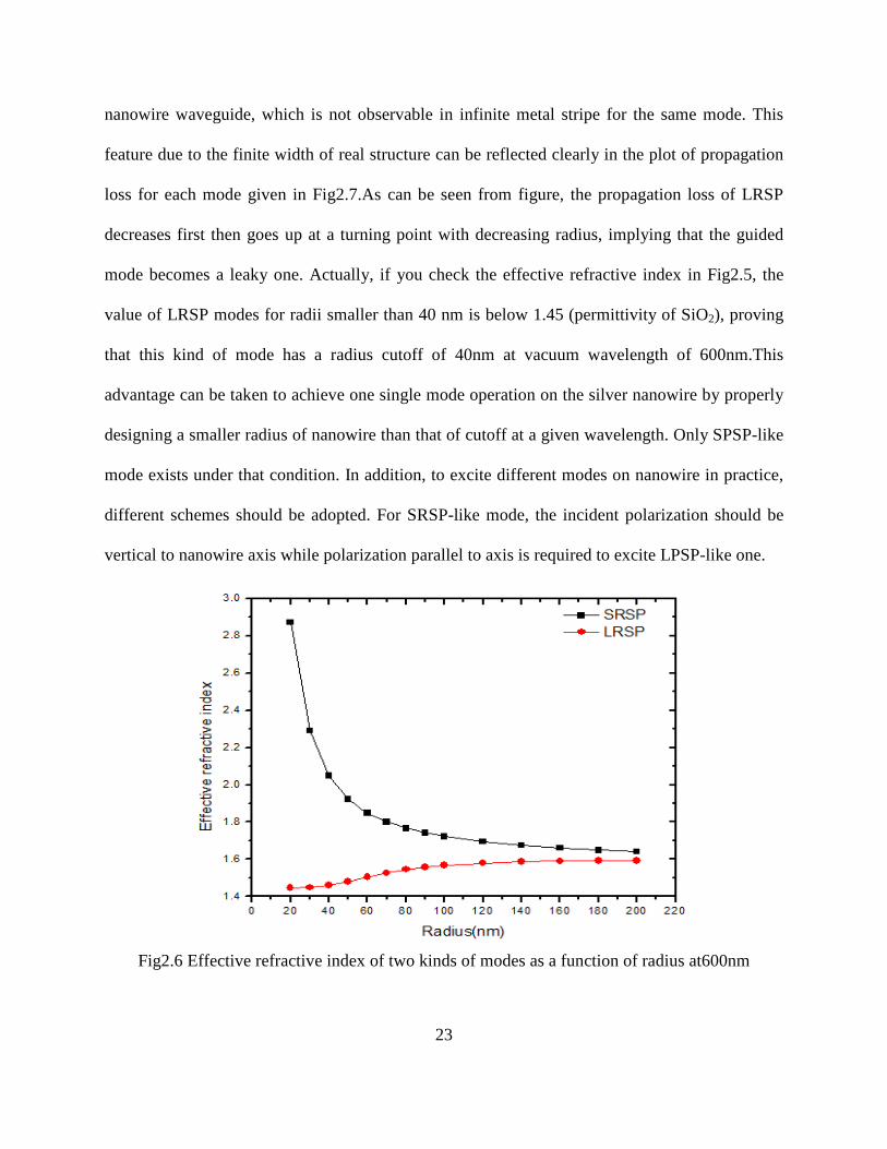
23
nanowire waveguide, which is not observable in infinite metal stripe for the same mode. This
feature due to the finite width of real structure can be reflected clearly in the plot of propagation
loss for each mode given in Fig2.7.As can be seen from figure, the propagation loss of LRSP
decreases first then goes up at a turning point with decreasing radius, implying that the guided
mode becomes a leaky one. Actually, if you check the effective refractive index in Fig2.5, the
value of LRSP modes for radii smaller than 40 nm is below 1.45 (permittivity of SiO2), proving
that this kind of mode has a radius cutoff of 40nm at vacuum wavelength of 600nm.This
advantage can be taken to achieve one single mode operation on the silver nanowire by properly
designing a smaller radius of nanowire than that of cutoff at a given wavelength. Only SPSP-like
mode exists under that condition. In addition, to excite different modes on nanowire in practice,
different schemes should be adopted. For SRSP-like mode, the incident polarization should be
vertical to nanowire axis while polarization parallel to axis is required to excite LPSP-like one.
Fig2.6 Effective refractive index of two kinds of modes as a function of radius at600nm

24
Fig2.7 Propagation loss for SRSP and LRSP with respect of radius at wavelength of 600nm
To further explore substrate effect on the propagating modes, silver nanowire on the
substrate (embedded in an asymmetric dielectric) is studied with cross section view given in
Fig2.8(a).Unlike the nanowire without substrate, It can only support SRSP-like mode
(asymmetric) due to break of symmetry with respect to Y=0 cutline in the Fig2.7.The field
distribution of a guiding SRSP-like mode is shown in Fig2.8(b) with a saturated color bar used.
We can observe much more field concentrates in the SiO2 side than that in air side due to the
substrate drawing effect. However, leaking issue might become severe at a certain wavelength
range where the effective refractive index is smaller than the permittivity of SiO2 and
propagation loss dramatically increases. Fig2.8(c) gives a field distribution of a leaking SRSP-
like mode and effective index with respect to wavelength for radius of 45nm and 50nm is
provided as well in Fig2.9. As can be seen from the figure, the cutoff wavelength for radius of
45nm and 50nm is 921nm and 826nm, respectively, which means that the operation wavelength

25
cannot exceed 921nm and 826nm for radius of 45nm and 50nm to achieve mode guiding. Thus,
the introduction of a different substrate to supersubstrate imposes a new cutoff condition on the
radius of nanowire and operation wavelength for SRSP-like mode.
Fig2.8 Cross sectional view of silver nanowire on SiO2 substrate (b) Norm of electric field for
SRSP-like guiding mode(c) for leaking mode
Fig2.9 Effective refractive index of SRSP-like mode versus wavelength for different nanowires

26
2.2 Metal-Semiconductor-Metal waveguide
In the last section, we talked about one prototype IMI waveguide and particularly one
appealing application in nanowire form. For this section, another important plasmonic
waveguide, namely Metal-Semiconductor-Metal waveguide (MSM) will be discussed in terms of
modes characteristics. We have given an introduction to surface plasmon polariton in 2D MIM
structure in the last chapter, showing its unique ability to manipulate light in nanosacle. Hereafter
we focus mainly on the propagation characteristics for both symmetric mode and antisymmetric
mode in the infinite long waveguide structure. Fig2.10 gives a cross sectional view of MSM
structure with propagation direction in Z direction. Semiconductor core GaAs with refractive
index 3.59 is used in the simulation.
Fig2.10 Cross sectional view of MSM waveguide with infinite width
As the same analogy IMI waveguide has, this structure can be treated as two separately
propagating Metal-Semiconductor waveguide as well. With thickness of core layer t is below to
certain level, the interaction of vertical surface plasmons occurs which lead to a splitting of
single mode in to symmetric case and antisymmetic case. Here the thickness is fixed at100nm
where the interaction is occurring .The field distribution of each mode at vacuum wavelength
650nm is given in Fig2.11. As can be seen from the figure, the electric field component Ex
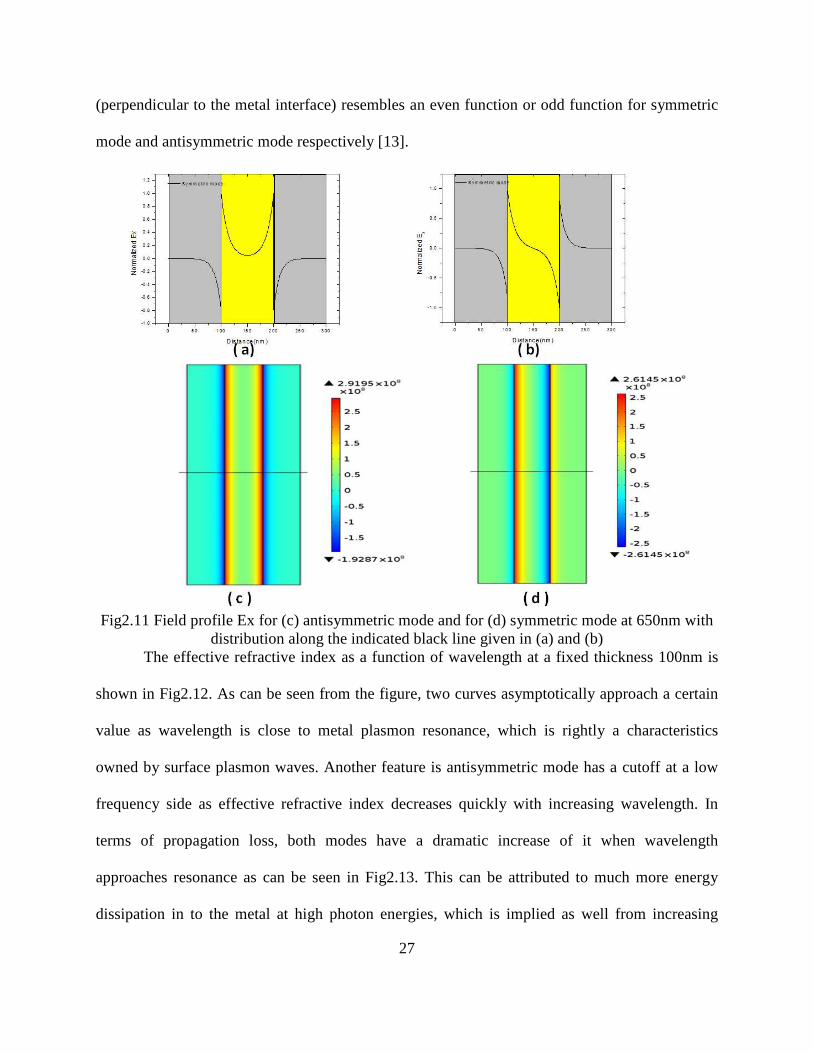
27
(perpendicular to the metal interface) resembles an even function or odd function for symmetric
mode and antisymmetric mode respectively [13].
Fig2.11 Field profile Ex for (c) antisymmetric mode and for (d) symmetric mode at 650nm with
distribution along the indicated black line given in (a) and (b) The effective refractive index as a function of wavelength at a fixed thickness 100nm is
shown in Fig2.12. As can be seen from the figure, two curves asymptotically approach a certain
value as wavelength is close to metal plasmon resonance, which is rightly a characteristics
owned by surface plasmon waves. Another feature is antisymmetric mode has a cutoff at a low
frequency side as effective refractive index decreases quickly with increasing wavelength. In
terms of propagation loss, both modes have a dramatic increase of it when wavelength
approaches resonance as can be seen in Fig2.13. This can be attributed to much more energy
dissipation in to the metal at high photon energies, which is implied as well from increasing

28
effective index. It should be noted here that the propagation loss for symmetric mode is
decreasing consistently until to a certain level with the increasing wavelength while the loss for
antisymmetric mode would decrease first then increase after that due to cut off of the mode as
can be seen in the inset of the figure plotted in the logarithm scale.
Fig2.12 Effective refractive index as function of wavelength for t=100nm
Fig2.13 Propagation loss versus wavelength for t=100nm
29
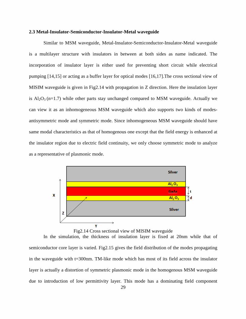
2.3 Metal-Insulator-Semiconductor-Insulator-Metal waveguide
Similar to MSM waveguide, Metal-Insulator-Semiconductor-Insulator-Metal waveguide
is a multilayer structure with insulators in between at both sides as name indicated. The
incorporation of insulator layer is either used for preventing short circuit while electrical
pumping [14,15] or acting as a buffer layer for optical modes [16,17].The cross sectional view of
MISIM waveguide is given in Fig2.14 with propagation in Z direction. Here the insulation layer
is Al2O3 (n=1.7) while other parts stay unchanged compared to MSM waveguide. Actually we
can view it as an inhomogeneous MSM waveguide which also supports two kinds of modes-
antisymmetric mode and symmetric mode. Since inhomogeneous MSM waveguide should have
same modal characteristics as that of homogenous one except that the field energy is enhanced at
the insulator region due to electric field continuity, we only choose symmetric mode to analyze
as a representative of plasmonic mode.
Fig2.14 Cross sectional view of MISIM waveguide
In the simulation, the thickness of insulation layer is fixed at 20nm while that of
semiconductor core layer is varied. Fig2.15 gives the field distribution of the modes propagating
in the waveguide with t=300nm. TM-like mode which has most of its field across the insulator
layer is actually a distortion of symmetric plasmonic mode in the homogenous MSM waveguide
due to introduction of low permittivity layer. This mode has a dominating field component

30
perpendicular to the metal surface(X direction) which is a nature for surface plasmon waves. The
other mode with most of energy confined in the semiconductor core has dominating field along
the Y direction and little electric field component in Z direction. So we call this mode TE-like
mode.
Fig2.15 (a) Norm of electric field distribution along the black line indicated at (b) TM-like
mode and (c) TE-like mode The effective refractive index and propagation loss for each mode as a function of
semiconductor core width at vacuum wavelength 800nm are shown in Fig2.16.The red square
represents TE- like mode while black cube stands for TM-like mode with effective index and
propagation loss indicated in the left and right axis separately. As can be seen from the figure,
the TE mode sees a cut off around 100nm (roughly diffraction limit) as indicated by dramatically
increased propagation loss and massively decreased effective index. For TM-like mode, the
effective index decreases flatly with the decreasing of core width showing a possibility of
indefinite shrinking of semiconductor width in theory. However, the propagation loss is
increased significantly with the decrease of width, meaning much larger gain is required to
achieve lossless propagation at the smaller width far beyond the diffraction limit.

31
Fig2.16 Effective refractive index and propagation loss for TM-like mode and TE-like mode
versus semiconductor core with at 800nm 2.4 Summary
Plasmonic waveguides of different configurations and geometries are investigated in this
chapter. Modal characteristic for each waveguide is given. For IMI waveguide, there are two
propagating modes due to coupling of two single surface plasmons , which results in different
phases of charge oscillations. One is antisymmetric mode (SRSP) with strong confinement
capability and relatively low propagation length while the other one is symmetric mode (LPSP)
which has poor confinement capability and long propagation loss. This kind of mode splitting
phenomena is observed as well in nanowire waveguide and MSM waveguide. In contrast to IMI
waveguide which has no cutoff for both modes, nanowire waveguide has radius cutoff for
symmetric mode arising from finite width and a wavelength cutoff for only-propagating
antisymmetric mode in the case with substrate. High energy mode in MSM waveguide shows
frequency cutoff as well. Lastly, a comparison of TM-like and TE-like mode in MISIM
waveguide shows potential of plasmonic mode in shrinking the width.

32
CHAPTER 3
PLASMONIC NANOLASER
3.1 Metal-Semiconductor-Metal nanolaser cavity
Previously we talked about different plasmonic waveguides using surface plasmon
polariton which affords a unique ability to confine light in subwavelength scale. In this chapter,
we focus on this feature employed on the nanolaser. The miniaturization of laser has been an
ever-increasing demand for community since there is still a size mismatch between electronic
device and photonic device .In order to combine these two in one chip with high dense
integration, one must shrink photonic device such as lasers to the size comparable to electronic
transistors for on-chip communication.
Recently metal has been playing an important role to achieve the subwavelength
confinement to further shrink laser cavity. Generally there are two different approaches with the
same metal cladding. One is use metal-optic cavity to confine optical mode as demonstrated in
[18,19].In this case ,the metal serves as only an efficient reflector as it always does in microwave
community. The mode can be confined well with reduced radiation loss and modal volume. The
other case is to utilize truly surface plasmon to confine light as demonstrated in [20-23] .Using of
plasmonic mode can break diffraction limit and make an ultra-small laser in three dimensions.
However, it would subject to severe metal loss due to strong interaction between electrons and
photons. Normally the cavity of optical mode requires larger dimension than plasmonic mode
while the plasmonic mode has larger loss than optical mode.
To examine quantitatively the cavity performance of two modes such as quality factor,
modal volume and threshold gain, we investigate a prototype metal-semiconductor-metal cavity
shown in Fig3.1 which can support plasmonic mode and optic mode simultaneously in the
33
infrared regime. Similar to metal-semiconductor-metal waveguide, the cavity consists of
semiconductor disk sandwiched by two metal disks. The semiconductor disk is used to provide
gain and metal disks serve as either a reflective mirror or source for electrons coupled in to
plasmonic mode to achieve confinement.
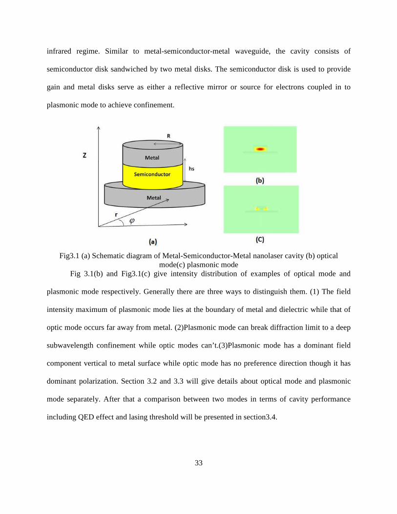
Fig3.1 (a) Schematic diagram of Metal-Semiconductor-Metal nanolaser cavity (b) optical
mode(c) plasmonic mode Fig 3.1(b) and Fig3.1(c) give intensity distribution of examples of optical mode and
plasmonic mode respectively. Generally there are three ways to distinguish them. (1) The field
intensity maximum of plasmonic mode lies at the boundary of metal and dielectric while that of
optic mode occurs far away from metal. (2)Plasmonic mode can break diffraction limit to a deep
subwavelength confinement while optic modes can’t.(3)Plasmonic mode has a dominant field
component vertical to metal surface while optic mode has no preference direction though it has
dominant polarization. Section 3.2 and 3.3 will give details about optical mode and plasmonic
mode separately. After that a comparison between two modes in terms of cavity performance
including QED effect and lasing threshold will be presented in section3.4.
34
3.2 optical modes
The optical modes supported in the above structure can be obtained by assuming metal as
a perfect electrical conductor(PEC) and semiconductor side wall as a perfect magnetic
conductor(PMC).This approximation which is excellent in microwave regime can also be
adopted here in near-infrared region to capture profiles and symmetries of the cavity modes
since no surface plasmons exist in this region for optical mode[24].Thus, in terms of eigenmodes
function, we can borrow an idea from micro-patch antenna which is the bigger version of above
structure. The notation TEmnp and TMmnp is used to specify particular mode for this cavity, where
m,n,p represent azimuthal, radial and axial modal numbers. The fundamental TM mode and TE
mode are TM110 and TE011 mode respectively .However, TM110 mode is the mode of choice of
circular micropatch antennas at RF/microwave frequencies [25] as an efficient radiator and not
suitable for laser application, here we refer TM111 and TE011 as the most fundamental TM mode
and TE mode with their field profiles given in cylindrical coordinates below:
1 1 1
1 1 1
1 1 1
1 1 1
1 1 1 1 1 1
0 1 1 0 1 1
1 1 1
0 1 ,
'0 1 ,
,
,0
, ,
0 1 1
20 , 0 ,
:
( , , ) ( k ) c o s ( ) s i n ( )
( , , ) J ( k ) s i n ( ) s i n ( )k
( k )( , , ) s i n ( ) c o s ( )
k k
T E :
( , , ) k ( k ) c o s
z r T M
r r T Mr T M
m r T M
r T M r T M
z r T E r T E
T M
E r z E J r zh
E r z E r zh h
J rE r z E z
h r h
H r z H J r
φ
πφ φ
π πφ φ
π πφ φ
φ
= −
= −
= −
= −
0 1 1
0 1 1
0 1 1 0 1 1
, '0 0 ,
'0 , 0 ,
( )
k( , , ) J ( k ) c o s ( )
( , , ) k J ( k ) s i n ( )
H ( , , ) ( , , ) ( , , ) 0
r T Er r T E
r T E r T E
z r
zh
H r z H r zh h
E r z i H r zh
r z E r z E r z
φ
φ
π
π πφ
πφ ω µ
φ φ φ
=
=
= = =
where 2 2 2( / ) ( / )r mnpk c hω ε π= − , h is cavity height , mnpω is cavity resonance frequency and ε is
the permittivity of semiconductor medium. FDTD Simulation is performed by MIT made
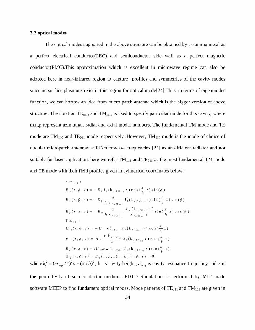
software MEEP to find fundament optical modes. Mode patterns of TE011 and TM111 are given in
35
Fig3.2. Each component of electric field which is not shown here also agrees well with analytic
equations. One thing should be noted here different source polarizations are required to excite
different modes due to match of field distribution.
Fig3.2 Field intensity
2E for (a) TM111 mode and (b) TE011mode
Although no surface plasmon is involved in this optical mode, there is still interaction
between metal and electromagnetic mode which confine light into a small modal volume with a
decent Q. Simulation shows for a cavity with height 230 nm and radius 250nm,TM111 has a
modal volume 30.5( )2n
λ and Q is 250 while TE011 has a modal volume of 32.9( )
2n
λ with Q about
143.Of them TM111 is considered as the most potential mode in lasing application since it
represents the most fundamental moderate Q mode with a subwavelength modal volume .In the
section 3.4, we will use this mode as a representative of optical mode to make a full comparison
with plasmonic mode which is supported in this structure as well .

36
3.3 Plasmonic mode We discussed in the last section about optical modes which are diffraction limited. In
order to further shrink the device far beyond the limit, surface plasmon modes must be employed
to achieve deep-subwavelength confinement owing to its unique property in manipulating light at
nanoscale. In this metal-semiconductor-metal laser cavity, surface plasmons can be formed in the
semiconductor region like that propagating in the MSM waveguide we talked earlier. The
coupling between two metal-semiconductor interface leads to the splitting of mode in to two
(symmetric and antisymmetric). Antisymmetric mode has a wavelength cutoff and difficult to
excite due to metal skin effect, thus the focus of plasmonic mode is on symmetric one. The
dispersion relationship for symmetric mode is given in the following:
tanh( / 2)m d d d mk k t kε ε= −
where 2
2 22d spp mk k
c
ωε= − ,
22 2
2m spp dk kc
ωε= − .Simulation did in the section1.3 shows MSM
plasmonic mode has much larger wavevector or momentum as wavelength approaches
resonance wavelength or the thickness of semiconductor is become thin. The high momentum
enables more possibility of the mode to undergo internal reflection around disk circumference
with necessary feedback forming whispering gallery (WG) plasmonic mode. The resonance
condition of whispering gallery mode is given:
( 1,2,3,...)sppk R m m= =
where sppk is the wavevector of plasmonic mode, R is the radius of disk, and m is an integer. It’s
clear to see here that since kspp increases with the decrease of thickness in vertical direction, R in
the planar direction should be decrease as well to maintain at the same wavelength. This provides
an opportunity to achieve full three-dimensional subwavelength confinement as discussed in [26,
27].we will present this point in details later with simulation results. The WG mode profile with

37
an azimuthal number m of 4 is shown in Fig3.3. Here the 2D axial symmetry simulation is used
to exploit cylinder symmetry. As can be seen from the Fig3.3, the field is confined tightly in the
vertical direction between metals. Linear dependence on radius in contrast to saturating behavior
of TM111 mode in Fig3.4 proves it is a WG mode.
Fig3.3 Field intensity and z component of electric field for WG plasmonic mode (m=4)
Fig3.4 Resonance wavelength versus R for WG plasmonic mode (m=4)
38
3.4 comparative study of optical mode versus WG plasmonic mode
In the last two sections, we talked about optical mode and plasmonic mode in the metal-
semiconductor-metal disk cavity respectively. While it’s been intensively investigated in the
field of plasmonic waveguide utilizing surface plasmon to achieve both subwavelength
confinement and long transmission, the advantages or drawbacks of surface plasmon lazing
should be examined in details as well. Thus, this section is about a comparison of two
distinctively different modes with metal confinement in common in terms of cavity performance
such as Q ,V related to the light-matter interaction and threshold gain which is a key parameter
of lazing characteristics.
For optical modes, we adopt TM111 mode as a representative of them since it’s the
fundamental moderate Q mode with a subwavelength modal volume. For plasmonic modes, only
the fundamental modes in radial and vertical directions are discussed as these modes have high Q
and small modal volume than high order modes in those directions. Azimuthal modal number of
2 is investigated first as azimuthal number of 1 corresponds to dipole resonance with serious
radiation loss, which degrades Q massively.
In order to give a fair comparison, telecommunication wavelength at 1.55um is chosen as
a guideline for cavity design. The resonance wavelength dependence on the radius with different
height hs for different modes is given in Fig3.5 and Fig3.6 respectively. As we discussed in the
section 3.3, unique characteristics of plasmonic wave can enable full-3D mode confinement with
size reduction in all three dimensions. The resonance wavelength for TM111 mode increases
with the increase of both cavity radius and cavity height, which is a normal behavior for
conventional semiconductor laser. However, for plasmonic mode, the resonance wavelength
increases with radius but decreases with height meaning that it can be confined in a 3D

39
simultaneously shrinking cavity while maintaining at the same wavelength. This point can be
further illustrated by insets in each figure giving cavity dimensions corresponding to wavelength
of 1550nm.
Fig3.5 Resonance wavelength versus radius at different height for TM111mode.Inset shows cavity
dimension(R,hs) at 1550nm
Fig3.6 Resonance wavelength versus radius at different height for WG plasmonic mode
(m=2).Inset shows cavity dimension(R,hs) at 1550nm In order to investigate light matter interaction at fixed wavelength 1550nm for two
different modes, modal volume and purcell factor are calculated in Fig3.7 and Fig3.8 as a

40
function of physical volume which is obtained from structure parameters of the red spot in the
insets of Fig3.5 and Fig3.6 . Here the modal volume is calculated as [28]:
2
2
( , , ) ( , , )
max{ ( , , ) ( , , ) }eff
x y z E x y z dxdydzV
x y z E x y z
ε
ε= ∫
and Purcell factor is defined by[28]:
32
3( ) ( )
4peff
QF
n V
λπ
=
whereλ means resonance wavelength in vacuum and n is the refractive index of semiconductor
medium. As can be seen from the figures, firstly, plasmonic mode indicated by red squares
enables further shrink of device volume which is an advantage obtained from surface plasmon.
Then, as the semiconductor physical volume decreases, the purcell factor for plasmonic mode
increases dramatically and modal volume decreases massively meaning highly enhanced light
matter interaction occurring inside the cavity which is desirable for a laser application. In
contrast to plasmonic mode, optical TM111 mode has much less potential to achieve both high
Purcell factor and small modal volume as can be shown by black spots and implied by crowded
spacing of them while decreasing the physical volume. Here the Purcell factor of 6238 in a
modal volume of 0.001 3( )2n
λfor plasmonic mode at 1550nm at room temperature can be
achieved in a cavity with height of 20nm and radius of 129 nm, which is the highest value
reported so far according to our knowledge. It’s important to note that the thickness of
semiconductor can be indefinitely small in theory to exploit cavity QED effect of plasmonic
mode further and here thsmallest thickness is only set to 20nm due to 2nm of spatial resolution
used in FDTD simulation.

41
Fig3.7 Purcell factor as a function of semiconductor physical volume for modes at 1550nm
Fig3.8 Effective modal volume as a function of semiconductor physical volume for modes at
1550nm

42
In order to examine whether such cavity modes can achieve lasing at room temperature,
the gain material threshold gains as a function of physical volume for both modes at 1550nm are
given in Fig3.9(a) calculated by[29]:
2 gth
E
ng
Q
π
λ=
Γ
where gn means group material index,EΓ is energy confinement in semiconductor gain
medium ,λ is vacuum wavelength .As can be seen from the figure, the threshold gain for TM111
optical mode indicated by black square is below that of plasmonic mode represented by red spot,
which is expected since truly plasmonic mode involves stronger photon-electron interaction than
optical mode leading to large loss and small threshold gain. Interestingly, As the physical volume
decreases, the threshold gain of plasmonic mode decreases first then increases leading to a
minimal threshold gain of 2300 cm-1 which is achievable at room temperature by using
InGaAsP/InP quantum well as a gain region with electrical pumping[30].This feature is
attributed to the interplay of radiation loss and metal loss in the plasmonic system as reflected in
Fig3.9(b) which gives Q dependence on semiconductor gap thickness .The optical Q and
absorption Q of plasmonic mode which are inversely related to optical loss and metal loss are
separated from the total Q in the figure .One can observe that optical Q increases dramatically
with decreasing gap thickness. This can be explained by high effective index induced by
plasmonic mode to prevent radiation loss. In contrast to optical Q, absorption Q decreases as gap
become thin, which can be understood by more electrical field overlap with metal leading to a
large absorption loss. Total Q curve approaches absorption Q curve at the thin gap part which
means metal loss limits the total loss in this region where optical loss are extremely small
indicated by much high optical Q. As the gap becomes thick, the optical loss dominates as total

43
Q curve approaches decreasing curve of optical Q .The combination of these two lead to a
maximum of total Q and finally a minimum of threshold gain at a thickness of 40nm.One thing
should be noted that although this minimum threshold gain is nearly three times as large as that
of TM111 mode, high Purcell factor of 1836 and small modal volume of 0.09 3( )2n
λare achieved
far beyond the optical mode can attain in a cavity with radius of 164nm and semiconductor
height(gap) of 40nm.
Fig3.9(a) Threshold gain with respect to semiconductor physical volume for plasmonic mode
(red) and optical mode (black). (b) Different quality factors versus semiconductor height. However, although this minimum threshold gain is achievable at room temperature, high
carrier density in the quantum well under a high pumping level is required. Another concern is
the thermal management associated with high pumping particularly in a densely packed array of
such devices. Thus, It’s extremely important to reduce the threshold gain of plasmonic mode
further for a reasonable compensation in practice .One method is to operate it at a cryogenic
temperature which would decrease lasing threshold a lot but would prevent wide application in
normal condition. The other method is to use a larger radius device to support high azimuthal
number mode with resonance wavelength staying the same. This high azimuthal number mode in

44
a large device can mitigate radiation loss and even make the total Q approach its metal loss limit.
The threshold gain for plasmonic mode with azimuthal number of 5 is shown in Fig3.10 with
original data in Fig3.9(a) as a comparison As can be seen from the figure, threshold gains for
high azimuthal number m=5 bridge the gap between low azimuthal one and optical one ,which
makes threshold requirement easy to fulfill in a more compact device(compared to optical
mode).However, one thing should be pointed out that although the gain threshold is reduced in a
still compact device with high azimuthal number mode m=5 ,the QED advantage would not be
taken as well as low azimuthal number one due to increasing modal volume accompanying with
large device.
Fig3.10 Threshold gain versus semiconductor physical volume with plasmonic mode (m=5)
added In summary, we have compared surface plasmon mode and optical mode in metal-
semiconductor-metal cavity in terms of cavity performance by FDTD simulation for room
temperature and at the telecommunication wavelength. The results show quantitatively
plasmonic modes in resonator have advantages over optical modes in scalability down to small
size and QED performance due to possibility of breaking the diffraction limit. Surprisingly,

45
although plasmonic mode have large loss as expected, minimal achievable threshold can be
attained for WG plasmonic mode (m=2) by optimizing device parameters at 1.55um due to
interplay of metal loss and radiation loss. We further show plasmonic modes with high azimuthal
number have smaller threshold gain compared to low azimuthal ones with the same scaling
ability.
46
REFERENCES
[1] G.V. Naik, V.M. Shalaev, A. Boltasseva, “Alternative Plasmonic Materials: Beyond Gold and Silver”, Adv. Mater. 25, 3264-3294(2013) [2]D. B. Li, C. Z. Ning, “All-semiconductor active plasmonic system in mid-infrared wavelengths”, Opt. Express 19(15), 14594-14603(2011) [3] S. L. Chuang, “Physics of Photonic Devices” (2009) [4]S. Adachi, “Model dielectric constants of GaP, GaAs, GaSb, InP, InAs and InSb,” Phys. Rev. B Condens. Matter 35(14), 7454-7463(1987) [5] S. Law, D .C. Adams, A. M. Taylor, and D. Wasserman, “Mid-infrared designer metals”, Opt.Express20(11),12155-12165(2012) [6] P. Hageman, W. Schaff, J. Janinski, Z. Liliental-Wener, “n-type doping of wurtzite GaN with germanium grown with plasmona-assisted molecular beam epitaxy”,J.Cryst.Growth.267,123-128(2004) [7] H. T. Miyazaki, Y. Kurokawa, “Squeezing visible light waves into a 3-nm-thick and 55-nm-long plasmon cavity”, Phys. Rev. Lett, 96, 097401(2006) [8] F. Kusunoki, T. Yotsuya, J. Takahara, T. Kobayashi, “Propagation properties of guided waves in index-guided two-dimensional optical waveguides”, Appl. Phys. Lett. 86(21), 211101(2005) [9] J. Takahara, F. Kusunoki, “Guiding and nanofocusing of two-dimensional optical beam for nanooptical integrated circuits” IEICE Trans. Electron. E90-C(1),87-94(2007) [10]K. Yamamoto, K. Kurihara, J. Takahara, A. Otomo, “Effective excitation of superfocusing surface plasmons using phase controlled waveguide modes”, Mater.Res.Soc.Symp.Proc. 1182-EE13-05, 55(2009) [11] M. Miyata and J. Takahara, “Excitation control of long-range surface plasmons by two incident beams”, Opt. Express 20(9), 9493-9500(2012) [12] J. Takahara and M. Miyata, “Mutual mode control of short-and long-range surface plasmons”, Opt. Express 21(22), 27402-27410(2013)

47
[13] S. W. Chang and S. L. Chuang, “Fundamental formulation for plasmonic nanolasers”, IEEE J. Quantum Electron. 44(5), 1014-1023(2009) [14]K. Ding, Z. C. Liu, L. J. Yin, M. T. Hill, M. J. H .Marell, P .J. vanVeldhoven, R. Noetzel, C. Z. Ning, “Room-temperature continuous wave lasing in deep-subwavelength metallic cavities under electrical injection”, Phys.Rev.B85, 041301(2012) [15] K. Ding, Z. C. Liu, L. J. Yin, M. T. Hill, M. J. H. Marell, P. J. vanVeldhoven, R. Noetzel, C. Z. Ning, “Electrical injection continuous wave operation of subwavelength-metallic cavity lasers at 260 K”,Appl.Phys.Lett,98,231108(2011) [16] M. P. Nezhad, A. Simic, O. Bondarenko, B. Slutsky, A. Mizrahi, L. Feng, V. Lomakin, and Y. Fainman, “Room-temperature subwavelength metallo-dielectric lasers”, Nat. Photonics4(6), 395–399 (2010) [17] A. Mizrahi, V. Lomakin, B. A. Slutsky, M. P. Nezhad, L. Feng, Y. Fainman, “Low threshold gain metal coated laser nanoresonators”,Opt.Lett.33,1261-1263(2008) [18] K. Yu, A. Lakhani, and M. C. Wu, “Subwavelength metal-optic semiconductor nanopatch lasers,” Opt. Express 18(9), 8790–8799 (2010) [19] M. T. Hill, Y.-S. Oei, B. Smalbrugge, Y. Zhu, T. de Vries, P. J. van Veldhoven, F. W. M. van Otten, T. J. Eijkemans, J. P. Turkiewicz, H. de Waardt, E. J. Geluk, S.H.Kwon, Y.H. Lee, R. Nötzel, and M. K. Smit, “Lasing in metallic-coated nanocavities,” Nat. Photonics1(10), 589–594 (2007). [20] S. H. Kwon, J. H. Kang, C. Seassal, S. K. Kim, P. Regreny, Y. H. Lee, C. M. Lieber, and H. G. Park, “Subwavelength plasmonic lasing from a semiconductor nanodisk with silver nanopan cavity,” Nano Lett.10(9), 3679–3683 (2010) [21] M. Kuttge, F. J. García de Abajo, and A. Polman, “Ultrasmall mode volume plasmonic nanodisk resonators,” Nano Lett. 10(5), 1537–1541 (2010) [22] M.-K. Seo, S.H. Kwon, H.S. Ee, and H.G. Park, “Full three-dimensional subwavelength high-Q surface-plasmon-polariton cavity,” Nano Lett.9(12), 4078–4082 (2009) [23] J. H Kang, Y. S No, S. H. Kwon, and H.-G. Park, “Ultrasmall subwavelength nanorod plasmonic cavity,” Opt. Lett. 36(11), 2011–2013 (2011)

48
[24]C. Manolatou and F. Rana, “Subwavelength nanopatch cavities for semiconductor plasmon lasers,” IEEE J. Quantum Electron. 44(5), 435–447 (2008). [25] A. M. Lakhani, K. Yu, M. C. Wu, “Lasing in subwavelength semiconductor nanopatches,” Semicond. Sci. Technol. 26(1), 014013 (2011) [26] S.H. Kwon, “Deep subwavelength plasmonic whispering-gallery-mode cavity,” Opt. Express 20(22), 24918–24924 (2012) [27] E. Feigenbaum and M. Orenstein, "Optical 3D cavity modes below the diffraction-limit using slow-wave surface-plasmon-polaritons," Opt. Express 15, 2607-2612 (2007) [28] Y. Song, J. Wang, M. Yan, and M. Qiu, “Subwavelength hybrid plasmonic nanodisk with high Q factor and Purcell factor,” J. Opt. 13(7), 075001 (2011) [29] S. W. Chang, T. R. Lin, and S. L. Chuang, “Theory of plasmonic fabry-perot nanolasers,” Opt. Express 18(14), 15039–15053 (2010) [30] Goebel, E. O. Luz, G. Schlosser, “Optical gain spectral of InGaAsP-InP double heterostructures”, IEEE J. Quantum Electron.15, 697-700(1979)
48