Plasmonic refractive index sensor based on resonant system ...
11
Plasmonic refractive index sensor based on resonant system with two plasmonic waveguides, two rings and two cavities Hamid Abbasi Atomoc and molecular of Physics group, faculty of basic science, University of Mazandaran, Abstract In this research, we seek to design and numerically evaluate a refractive index sensor based on the resonant system with metal insulating waveguide (MIM) that includes a wide range of wavelengths. To design the structure of this sensor, we use two rings with different dimensions and two cavities and two plasmonic waveguides. The resonant wavelengths and the refractive index of the resonators have been studied and simulated by the finite difference time domain (FDTD) method, which directly obtains the Maxwell equations by proper separation in the two time and space domains (But all the diagrams in this article are obtained using MATLAB). We send an electromagnetic wave to the structure of the sensor we have designed to analyze the field distributions and the spectral response of the structural parameters. When the field distribution is in the same structure, the energy loss is reduced. To achieve the maximum field distribution in the structure, all dimensions must be optimal. Intensification of the surface plasmon at the boundary between a metal surface and the dielectric material (sensor structure and waveguides) will increase the electric field strength and correct the sensor performance. Nanoparticle surface plasmon resonance depends on five factors: size, shape, nanoparticle composition, particle distance, and refractive index of the nanoparticle environment. These five factors affect the wavelength and intensity of the peak. To measure sensor performance, it calculates factors such as resolution, transmission efficiency, adjustable range of wavelengths, S sensitivity coefficient, FOM, Q quality factor and quality factor and width factor at half maximum value (FWHM). To achieve a functional plasmonic sensor. This sensor is suitable for use in fully integrated circuits as well as for the detection of chemical, biological and biological materials due to its high resolution accuracy, low size, high FOM value and high sensitivity coefficient. Keywords: plasmonics; Surface plasmon polaritons; Metal-Insulator-Metal; refractive index sensor. 1.Introduction Optical integrated circuits are one of the most important and practical tools in technology. To use barrier reduction and more, plasmonic structures must be made small and compact to achieve fully integrated high-efficiency optical devices. Plasmonic science has been described as the interaction of radiant electromagnetic waves on the surface of metals and their conducting electrons, and has the ability to enclose electromagnetic waves at dimensions much smaller than the radiant wavelength. Plasmonics are divided into superficial plasmon plasmons and localized superficial plasmons. Plasma surface polarites (SPPs) are transverse electromagnetic waves bounded at the interface between metal and dielectric materials that can propagate up to several micrometers. The ability of SPPs to overcome the limitations of classical optical diffraction has made them attractive as carriers of energy and information in fully integrated circuits and optical devices. Among the various SPP structures, insulated metal-metal structures (MIM) and insulated metal-insulated structures (IMI) are two common types of plasmonic structures that can be used to guide, amplify, and modify nanoscale optical fields. Used as filters, couplers, sensors, etc. Due to the support modes, high bandwidth, very high optical confinement and acceptable propagation length, we choose the metal insulated metal structure (MIM). Also, the most important plasmonic components are based on the structure of active and inactive devices. Active environments are anisotropic and can be changed by applying an external factor, refractive index and length, but inactive environments are isotropic and have only one refractive index and are unsuitable for switches and sensors. To build plasmonic sensors, parameters such as high transmission efficiency, high quality factor, high resolution, optical stability, sensitivity enhancement Preprints (www.preprints.org) | NOT PEER-REVIEWED | Posted: 8 October 2021 doi:10.20944/preprints202110.0141.v1 © 2021 by the author(s). Distributed under a Creative Commons CC BY license.
-
Upload
khangminh22 -
Category
Documents
-
view
0 -
download
0
Transcript of Plasmonic refractive index sensor based on resonant system ...

Plasmonic refractive index sensor based on resonant system with two plasmonic waveguides, two rings and two cavities
Hamid Abbasi
Atomoc and molecular of Physics group, faculty of basic science, University of Mazandaran,
Abstract In this research, we seek to design and numerically evaluate a refractive index sensor based on the resonant system with metal insulating waveguide (MIM) that includes a wide range of wavelengths. To design the structure of this sensor, we use two rings with different dimensions and two cavities and two plasmonic waveguides. The resonant wavelengths and the refractive index of the resonators have been studied and simulated by the finite difference time domain (FDTD) method, which directly obtains the Maxwell equations by proper separation in the two time and space domains (But all the diagrams in this article are obtained using MATLAB). We send an electromagnetic wave to the structure of the sensor we have designed to analyze the field distributions and the spectral response of the structural parameters. When the field distribution is in the same structure, the energy loss is reduced. To achieve the maximum field distribution in the structure, all dimensions must be optimal. Intensification of the surface plasmon at the boundary between a metal surface and the dielectric material (sensor structure and waveguides) will increase the electric field strength and correct the sensor performance. Nanoparticle surface plasmon resonance depends on five factors: size, shape, nanoparticle composition, particle distance, and refractive index of the nanoparticle environment. These five factors affect the wavelength and intensity of the peak. To measure sensor performance, it calculates factors such as resolution, transmission efficiency, adjustable range of wavelengths, S sensitivity coefficient, FOM, Q quality factor and quality factor and width factor at half maximum value (FWHM). To achieve a functional plasmonic sensor. This sensor is suitable for use in fully integrated circuits as well as for the detection of chemical, biological and biological materials due to its high resolution accuracy, low size, high FOM value and high sensitivity coefficient. Keywords: plasmonics; Surface plasmon polaritons; Metal-Insulator-Metal; refractive index sensor.
1.Introduction Optical integrated circuits are one of the most important and practical tools in technology. To use barrier reduction and more, plasmonic structures must be made small and compact to achieve fully integrated high-efficiency optical devices. Plasmonic science has been described as the interaction of radiant electromagnetic waves on the surface of metals and their conducting electrons, and has the ability to enclose electromagnetic waves at dimensions much smaller than the radiant wavelength. Plasmonics are divided into superficial plasmon plasmons and localized superficial plasmons. Plasma surface polarites (SPPs) are transverse electromagnetic waves bounded at the interface between metal and dielectric materials that can propagate up to several micrometers. The ability of SPPs to overcome the limitations of classical optical diffraction has made them attractive as carriers of energy and information in fully integrated circuits and optical devices. Among the various SPP structures, insulated metal-metal structures (MIM) and insulated metal-insulated structures (IMI) are two common types of plasmonic structures that can be used to guide, amplify, and modify nanoscale optical fields. Used as filters, couplers, sensors, etc. Due to the support modes, high bandwidth, very high optical confinement and acceptable propagation length, we choose the metal insulated metal structure (MIM). Also, the most important plasmonic components are based on the structure of active and inactive devices. Active environments are anisotropic and can be changed by applying an external factor, refractive index and length, but inactive environments are isotropic and have only one refractive index and are unsuitable for switches and sensors. To build plasmonic sensors, parameters such as high transmission efficiency, high quality factor, high resolution, optical stability, sensitivity enhancement
Preprints (www.preprints.org) | NOT PEER-REVIEWED | Posted: 8 October 2021 doi:10.20944/preprints202110.0141.v1
© 2021 by the author(s). Distributed under a Creative Commons CC BY license.

and adjustability in a range of wavelengths must be considered. Improving these parameters will evolve and increase the speed of information processing in optically integrated circuits. In this research, arrays of metal-dielectric-metal (MIM) plasmonic waveguides and resonators are designed and simulated to design and fabricate plasmonic sensors.The purpose of this work is to achieve the desired parameters in plasmonic sensors and its improvement and development. In this research, changing the refractive index of the middle ring and changing the coordinates and distance of the rings and cavities are used to improve the performance and adjustment of plasmonic sensor systems. 2. Structural model and theory analysis Each waveguide with any geometric shape has the ability to transmit waves and can limit their energy in one and two dimensions. This transition is interpreted by the wave equation. The geometry of a waveguide indicates its function, and the frequency of the transmitted wave determines the size of a waveguide. Maxwell's equations describe the shape of electromagnetic cross waves and the linear electricity equation describes the shape of sound waves. At longer wavelengths, wider wavelengths are guided, and at higher frequencies, narrower wavelengths are guided. Above a frequency range, the optical properties of metals are explained by the plasma model, which is the result of Maxwell's equations, and the electrons will be damped by collisions with the frequency υ = 1 / τ. For visible frequencies (microwave and far infrared), the spectrum of metals is very reflective and does not allow electromagnetic waves to propagate through them. At higher frequencies (near-infrared and visible from the spectrum) the field penetration and dissipation increase. Then, at ultraviolet frequencies, the metals acquire dielectric properties and allow the propagation of electromagnetic waves with different degrees of attenuation. In the free electron model at high frequencies, the dielectric function tends to zero, and for noble metals, the generalization of this model to a frequency range greater than the plasma frequency creates a polar environment. As a result, real metals are expressed by the greeting model :
1)( ωϒi +2ω /2pω - ∞ε )=ω( ε
ω is the angular frequency, ɛ∞ = 1 is the dielectric constant of infinite frequency, ωp = 1.37 × 10¹⁶ is the plasma frequency and γ = 3.21 × 10¹³ is the electron oscillation frequency. The Droud model provides a microscopic description of metal dynamics in the form of classical sentences. To design the desired sensor and measure its performance, we add rims and cavities to the simulation step by step. The proposed structure is shown in Figure 1, which consists of two waveguides and a ring located in the middle of the two waveguides. The ring has an inner radius of r1 = 95 nm and an outer radius of R1 = 133 nm and its distance from the two waveguides is 12 nm. The height of the two waveguides is w1 = 50 nm and the input wave goes from the left waveguide to the ring and after passing through them goes to the output waveguide. Pin and Pout are monitors that measure the input wave and the output wave, respectively, by calculating the natural component of the Poynting vector along the blurred lines. The transfer is calculated by T = Pout / Pin.
SPP
inP outP
1W
Ag Air
1R
1r
Preprints (www.preprints.org) | NOT PEER-REVIEWED | Posted: 8 October 2021 doi:10.20944/preprints202110.0141.v1
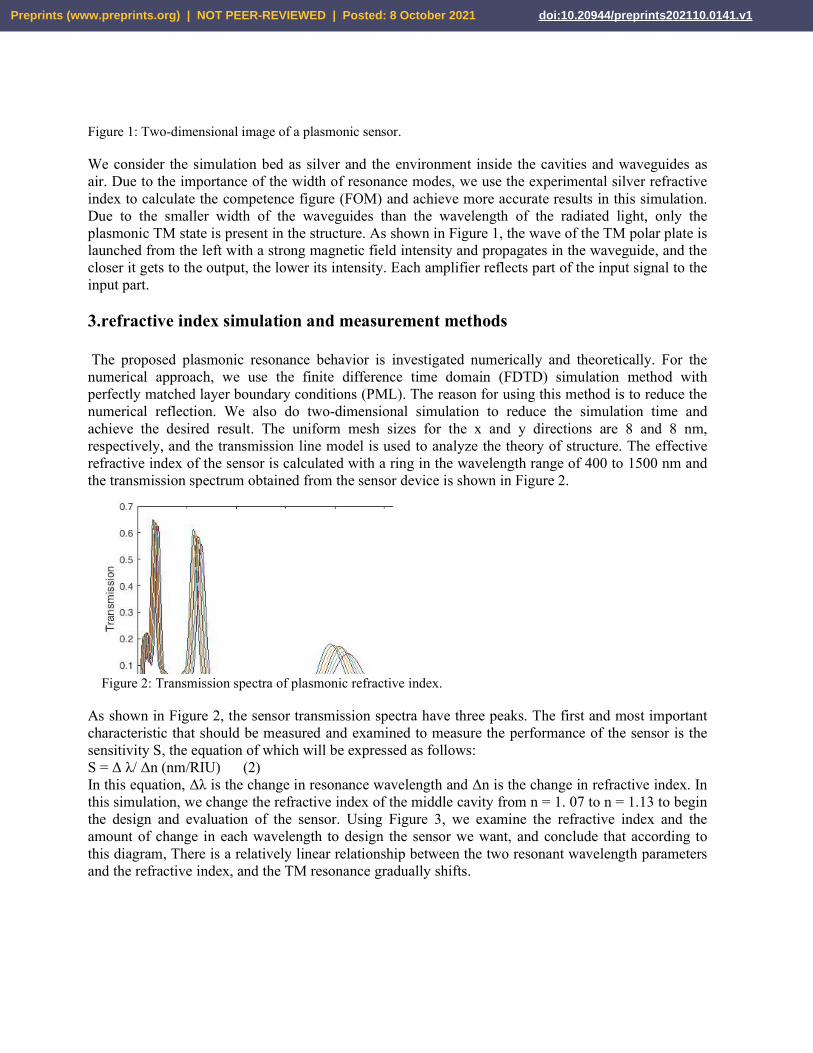
Figure 1: Two-dimensional image of a plasmonic sensor. We consider the simulation bed as silver and the environment inside the cavities and waveguides as air. Due to the importance of the width of resonance modes, we use the experimental silver refractive index to calculate the competence figure (FOM) and achieve more accurate results in this simulation. Due to the smaller width of the waveguides than the wavelength of the radiated light, only the plasmonic TM state is present in the structure. As shown in Figure 1, the wave of the TM polar plate is launched from the left with a strong magnetic field intensity and propagates in the waveguide, and the closer it gets to the output, the lower its intensity. Each amplifier reflects part of the input signal to the input part. 3.refractive index simulation and measurement methods The proposed plasmonic resonance behavior is investigated numerically and theoretically. For the numerical approach, we use the finite difference time domain (FDTD) simulation method with perfectly matched layer boundary conditions (PML). The reason for using this method is to reduce the numerical reflection. We also do two-dimensional simulation to reduce the simulation time and achieve the desired result. The uniform mesh sizes for the x and y directions are 8 and 8 nm, respectively, and the transmission line model is used to analyze the theory of structure. The effective refractive index of the sensor is calculated with a ring in the wavelength range of 400 to 1500 nm and the transmission spectrum obtained from the sensor device is shown in Figure 2.
Figure 2: Transmission spectra of plasmonic refractive index. As shown in Figure 2, the sensor transmission spectra have three peaks. The first and most important characteristic that should be measured and examined to measure the performance of the sensor is the sensitivity S, the equation of which will be expressed as follows: S = Δ λ/ Δn (nm/RIU) (2) In this equation, Δλ is the change in resonance wavelength and Δn is the change in refractive index. In this simulation, we change the refractive index of the middle cavity from n = 1. 07 to n = 1.13 to begin the design and evaluation of the sensor. Using Figure 3, we examine the refractive index and the amount of change in each wavelength to design the sensor we want, and conclude that according to this diagram, There is a relatively linear relationship between the two resonant wavelength parameters and the refractive index, and the TM resonance gradually shifts.
Preprints (www.preprints.org) | NOT PEER-REVIEWED | Posted: 8 October 2021 doi:10.20944/preprints202110.0141.v1
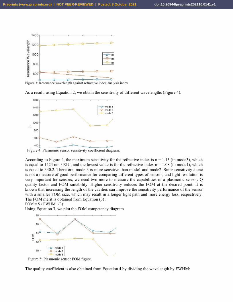
Figure 3: Resonance wavelength against refractive index analysis index As a result, using Equation 2, we obtain the sensitivity of different wavelengths (Figure 4).
Figure 4: Plasmonic sensor sensitivity coefficient diagram. According to Figure 4, the maximum sensitivity for the refractive index is n = 1.13 (in mode3), which is equal to 1424 nm / RIU, and the lowest value is for the refractive index n = 1.08 (in mode1), which is equal to 330.2. Therefore, mode 3 is more sensitive than mode1 and mode2. Since sensitivity alone is not a measure of good performance for comparing different types of sensors, and light resolution is very important for sensors, we need two more to measure the capabilities of a plasmonic sensor: Q quality factor and FOM suitability. Higher sensitivity reduces the FOM at the desired point. It is known that increasing the length of the cavities can improve the sensitivity performance of the sensor with a smaller FOM size, which may result in a longer light path and more energy loss, respectively. The FOM merit is obtained from Equation (3) : FOM = S / FWHM (3) Using Equation 3, we plot the FOM competency diagram.
Figure 5: Plasmonic sensor FOM figure. The quality coefficient is also obtained from Equation 4 by dividing the wavelength by FWHM:
Preprints (www.preprints.org) | NOT PEER-REVIEWED | Posted: 8 October 2021 doi:10.20944/preprints202110.0141.v1

/ FWHM (4) resQ = λ We see the quality coefficient diagram in Figure 6, whose value in the refractive index n = 1.13, which has the highest sensitivity coefficient, reaches 10.416.
Figure 6: Quality factor diagram of Q plasmonic sensor . Now we add to the sensor structure a ring with inner radius r2 = 80 nm and outer radius R2 = 120 nm and a cavity with length L1 = 92 nm and height W2 = 200 nm (Figure 7). The added rim and cavity are located at the bottom of the right waveguide. Figure 7: Two-dimensional image of a plasmonic sensor with two waveguides, two rings and a cavity. To measure the sensor and calculate the sensitivity, the figure of merit (FOM) and the Q quality factor in the new structure, we only change the refractive index of the middle ring and the refractive index of the waveguides and the cavity and the lower ring remain the same. Then we calculate the effective refractive index change of the sensor in the wavelength range of 400 to 1500 nm and obtain the resulting transmission spectrum (Figure 8).
SPP
inP outP
1W
Ag Air
1R
1r
2R
2r 2W
1L
Preprints (www.preprints.org) | NOT PEER-REVIEWED | Posted: 8 October 2021 doi:10.20944/preprints202110.0141.v1

Figure 8: Plasmonic refractive index sensor transmission spectra with two waveguides, two rings and a cavity . Again, we plot the refractive index changes in the selected wavelength range for the new structure, and draw a graph for the relationship between the two resonant wavelength parameters and the refractive index (Figure 9).
Figure 9: Resonance wavelength versus refractive index analysis index for plasmonic sensor with two waveguides, two rings and a cavity. We now need to obtain the sensitivity of the different wavelengths using Equation 2. According to Figure 10, the highest sensitivity is for the refractive index n = 1.09 (in mode3) which is equal to 2673 nm / RIU and the lowest value is for the refractive index n = 1.08 (in mode1) which is equal to 199 nm / RIU.
Figure 10: Plasmonic sensor sensitivity coefficient diagram with two waveguides, two rings and a cavity. We now calculate the figure of merit (FOM) and plot it (Figure 11). The value of figure of merit (FOM) in the refractive index n = 1.09, which has the highest sensitivity coefficient, reaches 17.049.
Preprints (www.preprints.org) | NOT PEER-REVIEWED | Posted: 8 October 2021 doi:10.20944/preprints202110.0141.v1

Figure 11: Plasmonic sensor figure of merit (FOM) diagram with two waveguides, two rings and a cavity. The quality factor Q diagram of this sensor is obtained using Equation 4 (Figure 12). The value of quality factor Q in the refractive index n = 1.09, which has the highest sensitivity coefficient, reaches 7.781.
Figure 12: Quality factor diagram of Q plasmonic sensor with two waveguides, two rings and a cavity. Now we add a rock with length L2 = 92 nm and height W3 = 200 nm to the left of the structure (Figure 13). Naturally, the structure of the sensor faces a new challenge, so we re-evaluate the numerical factors of the sensor. Figure 13: Two-dimensional image of a plasmonic sensor with two waveguides, two rings and a cavity. As before, to check the sensor measurement, we only change the refractive index of the middle ring in the wavelength range of 400 to 1500 nm, and the refractive index of the waveguides and cavities and the lower ring remain the same. Therefore, by calculating the change in the effective refractive index of the sensor, we obtain the resulting transmission spectrum (Figure 14).
SPP
inP outP
1W
Ag Air
1R
1r
2R
2r 2W
1L
3W
2L
Preprints (www.preprints.org) | NOT PEER-REVIEWED | Posted: 8 October 2021 doi:10.20944/preprints202110.0141.v1

Figure 14: Plasmonic refractive index sensor transmission spectra with two waveguides, two rings and two cavities. We now examine the graph of the rate of change of the refractive index in the selected wavelength range for the new structure to obtain a graph of the relationship between the resonant wavelength and the refractive index. (Figure 15).
Figure 15: Resonance wavelength against refractive index analysis index for plasmonic sensor with two waveguides, two rings and two cavities. The first criterion for measuring the performance of a sensor is its sensitivity. Therefore, we obtain the sensitivity of different wavelengths using Equation 2. According to Figure 16, the highest sensitivity is for the refractive index n = 1.09 (in mode3) which is equal to 2713 nm / RIU and the lowest value is for the refractive index n = 1.08 (in mode1) which is equal to 199.9 nm.
Preprints (www.preprints.org) | NOT PEER-REVIEWED | Posted: 8 October 2021 doi:10.20944/preprints202110.0141.v1

Figure 16: Plasmonic sensor sensitivity coefficient diagram with two waveguides, two rings and two cavities. We now calculate the FOM eligibility figure and plot it (Figure 17). The value of FOM competency digit in refractive index n = 1.09, which has the highest sensitivity coefficient, reaches 18.669.
Figure 17: Flasm diagram of the FOM diagram of a plasmonic sensor with two waveguides, two rings and two cavities. The last criterion for measuring this sensor is the quality factor Q, the diagram of which is obtained using Equation 4 (Figure 18). The value of quality coefficient Q in the refractive index n = 1.09, which has the highest sensitivity coefficient, reaches 8. 458.
Figure 18: Quality coefficient diagram of Q plasmonic sensor with two waveguides, two rings and two cavities. As shown in Table 1, the proposed method offers better results compared to some similar articles. According to this table, the maximum value of S sensitivity coefficient among these papers belongs to the structure studied in this paper, which is equal to 2713 nm.
Preprints (www.preprints.org) | NOT PEER-REVIEWED | Posted: 8 October 2021 doi:10.20944/preprints202110.0141.v1

Table 1: Comparison between
proposed sensor specifications and similar articles
conclusion
S (nm/RIU)
FOM (RIU−1)
Resonance wavelength (nm)
Topology
ReferenceS
1132 31.4 1550 Loop shaped stub
Bahramipanah et al. (2014)
868 43.9 887 Ring resonator
Yan et al. (2015)
1060 176.7 1000 Toothshaped stubs
Zafar and Salim(2015)
985 28.2 1050 Sidecoupled Waveguide
resonator
Chen and Yao(2016)
596 7.5 620 Double rectangular
cavities
Zhang et al. (2016)
860 31.6 826 Coupled double
rectangular cavities
Akhavan et al. (2017)
1125 75 1010 Rectangular and ring
resonators
Tang et al. (2017)
560 178 571 Sidecoupled Hexagon resonators
Wu et al. (2018)
806 66 826 Double sidecoupled square ring resonators
Akhavan et al. (2018)
203.8 1060 The near infrared region
Concentric double Rings
resonator
Zhang et al. (2018)
625 8.68 682 T shaped resonator
Wang et al. (2018)
1217 24.3 980 Square type split-ring resonator
Rafiee et al. (2019)
636 211.3 808 Si ring resonator
Danaie and Shahzadi. (2019)
640.6 for six resonat ors
287.9 650 Cascaded coupled
concentric ring and disk
resonator
M.Danaie et al. 2020) (
2713 18.669
1229.14 Two plasmonic
waveguides, two ring and two cavities
This work
Preprints (www.preprints.org) | NOT PEER-REVIEWED | Posted: 8 October 2021 doi:10.20944/preprints202110.0141.v1

The plasmonic sensor is a broad topic, and we highlighted the latest developments in refractive index sensors based on metal-insulated Plamonic waveguides. The structure of the sensor is analyzed numerically and theoretically. Theoretical and numerical results are obtained using the transmission line model and the time difference finite difference method, respectively. Theoretical results are consistent with numerical results. In several plasmonic resonance schemes discussed, we achieve an excellent sensitivity of 2713 nm / RIU depending on the stimulated states of the SPP. The proposed device can be used in plasmonic sensing systems in the near-infrared region. References 1-Cen C, Lin H, Huang J, Liang C, Chen X, Tang Y, Yi Z, Ye X, Liu J, Yi Y, Xiao S. (2018). A Tunable Plasmonic Refractive Index Sensor with Nanoring-Strip Graphene Arrays. Sensors. 2-Cheng F, Yang X, Gao J. (2014). Enhancing intensity and refractive index sensing capability with infrared plasmonic perfect absorbers. Opt Lett. 3-Cheng L, Wang Z, He X, Cao P. (2019). Plasmonic nanosensor based on multiple independently tunable Fano resonances. Beilstein J Nanotechnol. 4-Chou Chao CT, Chou Chau YF, Huang HJ, Kumara NTRN, Kooh MRR, Lim CM, Chiang HP. (2020). Highly Sensitive and Tunable Plasmonic Sensor Based on a Nanoring Resonator with Silver Nanorods. Nanomaterials (Basel). 5-Di Wu, Jinping Tian, Lu Li, Rongcao Yang. (2018). Plasmon induced transparency and refractive index sensing in a new type of graphene-based plasmonic waveguide. Optics Communications. 6-Wang, X.; Wu, X.; Zhu, J.; Pang, Z.; Yang, H.; Qi, Y. (2019). Theoretical Investigation of a Highly Sensitive Refractive-Index Sensor Based on TM0 Waveguide Mode Resonance Excited in an Asymmetric Metal-Cladding Dielectric Waveguide Structure. Sensors. 7-El Shamy RS, Khalil D, Swillam MA. (2020). Mid Infrared Optical Gas Sensor Using Plasmonic Mach-Zehnder Interferometer. Sci Rep. 8-Esfahani Monfared,Y. (2020). Overview of Recent Advances in the Design of Plasmonic Fiber-Optic Biosensors. Biosensors. 9-Gryga, M.; Ciprian, D.; Hlubina, P. (2020). Bloch Surface Wave Resonance Based Sensors as an Alternative to Surface Plasmon Resonance Sensors. Sensors. 10-Gomez-Cardona, N.; Reyes-Vera, E.; Torres, P. (2020). High Sensitivity Refractive Index Sensor Based on the Excitation of Long-Range Surface Plasmon Polaritons in H-Shaped Optical Fiber. Sensors. 11-Yang X, Hua E, Su H, Guo J, Yan S. (2020). A Nanostructure with Defect Based on Fano Resonance for Application on Refractive-Index and Temperature Sensing. Sensors (Basel). 12-Yangyang Chen, Jinchuan Liu, Zhenchuan Yang, James S. Wilkinson, Xiaohong Zhou. (2019). Optical biosensors based on refractometric sensing schemes: A review, Biosensors and Bioelectronics.
Preprints (www.preprints.org) | NOT PEER-REVIEWED | Posted: 8 October 2021 doi:10.20944/preprints202110.0141.v1