Plasmonic–perovskite solar cells, light emitters, and sensors
28
Ai et al. Microsystems & Nanoengineering (2022)8:5 Microsystems & Nanoengineering https://doi.org/10.1038/s41378-021-00334-2 www.nature.com/micronano REVIEW ARTICLE Open Access Plasmonic – perovskite solar cells, light emitters, and sensors Bin Ai 1,2,3 , Ziwei Fan 1 and Zi Jing Wong 1,4 ✉ Abstract The field of plasmonics explores the interaction between light and metallic micro/nanostructures and films. The collective oscillation of free electrons on metallic surfaces enables subwavelength optical confinement and enhanced light–matter interactions. In optoelectronics, perovskite materials are particularly attractive due to their excellent absorption, emission, and carrier transport properties, which lead to the improved performance of solar cells, light- emitting diodes (LEDs), lasers, photodetectors, and sensors. When perovskite materials are coupled with plasmonic structures, the device performance significantly improves owing to strong near-field and far-field optical enhancements, as well as the plasmoelectric effect. Here, we review recent theoretical and experimental works on plasmonic perovskite solar cells, light emitters, and sensors. The underlying physical mechanisms, design routes, device performances, and optimization strategies are summarized. This review also lays out challenges and future directions for the plasmonic perovskite research field toward next-generation optoelectronic technologies. Introduction Halide perovskite materials have an ABX 3 chemical formula where A can be an organic or an inorganic cation (e.g., methylammonium (MA, CH 3 NH 3 + ), for- mamidinium (FA, CH(NH 2 ) 2 + ), Cs + , Rb + , or their mix- tures), B is a divalent cation (e.g., Pb 2+ or Sn 2+ ) and X is a halide anion (e.g., I - , Br - , Cl - or their combinations). The lattice arrangement of perovskite is shown in Fig. 1a, where the larger atom A sits at the center of a cube, B occupies the corners of the cube, and the smaller atom X is on the faces of the cube. Halide perovskites have low recombination losses, large bandgap tunability, large absorption coefficients, high defect tolerance, and long charge carrier diffusion lengths and lifetimes 1–3 , all of which lead to efficient absorption, photocarrier extrac- tion, and light emission properties, as shown in Fig. 1b, c. Moreover, halide perovskites can be solution processed at low temperatures, which significantly reduces their fab- rication cost and complexity 4 . These advantages have led to the emergence of a variety of novel perovskite-based devices in the past decade 5,6 , such as solar cells (SCs) 7–10 , light-emitting diodes (LEDs) 11–14 , lasers 15–17 , photo- detectors (PDs) 18–20 , sensors 21,22 , catalyst electrodes 23–25 , field-effect transistors 26,27 , fuel cells 28,29 , memory 30,31 and spintronic devices 32,33 . However, halide perovskites are prone to phase changes and compositional degradation in the ambient environment. Despite that, the merits and prospects of halide perovskites are still very promising, and there are many passivation, encapsulation, composi- tional engineering, and novel deposition techniques to enhance halide perovskite stability. The most prominent application of halide perovskites is as light-absorbing materials in solar cells. Miyasaka and coworkers first applied halide perovskite materials in dye- sensitized solar cells in 2009 34 . In 2012, Nam Gyu Park’s group revealed the great potential of perovskites by reporting a lead iodide perovskite solar cell (PSC) with a power conversion efficiency (PCE) above 9% 35 . Since then, PSCs have experienced rapid and continuous breakthroughs in regard to their PCEs. The larger © The Author(s) 2022 Open Access This article is licensed under a Creative Commons Attribution 4.0 International License, which permits use, sharing, adaptation, distribution and reproduction in any medium or format, as long as you give appropriate credit to the original author(s) and the source, provide a link to the Creative Commons license, and indicate if changes were made. The images or other third party material in this article are included in the article’ s Creative Commons license, unless indicated otherwise in a credit line to the material. If material is not included in the article’s Creative Commons license and your intended use is not permitted by statutory regulation or exceeds the permitted use, you will need to obtain permission directly from the copyright holder. To view a copy of this license, visit http://creativecommons.org/licenses/by/4.0/. Correspondence: Zi Jing Wong ([email protected]) 1 Department of Aerospace Engineering, Texas A&M University, College Station, TX 77843, USA 2 School of Microelectronics and Communication Engineering, Chongqing University, 400044 Chongqing, P.R. China Full list of author information is available at the end of the article 1234567890():,; 1234567890():,; 1234567890():,; 1234567890():,;
-
Upload
khangminh22 -
Category
Documents
-
view
1 -
download
0
Transcript of Plasmonic–perovskite solar cells, light emitters, and sensors

Ai et al. Microsystems & Nanoengineering (2022) 8:5 Microsystems & Nanoengineeringhttps://doi.org/10.1038/s41378-021-00334-2 www.nature.com/micronano
REV I EW ART ICLE Open Ac ce s s
Plasmonic–perovskite solar cells, light emitters, andsensorsBin Ai 1,2,3, Ziwei Fan1 and Zi Jing Wong1,4✉
AbstractThe field of plasmonics explores the interaction between light and metallic micro/nanostructures and films. Thecollective oscillation of free electrons on metallic surfaces enables subwavelength optical confinement and enhancedlight–matter interactions. In optoelectronics, perovskite materials are particularly attractive due to their excellentabsorption, emission, and carrier transport properties, which lead to the improved performance of solar cells, light-emitting diodes (LEDs), lasers, photodetectors, and sensors. When perovskite materials are coupled with plasmonicstructures, the device performance significantly improves owing to strong near-field and far-field opticalenhancements, as well as the plasmoelectric effect. Here, we review recent theoretical and experimental works onplasmonic perovskite solar cells, light emitters, and sensors. The underlying physical mechanisms, design routes, deviceperformances, and optimization strategies are summarized. This review also lays out challenges and future directionsfor the plasmonic perovskite research field toward next-generation optoelectronic technologies.
IntroductionHalide perovskite materials have an ABX3 chemical
formula where A can be an organic or an inorganic cation(e.g., methylammonium (MA, CH3NH3
+), for-mamidinium (FA, CH(NH2)2
+), Cs+, Rb+, or their mix-tures), B is a divalent cation (e.g., Pb2+ or Sn2+) and X is ahalide anion (e.g., I−, Br−, Cl− or their combinations). Thelattice arrangement of perovskite is shown in Fig. 1a,where the larger atom A sits at the center of a cube, Boccupies the corners of the cube, and the smaller atom Xis on the faces of the cube. Halide perovskites have lowrecombination losses, large bandgap tunability, largeabsorption coefficients, high defect tolerance, and longcharge carrier diffusion lengths and lifetimes1–3, all ofwhich lead to efficient absorption, photocarrier extrac-tion, and light emission properties, as shown in Fig. 1b, c.Moreover, halide perovskites can be solution processed at
low temperatures, which significantly reduces their fab-rication cost and complexity4. These advantages have ledto the emergence of a variety of novel perovskite-baseddevices in the past decade5,6, such as solar cells (SCs)7–10,light-emitting diodes (LEDs)11–14, lasers15–17, photo-detectors (PDs)18–20, sensors21,22, catalyst electrodes23–25,field-effect transistors26,27, fuel cells28,29, memory30,31 andspintronic devices32,33. However, halide perovskites areprone to phase changes and compositional degradation inthe ambient environment. Despite that, the merits andprospects of halide perovskites are still very promising,and there are many passivation, encapsulation, composi-tional engineering, and novel deposition techniques toenhance halide perovskite stability.The most prominent application of halide perovskites is
as light-absorbing materials in solar cells. Miyasaka andcoworkers first applied halide perovskite materials in dye-sensitized solar cells in 200934. In 2012, Nam Gyu Park’sgroup revealed the great potential of perovskites byreporting a lead iodide perovskite solar cell (PSC) with apower conversion efficiency (PCE) above 9%35. Sincethen, PSCs have experienced rapid and continuousbreakthroughs in regard to their PCEs. The larger
© The Author(s) 2022OpenAccessThis article is licensedunder aCreativeCommonsAttribution 4.0 International License,whichpermits use, sharing, adaptation, distribution and reproductionin any medium or format, as long as you give appropriate credit to the original author(s) and the source, provide a link to the Creative Commons license, and indicate if
changesweremade. The images or other third partymaterial in this article are included in the article’s Creative Commons license, unless indicated otherwise in a credit line to thematerial. Ifmaterial is not included in the article’s Creative Commons license and your intended use is not permitted by statutory regulation or exceeds the permitted use, you will need to obtainpermission directly from the copyright holder. To view a copy of this license, visit http://creativecommons.org/licenses/by/4.0/.
Correspondence: Zi Jing Wong ([email protected])1Department of Aerospace Engineering, Texas A&M University, College Station,TX 77843, USA2School of Microelectronics and Communication Engineering, ChongqingUniversity, 400044 Chongqing, P.R. ChinaFull list of author information is available at the end of the article
1234
5678
90():,;
1234
5678
90():,;
1234567890():,;
1234
5678
90():,;

bandgaps of halide perovskites compared with traditionalphotovoltaic materials such as Si and GaAs also enablethem to form tandem solar cells with lower-bandgapphotovoltaic materials to attain even higher PCEs. Fur-thermore, PSCs offer additional attributes such as theirsemitransparency, light weight, and flexibility. The PCEsof PSCs have now exceeded 25%, which is only slightlylower than the 27.6% PCE of the best single-crystallinesilicon solar cells36. In addition to improving materialquality and stability of perovskites, new design strategiesto further improve the PCE are critical for next-generation photovoltaics (PVs).Halide perovskites have also been used as light-emitting
materials in LEDs and lasers. In perovskites, holes andelectrons are confined into inorganic [PbX6]
4− octahedralnetworks, leading to strong Coulomb interactions andexcitonic effects. They also have the advantages of a highquantum yield (QY), narrow band emission, and widecolor tunability across the entire visible and infraredregion, which makes them a promising material to use inlight-emitting devices. CsPbBr3 perovskite nanocrystals(NCs) exhibit a high photoluminescence quantum yield(PLQY) of ~97%37. Moreover, the emission color can befacilely tuned in the visible range (blue to red) by varying
the halide anion (Cl−, Br−, or I−), showing the potential ofperovskites in white LEDs38,39. Recently, the efficiency ofLEDs reached 108 cd/A (external quantum efficiency(EQE) of 23.4%) and was further increased to 205 cd/A(EQE of 45.5%) with a hemispherical lens40. Comparedwith those of mature technologies such as organic LEDs(EQE of 25%)41 and inorganic quantum dot LEDs (20.5%),this is a high efficiency42. Similarly, low-threshold laserscan also be achieved using halide perovskites as the gainmaterials. The optical gain coefficients of lead-halideperovskites can be comparable to those of conventionalbulk semiconductors, such as GaAs43. Moreover, theemission wavelengths of lead-halide perovskite lasers canbe tuned from ultraviolet to near-infrared (NIR) by con-trolling the composition44–46, filling the green emissiongap between III-nitrides and III-phosphides. Variousperovskite microlasers have been realized by micro-plates47, micro/nanorods48, microdisks49, and photoniccrystals50,51. Recently, continuous wave (CW)-pumpedMAPbX3 perovskites have been reported, showing thepossibility of electrically driven perovskite microlasers52.Perovskite lasers can also realize unidirectional emis-sions49, mode control53, and high-density laser arrays54,55.Despite rapid progress, there is considerable room to
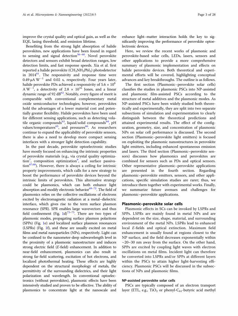
A (MA+, FA+, Cs+ , etc.)
1.0
a b
0.5
Pho
tolu
min
esce
nce
(nor
m.)
0.0500 600
Plasmon polaritons�2 = (kc)2 + �2
�p
�sp
Dielectric light line� = ck0
Freq
uenc
y �
Surface plasmon polaritons
Wavevector kx
11/2+
=
700 800
Wavelength (nm)
900
B (Pb2+, Sn2+, Ge2+ , etc.)
C (CI–, Br –, I– , etc.)
p
�ckx
�1 �2
�1�2
Gold sphere
Electric field
+++
+++– – –
Electron cloud
Time
– – –
+++– – – – – –+++– – –
c
d e f
100
10–1
Abs
orba
nce
(nor
m.)
10–2
10–3
10–4
a
Fig. 1 Outline of perovskites and plasmonics. a Structure of a halide perovskite unit cell. b Photoluminescence spectrum (left axis) and absorptionspectrum as measured by photothermal deflection spectroscopy (PDS, right axis) of a (Cs0.06MA0.15FA0.79)Pb(I0.85Br0.15)3 thin film. Adapted withpermission213. Copyright 2019, Wiley. c Schematic of the process of photocarrier extraction and light emission. d Photon dispersion in the bulk of ametal and surface plasmon polariton dispersion on the surface of the same metal and a dielectric. e Surface plasmon polariton (SPP) and (f) localizedsurface plasmon resonance modes (LSPRs).
Ai et al. Microsystems & Nanoengineering (2022) 8:5 Page 2 of 28
improve the crystal quality and optical gain, as well as theEQE, lasing threshold, and emission lifetime.Benefiting from the strong light absorption of halide
perovskites, new applications have been found in regardto sensing and signal detection56–60. Novel perovskitedetectors and sensors exhibit broad detection ranges, lowdetection limits, and fast response speeds. Xia et al. firstreported a halide perovskite (CH3NH3PbI3) photodetectorin 201461. The responsivity and response time were0.49 μAW−1 and 0.02 s, respectively. Four years later,halide perovskite PDs achieved a responsivity of 5.6 × 10⁸
AW−1, a detectivity of 2.8 × 10¹⁶ Jones, and a lineardynamic range of 92 dB62. Notably, every figure of merit iscomparable with conventional complementary metaloxide semiconductor technologies; however, perovskiteshold the advantages of a lower material cost and poten-tially greater flexibility. Halide perovskites have been usedfor different sensing applications, such as detecting vola-tile organic compounds63, liquid/solid compounds64, pHvalues/temperatures65, and pressures66. As researcherscontinue to expand the applicability of perovskite sensors,there is also a need to develop more compact sensinginterfaces with a stronger light detection capability.In the past decade, perovskite optoelectronic studies
have mostly focused on enhancing the intrinsic propertiesof perovskite materials (e.g., via crystal quality optimiza-tion7, composition optimization9, and surface passiva-tion67,68). However, there is always a ceiling for intrinsicproperty improvements, which calls for a new strategy toboost the performance of perovskite devices beyond theintrinsic limits of perovskites. This alternative strategycould be plasmonics, which can both enhance lightabsorption and modify electronic behavior69–72. The field ofplasmonics relies on the collective oscillations of electronsexcited by electromagnetic radiation at a metal–dielectricinterface, which gives rise to the term surface plasmonresonance (SPR). SPR enables large wavevectors and thusfield confinement (Fig. 1d)73–75. There are two types ofplasmonic modes, propagating surface plasmon polaritons(SPPs) (Fig. 1e) and localized surface plasmon resonances(LSPRs) (Fig. 1f), and these are usually excited on metalfilms and metal nanoparticles (NPs), respectively. Light canbe confined to the nanometer-deep subwavelength level inthe proximity of a plasmonic nanostructure and inducesstrong electric field (E-field) enhancement. In addition tonear-field enhancement, plasmonics can also result instrong far-field scattering, excitation of hot electrons, andlocalized photothermal heating. These effects are highlydependent on the structural morphology of metals, thepermittivity of the surrounding dielectrics, and their lightpolarization and wavelength. In conventional optoelec-tronics (without perovskites), plasmonic effects have beenintensively studied and proven to be effective. The ability ofplasmonics to concentrate light at the nanoscale and
enhance light–matter interaction holds the key to sig-nificantly improving the performance of perovskite optoe-lectronic devices.Here, we review the recent works of plasmonic and
perovskite-based solar cells, LEDs, lasers, sensors andother applications to provide a more comprehensivesummary of plasmonic implementation and effects onhalide perovskite devices. Both theoretical and experi-mental efforts will be covered, highlighting conceptualadvances and key breakthroughs. The outline is as follows.The first section (Plasmonic–perovskite solar cells)
classifies the studies in plasmonic PSCs into NP-assistedand plasmonic film-assisted PSCs according to thestructure of metal additives and the plasmonic modes. AsNP-assisted PSCs have been widely studied both theore-tically and experimentally, they are split into two separatesubsections of simulation and experimentation to clearlydistinguish between the theoretical predictions andattained experimental results. The effect of the config-uration, geometry, size, and concentration of plasmonicNPs on solar cell performance is discussed. The secondsection (Plasmonic–perovskite light emitters) is focusedon exploiting the plasmonic nanostructures in perovskitelight emitters, including enhanced spontaneous emissionand lasers. The third section (Plasmonic–perovskite sen-sors) discusses how plasmonics and perovskites arecombined for sensors such as PDs and optical sensors.Other representative plasmonic–perovskite applicationsare presented in the fourth section. Regardingplasmonic–perovskite emitters, sensors, and other appli-cations, specific simulation studies are rarer; thus, weintroduce them together with experimental works. Finally,we summarize future avenues and challenges forplasmonic–perovskite applications.
Plasmonic–perovskite solar cellsPlasmonic effects in SCs can be invoked by LSPRs and
SPPs. LSPRs are mainly found in metal NPs and aredependent on the size, shape, material, and surroundingenvironment of the metal NPs. LSPRs lead to enhancedlocal E-fields and optical extinction. Maximum fieldenhancement is usually found at regions closest to theNP surface, and the field decreases exponentially within~20–30 nm away from the surface. On the other hand,SPPs are excited by coupling light waves with electronoscillations on metal films. Incident light can thereforebe converted into LSPRs and/or SPPs at different layerswithin the PSCs to attain higher light-harvesting effi-ciency. Plasmonic PSCs will be discussed in the subsec-tions of NPs and plasmonic films.
NP-assisted perovskite solar cellsPSCs are typically composed of an electron transport
layer (ETL, e.g., TiO2 or phenyl-C61-butyric acid methyl
Ai et al. Microsystems & Nanoengineering (2022) 8:5 Page 3 of 28

ester (PCBM)), an active layer (halide perovskite), and ahole transport layer (HTL, e.g., poly(3,4-ethylenediox-ythiophene)-poly(styrenesulfonate) (PEDOT:PSS) orspiro-OMeTAD) sandwiched by a transparent electrode(fluorine-doped tin oxide (FTO) or indium-doped tinoxide (ITO)) and a metal electrode (Au, Ag, or Al). Inprinciple, NPs can be incorporated in ETLs, perovskitelayers, and HTLs to alter light absorption. It is imperativeto systematically summarize PV performances and clarifythe underlying enhancement mechanisms and effects ofthe NP geometry, size, concentration, position, andcomposition. In the following, we first introduce theadvances in simulation and then the experimental results.
Simulations of NP-assisted perovskite solar cellsSpherical NPs are used most commonly in PSCs and are
usually studied by embedding them in the perovskitelayer; one example is shown in Fig. 2a76,77. Chang et al.assessed the optical effects of Cu NPs embedded in aperovskite film by the transfer matrix method (TMM)and three-dimensional finite difference time domain (3DFDTD) method78. The thickness of the perovskite andthe gap size between Cu NPs were varied, which led to theconclusions that Cu NPs could reduce the perovskitethickness from 400 nm to 300 nm while maintainingthe absorption strength and that the absorbance at λ =350–760 nm increased by 1.7% when the gap size was30 nm (NP diameter was 70 nm). The trapping of incident
light between the Cu NPs and perovskite led to a higherabsorption efficiency. Palacios et al. presented an FDTD-based PSC model with Au NPs to analyze the effect ofsize, concentration, and location in the perovskite film79.Solar absorption could be enhanced by ∼10% when thethickness of the perovskite films was 200 nm and theradius of the spheres was 60 nm. The enhancementwas ∼6% when the thickness of the perovskite films was300 nm and the radius of the spheres was 90 nm. Theenhanced absorption results arose from both the plas-monic near-field and scattering effects. Pathak et al. cal-culated the optical cross-section of arbitrarily sized andspherical-shaped metal NPs with perovskite by Mie scat-tering theory80. They found that NPs with a radius of15 nm and volume concentration of approximately 10%achieved the highest scattering efficiency. The absorptionand scattering efficiencies of Ag NPs with varying sizes,shapes, and polarizations of linearly polarized light werestudied using the discrete dipole approximation (DDA)method in the active layer of PSCs81. Researchers foundthat the incorporation of Ag NPs in the active layer ofPSCs led to a strong LSPR. Yue et al. proposed a full-wavesimulation approach to demonstrate the effects of closelyand regularly spaced Ag NPs in the perovskite layer ofPSCs82. The infrared absorption of the PSC integratedwith Ag NPs was enhanced by 58.2%. Coated anduncoated Ag NPs (radii ranging from 10 to 15 nm) werestudied to understand the plasmonic interaction with
Au
a b c d
Ag Au
Perovskite
Air
Spiro-OMeTAD
CH3NH3PbI3
Au/SiO2
Perovskite medium
AI NPs array
30 nm 30 nm
20 nm
Glass
MAPbl3
Spiro-O
MeTAD
ITO
Gold back mirror
glass FTO lumpy NPUnit Cell Unit Cell Unit Cell
perovskite perovskite perovskite
D
H
Aluminium Aluminium Aluminium
Mesh space
Au
TiO2
CH3NH3PbI3
Spiro-OMeTAD
x z
y
e f g
AI
TiO 2
LR
Fig. 2 Different configurations of simulated plasmonic nanoparticle-assisted perovskite solar cells. Schematics of plasmonic–perovskite solarcells by incorporating (a) Au nanoparticles (NPs). Adapted with permission76. Copyright 2019, MPDI. b Ag–Au dimer. Adapted with permission84.Copyright 2017, SPIE. c Two Au–SiO2 core–shell nanoparticles. Adapted with permission85. Copyright 2018, IOP Publishing, Ltd. d Al nanoparticlearray. Adapted with permission87. Copyright 2019, OSA Publishing. e Lumpy nanoparticles on the rear surface. Adapted with permission90. Copyright2015, OSA Publishing. f Spherical, cylindrical, and conic NP arrays on the rear surfaces. Adapted with permission91. Copyright 2018, Elsevier. g AgNWnanocross array. Adapted with permission93. Copyright 2017, OSA Publishing. The TMM and 3D FDTD method were used for (a). The plasmonhybridization, dipolar–dipolar coupling method, and FDTD simulation were used for (b). The 3D FDTD method was used for (c). Effective mediumtheory and a detailed balance analysis were applied for (d). FDTD was used for (e–g).
Ai et al. Microsystems & Nanoengineering (2022) 8:5 Page 4 of 28
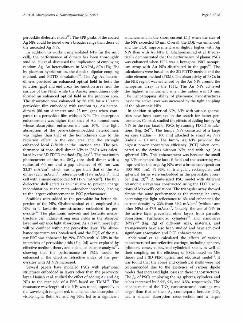
perovskite dielectric media83. The SPR peaks of the coatedAg NPs could be tuned over a broader range than those ofthe uncoated Ag NPs.In addition to works using isolated NPs (in the unit
cell), the performance of dimers has been thoroughlystudied. Hu et al. discussed the implication of employingrandom Ag–Au heterodimers in MAPbI3 SCs (Fig. 2b)by plasmon hybridization, the dipolar–dipolar couplingmethod, and FDTD simulation84. The Ag–Au hetero-dimers provided an enhanced optical field in both thejunction (gap) and end areas (no-junction area near thesurface of the NPs), while the Au/Ag homodimers onlyformed an enhanced optical field in the junction area.The absorption was enhanced by 28.15% for a 150-nmperovskite film embedded with random Ag–Au hetero-dimers (80-nm diameter and 25-nm gap) when com-pared to a perovskite film without NPs. The absorptionenhancement was higher than that of Au homodimerswhose absorption enhancement was 10%. The lightabsorption of the perovskite-embedded heterodimerswas higher than that of the homodimers due to theradiation effect in the end area and the stronglyenhanced local E-fields in the junction area. The per-formance of core–shell dimer NPs in PSCs was calcu-lated by the 3D FDTD method (Fig. 2c)85. The maximumphotocurrent of the Au–SiO2 core–shell dimer with aradius of 60 nm and a gap distance of 60 nm was23.37 mA/cm2, which was larger than that of the Audimer (22.5 mA/cm2), reference cell (19.8 mA/cm2), andcell with a single embedded NP (17.9 mA/cm2). The thindielectric shell acted as an insulator to prevent chargerecombination at the metal–absorber interface, leadingto the largest enhancement in PSC performance.Scaffolds were added to the perovskite for better dis-
persion of the NPs. Ghahremanirad et al. employed AuNPs in a kesterite mesostructure embedded in per-ovskite86. The plasmonic network and kesterite mesos-tructure can induce strong near fields in the absorberlayer and enhance light absorption. As a result, more lightwill be confined within the perovskite layer. The absor-bance spectrum was broadened, and the EQE of the pla-nar PSC was enhanced by 29%. PSCs with Al NPs in theinterstices of perovskite grids (Fig. 2d) were explored byeffective medium theory and a detailed balance analysis87,showing that the performance of PSCs would beenhanced if the effective refractive index of the per-ovskites with Al NPs increased.Several papers have modeled PSCs with plasmonic
structures embedded in layers other than the perovskitelayer. Hajjiah et al. studied the effect of adding Au and AgNPs to the rear side of a PSC based on TMM88. Theresonance wavelength of the NPs was tuned, especially inthe wavelength range of red, to enhance the absorption ofvisible light. Both Au and Ag NPs led to a significant
enhancement in the short current (Jsc) when the size ofthe NPs exceeded 40 nm. Overall, the EQE was enhanced,and the EQE improvement was slightly higher with AgNPs than with Au NPs. E. Ghahremanirad et al. theore-tically demonstrated that the performance of planar PSCswas enhanced when HTL was a hexagonal NiO nanopr-ism array with Au NPs distributed in the gaps89. Thecalculations were based on the 3D FDTD method and thefinite element method (FEM). The absorptivity of PSCs inthe NIR region was enhanced by the Au NPs around thenanoprism array in the HTL. The Au NPs achievedthe highest enhancement when the radius was 10 nm.The light-trapping ability of plasmonic nanostructuresinside the active layer was increased by the tight couplingof the plasmonic NPs.In addition to spherical NPs, NPs with various geome-
tries have been examined in the search for better per-formance. Cai et al. studied the effects of adding lumpy AgNPs to the rear facet of PSCs by running FDTD simula-tions (Fig. 2e)90. The lumpy NPs consisted of a largeAg core (radius = 100 nm) attached to small Ag NPs(radius = 10 nm). The lumpy Ag NPs provided thehighest power conversion efficiency (PCE) when com-pared to the devices without NPs and with Ag (Au)spherical NPs. This enhancement was because the smallAg NPs enhanced the local E-field and the scattering wasimproved by the large Ag NPs over a broadband spectrum(300–900 nm). Pt NPs in triangular, rectangular, andspherical forms were embedded in the perovskite absor-ber (Fig. 2f)91. A finite-sized PSC model with differentplasmonic arrays was constructed using the FDTD solu-tions of Maxwell’s equations. The triangular array showedalmost the same performance as the rectangular array,decreasing the light reflectance to 6% and enhancing thecurrent density by 22% from 39.2 mA/cm2 (without anyother NPs) to 47.9 mA/cm2. Notably, the use of NPs inthe active layer prevented other layers from parasiticabsorption. Furthermore, cylinders92 and nanowires(NWs)93 (Fig. 2g) of different sizes, materials, andarrangements have also been studied and have achievedsignificant absorption and PCE enhancements.Abdelraouf et al. calculated the effects of various
nanostructured antireflective coatings, including spheres,cylinders, cones, cubes, and cylindrical shells, as well astheir coupling, on the efficiency of PSCs based on Mietheory and a 3D FEM optical and electrical model94. Itwas found that the cones and cylindrical shells were notrecommended due to the existence of various dipolemodes that increased light losses in these nanostructures.The Jsc of PSCs employing the Ag spheres, cylinders, andcubes increased by 8.9%, 9%, and 3.5%, respectively. Theenhancement of the TiO2 nanostructured coatings waslarger than that of their Ag counterparts because TiO2
had a smaller absorption cross-section and a larger
Ai et al. Microsystems & Nanoengineering (2022) 8:5 Page 5 of 28
scattering cross-section over the solar spectrum. The Jsc ofPSCs with TiO2 spheres and cylinders increased by 12.8%and 15%, respectively. Researchers also found that themetasurface cross-grating nanostructure within PSCswould increase the photocurrent and enhance the overallefficiency95. Enhanced light absorption and reduced lightreflection are highly dependent on the dimensions, peri-odicity, and coating material of the grating nanos-tructures. TiO2 metasurfaces above and below theperovskite layer led to an increase in Jsc from 19.2 to 22.1mA/cm2, while the Au metasurfaces achieved a Jsc of21.13 mA/cm2.More recently, Perrakis et al. presented detailed and
systematic work on the implementation of metal NPs inPSCs96. CST Microwave Studio was used to perform 3Dfull-wave electromagnetic simulations. The PSC structurewas SiO2 (1.1 mm)/ITO (100 nm)/PEDOT:PSS (40 nm)/MAPbI3/PCBM (50 nm)/Al (100 nm); the thickness ofeach layer is indicated in the brackets. Metal NPs withdifferent materials, vertical positions, sizes, concentra-tions, clustering formations, and coatings were studied. Itwas demonstrated that (a) the optimum response of AgNPs was with a radius of 60–70 nm, especially when in theproximity of the top of the perovskite layer. Furthermore,the optimum NP distance was ~300 nm; (b) the effect ofNP randomness, angle of incidence, and polydispersitywas very limited on the calculated enhancement; (c) theAl nanospheres with radii of 18 nm and a gap distance of65 nm had the optimum performance; (d) the photo-current was largely enhanced (up to 4.0% correspondingto photocurrent density (Jph) = 21.22 mA/cm2) when NPswere in the HTL (PEDOT:PSS, on top of the perovskitelayer)and (e) the largest absorption enhancement wasachieved when Al and Ag spheres were both used in thePEDOT:PSS layer and perovskite layer, respectively.Devices with Ag spheres embedded in the perovskite andAl spheres inside the HTL (PEDOT:PSS) can increase thePCE to ~12%. The origin of the photocurrent enhance-ment was attributed to the strong local E-field arisingfrom the plasmonic resonances, and the larger scatteringand antireflection due to the NPs, especially when the NPswere close to the top of the perovskite layer.The above theoretical works studying the effect of
plasmonic NPs on PSCs focused on characterizing PVperformance, explaining the operational mechanism,and optimizing the NPs. Valuable primary results can beextracted from these theoretical models/simulations: (1)PV performance can be enhanced by incorporating NPs inPSCs; (2) the enhancement is due to the near-fieldabsorption and far-field scattering of NPs induced byLSPR; (3) the geometry, size, material, density, distance,position, number, and coating all play important roles inenhancing PV performance. In addition, the absorptionenhancement allows employment of PSCs with very thin
perovskite layers, e.g., 150 nm, while at the same timemaintaining the same performance as that of non-plasmonic PSCs with the optimum thickness (350 nm)96.Therefore, plasmonic NPs significantly reduce toxicityand make PSCs more environmentally friendly. Thesimulation demonstrates that embedding plasmonic NPsinto PSCs is a powerful strategy to improve photoelectricperformance. Although many simulations have beenperformed, challenges and issues still exist. The simula-tions should involve more materials and geometriesof NPs. Most of the simulations are focused on NPsembedded in perovskite, while more works studying theeffects of NPs in the ETLs, HTLs, and combined layers areneeded to provide more design possibilities. There arenonnegligible differences between the simulation modelsand realistic devices, such as deviations in the opticalconstants of the materials and the film quality in the realdevice not being as perfect as that in the simulations.Most of the simulations are focused on optical absorptionfor evaluating PV performance. Furthermore, the elec-trical properties of the metal, which lead to an increase inconductivity and electron–hole recombination, are nottaken into account. This will bring about large dis-crepancies between the simulations and real devices.Overall, the simulations provide important theoreticalguidelines, but the experimental ways of implementingNPs in PSCs still need to be explored.
Experiments of NP-assisted perovskite solar cellsGenerally, plasmonic PSC experiments are focused on
the configuration (NP position), modification of the NPs(material, geometry, size, and concentration), PV perfor-mance (PCE) enhancement, and underlying mechanism.The results are summarized in Table 1 in chronologicalorder. Statistical analysis is performed based on theseresults with the following conclusions.The position of the NPs can be in the ETLs (PCBM,
TiO2, Al2O3, and SnO2), perovskite, and HTLs (spiro-OMeTAD, PEDOT:PSS, and VOx). In simulations, per-ovskite is the major layer where the effect of NPs isstudied, whereas the experiments mainly examine theuse of plasmonic NPs in the ETLs and HTLs and at theETL/HTL–perovskite interfaces. The NPs can be wellblended into solutions of spiro-OMeTAD, PEDOT:PSS,and PCBM, which are then made into thin films as thebuilding blocks of the device by facile spin-coating. Leeet al. found that when the spiro-OMeTAD HTL solutionwith Au NPs was spin-coated, the Au NPs could natu-rally stay close to the perovskite layer77. This rule likelyalso applies to the spin-coating of PEDOT:PSS andPCBM solutions with NPs. This distributes the NPs atthe interface between the perovskite layer and spiro-OMeTAD or PBCM layer because these two materialsare typically spin-coated after the perovskite layer.
Ai et al. Microsystems & Nanoengineering (2022) 8:5 Page 6 of 28

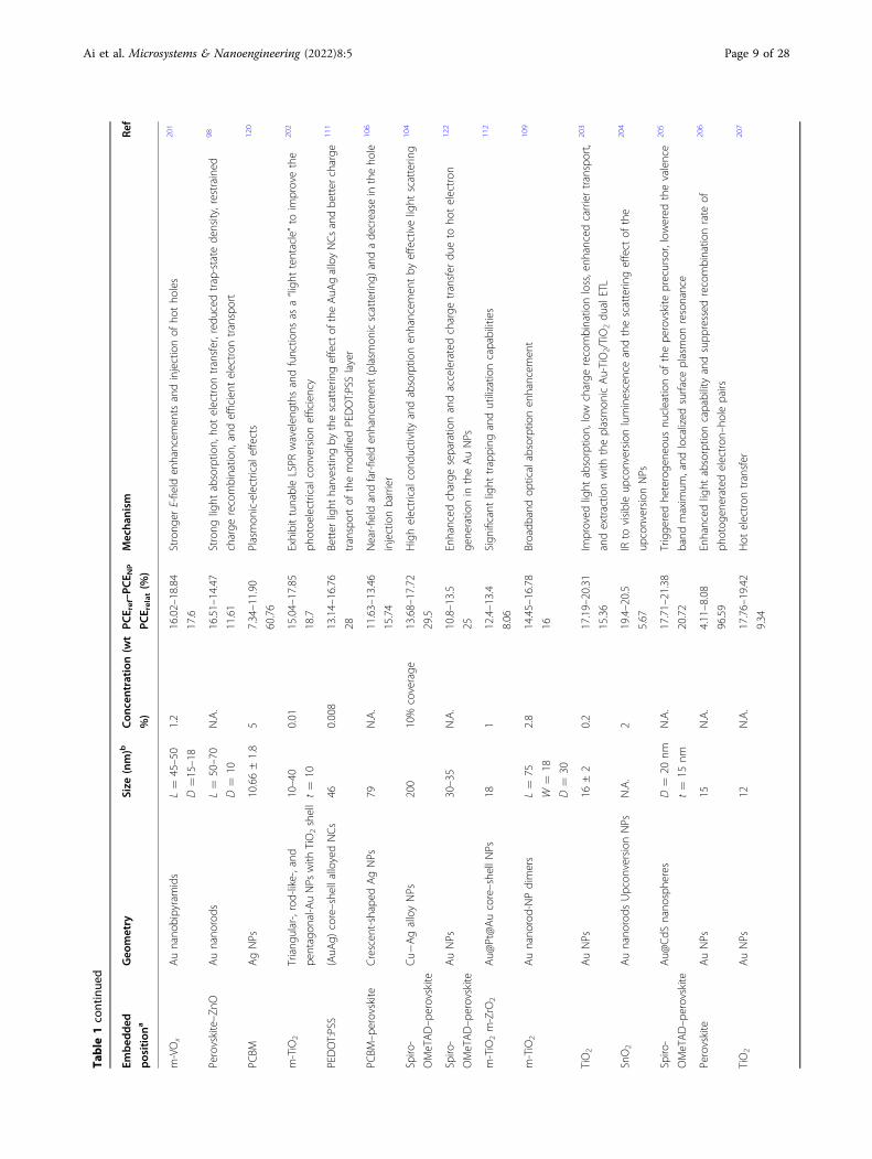
Table
1Em
bed
ded
position,NPparam
eters(geo
metry,size,an
dco
ncentration)PC
E,an
dmechan
ismsof
theex
perim
entalNP-assisted
perov
skitesolarcells
Embed
ded
positiona
Geo
metry
Size
(nm)b
Con
centration
(wt
%)
PCE r
ef–PC
E NP
PCE r
elat(%
)
Mecha
nism
Ref
m-Al 2O3
Core–shellA
u@SiO2NPs
D=
80
t=
8
0.9
8.4–9.5
13.1
Redu
cedexcitonbind
ingen
ergy
with
theincorporationof
metalNPs,rathe
rthan
enhanced
light
absorptio
n
193
PEDOT
Agnano
triang
les
700.83
8.5–9.6
12.9
Increasedplasmon
icscatterin
geffect
194
m-TiO
2Au-Agalloypo
pcorn-shaped
NPs
150±50
0.7
8.9–10.3,
15.7
Opticalabsorptio
nen
hancem
entandfaster
charge
transfer
195
m-Al 2O3
Ag@
TiO2
422.2
14.5–16.3
12.41
Ligh
treem
itted
from
theradiativerecombinatio
nof
electron
–holepairs
andph
oton
recycling
115
Spiro
-
OMeTAD–p
erovskite
AuNPs
150.01
12.66–12.74
0.63
LSPR
andtheelectricaleffect
77
m-TiO
2Au-de
coratedTiO2nano
fibe
rs58
0.3
9.23–14.92
61.64
Enhancem
entof
light
absorptio
n,bu
talso
contrib
utes
toredu
cedcharge
recombinatio
nin
Au@
TiO2nano
fibe
relectrod
es
119
m-TiO
2AgNPs
3020
4.57–6.15
34.57
Extend
stheop
ticalpathway
ofincide
ntlight
andtheelectron
transporttim
e196
m-TiO
2Au@
SiO2nano
rods
L=
39
D=
13
t=
15
412.4–14.4
13.5
Cross-sectio
nalscatteringandspectrallyabsorbed
energy
density.
114
Perovskite–PED
OT:
PSS
Au@
SiO2nano
rods
L=34.7
D=
16.8
t=
9.5
0.047pM
10.9–15.6
40
TheLSPR
oftheAu@
SiO2nano
rods
couldim
provetheincide
ntlight
trapping
aswellas
improvethetransportandcollectionof
thecharge
carrier
101
m-TiO
2AgNPs
250.5
10.96–11.96
9.1
LSPR,chargetrapping
,and
surface
roug
hness
107
m-TiO
2SiO2@
Ag@
TiO2NWs
10N.A.c
12.17–15.09
24
Plasmon
ic-enh
ancedlight
absorptio
nandincreasedrecombinatio
nresistance
197
m-TiO
2Aunano
stars
20–30
0.5
15.19–17.72
16.66
Enhanced
light
absorptio
nandsupp
ressed
charge
recombinatio
n108
c-TiO2d
Au-Agnano
alloyNPs
4020
12.64–13.91
10.04
Increasedlight
harvestin
gdu
eto
theincreasedop
ticalpath
leng
thcaused
bythelight
scatterin
gof
themetallic
nano
structures
110
m-TiO
2Au@
TiO2nano
rods
L=
32
D=
8
t=
5
115.51–16.78
8.2
Better
charge
separatio
n/transfer
aswellasfacilitated
carriertransportin
thepresen
ce
ofplasmon
icNPs
118
Ai et al. Microsystems & Nanoengineering (2022) 8:5 Page 7 of 28
Table
1continue
d
Embed
ded
positiona
Geo
metry
Size
(nm)b
Con
centration
(wt
%)
PCE r
ef–PC
E NP
PCE r
elat(%
)
Mecha
nism
Ref
m-TiO
2Au@
Agcore–she
llnano
cubo
ids
L=55
W=
11.5
l=10–25
t=
6–10.5
2.9–3.8
15.16–18.31
20.78
Both
plasmon
icne
ar-fielden
hancem
entandincreasedlight-scatteringeffects
116
Spiro
-OMeTAD
Aunano
stars
350.02
12.49–13.97
14
SPR,backscatterin
g,andcharge
transport
121
PCBM
–BCP
Agnano
cube
s70
N.A.
11.9–13.3
11.76
Far-fieldscatterin
gandop
ticalne
arfield
139
c-TiO2–FTO
AgNPs
11N.A.
7.78–7.08
22.5
Chargeseparatio
nandtrapping
ofelectron
s117
m-TiO
2and
perovskite
Au@
TiO2
80N.A.
12.59–18.24
44
Carriertransport
102
m-TiO
2Au@
SiO2core–she
llNPs
201
3.78–4.49
18
Enhanced
absorptio
n126
Perovskite–N
iOAuisland
s10
N.A.
2.2–4.8
118.18
Strong
scatterin
ganden
hancem
entof
theE-field
100
PEDOT:PSS
AgNPs
SiO2NPs
5010
11particle
mL−
113.3–14
5.3
Increasedcharge
selectivity
anden
hanced
charge
collectionprop
ertiesacross
the
interface
198
Perovskite–TiO
2Ag@
SiO2NWs
L=
5–10
μm
D=
80
0.06
14.32–18.03
25.9
Fastelectron
transm
ission
,highlight
harvestin
g,electron
–holeseparatio
n,andLSPR
97
m-TiO
2Au/Agnano
cube
scapp
edwith
a
thin
∼4nm
layerof
SiO2
~60
13.9–4.9
26
Improved
hotcarrierthermalizationto
aneq
uilibriu
mdistrib
ution,
enhanced
photoind
uced
carrierge
neratio
n,andprom
oted
efficien
telectron
injection
199
m-TiO
2AuNPs
coated
byMgO
40N.A.
12–16.1
34.2
Minim
ized
photon
icanden
ergy
losses
forthege
neratio
nof
carriers,leading
toahigh
charge
transportcapabilityandlow
charge
recombinatio
n
127
m-TiO
2Aunano
rod@
SiO2
L=
40
D=
15
t=
8
0.09
14.39–17.39
20.85
Scatterin
geffect,p
hotonabsorptio
n,andsupe
rioren
hanced
charge
separatio
n200
Perovskite–PED
OT:
PSS
Au@
SiO2core–she
llD=
40
t=
2
1.2
11.44–14.57
27.3
LSPR
,light
absorptio
n,faster
charge
transporttim
e,andlong
errecombinatio
nlifetim
e99
PCBM
–perovskite
AgNPs
with
prop
anethiol
N.A.
0.24
9.69–11.26
16.2
Scatterin
gcontrib
uted
toincreasedcharge
gene
ratio
n/transportwith
redu
ced
recombinatio
n
113
Ai et al. Microsystems & Nanoengineering (2022) 8:5 Page 8 of 28
Table
1continue
d
Embed
ded
positiona
Geo
metry
Size
(nm)b
Con
centration
(wt
%)
PCE r
ef–PC
E NP
PCE r
elat(%
)
Mecha
nism
Ref
m-VOx
Aunano
bipyramids
L=
45–50
D=15–18
1.2
16.02–18.84
17.6
Strong
erE-fielden
hancem
entsandinjectionof
hotho
les
201
Perovskite–Z
nOAunano
rods
L=
50–70
D=
10
N.A.
16.51–14.47
11.61
Strong
light
absorptio
n,ho
telectron
transfer,red
uced
trap-state
density,restraine
d
charge
recombinatio
n,andefficien
telectron
transport
98
PCBM
AgNPs
10.66±1.8
57.34–11.90
60.76
Plasmon
ic-electricaleffects
120
m-TiO
2Triang
ular-,rod-like-,and
pentagon
al-AuNPs
with
TiO2shell
10–40
t=
10
0.01
15.04–17.85
18.7
ExhibittunableLSPR
wavelen
gths
andfunctio
nsas
a“ligh
ttentacle”to
improvethe
photoe
lectricalconversion
efficien
cy
202
PEDOT:PSS
(AuA
g)core–she
llalloyedNCs
460.008
13.14–16.76
28
Better
light
harvestin
gby
thescatterin
geffect
oftheAuA
galloyNCsandbe
tter
charge
transportof
themod
ified
PEDOT:PSSlayer
111
PCBM
–perovskite
Crescen
t-shaped
AgNPs
79N.A.
11.63–13.46
15.74
Near-fieldandfar-fielden
hancem
ent(plasm
onicscatterin
g)andade
crease
intheho
le
injectionbarrier
106
Spiro
-
OMeTAD–p
erovskite
Cu−
AgalloyNPs
200
10%
coverage
13.68–17.72
29.5
Highelectricalcond
uctivity
andabsorptio
nen
hancem
entby
effectivelight
scatterin
g104
Spiro
-
OMeTAD–p
erovskite
AuNPs
30–35
N.A.
10.8–13.5
25
Enhanced
charge
separatio
nandacceleratedcharge
transfer
dueto
hotelectron
gene
ratio
nin
theAuNPs
122
m-TiO
2m-ZrO
2Au@
Pt@Aucore–she
llNPs
181
12.4–13.4
8.06
Sign
ificant
light
trapping
andutilizatio
ncapabilities
112
m-TiO
2Aunano
rod-NPdimers
L=
75
W=
18
D=
30
2.8
14.45–16.78
16
Broadb
andop
ticalabsorptio
nen
hancem
ent
109
TiO2
AuNPs
16±2
0.2
17.19–20.31
15.36
Improved
light
absorptio
n,low
charge
recombinatio
nloss,enh
ancedcarriertransport,
andextractio
nwith
theplasmon
icAu-TiO2/TiO2du
alETL
203
SnO2
Aunano
rods
Upcon
versionNPs
N.A.
219.4–20.5
5.67
IRto
visibleup
conversion
luminescenceandthescatterin
geffect
ofthe
upconversion
NPs
204
Spiro
-
OMeTAD–p
erovskite
Au@
CdS
nano
sphe
res
D=
20nm
t=
15nm
N.A.
17.71–21.38
20.72
Trigge
redhe
teroge
neou
snu
cleatio
nof
thepe
rovskite
precursor,lowered
thevalence
band
maxim
um,and
localized
surface
plasmon
resonance
205
Perovskite
AuNPs
15N.A.
4.11–8.08
96.59
Enhanced
light
absorptio
ncapabilityandsupp
ressed
recombinatio
nrate
of
photog
enerated
electron
–holepairs
206
TiO2
AuNPs
12N.A.
17.76–19.42
9.34
Hot
electron
transfer
207
Ai et al. Microsystems & Nanoengineering (2022) 8:5 Page 9 of 28

In contrast, the NPs prefer to stay far away from theperovskite in PEDOT:PSS, whose film formation is beforethe perovskite. The self-distribution of NPs by the spin-coating method deserves a more detailed investigation, asit can be a good way to control the NP position. The spin-coating of mixed solutions with NPs is also the majormethod to prepare NP-incorporated TiO2, Al2O3, andVOx layers. They are mesoporous structures with ahomogeneous distribution of NPs. NPs can also beincorporated in perovskites by spin-coating perovskitesolutions blended with NPs97. However, in most cases,NPs are first deposited by spin-coating98, spraying99, orsputtering100, which are then coated by perovskite viaspin-coating. Perovskite films with underlying NPs notonly maintain their good quality but also show decreasedroughness on the top perovskite surface and the absenceof narrow gaps compared with perovskites withoutNPs99,101. It should be noted that one side of the NPs isattached on the surface of the TiO2, Al2O3, and VOx
scaffolds, while the other side is actually embedded in theperovskite, i.e., the NPs are at the perovskite–ETL/HTLinterface. Analogously, for most other ETLs and HTLs,the NPs are at the perovskite–ETL/HTL interface. Theposition of the NPs is described by the form of the A–Binterface in the first column in Table 1, where A denotesthe material coated on the NPs.Figure 3a shows the ratio of the materials incorporated
with NPs. The most commonly used material is TiO2 (22in 48, i.e., 46% of the works), especially mesoporousTiO2 (m-TiO2, 17 works), followed by perovskites, spiro-OMeTAD, PCBM, PEDOT:PSS, Al2O3, VOx, and SnO2.The PCEs of the reference devices without NPs and thedevices with NPs are denoted as PCEref and PCENP,respectively. The relative enhancement is calculated asPCErelat ¼ PCENP�PCEref
PCEref´ 100%. The PCEref, PCENP, and
PCErelat are listed in Table 1. For a fair comparison of thedifferent incorporated materials, we exclude devices withPCEref < 10%. For the rest of the devices, the PCErelat isanalyzed by the maximum (max) PCErelat (using any NPs),average plain PCErelat (only using simple NPs with aspherical geometry and materials of Au or Ag), and theaverage PCErelat (Fig. 3b). NPs incorporated in the per-ovskite layer show a maximum PCErelat of 40%, while NPsincorporated in the TiO2 layer are slightly lower (34.2%).NPs incorporated in other material layers achieve lowerefficiencies. Simple NPs are mainly incorporated in spiro-OMeTAD, PEDOT:PSS, and TiO2. The plain PCErelat ofspiro-OMeTAD is the highest, but in general, the plainPCErelat is lower than the average PCErelat. The highestaverage PCErelat (25.4%) is found in PSCs where NPsare located within the perovskite layer. This is followedby NPs embedded in spiro-OMeTAD, VOx, TiO2 andPEDOT:PSS, with an average PCErelat between 16%and 18%. In comparison, NPs incorporated in PCBM andTa
ble
1continue
d
Embed
ded
positiona
Geo
metry
Size
(nm)b
Con
centration
(wt
%)
PCE r
ef–PC
E NP
PCE r
elat(%
)
Mecha
nism
Ref
Perovskite
Au/Cu 2Zn
SnS 4
core/she
ll
nano
crystals
10N.A.
14.46–19.97
38.11
Redu
ctionof
recombinatio
ncentersandincrease
ofcarrierlifetim
e208
PCBM
–Ale
lectrode
AlN
P–20–70
N.A.
10.54–11.74
11.39
Improvem
entin
theactivelayerdu
eto
photon
absorptio
nby
both
scatterin
gand
plasmon
iceffect
inadditio
nto
redu
cedseriesresistance
209
Perovskite
Agnano
rods
L=
200
D=
20
N.A.
18.50–20.29
9.68
Localized
surface
plasmon
resonanceeffectof
theAgNRs
enhanced
thelight-capturin
g
ability
210
PEDOT:
PSS–pe
rovskite
AuNP-de
coratedgraphe
neoxides
28N.A.
12.17–14.00
15.04
LSPR
effects
211
TiO2
Aunano
octahe
dron
sEdge
leng
th
=115nm
1vol%
16.95–19.05
12.38
Enhanced
light-trapp
ingeffect,red
uced
surface
potentialofthe
electron
transportlayer,
andprom
oted
effectiveph
otocarrierextractio
nat
theinterfaces
212
aIftheem
bedd
edpo
sitio
nisin
theform
ofA–B
,Ade
notesthematerialcoated
ontheNPs.
bListheleng
th,D
isthediam
eter,W
isthewidth,a
ndtisthethickn
essof
shell.
cNot
addressed.
dCom
pact
TiO2.
Ai et al. Microsystems & Nanoengineering (2022) 8:5 Page 10 of 28
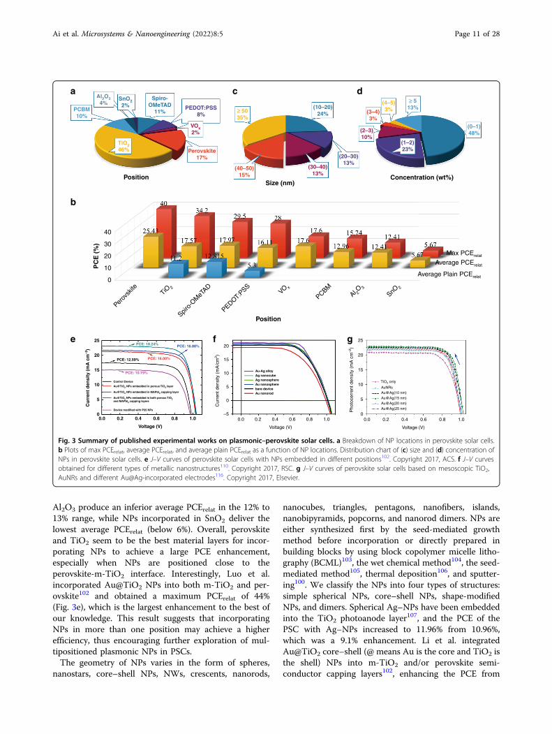
Al2O3 produce an inferior average PCErelat in the 12% to13% range, while NPs incorporated in SnO2 deliver thelowest average PCErelat (below 6%). Overall, perovskiteand TiO2 seem to be the best material layers for incor-porating NPs to achieve a large PCE enhancement,especially when NPs are positioned close to theperovskite-m-TiO2 interface. Interestingly, Luo et al.incorporated Au@TiO2 NPs into both m-TiO2 and per-ovskite102 and obtained a maximum PCErelat of 44%(Fig. 3e), which is the largest enhancement to the best ofour knowledge. This result suggests that incorporatingNPs in more than one position may achieve a higherefficiency, thus encouraging further exploration of mul-tipositioned plasmonic NPs in PSCs.The geometry of NPs varies in the form of spheres,
nanostars, core–shell NPs, NWs, crescents, nanorods,
nanocubes, triangles, pentagons, nanofibers, islands,nanobipyramids, popcorns, and nanorod dimers. NPs areeither synthesized first by the seed-mediated growthmethod before incorporation or directly prepared inbuilding blocks by using block copolymer micelle litho-graphy (BCML)103, the wet chemical method104, the seed-mediated method105, thermal deposition106, and sputter-ing100. We classify the NPs into four types of structures:simple spherical NPs, core–shell NPs, shape-modifiedNPs, and dimers. Spherical Ag–NPs have been embeddedinto the TiO2 photoanode layer107, and the PCE of thePSC with Ag–NPs increased to 11.96% from 10.96%,which was a 9.1% enhancement. Li et al. integratedAu@TiO2 core–shell (@ means Au is the core and TiO2 isthe shell) NPs into m-TiO2 and/or perovskite semi-conductor capping layers102, enhancing the PCE from
PCBM10%
SnO22%
Spiro-OMeTAD
11%PEDOT:PSS
8%
VOx2%
Perovskite17%
TiO246%
≥≥ 5035%
(40–50)15%
(30–40)13%
(20–30)13%
(2–3)10%
(3–4)3%
(4–5)3%
≥ 513%
(0–1)48%
(1–2)23%
(10–20)24%
Size (nm)Position
a c d
b
e 25
20PCE: 12.59%
PCE: 10.19%
PCE: 16.00%
PCE: 18.24% PCE: 16.88%
Cu
rren
t d
ensi
ty (
mA
cm
–2)
15
10
5
00.0 0.2 0.4 0.6
Voltage (V)
Control Device
Au@TiO2 NPs embedded in porous TiO2 layer
Au@TiO2 NPs embedded in MAPbl3 capping layer
Au-Ag alloyAg nanocubeAg nanosphereAu nanospherebare deviceAu nanorod
Au@TiO2 NPs embedded in both porous TiO2and MAPbl3 capping layers
Device modified with P25 NPs
0.8 1.0
Concentration (wt%)
Al2O34%
0.0 0.2 0.4 0.6
Voltage (V)
0.8 1.0
20
Cur
rent
den
sity
(m
A/c
m2 )
15
10
5
0
–50.0
TiO2 only
AuNRsAu@Ag(10 nm)Au@Ag(15 nm)Au@Ag(20 nm)Au@Ag(25 nm)
0.2 0.4 0.6
Voltage (V)
0.8 1.0
25
20P
hoto
cerr
ent d
ensi
ty (
mA
cm
–2)
15
10
5
0
f g
Max PCErelat
Average PCErelat
Average Plain PCErelat
40
30
PC
E (
%)
Position
20
10
0
Perov
skite
TiO 2
Spiro-
OMeT
AD
PEDOT:PSS
VO x
Al 2O 3
SnO2
PCBM
Fig. 3 Summary of published experimental works on plasmonic–perovskite solar cells. a Breakdown of NP locations in perovskite solar cells.b Plots of max PCErelat, average PCErelat, and average plain PCErelat as a function of NP locations. Distribution chart of (c) size and (d) concentration ofNPs in perovskite solar cells. e J–V curves of perovskite solar cells with NPs embedded in different positions102. Copyright 2017, ACS. f J–V curvesobtained for different types of metallic nanostructures110. Copyright 2017, RSC. g J–V curves of perovskite solar cells based on mesoscopic TiO2,AuNRs and different Au@Ag-incorporated electrodes116. Copyright 2017, Elsevier.
Ai et al. Microsystems & Nanoengineering (2022) 8:5 Page 11 of 28

12.59% (reference device without metal NPs) to 18.24%(Fig. 3e). Plasmonic Au nanostars have been incorporatedinto m-TiO2 for PSCs108, and the PSCs fabricated withTiO2–Au nanostars exhibited a PCE enhancement of16.66%, increasing from 15.19% to 17.72%. Ma et al.showed that Au nanorod–NP dimers could enhance thePCE of PSCs by 16%109. The NPs of simple spherical NPs,core–shell NPs, shape-modified NPs, and dimers allbrought about remarkable PCE enhancements. In parti-cular, the latter three structures brought about higherPCEs than simple spherical NPs.Materials such as Ag, Au, Au@SiO2, Ag@TiO2,
SiO2@Ag@TiO2, Au@Ag, Au–Ag alloy, Au@Pt@Au, andCu–Ag alloy were used to fabricate NPs. For instance, Au,Ag, and Au–Ag nanoalloy NPs with different sizes andshapes were embedded into the ETLs (TiO2) of PSCs viathe physical deposition method110. The Au–Ag nanoalloyshowed the best PCE improvement with a PCE = 14.8%,which was a PCE increase of 17.5% compared with barePSCs (Fig. 3f). Sun et al. applied AuAg@AuAg (AuAg)core–shell alloy NCs (ANCs) into the PEDOT:PSS layersof PSCs as a dopant111. The highest PCE of the deviceswith AuAg ANC-doped PEDOT:PSS was 16.76%, whichwas an increase of 28% compared with that of the deviceswithout AuAg ANCs (PCE = 13.14%). Chen et al.incorporated Cu–Ag alloy NPs to achieve a remarkableefficiency of 18.89%104. Au@Pt@Au core–shell NPs wereincorporated into PSCs112, which increased the PCE by8.1%, from 12.4% (normal PSCs without NPs) to 13.4%. Itshould be noted that NPs are usually coated by ligands(polyvinylpyrrolidone (PVP)) after the solution synthesisprocess107. Cho et al. replaced the original capping agent(PVP) with thermally stable propanethiol ligands by aligand exchange method, which can prevent the aggre-gation of Ag NPs in the perovskite active layer113. Thepropanethiol ligands can improve the optical and mor-phological properties and lead to a better dispersion of theAg NPs in the perovskite than that of the PVP-capped orbare Ag NPs. Regarding the core–shell structure, theshells can be SiO2
114 and TiO2115. Tang et al. demon-
strated that Au@SiO2 core–shell nanorods with opti-mized aspect ratios could greatly enhance theperformance of MAPbI3 PSCs114. Such structuresachieved a 16.1% improvement (from 12.4% to 14.4%) inthe maximal EQE and increased the maximal Jsc by 13.5%from 20.0 to 22.7 mA/cm2. The open voltage (Voc) andfilling factor (FF) remained almost the same. Core–shellAg@TiO2 NPs were added to PSCs by a low-temperatureprocessing route, enhancing the PCE up to 16.3%115. Ingeneral, the alloyed NPs show stronger enhancement.Figure 3c, d shows the distribution of the sizes and
concentrations of NPs that possess the largest PCEenhancement in each work. Approximately 90% of theworks fall in the size range of 10–50 nm and
concentration range of 0–5 wt%. Approximately half ofthe works use small NPs (<30 nm) and low concentrations(<1 wt%). Detailed results are presented to study the sizeeffect. Au@Ag nanocuboids with lengths of 10, 15, 20, and25 nm have been incorporated into an m-TiO2 layer,yielding PCEs of 16.89%, 17.21%, 16.35%, and 16.14%,respectively; these values correspond to relativeenhancements of 11.4%, 13.5%, 7.8%, and 6.5% (Fig. 3g),respectively116. Au@Ag nanocuboids with a diameter of15 nm show the best performance. Liu et al. investigatedthe effect of Ag NPs with diameters of 11 and 16 nm onthe performance of PSCs117. PSCs with different NPsshowed different Jsc, Voc, and FF values. Overall, the NPswith a diameter of 11 nm showed the largest PCE.Regarding core–shell NPs, the thickness of the shell isimportant. Pathak et al. investigated the effect of the shellthickness by coating Au NRs with 5 and 10 nm TiO2
shells118. The performance of all devices with theAu@TiO2 nanorods (NRs) improved, regardless ofthe TiO2 shell thickness. However, their underlyingmechanism for the performance enhancement was dif-ferent. The Jsc of the devices with the Au@TiO2 NRs thathad thicker shells remained the same, but their Voc
increased from 1.02 to 1.08 V compared with the deviceswithout the NRs. In contrast, regarding the devices withthinner shells, Voc remained unchanged, while Jsc exhib-ited an improvement from 20.68 to 22.23 mA/cm2. Par-ticular efforts have also been devoted to the concentrationeffect. Malireport et al. studied the effect of 0.1 wt% to 0.5wt% Au NPs in TiO2 on PSCs based on an in situsynthesis method of Au-embedded TiO2 nanofibers by anelectrospinning technique119. The PCE, Voc, Jsc, and FFincreased as the NP concentration was increased from 0.1wt% to 0.3 wt%; notably, these parameters decreased whenthe NP concentration was increased from 0.3 wt% to 0.5wt%, i.e., the devices with 0.3 wt% attained the highestperformance. Higgins et al. demonstrated planar PSCswith the structure ITO/PEDOT:PSS/MAPbI3/PCBM/Ni:Au, where PCBM was modified with variable amounts ofAg NPs (3, 5, 7, 10, 20, and 100 wt%)120. The addition of 5wt% Ag NPs showed the largest PCE enhancement of60.76%, increasing from 7.34% to 11.90%. Based on theabove analysis, the size and concentration have differenteffects on the current, voltage, and FF and thus need to beoptimized carefully to achieve the best performance.The underlying mechanism of plasmonic NPs in PSCs
was discussed in previous reports. The keywords arepresented in Table 1, including the LSPR, field enhance-ment, electron–hole separation, scattering, chargeseparation, light absorption, hot electron injection, andcarrier transport. At times, the explanations are confusingand even conflicting. Here, we attempt to provide acomprehensive and consistent summary of the mechan-isms by looking into the cause and effect, as shown in
Ai et al. Microsystems & Nanoengineering (2022) 8:5 Page 12 of 28
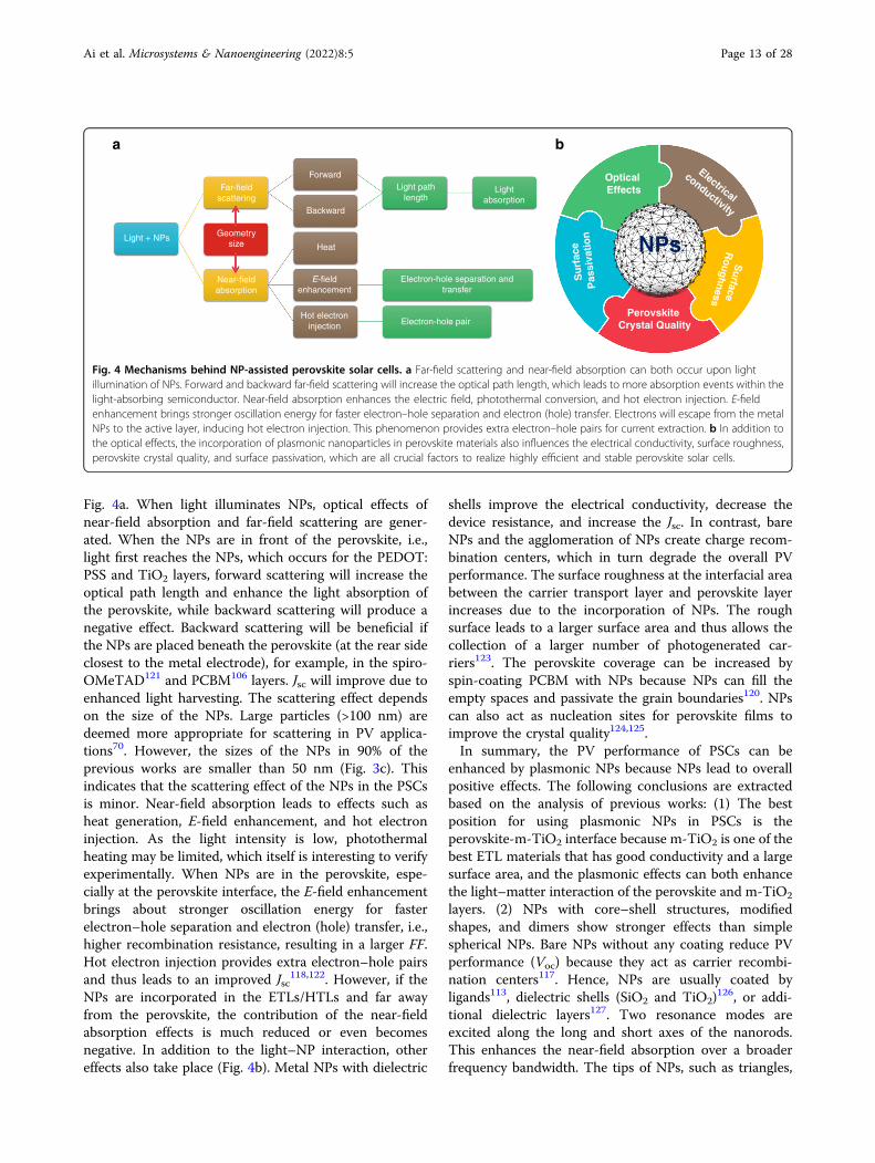
Fig. 4a. When light illuminates NPs, optical effects ofnear-field absorption and far-field scattering are gener-ated. When the NPs are in front of the perovskite, i.e.,light first reaches the NPs, which occurs for the PEDOT:PSS and TiO2 layers, forward scattering will increase theoptical path length and enhance the light absorption ofthe perovskite, while backward scattering will produce anegative effect. Backward scattering will be beneficial ifthe NPs are placed beneath the perovskite (at the rear sideclosest to the metal electrode), for example, in the spiro-OMeTAD121 and PCBM106 layers. Jsc will improve due toenhanced light harvesting. The scattering effect dependson the size of the NPs. Large particles (>100 nm) aredeemed more appropriate for scattering in PV applica-tions70. However, the sizes of the NPs in 90% of theprevious works are smaller than 50 nm (Fig. 3c). Thisindicates that the scattering effect of the NPs in the PSCsis minor. Near-field absorption leads to effects such asheat generation, E-field enhancement, and hot electroninjection. As the light intensity is low, photothermalheating may be limited, which itself is interesting to verifyexperimentally. When NPs are in the perovskite, espe-cially at the perovskite interface, the E-field enhancementbrings about stronger oscillation energy for fasterelectron–hole separation and electron (hole) transfer, i.e.,higher recombination resistance, resulting in a larger FF.Hot electron injection provides extra electron–hole pairsand thus leads to an improved Jsc
118,122. However, if theNPs are incorporated in the ETLs/HTLs and far awayfrom the perovskite, the contribution of the near-fieldabsorption effects is much reduced or even becomesnegative. In addition to the light–NP interaction, othereffects also take place (Fig. 4b). Metal NPs with dielectric
shells improve the electrical conductivity, decrease thedevice resistance, and increase the Jsc. In contrast, bareNPs and the agglomeration of NPs create charge recom-bination centers, which in turn degrade the overall PVperformance. The surface roughness at the interfacial areabetween the carrier transport layer and perovskite layerincreases due to the incorporation of NPs. The roughsurface leads to a larger surface area and thus allows thecollection of a larger number of photogenerated car-riers123. The perovskite coverage can be increased byspin-coating PCBM with NPs because NPs can fill theempty spaces and passivate the grain boundaries120. NPscan also act as nucleation sites for perovskite films toimprove the crystal quality124,125.In summary, the PV performance of PSCs can be
enhanced by plasmonic NPs because NPs lead to overallpositive effects. The following conclusions are extractedbased on the analysis of previous works: (1) The bestposition for using plasmonic NPs in PSCs is theperovskite-m-TiO2 interface because m-TiO2 is one of thebest ETL materials that has good conductivity and a largesurface area, and the plasmonic effects can both enhancethe light–matter interaction of the perovskite and m-TiO2
layers. (2) NPs with core–shell structures, modifiedshapes, and dimers show stronger effects than simplespherical NPs. Bare NPs without any coating reduce PVperformance (Voc) because they act as carrier recombi-nation centers117. Hence, NPs are usually coated byligands113, dielectric shells (SiO2 and TiO2)
126, or addi-tional dielectric layers127. Two resonance modes areexcited along the long and short axes of the nanorods.This enhances the near-field absorption over a broaderfrequency bandwidth. The tips of NPs, such as triangles,
Light + NPs Geometrysize
Near-fieldabsorption
Far-fieldscattering
E-fieldenhancement
Hot electroninjection Electron-hole pair
Electron-hole separation andtransfer
Light pathlength
Lightabsorption
Heat
Backward
Forward
a
Optical Effects
Electrical
conductivity
Surface
Roughness
Su
rfac
e
Pas
siva
tio
n
NPs
Perovskite Crystal Quality
b
Fig. 4 Mechanisms behind NP-assisted perovskite solar cells. a Far-field scattering and near-field absorption can both occur upon lightillumination of NPs. Forward and backward far-field scattering will increase the optical path length, which leads to more absorption events within thelight-absorbing semiconductor. Near-field absorption enhances the electric field, photothermal conversion, and hot electron injection. E-fieldenhancement brings stronger oscillation energy for faster electron–hole separation and electron (hole) transfer. Electrons will escape from the metalNPs to the active layer, inducing hot electron injection. This phenomenon provides extra electron–hole pairs for current extraction. b In addition tothe optical effects, the incorporation of plasmonic nanoparticles in perovskite materials also influences the electrical conductivity, surface roughness,perovskite crystal quality, and surface passivation, which are all crucial factors to realize highly efficient and stable perovskite solar cells.
Ai et al. Microsystems & Nanoengineering (2022) 8:5 Page 13 of 28
cubes, pentagons, and popcorns, provide more hotspotsthan spherical NPs, leading to stronger LSPR and near-field absorption. NP dimers with small gaps haveenhanced near-field absorption due to the stronger cou-pling between NPs. NPs with core–shell, dimer, and othermodified shapes also show stronger effects than simplespherical NPs. (3) The alloyed NPs show a larger PVenhancement than that of a single material because thecomposite materials can broaden the absorption spec-trum. (4) The size and concentration have different effectson the current, voltage, and FF and thus need to beoptimized carefully. The size of the NPs should be tunedto make the absorption of NPs fall within the solarspectrum and overlap as much as possible, especially inthe wavelength range where the intrinsic absorption of theperovskite is weak. Ultraviolet (UV) and NIR light can beabsorbed by controlling the size of the NPs. In addition,the thickness of the shell is important. The interactionbetween the near-field absorption and perovskite can bechanged due to the different shell thicknesses. When theshell is thick, the surface potential of the coating dielectriclayer is changed by hot electron injection. As a result, thebuilt-in potential of the device will increase118. The Voc
enhancement is not obvious once the shell is thinner thana certain threshold. In contrast, Jsc will be improved with athinner dielectric layer because the interaction betweenthe hot electrons from the metal and the excitons fromthe perovskite is strong and facilitates carrier separationand transport within the devices. A larger concentrationof NPs results in stronger absorption; however, this alsoleads to agglomeration and recombination centers119. Themajority of the NPs achieve a maximum PCE at a lowconcentration of <2 wt% (Fig. 3d). Based on the sum-marized results, we infer that alloyed core–shell nanorods(with sharp tips and sub-10 nm gaps) that are dispersed atthe perovskite-m-TiO2 interface show promise forachieving higher PV performance. The sizes and con-centrations may be optimal when <50 nm and <2 wt%,respectively.
Plasmonic film-assisted perovskite solar cellsPlasmonic films are defined here as corrugated struc-
tures such as periodic arrays or random distributions ofsubwavelength holes (nanoholes) perforated in a metalfilm128,129 and structured continuous films130,131 that canexcite the SPP mode or both the SPP and LSPR modes132.The plasmonic properties can be tuned by the film mor-phology, periodicity, and materials. The coupling betweenSPPs and LSPRs can result in unique optical effects andstronger light confinement. In addition, the penetrationdepth of SPPs into the dielectric can be 100 nm–1 μm,which is much larger than that of LSPR (<10 nm)133. Thismakes SPPs, in principle, able to exert a larger influence onthe perovskite layer, ETL or HTL, leading to a higher PCE.
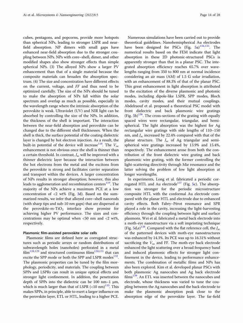
Numerous simulations have been carried out to providetheoretical guidelines. Nanohemispherical Au electrodeshave been designed for PSCs (Fig. 5a)134,135. Thenumerical results based on the FEM indicate that lightabsorption in these 2D photonic-structured PSCs isapparently stronger than that in a planar PSC. The inte-grated absorption efficiency reaches 65.7% over wave-lengths ranging from 350 to 800 nm at normal incidenceconsidering an air mass (AM) of 1.5 G solar irradiation,with an enhancement of 88.3% of that of the planar PSC.This great enhancement in light absorption is attributedto the excitation of the diverse plasmonic and photonicmodes, including dipole-like LSPR, SPP modes, Blochmodes, cavity modes, and their mutual couplings.Abdelraouf et al. proposed a theoretical PSC model withfront dielectric and back plasmonic wire gratings(Fig. 5b)136. The cross-sections of the grating with equallyspaced wires were rectangular, triangular, and hemi-spherical. The light absorption was the highest for Agrectangular wire gratings with side lengths of 110–150nm, and Jsc increased by 22.4% compared with that of theplanar structure. The Jsc of Ag triangular and semi-spherical wire gratings increased by 13.9% and 15.4%,respectively. The enhancement arose from both the con-tribution of the front dielectric wire grating and backplasmonic wire grating, with the former controlling thelight-scattering directivity through Mie resonance and thelatter solving the problem of low light absorption atlonger wavelengths.In experiments, Long et al. fabricated a periodic cor-
rugated HTL and Au electrode137 (Fig. 5c). The absorp-tion was stronger for the periodic microstructurecomposite HTL with the conformal Au electrode com-pared with the planar HTL and electrode due to enhancedcavity effects. Both Fabry–Pérot resonance and SPRplayed a role in the cavity, increasing the light-harvestingefficiency through the coupling between light and surfaceplasmons. Wei et al. fabricated a metal back electrode intoa moth-eye nanostructure via a soft imprinting technique(Fig. 5d,e)138. Compared with the flat reference cell, the Jscof the patterned devices with moth-eye nanostructureswas enhanced by 14.3%. Its PCE was up to 16.31% withoutsacrificing the Voc and FF. The moth-eye back electrodeenhanced the light scattering over a broad frequency bandand induced plasmonic effects for stronger light con-finement in the device, leading to performance enhance-ments. The combination of metallic films and NPs hasalso been explored. Kim et al. developed planar PSCs withboth plasmonic Ag nanocubes and Ag back electrodefilms139. An ETL was inserted between the nanocubes andelectrode, whose thickness was varied to tune the cou-pling between the Ag nanocubes and the back electrode tomake the plasmonic absorption peak close to theabsorption edge of the perovskite layer. The far-field
Ai et al. Microsystems & Nanoengineering (2022) 8:5 Page 14 of 28
scattering and near-field absorption around the nanocubeface closest to the perovskite layer were also greatlyenhanced by the coupling. The average PCE wasenhanced from 11.9% to 13.3% due to plasmonic coupling.Plasmonic films have not been used as widely as NPs
because the fabrication of corrugated plasmonic films inPSCs is usually more complex. In addition, the trans-mission of plasmonic films is low, so plasmonic films canonly be used on the rear side of PSCs. Nevertheless, thesepioneering works have shown the great potential ofplasmonic films to increase the efficiency of PSCs.
Plasmonic–perovskite light emittersEnhanced spontaneous emissionHalide perovskite materials exhibit strong spontaneous
emission, whose wavelengths can be tuned throughoutthe visible range by mixing halide anions. This makesperovskites a promising platform for creating efficient,low-cost and multicolor optoelectronic devices such asLEDs and displays. Incorporating plasmonic nanos-tructures into LEDs to induce coupling between excitons(i.e., electron–hole pairs bound by Coulombic interac-tions) and surface plasmons is a powerful strategy toenhance the performance of perovskite LEDs (Fig. 6a)140.In theory, if the energy of the excitons of perovskitematches the SP resonant energy, the two energies will
couple and enhance the scattering or free-space re-emission. This leads to an extra recombination pathway,which significantly increases the spontaneous radiationrate (Fig. 6b) and improves emission performance.The plasmonic effects on perovskite LEDs are studied
mainly based on NPs. Mokkath et al. calculated the opticalproperties of Au-doped all-inorganic CsPbX3 (X = Cl, Br,I) perovskite quantum dots (QDs) based on time-dependent density functional theory141. Their resultsconfirmed deep-level trap states induced by the Audopant, a significant absorption redshift, and the emer-gence of E-field hotspot regions. CsPbBr3@Ag hybrid NCswere synthesized by reacting CsPbBr3 NCs with AgX (X =Cl, Br, or I) powders in hexane142. Briefly, 2–5 nm Ag NPswere nucleated and attached randomly on the surface ofCsPbBr3 NCs. The PL intensity and emission lifetime ofthe CsPbBr3@Ag hybrid NCs were significantly enhancedand reduced, respectively, compared with those of pureCsPbBr3 NCs when illuminated by 400 nm light (Fig. 6c,d). The enhancement was mainly attributed to the plas-monic effects of the Ag NPs enhancing the absorbance ofUV or blue light. However, Ag adhesion deteriorated thesurface quality of the CsPbBr3 NCs and in turn under-mined the PLQY. Therefore, Ag adhesion has both posi-tive and negative effects on the PL of hybrid perovskiteQDs. To achieve an enhanced PL, the size and density of
Au
Perovskite
FTO
Glass
200 nm
(l) Planar (ll) Rectangle Grating (lll) Triangle Grating (lV) Circular Grating
200 nm
600 nm
100 nm
700 nm
80 nm
2 μμm
2 μm
5 μm
5 μm
4
4
33
22
10
1
700 nmLcube Ltriangle
Rsphere
TiO2
TiO2
CH3NH3Pbl3
CuSCN
Ag
3 μm
2
1
0
1
2
80 nm
3 μm
20
a b
d ec
10 PMC
r
r
Tg
Tc
T
Tz
0 x
P
SpiroP3HT
PMC Manager
Photon
Optical & electric enhancement
+
Hole
0
–10
J sc
(mA
/cm
2 )
–20
–30
–40
–500.0 0.2 0.4 0.6 0.8
Voltage (V)
1.0
0
–5 Flat
Grating
Moth–eye–10
–15
Cur
rent
den
sity
(m
A c
m–2
)
–20
–250.0 0.2 0.4 0.6
Voltage (V)
0.8 1.0
Fig. 5 Plasmonic film-assisted perovskite solar cells. a 3D schematic diagrams and cross-sectional view of the hole-conductor-free PSC with thenanohemispherical Au electrode. Adapted with permission135. Copyright 2019, SPIE. b 3D schematics of the simulated PSC models with planar films,rectangular wire gratings, triangular wire gratings, and circular wire gratings. Adapted with permission136. Copyright 2018, Elsevier. c Performancecomparison of PSCs with spiro-, P3HT, and periodic microstructure composite (PMC) HTLs. Adapted with permission137. Copyright 2016, RSC. Theinset shows the simulated light field distribution of the 3D PMC HTL/Au at 668 nm and the enhanced optical transmission due to the hole. d SEMand AFM images of the grating and moth-eye patterned PCBM layers. e J–V curves of the flat, grating, and moth-eye patterned PSCs. Adapted withpermission138. Copyright 2017, Wiley. The performance (Jsc and PCE) of the PSCs are improved by plasmonic films due to the great enhancement inlight absorption, which is attributed to the excitation of the diverse plasmonic and photonic modes, including dipole-like LSPR, SPP modes, Blochmodes, cavity modes, and their mutual couplings.
Ai et al. Microsystems & Nanoengineering (2022) 8:5 Page 15 of 28

Ag NPs need to be optimized so that the positive effect isstronger than the negative effect. Xu et al. reported aperovskite blue LED with Au NPs embedded in PEDOT:PSS143. The fluorescence intensity was improved by 3.8times. The maximum luminance and EQE reached ~1110cd/m2 and 1.64%, respectively.
Liu et al. placed disordered Au NRs underneath a film ofCsPbBr3 NCs144 and studied their emission performance.By using femtosecond laser pulses at 800 nm, amplifiedspontaneous emission (ASE) at approximately 523 nmwas excited by two-photon pumping. A narrow peak witha linewidth of 5 nm appeared with the pump fluence
1.0
0.8
0.6
LiF/AI
TPBi
perovskite
PEDOT:PSS
ITO/glass
NPB
Ag
rods
Inte
nsi
ty (
a. u
.)
lifetime (ns)
Time / ns
500 550
Wavelength (nm)
600
W/O Au
With Au
0.4
0.2
0 10 20 30 40
without Ag-rod
with Ag-rod
0 h
0.5 h
2 h
5 h
24 h
50
1.0
0.8
0.6
Nor
mal
ized
EL
Inte
nsi
ty (
a.u
.)
0.4
0.2
0.00 2 4 6 8 10 12 14
a
c
e f
d
b
20 nm
1400000 h0.5 h2 h5 h24 h
CsPbBr3
Ag
120000
PL
inte
nsi
ty
100000
80000
60000
40000
20000
450 500 550
Wavelength / nm
6000
Fig. 6 Plasmonic–perovskite light emitters with enhanced spontaneous emission. a TEM image of a cross-section, the correspondingschematic diagram, and the photographic image of the plasmonic–perovskite LED based on the Ag-CsPbBr3 system. Adapted with permission140.Copyright 2017, ACS. b PL lifetime of the perovskite CsPbBr3 nanocrystal layer with and without Ag rods. c PL intensity and (d) fitted time-resolvedphotoluminescence decay spectra of CsPbClxBr3−x@Ag hybrid nanocrystals obtained by reacting CsPbBr3 nanocrystals with AgCl for 0–24 h. The insetin (c) shows photographs of the CsPbBr3 nanocrystals and CsPbClxBr3−x@Ag hybrid nanocrystals at a reaction time of 24 h under 365 nm UV lightirradiation. The enhancement is mainly attributed to the enhanced absorbance of UV or blue light by the Ag-induced plasmonic near-field effect.Adapted with permission142. Copyright 2017, RSC. e Left image: schematic of the Au/p-NiO/CsPbBr3 QD/MgZnO/Au NP/n-ZnO/n+-GaNheterostructure LED. Right image: cross-sectional SEM image of the NiO/CsPbBr3 QD/MgZnO/Au NP/ZnO coaxial NWs. (f) EL spectra of the plasmonicPeLED with Au NP decoration and the reference device without Au NPs captured at 8.0 V. The insets present the corresponding emissionphotographs of an emitting unit (2 × 2 mm2). The electroluminescence enhancement is associated with the increased spontaneous emission rateand improved internal QY induced by exciton–LSPR coupling. Adapted with permission150. Copyright 2018, Wiley.
Ai et al. Microsystems & Nanoengineering (2022) 8:5 Page 16 of 28

reaching a low threshold of 0.65 mJ/cm2, owing to theplasmonic effects of Au NRs improving the emissiontransition rate. et al. precipitated Ag NPs and CsPbBr3perovskite QDs in borosilicate glass by the conventionalmelt-quenching method145. Part of Pb2+ was replaced byAg+ in the CsPbBr3 QDs, and the remaining Ag+, whichdid not react with Pb2+, was converted into Ag NPs.These Ag NPs enhanced the PL by 5 times for theCsPbBr3 QD-doped glasses, which was mainly due to theenhanced optical absorption and LSPR of the Ag NPs.Yun et al. proposed stretchable plasmonic templates of Auand Au/SiO2 NPs embedded in polymer to improve theluminescence of CsPbBr3 NCs146. The charge carrierimbalance due to hole trapping in the perovskite LEDswith naked NPs could be prevented by embedding Au orAu/SiO2 NPs in the polymer. The luminescence of theperovskite NC film on the template with Au/SiO2 NPsincreased by 54% compared with that of the perovskiteNC film on the reference (polymer film without metalNPs). The luminescence enhancement of Au/SiO2 NPswas ascribed to coupling to the LSPRs of the Au/SiO2 NPs.Li et al. studied the performance of perovskite QD
(PQD) films coupled to Ag NW networks (NWKs) with aspacer of polyvinyl alcohol (PVA) between the PQD filmand NWKs147. Compared with bare quartz, the PVAsubstrate significantly enhanced the emission intensitybut reduced the emission rate of PQD excitons. WhenNWK was introduced, the emission intensity and rateexhibited a maximum of 6-fold (average 3.4-fold) and2.4-fold (average 1.9-fold) increases, respectively, due toefficient NWK–PQD coupling. They further demon-strated a Purcell-enhanced emission rate in a hybridstructure of PQDs with plasmonic crystals at roomtemperature148. Colloidal PQDs, Ag nanocubes, and PVPhave been incorporated together into a device by che-mical assembly. The PL enhancement can be modified inboth the steady-state fluorescence and time-resolvedmeasurements by changing the PVP spacer thicknessand Ag nanocube surface density. The total fluorescenceintensity and emission rate demonstrate 3.5-fold and 4.5-fold enhancements, respectively.A plasmonic Au NR/CsPbBr3 QD film was fabricated
via spin-coating149. The PL intensity of the Au NR/CsPbBr3 QD film demonstrated a 2-fold enhancementcompared to that of the CsPbBr3 QD film without AuNRs. The CsPbBr3 QD film exhibited a lifetime decreasefrom 6.15 ns to 4.78 ns after incorporating Au nanorods.The Au nanorods triggered an LSPR of approximately 500nm, which enhanced the emission intensity of theCsPbBr3 QD film. Shi et al. fabricated a Au/p-NiO/CsPbBr3 QD/MgZnO/Au NP/n-ZnO/n+-GaN hetero-structure LED (Fig. 6e, f)150. The emission was enhancedby 1.55 times after embedding Au NPs into the device.
The luminance, EQE, and current efficiency of the opti-mized plasmonic–perovskite LED reached 10206 cd/m2,~4.626%, and 8.736 cd/A, respectively. The electro-luminescence performance was enhanced due to theincreased spontaneous emission rate and improvedinternal QY, which was induced by the coupling betweenthe exciton and LSPR.Plasmonic films can also enhance the PL. Chen et al.
placed CsPbBr3 nanoplatelets between Ag NWs and a Agfilm. Strong biexciton emission was induced withcontinuous-wave excitation at room temperature151. Theexciton occupancy for generating biexcitons was reducedby ~106 times in the Ag NW-Ag film nanogaps. Thenonlinear Fano resonance between biexcitons and plas-monic cavity modes was responsible for the greatenhancement in biexciton emissions. Adamo et al.coated MAPbI3 on a Au slit film152. The luminescenceintensity was enhanced by more than 10 times comparedwith that of pure MAPbI3, while the luminescence life-time demonstrated a nearly 3-fold decrease. Theimprovement in luminescence intensity was attributed tothe significantly enhanced Purcell effect with anenhancement factor of more than 300.Plasmonic NPs and films with Au and Ag materials have
been used in perovskite LEDs and have achievedimpressive PL and EQE enhancements. It is expected thatmore nanostructures and different material combinationswith stronger plasmonic enhancement will be exploredfor perovskite LEDs. The impact of the plasmonicnanostructure on the crystal quality and stability shouldalso be studied more thoroughly.
Plasmonic–perovskite lasersThe properties of plasmonic-based perovskite lasers,
such as the threshold, wavelength, polarization, and laseremission characteristics, can be facilely controlled by therational design of the coupling between perovskites andplasmonic nanostructures. Plasmonic lasers with a lowmode volume have been realized by coupling the per-ovskite with plasmonic NPs and films. This progressadvances the development of high-performance per-ovskite micro/nanolasers.NPs have been used for plasmonic–perovskite lasers.
Wang et al. demonstrated plasmonic-enhanced laseremissions from all-inorganic lead-halide perovskites153.Uniform Al NPs were deposited onto the top surface ofCsPbBr3 perovskites by electron beam evaporation. Theresonance of the Al NPs was tuned to the emissionwavelength range of CsPbBr3 to enhance the PL. A 20%reduction in the thresholds of whispering gallery modelasers in CsPbBr3 perovskite microrods was observed. Theplasmonic effects enhanced the output intensities of per-ovskite microlasers by more than an order of magnitude.Huang et al. demonstrated the plasmonic–perovskite laser
Ai et al. Microsystems & Nanoengineering (2022) 8:5 Page 17 of 28
by placing MAPbX3 perovskite nanosheets on Au patternswith a 10 nm SiO2 spacer (Fig. 7a)
154. Whispering gallerymodes were successfully excited by Au substrates withcircle and grating patterns. Resonances within the hybridplasmonic nanolaser could be precisely controlled by theshape and size of the bottom Au patterns instead of thetop semiconductors, revealing the substrate-control con-cept. The standard wavelength deviation was as small as0.3 nm. The emission wavelengths could be tuned within a200 nm wavelength span by varying the stoichiometry ofthe perovskite. Hybrid plasmonic nanolasers were gener-ated, leading to lasing even with a small perovskitethickness (<40 nm) (Fig. 7b). Li et al. used Ag NWs asnucleation centers for growing perovskites, constructing aperovskite/Ag heterostructure (Fig. 7c)155. Low-thresholdlasing was achieved because the perovskite crystals notonly were a gain medium but also formed an opticalresonant cavity. The lasing modes could be modulated bytuning the plasmonic effects on the perovskite micro-cavities. Wu et al. placed a polymethyl methacrylate(PMMA) spacer layer and a Au NR-doped PMMA top
layer on perovskite thin films156. The ASE threshold andintensity of the perovskite with Au NRs demonstrated an~36% decrease and 13.9-fold increase, respectively, com-pared to those of perovskite films without Au NRs. Theenhancement was ascribed to both the contribution ofsurface passivation due to PMMA and the plasmoniceffects of Au NRs. Chen et al. introduced a detachable AlNP substrate to enhance MAPbBr3 perovskite lasing per-formance157. The lasing threshold and stimulated emissionof the Al-MAPbBr3 hybrid system were dramaticallyreduced by more than 27% and improved by 10 times,respectively, due to the plasmonic effects of the Al NPs.Hsieh et al. fabricated perovskite lasers based on theconfiguration of Ag nanocube/CsPbBr3 quantum dot/Al2O3/Au. CsPbBr3 quantum dots were placed in thenanogap between the Ag nanocube and Au film. Thethreshold decreased to 1.9 W/cm2 at 120 K, which wasdue to the ultrasmall mode volume and significant Purcellenhancement at the corner of the nanocavity inside thegap158. Lu et al. reported upconversion lasing based on theconfiguration of a single MAPbBr3 perovskite nanocrystal
glass substratePerovskite(CH3NH3Pbl3)
PMMAspacer
a b c
d e f
Ag substrate 4.4
0
30
60
90
120
50 100 150
Perovskite Thickness (nm)
200
Photonic mode
glass20 nm10 nm5 nm
τ1 = 1.1 ns
τ2 = 0.8 ns
τ3 = 0.2 ns
τ4 = 0.1 ns
Plasmonic mode
250 300 350
Nor
mal
ized
inte
nsity
(a.
u.)
Thr
esho
ld (
μJ/c
m2 )
4.8
Time (ns)
5.2
SiO2
y
x
z
MAPbBr 3 N
anowire
dG
Ag thin film
excitation beamλ = 355 nm
MAPbl3
AuSiO2
Si
Fig. 7 Plasmonic–perovskite lasers. a Schematic of a spaser (surface plasmon amplification by stimulated emission of radiation) composed of aMAPbI3 NP/SiO2/Ag plasmonic laser. Inset: SEM image of perovskite NPs lying on Au/SiO2 microdisks. In contrast to previous reports, here, the spasersare determined by the boundary of Au patterns instead of the crystal facets of MAPbX3 nanosheets. As a result, whispering gallery mode-basedcircular spasers and spaser arrays are successfully realized by patterning the Au substrate into circles and gratings, respectively. b Lasing threshold ofplasmonic and photonic lasers versus perovskite thickness; the solid lines are used for guidance. Only the hybrid plasmonic mode exists below aperovskite thickness of 40 nm. Adapted with permission154. Copyright 2018, ACS. c SEM image of a perovskite/Ag heterostructure. Insets: AFM imageand corresponding cross-sectional profiles of a typical heterostructure. The perovskite crystals can serve as both the gain medium and the opticalresonant cavity for low-threshold lasing. Adapted with permission155. Copyright 2016, ACS. d Schematic layer structure of the perovskites cappedwith a dielectric PMMA spacer and a Ag thin film. Not only can perovskite be protected from hydrolysis but also the lasing thresholds can be greatlyreduced due to the plasmonic effect. Adapted with permission161. Copyright 2016, OSA. e Schematic of a hybrid plasmonic microcavity structure. AMAPbBr3 nanowire sits on a SiO2/Ag substrate (∼ 50 ± 1 nm) with a spacer layer of SiO2 (dG ≈ 5 − 20 ± 1 nm). The exciton–photon coupling strengthis enhanced by ~35% on average, which is mainly attributed to surface plasmon-induced localized excitation field redistribution. f Time-resolved PLspectra of MAPbBr3 NWs sitting on glass and SiO2/Ag substrates with SiO2 thicknesses of 20, 10, and 5 nm. Adapted with permission162. Copyright2018, ACS.
Ai et al. Microsystems & Nanoengineering (2022) 8:5 Page 18 of 28

(PNC)/Al2O3/TiN/silicon159. TiN served as a resonance-adjustable plasmonic nanocavity and generated stronglocalized electromagnetic fields. Both the two-photonpumping rate and emission rate were enhanced by theplasmonic resonances and enabled the upconversion las-ing action. The lasing threshold decreased to 10 μJ/cm2,which was at least 3 orders of magnitude smaller than thethreshold of the reference sample (a PNC on silicon).Huang et al. demonstrated a hybrid plasmonic surfacelattice resonance (SLR) laser consisting of a MAPbBr3perovskite thin film on an Ag NP array160. The SLR modecould be tuned to couple the green light emission of theperovskite material by the design of the NP parameters,thus enhancing the lasing performance. The pumpingthreshold was approximately 0.54 μW, and the linewidthof the lasing signal was only 0.28 nm.The effects of plasmonic films on the perovskite laser
performance have also been studied. Lasing performanceis enhanced in lead-halide perovskites covered withPMMA and Ag (Fig. 7d)161. The PMMA layer can provideprotection from hydrolysis in the ambient environment.The lasing threshold can be reduced by more than twoorders of magnitude compared with that of bare per-ovskite because of the strong exciton–plasmon couplingbetween the Ag and perovskite films. Shang et al. reportedstrong exciton–photon interactions in MAPbBr3 per-ovskite NWs (Fig. 7e)162. Characteristic anticrossingbehaviors were observed near the exciton resonance inthe hybrid perovskite NW/SiO2/Ag cavity at room tem-perature, which indicated a Rabi splitting energy up to~564 meV. The exciton–photon coupling strength wasimproved by ~35% on average, which was mainly ascribedto the near-field redistribution induced by the plasmonicresonances. Compared with that of the NW directly onthe glass substrate, the spontaneous emission rate wasenhanced by 11, 5.5, and 1.4 times with SiO2 thicknessesof 5, 10, and 20 nm, respectively (Fig. 7f). Yu et al.reported a plasmonic–perovskite laser by placing per-ovskite NWs on an Ag substrate, where an insulatingspacer layer was inserted163. Relatively low threshold(13.5 μJ/cm2) operation was obtained under ambientconditions, and the devices worked well even at tem-peratures up to 43.6 °C. Wu et al. realized plasmoniclasing with a threshold down to ~6.5 μJ/cm2 at roomtemperature using CsPbBr3 NW-based plasmonic devi-ces164. Polarization-sensitive pump responses andhighly polarized emission parallel to the NW axis wereobserved due to the plasmonic modes. The Purcell effectreduced the radiative recombination lifetime of CsPbBr3NWs by a factor of ~6.14. The lasing threshold of theplasmonic device increased as the NW length becamelarger. This may make plasmonic devices smaller andmore integrated than conventional photonic devices.S. Yang et al. demonstrated an ultrafast nanolaser based
on a triple-layer structure of perovskite/MgF2/Ag filmproduced with a scalable solution method165. The emis-sion dynamics were accelerated by the strong plasmonicconfinement of the laser modes due to the couplingbetween the perovskite emission and SPs. Single-modelasing behavior was clearly observed at room temperature.The plasmonic–perovskite laser not only reduced thedevice size but also significantly promoted the emissionefficiency. Wang et al. studied the laser performance of asingle CH3NH3PbBr3 nanowire on a silver film withoutany insulating layer166. The nonhybridized plasmonicnanowire lasers exhibited ultrafast lasing dynamics withan approximately 1.9 ps decay rate and a 1 ps peakresponse time. The low threshold was due to the ultraflatsingle-crystal silver films and high-quality single-crystalperovskite nanowires.Plasmonic–perovskite lasers show great potential for
use in integrated optics due to their small size, lowthreshold, and controlled wavelength and polarization.The Purcell effect can be enhanced by plasmonic reso-nances, which increases the light–matter interaction andemission intensity while reducing the emission lifetime,thus enabling faster lasers and faster LEDs. Future chal-lenges include the ability to achieve efficient carrierinjection and the realization of an electrically pumpedplasmonic–perovskite laser. In addition, smarter nanos-tructures and plasmonic–perovskite interface designs areneeded to further reduce the device size and footprint, aswell as reduce the lasing threshold.
Plasmonic–perovskite sensorsPlasmonic–perovskite photodetectorsThe performance of PDs can be improved by plasmonic
nanostructures because they enhance the couplingbetween incident light and the semiconducting materialsthat generate photocurrents. In the work of Dong et al.,Au NCs were incorporated into CsPbBr3 NC visible-lightPDs167. The PDs with Au NCs exhibited a higher sensi-tivity with an on/off ratio that was more than one order ofmagnitude larger than that of the initial device at a 2 Vbias under 532 nm laser illumination (4.65 mW/cm2).Moreover, the photocurrent increased by 238% (from theoriginal 245.6 μA to 831.1 μA) with the incorporation ofAu NCs due to the near-field plasmonic enhancement. B.Du et al. fabricated an organic-inorganic hybrid per-ovskite PD with periodic Au nanosquares (Fig. 8a–d)168.The maximum EQE of this PD was up to 65%, which was2.5-fold higher than that of a similar hybrid perovskiteplaced on a usual Si/SiO2 substrate without Au nanos-quares. The large, localized E-field induced by the SPR ofAu nanostructures was responsible for the enhancement.With a configuration similar to that in Fig. 8a, Gu et al.studied the effect of Au nanotriangles on PD perfor-mance169. The EQE of MAPbI3-Au was ~3 times higher
Ai et al. Microsystems & Nanoengineering (2022) 8:5 Page 19 of 28
than that of the MAPbI3 film without Au nanotriangles.The photoresponsivity of the MAPbI3-Au-based PD was51 mA/W at 10 V with a power density of 1.5 W/cm2 andan EQE of 12.6% for an illumination wavelength of 450nm. Au NPs were integrated into the graphene/MAPbI3hybrid PDs (Fig. 8e, f)170. The device with Au NPsexhibited a 2-fold higher photoresponsivity and a fasterphotoresponse speed compared with those of pristinegraphene-MAPbI3 devices. Plasmon-enhanced light har-vesting was improved on the perovskite–graphene inter-face, which led to a higher PD operation speed and carrierextraction efficiency than devices without Au NPs. Ghoshet al. reported an air-processed high-performance self-powered hybrid perovskite PD whose ETL was embeddedwith plasmonic Ag NPs171. At zero bias, the ETL-free AgNP-perovskite hybrid device showed a ∼45% enhancedresponsivity and operated with a ∼3 times faster photo-response than the pristine device. The enhancementswere due to a series of positive effects introduced by theplasmonic Ag NPs, such as enhanced light absorption,hot electron generation, and improved charge extractionand transport.Ji et al. showed a quasi-2D perovskite PD with SiO2-
coated AuAg-alloyed nanoprisms (AuAg-NPrisms@SiO2)between the PEDOT:PSS and perovskite layers172.
The PDs with AuAg-NPrisms@SiO2 exhibited a high EQEof 1670% at a low driving voltage of −0.3 V. Theirresponsivity and detectivity reached 7.15 A/W and 3.2 ×10¹³ Jones, which were 51.2% and 68.4% higher than thoseof PDs without NPs. The enhancement was because theAuAg-NPrisms@SiO2 led to high-quality crystalline quasi-2D perovskite films and stronger light absorption in theactive layer, accelerating exciton dissociation at the inter-face and facilitating charge transport. Li et al. reported aPD composed of perovskite/Al NP/anodic aluminumoxide (AAO)173. The hybrid plasmonic–perovskitenanostructures showed a 43-fold increase in the photo-current, which was due to the enhanced E-fields aroundthe Au NPs. Wang et al. used plasmonic bowtie nanoan-tenna arrays to boost the performance of a perovskitePD174. The photoresponse and detectivity of theplasmonic–perovskite PD increased by ~2962% and morethan 30 times compared with those of a Si/SiO2-basedconventional PD, respectively. Electric fields were greatlyenhanced around the bowtie nanoantenna arrays due tothe LSPR effect, which led to the improvement. La et al.realized a perovskite PD by embedding assembled Au NPsin the PEDOT:PSS layer175. Charge extraction/transportand optical absorption were enhanced by the assembledAu NPs due to the good conductivity and plasmonic
0
PETOPCs500 nm
500 nm1 μμm
20 μm
10 20
(110)
a
c dg
e f
h
b
Au squares
Electrode
(112)
(220)
(310) (330)
XRD
30 40
2θ (Degree)
50 60
Au
Au
CH3NH3Pbl3
Graphene
VG = 0 V
VDS = 0.1 V
VDS = 10 V
R ∝ P –0.80
R ∝ P –0.75
CH3NH3Pbl3+Graphene+Au-NPs
CH3NH3Pbl3+Graphene
Au-NP
SiO2
Source/Drain
p+ Si
Ag NCs
CsPbCl3 NCs layer
10–11
10–10
10–9
10–8
10–7
100 200
Light intensity P (W/cm2)
Res
po
nsi
vity
(A
/W)
10–510–2
10–1
100
101
102
103
10–4 10–3
Time (s)
Cur
rent
(A
)
300 400
CsPbCl3
CsPbCl3 on Ag/OPCs
Fig. 8 Plasmonic–perovskite photodetectors. a–d Organic-inorganic hybrid perovskite PD on arrays of Au nanostructures. The maximum EQE ofthis PD is as high as approximately 65%, 2.5 times that on a usual Si/SiO2 substrate without Au nanostructures, which is due to the large, localizedE-field induced by the SPR. a Schematic of the device on a plasmonic substrate. b SEM images of the plasmonic substrate. c The dependence of thephotocurrent on the incident laser power for the device on Si/SiO2 and plasmonic substrates at zero bias. d EQE of devices on Si/SiO2 and plasmonicsubstrates. Adapted with permission168. Copyright 2019, Wiley. e, f Graphene/MAPbI3 hybrid PDs integrated with Au NPs. e Schematic of the Au NP/graphene/CH3NH3PbI3 hybrid PDs. f Responsivities versus light intensity at different VDS biases. The dependencies of the responsivities on the lightintensity are fitted with power functions with the listed fitting parameters. Compared with pristine graphene-MAPbI3 devices, this device has twotimes higher photoresponsivity and a faster photoresponse speed. This enhancement can be attributed to the improved light absorption in theperovskite layer due to the plasmonic effect of the Au NPs. Adapted with permission170. Copyright 2016, RSC. g, h CsPbCl3/Ag/OPC hybrid PDs. (g)Schematic of CsPbCl3 on Ag/OPC PDs. h On-off switching properties measured under 365 nm light illumination (10 mW/cm2) at a bias of 3 V. Thephotocurrent of CsPbCl3 PD with Ag/OPC is 682% higher than that of CsPbCl3 PD without Ag/OPC. Adapted with permission176. Copyright2018, Wiley.
Ai et al. Microsystems & Nanoengineering (2022) 8:5 Page 20 of 28
resonance of the Au NPs. The responsivity, noise equiva-lent power (NEP), and response speed of the perovskitewith Au NPs were ~2063 A/W, ~1.93 × 10⁻¹⁴ W/Hz1/2,and ~300 ns, respectively, which were approximately 4.1-,15.6-, and 2.8-fold increases, respectively, compared withthose of a perovskite PD without NPs.Ag films composed of Ag NCs and CsPbCl3 NCs were
used for high-performance flexible ultraviolet photo-detectors (Fig. 8g, h)176. The luminescent intensityenhancement of the CsPbCl3 NCs showed a more than150-fold improvement with an estimated emission effi-ciency of 51.5%. The improvement was due to thecombined excitation and emission field enhancement.The CsPbCl3/Ag/opal photonic crystal (OPC) hybridsexhibited a dark current of 10–11 A, detectivity of 9 ×10¹⁴ Jones, response time of 28 ms, and response line-width of 30 nm. This performance was claimed to exceedthat of commercial silicon PDs at the time that the paperwas published.By integrating plasmonic nanostructures with per-
ovskites, enhanced light absorption can be attained, whichopens the door for high-performance photodetectors.Moreover, plasmonic metals can also act as electrodes andperform carrier extraction without increasing the com-plexity of the configuration. The challenge will be to avoidcarrier tunneling between metals and perovskite andsimultaneously increase the conductivity. Different com-binations of halide perovskite materials and plasmonicnanostructures should be explored to maximize photo-detector performance across the desired wavelength span.
Plasmonic–perovskite optical sensorsRecently, halide perovskites have been explored for
applications as refractometric sensors, surface-enhancedRaman scattering (SERS), and biologic sensors. Elshor-bagy et al. theoretically reported a perovskite refracto-metric sensor with an extruded array of high aspect-ratiodielectric pyramids, which excited SPRs at its frontsurface by grating coupling with the metal surface177.The generated photocurrent acted as the sensing signal,where selective absorption with a spectral responsenarrower than 1 nm was achieved. Without relying onthe spectral acquisition scheme, the perovskite devicerefractometric sensor used an optoelectronic interroga-tion method. The device showed considerable sensingperformance in the refraction index range between 1.0and 1.1. The figure of merit (FOM) could reach 1005RIU−1. In addition, the perovskite refractometric sensoralso possessed the advantages of a simple signal acqui-sition procedure and low cost.Qiao et al. demonstrated a superficial-layer-enhanced
Raman scattering (SLERS) technique for detecting speciesthat were noninteractive with Raman substrates. Theconfiguration consisted of elongated tetrahexahedral
Au NP (ETHH Au NP) arrays covered with a superficialCH3NH3PbBr3 film (Fig. 9a, b)178. These ETHH NP arraysprovided uniform and high-density SERS hotspots, andthe perovskite film acted as a dielectric media to slow theattenuation of the electromagnetic evanescent wave of thehotspots, which made SLERS occur in the superficial layerrather than just on the surface of the ETHH Au NPs. Zenget al. presented a sensor based on a hybrid metasurfaceconsisting of 2D perovskites and metal thin films179. Thedevice showed a sharp optical phase change and a Goos-Hänchen shift around the wavelength of the SPP (Fig. 9c).The Goos-Hänchen (GH) shift exhibited a sensitivity of900,000 μm/RIU, which was more than 4 orders ofmagnitude higher than that of a pure Ag sensing substrate(800 μm/RIU) (Fig. 9d). When silver nanogrooves wereused (Fig. 9e), coupling between the LSPR and SPP wavesled to a deeper dip in the angular spectra, implying afurther improvement in the detection sensitivity. Such 2Dperovskite-based metasurfaces show promise for use asultrasensitive in situ biosensors.Halide perovskites have not been widely studied as
sensors; thus, reports of plasmonic–perovskite sensors arerarer. Nevertheless, plasmonic sensors are a maturetechnology with numerous chemical, biological andmedical detection applications. The combination ofplasmonics and perovskite technologies will break newboundaries in sensitivity and pave the way for a trulycompact and integrated optical sensor platform. We alsoenvision the use of plasmonic–perovskite sensors todetect other physical and environmental parameters indifferent technological domains.
Other plasmonic–perovskite applicationsThe performance of perovskites in photocatalysis can
also be enhanced by plasmonic NPs. Ag NPs have beensynthesized on perovskite orthorhombic KNbO3 NWs byfacile photoreduction180. Ag/KNbO3 nanocomposites withdifferent Ag contents (0.4–2.8 wt%) have been used tomonitor the degradation of aqueous rhodamine B underUV and visible light. As the Ag content is increased,the UV-induced photoreactivity first increases, reaching amaximum at a Ag content of ~1.7 wt%, and thendecreases. The maximum photoreactivity is ~13-foldhigher than that of pristine KNbO3 without Ag NPs. Incontrast, visible light-induced photoreactivity shows amonotonic positive correlation with Ag contents from 0.4wt% to 2.8 wt%. Saris et al. used CsPbBr3 NC/AlOx
composite films with Ag NCs to drive chemical reactionsbased on the coupling between perovskite and Ag NCs(Fig. 10a, b)181. It was found that energy migrated from theperovskite NCs toward the Ag NCs. This energy migrationwas utilized to boost plasmon-mediated methylene bluedesorption, in which coupling to the perovskite NCsenhanced the spatial and spectral absorption of the
Ai et al. Microsystems & Nanoengineering (2022) 8:5 Page 21 of 28

chemical reaction. Chanana et al. proposed a triple-layeredstructure of (C6H5C2H4NH3)2(CH3NH3)n−1(PbI4)n/MAPbI3/Al hole arrays/silicon substrate (Fig. 10c) for thephotoinduced modulation of THz resonance182. Thesample with n = 1 showed a distinct THz transmissionpeak, exhibiting no optical intensity dependence whenilluminated at 700 nm (Fig. 10d), since that wavelength didnot correspond to photogenerated excitons in the per-ovskite layer. When the samples were illuminated in thewavelength range where excitons were formed, theincreased THz absorption within the holes led to loweroverall THz transmission with increasing optical intensity(Fig. 10e–g). This work indicated that the plasmonic effectcould be tuned by the perovskite. Zhou et al. reported apolarization-dependent modulation based on hybrid per-ovskite plasmon-induced transparency (PIT)183. AMAPbI3 film was coated on the PIT acting as a photo-active medium. Even with ultralow laser fluence pumping,a significant reduction in PTI transmission was observed
for the two polarizations at 0.86 and 1.12 THz with arecovery time of 561 ps, demonstrating the high sensitivityand ultrafast modulation speed of the device.
Conclusions and outlookIn recent years, researchers have demonstrated the use
of plasmonics to enhance the performance of perovskite-based solar cells, light emitters, photodetectors, sensors,and many other applications. Regarding plasmonic PSCs,the majority of studies are based on NPs because NPs canbe synthesized and easily incorporated into devices. Weobserved several trends from the vast amount of literatureon NP-assisted PSCs that we examined: (1) the PCE ofPSCs can be significantly enhanced by plasmonic NPs; (2)PSCs with plasmonic NPs incorporated at the perovskite-m-TiO2 interface or simultaneously at multiple positionscan potentially achieve the largest PCE enhancement; (3)NPs with a core–shell structure, shape modification, anddimer show stronger effects than that of simple spherical
a bModel 1Model 2Model 3Model 4
400 800 1200 1600Model 3 Model 4
Model 1
BααP
Model 2
Raman shift (cm–1)
Inte
nsi
ty(a
.u.)
Perovskite
ETHH array
Si substrate200 nm
c d2.5×104
Goos–Hänchen shift
TM
TELCH
Lshift k1 ��TM
�θ
priam
θSPA
Ag
2
1.5
GH
sh
ift
(μm
) Ph
ase (deg
)
1
0.5
054 54.1 54.2 54.3 54.4 54.5 54.6 54.7
Angle of incidence (deg)
00
2
4
6
8
10
12
14
16
181.5
× 10–5
1.2
0.9
0.6
0.3
0
0.2 0.4 0.6 0.8 1
Pure Ag thin filmOptimized FAPbI3/Ag film
1.2
Refractive-index change of biomolecules layer (10–8RIU)
Cha
nge
in G
H s
hift
(μm
)
–100
–50
0
50
100
–150
e 0.04
0.03
0.02
Ref
lect
ion
0.01
0.0055.2 55.4 55.6
Incidence Angle (deg)
10 nm
20 nm
30 nm
40 nm
50 nm
60 nm
55.8 56.0
Fig. 9 Plasmonic–perovskite optical sensors. a, b Superficial-layer-enhanced Raman scattering (SLERS) technique based on covering elongatedtetrahexahedral (ETHH) Au NP arrays with a CH3NH3PbBr3 film. Noninteracting analytes, such as benzo[α]pyrene (BαP) that has chronic toxicity andcan easily adhere to human skin or muscles to cause carcinogenesis, is detected. a Cross-sectional SEM images of the perovskite film on ETHH NParrays. b Raman spectra of BαP in four different models without (Model 1 and Model 2) and with (Model 3 and Model 4) the perovskite. BαP issegregated from the ETHH arrays by n-alkyl thiols in Model 2 and Model 4. The Raman signals are significantly enhanced with the perovskite becausethe perovskite film, as a dielectric medium, slows the attenuation of the electromagnetic evanescent wave and the LSPR decay is suppressed alongthe vertical direction away from the nanostructured surface. Adapted with permission178. Copyright 2019, Wiley. c Optical phase and GH shift as afunction of the angle of incidence near the SPP resonance angle of 54.36°. The sensing substrate consists of a bilayer FAPbI3 on a 45-nm silver thinfilm. d Simulations showing that a plasmonic sensor based on graphene/FAPbI3/hBN/Ag can detect small refractive index changes on the order of10–8 RIU, which is 4 orders of magnitude more sensitive than plasmonic sensors based on a simple Au substrate. The presence of 2D perovskite layersof a suitable thickness can lead to deeper SPP resonance dips, which correspond to a sharper optical phase change and a larger GH shift. e Simulatedangular reflectance spectra for a device consisting of bilayer FAPbI3 on silver nanogrooves with various groove widths. The insets show that theenhanced near fields lead to deeper spectral dips. Adapted with permission214. Copyright 2020, MPDI.
Ai et al. Microsystems & Nanoengineering (2022) 8:5 Page 22 of 28
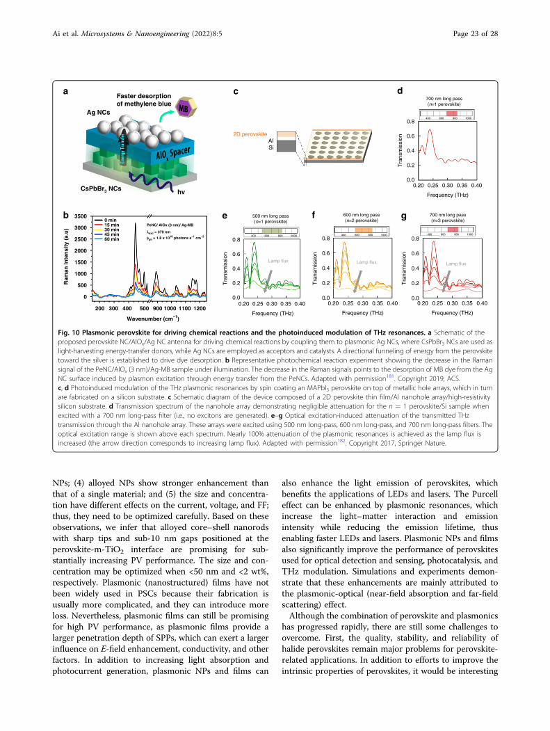
NPs; (4) alloyed NPs show stronger enhancement thanthat of a single material; and (5) the size and concentra-tion have different effects on the current, voltage, and FF;thus, they need to be optimized carefully. Based on theseobservations, we infer that alloyed core–shell nanorodswith sharp tips and sub-10 nm gaps positioned at theperovskite-m-TiO2 interface are promising for sub-stantially increasing PV performance. The size and con-centration may be optimized when <50 nm and <2 wt%,respectively. Plasmonic (nanostructured) films have notbeen widely used in PSCs because their fabrication isusually more complicated, and they can introduce moreloss. Nevertheless, plasmonic films can still be promisingfor high PV performance, as plasmonic films provide alarger penetration depth of SPPs, which can exert a largerinfluence on E-field enhancement, conductivity, and otherfactors. In addition to increasing light absorption andphotocurrent generation, plasmonic NPs and films can
also enhance the light emission of perovskites, whichbenefits the applications of LEDs and lasers. The Purcelleffect can be enhanced by plasmonic resonances, whichincrease the light–matter interaction and emissionintensity while reducing the emission lifetime, thusenabling faster LEDs and lasers. Plasmonic NPs and filmsalso significantly improve the performance of perovskitesused for optical detection and sensing, photocatalysis, andTHz modulation. Simulations and experiments demon-strate that these enhancements are mainly attributed tothe plasmonic-optical (near-field absorption and far-fieldscattering) effect.Although the combination of perovskite and plasmonics
has progressed rapidly, there are still some challenges toovercome. First, the quality, stability, and reliability ofhalide perovskites remain major problems for perovskite-related applications. In addition to efforts to improve theintrinsic properties of perovskites, it would be interesting
a c
AISi
2D perovskite
d
0.8
0.6
0.4
0.2
0.00.20 0.25 0.30 0.35 0.40
Frequency (THz)
Tra
nsm
issi
on
700 nm long pass(n=1 perovskite)
b 3500
0.8
0.6
0.4
0.2
0.00.20 0.25 0.30 0.35 0.40
Frequency (THz)
0.20 0.25 0.30 0.35 0.40
Frequency (THz)
0.20 0.25 0.30 0.35 0.40
Frequency (THz)
Lamp flux
Tra
nsm
issi
on
0.8
0.6
0.4
0.2
0.0
Tra
nsm
issi
on
0.8
0.6
0.4
0.2
0.0
Tra
nsm
issi
on
0 min15 min30 min45 min60 min
200 300 400 500 900 1000 1100 1200
Wavenumber (cm–1)
PeNC/ AIOx (3 nm)/ Ag-MB
λλexc = 370 nm
φph = 1.8 x 10¹⁶ photons s–1 cm–2
3000
2500
2000
1500
1000
500
0
Ram
an In
ten
sity
(a.
u)
e f g600 nm long pass(n=2 perovskite)
700 nm long pass(n=3 perovskite)
400 600 800 1000
500 nm long pass(n=1 perovskite)
Lamp flux Lamp flux
400 600 800 1000 400 600 800 1000
400 600 800 1000
Faster desorptionof methylene blue
hvCsPbBr3 NCs
Ag NCs
Fig. 10 Plasmonic perovskite for driving chemical reactions and the photoinduced modulation of THz resonances. a Schematic of theproposed perovskite NC/AlOx/Ag NC antenna for driving chemical reactions by coupling them to plasmonic Ag NCs, where CsPbBr3 NCs are used aslight-harvesting energy-transfer donors, while Ag NCs are employed as acceptors and catalysts. A directional funneling of energy from the perovskitetoward the silver is established to drive dye desorption. b Representative photochemical reaction experiment showing the decrease in the Ramansignal of the PeNC/AlOx (3 nm)/Ag-MB sample under illumination. The decrease in the Raman signals points to the desorption of MB dye from the AgNC surface induced by plasmon excitation through energy transfer from the PeNCs. Adapted with permission181. Copyright 2019, ACS.c, d Photoinduced modulation of the THz plasmonic resonances by spin coating an MAPbI3 perovskite on top of metallic hole arrays, which in turnare fabricated on a silicon substrate. c Schematic diagram of the device composed of a 2D perovskite thin film/Al nanohole array/high-resistivitysilicon substrate. d Transmission spectrum of the nanohole array demonstrating negligible attenuation for the n = 1 perovskite/Si sample whenexcited with a 700 nm long-pass filter (i.e., no excitons are generated). e–g Optical excitation-induced attenuation of the transmitted THztransmission through the Al nanohole array. These arrays were excited using 500 nm long-pass, 600 nm long-pass, and 700 nm long-pass filters. Theoptical excitation range is shown above each spectrum. Nearly 100% attenuation of the plasmonic resonances is achieved as the lamp flux isincreased (the arrow direction corresponds to increasing lamp flux). Adapted with permission182. Copyright 2017, Springer Nature.
Ai et al. Microsystems & Nanoengineering (2022) 8:5 Page 23 of 28

to study changes in the quality, stability, and reliabilityafter the addition of plasmonic nanostructures in thevicinity of perovskites, especially the use of NPs toimprove these properties. Second, novel plasmonicnanostructures can be further explored and optimized tomeet specific application demands184–186, through thecontrol of the wavelength, light angles and polarizations,optical confinement, hotspot positions, coupling andproximity effects. Perovskite materials and compositionsthat can seamlessly integrate with plasmonic nanos-tructures can be identified based on realistic fabricationconditions and constraints, band alignment, etc.12,36,187.Light manipulation in plasmonic nanostructures andadaptive perovskite materials will lead to more applica-tions and the further maximization of their performance.Third, the mechanism behind plasmonic–perovskiteinteractions should be studied in greater depth. Althoughmacroscopic enhancement mechanisms are well under-stood, other intricate phenomena (such as opticalquenching, carrier tunneling, and quantum effects) at thenanoscale remains unanswered. In addition, the separa-tion of the various optical and electrical effects is still anopen question along with determining the exact con-tribution from each effect. Fourth, machine learning (ML)is a powerful tool for designing and screening perovskitematerials188,189, as well as for inverse design in nano-photonics190–192. There are many opportunities to applyML toward plasmonic perovskites, such as to assist in thedetermination of the material, structure, and devicearchitecture of plasmonic–perovskite systems forimproved performance. All these challenges and oppor-tunities encourage deeper theoretical analysis and furtherexperimental studies in the years to come.
AcknowledgementsB.A., Z.F., and Z.J.W. acknowledge funding support from the President’sExcellence Fund (X-Grant) and the TAMU start-up grant. B.A. was partiallysupported by the Natural Science Foundation of Chongqing of China(cstc2020jcyj-msxmX0614), the Fundamental Research Funds for the CentralUniversities (2021CDJQY-010), the Open Foundation of Defense Key DisciplinesLab of Novel Micro-Nano Devices and System Technology, and the OpenFoundation of Chongqing University Key Lab of Optoelectronic Materials andEngineering.
Author details1Department of Aerospace Engineering, Texas A&M University, College Station,TX 77843, USA. 2School of Microelectronics and Communication Engineering,Chongqing University, 400044 Chongqing, P.R. China. 3Chongqing KeyLaboratory of Bioperception & Intelligent Information Processing, 400044Chongqing, P.R. China. 4Department of Materials Science and Engineering,Texas A&M University, College Station, TX 77843, USA
Competing interestsThe authors declare no competing interests.
Received: 5 July 2021 Revised: 6 October 2021 Accepted: 28 October 2021
References1. Dubey, A. et al. A strategic review on processing routes towards highly
efficient perovskite solar cells. J. Mater. Chem. A 6, 2406–2431 (2018).2. Ansari, M. I. H., Qurashi, A. & Nazeeruddin, M. K. Frontiers, opportunities, and
challenges in perovskite solar cells: a critical review. J. Photochem. Photobiol.,C. 35, 1–24 (2018).
3. Liu, S. et al. A review on additives for halide perovskite solar cells. Adv. EnergyMater. 10, 1902492 (2019).
4. Fu, Y. P. et al. Metal halide perovskite nanostructures for optoelectronicapplications and the study of physical properties. Nat. Rev. Mater. 4, 169–188(2019).
5. Buchanan, M. Perovskite fever. Nat. Phys. 16, 996–996 (2020).6. Zhu, M., Niesner, D. & Zhu, X. Y. Perovskite fever: absorbing and emitting
light. Abstr. Pap. Am. Chem. Soc. 251 (2016).7. Cheng, X., Yang, S., Cao, B., Tao, X. & Chen, Z. Single crystal perovskite solar
cells: development and perspectives. Adv. Funct. Mater. 30, 1905021 (2019).8. Bai, S. et al. Planar perovskite solar cells with long-term stability using ionic
liquid additives. Nature 571, 245–250 (2019).9. Ono, L. K., Juarez-Perez, E. J. & Qi, Y. Progress on perovskite materials and solar
cells with mixed cations and halide anions. ACS Appl. Mater. Interfaces 9,30197–30246 (2017).
10. Jung, E. H. et al. Efficient, stable and scalable perovskite solar cells using poly(3-hexylthiophene). Nature 567, 511–515 (2019).
11. Lin, K. B. et al. Perovskite light-emitting diodes with external quantum effi-ciency exceeding 20 per cent. Nature 562, 245–248 (2018).
12. Cao, Y. et al. Perovskite light-emitting diodes based on spontaneouslyformed submicrometre-scale structures. Nature 562, 249–253 (2018).
13. Van, Le,Q., Jang, H. W. & Kim, S. Y. Recent advances toward high-efficiencyhalide perovskite light-emitting diodes: review and perspective. SmallMethods 2, 1700419 (2018).
14. Matsushima, T. et al. High performance from extraordinarily thick organiclight-emitting diodes. Nature 572, 502–506 (2019).
15. Schlaus, A. P. et al. How lasing happens in CsPbBr3 perovskite nanowires. Nat.Commun. 10, 8 (2019).
16. Jia, Y. F., Kerner, R. A., Grede, A. J., Rand, B. P. & Giebink, N. C. Continuous-wavelasing in an organic-inorganic lead halide perovskite semiconductor. Nat.Photonics 11, 784–788 (2017).
17. Veldhuis, S. A. et al. Perovskite materials for light-emitting diodes and lasers.Adv. Mater. 28, 6804–6834 (2016).
18. Yang, Z. Q. et al. High-performance single-crystalline perovskite thin-filmphotodetector. Adv. Mater. 30, 7 (2018).
19. Tian, W., Zhou, H. P. & Li, L. Hybrid organic-inorganic perovskite photo-detectors. Small 13, 22 (2017).
20. Ahmadi, M., Wu, T. & Hu, B. A review on organic-inorganic halide perovskitephotodetectors: device engineering and fundamental physics. Adv. Mater.29, 24 (2017).
21. Mathews, I. et al. Self-powered sensors enabled by wide-bandgap perovskiteindoor photovoltaic cells. Adv. Funct. Mater. 29, 7 (2019).
22. Hsu, K. C., Fang, T. H., Hsiao, Y. J. & Wu, P. C. Response and characteristics ofTiO2/perovskite heterojunctions for CO gas sensors. J. Alloy. Compd. 794,576–584 (2019).
23. Huang, H. W. et al. C(sp(3))-H bond activation by perovskite solar photo-catalyst cell. ACS Energy Lett. 4, 203–208 (2019).
24. Qian, X. X. et al. Perovskite cesium lead bromide quantum dots: a newefficient photocatalyst for degrading antibiotic residues in organic system. J.Clean. Prod. 249, 8 (2020).
25. Dai, Y. T., Poidevin, C., Ochoa-Hernandez, C., Auer, A. A. & Tuysuz, H. Asupported bismuth halide perovskite photocatalyst for selective aliphatic andaromatic C-H bond activation. Angew. Chem. Int. Ed. 59, 5788–5796 (2019).
26. Bera, K. P. et al. Graphene sandwich stable perovskite quantum-dot light-emissive ultrasensitive and ultrafast broadband vertical phototransistors. ACSNano 13, 12540–12552 (2019).
27. Kim, B. S. Y., Hikita, Y., Yajima, T. & Hwang, H. Y. Heteroepitaxial verticalperovskite hot-electron transistors down to the monolayer limit. Nat. Com-mun. 10, 5312 (2019).
28. He, G. et al. Silver modified Ba1-xCo0.7Fe0.2Nb0.1O3-delta perovskite per-forming as a cathodic catalyst of intermediate temperature solid oxide fuelcells. ACS Appl. Mater. Interfaces 12, 9421–9433 (2020).
29. Zhang, H., Chen, G. & Tang, L. Cubic perovskite-type Sm0.3Sr0.7Nb0.08Co0.92O3-delta as a novel cathode material for intermediate temperature solid oxidefuel cells. Chem. Commun. 56, 1361–1364 (2020).
Ai et al. Microsystems & Nanoengineering (2022) 8:5 Page 24 of 28

30. Zhu, Y. Y. et al. Bromine vacancy redistribution and metallic-ion-migration-induced air-stable resistive switching behavior in all-inorganic perovskitecspbbr3 film-based memory device. Adv. Electron. Mater. 6, 1900754 (2019).
31. Zou, C., Zheng, J. J., Chang, C., Majumdar, A. & Lin, L. Y. Nonvolatile rewritablephotomemory arrays based on reversible phase-change perovskite foroptical information storage. Adv. Opt. Mater. 7, 1900558 (2019).
32. Belykh, V. V. et al. Coherent spin dynamics of electrons and holes in CsPbBr3perovskite crystals. Nat. Commun. 10, 673 (2019).
33. Wang, K. et al. Spin-polarized electronic transport through ferromagnet/organic-inorganic hybrid perovskite spinterfaces at room temperature. Adv.Mater. Interfaces 6, 1900718 (2019).
34. Kojima, A., Teshima, K., Shirai, Y. & Miyasaka, T. Organometal halide per-ovskites as visible-light sensitizers for photovoltaic cells. J. Am. Chem. Soc.131, 6050–6051 (2009).
35. Kim, H. S. et al. Lead iodide perovskite sensitized all-solid-state submicronthin film mesoscopic solar cell with efficiency exceeding 9%. Sci. Rep.—Uk 2,591 (2012).
36. Hu, C., Li, M. Y., Qiu, J. S. & Sun, Y. P. Design and fabrication of carbon dots forenergy conversion and storage. Chem. Soc. Rev. 48, 2315–2337 (2019).
37. Braly, I. L. et al. Hybrid perovskite films approaching the radiative limit withover 90% photoluminescence quantum efficiency. Nat. Photonics 12,355–361 (2018).
38. Mao, L., Wu, Y., Stoumpos, C. C., Wasielewski, M. R. & Kanatzidis, M. G. White-light emission and structural distortion in new corrugated two-dimensionallead bromide perovskites. J. Am. Chem. Soc. 139, 5210–5215 (2017).
39. Dohner, E. R., Jaffe, A., Bradshaw, L. R. & Karunadasa, H. I. Intrinsic white-lightemission from layered hybrid perovskites. J. Am. Chem. Soc. 136,13154–13157 (2014).
40. Kim, Y. H. et al. Comprehensive defect suppression in perovskite nanocrystalsfor high-efficiency light-emitting diodes. Nat. Photonics 15, 148–155 (2021).
41. Di, D. W. et al. High-performance light-emitting diodes based on carbene-metal-amides. Science 356, 159–163 (2017).
42. Dai, X. L. et al. Solution-processed, high-performance light-emitting diodesbased on quantum dots. Nature 515, 96–99 (2014).
43. Cook, D. & Nash, F. Gain-induced guiding and astigmatic output beam ofGaAs lasers. J. Appl. Phys. 46, 1660–1672 (1975).
44. Xing, G. et al. Low-temperature solution-processed wavelength-tunableperovskites for lasing. Nat. Mater. 13, 476 (2014).
45. Zhu, H. et al. Lead halide perovskite nanowire lasers with low lasingthresholds and high quality factors. Nat. Mater. 14, 636–642 (2015).
46. Zhang, N. et al. Postsynthetic and selective control of lead halide perovskitemicrolasers. J. Phys. Chem. Lett. 7, 3886–3891 (2016).
47. Liao, Q. et al. Perovskite microdisk microlasers self‐assembled from solution.Adv. Mater. 27, 3405–3410 (2015).
48. Wang, K. et al. Formation of single-mode laser in transverse plane of per-ovskite microwire via micromanipulation. Opt. Lett. 41, 555–558 (2016).
49. Zhang, N. et al. Highly reproducible organometallic halide perovskitemicrodevices based on top-down lithography. Adv. Mater. 29, 1606205(2017).
50. Chen, S. et al. A photonic crystal laser from solution based organo-leadiodide perovskite thin films. ACS Nano 10, 3959–3967 (2016).
51. Pourdavoud, N. et al. Photonic nanostructures patterned by thermalnanoimprint directly into organo‐metal halide perovskites. Adv. Mater. 29,1605003 (2017).
52. Jia, Y., Kerner, R. A., Grede, A. J., Rand, B. P. & Giebink, N. C. Continuous-wavelasing in an organic–inorganic lead halide perovskite semiconductor. Nat.Photonics 11, 784–788 (2017).
53. Liu, X., Zhang, Q., Xiong, Q. & Sum, T. C. Tailoring the lasing modes insemiconductor nanowire cavities using intrinsic self-absorption. Nano Lett.13, 1080–1085 (2013).
54. Liu, X. et al. Periodic organic–inorganic halide perovskite microplatelet arrayson silicon substrates for room‐temperature lasing. Adv. Sci. 3, 1600137 (2016).
55. Gu, Z. et al. Direct‐writing multifunctional perovskite single crystal arrays byinkjet printing. Small 13, 1603217 (2017).
56. Deng, H. et al. Flexible and semitransparent organolead triiodide perovskitenetwork photodetector arrays with high stability. Nano Lett. 15, 7963–7969(2015).
57. Chen, K. & Tüysüz, H. Morphology‐controlled synthesis of organometal halideperovskite inverse opals. Angew. Chem. Int. Ed. 54, 13806–13810 (2015).
58. Zhuo, S., Zhang, J., Shi, Y., Huang, Y. & Zhang, B. Self‐template‐directedsynthesis of porous perovskite nanowires at room temperature for high‐
performance visible‐light photodetectors. Angew. Chem. Int. Ed. 54,5693–5696 (2015).
59. Miao, J. & Zhang, F. Recent progress on highly sensitive perovskite photo-detectors. J. Mater. Chem. C. 7, 1741–1791 (2019).
60. Yu, X., Tsao, H. N., Zhang, Z. & Gao, P. Miscellaneous and perspicacious:Hybrid halide perovskite materials based photodetectors and sensors. Adv.Opt. Mater. 8, 2001095 (2020).
61. Xia, H.-R., Li, J., Sun, W.-T. & Peng, L.-M. Organohalide lead perovskite basedphotodetectors with much enhanced performance. Chem. Commun. 50,13695–13697 (2014).
62. Lin, Y., Lin, G., Sun, B. & Guo, X. Nanocrystalline perovskite hybrid photo-detectors with high performance in almost every figure of merit. Adv. Funct.Mater. 28, 1705589 (2018).
63. Kim, J. H. & Kim, S.-H. Sub-second pyridine gas detection using a organo-metal halide perovskite functional dye. Dyes Pigm. 134, 198–202 (2016).
64. Xu, W. et al. An ultrasensitive and reversible fluorescence sensor of humidityusing perovskite CH3NH3PbBr3. J. Mater. Chem. C 4, 9651–9655 (2016).
65. Niu, Y. et al. Aggregation-induced emission features of organometal halideperovskites and their fluorescence probe applications. Adv. Opt. Mater. 3,112–119 (2015).
66. Saraf, R., Pu, L. & Maheshwari, V. A light harvesting, self-powered monolithtactile sensor based on electric field induced effects in mapbi3 perovskite.Adv. Mater. 30, 1705778 (2018).
67. Yoo, D. et al. Origin of the stability and transition from anionic to cationicsurface ligand passivation of all-inorganic cesium lead halide perovskitenanocrystals. J. Phys. Chem. Lett. 11, 652–658 (2020).
68. Yao, D. et al. Dimensionality-controlled surface passivation for enhancingperformance and stability of perovskite solar cells via triethylenetetraminevapor. ACS Appl. Mater. Interfaces 12, 6651–6661 (2020).
69. Wang, W. H. & Qi, L. M. Light management with patterned micro- andnanostructure arrays for photocatalysis, photovoltaics, and optoelectronicand optical devices. Adv. Funct. Mater. 29, 1807275 (2019).
70. Chan, K., Wright, M., Elumalai, N., Uddin, A. & Pillai, S. Plasmonics in organicand perovskite solar cells: Optical and electrical effects. Adv. Opt. Mater. 5,1600698 (2017).
71. Jang, Y. H. et al. Plasmonic solar cells: From rational design to mechanismoverview. Chem. Rev. 116, 14982–15034 (2016).
72. Chen, J. D., Jin, T. Y., Li, Y. Q. & Tang, J. X. Recent progress of light manip-ulation strategies in organic and perovskite solar cells. Nanoscale 11,18517–18536 (2019).
73. Ozbay, E. Plasmonics: merging photonics and electronics at nanoscaledimensions. Science 311, 189–193 (2006).
74. Atwater, H. A. The promise of plasmonics. Sci. Am. 296, 56–63 (2007).75. Kasani, S., Curtin, K. & Wu, N. Q. A review of 2D and 3D plasmonic nanos-
tructure array patterns: fabrication, tight management and sensing applica-tions. Nanophotonics 8, 2065–2089 (2019).
76. Ghahremanirad, E., Olyaee, S. & Hedayati, M. The influence of embeddedplasmonic nanostructures on the optical absorption of perovskite solar cells.Photonics 6, 37 (2019).
77. Lee, D. S. et al. Self-position of au nps in perovskite solar cells: Optical andelectrical contribution. ACS Appl. Mater. Interfaces 8, 449–454 (2016).
78. Chang, S. H., Lin, K. F., Chiang, C. H., Chen, S. H. & Wu, C. G. Plasmonicstructure enhanced exciton generation at the interface between the per-ovskite absorber and copper nanoparticles. Sci. World J. 2014, 128414(2014).
79. Carretero-Palacios, S., Calvo, M. E. & Miguez, H. Absorption enhancement inorganic-inorganic halide perovskite films with embedded plasmonic goldnanoparticles. J. Phys. Chem. C 119, 18635–18640 (2015).
80. Pathak, N. K. & Sharma, R. P. Study of broadband tunable properties ofsurface plasmon resonances of noble metal nanoparticles using mie scat-tering theory: plasmonic perovskite interaction. Plasmonics 11, 713–719(2016).
81. Chaiyachate, P. & Dasri, T. Optical absorption and scattering properties of theactive layer of perovskite solar cells incorporated silver nanoparticles. Orient. J.Chem. 33, 807–813 (2017).
82. Yue, L. Y., Yan, B., Attridge, M. & Wang, Z. B. Light absorption in perovskitesolar cell: fundamentals and plasmonic enhancement of infrared bandabsorption. Sol. Energy 124, 143–152 (2016).
83. Pathak, N. K. & Sharma, R. P. Study of surface plasmon resonance of core-shellnanogeometry under the influence of perovskite dielectric environment:Electrostatic approximation. AIP Conf. Proc. 1731, 050063 (2016).
Ai et al. Microsystems & Nanoengineering (2022) 8:5 Page 25 of 28

84. Hu, Z. S., Ma, T. L. & Hayase, S. Interparticle coupling effect of silver-goldheterodimer to enhance light harvesting in ultrathin perovskite solar cell. J.Photon. Energy 8, 015502 (2018).
85. Heidarzadeh, H. Comprehensive investigation of core-shell dimer nano-particles size, distance and thicknesses on performance of a hybrid organic-inorganic halide perovskite solar cell. Mater. Res. Express 5, 036208 (2018).
86. Ghahremanirad, E. et al. Improving the performance of perovskite solar cellsusing kesterite mesostructure and plasmonic network. Sol. Energy 169,498–504 (2018).
87. Kim, K. & Lee, S. Detailed balance analysis of plasmonic metamaterial per-ovskite solar cells. Opt. Express 27, A1241–A1260 (2019).
88. Hajjiah, A., Kandas, I. & Shehata, N. Efficiency enhancement of perovskite solarcells with plasmonic nanoparticles: a simulation study. Materials 11, 1626(2018).
89. Ghahremanirad, E., Olyaee, S., Nejand, B. A., Ahmadi, V. & Abedi, K. Hexagonalarray of mesoscopic htm-based perovskite solar cell with embedded plas-monic nanoparticles. Phys. Status Solidi B 255, 1700291 (2018).
90. Cai, B., Peng, Y., Cheng, Y. B. & Gu, M. 4-fold photocurrent enhancement inultrathin nanoplasmonic perovskite solar cells. Opt. Express 23, A1700–1706(2015).
91. Mohebpour, M. A., Saffari, M., Soleimani, H. R. & Tagani, M. B. High perfor-mance of mixed halide perovskite solar cells: Role of halogen atom andplasmonic nanoparticles on the ideal current density of cell. Phys. E 97,282–289 (2018).
92. Pathak, H., Ji, A., Pathak, N. K. & Sharma, R. P. Resonant broadband fieldenhancement in cylindrical plasmonic structure surrounded by perovskiteenvironment. Plasmonics 12, 1511–1522 (2017).
93. Wang, G. et al. Wide-angle polarization-free plasmon-enhanced lightabsorption in perovskite films using silver nanowires. Opt. Express 25,3594–3604 (2017).
94. Abdelraouf, O. A. M., Shaker, A. & Allam, N. K. Novel design of plasmonic anddielectric antireflection coatings to enhance the efficiency of perovskite solarcells. Sol. Energy 174, 803–814 (2018).
95. Abdelraouf, O. A. M., Shaker, A. & Allam, N. K. All dielectric and plasmoniccross-grating metasurface for efficient perovskite solar cells. Metamaterials Xi10671, 1067120 (2018).
96. Perrakis, G. et al. Efficient and environmental-friendly perovskite solar cells viaembedding plasmonic nanoparticles: an optical simulation study on realisticdevice architectures. Opt. Express 27, 31144–31163 (2019).
97. Wang, Y. et al. Enhanced efficiency of perovskite solar cells by using core-ultrathin shell structure Ag@SiO2 nanowires as plasmonic antennas. Adv.Electron. Mater. 3, 1700169 (2017).
98. Guo, Y., He, X., Liu, X., Li, X. & Kang, L. One-step implementation of plasmonenhancement and solvent annealing effects for air-processed high-efficiencyperovskite solar cells. J. Mater. Chem. A 6, 24036–24044 (2018).
99. Chandrasekhar, P. S. et al. Higher efficiency perovskite solar cells usingAu@SiO2 core-shell nanoparticles. Sustain. Energ. Fuels 2, 2260–2267 (2018).
100. Shalan, A. E. et al. Versatile plasmonic-effects at the interface of invertedperovskite solar cells. Nanoscale 9, 1229–1236 (2017).
101. Wu, R. et al. Prominent efficiency enhancement in perovskite solar cellsemploying silica-coated gold nanorods. J. Phys. Chem. C 120, 6996–7004(2016).
102. Luo, Q. et al. Plasmonic effects of metallic nanoparticles on enhancing per-formance of perovskite solar cells. ACS Appl. Mater. Interfaces 9, 34821–34832(2017).
103. Song, S. et al. Optically tunable plasmonic two-dimensional Ag quantum dotarrays for optimal light absorption in polymer solar cells. J. Phys. Chem. C 121,17569–17576 (2017).
104. Chen, X. & Gu, M. Hole blocking layer-free perovskite solar cells with highefficiencies and stabilities by integrating subwavelength-sized plasmonicalloy nanoparticles. ACS Appl. Energy Mater. 2, 2094–2103 (2019).
105. Zhang, W. et al. Enhancement of perovskite-based solar cells employingcore–shell metal nanoparticles. Nano Lett. 13, 4505–4510 (2013).
106. Ali, A., Kang, J. H., Seo, J. H. & Walker, B. Effect of plasmonic Ag nanoparticleson the performance of inverted perovskite solar cells. Adv. Eng. Mater. 22,1900976 (2019).
107. Yang, D. et al. Correlations of optical absorption, charge trapping, and surfaceroughness of TiO2 photoanode layer loaded with neat ag-nps for efficientperovskite solar cells. ACS Appl. Mater. Interfaces 8, 21522–21530 (2016).
108. Batmunkh, M. et al. Plasmonic gold nanostars incorporated into high-efficiency perovskite solar cells. ChemSusChem 10, 3750–3753 (2017).
109. Ma, C. et al. Plasmonic-enhanced light harvesting and perovskite solar cellperformance using Au biometric dimers with broadband structural darkness.Sol. RRL 3, 1900138 (2019).
110. Cheng, Y. et al. Considerably enhanced perovskite solar cells via the intro-duction of metallic nanostructures. J. Mater. Chem. A 5, 6515–6521 (2017).
111. Sun, Z. Q. et al. Enhanced p-i-n type perovskite solar cells by doping AuA-g@AuAg core-shell alloy nanocrystals into PEDOT:PSS layer. Org. Electron. 52,309–316 (2018).
112. Wang, B. et al. Enhancing the photovoltaic performance of perovskite solarcells using plasmonic Au@Pt@Au core-shell nanoparticles. Nanomaterials 9,1263 (2019).
113. Cho, J. S., Jang, W., Park, S., Kim, B. K. & Wang, D. H. Thermally stablepropanethiol–ligand exchanged Ag nanoparticles for enhanced dispersion inperovskite solar cells via an effective incorporation method. J. Ind. Eng. Chem.61, 71–77 (2018).
114. Tang, M. Y. et al. Fine-tuning the metallic core-shell nanostructures forplasmonic perovskite solar cells. Appl. Phys. Lett. 109, 183901 (2016).
115. Saliba, M. et al. Plasmonic-induced photon recycling in metal halide per-ovskite solar cells. Adv. Funct. Mater. 25, 5038–5046 (2015).
116. Fu, N. Q. et al. Panchromatic thin perovskite solar cells with broadbandplasmonic absorption enhancement and efficient light scattering manage-ment by Au@Ag core-shell nanocuboids. Nano Energy 41, 654–664 (2017).
117. Liu, Y. et al. Enhancement of photocurrent in an ultra-thin perovskite solarcell by Ag nanoparticles deposited at low temperature. RSC Adv. 7,1206–1214 (2017).
118. Fan, R. D. et al. Tailored Au@TiO2 nanostructures for the plasmonic effect inplanar perovskite solar cells. J. Mater. Chem. A 5, 12034–12042 (2017).
119. Mali, S. S., Shim, C. S., Kim, H., Patil, P. S. & Hong, C. K. In situ processed goldnanoparticle-embedded TiO2 nanofibers enabling plasmonic perovskite solarcells to exceed 14% conversion efficiency. Nanoscale 8, 2664–2677 (2016).
120. Higgins, M. et al. Enhanced reproducibility of planar perovskite solar cells byfullerene doping with silver nanoparticles. J. Appl. Phys. 124, 065306 (2018).
121. Ginting, R. T. et al. Plasmonic effect of gold nanostars in highly efficientorganic and perovskite solar cells. ACS Appl. Mater. Interfaces 9, 36111–36118(2017).
122. Panigrahi, S. et al. Mapping the space charge carrier dynamics in plasmon-based perovskite solar cells. J. Mater. Chem. A 7, 19811–19819 (2019).
123. Choy, W. C. & Ren, X. Plasmon-electrical effects on organic solar cells byincorporation of metal nanostructures. IEEE J. Sel. Top. Quantum Electron. 22,1–9 (2015).
124. Liu, C. et al. Improved performance of perovskite solar cells with a TiO2/MoO3
core/shell nanoparticles doped PEDOT: PSS hole-transporter. Org. Electron.33, 221–226 (2016).
125. Wang, Z. K. et al. Improved hole interfacial layer for planar perovskite solarcells’ with efficiency exceeding 15%. ACS Appl. Mater. Interfaces 7, 9645–9651(2015).
126. Pathak, N. K., Chander, N., Komarala, V. K. & Sharma, R. P. Plasmonic perovskitesolar cells utilizing Au@SiO2 core-shell nanoparticles. Plasmonics 12, 237–244(2017).
127. Zhang, C. X. et al. Efficient perovskite solar cells by combination use of Aunanoparticles and insulating metal oxide. Nanoscale 9, 2852–2864 (2017).
128. Garcia-Vidal, F. J., Martin-Moreno, L., Ebbesen, T. & Kuipers, L. Light passingthrough subwavelength apertures. Rev. Mod. Phys. 82, 729 (2010).
129. Ebbesen, T. W., Lezec, H. J., Ghaemi, H., Thio, T. & Wolff, P. A. Extraordinaryoptical transmission through sub-wavelength hole arrays. Nature 391,667–669 (1998).
130. Ai, B., Yu, Y., Mohwald, H., Wang, L. & Zhang, G. Resonant optical transmissionthrough topologically continuous films. ACS Nano 8, 1566–1575 (2014).
131. Ai, B., Wang, L., Möhwald, H., Yu, Y. & Zhang, G. Confined surface plasmonsensors based on strongly coupled disk-in-volcano arrays. Nanoscale 7,2317–2324 (2015).
132. Ai, B., Yu, Y., Möhwald, H., Zhang, G. & Yang, B. Plasmonic films based oncolloidal lithography. Adv. Colloid Interface Sci. 206, 5–16 (2014).
133. Barnes, W. L. Surface plasmon-polariton length scales: a route to sub-wavelength optics. J. Opt. A: Pure Appl. Opt. 8, S87–S93 (2006).
134. Chen, M. et al. Profiling light absorption enhancement in two-dimensionalphotonic-structured perovskite solar cells. IEEE J. Photovolt. 7, 1324–1328(2017).
135. Chen, M., Wang, Y. & Zhang, Y. Enhanced light absorption of textured per-ovskite solar cells employing two-dimensional nanoarrays. J. Photon. Energy 9,037001 (2019).
Ai et al. Microsystems & Nanoengineering (2022) 8:5 Page 26 of 28

136. Abdelraouf, O. A. M., Shaker, A. & Allam, N. K. Front dielectric and backplasmonic wire grating for efficient light trapping in perovskite solar cells.Opt. Mater. 86, 311–317 (2018).
137. Long, M. Z. et al. Ultrathin efficient perovskite solar cells employing a periodicstructure of a composite hole conductor for elevated plasmonic light har-vesting and hole collection. Nanoscale 8, 6290–6299 (2016).
138. Wei, J. et al. Enhanced light harvesting in perovskite solar cells by abioinspired nanostructured back electrode. Adv. Energy Mater. 7, 1700492(2017).
139. Kim, G. M. & Tatsuma, T. Photocurrent enhancement of perovskite solar cellsat the absorption edge by electrode-coupled plasmons of silver nanocubes.J. Phys. Chem. C 121, 11693–11699 (2017).
140. Zhang, X. et al. Plasmonic perovskite light-emitting diodes based on theAg–CsPbBr3 System. ACS Appl. Mater. Interfaces 9, 4926–4931 (2017).
141. Mokkath, J. H. Dopant-induced localized light absorption in CsPbX3 (X = Cl,Br, I) perovskite quantum dots. N. J. Chem. 43, 18268–18276 (2019).
142. Ye, S., Yu, M. H., Yan, W., Song, J. & Qu, J. L. Enhanced photoluminescence ofCsPbBr3@Ag hybrid perovskite quantum dots. J. Mater. Chem. C 5,8187–8193 (2017).
143. Xu, T. F. et al. High-performance blue perovskite light-emitting diodes basedon the “far-field plasmonic effect” of gold nanoparticles. J. Mater. Chem. C 8,6615–6622 (2020).
144. Liu, S. Y., Fang, X. H., Wang, Y. M. & Zhang, X. P. Two-photon pumpedamplified spontaneous emission based on all-inorganic perovskite nano-crystals embedded with gold nanorods. Opt. Mater. 81, 55–58 (2018).
145. Xu, Z. S., Liu, X. F., Qiu, J. R. & Cheng, C. Enhanced luminescence of CsPbBr3perovskite quantum-dot-doped borosilicate glasses with Ag nanoparticles.Opt. Lett. 44, 5626–5629 (2019).
146. Yun, J. H. et al. Enhanced luminescence of CsPbBr3 perovskite nanocrystalson stretchable templates with Au/SiO2 plasmonic nanoparticles. Opt. Lett. 43,2352–2355 (2018).
147. Li, H. M. et al. Polymer spacer tunable Purcell-enhanced spontaneousemission in perovskite quantum dots coupled to plasmonic nanowire net-works. Phys. Chem. Chem. Phys. 21, 22831–22838 (2019).
148. Li, H. M. et al. Purcell-enhanced spontaneous emission from perovskitequantum dots coupled to plasmonic crystal. J. Phys. Chem. C 123,25359–25365 (2019).
149. Juan, F. Y. et al. Photoluminescence enhancement of perovskite CsPbBr3quantum dots by plasmonic Au nanorods. Chem. Phys. 530, 110627 (2020).
150. Shi, Z. F. et al. Localized surface plasmon enhanced all-inorganic perovskitequantum dot light-emitting diodes based on coaxial core/shell heterojunc-tion architecture. Adv. Funct. Mater. 28, 1707031 (2018).
151. Chen, J. et al. Room temperature continuous-wave excited biexciton emis-sion in perovskite nanoplatelets via plasmonic nonlinear fano resonance.Commun. Phys. 2, 80 (2019).
152. Adamo, G. et al. Metamaterial enhancement of metal-halide perovskiteluminescence. Nano Lett. 20, 7906–7911 (2020).
153. Wang, S. et al. Maskless fabrication of aluminum nanoparticles for plasmonicenhancement of lead halide perovskite lasers. Adv. Opt. Mater. 5, 1700529(2017).
154. Huang, C. et al. Formation of lead halide perovskite based plasmonicnanolasers and nanolaser arrays by tailoring the substrate. ACS Nano 12,3865–3874 (2018).
155. Li, Y. J. et al. Output coupling of perovskite lasers from embedded nanoscaleplasmonic waveguides. J. Am. Chem. Soc. 138, 2122–2125 (2016).
156. Wu, X. et al. Highly stable enhanced near-infrared amplified spontaneousemission in solution-processed perovskite films by employing polymer andgold nanorods. Nanoscale 11, 1959–1967 (2019).
157. Chen, F. et al. Detachable surface plasmon substrate to enhanceCH3NH3PbBr3 lasing. Opt. Commun. 452, 400–404 (2019).
158. Hsieh, Y. H. et al. Perovskite quantum dot lasing in a gap-plasmon nanocavitywith ultralow threshold. ACS Nano 14, 11670–11676 (2020).
159. Lu, Y. J. et al. Upconversion plasmonic lasing from an organolead trihalideperovskite nanocrystal with low threshold. ACS Photonics 8, 335–342 (2021).
160. Huang, Z. T. et al. Hybrid plasmonic surface lattice resonance perovskite laserson silver nanoparticle arrays. Adv. Opt. Mater. 9 (2021).
161. Kao, T. S. et al. Localized surface plasmon for enhanced lasing performance insolution-processed perovskites. Opt. Express 24, 20696–20702 (2016).
162. Shang, Q. et al. Surface plasmon enhanced strong exciton-photon couplingin hybrid inorganic-organic perovskite nanowires. Nano Lett. 18, 3335–3343(2018).
163. Yu, H. C. et al. Organic-inorganic perovskite plasmonic nanowire lasers with alow threshold and a good thermal stability. Nanoscale 8, 19536–19540 (2016).
164. Wu, Z. Y. et al. All-inorganic CsPbBr3 nanowire based plasmonic lasers. Adv.Opt. Mater. 6, 1800674 (2018).
165. Yang, S. et al. Conference on Lasers and Electro-Optics. SM4I.1 (Optical Societyof America, 2018).
166. Cong, H. L. et al. A smart magnetic responsive microfiltration membranebased on three-dimensionally inverse colloidal crystal. Integr. Ferroelectr. 206,112–121 (2020).
167. Dong, Y. H. et al. Improving all-inorganic perovskite photodetectors bypreferred orientation and plasmonic effect. Small 12, 5622–5632 (2016).
168. Du, B. W. et al. Plasmonic-functionalized broadband perovskite photo-detector. Adv. Opt. Mater. 6, 1701271 (2018).
169. Gu, Q. C. et al. Plasmon enhanced perovskite-metallic photodetectors. Mater.Des. 198, 109374 (2021).
170. Sun, Z. H., Aigouy, L. & Chen, Z. Y. Plasmonic-enhanced perovskite-graphenehybrid photodetectors. Nanoscale 8, 7377–7383 (2016).
171. Ghosh, J., Natu, G. & Giri, P. K. Plasmonic hole-transport-layer enabled self-powered hybrid perovskite photodetector using a modified perovskitedeposition method in ambient air. Org. Electron. 71, 175–184 (2019).
172. Li, S. et al. Phosphorus-doped Fe3O4 nanoflowers grown on 3D porousgraphene for robust pH-Universal hydrogen evolution reaction. Int. J. Hydrog.Energy 45, 4435–4443 (2020).
173. Li, M. Y. et al. Enhanced spatial light confinement of all inorganic perovskitephotodetectors based on hybrid plasmonic nanostructures. Small 16,2004234 (2020).
174. Fang, Z. G., Wang, S. P., Kong, X. K. & Liu, Q. C. Synthesis of the morphology-controlled porous Fe3O4 nanorods with enhanced microwave absorptionperformance. J. Mater. Sci. -Mater. El. 31, 3996–4005 (2020).
175. La, J. A. et al. Highly sensitive and fast perovskite photodetector functiona-lized by plasmonic Au nanoparticles-alkanethiol assembly. Appl. Surf. Sci. 538,148007 (2021).
176. Li, D. Y. et al. Plasmonic photonic crystals induced two-order fluorescenceenhancement of blue perovskite nanocrystals and its application for high-performance flexible ultraviolet photodetectors. Adv. Funct. Mater. 28,1804429 (2018).
177. Elshorbagy, M. H., Cuadrado, A. & Alda, J. Narrow absorption in ITO-freeperovskite solar cells for sensing applications analyzed through electro-magnetic simulation. Appl, Sci. 9, 4850 (2019).
178. Qiao, X. Z., Xue, Z. J., Liu, L., Liu, K. Y. & Wang, T. Superficial-layer-enhancedRaman scattering (SLERS) for depth detection of noncontact molecules. Adv.Mater. 31, 1804275 (2019).
179. Zeng, S. W. et al. Plasmonic Metasensors Based on 2D Hybrid Atomically ThinPerovskite Nanomaterials. Nanomaterials 10, 1289 (2020).
180. Zhang, T. T. et al. Organic pollutant photodecomposition by Ag/KNbO3
nanocomposites: a combined experimental and theoretical study. J. Phys.Chem. C. 120, 2777–2786 (2016).
181. Saris, S., Loiudice, A., Mensi, M. & Buonsanti, R. Exploring energy transfer in ametal/perovskite nanocrystal antenna to drive photocatalysis. J. Phys. Chem.Lett. 10, 7797–7803 (2019).
182. Chanana, A. et al. Colour selective control of terahertz radiation using two-dimensional hybrid organic inorganic lead-trihalide perovskites. Nat. Com-mun. 8, 1328 (2017).
183. Zhou, J. H. et al. Ultrasensitive polarization-dependent terahertz modulationin hybrid perovskites plasmon-induced transparency devices. Photonics Res.7, 994–1002 (2019).
184. Zhou, Z. et al. From 1D to 3D: Tunable sub-10 nm gaps in large area devices.Adv. Mater. 28, 2956–2963 (2016).
185. Wang, Z. et al. Free-standing plasmonic chiral metamaterials with 3D reso-nance cavities. ACS Nano 12, 10914–10923 (2018).
186. Ai, B., Moehwald, H., Wang, D. & Zhang, G. Advanced colloidal lithographybeyond surface patterning. Adv. Mater. Interfaces 4, 1600271 (2017).
187. Jeon, N. J. et al. A fluorene-terminated hole-transporting material for highlyefficient and stable perovskite solar cells. Nat. Energy 3, 682–689 (2018).
188. Tao, Q. L., Xu, P. C., Li, M. J. & Lu, W. C. Machine learning for perovskitematerials design and discovery. Npj Comput. Mater. 7, 1–18 (2021).
189. Saidi, W. A., Shadid, W. & Castelli, I. E. Machine-learning structural and elec-tronic properties of metal halide perovskites using a hierarchical convolu-tional neural network. Npj Comput. Mater. 6, 36 (2020).
190. So, S., Badloe, T., Noh, J., Rho, J. & Bravo-Abad, J. Deep learning enabledinverse design in nanophotonics. Nanophotonics 9, 1041–1057 (2020).
Ai et al. Microsystems & Nanoengineering (2022) 8:5 Page 27 of 28
191. Sajedian, I., Lee, H. & Rho, J. Design of high transmission color filters for solarcells directed by deep Q-learning. Sol. Energy 195, 670–676 (2020).
192. Sajedian, I., Badloe, T., Lee, H. & Rho, J. Deep Q-network to producepolarization-independent perfect solar absorbers: a statistical report. NanoConvergence 7, 26 (2020).
193. Zhang, W. et al. Enhancement of perovskite-based solar cells employingcore-shell metal nanoparticles. Nano Lett. 13, 4505–4510 (2013).
194. Hsu, H. L. et al. Enhanced efficiency of organic and perovskite photovoltaicsfrom shape-dependent broadband plasmonic effects of silver nanoplates.Sol. Energy Mater. Sol. Cells 140, 224–231 (2015).
195. Lu, Z. L. et al. Plasmonic-enhanced perovskite solar cells using alloy popcornnanoparticles. Rsc Adv. 5, 11175–11179 (2015).
196. Nourolahi, H., Behjat, A., Zarch, S. M. M. H. & Bolorizadeh, M. A. Silver nano-particle plasmonic effects on hole-transport material-free mesoporous het-erojunction perovskite solar cells. Sol. Energy 139, 475–483 (2016).
197. Yu, H., Roh, J., Yun, J. & Jang, J. Synergistic effects of three-dimensionalorchid-like TiO2 nanowire networks and plasmonic nanoparticles for highlyefficient mesoscopic perovskite solar cells. J. Mater. Chem. A 4, 7322–7329(2016).
198. Wang, D. et al. Interfacial engineering of hole transport layers with metal anddielectric nanoparticles for efficient perovskite solar cells. Phys. Chem. Chem.Phys. 19, 25016–25024 (2017).
199. Zarick, H. F. et al. Ultrafast carrier dynamics in bimetallic nanostructure-enhanced methylammonium lead bromide perovskites. Nanoscale 9,1475–1483 (2017).
200. Zhang, X. M. et al. Performances enhancement in perovskite solar cells byincorporating plasmonic Au NRs@SiO2 at absorber/HTL interface. Sol. RRL 1,1700151 (2017).
201. Dong, H. et al. Plasmonic enhancement for high efficient and stable per-ovskite solar cells by employing “hot spots” Au nanobipyramids. Org. Electron.60, 1–8 (2018).
202. Que, M. D. et al. Tunable plasmon-enhanced broadband light harvesting forperovskite solar cells. J. Power Sources 383, 42–49 (2018).
203. Zhao, W. et al. Enhanced efficiency and stability of planar perovskite solarcells using a dual electron transport layer of gold nanoparticles embedded inanatase TiO2 films. ACS Appl. Energy Mater. 3, 9568–9575 (2020).
204. Bi, W. B. et al. Dye sensitization and local surface plasmon resonance-enhanced upconversion luminescence for efficient perovskite solar cells. ACSAppl. Mater. Interfaces 12, 24737–24746 (2020).
205. Qin, P. L. et al. Grain boundary and interface passivation with core-shellAu@CdS nanospheres for high-efficiency perovskite solar cells. Adv. Funct.Mater. 30, 1908408 (2020).
206. Li, H., Zhou, S. J. & Yin, L. W. Surface plasmon resonance effect enhancedCsPbBr3 inverse opals for high-performance inorganic perovskite solar cells.Adv. Mater. Interfaces 7, 1901885 (2020).
207. Cui, X. et al. Tailoring carrier dynamics in perovskite solar cells via precisedimension and architecture control and interfacial positioning of plasmonicnanoparticles. Energy Environ. Sci. 13, 1743–1752 (2020).
208. Ghosh, A. et al. Core/shell nanocrystal tailored carrier dynamics in hyster-esisless perovskite solar cells with similar to 20% efficiency and longoperational stability. J. Phys. Chem. Lett. 11, 591–600 (2020).
209. Kesavan, A. V., Rao, A. D. & Ramamurthy, P. C. Tailoring optoelectronicproperties of CH3NH3PbI3 perovskite photovoltaics using al nanoparticlemodified PC61BM layer. Sol. Energy 201, 621–627 (2020).
210. Liu, S. et al. Synergy of plasmonic silver nanorod and water for enhancedplanar perovskite photovoltaic devices. Sol. RRL 4, 1900231 (2020).
211. Lin, Y. T., Kumar, G. & Chen, F. C. Interfacial plasmonic effects of goldnanoparticle-decorated graphene oxides on the performance of perovskitephotovoltaic devices. Sol. Energy 211, 822–830 (2020).
212. Juan, F. Y. et al. Plasmonic Au Nanooctahedrons Enhance Light Harvestingand Photocarrier Extraction in Perovskite Solar Cell. ACS Appl. Energy Mater. 4,3201–3209 (2021).
213. Stranks, S. D., Hoye, R. L. Z., Di, D. W., Friend, R. H. & Deschler, F. The physics oflight emission in halide perovskite devices. Adv. Mater. 31, 1803336 (2019).
214. Zeng, S. W., Liang, G. Z., Gheno, A., Vedraine, S. & Yu, N. F. 2D perovskite-basedmetasurfaces for enhanced plasmonic sensing. Conf. Laser Electr. (2019).
Ai et al. Microsystems & Nanoengineering (2022) 8:5 Page 28 of 28