Planar Waveguides for Fluorescence-Based Biosensing: Optimization and Analysis
9
1218 IEEE SENSORS JOURNAL, VOL. 6, NO. 5, OCTOBER 2006 Planar Waveguides for Fluorescence-Based Biosensing: Optimization and Analysis Romeo Bernini, Member, IEEE, Nunzio Cennamo, Aldo Minardo, and Luigi Zeni, Member, IEEE Abstract—Optimization of planar waveguides for fluorescence biosensing is presented in this paper. In particular, the authors show that optical (refractive index) and geometrical parameters have a strong influence on the efficiency of excitation and collection of fluorescent signals. Numerical analyses show that a single- mode slab waveguide, operating at its fundamental transverse magnetic mode and near its cutoff point, results in an efficient fluorescence excitation when employed as evanescent wave biosen- sor. A high-refractive index contrast is demonstrated to be the key parameter for an efficient fluorescence collection. Other geome- tries that are an alternative to the classical slab waveguide may result in an improvement of the fluorescence excitation and collec- tion efficiencies. Index Terms—Biosensors, fluorescence, optimization analysis, planar waveguides. I. I NTRODUCTION O PTICAL biosensors have received great attention in the last years due to their versatility, potential selectivity, and immunity to electromagnetic interferences [1]. In particular, those based on fluorescence detection prove to be superior with respect to sensitivity and obtainable limits of detection. Fluo- rescence markers can be attached to a specific sample molecule (or DNA, RNA, etc....) of interest so that fluorescence spec- troscopy can be used for quantitative analysis. Usually, this approach is based on standard optical equipment such as lenses and microscope objectives and requires precise mechanical alignment. Recently, a great effort has been devoted to replace this bulk optic equipment with fiber optic or integrated op- tics devices based on planar waveguides. In particular, planar waveguides present a great advantage because they can be monolithically integrated with the microfluidic channels and they also offer the possibility of creating multiple, parallel assays on a single structure. Classical configurations for the detection of fluorescence are often based on epiillumination or transillumination configura- tions [2] in which both the excitation and fluorescence light are in free propagation and the discrimination is performed using spectral filters. However, in both configurations, a strong Manuscript received June 8, 2005; revised July 22, 2005. The associate editor coordinating the review of this paper and approving it for publication was Prof. Francisco Arregui. R. Bernini is with the Istituto per il Rilevamento Elettromagnetico dell’Ambiente (IREA)-Consiglio Nazionale delle Ricerche (CNR), I-80124 Naples, Italy (e-mail: [email protected]). N. Cennamo, A. Minardo, and L. Zeni are with the Dipartimento di In- gegneria dell’Informazione, Seconda Università di Napoli, 81031 Aversa, Italy (e-mail: [email protected]; [email protected]; [email protected]). Color versions of Figs. 3, 4, 6, 7, and 9–15 are available online at http:// ieeexplore.ieee.org. Digital Object Identifier 10.1109/JSEN.2006.881408 undesired background signal limits the signal-to-noise ratio. This problem can be reduced using total internal reflection fluorescence (TIRF) [2]–[5]. TIRF is a process whereby the fluorophores, attached to or placed in close proximity of the waveguide surface, are excited via an evanescent wave. This surface-confined excitation field is at least one order of mag- nitude stronger compared with the classical excitation schemes and permits to reduce the background signal. However, in these configurations the evanescent wave is used for fluorophore ex- citation, whereas the fluorescence emission is usually collected in free propagation. Block and Hirschfeld [6] first proposed evanescent excitation with a collection of the fluorescence via back tunneling into trapped modes of the waveguide. This strategy was also adopted by Andrade et al. [7]. Using optical waveguides for evanescent excitation and collection results in a number of advantages over other ap- proaches, including a strong reduction of the background signal, eventually allowing an optical filter-free operation. Using this scheme, several optical configurations have been proposed. However, these latter are typically based on fiber optic waveguides or hollow cylindrical waveguides [8], [9]. Therefore, it very difficult to realize multiple, parallel assays. Planar optical waveguides offer other distinct advantages, such as mechanical robustness, potential for integration with their optoelectronic components for compactness, and the relative ease in applying specific coatings on the waveguide surface for evanescent sensing. Most importantly, planar waveguides provide the possibility of immobilizing multiple capture bio- molecules onto a single surface and therefore offer the exciting prospect of multianalyte detection [10], [11]. Despite this great interest, very few papers have been specifically devoted to the analysis of planar waveguides for fluorescence-based biosensors. In particular, to the best of our knowledge only Srivastava et al. [12] have studied the fluores- cence collection efficiency and in particular only for a planar waveguide working at its transverse electric (TE) polarization. In this paper, we analyze how planar waveguides can be efficiently used for evanescent excitation and collection of fluorescence. In particular, we report a numerical analysis for optimization of fluorescence excitation/detection in different waveguide geometries for both the TE and the transverse mag- netic (TM) polarization. In Section II, the fluorescence excita- tion efficiency is analyzed for different waveguide geometries. In particular, we consider slab waveguides, buffered clad slab waveguides, and slot waveguides. In Section III, the fluores- cence collection efficiency for slab and slot waveguides is reported. 1530-437X/$20.00 © 2006 IEEE
Transcript of Planar Waveguides for Fluorescence-Based Biosensing: Optimization and Analysis
1218 IEEE SENSORS JOURNAL, VOL. 6, NO. 5, OCTOBER 2006
Planar Waveguides for Fluorescence-BasedBiosensing: Optimization and Analysis
Romeo Bernini, Member, IEEE, Nunzio Cennamo, Aldo Minardo, and Luigi Zeni, Member, IEEE
Abstract—Optimization of planar waveguides for fluorescencebiosensing is presented in this paper. In particular, the authorsshow that optical (refractive index) and geometrical parametershave a strong influence on the efficiency of excitation and collectionof fluorescent signals. Numerical analyses show that a single-mode slab waveguide, operating at its fundamental transversemagnetic mode and near its cutoff point, results in an efficientfluorescence excitation when employed as evanescent wave biosen-sor. A high-refractive index contrast is demonstrated to be the keyparameter for an efficient fluorescence collection. Other geome-tries that are an alternative to the classical slab waveguide mayresult in an improvement of the fluorescence excitation and collec-tion efficiencies.
Index Terms—Biosensors, fluorescence, optimization analysis,planar waveguides.
I. INTRODUCTION
O PTICAL biosensors have received great attention in thelast years due to their versatility, potential selectivity, and
immunity to electromagnetic interferences [1]. In particular,those based on fluorescence detection prove to be superior withrespect to sensitivity and obtainable limits of detection. Fluo-rescence markers can be attached to a specific sample molecule(or DNA, RNA, etc....) of interest so that fluorescence spec-troscopy can be used for quantitative analysis. Usually, thisapproach is based on standard optical equipment such as lensesand microscope objectives and requires precise mechanicalalignment. Recently, a great effort has been devoted to replacethis bulk optic equipment with fiber optic or integrated op-tics devices based on planar waveguides. In particular, planarwaveguides present a great advantage because they can bemonolithically integrated with the microfluidic channels andthey also offer the possibility of creating multiple, parallelassays on a single structure.
Classical configurations for the detection of fluorescence areoften based on epiillumination or transillumination configura-tions [2] in which both the excitation and fluorescence lightare in free propagation and the discrimination is performedusing spectral filters. However, in both configurations, a strong
Manuscript received June 8, 2005; revised July 22, 2005. The associate editorcoordinating the review of this paper and approving it for publication was Prof.Francisco Arregui.
R. Bernini is with the Istituto per il Rilevamento Elettromagneticodell’Ambiente (IREA)-Consiglio Nazionale delle Ricerche (CNR), I-80124Naples, Italy (e-mail: [email protected]).
N. Cennamo, A. Minardo, and L. Zeni are with the Dipartimento di In-gegneria dell’Informazione, Seconda Università di Napoli, 81031 Aversa, Italy(e-mail: [email protected]; [email protected]; [email protected]).
Color versions of Figs. 3, 4, 6, 7, and 9–15 are available online at http://ieeexplore.ieee.org.
Digital Object Identifier 10.1109/JSEN.2006.881408
undesired background signal limits the signal-to-noise ratio.This problem can be reduced using total internal reflectionfluorescence (TIRF) [2]–[5]. TIRF is a process whereby thefluorophores, attached to or placed in close proximity of thewaveguide surface, are excited via an evanescent wave. Thissurface-confined excitation field is at least one order of mag-nitude stronger compared with the classical excitation schemesand permits to reduce the background signal. However, in theseconfigurations the evanescent wave is used for fluorophore ex-citation, whereas the fluorescence emission is usually collectedin free propagation.
Block and Hirschfeld [6] first proposed evanescent excitationwith a collection of the fluorescence via back tunneling intotrapped modes of the waveguide. This strategy was also adoptedby Andrade et al. [7].
Using optical waveguides for evanescent excitation andcollection results in a number of advantages over other ap-proaches, including a strong reduction of the backgroundsignal, eventually allowing an optical filter-free operation.Using this scheme, several optical configurations have beenproposed. However, these latter are typically based on fiberoptic waveguides or hollow cylindrical waveguides [8], [9].Therefore, it very difficult to realize multiple, parallel assays.Planar optical waveguides offer other distinct advantages, suchas mechanical robustness, potential for integration with theiroptoelectronic components for compactness, and the relativeease in applying specific coatings on the waveguide surfacefor evanescent sensing. Most importantly, planar waveguidesprovide the possibility of immobilizing multiple capture bio-molecules onto a single surface and therefore offer the excitingprospect of multianalyte detection [10], [11].
Despite this great interest, very few papers have beenspecifically devoted to the analysis of planar waveguides forfluorescence-based biosensors. In particular, to the best of ourknowledge only Srivastava et al. [12] have studied the fluores-cence collection efficiency and in particular only for a planarwaveguide working at its transverse electric (TE) polarization.
In this paper, we analyze how planar waveguides can beefficiently used for evanescent excitation and collection offluorescence. In particular, we report a numerical analysis foroptimization of fluorescence excitation/detection in differentwaveguide geometries for both the TE and the transverse mag-netic (TM) polarization. In Section II, the fluorescence excita-tion efficiency is analyzed for different waveguide geometries.In particular, we consider slab waveguides, buffered clad slabwaveguides, and slot waveguides. In Section III, the fluores-cence collection efficiency for slab and slot waveguides isreported.
1530-437X/$20.00 © 2006 IEEE
BERNINI et al.: PLANAR WAVEGUIDES FOR FLUORESCENCE-BASED BIOSENSING 1219
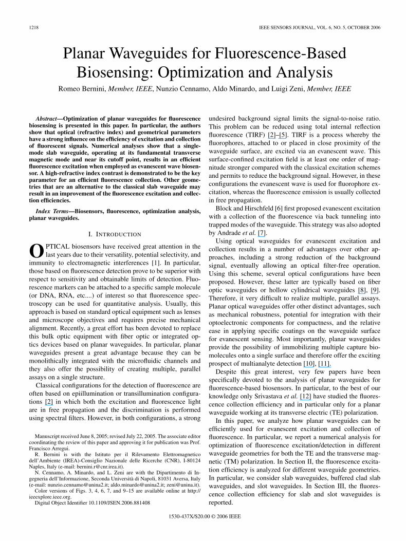
Fig. 1. Total internal reflection (TIR).
II. FLUORESCENCE EXCITATION EFFICIENCY
In optical waveguides, light confinement is usually basedon total internal reflection (TIR). When TIR occurs, a smallportion of the reflected light penetrates through the interface be-tween the guiding layer (with refractive index n2) and the covermedium (with refractive index n1) and propagates parallel tothe surface in the plane of incidence creating an electromagneticfield in the cover medium. The latter, named the evanescentfield, decays exponentially with increasing distance from theinterface (Fig. 1).
The evanescent field can be employed in a planar opticalwaveguide in both absorption and fluorescence sensors. Inabsorption-based sensors, the presence of an absorbing analytewithin the penetration depth of the evanescent field inducesan increase in the propagation loss of the propagating guidedmode(s). Such increase can be correlated with the concentrationof the analyte of interest.
In fluorescence-based biosensors, the evanescent field isemployed for the excitation of fluorophores residing in theimmediate region near the interface.
For both kinds of sensors, it is necessary to understand therole of the surrounding absorbing and/or fluorescent mediumon the sensor efficiency. In particular, it is useful to define asingle parameter, which quantifies the efficiency of evanescentfield-based sensors, independently of the particular waveguidegeometry adopted for the sensor. We define this parameter asthe ratio between the change in the absorption coefficient ofthe waveguide-guided mode and the change in the absorptioncoefficient of the cover medium where the biological probe ispresent. In fact, a change δεc of the dielectric constant of thecover medium results in a shift of the discrete eigenvalue [13]
β2 = β20 + δ(β2) (1)
where β0 is the unperturbed propagation constant of the modeof interest. For a particular bound mode in which the unper-turbed propagation constant β0 is real, the absorption coeffi-cient α produced by δεc is
α = Im{β} ∼= (2β0)−1Im{δ(β2)
}(2)
where Im stands for imaginary part. As changes in covermedium dielectric constant, due to either analyte absorptionor fluorescence excitation, are usually much smaller than theunperturbed value in evanescent field-based sensors, the calcu-lation of δ(β2) can be carried out by employing a first-orderperturbation approach [13], [14]. Perturbation technique hasthe advantage to permit the calculation of the waveguide mode
sensitivity to cover medium absorption changes, in any optoge-ometrical configurations. This is in contrast to other techniques,such as those based on the differentiation of the waveguidecharacteristic equation [15], where an analytical waveguidecharacteristic equation is needed for the specific wave-guide geometry.
According to the perturbation method, we can write for TEmodes [13]
δ(β2)TE = k20
+∞∫
−∞|Ey|2δε(x)dx
+∞∫
−∞|Ey|2dx
(3)
where k0 is the wavenumber in a vacuum, and Ey is the electricfield transverse component of the TE mode. The first-orderchange in the eigenvalue δ(β2) for TM modes can be calculatedas [13]
δ(β2)TM
=β2
0
+∞∫
−∞|Hy|2δε(x)/ε(x)2dx+
+∞∫
−∞|∂Hy/∂x|2δε(x)/ε(x)2dx
+∞∫
−∞|Hy|2/ε(x)dx
(4)
where Hy is the magnetic field transverse component of the TMmode. Our efficiency is then calculated as the ratio between theguided mode absorption coefficient α and the bulk absorptioncoefficient due to δεc(αc). Bulk absorption can be regarded asthe absorption of a plane wave and is given by
αc =k0Im(δεc)
2ncε0(5)
where nc is the unperturbed refractive index of the covermedium and ε0 is the vacuum permittivity.
Note that our efficiency is useful both for absorbance-basedand fluorescence-based sensors. In fact, for these latter theemitted power of fluorescence radiation Pf is proportionalto the total power absorbed by the fluorophores PAbs [16],that is
Pf = φPAbs (6)
where φ is the quantum efficiency, indicating the percentage ofabsorbed photons, which are converted into emitted fluorescentphotons. The absorption coefficient of the cover medium isrelated to the fluorophores concentration by
αc = εmolarC (7)
where εmolar is the molar extinction coefficient of the fluo-rophores at the excitation wavelength, and C is the fluorophoresmolar concentration. Once fixed the fluorophores concentra-tion (hence the absorption coefficient of the cover medium),the power absorbed by the fluorophores due to interactionwith the evanescent field of a guided mode depends on the
1220 IEEE SENSORS JOURNAL, VOL. 6, NO. 5, OCTOBER 2006
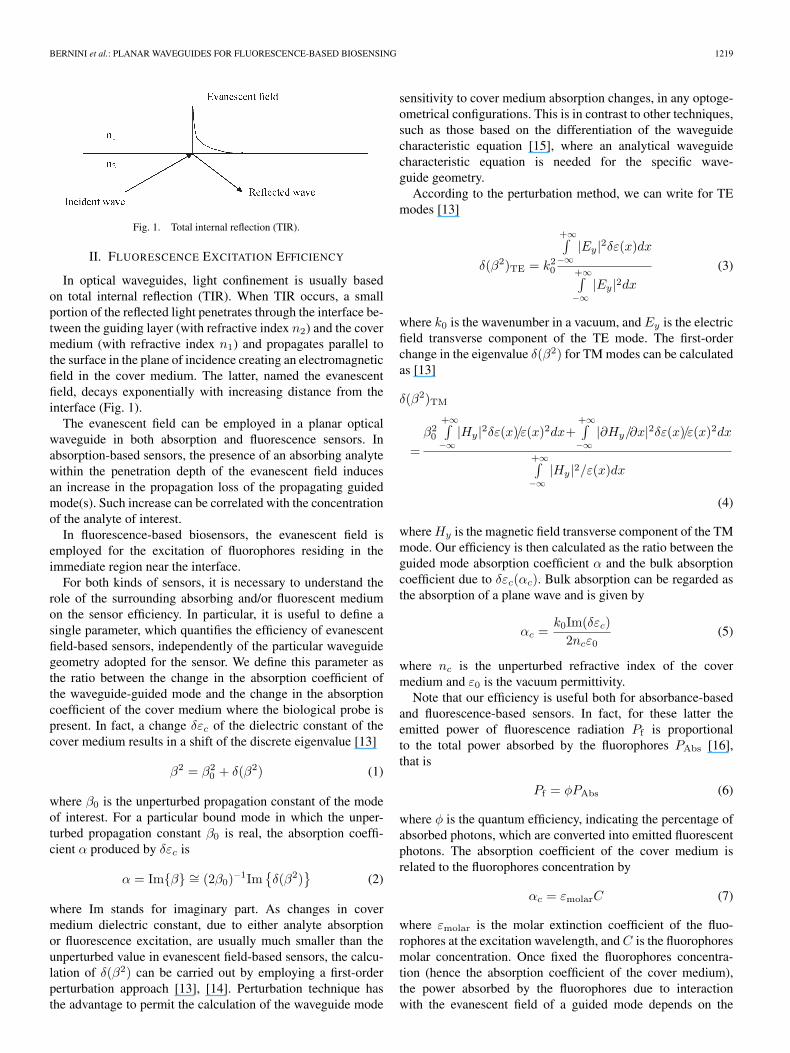
Fig. 2. Cross section of the slab planar waveguide sensor.
absorption coefficient of the mode itself [16]. Thus, efficiencyin fluorescence emission can be evaluated by using the samewaveguide efficiency parameter considered in our analysis, i.e.,by calculating the ratio between the waveguide mode absorp-tion coefficient and the cover medium absorption coefficient.This gives a measure of the power emitted by the fluorophores,for a given fluorophores concentration.
Numerical analyses have been carried out for three differ-ent monodimensional waveguide geometries: slab waveguide,buffered clad slab waveguide, and slot waveguides. For anygeometries, we will study the dependence of the sensor ef-ficiency on the optogeometrical parameters of the consideredstructure.
A. Slab Waveguides
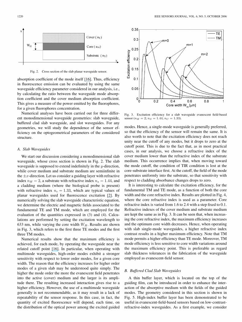
We start our discussion considering a monodimensional slabwaveguide, whose cross section is shown in Fig. 2. The slabwaveguide is supposed to extend indefinitely in the y-direction,while cover medium and substrate medium are semiinfinite inthe ±x-direction. Let us consider a guiding layer with refractiveindex nH = 2, a substrate with refractive index ns = 1.44, anda cladding medium (where the biological probe is present)with refractive index nc = 1.33, which are typical values ofplanar waveguides used for fluorescence excitation [2]. Bynumerically solving the slab waveguide characteristic equation,we determine the electric and magnetic fields associated to thefundamental TE and TM mode, which are employed for theevaluation of the quantities expressed in (3) and (4). Calcu-lations are performed by setting the excitation wavelength to633 nm, while varying the core width WH . Results are shownin Fig. 3, which refers to the first three TE modes and the firstthree TM modes.
Numerical results show that the maximum efficiency isachieved, for each mode, by operating the waveguide near therelated cutoff point [16]. In particular, when operating withmultimode waveguides, high-order modes exhibit a strongersensitivity with respect to lower order modes, for a given corewidth. The reason that the efficiency increases for higher ordermodes of a given slab may be understood quite simply. Thehigher the mode order the more the evanescent field penetratesinto the active (cover) medium and the larger is its ampli-tude there. The resulting increased interaction gives rise to ahigher efficiency. However, the use of a multimode waveguidegenerally is not recommendable, as it may result in a lack ofrepeatability of the sensor response. In this case, in fact, thequantity of excited fluorescence will depend, each time, onthe distribution of the optical power among the excited guided
Fig. 3. Excitation efficiency for a slab waveguide evanescent field-basedsensor (nH = 2; nS = 1.44; nC = 1.33).
modes. Hence, a single-mode waveguide is generally preferred,so that the efficiency of the sensor will remain the same. It isalso worth to note that the excitation efficiency does not reachunity near the cutoff of any modes, but it drops to zero at thecutoff point. This is due to the fact that, as in most practicalcases, in our analysis, we choose a refractive index of thecover medium lower than the refractive index of the substratemedium. This occurrence implies that, when moving towardthe mode cutoff, the condition of TIR condition is lost at thecore-substrate interface first. At the cutoff, the field of the modepenetrates uniformly into the substrate, so that sensitivity withrespect to cladding absorbance changes drops to zero.
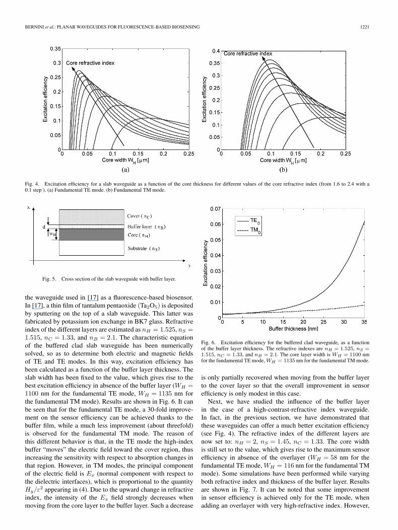
It is interesting to calculate the excitation efficiency, for thefundamental TM and TE mode, as a function of both the corewidth and the core refractive index. Results are plotted in Fig. 4,where the core refractive index is used as a parameter. Corerefractive index is varied from 1.6 to 2.4 with a step fixed to 0.1.Refractive indexes of the cover medium and substrate mediumare kept the same as in Fig. 3. It can be seen that, when increas-ing the core refractive index, the maximum efficiency increasesand the optimum core width decreases. Hence, when operatingwith slab single-mode waveguides, a higher refractive indexcontrast results in a higher maximum efficiency. Note that TMmode permits a higher efficiency than TE mode. Moreover, TMmode efficiency is less sensitive to core width variations aroundthe maximum efficiency point. This is preferable as regardslab thickness tolerances in the fabrication of the waveguideemployed as evanescent-field sensor.
B. Buffered Clad Slab Waveguides
A thin buffer layer, which is located on the top of theguiding film, can be introduced in order to enhance the inter-action of the absorptive medium with the fields of the guidedmodes. The geometry considered in this section is shown inFig. 5. High-index buffer layer has been demonstrated to beuseful in evanescent-field-based sensors based on low-contrast-refractive-index waveguides. As a first example, we consider
BERNINI et al.: PLANAR WAVEGUIDES FOR FLUORESCENCE-BASED BIOSENSING 1221
Fig. 4. Excitation efficiency for a slab waveguide as a function of the core thickness for different values of the core refractive index (from 1.6 to 2.4 with a0.1 step ). (a) Fundamental TE mode. (b) Fundamental TM mode.
Fig. 5. Cross section of the slab waveguide with buffer layer.
the waveguide used in [17] as a fluorescence-based biosensor.In [17], a thin film of tantalum pentaoxide (Ta2O5) is depositedby sputtering on the top of a slab waveguide. This latter wasfabricated by potassium ion exchange in BK7 glass. Refractiveindex of the different layers are estimated as nH = 1.525, nS =1.515, nC = 1.33, and nB = 2.1. The characteristic equationof the buffered clad slab waveguide has been numericallysolved, so as to determine both electric and magnetic fieldsof TE and TE modes. In this way, excitation efficiency hasbeen calculated as a function of the buffer layer thickness. Theslab width has been fixed to the value, which gives rise to thebest excitation efficiency in absence of the buffer layer (WH =1100 nm for the fundamental TE mode, WH = 1135 nm forthe fundamental TM mode). Results are shown in Fig. 6. It canbe seen that for the fundamental TE mode, a 30-fold improve-ment on the sensor efficiency can be achieved thanks to thebuffer film, while a much less improvement (about threefold)is observed for the fundamental TM mode. The reason ofthis different behavior is that, in the TE mode the high-indexbuffer “moves” the electric field toward the cover region, thusincreasing the sensitivity with respect to absorption changes inthat region. However, in TM modes, the principal componentof the electric field is Ex (normal component with respect tothe dielectric interfaces), which is proportional to the quantityHy/ε2 appearing in (4). Due to the upward change in refractiveindex, the intensity of the Ex field strongly decreases whenmoving from the core layer to the buffer layer. Such a decrease
Fig. 6. Excitation efficiency for the buffered clad waveguide, as a functionof the buffer layer thickness. The refractive indexes are nH = 1.525, nS =1.515, nC = 1.33, and nB = 2.1. The core layer width is WH = 1100 nmfor the fundamental TE mode, WH = 1135 nm for the fundamental TM mode.
is only partially recovered when moving from the buffer layerto the cover layer so that the overall improvement in sensorefficiency is only modest in this case.
Next, we have studied the influence of the buffer layerin the case of a high-contrast-refractive index waveguide.In fact, in the previous section, we have demonstrated thatthese waveguides can offer a much better excitation efficiency(see Fig. 4). The refractive index of the different layers arenow set to: nH = 2, nS = 1.45, nC = 1.33. The core widthis still set to the value, which gives rise to the maximum sensorefficiency in absence of the overlayer (WH = 58 nm for thefundamental TE mode, WH = 116 nm for the fundamental TMmode). Some simulations have been performed while varyingboth refractive index and thickness of the buffer layer. Resultsare shown in Fig. 7. It can be noted that some improvementin sensor efficiency is achieved only for the TE mode, whenadding an overlayer with very high-refractive index. However,
1222 IEEE SENSORS JOURNAL, VOL. 6, NO. 5, OCTOBER 2006
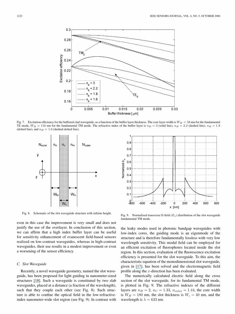
Fig. 7. Excitation efficiency for the buffered clad waveguide, as a function of the buffer layer thickness. The core layer width is WH = 58 nm for the fundamentalTE mode, WH = 116 nm for the fundamental TM mode. The refractive index of the buffer layer is nB = 3 (solid line), nB = 2.2 (dashed line), nB = 1.8(dotted line), and nB = 1.6 (dashed-dotted line).
Fig. 8. Schematic of the slot waveguide structure with infinite height.
even in this case the improvement is very small and does notjustify the use of the overlayer. In conclusion of this section,we can affirm that a high index buffer layer can be usefulfor sensitivity enhancement of evanescent field-based sensorsrealized on low-contrast waveguides, whereas in high-contrastwaveguides, their use results in a modest improvement or evena worsening of the sensor efficiency.
C. Slot Waveguide
Recently, a novel waveguide geometry, named the slot wave-guide, has been proposed for light guiding in nanometer-sizedstructures [18]. Such a waveguide is constituted by two slabwaveguides, placed at a distance (a fraction of the wavelength),such that they couple each other (see Fig. 8). Such struc-ture is able to confine the optical field in the low-refractive-index nanometer-wide slot region (see Fig. 9). In contrast with
Fig. 9. Normalized transverse E-field (Ex) distribution of the slot waveguidefundamental TM mode.
the leaky modes used in photonic bandgap waveguides withlow-index cores, the guiding mode is an eigenmode of thestructure and is therefore fundamentally lossless with very lowwavelength sensitivity. This modal field can be employed foran efficient excitation of fluorophores located inside the slotregion. In this section, evaluation of the fluorescence excitationefficiency is presented for the slot waveguide. To this aim, thecharacteristic equation of the monodimensional slot waveguide,given in [17], has been solved and the electromagnetic fieldprofile along the x-direction has been evaluated.
The numerically calculated electric field along the crosssection of the slot waveguide, for its fundamental TM mode,is plotted in Fig. 9. The refractive indexes of the differentlayers are nH = 2, nC = 1.33, nouter = 1.44, the core widthis WH = 180 nm, the slot thickness is Wc = 40 nm, and thewavelength is λ = 633 nm.
BERNINI et al.: PLANAR WAVEGUIDES FOR FLUORESCENCE-BASED BIOSENSING 1223
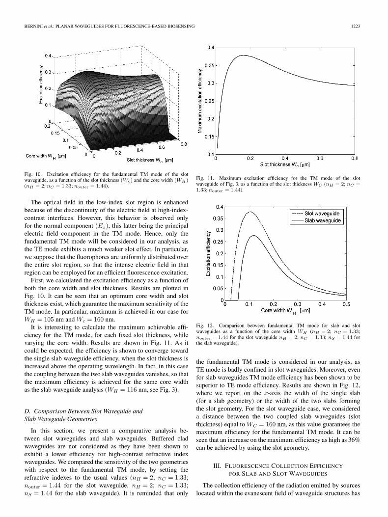
Fig. 10. Excitation efficiency for the fundamental TM mode of the slotwaveguide, as a function of the slot thickness (Wc) and the core width (WH)(nH = 2; nC = 1.33; nouter = 1.44).
The optical field in the low-index slot region is enhancedbecause of the discontinuity of the electric field at high-index-contrast interfaces. However, this behavior is observed onlyfor the normal component (Ex), this latter being the principalelectric field component in the TM mode. Hence, only thefundamental TM mode will be considered in our analysis, asthe TE mode exhibits a much weaker slot effect. In particular,we suppose that the fluorophores are uniformly distributed overthe entire slot region, so that the intense electric field in thatregion can be employed for an efficient fluorescence excitation.
First, we calculated the excitation efficiency as a function ofboth the core width and slot thickness. Results are plotted inFig. 10. It can be seen that an optimum core width and slotthickness exist, which guarantee the maximum sensitivity of theTM mode. In particular, maximum is achieved in our case forWH = 105 nm and Wc = 160 nm.
It is interesting to calculate the maximum achievable effi-ciency for the TM mode, for each fixed slot thickness, whilevarying the core width. Results are shown in Fig. 11. As itcould be expected, the efficiency is shown to converge towardthe single slab waveguide efficiency, when the slot thickness isincreased above the operating wavelength. In fact, in this casethe coupling between the two slab waveguides vanishes, so thatthe maximum efficiency is achieved for the same core widthas the slab waveguide analysis (WH = 116 nm, see Fig. 3).
D. Comparison Between Slot Waveguide andSlab Waveguide Geometries
In this section, we present a comparative analysis be-tween slot waveguides and slab waveguides. Buffered cladwaveguides are not considered as they have been shown toexhibit a lower efficiency for high-contrast refractive indexwaveguides. We compared the sensitivity of the two geometrieswith respect to the fundamental TM mode, by setting therefractive indexes to the usual values (nH = 2; nC = 1.33;nouter = 1.44 for the slot waveguide, nH = 2; nC = 1.33;nS = 1.44 for the slab waveguide). It is reminded that only
Fig. 11. Maximum excitation efficiency for the TM mode of the slotwaveguide of Fig. 3, as a function of the slot thickness WC (nH = 2; nC =1.33; nouter = 1.44).
Fig. 12. Comparison between fundamental TM mode for slab and slotwaveguides as a function of the core width WH (nH = 2; nC = 1.33;nouter = 1.44 for the slot waveguide nH = 2; nC = 1.33; nS = 1.44 forthe slab waveguide).
the fundamental TM mode is considered in our analysis, asTE mode is badly confined in slot waveguides. Moreover, evenfor slab waveguides TM mode efficiency has been shown to besuperior to TE mode efficiency. Results are shown in Fig. 12,where we report on the x-axis the width of the single slab(for a slab geometry) or the width of the two slabs formingthe slot geometry. For the slot waveguide case, we considereda distance between the two coupled slab waveguides (slotthickness) equal to WC = 160 nm, as this value guarantees themaximum efficiency for the fundamental TM mode. It can beseen that an increase on the maximum efficiency as high as 36%can be achieved by using the slot geometry.
III. FLUORESCENCE COLLECTION EFFICIENCY
FOR SLAB AND SLOT WAVEGUIDES
The collection efficiency of the radiation emitted by sourceslocated within the evanescent field of waveguide structures has
1224 IEEE SENSORS JOURNAL, VOL. 6, NO. 5, OCTOBER 2006
been studied in different papers [12], [19]. Collection efficiencyby means of a light guiding structure can be calculated by sum-ming over the collection efficiency of each mode (TE or TM)supported by the waveguide. By modeling the fluorophores aselementary dipoles, collection efficiency of each single modecan be evaluated as the ratio between the integral of the squaredelectric field, related to the mode of interest, over the regionoccupied by the fluorophores, and the total power P0 carried bythe mode itself [19], that is
(collection efficiency)ν =
∫
V
S| �Eν |2
P0(8)
where S indicates the source strength, and �Eν is the elec-tric field related to the mode of index ν. The volume inte-gral extends over the region V occupied by the fluorophores.The subscript ν refers to the modal index. By supposing arandom orientation of the elementary dipoles (fluorophores),any components of the electric field have to be included inthe calculation of the integral of (8). In the following, weshall compare slab and slot geometries as regard fluorescencecollection efficiency. For the slab geometry, we suppose firstthat the fluorescence layer extends enough to ensure that theevanescent field tails of the modes have decayed to insignificantvalues. In this hypothesis, the squared electric field in (8) canbe numerically integrated over the whole cover region. Analo-gously, for slot waveguides, we suppose a uniform distributionof the fluorophores within the slot region, so that the volume Vcoincides with the slot region. The wavelength for fluorescencecollection analysis is set to 690 nm.
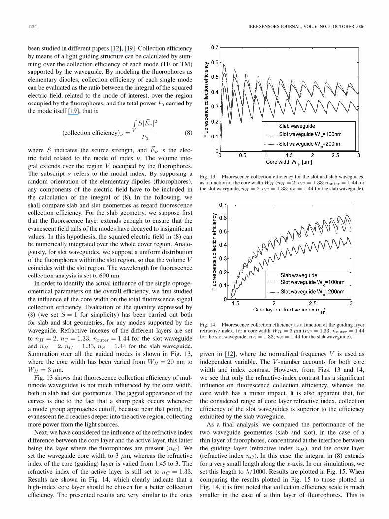
In order to identify the actual influence of the single optoge-ometrical parameters on the overall efficiency, we first studiedthe influence of the core width on the total fluorescence signalcollection efficiency. Evaluation of the quantity expressed by(8) (we set S = 1 for simplicity) has been carried out bothfor slab and slot geometries, for any modes supported by thewaveguide. Refractive indexes of the different layers are setto nH = 2, nC = 1.33, nouter = 1.44 for the slot waveguideand nH = 2, nC = 1.33, nS = 1.44 for the slab waveguide.Summation over all the guided modes is shown in Fig. 13,where the core width has been varied from WH = 20 nm toWH = 3 µm.
Fig. 13 shows that fluorescence collection efficiency of mul-timode waveguides is not much influenced by the core width,both in slab and slot geometries. The jagged appearance of thecurves is due to the fact that a sharp peak occurs whenevera mode group approaches cutoff, because near that point, theevanescent field reaches deeper into the active region, collectingmore power from the light sources.
Next, we have considered the influence of the refractive indexdifference between the core layer and the active layer, this latterbeing the layer where the fluorophores are present (nC). Weset the waveguide core width to 3 µm, whereas the refractiveindex of the core (guiding) layer is varied from 1.45 to 3. Therefractive index of the active layer is still set to nC = 1.33.Results are shown in Fig. 14, which clearly indicate that ahigh-index core layer should be chosen for a better collectionefficiency. The presented results are very similar to the ones
Fig. 13. Fluorescence collection efficiency for the slot and slab waveguides,as a function of the core width WH (nH = 2; nC = 1.33; nouter = 1.44 forthe slot waveguide, nH = 2; nC = 1.33; nS = 1.44 for the slab waveguide).
Fig. 14. Fluorescence collection efficiency as a function of the guiding layerrefractive index, for a core width WH = 3 µm (nC = 1.33; nouter = 1.44for the slot waveguide, nC = 1.33; nS = 1.44 for the slab waveguide).
given in [12], where the normalized frequency V is used asindependent variable. The V -number accounts for both corewidth and index contrast. However, from Figs. 13 and 14,we see that only the refractive-index contrast has a significantinfluence on fluorescence collection efficiency, whereas thecore width has a minor impact. It is also apparent that, forthe considered range of core layer refractive index, collectionefficiency of the slot waveguides is superior to the efficiencyexhibited by the slab waveguide.
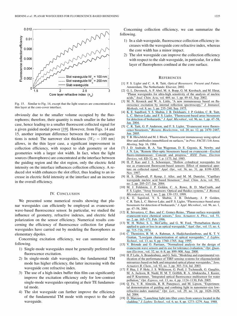
As a final analysis, we compared the performance of thetwo waveguide geometries (slab and slot), in the case of athin layer of fuorophores, concentrated at the interface betweenthe guiding layer (refractive index nH ), and the cover layer(refractive index nC). In this case, the integral in (8) extendsfor a very small length along the x-axis. In our simulations, weset this length to λ/1000. Results are plotted in Fig. 15. Whencomparing the results plotted in Fig. 15 to those plotted inFig. 14, it is first noted that collection efficiency scale is muchsmaller in the case of a thin layer of fluorophores. This is
BERNINI et al.: PLANAR WAVEGUIDES FOR FLUORESCENCE-BASED BIOSENSING 1225
Fig. 15. Similar to Fig. 14, except that the light sources are concentrated in athin layer at the core-cover interface.
obviously due to the smaller volume occupied by the fluo-rophores; therefore, their quantity is much smaller in the lattercase, hence leading to a smaller fluorescent collected signal fora given guided modal power [19]. However, from Figs. 14 and15, another important difference between the two configura-tions is noted: The narrower slot thickness (WC = 100 nm)allows, in the thin layer case, a significant improvement incollection efficiency, with respect to slab geometry or slotgeometries with a larger slot width. In fact, when the lightsources (fluorophores) are concentrated at the interface betweenthe guiding region and the slot region, only the electric fieldintensity on the interface influences collection efficiency. A re-duced slot width enhances the slot effect, thus leading to an in-crease in electric field intensity at the interface and an increasein the overall efficiency.
IV. CONCLUSION
We presented some numerical results showing that pla-nar waveguides can efficiently be employed as evanescent-wave-based fluorescence sensor. In particular, we studied theinfluence of geometry, refractive indexes, and electric fieldpolarization on the sensor efficiency. Numerical results con-cerning the efficiency of fluorescence collection for planarwaveguides have carried out by modeling the fluorophores aselementary dipoles.
Concerning excitation efficiency, we can summarize thefollowing.
1) Single-mode waveguides must be generally preferred forfluorescence excitation.
2) In single-mode slab waveguides, the fundamental TMmode has higher efficiency, the latter increasing with thewaveguide core refractive index.
3) The use of a high-index buffer thin film can significantlyimprove the excitation efficiency only for low-contrastsingle-mode waveguides operating at their TE fundamen-tal mode.
4) The slot waveguide can further improve the efficiencyof the fundamental TM mode with respect to the slabwaveguide.
Concerning collection efficiency, we can summarize thefollowing.
1) In a slab waveguide, fluorescence collection efficiency in-creases with the waveguide core refractive index, whereasthe core width has a minor impact.
2) The slot waveguide can improve the collection efficiencywith respect to the slab waveguide, in particular, for a thinlayer of fluorophores confined at the core surface.
REFERENCES
[1] F. S. Ligler and C. A. R. Taitt, Optical Biosensors: Present and Future.Amsterdam, The Netherlands: Elsevier, 2002.
[2] G. L. Duveneck, A. P. Abel, M. A. Bopp, G. M. Kresbach, and M. Ehrat,“Planar waveguides for ultra-high sensitivity of the analysis of nucleicacids,” Anal. Chim. Acta, vol. 469, no. 1, pp. 49–61, Sep. 2002.
[3] M. N. Kronick and W. A. Little, “A new immunoassay based on flu-orescence excitation by internal reflection spectroscopy,” J. Immunol.Methods, vol. 8, no. 3, pp. 235–240, Sep. 1975.
[4] K. E. Sapdford, Y. S. Shubin, J. B. Delehanty, J. P. Golden, C. R. Taitt,L. C. Shriver-Lake, and F. S. Ligler, “Fluorescent-based array biosensorsfor detection of biohazards,” J. Appl. Microbiol., vol. 96, no. 1, pp. 47–58,Jan. 2004.
[5] C. R. Taitt, G. P. Anderson, and F. S. Ligler, “Evanescent wave fluores-cence biosensors,” Biosens. Bioelectron., vol. 20, no. 12, pp. 2470–2487,Jun. 2005.
[6] T. B. Hirschfeld and M. J. Block, “Fluorescent immunoassay using opticalfiber and antibodies immobilized on surfaces,” in Proc. FACSS 11th Annu.Meeting, Sep. 16, 1984.
[7] J. D. Andrade, R. A. Van Wageman, D. E. Grgonis, K. Newby, andJ. N. Lin, “Remote fiber-optic biosensors based on evanescent—Excitedfluoro-immunoassay: Concept and progress,” IEEE Trans. ElectronDevices, vol. ED-32, no. 7, p. 1175, Jul. 1985.
[8] H. P. Kao and J. S. Schoeniger, “Hollow cylindrical waveguides foruse as evanescent fluorescent-based sensors: Effect of numerical aper-ture on collected signal,” Appl. Opt., vol. 36, no. 31, pp. 8199–8205,Nov. 1997.
[9] H. S. Dhadwall, P. Kemp, J. Aller, and M. M. Dantzler, “Capillarywaveguide nucleic acid based biosensor,” Anal. Chim. Acta, vol. 501,no. 2, pp. 205–217, Jan. 2004.
[10] M. J. Feldstein, J. P. Golden, C. A. Rowe, B. D. MacCraith, andF. S. Ligler, “Array biosensors: Optical and fluidics systems,” J. Biomed.Microdevices, vol. 1, no. 2, pp. 139–153, 1999.
[11] K. E. Sapsford, Y. S. Shubin, J. B. Delehanty, J. P. Golden,C. R. Taitt, L. C. Shriver-Lake, and F. S. Ligler, “Fluorescence-based arraybiosensors for detection of biohazards,” J. Appl. Microbiol., vol. 96, no. 1,pp. 47–58, 2004.
[12] R. Srivastava, C. Bao, and C. Gomez-Reino, “Planar-surface-waveguideevanescent-wave chemical sensors,” Sens. Actuators A, Phys., vol. 51,no. 2, pp. 165–171, Feb. 1996.
[13] W. H. Weber, S. L. McCarthy, and G. W. Ford, “Perturbation theoryapplied to gain or loss in an optical waveguide,” Appl. Opt., vol. 13, no. 4,pp. 715–716, 1974.
[14] C. Themistos, B. M. A. Rahman, A. Hadjicharalambous, and K. T. V.Grattan, “Loss/gain characterization of optical waveguides,” J. Lightw.Technol., vol. 13, no. 8, pp. 1760–1765, Aug. 1995.
[15] V. Brioude and O. Parriaux, “Normalized analysis for the design ofevanescent-wave sensors and its use for tolerance evaluation,” Opt. Quan-tum Electron., vol. 32, no. 6–8, pp. 899–908, Aug. 2000.
[16] H. P. Lehr, A. Brandenburg, and G. Sulz, “Modeling and experimental ver-ification of the performance of TIRF-sensing systems for oligonucleotidemiroarrays based on bulk and integrated optical planar waveguides,” Sens.Actuators B, Chem., vol. 92, no. 3, pp. 303–314, Jul. 2003.
[17] P. Hua, J. P. Hole, J. S. Wilkinson, G. Proll, J. Tschmealk, G. Gauglitz,M. A. Jackson, R. Nudd, H. M. T. Griffith, R. A. Abuknesha, J. Kasier,and P. Kraemmer, “Integrated optical fluorescence multisensor for waterpollution,” Opt. Express, vol. 13, no. 4, pp. 1124–1130, Feb. 2005.
[18] Q. Fu, V. R. Almeida, R. R. Panepucci, and M. Lipson, “Experimen-tal demonstration of guiding and confining light in nanometer-size low-refractive-index material,” Opt. Lett., vol. 29, no. 14, pp. 1626–1628,Jul. 2004.
[19] D. Marcuse, “Launching light into fiber cores from sources located in thecladding,” J. Lightw. Technol., vol. 6, no. 8, pp. 1273–1279, Aug. 1988.
1226 IEEE SENSORS JOURNAL, VOL. 6, NO. 5, OCTOBER 2006
Romeo Bernini (M’01) was born in Italy in 1968.He received the degree (summa cum laude) from theUniversity of Naples Federico II, Naples, Italy, in1995 and the Ph.D. degree from Second Universityof Naples in 1999, both in electronic engineering.
In 1999, he worked at Delft Institute of Microelec-tronics and Submicrontechnology (DIMES), Tech-nical University of Delft, Delft, The Netherlands.During 2000, he was Research Fellow at the SecondUniversity of Naples. He is currently a ResearchScientist at the “Istituto per il Rilevamento Elettro-
magnetico dell’Ambiente” (IREA) of the National Research Council of Italy.His main fields of interest include optoelectronic sensors and devices, fibersensors and nondestructive characterization of semiconductor, and dielectricmaterials.
Nunzio Cennamo was born in Italy in 1975. Hereceived the degree in electronic engineering fromthe Second University of Naples, Naples, Italy, in2002, where he is currently working toward the Ph.D.degree in electronic engineering.
His research activity deals with integrated opticssensors and optoelectronic devices.
Aldo Minardo was born in Italy in 1974. He re-ceived the degree (summa cum laude) from Univer-sity of Naples Federico II, Naples, Italy, in 2000 andthe Ph.D. degree from Second University of Naplesin 2003, both in electronic engineering.
His research activity deals with distributed opticalfiber sensors and optoelectronic devices.
Luigi Zeni (M’98) was born in Italy in 1962. Hereceived the degree in electronic engineering (summacum laude) from University of Naples, Naples, Italy,in 1988 and the Ph.D. degree in electronics and com-puter science from Italian Ministry of University,Rome, Italy, and Scientific Research, in 1992.
From 1993 to 1998, he was an Assistant Professorat the University of Naples “Federico II.” In 1994,he was with DIMES, Technical University of Delft,Delft, The Netherlands, as a Visiting Scientist. Since1998, he has been an Associate Professor of Elec-
tronics at the Second University of Naples. His teaching activity includesanalog/digital electronics and optoelectronics. He has been a Coordinator ofresearch projects financed by the Italian Ministry of University and ScientificResearch. He serves as referee for international journals and has publishedmore than 50 papers in international journals and more than 60 papers in theproceedings of international conferences. He also serves as a Reviewer forresearch projects of the Italian Ministry of University and Scientific Researchand the European Union. His research fields are optoelectronic devices andsensors, materials characterization for microelectronics and optoelectronics,wideband contactless techniques for electronic circuits characterization, andlaser beam characterization.
Dr. Zeni is a member of the Associated Electrical Industries (AEI).