
Semianalytical method to study silicon slot waveguides for optical sensing application
8
Semianalytical method to study silicon slot waveguides for optical sensing application Saikat Majumder Rajib Chakraborty
Transcript of Semianalytical method to study silicon slot waveguides for optical sensing application

Semianalytical method to study siliconslot waveguides for optical sensingapplication
Saikat MajumderRajib Chakraborty

Semianalytical method to study silicon slot waveguidesfor optical sensing application
Saikat Majumder *
Rajib ChakrabortyUniversity of CalcuttaDepartment of Applied Optics and PhotonicsKolkata 700 009, IndiaE-mail: [email protected]
Abstract. High-index contrast slab and slot optical waveguides have ahigh index variation both along the lateral and vertical interfaces andare usually analyzed numerically, requiring large computer memory andtime. In this article, their analysis is done semianalytically using an effec-tive-index based matrix method. This method, which is computationallyvery fast, was earlier used successfully for low-index profile waveguidestructures only and is now suitably modified for use in high-index contraststructures. The electric field profile of the waveguide structures is plottedand the effective refractive index at different wavelengths is calculated.The results are compared with results obtained from numerical techniqueslike finite element method, finite-difference time-domain, and beam propa-gation method and they match very well. The dependence of their differentoptical characteristics with the waveguide parameters is also studied.These studies will help in obtaining improved sensitivity of slot waveguidesfor sensing applications. © 2013 Society of Photo-Optical Instrumentation Engineers(SPIE) [DOI: 10.1117/1.OE.52.10.107102]
Subject terms: slot waveguide; high-index contrast; effective index; matrix method;sensors.
Paper 130793 received May 31, 2013; revised manuscript received Sep. 2, 2013;accepted for publication Sep. 4, 2013; published online Oct. 3, 2013.
1 IntroductionToday’s demand for increased performance in terms ofhigher interconnect density and bandwidth in telecommuni-cation has resulted in photonic integrated devices made ofwaveguides, which must satisfy large-scale integration,device miniaturization, implementation of system-on-chiparchitectures, and ultimately, cost reduction. For its imple-mentation, tight light confinement using high-contrastwaveguides is required which will form the platform forultra-compact photonic devices. Such high-contrast opticalwaveguide-based devices can be fabricated on commerciallyavailable silicon-on-insulator (SOI) wafers. These wafersconsist of three layers: the Si substrate, followed by a silica(SiO2) buffer, and a crystalline Si layer on the top. The wave-guide formed can be denoted as a high-contrast slab wave-guide or photonic wire. Vertical confinement of light isobtained from the index contrast between the silicon coreand the low index cladding and the buried silicon dioxidelayer, whereas lateral confinement can be obtained by litho-graphically patterning the silicon. Advances in the siliconfabrication process have enabled realization of ultra-smalldimension optical waveguide devices, too. However, whenthis dimension decreases to the wavelength of the incidentlight, even the high index ratio between silicon and silicacannot realize a good confinement of the optical field.Also at very high optical intensities, two-photon absorptionin the silicon may lead to high optical losses. Moreover, newfunctionalities like electro-optic modulation or chemicalsensing with optically active cladding requires maximizationof field intensity overlap between the optical waveguide
mode and a lower index cladding material. A slot waveguidestructure first proposed by Almeida et al.1 can concentrate alarge fraction of the guided mode of optical waveguides intoa nanometer scale low-index layer between two high-indexstrips. They can, therefore, be a useful tool for achievingenhanced field intensity, large field overlap with claddingmaterial, strong light matter interaction due to subwave-length dimension and low effective index.
The high contrast slab waveguides provide a high electricfield to invoke a nonlinear effect and a number of deviceslike Raman laser,2 wavelength converter,3 signal regenera-tor,4 and logic gates5 are fabricated on them. Slot waveguidesare now becoming very popular for applications likesensing,6–9 nano-optomechanics,10,11 nonlinear effects,12–17
optical modulation,15–17 and optical manipulation.18–20 So,analysis of its wave equation to determine its essentialparameters, such as propagation constant, field profile,and field confinement, is required for designing these wave-guide-based devices. The solution of the wave equation forthese types of waveguides is usually done numerically byfinite difference method, finite element method, or beampropagation method. The finite element or finite differencemethods basically discretize the transverse domain of anoptical waveguide to induce an eigenvalue problem.Commercial software using these numerical methods isalready available in the market. However, these methodstake a lot of computation time as well as memory. The semi-analytical methods, although not as accurate as numericalmethods, can be an alternative approach for evaluation ofthe waveguide parameters where the time and computermemory requirement is significantly less. Matrix methodis one such semianalytical method, which was first usedby Ghatak et al. for determination of propagation constantof planar waveguide.21 He extended it for quantum well
*Present address: Department of AE and I, Techno India, Kolkata 700091,India
0091-3286/2013/$25.00 © 2013 SPIE
Optical Engineering 107102-1 October 2013/Vol. 52(10)
Optical Engineering 52(10), 107102 (October 2013)

structure,22 determination of bending loss of waveguide,23
and numerical analysis of optical fiber.24 The method con-siders the given structure as a stratified medium and thenuses straightforward multiplication of 2 × 2 transfer matri-ces. Later, the corresponding author and his coworkers com-bined the effective index method with the matrix formulationto determine the propagation constant, field profile, andbending loss of diffused waveguides formed by titaniumindiffusion in LiNbO3.
25 This method has been termed asan effective-index based matrix method (EIMM) and hasalso been used to study electro-optic switches and periodi-cally segmented waveguides.26,27
In this article, it is shown that EIMM can be successfullyapplied for determining thewaveguide parameters of the high-index contrast slot waveguides for its use in sensing applica-tion. For the sake of completeness, the study starts with theanalysis of high-contrast slab waveguides and thenextends to slot waveguides. The issue for high-index contrastwaveguides is that thewaves suffer a discontinuity at the inter-face of two high-contrast mediums. For quasi-transverse elec-tric (TE)mode and quasi-transversemagnetic (TM)mode, thenormal component of electric field is perpendicular to the ver-tical walls and horizontal walls, respectively, where theyundergo strong discontinuity. As such the EIMM, whichcan be easily applied for slowly varying refractive index pro-files or low contrast waveguides, needs to be suitably modi-fied in these cases. For bend slot waveguides, analyticalsolutions using Bessel–Hankel function28 or semianalyticalsolution using effective-index method and Airy function29
exist. For straight slot waveguides, the proposed methodusing 2 × 2 transfer matrix is an even simpler option, notrequiring any function. The use of functions may introduceadditional approximation in calculation if all orders of anyfunction are not considered. The proposed method can beapplied to bend slot waveguides, too. However, sensors pro-posed with bend slot waveguides that are analyzed using Airyfunction as in Ref. 30 will always have an unnecessary bend-ing loss component in comparison to straight slot waveguidesensors, and to compensate that asymmetry in waveguidestructure is required.
2 Wave Propagation in a High-Contrast WaveguideFigure 1(a) shows a slot waveguide, which can concentrate alarge fraction of the guided mode of optical waveguides intoa nanometer scale low-index layer between two high-indexslab waveguides. If the cross-section of the entire structure isdivided into a multilayered structure [Fig. 1(b)] having “N”equal layers, then as derived in Ref. 21, the electric field ofthe light ray incident at an angle θi at any one layer (say i’thlayer) can be written as
~Ei ¼ ~uþi Eþi e
jΔi exp½jðωt − Ki cos θix − βzÞ�þ ~u−i E
−i e
−jΔi exp½jðωtþ Ki cos θix − βzÞ�; (1)
where Δ1 ¼ Δ2 ¼ 0; Δ3 ¼ K3d2 cos θ3; Δ3 ¼K4 cos θ4ðd2 þ d3Þ; Δi ¼ Ki cos θiðd2 þ d3 þ : : : þ di−1Þ;Ki ¼ K0ni ¼ ω
c ni.E�i and u�i are the magnitudes and the unit vectors,
respectively, along the electric field vectors associatedwith the downward and upward propagating waves, respec-tively. Ki is the wave constant.
E�i and E�
N are interrelated in matrix form as
�Eþi
E−i
�¼ SiN
�EþN
E−N
�; (2)
where SiN ¼ SiSiþ1: : : SN−1 ¼Q
N−1i Si,
Si ¼1
Ti
�expðjδiÞ Ri expðjδiÞRi expð−jδiÞ expð−jδiÞ
�;
δi ¼ Kidi cos θi: (3)
But at the interface of two media having high-index con-trast, the boundary condition will be that the normal compo-nents of electric displacement vector are continuous, whereasthe electric field is discontinuous. The tangential componentof the magnetic field will be continuous but then magneticdensity/magnetic induction will be discontinuous. But forlow-index contrast, both the electric and magnetic fieldare continuous. The transmission (Ti) and reflection coeffi-cient (Ri) at the interface of high-index contrast waveguidestructures will be given by
Fig. 1 (a) A typical slot waveguide structure consisting of low indexslot (r:i: ¼ ns and width ¼ Ws) between two high index slab wave-guides (r:i: ¼ nh , width ¼ Wh , thickness ¼ h). nc represent claddingr.i. (b) Propagation of light through a multilayered structure.
Optical Engineering 107102-2 October 2013/Vol. 52(10)
Majumder and Chakraborty: Semianalytical method to study silicon slot waveguides for optical sensing application
Ti ¼ 2n2i cos θin2i cos θi þ n2iþ1 cos θiþ1
; (4)
Ri ¼ n2i cos θi − n2iþ1 cos θiþ1
n2i cos θi þ n2iþ1 cos θiþ1
; (5)
for TE mode and
Ti ¼ 2n2i cos θin2i cos θiþ1 þ n2iþ1 cos θi
; (6)
Ri ¼ n2i cos θiþ1 − n2iþ1 cos θin2i cos θiþ1 þ n2iþ1 cos θi
; (7)
for TM mode.For two adjacent layers within the medium of same refrac-
tive index, the value of transmission and reflection coeffi-cients obtained using Eqs. (4)–(7) is same as that given inRef. 21. Only at high-contrast interface, the coefficientsgiven in Ref. 21 are approximated by the above set of equa-tions in this analysis because the electric field encounters anappreciable amount of discontinuity at the high-contrastinterface, and the amount of discontinuity is comparableto the square of the index ratio at the interface as reportedin Ref. 31. Therefore, Eqs. (4)–(7) can be used here to re-present the transmission and reflection coefficients of allthe layer interfaces. Thus, for high-index contrast waveguidestructures, the reflection and transmission coefficients cannow be assumed to be related to square of the refractiveindex, unlike that of low-index contrast structures whosecoefficients are given in Ref. 21. It is to be noted thatEqs. (4)–(7) are heuristic and that their use is empiricallyproposed here for studying quasi TE/TM modes with highdielectric contrast. This has been justified from the compa-rable results obtained from the proposed numerical simula-tions with other numerical techniques as given in the nextsection. Assuming that there is no backward propagatingwave from the last (i.e., N’th) layer, the forward and back-ward propagating wave in each layer can easily be found outfrom which the effective index or the field profile for thestructure can easily be obtained.
The high-contrast slab waveguides have a refractive indexvariation both along the horizontal and vertical directions. Asits dimension along the direction of propagation (i.e., alongz-axis) is infinitely large compared to other two (i.e., x- andy-axis), it may be considered as a two-dimensional (2-D)waveguide. So, the 2-D variation of refractive indexnðx; yÞ at any x is to be replaced by a one-dimensional(1-D) effective refractive index nðxÞ along the lateral direc-tion in order to use the above set of equations. In order to dothat, if quasi-TE modes are considered along the lateraldirection, the propagation constant of quasi-TM modesalong the vertical direction is found out using the matrixmethod given in Ref. 21. From the propagation constant,the effective refractive index is found out. Thus, usingthis technique, it is possible to find the effective refractiveindex of the slab waveguide with variation only along thelateral direction from the refractive index profile, whichhave variation both along the lateral and vertical directions.
To get the 1-D effective refractive index profile of the slotwaveguide, the 2-D profile of the slab region is replacedby its 1-D effective index profile. Thus, the 2-D refractiveindex profile of both slab and slot waveguide can be con-verted to their corresponding 1-D effective index profile.Now, the different parameters of the structure can easilybe obtained from the 1-D profile using the above set ofequations.
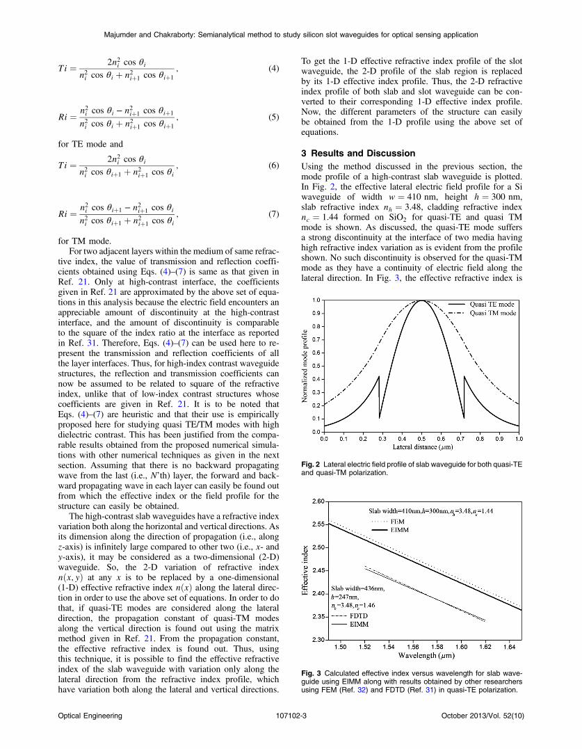
3 Results and DiscussionUsing the method discussed in the previous section, themode profile of a high-contrast slab waveguide is plotted.In Fig. 2, the effective lateral electric field profile for a Siwaveguide of width w ¼ 410 nm, height h ¼ 300 nm,slab refractive index nh ¼ 3.48, cladding refractive indexnc ¼ 1.44 formed on SiO2 for quasi-TE and quasi TMmode is shown. As discussed, the quasi-TE mode suffersa strong discontinuity at the interface of two media havinghigh refractive index variation as is evident from the profileshown. No such discontinuity is observed for the quasi-TMmode as they have a continuity of electric field along thelateral direction. In Fig. 3, the effective refractive index is
Fig. 2 Lateral electric field profile of slab waveguide for both quasi-TEand quasi-TM polarization.
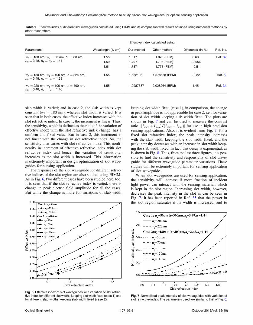
Fig. 3 Calculated effective index versus wavelength for slab wave-guide using EIMM along with results obtained by other researchersusing FEM (Ref. 32) and FDTD (Ref. 31) in quasi-TE polarization.
Optical Engineering 107102-3 October 2013/Vol. 52(10)
Majumder and Chakraborty: Semianalytical method to study silicon slot waveguides for optical sensing application

plotted versus wavelength for slab waveguide. For a slabwaveguide of width w ¼ 410 nm, it is seen that the resultscalculated using the proposed method matches very wellwith the theoretical results obtained using the finite elementmethod (FEM).32 The finite-difference time-domain (FDTD)simulation values for different wavelengths for a waveguidehaving dimensions w ¼ 436 nm, h ¼ 247 nm, nh ¼ 3.48,and nc ¼ 1.46 given in Ref. 31 are also compared withthe results obtained using the matrix method. As is evidentfrom the graph, the two results match very well. Thus, it canbe concluded that EIMM applied to high-contrast wave-guides gives similar results as that calculated with othersophisticated numerical techniques.
Next, the high-index contrast slot waveguide, as shown inFig. 1(a), is considered. It consists of two single-mode Sislab waveguides (nslab ¼ nh ¼ 3.48) each having widthðwhÞ ¼ 180 nm and separated by a slot (nslot ¼ns ¼ 1.44) of width ðwsÞ ¼ 50 nm formed on SOI platform.The dimension of the slot is comparable to the exponentialdecay length of the fundamental mode of the slab waveguide.As each slab has a 2-D variation of refractive indexnslabðx; yÞ, they are first converted into effective 1-D refrac-tive index similar to the process described before for the slabwaveguide. For a wavelength of 1.55 μm, this effectiverefractive index comes out to be nslabðxÞ ¼ 3.054. Thus,the structure is now converted into a three-layered planarstructure with refractive index nslabðxÞ, nslot, and nslabðxÞ.The electric field profile for the structure can now be easilyobtained using the matrix approach and is shown in Fig. 4 forthe quasi-TE mode. The electric field profile is perfectlysymmetric with an extremely high peak in the slot region,Gaussian distribution at the slab (high index) region (bothsides), and exponential decay in low index cladding region(both sides). This is exactly the same as the electric field pro-file of Ref. 1 whose dimensions are considered here. Thestructure, however, supports two waveguide modes withthe fundamental mode at β ¼ 7.36388277. The amplitudefor the asymmetric mode (second-order mode) is verysmall compared to the fundamental mode and is thereforenot shown here. The high-light confinement in the lowindex slot region is a function of discontinuity, which isrelated to the ratio of refractive index between the two
media.33 The enhancement of the electric field in the slotregion in comparison to the slab region is similar to the con-finement factor, as is evident in Fig. 4.
Now, if the slot thickness is varied, the propagation con-stant (or effective refractive index) of the entire structure alsochanges. For quasi-TE polarization, the effective refractiveindex of the structure is plotted for different slot thicknessesand is shown in Fig. 5. For no slot condition, the effectiverefractive index, neff (i.e., β∕K), is maximum which is 2.312at 1.55 μm for the waveguide dimension given in Ref. 1.When the slot is introduced between two slabs, even for aslot of 10 nm, a strong decrease of neff from 2.312 to2.098 occurs. As most of the fields will concentrate in thelow index slot region, the decrement in effective refractiveindex occurs. However, if the slot thickness is increased fur-ther, the effective refractive index also decreases till the slotthickness approaches the limit of decay length of the funda-mental mode of the slab waveguide. But the rate of decre-ment is not linear. From the plot of effective refractiveindex with slot thicknesses it is seen that it follows an expo-nential decay curve.
The results obtained for slot waveguides using the pro-posed method are also compared with the results obtainedby other researchers using the numerical method likeFEM and beam propagation method (BPM). In Table 1,the effective refractive index of slot waveguide structurewith three different waveguide parameters calculated usingEIMM for different wavelengths is given. They are com-pared with the results obtained using numerical methodslike FEM (Refs. 6 and 32) and BPM.34 As is revealedfrom the data, the results obtained with the proposed methodand FEM numerical method are almost the same (maximumdifference is 0.6%) while the difference with BPM isonly 1.45%.
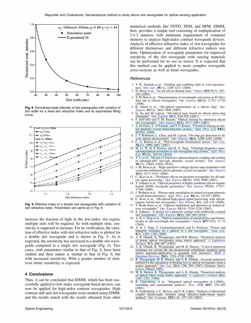
In Fig. 6, the variation of the effective index with therefractive index of the slot is plotted. This can occurwhen the slot is filled with different materials and so thisresult will give an idea about the sensitivity of the structureto different materials. Taking the same waveguide materials(nh ¼ 3.48, nc ¼ 1.44), two different cases are studied. Incase 1, slot width is kept constant (ws ¼ 50 nm), whereas
Fig. 4 Lateral electric field profile of slot waveguide for quasi-TEpolarization.
Fig. 5 Simulation results of the effective index of the slot waveguide fordifferent slot widths using EIMM along with its exponential fitting curve.
Optical Engineering 107102-4 October 2013/Vol. 52(10)
Majumder and Chakraborty: Semianalytical method to study silicon slot waveguides for optical sensing application
slab width is varied; and in case 2, the slab width is keptconstant (wh ¼ 180 nm), whereas slot width is varied. It isseen that in both cases, the effective index increases with theslot refractive index. In case 1, the increment is linear. Thus,the sensitivity, which is defined as the ratio of the variation ofeffective index with the slot refractive index change, has auniform and fixed value. But in case 2, this increment isnot linear with the change in slot refractive index. So, thesensitivity also varies with slot refractive index. This nonli-nearity in increment of effective refractive index with slotrefractive index and hence, the variation of sensitivity,increases as the slot width is increased. This informationis extremely important in design optimization of slot wave-guides for sensing application.
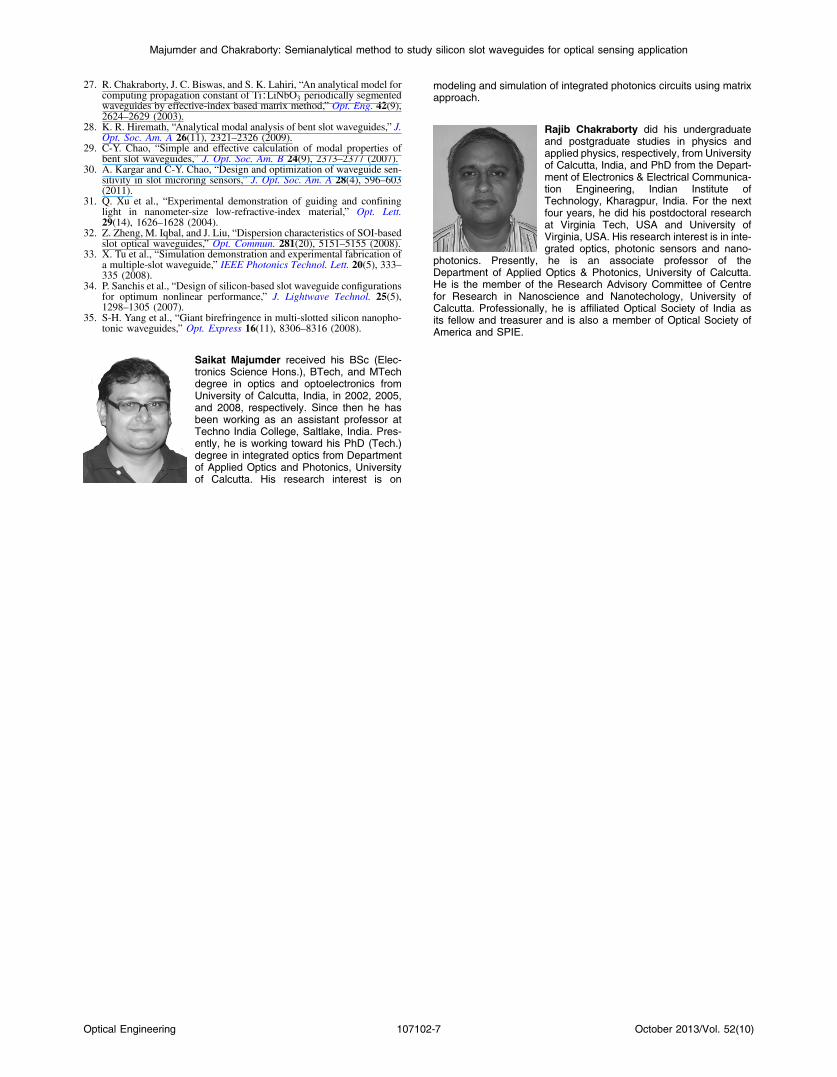
The responses of the slot waveguide for different refrac-tive indices of the slot region are also studied using EIMM.As in Fig. 6, two different cases have been studied here, too.It is seen that if the slot refractive index is varied, there ischange in peak electric field amplitude for all the cases.But while the change is more for variations of slab width
keeping slot width fixed (case 1), in comparison, the changein peak amplitude is not appreciable for case 2, i.e., for varia-tion of slot width keeping slab width fixed. The plots areshown in Fig. 7 and can be used to measure the contrastratio ½ðImax þ IminÞ∕ðImax − IminÞ� for use in high precisionsensing applications. Also, it is evident from Fig. 7, for afixed slot refractive index, the peak intensity increaseswith the slab width keeping the slot width fixed, and thepeak intensity decreases with an increase in slot width keep-ing the slab width fixed. In fact, this decay is exponential, asis shown in Fig. 8. Thus, from the last three figures, it is pos-sible to find the sensitivity and responsivity of slot wave-guide for different waveguide parameter variations. Thesestudies will be extremely important for sensing applicationof slot waveguide.
When slot waveguides are used for sensing application,the sensitivity will increase if more fraction of incidentlight power can interact with the sensing material, whichis kept in the slot region. Increasing slot width, however,decreases the peak intensity in the slot as can be seen inFig. 7. It has been reported in Ref. 35 that the power inthe slot region saturates if its width is increased, and to
Table 1 Effective index of different slot waveguides calculated using EIMM and its comparison with results obtained using numerical methods byother researchers.
Parameters Wavelength (λ, μm)
Effective index calculated using
Difference (in %) Ref. No.Our method Other method
wh ¼ 180 nm, ws ¼ 50 nm, h ¼ 300 nm,nh ¼ 3.48, ns ¼ nc ¼ 1.44
1.55 1.817 1.828 (FEM) 0.60 Ref. 32
1.59 1.797 1.796 (FEM) −0.0561.61 1.787 1.778 (FEM) −0.51
wh ¼ 180 nm, ws ¼ 100 nm, h ¼ 324 nm,nh ¼ 3.48, ns ¼ nc ¼ 1.33
1.55 1.582103 1.578638 (FEM) −0.22 Ref. 6
wh ¼ 220 nm, ws ¼ 100 nm, h ¼ 400 nm,nh ¼ 3.48, ns ¼ nc ¼ 1.46
1.55 1.9987687 2.028264 (BPM) 1.45 Ref. 34
Fig. 6 Effective index of slot waveguides with variation of slot refrac-tive index for different slot widths keeping slot width fixed (case 1) andfor different slab widths keeping slab width fixed (case 2).
Fig. 7 Normalized peak intensity of slot waveguides with variation ofslot refractive index. The parameters used are similar to that of Fig. 6.
Optical Engineering 107102-5 October 2013/Vol. 52(10)
Majumder and Chakraborty: Semianalytical method to study silicon slot waveguides for optical sensing application
increase the fraction of light in the low-index slot region,multiple slots will be required. So with multiple slots, sen-sitivity is supposed to increase. For its verification, the varia-tion of effective index with slot refractive index is plotted fora double slot waveguide and is shown in Fig. 9. As isexpected, the sensitivity has increased in a double slot wave-guide compared to a single slot waveguide (Fig. 6). Twocases, with parameters similar to that of Fig. 6, have beenstudied and their nature is similar to that of Fig. 6, butwith increased sensitivity. With a greater number of slots,even better sensitivity is expected.
4 ConclusionsThus, it can be concluded that EIMM, which has been suc-cessfully applied to low-index waveguide based devices, cannow be applied for high-index contrast waveguides. Highcontrast slab and slot waveguides were studied using EIMM,and the results match with the results obtained from other
numerical methods like FDTD, FEM, and BPM. EIMM,thus, provides a simple tool consisting of multiplication of2 × 2 matrices with minimum requirement of computermemory to analyze high-index contrast waveguide devices.Analysis of effective refractive index of slot waveguides fordifferent thicknesses and different refractive indices wasdone. Optimization of waveguide parameters for improvedsensitivity of the slot waveguide with sensing materialscan be performed for its use as sensor. It is expected thatthis method can be applied to more complex waveguidecross-sections as well as bend waveguides.
References
1. V. R. Almeida et al., “Guiding and confining light in void nanostruc-ture,” Opt. Lett. 29(11), 1209–1211 (2004).
2. H. Rong et al., “An all-silicon Raman laser,” Nature 433(7023), 292–294 (2005).
3. Y.-H. Kuo et al., “Demonstration of wavelength conversion at 40 Gb∕sdata rate in silicon waveguides,” Opt. Express 14(24), 11721–11726(2006).
4. R. Salem et al., “All-optical regeneration on a silicon chip,” Opt.Express 15(12), 7802–7809 (2007).
5. Q. Xu and M. Lipson, “All-optical logic based on silicon micro-ringresonators,” Opt. Express 15(3), 924–929 (2007).
6. F. Dell’Olio and V. M. Passaro, “Optical sensing by optimized siliconslot waveguides,” Opt. Express 15(8), 4977–4993 (2007).
7. A. Di Falco, L. O’Faolain, and T. F. Krauss, “Chemical sensing in slot-ted photonic crystal heterostructure cavities,” Appl. Phys. Lett. 94(6),063503 (2009).
8. J. T. Robinson, L. Chen, and M. Lipson, “On-chip gas detection in sil-icon optical microcavities,” Opt. Express 16(6), 4296–4301 (2008).
9. C. A. Barrios et al., “Slot-waveguide biochemical sensor,” Opt. Lett.32(21), 3080–3082 (2007).
10. M. Li, W. H. P. Pernice, and H. X. Tang, “Ultrahigh-frequency nano-optomechanical resonators in slot waveguide ring cavities,” Appl. Phys.Lett. 97(18), 183110 (2010).
11. Y. Li et al., “Design of dispersive optomechanical coupling and coolingin ultrahigh-Q/V slot-type photonic crystal cavities,” Opt. Express18(23), 23844–23856 (2010).
12. J.-M. Brosi et al., “High-speed low-voltage electro-optic modulator witha polymer-infiltrated silicon photonic crystal waveguide,” Opt. Express16(6), 4177–4191 (2008).
13. C. Koos et al., “Nonlinear silicon-on-insulator waveguides for all-opti-cal signal processing,” Opt. Express 15(10), 5976–5990 (2007).
14. T. Vallaitis et al., “Optical properties of highly nonlinear silicon-organichybrid (SOH) waveguide geometries,” Opt. Express 17(20), 17357–17368 (2009).
15. J. Wulbern et al., “Electro-optic modulation in slotted resonant photoniccrystal heterostructures,” Appl. Phys. Lett. 94(24), 241107 (2009).
16. C. Koos et al., “All-optical high-speed signal processing with silicon-organic hybrid slot waveguides,” Nat. Photon. 3(4), 216–219 (2009).
17. T. Baehr-Jones et al., “Optical modulation and detection in slotted sil-icon waveguides,” Opt. Express 13(14), 5216–5226 (2005).
18. Z. Gaburro, “A design for a photonic syringe with multimode coupledslot waveguides,” Opt. Express 18(4), 288–300 (2010).
19. A. H. J. Yang et al., “Optical manipulation of nanoparticles and biomo-lecules in sub-wavelength slot waveguides,” Nature 457(7225), 71–75(2009).
20. A. H. J. Yang, T. Lerdsuchatawanich, and D. Erickson, “Forces andtransport velocities for a particle in a slot waveguide,” Nano Lett.9(3), 1182–1188 (2009).
21. A. K. Ghatak, K. Thyagarajan, and M.R. Shenoy, “Numerical analysisof planar optical waveguides using matrix approach,” J. LightwaveTechnol. 5(5), 660–667 (1987).
22. A. K. Ghatak, K. Thyagarajan, and M. R. Shenoy, “A novel numericaltechnique for solving the one-dimensional schrödinger equation usingmatrix approach-application to quantum well structures,” IEEE J.Quantum Electron. 24(8), 1524–1530 (1988).
23. K. Thyagarajan, M. R. Shenoy, and A. K. Ghatak, “Accurate numericalmethod for the calculation of bending loss in optical waveguides using amatrix approach,” Opt. Lett. 12(4), 296–298 (1987); Erratum: OpticsLetters (March 1989).
24. M. R. Shenoy, K. Thyagarajan, and A. K. Ghatak, “Numerical analysisof optical fibers using matrix approach,” J. Lightwave Technol. 6(8),1285–1291 (1988).
25. R. Chakraborty et al., “Integrated optical waveguides in LiNbO3:modelling and experimental analysis,” Proc. SPIE 4417, 278–285(2001).
26. R. Chakraborty, J. C. Biswas, and S. K. Lahiri, “Analysis of directionalcoupler electro-optic switches using effective–index-based matrixmethod,” Opt. Commun. 219(1–6), 157–163 (2003).
Fig. 8 Normalized peak intensity of slot waveguides with variation ofslot width for a fixed slot refractive index and its exponential fittingcurve.
Fig. 9 Effective index of a double slot waveguides with variation ofslot refractive index. Parameters are same as in Fig. 6.
Optical Engineering 107102-6 October 2013/Vol. 52(10)
Majumder and Chakraborty: Semianalytical method to study silicon slot waveguides for optical sensing application
27. R. Chakraborty, J. C. Biswas, and S. K. Lahiri, “An analytical model forcomputing propagation constant of Ti∶LiNbO3 periodically segmentedwaveguides by effective-index based matrix method,” Opt. Eng. 42(9),2624–2629 (2003).
28. K. R. Hiremath, “Analytical modal analysis of bent slot waveguides,” J.Opt. Soc. Am. A 26(11), 2321–2326 (2009).
29. C-Y. Chao, “Simple and effective calculation of modal properties ofbent slot waveguides,” J. Opt. Soc. Am. B 24(9), 2373–2377 (2007).
30. A. Kargar and C-Y. Chao, “Design and optimization of waveguide sen-sitivity in slot microring sensors,” J. Opt. Soc. Am. A 28(4), 596–603(2011).
31. Q. Xu et al., “Experimental demonstration of guiding and confininglight in nanometer-size low-refractive-index material,” Opt. Lett.29(14), 1626–1628 (2004).
32. Z. Zheng, M. Iqbal, and J. Liu, “Dispersion characteristics of SOI-basedslot optical waveguides,” Opt. Commun. 281(20), 5151–5155 (2008).
33. X. Tu et al., “Simulation demonstration and experimental fabrication ofa multiple-slot waveguide,” IEEE Photonics Technol. Lett. 20(5), 333–335 (2008).
34. P. Sanchis et al., “Design of silicon-based slot waveguide configurationsfor optimum nonlinear performance,” J. Lightwave Technol. 25(5),1298–1305 (2007).
35. S-H. Yang et al., “Giant birefringence in multi-slotted silicon nanopho-tonic waveguides,” Opt. Express 16(11), 8306–8316 (2008).
Saikat Majumder received his BSc (Elec-tronics Science Hons.), BTech, and MTechdegree in optics and optoelectronics fromUniversity of Calcutta, India, in 2002, 2005,and 2008, respectively. Since then he hasbeen working as an assistant professor atTechno India College, Saltlake, India. Pres-ently, he is working toward his PhD (Tech.)degree in integrated optics from Departmentof Applied Optics and Photonics, Universityof Calcutta. His research interest is on
modeling and simulation of integrated photonics circuits using matrixapproach.
Rajib Chakraborty did his undergraduateand postgraduate studies in physics andapplied physics, respectively, from Universityof Calcutta, India, and PhD from the Depart-ment of Electronics & Electrical Communica-tion Engineering, Indian Institute ofTechnology, Kharagpur, India. For the nextfour years, he did his postdoctoral researchat Virginia Tech, USA and University ofVirginia, USA. His research interest is in inte-grated optics, photonic sensors and nano-
photonics. Presently, he is an associate professor of theDepartment of Applied Optics & Photonics, University of Calcutta.He is the member of the Research Advisory Committee of Centrefor Research in Nanoscience and Nanotechology, University ofCalcutta. Professionally, he is affiliated Optical Society of India asits fellow and treasurer and is also a member of Optical Society ofAmerica and SPIE.
Optical Engineering 107102-7 October 2013/Vol. 52(10)
Majumder and Chakraborty: Semianalytical method to study silicon slot waveguides for optical sensing application