Bulk heterojunction solar cells with internal quantum efficiency approaching 100
Upload
independentCategory
view
0download
0
JOURNAL OF APPLIED PHYSICS VOLUME 86, NUMBER 11 1 DECEMBER 1999
Light emitting porous silicon diode based on a silicon/poroussilicon heterojunction
L. Pavesia) and R. ChierchiaIstituto Nazionale di Fisica della Materia and Dipartimento di Fisica, Universita` di Trento, Via Sommarive14, I-38050 Povo (TN), Italy
P. Bellutti and A. LuiDivisione Microsistemi, ITC-IRST, via Sommarive, I-38050 Povo (TN), Italy
F. Fuso, M. Labardi, L. Pardi, F. Sbrana, and M. Allegrinib)
Istituto Nazionale di Fisica della Materia and Dipartimento di Fisica, Universita` di Pisa,Via F. Buonarroti 2, I-56127 Pisa, Italy
S. Trusso and C. VasiIstituto di Tecniche Spettroscopiche del CNR, Via La Farina 237, 98123 Messina, Italy
P. J.Ventura, L. C. Costa, and M. C. CarmoDepartamenta de Fisica, Universidade de Aveiro, 3800 Aveiro, Portugal
O. BisiIstituto Nazionale di Fisica della Materia and Dipartimento di Scienze e Metodi dell’Ingegneria, Facolta` diIngegneria, Sede di Reggio Emilia, Universita` di Modena e Reggio Emilia, 42100 Reggio Emilia, Italy
~Received 22 February 1999; accepted for publication 30 August 1999!
A new structure is proposed to improve the external quantum efficiency of porous silicon~PS! lightemitting diodes~LED!. It is based on a heterojunction betweenn-type doped silicon and PS. Theheterojunction is formed due to the doping selectivity of the etching process used to form PS. Theimprovement of the proposed LED structure with respect to usual metal/PS LED is demonstrated.This is thought to be due to a different injection mechanism for which carriers are injected directlyinto conduction band states. Anodic oxidation experiments show further improvements in the LEDefficiency. © 1999 American Institute of Physics.@S0021-8979~99!07123-6#
t
n
oteluisfo
nes
c-
r
,
e
hethe
n atkyto
ace
dlethe
essthese
on
oles
nare
olo6
I. INTRODUCTION
Light emitting diodes~LED! share a worldwide markewhich is much larger than that of lasers. This is due to:~i!the lower stringent requirements for their production,~ii ! thelarger reliability caused by a lower power consumption aby the independence on the working temperature, and~iii !the reachable high brilliance. On the other hand, the demstration of an efficient laser action in a silicon based syswill have a great impact on optoelectronics, and will revotionize the emerging field of photonics. A first step to thgoal is the demonstration of an efficient Si based LEDwhich porous silicon~PS! is a good candidate.1 State of theart PS based LED devices have external quantum efficieof more than 1% even if the power efficiency is still in thorder of 0.1%, due to the very high turn-on voltage of thediodes,2 while integration of PS based LED with microeletronic circuit has also been demonstrated.3
Let us concentrate on some basic aspects. The extequantum efficiency,hext, of a LED is hext}h int3h inj
3hextract,4 where: h int is the internal quantum efficiency
which for PS is relatively high (.10%); h inj is the carrierinjection efficiency, which depends on both the junction us
a!Electronic mail: [email protected]!On sabbatical leave from Dipartimento di Fisica della Materia e Tecn
gie Fisiche Avanzate, Universita` di Messina, Salita Sperone 31, I-9816Sant’Agata~ME!, Italy.
6470021-8979/99/86(11)/6474/9/$15.00
d
n-m-
r
cy
e
nal
d
and the transport properties of the active material;hextract isthe extraction efficiency, which rules the extraction of tphotons generated into the device and depends on bothgeometry and refractive index of the system.
The first generation of PS based LED was based ometal deposition on top of the PS layer to obtain a Schotbarrier.5,6 However, the metal/PS junction was observedact as an ohmic contact due to a large density of interfstates which pins the Fermi level at the midgap.7 Electronsare injected from the metal into the defect band in the midof the PS bandgap. No rectification was measured whenPS layer thickness was large. On the contrary, rectifyingI–Vcharacteristics were observed when the PS layer thicknwas small due to the presence of a heterojunction atPS/silicon wafer interface. Typical efficiencies of theLEDs were in the order of 1024%. More efficient injectionwas obtained by using LED exploiting PS homojuncti~second generation of devices!.8–10 These were formedthrough the anodic etch ofp/n silicon junctions. Externalefficiencies up to 0.8% were measured in such devices.10 Aremark is here necessary: bothp/n andn/p porous homojunc-tions show highhext values.3,10 No difference in injectionefficiency was measured when the top contact injects hor electrons.
Very recently, another increase ofh inj has been obtainedby using anodic oxidization.2 This improvement is based othe electrical isolation of those conducting paths which
-
4 © 1999 American Institute of Physics

laino
ugha
wffithopis
thheilt
nn
iee
rtsthce.urnithncr-Sereoni
e
nginn
LE.
the
om-b
et athe
bles-
le-
-nalro-d in
4
o-
l-
5
.8e
by
-
c-
at-orrger
6475J. Appl. Phys., Vol. 86, No. 11, 1 December 1999 Pavesi et al.
not luminescent, such as those formed by sequences ofnanocrystals. Indeed anodic oxidation is obtained by usan electrochemical process: the oxidation develops firstlythose PS regions where the current flows easily, i.e., throlarge nanocrystals. External quantum efficiencies larger t1% are found, even though the LEDs used are basedPS/metal contact.
Based on these observations it is deduced that oneto improve PS based LED is to maximize the injection eciency into the luminescent nanocrystals. We think thatmajor bottleneck is the injection into PS through the tsurface. We conceived that a natural clean interface exbetween PS and the silicon wafer at the interior ofsample. If one is able to mimic this interface as well for ttop electrode, the injection efficiency of PS based LED wbe improved. In this article, we present a tentative wayimprovehext of PS based LED, by trying to increaseh inj . Toobtain this we exploit the doping selectivity of the silicoanodization. When the etch is performed in the dark owafer wherep-type regions facen-type regions, only thep-type regions are etched. Thus crystallinen-type regions areinterfaced with porous regions. In addition, oxidation studare also performed to electrically isolate the non-luminescbut highly conductive paths.
This article is organized as follows: Section II repothe rational of our proposed structure which is based onformation of ann1-type doped Si/PS heterointerface; SeIII refers to the issue of formation of PS; Sec. IV discussthe problem of underetching then1-type doped regions; SecV reports on both an investigation of the sample structthrough micro-Raman spectroscopy and near-field scanmicroscopy; Sec. VI refers to the discussion of the role ofn1-type doped regions in improving the electroluminesceof the LED; Sec. VII presents a simple model of the diffeences between our device and metal/PS based LED;VIII reports on alternate current~ac! measurements of thLED conductivity. Pulsed excitation experiments are psented in Section IX, while stability tests in Sec. X. SectiXI reports on anodic oxidation experiments. The articleconcluded in Sec. XII by a summary of the results andcritical review. Preliminary characterizations of these dvices have been published in Refs. 11 and 12.
II. DEVICE LAYOUT AND RATIONAL
The silicon/PS heterointerface is realized by exploitithe doping selectivity of the PS formation. Once the etchis performed in the dark and with relatively low current desities,n-type doped layers are not etched whilep-type dopedones are homogeneously etched. Thus, we designed abased on an heterojunction betweenn-type doped Si and PSThe various requirements to fulfil were:
~1! the n-type doped regions are used to inject carriers:interface between these regions and PS should blarge as possible to maximize the injection;
~2! the light generated in the PS layer should come out frthe LED: the crystallinen-type doped regions which absorb the light, should be thin enough to minimize asorption;
rgegnhn
on
ay-e
tse
lo
a
snt
e.s
engee
ec.
-
sa-
g-
D
eas
-
~3! the junction depth between then-type regions and thep-type doped substrate should be shallow enough to lcomplete underetching of the substrate even undern-type doped regions;
~4! the processing should be compatible with the availatechnology at our disposition within ITC-IRST for a posible CMOS integration;
~5! the layout should be simple to focus mainly on the roof the n-type doped regions, thus leaving further improvements for the future.
Unfortunately we were not able to fulfill all these requests. A compromise solution was needed. The fischeme we used is shown in Fig. 1. A summary of the pcessing sequence as well as of the device layout is listethe following:
~1! the test structure is an array of 250n1-type doped stripes~6 mm wide, 8 mm long, 0.5mm deep, and spaced 3mm apart! in a p-type doped region;
~2! the n1 finger structure diodes are defined by a lithgraphic step on~100! oriented Czochralski grown 20V cm p-type Si wafers. As ion implantation and the folowing annealing at 975 °C producen1/p diodes with ajunction depth of 0.5mm and a sheet resistance of 3V/h;
~3! every 4 in. wafer has four implanted regions (030.8 cm2) which are evidenced by slightly etching thp-type doped regions;
~4! an ohmic contact is formed on the back of the waferB implantation, Al deposition and sintering at 400 °C;
~5! the wafers are cut into 232 cm2 samples, each containing a test structure;
~6! PS silicon is formed as discussed in the following setion;
~7! Al top contacts are formed by Al evaporation and pterned through a metal mask into circular, fingered,square pads of various thicknesses. Al thicknesses la
FIG. 1. Top view and cross section of the device.

oant t
bP
aheths
elTnale
e-ts
is.5
eo
.int oodghitPad-a
or
lin
thbo
hee-
t i
cetant
Si
lnd,
allyes
se-up
t ofe isby
Dea-era-
--
eakob-
-
6476 J. Appl. Phys., Vol. 86, No. 11, 1 December 1999 Pavesi et al.
than 300 nm are routinely used. These values turnedto be the minimum necessary to have reproduciblestable I–V characteristics. These are not transparenvisible light.
III. PS PRODUCTION
A 1.8 cm2 circular area of the 232 cm2 sample wasrendered porous through a standard electrochemical etch~seeRef. 6!. Various HF concentrations have been used~15%,20%, and 30% HF concentration in volume! within an etha-nol solution. The drying of the samples was performedusing methanol and pentane to minimize cracking of thelayer.
The high resistivity of the available wafers requiredparticular care to assure repeatibility and uniformity of tetched layers. The critical issue is the homogeneity ofcurrent through the sample during the etch. To this purpoa mild HF cleaning of the back of the sample was routinused in order to remove the aluminum oxide formed.increase the homogeneity of the PS layer, a weak illumition ~halogen lamp 500 W, 25 cm apart from the samp!was also used.
It is known that the PS of high porosity realized on rsistive substrates is very fragile and easily detaches fromsubstrate during the drying and the subsequent processteps~Al evaporation and electrical bonding!. The choice ofthe HF concentration in the solution was critical with threspect. With a 15% HF solution uniform PS films up to 2mm thick for high porosities~70%! and 30mm thick for lowporosities~40%! were obtained. With a 30% HF solution throbustness of the PS layer and their homogeneity were measily obtained and thicknesses up to 45mm can be obtainedOn the other hand, the luminescence intensity of PS obtawith a 30% HF solution was much less intense than thaPS obtained with a 15% HF solution. Therefore a tradewas needed. We decided to use a 15% HF solution anform multilayer structures where alternatively low and hiporosity layers are obtained by varying the current densIn this way, one can obtain robust and high luminescentfilms. Unless otherwise stated, the LED presented here hPS thickness of 2.5mm and are formed by a multilayer structure of 16 periods where the current during the etch wmodulated between 5 and 27.78 mA cm22 for 13 and 5.41 s,respectively.
IV. CRYSTALLINE STEM
Then1-type doped stripes are not etched during the fmation of PS in thep-type doped region.11,12 However thestripes are not floating over the PS layer, but a crystalstem is visible under the stripes~see the inset in Fig. 2!. Thisstem is the result of an incomplete underetching due toanisotropy of the etching process. The dependence ofthe PS layer thickness~d! and the stem width~p! on theetching time for two HF concentrations is reported in tinset of Fig. 2.d is linearly dependent on the etching timwhile p is not. Forp<0.5 mm the lateral etching rate decreases dramatically. Figure 2 shows the dependence ofp ond for various HF concentrations and current densities. I
utdo
yS
ee,yo-
heing
re
edf
ffto
y.Sa
s
-
e
eth
s
observed thatp mainly depends ond up tod.5 mm as it isexpected for an isotropic etch. For largerd, p is slowly re-duced and one needs ad.20 mm in order to completelyremove the stem, i.e., to realize floatingn1 stripes on PS.Among the various facts which contribute to the occurrenof the etch anisotropy we speculate that the most imporare:
~i! H2 bubbles sticking under then1-stripes, which forma region oversaturated with H slowing down thedissolution reactions;
~ii ! the reduction of the stem width,p, increases the locaresistance reducing the current through the stems ahence, reducing the etching rate.
A confirmation of the role of H2 sticking, has been foundin a dedicated experiment where the sample was verticplaced in the electrochemical cell, thus having the striphorizontally aligned. An asymmetry in the stems was subquently measured: the etch was faster on the side facingwhile it was slower on the side facing down. Indeed, H2
bubbles could more easily escape from the side-up parthe stem than from the side down. However, the resistancalso playing an important role. It has been reported thatusing a largerp-type doping under then1 region the un-deretching is more effective.13
V. OPTICAL TOPOLOGY OF THE SAMPLES
A. Raman measurements
Through a double monochromator coupled to a CCcamera and to an optical microscope it was possible to msure the spatially resolved Raman spectra at room tempture of our devices. The exciting laser light~wavelength of488 nm! was focused to a diameter of 1.5mm. The energyresolution of the spectra was 0.4 cm21. A series of measurements along a line between twon1 stripes have been performed. Each measurement point was 3.8mm apart. Figure 3reports some of the results. A clear dependence of the ppositions and linewidths on the measurement point is
FIG. 2. Dependence of of the stem width~p! on the PS layer thickness~d!.The various symbols refer to different HF concentrations~squares 15%,triangles 30%). The dependence of the PS layer thickness~top panels! andof the stem width~bottom panels! on the etching time for two HF concentrations @~a! 30% HF and current density 150 mA/cm2, ~b! 15% HF andcurrent density 27.78 mA/cm2] is shown in the insets.

ryth
ontae
totowim
w-aht 2
ligS
ro-ace-nm
axi-
ap-llyen
ncer.ex-lu-
gths
of
ite
hrge
e
l-s.
6477J. Appl. Phys., Vol. 86, No. 11, 1 December 1999 Pavesi et al.
served. When the laser is focused onto then1 stripes nodifference between the measured Raman spectra andspectra of crystalline silicon is observed. The.520 cm21
peak is due to optical phonons in silicon. On the contrawhen the laser light is focused onto the PS formed amongvariousn1 stripes, a softening and widening of the phonpeak are both observed. The line shape is almost consover the PS surface suggesting a good degree of homogity of the PS.
It is well known that the phonons in PS are confined inSi nanocrystals.14–16 Various models have been reportedrelate the experimentally measured phonon lineshapethe critical dimensions of the nanocrystals. Here we assuthe validity of the strong phonon confinement model andconsider spherical nanocrystals.15 The results of this theoretical analysis are reported in Fig. 4: the peak positionsrelated to the nanocrystal sizes. In the center of the etcregion the sizes are almost constant and equal to abounm. The apparent increase of the sizes as then1 stripes areapproached is due an experimental artifact, i.e., to somewhich is diffused by the crystalline regions. Being theRaman cross section much larger than that of PS, thecontribution overcomes and hinders the PS contribution.
FIG. 3. Raman spectra of a LED before the Al deposition measured on tdifferent points A, B, and C.vo is peak position. The inset shows an imaof the sample surface with indicated A, B, and C points. The samples wformed by an etch in 30% HF at a current density of 150 mA/cm2 for 61.17s.
FIG. 4. Peak positions~left-hand side axis! and corresponding nanocrystaline sizes~right-hand side axis! as a function of the position on the deviceIn the back ground an image of the sample surface is reported.
the
,e
ntne-
the
e
reed.6
htiSiB. Scanning near-field optical microscopy „SNOM…
measurements
Scanning near-field optical microscopy~SNOM!17 andspectroscopy18 have been used for spatially resolved spectscopic analysis of the luminescence from a LED with a spresolution below the diffraction limit for visible light. Photoluminescence maps with a resolution up to 50–100have been previously achieved on PS19,20 while Raman andother nonlinear spectroscopies are usually limited to a mmum resolution of 150–200 nm.21 In this article, we operateSNOM spectroscopy in the emission mode, i.e., a smallerture is used as a quasi-point-like light emitter to locaexcite the sample. The light emitted from the sample is thcoupled to a multimode optical fiber and sent to the entraslit of a monochromator equipped with a photomultiplieWhen the selected wavelength corresponds to that of thecitation, a scattering image is recorded; otherwise, photominescence maps are obtained by selecting wavelen
FIG. 5. SNOM images of a sample produced with a HF concentration15%, an etching time of 600 s with a current density of 27.78 mA/cm2;topographical image~a!, scattered light image atlcoll5lexc5690 nm ~b!,photoluminescence image atlcoll5640 nm,lexc5458 nm~c!. Inset~d! re-ports the results of the line profile analysis for the row highlighted in whin insets ~a! ~topography — solid line! and ~c! ~emission at 640 nm —dotted line!.
ee
re
rta
ctenigcei
hurran
–2alitto
tord
g
o
fn
necifita
anige
thti
ndc-ic
St
idth
stly
est, thefer-cha-e-
-aths
ncesin-
that
sthe
heeas-
ys-ith
ar-ob-tely
oute
hetheethean-
6478 J. Appl. Phys., Vol. 86, No. 11, 1 December 1999 Pavesi et al.
within the emission spectrum. In our instrument backwacollection is accomplished at 45° by means of a long frondistance microscope objective.
Our homemade SNOM,22 working in the emission modeand reflection configuration, has been used for the charaization of a sample which, on purpose, was not dried in ptane, and thus cracks were present on the PS surface. F5~a! shows the topographical image of a portion of surfataken at the smallest possible magnification of our SNOMorder to visualize the full width of ann1 stripe, visible as athick white line. The side regions correspond to PS. Ttypical fracture of PS due to capillary forces developed ding the drying process are observed as dark regions. Ftures are some microns deep. The surface of PS is showgreyish; its average roughness is measured about 100nm. Figure 5~b! is a simultaneously acquired SNOM opticimage obtained by setting the monochromator on the exction wavelength (lcoll5lexc5690 nm!. In this measuremenscattered light intensity is related to the optical propertiesthe sample; here then1 stripe appears as a white line duea higher scattering than PS. Dark line sides are due to boeffects and do not represent a different material. Figure 5~c!is the PL map of the device at the emission peak wavelen(;640 nm! when excited with Ar1 laser at 458 nm. In thePS region, a quite homogeneous emission is observed. Sweak evidence of bright spots is present. Then1 stripe re-gion shows some residual emission, probably due to thefield background of SNOM. More detailed information othe local distribution of the emission are provided by liprofile analysis of the luminescence map, where a sperow of the map is analyzed as a function of the horizonposition. An example is shown in Fig. 5~d!, where a com-parison between line profile analysis of the topographyof the emission map at 640 nm is presented. The row hlighted in white in panels~a! and ~c! has been used for thanalysis. A step due to the presence of then1 stripe region isevident in the topography; corresponding to the step,emission intensity exhibits a sharp decrease, demonstrathat the emission occurs essentially in the PS region.
VI. ROLE OF n 1 STRIPES
A. Electrical injection
The first aim of our investigation was to understawhether then1-stripes played any role in the carrier injetion process or not. For this reason we compared two devrealized on 45mm thick samples: one wheren1 stripes werepresent~test device! and the other with the usual metal/Pjunctions ~control device!. For the latter device, an almossymmetricI–V characteristic is measured~see Fig. 3 in Ref.11!. This behavior is well known in the literature7 and it isthe consequence of the ohmic behavior of the metal/PSterface where carrier injection into surface states pinnethe Fermi level of the PS silicon occurs. On the contrary,test device shows a rectifyingI–V characteristic~rectificationof 250 at 5 V! typical of a diode behavior where then1
stripes/PS interface behaves as a junction: forward bianeeded to overcome the built-in barrier and to efficieninject electrons into PS. We mention that ford545 mm the
dl
er--
ure,
n
e-c-as00
a-
f
er
th
me
ar
cl
dh-
eng
es
n-ate
is
n1 stripes are completely floating over PS~see Fig. 2!. Forforward bias, a much larger current is injected into the tdevice than for the reference diode. When reverse biasedtest device shows a larger saturation current than the reence device. These data indicate that the transport menisms are completely different in the test and control dvices.
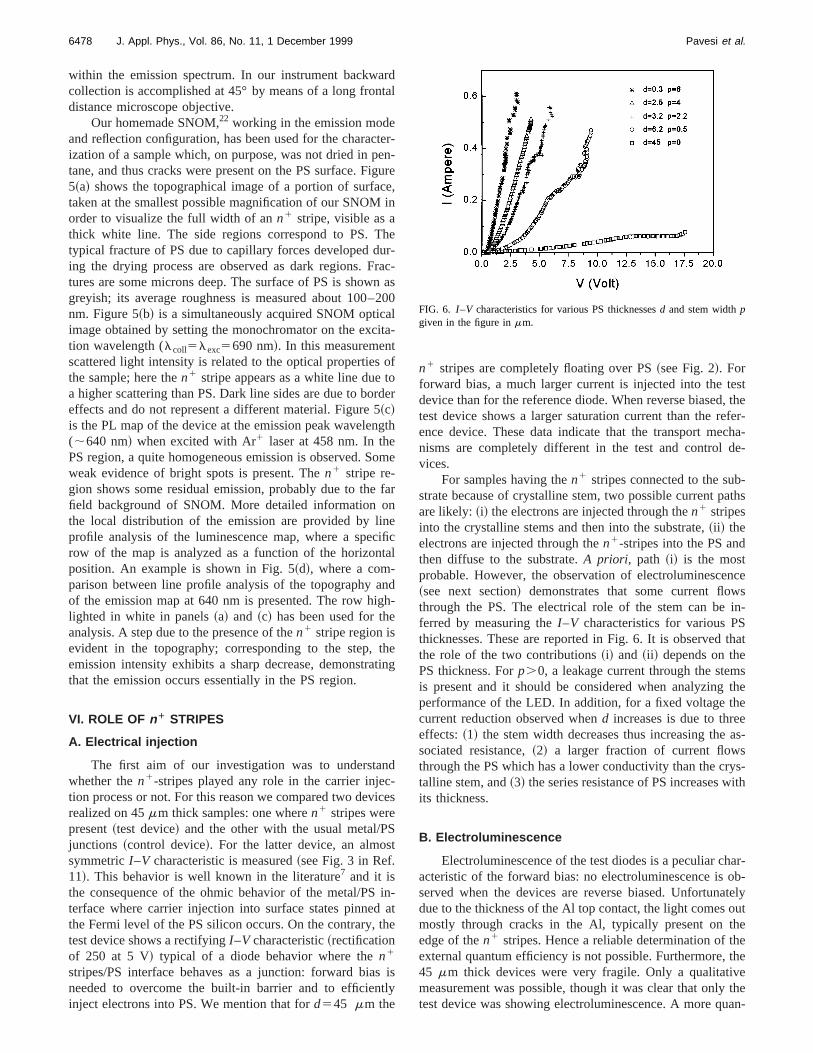
For samples having then1 stripes connected to the substrate because of crystalline stem, two possible current pare likely:~i! the electrons are injected through then1 stripesinto the crystalline stems and then into the substrate,~ii ! theelectrons are injected through then1-stripes into the PS andthen diffuse to the substrate.A priori, path ~i! is the mostprobable. However, the observation of electroluminesce~see next section! demonstrates that some current flowthrough the PS. The electrical role of the stem can beferred by measuring theI–V characteristics for various PSthicknesses. These are reported in Fig. 6. It is observedthe role of the two contributions~i! and ~ii ! depends on thePS thickness. Forp.0, a leakage current through the stemis present and it should be considered when analyzingperformance of the LED. In addition, for a fixed voltage tcurrent reduction observed whend increases is due to threeffects:~1! the stem width decreases thus increasing thesociated resistance,~2! a larger fraction of current flowsthrough the PS which has a lower conductivity than the crtalline stem, and~3! the series resistance of PS increases wits thickness.
B. Electroluminescence
Electroluminescence of the test diodes is a peculiar chacteristic of the forward bias: no electroluminescence isserved when the devices are reverse biased. Unfortunadue to the thickness of the Al top contact, the light comesmostly through cracks in the Al, typically present on thedge of then1 stripes. Hence a reliable determination of texternal quantum efficiency is not possible. Furthermore,45 mm thick devices were very fragile. Only a qualitativmeasurement was possible, though it was clear that onlytest device was showing electroluminescence. A more qu
FIG. 6. I–V characteristics for various PS thicknessesd and stem widthpgiven in the figure inmm.

tllira
hehe
tnanELic
he.assthth
avitsate
itythv
n
eif
te
ntes.
-in
tionthe
n-the
cen-ingonns-
hed by
di-ia-
on aen-75
thea
is
e-
ofativeare
pd
he
6479J. Appl. Phys., Vol. 86, No. 11, 1 December 1999 Pavesi et al.
titative analysis is possible when using thinner devices buthis case the leakage current passing through the crystastems complicates the interpretation of the efficiency calibtion. An indication of efficiency is possible by measuring ttypical current density to obtain light visible to eyes in tdark: for the test LED it is in the interval 50–150 mA/cm2.
In Ref. 11 we reported the EL-I characteristics of the tesLED and of a reference LED: an improvement of about oorder of magnitude was observed comparing the testreference LED. A further clear difference between thecharacteristics of these devices is that the reference devshow light emission only around the Al contact while for ttest devices the emission is also spread along the stripesrecognize the origin of the EL a comparison with PL wperformed~see Fig. 5 in Ref. 11!. Since the emission peakwere almost the same in both case, the origin of the EL isrecombination of excitons in the nanocrystals present inPS layer. No hot electron emission was observed.
Moreover, by comparing the EL spectra of samples hing different stem widths, no dependence of the EL intenson the PS layer thickness has been measured. Since thesamples have shown a clear difference in terms of injeccarriers~see Fig. 6! and since the electroluminesce intensis connected to the current flowing through the PS layers,above reported independence suggests the existence of athin layer near then1-stripe/PS heterointerface whose quatum efficiency is very high.
VII. TRANSPORT MODEL
In order to explain the observed differences betwemetal/PS andn1-stripes/PS devices we suggest that they dfer for the energy states into which the electrons are injecThe control device is described by the model proposed
FIG. 7. Schematic band structure diagram of a metal/PS device~top panel!and of the test device~bottom panel!. CB and VB refer to the conductionand valence effective bands which roughly approximate the lowest emand the highest filled quantum confined states of the various quantumwhich form porous silicon.
inne-
ed
es
To
ee
-ymed
eery-
n-d.in
Ref. 7 ~Fig. 7, top panel!: the interface metal/PS acts as aohmic contact and electrons are injected into midgap staThis explains two main facts:~1! the I–V characteristic issymmetric, and~2! the EL intensity is low. In fact, to recombine by emission of visible light, the electrons have to gaenergy to move from the midgap states to the conducband states. We propose that, in the test device,n1-stripes/PS junction acts as a standardn/p heterojunction~Fig. 7 bottom panel!: the electrons are injected into the coduction band. This could be due to a better interface thanmetal/PS interface which reduces the midgap defect contration. This explanation accounts for the observed rectifybehavior of the test device. In addition, the larger injectiefficiency could also be explained by considering the traport properties of conduction band states~even if formed inquantum dots! as compared to those of trap states. Thigher quantum efficiency of the devices is also addressethis model whenever one considers that the electrons arerectly injected into those states from which they can radtively recombine.
VIII. ac CONDUCTIVITY
ac conductivity measurements have been performedfew devices. Through a Solartron 126 model for the frequcies range 1 Hz–100 KHz and an HP 4285A model forKHz–5 MHz, the impedance and the phase angle~Z andf)with respect to a known reference was measured. ThenresistivityR and the capacityC are calculated by assumingparallel impedance: Z5R/A11(vRC)2 and tan(f)5vRC. From these measurements, the ac conductivityderived through:
sac~v!5L
AR~v!, ~1!
whereL and A are the thickness and the surface of the dvice, through which the current flows. For our devices,A isthe whole PS surface. In Fig. 8 we show a typical resultsuch a measurement for a test LED. These are representof various measurements on different LED. Two regimesfound: a low frequency regime (v<13105 Hz! wheresac is
tyots
FIG. 8. ac conductivity as a function of the frequency for a test LED. Tfitting of the data points with the theory@Eq. ~2!# is given by a line. Theparameters extracted from the fit are reported in the figure.

isere
hby
ePSncrchhaeis
su
llihouPa
f
in
ifthti
set
ri-ED
d9
oureen
Llledve
rteda.set.anditytillpar-n-s.
henr in
by
/en
du
ous
rented
6480 J. Appl. Phys., Vol. 86, No. 11, 1 December 1999 Pavesi et al.
almost independent onv and a high frequency regime (v>13105 Hz! wheresac shows a quadratic dependence. This in contrast to the behavior of crystalline Si diodes whsac is independent onv. To compare our data with thosreported in the literature,23,24 we have fitted our data with
sac5G01Avu1v2Css
2 Rss
11~vCssRss!2
, ~2!
where the fitting parameters are reported in Fig. 8. Tmodel assumes that the measured conductivity is givenbulk PS conductivity@first two terms of Eq.~2!# and by acontribution due to the contact resistance23 or to surfacestates24 @last term of Eq.~2!#. It is interesting to discuss thlow frequency regime which is that dominated by thebulk conductivity and which shows a power-law dependeof sac. The exponentu.0.2 that we have found is lowethan the.0.5 value reported in both Refs. 23 and 24 whiwas obtained by using metal/PS devices. In particular, itbeen shown in Ref. 23 that theu parameter is related to thrandom walk dimension of walkers on a fractal lattice. Thshould indicate that the conducting network we are meaing is different from that measured in the other works.23,24
Though the presence of leakage path through the crystastem could complicate this simple analysis, we believe tthis finding is supporting the model presented in the previsection: the injection of carriers when metal/PS or Si/junctions are considered is into different states: midgstates and conduction band states. Finally, from theu.0.2value we have found and following the definitions of Re23, it is possible to deduce the fractald̄.1.9 and the fractond̃.1.5 dimensions. These correlate well withd̄52 found inx-ray scattering experiments for 68% porosity layers25 andwith d̃51.2– 1.5 for diffusive electron transport foundother fractal materials.26
IX. PULSED EXCITATION
The external quantum efficiency of this device was dficult to determine because of the thick Al contact andleakage current through the crystalline stems. Conservaestimation gives an inferior limit of 231024. Despite this
FIG. 9. Normalized electroluminescence intensity as a function of theration of the current pulse (ton) and for two different periods (T51 msdiscs,T510 ms squares!.
e
ea
e
s
r-
neats
Sp
.
-eve
low value, the current and voltage corresponding to the onof visible electroluminescence~40 mA/cm2 and 10 V, re-spectively! are very encouraging. Pulsed injection expements have shown that the efficiency of the PS based Lcan be increased up to>0.2%.9 The reason is that pulseexcitation lets the LED recover from degradation. Figureshows typical results obtained under pulsed excitation ondevices: by decreasing the duty cycle, i.e., the ratio betwthe time the LED is on (ton) with respect to the period~T!,the efficiency of the diode increases. The shorterton was 10ms, while typicalTs were 1 and 10 ms. The fact that Eincreases for shorter pulses is due to some uncontrocharging and trapping of carriers into centers which halong release time.
X. DEGRADATION STUDIES
LED stability measurements in atmosphere are repoin Fig. 10 ~full line!, where the EL intensity is recorded asfunction of time for constant injection current of 100 mACorresponding values of the voltage are reported in the inDespite some noise the voltage is remarkably constant,no increase in the resistivity is observed. The EL intensdecreases slowly and a signal 1/4 of the initial one is smeasured after three days of continuous operation. Noticular care, e.g., oxidation or capping or operation in cotrolled ambient, was paid to stabilize the LED propertieHence this test device shows remarkably good stability wcompared with similar devices which are only stable eithecontrolled atmosphere10 or under pulsed conditions27 or aftercapping with Al2O3 .28 Day-to-day reproducibility is excel-lent, as well.
XI. OXIDIZATION STUDIES
Andical oxidations were performed on our devicesmeans of an electrochemical cell filled with a 1 mole/l solu-tion of H2SO4 in water and with a current density of 15 mAcm2 and for a duration of 10 s. The main difference betwe
-
FIG. 10. Electroluminescence intensity as a function of time for continuexcitation~forward bias vs time in the inset! both for an as-grown LED~fullline! and for an oxidized LED~dashed line!. The typical spread of results fovarious LEDs and the noise on the electroluminescence data is represby the horizontal bar.

ththisil
vec-th
iheed
i
mn
Donebereza
eono
ofsthin
thest
ityt isiveeoffen-
cet isffi-errofS
inge
l po-
erersk
srantare
het,
e,
m,
ofruc-
s
6481J. Appl. Phys., Vol. 86, No. 11, 1 December 1999 Pavesi et al.
anodic and thermal oxidation is that the former oxidizessample regions where electrical current can flow whilelatter oxidizes the whole sample. The consequence of ththat anodic oxidation oxidizes the larger structures whleaving the thinner ones almost unaffected. Oxidation deops a thin layer of SiOx on the surface of the Si nanostrutures causing their electrical isolation. As this occurs forlargest structures, which are also the less efficient in emsion, for a fixed voltage, the overall current flow through tLED is reduced, while the EL is almost constant. IndeFig. 11 shows the comparison between theI–V and EL-Icharacteristics of an oxidized and an as-grown sample. Wrespect to the as-grown LED, the oxidized one shows:~i!rectifying characteristics with a larger rectification ratio;~ii !a current which is an order of magnitude lower for the saforward bias,~iii ! a stronger EL signal for the same injectiocurrent, atI 523 mA/cm2, when the EL is visible to thenaked eye for the oxidized sample, the EL intensity isfactor 30 higher for the oxidized than for the as-grown LEand ~iv! an improved temporal stability under cw operatifor more than one week~see Fig. 10!. The observed increasof EL with time, is not understood at the moment. It coulddue to a further oxidization of the LED. However a modetailed study and an optimization of the anodical oxidition are needed and are underway.
XII. CONCLUSIONS
The reported LED structure shows definite improvments in the external quantum efficiency with respect to cventional metal/PS based LED. We believe that mostthese are due to a better injection efficiency becausedifferent injection mechanism. A critical role in these LEDis played by the presence of crystalline stems undern1-stripes. We think that the main role of the stem is
FIG. 11. Top panel: current–voltage characteristics for an as-grown~filledsquare! and an oxidized ~empty circle! LED. Bottom panel:electroluminescence–current characteristics for an as-grown~filled square!and an oxidized~empty circle! LED. The dashed horizontal line indicatethe EL instensity for which EL is visible at the naked eye.
eeis
el-
es-
,
th
e
a;
-
--fa
e
reinforcing the mechanical strength of the device and indissipation of the thermal load during functioning. This laitem plays a surely beneficial role in improving the stabilof the device. On the other hand, a leakage of the currenpresent which reduces the injection efficiency into the actPS regions. Tests are underway to find the optimum tradbetween these two aspects in order to fully exploit the beficial role of the crystalline stems.
Due to the presence of the thick Al contact in surfaand the leakage current through the crystalline stem iimpossible to reliably estimate the external quantum eciency of the device. Conservative evaluation gives a lowvalue of 1022% under cw excitation. Pulsed excitation ooxidized LED yield larger values. The major advantagethe proposed diode structure is the compatibility with CMOprocessing and the easy integration of the CMOS drivcircuit with active LED. The future of this efficient interfacto inject carriers is~i! optimization of the layout,~ii ! oxidiza-tion of the PS, and~iii ! implementation of a control of thespontaneous emission such as that obtained through alrous silicon microcavities.
ACKNOWLEDGMENTS
Most of the measurements reported in this article wtaken during the Diploma work of R. Guardini. The authoacknowledge the skillful help of C. Mazzoleni. This worhas been supported by CNR~Contract No. 97.01383.PF48!,and by EC ~INCO 977037 SBLED Project! and INFMthrough Progetto SUD~Iadonisi!. P. Ventura acknowledgesupport by Fundacao para a Ciencia e Tecnologia for a gunder the European Praxxis Program. The fine Si wafersfrom MEMC-Electronic Materials~Novara-Italy!.
1Properties of Porous Silicon, edited by L. T. Canham~IEE INSPEC, TheInstitution of Electrical Engineers, London 1997!; Light Emission in Sili-con: from Physics to Devices, edited by D. J. Lockwood,Semiconductorsand Semimetals~Academic, London, 1998!, Vol. 49; Silicon-Based Mi-crophotonics: From Basics to Applications, edited by O. Bisi, S. U.Campisano, L. Pavesi, and F. Priolo~IOS, Amsterdam, 1999!.
2B. Gelloz, T. Nagakawa, and N. Koshida, Appl. Phys. Lett.73, 2021~1998!.
3K. D. Hirschman, L. Tsybeskov, S. P. Duttagupta, and P. M. FaucNature~London! 384, 338 ~1996!.
4P. Bhattacharya,Semiconductor Optoelectronic Devices~Prentice Hall,Englewood Cliffs, NJ, 1992!, Chap. 5.
5N. Koshida and H. Koyama, Appl. Phys. Lett.60, 347 ~1992!.6L. Pavesi, M. Ceschini, G. Mariotto, E. Zanghellini, O. Bisi, M. AnderlL. Calliari, and M. Fedrizzi, J. Appl. Phys.75, 1118~1994!.
7M. Ben-Chorin, F. Moller, and F. Koch, Phys. Rev. B49, 2981~1994!.8W. Lang, P. Steiner, and F. Kozlowski, J. Lumin.57, 341 ~1993!.9J. Linnros and N. Lalic, Appl. Phys. Lett.66, 3048~1995!.
10A. Loni, A. J. Simmons, T. I. Cox, P. D. J. Calcott, and L. T. CanhaElectron. Lett.31, 1288~1995!.
11L. Pavesi, R. Guardini, and P. Bellutti, Thin Solid Films297, 272~1997!.12R. Guardini, P. Bellutti, L. Pavesi, G. Soncini and O. Bisi, Proceedings
the IEEE International Conference on Microelectronics and Test Sttures~IEEE Inc., Piscataway, 1996!, pp. 222–229.
13K. Higa and T. Asano, Jpn. J. Appl. Phys., Part 135, 6648~1996!.14H. Richter, Z. P. Wang, and L. Ley, Solid State Commun.39, 625~1981!.15I. H. Campbell and M. P. Fauchet, Solid State Commun.58, 739 ~1986!.16G. Mariotto, F. Ziglio, and F. L. Freire, Jr., J. Non-Cryst. Solids192/3,
253 ~1995!.17D. W. Pohl, W. Denk, and M. Lanz, Appl. Phys. Lett.44, 651 ~1984!.

.
o
ev
d,
and
pl.
k,
het,
G.
6482 J. Appl. Phys., Vol. 86, No. 11, 1 December 1999 Pavesi et al.
18E. Betzig, J. K. Trautman, R. Wolfe, E. M. Gyorgy, P. L. Finn, M. HKryder, and C. H. Yang, Appl. Phys. Lett.61, 142 ~1992!.
19J. K. Rogers, F. Seiferth, and M. Vaez-Iravani, Appl. Phys. Lett.66, 3260~1995!.
20M. Labardi, P. G. Gucciardi, and M. Allegrini, La Rivista del NuovCimento~in press!.
21S. Webster, D. N. Batchelder, and D. A. Smith, Appl. Phys. Lett.72, 1478~1998!.
22P.G. Gucciardi, M. Labardi, S. Gennai, F. Lazzeri, and M. Allegrini, RSci. Instrum.68, 3088~1997!.
23M. Ben-Chorin, F. Mo¨ller, F. Koch, W. Schirmacher, and M. EberharPhys. Rev. B51, 2199~1995!.
.
24G. Di Francia, V. La Ferrara, P. Maddalena, D. Ninno, L. P. Odierna,V. Cataudella, Nuovo Cimento D18, 1187~1996!.
25V. Vezin, P. Goudeau, A. Naudon, A. Halimaoui, and G. Bomchil, ApPhys. Lett.60, 2625~1992!.
26D. W. Schafer, B. J. Olivier, C. S. Ashley, D. Richter, B. Farago, B. FricL. Hrubesh, M. J. van Bommel, and S. Krueger, J. Non-Cryst. Solids145,105 ~1992!.
27L. Tsybeskov, S. P. Duttagupta, K. D. Hirschman, and P. M. FaucAppl. Phys. Lett.68, 2058~1996!.
28S. Lazarouk, P. Jaguiro, S. Katsouba, G. Masini, S. La Monica,Maiello, and A. Ferrari, Appl. Phys. Lett.68, 2108~1996!.
Copyright © 2022 FDOKUMEN