ZnO-porous silicon nanocomposite for possible memristive device fabrication
6
NANO IDEA Open Access ZnO-porous silicon nanocomposite for possible memristive device fabrication Lizeth Martínez, Oscar Ocampo, Yogesh Kumar and Vivechana Agarwal * Abstract Preliminary results on the fabrication of a memristive device made of zinc oxide (ZnO) over a mesoporous silicon substrate have been reported. Porous silicon (PS) substrate is employed as a template to increase the formation of oxygen vacancies in the ZnO layer and promote suitable grain size conditions for memristance. Morphological and optical properties are investigated using scanning electron microscopy (SEM) and photoluminescence (PL) spectroscopy. The proposed device exhibits a zero-crossing pinched hysteresis current-voltage (I-V) curve characteristic of memristive systems. Keywords: Memristor; Zinc oxide; Porous silicon; Composite; Nanocrystallites Background The memristor, known as the fourth fundamental circuit element, is a device whose main characteristic is the de- pendance of resistance according to the flux of charge passing through it and has the ability to remember its last resistance state. It was hypothesized by Chua [1] in 1971, but it was not until 2008 that it was first fabricated at HP Labs [2]. Since then, the fabrication and study of memris- tive devices have become very popular due to their appli- cations in information storage, non-volatile memories, neural networks, etc. [3-5] Memristive switching behavior has been observed in many metal oxides [6,7] and attrib- uted to the migration of oxygen vacancies within the oxide layers and grain boundaries [8,9], but still, transport mech- anisms are being studied and different models have been suggested [7-9]. Zinc oxide (ZnO) possesses several inter- esting properties and has been extensively studied for its technological applications, specifically in electronic and optoelectronic devices such as photodetectors [10,11], light-emitting diodes [12], solar cells [13,14], and gas sens- ing [15]. On the other hand, porous silicon (PS)-ZnO composites have been used for white light emission [16] and to tune ZnO grain size for possible sensing appli- cations [17]. This leads to the possibility to fabricate a tunable memristive device made of ZnO deposited on a PS template for optimizing the conditions of grain size, oxygen vacancies, defects, etc. to achieve tunable response from the device. The memristive behavior is demonstrated and explained through scanning electron microscopy (SEM) and photoluminescence (PL) characterization. The effect of annealing on morphology and photolumines- cence response is also studied. Methods PS samples were obtained by wet electrochemical etching using p ++ -type (100) Si wafers with a resistivity of 0.002 to 0.005 Ω cm. The anodization process was carried out using an electrolyte solution composed of hydrofluoric acid (48 wt% HF) and ethanol (99.9 %) in a volumetric ratio of 1:1. The bilayer porous structure was fabricated with a current density of J 1 = 31.64 mA/cm 2 (refractive index, n 1 = 1.5) and J 2 = 13.3 mA/cm 2 (refractive index, n 2 = 1.8). ZnO thin films were deposited on PS using sol-gel spin coating. In this process, zinc acetate dehydrate [Zn (CH 3 COO) 2 ·H 2 O] was first dissolved into the ethanol so- lution along with monoethanolamine (MEA). A homoge- neous transparent solution with a concentration of 0.2 M zinc acetate and a 1:1 molar ratio of MEA/zinc acetate de- hydrate was prepared. This solution was kept for hydroly- sis for 48 h and spin coated onto the PS substrate seven times to get the desired film thickness. In order to study the stability and the good quality of ZnO, thin films were deposited on a Corning glass substrate (Corning Inc., Corning, NY, USA) and the transmittance measurements were taken with a PerkinElmer UV-Vis-NIR (Lambda 950) * Correspondence: vagarwal @uaem.mx Center for Engineering and Applied Sciences (CIICAp-UAEM), Av. Universidad 1001. Col. Chamilpa, Cuernavaca, Morelos 62209, Mexico © 2014 Martínez et al.; licensee Springer. This is an Open Access article distributed under the terms of the Creative Commons Attribution License (http://creativecommons.org/licenses/by/4.0), which permits unrestricted use, distribution, and reproduction in any medium, provided the original work is properly credited. Martínez et al. Nanoscale Research Letters 2014, 9:437 http://www.nanoscalereslett.com/content/9/1/437
-
Upload
independent -
Category
Documents
-
view
0 -
download
0
Transcript of ZnO-porous silicon nanocomposite for possible memristive device fabrication

Martínez et al. Nanoscale Research Letters 2014, 9:437http://www.nanoscalereslett.com/content/9/1/437
NANO IDEA Open Access
ZnO-porous silicon nanocomposite for possiblememristive device fabricationLizeth Martínez, Oscar Ocampo, Yogesh Kumar and Vivechana Agarwal*
Abstract
Preliminary results on the fabrication of a memristive device made of zinc oxide (ZnO) over a mesoporous siliconsubstrate have been reported. Porous silicon (PS) substrate is employed as a template to increase the formation ofoxygen vacancies in the ZnO layer and promote suitable grain size conditions for memristance. Morphological andoptical properties are investigated using scanning electron microscopy (SEM) and photoluminescence (PL)spectroscopy. The proposed device exhibits a zero-crossing pinched hysteresis current-voltage (I-V) curvecharacteristic of memristive systems.
Keywords: Memristor; Zinc oxide; Porous silicon; Composite; Nanocrystallites
BackgroundThe memristor, known as the fourth fundamental circuitelement, is a device whose main characteristic is the de-pendance of resistance according to the flux of chargepassing through it and has the ability to remember its lastresistance state. It was hypothesized by Chua [1] in 1971,but it was not until 2008 that it was first fabricated at HPLabs [2]. Since then, the fabrication and study of memris-tive devices have become very popular due to their appli-cations in information storage, non-volatile memories,neural networks, etc. [3-5] Memristive switching behaviorhas been observed in many metal oxides [6,7] and attrib-uted to the migration of oxygen vacancies within the oxidelayers and grain boundaries [8,9], but still, transport mech-anisms are being studied and different models have beensuggested [7-9]. Zinc oxide (ZnO) possesses several inter-esting properties and has been extensively studied for itstechnological applications, specifically in electronic andoptoelectronic devices such as photodetectors [10,11],light-emitting diodes [12], solar cells [13,14], and gas sens-ing [15]. On the other hand, porous silicon (PS)-ZnOcomposites have been used for white light emission [16]and to tune ZnO grain size for possible sensing appli-cations [17]. This leads to the possibility to fabricate atunable memristive device made of ZnO deposited on aPS template for optimizing the conditions of grain size,
* Correspondence: vagarwal @uaem.mxCenter for Engineering and Applied Sciences (CIICAp-UAEM), Av. Universidad1001. Col. Chamilpa, Cuernavaca, Morelos 62209, Mexico
© 2014 Martínez et al.; licensee Springer. This iAttribution License (http://creativecommons.orin any medium, provided the original work is p
oxygen vacancies, defects, etc. to achieve tunable responsefrom the device. The memristive behavior is demonstratedand explained through scanning electron microscopy(SEM) and photoluminescence (PL) characterization. Theeffect of annealing on morphology and photolumines-cence response is also studied.
MethodsPS samples were obtained by wet electrochemical etchingusing p++-type (100) Si wafers with a resistivity of 0.002 to0.005 Ω cm. The anodization process was carried out usingan electrolyte solution composed of hydrofluoric acid(48 wt% HF) and ethanol (99.9 %) in a volumetric ratio of1:1. The bilayer porous structure was fabricated with acurrent density of J1 = 31.64 mA/cm2 (refractive index,n1 = 1.5) and J2 = 13.3 mA/cm2 (refractive index, n2 = 1.8).ZnO thin films were deposited on PS using sol-gel spincoating. In this process, zinc acetate dehydrate [Zn(CH3COO)2 · H2O] was first dissolved into the ethanol so-lution along with monoethanolamine (MEA). A homoge-neous transparent solution with a concentration of 0.2 Mzinc acetate and a 1:1 molar ratio of MEA/zinc acetate de-hydrate was prepared. This solution was kept for hydroly-sis for 48 h and spin coated onto the PS substrate seventimes to get the desired film thickness. In order to studythe stability and the good quality of ZnO, thin films weredeposited on a Corning glass substrate (Corning Inc.,Corning, NY, USA) and the transmittance measurementswere taken with a PerkinElmer UV-Vis-NIR (Lambda 950)
s an Open Access article distributed under the terms of the Creative Commonsg/licenses/by/4.0), which permits unrestricted use, distribution, and reproductionroperly credited.

(a)
(b)
Figure 1 Tauc plot and X-ray diffraction pattern. (a) Tauc plot:optical absorption coefficient (αhv)2 vs. phonon energy (hv) of theZnO thin film deposited on the Corning glass substrate. The insetshows the optical transmittance of the ZnO thin film on the Corningsubstrate. (b) X-ray diffraction pattern of the ZnO film after annealingat 700°C.
Martínez et al. Nanoscale Research Letters 2014, 9:437 Page 2 of 6http://www.nanoscalereslett.com/content/9/1/437
spectrophotometer (PerkinElmer, Waltham, MA, USA). Tostudy the effect of annealing on the morphology of theZnO film, samples were annealed in air atmosphere at700°C for 30 min inside a tubular furnace. The orientationand crystallinity of the ZnO crystallites were measured byan X-ray diffraction (XRD) spectrometer (X'Pert PRO,PANalytical B.V., Almelo, The Netherlands) using CuKαradiation having a wavelength of 1.54 Å. The morpho-logical effect of ZnO thin films with annealing was ana-lyzed with a scanning electron microscope. The PL studieswere carried out using a Varian fluorescence spectrometer(Cary Eclipse, Varian Inc., Palo Alto, CA, USA) under3.8-eV excitation of a xenon lamp. The effect of the PSsubstrate on the electrical properties of the device (ZnO-PS) was studied by the acquisition of current-voltagecurves applying DC voltage in a cyclic scan (from −10 to10 V) at room temperature. Contacts were made ofconductive carbon in two different configurations: lateraland transversal. A reference sample was fabricated andcharacterized by depositing ZnO on crystalline silicon.
Results and discussionTo check the quality of the ZnO film, its transmittanceproperties were analyzed as shown in (Figure 1) [18].The absorption coefficient (α) is obtained using thefollowing equation:
α ¼ −1dlnT
where T is the optical transmittance and d is the thick-ness of the ZnO thin film. For direct bandgap semicon-ductors, Eg can be estimated using the equation (αhv)2 =A(hv − Eg), where h is the Planck constant, v is the fre-quency of incident photon, A is a constant, and Eg is theoptical gap. Figure 1 shows the Tauc plot: (αhv)2 vs. pho-non energy (hv) for measuring the direct bandgap ofZnO (3.34 eV) [19].Figure 1b shows a typical XRD pattern (corresponding
to the ZnO-PS structure annealed at 700°C). The graphexhibits the prominent peaks at 2θ = 32.0°, 34.61°, and36.58° corresponding to the (100), (002), and (101)planes of ZnO, respectively. The XRD pattern of ZnOshows a hexagonal wurtzite structure and polycrystallinenature (JCDPS card number: 36-1451). The films areoriented perpendicular to the substrate surface in thec-axis. The c-axis orientation can be understood due tothe fact that the c-plane of zinc oxide crystallites corre-sponds to the densest packed plane.Figure 2a shows the SEM image of the surface of the PS
nanostructure (S1) with irregular distribution of pores.The average pore size is 20 nm and the layer thicknessd1 = 100 nm and d2 = 80 nm as illustrated in Figure 2b.Figure 2c,d shows the top and cross-sectional SEM imagesof the ZnO thin film on the porous silicon substrate
sample (ZS1). We can see that the ZnO thin film wasclosely connected with the PS substrate and no clearancecan be found in the interface. This may be due to the par-tial filling of the ZnO thin film in the pores. The ZnO filmobtained after annealing at 700°C (corresponding to thesample ZS1-A) reveals the formation of labyrinth patterns,and the composite is composed of numerous sphericalZnO nanocrystals emerging in a network of pores asFigure 2e,f shows. The labyrinth patterns may be causedby the ZnO film, deposited on the PS substrate acting as atransparent coating on top of the porous structure. Theair present in the pores is sealed up, and during the heat-ing process of the substrate at 700°C, it starts to escaperesulting in film stress and the formation of the crests,therefore the labyrinth patterns [20].
(a) (b)
(c) (d)
(e) (f)
Figure 2 SEM micrographs. SEM micrographs show the top view of (a) PS substrate S1, (c) ZnO/PS composites ZS1, and (e) ZnO/PScomposites after annealing at 700°C. (b, d, f): Respective cross-sectional view of each sample.
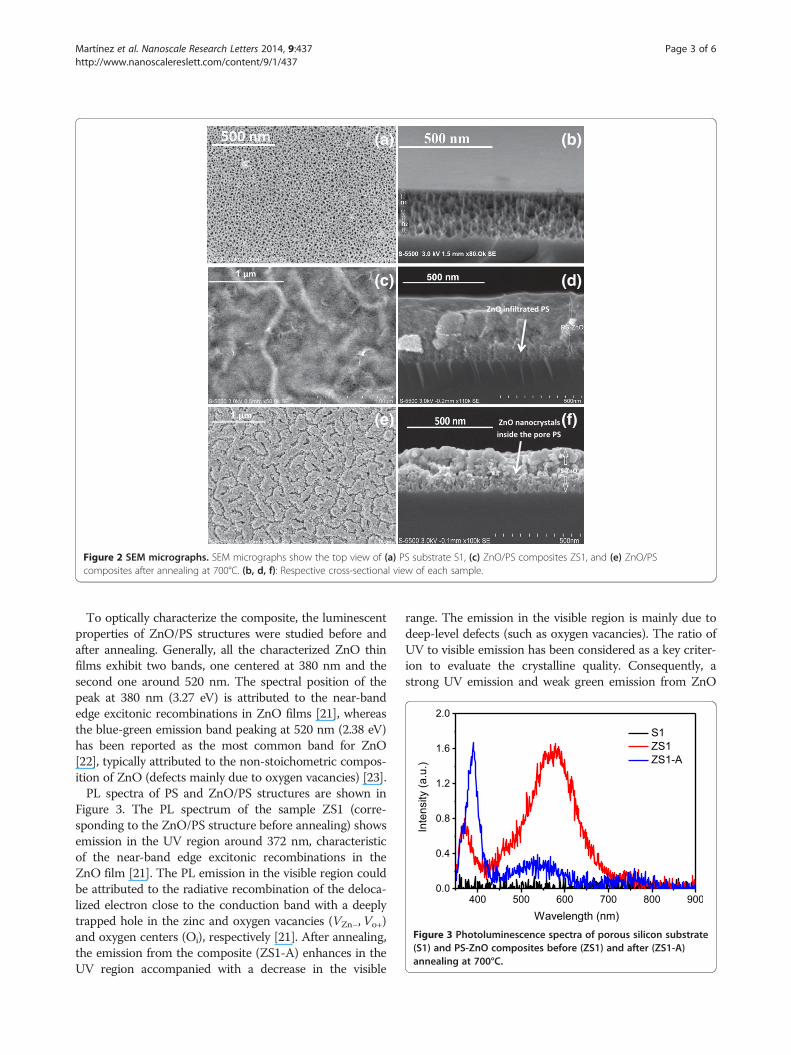
Figure 3 Photoluminescence spectra of porous silicon substrate(S1) and PS-ZnO composites before (ZS1) and after (ZS1-A)annealing at 700°C.
Martínez et al. Nanoscale Research Letters 2014, 9:437 Page 3 of 6http://www.nanoscalereslett.com/content/9/1/437
To optically characterize the composite, the luminescentproperties of ZnO/PS structures were studied before andafter annealing. Generally, all the characterized ZnO thinfilms exhibit two bands, one centered at 380 nm and thesecond one around 520 nm. The spectral position of thepeak at 380 nm (3.27 eV) is attributed to the near-bandedge excitonic recombinations in ZnO films [21], whereasthe blue-green emission band peaking at 520 nm (2.38 eV)has been reported as the most common band for ZnO[22], typically attributed to the non-stoichometric compos-ition of ZnO (defects mainly due to oxygen vacancies) [23].PL spectra of PS and ZnO/PS structures are shown in
Figure 3. The PL spectrum of the sample ZS1 (corre-sponding to the ZnO/PS structure before annealing) showsemission in the UV region around 372 nm, characteristicof the near-band edge excitonic recombinations in theZnO film [21]. The PL emission in the visible region couldbe attributed to the radiative recombination of the deloca-lized electron close to the conduction band with a deeplytrapped hole in the zinc and oxygen vacancies (VZn−,Vo+)and oxygen centers (Oi), respectively [21]. After annealing,the emission from the composite (ZS1-A) enhances in theUV region accompanied with a decrease in the visible
range. The emission in the visible region is mainly due todeep-level defects (such as oxygen vacancies). The ratio ofUV to visible emission has been considered as a key criter-ion to evaluate the crystalline quality. Consequently, astrong UV emission and weak green emission from ZnO

Martínez et al. Nanoscale Research Letters 2014, 9:437 Page 4 of 6http://www.nanoscalereslett.com/content/9/1/437
could be attributed to the good crystalline quality of theZnO film which is not the case before annealing. Thedeep-level emission is usually related to structural defectsand impurities; however, the structural defects depend onlattice mismatch [24]. The PL emission band around531 nm (2.3 eV) is associated with the radiative recombin-ation of photogenerated holes with single ionized chargeof specific defects such as oxygen vacancies or Zn intersti-tials [25-27].Figure 4a shows schematics of lateral (A) and transversal
(B) configurations of the electrodes for current-voltage(I-V) characterization. Two types of configurations (lateraland transversal) for I-V characterization were analyzed inorder to provide more information about the oxygen
Figure 4 Current-voltage (I-V) characterization. (a) Schematic of lateralover crystalline Si before and after annealing. (c) ZnO-mesoPS composite aconfigurations A (lateral) and B (transversal), respectively.
vacancies' diffusion paths. ZnO deposited on crystallinesilicon and then annealed at 700°C was also characterizedas a reference, before and after annealing (Figure 4b). Re-sults illustrated in Figure 4b reveal a simple resistor-likebehavior in both cases. Annealed ZnO-mesoPS compos-ites were tested for memristive response for both configu-rations, and the current-voltage curves of our proposeddevice after annealing (Figure 4c) reveal the zero-crossingpinched hysteresis loop characteristic of memristive de-vices [2,28] in both cases. By analyzing the results inFigure 4c, we can clearly see a better curve symmetry forthe lateral configuration (A), although some asymmetry isevident for both of them. Like a typical memristive device,the device state (Roff to Ron) remains unaffected before a
(A) and transversal (B) measurements for the same sample. (b) ZnOfter annealing. Left- and right-hand side figures correspond to the

Martínez et al. Nanoscale Research Letters 2014, 9:437 Page 5 of 6http://www.nanoscalereslett.com/content/9/1/437
certain threshold voltage. In particular, for the case of lat-eral configuration, the memristive switching ratio fromthe high resistance state (HRS) to the low resistance state(LRS) at 7 V is 1.72 for the positive bias and 3.1 for thenegative bias, which indicates a bipolar resistive switching.In the literature, there are basically two possible mech-
anisms acting in the system for the transport of oxygenvacancies, which are responsible for the demonstrationof memristive characteristics: (a) the filamentary con-ducting path [7-9] and (b) the interface-type conductingpath [7]. The first one proposes that conductive andnon-conductive zones in the oxide layers are created bythe distribution of oxygen vacancies within the materialdue to its morphology and the applied bias voltage. Thesecond one explains the resistive switching by the cre-ation of conducting filaments made of oxygen vacanciesacross the dielectric material (ZnO) under an appliedbias voltage. In the present study, the effect can be at-tributed to the fact that the use of porous silicon as asubstrate increases the effective surface area (refer toFigure 2e; granular labyrinth patterns formed on the sur-face after annealing) and hence the oxygen vacancies inZnO, which leads to the memristive behavior of thecomposite structure. Conductive channels (filamentaryconducting paths) are formed within the ZnO layer andgrain boundaries [7]. In both configurations, the pres-ence of memristive behavior suggests that a suitablegrain size can promote the diffusion of oxygen vacanciesin any direction of the device.
ConclusionsIn this paper, the ZnO-mesoPS nanocomposite is demon-strated as a potential structure in the fabrication of mem-ristive devices. Deposition of ZnO onto the mesoporoussilicon substrate and post-annealing treatment resulted inthe formation of regular labyrinth patterns with granularappearance. Mesoporous silicon as a substrate was foundto promote the modification of ZnO grain size and conse-quently a significant enhancement of oxygen vacancies,which are responsible for resistive switching. Typicalmemristive behavior is demonstrated and analyzed. Futurework is being carried out to study the tunability of the de-vice as a function of substrate porosity/morphology.
Competing interestsThe authors declare that they have no competing interests.
Authors' contributionsLM and OO carried out all the experimental work. VA and YK conceived theexperiments. All the authors analyzed and discussed the results to structureand prepare the final version of the paper. All authors read and approvedthe final manuscript.
Authors' informationLM and OO are PhD and M. Tech students, respectively, in a material scienceand technology program in a research institute (CIICAp-UAEM) in
Cuernavaca. YK is a postdoctoral fellow in UNAM. VA is working as aprofessor-scientist in CIICAp-UAEM.
AcknowledgementsThis work was financially supported by a CONACyT project (#128953). Weacknowledge the technical help provided by Jose Campos in acquiring theSEM images.
Received: 20 May 2014 Accepted: 12 August 2014Published: 27 August 2014
References1. Chua L: Memristor-the missing circuit element. Circuit Theory IEEE Transact
On 1971, 18(5):507–519.2. Strukov DB, Snider GS, Stewart DR, Williams RS: The missing memristor
found. Nature 2008, 453(7191):80–83.3. Park J, Lee S, Lee J, Yong K: A light incident angle switchable ZnO
nanorod memristor: reversible switching behavior between twonon‐volatile memory devices. Adv Mater 2013, 25(44):6423–6429.
4. Yoon SM, Warren SC, Grzybowski BA: Storage of electrical information inmetal–organic‐framework memristors. Angew Chem Int Ed 2014,53(17):4437–4441.
5. Wang ZQ, Xu HY, Li XH, Yu H, Liu YC, Zhu XJ: Synaptic learning andmemory functions achieved using oxygen ion migration/diffusion in anamorphous InGaZnO memristor. Adv Funct Mater 2012, 22(13):2759–2765.
6. Yang JJ, Pickett MD, Li X, Ohlberg DA, Stewart DR, Williams RS: Memristiveswitching mechanism for metal/oxide/metal nanodevices. NatNanotechnol 2008, 3(7):429–433.
7. Sawa A: Resistive switching in transition metal oxides. Mater Today 2008,11(6):28–36.
8. Zoolfakar AS, Kadir RA, Rani RA, Balendhran S, Liu X, Kats E, Bhargava SK,Bhaskaran M, Sriram S, Zhuiykov S, O'Mullane AP, Zadeh KK: Engineeringelectrodeposited ZnO films and their memristive switching performance.Phys Chem Chem Phys 2013, 15(25):10376–10384.
9. Liu L, Chen B, Gao B, Zhang F, Chen Y, Liu X, Kang J: Engineering oxideresistive switching materials for memristive device application. Appl PhysA 2011, 102(4):991–996.
10. Ridhuan NS, Lockman Z, Aziz AA, Khairunisak AR: Properties of ZnOnanorods arrays growth via low temperature hydrothermal reaction.Adv Mater Res 2012, 364:422–426.
11. Yao I, Tseng TY, Lin P: ZnO nanorods grown on polymer substrates as UVphotodetectors. Sensors Actuators A Phys 2012, 178:26–31.
12. Rusli NI, Tanikawa M, Mahmood MR, Yasui K, Hashim AM: Growth of high-density zinc oxide nanorods on porous silicon by thermal evaporation.Materials 2012, 5(12):2817–2832.
13. Cai F, Wang J, Yuan Z, Duan Y: Magnetic-field effect on dye-sensitizedZnO nanorods-based solar cells. J Power Sources 2012, 216:269–272.
14. Tao R, Tomita T, Wong RA, Waki K: Electrochemical and structural analysisof Al-doped ZnO nanorod arrays in dye-sensitized solar cells. J PowerSources 2012, 214:159–165.
15. Aroutiounian V, Arakelyan V, Galstyan V, Martirosyan K, Soukiassian P:Hydrogen sensor made of porous silicon and covered by TiO or ZnO Althin film. Sens J IEEE 2009, 9(1):9–12.
16. Prabakaran R, Peres M, Monteiro T, Fortunato E, Martins R, Ferreira I: Theeffects of ZnO coating on the photoluminescence properties of poroussilicon for the advanced optoelectronic devices. J Non Cryst Solids 2008,354(19):2181–2185.
17. Kumar Y, Garcia JE, Singh F, Olive-Méndez SF, Sivakumar VV, Kanjilal D,Agarwal V: Influence of mesoporous substrate morphology on thestructural, optical and electrical properties of RF sputtered ZnO layerdeposited over porous silicon nanostructure. Appl Surf Sci 2012,258(7):2283–2288.
18. Harris L, Arthur Loebal L: Evaluation and analysis of optical and electricalconstants of thin films as functions of reflectance and data by electronicdigital computation. J Opt Soc Am 1955, 45(3):179–188.
19. Monch W: On the band structure lineup of ZnO heterostructures. ApplPhys Lett 2005, 86:162101.
20. Cai H, Shen H, Yin Y, Lu L, Shen J, Tang Z: The effects of porous silicon onthe crystalline properties of ZnO thin films. J Phys Chem Solid 2009,70(6):967–971.

Martínez et al. Nanoscale Research Letters 2014, 9:437 Page 6 of 6http://www.nanoscalereslett.com/content/9/1/437
21. Wu XL, Siu GG, Fu CL, Ong HC: Photoluminescence andcathodoluminescence studies of stoichiometric and oxygen-deficientZnO films. Appl Phys Lett 2001, 78:2285–2287.
22. Djurišić AB, Leung YH: Optical properties of ZnO nanostructures. Small2006, 2(8–9):944–961.
23. Dai L, Chen XL, Wang WJ, Zhou T, Hu BQ: Growth and luminescencecharacterization of large-scale zinc oxide nanowires. J Phys CondensMatter 2003, 15(13):2221.
24. Yang CL, Wang JN, Ge WK, Guo L, Yang SH, Shen DZ: Enhanced ultravioletemission and optical properties in polyvinyl pyrrolidone surfacemodified ZnO quantum dots. J Appl Phys 2001, 90(9):4489–4493.
25. Hassan NK, Hashim MR, Mahadi MA, Allam NK: A catalyst-free growth ofZnO nanowires on Si (100) substrates: effect of substrate position onmorphological, structural and optical properties. ECS J Solid States SciTechnol 2012, 1:86–89.
26. Umar A, Kim SH, Al-Hajry A, Hahn YB: Temperature-dependantnon-catalytic growth of ultraviolet-emitting ZnO nanostructures onsilicon substrate by thermal evaporation process. J Alloys Comp 2008,463:516–521.
27. Yang JH, Zhend JH, Zahai HJ, Yang LL: Low temperature hydrothermalgrowth an optical properties of ZnO nanorods. Cryst Technol 2009,44:87–91.
28. Chew ZJ, Li L: A discrete memristor made of ZnO nanowires synthesizedon printed circuit board. Mater Lett 2013, 91:298–300.
doi:10.1186/1556-276X-9-437Cite this article as: Martínez et al.: ZnO-porous silicon nanocompositefor possible memristive device fabrication. Nanoscale Research Letters2014 9:437.
Submit your manuscript to a journal and benefi t from:
7 Convenient online submission
7 Rigorous peer review
7 Immediate publication on acceptance
7 Open access: articles freely available online
7 High visibility within the fi eld
7 Retaining the copyright to your article
Submit your next manuscript at 7 springeropen.com