SAXS and WAXS analysis of MgO doped ZnO nanostructured ceramics grown on Si and glass substrate
Upload
independentCategory
view
2download
0
Materials Research Bulletin 47 (2012) 700–707
Solution precursor plasma deposition of nanostructured CdS thin films
Raghavender Tummala, Ramesh K. Guduru *, Pravansu S. Mohanty
Department of Mechanical Engineering, University of Michigan, Dearborn, MI 48128, USA
A R T I C L E I N F O
Article history:
Received 12 September 2011
Received in revised form 11 November 2011
Accepted 19 December 2011
Available online 30 December 2011
Keywords:
A. Chalcogenides
A. Optical materials
B. Plasma deposition
C. Optical properties
D. Electrical properties
A B S T R A C T
Cadmium sulfide (CdS) films are used in solar cells, sensors and microelectronics. A variety of techniques,
such as vapor based techniques, wet chemical methods and spray pyrolysis are frequently employed to
develop adherent CdS films. In the present study, rapid deposition of CdS thin films via plasma spray
route using a solution precursor was investigated, for the first time. Solution precursor comprising
cadmium chloride, thiourea and distilled water was fed into a DC plasma jet via an axial atomizer to
create ultrafine droplets for instantaneous and accelerated thermal decomposition in the plasma plume.
The resulting molten/semi-molten ultrafine/nanoparticles of CdS eventually propel toward the substrate
to form continuous CdS films. The chemistry of the solution precursor was found to be critical in plasma
pyrolysis to control the stoichiometry and composition of the films. X-ray diffraction studies confirmed
hexagonal a-CdS structure. Surface morphology and microstructures were investigated to compare with
other synthesis techniques in terms of process mechanism and structural features. Transmission
electron microscopy studies revealed nanostructures in the atomized particulates. Optical measure-
ments indicated a decreasing transmittance in the visible light with increasing the film thickness and
band gap was calculated to be �2.5 eV. The electrical resistivity of the films (0.243 � 0.188 � 105 V cm)
was comparable with the literature values. These nanostructured polycrystalline CdS films could be useful in
sensing and solar applications.
� 2011 Elsevier Ltd. All rights reserved.
Contents lists available at SciVerse ScienceDirect
Materials Research Bulletin
jo u rn al h om ep age: ww w.els evier .c o m/lo c ate /mat res b u
1. Introduction
CdS, a metal chalcogenide semiconductor belonging to II–IVgroup, is one of the promising materials for use in variousoptoelectronic devices, light detectors, photo conductors, displaypanels, light emitting diodes and sensors [1–6]. It could also beused for photovoltaic conversion. It is preferred over other wideband gap materials for optical window applications due to itscompact crystallographic cell and electronic affinity with CuInSe2,InP, CdTe and other p-type semiconductors [7]. There is a vastliterature available reporting high efficiency solar devices of CdSwith Cu2S, Cu(InGa)Se2, and CdTe [8–10].
Usually, CdS exists in two different forms namely a-CdS(hexagonal Wurtzite) and b-CdS (cubic, zinc blend). b-CdS is ametastable phase and forms at low temperatures. a-CdS is a stablephase and forms at high temperatures, however, annealing of b-CdS can also result in the formation of a-CdS at high temperatures.For solar cell applications, hexagonal structured a-CdS films arepreferred because of stability and band gap [11]. Microstructuralfeatures, such as grain size and shape of a-CdS are very importantas they can affect the electrical properties of solar cells.
* Corresponding author. Tel.: +1 313 593 4927; fax: +1 313 593 3851.
E-mail address: [email protected] (R.K. Guduru).
0025-5408/$ – see front matter � 2011 Elsevier Ltd. All rights reserved.
doi:10.1016/j.materresbull.2011.12.018
CdS films are usually deposited by techniques like molecularbeam epitaxy (MBE) [12], metal organic chemical vapor deposition(MOCVD) [13], close-spaced sublimation (CSS) [14], electrodepo-sition [15], sputtering [16], successive ionic layer adsorption andreaction (SILAR) [17], pulsed laser deposition (PLD) [18], and spraypyrolysis [19]. Except, spray pyrolysis, all the mentionedtechniques come under bottom–up approach where the depositionof films starts either from atoms or ionic species and growthkinetics are dependent on the material transport phenomena.Vapor phase reactions for CdS formation occur at high tempera-tures [20] and low pressure conditions, as a result hexagonalstructured CdS was observed to form. Low temperature techni-ques, such as SILAR and CBD, could result in cubic phase or acombination of cubic and hexagonal structured CdS, which are notpreferred for many applications. On the other hand, spray pyrolysisis relatively faster compared to the other methods, but requiresheating of substrates above certain temperatures under regular orinert atmospheric conditions, which limits the substrate choicesthat can withstand high temperatures as well as chemicalcorrosion at high temperatures. Also, as the number of layersincreases substrate temperature needs to be increased in order toachieve right decomposition of the precursor in the top layers ofthe films. Finally, less control over the microstructures andproperties makes spray pyrolysis an unattractive process for manyapplications. In contrast to all the above discussed processing

Fig. 1. Schematic for plasma spray setup (100HE plasma gun) for solution precursor
spray.
R. Tummala et al. / Materials Research Bulletin 47 (2012) 700–707 701
methods, here a technique with solution precursor, similar to thespray pyrolysis, however, with high temperature plasma proces-sing conditions is being investigated, for the first time, to developcontinuous CdS films. In this technique, the solution precursor ispumped through high temperature plasma plume via a liquidatomizer where it thermally decomposes into molten/semi-molten nanoclusters of desired compound before depositing onthe substrate.
2. Experimental procedure
2.1. Plasma spray setup
Fig. 1 shows the plasma set-up (a modified 100HE gun,Progressive Technologies Inc., Grand Rapids, MI, USA) used forspraying CdS films from a solution precursor. The power of this guncan be varied between 35 kW and 100 kW. An axial liquid atomizerspecially designed by Mohanty et al. [21,22] was used in this gun tofeed the solution precursor into DC plasma jet. The solutionprecursor is fed with help of a peristaltic pump through apolyurethane tube. Then the precursor flows through an injectorthat holds the above mentioned liquid atomizer to atomize thesolution into fine droplets in order to facilitate for accelerated hightemperature chemical reactions. The atomized liquid droplets ofthe precursor undergo chemical reactions in the plume and turninto molten/semi-molten particles of desired compound whileexiting the plume, which are then deposited on the substrate todevelop a coating/film. Usually compressed air or Argon isemployed for atomizing the solution precursor at a pressure of140–310 kPa. To avoid back pressure from the gun, check valvesare connected to the feed ports. More details on the solutionprecursor plasma spray process can be found elsewhere [21–24].
2.2. Solution precursor and substrates
Solution precursor was prepared using cadmium chloride(CdCl2, Alfa Aesar), thiourea ((NH4)2CS, Sigma–Aldrich) and de-ionized water. CdCl2 was added to de-ionized water (400 ml) andmixed thoroughly till the complete dissolution. Then thiourea wasadded to the above solution and stirred continuously with the helpof a magnetic stirrer to form a clear solution, which was then usedin the plasma spray process. The amounts of CdCl2 and thioureaadded are shown in Table 1.
CdS was deposited on aluminum (Al) as well as glass substrates.The Al (6 cm � 5 cm � 2.5 cm, McMaster Carr.) and corning glasssubstrates (7.5 cm � 5 cm � 0.25 cm, Tedpella Inc.) were cleanedwith acetone following distilled water before deposition. Thick-ness of the films was varied on glass substrates by varying thenumber of spray cycles of plasma spray to study the variation inoptical transmission and absorbance properties of CdS as afunction of thickness.
Table 1Composition of CdS films by EDX.
Ratio between CdCl2/thiourea
in solution precursor
EDX analysis of sprayed films
Cd S
wt% at% wt%
1:1 58.50 30.4 7.24
1:2 58.89 30.47 13.62
1:3 64.93 35.73 17.82
1:5 66.64 37.07 22.99
1:8 68.60 39.08 22.82
1:10 69.56 40.11 22.65
1:15 69.79 40.34 23.00
1:20 70.03 40.57 23.29
2.3. Plasma spray parameters
Table 2 shows the optimized conditions used for spraying CdSfilms on Al and glass substrates. During plasma spray process, glasssubstrates were cooled on rear side using compressed air to avoidcracking due to thermal stresses. However, the Al substrates didnot require cooling as they were conducting the heat away tosubstrate holder while spraying the CdS films.
2.4. Characterization of CdS films
2.4.1. X-ray diffraction and X-ray photoelectron spectroscopy
Phase formation of as-sprayed films was determined by X-raydiffraction (XRD) using a Rigaku Miniflex system with a Cu Karadiation (l = 1.5405 A). The binding energies for differentelements in the films were determined from X-ray photoelectronspectroscopy (XPS) measurements carried out on Kratos axis ultraXPS. Al Ka radiation was used for the measurements at 150 W andbase pressure was 1 � 10�9 Torr. Prior to the measurements, XPSwas calibrated with Ag 3d photoelectron region.
2.4.2. Microstructural analysis
Surface morphology of the films was studied using Hitachi 2600-N scanning electron microscope (SEM) as well as atomic forcemicroscopy (AFM) (Quesant Instrument Corporation). Chemicalcomposition analysis of the films was carried out using energydispersive X-ray analyzer (EDX) on SEM. The lowest detection limitof EDX system was carbon. Microstructures of the films wasinvestigated by transmission electron microscope (TEM). Samplesfor TEM studies were prepared following drop-cast method fromscraped powders of as-sprayed films. First, the CdS films werescraped with a stainless steel knife to obtain powder particles of the
Cl Ratio (Cd:S) for at%
at% wt% at%
13.20 34.25 56.28 2.30
24.68 27.47 44.84 1.23
34.32 17.23 29.93 1.04
44.77 10.35 18.17 0.82
45.51 8.57 15.40 0.85
45.73 7.77 14.14 0.87
46.53 7.19 13.12 0.86
47.23 6.67 12.19 0.85

Table 2Solution precursor plasma spray process parameters.
Parameter Value
Power, kW (100HE) 80
Voltage, V 330
Current, A 250
Primary Gas, m3/h (Argon) 5.66
Secondary Gas, m3/h (Nitrogen) 2.83
Ternary Gas, m3/h (Hydrogen) 3.16
Standoff distance, mm 76
Feed rate, ml/min (solution precursor) 63
Atomizing gas, kPa (compressed air) 172.36
Cooling gas for glass substrates, kPa 450
No. of passes Al substrate – 25 passes
Glass substrate – 4, 8,
25 and 40 passes
605550454035302520
2theta (deg.)
Inte
ns
ity
(A
.U.)
1:1
1:2
1:3
1:5
1:8
1:10
1:15
1:20
Hexago nal CdS CdCl2 Uniden�fied phase
(CdCl2 : Th iou rea)
Fig. 2. XRD patterns for CdS films with varying ratios between CdCl2 and thiourea
(CdCl2:thiourea) in solution precursor.
R. Tummala et al. / Materials Research Bulletin 47 (2012) 700–707702
coating. These powders were suspended in methanol and sonicatedfor five minutes to attain a uniform dispersion. Droplets of sonicatedsolution were then drop-casted onto a holey carbon coated coppergrid, and subsequently heated to 80 8C to evaporate methanol. Thesesamples were then examined in JEOL 2010F TEM at differentmagnifications in conventional and dark field imaging modes as wellas diffraction mode.
2.4.3. Film thickness measurements
Thickness of the CdS films on glass substrates was measured atFilmetrics Inc., New York, USA, using FILMETRICS F20-EXR systemcoupled to a contact probe (model CP-2, spot size of �200 mm). Thecombination of contact probe, and inclusion of insulation tape onbackside of the samples produced purely ‘‘front face’’ reflectiondata. Reflectance spectra (380–1700 nm) thus obtained was thenmodeled using FILMeasure thin film fitting software to extract thefilm thickness.
2.4.4. Optical and electrical studies
Optical properties were studied in terms of percentagetransmission (%T) and absorbance (A) on CdS coated glasssubstrates using a Varian Cary 5000 spectrophotometer. Variationin absorbance and transmittance were measured as a function ofnumber of plasma spray cycles, i.e., CdS coating thickness.Electrical resistivity of CdS films was measured using a two pointcontact setup with Biologic VMP3B Analyzer. The current wasdetected while varying the voltage across the two contactterminals. The electrical measurements were done on multiplesamples on different locations of the coatings.
3. Results and discussion
3.1. Spray process and chemical analysis
Different ratios of CdCl2 and thiourea, as shown in Table 1, weremixed in the solution precursor to deposit CdS films using plasmaspray process. The concentration of CdCl2 was always kept below1 M to avoid precipitation of complexes at room temperature in thesolution precursor [25,26]. For a ratio of 1:1 between the CdCl2 andthiourea, unconverted CdCl2 and few unidentified peaks with notraces of CdS phase were detected in the X-ray diffraction (XRD)pattern of the films, see Fig. 2. For the ratios of 1:2 and 1:3, filmsshowed a mixture of CdS, CdCl2 and few other unidentified peaks.However, at higher ratios, the phases other than CdS were notdetected. At the same time, chemical composition of the filmsbased on energy dispersive X-ray (EDX) analysis indicatedpresence of Cd, S and Cl only, see Table 1. The amount of chlorinedecreased with increasing the ratio between CdCl2 and thioureawith increasing the amount of thiourea. Spray pyrolysis studies[25] showed formation of CdS without complexes only when the
process temperatures were above 300 8C. In the present case, thetemperature of plasma plume could go up to several thousands ofdegree centigrade (�10,000–12,000 8C), which is relatively veryhigh; however, the extent of accelerated chemical reactions in theplasma plume could be dependent on several factors, such aschemical composition of the precursor, time of retention for theatomized liquid droplets in the plasma plume (velocity of theplasma jet � length of the plasma plume), and vapor pressures ofthe elements involved in the chemical reaction etc. While all otherparameters were constant, except the composition of the solutionprecursor, formation of CdS with increasing the amount of thioureaindicates possible loss of sulfur during the process when theamounts of thiourea were low. According to Brown and Bates [25],and Krunks et al. [26], the solution precursor containing CdCl2 andthiourea salts in spray pyrolysis undergo different stages ofchemical reactions via various complex formation, as shown below
Cd2þðaqÞ þ 2Cl�ðaqÞ þ 2ðNH2Þ2CSðaqÞ ! CdCl2�2ðNH2Þ2CSðsÞ(1)
CdCl2�2ðNH2Þ2CSðsÞ þ 2H2O ! CdCl2�ðNH2Þ2CSðsÞ þ H2SðgÞþ CO2ðgÞ þ 2NH3ðgÞ (2)
CdC12�ðNH2Þ2CSðsÞ þ 2H2O ! CdSðsÞ þ 2HClðgÞ þ CO2ðgÞþ 2NH3ðgÞ (3)
The overall reaction is then
CdCl2ðaqÞ þ 2ðNH2Þ2CSðaqÞ þ 4H2O ! CdSðsÞ þ H2SðgÞ þ 2HClðgÞþ 2CO2ðgÞ þ 4NH3ðgÞ (4)

R. Tummala et al. / Materials Research Bulletin 47 (2012) 700–707 703
One can expect similar reactions in the solution precursorplasma spray process also, but at faster rates due to hightemperatures of the plasma plume; however, there is no evidenceto confirm the occurrence of same set of reactions in the presentstudies because of the absence of complex phases (shown in thechemical reactions) in the XRD patterns (see Fig. 2). It is also notclear, whether the high temperatures of the plasma would have ledto the formation of some unknown non-equilibrium phases duringthe process, which could not be identified in the XRD patterns.Nevertheless, small amounts of thiourea at lower ratios may haveled to either loss of sulfur or incomplete chemical reactions due tolimited availability of sulfur, and resulted in some unidentifiedphases. EDX analysis of the films showed only Cd, Cl and S withoutO, N and C. Table 1 also shows a decreasing trend in the ratiobetween Cd and S with increasing the amount of thiourea, anddecreasing amounts of chlorine, which have almost stabilizedsomewhere close to 1:10 and 1:15 ratios. With further increase inthe amount of thiourea, the ratio between Cd and S started to comedown and amount of excess sulfur increased; therefore, in the
Fig. 3. XPS spectra for CdS film.
present study, the ratio between CdCl2 and thiourea of 1:10 waschosen to deposit CdS films for further investigation. XPS studiesconducted on these films, see Fig. 3, show symmetric peaks withbinding energies for Cd (3d5/2 – 405.7 eV, full width at halfmaximum (FWHM) �1.9 eV) and S (2p3/2 – 162.12 eV) close to thereference binding energy values for CdS [27,28] and thus confirmexistence of Cd and S in the form of CdS. On the other hand, thebinding energy for Cl 2p3/2 is close to 199.2 eV, which indicatesexistence of Cl in the form of CdCl2. At the same time, the bindingenergy for Cd 3d5/2 peak is close to 405.7 eV and shows noasymmetry; however, the FWHM is slightly higher than therecommended 1.7 eV for CdS. The binding energy for Cd 3d5/2 peakis supposed to be 406.2 eV for CdCl2. Therefore, absence of clearevidence for the existence of CdCl2 may be due to very lowconcentrations, and this could be the same reason for the absenceof CdCl2 peaks in XRD patterns. The binding energy for O 1s peakwas also observed at 531.8 eV (not shown here), and it confirmspresence of CdO; however absence of oxygen peak in EDX analysisindicates possible existence of CdO only in the surface layers of theCdS films. XPS studies are also very inconclusive on the existence ofexcess sulfur either in the free form or in the lattice. Therefore,understanding the chemical reactions that occur in the plasmaplume and exact mechanism for different phase transformationsneed an in-depth investigation.
3.2. X-ray diffraction measurements
The XRD patterns obtained for a ratio of 1:10 between CdCl2 andthiourea, see Fig. 4, confirm polycrystalline nature and hexagonalcrystal structure (a = 4.138 nm, c = 6.718 nm.) of the CdS films onboth the glass and Al substrates.
3.3. Surface morphology and roughness
Fig. 5 shows the surface microstructure of CdS films depositedon Al substrate. Similar morphologies were observed for CdS filmsdeposited on the glass substrates. The inset picture in Fig. 5 showsa small splat observed on the CdS film deposited on glass substrate,which could be due to improperly atomized large droplet of thesolution precursor. Otherwise, CdS films were continuous withparticulate morphology on both the substrates. Similar surfacemorphological features were observed for the CdS films developedvia CBD [29,30], thermal evaporation [31], SILAR [32], MOCVD [33]
Fig. 4. XRD pattern for as-sprayed CdS films on corning glass and Al substrates.
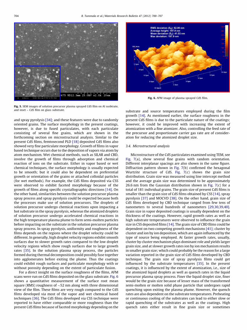
Fig. 5. SEM images of solution precursor plasma sprayed CdS film on Al susbtrate,
and inset – CdS film on glass substrate.
Fig. 6. AFM image of plasma sprayed CdS film.
R. Tummala et al. / Materials Research Bulletin 47 (2012) 700–707704
and spray pyrolysis [34]; and these features were due to randomlyoriented grains. The surface morphology in the present coatings,however, is due to fused particulates, with each particulateconsisting of several fine grains, which are shown in theforthcoming section on microstructural analysis. Similar to thepresent CdS films, femtosecond PLD [18] deposited CdS films alsoshowed very fine particulate morphology. Growth of films in vaporbased technique occurs due to the deposition of vapors via atom byatom mechanism. Wet chemical methods, such as SILAR and CBD,involve the growth of films through adsorption and chemicalreaction of ions on the substrate. Either in vapor based or wetchemical techniques, the surface morphology is usually expectedto be smooth; but it could also be dependent on preferentialgrowth or orientation of the grains or attached colloidal particles(for wet methods). For example, the CdS films deposited via CSSwere observed to exhibit faceted morphology because of thegrowth of films along specific crystallographic directions [14]. Onthe other hand, similarities between the solution precursor plasmaspray process and spray pyrolysis could be expected because boththe processes make use of solution precursors. The droplets ofsolution precursor undergo chemical reactions upon impacting ahot substrate in the spray pyrolysis, whereas the atomized dropletsof solution precursor undergo accelerated chemical reactions inthe high temperature plasma plume to form semi-molten particlesbefore impacting on the substrate in the solution precursor plasmaspray process. In spray pyrolysis, uniformity and roughness of thefilms depends on the regions where the droplet velocity could bedifferent. In generally, high droplet velocity regions exhibit smoothsurfaces due to slower growth rates compared to the low dropletvelocity regions which show rough surfaces due to large growthrates [35]. In the solution plasma spray process, the particlesformed during thermal decomposition could possibly fuse togetherinto agglomerates before exiting the plume. Thus the coatingscould exhibit rough surfaces and particulate morphology with orwithout porosity depending on the extent of particulate fusion.
For a direct insight on the surface roughness of the films, AFMscans were run on CdS films deposited on the glass substrate. Fig. 6shows a quantitative measurement of the surface root meansquare (RMS) roughness of �52 nm along with three dimensionalview of the film. These films are very rough compared to the CdSfilms developed via most of the vapor and wet chemical basedtechniques [36]. The CdS films developed via CSS technique werereported to have either comparable or more roughness than thepresent CdS films because of faceted morphology depending on the
substrate and source temperatures employed during the filmgrowth [14]. As mentioned earlier, the surface roughness in thepresent CdS films is due to the particulate nature of the coatings;however, it could be improved with increasing the extent ofatomization with a fine atomizer. Also, controlling the feed rate ofthe precursor and proportionate carrier gas rate are of consider-ation for reducing the atomized droplet size.
3.4. Microstructural analysis
Microstructure of the CdS particulates examined using TEM, seeFig. 7(a), show several fine grains with random orientation.Different interplanar spacings are also shown in the same figure.Diffraction pattern shown in Fig. 7(b) confirmed the hexagonalWurtzite structure of CdS. Fig. 7(c) shows the grain sizedistribution. Grain size was measured using line intercept methodand the average grain size was determined to be approximately26.6 nm from the Gaussian distribution shown in Fig. 7(c) for atotal of 181 individual grains. The grain size of present CdS films issmaller than the grain size of CdS films obtained by CSS [14], spraypyrolysis [37] and MOCVD [38]. On the other hand, grain size ofCdS films developed by CBD technique ranged from few tens ofnanometers to several hundreds of nanometers [29,30,39,40].Grain size in vapor deposited coatings is usually dependent on thethickness of the coatings. However, rapid growth rates as well ashigh substrate temperatures were observed to influence the grainsize in CSS deposited films [14]. The grain size of CBD films could bedependent on two competing growth mechanisms [41]; cluster bycluster and ion by ion deposition, which are again influenced by thetype of source being employed. At faster growth rates, usually,cluster by cluster mechanism plays dominant role and yields largergrain size, and at slower growth rates ion by ion mechanism resultsin smaller grain size; which could probably be the reason for a largevariation reported in the grain size of CdS films developed by CBDtechnique. The grain size of spray pyrolysis films could getinfluenced by the substrate temperatures [35]. In the presentcoatings, it is influenced by the extent of atomization, i.e., size ofthe atomized liquid droplets as well as quench rates in the liquidprecursor plasma spray process. Finer the liquid droplet size, finerwould be the grain size because of lesser mass of the transformedsemi-molten or molten solid phase particle that undergoes rapidquenching upon exiting the plasma plume. However, the quenchrates are also dependent on the substrate temperatures. Preheatingor continuous cooling of the substrates can lead to either slow orrapid quenching of the substrates as well as the coatings. Highquench rates either result in fine grain size or sometimes

Fig. 7. TEM images of CdS (a) high resolution TEM image of atomized particulate, (b)
diffraction pattern of CdS and (c) grain size distribution.
ρ =0.243 ± 0.18 8 x 10⁵ oh m-cm
0
0.01
0.02
0.03
0.04
0.05
0.06
0.07
0 0.000 5 0.00 1 0.001 5 0.00 2 0.002 5 0.00 3 0.003 5
Volta ge (V)
Curr
ent
(A)
Fig. 8. Electrical measurements of CdS – voltage (V) vs. current (I).
R. Tummala et al. / Materials Research Bulletin 47 (2012) 700–707 705
amorphous structures depending on the material being sprayed.The extent of atomization and quenching can be varied to obtaindesired grain size and microstructures in the solution precursorplasma sprayed films by varying the spray parameters.
3.5. Electrical measurements
A hemispherical probe with large area of contact was used forelectrical resistivity measurements. Fig. 8 shows an exemplarygraph obtained between current (I) and voltage (V) for the CdSfilms deposited on Al substrates. During electrical characterization,the current passed through the films was varied and then voltagewas recorded across the contact terminals. Slope of the I–V graphindicates resistance of the coating between two terminals thatmeasured the voltage across. However, using the coating thickness,which was �446.7 � 26 nm (25 spray cycles), resistivity wascalculated to be 0.243 � 0.188 � 105 V cm. Dark resistivity of presentCdS films is comparable with the resistivity of the CdS films developedvia SILAR [32] (0.419 � 105 V cm), spray pyrolysis [41,42](�105 V cm), and thermal evaporation [43] (0.01 � 105–0.818 � 105 V cm) techniques. The CdS films deposited via CBD[29,44–46] have resistivity ranging from 103 to 1010. At a giventemperature, electrical properties of CdS films are usually dependenton the grain size, imperfections (dislocations), stoichiometry anddopant or impurity concentration. Presence of CdO was also reportedto deteriorate the electrical resistivity [41]. CBD deposited films are
usually stoichiometric and may result in high resistivity [47,48]. Also,with increasing the grain size, resistivity was observed to decrease[29,32,35]. Pence et al. [19] reported an improvement in theconductivity of CdS with increasing the amount of chlorine, due toits donor activity. Cd interstitial ions or S vacancy sites also contributeto the electrical conductivity of CdS [29]. CdS films, in the presentstudies, show huge amounts of chlorine and excess sulfur (see Table1). It was uncertain whether the excess sulfur was occupying theinterstitial sites or leading to Cd vacancies in the lattice, as there wasno shift in the peaks of the XRD pattern. Similarly, chlorine may ormay not be acting as a donor in the full concentration because XRDpattern did not show additional phases or any peculiarities.Otherwise, contribution of chlorine donor and Cd vacancies togethershould result in better electrical conductivity of the CdS films, whichis not the case. According to Pence et al. [19], a concentration of1.5 � 1020 atoms/cm3 of chlorine in CdS resulted in a resistivity of90 V cm. Based on the above observations; it is very unlikely toanticipate a positive contributing effect of chlorine and Cd vacancieson the observed electrical properties of the CdS films. Therefore,segregation of excess sulfur and chlorine to the grain boundaries maybe one of the possibilities because of nanostructured grains with largeamounts of grain boundary area, which, however, needs confirma-tion. XPS studies were also very inconclusive on the existence ofexcess S and Cl either in the lattice or free form. On the other hand, thehigh resistivity of present CdS films could also be attributed to smallgrain size with possibly large amounts of residual thermal stresses inthe films, due to quenching of deposited material.
3.6. Optical properties
The absorption spectra for CdS films deposited on glasssubstrates are shown in Fig. 9. The absorbance was observed toincrease with increasing the number of spray cycles, i.e., withincreasing the thickness of CdS films. Similarly, transmittancevalues, shown in the inset of Fig. 9, have decreased with increasingthe thickness of CdS films. The transmittance of CdS films for fourspray cycles is approximately 60–80% in the visible region, which iscomparable or slightly lower than the transmittance of CdS filmsdeveloped by simplified spray using perfume atomizer [49] (75–90%), spray pyrolysis [49] (70–85%), RF magnetron sputtering [50](60–90%), solution growth technique [51] (60–85%) and CBD [52](80–90%) techniques. Absorbance of light in longer wavelengths(l � 510 nm) is usually caused by crystalline defects, such as grainboundaries and dislocations [30]. However, the absorption edge at�510 nm is due to the band gap. From solid state band theory, the

0
1
2
3
300 400 500 600 700 800
Ab
s (A
.U)
Wavelength (nm)
A - 4 pass es B - 8 passes C - 25 passes D - 40 passes
D
C
B
A
0
10
20
30
40
50
60
70
80
90
100
300 400 500 600 700 800
%T
Wavelength (nm)
A- 4 passes B -8 passes C -25 passes D -40 passes
A
B
C
D
Fig. 9. Optical properties of CdS film on glass: Variation of absorbance with respect
to number of spray cycles and inset – Variation of transmittance with respect to
number of spray cycles.
Fig. 10. Optical band gap for CdS film.
R. Tummala et al. / Materials Research Bulletin 47 (2012) 700–707706
optical band gap Eg was calculated using:
ahn ¼ Aðhn � EgÞn (5)
where A is the band edge constant, a is the absorption coefficient, h
is the Planck’s constant (6.626 � 10�34 J s), n is the frequency ofphotons (n = speed of light/wavelength of the photon), and theexponent ‘n’ characterizes the nature of band transition. The values1/2 for ‘n’ correspond to direct allowed transitions. The band gapenergy was obtained by extrapolating the straight line portion of(ahn)1/n vs. hn plot to ahn = 0. Fig. 10 shows the absorption edgedetermined by extrapolation of the linear portion of (ahn)2 line toenergy axis. The band gap of �2.5 eV was found to be independentof the film thickness and it is comparable with the literature [52].However, decrease in transmittance with increasing the coatingthickness could be attributed to rough morphology as well asincreased number of defects, such as large number of grainboundaries and particulate boundaries that can cause internalscattering of the light within the coating.
4. Conclusions
Nanostructured thin films of CdS were successfully depositedusing solution precursor plasma spray route that is capable of high
throughputs. The amount of thiourea was found to be critical in thesolution precursor to obtain CdS phase as well as to reduce theamount of residual chlorine. The CdS films obtained for a ratio of1:10 between CdCl2 and thiourea were continuous with fine grainsize in the range of few tens of nanometers. Rough morphology ofthe CdS films was due to particulate agglomerates. The electricalcharacteristics are comparable with the literature values. Howev-er, it was uncertain whether there was any contribution of excesssulfur and residual chlorine on the measured electrical properties.Also, existence of excess S and Cl in the lattice or free form isinconclusive. Decrease in transmittance with increase in the filmthickness could be due to rough morphology and increase innumber of defects, such as grain boundaries and fused particulateboundaries. The band gap of CdS films was comparable with theliterature value as well as it was observed to be independent of thefilm thickness. CdS thin films with large surface area associatedwith ultrafine particulate morphology and better transmittancecould be useful for sensor applications and optical windows forsolar cells. The solution precursor plasma spray process isadvantageous over spray pyrolysis because of rapid productionof films as well as it does not require preheating of the substrates.For example, it could be very useful for spraying films on lowmelting or polymer substrates. In addition, plasma spray processcan yield fine structures by tailoring the extent of atomization ofthe solution precursor. The solution precursor plasma sprayprocess is also scalable for large scale production of nanostructuredthin films with fine control over the microstructures.
Acknowledgments
Authors would like to thank Jarret Whetstone (Filmetrics Inc.,New York), Nagaswetha Pentyala and Elizabeth Shnerpunas (TheUniversity of Michigan, Dearborn) for thickness, electrical and AFMmeasurements of the CdS films, respectively.
References
[1] A. Henglein, Chem. Rev. 89 (1989) 1861–1873.[2] M.L. Steigerwald, L.E. Brus, Acc. Chem. Res. 23 (1990) 183–188.[3] J. Britt, C. Ferekides, Appl. Phys. Lett. 62 (1993) 2851.[4] M. Zhang, M. Drechsler, A.H.E. Muller, Chem. Mater. 16 (3) (2004) 537–543.[5] J. Kaur, D.K. Pandya, K.L. Chopra, J. Electrochem. Soc. 127 (1980) 943.[6] P.J. Sebastian, M. Ocampo, Sol. Energy Mater. Sol. Cells 44 (1996) 1–10.[7] O. Savadogo, Sol. Energy Mater. Sol. Cells 52 (1998) 361.[8] J.P. Ge, Y.D. Li, Adv. Funct. Mater. 14 (2004) 157–162.[9] M. Uekita, K.F. Nelson, C.W. Bates Jr., J.B. Mooney, J.M. Recktenwald, Thin Solid
Films 88 (1982) 275–278.[10] R.B. Hall, J.D. Meakin, Thin Solid Films 63 (1979) 203–211.[11] J. Hedstrom, H. Ohlsen, M. Bodegard, A. Kylner, L. Stolt, D. Hariskos, M. Ruckh,
H.-W. Schock, Proc. 23rd IEEE PVSC, 1993, p. 364.[12] W.G. Wilke, R. Seedorf, K. Horn, J. Vac. Sci. Technol. B 7 (1989) 807.[13] P. O’Brien, R. Nomura, J. Mater. Chem. 5 (1995) 1761–1773.[14] A.I. Oliva, R. Castro-Rodrıguez, O. Solıs-Canto, V. Sosa, P. Quintana, J.L. Pena, Appl.
Surf. Sci. 205 (2003) 56–64.[15] T. Torimoto, S. Nagakubo, M. Nishizawa, H. Yoneyama, Langmuir 25 (1998)
7077–7081.[16] H. Hernandez-Contreras, C. Mejıa-Garcıa, G. Contreras-Puente., Thin Solid Films
451 (452) (2004) 203–206.[17] G. Larramona, C. Chone, A. Jacob, D. Sakakura, B. Delatouche, D. Pere, X. Cieren, M.
Nagino, R. Bayon, Chem. Mater. 18 (6) (2006) 1688–1696.[18] M. Sanz, R. de Nalda, J.F. Marco, J.G. Izquierdo, L. Banares, M. Castillejo, J. Phys.
Chem. C 114 (11) (2010) 4864–4868.[19] S. Pence, E. Varner, C.W. Bates Jr., Mater. Lett. 23 (1995) 13–16.[20] R.E. Aitchison, Nature 167 (1951) 812–813.[21] P. Mohanty, N.A. Moroz, The University of Michigan, Patent # 12/722,342, filed
May 3, 2010.[22] N.A. Moroz, H. Umapathy, P. Mohanty, J. Therm. Spray Technol. 19 (2010)
294–302.[23] L. Xie, X. Ma, E.H. Jordan, N.P. Padture, D.T. Xiao, M. Gell, Mater. Sci. Eng. A 362
(2003) 204–212.[24] J. Karthikeyan, C.C. Berndt, J. Tikkanen, J.Y. Wang, A.H. King, H. Herman, Nanos-
truct. Mater. 9 (1997) 137–140.[25] B.J. Brown, C.W. Bates Jr., Thin Solid Films 188 (1990) 301–305.[26] M. Krunks, E. Mellikov, E. Sork, Thin Solid Films 145 (1986) 105–109.[27] M. Stoev, A. Katerski, J. Mater. Chem. 6 (3) (1996) 377–380.

R. Tummala et al. / Materials Research Bulletin 47 (2012) 700–707 707
[28] S. Kolhe, S.K. Kulkarni, A.S. Nigavekar, V.G. Bhide, J. Mater. Sci. 22 (1987)1067–1080.
[29] H. Khallaf, I.O. Oladeji, G. Chai, L. Chow, Thin Solid Films 516 (2008) 7306–7312.[30] J.Y. Choi, K.-J. Kim, J.-B. Yoo, D. Kim, Sol. Energy 64 (1998) 41–47.[31] U. Pal, R. Silva-Gonzfilez, G. Martfnez-Montes, M. Gracia-Jimenez, M.A. Vidal, Sh.
Torres, Thin Solid Films 305 (1997) 345–350.[32] B.R. Sankapal, R.S. Mane, C.D. Lokhande, Mater. Res. Bull. 35 (2000) 177–184.[33] M. Tsuji, T. Aramoto, H. Ohyama, T. Hibino, K. Omura, J. Cryst. Growth 214/215
(2000) 1142–1147.[34] S. Pence, C.W. Bates Jr., L. Varner, Mater. Lett. 23 (1995) 195–201.[35] D.S. Albin, S.H. Risbud, Thin Solid Films 147 (1987) 203–212.[36] K.K. Nanda, S.N. Sahu, Appl. Surf. Sci. 119 (1997) 50–54.[37] A.A. Yadav, M.A. Barote, E.U. Masumdar, Solid State Sci. 12 (2010) 1173–1177.[38] H. Uda, H. Yonezawa, Y. Ohtsubo, M. Kosaka, H. Sonomura, Sol. Energy Mater. Sol.
Cells 75 (2003) 219–226.
[39] D.S. Boyle, P. O’Brien, D.J. Otway, O. Robbe, J. Mater. Chem. 9 (1999) 725–729.[40] L. Wan, Z. Bai, Z. Hou, D. Wang, H. Sun, L. Xiong, Thin Solid Films 518 (2010)
6858–6865.[41] D. Chaa, S. Kim, N.K. Huang, Mater. Sci. Eng. B 106 (2004) 63–68.[42] N. Golovan, V. Smyntyna, Sens. Actuators B 6 (1992) 289–292.[43] A. Ashour, N. El-Kadry, S.A. Mahmoud, Thin Solid Films 269 (1995) 117–120.[44] H. Oumous, H. Hadiri, Thin Solid Films 386 (2001) 87–90.[45] J.P. Enrıquez, X. Mathew, Sol. Energy Mater. Sol. Cells 76 (2003) 313–322.[46] H. Metina, R. Esen, J. Cryst. Growth 258 (2003) 141–148.[47] O. Vigil, O. Zeleya-Angel, Y. Rodriguez, Semicond. Sci. Technol. 15 (2000) 259.[48] P.K. Nair, P. Parmananda, M.T.S. Nair, J. Cryst. Growth 206 (1999) 68.[49] K. Ravichandran, P. Philominathan, Appl. Surf. Sci. 255 (2009) 5736–5741.[50] J.H. Lee, D.J. Lee, Thin Solid Films 515 (2007) 6055–6059.[51] I. Yu, T. Isobe, M. Senna, Mater. Res. Bull. 30 (1995) 975–980.[52] V. Popescu, E.M. Pica, I. Pop, R. Grecu, Thin solid films 349 (1999) 67–70.
Copyright © 2022 FDOKUMEN