Graphene-modified nanostructured vanadium pentoxide ... - Nature
Upload
khangminh22Category
view
3download
0
The University of Nottingham
School of Physics & Astronomy
Optical properties of nanostructured
semiconductors grown by MBE on
non-conventional GaAs substrates
by
ALMONTASER BELLAH FATHY KHATAB
Thesis submitted to the University of Nottingham
for the degree of Doctor of Philosophy
February 2014
i
ABSTRACT
This thesis reports the optical properties of InAlAs QDs and InGaAsN QWs grown
by Molecular Beam Epitaxy (MBE) on both the conventional (100) and high Miller
index surfaces.
InAlAs QDs on AlGaAs matrix are grown by MBE on the conventional (100)
and non-(100) GaAs substrates using different growth conditions, namely, growth
temperature, different confinement barriers, and amount of deposited material. PL
measurements revealed differences in the optical properties that are caused by
substrate orientation effects. The PL emission energies of QDs grown on high Miller
index surfaces such as (311)A and (311)B are found to be strongly dependent on the
atomic terminated surface [A (Ga face) or B (As face)] of the substrate. The QDs
grown on (311)B plane show superior optical properties over QDs grown on (311)A
and (100) planes. The optimum structure to achieve the highest optical efficiency of
QDs emitting in the visible red part of electromagnetic spectrum ( 666 nm)
consisted of 4.4MLs Al0.35In0.65As/Al0.45Ga0.55As QDs grown on (311)B plane at a
growth temperature of 550 0C.
In addition, a further investigation was carried out to study the effect of post-
growth thermal annealing on the optical properties of InAlAs QDs grown on (100),
(311)A, and (311)B planes. A noticeable enhancement of the PL intensity at 10 K for
all planes was observed by increasing the annealing temperature up to 700 0C.
Thermal annealing of (311)A InAlAs/GaAlAs QDs resulted in a negligible blue
shift, while a large blue shift was observed from (311)B and (100) QDs. This is
explained by the smaller size of QDs, smaller strain, and lower In segregation from
(311)A GaAs orientation.
PL and Transmission Electron Microscopy (TEM) have been used to investigate the
optical and structural properties, respectively, of In0.36Ga0.64As1-yNy/GaAs double
quantum wells (QWs) grown both on the conventional (100) and non-(100) GaAs
substrates. These include In0.36Ga0.64As1-yNy/GaAs QWs with three different
compositions of nitrogen, namely, 0%, 1%, and 2%.
QWs grown on (311)A GaAs plane show higher nitrogen incorporation over all the
other planes. TEM measurements show that (311)B QWs have inferior structural

ii
properties than QWs grown on (311)A and (100). TEM images demonstrated that
the (311)B QWs interfaces are undulated and not uniform. In contrast QWs grown
on (311)A and (100) display very uniform and very flat interfaces.
The effect of thermal annealing on the optical properties of In0.36Ga0.64As1-yNy/GaAs
double QWs grown on different planes was investigated for two sets of samples
having 0% and 1% nitrogen. It was found that annealing at 700 0C for 30 seconds is
the optimum annealing temperature which improves the PL efficiency for all QWs.
The PL enhancement is larger in samples with 1% nitrogen than 0%.

iii
PUBLICATIONS AND CONFERENCE
PRESENTATIONS
1) A. Khatab, M. Shafi, R. H. Mari, M. Aziz, M. Henini, G. Patriarche, D. Troadec,
M. Sadeghi, and S. Wang, Comparative Optical Studies of InGaAs/GaAs
Quantum Wells Grown by MBE on (100) and (311)A GaAs planes, Physica
Status Solidi (c), 9(7), 1621 (2012).
2) Poster presentation at Semiconducting and Insulating Materials Conference
(SIMC- XVI), held at the KTH, Kista-Stokholm, Sweden, June 20-23, (2011),
Comparative optical studies of InGaAs/GaAs quantum wells grown by MBE on
(100) and (311)A GaAs plane
Work not included in the thesis:
3) A. J. Ramsay, S. J. Boyle, T. M. Godden, R. S. Kolodka, A. F. A. Khatab, J. B.
Oliveira, J. Skiba-Szymanska, H. Y. Liu, M. Hopkinson, A. M. Fox, and M. S.
Skolnick, Towards Coherent Optical Control of a Single Hole Spin: Rabi
Rotation of a Trion Conditional on the Spin State of the Hole, Solid State
Communications, 149, 1458 (2009).
4) A. F. A. Khatab, A. J. Ramsay, S. J. Boyle, A. M. Fox, and M. S. Skolnick,
Inversion Recovery Measurements of Exciton Fine-Structure Beats in a Single
Quantum Dot, Journal of Physics: Conference Series 245, 012010 (2010).
5) M. Shafi, R. H. Mari, A. Khatab, D. Taylor, and M. Henini, Deep-level Transient
Spectroscopy of GaAs/AlGaAs Multi-Quantum Wells Grown on (100) and
(311)B GaAs Substrates, Nanoscale Research Letters, 5, 1948 (2010).
6) R. H. Mari, Muhammad Shafi, Mohsin Aziz, Almontaser Khatab, David Taylor,
and Mohamed Henini, Electrical Characterisation of Deep Level Defects in Be-
iv
doped AlGaAs grown on (100) and (311)A GaAs substrates by MBE, Nanoscale
Research Letters 6,180 (2011).
7) D. L. Sales, E. Guerrero, J. F. Rodrigo, P. L. Galindo, A. Yáñez, M. Shafi, A.
Khatab, R. H. Mari, M. Henini, S. Novikov, M. F. Chisholmand, and S. I.
Molina, Distribution of Bismuth Atoms in Epitaxial GaAsBi, Applied Physics
Letters, 98, 101902 (2011).
8) M. Shafi, R. H. Mari, A. Khatab, M. Henini, A. Polimeni, M. Capizzi, and M.
Hopkinson, Deep levels in H-irradiated GaAs1-xNx (x < 0.01) grown by
Molecular Beam Epitaxy, Journal of Applied Physics, 110, 124508 (2011).
9) O. M. Lemine, M. Bououdina, M. Sajieddine, A. M. Al-Saie, M. Shafi, A.
Khatab, M. Al-hilali, and M. Henini, Synthesis, Structural, Magnetic and Optical
Properties of Nanocrystalline ZnFe2O4, Physica B, 406, 1989 (2011).
10) M. Ayvacikli, A. Khatab, A. Ege, I. Sabikoglu, M. Henini, and N. Can,
Absorption and Photoluminescence Spectroscopy of Er3+
-Doped SrAl2O4
Ceramic Phosphors, Philosophical Magazine Letters, 92(4), 194 (2012).
11) S. U. Satilmis, A. Ege, M. Ayvacikli, A. Khatab, E. Ekdal, E. J. Popovici,
M. Henini, and N. Can, Luminescence Characterization of Cerium Doped
Yttrium Gadolinium Aluminate Phosphors, Optical Materials, 34, 1921 (2012).
12) R. H. Mari, M. Aziz, M. Shafi, A. Khatab, D. Taylor, and M. Henini, Effect of
Epitaxial Layer Thickness on the Deep level Defects in MBE Grown n-Type
Al0.33Ga0.67As, Physica Status Solidi (C), 9 (7), 1643 (2012).
13) M. Ayvacikli, Z. Kotan, E. Ekdal, Y. Karabulut, A. Canimoglu, J. GarciaGuinea,
A. Khatab, M. Henini, and N. Can, Solid State Synthesis of SrAl2O4: Mn2+
Co-
doped with Nd3+
Phosphor and its Optical Properties, Journal of Luminescence
144, 128 (2013).

v
14) A. Khatab, O. M. Lemine, A. Alkaoud, A. Falamas, M. Aziz, Y. Galvão
Gobatod, M. Henini, Photoluminescence Intensity Enhancement in Self-
Assembled InAs Quantum Dots Grown on (311)B, and (100) GaAs Substrates
and Coated with Gold Nanoparticles, physica E, 54, 233 (2013).
15) M. Aziz, P. Ferrandis, A. Mesli, R. H. Mari, J. F. Felix, A. Sellai, D. Jameel, N.
Al Saqri, A. khatab, D. Taylor, M. Henini, Deep-level Transient Spectroscopy of
Interfacial States in “Buffer-Free” p-i-n GaSb/GaAs Devices, Journal Of Applied
Physics 114, 134507 (2013).

vi
ACKNOWLEDGEMENTS
“All praise is due to Allah, the Lord of the Worlds”.
First and foremost, I would like to acknowledge and express my deepest gratitude to
my supervisor Prof. M. Henini for numerous opportunities he made possible to me
during my PhD; from conferences to collaborations. Many thanks for always having
faith in my work. I have been a very privileged student.
I would like to thank Dr. David Scurr from School of Pharmacy, Nottingham
University for helping with SIMS measurements and analysis. Specials thanks to Mr
David Taylor for his assistance in processing, Robert Chettle for electronic
support.
I am also grateful to Prof Yara Gobato, Universidade Federal de São Carlos, Brazil,
for the useful discussions on the PL data.
I would like to thank all my collaborators; Dr M. Sadeghi, and Prof S. Wang in
Photonics Laboratory, Department of Microtechnology and Nanoscience, Chalmers
University of Technology, Sweden, for providing me with nitrogen quantum well
samples; Drs G. Patriarche and D. Troadec from CNRS ((France) for TEM
characterization.
I would like to thank Dr M. Shafi, Dr. Riaz Mari and Mr Mohsin Aziz for their
support and friendship.
The financial support of University of Cairo, and higher ministry of Education,
Egypt is very much appreciated.
Most importantly, thanks to my mother, my beloved wife, my uncle (Ibrhaim) and
my whole family for their love and support. Finally, I would like to dedicate this
work to the late father.

vii
TABLE OF CONTENTS
CHAPTER 1: INTRODUCTION ............................................................................... 1
1.1 INTRODUCTION ................................................................................................. 2
1.2 InAlAs QUANTUM DOTS .................................................................................. 3
1.3 DILUTE NITRIDE III-V ALLOYS (InGaAsN) ................................................... 4
1.4 ORGANIZATION OF THE THESIS .................................................................... 6
REFERENCES ............................................................................................................. 8
CHAPTER 2: FUNDAMENTAL CONCEPTS OF SEMICONDUCTORS ........... 11
2.1 INTRODUCTION ............................................................................................... 12
2.2 INTRINSIC AND EXTRINSIC SEMICONDUCTORS ..................................... 14
2.3 CRYSTAL STRUCTURE OF SEMICONDUCTORS ....................................... 16
2.3.1 Basic Lattice Types ....................................................................................... 17
2.3.2 The Reciprocal Lattice and Miller Indices .................................................... 21
2.3.3 Conventional and Non-Conventional Plane .................................................. 24
2.4 ENERGY BAND GAP ........................................................................................ 28
2.5 DIRECT AND INDIRECT BAND GAP SEMICONDUCTOR ......................... 30
2.6 TEMPERATURE DEPENDENCE OF THE ENERGY BAND GAP ................ 31
2.7 BAND STRUCTURE MODIFICATION ............................................................ 33
2.7.1 Alloys ............................................................................................................ 33
2.7.2 Heterostructures ............................................................................................. 36
2.7.2.1 Type I Band Alignment .......................................................................... 37
2.7.2.2 Type II Band Alignment ......................................................................... 37
2.7.2.3 Type III Band Alignment ........................................................................ 37
2.7.2.4 Anderson’s rule ....................................................................................... 38
2.8 PROPERTIES OF SELECTED SEMICONDUCTOR MATERIALS ................ 40

viii
2.8.1 Gallium Arsenide (GaAs) .............................................................................. 40
2.8.2 Aluminium Gallium Arsenide (AlGaAs) ...................................................... 42
2.8.3 Dilute Nitride Alloys ..................................................................................... 45
2.8.3.1 GaAsN Alloy .............................................................................................. 47
2.8.3.2 GaInAsN Alloy .......................................................................................... 48
2.9 OPTICAL PROPERTIES OF SEMICONDUCTORS......................................... 48
2. 9.1 Absorption Processes ................................................................................... 49
2.9.2 Photoluminescence ........................................................................................ 52
REFERENCES ........................................................................................................... 57
CHAPTER 3: THE GROWTH AND OPTICAL PROPERTIES OF LOW
DIMENSIONAL SEMICONDUCTOR STRUCTURES .......................................... 63
3.1 INTRODUCTION ............................................................................................... 64
3.2 QUANTUM CONFINEMENT ............................................................................ 65
3.3 DENSITY OF STATES ....................................................................................... 66
3.4 OPTICAL PROCESSES IN LOW DIMENSIONAL SEMICONDUCTOR
STRUCTURES .......................................................................................................... 68
3.4.1 ABSORPTION IN SEMICONDUCTOR NANOSTRUCTURES ............... 68
3.4.2 PHOTOLUMINESCENCE PROCESS IN NANOSTRUCTURES ............. 71
3.5 EPITAXIAL GROWTH OF LOW DIMENSIONAL SEMICONDUCTOR
STRUCTURES .......................................................................................................... 73
3.5.1 MOLECULAR BEAM EPITAXY ............................................................... 73
3.5.2 GROWTH OF QUANTUM WELL STRUCTURES ................................... 74
3.5.3 GROWTH OF QUANTUM WIRES ............................................................ 77
3.5.3 GROWTH OF QUANTUM DOTS .............................................................. 79
3.6 CARRIER DYNAMICS IN LOW DIMENSIONAL SEMICONDUCTOR
STRUCTURES .......................................................................................................... 83
REFERENCES ........................................................................................................... 85
CHAPTER 4: EXPERIMENTAL TECHNIQUES .................................................. 86

ix
4.1 PHOTOLUMINESCENCE ................................................................................. 87
4.1.1 SYSTEM HARDWARE IMPLEMENTATION ........................................ 89
4.1.1.1 SPECTROMETER ................................................................................. 89
4.1.1.2 LASERS, LIGHT CHOPPER AND OPTICS ........................................ 89
4.1.1.3 DETECTORS ......................................................................................... 91
4.1.1.4 SPECTRACQ2 ....................................................................................... 91
4.1.1.5 LOCK-IN AMPLIFIER .......................................................................... 91
4.1.1.6 CRYOSTAT AND TEMPERATURE CONTROLLER ........................ 92
4.1.1.7 COMPUTER INTERFACE .................................................................... 92
4.1.1.8 SYSTEM CONTROLLING SOFTWARE ............................................. 93
4.2 STRUCTURAL CHARACTERIZATION .......................................................... 93
4.2.1 ELECTRON MICROSCOPY ....................................................................... 93
4.2.2 TEM INSTRUMENTATION ....................................................................... 95
4.3 TIME OF FLIGHT SECONDARY ION MASS SPECTROMETRY ................. 96
4.3.1 INTRODUCTION TO SECONDARY ION MASS SPECTROMETRY
(SIMS) .................................................................................................................... 96
4.3.2 THEORY OF TOF-SIMS OPERATION ...................................................... 97
4.3.3 MODES OF ANALYSIS USING TOF-SIMS .............................................. 98
4.3.4 TOF-SIMS INSTRUMENTATION .............................................................. 99
REFERENCES ......................................................................................................... 101
CHAPTER 5: OPTICAL PROPERTIES OF SELF-ASSEMBLED InAlAs/AlGaAs
QDs GROWN BY MBE ON DIFFERENT GaAs SUBSTRATE ORIENTATIONS102
5.1 INTRODUCTION ............................................................................................. 103
5.2 EXPERIMENTAL RESULTS AND ANALYSIS ............................................ 106
5.2.1 STUDY OF THE INFLUENCE OF THE SUBSTRATE ORIENTATION
ON THE OPTICAL PROPERTIES OF Al0.35In0.65As/Al0.45Ga0.55As QUANTUM
DOTS .................................................................................................................... 107

x
5.2.2 EFFECT OF INCREASING DEPOSITED InAlAs MATERIAL ON THE
OPTICAL PROPERTIES OF QUANTUM DOTS GROWN ON DIFFERENT
SUBSTRATE ORIENTATIONS. ........................................................................ 119
5.3 EFFECT OF THE AlGaAs CARRIER CONFINING POTENTIAL ON THE
EMISSION ENERGY OF (311)B QDS .................................................................. 125
5.3.1 INTRODUCTION ....................................................................................... 125
5.3.2 EXPERIMENTAL RESULTS AND ANALYSIS ...................................... 126
5.4 EFFECT OF GROWTH TEMPERATURE ON OPTICAL EFFICIENCY OF
(311)B InAlAs QDs GROWN ON Al0.45Ga0.55As MATRIX .................................. 132
5.5 CONCLUSION .................................................................................................. 135
REFERENCES ......................................................................................................... 136
CHAPTER 6: ANNEALING EFFECT ON InAlAs QUANTUM DOTS GROWN
ON (100), (311)A, (311)B GaAs SUBSTRATES ................................................... 142
6.1 INTRODUCTION ............................................................................................. 143
6.2 EXPERIMENTAL RESULTS AND ANALYSIS ............................................ 148
6.2.1 LOW TEMPERATURE PHOTOLUMINESCENCE OF ANNEALED
SAMPLES AT DIFFERENT TEMPERATURES ............................................... 149
6.2.2 TEMPERATURE DEPENDENCE OF PHOTOLUMINESCENCE: A
COMPARISON BETWEEN AS-GROWN AND ANNEALED InAlAs QDs .... 154
6.3 CONCLUSION .................................................................................................. 163
REFRENCES ........................................................................................................... 164
CHAPTER 7: OPTICAL PROPERTIES OF Ga1-xInxNyAs1-y/GaAs DOUBLE
QUANTUM WELL STRUCTURES GROWN ON (100), (311)A, and (311)B GaAs
SUBSTRATES ......................................................................................................... 168
7.1 INTRODUCTION ............................................................................................. 169
7.2 LITERATURE REVIEW OF EPITAXIAL GROWTH OF GaInNAs ON (100)
AND HIGH INDEX GaAs SUBSTRATES ............................................................ 170
7.3 EXPERIMENTAL RESULTS AND ANALYSIS ............................................ 174

xi
7.3.1 STUDY OF THE INFLUENCE OF THE SUBSTRATE ORIENTATION
ON THE OPTICAL PROPERTIES OF In0.36Ga0.64As1-1-yNy/GaAs QUANTUM
WELLS GROWN BY MBE ON (100), (311)A AND (311)B GaAs PLANES. . 174
7.3.2 CORRELATION BETWEEN TRANSMISSION ELECTRON
MICROSCOPY IMAGES AND FULL WIDTH AT HALF MAXIMUM OF PL
SPECTA OF In0.36Ga0.64As0.99N0.01/GaAs DOUBLE QUANTUM WELLS. ...... 181
7.3.3 TEMPERATURE DEPENDENCE OF PHOTOLUMINESCENCE: A
COMPARISON AMONG In0.36Ga0.64As1-yNy/GaAs DOUBLE QWs GROWN ON
DIFFERENT SUBSTRATES WITH DIFFERENT NITROGEN PERCENTAGE.186
7.3.3.1 INTRODUCTION AND LITERATURE REVIEW OF
TEMPERATURE DEPENDENCE OF PL FOR InGaAs1-yNy/GaAs QWs. .... 186
7.3.3.2 EXPERIMENTAL RESULTS ............................................................. 187
7.4 CONCLUSION .................................................................................................. 199
REFRENCES ........................................................................................................... 200
CHAPTER 8: POST GROWTH ANNEALING OF Ga1-xInxNyAs1-y/GaAs
DOUBLE QUANTUM WELL STRUCTURES GROWN ON (100), (311)A, and
(311)B GaAs SUBSTRATES .................................................................................. 204
8.1 INTRODUCTION ............................................................................................. 205
8.2 EXPERIMENTAL RESULTS AND ANALYSIS ............................................ 207
8.2.1 PHOTOLUMINESCENCE OF ANNEALED Ga1-xInxAs/GaAs DQWs
SAMPLES AT DIFFERENT TEMPERATURES ............................................... 209
8.2.2 PHOTOLUMINESCENCE OF ANNEALED Ga1-xInxNyAs1-y/GaAs DQWs
SAMPLES AT DIFFERENT TEMPERATURES ............................................... 213
8.3 SIMS OF AS-GROWN and ANNEALED Ga0.64In0.36N0.1As0.99/GaAs DQWs
SAMPLES AT DIFFERENT TEMPERATURES .................................................. 217
8.4 CONCLUSION .................................................................................................. 222
REFERENCES ......................................................................................................... 223
CHAPTER 9: CONCLUSION AND FUTURE WORK ........................................ 226
9.1 CONCLUSION .................................................................................................. 227

xii
9.1.1 InAlAs QUANTUM DOTS ........................................................................ 227
9.1.2 InGaAsN QUANTUM WELLS .................................................................. 229
9.2 SUGGESTIONS FOR FUTURE WORK .......................................................... 230
REFERENCES ......................................................................................................... 232

xiii
LIST OF FIGURES
Figure 1.1: Band gap versus lattice constant for various III-V alloys. ....................... 5
Figure 2.1: intrinsic and extrinsic silicon. ................................................................. 16
Figure 2.2: The formation of the crystal structure from the combination of lattice
and basis is shown. The basis may consist of one atom (A) or group of atoms (B). . 17
Figure 2.3: A simple cubic lattice showing the primitive vectors. The crystal is
produced by repeating the cubic cell through space. ................................................. 18
Figure 2.4: The body centred cubic lattice along with a choice of primitive vectors.18
Figure 2.5: Primitive basis vectors for the face centered cubic lattice. .................... 19
Figure 2.6: The zinc blende crystal structure consists of the interpenetrating fcc
lattices, one displaced from the other by a distance , ,4 4 4
a a a
along the body
diagonal. The underlying Bravais lattice is fcc with a two atoms basis. The positions
of the two atoms is (000) and , , .4 4 4
a a a
.................................................................. 20
Figure 2.7: Miller indices of some important planes in a cubic crystal. ................... 23
Figure 2.8: illustration of (100) plane and non-100 planes (tilted or high index
planes). The black and white circles represent group V and group III atoms,
respectively. ............................................................................................................... 25
Figure 2.9: (211)B GaAs viewed along the (011) direction. The heavy line
highlights the (100) terrace structure. ........................................................................ 26
Figure 2.10: (311)B GaAs viewed along the (011) direction. The heavy line
highlights the (100) terrace structure16
. ...................................................................... 27
Figure 2.11: (511)B GaAs viewed along the (011) direction. The heavy line
highlights the (100) terrace structure16
....................................................................... 27
Figure 2.12: simplified energy–band structures of semiconductors. ........................ 29
Figure 2.13: energy band structures of direct semiconductor (left) and indirect
semiconductor (right). ................................................................................................ 31
Figure 2.14: energy band gap as a function of temperature of GaAs, Si, and Ge .... 32

xiv
Figure 2.15: Band gap energy versus lattice constant of various III-V
semiconductors at room Temperature. ....................................................................... 34
Figure 2.16: A schematic example of (a) a clustered, (b) an ordered, and (c) a
random alloy............................................................................................................... 35
Figure 2.17: Lattice constant as a function of composition for ternary III-V
semiconductors. All cases obey Vegard’s law. The dashed lines show regions where
miscibility gaps are expected29
................................................................................... 36
Figure 2.18: Classification of heterojunctions according to their band alignment,
where EC, EV, Eg, ΔEC, and ΔEV are the conduction band, valence band, energy gap,
conduction band offset, and valence band of the materials, respectively. ................. 38
Figure 2.19: Band diagram of (a) two separated semiconductors and (b) two
semiconductors in contact. The semiconductors have a band gap energy g
AE and
g
BE and an electron affinity of A and B . ............................................................ 39
Figure 2.20: Conventional unit cube for GaAs. ........................................................ 41
Figure 2.21: Diagram of the band structure in the vicinity of the energy gap of
GaAs: (a) throughout the first Brillouin zone, (b) a magnified view near the zone
center. ......................................................................................................................... 42
Figure 2.22: Variation of the conduction band valleys in AlxGa1-xAs as a function of
Al composition (x) at 300 K....................................................................................... 43
Figure 2.23: Schematic diagram of band anticrossing model of GaAsN. Solid lines:
calculated dispersion relation for E± subbands of GaAs1-xNx using BAC model.
Dotted lines: unperturbed energies of the N level (EN) and the GaAs conduction
band. ........................................................................................................................... 47
Figure 2.24: Interband optical absorption between an initial state of energy Ei in an
occupied lower band and a final state at energy Ef in an upper band. The energy
difference between the two bands is Eg. .................................................................... 50
Figure 2.25: absorption coefficient as a function of energy of incident light of GaAs
and silicon near their band edges. Note that the vertical axis is logarithmic. ............ 51
Figure 2.26: Photoluminescence in a solid. Incoming photons with energy higher
than the band gap energy excite an electron from ground state to excited state.
Electron relaxes to the lowest available level before dropping down to empty levels
in the ground state band by emitting a photon. .......................................................... 53

xv
Figure 2.27: Absorption,and spontaneous emission transitions between two levels
of an atom in the presence of electromagnetic radiation............................................ 55
Figure 3.1: Density of states N(E) in the conduction band for (a) bulk semiconductor
(3D), (b) quantum well (2D), (c) quantum wire (1D), and quantum dot (0D)........... 68
Figure 3.2: Low-temperature absorption spectrum of a 40-period GaAs/AlAs
multiple quantum well structure with 7.6 nm wide wells. The most intense features
result from transitions between the nth
(n = 1, 2, 3) confined light hole (lh) and heavy
(hh) hole states and identical index electron states. In addition, two weaker
transitions are observed between electron states (e1 and e3) and the first (hh1) and
third heavy hole (hh3) states, namely hh3 - e1 and hh1 - e3. .................................... 70
Figure 3.3: Room temperature absorption spectrum of a GaAs/Al0.28Ga0.72As MQW
structure containing 77 GaAs quantum wells of width 10 nm. The absorption
spectrum of bulk GaAs at the same temperature is shown for comparison. .............. 70
Figure 3.4: Emission spectrum of a quantum well structure containing five wells of
different thicknesses. The wells are Ga0.47In0.53As and the barriers are InP. The inset
shows the electronic structure and the nature of the optical transitions. .................... 71
Figure 3.5: Emission spectra of an ensemble of InAs self-assembled quantum dots
for three different laser power densities. At the highest power, emission from three
different transitions is observed. The numbers by each spectrum indicate the relative
intensity scale factors ................................................................................................. 72
Figure 3.6: (a) Schematic diagram of a single GaAs/A1GaAs quantum well. The
quantum well is formed in the thin GaAs layer sandwiched between AlGaAs layers
which have a larger band gap. (b) Spatial variation of the conduction band, the
valence band, and optical transition of an electron from a state in the nz = 1
conduction sub-band to an empty state (hole) in the nz= 1 valence sub-band resulting
in emission of a photon of energy hν = E1 - E2. ......................................................... 76
Figure 3.7: Fabrication of a quantum wire ................................................................ 79
Figure 3.8: A single wire and an expanded view showing schematically the single
degree of freedom in the electron momentum (ky)..................................................... 79
Figure 3.9: Stranski-Krastanow growth mode of self-assembled quantum dots. (a)-
(d) show sequential stages in the growth of InAs quantum dots on a GaAs substrate.
(a) shows the substrate only; (b) InAs is deposited on the substrate: a thin, uniform

xvi
layer grows, forming a narrow quantum well called the wetting layer; (c) beyond a
certain layer thickness, the strain due to the lattice constant mismatch between the
materials causes small islands of InAs to form; (d) a GaAs capping layer is grown
over the dots for optical characterisation. .................................................................. 82
Figure 3.10: simplified band diagram of a semiconductor QD structure under
excitation with light showing the different processes as explained above. ................ 84
Figure 4.1: Schematic illustration of the basic processes involved in luminescence
emission from optically excited semiconductors. ...................................................... 88
Figure 4.2: A systematic diagram of photoluminescence (PL) apparatus2. .............. 90
Figure 4.3: Photograph of photoluminescence (PL) ppparatus2. ............................... 90
Figure 4.4: Effects produced by electron bombardment of a material ...................... 95
Figure 4.5: Diagram illustrating the production of secondary ions from a surface. . 96
Figure 4.6: Schematic of the ToF-SIMS machine and typical set up of IonTOF ToF-
SIMS IV instrument. ................................................................................................ 100
Figure 5.1: Schematics of the Al0.35In0.65As/Al0.45Ga0.55As QD structures. ............ 108
Figure 5.2: PL spectra of Al0.35In0.65As/Al0.55Ga0.45As QDs grown on different GaAs
substrate orientations. ............................................................................................... 108
Figure 5.3: Effect of substrate orientation on the PL peak energy. ........................ 110
Figure 5.4: Effect of substrate orientation on the PL FWHM. .............................. 111
Figure 5.5: Relative integrated PL intensity of Al0.35In0.65As/Al0.45Ga0.55As QDs for
each sample. The integrated PL intensity is normalized relative to that of (100) QDs..
................................................................................................................................ 112
Figure 5.6: 2D/3D growth transition critical coverage shift c
c
as a function of
the Miller index N for (N11) substrates ( c is the critical coverage). Empty squares
indicate the experimental points. Model predictions are indicated by black circles.
The line is a guide for the eyes40.
............................................................................. 113
Figure 5.7: Temperature dependence of PL spectra of the QDs s grown on (a) (100);
(b) (311)A; (c) (311)B Planes. (The spectra shifted for clarity). ............................. 114
xvii
Figure 5.8: FWHM of PL spectra as a function of temperature for the QD samples
grown on different substrate orientations. ................................................................ 115
Figure 5.9: Temperature dependence of the PL peak energy for QDs samples grown
on different substrate orientations (a) (100), (b) (311)A, (c) (311)B. The black lines
are calculated according to the Varshni’s law using the parameters of bulk InAlAs
reported by D. Gaskill and co-workers and are shifted along the energy axis, and (d)
bulk InAlAs. ............................................................................................................. 118
Figure 5.10: PL spectra of 13 Å (4.4 MLs) Al0.35In0.65As/Al0.54Ga0.45As QDs grown
on different GaAs substrate orientations. ................................................................. 120
Figure 5.11: Temperature dependence of PL spectra of the QD samples grown on
(a) (100), (b) (311)A, (c) (311)B planes. The data shifted for clarity. ..................... 123
Figure 5.12: FWHM of PL spectra as a function of temperature for the InAlAs QD
samples grown on (311)B with different amount of deposited material, namely 11Å
(3.7MLs) and 13Å(4.4MLs). .................................................................................... 124
Figure 5.13: Temperature dependence of the PL peak energy for QDs samples
grown on different substrate orientations, namely (100), (311)A, (311)B. ............. 125
Figure 5.14: PL intensity as a function of temperature for InAlAs QDs and AlGaAs
matrix for the (311)A sample. .................................................................................. 125
Figure 5.15: PL spectra of (311)B InAlAs QDs grown on AlGaAs matrix with
different Al concentrations. ...................................................................................... 129
Figure 5.16: QD PL energy as function of Al percentage in matrix. ...................... 130
Figure 5.17: The temperature dependence of PL intensity of (311)B QDs grown on
AlGaAs matrix with different Al concentrations. The lines are guide for the eyes. 131
Figure 5.18: The ratio of PL intensity of samples QD0.35
(311)B, QD0.45
(311)B, and
QD0.55
(311)B to sample QD0.25
(311)B as a function of temperature. ............................. 132
Figure 5.19: PL spectra of Al0.35In0.65As/Al0.45Ga0.55As QDs grown at different
growth temperatures on (311)B GaAs substrate orientation. ................................... 134
Figure 5.20: Temperature dependence of PL intensity of (311)B
Al0.35In0.65As/Al0.45Ga0.55As QDs grown at different growth temperatures. The lines
are guide for the eyes. .............................................................................................. 135
Figure 6.1: 10 K PL spectra of as-grown and annealed QD samples grown on
different GaAs substrate orientations: (a) (100), (b) (311)B, (c) (311)A................. 150
xviii
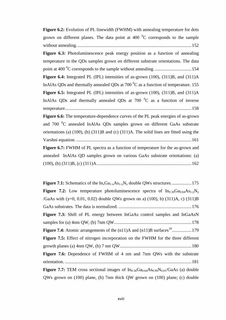
Figure 6.2: Evolution of PL linewidth (FWHM) with annealing temperature for dots
grown on different planes. The data point at 400 0C corresponds to the sample
without annealing. .................................................................................................... 152
Figure 6.3: Photoluminescence peak energy position as a function of annealing
temperature in the QDs samples grown on different substrate orientations. The data
point at 400 0C corresponds to the sample without annealing. ................................ 154
Figure 6.4: Integrated PL (IPL) intensities of as-grown (100), (311)B, and (311)A
InAlAs QDs and thermally annealed QDs at 700 0C as a function of temperature. 155
Figure 6.5: Integrated PL (IPL) intensities of as-grown (100), (311)B, and (311)A
InAlAs QDs and thermally annealed QDs at 700 0C as a function of inverse
temperature. .............................................................................................................. 158
Figure 6.6: The temperature-dependence curves of the PL peak energies of as-grown
and 700 0C annealed InAlAs QDs samples grown on different GaAs substrate
orientations (a) (100), (b) (311)B and (c) (311)A. The solid lines are fitted using the
Varshni equation. ..................................................................................................... 161
Figure 6.7: FWHM of PL spectra as a function of temperature for the as-grown and
annealed InAlAs QD samples grown on various GaAs substrate orientations: (a)
(100), (b) (311)B, (c) (311)A. .................................................................................. 162
Figure 7.1: Schematics of the InxGa1-xAs1-yNy double QWs structures. ................. 175
Figure 7.2: Low temperature photoluminescence spectra of In0.36Ga0.64As1-yNy
/GaAs with (y=0, 0.01, 0.02) double QWs grown on a) (100), b) (311)A, c) (311)B
GaAs substrates. The data is normalized. ................................................................ 176
Figure 7.3: Shift of PL energy between InGaAs control samples and InGaAsN
samples for (a) 4nm QW, (b) 7nm QW.................................................................... 178
Figure 7.4: Atomic arrangements of the (n11)A and (n11)B surfaces18
................. 179
Figure 7.5: Effect of nitrogen incorporation on the FWHM for the three different
growth planes (a) 4nm QW, (b) 7 nm QW............................................................... 180
Figure 7.6: Dependence of FWHM of 4 nm and 7nm QWs with the substrate
orientation. ............................................................................................................... 181
Figure 7.7: TEM cross sectional images of In0.36Ga0.64As0.99N0.01/GaAs (a) double
QWs grown on (100) plane, (b) 7nm thick QW grown on (100) plane; (c) double

xix
QWs grown on (311)A plane, (d) 7nm thick QW grown on (311)A plane, (e) double
QWs grown on (311) B plane, (f) 7nm thick QW grown on (311)B plane. ............ 183
Figure 7.8: EDX profiles of In composition (a) 4nm QWs grown on (100), (311)A,
(311)B planes, (b) 7nm QW grown on (100), (311)A, (311)B planes. .................... 184
Figure 7.9: HAADF of 7nm In0.36Ga0.64As0.99N0.01/GaAs QW grown on (a) (100)
plane, (b) (311)A plane, (c) (311)B plane. .............................................................. 185
Figure 7.10: Temperature dependent PL of GaInAs1-yNy/GaAs DQWs grown on
(100) GaAs plane: (a) y=0, (b) y=0.01, (c) y=0.02. ................................................. 188
Figure 7.11: Temperature dependent PL of GaInAs1-yNy/GaAs DQWs grown on
(311)A GaAs plane: (a) y=0, (b) y=0.01, (c) y=0.02. .............................................. 189
Figure 7.12: Temperature dependent PL of GaInAs1-yNy/GaAs DQWs grown on
(311)B GaAs plane: (a) y=0, (b) y=0.01, (c) y=0.02. .............................................. 190
Figure 7.13: Evolution of PL peak energies as a function of temperature for 4 and
7nm GaInAs QWs grown on (a) (100) plane, (b) (311)A plane, and (c) (311)B plane.
The solid red lines are fitting curves using the empirical Varshni model. ............... 192
Figure 7.14: Evolution of the temperature of the PL peak energies of the
GaInAs0.99N0.01/GaAs QWs grown on (100), (311)A, (311)B GaAs planes; (a)
QW=4nm (N=0.01); (b) QW=7nm (N =0.01). ........................................................ 197
Figure 7.15: Evolution of the temperature of the PL peak energies of the
GaInAs0.98N0.02/GaAs QWs grown on (100), (311)A, (311)B GaAs planes (a)
QW=4nm (N=0.02); (b) QW=7nm (N=0.02). ......................................................... 198
Figure 8.1: 10 K PL spectra of as-grown, and 500 0C, 600
0C and 700
0C annealed
In0.36Ga0.64As/GaAs DQWs samples: (a) (100), (b) (311)A, (c) (311)B. The times
number in front of each spectrum corresponds to the PL relative intensity, referred to
as enhancement factor F=Ipeak (annealed)/Ipeak (as-grown)....................................... 210
Figure 8.2: Dependence of PL energy-shift on RTA temperature for
In0.36Ga0.64As/GaAs QWs grown on (100), (311)A, and (311)B GaAs planes: a) 4nm
QW samples; b) 7nm QW samples. The data point at 400 0C corresponds to the
sample without annealing, i.e. as-grown. ................................................................. 211
Figure 8.3: Dependence of PL FWHM on RTA temperature for (100), (311)A, and
(311)B In0.36Ga0.64As/GaAs QWs: a) 4nm QW samples; b) 7nm QW. The data point
at 400 0C corresponds to the sample without annealing, i.e. as-grown. ................... 213

xx
Figure 8.4: 10 K PL spectra of as-grown, and 500 0C, 600
0C and 700
0C annealed
In0.36Ga0.64N0.01As0.99/GaAs DQWs samples: (a) (100), (b) (311)A, (c) (311)B. The
times number in front of each spectrum corresponds to the PL relative intensity,
referred to as enhancement factor F=Ipeak (annealed)/Ipeak (as-grown). .................... 214
Figure 8.5: Dependence of PL energy-shift on RTA temperature for (100), (311)A,
and (311)B InGaAs0.99N0.01/GaAs QWs: a) 4nm QW samples b) 7nm QW. The data
point at 400 0C corresponds to the sample without annealing, i.e. as-grown. ......... 216
Figure 8.6: ToF-SIMS depth profile of In and Ga ions in as-grown and annealed
In0.36Ga0.64N0.01As0.99/GaAs DQWs samples: (a) (100), (b) (311)A, (c) (311)B. .... 220
Figure 8.7: SIMS profile of nitrogen atoms in as-grown and annealed
In0.36Ga0.64N0.01As0.99/GaAs DQWs samples: (a) (100), (b) (311)A, (c) (311)B. .... 221

xxi
LIST OF TABLES
Table 2.1: lattice constant (a), energy gap (Eg) at 300K, type of energy gap, and
lattice structure of group IV elements. ....................................................................... 13
Table 2.2: lattice constant, energy gap, type and crystal structure of most important
III-V compound semiconductors................................................................................ 13
Table 2.3: Miller indices and their represented plane or direction of a crystal surface.
.................................................................................................................................. 23
Table 2.4: Some important properties of intrinsic GaAs, AlAs and AlGaAs at 300K;
HH and LH stand for heavy hole and light hole, respectively,. ................................. 44
Table 2.5: Fundamental processes in semiconductors. ............................................. 53
Table 5.1: PL peak energy (eV), FWHM (meV) and PL intensity ratios between
(100) QDs and high index QDs. ............................................................................... 109
Table 5.2: PL peak energy (eV), FWHM (meV), and PL intensity ratios between 13
Å (4.4 MLs)(100) QDs and high index QDs............................................................ 120
Table 5.3: Investigated samples having different Al content in the confining barrier.
................................................................................................................................ 128
Table 5.4: The PL properties of Al0.35In0.65As / AlyGa1−yAs QDs. ........................ 129
Table 5.5: Al0.35In0.65As/Al0.45Ga0.55As (311)B QDs samples grown at various
temperatures. ............................................................................................................ 133
Table 5.6: Summary of PL properties of Al0.35In0.65As/Al0.45Ga0.55As (311)B QDs
samples grown at various temperatures. .................................................................. 135
Table 6.1: Summary of photoluminescence emission parameters from (100),
(311)A, (311)B QDs. Blue shifts and reductions in FWHM refer to samples annealed
at 700 °C for 30 s. .................................................................................................... 151
Table 6.2: Arrhenius’s parameters for the temperature dependence of the total
integrated PL peak intensity for as-grown and annealed QDs grown on different
GaAs substrate orientations...................................................................................... 157

xxii
Table 7.1: Comparison of optical parameters of In0.36Ga0.64As and In0.36Ga0.64As1-yNy
(x=1 and 2%) QWs grown on (100), (311)A and (311)B GaAs substrates. ............ 177
Table 7.2: PL energy of 4 and 7 nm In0.36Ga0.64As1-yNy/GaAs QWs at 10K and
290K. ........................................................................................................................ 191
Table 7.3: Fitting parameters of Varshni empirical formula for 4 and 7nm GaInAs
double QWs grown on different substrate orientations............................................ 193
Table 7.4: Varshni’s parameters for the temperature dependence of the PL peak
energy for DQWs grown on different substrate orientations with different N
concentrations. ......................................................................................................... 196
Table 8.1: Investigated samples grown on different substrate orientations and having
different nitrogen contents. ...................................................................................... 208

1
CHAPTER 1: INTRODUCTION

2
1.1 INTRODUCTION
Modern electronic devices (e.g., integrated circuits) are dominated by silicon
material. However, there are some basic limitations of Si. These include lower
carrier mobility and the indirect nature of its energy-gap as compared for example to
GaAs. These properties limit its applications in the field of high speed/frequency
electronics and optoelectronics.
The III–V compounds particularly GaAs are alternative and important
semiconductors for various device applications. In general, these materials
crystallize with a relatively high degree of stoichiometry and can easily be doped as
n or p-type. Many of these III– V semiconductors materials (e.g., GaAs, InAs, InP,
and InSb) have direct energy gaps in addition to high carrier mobilities (a direct
indication of the speed electrons attain and the distance they travel before a
scattering event occurs). Therefore, this family of semiconductors offers a wide
range of applications in the field of optoelectronic devices for both the detection and
generation of electromagnetic radiation, and also in high-speed electronic devices.
Along with the binary III– V compounds, ternary III-V semiconductor materials (e.g.
AlxGa1-xAs and GaAs1-xInx) and quaternary (e.g. GaxIn1-xAs1-yNy) alloys with
“tunable” properties have great importance in many versatile applications.
By choosing carefully the composition (i.e., x and y), it is possible to select a
particular semiconductor property (e.g., the energy gap) to fit specific device
requirements.
In such cases, these compounds are typically grown as epitaxial layers in
heterojunction systems on substrates such as GaAs or InP, e.g., AlxGa1-xAs on GaAs,
or GaxIn1-xAsyN1-y on InP. One of the important parameters that should be taken into
account in the epitaxial growth of heterostructures is the lattice constant mismatch
between the epitaxial layer and the substrate. A larger lattice mismatch results in the
generation of dislocations in the epitaxial layer.
GaAs is often used as substrate material for the epitaxial growth of many III-V
semiconductors including InAlAs and GaInNAs. The properties of such substrates
have a major effect on the subsequent growth and properties of the epitaxial layers.
The conventional plane direction of GaAs substrate is (100) but other non-
conventional plane directions have been used previously. For example, the structural,

3
optical and electrical properties of III-V based structures are found to change and/or
improve by growing on non-conventional (n11) planes. In addition, the study of
molecular beam epitaxy (MBE) growth on substrates with different orientations has
provided useful information on the epitaxial growth mechanism.
Semiconductors structures grown on high index substrates have fascinating
properties which are not found in similar structures grown on (100) oriented
substrates such as optical anisotropy1,2
, high hole mobility3,4
and better optical
efficiency5-11
.
In this thesis two emerging and technologically important III-V semiconductors,
namely InAlAs Quantum dots and dilute nitrides InGaAsN Quantum wells grown on
conventional and non-conventional GaAs substrates, have been studied using
structural and optical techniques. A brief summary of the importance of these two
materials systems is given in the following sections.
1.2 InAlAs QUANTUM DOTS
Nanotechnology is considered to be one of the corner stone of the next technological
revolution after the industrial revolution of the middle of the eighteenth century.
Quantum Dots (QDs) and Quantum Wells (QWs) are nanoscale structures created by
confining free electrons (or holes) in a three-dimensional (3D) and two-dimensional
(2D) semiconducting matrix, respectively. These nanostructures of confined
electrons present many interesting electronic and optoelectronic properties. They are
of potential importance for applications in quantum computing, biological labeling,
and lasers, to name only a few.
During the last years, considerable interest has been devoted to the fabrication of
self-assembled quantum dots (QDs). Stranski-Krastanow (SK) MBE technique has
been used to grow these QD nanostructures where 3D confinement regions were
obtained. This process leads to a strained epitaxial layer. The deposited material
often grows in a layer-by-layer mode until a certain critical thickness, beyond which
3D islands form through what is known as the SK transition.
Compared to the InxGa(1-x)As/GaAs QDs that emit in the infrared region, relatively
few investigations on InAlAs/AlGaAs QDs emitting in the visible region have been
4
reported in the literature. InAlAs QDs have the advantage of having a luminescence
in the red part of the electromagnetic spectrum. This visible wavelength in particular
is advantageous for ophthalmology treatment12
. In addition, it is important for many
other different applications ranging from high-density optical storage to
photodynamic therapy13,14
. However, there are some difficulties in fabricating high
optical quality InAlAs/AlGaAs QDs. These are due to the incorporation of impurities
such as oxygen and formation of group-III vacancies during the growth process15,16
.
The use of high index planes could improve the optical and structural properties of
InAlAs/AlGaAs QDs as demonstrated in many other QDs systems.
1.3 DILUTE NITRIDE III-V ALLOYS (InGaAsN)
Lasers emitting in the wavelengths 1.3 μm and 1.55 μm have generated great interest
for applications in optical fiber communications. The 1.3 μm wavelength is attractive
due to zero dispersion in the silica based optical fiber, and 1.55 μm, has the lowest
optical loss. For these reasons, it is important to have a light emitter which works at
wavelengths of 1.3 and 1.55 μm.
Currently, telecommunication edge-emitting lasers operating in 1.3 µm and 1.55µm
range are based on the conventional GaInAsP alloys grown on InP substrates.
However, InP substrates are very expensive compared to GaAs substrates. Therefore,
an attractive approach to reduce cost is to fabricate telecommunication lasers on
GaAs substrates.
The introduction of N into GaAs leads to giant bowing of bandgap energy, unlike the
conventional III-V alloys (shown in Figure 1.1). Incorporation of 1% nitrogen leads
to a band gap reduction of GaAs by 125 meV17
. The lowering of the bandgap energy
of GaAs extends the emission wavelength of GaAs-based devices to 1.3 μm (and
beyond) and makes it suitable for fabricating infrared lasers which would be
alternative to GaInAsP/InP lasers.
Nitrogen incorporation in GaAs lattice introduces a tensile strain. While
incorporation of In leads to a compressive strain. Therefore, a lattice matching with
GaAs can be achieved by strain compensation between nitrogen and indium.

5
GaInNAs alloy will be lattice matched to GaAs provided that the In:N ratio is ~
3:118
.
Figure 1.1: Band gap versus lattice constant for various III-V alloys19
.
GaInAsN alloys grown on GaAs have several additional advantages vis-a-vis
InGaAsP/InP. GaAs based material systems (InGaAsN/GaAs) offer high conduction
band (CB) offset, which provides stronger carrier confinement over GaInAsP /InP
leading to devices which have properties that are temperature-insensitive and operate
at higher maximum temperatures20,21
. For example, Tansu et al22
demonstrated an
InGaAsN/GaAs laser with a room-temperature emission wavelength and threshold
current density of 1.3 µm and 210-270 A/cm2, respectively.
Another advantage of GaInNAs is that it can easily be integrated with highly
reflective GaAs/AlAs Brag mirrors which are used for the fabrication of vertical
cavity surface emitting lasers (VCSELs). Integration techniques of GaAs/AlAs Brag
mirrors are already mature.
5.4 5.5 5.6 5.7 5.8 5.9 6 6.1 6.2
AlAs
InxAl1-xAs AlxGa1-xAs
InxGa1-xAs
InP GaAs
GaNyAs1-y
GaxIn1-xNyAs1-y
InxGa1-xAsyP1-y
InAs
InNyAs1-y
1.30µm
1.55µm
0
0.5
1
1.5
2
2.5
Ban
dga
p (
eV
)
Lattice Parameter (Å)

6
The first GaAsN alloy was grown by metalorganic chemical vapor deposition23
, and
a strong bandgap reduction of the alloys was observed. Shortly after GaAsN was
successfully grown using gas source MBE with a N composition of 4%24
.
In order to achieve such longer emission wavelengths, nitrogen incorporation is a
major issue that has to be further addressed. Growth mechanisms depend strongly on
the surface atomic arrangement and the substrate orientation. Taking into account
these two parameters in the growth of dilute III-V nitrides could yield an
enhancement of nitrogen incorporation and optical efficiency. However, it was
observed that both the optical and crystal quality of N-diluted alloys are partially
degraded when the N concentration is increased25
. In addition, the use of high index
GaAs planes could also improve the optical quality of III- V dilute nitrides alloys.
In this thesis, the results of a comprehensive study of the optical properties of
InAlAs QDs and InGaAsN QWs grown by MBE on both the conventional (100) and
high Miller index surfaces are presented.
1.4 ORGANIZATION OF THE THESIS
This thesis is organized as follows:
Chapter 1 contains the research motivations and outlay of the thesis.
Chapter 2 is devoted to the description of the fundamental concepts of
semiconductors, including their crystal structure and optical processes. The
principles of III-V compound heterostructures and dilute III-V nitride alloys are
presented. The importance and growth of III-V compound materials on high index
planes will be also covered
Chapter 3 provides information on fundamental concepts and molecular beam
epitaxial growth of low dimensional semiconductor structures.
Chapter 4 explains the experimental techniques used in this thesis including
Photoluminescence (PL), Transmission electron microscopy (TEM), and Secondary

7
ion mass spectroscopy (SIMS). The description of their hardware and soft software
implementation will be presented.
Chapter 5 is based on the PL experimental results for a set of InAlAs QDs grown at
different growth conditions (growth temperature, amount of material, different
capping composition) on (100), (311)A and (311)B GaAs substrates.
Chapter 6 reports the effect of annealing on the as-grown InAlAs QDs grown on
(100), (311)A and (311)B GaAs substrates
Chapter 7 presents the effect of nitrogen incorporation on the optical and structural
properties of GaInNAs/GaAs double quantum well (DQWs) grown on different
GaAs substrate orientations, namely (100), (311)A, and (311)B.
Chapter 8 describes the effect of annealing on the as-grown GaInAs1-xNx (x=0, and
1%) double QWs grown on (100), (311)A and (311)B GaAs substrates.
Chapter 9 is based on the overall conclusion of the research work carried out in this
thesis and suggestions for future work.

8
REFERENCES
1 E. C. Valadares, Physical Review B, 46 (1992) 3935.
2 R. Notzel, N. N. Ledentsov, L. Daweritz, K. Ploog, M. Hohenstein, Physical
Review B, 45 (1992) 3507.
3 W. I. Wang, E. E. Mendez, Y. Iye, B. Lee, M. H. Kim, and G. E. Stillman, Journal
of Applied physics, 60, 1834, (1986).
4 A. Davies, J. Frost, D. Ritchie, D. Peacock, R. Newbury, E. Linfield, M. Pepper,
and G. Jones, Journal of Crystal Growth, 111, 318 (1991).
5 D. I. Lubyshev, P. P. Gonzalez-Borrero, E. Marega, E. Petitprez, and P. Basmaji,
The Journal of Vacuum Science and Technology B, 14 (3), 2212 (1996).
6 P. O. Vaccaro, M. Hirai, K. Fujita, and T. Watanabe, Journal of Physics D: Applied
Physics, 29 (9), 2221(1996).
7 R. Notzel, Semiconductor Science and Technology, 11 (10), 1365 (1996).
8 K. Nishi, T. Anan, A. Gomyo, S. Kohmoto, and S. Sugou, Applied Physics Letters,
70 (26) 3579, (1997).
9 M. Kawabe, Y. J. Chen, S. Nakajima, and K. Akahare, Japanese Journal of Applied
Physics, 36 (6B) 4078 (1997).
10 K. Nishi, R. Mirin, D. Leonard, G. Medeiros-Ribeiro, P. M. Petroff, and A.
Gossard, Journal of Applied Physics, 80 (6), 3466 (1996).
11 M. Henini, A. Polimeni, A. Patane, L. Eavesa, P.C. Maina, and G. Hill,
Microelectronics Journal, 30, 319 (1999).
12
D. J. Browning, and C. M. Fraser. Ophthalmology , 112, 1054 (2005).
9
13
R. Singh, D. Bull, F. P. Dabkowski, E. Clausen, and A. K. Chin, Applied Physics
Letters, 75, 2002 (1999).
14 K. Hinzer, J. Lapointe, Y. Feng, A. Delage, S. Fafard, A. J. SpringThorpe, and E.
M. Griswold, Journal of Applied Physics, 87, 1496 (2000).
15 W. I. Wang, S. Judaprawira, C. E. C. Wood, and L. F. Eastman, Applied Physics
Letters, 38, 708 (1981).
16 Y. Horikoshi, M. Kawashima, and H. Yamaguchi, Applied Physics Letters, 50,
1686 (1987).
17 S. Tixier, M. Adamcyk, T. Tiedje, S. Francoeur, A. Mascarenhas, P. Wei, and F.
Schiettekatte, Applied Physics Letters, 82, 2245, (2003).
18 L. Bellaiche, Applied Physics Letters, 75, 2578, (1999).
19 Dilute Nitride Semiconductors, Edited by M. Henini, Elsevier Science (2005).
20 M. Kondow, S. Nakatsuka, T. Kikatani, Y. Yazawa, and M. Okai, Japanese
Journal of Applied Physics, 35(11), 5711 (1996).
21 M. Kondow, K. Uomi, A. Niwa, T. Kitatani, S. Watahiki, and Y. Yazawa,
Japanese Journal of Applied Physics, 33, 1273 (1996).
22 N. Tansu, JY. Yeh, and L. Mawst, Applied Physics letter, 83, 2512, (2003).
23 M. Weyers, and M. Sato. Japanese Journal of Applied Physics, 853, 31, (1992).
24 M. Kondow, K. Uomi, K. Hosomi, and T. Mozume, Japanese Journal of Applied
Physics, L1056, 33, (1994).

10
25
H. P. Xin, K. L. Kavanagh, and C. W. Tu, Journal of Crystal Growth, 208, 145
(2000).

11
CHAPTER 2: FUNDAMENTAL CONCEPTS OF
SEMICONDUCTORS

12
In this chapter the fundamental concepts of semiconductors will be presented
including their crystal structure and optical processes. The emphasis will be on
heterostructures and meaning of high index plane since these form a key aspect to
understanding the optical properties of quantum dots and quantum wells investigated
in this work.
2.1 INTRODUCTION
In the last thirty years substantial advances have been realised in the research and
applications of semiconductors. It is well known that semiconductor technology has
a great impact on our society. For example it is well-known that personal computers,
which are in almost everyone’s house and office, have changed the way we
communicate. Semiconductor applications are present everywhere around us: on
roads, in houses, in schools, and even in our pockets. Semiconductor research is still
attracting increased interest at all scientific levels because of their multitude of
applications.
Solid materials are generally classified according to the value of the energy gap
between their conduction and valence bands. Most of the common materials have
energy gaps in the range from zero to few electron volts (eV). According to this
classification materials having an energy gap of ~ 0 eV are referred to as metals or
semi-metals. On the other hand, materials with energy gaps larger than 3 eV are
frequently known as insulators, whereas semiconductor materials have energy gaps
bridging from ~0.1 eV to ~ 3 eV.
Semiconductors behave as insulators at absolute zero temperature (T = 0K) but their
electrical conductivity increases rapidly with increasing temperature. Furthermore,
the electrical conductivity can be controlled by adding small amounts of certain
impurities, so-called dopants, or by illumination with particular wavelengths of light.
These properties contrast strongly with those of good conductors such as metals,
which contain large densities of free electrons that originate from the valence
electrons of the metal atoms. The electrical conductivity of metals, which is many
orders of magnitude larger than that of semiconductors, decreases relatively weakly

13
with increasing temperature and, to a good approximation, is not affected by small
levels of impurities or illumination.
Semiconductor materials are classified according to their chemical composition.
There are elementary semiconductors such as Si and Ge which are elements of group
IV of the periodic table of elements. Some of the elemental semiconductors and their
properties are listed in Table 2.1.
Table 2.1: lattice constant (a), energy gap (Eg) at 300K, type of energy gap, and
lattice structure of group IV elements.
Material a (nm) Eg (eV) Type Structure
Diamond ( C ) 0.357 5.48 Indirect Cubic
Silicon (Si) 0.543 1.12 Indirect Cubic
Germanium (Ge) 0.566 0.664 Indirect Cubic
Compound semiconductor materials are formed from two or more elements from the
different groups of the periodic table. For example GaAs is the best known III-V
compound material, which is formed by combining Gallium (Ga), group III element,
with Arsenic (As), group V element. Other III-V compound semiconductors include
InP and GaP. One can combine GaAs and AlAs to obtain ternary III-V compound
AlxGa1-xAs, where x and (1-x) represent the content of Al and Ga in the alloy,
respectively. Another important class of semiconductors is known as II-VI
compound materials such as Zinc Sulphide (ZnS) and Mercury Cadmium Telluride
(HgCdTe). Most important III-V compounds are presented in Table 2.2 together with
their respective properties.
Table 2.2: lattice constant, energy gap, type and crystal structure of most important
III-V compound semiconductors1.
Material a (nm) Eg (eV) Type Structure
GaAs 0.565 1.424 Direct Cubic
InAs 0.606 0.354 Direct Cubic
AlAs 0.566 2.15 Indirect Cubic
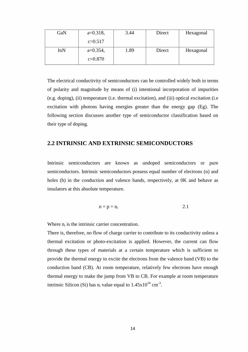
14
GaN a=0.318,
c=0.517
3.44 Direct Hexagonal
InN a=0.354,
c=0.870
1.89 Direct Hexagonal
The electrical conductivity of semiconductors can be controlled widely both in terms
of polarity and magnitude by means of (i) intentional incorporation of impurities
(e.g. doping), (ii) temperature (i.e. thermal excitation), and (iii) optical excitation (i.e
excitation with photons having energies greater than the energy gap (Eg). The
following section discusses another type of semiconductor classification based on
their type of doping.
2.2 INTRINSIC AND EXTRINSIC SEMICONDUCTORS
Intrinsic semiconductors are known as undoped semiconductors or pure
semiconductors. Intrinsic semiconductors possess equal number of electrons (n) and
holes (h) in the conduction and valence bands, respectively, at 0K and behave as
insulators at this absolute temperature.
n = p = ni 2.1
Where ni is the intrinsic carrier concentration.
There is, therefore, no flow of charge carrier to contribute to its conductivity unless a
thermal excitation or photo-excitation is applied. However, the current can flow
through these types of materials at a certain temperature which is sufficient to
provide the thermal energy to excite the electrons from the valence band (VB) to the
conduction band (CB). At room temperature, relatively few electrons have enough
thermal energy to make the jump from VB to CB. For example at room temperature
intrinsic Silicon (Si) has ni value equal to 1.45x10¹⁰
cm-3
.

15
Extrinsic semiconductors are obtained by introducing different atoms, called dopant
atoms, into the host crystal. Two types of extrinsic materials can be fabricated as
shown in Figure 2.1 for the case of silicon semiconductor:
(1) n-type material: the dopant atoms added to the semiconductor crystal are called
donor atoms.
For silicon, phosphorus (P), arsenic (As) or antimony (Sb) can be used as donors.
These donors that belong to column V in the periodic table have five electrons in
their outermost shell. When these atoms are incorporated in the silicon crystal, one
of the electrons in this shell can easily jump to the conduction band, leaving a
positively charged atom behind. This process is sometimes called “activation” or
“ionization” of the donor atoms. This energy is very small compared to the silicon
band gap so it can easily be ionized at room temperature. The positively charged
donor atoms that are left behind after ionization is immobile and does not contribute
to electrical conduction. The electron leaving the atom is free and contribute to the
electron concentration (n). Because the activation energy is low, almost all of the
donor atoms intentionally incorporated in the crystal will give an electron to the
conduction band at room temperature. So if ND is the donor concentration with one
additional valence electron, for an n-type material at T ≠ 0K, excess electrons from
dopant atoms may be excited thermally from their states within the forbidden band
gap which is located slightly below the bottom of the conduction band, increasing
the free electron density (n0).
n0 ≈ ND (cm-3) 2.2
(2) p-type material: the dopant atoms in this case are named acceptor atoms. In
silicon, Boron (B), Aluminium (Al) and Gallium (Ga) are employed as acceptors.
These atoms which belong to column III have three electrons in their outermost
shell. When these atoms are added in the silicon crystal, one of the electrons in the
silicon valence band can easily jump to the valence shell of one of the acceptor
atoms, leaving a hole behind and making the acceptor atom negatively charged. The
negatively charged acceptor atom is immobile and does not contribute to the
electrical conduction. The hole left behind contributes to the hole concentration (p).
Because the activation energy at room temperature is low almost all of the
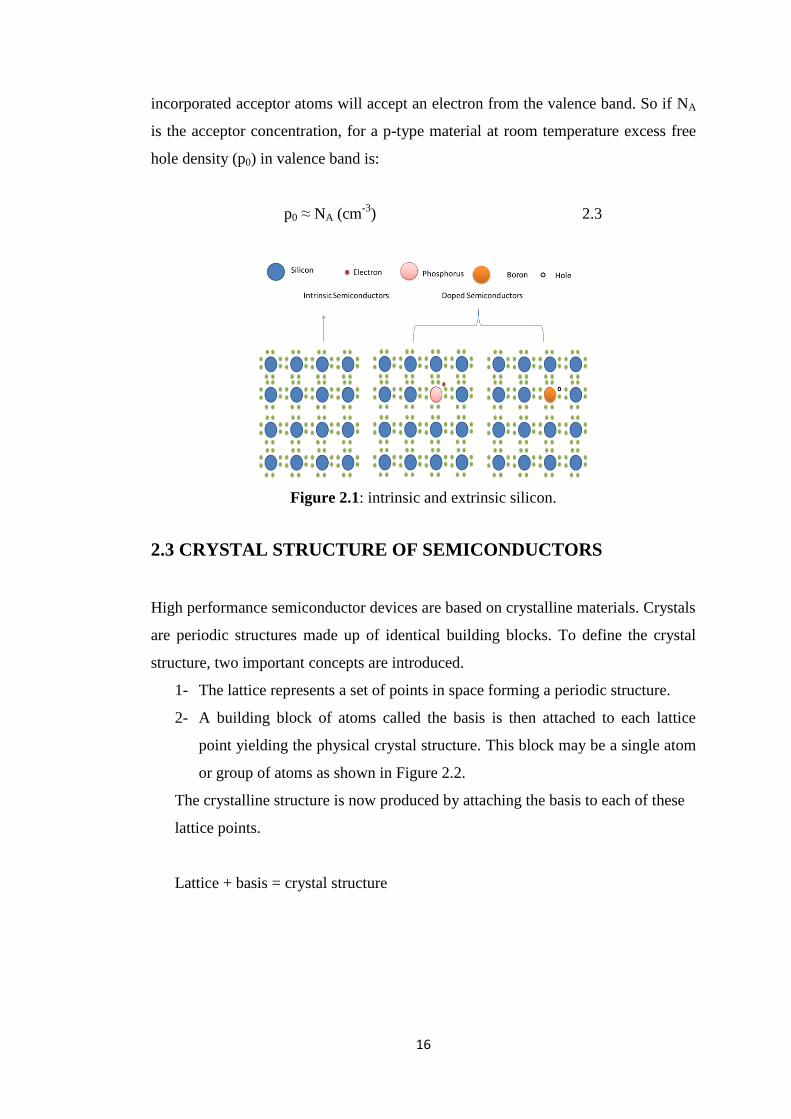
16
incorporated acceptor atoms will accept an electron from the valence band. So if NA
is the acceptor concentration, for a p-type material at room temperature excess free
hole density (p0) in valence band is:
p0 ≈ NA (cm-3
) 2.3
Figure 2.1: intrinsic and extrinsic silicon.
2.3 CRYSTAL STRUCTURE OF SEMICONDUCTORS
High performance semiconductor devices are based on crystalline materials. Crystals
are periodic structures made up of identical building blocks. To define the crystal
structure, two important concepts are introduced.
1- The lattice represents a set of points in space forming a periodic structure.
2- A building block of atoms called the basis is then attached to each lattice
point yielding the physical crystal structure. This block may be a single atom
or group of atoms as shown in Figure 2.2.
The crystalline structure is now produced by attaching the basis to each of these
lattice points.
Lattice + basis = crystal structure

17
Figure 2.2: The formation of the crystal structure from the combination of lattice
and basis is shown. The basis may consist of one atom (A) or group of atoms (B).
To define a lattice one need to define three primitive translation vectors a1, a2, and
a3, such that any lattice point C can be obtained from any other lattice point R by a
translation
C = R + c1a1 + c2a2 + c3a3 2.4
Where c1, c2, c3 are integers.
The translation vectors a1, a2, and a3 are called primitive if the volume of the cell
formed by them is the smallest possible. The volume cell enclosed by the primitive
vectors is called the primitive unit cell. There is no unique way to choose the
primitive vectors. It is possible to define more than one set of primitive vectors for a
given lattice, and often the choice depends upon convenience.
2.3.1 Basic Lattice Types
There are 14 types of lattices. These lattice classes are defined by the relationships
between the primitive vectors a1, a2, and a3, and the angles α, β, and γ between them.
The most important types of primitive cells, known as cubic and hexagonal lattices,
underlay the structure taken by all semiconductors.
There are 3 kinds of cubic lattices: simple cubic, body centred cubic (bbc), and face
centred cubic (fcc).

18
The simple cubic lattice shown in Figure 2.3 is generated by the primitive vectors ax,
ay, az where x, y, z are unit vectors.
Figure 2.3: A simple cubic lattice showing the primitive vectors. The crystal is
produced by repeating the cubic cell through space.
The bcc lattice, shown in Figure 2.4 can be generated from the simple cubic structure
by placing a lattice point at the centre of the cube. If x , y , and z are three
orthogonal unit vectors, then a set of primitive vectors for the bbc lattice is given by
a1 = a x , a2 = a y , 3 ˆ ˆ ˆ( )2
aa x y z 2.5
Figure 2.4: The body centred cubic lattice along with a choice of primitive vectors.

19
The fcc lattice, shown in Figure 2.5, can be obtained by extending the cubic lattice
by adding an atom to the center of each face of the cube (leading to a lattice with 14
atoms). The lattice constant a is the side dimension of this cube.
A symmetric set of primitive vectors for the fcc lattice are given by:
1 2 3ˆ ˆ ˆ ˆˆ ˆ( ), ( ), ( )2 2 2
a a aa y z a z x a x y 2.6
Figure 2.5: Primitive basis vectors for the face centered cubic lattice.
The semiconductors studied in this work have an underlying fcc lattice. The full
lattice structure as illustrated in Figure 2.6 combines two of these fcc lattices, one
lattice interpenetrating the other (i.e., the corner of one cube is positioned within the
interior of the other cube, with the faces remaining parallel). The coordinates of the
two basis atoms are 000 and , ,4 4 4
a a a
. For the III-V and II-VI semiconductors
with this fcc lattice foundation, one fcc lattice is constructed from one type of
element (e.g., atom from group III) and the second fcc lattice is constructed from the
other type of element (e.g., atom from group V). In the case of ternary and
quaternary semiconductors, elements from the same atomic group are placed on the
same fcc lattice. All bonds between atoms occur between atoms in different fcc

20
lattices. For example, all Ga atoms in the GaAs crystal are located on one of the fcc
lattices and are bonded to As atoms, all of which appear on the second fcc lattice.
The interatomic distances between neighbouring atoms are therefore less than the
lattice constant. If the two fcc lattices contain elements from different groups of the
periodic chart, the overall crystal structure is called the zinc blende lattice. Most
popular elemental semiconductor materials such as silicon, germanium, and carbon
have the diamond like structure, which is formed between the same types of atoms.
In diamond structure each atom makes bonds with four adjacent atoms of the same
group. The bonds between silicon atoms in the silicon crystal extend between fcc
sublattices.
Although the common semiconductor materials share this basic diamond/zinc blende
lattice structure, some semiconductor crystals are based on a hexagonal close-packed
(hcp) lattice. Typical examples are CdS and CdSe from the II-VI semiconductor
family. In this example, all the Cd atoms are located on one hcp lattice while the
other atom (S or Se) is located on a second hcp lattice. Similarly to the diamond and
zinc blende lattices described above, the complete lattice is constructed by
interpenetrating these two hcp lattices. The overall crystal structure is called a
wurtzite lattice.
IV-VI semiconductors (PbS, PbSe, PbTe, and SnTe) exhibit a narrow band gap and
have been used for infrared detectors. Their lattice structure is the simple cubic
lattice, also the so-called NaCl lattice.
Figure 2.6: The zinc blende crystal structure consists of the interpenetrating fcc
lattices, one displaced from the other by a distance , ,4 4 4
a a a
along the body
diagonal. The underlying Bravais lattice is fcc with a two atoms basis. The positions
of the two atoms is (000) and , , .4 4 4
a a a

21
2.3.2 The Reciprocal Lattice and Miller Indices
Miller indices are used to label crystal planes with the familiar (hkl) notation based
on their intercepts with the crystallographic reference axes. As for directions,
negative indices are often indicated by a bar or minus sign written above the
corresponding index, e.g. (00 1 ). Every crystal has two lattices associated with it, a
crystal lattice and a reciprocal lattice. A diffraction pattern of a crystal is a map of
the reciprocal lattice of the crystal.
The reciprocal basis vectors can be derived as follow:
The crystalline solid can be described by a, b, and c, which are the primitive basis
vectors in such a way that the crystal structure remains the same under translation
through a vector. The translation vector is an integral multiple of the basis vectors (a,
b, and c) and is defined as
R ma nb rc 2.7
here m, n, and r are integers and a, b ,and c are the primitive vectors
This definition then leads to expressions for the reciprocal basis vectors:
a* = (b x c) /a . (b x c) 2.8
b* = (c x a ) / a . (b x c) 2.9
c* = (a x b) / a . (b x c) 2.10

22
The reciprocal lattice vector g, with components (h,k,l) is perpendicular to the plane
with Miller indices (hkl), so often denoted as ghkl:
ghkl = ha* + kb* + lc* 2.11
And
|ghkl | = 1/dhkl 2.12
Where dhkl is the spacing between lattice planes
Figure 2.7 shows some planes of a cubic lattice with their Miller indices. Similarly to
directions, some of the planes are also equivalent for symmetry reasons, e.g. planes
(110), ( 1 10), (0 1 1) etc. in a cubic crystal. Such equivalent planes are collectively
denoted as {110}. The method of finding the Miller indices is discussed below.
Consider a three dimensional crystal plane whose three basis vectors are x, y, and z.
The Miller indices of this plane can be obtained in the following way:
(i) Find the intercepts of the planes along three basis vectors (these
intercepts can be in terms of lattice constant or primitive cells).
(ii) Take the reciprocals of intercepts along each axis.
(iii) Reduce the reciprocals of these intercepts into smallest values in such a
way that the smallest three integers have the same ratio.
The result obtained from above three steps is enclosed in a parenthesis (hkl) called
the Miller indices of a single plane with intercepts at 1/h, 1/k, and 1/l on the x, y, and
z-axis, respectively. However, {hkl} represents the Miller indices of a full set of
planes of equivalent symmetry.

23
Figure 2.7: Miller indices of some important planes in a cubic crystal.
Table 2.3: Miller indices and their represented plane or direction of a crystal
surface2.
Miller
Indices
Description of plane or direction
( h k l )
For a plane that intercepts l/h, l/k, 1/l on the x-, y-, and z-axis,
respectively.
( h k l )
For a plane that intercepts the negative x-axis.
{ h k l }
For a full set of planes of equivalent symmetry, such as {100} for
(100), (0l0),
(00 l) , ( 1 00) , ( 0 1 0 ) , and(00 1 ) in cubic symmetry.
[ h k l]
For a direction of a crystal such as [100] for the x-axis.
hkl For a full set of equivalent directions.

24
The (100), (110) and (111) planes are the so-called low index planes of a cubic
crystal system (the "low" refers to the Miller indices being small numbers; 0 or 1 in
this case). Whereas, values greater than these are called high index planes such as
(210).
2.3.3 Conventional and Non-Conventional Plane
The interest in the growth of III-V compound semiconductors such as GaAs and
AlGaAs on high index planes has increased tremendously over the last decade. The
structural, optical and electrical properties of III-V based structures are found to
improve by growing on (n11) planes. The study of the molecular beam epitaxy
(MBE) growth on substrates with different orientations could provide useful
information on the epitaxial growth mechanism as well and on the physics of dopant
incorporation. The use of high Miller index substrate orientations permits the
engineering of quantum dots properties such as shape, size distribution, and
transition energy and emission polarisation, thus opening a wide range of device
design opportunities. The growth of epitaxial layers on high-index planes represents
a step forward in semiconductor material engineering, as it offers an additional
degree of freedom to develop applications with improved properties with respect to
the conventional (100) grown devices. The interest in non-(100) semiconductor
structures is manifold and concerns growth, impurity incorporation, electronic
properties, lasing performance, and piezoelectric effects. To mention a few
examples, the use of non (001) substrates has allowed the fabrication of ultrahigh
mobility two-dimensional hole gases in GaAs/AlGaAs heterostructures, high-
performance InAs/GaAs quantum dot (QD) lasers, InGaAs/GaAs QDs with
enhanced piezoelectric effects, and GaMnAs epilayers with modified Mn
incorporation and magnetic anisotropies3-6
.
The possibility of changing and improving the fundamental material properties,
growth mechanisms, surface kinetics and impurity incorporation by growing on
crystal orientations other than (100) has motivated a strong effort to study these
aspects. Some very interesting features have emerged concerning the piezoelectric

25
effect, the dopant incorporation, the self-organization of microstructures, the
ordering of ternary alloys and the over layer strain7.
Many high index polarized surfaces, such as GaAs (311)A8 and (311)B
9-13, GaAs
(411)A14
and (411) B15
, have drawn greater attention because QDs grown on theses
surfaces have some unique properties, such as the narrow size distribution and high
QDs density. These structure properties can further improve the performance of
devices. It is worth mentioning here that for the GaAs high index planes, A and B
refer to Ga and As surface, respectively.
Tilted substrates, in which the surface is other than (100), allow device researchers to
make use of extra parameters in the search for better technological structures due to
the fact that the natural roughness on high index substrates influences the dot
formation and the electronic properties of the dots, such that the photoluminescence
(PL) energy, the PL intensity, or the PL line width can change according to the
substrate orientation. Figure 2.8 illustrates such (100) plane and non-(100) planes,
also called tilted or high index planes.
Figure 2.8: illustration of (100) plane and non-100 planes (tilted or high index
planes). The black and white circles represent group V and group III atoms,
respectively.

26
The surface structure of the (211) and (311) planes are very similar, with
components of both (100) and (111) bonding geometries. The microscopic surface
structure of (211)A can be considered to be composed of periodic steps with one
(100) step edge atom and two (111) terrace atoms, while the (311) surface is
composed of equal numbers of (100) step edge and (111) terrace atoms. The (311)B
surface has a sequence of pairs consisting of an As surface atom with two dangling
bonds, as for the (100) configuration, and a Ga surface atom with one dangling bond,
as for the (111)A configuration that is identical to that of the (311)A surface with the
Ga and As atoms interchanged.
Depending on the polarity of the (111) component, the three-bond site can be group
III atom (Ga) site for (311)A orientation or group V atom (As) site for (311)B
orientation.
Each (111)B surface atom has one single-dangling bond and each (100) surface atom
has one double-dangling bond. In contrast to this, the (211)B, (311)B, and (511)B
surfaces are composed of both single-dangling bond sites and double-dangling bond
sites, making the surfaces partially (111)-like and partially (100)-like. In the case of
the (211)B surface (Figure 2.9), there are twice as many single-dangling bond sites
as there are double-dangling bond sites. Thus, the (111)-like character outweighs the
(100)-like character.
Figure 2.9: (211)B GaAs viewed along the (011) direction. The heavy line
highlights the (100) terrace structure16
.
The (311)B surface (Figure 2.10) consists of equal densities of single- and double-
dangling bond sites resulting in equal weighting of the (111)-like and (l00)-like

27
components. For the (51l)B (Figure 2.11) orientation and higher index planes, the
(l00)-like double dangling bonds outnumber the (111)-like single-dangling bonds
and thus the (l00)-like character will dominate.
Figure 2.10: (311)B GaAs viewed along the (011) direction. The heavy line
highlights the (100) terrace structure16
.
Figure 2.11: (511)B GaAs viewed along the (011) direction. The heavy line
highlights the (100) terrace structure16
Compared with an atomically flat (100) surface, a (311) plane has corrugations due
to the presence of edge steps17,18
. This could give rise to the formation of dots having
microscopic and electronic properties quite different from the ones formed on (100).
The differences between (311)B and (311)A substrates can be explained by taking
into account the surface polarity.

28
The major difference between differently misoriented substrates is in the surface step
density. The surface corresponding to the maximum step density is the (311)
orientation.
2.4 ENERGY BAND GAP
The band structure of crystalline solids, that is Energy –Momentum (E- k) relation, is
obtained by solving the Schrodinger equation of one-electron problem. For any
semiconductor there is a forbidden energy region in which allowed energy states
cannot exist. Energy regions or energy bands are permitted above and below this
energy gap. The upper bands and lower bands are called the conduction bands and
valence bands, respectively. The separation between the energy of the lowest
conduction band (Ec) and that of the highest valence band (Ev) is called the band gap
Eg which is the most important parameter of semiconductors
The shape of the conduction band and valence band near k = 0 is approximately
parabolic and their energy is given by:-
2 2
C g 2 *E E
8 e
h k
m 2.13
2 2
V g 2 *E E
8 h
h k
m 2.14
Where h is the Plank’s constant,*
em and *
hm are the effective mass of electron and
hole, respectively.
The energy-momentum relationship is described by:-

29
2
*2
pE
m 2.15
The effective mass can be obtained from the second derivative of E with respect to p
12
*
2e
d Em
dp
2.16
Similar expression can be obtained for holes (with subscript h instead of e). The
electrons and holes are treated as free particles by assigning them a modified mass,
the effective mass, which combines their potential and kinetic energies into a single
kinetic-like energy. As an example, the semiconductor GaAs has an electron
effective mass*
00.067em m and a hole effective mass *
00.35hm m where m0 is
the free electron mass.
At zero Kelvin, all the electrons are confined to the valence band and the material
behaves as an insulator. Above zero Kelvin, some electrons can have sufficient
energy to make a transition to the conduction band and contribute to the electrical
conduction process
Figure 2.12 shows a simplified energy–band structure of semiconductors. The
electron energy is conventionally defined to be positive when measured upward and
the hole energy is positive when measured downwards.
Figure 2.12: simplified energy–band structures of semiconductors.

30
2.5 DIRECT AND INDIRECT BAND GAP SEMICONDUCTOR
Bulk semiconductors are characterized by the structure of their conduction and
valence bands as being direct or indirect. The optical properties of direct gap
semiconductors differ considerably from those of indirect gap semiconductors.
Direct semiconductor (e.g. GaAs, CdS) are characterized by having the minimum
transition energy to promote an electron from the valence band to the conduction
band without a change in the electron momentum (the energy is known as the band-
gap). For indirect semiconductors, however, excitation at the band gap energy must
be accompanied by a change in the electron’s momentum (supplied by a phonon).
In indirect semiconductors, the only possible scenario for interband optical
transitions is that a phonon causes a vertical virtual transition at k= 0 with subsequent
electron-phonon scattering processes, i.e., optical transitions are allowed only if
phonons are absorbed or emitted to conserve the crystal momentum19
, as shown
schematically in Figure 2.13. In the optical absorption process a phonon is emitted or
absorbed to conserve the crystal momentum.
E electron = E photon ± E phonon 2.17
and
k electron = ± k phonon 2.18
In optical emission, a similar process takes place.
E photon= E electron ± E phonon 2.19
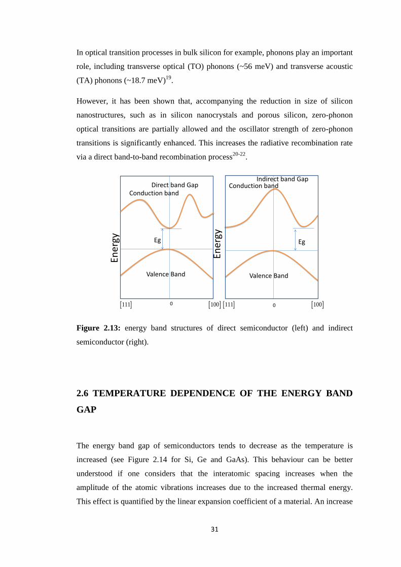
31
In optical transition processes in bulk silicon for example, phonons play an important
role, including transverse optical (TO) phonons (~56 meV) and transverse acoustic
(TA) phonons (~18.7 meV)19
.
However, it has been shown that, accompanying the reduction in size of silicon
nanostructures, such as in silicon nanocrystals and porous silicon, zero-phonon
optical transitions are partially allowed and the oscillator strength of zero-phonon
transitions is significantly enhanced. This increases the radiative recombination rate
via a direct band-to-band recombination process20-22
.
Figure 2.13: energy band structures of direct semiconductor (left) and indirect
semiconductor (right).
2.6 TEMPERATURE DEPENDENCE OF THE ENERGY BAND
GAP
The energy band gap of semiconductors tends to decrease as the temperature is
increased (see Figure 2.14 for Si, Ge and GaAs). This behaviour can be better
understood if one considers that the interatomic spacing increases when the
amplitude of the atomic vibrations increases due to the increased thermal energy.
This effect is quantified by the linear expansion coefficient of a material. An increase
100
Eg
Conduction band Direct band Gap
Valence Band
0 100 111
Ener
gy
Eg
Conduction band Indirect band Gap
Valence Band
0 111
Ener
gy

32
of the interatomic spacing decreases the potential seen by the electrons in the
material, which in turn reduces the size of the energy band gap. A direct modulation
of the interatomic distance, by applying for example high compressive (tensile)
stress, also causes an increase (decrease) of the band gap.
For many semiconductors the temperature dependence can be described with the
empirical Varshni formula23
.
2
( ) (0)gT
E T EgT
2.20
Where Eg (0) is the band gap energy at zero Kelvin, α and β are empirical parameters
related to the material.
Figure 2.14: energy band gap as a function of temperature of GaAs, Si, and Ge23
.
The inset table shows Varshni’s parameters for GaAs, Si and GaAs semiconductors.
0 200 400 600 800 1000
0.4
0.6
0.8
1.0
1.2
1.4
1.6
1.8
Bandgap
Eg(e
v)
T (K)
GaAs
Si
Ge
Material Eg(0) (eV) α (eV/ K) β(K)
Si 1.155 7.02E-04 1108
Ge 0.889 6.84E-04 398
GaAs 1.521 8.87E-04 572
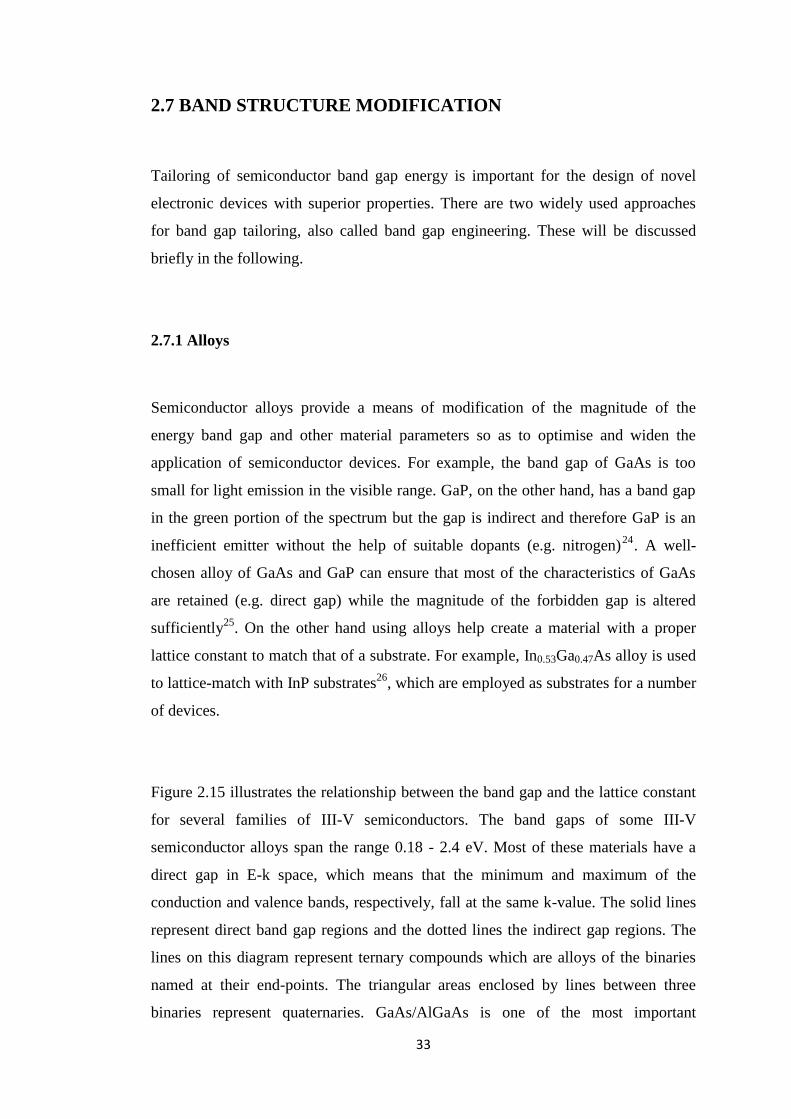
33
2.7 BAND STRUCTURE MODIFICATION
Tailoring of semiconductor band gap energy is important for the design of novel
electronic devices with superior properties. There are two widely used approaches
for band gap tailoring, also called band gap engineering. These will be discussed
briefly in the following.
2.7.1 Alloys
Semiconductor alloys provide a means of modification of the magnitude of the
energy band gap and other material parameters so as to optimise and widen the
application of semiconductor devices. For example, the band gap of GaAs is too
small for light emission in the visible range. GaP, on the other hand, has a band gap
in the green portion of the spectrum but the gap is indirect and therefore GaP is an
inefficient emitter without the help of suitable dopants (e.g. nitrogen)24
. A well-
chosen alloy of GaAs and GaP can ensure that most of the characteristics of GaAs
are retained (e.g. direct gap) while the magnitude of the forbidden gap is altered
sufficiently25
. On the other hand using alloys help create a material with a proper
lattice constant to match that of a substrate. For example, In0.53Ga0.47As alloy is used
to lattice-match with InP substrates26
, which are employed as substrates for a number
of devices.
Figure 2.15 illustrates the relationship between the band gap and the lattice constant
for several families of III-V semiconductors. The band gaps of some III-V
semiconductor alloys span the range 0.18 - 2.4 eV. Most of these materials have a
direct gap in E-k space, which means that the minimum and maximum of the
conduction and valence bands, respectively, fall at the same k-value. The solid lines
represent direct band gap regions and the dotted lines the indirect gap regions. The
lines on this diagram represent ternary compounds which are alloys of the binaries
named at their end-points. The triangular areas enclosed by lines between three
binaries represent quaternaries. GaAs/AlGaAs is one of the most important

34
heterostructure for device applications. The substitution of Al for Ga in GaAs does
not change the lattice constant appreciably (see Figure 2.15). This means that any
alloy of AlxGa1xAs grown on GaAs substrate, will be lattice matched, and therefore
no misfit dislocations or other structural defects should form. This fact made
GaAlAs/GaAs heterojunction lasers emerge as the first notable example of a new
generation of optoelectronic devices based on semiconductor alloys.
Figure 2.15: Band gap energy versus lattice constant of various III-V
semiconductors at room temperature27
.
Vegard’s law is an approximate empirical rule that describes a linear relation
between the crystal lattice constant of an alloy and the concentrations of the
constituent elements at constant temperature28,29
. When an alloy AxB1−x is produced
by a random mixing of two elements (the concepts can be applied to ternary and
quaternary alloys as well) the lattice constant of the alloy is given by Vegard’s law:
(1 )alloy A Ba xa x a 2.21
The change in the energy gap of the resulting alloy can be given by:
(1 )alloy B A
g g gE x E xE 2.22

35
However, in some alloys, there is a bowing influence arising from the increasing
disorder due to the alloying. So equation (2.22) is slightly changed by including the
bowing parameter (b).
(1 ) (1 )alloy B A
g g gE x E xE bx x 2.23
Alloys are usually divided into three categories depending on the arrangement of
their constituent atoms A and B.
1) Phase separated or clustered: if atom B is localized in a region different from the
region which atom A is localized (Figure 2.16-a)
2) Superlattice or ordered: if A and B atom form well defined periodic structures
(Figure 2.16-b)
3) Random alloy: no specific order (Figure 2.16-c)
Figure 2.16: A schematic example of (a) a clustered, (b) an ordered, and (c) a
random alloy.

36
Figure 2.17 shows the lattice constants versus mole fraction (x) for some important
alloys27
.
Figure 2.17: Lattice constant as a function of composition for ternary III-V
semiconductors. All cases obey Vegard’s law. The dashed lines show regions where
miscibility gaps are expected27
.
2.7.2 Heterostructures
A heterostructure is obtained by the junction of two different crystalline
semiconductors. The constituent materials of the heterojunction have different
energy band gaps, atomic size or lattice parameters. Heterostructures offer the
opportunity to manipulate the behaviour of the electrons and holes through band
engineering. The use of heterojunctions, based on III-V semiconductor alloys, in the
design and fabrication of semiconductor devices has led to the development of new
structures with improved performance. One important parameter for the formation of
heterojunctions is the band alignment between two semiconductor materials.
Heterojunctions can be classified based on how the energy bands align with respect
InAsxSb1-x
GaAsxSb1-x
InSb
0.64
0.62 AlSb GaSb
InAs
0.60
InP
0.58
AlAs, GaAs
0.56
AlP,GaP 0.54
AlxGa1-xP
AlxGa1-xAs
GaxIn1-xAs AlxAs1-xSb
GaxIn1-xSb
Mole Fraction (x)
Lat
tice
Co
nst
ant
, a
(nm
)
0 0.1 0.2 0.3 0.4 0.5 0.6 0.7 0.8 0.9 1.0
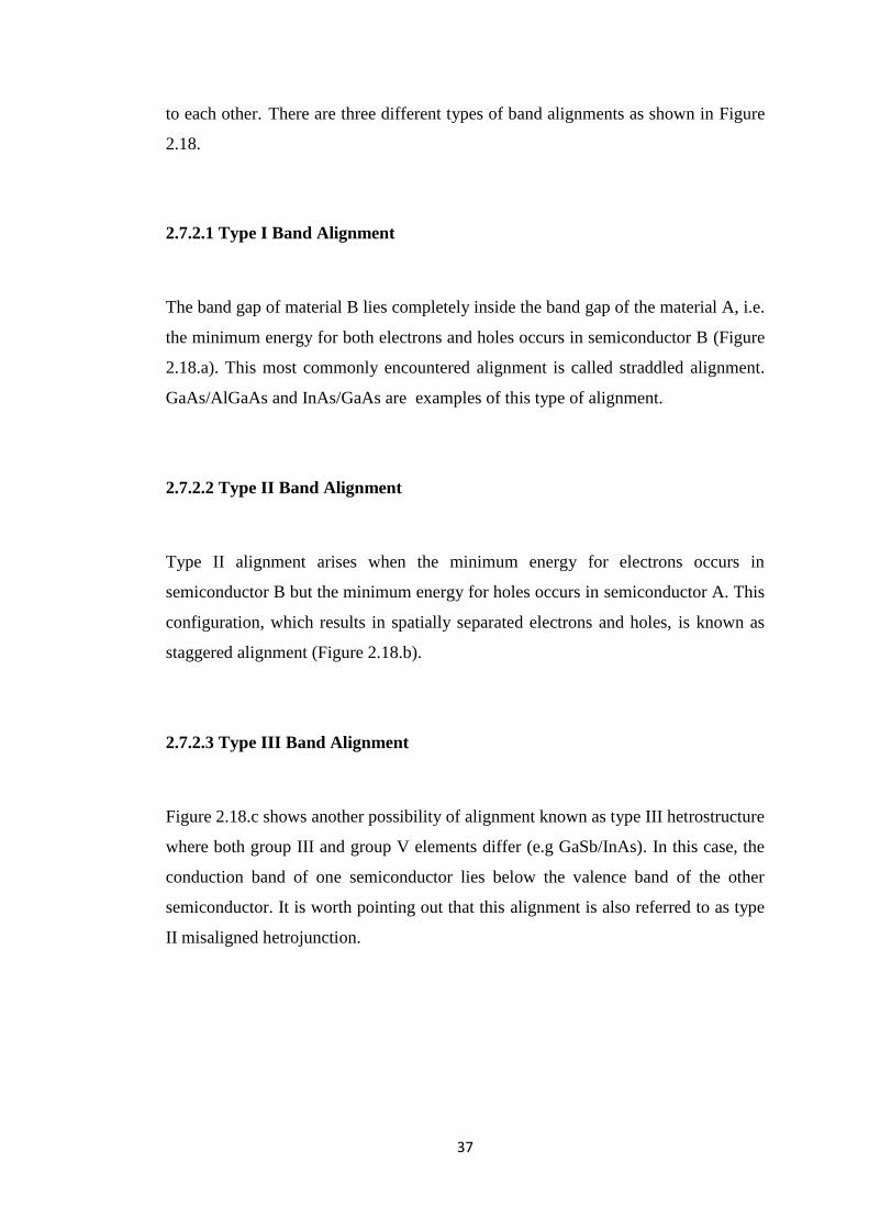
37
to each other. There are three different types of band alignments as shown in Figure
2.18.
2.7.2.1 Type I Band Alignment
The band gap of material B lies completely inside the band gap of the material A, i.e.
the minimum energy for both electrons and holes occurs in semiconductor B (Figure
2.18.a). This most commonly encountered alignment is called straddled alignment.
GaAs/AlGaAs and InAs/GaAs are examples of this type of alignment.
2.7.2.2 Type II Band Alignment
Type II alignment arises when the minimum energy for electrons occurs in
semiconductor B but the minimum energy for holes occurs in semiconductor A. This
configuration, which results in spatially separated electrons and holes, is known as
staggered alignment (Figure 2.18.b).
2.7.2.3 Type III Band Alignment
Figure 2.18.c shows another possibility of alignment known as type III hetrostructure
where both group III and group V elements differ (e.g GaSb/InAs). In this case, the
conduction band of one semiconductor lies below the valence band of the other
semiconductor. It is worth pointing out that this alignment is also referred to as type
II misaligned hetrojunction.

38
Figure 2.18: Classification of heterojunctions according to their band alignment,
where EC, EV, Eg, ΔEC, and ΔEV are the conduction band, valence band, energy gap,
conduction band offset, and valence band of the materials, respectively.
2.7.2.4 Anderson’s rule
In 1962 Anderson30
proposed the electron affinity model to calculate the band offset
of an ideal heterostructure. Electron affinity is defined as the energy difference
between the vacuum level and the bottom of the conduction band.
Consider two semiconductors which are brought into physical contact. The two
semiconductors are assumed to have an electron affinity of A and
B , and band
gap energy of g
AE and g
BE , respectively, as illustrated in Figure 2.19. The electron
affinity model is based on the fact that the energy balance of electron, moved from
the vacuum level to semiconductor A, then to semiconductor B, and finally to the
vacuum level, must be zero. This is given by:
0A C BE 2.24
or

39
C A BE
2.25
The valence band discontinuity follows automatically as
g
A B
V g CE E E E 2.26
The electron affinity rule is reasonably valid for some semiconductor pairs but it
fails for many other materials. One of the basic reasons for its failure is the chemical
character of the bonds in the adjacent material. For example by using this rule, the
theoretical value of the band offset of the AlAs/GaAs heterostructure is 230 meV
while the experimental value for this is near 530 meV. Kroemer31
explained the
failure of Andreson model by the formation of the semiconductor surface dipoles.
These dipoles, which are formed due to the readjustments of the atoms at the
semiconductor surface, affect the values of the electron affinity, and consequently
the band offset of the heterostructures.
Figure 2.19: Band diagram of (a) two separated semiconductors and (b) two
semiconductors in contact. The semiconductors have a band gap energy g
AE and
g
BE and an electron affinity of A and B .
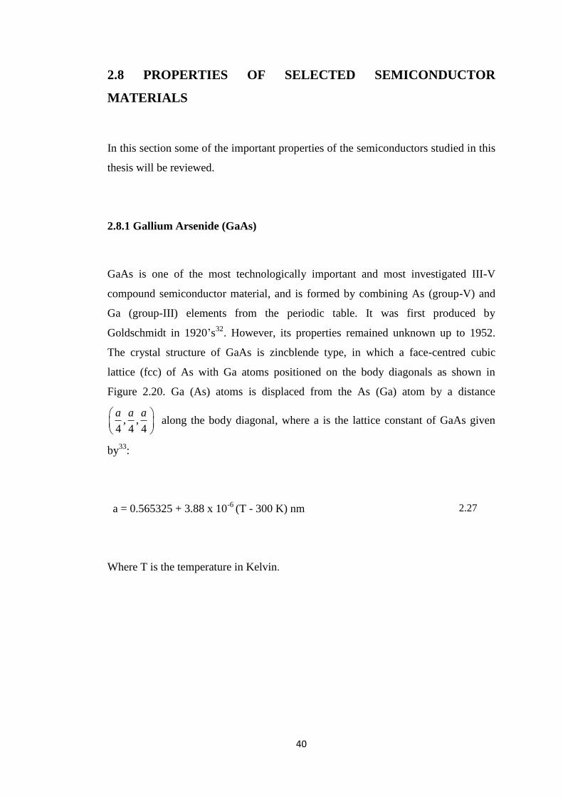
40
2.8 PROPERTIES OF SELECTED SEMICONDUCTOR
MATERIALS
In this section some of the important properties of the semiconductors studied in this
thesis will be reviewed.
2.8.1 Gallium Arsenide (GaAs)
GaAs is one of the most technologically important and most investigated III-V
compound semiconductor material, and is formed by combining As (group-V) and
Ga (group-III) elements from the periodic table. It was first produced by
Goldschmidt in 1920’s32
. However, its properties remained unknown up to 1952.
The crystal structure of GaAs is zincblende type, in which a face-centred cubic
lattice (fcc) of As with Ga atoms positioned on the body diagonals as shown in
Figure 2.20. Ga (As) atoms is displaced from the As (Ga) atom by a distance
, ,4 4 4
a a a
along the body diagonal, where a is the lattice constant of GaAs given
by33
:
a = 0.565325 + 3.88 x 10⁻⁶
(T - 300 K) nm
2.27
Where T is the temperature in Kelvin.

41
Figure 2.20: Conventional unit cube for GaAs.
Both the conduction band minima and the valence band maxima of GaAs lie at the
same value of wave vector at k = 0. Therefore, the transition of an electron from the
valence band to the conduction band doesn’t need phonon assistance. According to
the energy band diagram definition the nature of the GaAs band gap is direct. The
direct band gap ensures excellent optical properties of GaAs as well as superior
electron transport in the conduction band. This property makes GaAs superior over
Si, which has an indirect band gap, for devices used in optoelectronics applications.
Moreover, GaAs possesses higher carrier mobility than Si, and is preferably used in
high frequency devices. Electrical properties of GaAs material makes it suitable to
be used as a semi-insulating substrate for integrated circuits due to its high resistivity
compared to Si material. In addition, due to the fact that the energy gap of GaAs is
higher than that of Si, ( 1.424 1.1GaAs Si
g gE eV E eV at 300K), the GaAs devices
are more reliable to operate at higher temperatures than Si devices.
Figure 2.21 shows the band dispersion for increasing k along two different directions
of the Brillouin zone. The right hand side of the figure corresponds to moving from
the zone centre where k = (0,0,0) along the (001) direction to the zone edge at k =
(1,0,0). The left hand side corresponds to moving from k = 0 along the body
diagonal direction until reaching the zone edge at k =
(1,1,1). The single conduction
band corresponds to the (S) antibonding state. The three bands in the valence band
correspond to the three bonding orbitals, namely heavy hole (HH), light hole (LH),
and split off (SO) bands. Due to the large spin–orbit splitting, for most purposes, the
SO band does not play any role in electronic or optoelectronic properties. Hole
masses are m∗HH = 0.45m0; m∗LH = 0.08m0.

42
Figure 2.21: Diagram of the band structure in the vicinity of the energy gap of
GaAs: (a) throughout the first Brillouin zone, (b) a magnified view near the zone
center34
.
2.8.2 Aluminium Gallium Arsenide (AlGaAs)
The alloy AlxGa1-xAs has the same crystal structure as that of GaAs, except that a
fraction x of Ga atoms have been replaced by Al atoms. The incorporation of Al into
GaAs, which has the effect of increasing the band gap energy at 300 K from 1.42 eV
(GaAs) for x = 0 to 2.168 eV (AlAs) for x = 1, extend the range of applications from
near infrared to visible region. The energy change of the different conduction valleys
(X, Γ, and L) at 300K as a function of Al content (x) is shown in Figure 2.22.

43
Figure 2.22: Variation of the conduction band valleys in AlxGa1-xAs as a function of
Al composition (x) at 300 K35
.
In addition, it is worth pointing out that for Al content ≥ 0.44 the transition from
direct to indirect band gap takes place for AlGaAs material. The properties of
AlxGa1-xAs crystal are somewhat between those of GaAs and AlAs. The lattice
constant, a, of AlxGa1-xAs is given, to a first approximation, by linearly interpolating
the lattice constants of AlAs and GaAs. For example, the room temperature lattice
constant of AlxGa1-xAs as a function of the aluminium fraction x is given by:
a (x) = (0.56533 + 0.00078x) nm 2.28
The difference in the lattice constant, a, between x = 0 and x = 1 (i.e. between the
GaAs and AlAs crystals) is not more than 0.01a. Hence the interfaces between GaAs
and (AlGa)As can be made extremely smooth. This lattice match condition gives

44
significant reduction in defects, which is very important for good device
performance.
Besides the above mentioned selected properties, some other important properties of
intrinsic GaAs, and AlGaAs at room temperature are given in Table 2.4.
Table 2.4: Some important properties of intrinsic GaAs, AlAs and AlGaAs at 300K;
HH and LH stand for heavy hole and light hole, respectively36,37
.
Parameter GaAs AlAs AlxGa1-xAs
Crystal Structure Zincblende Zincblende Zincblende
Lattice constant (Å) 5.6533 5.6611 5.6533 + 0.0078x
Crystal density
(g/cm3)
5.360 3.760 5.360 - 1.6x
Energy band gap
(eV) at 300K
1.42 2.168 For x<0.45 (1.424+1.247x )
For x>0.45 ( 1.9+0.125x+
0.143x2)
Band type Direct Direct Changes from direct to indirect
for Al >0.45 content
Electron effective
mass
0.063 m0 0.150 m0 0.063+0.083x mo (x<0.45)
Hole effective mass 0.62m0 (HH)
0.087m0(LH)
0.76m0
(HH)
0.15 m0
(LH)
0.62 + 0.14x (HH)
0.087 + 0.063x (LH)
Dielectric constant
(static)
12.85 10.06 12.85-2.84x

45
Specific heat
(cal/g.K)
0.08 0.11 0.08+0.03x
Electron affinity
(eV)
4.07 3.4 4.07-1.1x (0<x<0.45)
3.46-0.14x (0.45<x<1)
2.8.3 Dilute Nitride Alloys
In 1992 Weyers et al38
made an interesting finding of a substantial reduction in the
band gap energy of GaAs semiconductor when the group V anions are partially
substituted by low concentration of highly electronegative N atoms. This reduction
in the band gap energy behaviour was further explored by Kondow et al39
.
Nitrogen causes a giant band gap bowing and tends to stretch and compress the
neighbouring bonds. Moreover a small amount of N in III-V material systems
produces an increase in the effective mass (meff). This behavior is in contrast to the
conventional semiconductors, where meff normally exhibits a decrease with reduction
in the band gap energy.
The general reason for the reduction in the GaAs band gap and other associated
effects is the presence of N-related localized states near the conduction band edge
the incorporation of N produce a significant local potential due to large differences
in atom size and electronegativity of N atoms and host anions40
.
Many of these effects can be explained by the simple two-level band anticrossing
(BAC) model41
. The (BAC) model in which the extended conduction band (CB)
states of GaAs admix and hybridize with the localized N-level above the CB edge, is
described briefly below.
The BAC model has predicted many interesting effects, such as an enhancement of
donor-binding42
energy and an electron effective mass43
due to N incorporation in
GaAs lattice, which have been experimentally proved. The BAC model describes the
electronic structure of N-alloys in terms of an interaction between the localized state
of nitrogen and the extended conduction band states of the host semiconductor
matrix44,45
, which results in splitting of the conduction band into the E- and E+

46
bands, and a reduction of the fundamental band gap. The E+ transition is shifted to
higher energy and the E- transition is shifted to lower energy from the N resonant
level with increasing N concentration. The energy difference between them increases
with increasing N concentration. Figure 2.23 shows the anticrossing behavior
between the N-related state (EN) and conduction band edge (ECB) of GaAs. The N-
related states are spread over the reciprocal space with constant energy because of its
localised nature. These two energy states are represented in Figure 2.23 by dotted
lines. According to the BAC model:
2 2
,
1( ) 4
2N CB N CB CB NE E E k E E V
2.29
Where ECB (k) and EN are the energies of the GaAs conduction band host matrix and
nitrogen state, respectively, and VCB,N is the matrix element describing the
interaction between the localized N states and extended CB states,
If one assumes that VCB,N is independent of k near the CB edge, then VCB,N can be
written as:
VCB,N=CN . x½ 2.30
Where CN is a constant which depends on the host matrix and x is the mole fraction
of substitutional N. Therefore equation 2.29 can be written as:
2 21( ) 4
2N CB N CB NE E E Ck E xE
2.31

47
Figure 2.23: Schematic diagram of band anticrossing model of GaAsN. Solid lines:
calculated dispersion relation for E± subbands of GaAs1-xNx using BAC model.
Dotted lines: unperturbed energies of the N level (EN) and the GaAs conduction
band.
The deficiency of the BAC model is that it is considered to work for single isovalent
impurity level and conduction band edge interaction and, it does not consider the
broadening of the energy levels or splitting of L-conduction band extreme. In spite of
all its shortcomings, it has been a popular and most cited model in dilute nitride
literature due to its simplicity and satisfactory fit to many characteristics of the alloy.
2.8.3.1 GaAsN Alloy
GaAsN was the first material system where reduction in the band gap as well as
lattice parameter was reported with the introduction of a small concentration of N.
The reduction of the band gap energy can be approximated by the empirical
relationship49
is given by:
EGaAs1-xNx(x) = EGaAs – (12x) eV
For x <0.015 2.32
In addition, as demonstrated by absorption measurement46-48
the nature of the band
gap of GaNxAs1-x alloy is direct. Moreover, according to numerous spectroscopic
Wavevector, K
Ener
gy
E+ (k)
E- (k)
EN
ECB (k)

48
studies PL polarization49
, time resolved PL spectroscopy50
and optically detected
cyclotron resonance (ODCR)51
the band alignment of GaAsN/GaAs hetrostructure
system is of type I.
A different set of values of the electron effective mass of the fluctuating from me* ~
0.8m0 to 0.1m0 has been reported in dilute nitrides materials52-57
. For example me*
has been found to increase from the GaAs host mass of 0.065 m058
up to 0.19 m0
with N~ 2%. The trend of the increase of the effective mass value with N% is
consistent with the BAC model. An electron effective mass of 0.11m0 for x~1.6%
has been the most acceptable value to date59
.
2.8.3.2 GaInAsN Alloy
The large difference in electronegativity and lattice constant between GaAs and GaN
results in large optical bowing coefficient60
and significant band gap reduction
following incorporation of small N concentration in the material. Moreover, in the
GaInNAs/GaAs system, reduction in the GaInNAs band gap contributes to a large
conduction band offset. Furthermore, incorporating N in GaInAs can compensate for
the compressive strain due to In, and result in GaInNAs lattice-matched to GaAs
substrate. For these reasons, the GaInNAs/GaAs system has been shown61-63
to be the
new key material system for long wavelength applications. The alloy Ga(1-
x)InxNyAs(1-y) is exactly lattice matched to GaAs when y = 0.35x.
2.9 OPTICAL PROPERTIES OF SEMICONDUCTORS
The wide-ranging optical properties observed in semiconductor materials can be
classified into a number of general phenomena, namely scattering, reflection,
transmission through the material or absorption in the material. If the incident
photons on a semiconductor have sufficient energy, they can excite an electron from
valence band to conduction band. The Created electron and hole pair may interact
with the lattice vibrations and the electrons of localized defects. As a result, the

49
optical spectra of the semiconductor provide a rich source of information about the
properties of the material.
2.9.1 Absorption Processes
The illumination of a semiconductor with photons of energy greater than the band
gap energy generates an electron-hole pair by the optical process. In this case, a
photon excites an electron from the filled valence band to the empty conduction band
as shown in Figure 2.24 By applying the law of conservation of energy to the
interband transition the following relationship holds:
f iE E 2.33
Where Ei is the energy of the initial state in the lower band, Ef is the energy of the
final state in the upper band, and ħω is the photon energy. In bulk semiconductors
there is a continuous range of energy states within the upper and lower bands, and
therefore the interband transitions will be possible over a continuous range of
frequencies. The range of frequencies is determined by the upper and lower energy
limits of the bands. Interband transitions therefore give rise to a continuous
absorption spectrum from the low energy threshold at Eg to an upper value set.

50
Figure 2.24: Interband optical absorption between an initial state of energy Ei in an
occupied lower band and a final state at energy Ef in an upper band. The energy
difference between the two bands is Eg.
The absorption spectrum of a given material is related to its band structure and in
particular to the density of states for the transition. From the classical point of view,
for the direct band gap semiconductors such as GaAs, the absorption coefficient (α)
as a function of wavelength (λ) can be expressed as:
1
2( ) gA E ħ 2.34
Where constant A depends upon the material properties, Eg is the energy gap and ħω
is the incident photon energy. Figure 2.25 illustrates the absorption coefficient of Si
and GaAs as a function of the energy of the incident light.

51
Figure 2.25: absorption coefficient as a function of energy of incident light of GaAs
and silicon near their band edges64
. Note that the vertical axis is logarithmic.
Semi classically, absorption is determined by the quantum mechanically transition
rate Wi→f for exciting an electron in an initial quantum state ψi to a final state ψf by
absorption of a photon of angular frequency ω. The transition rate is given by the
Fermi’s golden rule:
22( )i FW M g
2.35
The transition rate thus depends on two factors:
1- The matrix element M
2- The density of state g(ħω)
The matrix element M, which describes the interaction between photons and
electrons, is given by:
( ) ( )
*3
( ) ( )f r i rr rM f H i H d 2.36
Where the limits of the integration are over the whole crystal.
H' is the perturbation associated with the light wave, and r is the position vector of
the electron.

52
The electron states in a crystalline solid are described by Bloch functions. The wave
functions can be expressed as a product of a plane wave and an envelope function
that has the periodicity of the crystal lattice these are given by:
.1( ) ( ) iiK r
i ir U r eV
2.37
.1( ) ( ) fiK r
f fr U r eV
2.38
Where Uf and Ui are the appropriate envelope functions for the initial and final
bands, respectively, and V is the normalization volume, ki and kf are the wave
vectors of the initial and final electron states.
When photons are treated classically, the perturbation H' could be expressed as:
.e photonH P 2.39
Where Pe is the electron dipole moment caused by electric field Ɛ.
2.9.2 Photoluminescence
In this section the re-emission of photons by interband luminescence after the
semiconductor has been excited by a photon with energy greater than band gap (Eg)
will be considered. The physical processes involved in photoluminescence are more
complicated than those in absorption. This is because the generation of light by
luminescence is intimately tied up with the energy relaxation mechanisms in the
solid. The shape of the emission spectrum is affected by the thermal distributions of
the electrons and holes within their bands.
In a photoluminescence experiment, a quantum of light (photon) from a laser is
absorbed by an electron, thus making a transition from the valence band to the

53
conduction band. This produces a hole in the valence band. Following this optical
excitation, electrons and holes undergo spatial and temporal evolution with
characteristic times which depend on the various relaxation processes (see Table 2.5
and Figure 2.26) 65
.
Table 2.5: Fundamental processes in semiconductors.
Microscopic process Characteristic time (sec)
Carrier-carrier scattering 10-15
-10-12
Intervalley scattering 10-14
Intravalley scattering 10-13
Carrier-optical phonon thermalization 10-12
Optical phonon-acoustic phonon interaction 10-11
Carrier diffusion 10-11
Auger recombination ( when carrier density > 1020
cm-3
) 10-10
Radiative recombination 10-9
Lattice heat diffusion 10-8
Figure 2.26: Photoluminescence in a solid. Incoming photons with energy higher
than the band gap energy excite an electron from ground state to excited state.
Electron relaxes to the lowest available level before dropping down to empty levels
in the ground state band by emitting a photon.
Eg i gE
relaxation
Valence band
Conduction band
Ground state
Excited state
RNR

54
The spontaneous emission rate for radiative transitions between two levels (see
Figure 2. 27) is determined by the Einstein coefficient A as given below.
1
R
A
2.40
R is the natural radiative lifetime of the excited sate
If the upper level has a population N at time t, the radiative emission rate is given by:
radiativedN
ANdt
2.41
This rate equation can be solved to give:
( ) (0)exp( ) (0)exp( )R
tN t N At N
2.42
The Einstein A coefficient is directly proportional to the B coefficient66
, which
determines the absorption probability.
3
3
8 hA B
c
2.43
This relationship tells us that transitions that have a high absorption probability will
also have a high emission probability.

55
Figure 2. 27: Absorption,and spontaneous emission transitions between two levels
of an atom in the presence of electromagnetic radiation.
The relationships between the A and B Einstein coefficients given in equation 2.41
have been derived for the case of an atom in equilibrium with black body radiation.
The luminescence intensity (I) at frequency (ν) can be written as:
2( ) ( )I h M g h x Level occupancy factor 2.44
Where the occupancy factor gives the probabilities that the relevant upper level is
occupied and the lower level is empty.
The occupancy conditions for photon emission between the discrete energy levels E2
and E1 are stated as follows: a conduction-band state of energy E2 is filled (with an
electron) and a valence-band state of energy E 1 is emptied (i.e., filled with a hole).
The probabilities that these occupancy conditions are satisfied for various values of
E 2 and E 1 are determined from the appropriate Fermi functions fc and fv associated
with the conduction and valence bands. The probability fe(ν) that the emission
condition is satisfied for a photon of energy hν is the product of the probabilities that
the upper state is filled and that the lower state is empty (these are independent
events), i.e.,

56
2 1( ) ( ) 1 ( )e c vf f E f E 2.45
The other two terms are the matrix element (M) and the density of states (g) for the
transition, which determine the quantum mechanical transition probability by Fermi's
golden rule (equation 2.35).
The light is emitted between the electron and hole states that are thermally occupied
(electrons and holes are thermally distributed within kT after their relaxation to their
respective bands), and will therefore only be emitted within a narrow energy range
from the lowest levels in the excited state band. This contrasts with the absorption
spectrum, where photons can be absorbed to any state within the excited state band,
no matter how far it is above the bottom of the band.
Radiative emission is not the only mechanism by which the electrons in an excited
state can drop down to the ground state. The electron might, for example, lose its
energy as heat by emitting phonons, or it may transfer the energy to impurities or
defects called 'traps'. If these non-radiative relaxation processes occur on a faster
time scale than the radiative transitions, then a very small number of photons will be
emitted.
The luminescence efficiency R in this case is given by:
1
1R
R
NR
2.46
Where R , and NR are the radiative and non-radiative lifetimes, respectively.
If R >> NR then R is very small and the light emission is very inefficient. Thus
efficient luminescence requires that the radiative lifetime should be much shorter
than the non-radiative lifetime.

57
REFERENCES
1 L. Coldren, S. Corzine, M. Mashanovitch, Diode Lasers and Photonic Integrated
Circuits, (Wiley Series in Microwave and Optical Engineering (1995).
2 S. M. Sze, and K. K. Ng, “Physics of Semiconductor Devices”. 3rd ed.: Wiley-
Interscience, A John Wiley & Sons, Inc, Publication (2007).
3 M. Henini, P. J. Rodgers, P. A. Crump, B. L. Gallagher, and G. Hill, Applied
Physics Letters, 65, 2054, (1994).
4 A. Polimeni, M. Henini, A. Patanè, L. Eaves, P. C. Main, and G. Hill, Applied
Physics Letters, 73, 1415 (1998).
5 A. Patanè, A. Levin, A. Polimeni, F. Schindler, P. C. Main, L. Eaves, and M.
Henini, Applied Physics Letters, 77, 2979, (2000).
6 K. Wang, K. Edmonds, L. Zhao, M. Sawicki, R. Campion, B. Gallagher, and C.
Foxon, Physical Review B, 72, 115207 (2005).
7 M.Henini, Ill-Vs Review, 11 (3), 48 (1998).
8 H. Xu, Q. Gong, B. Xu, W. Jiang, J. Wang,W. Zhou, Z. Wang, Journal of Crystal
Growth, 200, 70 (1999).
9 M. Henini, Nanoscale Research Letters, 1, 32 (2006).
10 Y. Temko, T. Suzuki, P. Kratzer, and K. Jacobi, Physical Review B, 68, 165310
(2003).
11 T. Suzuki, Y. Temko, and K. Jacobi, Applied Physics Letters, 80, 4744 (2002).
12 K. Jacobi, Progress in Surface Science, 71, 185 (2003).

58
13 D. Lubyshev, P. Gonzalez-Borrero, E. Marega, E. Petitprez, and P. Basmaji,
Journal of Vacuum Science & Technology B, 14, 2212 (1996).
14 M. Xu, Y. Temko, T. Suzuki, and K. Jacobi, Physical Review B, 71, 075314
(2005).
15 M. Xu, Y. Temko, T. Suzuki, and K. Jacobi, Surface Science, 576, 89 (2005).
16 K. Longenbach , and W. Wang, Applied Physics Letters, 59, 2427 (1991).
17 P. Vaccaro, M. Hirai, K. Fujita, T. Watanabe, Journal of Physics D: Applied
Physics, 29, 2221 (1996).
18 R. Notzel, Semiconductor Science and Technology, 11, 1365 (1996).
19 D. Kovalev, H. Heckler, G.Polisski, and F. Koch, Physica Status Solidi B, 215,
871, (1999).
20 P. Zhao, D. Hu, and X. Wu, Chinese Physics Letters, 22, 1492 (2005).
21 M. Tabe, M. Kumezawa,Y. Ishikawa, and T. Mizuno, Applied Surface Science,
175, 613 (2001).
22 S. Ding, M. Ikeda, M. Fukuda, S. Miyazaki, and M. Hirose, Applied Physics
Letters, 73, 3881 (1998).
23 Y. Varshni, Physica , 34, 149 (1967).
24 M. Jaros, Reports on Progress in Physics, 48, 1091 (1985).
25 A. Bergh, and P. Dean, Light Emitting Diodes (Oxford: Clarendon) (1976).

59
26
J. Bahk, Z. Bian, M. Zebarjadi, J. Zide, H. Lu, D. Xu, J. Feser, G. Zeng, A.
Majumdar, Arthur C. Gossard, A. Shakouri, and J. Bowers, Physical Review B, 81,
235209 (2010).
27 Jasprit Singh “Electronic and Optoelectronic Properties of Semiconductor
Structures”, Cambridge University Press (2003).
28 L. Vegard, Die Konstitution Der Mischkristalle Und Die Raumfüllung Der Atome,
Zeitschrift Für Physik, 5, 17 (1921).
29 A. Denton, and N. Ashcroft, Physical Review A, 43, 3161 (1991).
30 R. Anderson, “Germanium-Gallium Arsenide Heterojunction” IBM Journal of
Research and Development, 4(3), 283(1960).
31 H. Kroemer, Reviews of Modern Physics, 73, 783 (2001).
32 J. D. Bernal, M. A., F. “The Goldschmidt Memorial Lecture”. Journal of the
Chemical Society (Resumed), 1929 Republished 1949: p. 2108. V. M. B.
Goldschmidt, J. D, The Goldschmidt Memorial Lecture. Journal of the Chemical
Society (Resumed), 1929 Republished 1949: p. 7.
33 Richard John Allan Hill, Tunnelling into InAs Quantum Dots (Nottingham
university, PhD Thesis)
34 M. Fox, optical properties of solids, Oxford University Press Inc., New York
(2001).
35 John. Davies, The physics of low-dimensional semiconductors an introduction,
Cambridge University Press (1998).
36 J. Blakemore, Journal of Applied Physics, 53, R123 (1982).

60
37
S. Adachi, Journal of Applied Physics, 58, R1 (1985).
38 M. Weyers, M. Sato, H. Ando, Japanese Journal of Applied Physics, 31, L853
(1992).
39 M. Kondow, K. Uomi, K. Hosomi, T. Mozume, Japanese Journal of Applied
Physics, 33, L1056 (1994).
40 H. P. Hjalmarson, P. Vogl, D. J. Wolford, and J. D. Dow, Physical Review Letters,
44, 810 (1980).
41 W. Shan, W. Walukiewicz, J. W. Ager III, E. E. Haller, J. F. Geisz, D. J.
Friedman, and J. M. Olson and S. R. Kurtz, Physical Review Letters, 82,
1221(1999).
42 K. M. Yu, W. Walukiewicz, W. Shan, J. W. Ager, III, J. Wu, E. E. Haller, J. F.
Geisz, D. J. Friedman, and J. M. Olson, Physical Review B, 61, R13337 (2000).
43 J. Geisz, D. Friedman, J. Olson, S. Kurtz, B. Keyes, Journal of Crystal Growth,
195, 401 (1998).
44 A. Lindsay, and E. P. O’Reilly, Solid State Communications, 112, 443(1999).
45 W. Shan, W. Walukiewicz, J. W. Ager, E. E. Haller, J.F. Geisz, D. J. Friedman, J.
M. Olsonand, and S. R. Kurtz, Physical Review Letters, 82, 1221(1999).
46 M. Weyers, M. Sato, H. Ando, Japanese Journal of Applied Physics, 31, L853
(1992).
47 W. G. Bi, C. W Tu, Applied Physics Letters, 70, 1608, (1997).
48 M. Kondow, K. Uomi, K. Hosomi, T. Mozume, Japanese Journal of Applied
Physics, 33, L1056 (1994).

61
49 Y. Zhang, A. Mascarenhas, H. P. Xin, C. W. Tu, Physical Review B, 61, 4433
(2000).
50 A. Buyanova, G. Pozina, P. N. Hai, W. M. Chen, H. P. Xin, C. W. Tu, Physical
Review B, 63, 033303 (2001).
51 P. N. Hai, W. M. Chen, I. A. Buyanova, H. P. Xin, C. W. Tu, Applied Physics
Letters, 77, 1843 (2000).
52 M. Hetterich, M. D. Dawson, A. Yu. Egorov, D. Berklau and H. Riechert, Applied
Physics Letters, 76, 1030 (2000).
53 Z. Pan, L. H. Li, Y. W. Lin, B. Q. Sun, D. S. Jiang and W. K. Ge, Applied Physics
Letters, 78, 2217 (2001).
54 R. Mouillet, L. A. de Vaulchier, E. Deleporte, Y. Guldner, L. Travers and J. C.
Harmand, Solid State Communications, 126, 333 (2003).
55 M. Kondow, S. Fujisaki, S. Shirakata, T. Ikari and T. Kitatani, International
Symposium on Compound Semiconductors‟, San Diego, CA76 (2003).
56 C. Skierbiszewski, Semiconductor Science and Technology, 17, 803 (2002).
57 J. B. Heroux, X. Yang, and W. I. Wang, Journal of Applied Physics, 92, 4361
(2002).
58 P. N. Hai, W. M. Chen, I. A. Buyanova, H. P. Xin, C. W. Tu, Applied Physics
Letters, 77, 1843 (2000).
59 J. Wu, W. Shan,W. Walukiewicz, K. M. Yu, J. W. Ager III, E. E. Haller, H. P.
Xin, C.W. Tu, Physical Review B, 64, 085320, (2001).
62
60
S. Wei, and A. Zunger, Physical Review Letters, 76, 664 (1996).
61 M. Kondow, K. Uomi, A. Niwa, T. Kitatani, S. Watahiki, Y. Yazawa, Japanese
Journal of Applied Physics, 35, 1273 (1996).
62 T. Miyamoto, K. Takeuchi, F. Koyama, K. Iga, IEEE Photonics Technology
Letters, 9, 1448 (1997).
63 M. Fischer, M. Reinhardt, A. Forchel, Electronics Letters, 36, 1208 (2000).
64 E. D Palik, Handbook of the optical constants of solids. Academic Press, San
Diego (1985).
65 J.Shah, Solid state Electron, 21, 43,(1978).
66 M. Fox, Appendix B, optical properties of solids, Oxford University Press Inc.,
New York (2001).

63
CHAPTER 3: THE GROWTH AND OPTICAL
PROPERTIES OF LOW DIMENSIONAL
SEMICONDUCTOR STRUCTURES
64
In this chapter the fundamental concepts of low dimensional semiconductor
structures will be presented including their fabrication and properties which form a
key aspect to understanding the optical studies of quantum dots and quantum wells
investigated in this work
3.1 INTRODUCTION
Low dimensional semiconductor structures (LDSS) form a major new field of
physics research. They are semiconductor structures which have a small scale in one,
two or three spatial dimensions. Their electronic and optical properties, as compared
to the same material in bulk form, are significantly changed by quantum confinement
effects. A typical example of such a structure, in which charge carries are confined to
move freely in only two dimensions, is a so-called quantum well. The interest in the
preparation, study and applications of LDSS has revitalised condensed matter science
and has increased worldwide. These advanced LDSS offer device engineers new design
opportunities to tailor novel electronic devices. Thin epitaxial layers with nanometer
size were first produced in the late 1970's and this allowed a surge in the study of
LDSS. The main requirements, which in practice will be dependent upon the precise
application being considered, for ideal LDSS are:
(1) Optical and structural quality: semiconductors produce light when an electron
in the conduction band recombines with a hole in the valence band – a
radiative process. However, the presence of defects which form energy states
within the band gap may weaken the light emission process since
recombination of electron – hole occur through this defect. If non-radiative
processes become major then the optical efficiency, i.e the number of
photons produced for each injected electron and hole, decreases. For
semiconductor laser applications, nanostructures with small defect numbers
are therefore required. Poor structural quality may also degrade the carrier
mobility.
(2) Size: for many applications the majority of electrons and holes should lie in
their lowest energy state, implying negligible thermal excitation to higher

65
states. The degree of thermal excitation is determined by the ratio of the
energy separation of the confined states and the thermal energy kBT, where
KB is the Boltzman constant and T is the temperature. At room temperature
kBT ~ 25 meV and as a rule of thumb the level separation should be at least
three times this value (i.e. ~75 meV). As the energy spacing between the
states is determined by the size of the structure, increasing the size of the
structure results in a decrease of the energy spacing between the confined
states. The above requirement sets an upper limit on the size of a
nanostructure.
(3) Uniformity: devices will typically contain a large number of nanostructures.
Ideally each nanostructure should have the same shape, size and composition.
(4) Growth compatibility: the epitaxial techniques of Molecular Beam Epitaxy
(MBE) and Metal-Organic Vapour Phase Epitaxy (MOVPE) are used for the
mass production of electronic and electro-optical devices. The commercial
exploitation of nanostructures will be more likely if they can be fabricated
using these techniques.
(5) Confinement potential: the potential wells confining electrons and holes in a
LDSS must be relatively deep. If this is not the case then at high temperatures
significant thermal excitation of carriers out of the nanostructure will occur.
For electrical applications it is generally sufficient for either electrons or
holes to be trapped or confined within the nanostructure. For electro-optical
applications it is necessary for both types of carrier to be confined.
(6) p-i-n structures: the ability to place a nanostructure within the intrinsic region
of a p-i-n structure allows the efficient injection or extraction of carriers.
3.2 QUANTUM CONFINEMENT
The nanostructured materials have unique optical and electronic properties that are
completely different from those of the bulk. The tunability of their optical properties
due to size variation allows many optoelectronic applications such as LED, lasers,
and photovoltaic devices. These unusual properties of semiconductor nanomaterials
are due to the so-called quantum confinement or quantum size effect.

66
The optical properties dependence on the size of the nanostructures is a consequence
of the quantum confinement effect. The Heisenberg uncertainty principle states that
if a particle is confined to a region of length Δx in the x axis, then an uncertainty is
introduced in its momentum, and is given by:
xP ~x
3.1
If the particle is otherwise free, and has a mass m, the confinement in the x direction
gives it an additional kinetic energy of magnitude
2( )
2
xconfinement
PE
m
~
2
22m x
3.2
This confinement energy will be important if it is equal to or greater than the kinetic
energy of the particle due to its thermal motion in the confinement direction.
This condition may be written as:
confinementE ~
2
22m x
> 1
2Bk T
3.3
The quantum size effects will become important if
2
B
xmk T
3.4
The criterion given in equation (3.4) provides an idea of how small the structure
must be if the quantum confinement effects are to be observed.
3.3 DENSITY OF STATES
The electronic and optical performance of a device is controlled by the density of
states (DOS), which is defined as the number of available electronic states per unit
volume per unit energy at an energy E. The DOS depends on the dimensionality of
the system and the energy versus the corresponding wave vector dispersion relation
for the particle. The dispersion relation for an electron in bulk material is given by:

67
3.5
Where are the effective mass of electron, wavevector number, and
Plank’s constant, respectively
For a three-dimensional (3D) bulk material, the DOS is defined as the number of
available electronic states per unit volume per unit energy at energy E and is given
by:
( ) √
⁄
⁄
3.6
Passing from three-dimensional bulk to two-dimensional (2D) structures, so called
‘quantum well’, the carrier movement is restricted to a plane. Such two-dimensional
systems include thin films, quantum wells and super lattices. In 2D systems the DOS
is modified with regards to the number of available electronic states per unit area per
unit energy and is given by:
( )
3.7
Further reduction in the dimensionality of the system leads to a ‘quantum wire’ or
one dimensional (1D) system. Examples of such 1D structure include nano tubes,
semiconductor nanowires, and nanorods. For a quantum wire the DOS is given by:
1
21/22
emD E E
п
ħ
3.8
For a zero dimensional (0D) system, such as a quantum dot (QD), the confinement is
along all three dimensions and the DOS becomes a delta function. The electron can
only have certain discrete energies in the quantum dot. The energy of the states and
the number of states available depends on the shape and size of the dot potential. For
a quantum dot the DOS is given by:
( ) ( )D E E Ec 3.9

68
Figure 3.1 demonstrate how the density of states in the conduction band changes
with the degree of confinement.
Figure 3.1: Density of states N(E) in the conduction band for (a) bulk semiconductor
(3D), (b) quantum well (2D), (c) quantum wire (1D), and quantum dot (0D).
3.4 OPTICAL PROCESSES IN LOW DIMENSIONAL
SEMICONDUCTOR STRUCTURES
In the following sections optical processes and carrier dynamics will be considered
only for the case of quantum wells and quantum dots.
3.4.1 ABSORPTION IN SEMICONDUCTOR NANOSTRUCTURES
Semiconductor can absorb a photon in a process where an electron is promoted
between the valence and conduction bands. The strength of this absorption is
proportional to the density of states in both bands – the joint density of states. The
joint density of states has a form similar to the density of states in both the
conduction and valence bands, and is therefore a strong function of the
dimensionality of the system. The absorption will be modified by the quantised
energy levels of a nanostructure, resulting in a number of different energy transitions
occurring between the confined hole and electron states. A further modification
Ec
D(E)
E Ec
D(E)
E E
D(E)
Ec E
D(E)
Ec
(a) (b) (c) (d)

69
arises from the influence of excitonic effects. Excitons are bound electron-hole pairs
held together by their mutual Coulomb attraction. Since the optical transition can be
considered as the creation of an electron-hole pair, the Coulomb attraction increases
the absorption rate because it enhances the probability of forming the electron-hole
pair. For an ideal two-dimensional system, the exciton binding energy is increased
by a factor of four compared to the bulk value. In a real quantum well the electron
and hole wave functions penetrate into the barriers, and the ideal two dimensional
case is never achieved. However, an approximately twofold enhancement can be
achieved. A larger binding energy decreases the probability of exciton ionisation at
high temperatures and, as a consequence, stronger excitonic effects are observed in a
nanostructure at room temperature than in a comparable bulk semiconductor. Figure
3.2 shows the absorption coefficient of a 40 period GaAs/AlAs multi-quantum wells
(MQWs) structure with 7.6 nm wide QWs at 6 K. The spectrum consists of a series
of steps, representing the density of states of a two dimensional system with an
excitonic enhancement at the onset of each step. A number of transitions are
observed between the confined hole state and confined electron state. These
transitions are subject to the selection rules. The enhancement of the excitonic
binding energy in the quantum well is a consequence of the quantum confinement of
the electrons and holes. This forces the electrons and holes to be closer together than
they would be in a bulk semiconductor, and hence increases the attractive potential.
One of the most useful consequences of the enhancement of the exciton binding
energy in quantum wells is that the excitons are still stable at room temperature. This
contrasts with bulk GaAs, which only shows strong excitonic effects at low
temperatures. This can be clearly seen in the data presented in Figure 3.3. The
enhancement of the excitonic strength in the QW, due to the increased exciton
binding energy, is clearly visible.

70
Figure 3.2: Low-temperature absorption spectrum of a 40-period GaAs/AlAs
multiple quantum well structure with 7.6 nm wide wells. The most intense features
result from transitions between the nth
(n = 1, 2, 3) confined light hole (lh) and heavy
(hh) hole states and identical index electron states. In addition, two weaker
transitions are observed between electron states (e1 and e3) and the first (hh1) and
third heavy hole (hh3) states, namely hh3 - e1 and hh1 - e31.
Figure 3.3: Room temperature absorption spectrum of a GaAs/Al0.28Ga0.72As MQW
structure containing 77 GaAs quantum wells of width 10 nm. The absorption
spectrum of bulk GaAs at the same temperature is shown for comparison2.

71
3.4.2 PHOTOLUMINESCENCE PROCESS IN NANOSTRUCTURES
Electrons and holes can be created in a semiconductor either optically with incident
photons of energy greater than the band gap, or by electrical injection in a p-n
junction. The electrons and holes are typically created with excess energies above
their respective band edges. However, the time required to lose this excess energy is
generally much shorter than the electron–hole recombination time. Consequently the
electron and holes relax to their respective band edges before recombining to emit a
photon. Emission therefore occurs at an energy corresponding to the band gap of the
structure, with a small distribution due to the thermal energies of the electrons and
holes. The influence of rapid carrier relaxation is demonstrated in the emission
spectrum of a structure containing quantum wells of five different widths (see Figure
3.4). Only emission corresponding to the lowest-energy transition of each well is
observed, even though the wider wells contain a number of confined states.
Figure 3.4: Emission spectrum of a quantum well structure containing five wells of
different thicknesses. The wells are Ga0.47In0.53As and the barriers are InP. The inset
shows the electronic structure and the nature of the optical transitions3.

72
Higher-energy transitions in a nanostructure can be observed in emission if the
density of electrons and holes is sufficiently large that the underlying electron and
hole states are populated. This can occur under high-excitation conditions where the
lower energy states become fully occupied and carriers are prevented from relaxing
into these states due to the Pauli Exclusion Principle. Figure 3.5 shows the emission
spectra of an ensemble of self-assembled quantum dots for different optical
excitation powers. At low powers the average number of electrons and holes in each
dot is very small, and consequently only the lowest-energy (ground state) transition
is observed. However, with increasing power the ground state, which has a
degeneracy of two, is fully occupied and emission from higher-energy (excited)
states are observed. Fluctuations in the size, shape and composition within an
ensemble of quantum dots result in a significant inhomogeneous broadening of the
optical spectra due to size non-uniformity of the quantum dots. However, by probing
a very small number of dots, the predicted very sharp emission from these 0D
nanostructures can be observed.
Figure 3.5: Emission spectra of an ensemble of InAs self-assembled quantum dots
for three different laser power densities. At the highest power, emission from three
different transitions is observed. The numbers by each spectrum indicate the relative
intensity scale factors4

73
3.5 EPITAXIAL GROWTH OF LOW DIMENSIONAL
SEMICONDUCTOR STRUCTURES
Epitaxy is a controlled way of growing a solid film on a crystalline substrate, in
which the atoms of the growing film adjust to the atomic arrangement of the
substrate atoms. The two main epitaxial methods used for growing low dimensional
semiconductor structures are molecular beam epitaxy (MBE) and metal-organic
vapour phase epitaxy (MOVPE). In MBE, the material to be deposited is evaporated
in ultra-high vacuum (UHV), where epilayers crystallise when the atoms hit the hot
substrate. Since MBE is operated under UHV condition, simultaneous
characterisation of the growing film is possible. This fact makes this method very
popular in research environments. However, the growth rate is very slow, which
limits the thickness of the film to be grown. MOVPE is a chemical method used to
grow semiconducting materials, which does not require as high vacuum as MBE and
the growth rate is in general much higher than in MBE. MOVPE is therefore a
preferred method to grow devices that require large thicknesses. To illustrate the
importance of low dimensional semiconductor structures in optoelectronic devices,
an example will be given to show the influence of confinement on the electronic
transitions and optical properties of a QW.
3.5.1 MOLECULAR BEAM EPITAXY
MBE5 is an epitaxial process involving the reaction of one or more thermal beams of
atoms or molecules with a crystalline surface under UHV conditions, typically of the
order of 5 x 10-11
mbar or better (atmospheric pressure is about 1000 mbar). MBE
can achieve precise control in both chemical compositions and doping profiles.
Single-crystal multilayer structures with dimensions on the order of atomic layers
can be made using MBE. Thus, the MBE method enables the precise fabrication of
semiconductor heterostructures having thin layers from a fraction of a micron down
to a monolayer. The disadvantage of MBE is that the growth process is slow.
Generally, the growth rate is about 1 µm per hour which translates to a rate of 1
monolayer per second. Advantages of MBE include highly abrupt junctions between

74
different materials, good control over the thickness of layers, good reproducibility,
and the ability to scale the process for mass production.
The elements that constitute a heterostructure (e.g. Ga, As, and Al, etc) are vaporized
in furnaces with orifices directed towards the substrate, but shielded from it by
shutters. This is the Knudsen or molecular-flow regime of a gas, and the furnaces are
called Knudsen or K-cells. Molecules that emerge from the K-cells do not diffuse as
in a gas but form a molecular beam; travelling in straight lines without collisions
until they impinge on the substrate (the mean free path of molecules between
collisions is much larger than the width of the chamber at UHV condition). The
substrate holder rotates continuously to achieve uniform epitaxial layers (e.g., ±1%
in doping variations and ±0.5% in thickness variations).The flux of each element can
be controlled through the temperature of each furnace. Growth starts when the
shutters are opened. Dopants are added by using additional cells. The usual donor is
Si, which belongs to group IV of the periodic table. However, it is not obvious
whether it should act as a donor or acceptor in a group III-V compound. This
depends on which host atom the Si will replace. Usually Si acts as a donor in
conventional (100) GaAs substrate, but it can also act as an acceptor by growing on a
different surface from the usual (100) orientation. It also tends to become
amphoteric, acting both as a donor and acceptor, at very high concentrations (around
10-25
m-3
). Beryllium element is commonly used as an acceptor in III-V
semiconductors.
3.5.2 GROWTH OF QUANTUM WELL STRUCTURES
A quantum well is a potential well within a semiconductor structure which is
adequately thin to confine the carrier’s movement on a length-scale similar to their
de Broglie wavelength which, for an electron in GaAs at room temperature, is about
30 nm. When carriers are localized in this way their electronic and optical properties
are determined by quantum mechanical aspects of their behaviour which are not
apparent in bulk structures. Figure 3.6 (a) shows a schematic diagram of the simplest
type of quantum well that can be grown. In this particular case, a GaAs/AlGaAs
structure is grown on a GaAs substrate. The structure consists of a GaAs layer of

75
thickness (d) sandwiched between much thicker layers of the alloy semiconductor
AlGaAs; d is chosen so that it is comparable to de Broglie wavelength.
GaAs/AlxGa1-xAs materials are unique among III-V semiconductors because the
dimensions of the crystalline lattice of GaAs and AlxGa1-xAs match within 0.1% for
all values of x. This property makes growth of GaAs/AlxGa1-xAs heterostructures
straightforward without any possible defect. The difference in bandgaps of the two
materials can vary at room temperature from 0 eV to as much as 1.6 eV (as x
increases from 0 to 1).
As Ga is substituted by Al in the AlxGa1-xAs alloy system the direct band gap
increases from 1.424 eV in GaAs (x = 0) to 3.018 eV in AlAs (x = 1). A quantum
well is formed using a narrow GaAs layer sandwiched between barrier layers of
AlxGa1-xAs having a composition chosen to give the desired well depth. The whole
structure is grown on a GaAs substrate. The band discontinuity ratio between GaAs
and AlxGa1-xAs is independent of alloy composition (ΔEc and ΔEv are constant
fractions whereas ΔEg changes as x is varied). For a typical barrier composition of x
= 0.3, ΔEg = 0.374 eV and ΔEc and ΔEv are 0.247 eV and 0.127 eV, respectively6.
It is possible to fabricate a structure consisting of many quantum wells, with each
well separated from neighbouring wells by a barrier. If the barriers are relatively
thick, carriers located in different wells are essentially isolated. Therefore, the
interaction between adjacent wells will be insignificant and the structure behaves
identically to a single quantum well, although some properties (e.g., the
photoluminescence) will increase linearly with the total number of wells. In this case
the structure is known as a multiple quantum well. On the other hand, if the barrier
thickness is reduced to 50 Å or less then there is a strong interaction between
adjacent wells (i.e carriers in neighbouring quantum wells may interact via the part
of their wave functions which penetrates into the barriers). This creates a continuous
band of states through which conduction is much more readily allowed. The
structures are then known as super lattices.
MQW structures with their distinctive tunability represent a vital class of
semiconductors, which will have a great impact on future electronic technology. The
most important application of some of these structures has been in optoelectronic
devices, especially laser diodes. The optical properties of semiconductors are usually

76
reflected in terms of transitions of electrons between quantum mechanical energy
levels, as in the Bohr atom. In the following, the optical emission from quantum
wells as a result of external excitation will be discussed.
An external light source with photon energy greater than the effective band gap
produces excess electron–hole pairs by excitation of electrons from the valence band
to conduction band. Excited electrons rapidly lose their excess energy and thermalize
to the sub-band edges to take up Fermi energy distributions. In few picoseconds after
excitation, the electrons recombine to vacant valence band states by spontaneous
emission. The shape of the spectrum corresponds to the thermal distribution of
carriers in the bands.
Figure 3.6 (b) illustrates a transition of an electron between an occupied state at E1 in
the nz = 1 sub-band in the conduction band and an empty state (i.e., a hole) at E2 in
the nz = 1 sub-band in the valence band, resulting in emission of a photon of energy
hν = E1 - E2 as required by energy conservation. This photoluminescence process (or
spontaneous emission), which requires external excitation such as illumination
(photoluminescence) or biasing a p-n junction (electroluminescence, as in a light-
emitting diode).
Figure 3.6: (a) Schematic diagram of a single GaAs/A1GaAs quantum well. The
quantum well is formed in the thin GaAs layer sandwiched between AlGaAs layers
which have a larger band gap. (b) Spatial variation of the conduction band, the
valence band, and optical transition of an electron from a state in the nz = 1
conduction sub-band to an empty state (hole) in the nz= 1 valence sub-band resulting
in emission of a photon of energy hν = E1 - E2.
Conduction band edge
EgAlGaAs
EgGaAs
GaAs Substrate A
lGaA
s
GaA
S
AlG
aAs
Crystal growth direction Z
d
Valence band edge
Electron energy
nze=1
nzh=1
hν
(a)
(b)
E1
E2

77
At typical temperatures the electrons and holes are at energies near to their
respective band edges, and therefore the photon energy hν is close to the separation
of the nz = 1 sub-bands. Since these energies are determined by the quantum well
width, it is possible to change the photon energy for emission or absorption by
changing the well width. As the well width is reduced the energy separation
increases and the wavelength of light emitted by the structure is reduced. This ability
to control the emission wavelength by simply adjusting the well width, without
changing the chemical composition of the constituent materials, is one of the major
attractions of quantum-confined structures6. The shortest wavelength possible for a
given material combination is determined by the band gap of the wide gap barrier
material alongside the well. The strength of the luminescence signal or the
absorption is determined by the rates at which the electronic transitions occur.
There are many practical applications of quantum well structures (including quantum
well heterostructure lasers). It has been shown that for a semiconductor laser the
reduction in dimensionality should lead to an increase in efficiency, a decrease in the
lasing threshold, less temperature dependence and narrower spectral lines. In a
quantum well only the electrons near the edge of the energy band will contribute
directly to the gain at the lasing process. All the other electrons in the energy band
are effectively wasted. In QWs at T=0 all the electrons are near the edge of the bands
because the bands are extremely narrow and therefore all the electrons can
participate in the lasing process.
3.5.3 GROWTH OF QUANTUM WIRES
An obvious fabrication technique for quantum dots or wires is to start with a
quantum well, which provides confinement along one direction, and selectively
remove material to leave ridges or mesas, forming wires or dots, respectively.
Material removal is achieved by the use of electron beam lithography followed by
etching. The advantage of this technique is that any desired shape can be produced,
although because the electron beam has to be scanned sequentially over the surface,
writing large-area patterns is a very slow process

78
Figure 3.7 outlines of how quantum wires might be fabricated. A standard quantum
well layer can be patterned with photo- or electron beam lithography and etched to
leave a free standing strip of quantum well. The latter may or may not be filled with
an overgrowth of the barrier material (in this case Ga1-xAlxAs). Any charge carriers
are still confined along the heterostructure growth axis (z- axis) as they were in
quantum well, but in addition (provided the strip is narrow enough) they are now
confined along an additional direction, either the x- or the y- axis, depending on the
lithography process. Figure 3.8 shows an expanded view of a single quantum wire,
where clearly electron (or hole) is free to move only in one direction, in this case
along the y-axis. Within the effective mass approximation along the confinement
axis the wire can still be described by a parabolic dispersion (equation 3.5) similar to
bulk and in-plane motion within a quantum well.
V-grooved quantum wires is another class of quantum wire that can be formed by
patterning the substrate before growth7,8
.
The optical properties of a quantum wire should be similar to that of a quantum well,
but with a further enhancement of the exciton binding energy provided by the
additional quantum confinement. However, to date the quality of available quantum
wires is not sufficient to observe these effects clearly. This is mainly due to spatial
fluctuations of the wire cross-section leading to significant inhomogeneous
broadening of the optical spectrum.
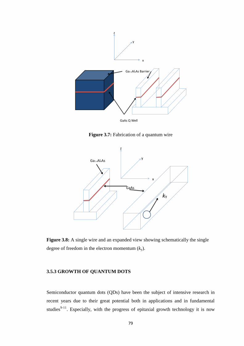
79
Figure 3.7: Fabrication of a quantum wire
Figure 3.8: A single wire and an expanded view showing schematically the single
degree of freedom in the electron momentum (ky).
3.5.3 GROWTH OF QUANTUM DOTS
Semiconductor quantum dots (QDs) have been the subject of intensive research in
recent years due to their great potential both in applications and in fundamental
studies9-11
. Especially, with the progress of epitaxial growth technology it is now
GaAs Q Well
Ga1-xAlxAs Barrier
x
y
z
ky
GaAs
x
y
z
Ga1-xAlxAs

80
possible to precisely control the quantum dots in term of size, composition and
density in order to achieve desired electrical and optical properties. On the
applications side, quantum dots could be the best candidate for the next generation of
photonics devices, such as high performance lasers and photo-detectors.
Semiconductor quantum dots have unique discrete states due to the three
dimensional confinement. In principle, quantum dot lasers can achieve high
efficiency because nearly all of the energy is concentrated in the ground state and
they can have excellent temperature stability due to the discrete energy levels.
Quantum dot detectors can cover a very broad range of wavelengths because of the
various discrete energy states in the QDs based on their inter-band and inter-subband
transitions. In fundamental studies, quantum dots can be regarded as artificial atoms
because they have discrete energy states like atoms or molecules; so it is possible to
make quantum dots with various structures to study various quantum effects or
discover new phenomena.
Quite a few methods for the fabrication of QDs have been used over the last twenty
years including lithography-based technologies. This technique, which is widely
used to fabricate QDs, predominantly by the combination of high-resolution electron
beam lithography and etching lithographic methods and subsequent processing, has
some drawbacks as highlighted below:
1. Size limitation prevents the observation of strong quantization effects
2. Formation of defects due etching
3. Size non-uniformity
4. Poor interface quality
5. Damage to the bulk crystal
A new attractive method of defect free 10 nm scale QD fabrication is the Stranski-
Krastanov (SK) growth in lattice-mismatched systems. This can occur when a thin
layer of a semiconductor is grown on a substrate whose lattice constant differs from
that of the epilayer. In the SK growth mode the mismatched epitaxy is initially
accommodated by biaxial compression in a layer-by-layer (2D) growth region,
traditionally called the wetting layer. After deposition of a few monolayers the strain
energy increases and the development of islands (0D) becomes more favourable than
planar growth.

81
For a system in which this occurs the transition between coherently strained 2D
growth and the onset of 0D island growth is reached after a 'critical thickness' (dc) of
epitaxial material has been deposited. The critical thickness is defined as:
| |
3.10
Where as is the lattice constant of the substrate material and ε is the strain between
the two materials. ε is defined as:
3.11
Where al is the lattice constant of the epilayer
This critical thickness decreases by increasing the lattice mismatch (as - al) between
the epitaxial material and the substrate. The transition from a purely 2D to 3D
growth during the deposition of a strained epitaxial layer is referred to as the Stranski
- Krastanow growth mode. Figure 3.9 shows SK growth mode of self-assembled
quantum dots. In the first two stages (Figure 3.9. a,b), a strained but uniform layer of
InAs grows with the same lattice parameter as that of GaAs substrate. This forms
what is called wetting layer which is a narrow quantum well. Beyond a certain layer
thickness called critical thickness, strain makes it energetically favourable for the
InAs to form small three-dimensional islands (Figure 3.9.c), which constitute the
self-assembled quantum dots. Growing more materials after that may lead to
dislocations (Figure 3.9.d). To obtain a good optical efficiency from grown quantum
dots, a capping layer (usually the same material as the substrate) is deposited over
the dots. This protects the dots and avoids problems with surface recombination
effects.
For InAs/GaAs QDs, SK growth occurs after as little as 1.7 monolayers (MLs) of
InAs has been deposited. The critical thickness (dc) increases with decreasing Indium
(In) fraction, reaching ~4 MLs for In0.5.Ga0.5As/GaAs QDs. The lowest In
composition that can support islanding of the InxGal-xAs layer appears to be ~25%.

82
One of the advantages of SK growth of QDs, an in-situ technique, is that no
processing is required. Since the dots are grown in-situ, a homogeneous surface
morphology is maintained and defect creation is avoided. However, the inherent
problem associated with this method is the size non-uniformity (~10%) and the
position uncontrollability of the QDs. Controlling the dimension and arrangement of
the self-organized 0D structures is thought to be very important for obtaining good
properties of the structures.
By adjusting the growth parameters such as deposition rates and temperature, the
composition, size, shape and surface density of the dots can be controlled. Post-
growth annealing provides an additional control parameter. The fabrication of self-
assembled quantum dots (SAQDs) by the SK method has been applied to numerous
combinations of semiconductor materials, including III-V semiconductor compounds
(InxGa1-xAs/GaAs, InxGa1-xAs/AlGaAs, and InP/GaInP), II-VI materials
(CdSe/ZnSe), and wide band gap nitrides (GaN/AlGaN).
Figure 3.9: Stranski-Krastanow growth mode of self-assembled quantum dots. (a)-
(d) show sequential stages in the growth of InAs quantum dots on a GaAs substrate.
(a) shows the substrate only; (b) InAs is deposited on the substrate: a thin, uniform
layer grows, forming a narrow quantum well called the wetting layer; (c) beyond a
certain layer thickness, the strain due to the lattice constant mismatch between the
materials causes small islands of InAs to form; (d) a GaAs capping layer is grown
over the dots for optical characterisation.

83
3.6 CARRIER DYNAMICS IN LOW DIMENSIONAL SEMICONDUCTOR
STRUCTURES
Due to the hetero-interface of two materials and the discrete nature of the quantum
dot levels, carrier dynamics in QD structures are considerably more complex than in
bulk materials. Figure 3.10 depicts a simplified band diagram of a semiconductor
QD structure under excitation with light, as found for instance in photoluminescence
experiments. Here, the excitation is assumed to occur in the barrier, i.e. the material
surrounding the QDs, for example GaAs in the InAs/GaAs system. The wetting layer
(WL), on which the QDs form in self-assembled growth, acts as an additional QW in
the structure. The dynamic carrier processes thus include:
1. Excitation of electrons from the barrier valence band into the conduction
band, thereby creating free electrons in the conduction band and free holes in
the valence band.
2. Relaxation from the barrier to the wetting layer.
3. Capture of the carriers into the quantum dots. The capture can occur either
to the ground state or to higher energy states with subsequent relaxation.
Capture directly from barrier states is also possible.
4. Carrier relaxation via carrier-carrier interaction (Auger effect) or carrier
phonon interaction.
5. Carrier transfer from the QD to nearby deep level traps leading to carrier
trapping and/or nonradiative recombination.
6. Radiative recombination where an electron and hole annihilate each other.
The energy released in the process is emitted via creation of a photon. Other
possible processes are radiative and nonradiative recombination of carriers in
WL and barrier conduction/valence band and thermal escape of the electrons
and holes from the quantum dots.

84
Figure 3.10: simplified band diagram of a semiconductor QD structure under
excitation with light showing the different processes as explained above.
Higher-energy transitions in a nanostructure can be observed in emission if a
powerful excitation source is used. The density of electrons and holes is sufficiently
large that the underlying electron and hole states are populated. The lower energy
states become fully occupied and carriers are prohibited from relaxing into these
states by the Pauli Exclusion Principle.
Radiative recombination
Photoluminescence
Carrier trapping
nonradiative recombination
6
5
4
1
2
3
Excitation
CB WL
VB

85
REFERENCES
1 A. Fox, Contemporary Physics, 37, 111 (1996).
2 D. Miller, D. Chemla, D. Eilenberger, P. Smith, A. Gossard, and W. Tsang,
Applied Physics Letters, 41, 679 (1982).
3 D. Mowbray, chapter 3, Nanoscale Science and Technology, book, Edited by R. W.
Kelsall, The University of Leeds, UK John Wiley & Sons Ltd (2005).
4 M. J. Steer, D. J. Mowbray, W. R. Tribe, M. S. Skolnick, M. D. Sturge, M.
Hopkinson, A. G. Cullis, C. R. Whitehouse, and R. Murray, Physical Review B, 54,
17738 (1996).
5 M. A. Herman, and H. Sitter, Molecular Beam Epitaxy, Springer-Verlag, Berlin,
(1996).
6 P. Blood, Semiconductor physics / quantum wells and GaAs-based structures,
Encyclopedia of Modern Optics, 9 (2005).
7J. Wang, D. A. Thompson, B. J. Robinson, and J. G. Simmons, Journal of Crystal
Growth, Volumes, 175–Part 2, 793 (1997).
8 S. Kim, J. Ro, K. Park, and E. Lee, Journal of Crystal Growth, 201 , 828 (1999).
9 L. Jacak, P. Hawrylak, and A. Wojs, Quantum dots. Berlin: Springer Verlag,
(1998).
10 D. Bimberg, M. Grundmann, and N. N. Ledentsov, Quantum Dot
Heterostructures. New York, John Wiley & Son Ltd, (1999).
11 D. G. Deppe, H. Huang, and O. B. Shchekin, IEEE Journal of Quantum
Electronics, 38, 1587, (2002).

86
CHAPTER 4: EXPERIMENTAL TECHNIQUES

87
This chapter describes the optical Photoluminescence (PL) spectroscopy,
transmission electron microscopy )TEM) and secondary ion mass spectroscopy
(SIMS) characterization techniques used to investigate the semiconductor samples
presented in this thesis. The hardware and software required to implement these
methods are also presented. The sample growth and annealing conditions are
described in the relevant chapters
4.1 PHOTOLUMINESCENCE
Photoluminescence (PL) is the spontaneous emission of light from a material under
optical excitation. The term “luminescence” (the literal translation from Latin is
“weak glow”) was introduced into the literature by Wiedemann in1888. Prefix photo
refer to this luminescence initiated by photoexcitation. There are several types of
luminescence depending on the cause or duration. Excitation by absorbance of a
photon leads to a major class of technically important luminescent species which
fluoresce or phosphoresce. In general, fluorescence is “fast” (ns time scale) while
phosphorescence is “slow” (longer time scale, up to hours or even days).
Photoluminescence (PL) provides information about the size and quality of
semiconductor structures containing quantum wells, wires or dots. In a PL
experiment light of sufficient energy greater than the bandgap of investigated sample
is incident on a material; photons are absorbed followed by electron hole pair
creation. Once the electrons and holes have relaxed to their band edges excitons may
form. Recombination of the carriers now occurs via either radiative or non-radiative
processes. If radiative relaxation occurs, the emitted light is called PL.
Fig. 4.1 (a) shows the photo-excitation of an electron from the valence into the
conduction band and intra band relaxation to band edge Fig. 4.1 (b) and finally the
electron–hole recombination and photon production are illustrated in Fig. 4.1 (c).
The emitted light can be collected and analyzed to yield a wealth of information
about the photoexcited material. PL investigations can be used to characterize a
variety of material parameters. The PL spectrum provides the transition energies,
which can be used to determine electronic energy levels. The PL intensity gives a
measure of the relative rates of radiative and nonradiative recombination. The

88
intensity and full width at half maxmuim (FWHM) of the PL signal as well provides
information on the quality of sample.
PL is simple, versatile, and nondestructive. Indeed, the technique requires very little
sample preparation or environmental control. Because the sample is excited
optically, there is no need for electrical contacts or junctions and high-resistivity
materials cause no practical difficulty. This feature makes PL mostly attractive for
samples having higher resistivity or undeveloped contact/junction technology.
Another advantage of the PL is that the luminescence can be investigated at different
regions on the sample surface.
The main disadvantage of PL analysis originates from its reliance on optical
techniques: the sample under investigation must emit photons. Indirect-bandgap
semiconductors, where the conduction band minimum and the valence band
maximum don’t have the same value in momentum space, have inherently low PL
efficiency. Nonradiative recombination tends to dominate the relaxation of excited
populations in these materials. Another shortcoming of PL is the difficulty in
estimating the density of traps and impurity states. When these states have radiative
levels, they are readily identified in the PL spectrum, and the intensity of the
associated PL peaks provides a relative measure of their presence in the sample.
However, measuring the absolute density of these state is different1.
Figure 4.1: Schematic illustration of the basic processes involved in luminescence
emission from optically excited semiconductors.
Conduction Band
Valence Band
b ) Intraband Relaxation
Conduction Band
Valence Band
a ) Excitation of an electron
from V.B to C.B
h
c) e-h recombination
and photons emission
PLE
Valence Band
Conduction Band

89
4.1.1 SYSTEM HARDWARE IMPLEMENTATION
This section describes the hardware required to implement a PL system which is
interfaced with a computer. The PL system is capable to operate over the temperature
range 10K-350K.
The block diagram and photograph of the PL system used in this work is shown in
Figures 4.2 and 4.3, respectively. Some of the important elements of the PL system
are described below.
4.1.1.1 SPECTROMETER
To allow spectral analysis, the emitted photoluminescence was dispersed using a
grating spectrometer. The iHR 550 spectrometer used in this study was purchased
from Horiba Jobin Yvon. It has a focal length of 0.55 m and aperture of f/6.4. It
offers a motorized grating turret which has the capacity to hold three different
gratings. Gratings with the following specifications are used: 1200 grooves/mm
blazed at 500 nm, 600 grooves/mm blazed at 2000 nm and 300 grooves/mm blazed at
3000 nm. The entry and exit slits are adjustable from 0.1mm to 2mm. The
spectrometer is capable of scanning with a speed of 160 nm/sec. The iHR 550 allows
minimum step size of 0.025nm. It also offers a motorized internal filter wheel with
capacity to accommodate six different filters which are placed just after the entry slit
inside the spectrometer. The iHR550 has two entrance and two exit ports available.
One exit port is configured for use with a photomultiplier tube detector (PMT), and
the other one configured with a Si/InGaAs dual detector.
4.1.1.2 LASERS, LIGHT CHOPPER AND OPTICS
The PL setup is equipped with excitation sources consisting of blue, green and red
lasers. The power of the laser incident on the sample can be tuned manually by using
a natural density filter. A mechanical light chopper is utilised to chop the laser light.
A band-pass filter is implemented in the path of the laser light to stop the unwanted
higher order lines of the laser light. Optics including lenses and reflectors are
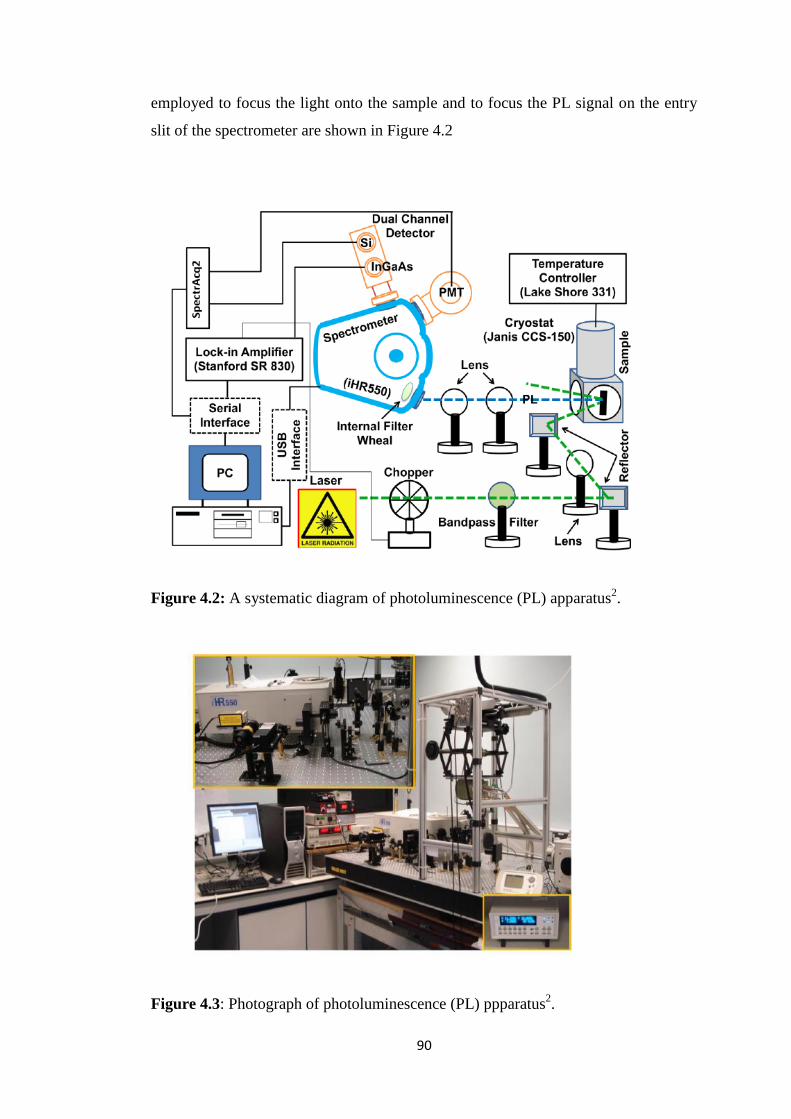
90
employed to focus the light onto the sample and to focus the PL signal on the entry
slit of the spectrometer are shown in Figure 4.2
Figure 4.2: A systematic diagram of photoluminescence (PL) apparatus2.
Figure 4.3: Photograph of photoluminescence (PL) ppparatus2.

91
4.1.1.3 DETECTORS
Optical detectors are opto-electronic devices used to convert incident photons to
electronic signals; the spectrometer is equipped with two detectors. One dual channel
solid state detector Si/InGaAs from Horiba Jobin Yvon is attached at the side exit of
the spectrometer. It can cover the optical range from 300 nm to 1700 nm. The silicon
operates up to 1.1 µm above which it becomes transparent and the InGaAs detector
operates from ~1.1 µm up to 1.7 µm . A single channel photomultiplier tube (PMT)
is placed at the front exit of the spectrometer. PMT detectors typically offer much
higher sensitivity than solid state detectors and operate effectively in the UV/VIS and
NIR. However, typically their spectral coverage is limited to about 950 nm. PMT
detectors also require high voltage power supplies. It can detect the light in the
spectral range from 180nm to 900nm.
4.1.1.4 SPECTRACQ2
To process and amplify the collected signals from the detectors, data acquisition
units are commonly used. SpectrAcq2 is a data acquisition module from Horiba
Jobin Yvon. It is a high speed unit that has the capability to capture and process 1000
data points per second collected from PMT or from Si/InGaAs detectors, and store
data of up to 5000 data points. SpectrAcq2 is Configurable for current or voltage
signal inputs. This module provides an analog high voltage output for controlling
PMT (~ 950 Volts). Communication between the computer and SpectrAcq2 is via a
serial port RS-232.
4.1.1.5 LOCK-IN AMPLIFIER
Lock-in amplifiers (LIA) are usually employed when very small AC signals need to
be detected and any other unwanted signals have to be rectified. The LIA
measurement is based on the phase sensitive detection, which basically refers to the
demodulation or rectification of the noisy signal from the detector by mixing with a

92
reference signal coming from the mechanical chopper that is used to chop the light
with fixed frequency.
The lock-in amplifier is fed by two signals; one is a control signal from a detector
connected to the chopper, and the other is a response signal from the monitoring
device. The purpose of the lock-in amplifier is then to selectively amplify only
components of the response signal which oscillate at the same frequency as the
control signal. The result is a very effective discrimination of noise, and hence a
large increase in the signal to noise ratio is obtained
A digital lock-in amplifier, model Stanford SR830 DSP has been implemented in the
PL setup. SR830 has the capability to measure and amplify very small signals down
to few nano-volts (nV) with sensitivity of 2 nV.
4.1.1.6 CRYOSTAT AND TEMPERATURE CONTROLLER
For the temperature dependent PL measurements a state-of-the-art cryostat, model
Janis CCS-150 has been used. To control the temperature of the sample, a
temperature controller, model Lake Shore 331, along with cryostat have been
implemented for our low temperature PL setup. It also consists of a cold finger,
radiation shield, homemade sample holder, aluminium vacuum shroud and thermal
sensors. The principle of refrigeration is based on close-cycle flow of helium gas
(He) through a compressor. It allows scanning the temperature from 10K to 350K.
4.1.1.7 COMPUTER INTERFACE
A computer with 120MB RAM, 200MB hard disk, windows XP as an operating
system, a high speed USB port, a serial port RS-232 is the minimum requirement for
the PL apparatus interface. The spectrometer is interfaced with computer via USB
port. Data acquisition box spectrAcq2 and lock-in amplifier are connected to the
computer by means of serial port RS-232 and can be initialized and controlled from
computer. A filter wheel fitted inside the spectrometer can also be controlled through
high speed USB port2.

93
4.1.1.8 SYSTEM CONTROLLING SOFTWARE
Software, named SynerJY, which has been supplied by Horiba Jobin Yvon is used to
control each equipment of the PL system remotely. The software facilitates the
selection of suitable grating, detector and entry/exit slit widths etc. Different
parameters which are required to perform the PL measurement can be entered
through software. The software is flexible in terms of recording and processing data
simultaneously. The software can drive the turret containing three gratings, slits, and
shutters. It also has control over the entrance and exit mirrors to select detector at
axial and side positions. A filter wheel having different colour filters situated inside
the spectrometer can also be controlled using the software.
4.2 STRUCTURAL CHARACTERIZATION
Structural characterization of the samples was made using a transmission electron
microscopy (TEM) technique to build up a full picture of the epitaxial layers. A
visual image of the quantum wells was achieved with TEM. Elemental analysis was
carried out using energy dispersive X-ray (EDX) technique.
4.2.1 ELECTRON MICROSCOPY
Transmission electron microscopy (TEM) is perhaps the most powerful analytical
tool available to material analysis. TEM can yield information about the topography
(surface features of an object), morphology (shape and size of the particles making
up the object), composition (the elements and compounds that the object is composed
of and the relative composition) and crystallographic information (how the atoms are
arranged in the material).TEM operates by exciting highly energetic electrons from a
source, where the electrons are focused and collimated along the optic axis of the
microscope and passed through a thin specimen (normally less than 1 μm). The
transmitted electrons are then used to form an image, diffraction pattern, or chemical
spectrum of the specimen.
The basic components in all electron microscopes (EMs) are the following:

94
1- Electron gun producing a stream of electrons in high vacuum. This stream is
accelerated towards the specimen (with a positive electrical potential).
2- Metal apertures and magnetic lenses to confine and focus electron beam into
a thin, focused, monochromatic beam.
3- the imaging system
When an accelerated beam of electrons impinges upon a sample a rich variety of
interactions takes place (see Figure 4.4). The versatility of electron microscopy and
X-ray micro analysis is derived in large measure from this variety of interactions that
the electrons undergo in the specimen. The interactions that occur during the
collision of the electron beam and the sample include directly transmitted electrons,
backscattered electrons, secondary electrons, coherent elastic scattered electrons,
incoherent inelastic electrons, incoherent elastic forward scattered electrons,
characteristic x-rays, and Auger electrons. In principle all these products of primary
beam interaction can be used to derive information on the nature of the specimen.
TEM produces images by detecting electrons that are transmitted through the sample,
while the Scanning Electron Microscope (SEM) produces images by detecting
secondary electrons which are emitted from the surface due to excitation by the
primary electron beam. Generally, TEM resolution is about an order of magnitude
better than SEM resolution.
Energy Dispersive X-ray (EDX) spectrometry makes use of the X-ray spectrum
emitted by a solid sample bombarded with electrons to obtain a chemical analysis.

95
Figure 4.4: Effects produced by electron bombardment of a material
4.2.2 TEM INSTRUMENTATION
TEM and EDX measurements were carried out at LPN, CNRS, France by Dr G.
Patriarche, and Dr D. Troadec.
TEM was performed on a 200 kV Jeol2200FS microscope with a spherical aberration
corrector on the scanning transmission electron microscope (STEM) probe. The
STEM-HAADF (high-angle annular dark- field) images are detected with a half
angle of 100 mrad (inner detector angle) and170 mrad (outer angle). The corrected
convergence half angle of the STEM probe is 30 mrad and the probe intensity is 55
pA. The acquisition time is 38.7 s per image (1024×1024 pixels).
Incident Electrons Beam
Secondary electrons
Characteristic X-ray
Backscattered electrons
Auger Electrons
Inelastically Scattered Electrons
Transmitted Electrons
Elastically Scattered Electrons

96
4.3 TIME OF FLIGHT SECONDARY ION MASS
SPECTROMETRY
4.3.1 INTRODUCTION TO SECONDARY ION MASS SPECTROMETRY
(SIMS)
Secondary ion mass spectrometry (SIMS) is an ultra-high vacuum (UHV) technique
that measures the ionized particles that are released when a surface is bombarded
with an energetic primary particle. Primary ion sources commonly used in SIMS
include cesium, gallium and bismuth3.
The secondary particles are emitted from the surface after bombardment from the
primary ions as the ion beam is pulsed for short periods. The energy is transferred
from primary ions to the surface which allows surface atoms and molecules of
approximately the top 2-3 molecular layers to overcome their surface binding
energy4,5
(i. e. the top 2 nm of sample). Emitted particles can take the form of
electrons, neutral atoms or molecular species, cluster and atomic ions. The
production of secondary ions from a surface is represented schematically in Figure
4.5.
Figure 4.5: Diagram illustrating the production of secondary ions from a surface.
2 nm
Primary Ion
Beam - - -
-
-
- -
+
+
+
+
+
+
+
Mass
Spectrometer
Secondary Ions
Sample Surface

97
Secondary ion emission by a solid surface under ion bombardment supplies
information about the elemental, isotopic and molecular composition of its
uppermost atomic layers. The secondary ion yields will vary greatly according to the
chemical environment and the sputtering conditions (ion, energy, and angle). These
results in a mass spectrum that characterizes the chemical composition of the sample
under investigation, The spectra produced can be used to provide detailed
information on the spatial distribution of components, structure6 and orientation
7 of
chemistries at the surface8.
4.3.2 THEORY OF TOF-SIMS OPERATION
A time-of-flight instrument allows much greater mass resolution to be obtained than
older systems which employ quadrupole detectors. Secondary emitted ions are
accelerated over a very short distance resulting in all the ions having almost the same
kinetic energies, which is vital to the working of the time-of-flight spectrometer. The
energy and angular dispersion of the secondary ions can be compensated using
focusing elements such as a reflectron resulting in improved mass spectrum9.
Secondary emitted ions can have a spread of energies, and this will lead to low mass
resolution analysis. Ions with diverse energies will penetrate the reflectron to
different depths, i.e. the higher the energy of the ion, the deeper the penetration
before it travels further towards the detector. This additional step before detection
lead to compensation of the difference in energy spread10
.
The ionised species then travel through a flight tube on their way to the mass
analyzer. A fixed voltage accelerates the secondary ions into the ToF analyzer, with
its polarity determining whether positive or negative secondary ions are analyzed.
The ions are separated by mass, and as the lower mass ions have a higher velocity
they will reach the detector faster than heavier ions. The flight tube has a known path
length (L). The time (t) taken for each ion to arrive at the detector at the end of tube
can be measured11
. A simple equation can be used to produce a ToF-SIMS spectrum
and thus derive the mass of the ions.
The ion velocity, v, is the length of the flight path, L, divided by the flight time, t

98
vL
t
4.1
Substituting this expression for v into the kinetic energy relation, one can derive the
working equation for the time-of-flight mass spectrometer:
( )2
mt L
zv
4.2
Technological advances in computing have allowed the whole mass spectrum to be
collected in parallel. The mass spectra consist of the ion mass charge ratio versus the
number of ions detected. ToF mass analysers are currently the most widely used type
of analyser for SIMS and have been employed in all work shown in this thesis.
4.3.3 MODES OF ANALYSIS USING TOF-SIMS
There are three basic modes of SIMS operation:
Point Analysis: a focused stationary beam is used to determine the composition
at a certain point. The target size is usually between 1 and 25 µm but is
dependent on the application.
Imaging: rastering the primary ion beam to obtain compositional images of the
surface. SIMS images with a spatial resolution of better than 50 nm are
obtainable.
Depth profiling: scanning a sputter ion source over the surface of the sample
causes the surface layers to be slowly eroded, revealing the compositional
change with depth.
The aim of depth profiling is to obtain information on the variation of composition
with depth below the initial surface. This is useful for the analysis of layered
structures and has been employed to investigate samples discussed in this thesis.

99
The depth profile is obtained using two separate beams mounted at 1800 to one
another where one beam is used to progressively etch a crater in the surface of the
sample under study, whilst short-pulses of a second beam are used to analyze the
centre of the crater. This has the advantage that one can be confident that the analysis
is exclusively from the base of the etch crater and not affected by sputtering from the
crater-walls. Depth profiling is undertaken in dynamic SIMS (DSIMS) mode (dose
of primary ion larger than static limit (> 1×10¹³
ions/cm2).
4.3.4 TOF-SIMS INSTRUMENTATION12
SIMS measurements have been performed at the School of Pharmacy, Nottingham
University by Dr David Scurr.
A ToF-SIMS IV (ION-TOF, Münster, Germany) fitted with Cs+ column was used
for all SIMS data shown in this thesis. An automated electronic stage control module
was used to move the stage within the main chamber. The pressure was maintained
below 6 × 10⁻⁸
Torr for analysis but within the initial load lock a pressure of 1 × 10⁻⁶
was sufficient to move the sample stage from the load lock to the main chamber (see
Figure 4.6). When loading the sample stage into the ToF-SIMS, anti-static gloves
were used in order to reduce the opportunity for any static charge to influence
electronics within the main chamber.

100
Figure 4.6: Schematic of the ToF-SIMS machine and typical set up of IonTOF ToF-
SIMS IV instrument.
Ion Gun
Pulsing
Focusing
Raster
Target
Ion Mirror
Spectrum
Detector
Extractor

101
REFERENCES
1 T. H. Gfroerer, Encyclopedia of Analytical Chemistry R.A. Meyers (Ed.), John
Wiley & Sons Ltd, Chichester, 9209 (2000).
2 M. Shafi, Electrical And Optical Studies Of Dilute Nitride And Bismide Compound
Semiconductors, PhD Thesis, Nottingham University (2011).
3 J. Vickerman, and D. Briggs, ToF-SIMS: Surface Analysis by Mass Spectroscopy,
Manchester: IM Publications and Surface Spectra Limited (2001).
4 R. La, and S. A. John, American Journal of Physiology, 266, 1(1994).
5 J. C. Vickerman, and D. Briggs. TOF-SIMS: Surface analysis by mass
spectrometry, Chichester: IM Publications (2001).
6 M. S. Wagner, and D.G. Castner, Langmuir, 17(15), 4649 (2001).
7 P. Bertrand, Applied Surface Science, 252(19), 6986 (2006).
8A. M. Belu, D. J. Graham, and D. G. Castner, Biomaterials, 24(21), 3635 (2003).
9A. M. Belu, D. J. Graham, and D.G. Castner, Biomaterials, 24(21), 3635 (2003).
10 D. Briggs, Surface Analysis of Polymers by XPS and Static SIMS. Cambridge:
Cambridge University Press, (1998).
11J. C. Vickerman, and I.S. Gilmore, Surface Analysis: The Principal Techniques,
Vol 2, John Wiley & Sons Ltd. (2009).
12 A. rafati, PhD Thesis, The Analysis of Polymers For Biomedical Applications,
Nottingham University (2011).

102
CHAPTER 5: OPTICAL PROPERTIES OF SELF-
ASSEMBLED InAlAs/AlGaAs QDs GROWN BY MBE ON
DIFFERENT GaAs SUBSTRATE ORIENTATIONS

103
In this Chapter, optical characterization technique, namely photoluminescence (PL)
has been employed to study the effect of GaAs substrate orientation [i.e, (100),
(311)A, (311)B)] on the optical properties of InAlAs/GaAlAs/GaAs Quantum Dots
(QDs). Optical properties of InAlAs/GaAlAs QDs formed under different growth
conditions (growth temperature, different confinement barriers, and amount of
deposited material) have been studied.
5.1 INTRODUCTION
During the last years, the fabrication of self-assembled quantum dots (SAQDs) by
Stranski Krastanow (SK) growth mode1 has attracted much attention both for basic
physics and optoelectronic device applications. SAQDs that emit in the infrared
region, have been successfully fabricated with many different material combinations
including In(Ga)As/GaAs2,3
, GaSb/GaAs4, InP/InGaP
5 and In(Ga,Al)As/InP
6-8.
However, there are only few reports on the use of SAQDs that emit in the red part of
the visible spectrum. These are based on AlInAs/AIGaAs material system that has a
larger band gap9 than for example InAs/GaAs system.
InAlAs/AlGaAs QDs exhibit a shorter photoluminescence (PL) peak wavelength,
typically, around 700 nm (1.77 eV) at 10 K, whereas the typical peak is around 1070
nm (1.158 eV) for InAs/GaAs QDs10
. In addition, the PL spectra have a relatively
narrow line width, typically, 50–60 meV. Visible emissions with narrow line width
are important in many applications, including high density optical storage.
W. Zhou et al11
investigated 10 MLs self-organized In0.55Al0.45As QDs on
Al0.5Ga0.5As matrix deposited on (100) GaAs substrates by MBE. The AlGaAs
matrix and the InAlAs QDs were grown at a temperature of 700 0C and 600
0C,
respectively. A bimodal distribution of quantum dot sizes has been demonstrated by
atomic force microscopy (AFM). There are two predominant families of the lateral
dot sizes. Their average sizes were about 26±5nm and 53±7nm, and their densities
were about 5.9 x10¹⁰
cm–2
and 1.5x10¹⁰
cm–2
, respectively. The optical properties of
lateral size bimodal distribution of these QDs were studied, and by taking into
account quantum-size effect on the peak energy, they proposed that the high (low)
energy peak results from a smaller (larger) dot family. The PL emission energies

104
from the small and large QDs were found to be ~ 1.941 eV (~640 nm) and, ~1.85 eV
(~670nm) respectively.
X. Lu et al12
studied the effects of growth conditions on the size and density of self-
assembled InAlAs/AlGaAs QDs grown on GaAs by MBE. Their aim was to achieve
low density QDs, which is relevant for investigations of single QD spectroscopy. It
has been observed that the diameter increases and the density decreases with
increasing substrate temperature or with decreasing growth rate. They obtained a dot
density as low as 1x10¹⁰
cm-2
for optimized growth conditions.
S. Fafard et al13
carried out a systematic study on the optical and structural properties
of MBE grown InxAl(1-x)As/AlyGa(1-y)As QDs with various In and Al compositions
by using low-temperature PL and transmission electron microscopy (TEM). All
these QDs emitted in the visible range. The major aims of their study was to
determine (i) the dependence of the 2D to 3D transition on the interfacial energy by
varying the amount of Al in the AlyGa1-yAs cladding layers surrounding InAlAs
QDs, and (ii) the critical thickness for the formation of InxAl1-xAs surrounded by
AlyGa(1-y)As cladding layers. It was found that (i) the number of monolayers
deposited until the 2D/3D transition occurs does not depend on the Al content of the
cladding layers; (ii) the critical thickness increases as the Al content in the QD
increases.
A. Tsatsulnikov et al14
studied structural and optical properties of InxAl1- xAs QDs
embedded in an A10.3Ga0.7As matrix as a function of InAs mole fraction (x). A
decrease in indium composition to values less than ~ 0.43 resulted in a gradual
disappearance of bound electron states in QDs. In this case, the PL emission is
governed by a type-II optical transition between electrons localized in the
A10.3Ga0.7As layer and holes localized in the QDs. Reflection high-energy electron
diffraction (RHEED) showed that QD formation started after depositing ~ 9 Å and ~
14 Å InA1As for In =54% and 43%, respectively. By decreasing the In material
content to a value ~34%, no dots are formed even with increasing the deposition
material to 22 Å. In0.54Al0.46As QDs have a peak PL emission at 1.6 eV with Full
Width at Half Maximum (FWHM) of ~100 meV. By decreasing the In content by
~10 percentage, a shift in PL maximum towards higher photon energies (~100 meV)
occurred. The QDs have a lateral size of about ~ 180Å and height of ~ 30 Å.

105
H. Liu et al15
have employed AFM, PL, and EL (electroluminescence) to study the
effect of the growth temperature on the optical and structural properties of 5MLs
In0.65Al0.35As/Al0.35Ga0.65As QDs. The best optical and structural quality of the
In0.65Al0.35As/Al0.35Ga0.65As QDs has been demonstrated at the growth temperature
of 560 °C. Furthermore, under continuous wave conditions the QD laser diodes with
the In0.65Al0.35As/Al0.35Ga0.65As QD active layer grown at 560 °C emit at an energy
of 1.651 eV with a threshold current density of 410 A/cm2 at 220 K. This threshold
current is much lower than that of the InAlAs/AlGaAs QD laser with the active
region grown at 530 °C. The QD lateral size distribution obtained from AFM images
reveal an average island size of 27 nm in base width and an areal density of
~7.0x10¹⁰
/cm2 for the QDs grown at 530 °C. With increasing the growth temperature
to 560 °C, the density of the islands decreases to 5.3x10¹⁰
/cm2. Furthermore, the QD
size distribution becomes slightly narrower. The typical QD separation is estimated
by AFM to be 6.5 nm.
Theoretically, it is well established fact that the radiative lifetime in QDs is
independent of temperature due to the delta function of the density of states, which
leads to the limited thermal distribution as long as the energy separation is larger
than the thermal energy. However, B.L. Liu et al16
show the divergent results for
InAlAs/AlGaAs QD sample grown on (100)-oriented GaAs substrate. Using Time-
Resolved PL (TRPL), the constant decay time has not been observed even at low
temperature. Instead, the observed decay time increases quickly with increasing
temperature, showing 2D properties in the transient dynamic process. The measured
decay time increased from 1.47 ns at 12K to 3.6 ns at 30 K. They explain this longer
decay time at low temperature and this quickly increasing with temperature to the
lateral coupling in InAlAs/AlGaAs QDs due to their high density, which results in
the formation of the local minibands or extended states from the discrete energy
levels.
The surface morphology of self-assembled QDs is a key factor in determining their
optical properties, and it is very sensitive to the sample structure, such as the
composition of the buffer layer17
, surface reconstruction18
, and substrate orientation.
Up to date, most of the reported studies focused on the QDs grown on the
conventional (100) GaAs substrates. Recently, many high index polarized GaAs

106
surfaces, such as (311)A19
, (311)B20-24
, (411)A25
, and (411)B26
, have drawn greater
attention because these surfaces provide a natural structural corrugation27
. QDs
grown on theses surfaces have some unique properties, such as narrow size
distribution and high density. These enhanced properties can be used to further
improve the performance of devices.
QD formation on many high-index surfaces have been studied, and QDs formed on
some surfaces exhibit good structural and/or optical properties that are comparable
or superior to QDs on (100) surface.
S.Zhong-zhe et al28
studied ~13 MLs In0.9Al0.1As SAQDs formed by MBE on (100)
and (N11)B (N = 2, 3, 4, 5) InP substrates. QDs formation for all samples was
confirmed by TEM and PL. The PL spectra revealed striking differences in peak
position, line width, intensity and peak shape between different oriented surfaces.
QDs formed on (411)B surface gave the highest PL intensity, while QDs on (211)B
and (311)B orientations showed weaker PL emissions. These results show that QDs
emission can be improved by using non-conventional InP substrates. It is worth
pointing out that the trend of peak shift reported by S.Zhong-zhe is not similar to the
published results from InAs QD on high-index29
where blue shift is observed for
(N11)B surfaces, whereas red shift is observed for (N11)A orientations. This could
probably be attributed to the different material system or respective growth
conditions.
5.2 EXPERIMENTAL RESULTS AND ANALYSIS
The investigation of the optical properties of InAlAs QDs was carried in the
following sequence in order to determine the best GaAs substrate orientation and the
optimised growth conditions for the growth of these QDs:
1- Comparative study of the optical properties of Al0.35In0.65As QDs formed on
Al0.45Ga0.55As matrix and grown on different GaAs substrate orientations
[(100), (311)A and (311)B] at a growth temperature of 450 0C.
Two different Al0.35In0.65As coverage were investigated, namely 11 Å (3.7
MLs), and 13 Å (4.4 MLs).

107
2- Study of the effect of the AlyGa1-yAs matrix confining barrier (y= 0.25, 0.35,
0.45, and 0.55) on the optical properties of Al0.35In0.65As QDs grown on
(311)B plane at a temperature of 450 0C.
3- Study the effect of growth temperature (500 0C and 550
0C)on the optical
properties of (311)B Al0.35In0.65As QDs grown on Al0.45Ga0.55As matrix.
5.2.1 STUDY OF THE INFLUENCE OF THE SUBSTRATE ORIENTATION
ON THE OPTICAL PROPERTIES OF Al0.35In0.65As/Al0.45Ga0.55As QUANTUM
DOTS
This section will report on the optical properties of InAlAs QDs grown on the
conventional (100) and high index planes, namely (311)A and (311)B, GaAs
substrates. The aim is to determine the optimal substrate orientation for the growth of
these QDs on AlGaAs matrix.
All QD samples studied in this work have been grown by MBE on semi-insulating
GaAs substrates with orientations (100), (311)A and (311)B. All the growths were
carried out simultaneously and under the same conditions for comparison purposes.
The growth temperature, the growth rate and arsenic overpressure were 450 °C, 1μm
per hour, 1.2x10⁻⁵
Torr, respectively. The As:Ga beam equivalent pressure ratio as
measured by an ionization gauge was approximately 12:1. The samples were rotated
during growth in order to improve the uniformity of the layers. The layer structure is
shown in Figure 5.1.
The samples consisted of a 0.2µm-thick GaAs buffer layer of which the first 0.1 µm
was grown at 580 °C and the remaining 0.1 µm at 600 °C. The temperature was kept
at 600 0C during deposition of the Al0.45Ga0.55As matrix layer. This was followed by
the deposition of 11Å Al0.35In0.65As strained layer at 450 0C for the formation of 3.75
monolayers (MLs) QDs, a 50 nm Al0.45Ga0.55As cap layer, and 10nm GaAs. The
lattice constant mismatch between the InAlAs QDs and the AlGaAS matrix is ~
4.6%.
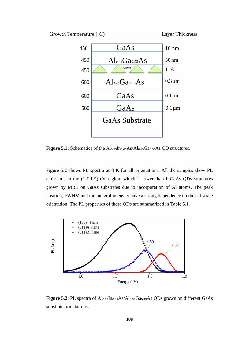
108
Figure 5.1: Schematics of the Al0.35In0.65As/Al0.45Ga0.55As QD structures.
Figure 5.2 shows PL spectra at 8 K for all orientations. All the samples show PL
emissions in the (1.7-1.9) eV region, which is lower than InGaAs QDs structures
grown by MBE on GaAs substrates due to incorporation of Al atoms. The peak
position, FWHM and the integral intensity have a strong dependence on the substrate
orientation. The PL properties of these QDs are summarized in Table 5.1.
Figure 5.2: PL spectra of Al0.35In0.65As/Al0.55Ga0.45As QDs grown on different GaAs
substrate orientations.
GaAs
0.1 µm
0.1 µm
GaAs
580
600
Al 0.45 Ga 0.55 As 600 0.3 µm
AlInAs
50 nm
450
450
11 Å
GaAs Substrate
Growth Temperature (0C) Layer Thickness
Al 0.45 Ga 0.55 As
GaAs 10 nm 450
1.6 1.7 1.8 1.9
x 50
PL
(a.u
)
Energy (eV)
(100) Plane
(311)A Plane
(311)B Plane
x 50

109
Table 5.1: PL peak energy (eV), FWHM (meV) and PL intensity ratios between
(100) QDs and high index QDs.
Plane PL Energy
(eV)
FWHM
(meV)
PL intensity /
PL intensity(100)
(100) 1.74 125 1.00E+00
(311)A 1.835 44 0.7E-02
(311)B 1.77 59 0.9E-02
A blue-shift in PL peak position is observed (see Figure 5.3) for QDs grown on
(311)A (1.835 eV) and (311)B (1.77 eV) with reference to (100) QDs (1.74 eV).
(311)A QDs have a higher emission energy than (311)B QDs. For the (311)
orientation the peak position depends upon whether the substrate is Ga terminated (A
face) or As terminated (B face).
This energy shift can be accounted by the effects the substrate orientation has on the
shape and average size of the overgrown QDs due to the different surface energy,
strain and growth kinetic24,29,30
. Generally speaking, QDs formed on high-index
surfaces are smaller in size than those on the (100) substrate, because on (N11)
surfaces, there is a high density of steps compared to the atomically flat (100)
surface. These steps will limit the in-plane diffusion of atoms during the growth, and
delay the formation of well-developed dots in terms of size with respect to the (100)
substrate31
.
However, it is not clear why (311)A QDs have a larger blue shift than (311)B QDs.
A possible explanation could be due to the slower diffusion of In and/or Al on the
Ga face than on the As face.
It is important to note that emission from the wetting layer was not detected in the
samples investigated in this work. The PL signature of the wetting layer is
sometimes not detected as reported by P. Gonzilez-Borrero et al32
for InGaAs QDs.
They interrupted the growth for 1, and 3 minutes before and after depositing the dots,
respectively. They explained the absence of the wetting layer emission due to driving
much of the deposited indium to the island nucleation. This process leaves a very
thin wetting layer, where carriers are generated and transferred very quickly (~ ps) to

110
the InGaAs QDs where they recombine radiatively. Similar explanation was given
by Z.Y. Xu33,34
for InAs/GaAs QDs.
S. Fafard et al35
attributed the absence of emission from wetting layer to the high
density of QDs. In their work they studied InAs/GaAs QDs grown on (100) GaAs
substrates, and reported that as the coverage increases, the amplitude of the wetting
layer PL peak decreases simultaneously with the increase of the QD PL peak
intensity. This was attributed to the increase of QDs density.
For the InAlAs QDs system, it was reported12
that the short surface diffusion of Al
due to its high bonding energy with As was responsible for the achievement of high
density of InAlAs QDs.
It is therefore concluded that the absence of the wetting letting PL signal in our
samples is related to the Al diffusion, which causes a high density of QDs.
As shown in Figure 5.4, the FWHM of QDs grown on high index planes is smaller
than those grown on (100) plane. The FWHM of (100), (311)B and (311)A QDs are
125 meV, 44 meV and 59 meV, respectively. J. He et al36
showed that the PL
FWHM drastically decreased as the uniformity of the QDs increased. It is well-
known that the smaller the FWHM the higher structural quality of QDs. This means
that (311)A QDs have a better size uniformity.
Figure 5.3: Effect of substrate orientation on the PL peak energy.
(100) (311B) (311A)
1.74
1.76
1.78
1.80
1.82
1.84
PL
En
erg
y (
eV
)
Growth Plane

111
Figure 5.4: Effect of substrate orientation on the PL FWHM.
Figure 5.5 gives the relative PL intensity of Al0.35In0.65As/Al0.45Ga0.55As QDs for
each sample. The PL intensity is normalized relative to that of (100) QDs.
Remarkably, the PL intensities for QDs on (311)B and (311)A surfaces are about
two order of magnitude less than for (100). This is in contrast to other type of QDs,
such as InAs and InGaAs37-39
formed on high index surfaces, which are characterized
by a stronger luminescence and a narrower linewidth than those grown on (100)
surface. It has been reported that the critical thickness for the formation of QDs on
high index plane is larger than for (100) plane40
. The lower luminescence of
(311)A/B QDs observed in this work may be due to the low amount of material
deposited (11Å) to achieve well-formed QDs. The critical thickness θc (the number
of monolayers of strained material necessary to induce the transition to island
growth) after the initial layer-by-layer growth at which the 2D (layer) to 3D (island
growth) transition occurs has been established to be strain dependent for InxGa1-xAs
on GaAs41,42
.
(100) (311)B (311)A
40
50
60
70
80
90
100
110
120
130
FW
HM
(m
eV
)
Growth plane

112
Figure 5.5: Relative integrated PL intensity of Al0.35In0.65As/Al0.45Ga0.55As QDs for
each sample. The integrated PL intensity is normalized relative to that of (100) QDs.
RHEED is generally used to determine the 2D/3D growth transition. Several
authors43,44
showed that the onset of the island nucleation for InAs QDs formation
starts well before the RHEED pattern changes from streaks to spots (~ 1.6 MLs).
S. Sanguinetti et al45
and Guryanov et al46
showed an increase of SK growth mode
onset as the growth substrate orientation departs from (100) towards (311) (see
Figure 5.6). Such behaviour can be understood in terms of strain relaxation
inhibition which takes place in low dimensional strained heterostructures grown on
(N11) substrates.
By means of equilibrium theoretical model which includes the substrate orientation
effects, S. Sanguinetti et al40
demonstrated that the delay of formation of dots as the
surface orientation departs from (100) towards (311) is a direct consequence of the
degree of strain relaxation in the island. The in-island elastic strain relaxation
becomes less efficient as the growth substrates departs from the (100) orientation.
Such inhibition of strain relaxation inside the islands, by increasing the island
internal energy term, should be the reason for the delay in the 3D growth mode onset
on (N11) substrates.
Contrary to what was expected, the (100) InAlAs QDs optical properties are better
than those of (311) QDs. The observed lower efficiency in our (311) InAlAs QDs
(100) (311B) (311A)
PL
In
ten
sity
(a
.u)
Growth Plane

113
could be explained by the theoretical work for the formation of QDs on high index
planes reported in Reference 40 .
Figure 5.6: 2D/3D growth transition critical coverage shift c
c
as a function of
the Miller index N for (N11) substrates ( c is the critical coverage). Empty squares
indicate the experimental points. Model predictions are indicated by black circles.
The line is a guide for the eyes40.
In order to obtain further information about the properties of QDs grown on different
planes, the temperature dependence of the PL spectra was also investigated. The
excitation energy was 2.62 eV (473 nm) and the excitation power was kept at 40
mW. The data is presented in Figure 5.7.
The results show that the PL intensity from dots grown on different substrates
quenches at different temperatures.
1N
0 0.1 0.2 0.3 0.4 0.5
c
c
1
1.1
1.2
1.3
(311)
(511)
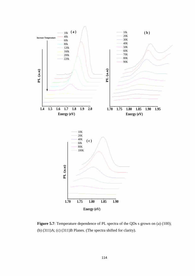
114
Figure 5.7: Temperature dependence of PL spectra of the QDs s grown on (a) (100);
(b) (311)A; (c) (311)B Planes. (The spectra shifted for clarity).
1.4 1.5 1.6 1.7 1.8 1.9 2.0
10k
40k
60k
80k
120k
160k
200k
220k
PL
(a.u
)
Energy (eV)
Increase Temperature
( a )
1.70 1.75 1.80 1.85 1.90 1.95
10k
20K
30K
40K
50K
60K
70K
80K
90K
PL
(a.u
)
Energy (eV)
( b )
1.70 1.75 1.80 1.85 1.90
10K
20K
40K
60k
80K
100K
PL
(a.u
)
Energy (eV)
( c )

115
Figure 5.8 illustrate the evolution of FWHM of the PL as a function of temperature
for the QD samples grown on (100), (311) A and (311) B substrates. A significant
difference can be seen for QDs grown on different substrates.
Figure 5.8: FWHM of PL spectra as a function of temperature for the QD samples
grown on different substrate orientations.
The FWHM increases monotonously with temperature for QDs grown on high index
planes. The FWHM increases from 44 and 59 meV at 10K for QDs grown on (311)A
and (311)B respectively to 105 and 103 meV at 100K.
The increase of the linewidth with temperature was reported before in the InAs QDs,
and attributed to electron phonon scattering47
. However, in the case of QDs grown
on (100) plane, an anomalous decrease of the linewidth with increasing temperature
was observed in the temperature range from 10 to 80 K, followed by normal increase
with the temperature.
This anomalous behavior of FWHM with temperature may be due to high dot
density formed on (100) plane, and which could favour thermally activated dot-dot
coupling channels. This can be explained as follows: at low temperatures, the PL line
shape of QDs is determined by the inhomogeneous distribution of QD sizes. That is,
PL arises from the sum of emission of many different dot sizes. When the
temperature increases, the thermalized carriers can relax to a nearby dot and find a
lower local-energy minimum, resulting in shrinkage of the linewidth34
. When the
temperature further increases (above 80K), the effect of electron-phonon scattering
becomes a dominant contribution. Consequently, the FWHM increases with
0 50 100 150 200 250
60
70
80
90
100
110
120
130
140
150
160
FW
HM
(m
ev
)
Temperature (K)
(100) Plane
(311)A Plane
(311)B Plane

116
temperature. These strange effects are not expected in an ideal QD structure in which
all the dots are largely separated and decoupled from each other.
Y. T. Dai et al48
studied this anomalous temperature dependent photoluminescence
(TDPL) for 3, 4, and 5MLs InAs/GaAs QDs. They reported that the turning
temperature (Tf) (the temperature of the minimal FWHM) strongly depends on the
dot sizes. Tf is higher for larger dot size. This behaviour can be explained by the fact
that the carriers in smaller dots have a higher ground state energy corresponding to a
lower binding energy. Thus, the carriers can be easily thermalized, which causes the
Tf of the smaller dot to appear at lower temperature.
The results of the temperature dependence of the PL peak position are shown in
Figure 5.9. The variation of the PL peak position with temperature of bulk
semiconductors can be attributed to the effect lattice stretching and electron-lattice
interaction. The fast red-shift of the PL peak with increasing temperature in QDs
system had previously been observed, and mainly had been attributed to the
redistribution of carriers among QDs with different sizes34,
49, 50
.
The red lines in Figure 5.9 are the experimental results, and the black curves are
fitting obtained by shifting the bulk InAlAs band gap along the energy axis, using
the empirical Varshni equation51
.
2
( ) (0)g g
TE T E
T
Where α (eV/K) is a constant, β is the Debye temperature, Eg(0) is the band-gap
energy at 0K, and T is the measured temperature. The constant values used for the
fitting shown in Figure 5.9 are based on Ref 53.
From Figure 5.9 (b), it can be seen that the peak energies of QDs grown on (311)A
show a redshift with increasing temperature with a rate basically identical to the bulk
material.
QDs grown on (100), and (311)B (Figure 5.9 a and c) show a faster red shift than the
Varshin’s relation of bulk InAlAs band gap. This unusual temperature dependence is
a characteristic of QDs which cannot be explained by the temperature-induced band-

117
gap change alone, because of the strong deviation from the Varshin’s relation of bulk
InAlAs band gap.
The (100) and (311) B QDs PL peak is red shifted by 64 meV and 46 meV,
respectively in the temperature region 10-100 K compared to 13 meV for the (311)A
QDs in the same region.
This fast red shift of (100) and (311)B QDs PL compared to (311)A QDs can be
explained by the larger inhomogeneous distribution and higher density of QDs on
(100) and (311)B substrates than on (311)A. This is also reflected in their PL
intensity and FWHM.
In the case of a multimodal distribution, at low temperatures, carriers are frozen
randomly into the different dot states of different size QDs, and the PL spectra reveal
the emission of the QD ensemble. With increasing temperature, carriers gain enough
energy to be activated outside the dot into the wetting layer and/or the AlGaAs
barrier and then relax into another dot. Carrier hopping between dots occurs by a
transfer of carriers from dots having lower binding energy towards the dots having a
higher binding energy. This results in a lower-energy emission with a narrow PL
spectra followed by a red shift of the luminescence peak that is larger than that
expected for the thermal shrinkage of the AlInAs band gap with increasing
temperature (i.e. due to the high density of QDs, coupling between QDs occur and
carriers transfer from the higher-energy to the lower-energy dot families resulting in
the fast red shift). Within a one size QDs family, the PL energy temperature
dependence normally follows the Varshni’s law for the temperature-dependent shift
of bulk energy gap.
Similar effects were observed by many groups. For example, H.Wang et al52
studied
two self-organized InAs/GaAs quantum dots grown by MBE on (100) oriented GaAs
substrates using PL and scanning tunnel microscopy (STM). The samples have
different dot densities of 1.9x10¹⁰
cm-2
and 3.0x10¹¹
cm-2
. It was reported that faster
red shift is observed in high density sample than lower density sample.

118
Figure 5.9: Temperature dependence of the PL peak energy for QDs samples grown
on different substrate orientations (a) (100), (b) (311)A, (c) (311)B. The black lines
are calculated according to the Varshni’s law using the parameters of bulk InAlAs
reported by D. Gaskill and co-workers53
and are shifted along the energy axis, and
(d) bulk InAlAs.
The optical quality of the InAlAs QDs on high index planes is found to be inferior to
that of (100) QDs. This could be due to the non-optimized growth conditions and
layer structure. It is worth pointing out that these samples were grown
simultaneously, and therefore the growth conditions might not be optimal for each
plane.
The following sections will report the effect of changing the growth conditions.
0 50 100 150 200 2501.60
1.65
1.70
1.75
En
erg
y (
eV
)
Temperature (K)
(100) Plane
InAlAs bulk (a)
0 20 40 60 80 1001.80
1.81
1.82
1.83
1.84
1.85
En
erg
y (
eV
)
Temperature (K)
(311)A Plane
InAlAs bulk (b)
0 50 100 150 2001.45
1.50
1.55
1.60
En
erg
y
(eV
)
Temperature (K)
InAlAs bulk
(d)
0 20 40 60 80 1001.72
1.74
1.76
1.78
1.80
En
erg
y (
eV
)
Temperature (K)
(311)B Plane
InAlAs bulk (c)

119
5.2.2 EFFECT OF INCREASING DEPOSITED InAlAs MATERIAL ON THE
OPTICAL PROPERTIES OF QUANTUM DOTS GROWN ON DIFFERENT
SUBSTRATE ORIENTATIONS.
The results reported in this section were obtained on Al0.35In0.65As/Al0.45Ga0.55As QD
samples which were grown under the same conditions and have the same layer
structure as those samples previously discussed except that the deposited
Al0.35In0.64As material is 13 Å instead of 11 Å (i.e, increasing from 3.7 MLs to 4.4
MLs).
Figure 5.10 shows low temperature (8 K) PL spectra of 4.4 MLs
Al0.35In0.65As/Al0.45Ga0.55As As QDs for all substrate orientations. The excitation
energy was 2.62 eV (473 nm) and the excitation power was kept at 40 mW. For these
samples it is also found that the peak position, FWHM and the PL intensity have a
strong dependence on the substrate orientation. The PL properties of these QDs are
summarized in Table 5.2.
Figure 5.10: PL spectra of 13 Å (4.4 MLs) Al0.35In0.65As/Al0.54Ga0.45As QDs grown
on different GaAs substrate orientations.
1.60 1.65 1.70 1.75 1.80 1.85 1.90
PL
(a.u
)
Energy(eV)
(100) Plane
(311)A Plane
(311)B Plane
x 2

120
Table 5.2: PL peak energy (eV), FWHM (meV), and PL intensity ratios between 13
Å (4.4 MLs) (100) QDs and high index QDs.
Plane PL Energy
(eV)
FWHM
(meV)
PL intensity /
PL intensity(100)
(100) 1.729 99 1
(311)A 1.84 90 0.3
(311)B 1.799 86 2.87
By increasing the deposited material from 3.7 MLs to 4.4 MLs, QDs grown on
(311)B plane exhibit a superior PL efficiency over the other QDs. The PL intensity
of (311) B QDs is ~2.8 times larger than the PL intensity of (100) QDs. The weakest
PL emission is observed for QDs grown on (311)A orientation. The PL efficiency
reduction can be considered as evidence of a diminished number of optically active
QDs54
. However, compared to 3.7 MLs InAlAs QDs, the PL intensity of 4.4MLs
QDs on both (311)A and (311)B have increased significantly with reference to (100)
QDs, i.e. over 300 and 40 times for (311)B and (311)A, respectively. Superior
optical quality of QDs grown on (311) B plane over QDs grown on (100) plane has
been observed for many other QDs systems37,55, 56
.
The inferior optical quality of QDs grown on A face are observed for different QDs
material systems. The lower density of QDs on this orientation and the rough surface
could be responsible for this low emission efficiency. In fact, the TEM work of W.
Zhou et al 57
showed that the areal densities of InAlAs/GaAlAs QDs from (311)B,
(100), and (311)A surfaces are 2.8x10¹⁰
, 2.4x10¹⁰
, and 2.0x10¹⁰
cm-2
, respectively.
C. Loboa et al58
carried out a systematic AFM study to compare InGaAs QDs grown
on (100), (110), (111), (311)A, and (311)B GaAs substrates. The island shape, size,
density, and calculated diffusion lengths of the different dots revealed a strong
dependence on surface orientation and associated GaAs morphology. The dot
densities are 7.1x109 cm
-2 on (100), 7.4x10
8 cm
-2 on (311)A, and 3.2x10
10 cm
-2 on
(311)B. The calculated effective group III migration lengths on these surfaces are
0.12 mm on (100), 0.4 mm on (311)A, and 0.06 mm on (311) B. This higher surface
diffusion for atoms on (311)A surface compared to (311)B, and (100) surfaces is
responsible for the low dot density.

121
Theoretically59
, higher surface diffusion leads to roughening of the strained layer.
Roughening is an alternative mechanism for relaxation of strained materials, which
is different than the S-K growth mode.
The temperature dependence of the PL spectra was also investigated for this set of 13
Å (4.4 MLs) InAlAs of QDs in order to understand the effect of the substrate
orientation on their optical properties. The excitation energy was 2.62 eV (473 nm)
and the excitation power was kept at 40mW. The data is illustrated in Figure 5.11.
The quenching temperature of the PL emission increased from 100 K for the 3.7MLs
InAlAs QDs to 180 K and 220 K for the 4.4MLs (311)A and (311)B InAlAs QDs,
respectively. For the (100) QDs no appreciable change was observed.
By increasing the deposited InAlAs material from 11 Å (3.7MLs) to 13 Å (4.4MLs),
no significant change of the energy peak position appears. However, the FWHM of
QDs grown on (100) plane decreases from 125 meV to 99 meV. A similar behavior
was reported by Z. Xu et al34
in InAs/GaAs QDs, where the FWHM of 2 MLs InAs
QDs (75 meV) was higher than that of 2.5 MLs InAs QDs (56 meV). The reason for
this effect was not explained.
For QDs grown on high index planes, the FWHM increases with increasing the
amount of deposited material from 11 Å (3.7 MLs) to 13 Å(4.4MLs). This can be
understood in terms of fluctuation of their size distribution. The inhomogeneous
broadening of both height and diameter of QDs causes a distribution of the density
of states over a wide energy range, resulting in a spectrally broad luminescence.

122
Figure 5.11: Temperature dependence of PL spectra of the QD samples grown on (a)
(100), (b) (311)A, (c) (311)B planes. The data shifted for clarity.
Figure 5.12 illustrates the evolution of the FWHM of the PL spectra as a function of
temperature for the QD samples grown on (311)B with different amount of deposited
InAlAs material. A significant difference can be seen between 3.7MLs and 4.4 MLs
InAlAs QDs. When the amount of InAlAs to form the QDs is smaller, i.e. 11Å, the
FWHM increases monotonously with the temperature. However, in the case of the
1.2 1.4 1.6 1.8 2.0 2.2 2.4 2.6
10k
20k
40k
60k
80k
100k
120k
140k
160k
180k
200k
220k
PL
(a.u
)
Energy (eV)
(a)
1.2 1.4 1.6 1.8 2.0 2.2 2.4 2.6
10K
20K
40K
60k
80k
100k
120k
140k
160k
180k
PL
(a.u
)Energy (eV)
AlGaAs
matrix
QDs
(b)
1.2 1.4 1.6 1.8 2.0 2.2 2.4 2.6
10k
20k
40k
60k
80k
100k
120k
140k
160k
180k
200k
220k
Energy (eV)
PL
(a
.u)
(c)
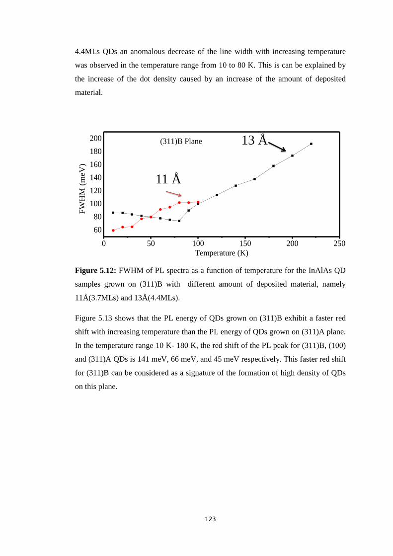
123
4.4MLs QDs an anomalous decrease of the line width with increasing temperature
was observed in the temperature range from 10 to 80 K. This is can be explained by
the increase of the dot density caused by an increase of the amount of deposited
material.
Figure 5.12: FWHM of PL spectra as a function of temperature for the InAlAs QD
samples grown on (311)B with different amount of deposited material, namely
11Å(3.7MLs) and 13Å(4.4MLs).
Figure 5.13 shows that the PL energy of QDs grown on (311)B exhibit a faster red
shift with increasing temperature than the PL energy of QDs grown on (311)A plane.
In the temperature range 10 K- 180 K, the red shift of the PL peak for (311)B, (100)
and (311)A QDs is 141 meV, 66 meV, and 45 meV respectively. This faster red shift
for (311)B can be considered as a signature of the formation of high density of QDs
on this plane.
0 50 100 150 200 250
60
80
100
120
140
160
180
200
FW
HM
(m
eV
)
Temperature (K)
(311)B Plane 13 Å
11 Å

124
Figure 5.13: Temperature dependence of the PL peak energy for QDs samples
grown on different substrate orientations, namely (100), (311)A, (311)B.
For (311)A sample there is a peak at around 2.3 eV which could be due to the
AlGaAs matrix. The appearance of this peak is probably due to the low density of
QDs formed on this plane. The PL intensity of AlGaAs matrix decreases drastically
when the temperature changes from 10 to 80 K, contrary to that of QDs which
persists up to 180 K (see Figure 5.14). This fast quenching with temperature can be
explained by the decrease of the degree of confinement.
Figure 5.14: PL intensity as a function of temperature for InAlAs QDs and AlGaAs
matrix for the (311)A sample.
0 50 100 150 200 250
1.65
1.70
1.75
1.80
1.85
En
erg
y (
eV
)
Temperature (K)
(100) Plane
(311)A Plane
(311)B Plane

125
In conclusion, the increase of the amount of Al0.35In0.65As material to form QDs
resulted in better optical efficiency for dots grown on high index planes. The best
structure in terms of optical output consisted of 13 Å (4.4 MLs)
Al0.35In0.65As/Al0.45G0.55As grown on (311)B GaAs substrate. Therefore the above
(311)B structure has been chosen to investigate the effect of the confining barrier
on the QDs optical quality.
5.3 EFFECT OF THE AlGaAs CARRIER CONFINING
POTENTIAL ON THE EMISSION ENERGY OF (311)B QDS
It is important to point out that the optical properties of (100) and (311)A 4.4 MLs Å
Al0.35In0.64As QDs grown on AlGaAs matrix with different Al percentages (25, 35,
45, and 55 %) are inferior to (311)B QDs counterpart with same Al percentage.
Therefore, the results presented in the following section are limited to the study of
the effect of the confining potential barrier on the optical properties of 4.4MLs
Al0.35In0.64As QDs on AlyGa1-yAs QDs with y=0.25, 0.35, 0.45 and 0.55 grown on
(311)B plane.
5.3.1 INTRODUCTION
For InAs QDs, it is well known that a high temperature stability of their optical
properties can be achieved owing to deep localization of carriers in a matrix whose
band gap is wider than that in GaAs60
.
A. Polimeni et al61
carried out a systematic study of the PL properties of
InAs/AlyGa1-yAs QDs over the Al compositional range y = 0 – 0.8 as a function of
temperature from 10 to 290 K. For an Al content greater than 15%, the QD PL
integrated intensity quenches very slowly with increasing temperature by less than
an order of magnitude. This was explained by the fact that the AlGaAs energy levels
are too distant from the dot ground state to have an appreciable thermal population.

126
The corresponding excitonic energy position has been calculated to be more than 400
meV away from the dot emission energy for y = 0.3. In contrast, for shallower
confining potentials (y = 0 and 0.15) the barrier may play an important role in the
thermal decrease of the QD PL. The PL signals of dots embedded in GaAs and
Al0.15Ga0.85As matrices decrease by factors of 200 and 80, respectively in the
temperature range 10-290 K.
5.3.2 EXPERIMENTAL RESULTS AND ANALYSIS
The PL signal from QDs is known to quench at different temperatures due to the
carrier loss which takes place through the mechanism of thermal excitation of
electron-hole pairs into the Al1-xGaxAs barriers. For this mechanism, the carrier loss
will be reduced or eliminated by increasing the activation energies, and this could be
achieved by increasing the Al percentage of the barriers, or by increasing the indium
concentration in the QDs. The latter is limited by the amount of strain which can be
incorporated. In this section, an investigation of In0.65Al0.35As QDs grown on
AlGaAs matrix with different Al concentrations have been carried out.
The features of the four studied samples in this section are shown in Table 5.3. A
200 nm thick GaAs buffer layer and a 300 nm thick AlyGa1−yAs layer were grown by
MBE at 600 °C on a (311)B GaAs substrate. Then the temperature was lowered to
450 °C and a 4.4MLs InAlAs layer was deposited to form QDs. Finally a 50nm thick
AlyGa1−yAs cap layer was deposited. The Al mole fraction (y) is chosen to be 0.25,
0.35, 0.45, and 0.55.

127
Table 5.3: Investigated samples having different Al content in the confining barrier.
Sample Number Substrate Al mole fraction
NU1683
QD0.25
(311)B
(311)B 25%
NU2735
QD0.35
(311)B
(311)B 35%
NU2738
QD0.45
(311)B
(311)B 45%
NU2745
QD0.55
(311)B
(311)B 55%
By increasing the Al percentage in matrix, the energy difference between the InAlAs
QDs and the AlyGa1−yAs barrier state is increased. This gives greater confinement of
carriers in the QD. As a result, thermal activation effects could be less serious and
therefore it may be possible to extend the PL emission of the InAlAs QD system to
room temperature.
Figure 5.15 shows the PL spectra at 8 K for (311)B InAlAs QDs deposited on
AlGaAs matrices containing different Al concentrations. The energy of QDs shows a
small blue shift with increasing Al content in the matrix (Figure 5.16). This could be
due to the diffusion of Al from the AlGaAs matrix with higher Al into the QDs
resulting in enhanced Al incorporation in the InAlAs dots. The integral intensity has
a strong dependence on the Al percentage in matrix. The PL properties of these QDs
are summarized in Table 5.4.

128
Figure 5.15: PL spectra of (311)B InAlAs QDs grown on AlGaAs matrix with
different Al concentrations.
Table 5.4: The PL properties of Al0.35In0.65As / AlyGa1−yAs QDs.
Al
(%)
QD PL
Energy
(eV)
PL Energy of
AlyGa1−yAs matrix
(eV)
Difference between QD
energy and AlGaAs
matrix energy
(meV)
PL
intensity/
PL intensity
of
QD0.25
(311)B
25 1.68 1.83 150 1
35 1.71 1.97 260 10
45 1.8 2.04 240 13
55 1.82 2.15 330 11
1.5 1.6 1.7 1.8 1.9 2.0 2.1
Energy (eV)
Al=55%
Al=45%
Al=35%
Al=25%
x10
PL
(a.u
)(311)B Plane

129
Figure 5.16: QD PL energy as function of Al percentage in matrix.
To further investigate the effect of the different Al concentration in matrix on the PL
efficiency of the InAlAs QDs, the PL intensity (PLI) over the temperature range 10-
220 K was determined for all four samples. The temperature dependence of the PLI
for all four samples with different Al concentrations in matrix is shown in Figure
5.17.
The PLI of sample QD0.25
(311)B remains approximately constant up to 30 K, and then
decreases by a factor of 1654 at 200K. This behaviour is typical for InAs/GaAs QDs
and has been attributed to the thermal escape of the carriers from the QDs34, 62
. When
the Al content in GaAlAs matrix increases to 35% in sample QD0.35
(311)B, the PL
quenching improved from 200K to 220 K. The PL signal decreased by a factor of
644 in the temperature range 10-220 K. Further incorporation of Al to 45 % in
sample QD0.45
(311)B, the PLI decreases by a factor of less than 172 in similar
temperature range. The data presented in Figure 5.17 clearly show that the
temperature above which quenching of the PL occurs increases with the Al content
in the GaAlAs matrix. For the sample with of 55% Al led to an improvement of the
PL at low temperature as comparing to sample with 25% Al content. However, with
25% 35% 45% 55%
1.68
1.72
1.76
1.80
1.84
En
erg
y (
eV
)
Al %
(311)B Plane

130
increasing temperature a faster quenching appears which may be explained by an
increase of non-radiative defects that have been created due to the higher Al content
used.
In comparison with sample QD0.25
(311)B, at 100 K the PL intensity of sample
QD0.45
(311)B is approximately 50 times higher as shown in Figure 5.18. These ratio
values are enhanced with increasing temperature; an enhancement of the
luminescence efficiency, particularly at high temperatures is highly desirable for
optoelectronic applications.
Figure 5.17: The temperature dependence of PL intensity of (311)B QDs grown on
AlGaAs matrix with different Al concentrations. The lines are guide for the eyes.
0 50 100 150 200 250
PL
inte
nsi
ty (
a.u
)
Temperature (K)
25%
35%
45%
55%
(311)B Plane

131
Figure 5.18: The ratio of PL intensity of samples QD0.35
(311)B, QD0.45
(311)B, and
QD0.55
(311)B to sample QD0.25
(311)B as a function of temperature.
In conclusion, an AlGaAs confining barrier with 45% Al is found to provide higher
optical efficiency of QDs grown on all planes (only results on (311)B are reported in
this section). The optimum structure that gives the best optical properties consists of
4.4MLs Al0.35In0.65As QDs/AlyGa1-yAs with y = 0.45 grown on (311)B wafer.
Therefore this structure grown on the (311)B plane has been chosen to investigate
the effect of the growth temperature (450 0C, 500
0C, 550
0C) on the QDs optical
efficiency.
0 50 100 150 2000
200
400
600
800
1000
1200
1400
PL
Inte
nsi
ty r
ati
o
Temperature (K)
35%
45%
55%
(311)B Plane

132
5.4 EFFECT OF GROWTH TEMPERATURE ON OPTICAL
EFFICIENCY OF (311)B InAlAs QDs GROWN ON Al0.45Ga0.55As
MATRIX
Al0.35In0.65As/Al0.45Ga0.55As (311)B QDs samples were grown under the same
condition and have the same layer structure as the previous samples except that the
deposited Al0.35In0.65As QDs were grown at three different temperatures, namely 450
0C, 500
0C, and 550
0C.
The details of the three investigated samples in this section are shown in Table 5.5.
It is worth pointing out that the 4.4 MLs Al0.35In0.65As QDs grown on (100) and
)311(A planes at a growth temperature of 500 0C do not display any luminescence
signal. The reason(s) of their poor optical quality is not clear at this stage. However,
their optical properties were recovered and improved when grown at 550 0C (i.e.
better than QDs grown at 450 0C) but still inferior than the (311)B QDs.. The results
presented in the following section are therefore limited to the study of the effect of
the growth temperature on the optical properties of (311)B QDs .
Table 5.5: Al0.35In0.65As/Al0.45Ga0.55As (311)B QDs samples grown at various
temperatures.
Sample Number Substrate Growth temperature
NU2738
QD450
(311B)
(311)B 450 0C
NU2754
QD500
(311B)
(311)B 500 0C
NU2757
QD550
(311B)
(311)B 550 0C
Figure 5.19 shows PL spectra at 8 K for (311)B samples grown at various
temperatures. The peak position, FWHM and the integral intensity have a strong

133
dependence on the growth temperature. The PL properties of these QDs are
summarized in Table 5.6.
Figure 5.19: PL spectra of Al0.35In0.65As/Al0.45Ga0.55As QDs grown at different
growth temperatures on (311)B GaAs substrate orientation.
When the growth temperature increased from 450 0C to 500
0C, the peak position of
QDs shifted to low energy, whereas the QD peak shifted to high energy when growth
temperature was 550 0C. This red energy shift has been observed for InAs/GaAs
QDs63-65
and was explained by the increase of the surface migration of In atoms with
increasing temperature. The distance between the In atoms which have assembled to
form one dot is increased, and this results in the formation of larger dots.
The blue-shift of the peak energy of the QDs grown at 550 0C might be due to the
emission related to the excited electron states in big QDs66
. The other possible
explanation of the blue-shift is the thermally enhanced intermixing of In and Ga
atoms at the QD/matrix interface.
The PL intensity of QDs grown at the highest temperature is four times larger than
the PL intensity of QDs grown at the lowest temperature. It is believed that the high
intensity achieved at 550 0C is due to fewer defects formed at the higher growth
temperature than the lower growth temperature. This argument is supported by the
fact that the PL from samples grown at high growth temperature quenches at much
higher temperature of 290 K (see Figure 5.20).
1.6 1.7 1.8 1.9 2.0
(311)B Plane
Energy (eV)
450 0C
500 0C
550 0C
PL
(a.u
)

134
Table 5.6: Summary of PL properties of Al0.35In0.65As/Al0.45Ga0.55As (311)B QDs
samples grown at various temperatures.
Growth Temperature FWHM
(meV)
PL Energy
(eV)
PL intensity /
PL intensity (QD450
(311B))
450 0C 86 1.799
1
500 0C 113 1.72
1.2
550 0C 128 1.86
4.15
Figure 5.20: Temperature dependence of PL intensity of (311)B
Al0.35In0.65As/Al0.45Ga0.55As QDs grown at different growth temperatures. The lines
are guide for the eyes.
In conclusion, an increase of the growth temperature results in a significant optical
improvement. A temperature of 550 0C to grow AlInAs was the optimum condition
to achieve high optical efficiency QDs emitting in the visible.
0 50 100 150 200 250 300
(311)B Plane
Ln
(P
LI)
(a.u
)
Temperature (K)
450 0C
500 0C
550 0C

135
5.5 CONCLUSION
In summary, Al0.35In0.65As QDs formed under different growth conditions on (100)
and high-index GaAs substrates by MBE have been investigated. PL results
confirmed that the formation of QDs occurs for all substrate orientations. The PL
measurements revealed differences in the optical properties that are caused by
substrate orientation effects. The PL emission energies of QDs grown on high Miller
index surfaces are found to be strongly dependent on the atomic terminated surface
[A (Ga face) or B (As face)] of the substrate.
The optical quality of the 3.7 MLs AlInAs QDs on high index planes is found to be
inferior to that of (100) QDs. Due to the fact that all substrate orientations were
grown simultaneously using growth conditions that are optimised for (100)
substrates, the inferior optical quality of QDs grown on high index planes could
therefore be due to the non-optimized growth conditions and layer structure. By
increasing the deposited Al0.35In0.65As material to 4.4MLs, the optical efficiency of
QDs grown on (311)B improved, however the optical efficiency of (311)A QDs was
still inferior to (100) QDs. The (100) QDs PL efficiency was not enhanced but the
FWHM decreased. The lower density of QDs on the (311)A orientation could be
responsible for the observed low emission efficiency. It is found that the
improvement of PL efficiency from (311)B QDs is accompanied by an increase of
the FWHM. This can be understood in terms of fluctuation of their size distribution.
By increasing the confinement barriers, i.e. increasing the Al content of the matrix to
45%, the temperature-dependent PL study shows that the PL thermal quenching of
the QDs occurs at higher temperatures due to the higher confinement potential. An
improvement of the optical quality accompanied by a blue shift from (311)B QDs
has been observed by increasing the growth temperature from 450 0C to 550
0C.

136
REFERENCES
1 D. J. Eaglemann, and M. Cerullo, Physical Review Letters, 64, 1943 (1990).
2 D. Leonard, S. Fafard, K. Pond, Y. H. Zhang, J. M. Merz, and P. M. Petro, Journal
of Vacuum Science and Technology B, 12, 2516 (1994).
3 J. Y. Marzin, J. M. Gerald, A. Izrael, D. Barrier, and G. Bastard, Physical Review
Letters,73, 716 (1994).
4 F. Hatami, N. N. Ledentsov, M. Grundmann, J. Bohrer, F. Heinrichsdor, M. Beer,
D. Bimberg, S. S. Ruvimov, P. Werner, U. Gosele, J. Heydenreich, U. Richter, S.V.
Ivanov, B. Y. Meltser, P. S. Kopev, and Z. Alferov, Applied Physics Letters, 67, 656
(1995).
5 A. Kurtenbach, K. Eberl, and T. Shitara, Applied Physics Letters, 66, 361 (1995).
6 H. Marchand, P. Desjardins, D. Guillon, J. Paultre, Z. Bougrioua, R. Yip, and R.A.
Masut, Applied Physics Letters, 71, 527 (1997).
7 S. Fafard, Z. Wasilewski, J. Mccrey, S. Raymond, and S. Charbonneau, Applied
Physics Letters, 68, 991 (1996).
8 H. Li, J. Wu, B. Xu, J. Liang, and Z. Wang, Applied Physics Letters,72, 2123
(1998).
9 R. Leon, S. Fafard, D. Leonard, J. L. Merz, and P. M. Petroff, Science, 274, 1350
(1996).
10 R. Heitz, M. Veit, N. N. Ledentsov, A. Hoffmann, D. Bimberg, V. M. Ustinov, P.
S. Kop’ev, and Zh. I. Alferov, Physical Review B, 56, 10435 (1997).
11 W. Zhou, B. Xu, H. Z. Xu, F. Q. Liu, J. B. Liang, Z. G. Wang, Z. Z. Zhu, and G.
H. LI, Journal of Electronic Materials, 28, 5, (1999).

137
12 X. M. Lu, Y. Izumi, M. Koyama, Y. Nakata, S. Adachi, and S. Muto, Journal of
Crystal Growth, 322, 6, (2011).
13 R. Leon, S. Fafard, D. Leonard, J. L. Merz, and P. M. Petroffc, Applied Physics
Letters, 67, 521 (1995).
14 A. F. Tsatsul'nikov, A. Yu. Egorov, P. S. Kop'ev, A. R. Kovsh, N. N. Ledentsov,
M. V. Maximov, A. A. Suvorova, V. M. Ustinov, B. V. Volovik, A. E. Zhukov, M.
Grundmann, D. Bimberg, and Zh. I. Alferov, Applied Surface Science, 123, 381
(1998).
15 H. Y. Liu, B. Xu, J. J. Qian, X. L. Ye, Q. Han, D. Ding, J. B. Liang, X. R. Zhong,
and Z. G. Wang, Journal of Applied Physics, 90, 2048 (2001).
16 B. L. Liu, Z. Y. Xu, H. Y. Liu, and Z. G. Wang, Journal of Crystal Growth, 220,
51 (2000).
17 I. Alghoraibi, T. Rohel, N. Bertru, A. Le Corre, A. Létoublon, P. Caroff, O.
Dehaese, and S. Loualiche, Journal of Crystal Growth, 293, 263 (2006).
18 B. A. Joyce, and D. D. Vvedensky, Materials Science and Engineering: R:
Reports, 46, 127 (2004).
19 L. Sfaxi, L. Bouzaiene, H. Sghaier, and H. Maaref, Journal of Crystal Growth,
293, 330 (2006).
20 M. Henini, Nanoscale Research Letters, 1, 32 (2006).
21 Y. Temko, T. Suzuki, P. Kratzer, and K. Jacobi, Physical Review B, 68,
165310 (2003).
22 T. Suzuki, Y. Temko, and K. Jacobi, Applied Physics Letters, 80, 4744 (2002).

138
23 K. Jacobi, Progress in Surface Science, 71, 185 (2003).
24 D. I. Lubyshev, P. P. Gonzalez-Borrero, E. Marega, J. E. Petitprez, and P.
Basmaji, Journal of Vacuum Science and Technology B, 14, 2212 (1996).
25 M. C. Xu, Y. Temko, T. Suzuki, and K. Jacobi, Physical Review B, 71, 075314
(2005).
26 M. C. Xu, Y. Temko, T. Suzuki, and K. Jacobi, Surface Science, 576, 89 (2005).
27 R. Notzel, N. N. Ledentsov, L. Daweritz, K. Ploog and M. Hohenstein, Physical
Review B, 3507 (1993).
28 S. Zhong-Zhe, L. Feng-Qi, W. Ju, Y. Xiao-Ling, D. Ding, X. Bo, L. Ji-Ben, and
W. Zhan-Guo, Physica E, 8, 164 (2000).
29 S. C. Fortina, S. Sanguintti, E. Grilli, M. Guzzi, M. Henini, A. Polimeni, and L.
Eaves, Journal of Crystal Growth, 187, 126 (1998).
30 M. Henini, III-Vs Rev., 11, 48 (1998).
31 C. Lobo, and R. Leon, Journal of Applied Physics, 83, 4168 (1998).
32 P. P. Gonzilez-Borrero, D. I. Lubyshev, E. Marega Jr, E. Petitprez, and P.
Basmaji, Journal of Crystal Growth, 169, 428 (1996).
33 Z. Y. Xu, Z. D. Lu, X. P. Yang, B. Z. Zheng, J. Z. Xu, W. K. Ge, Y. Wang, J.
Wang, and L. L. Chang, Superlattices and Microstructures, 23, 381 (1998).
34 Z. Xu, Z. Lu, X. Yang, Z. Yuan, B. Zheng, J. Xu, W. Ge, Y. Wang, J. Wang, and
L. Chang, Physical Review B, 54, 11528 (1996).

139
35
S. Fafard, Z. R. Wasilewski, C. Ni. Allen, D. Picard, M. Spanner, J. P. Mccaffrey,
and P. G. Piva, Physical Review B, 59, 15368 (1999).
36 J. He, Y. Zhang, B. Xu, and Z. Wang, Journal of Crystal Growth, 247, 49 (2003).
37 B. Liang, Z. Wang, Y. Mazur, V. Strelchuck, K. Holmes, J. Lee, and G. Salamo,
Nanotechnology, 17, 2736 (2006).
38 W. Jiang, H. Xu, B. Xu, X. Ye, W. Zhou, D. Ding, J. Liang, and Z. Wang,
Physica E, 8, 134 (2000).
39 A. Polimeni, M. Henini, A. Patane, L. Eaves, and P. Main, and G. Hill, Applied
Physics Letters, 73, 1415 (1998).
40 S. Sanguinetti, G. Chiantoni, E. Grilli, M. Guzzi, M. Henini, A. Polimeni, A.
Patane, L. Eaves, and P. Main, Europhysics Letters, 47 (6), 701 (1999).
41 D. Leonard, M. Krishnamurthy, S. Fafard, J. Merz, and P. Petroff, Journal of
Vacuum Science and Technology B, 12, 1063 (1994).
42 D. Leonard, M. Krishnamurthy, C. M. Reaves, S. P. Denbaars, and P. M. Petroff,
Applied Physics Letters, 63, 3203 (1993).
43 M. Colocci, F. Bogani, L. Carraresi, R. Mattolini, A. Bosacchi, S. Franchi, P.
Frigeri, M. Rosa-Clot, and S. Taddei, Applied Physics Letters, 70, 3140 (1997).
44 A. Polimeni, A. Patane, M. Capizzi, F. Martelli, L. Nasi, and G. Salviati, Physical
Review B, 53, 4213 (1996).
45 S. Sanguinetti, G. Chiantoni, E. Grilli, M. Guzzi, M. Henini, A. Polimeni, A.
Patane, L. Eaves, and P.C. Main, Materials Science and Engineering B, 74, 239
(2000).

140
46
G. M. Guryanov, G. E. Cirlin, V. N. Petrov, N. K. Polyakov, A. O. Golubok, S.
Tipissev, V. B. Gubanov, Yu. B. Samsonenko, N. N. Ledentsov, V. A. Shchukin, M.
Grundmann, D. Bimberg, and Zh. I. Alferov, Surface Science, 352, 651 (1996).
47 D. Gammon, S. Rudin, T. L. Reincke, D. S. Katzer, and C. S. Kyono, Physical
Review B, 51, 16785 (1995).
48 Y. T. Dai, J. C. Fan, Y. F. Chen, and R. M. Lin, S. C. Lee, and H. H. Lin, Journal
of Applied Physics, 82, 4489 (1997).
49 M. Hjiri, F. Hassen, H. Maaref, B. Salem, G. Bremond, O. Marty, J. Brault, and
M. Gendry, Physica E, 17, 180 (2003).
50 R. Songmuang, S. Kiravittaya, M. Sawadsaringkarn, S. Panyakeow, and O. G.
Schmidt, Journal of Crystal Growth, 251, 166 (2003).
51 Y. P. Varshni, Physica (Amsterdam), 34, 149 (1967).
52 H. Wang, D. Ning, and L. Feng, Journal of Crystal Growth, 209, 630 (2000).
53 D. K. Gaskill, N. Bottka, L. Aina, and M. Mattingly, Applied Physics Letters, 56,
1269 (1990).
54 S. Sanguinettia, A. Miottoa, S. Castiglionia, E. Grillia, M. Guzzia, M. Henini, A.
Polimeni, A. Patane, L. Eaves, and P. Main, Microelectronics Journal, 30, 419
(1999).
55 D. I. Lubyshev, P. P. Gonzalez-Borrero, E. Marega, and P. Basmaji, Journal of
Vacuum Science and Technology B, 14(3), (1996).
56 S. Sanguinetti, S. Fortina, A. Miotto, E. Grilli, M. Guzzi, M. Henini, A. Polimeni,
and L. Eaves, Thin Solid Films, 336, 9 (1998).

141
57
W. Zhou, Z. M. Zhu, F. Q. Liu, B. Xu, H. Z. Xu, and Z. G. Wang, Journal of
Crystal Growth, 200, 608 (1999).
58 C. Loboa, and R. Leon, Journal of Applied Physics, 83, 4168 (1998).
59 B. G. Orr, D. Kessler, C. W. Snyder, and L. Sander, Europhysics Letters, 19, 337
(1992).
60 Y. S. Kim, U. H. Lee, D. Lee, S. J. Rhee, Y. A. Leem, H. S. Ko, D. H. Kim, and J.
C. Woo, Journal of Applied Physics, 87, 241 (2000).
61 A. Polimeni, A. Patane, M. Henini, L. Eaves, and P. Main, Physical Review B, 59,
5064 (1999).
62 S. Sanguinetti, M. Henini, M. Grassi Alessi, M. Capizzi, P. Frigeri, and S. Franchi,
Physical Review B, 60, 8276 (1999).
63 T. Kaizu, and K. Yamaguchi, Japanese Journal of Applied Physics, 40, 1885
(2001).
64 Y. Nakata, Y. Sugiyama, and M. Sugawara, Semiconductor and Semi-metals,
Academic Press, San Diego (1999).
65 V. G. Dubrovskiia, G. E. Cirlinb, Yu. G. Musikhina, Yu. B. Samsonenkob, A. A.
Tonkikha, N. K. Polyakovb, V. A. Egorovb, A. F. Tsataul’nikova, N. A.
Krizhanovskayaa, V. M. Ustinova, and P. Wernerc, Journal of Crystal Growth, 267,
47 (2004).
66 S. P. Guo, A. Shen, Y. Ohno, and H. Ohno, Physica E, 2, 672 (1998).

142
CHAPTER 6: ANNEALING EFFECT ON InAlAs
QUANTUM DOTS GROWN ON (100), (311)A, (311)B
GaAs SUBSTRATES

143
This chapter reports the effect of the post growth annealing process on the optical
properties of InAlAs self-organized quantum dots (QDs) grown on different GaAs
substrate orientations, namely (100), (311)A, and (311)B.
6.1 INTRODUCTION
As reported in the previous chapter the self-organized InAlAs QDs are grown by
MBE using the Stranski-Krastanow growth mode, which does not involve any
substrate patterning process. Although these QDs have a well-defined shape, their
random nucleation in single layer results in a broad distribution of QDs size, and
limit their practical applications. Further developments in the use of QD structures
for devices such as zero dimensional (0D) lasers are dependent on the achievement
of tunability of dot dimensions and size dispersion in order to both control the
wavelength and reduce the linewidth of the luminescence emission. Therefore, there
is a need to control the size uniformity in QDs. In addition, most device processes
also include high temperature annealing, and therefore it is very important to
investigate the behavior of QDs during thermal treatment.
The post-growth thermal treatment is frequently used to modify the structural and
optical properties of self-assembled InAs and InGaAs QDs1,2
. These effects should
be either strongly avoided or, on the opposite, can be used intentionally to modify
the properties of the QD structures.
The effects of post-growth thermal annealing on QDs include a blue shift of
interband transition energy and narrowing of the PL line width. Although these
phenomena can be described by inter-diffusion between the QD and the barrier, the
detailed mechanisms are still not very clear. There are considerable reports available
in literature that have studied these phenomena but the PL data are different due to
the different kinds of QD structures.
The inter-diffusion process depends on several factors like the quality of interface
between dots and barrier, the density of defects such as vacancies, interstitials, and
dislocations. The inter-diffusion mechanism is therefore closely correlated with the
growth process of QDs (temperature, growth rate, growth plane, capping layer
etc)3,4
.

144
To my knowledge there is no reported work about the influence of annealing on
InAlAs QDs grown on the conventional (100) and high index plane except the data
reported by C. Lobo et al 5 on dots grown on (100) plane.
C. Lobo et al5 have examined the effect of post-growth annealing on the inter-
diffusion and the luminescence emission from red and infrared emitting self-
assembled III–V quantum dots. Three different combinations of dot/barrier materials
have been investigated: InAlAs/AlGaAs, InGaAs/AlGaAs and InGaAs/GaAs. In all
cases, thermal intermixing was found to result in significant blue shifts of the PL
emission. In addition, narrowing of the linewidth of the inhomogeneously broadened
PL peak was observed. Both effects were found to be strongly dependent on the
material system and average dot size. The extent of blue shifting increases with dot
size across all material systems. The maximum blue shift was observed at an
annealing temperature of 900 °C and ranges from 77 meV for the smaller
InAlAs/AlGaAs QDs (28.6 nm) to 160 meV for the InGaAs/AlGaAs (46 nm) QDs.
The PL emission from the single layer and multilayer stack of InGaAs/ GaAs (29.5
nm ) QDs showed a blueshift of 97 meV after annealing at 900 °C for 30 s. In
addition, it was found that the magnitude of the narrowing of the linewidth to be very
sensitive to the nature of the QDs and the confining barrier, ranging from 50 meV for
InAlAs/AlGaAs QDs to 30 meV for InGaAs/GaAs QDs, and just 10 meV for
InGaAs/AlGaAs QDs annealed at 900 °C. This difference in linewidth narrowing
suggests that both the magnitude and direction of the composition gradient across the
dot/barrier interface are important in determining the effect of inter-diffusion on the
PL emission.
Z. Zhang et al6 have investigated the rapid thermal annealing (RTA) of InAs QDs
under different strain layers (InxAl1-xAs/In0.2Ga0.8As combination overgrowth). The
photoluminescence measurements demonstrated that the InAs QDs experience an
abnormal variation during the course of RTA. The InAs QDs PL peak is blue shifted
up to 260 meV after annealing at 800 0C. The magnitude of energy blue shift and
change of shape of PL spectra was found to depend on the thickness of InxAl1-xAs
layer. In order to explain the variation of the PL spectra (in terms of FWHM,
intensity and energy), they claimed that the InAs QDs transformed into InAlAs and
InGaAlAs QDs depending on the annealing temperature and InxAl1-xAs capping
layer.

145
Z. Zaaboub et al7 studied the effect of post-growth rapid thermal annealing on the PL
properties of low density InAs/GaAs QDs emitting around 1170 nm. For an
annealing temperature of 650 °C for 30 s, the emission wavelength and the inter-
sublevel spacing energies remained unchanged while the integrated PL intensity
increases. For higher annealing temperatures, blue shift of the emission energy up to
172 meV together with a decrease in the inter-sublevel spacing energies from 67 to
33 meV were shown to occur due to the thermal activated In–Ga inter-diffusion. The
appearance of an additional excited state for annealing temperatures higher than 650
°C suggests a variation of the intermixed QDs' volume/diameter ratio toward QDs'
enlargement.
W. Jiang et al8 investigated the surface morphology and optical properties of
InGaAs/GaAs QDs subjected to different annealing temperatures by TEM and PL
techniques. The PL peak position is almost constant when the annealing temperature
is 650 0C, indicating a weak inter-diffusion. A clear blue shift of the PL spectrum
due to In/Ga inter-diffussion occurs at 700 0C, along with a narrowing of linewidth
and an increase of PL intensity. TEM results show that higher annealing
temperatures (higher than 850 0C) lead to the degradation of QD material and some
clusters are formed which destroy the QDs significantly. The degradation is caused
by surface roughing and formation of large clusters, due to the strong inter-diffusion
of In, Ga atoms and strain relaxation.
I. J. Guerrero Moreno et al9 have employed PL to study the effect of the annealing at
640 0C for 2 hours on MBE grown InAs QDs capped with different capping
materials, such as GaAs and Al0.3Ga0.7As. They have shown that thermal annealing
initiates the shift of PL peak positions into the high energy spectral range and the
values of this blue shift are found to be dependent on the composition of capping
layers. Furthermore, I. J. Guerrero Moreno and co-workers have investigated the
temperature dependence of the PL peak positions of QDs in the range of 10–300 K
and compared it with the temperature shrinkage of the band gap of bulk InAs crystal.
This study allowed them to investigate the efficiency of the Ga(Al)/In inter-diffusion
processes in relation to the nature/composition of the capping layer. Experimental
and fitting parameters obtained for InAs QDs have been compared with known ones
146
for the bulk InAs crystal. It is revealed that the efficiency of the Ga(Al)/In inter-
diffusion depends essentially on the composition of the capping layer.
It has been reported that strain free QDs can be obtained by using the modified
droplet epitaxy (MDE) technique10-12
. The formation of QDs by MDE is different
than the well-known Stranski-Krastanov method. T. Mano et al13
have employed PL
and cross-sectional high-angle annular dark field scanning transmission electron
microscopy (HAADF-STEM) to investigate the effects of post-growth annealing on
structural and optical properties of self-assembled ring-shaped GaAs QDs grown by
MDE. Negligible structural changes of the QDs were observed after the annealing
process up to 800 0C while the intensity of PL emission increased drastically. The
annealed laser structure with three layers of the ring-shaped QDs showed photo-
pumped laser action with clear threshold at 77 K.
S. Sanguinetti et al14
carried out a systematic study of the post growth annealing
effects on the optical properties of self-assembled GaAs/AlGaAs QDs grown by
MDE. The process of post-annealing strongly affects the optical properties of the
MDE QDs. The post-annealing creates structural modifications of the MDE QD
heterostructures by promoting the intermixing of the group III elements. The
assessment of the modifications of the QD eigenstates and of the QD environment
has been performed via optical measurements. They determined an inter-diffusion
length (l) of Ga and Al (l = 1 nm) at relatively low annealing temperatures (520 0C),
with a relatively slow increase with the annealing temperature. Low temperature
growth used during QDs formation lead to the presence of a high concentration of
out-of-equilibrium group III vacancies which in turn lead to the strong inter-
diffusion process during the annealing. By applying the rate equation model they
demonstrated that the quenching of PL with temperature in the case of as-grown
samples is due to the escape of carriers from the GaAs QDs to the WL. However, for
the annealed samples the PL quenching is accounted for by the excitation of carriers
from QDs directly into the AlGaAs barrier.
S. Malik et al15
have observed blue shift in the PL emission energies from an
ensemble of self-assembled InAs QDs as a result of post-growth thermal annealing.
Enhancement of the integrated PL emission and narrowing of the full width half-

147
maxima (from 55 to 12 meV) occur together with blue shifts up to 300 meV at
annealing temperatures up to 950 °C. Evidence that the structures remain as dots at
this high annealing temperature comes from the observation of level filling and
photoluminescence excitation studies which reveal longitudinal phonon (LO) peaks
occurring at multiples of 30 meV from the detection energies.
H. Park et al16
have employed PL and TEM to study the effects of multi-steps RTA
on the self-assembled InAs QDs, which were grown by MBE. Post-growth multi-
steps RTAs are as follows: one step (20 s at 750 0C), two steps (20 s at 650
0C, 20 s
at 750 0C), three steps (30 s at 450
0C, 20 s at 650
0C, 20 s at 750
0C). They found
that significant narrowing of the luminescence linewidth (from 132 to 31 meV) from
InAs QDs occurs together with about 150 meV blue shift by two-steps annealing as
compared to as-grown InAs QDs. Analysis of TEM data confirm the existence of the
dots under one- and two-steps annealing but the disappearance of the dots by three-
steps annealing. Comparing with the samples under only one-step annealing, they
demonstrate a significant enhancement of the inter-diffusion in the dot layer under
multi-steps annealing.
S. J. Xu et al17
studied the effect of RTA post-growth thermal process on the
structural and optical properties of the self-assembled InAs QDs grown on GaAs
substrates by MBE. It was found that significant narrowing of the luminescence
linewidth (from 78.9 to 20.5 meV) from the InAs dot layer occurs together with
about 260 meV blueshift at annealing temperatures up to 850 °C. This large blue
shift was explained to be due to the thick SiO2 capping layer used during the
annealing process. Images of High Resolution TEM (HRTEM) show the existence
of dots under lower annealing temperatures but disappearance of the dots annealed at
850 °C. The excited-state-filling experiments on the samples show that the
luminescence of the samples annealed at 850 °C exhibits quantum well-like
behavior, while no excited-state emissions were observed even at high excitation
power. This also provides evidence of the disappearance of the QDs at high
annealing temperatures. Comparing with a reference quantum well, they
demonstrated significant enhancement of the inter-diffusion in the dot layer.

148
S. Martini et al18
investigated In segregation from In0.10Ga0.90As/GaAs quantum
wells grown on different GaAs (001) substrates with a miscut angle of 0° (nominal),
2°, 4° and 6° towards [110] using low temperature PL. Extra emission at low energy
was only observed for the nominal sample and was related to In segregation. Its
absence from the PL spectrum of quantum wells grown on vicinal surfaces is a
strong indication that In segregation is modified on this type of surface. This feature
was related to the trapping of free excitons by slightly In-rich islands that were
present at the second interface as a result of In segregation. The presence of a high
density of steps limits the surface migration of the adatoms.
F. Guimaraes et al19
studied the influence of surface structure and morphology on
indium segregation in InGaAs/GaAs quantum well structures grown by MBE on
(100), (311)A and (311)B GaAs surfaces. They reported that indium surface
segregation in (311)A GaAs surface is smaller than in the (100) and (311)B
orientations. They state that surfaces with high step structures or density, such as in
the case of (311)A surface, would favour the incorporation of indium at the step
edges and therefore reducing In segregation. In addition, they found that by using the
growth interruption technique at only the inverted GaAs-to-InGaAs interface In
segregation is reduced for all orientations. They explained this effect by a change in
the surface structure.
6.2 EXPERIMENTAL RESULTS AND ANALYSIS
The study of the annealing effect on the samples investigated in this section is the
samples that gave the best optical efficiency as discussed in the previous chapter.
The samples consisted of a 0.2 µm-thick GaAs buffer layer of which the first 0.1 µm
was grown at 580 °C and the remaining 0.1 µm at 600 °C. The temperature was kept
at 600 0C during deposition of the Al0.45Ga0.55As matrix layer. This was followed by
the deposition of 13Å Al0.35In0.65As strained layer at 550 0C for the formation of
QDs, a 50 nm Al0.45Ga0.55As, and 10 nm GaAs cap layer .
Post-growth annealing is performed using proximity capping, meaning an annealing
process involving a piece of GaAs substrate in close proximity to the sample

149
surface5,20
. The samples cut from the as-grown wafer were proximity capped and
RTA treated in argon ambient for 30 s at 600 oC, 700
oC, and 800
oC.
It is known that RTA of samples without any capping leads to surface degradation
due to As out diffusion. It is well established that the sample capping during post-
growth of strained InGaAs/GaAs multi quantum wells can critically influence the
results of the annealing procedure21
.
To remove the effects of any variations in annealing temperatures between samples,
all the samples were annealed simultaneously as a batch. PL measurements at 10 K
were performed on each of the samples prior to annealing, and then again following
the annealing process. Further anneals were then performed on the same samples
with the low temperature PL recorded after each anneal.
6.2.1 LOW TEMPERATURE PHOTOLUMINESCENCE OF ANNEALED
SAMPLES AT DIFFERENT TEMPERATURES
Figure 6.1 shows the 10 K PL spectra of as-grown, and 600 0C and 700
0C annealed
(100), (311)A, (311)B QD samples.
The peak PL energy of (100), (311)A, and (311)B as-grown samples are 1.744, 1.96,
and 1.859 eV with FWHM of 141, 65, 128 meV, respectively. The higher energy
observed for QDs formed on high-index surfaces is due to their smaller size than
those formed on the (100) substrate.
It is evident from figure 6.1 that almost no change of the peak position is observed
when the annealing temperature is 600 0C for QDs grown on (100) and (311)A
planes, while there is a small blue shift of 34 meV for (311)B dots. The FWHM of
PL spectra for 600 oC annealed samples have different behavior for different planes.
It decreases for QDs grown on (100) plane while it is constant for the QDs grown on
high index planes. However, all annealed QDs show an enhancement of PL
efficiency at this annealing temperature as demonstrated in Figure 6.1. By increasing
the annealing temperature to 7000C, (100) and (311)B QDs samples show a large
blue shift of 103 and 130 meV, respectively in their PL peak energy and a significant
narrowing of the PL linewidth as compared to the as-grown samples. The PL of
(311)A QDs shows a very small blue shift of 3meV as compared to the as-grown

150
sample. It is worth noting that there is a substantial increase in the integrated PL
intensity of all the samples annealed at 700 0C, as shown in Figure 6.1.
Table 6.1 gives a summary of luminescence emission parameters from as-grown and
700 0C annealed (100), (311)A, (311)B QDs.
Figure 6.1: 10 K PL spectra of as-grown and annealed QD samples grown on
different GaAs substrate orientations: (a) (100), (b) (311)B, (c) (311)A.
1.6 1.7 1.8 1.9 2.0
PL
(a.u
)
Energy (eV)
As-Grown
600 0C
700 0C
(100)
(a)
1.8 1.9 2.0 2.1
PL
(a.u
)
Energy (eV)
As-Grown
600 0C
700 0C
(311)A
(c)
1.6 1.7 1.8 1.9 2.0 2.1
PL
(a.u
)
Energy (eV)
As Grown
600c
700c (311)B
(b)

151
Table 6.1: Summary of photoluminescence emission parameters from (100), (311)A,
(311)B QDs. Blue shifts and reductions in FWHM refer to samples annealed at 700
°C for 30 s.
Growth
Plane
PL energy
(eV)
FWHM
(meV)
Blueshift
(meV)
Percentage of
Reduction in
FWHM
(100) 1.784 141 103 56%
(311)A 1.965 65 3 29%
(311)B 1.859 128 130 60%
RTA thermal treatment at 800 0C has also been performed. It was observed that the
PL of QDs disappears and the only peak present was due to the AlGaAs matrix. This
suggests that the QDs dissolve into the surrounding materials. Dissolution of QDs
after the RTA process at high temperature (850 0C for 50 s
17 or 950
0C for 30 s
15) has
previously been observed in InAs/GaAs QDs.
The blue shift with increasing annealing temperatures can be explained by the
interfacial diffusion between the InAlAs QDs and the AlGaAs barrier, which should
result in a change in the InAlAs QDs composition and an effective change in the
QDs size22
.
An obvious narrowing of the FWHM is observed ranging from 141, 65, 128 meV for
the as-grown samples to 61, 46, 50 meV for the (100), (311)A and (311)B samples
annealed at 700 0C, respectively. This can be attributed to a substantial improvement
of the size uniformity of the InAlAs QDs (see Figure 6.2).
Narrower linewidth resulting from higher annealing temperatures can be explained
by a homogenization of sizes of the individual InAlAs QDs. A shallower confining
potential results in the inter-diffusion which could also partly be accounted for by the
narrower linewidth. The increase of PL intensity indicates that the annealing process
eliminates nonradiative centers from the InAlAs QDs and the interfaces. This
increase in intensity has been reported previously and attributed to the reduction of
the concentration of point defects and other nonradiative recombination centers23
.

152
300 400 500 600 700 800
40
60
80
100
120
140
FW
HM
(m
eV
)
Annealing Temperature (0C)
(100)
(311)B
(311)AAs-Grown
Figure 6.2: Evolution of PL linewidth (FWHM) with annealing temperature for dots
grown on different planes. The data point at 400 0C corresponds to the sample
without annealing.
The blue shift behavior is found to be dependent on the growth substrate direction
indicating a different atomic inter-diffusion mechanism for the investigated samples
(see Figure 6.3).
In case of PL from QDs grown on (100( and )311(B planes, the extent of blue
shifting was found to increase monotonically with annealing temperatures. While in
the case of QDs grown on )311(A plane there is a trivial blue shift with increasing
the annealing temperature. The blue shift of the PL peak after annealing treatment is
generally attributed to strong intermixing at the interface between QDs and the
barrier layer. The inter-diffusion process strongly depends on the quality of the
interface and the density of defects such as vacancies, interstitials, and dislocations.
The inter-diffusion mechanism is closely correlated with the growth process of QDs
and capping layer. Mixing Ga into InAlAs increases the energy bandgap inside the
individual QDs, while diffusion of In into the AlGaAs barrier smoothens the
confining potential for charge carriers. Both of these effects result in the observed
blue shift24
.

153
The weak blue shift in case of (311)A QDs can be explained by one of the following
two arguments:
(i) the inter-diffusion process strongly depends on the quality of the interface and the
density of defects such as vacancies, interstitials, and dislocations3. It has been
reported that the critical thickness for the formation of QDs on high index plane is
larger than for (100) plane25
. Since the amount of material used to grow the dots is
the same in all samples as they were grown simultaneously, QDs grown on )100(
plane has more strain. It has recently been shown that strain fields due to lattice
mismatch extend from the QDs into surrounding GaAs matrix over distances ≥10
nm26
. Such a strain field increases the concentration of vacancies and is likely to
enhance the In/Ga inter-diffusion. In such a process, In atoms would replace Ga
atoms in highly strained region around the QDs base. Therefore, the number of
vacancies available for In/Ga inter-diffusion in (311)A samples are limited as
compared to those existing in the (100) samples. This could explain the weaker blue
shift of the (311)A QDs PL as a result of (nominally) defect-free inter-diffusion.
However, this argument does not provide an answer regarding the large blue shift of
QDs grown on )311(B plane.
(ii) the second argument that can be used is the smaller indium surface segregation
and alloy disorder in the (311)A orientation than in the (311)B and (100)
orientations. F. Guimaraes et al19
performed a comprehensive study of the effects of
surface structure and orientation on indium segregation process and alloy properties
in InGaAs/GaAs quantum wells. They investigated the effects that segregation can
have on the quantum well profiles and alloy quality for two non-equivalent (311)-
and (100)-orientations. They obtained a larger activation energy (EA = 3.14 eV) for
the indium desorption from the (311)A surface as compared to EA = 2.83 eV for
(311)B surface. These experimental values of EA are in agreement with the data
obtained by Y. Kanter et al27
and J. Reithmaier et al28
. Actually, different activation
energies for In desorption should be expected for the two chemically non-equivalent
(311) surfaces. A double-dangling bond site exists for the elements of the group III
on the A surface and a single-dangling bond site for the same group III elements on
the (311)B surface29
. Therefore, one would expect higher energy for In/Ga
intermixing of In on the (311)A surfaces than for the (100) and (311)B.

154
300 400 500 600 700
1.75
1.80
1.85
1.90
1.95
2.00
2.05
En
erg
y (
eV
)
Annealing temperature (0
C)
(100)
(311)B
(311)A
As-Grown
Figure 6.3: Photoluminescence peak energy position as a function of annealing
temperature in the QDs samples grown on different substrate orientations. The data
point at 400 0C corresponds to the sample without annealing.
6.2.2 TEMPERATURE DEPENDENCE OF PHOTOLUMINESCENCE: A
COMPARISON BETWEEN AS-GROWN AND ANNEALED InAlAs QDs
The temperature dependence of the PL spectra of as-grown and annealed samples at
different annealing temperatures was also investigated for this set of InAlAs of QDs
in order to understand the effect of the annealing effect on their optical properties.
The excitation energy was 2.62 eV (473 nm) and the excitation power was kept at
40mW.
In this section, the PL spectra of as-grown and 700 oC annealed QDs samples grown
on )100(, (311)A, and (311)B GaAs planes are recorded at different temperatures in
order to gain insight on the change of the QD confinement during the annealing
process that can be influenced by the substrate orientation. The reason why the 700
oC annealed samples were selected for these measurements is because at this

155
annealing temperature the inter-diffusion process has already taken place and a blue
shift has occurred. The data is illustrated Figure 6.4.
Figure 6.4: Integrated PL (IPL) intensities of as-grown (100), (311)B, and (311)A
InAlAs QDs and thermally annealed QDs at 700 0C as a function of temperature.
The PL intensities in all samples decrease with increasing temperatures. The
quenching of PL intensity of QDs with increasing the temperature can be attributed
to the thermal escape of carriers from the QD ground state to higher state, to the
wetting layer, or to the barrier.
As can be seen in Figure 6.4, the effect of annealing on the PL quenching is different
for the various substrate orientations. For dots grown on (100) and (311)B planes,
the PL signal extends to near room temperature, however, after annealing it quenches
very rapidly at 120K and 150K, respectively. This faster quenching of PL in case of
annealed samples could be due to the intermixing effect between the dots and the
barrier which results in shallower confining potential and hence faster quenching
with increasing temperature. It is worth pointing out that there is an enhancement of
the PL intensity up to a temperature of ~100K as compared to as-grown samples in
the same temperature range.
0 50 100 150 200 250 300
L
n I
PL
(a
.u)
Temperature (K)
(100) (As-Grown)
(100) (700 0C)
(311)A (As-Grown)
(311)A (700 0C)
(311)B (As-Grown)
(311)B (700 0C)

156
Although the PL intensity of (311)A as-grown QDs quenches faster and show worse
thermal stability than as-grown (100) and (311)B QDs, annealed (311)A QDs
display a better thermal stability than annealed (100) and (311)B QDs, especially in
the temperature range from 80 to 190K. However, the rate of quenching of the PL
from annealed (311)A QDs is slower than that of the PL of annealed (100) and
(311)B QDs. It is believed that this phenomenon may due to the absence (or very
small) intermixing for dots grown on (311)A plane.
At higher annealing temperatures, the QD composition and the effective size are
altered due to significant material interdiffusion. The confining energy for holes and
electrons are defined by the QD size and composition. When annealing cause
intermixing between the QDs and surrounding matrix, these energies are modified.
This results in a shift of the QD PL emission to higher energies and alters the
confining energy. The (311)A QDs samples show no change at higher annealing
temperatures. Thus, the carriers are better confined, and it is not surprising to
observe that the carriers are less thermalized with temperature, and the integrated PL
intensity is sustained up to higher temperatures, as shown in Figure 6.4.
The variation of integrated PL intensities versus temperature has been presented as
well in the Arrhenius coordinates that permit to estimate the activation energies for
PL thermal decay in different temperature regions ( see figure 6.5).
These curves are fitted by using the formalism described in references30-32
1 1 2 2
(0)( )
1 exp( / ) exp( / )
II T
c E KT c E KT
(6.1)
Where I(T) and I(0) are the PL intensity at T, and PL intensity at the low-
temperature limit, respectively. c1 and c2 are constants, E1 and E2 are thermal
activation energies, and K is the Boltzman constant.
For proper fitting, one needs to assume two thermally activated processes
characterized by E1 and E2. The E1 and E2 are reported in Table 6.2. The activation
energy E1 is derived from the slopes of the straight-line portion of the curves in the
high temperature region.

157
The values of E1 for as-grown (100) and (311)B are much higher than annealed
samples. The decrease of E1 with increasing annealing temperature can be
interpreted as mostly from a reduction in the depth of the confining potential caused
by interdiffusion of In and Ga atoms during annealing. On other hand, E1 of (311)A
does not change after annealing, which is expected due to the lower In segregation
in this plane as explained above.
Activation energy E2 of all samples, determined by curve fitting, is in the range ~4–
18 meV. The activation energy E2 could be attributed to trapped excitons or carriers
thermalizing from localized regions resulting from potential fluctuation in the QDs24
or thermal excitation of excitons from localized QDs states followed by capture of
exciton by defects present in the samples32
.
Table 6.2: Arrhenius’s parameters for the temperature dependence of the total
integrated PL peak intensity for as-grown and annealed QDs grown on different
GaAs substrate orientations.
Growth Plane E1 (meV) E2 (meV)
(100) As-Grown 156 4.4
(100) Annealed 42 3.9
(311B) As-Grown 120 8.4
(311)B Annealed 82 6.7
(311)A As-Grown 29 18
(311)A Annealed 24 16
158
Figure 6.5: Integrated PL (IPL) intensities of as-grown (100), (311)B, and (311)A
InAlAs QDs and thermally annealed QDs at 700 0C as a function of inverse
temperature.

159
The PL peak energy as a function of sample temperature is shown in Figure 6.6, and
fitting curves are plotted (solid lines) using the Varshni equation.
The variation of the PL peak position with temperature of bulk semiconductors can
be attributed to the effects of lattice stretching and electron-lattice interaction. The
fast red-shift of the PL peak with increasing temperature in QDs system had
previously been observed, and mainly had been attributed to the redistribution of
carriers amongst QDs with different sizes33-35
.
The scattered data in Figure 6.6 are the experimental results, and the solid curves are
fittings obtained by shifting the bulk InAlAs band gap along the energy axis using
the empirical Varshni equation36
.
2
( ) (0)g g
TE T E
T
Where α (eV/K) is a constant, β is the Debye temperature, Eg(0) is the band-gap
energy at 0 K, and T is the measured temperature. The constant values used for the
fitting procedure shown in Figure 6.6 are based on Reference 37.
As-grown InAlAs QDs grown on (100), and (311)B (Figure 6.6 a and b) show a
faster red shift than the Varshni’s relation of bulk InAlAs band gap. This unusual
temperature dependence is a characteristic of QDs. This fast red shift of (100) and
(311)B QDs PL compared to (311)A QDs and bulk semiconductor can be explained
by the larger inhomogeneous distribution and higher density of QDs on (100) and
(311)B substrates than on (311)A. This has been discussed in the previous chapter.
From Figure 6.6 a and b it can be seen that the peak energies of annealed (100) and
(311)B QDs show a redshift with increasing temperature with a rate basically
identical to the InAlAs bulk material.
The slower rate of red shift of peak energies of annealed samples compared to as-
grown ones could be explained by the homogenization of dot sizes caused by the
annealing effect since the FWHM of PL at 10K decreased by 80 and 78 mev for
(100) and (311)B QDs, respectively after annealing. It is well known that the FWHM
of the PL peak is due to inhomogeneous broadening from QD size distribution.
This can be explained as follows. The Varshni equation describes the bandgap
change in a single dot. When the temperature increases, the electrons with lower

160
binding energy escape from smaller QDs easily to larger-size QDs, lower-energy
QDs. This results in the larger QDs having the dominant PL intensity. This
explanation is further confirmed by the trend of FWHM with temperature of as-
grown and annealed samples (see Figure 6.7).
The behavior of FWHM with temperature of as-grown (100) and (311)B QDs
samples is anomalous, and could be due to fluctuation of sizes and high dot density,
where dot-dot coupling would occur. However, for annealed QDs the FWHM
increases monotonously with temperature as expected from uncoupled QDs.The
uncoupling of QDs is due to the effect of annealing which results in more
homogeneous dots.
S. Suraprapapich et al24
have also reported a deviation from the Varshni’s equation
for as-grown InAs QDs system grown on (100) GaAs substrate. The quenching
temperature of PL in annealed samples occur at a lower temperature (at around 100
K) compared with as-grown InAs QDs due to the smaller confinement potential
barrier. It is worth pointing out that the PL energy follows Varshni’s equation before
the quenching of the PL signal occurs.

161
Figure 6.6: The temperature-dependence curves of the PL peak energies of as-grown
and 700 0C annealed InAlAs QDs samples grown on different GaAs substrate
orientations (a) (100), (b) (311)B and (c) (311)A. The solid lines are fitted using the
Varshni equation.
0 50 100 150 200 250 300
1.6
1.7
1.8
1.9
2.0
2.1
PL
En
erg
y (
eV)
Temperature (K)
As-Grown
Annealed
InAlAs bulk
InAlAs bulk
(311)B (b)
0 50 100 150 200 250 300
1.6
1.7
1.8
1.9
2.0
2.1
PL
En
erg
y (
eV)
Temperature (K)
As-Grown
Annealed
InAlAs bulk
InAlAs bulk
(100) (a)
0 20 40 60 80 100 120 140 160 180 200
1.92
1.93
1.94
1.95
1.96
1.97
PL
En
erg
y (
eV)
Temperature (K)
As-Grown
Annealed
InAlAs bulk
InAlAs bulk
(311)A (c)

162
Figure 6.7: FWHM of PL spectra as a function of temperature for the as-grown and
annealed InAlAs QD samples grown on various GaAs substrate orientations: (a)
(100), (b) (311)B, (c) (311)A.
0 50 100 150 200 250 300
50
60
70
80
90
100
110
120
130
140
150
160
170
180
190
FW
HM
(m
eV
)Energy (eV)
FWHM (As-Grown)
FWHM (700 0C)
(311)B
(b)
0 50 100 150 200 250 300
50
60
70
80
90
100
110
120
130
140
150
160
170
180
FW
HM
(m
eV
)
Energy (eV)
FWHM (As-Grown)
FWHM (700 0C)
(100)
(a)
0 50 100 150 200
50
60
70
80
90
FW
HM
(m
eV
)
Energy (eV)
FWHM (As-Grown)
FWHM (700 0C)
(311A)
(c)

163
6.3 CONCLUSION
Large blue shift has been observed after thermal annealing of (311)B and (100)
InAlAs/GaAlAs QDs. In contrast a very small blue shift was observed from (311)A
QDs. This is explained by the smaller size of QDs, smaller strain, and lower In
segregation from (311)A orientation. The temperature - PL intensity characteristics
from the samples annealed at 700 0C show that the rates of PL quenching observed
in QDs grown on (311)B and (100) planes are faster than those of as-grown samples.
Annealed QDs grown on (311)A plane show better and improved thermal stability
than as-grown one, and this observation could be explained by the intermixing effect
that affects the carrier confining potential.

164
REFRENCES
1 J. M. Garcia, G. Medeiros-Ribeiro, K. Schmidt, T. Ngo, J. F. Feng, A. Lorke, J.
Kotthaus, and P. Petro, Applied Physics Letters, 71, 2014 (1997).
2 H. Lee, R. R. Lowe-Webb, W. Yang, and P. Sercel, Applied Physics Letters, 71,
2325 (1997).
3 G. Shi, P. Jin, B. Xu, C. M. Li, C. X. Cui, Y. L. Wang, X. L. Ye, J. Wu, and Z.
G.Wang, Journal of Crystal Growth, 269, 181 (2004).
4 N. Perret, D. Morris, L. Franchomme-Fosse, R. Cote, S. Fadard, and V. Aimez, J.
Beauvais, Physical Review B, 62, 5092 (2000).
5 C. Lobo, R. Leon, S. Fafard, and P. G. Piva, Applied Physics Letters, 72, 2850
(1998).
6 Z. Y. Zhang, P. Jin, C. M. Li, X. L. Ye, X. Q. Meng, B. Xu, F. Q. Liu, and Z. G.
Wang, Journal of Crystal Growth, 253, 59 (2003).
7 Z. Zaâboub, B. Ilahi, L. Sfaxi, and H. Maaref, Materials Science and Engineering
C, 28, 1002 (2008).
8 W. Jiang, H. Xu, B. Xu, X. L. Ye, J. Wu, D. Ding, J. Liang, and Z. Wang, Journal
of Crystal Growth, 212, 356 (2000).
9 I. J. Guerrero Moreno, T. V. Torchynska, and J. L. Casas Espinola, Physica E, 51,
37 (2013) .
10 K. Watanabe, N. Koguchi, and Y. Gotoh, Japanese Journal of Applied Physics, 39,
L79 (2000).
11 N. Koguchi, and K. Ishige, Japanese Journal of Applied Physics, 32, 2052 (1993).

165
12
N. Koguchi, K. Ishige, and S. Takahashi, Journal of Vacuum Science &
Technology B, 11, 787 (1993).
13 T. Manoa, T. Kurodaa, K. Mitsuishia, M. Yamagiwaa, X. Guob, K. Furuyab, K.
Sakodaa, and N. Koguchia, Journal of Crystal Growth, 301, 740 (2007).
14 S. Sanguinetti, K. Watanabe, T. Kuroda, F. Minami, Y. Gotoh, and N. Koguchi,
Journal of Crystal Growth, 242, 321 (2002).
15 S. Malik, C. Roberts, M. Pate, and R.Murraya, Applied Physics Letters, 71 (14),
1987 (1997).
16 H. Parka, J. Kima, J. Yoona, J. Sonb, D. Leec, H. Ryua, M. Jeona, and J. Leema,
Journal of Crystal Growth, 300, 319 (2007).
17 S. J. Xu, X. C. Wang, C. H. Wang, W. J. Fan, J. Jiang, X. G. Xie, and S. J. Chua,
Applied Physics Letters, 72, 3335 (1998).
18 S. Martini, A. A. Quivy, A. Tabata, and J. R. Leite, Journal of Vacuum Science &
Technology B, 18, 1991 (2000).
19 F. E. G. Guimara˜es, D. Lubyshev, V. A. Chitta, and P. Basmaji, Materials
Science and Engineering: B, 35, 318 (1995).
20 R. Leon, S. Fafard, P. Piva, S. Ruvimov, and Z. Liliental-Weber, Physical Review
B, 58, R4262 (1998).
21 S. Burkner , M. Baeumler , J. Wagner, E. Larkins, W. Rothermund, and J. Ralston,
J. Applied Physics Letters,79, 6818 (1996).
22 A. Kosogov, P. Werner, U. Gosele, N. Ledentsov, D. Bimberg, V. Ustinov, A.
Egorov, A. Zhukov, P. Kop'ev, N. Bert, and Z. Alferov, Applied Physics Letters, 69,
3072 (1996).

166
23 G. Zhang, and M. Pessa, Applied Surface Science, 75, 274 (1994).
24 S. Suraprapapich, Y. Shen, Y. Fainman, Y. Horikoshi, S. Panyakeow, and C. Tu,
Journal of Crystal Growth, 311, 1791 (2009).
25 S. Sanguinetti, G. Chiantoni, E. Grilli, M. Guzzi, M. Henini, A. Polimeni, A.
Patane, L. Eaves, and P. Main, Europhysics Letters, 47 (6), 701, (1999).
26 L. Selen, L. Ijzendoorn, M. de Voigt, and P. Koenraad, Physical Review B, 61,
8270 (2000).
27 Y. Kanter, A. Gutakovsky, A. Fedrow, M. Revenko, S. Rubanov, and S. Stenin,
Thin Solid Films, 63, 497 (1988).
28 J. Reithmaier, H. Richert, H. Schlotterer, and G. Weimann, Journal of Crystal
Growth, 111, 407 (1991).
29 W. Wang, E. Mendez, Y. lye, B. Lee, M. Kim and G. Stillman, Journal of Applied
Physics, 60, 1834 (1986).
30 S. M. Olsthoorn, F. A. J. M. Driessen, A. P. A. M. Eijkelenboom, and L. J. Giling
Journal of Applied Physics 73 (1 l), 7798 (1993)
31
A. Nishikawa, Y. G. Hong, and C. W. Tu, Journal of Vacuum Science &
Technology B, 22, 1515 (2004).
32
H. D. Sun, S. Calvez, M. D. Dawson, J. A. Gupta, G. C. Aers, and G. I. Sproule,
Applied Physics Letters, 89, 101909 (2006).
33
M. Hjiri, F. Hassen, H. Maaref, B. Salem, G. Bremond, O. Marty, J. Brault, M.
Gendry, Physica E, 17, 180 (2003).
167
34
Z. Xu, Z. Lu, X. Yang, Z. Yuan, B. Zheng, J. Xu, W. Ge, Y. Wang, J. Wang, L.
Chang, Physical Review B, 54, 11528 (1996).
35 R. Songmuang, S. Kiravittaya, M. Sawadsaringkarn, S. Panyakeow, O. G.
Schmidt, Journal of Crystal Growth, 251, 166 (2003).
36 Y. P. Varshni, Physica (Amsterdam) 34, 149 (1967).
37 C. Loboa, and R. Leon, Journal of Applied Physics, 83, 4168 (1998).

168
CHAPTER 7: OPTICAL PROPERTIES OF Ga1-
xInxNyAs1-y/GaAs DOUBLE QUANTUM WELL
STRUCTURES GROWN ON (100), (311)A, and (311)B
GaAs SUBSTRATES

169
This chapter reports on the effect of nitrogen incorporation on the optical properties
of GaInAs/GaAs double quantum well (DQWs) grown on different GaAs substrate
orientations, namely (100), (311)A, and (311)B.
7.1 INTRODUCTION
In most III–V materials, substituting an element for a smaller atomic radius one
would reduce the lattice constant and increase the bandgap. However, Weyers et al.1
found that replacing a fraction of arsenic atoms in GaAs with a certain amount of
nitrogen reduces its bandgap. These so-called dilute nitrides, formed by alloying a
small amount of nitrogen into arsenide- or phosphide-V semiconductor materials, are
a new class of semiconductor compounds with new properties. III–V–N dilute
nitrides are promising candidates for the fabrication of many optical components
such as 1.3 µm lasers, solar cells, and heterojunction bipolar transistors2. For
example, the band gap of GaAs can be reduced to the ideal value of ∼1 eV needed
for the fourth junction of next generation solar cells while keeping lattice-matching
to GaAs/Ge substrates3.
Telecommunication edge-emitting lasers operating in the long-wavelength range are
based on the conventional GaInAsP alloys grown on InP substrates. However, an
alternative could be the important GaInAsN alloys grown on GaAs, which have
many advantages over GaInAsP including cost. In addition, GaInNAs/GaAs
materials system has potential in opening a new era of semiconductor lasers because
high-performance and low-cost long-wavelength (1.3–1.6 μm) Vertical Cavity
Surface Emitting Lasers (VCSEL) can potentially be realized4-6
. For example, T.
Kitatani et al7 have fabricated a 1.3 µm GaInNAs/GaAs single-quantum-well
VCSEL with high characteristic temperature (T0) of 215 K under pulsed operation
from 20°C to 80°C.
The GaInNAs combined with GaAs or other wide-gap materials is very promising to
overcome the poor temperature characteristics of conventional long wavelength laser
diodes. A GaInNAs/GaAs quantum well (QW) has high band discontinuity, i.e. over
350 meV, in the conduction band, which is three times larger than that of
InGaAsP/InP8.

170
M. Kondow et al9 reported the successful CW operation of a GaInNAs edge emitting
laser laser diode at room temperature and demonstrated high temperature
performance with a characteristic temperature of 127 K.
7.2 LITERATURE REVIEW OF EPITAXIAL GROWTH OF
GaInNAs ON (100) AND HIGH INDEX GaAs SUBSTRATES
Several groups were successful in growing good quality GaInAsN quantum wells
(QWs) on the conventional (100) GaAs plane by different growth techniques.
H. Xin et al10
have grown GaInNAs/GaAs multiple quantum wells (MQWs) with
different N composition on semi-insulating (100) GaAs substrate by gas-source
molecular beam epitaxy. A nitrogen radical beam source was used to incorporate N
into GaInAs layers. High resolution X-ray rocking curves measurements indicated
that the N composition in GaInNAs layer was increased from 0.009 to 0.03 with
increasing N flow rate. Photoluminescence (PL) measurements showed that the PL
wavelength red shifts with increasing N composition in GaInNAs layer. For a 7-
period Ga0.7In0.3N0.02As0.98/ GaAs MQWs, a room temperature PL peak at 1.3 µm
wavelength has been successfully observed. It is worth adding that the band offset
ΔEc for Ga0.7In0.3NyAs1-y/GaAs increases from 0.26 eV to 0.56 eV with increasing N
concentration from 0% to 3%.
The incorporation probability of N into GaAs is quite low, due to the large mismatch
in both atom size and electronegativity between N and As. The ionic radii and
electronegativity of As and N are 1.2 Å, and 0.75Å, and 2.18 and 3.011
, respectively.
From the material growth point of view GaAsInN alloy is a challenging material to
grow because the end alloy constituents have different crystal structures: InGaN is
wurtzite (hexagonal) and InGaAs is zinc blende (cubic). This results in a large
miscibility gap in the alloys12
.
The growth of semiconductor layers and structures strongly depends on the substrate
surface atomic arrangement. Thus, different substrate orientations exhibit various
surface statuses, leading to different amount of nitrogen incorporation13
. Using

171
unconventional high-index substrates could lead to improvement of nitrogen
incorporation to reach higher wavelength easily without optical degradation.
Irrespective of the polarity, both (311)A and (311)B GaAs substrates are effective
for the improvement of the PL lifetime as demonstrated by X. Han et al14
. They
reported that the carrier lifetime in (311)B GaAsN is the longest as compared to
GaAsN grown on other planes. High density of steps present on the high-index
substrate surfaces are believed to contribute in reducing defects in the GaAsN
epilayers14
, as was reported previously for layers grown on vicinal GaAs
substrates15,16
. Moto et al.16,17
reported that a change of surface orientation of a
substrate lead to an increase in PL efficiency of GaNAs grown on misoriented GaAs
substrates due to some reduction of deep level transitions, impurity incorporation and
alloy fluctuations.
There are a few reported but contradictory studies of Ga(In)AsN on high-index
substrates. In the following the most important results in literature will be presented.
Saito et al18
studied the nitrogen doping on (311) A/B and (811) A/B GaAs
substrates grown by metalorganic vapour phase epitaxy (MOVPE). As compared
with the (100) surface, it was found that the N incorporation was enhanced in (n11)A
surfaces and reduced in (n11)B surfaces.
J. Ibanez et al19
have used photoreflectance (PR) and high-resolution x-ray
diffraction (HRXRD) measurements to assess the composition of InxGa1−xAs1−yNy
thin films (x 20%, y 3%) grown by molecular beam epitaxy (MBE) on GaAs
substrates with different surface orientations (100), (511), (411), (311), and (111)
planes. The aim of their work was to investigate the effect of substrate orientation on
the incorporation of N and In into thin films. A combined analysis of the PR and
HRXRD data showed that incorporation of In in (In, Ga) (As, N) depends very little
on substrate orientation and does not differ much from that of (In, Ga)As. In
particular, they found that the N content in (n11) samples (N=3, 4, 5) is lower than
for the (100) and (111) samples.
X. Han et al14
used PL and HRXRD to study N incorporation in undoped
GaAsN/GaAs double heterostructures (DHs) which were grown on (311)A, (311)B,
and (100) semi-insulating GaAs substrates over the temperature range of 4200C –
172
460 0C by using a chemical beam epitaxy (CBE) system. The optimum growth
temperature and annealing conditions for enhanced crystal quality were found to
depend on the substrate orientation and surface polarity. Pronounced enhancement in
N incorporation was achieved for the (311)B orientation. X. Han et al20
have also
reported that the nitrogen incorporation in different planes increased following this
sequence: [N] (211)B > [N] (311)B > [N] (511)B > [N] (100) > [N] (511)A > [N]
(311)A > [N] (211)A.
A. Arnoult et al21
investigated the effects of substrate orientation and growth
temperature on nitrogen incorporation in GaAsN grown by MBE on (100) and on
As(B)- and Ga(A)-rich (111) substrates. The amount of nitrogen incorporated in
GaAsN as a function of substrate temperature was measured by SIMS. The amount
of nitrogen incorporated, N, was found to depend strongly on surface orientation. It
is higher for (111)A than for (100), and lower for (111)B. Their results also show
that, for each orientation [N] depends on the growth temperature. For the (111)A
case, N is found to be relatively constant which would indicate an efficient and
stable N incorporation for the temperature range 520 0C to 580
0C. On the contrary,
for (111)B, N is reduced by about a factor of three when the growth temperature
changed from 5200C to 580
0C.
S. Blanc et al22,23
studied the effect of the growth conditions on optical properties of
GaAsN and GaInAsN/GaAs QWs grown on (111)A and (111)B substrates by MBE.
N incorporation has been found to be highly dependent on the substrate orientation,
substituting more efficiently As atoms in (111)A surface than in (111)B one. The
influence of growth conditions and In concentration on the optical properties of
(111)A and (111)B oriented GaAsN QWs has been determined. The orientation that
provide good optical efficiency for both GaAsN layers and GaInAsN/GaAs QWs is
the Ga-rich (A) face, i.e. (111)A. The very poor emission of Ga(In)AsN QWs grown
on (111)B indicates the presence of defects within the material. The (111)B QWs
emission is not affected by the concentration of indium. However, it was reported
that the (111)A QWs PL efficiency is dependent on the indium content; it increases
for In contents up to 15%, and deteriorate for In>15%.

173
T. Ishizuka et al24
performed systematic measurements of PL spectra, PL-decay
profiles and PR spectra in GaInNAs/GaAs single QWs grown on GaAs substrates
with three offset angles of 20, 10
0 and 15
0 toward (111)A by MOVPE. It was found
that an increase in the offset angle leads to an increase in the incorporation efficiency
of N into the GaInNAs layer.
A. Moto et al16
reported on the effect of substrate orientation on PL properties for
GaNAs grown by MOVPE using dimethylhydrazine as a nitrogen precursor. The PL
spectra showed improvements in the emission intensity and linewidth, and a decrease
in a deep level emission when the surface tilted from (100) to (411)A towards
(111)A. These improvements could be due to a reduction of deep level defects,
residual impurity incorporations, and spatial fluctuations in nitrogen concentration in
high index planes. The investigation of the peak position as a function of excitation
intensity revealed a blue shift for the (100) but not for the higher-index substrates. In
addition to the improved optical quality, (411)A showed a relatively large redshift in
band gap for increased nitrogen concentrations.

174
7.3 EXPERIMENTAL RESULTS AND ANALYSIS
7.3.1 STUDY OF THE INFLUENCE OF THE SUBSTRATE ORIENTATION
ON THE OPTICAL PROPERTIES OF In0.36Ga0.64As1-1-yNy/GaAs QUANTUM
WELLS GROWN BY MBE ON (100), (311)A AND (311)B GaAs PLANES.
This section will report on the optical properties of In0.36Ga0.64As1- yNy DQWs grown
on the conventional (100) and high index planes, namely (311)A and (311)B GaAs
substrates. The aim is to determine the optimal substrate orientation for the growth of
these InGaAsN QWs.
The samples investigated in this work consist of three sets of In0.36Ga0.64As1-
yNy/GaAs QWs.
Set 1: In0.36Ga0.64As grown on (100), (311)A, and (311)B GaAs planes with 0% N
(control samples).
Set 2: In0.36Ga0.64As0.99N0.01 QWs grown on (100), (311)A, and (311)B GaAs planes
with a nominal 1% N.
Set 3: In0.36Ga0.64As0.98N0.02 QWs grown on (100), (311)A, and (311)B GaAs planes
with a nominal 2% N.
All samples are grown by MBE on semi-insulating GaAs substrates. All the growths
were carried out under the same conditions for comparison purposes. The growth
rate of GaAs and AlAs were 0.5 μm and 0.538μm per hour, respectively. The As:Ga
beam equivalent pressure ratio as measured by an ionization gauge was
approximately 12:1. The nitrogen was generated using a commercial radio-frequency
plasma source. The samples were rotated during the growth in order to improve the
uniformity of the layers. The basic double QW structure consists of the following
layers starting from the substrate: 100 nm GaAs buffer layer, 100 nm Al0.35Ga0.65As
barrier, 100 nm GaAs barrier, 7 nm In0.36Ga0.64As1-yNy QW, 100 nm GaAs barrier,
4 nm In0.36Ga0.64As1-yNy QW, 100 nm GaAs barrier, 100 nm Al0.35Ga0.65As barrier,
10 nm GaAs cap layer. The growth temperatures of the In0.36Ga0.64As0.99N0.01 QWs
and for the rest of the structure were 450 0C and 600
0C, respectively. Low growth

175
temperature of nitride alloys is required in order to ensure a smooth two-dimensional
(2D) growth mode. Growth temperatures above 480 0C
25 result in a bad morphology.
The layer structure is shown in Figure 7.1.
Figure 7.1: Schematics of the InxGa1-xAs1-yNy double QWs structures.
PL measurements were performed in a variable temperature (10-300 K) closed-cycle
cryostat under the excitation of the 474 nm line of a diode laser. Signals from
samples were detected by an InGaAs detector.
Figure 7.2 (a,b,c) show the PL spectra at 10 K for all orientations with nitrogen and
without nitrogen. All samples show two PL features. Taking into consideration
quantum confinement effect in the QW structures, the PL peak at the higher-energy
side corresponds to the emission from the thin well (4nm), and the peak at the lower-
energy side originates from the thick well (7nm).
The PL energy from the 4 nm (1.222 eV) and 7 nm GaInAs QW (~1.16 eV) control
samples is shifted by more than 293 and 279 meV, respectively, with respect to the
GaAs band gap (1.515 eV). This value of shift of PL energy by introducing 36% In
4 nm InxGa1-xNyAs1-y QW
7 nm InxGa1-xNyAs1-y QW
Al0.35Ga0.65As
Al0.35Ga0.65As
GaAs
Substrate
(100), (311)A, (311)B
GaAs
GaAs
GaAs
GaAs
InxGa1-xNyAs1-y Double QW

176
agrees with data reported in the literature26,27
. The peak position, FWHM and the
integral intensity have a strong dependence on the substrate orientation. The PL
properties of these QWs are summarized in Table 7.1.
Figure 7.2: Low temperature photoluminescence spectra of In0.36Ga0.64As1-yNy
/GaAs with (y=0, 0.01, 0.02) double QWs grown on a) (100), b) (311)A, c) (311)B
GaAs substrates. The data is normalized.
1.0 1.1 1.2 1.3
PL
(a.u
)
Energy (eV)
2% N
1% N
0% N
(311)A
(b)
1.0 1.1 1.2
PL
(a.u
)
Energy (eV)
2% N
1% N
0% N
(100)
(a)
1.0 1.1 1.2 1.3
(c)
(311)B
PL
(a
.u)
Energy (eV)
2% N
1% N
0 % N

177
Table 7.1: Comparison of optical parameters of In0.36Ga0.64As and In0.36Ga0.64As1-yNy
(x=1 and 2%) QWs grown on (100), (311)A and (311)B GaAs substrates.
Growth Plane (100) (100) (311)A (311)A (311)B (311)B
QW Thickness 4 nm 7 nm 4 nm 7 nm 4 nm 7 nm
PL peak energy (eV) of
control sample with 0
% N
1.222 1.16 1.236 1.165 1.233 1.165
PL peak energy (eV) of
sample with 1 % N
1.128 1.066 1.149 1.083 1.137 1.076
PL peak energy (eV) of
sample with 2 % N
1.099 1.043 1.057 0.989 1.132 1.028
Shift of PL energy due
to N incorporation
(1%) (meV)
94 94 87 82 96 89
Shift of PL energy due
to N incorporation
(2%) (meV)
123 117 179 176 101 137
FWHM of control
sample with 0% N
(meV)
23 19 13 13 18 24
FWHM of sample with
1% N (meV)
27 19 32 25 38 29
FWHM of sample with
2% N (meV)
28 22 29 25 39 41
From the PL data, as expected the incorporation of nitrogen reduces the band-gap
energy, i.e. shifts the PL energy to lower values for both QWs by an amount which
depends on the substrate orientation (see Figure 7.3).
For the In0.36Ga0.64As0.99N0.01 samples, the red shift of PL energy due to 1% nitrogen
incorporation is comparable for all the QWs grown on the three different planes. For
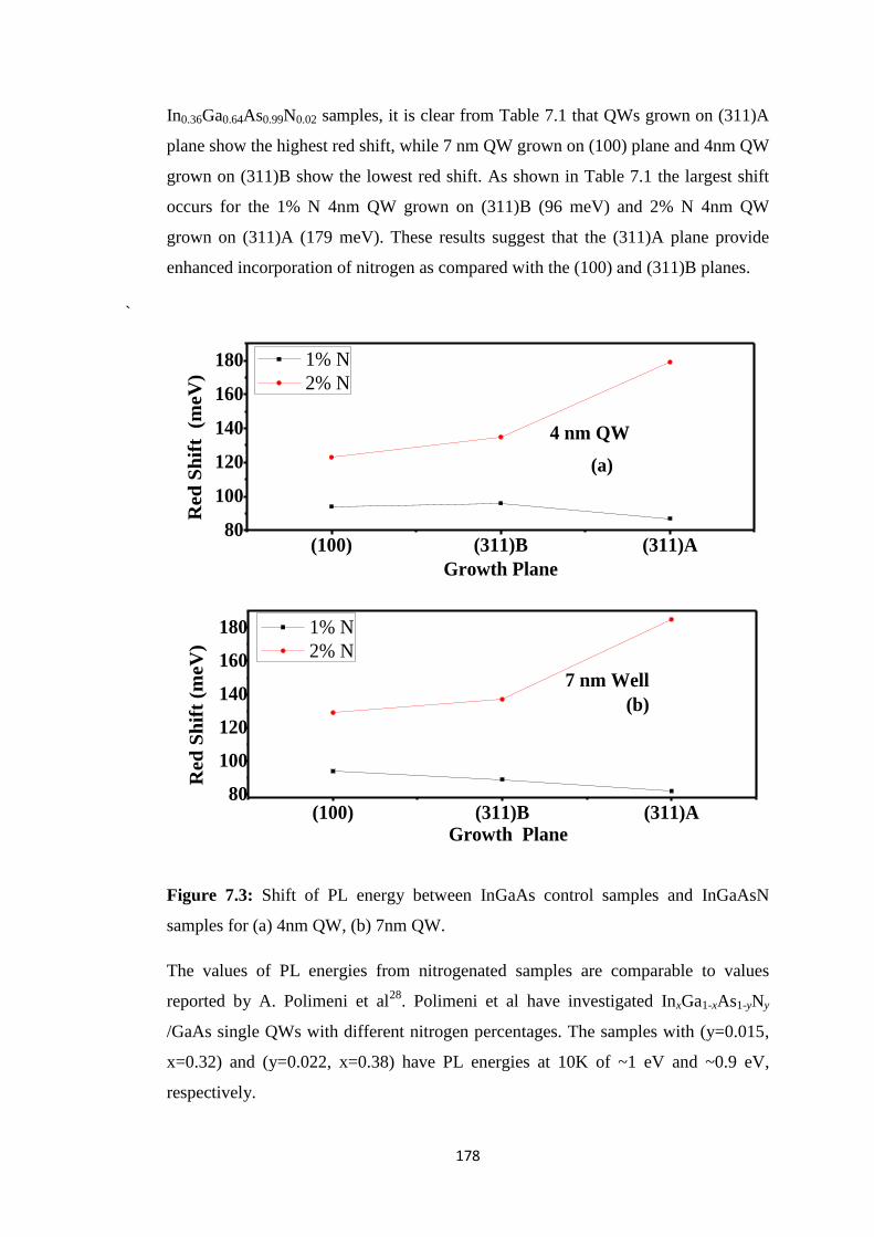
178
In0.36Ga0.64As0.99N0.02 samples, it is clear from Table 7.1 that QWs grown on (311)A
plane show the highest red shift, while 7 nm QW grown on (100) plane and 4nm QW
grown on (311)B show the lowest red shift. As shown in Table 7.1 the largest shift
occurs for the 1% N 4nm QW grown on (311)B (96 meV) and 2% N 4nm QW
grown on (311)A (179 meV). These results suggest that the (311)A plane provide
enhanced incorporation of nitrogen as compared with the (100) dna (311)B planes.
`
Figure 7.3: Shift of PL energy between InGaAs control samples and InGaAsN
samples for (a) 4nm QW, (b) 7nm QW.
The values of PL energies from nitrogenated samples are comparable to values
reported by A. Polimeni et al28
. Polimeni et al have investigated InxGa1-xAs1-yNy
/GaAs single QWs with different nitrogen percentages. The samples with (y=0.015,
x=0.32) and (y=0.022, x=0.38) have PL energies at 10K of ~1 eV and ~0.9 eV,
respectively.
(100) (311)B (311)A80
100
120
140
160
180
Red
Sh
ift
(m
eV
)
Growth Plane
1% N
2% N
4 nm QW
(a)
(100) (311)B (311)A80
100
120
140
160
180
Red
Sh
ift
(meV
)
Growth Plane
1% N
2% N
7 nm Well
(b)

179
This difference in N incorporation in QWs grown on different substrate orientations
could be explained in light of atomic bonding geometries since the nitrogen atom
replace the As atoms. The (n11)B surfaces consists of (100) terraces and (111) steps.
The As atoms on the B steps are bonded with triple dangling bonds from Ga atoms,
indicating that As atoms are difficult to be replaced by N atoms. On the other hand
the (n11)A surface consists of (100) terraces and A-type steps. The As atoms on the
A-type steps are bonded with single dangling bonds from the Ga atoms while those
on the (100) terraces are bonded with double dangling bonds18
. Figure 7.4 shows the
atomic arrangement of the (n11)A and (n11)B surfaces.
Figure 7.4: Atomic arrangements of the (n11)A and (n11)B surfaces18
.
Although the incorporation of nitrogen narrows the bandgap of InGaAs, it affects the
PL intensity drastically. In this work the PL intensity decreases for all substrates with
increasing nitrogen concentration. In fact the PL intensity quenches after
incorporation of 2% N by nearly two order of magnitude, 50 times, and 30 times for
QWs grown on (100), (311)B, and (311)A, respectively.

180
Polimeni et al28
showed that the PL intensity is quenched by a factor of 7 and 130
upon increasing the nitrogen incorporation to 1.5% and 2.2%, respectively.
Earlier studies have pointed out that the incorporation of nitrogen into InGaAs
increases the density of defects originating from compositional and structural
inhomogeneities, and deteriorates the crystalline quality29
.
A correlation between the PL line width and nitrogen concentration is shown in
Figure 7.5. The PL line width broadens with the increase of N incorporation. PL
from nitrogenated QWs grown on (311)B show the highest FWHM among all
planes.
Figure 7.5: Effect of nitrogen incorporation on the FWHM for the three different
growth planes (a) 4nm QW, (b) 7 nm QW.
The FWHM broadening phenomenon, which indicates an increase of the degree of
compositional and structural disorder, is common in quaternary GaInAsN alloys and
has been reported by several groups. M. Pinault and E. Tournie25
showed that the
FWHM increases from 12 meV for a GaInAs QW to 33 meV for a GaInAs0.975N0.025
QW, while S. Shirakata et al30
observed that the FWHM increased from 9 meV for
GaInAs QW to 16.5 meV for GaInAs0.99N0.01 QW. The lowest FWHM recorded for
GaInAsN is 11 meV at 10K for samples grown by S. Shirakata et al31
with 1%
nitrogen.
0% N 1% N 2% N
15
20
25
30
35
40
FW
HM
(m
eV
)
Nitrogen Percentage
(100)
(311)A
(311)B
7 nm QW
(b)
0% N 1% N 2% N10
15
20
25
30
35
40
FW
HM
(m
eV
)
Nitrogen Percentage
(100)
(311)A
(311)B
4 nm QW
(a)

181
7.3.2 CORRELATION BETWEEN TRANSMISSION ELECTRON
MICROSCOPY IMAGES AND FULL WIDTH AT HALF MAXIMUM OF PL
SPECTA OF In0.36Ga0.64As0.99N0.01/GaAs DOUBLE QUANTUM WELLS.
It is well known that there is a direct correlation between structural and optical
properties of QWs, and therefore cross-section transmission electron microscopy
(TEM) was used in order to compare the structural properties of the (100), (311)A
and (311)B QWs.
The FWHM of the PL spectra is a very important parameter that gives an indication
of the quality of the samples and uniformity of epitaxial growth.
Figure 7.6 illustrates the dependence of the FWHM on the growth plane for different
samples. It is found that the FWHM of the PL spectra of the QWs grown on (311)B
GaAs plane is the highest among all different QWs.
(100) (311)A (311)B
20
24
28
32
36
FW
HM
(m
eV
)
Growth Plane
4nm Well
7nm Well
Figure 7.6: Dependence of FWHM of 4 nm and 7nm QWs with the substrate
orientation.
The largest FWHM of the PL signal obtained from (311)B could be explained by
the low interfacial and crystalline quality as can be seen from TEM images in Figure
7.7 for QWs grown on (100), (311)B and (311)A.
182
From the TEM images, the thicknesses of the two QWs (4nm and 7nm) grown on
(311)A and (100) substrate are very uniform, and the interfaces are very flat as
compared to those of the (533)B samples. (533)B QWs samples show some
thickness variations and a lateral period of undulation. Undulations ("ripples") of the
(533) B interfaces could be associated with the beginning of the growth. However, it
doesn't seem that there is some thickness variation associated with this long-range
undulation.
To further investigate the origin of different PL spectrum of QWs grown on different
planes High Angle Annular Dark Field (HAADF) and energy dispersive X-ray
(EDX) characterization were performed on different DQW samples. The EDX
results of the indium composition measurement in different planes shows similar
ratio of 20%, and 15% for 4nm and 7nm QW, respectively. The distribution of In
inside both thin and thick wells over all planes (Figure 7.8) shows similar profile.
However the HAADF images of the (311)B DQWs shows variation of contrast
observed inside the wells compared to other planes and this is linked to the
inhomogeneity of the indium distribution in this plane (see figure 7.9) The
inhomogeneity of In distribution inside (311)B QW could accounts for the lower PL
efficiency and higher FWHM of quantum wells grown on this plane.

183
Figure 7.7: TEM cross sectional images of In0.36Ga0.64As0.99N0.01/GaAs (a) double
QWs grown on (100) plane, (b) 7nm thick QW grown on (100) plane; (c) double
QWs grown on (311)A plane, (d) 7nm thick QW grown on (311)A plane, (e) double
QWs grown on (311) B plane, (f) 7nm thick QW grown on (311)B plane.
(a)
(c) (d)
(e) (f)
(b)
(100) (100)
(311)A (311)A
(311)B (311)B
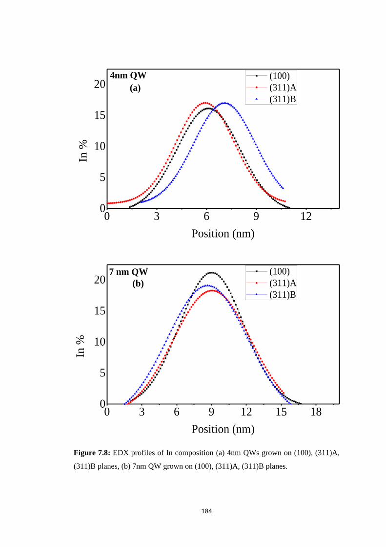
184
Figure 7.8: EDX profiles of In composition (a) 4nm QWs grown on (100), (311)A,
(311)B planes, (b) 7nm QW grown on (100), (311)A, (311)B planes.
0 3 6 9 12 15 180
5
10
15
20 (b)
7 nm QW
In %
Position (nm)
(100)
(311)A
(311)B
0 3 6 9 120
5
10
15
20 (a)
4nm QWIn
%
Position (nm)
(100)
(311)A
(311)B

185
Figure 7.9: HAADF of 7nm In0.36Ga0.64As0.99N0.01/GaAs QW grown on (a) (100)
plane, (b) (311)A plane, (c) (311)B plane.
(a) (b)
(c)
(100) (311)A
(311)B

186
7.3.3 TEMPERATURE DEPENDENCE OF PHOTOLUMINESCENCE: A
COMPARISON AMONG In0.36Ga0.64As1-yNy/GaAs DOUBLE QWs GROWN
ON DIFFERENT SUBSTRATES WITH DIFFERENT NITROGEN
PERCENTAGE.
7.3.3.1 INTRODUCTION AND LITERATURE REVIEW OF
TEMPERATURE DEPENDENCE OF PL FOR InGaAs1-yNy/GaAs QWs.
The PL energy of most crystalline semiconductors decreases monotonically as a
function of temperature, following the conventional Varshni‟s formula. However, the
PL energy of GaAsN or GaInAsN usually shows an anomalous temperature
dependence behavior. The PL energy versus temperature plot shows red- blue - red
shift as the temperature increases. This behavior, referred to as S-shape, is attributed
to exciton localization effect due to local fluctuation of nitrogen concentration32
.
L. Grenouillet et al33
reported an anomalous temperature dependence of the PL
spectrum of a 7 nm Ga0.72In0.28N0.028As0.972 /GaAs single QW. The PL peak energy
exhibited an inverted S-shape dependence with temperature. Below 100K, the PL
integrated intensity showed temperature dependence similar to that of amorphous
semiconductors. The observed anomalous behavior is explained by a strong
localization of carriers at low temperatures that could be induced by the presence of
nitrogen.
F. Laia et al29
studied the temperature dependence of optical properties of
InGaAsN/GaAs single QWs grown by MBE with N contents varying from 0% to
5.3% by PL. The evolution of the peak positions of InGaAs/GaAs samples were in
agreement with the empirical Varshni model. However, pronounced temperature-
dependent S-shaped peak positions were observed in PL spectra while increasing
nitrogen concentration.
M. Pinault et al34
have compared the PL-Temperature dependent properties of
relatively high N-content (~0.04– 0.05) GaInAsN QWs with those of GaAsN and
GaInAs QWs. Strong carrier localization is observed only in GaInAsN QWs with
localization and delocalization temperatures at around 50K and 150 K, respectively.

187
The localization is stronger in the less PL efficient GaInAsN QWs. Their results
demonstrate that the simultaneous presence of both In and N, and not solely of N, is
responsible for carrier localization.
7.3.3.2 EXPERIMENTAL RESULTS
The temperature dependence of the PL spectra of In0.36Ga0.64As1-yNy/GaAs double
QWs samples grown on different substrate orientations was also investigated in
order to understand the effect of the nitrogen incorporation on their optical
properties. The excitation energy was 2.62 eV (473 nm) and the excitation power
was kept at 40mW.
In this section, the PL spectra of In0.36Ga0.64As1-yNy/GaAs double QWs samples
grown on different substrate orientations are recorded at different temperatures in
order to gain some insight on the influence of the substrate orientation on the change
of the mechanism of recombination due to nitrogen incorporation. The data is
illustrated in Figures 7.10, 7.11, and 7.12 for (100), (311)A, (311)B, respectively.
The PL emission from the control GaInAs/GaAs QWs samples is characterized by a
symmetric and Gaussian-like shape. However, the emission from dilute nitride
samples is characterized by asymmetric peaks with a low energy tail, which is more
prominent in (311)B QWs. These tail states might originate from recombination of
localized excitons trapped in potential fluctuations due to local fluctuations in
nitrogen concentration.
A typical broad and non-symmetric PL spectrum is usually observed in GaAsInAs
alloys due to recombination of photo-generated carriers trapped by fluctuating
potential (localized states) induced by non-uniform insertion of the nitrogen atoms
into GaAs crystal.
The mechanism responsible for the carrier localization observed in InGaAsN QWs is
still under debate. However, this could be due to the possible occurrence of
composition modulations and/or strong QW width fluctuations in InGaAsN QWs
samples35,36
.

188
Figure 7.10: Temperature dependent PL of GaInAs1-yNy/GaAs DQWs grown on
(100) GaAs plane: (a) y=0, (b) y=0.01, (c) y=0.02.
0.95 1.00 1.05 1.10 1.15 1.20 1.25
InGaAs0.99
N0.01
/GaAs (100)
double QWs
PL
(a.
u)
Energy (eV)
290k
250k
200k
150k
100k
50k
10k
(b)
1.05 1.10 1.15 1.20 1.25
InGaAs/GaAs (100)
double QWs
PL
(a.u
)
Energy (eV)
290K
250K
200K
150K
100K
50K
10K
(a)
0.95 1.00 1.05 1.10 1.15 1.20 1.25
InGaAs0.98
N0.02
/GaAs (100)
double QWs
PL
(a.u
)
Energy (eV)
290k
250k
200k
150k
100k
50k
30k
10k
(c)

189
Figure 7.11: Temperature dependent PL of GaInAs1-yNy/GaAs DQWs grown on
(311)A GaAs plane: (a) y=0, (b) y=0.01, (c) y=0.02.
1.10 1.15 1.20 1.25
InGaAs/GaAs (311)A
double QWs
PL
(a.u
)
Energy (eV)
290K
250K
200K
150K
100K
50K
10K
(a)
1.00 1.05 1.10 1.15 1.20 1.25
InGaAs0.99
N0.01
/GaAs (311)A
double QWs
PL
(a.u
)
Energy (eV)
290K
250K
200K
150K
100k
50k
10k
(b)
0.90 0.95 1.00 1.05 1.10
InGaAs0.98
N0.02
/GaAs (311)A
double QWs
PL
(a.u
)
Energy (eV)
290K
250K
200K
150K
100K
50K
10K
(c)

190
Figure 7.12: Temperature dependent PL of GaInAs1-yNy/GaAs DQWs grown on
(311)B GaAs plane: (a) y=0, (b) y=0.01, (c) y=0.02.
0.95 1.00 1.05 1.10 1.15 1.20 1.25
InGaAs0.99
N0.02
/GaAs (311)B
double QWs
PL
(a.
u)
Energy (eV)
290K
250k
150k
100k
50k
10K
(c)
1.05 1.10 1.15 1.20 1.25
InGaAs/GaAs (311)B
double QWs
PL
(a.
u)
Energy (eV)
280K
250K
200K
150K
100K
50K
10K
(a)
0.95 1.00 1.05 1.10 1.15 1.20
InGaAs0.99
N0.01
/GaAs (311)B
double QWs
PL
(a.
u)
Energy (eV)
290k
250k
200K
150k
120k
80k
50k
30K
10k
(b)

191
The PL energy of the 4 and 7 nm QWs at 10 K and 290 K for all planes are presented
in Table 7. 2. A striking point in PL data is the fact that the redshift (ΔE) between 10
K and 492 K of the PL peak energy is noticeably lower for (311)B nitrogenated
double QWs than (311)B control GaInAs/GaAs double QWs.
Table 7.2: PL energy of 4 and 7 nm In0.36Ga0.64As1-yNy/GaAs QWs at 10K and
290K.
Growth Plane (100) (311) A (311) B
QW Thickness 4nm 7nm 4nm 7nm 4nm 7nm
10K PL energy of GaInAs
(eV)
1.222 1.16 1.236 1.165 1.233 1.165
290K PL energy of GaInAs
(eV)
1.153 1.089 1.165 1.093 1.157 1.085
ΔE for GaInAs QW (meV) 70 74 73 75 76 80
10K PL energy of
In0.36Ga0.64As0.99N0.01 (eV)
1.128 1.066 1.149 1.083 1.137
1.076
290K PL energy of
In0.36Ga0.64As0.99N0.01 (eV)
1.067 1.004 1.092 1.022 1.098
1.024
ΔE for In0.36Ga0.64As0.99N0.01
QW (meV)
62 68 57 61 39 55
10K PL energy of
In0.36Ga0.64As0.98N0.02 (eV)
1.099 1.043 1.057 0.989 1.132 1.028
290K PL energy of
In0.36Ga0.64As0.98N0.02 (eV)
1.041 0.979 0.993
0.928
1.095
0.978
ΔE for In0.36Ga0.64As0.98N0.02
QW (meV)
60 63 63 60 36 49.9
The PL peak energy of the 4 and 7 nm GaInAs/GaAs QWs on all planes shows a
monotonic decrease with increasing temperatures following the Varshni relation.

192
The temperature dependence of the peak energy is depicted in Figure 7.13 (a,b,c) for
GaInAs grown on (100), (311)A, and (311)B, respectively. The red solid line
represents the fitting results using the empirical Varshni model37
.
2
( ) (0)T
E T ET
Where E(0) is the band gap energy at zero Kelvin, α and β are empirical parameters
related to the material. The optimum fitting parameters, α and β, are given in Table
7.3 for all orientations. Reported values for the (100) are also added at the end of the
table for comparison purposes.
Figure 7.13: Evolution of PL peak energies as a function of temperature for 4 and
7nm GaInAs QWs grown on (a) (100) plane, (b) (311)A plane, and (c) (311)B plane.
The solid red lines are fitting curves using the empirical Varshni model.
0 50 100 150 200 250 3001.08
1.12
1.16
1.20
1.24
1.28
1.32
En
ergy
(eV
)
Temperature (K)
GaInAs_4nm
GaInAs_7nm
Varshni fit
(100) (a)
0 50 100 150 200 250 3001.08
1.12
1.16
1.20
1.24
1.28
1.32
En
ergy
(eV
)
Temperature (K)
GaInAs_4nm
GaInAs_7nm
Varshni Fit
(311)A (b)
0 50 100 150 200 250 3001.08
1.12
1.16
1.20
1.24
1.28
1.32
En
erg
y (
eV
)
Temperature (K)
GaInAs_4nm
GaInAs_7nm
Varshni fit
(311)B (c)

193
Table 7.3: Fitting parameters of Varshni empirical formula for 4 and 7nm GaInAs
double QWs grown on different substrate orientations.
QW Thickness (Plane) E0 (eV) α (10-4
meV/K) β (K)
4 nm (100) QW 1.223 5.67 401
4 nm (311)A QW 1.235 4.8 293
4 nm (311)B QW 1.235 3.71 105
7 nm (100) QW 1.161 5.24 327
7 nm (311)A QW 1.163 5.61 379
7 nm (311)B QW 1.165 4.53 174
(100) GaInAs (Reference 29) 1.187 5.8 310
(100) GaInAs (Reference 34) 1.271 6 350
9 nm (100) GaInAs (Reference 38) 1.232 6.8 480
The dependence of PL peak energy on temperature for InGaAs1-yNy/GaAs samples is
plotted in Figure 7.14, and Figure 7.15 for samples with N=0.01, and 0.02
respectively. Obviously, the band gap evolution as a function of temperature of
(311)B QWs does not follow the behavior of a semiconductor band gap predicted by
Varshni‟s formula. The solid lines represent the fitting results using empirical
Varshni‟s model. The fitting for (311)B samples is done only in the high temperature
range (100-300)K.
The PL peak energy of (311)B InGaAs1-yNy/GaAs QWs in (10-100)K temperature
region exhibits a successive red-blue-red shift as shown in the plot of PL peak
energy versus temperature.
The departure of the temperature dependence of the PL peak energy from its usual
monotonic behaviour as described by Varshni‟s formula due to the regular carriers
thermalization provides strong evidence that the carriers at low temperatures (<~100
K) are localized. With increasing the temperature, the PL peak energy decreases
monotonically with temperature. This unusual behaviour of PL energy with
temperature is commonly attributed to the localized behavior of the excitons due to
the N-induced potential fluctuations.

194
Band tail states in the density of states39
originating from the defects introduced by
nitrogen is responsible for this unusual temperature dependence shape of emission
energy, which only appears for (311)B QWs. At low temperatures, the excitons are
localized in the band-tails in the density of states. The exciton localization in the III-
V-N alloys is caused by potential fluctuations at the band edges due to the
perturbations of the conduction band induced by local fluctuation in nitrogen
concentration (i.e non uniform nitrogen insertion). This behavior has been discussed
previously in section 2.8.3 which dealt with the properties of dilute nitride alloys.
As the temperature is increased, the excitons gain sufficient thermal energy to
overcome small potential barriers and become trapped in the adjacent lower-energy
states where they recombine with reduced emission energies (red-shift). As the
temperature increases further to a Ttrans value (~30 K), excitons start to gain
sufficient thermal energy and the occurrence of a blueshift is observed due to the
transfer of thermally activated excitons from lower- to higher-energy band-tail states.
At Tdeloc the excitons have become almost delocalized and from then on the emission
energy as a function of temperature follows a Varshni-like shape.
Ttrans and Tdeloc are defined as the temperature at which localized excitons begin to
transfer to higher energy localized states and the temperature at which delocalization
of the carriers is complete, respectively.
The carrier localization energy at any temperature is given by the difference Eloc(T) =
E(T) - EPL(T). The localisation energies at 10 K are given in Figures 7.16, and 7.15
for samples with N=0.01, and 0.02 respectively. A superposition of the Varshni fit
and experimental data for (100) and (311)A DQWs indicates that the carriers are
fully delocalized. The localization energies at 10 K and the values of Ttrans and Tdeloc
are reported in Table 7.4.
The PL peak energies of (311)B InGaAs1-yNy/GaAs QWs show a successive
red/blue/redshift in the temperature range 10-290 K. The PL peak energies in the
temperature ranges 10-30K, 30-100K, and >100K redshift, blueshift, and redshift,
respectively. This anomalous behaviour is known as the „„S shape‟‟. This behaviour
has been observed in InGaN40
and AlGaN41
bulk materials, and in QW
heterostructures such as GaAs/InGaP42
, CdS/ZnSe43
and InGaNAs/GaAs33,44
. This S-
behaviour is absent in the (100) and (311)A InGaAsN QW samples investigated in

195
this thesis. The PL peak energies of nitrogenated QWs grown on (100) and (311)A
planes show a usual behaviour of monotonic decrease with temperature.
H. Dumont et al32
compared the optical properties of GaAs1-yNy/GaAs epilayers and
QW structures grown by MOVPE. A difference in the temperature behavior of the
PL peak energy between the GaAsN epilayer and QWs was observed. H. Dumont et
al showed that the PL emission at low temperature from GaInAs QWs results from
direct gap transition with band to band origin. Electron–holes confinement energy in
the QWs that leads to radiative recombination becomes stronger than the exciton
localization energy (i.e confinement of carriers can screen the local potential
fluctuation due to nitrogen atoms). An S-shape dependence of the peak energy
versus temperature for the GaAsN epilayer was reported. A localization effect due to
the non-uniform insertion of nitrogen is stronger in epilayer samples. The “S-shape”
behavior which is attributed to exciton localization effect is due to local fluctuation
of nitrogen concentration32
or QW width fluctuations. These could be absent in QWs
grown on (100) and (311)A due to good uniformity of QW/barrier interface as
demonstrated by TEM images in contrast to (311)B QW/barrier interface that shows
undulations. The absence of this well-known S-behavior in (100) and (311)A QWs
could be as well due to the low nitrogen concentration of 1% and 2%.

196
Table 7.4: Varshni‟s parameters for the temperature dependence of the PL peak
energy for DQWs grown on different substrate orientations with different N
concentrations.
QW
Thickness
(Plane)
E0
(eV)
α
( meV
/ K )
β
(K)
Eloc
(10 K)
(meV)
Ttrans
(K)
Tdeloc
(K)
4nm (311)B
QW (1%N)
1.166 0.37 163 65 72 100
7nm (311)B
QW (1%N)
1.098 0.458 200 35 60 100
7nm (311)B
QW (2%N)
1.15 0.98 1142 37 60 100
7nm (311)B
QW (2%N)
1.046 0.37 180 30 40 80
4nm (100)
QW (1%N)
1.13 1.41 1619 ------- -------- -------
7nm (100)
QW(1%N)
1.066 0.711 635 ------- -------- -------
4nm (100)
QW(2%N)
1.102 2.5 3105 ------- -------- -------
7nm (100)
QW (2%N)
1.099 1.78 2029 ------- -------- -------
4nm (311)A
QW (1%N)
1.15 0.275 120 ------- -------- -------
7nm (311)A
QW(1%N)
1.082 0.416 291 ------- -------- -------
4nm (311)A
QW (2%N)
1.056 0.32 178 ------- -------- -------
7nm (311)A
QW(2%N)
0.99 0.28 117 ------- -------- -------

197
Figure 7.14: Evolution of the temperature of the PL peak energies of the
GaInAs0.99N0.01/GaAs QWs grown on (100), (311)A, (311)B GaAs planes; (a)
QW=4nm (N=0.01); (b) QW=7nm (N =0.01).
0 50 100 150 200 250 300
1.06
1.08
1.10
1.12
1.14
1.16
1.18
N=0.01
4 nm QW
Tdeloc
Ttrans
E loc(10K) =43 meV
En
erg
y (
eV
)
4 nm QW
Temperature (K)
(100)
(311)A
(311)B
Fit of (100)
Fit of (311)A
Fit of (311)B
(a)
0 50 100 150 200 250 300
1.00
1.02
1.04
1.06
1.08
1.10
1.12
N=0.01Tdeloc
Ttrans
E loc(10K) =35 meV
En
erg
y (
eV
)
Temperature (K)
(100)
(311)A
(311)B
varshni Fit of (100)
varshni Fit of (311)A
varshni Fit of (311)B
7 nm QW (b)

198
Figure 7.15: Evolution of the temperature of the PL peak energies of the
GaInAs0.98N0.02/GaAs QWs grown on (100), (311)A, (311)B GaAs planes (a)
QW=4nm (N=0.02); (b) QW=7nm (N=0.02).
0 50 100 150 200 250 3000.98
1.00
1.02
1.04
1.06
1.08
1.10
1.12
1.14
1.16
1.18
N=0.02
Ttrans
Tdeloc
En
ergy
(eV
)
Temperature (K)
(100)
(311)A
(311)B
Fit of (100)
Fit of (311)A
Fit of (311)B
4 nm QW
(a)
E loc(10K) =37 meV
0 50 100 150 200 250 3000.92
0.94
0.96
0.98
1.00
1.02
1.04
1.06
N=0.027 nm QW
Tdeloc
E loc(10K) =30 meV
En
ergy
(eV
)
Temperature (K)
(100)
(311)A
(311)B
Fit of (100)
Fit of (311)A
Fit of (311)B
7 nm QW
(b)
Ttrans

199
7.4 CONCLUSION
The influence of nitrogen content on the optical properties of InGaAsN/ DQWs
grown on different GaAs crystal orientations has been studied by photoluminescence
(PL), Transmission Electron Microscopy (TEM), High Angle Annular Dark Field
(HAADF) and Energy Dispersive X-ray (EDX).
The PL efficiency was found to decrease with increasing nitrogen content for all
planes but with different order of magnitudes. This phenomenon suggests that the
nitrogen incorporation creates defect-related nonradiative centers, whose
concentrations are plane dependent.
An enhanced N incorporation is observed in (311)A GaInAsN QWs as compared
with (311)B and (100) samples.
The peak PL energies of InGaAs/GaAs and InGaAsN/GaAs DQWs grown on the
different planes follow the empirical Varshni model, except for the (311)B
InGaAsN/GaAs DQWs where a pronounced S-shaped behavior was observed. These
latter results demonstrate that the nitrogen incorporation into the (311)B plane has
strong influence on carrier localization. Cross-sectional TEM images show that the
(311)B QWs are undulated, which may account for this potential fluctuation and
carrier localization.

200
REFRENCES
1 M. Weyers, M. Sato, and H. Ando, Japanese Journal of Applied Physics, 31, L853
(1992).
2 Semicond. Sci. Technol. 17(8) (2002), special issue on dilute nitrides, Journal of
Physics: Condensed Matter, 16(31) (2004).
3 D. Friedman, and S. Kurtz, Progress in Photovoltaics Research and Application, 10,
331 (2002).
4 T. Jouhti, O. Okhotnikov, J. Konttinen, L. Gomes, C. Peng, S. Karirinne, E.
Pavelescu, and M. Pessa, New Journal of Physics, 5, 84.1 (2003).
5 K. Choquette, J. Klem, A. Fischer, O. Blum, A. Allerman, I. Fritz, S. Kurtz, W.
Breiland, R. Sieg, K. Geib, J. Scott, and R. Naone, Electronics Letters, 36, 1388
(2000).
6 G. Steinle, A. Egorov, and H. Riechert, Electronics Letters, 37, 93 (2001).
7 T. Kitatani, K. Nakahara, M. Kondow, K. Uomi, and T. Tanaka, Japanese Journal
of Applied Physics, 39, L86 (2000).
8 M. Kondow, K. Uomi, A. Niwa, T. Kitatani, S. Watahiki, and Y. Yazawa,
Japanese Journal of Applied Physics, 35, 1273 (1996).
9 M. Kondow, T. Kitatani, K. Nakahara, and K. Uomi, Lasers and Electro-Optics
Society Annual Meeting, LEOS '98 IEEE (1998).
10 H. Xina, and C. Tu, Applied Physics Letters, 72, 2442 (1998).
11 J. Phillipsin, A. Alper, J. Margrave, and A. Nowick, Eds. Bonds and Bands in
Semiconductors, Academic Press, New York, 54 (1973).

201
12
H. Ho, and G. Stringfellow, Materials Research Society Symposia Proceedings,
449, 871 (1997).
13 B. Lee, S. Bose, M. Kim, A. Reed, G. Stillman, W. Wang, L. Vina, and P. Colter
Journal of Crystal Growth, 96, 27 (1989).
14 X. Han, T. Tanak, N. Kojima, Y. Ohshita, M.Yamaguchi, and S.Sato, Applied
Physics Letters, 100, 032108 (2012).
15 H. Suzuki, M. Inagaki, T. Honda, Y. Ohshita, N. Kojima, and M. Yamaguchi,
Japanese Journal of Applied Physics, 49, 04DP08 (2010).
16 A. Moto, M. Takahashi, and S. Takagishi, Japanese Journal of Applied Physics,
39, L1267 (2000).
17 M. Takahashi, P. Vaccaro, T. Watanabe, T. Mukaihara, F. Koyama, and K. Iga,
Japanese Journal of Applied Physics, 35, 6102 (1996).
18 H. Saito, T. Makimoto, and N. Kobayashi, Japanese Journal of Applied Physics,
Part 2, 35, L1644 (1996).
19 J. Ibanez, M. Henini, R. Kudrawiec, J. Misiewicz, M. Schmidbauer, and M.
Hopkinson, Journal of Crystal Growth, 552, 301 (2007).
20 X. Han, H. Suzuki, J. Lee, M. Inagaki, N. Kojima, Y. Ohshita, and M. Yamaguchi,
Proc. 35th IEEE Photovoltaic Specialist Conference Honolulu, HI, 20, (2010).
21 A. Arnoult, F. Gonzalez-Posada, S. Blanc, V. Bardinal, and C. Fontaine, Physica
E, 23, 352 (2004).
22 S. Blanc, A. Arnoult, H. Carrere, and C. Fontaine, Physica E, 17, 252 (2003).

202
23
S. Blanc, A. Arnoult, H. Carrère, E. Bedel, G. Lacoste, C. Fontaine, M. Cabié, A.
Ponchet, and A. Rocher, IEE Proc-Optoelectron., 150, 64 (2003).
24 T. Ishizuka, H. Doi, T. Katsuyama, J. Hashimoto, and M. Nakayama, Journal of
Crystal Growth, 298, 116 (2007).
25 M. A Pinault, and E. Tournie, Applied Physics Letters, 79 (21), 3404 (2001).
26 C. Chana, J. Wub, Y. Huangb, H. Hsuc, K. Tiongd, and Y. Sue, Materials
Chemistry and Physics, 124, 1126 (2010).
27 N. Nishiyama, M. Arai, S. Shinada, T. Miyamoto, F. Koyama, and K. Iga, Journal
of Crystal Growth, 221, 530 (2000).
28 A. Polimeni, M. Capizzi, M. Geddo, M. Fischer, M. Reinhardt, and A. Forchel,
Applied Physics Letters, 77, 2870 (2000).
29 F. Laia, S. Kuo, J.S. Wangc, R. Hsiao, H. Kuo, J. Chi, S. Wang, H. Wang, C.
Liang, and Y. Chen, Journal of Crystal Growth, 291, 27 (2006).
30 S. Shirakata, M. Kondow, and T. Kitatani, Applied Physics Letters, 79, 54 (2001).
31 S. Shirakata, M. Kondow, and T. Kitatani, Journal of Physics and Chemistry of
Solids, 64, 1533 (2003).
32 H. Dumont, L. Auvray, Y. Monteil, F. Saidi , F. Hassen, and H. Maaref, Optical
Materials, 24, 303 (2003).
33 L. Grenouillet, C. Bru-Chevallier, G. Guillot, P. Gilet, P. Duvaut, C. Vannuffel, A.
Million, and A. Chenevas-Paule, Applied Physics Letters, 76, 2241 (2000).
34 M. Pinault, and E. Tournié, Applied Physics Letters, 78, 1562 (2001).

203
35
H. Xin, K. Kavanagh, Z. Zhu, and C. Tu, Applied Physics Letters, 74, 2337
(1999).
36 Y. Soo, S. Huang, Y. Kao, J. Chen, S. Hulbert, J. Geisz, S. Kurtz, J. Olson, S.
Kurtz, E. Jones, and A. Allerman, Physical Review B, 60, 13605 (1999).
37 Y. Varshni, Physica (Utrecht), 34, 149 (1967).
38 P. Sitarek, K. Ryczko, G. Sezk, J. Misiewicz, M. Fischer, M. Reinhardt, and A.
Forchel, Solid-State Electronics, 47, 489 (2003).
39 A. Kaschner, T. Luttgert, H. Born, A. Hoffman, A.Yu. Egorov, and H. Riechert,
Applied Physics Letters, 78 (10), 1391 (2001).
40 H. Schenk, M. Leroux, and P. Mierry, Journal of Applied Physics, 88, 1525
(2000).
41 Y. Cho, G. H. Gainer, J. Lam, J. Song, W. Yang, and W. Jhe, Physical Review B,
61, 7203 (2000).
42 E. Laureto, E. Meneses, W. Carvalho, A. Bernussi, E. Ribeiro, E. da Silva, and J.
de Oliveira, Brazilian Journal of Physics., 32, 314 (2002).
43 A. Dinger, M. Baldauf, S. Petillon, A. Hepting, D. Luerssen, M. Grun, H. Kalt,
and C. Klingshirn, Journal of Crystal Growth, 214, 660 (2000).
44 A. Kaschner, T. Luttgert, H. Born, A. Hoffmann, A. Egorov, and H. Riechert,
Applied Physics Letters, 78, 1391 (2001).

204
CHAPTER 8: POST GROWTH ANNEALING OF Ga1-
xInxNyAs1-y/GaAs DOUBLE QUANTUM WELL
STRUCTURES GROWN ON (100), (311)A, and (311)B
GaAs SUBSTRATES

205
This chapter reports the effect of the post-growth annealing process on the optical
properties of Ga1-xInxNyAs1-y/GaAs double quantum well structures grown on (100),
(311)A, and (311)B GaAs substrates.
8.1 INTRODUCTION
The introduction of nitrogen into the GaAs lattice by replacing As atoms creates
localized energy states near the conduction band edge. This leads to a huge band gap
bowing1 that affects the electrical and optical properties of the materials
2. However,
nitrogen also occupies the non-substitutional sites in the lattice of GaAs (i.e. the
nitrogen atoms may incorporate in locations other than the group V lattice sites3)
leading to the formation of N-related defects that can degrade the optical quality of
the crystal by decreasing the optical efficiency and carrier lifetime4,5
. The usage of
radio frequency (RF) plasma source to generate nitrogen atoms and the relative low
growth temperature are also responsible for the creation of these defects and low
optical quality.
In order to recover these qualities it is common practice to subject the material to
appropriate thermal treatment to improve the optical properties of nitrogen-based III-
V compounds6. However, the annealing process can have also a negative effect on
the material quality and the defects present in the host material.
Shafi et al7 used deep level transient spectroscopy (DLTS) and Laplace DLTS
techniques to study the annealing effect on Si-doped GaAsN layers containing
nitrogen concentrations in the range 0.2 – 1.2%. Seven defect states were observed in
the as-grown GaAsN (N=0.2%) samples. Post-growth thermal annealing eliminated
four of these defects. However, in the samples of high nitrogen content ≥ 0.8%, both
creation and annihilation of some of the traps have been observed upon annealing.
Gao et al8 studied the effect of rapid thermal annealing on the evolution of
electrically active defects in metalorganic vapour phase epitaxy (MOCVD) grown p-
type GaAsN epitaxial layers using DLTS. Annealing between 600 0C and 900
0C
generated six new deep hole traps. Most of these were stable in this temperature

206
range. However, there were variations in their concentrations with the annealing
temperature.
S. Spruytte et al3 investigated GaNAs QW by high resolution x-ray diffraction. They
observed that the lattice parameter does decrease linearly with increasing nitrogen
concentration up to 2.9 % as expected by Vegard’s law. By increasing the nitrogen
percentage above this value deviation from Vegard’s low occurred. The fact that
Vegard’s law is not observed for all nitrogen contents indicates that nitrogen
incorporates in locations other than the group V lattice sites. X-ray photoelectron
spectroscopy (XPS) revealed that nitrogen exists in two bonding configurations: a
Ga–N bond and another nitrogen complex in which N is less strongly bonded to
gallium atoms. The authors reported that post growth annealing removes the second
nitrogen complex and improves the PL intensity. A combined nuclear reaction
analysis and Rutherford backscattering technique showed that as-grown GaNAs
contains a significant concentration of interstitial nitrogen that disappears upon
anneal.
Annealing studies of nitride materials reported in the literature have contradictory
results regarding its effect on PL energy. While some reports show a blue shift9 of
the PL emission upon thermal annealing others show a red shift of PL energy10
.
The thermal anneal-induced blue shift is mainly attributed to two distinct
mechanisms; the rearrangement of local nitrogen bonding configurations11
and the
interdiffusion between Ga and In atoms across the QW interfaces12
.
A brief survey about the different effect in PL energy after annealing is given below.
V. Liverini et al13
analyzed several QWs with different nitrogen contents after
different RTA annealing conditions. The main conclusion of their systematic studies
of RTA on GaInNAs single QWs is that the blue shift of the energy band gap after
annealing is dependent on the N content of the QW while the PL integrated intensity
improvement is not. By comparing the effect of the annealing process carried out at
the same conditions on samples with different nitrogen concentration, they found
that the highest blue shift occurs in samples that have the highest N content.
There are two blue shift regimes, namely strong and weak regimes, depending on the
RTA temperature. In the strong regime (up to 700 0C) the blue shift experiences a
rapid increase with increasing RTA temperature, while in the weak regime above

207
this temperature it saturates. By using high resolution x-ray diffraction (HRXRD),
the authors concluded that the larger PL blue shift observed in GaInNAs cannot be
explained just by In out-diffusion.
These findings contradict with the results reported by H. Liua et al12
who showed
suppression of blue shift after annealing in samples with higher nitrogen content. H.
Liua et al used X-ray to study the effect of post-growth annealing on GaInAs/GaAs
and GaInNAs/GaNAs multiple quantum wells (MQWs) grown by MBE. The
evolution of X-ray diffraction patterns indicates that In/Ga inter-diffusion occurs in
both types of MQWs due to post-growth thermal annealing. The diffusion length
deduced from the dynamic simulations shows a decrease with the increase of N
concentration. Alloying nitrogen with GaInAs is interpreted to cause suppression in
Ga/In inter-diffusion. These observations may be attributed to the formation of
strong N-related bonds inside the QW and to a reduced strain in nitrogen-contained
QWs.
8.2 EXPERIMENTAL RESULTS AND ANALYSIS
This section will report on the results of the annealing effect on six samples of Ga1-
xInxNyAs1-y/GaAs double quantum well structures grown on (100), (311)A, and
(311)B GaAs planes with two nitrogen concentration (0% and 1%).
The features of the six studied samples in this section are shown in Table 8.1. All
samples are grown by MBE and are described in details in Chapter 7, section 7.3.
The samples cut from the as-grown wafer were proximity GaAs capped and RTA
treated in argon ambient for 30 s at 500 0C, 600
0C, and 700
0C. The detailed post-
growth annealing procedure is similar to the one adopted to heat treat self-assembled
quantum dots (see Chapter 6, section 2).
It is worth pointing out that GaAs proximity capping technique, which inhibits
surface degradation due to As out diffusion, induces thermal intermixing upon
RTA14
, while SiO215
and Si3N416
capping layers have been reported to enhance
impurity-free interdiffusion. For example the effect of the capping layer (GaAs and
SiO2) on the optical properties of RTA strained InGaAs/GaAs MQWs has been

208
investigated by S. Burkner et al14
. They found that the PL energy shift upon
annealing of SiO2 capped samples resulted up to four times larger than in GaAs
capped samples. This behavior was explained by the quick diffusion of the top most
Ga atoms at the surface into SiO2, creating Ga vacancies which diffuse into the
MQWs region. For the GaAs capped layers, the only available Ga vacancies
contributing to the interdiffusion are the intrinsic Ga vacancies that originate from
the substrate and the buffer layers. This translates to a lower concentration of Ga
vacancies leading to a smaller degree of intermixing in the MQWs region.
To remove the effects of any variations in the annealing process between samples, all
the samples were annealed simultaneously as a batch. PL measurements at 10 K
were performed on each of the samples prior to annealing, and then again following
the annealing process. Further anneals were then performed on the same samples
with the low temperature PL recorded after each anneal.
Table 8.1: Investigated samples grown on different substrate orientations and having
different nitrogen contents.
Sample Number Substrate Nitrogen mole fraction
MBE2226
DQW0.0N
(100)
(100) 0%
MBE2227
DQW0.0N
(311)A
(311)A 0%
MBE2228
DQW0.0N
(311)B
(311)B 0%
MBE2223
DQW0.1N
(100)
(100) 1%
MBE2225
DQW0.01N
(311)A
(311)A 1%
MBE2224
DQW0.01N
(311)B
(311)B 1%

209
8.2.1 PHOTOLUMINESCENCE OF ANNEALED Ga1-xInxAs/GaAs DQWs
SAMPLES AT DIFFERENT TEMPERATURES
Figure 8.1 shows the 10 K PL spectra of as-grown, 500 0C, 600
0C and 700
0C
annealed (100), (311)A, and (311)B Ga1-xInxNyAs1-y/GaAs DQWs samples with
y=0% .
The PL energy of as-grown 4nm QW grown on (100), (311)A, and (311)B samples
are 1.222, 1.266 , and 1.266 eV with FWHM of ~25 , ~13 , ~17 meV, respectively.
While The PL energy of as-grown 7nm QW grown on (100), (311)A, and (311)B
samples are 1.160, 1.165 , and 1.167 eV with FWHM of ~20, ~13, and ~19 meV,
respectively.
It is evident from Figure 8.2 that almost no change of the peak position is observed
when the annealing temperature is 500 0C for QWs grown on (311)A and (311)B
planes, while there is a small red shift of 8 meV, and 12 meV for 4 nm, and 7 nm
(100) QWs, respectively. By increasing the annealing temperature to 600 0C, this red
shift of PL from (100) quantum wells recovered again, while the PL energy of 600
0C annealed (311)A sample red shifted and reaches its lowest value of 1.231 eV, and
1.162 eV for 4 nm and 7 nm wells, respectively. Further increase of the annealing
temperature to 700 0C, the PL energy from QWs grown on all planes exhibit a blue
shift of equal amount of 20 meV for the 4nm QW and of a comparable amount of
10, 15, and 16 for the 7 nm (100), (311)A, and (311)B QW, respectively.
The PL blue-shift at higher annealing temperature is most likely due to Ga and In
inter-diffusion, which seems to be nearly the same for all planes. The inter-diffusion
which results in shallower QW is believed to cause the quantum-confined states to
shift upwards in energy17,18
.
The blueshift of the PL has been explained theoretically19
by a change in the electron
and hole confinement profile due to the annealing-induced interdiffusion of atoms
across the QW interfaces.
The increasing of the PL blue shift with increasing annealing temperature could be
accounted for by the increasing of the diffusion length of atoms at higher annealing
temperature20
.

210
Figure 8.1: 10 K PL spectra of as-grown, and 500 0C, 600
0C and 700
0C annealed
In0.36Ga0.64As/GaAs DQWs samples: (a) (100), (b) (311)A, (c) (311)B. The times
number in front of each spectrum corresponds to the PL relative intensity, referred to
as enhancement factor F=Ipeak (annealed)/Ipeak (as-grown).
1.10 1.15 1.20 1.25 1.30 1.35
x 1
(a)GaInAs/GaAs (100)
PL
(a.u
)
Energy (eV)
700 0C
600 0C
500 0C
As-Grown
x 2.5
x 8
x 13
1.10 1.15 1.20 1.25 1.30 1.35
(b)GaInAs/GaAs (311)A
PL
(a.u
)
Energy (eV)
700 0C
600 0C
500 0C
As-Grown
x1
x1
x1.2
x 4
1.10 1.15 1.20 1.25 1.30 1.35
(c)GaInAs/GaAs (311)B
x9
x3
x1.3
x1
PL
(a.u
)
Energy (eV)
700 0C
600 0C
500 0C
As-Grown
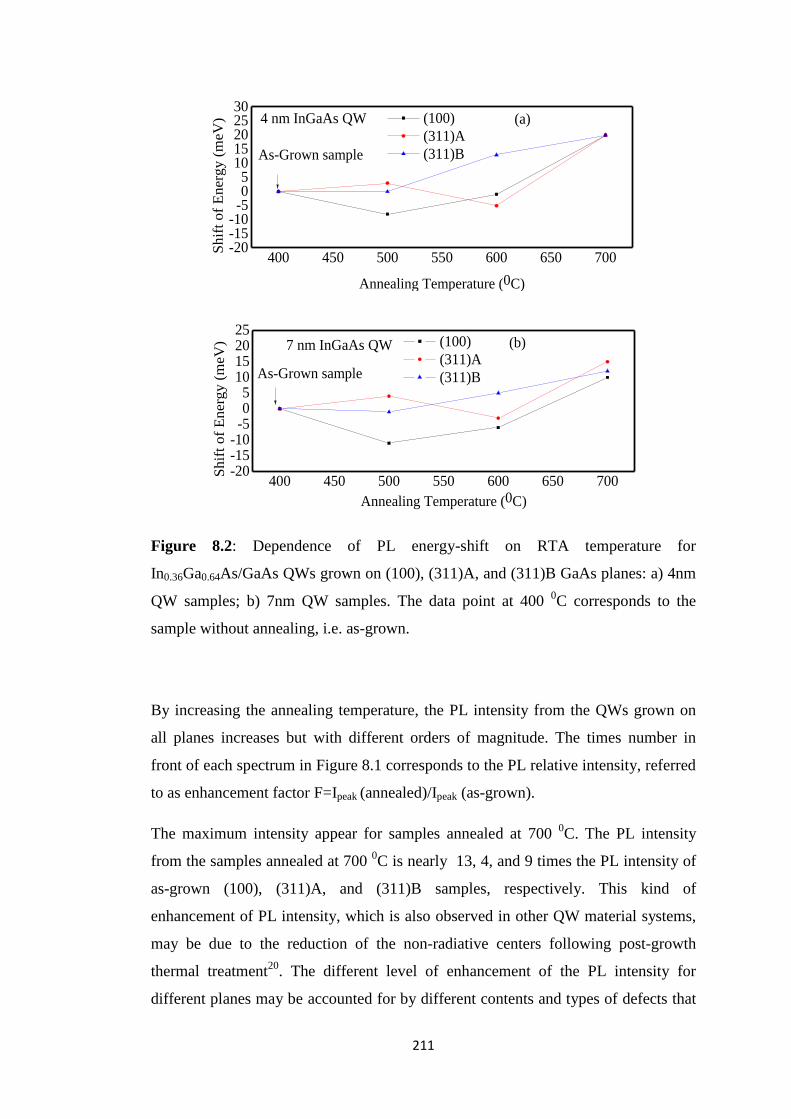
211
Figure 8.2: Dependence of PL energy-shift on RTA temperature for
In0.36Ga0.64As/GaAs QWs grown on (100), (311)A, and (311)B GaAs planes: a) 4nm
QW samples; b) 7nm QW samples. The data point at 400 0C corresponds to the
sample without annealing, i.e. as-grown.
By increasing the annealing temperature, the PL intensity from the QWs grown on
all planes increases but with different orders of magnitude. The times number in
front of each spectrum in Figure 8.1 corresponds to the PL relative intensity, referred
to as enhancement factor F=Ipeak (annealed)/Ipeak (as-grown).
The maximum intensity appear for samples annealed at 700 0C. The PL intensity
from the samples annealed at 700 0C is nearly 13, 4, and 9 times the PL intensity of
as-grown (100), (311)A, and (311)B samples, respectively. This kind of
enhancement of PL intensity, which is also observed in other QW material systems,
may be due to the reduction of the non-radiative centers following post-growth
thermal treatment20
. The different level of enhancement of the PL intensity for
different planes may be accounted for by different contents and types of defects that
400 450 500 550 600 650 700-20-15-10-505
10152025
7 nm InGaAs QW
Sh
ift
of
En
erg
y (
meV
)
Annealing Temperature (0C)
(100)
(311)A
(311)BAs-Grown sample
(b)
400 450 500 550 600 650 700-20-15-10-505
1015202530
As-Grown sample
Sh
ift
of
En
erg
y (
meV
)
Annealing Temperature (0C)
(100)
(311)A
(311)B
4 nm InGaAs QW (a)

212
are present in each plane. The lower PL intensity of the as-grown samples as
compared to the annealed samples could be accounted for by a larger concentration
of nonradiative centers. It could therefore be argued that the PL intensity difference
between as-grown and annealed sample is evidence of lower concentration of
nonradiative centers. As demonstrated by L. H. Li et al20
the increase of the PL
intensity was attributed to the removal of defects and impurities in the well and
heterointerface regions.
M. Albrecht et al21
analyzed the influence of annealing on compositional
fluctuations in InGaAsN quantum wells by means of composition-sensitive high-
resolution transmission electron microscopy (HR-TEM) and PL. They observed an
improvement of the PL intensity after annealing and explained this enhancement by
the homogenization of the In distribution in the QW. In addition, they attributed the
PL shift to homogenization of the In concentration and to diffusion of N out of the
quantum well.
In this work, it is suggested that more detailed analysis, for example by using deep
level transient spectroscopy (DLTS) measurements22
, would be required to show the
nature and evolution of the defects with respect to the growth plane and annealing
temperatures.
The FWHM of PL spectra for annealed samples have different behavior for different
planes. It decreases monotonically for QWs grown on (100) plane while it is constant
for the QWs grown on high index planes. However, FWHM slightly increases for the
4nm QW grown on (311)A after annealing at 700 0C (see Figure 8.3).
The reduction of FWHM of PL of (100) QWs by annealing might be caused by the
improvement of the uniformity of In-content in GaInAs well layer as a result of the
rearrangement and reconstruction at the atomic level brought about by thermal
annealing23
and the reduction of thickness fluctuation of the well20
.
It seems that the annealing temperature has no effect on FWHM of PL from QWs
grown on high index planes. It is important to point out that the as-grown (311)A
QWs have the smallest FWHM among all as-grown samples.
The smallest FWHM of 13 and 11 meV were observed for both 4 nm and 7 nm (100)
QWs annealed at 700 0C, respectively.
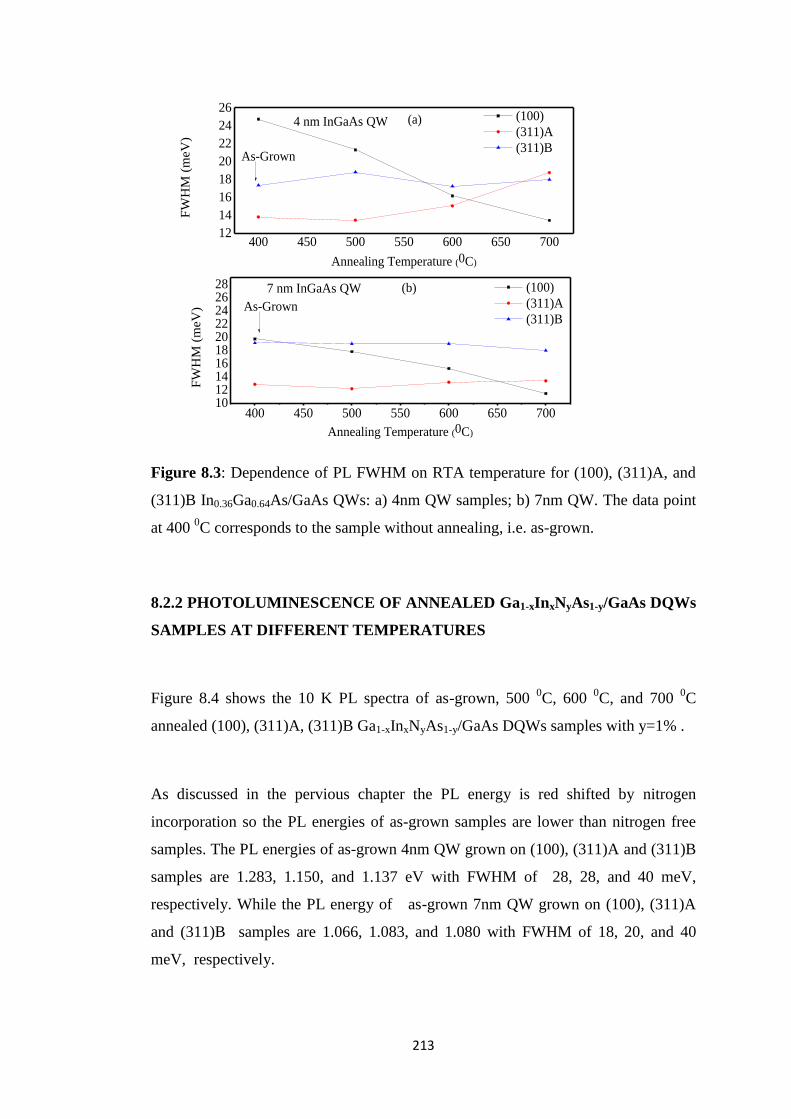
213
Figure 8.3: Dependence of PL FWHM on RTA temperature for (100), (311)A, and
(311)B In0.36Ga0.64As/GaAs QWs: a) 4nm QW samples; b) 7nm QW. The data point
at 400 0C corresponds to the sample without annealing, i.e. as-grown.
8.2.2 PHOTOLUMINESCENCE OF ANNEALED Ga1-xInxNyAs1-y/GaAs DQWs
SAMPLES AT DIFFERENT TEMPERATURES
Figure 8.4 shows the 10 K PL spectra of as-grown, 500 0C, 600
0C, and 700
0C
annealed (100), (311)A, (311)B Ga1-xInxNyAs1-y/GaAs DQWs samples with y=1% .
As discussed in the pervious chapter the PL energy is red shifted by nitrogen
incorporation so the PL energies of as-grown samples are lower than nitrogen free
samples. The PL energies of as-grown 4nm QW grown on (100), (311)A and (311)B
samples are 1.283, 1.150, and 1.137 eV with FWHM of 28, 28, and 40 meV,
respectively. While the PL energy of as-grown 7nm QW grown on (100), (311)A
and (311)B samples are 1.066, 1.083, and 1.080 with FWHM of 18, 20, and 40
meV, respectively.
400 450 500 550 600 650 70012
14
16
18
20
22
24
264 nm InGaAs QW
FW
HM
(m
eV
)
Annealing Temperature (0C)
(100)
(311)A
(311)B
(a)
As-Grown
400 450 500 550 600 650 70010121416182022242628 7 nm InGaAs QW
FW
HM
(m
eV
)
Annealing Temperature (0C)
(100)
(311)A
(311)BAs-Grown
(b)
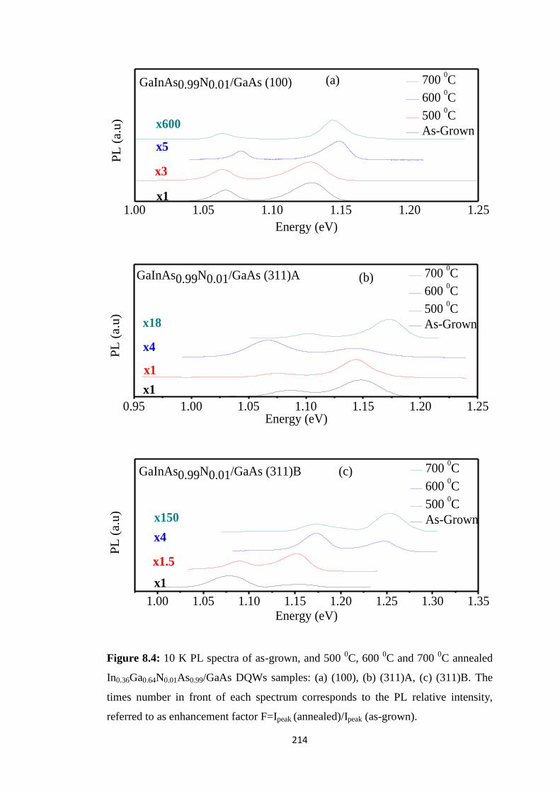
214
Figure 8.4: 10 K PL spectra of as-grown, and 500 0C, 600
0C and 700
0C annealed
In0.36Ga0.64N0.01As0.99/GaAs DQWs samples: (a) (100), (b) (311)A, (c) (311)B. The
times number in front of each spectrum corresponds to the PL relative intensity,
referred to as enhancement factor F=Ipeak (annealed)/Ipeak (as-grown).
1.00 1.05 1.10 1.15 1.20 1.25
GaInAs0.99N0.01/GaAs (100)
x1
x3
PL
(a.u
)
Energy (eV)
700 0C
600 0C
500 0C
As-Grownx600
x5
(a)
0.95 1.00 1.05 1.10 1.15 1.20 1.25
x18
x4
x1
x1
GaInAs0.99N0.01/GaAs (311)A
PL
(a.u
)
Energy (eV)
700 0C
600 0C
500 0C
As-Grown
(b)
1.00 1.05 1.10 1.15 1.20 1.25 1.30 1.35
x150
x4
x1.5
x1
GaInAs0.99N0.01/GaAs (311)B
PL
(a.u
)
Energy (eV)
700 0C
600 0C
500 0C
As-Grown
(c)

215
It is evident from Figure 8.5 that almost no change of the peak position is observed
when the annealing temperature is 500 0C for QWs grown on different planes.
However, by increasing the annealing temperature, the QWs PL energy behaves in a
way that depends on the growth plane. For the QWs grown on (100) plane, the PL
energy shows a blue shift after annealing by an amount comparable (20 meV at 700
0C) to the blue shift observed in the free nitrogen sample (i.e. GaInAs/GaAs). For
QWs grown on (311(B plane, the PL energy show a larger blue shift (120 meV at
700 0C) as compared to 20 meV for free nitrogen sample. On the other hand the
QWs grown on (311)A plane show red shift instead of blue shift that increases with
increasing annealing temperature up to 600 0C; further increase of the annealing
temperature results in a blueshift. For the 700 0C anneal the PL energy shift from
(311)A QWs becomes comparable to that of (100) QWs.
Since the PL energy shifts with annealing for free nitrogen QWs grown on different
planes are comparable, the discrepancy in the shifts of PL energy with annealing
temperature for nitrogenated QWs could be related to nitrogen behavior with
annealing rather than In. This effect could be attributed to a rearrangement of the
nearest neighbour configuration of the N atoms10
.
The red shift in the case of (311)A QWs could be explained by some interstitial
nitrogen atoms that migrated and substituted As atoms.
Francoeur et al.24 reported a redshift in the luminescence peak detected in MOCVD
grown InGaAsN layers after annealing at 650 0C for 5 minutes. A shift of 15 meV in
a sample containing 0.7% N was observed. From the XRD measurement they
attributed this redshift to the increase of nitrogen incorporation.
As shown in Figure 8.4 and indicated by the PL enhancement factor for every
annealing temperature, the annealing process has resulted in an increase of the PL
intensity for all planes. The times numbers inside Figure 8.4 relate to the PL
enhancement factor at each annealing temperature. The magnitude of PL
enhancement factors of nitrogen-containing samples are larger than those of N-free
samples for all planes. The larger increase in the PL intensity of the N-containing
samples would suggest that there is a larger concentration of non-radiative centers
associated with N incorporation. In other words, the traps responsible for the

216
decrease of the luminescence efficiency of the as-grown nitride-samples are related
to a crystal defect or an impurity associated with nitrogen, but not related to indium3.
Figure 8.5: Dependence of PL energy-shift on RTA temperature for (100), (311)A,
and (311)B InGaAs0.99N0.01/GaAs QWs: a) 4nm QW samples b) 7nm QW. The data
point at 400 0C corresponds to the sample without annealing, i.e. as-grown.
400 450 500 550 600 650 700-60
-30
0
30
60
90
120
150
180 7 nm InGaAs0.99
N0.01
QW
Sh
ift
of
En
erg
y (
meV
)
Annealing Temperature (0C)
(100)
(311)A
(311)BAs-Grown sample
(b)
400 450 500 550 600 650 700
0
30
60
90
120
150
180 4 nm InGaAs0.99N0.01 QW
As-Grown sample
Sh
ift
of
En
erg
y (
meV
)
Annealing Temperature (0C)
(100)
(311)A
(311)B
(a)

217
8.3 SIMS OF AS-GROWN and ANNEALED
Ga0.64In0.36N0.1As0.99/GaAs DQWs SAMPLES AT DIFFERENT
TEMPERATURES
In order to elucidate the origin of the PL blue shift, composition profile analysis by
the time of flight secondary ion mass spectrometry (ToF-SIMS) has been made.
Figure 8.6 shows the composition profiles of In, and Ga of as-grown, 600 0C and 700
0C annealed samples grown on (100), (311)A, and (311)B planes. Figure 8.7 shows
the composition profiles of nitrogen for the same samples.
The two QWs and barriers can be seen clearly by the sharp change of both In and Ga
composition with the sputtering time. SIMS profiles of as-grown and annealed
GaInNAs/GaAs DQWs showed that after annealing, In atoms diffused out of the
quantum well region and the Ga concentration in the QW increased for all planes.
This behavior is illustrated in Figure 8.6 where the In distribution inside the QW has
reduced intensity, and becomes broader and less well resolved than prior to the
annealing process. However, the total integrated areas under the In distribution
profiles before and after annealing are constant. In addition, as can be seen in Figure
8.6 there is a noticeable interdiffusion between In and Ga atoms occurring at the
annealing temperature of 6000C.
In the 4nm and 7 nm QW samples annealed at 700 0C the In distribution broadens
by a factor of 4, 4.5, and 6 in comparison with the as-grown samples grown on (100),
(311)A, and (311)B, respectively. These factors represent the ratios of the FWHM of
the SIMS profiles of the annealed and as-grown samples. This indicates that the In
atoms strongly diffuse into the GaAs barrier regions from the QW layers by different
order of magnitudes, and the diffusion process depends on the orientation of the
substrate. It is worth pointing out that the ability to resolve the separate In layers in
the samples annealed at 700 0C decreases gradually in the following order (100) >
(311)A > and (311)B where the two layers are eventually observed as being
intermixed for the (311)B. The In diffusion is more towards the substrate side.
Therefore, the SIMS results provide an unambiguous evidence that the PL blue shift
originates from changes in the QW region where interdiffusion of In–Ga between the
QWs and barriers occurs.

218
The In and Ga profiles across the structures do not show any dramatic difference for
the 600 0C annealed samples in comparison with the as-grown samples. This leads to
the conclusion that the improvement of the PL intensity at the annealing temperature
of 600 0C is not correlated with changes of the QW structure, but is correlated with
the annihilation of nonradiative centers in the QW region.
Fig. 8.7 displays typical SIMS profiles showing depth distribution of nitrogen
element. The total N concentrations inside the two as-grown QWs regions containing
nominal 1% nitrogen are nearly the same for all planes.
From these SIMS measurements, it can be seen that the concentration of nitrogen
does not change significantly during annealing of (100), and (311)A QWs. On the
other hand concentration of nitrogen for (311)B decreases after 600 0C anneal and
becomes not detectable after 700 0C anneal. These SIMS results are consistent with
the results of PL measurements, which provide evidence that the cause of the blue
shift of the PL energy observed in annealed (100) and (311)A QWs originates from
the interdiffusion of In–Ga rather than to the incorporation of nitrogen
substitutionally (N on arsenic site). However, while the larger PL blue shift in
annealed (311)B QWs could be due to a combination of both mechanisms.
H. Liu et al25
showed that thermal annealing up to 850 0C has no effect on the
nitrogen concentration and distribution as measured by SIMS or the in-plane strain
of GaN0.023As0.977 thin films grown on (100) plane, but it does change the
redistribution of the configurations of local nitrogen bonding in the GaNAs films,
such as for example the N–N split interstitial to the N–As split interstitial and
substitutional. These results agree with the (100) and (311)A SIMS data discussed
above, and can be explained by the stable N configurations.
A tentative explanation of the N behavior with annealing for (311)B can be
explained using the argument of X. Chen et al26
who demonstrated out-diffusion of
nitrogen using SIMS upon annealing up to 700 0C. XPS showed that further
annealing causes an increase of interstatial N-N on the expenses of substitional
nitrogen NAs.
Another explanation of the different nitrogen behavior upon annealing in different
planes might be due to the different N-bond configuration these planes.

219
P. Klar and co-workers27
who investigated annealed implanted (Ga,In) (As,N) alloy
system attributed the blue-shifted bandgap to N bond reordering. They explained
that rearrangement of the N nearest-neighbour environments from Ga-rich to In-rich
(from N–Ga4 to In–N–Ga3, In2 –N–Ga2, In3–N–Ga or In4–N) changes the bandgap.

220
Figure 8.6: ToF-SIMS depth profile of In and Ga ions in as-grown and annealed
In0.36Ga0.64N0.01As0.99/GaAs DQWs samples: (a) (100), (b) (311)A, (c) (311)B.
As grown (Ga+) As grown (In+)
600 (Ga+) 600 (In+)
700 (Ga+) 700 (In+)
200 400 600 800 1000 12000.00
2.50x10³
5.00x10³
7.50x10³
1.00x10⁴ (a)(100)
In+
Ga+Io
n I
nte
nsi
ty (
Counts
)
Sputter Time (sec)
As-Grown (Ga+) As-Grown (In+)
600 0C (Ga+) 600
0C (In+)
700 0C (Ga+) 700
0C (In+)
200 400 600 800 1000 12000.00
2.50x10³
5.00x10³
7.50x10³
1.00x10⁴
Ion I
nte
nsi
ty (
Counts
)
Sputter Time (sec)
Ga+
In+
(311)A (b)
As-Grown (Ga+) As-Grown (In+)
600 0C (Ga+) 600
0C (In+)
700 0C (Ga+) 700
0C (In+)
200 400 600 800 1000 12000.00
2.50x10³
5.00x10³
7.50x10³
1.00x10⁴
Ga+
In+
(c)(311)B
Ion I
nte
nsi
ty (
Counts
)
Sputter Time (sec)

221
Figure 8.7: SIMS profile of nitrogen atoms in as-grown and annealed
In0.36Ga0.64N0.01As0.99/GaAs DQWs samples: (a) (100), (b) (311)A, (c) (311)B.
400 600-100
-50
0
50
100
150
200
250
300
Nit
rog
en
Io
n I
nte
nsi
ty (
Co
un
ts)
Sputter time (sec)
As-Grown (N-)
600 0C (N
-)
700 0C (N
-)
(311)A (b)
400 600-100
-50
0
50
100
150
200
250
300
(a)(100)
Nit
rog
en
Ion I
nte
nsi
ty (
Cou
nts
)
Sputter time (sec)
As-Grown (N-)
600 0C (N
-)
700 0C (N
-)
200 400 600-100
-50
0
50
100
150
200
250
300
Nit
rog
en
Ion I
nte
nsi
ty (
Cou
nts
)
Sputter time (sec)
As-Grown (N-)
600 0C (700
0C)
700 0C (N
-)
(c)(311)B

222
8.4 CONCLUSION
The main finding of these systematic studies of RTA on GaInAs and GaInN0.01As0.99
DQWs grown on different planes is that the blueshift of the peak PL energy upon
annealing is dependent on the growth plane and N content of the QW, and it is
attributed to Ga/In intermixing at the interface between QW and matrix. The
enhancement factors for all samples (without and with nitrogen) are greater than one,
confirming that the anneal process has reduced the non-radiative defects. However,
the enhancement factors of the nitrogenated samples is higher than those of the
control samples without nitrogen for all planes. This suggests that the incorporation
of nitrogen introduces more non-radiative centers in the host materials. The ToF-
SIMS composition profile confirmed the PL results which are explained by the
appearance of Ga/In intermixing at the interface between the QW and the barrier
upon annealing. The amount of diffusion of In out of the QW depend on the growth
plane. It is larger for (311)B plane for both 4 and 7 nm QWs as compared to the
other planes. However, in contrast to the (311)B QWs the nitrogen content in the
(100) and (311)A QWs doesn’t change upon annealing.
223
REFERENCES
1 L. Bellaiche, S. H. Wei, and A. Zunger, Physical Review B, 54, 17568 (1996).
2 S. A. Ding, S. R. Barman, K. Horn, H. Yang, B. Yang, O. Brandt, and K. Ploog,
Applied Physics Letters, 70, 2407 (1997).
3 S. Spruytte, C. Coldren, J. Harris, W. Wampler, P. Krispin, K. Ploog, and M.
Larson, Journal of Applied Physics, 89, 4401 (2001).
4 S. R. Kurtz, A. A. Allerman, C. H. Seager, R. M. Seig, and E. D. Jones, Applied
Physics Letters, 77, 400 (2000).
5 A. Fleeck, B. J. Robinson, and D. A. Thompson, Applied Physics Letters, 78, 1694
(2001).
6 E. V. K. Rao, A. Ougazzaden, Y. Le Bellego, and M. Juhel, Applied Physics
Letters, 72, 1409 (1998).
7 M. Shafi, Electrical and Optical Studies of Dilute Nitride and Bismide Compound
Semiconductors, PhD thesis, Nottingham University, (2010).
8 Q. Gao, H. H. Tan, C. Jagadish, and P. N. K. Deenapanray, Japanese Journal of
Applied Physics, 42, 6827 (2003).
9 M. J. Milla, A. Guzma, R. Gargallo-Caballero, J. M. Ulloa, A. Hierro, Journal of
Crystal Growth, 323, 215 (2011).
10 R. Gargallo-Caballero, A. Guzman, M. Hopkinson, J. M. Ulloa, A. Hierro, and E.
Calleja, Physics Status Solidi C, 6, 1441, (2009).
11 K. Uno, M. Yamada, I. Tanaka, O. Ohtsuki and O. Takizawa, Journal of Crystal
Growth, 278, 214 (2005).

224
12
H. F. Liua, N. Xianga, H. L. Zhoub, S. J. Chuac, P. Yangd, H. O. Moser, Journal
of Crystal Growth, 301, 548 (2007).
13 V. Liverini, A. Rutz, U. Keller, S. Schon, Journal of Crystal Growth, 301, 556
(2007).
14 S. Burkner , M. Baeumler , J. Wagner, E. C. Larkins, W. Rothermund, J. D.
Ralston, Applied Physics Letters, 79, 6818 (1996).
15 H. D. Sun, R. Macaluso, S. Calvez, and M. D. Dawson, F. Robert, A. C. Bryce, J.
H. Marsh, P. Gilet, L. Grenouillet, A. Million, K. B. Nam, J. Y. Lin, and H. X. Jiang,
Journal of Applied Physics, 94 (12), 7581 (2003).
16 J. Zhao, Z. C. Feng, Y. C. Wang, J. C. Deng, and G. Xu, Surface & Coatings
Technology, 200, 3245 (2006).
17 H. P. Xin, K. L. Kavanagh, M. Kondow, and C. W. Tu, Journal of Crystal Growth,
201/202, 419 (1999).
18 F. Martelli, M. Grazia Proietti, M. Gabriella Simeone, M. Rita Bruni, and M.
Zugarini, Journal of Applied Physics, 71, 539 (1992).
19 M. C. Y. Chan, C. Surya, and P. K. Wai, Journal of Applied Physics, 90, 197
(2001).
20 L. H. Li, Z. Pan, W. Zhang, Y. W. Lin, Z. Q. Zhou, and R. H. Wu, Journal of
Applied Physics, 87, 245 (2000).
21 M. Albrecht, V. Grillo, T. Remmele, P. Strunk, A. Y. Egorov, Gh. Dumitras, H.
Riechert, A. Kaschner, R. Heitz, and A. Hoffmann, Applied Physics Letters, 81,
2719 (2002).

225
22
M. Shafi, R. H. Mari, A. Khatab, M. Henini, A. Polimeni, M. Capizzi, and M.
Hopkinson, Journal of Applied Physics, 110, 124508 (2011).
23 T. Kitatani, K. Nakahara, M. Kondow, K. Uomi, and T. Tanaka, Journal of Crystal
Growth, 209, 345 (2000).
24 S. Francoeur, G. Sivaraman, and H. Temkin, Applied Physics Letters, 72, 1857
(1998).
25 H. F. Liua, N. Xianga, and S. J. Chua, Journal of Crystal Growth, 290, 24 (2006).
26 X. Z. Chen, D. H. Zhang, Y .J. Jin, J. H. Li, J. H. Teng, and N. Yakovlev, Journal
of Crystal Growth, 362, 197 (2013).
27 P. Klar, H. Gruning, J. Koch, S. Schafer, K. Volz, W. Stolz and W. Heimbrodt
Physical Review B, 64, 121203 (2001).

226
CHAPTER 9: CONCLUSION AND FUTURE WORK

227
9.1 CONCLUSION
This chapter summarizes the research work carried out on the optical properties of
III-V QDs semiconductors, namely InAlAs/AlGaAs QDs, and the optical and
structural characterization of dilute nitrides InGaAsN quantum wells grown on
different GaAs substrate orientations.
As these material systems are comparatively new, it is very important to investigate
if their MBE growth on non-conventional GaAs planes helps to improve their optical
and structural properties. Acquiring knowledge and deeper understanding about their
electronic and optical properties is important in order to develop novel devices based
on these materials for electronic and optoelectronic applications.
In addition, suggestions for future work will be highlighted. The MBE samples used
in this thesis were investigated by PL, TEM, EDX and SIMS techniques.
9.1.1 InAlAs QUANTUM DOTS
In this work, a systematic study was carried out on the effect of the growth
parameters of self-assembled InAlAs/AlGaAs QDs deposited on different GaAs
substrate orientations by molecular beam ebitaxy (MBE).
Generally it was found that the optical quality of InAlAs QDs strongly depends on
the growth conditions and GaAs substrate direction.
Photoluminescence (PL) has been used to investigate the optical properties of
InAlAs QDs grown both on the conventional (100) and non-(100) GaAs substrates.
These include:
(i) Effect of amount of deposited material of Al0.35In0.65As/Al0.45Ga0.55As QDs
(3.7MLs, and 4.4MLs) grown on (100), (311)A, and (311)B GaAs planes.
(ii) Effect of confinement on 4.4MLs Al0.35In0.65As/AlyGa1-yAs QDs with y =
25%, 35%, 45%, and 55% grown on (311)B GaAs planes.
(iii) Effect of growth temperature, namely 450 0C, 500
0C and550
0C.

228
The experimental results have shown the following:
(i) The optical quality of the 3.7MLs Al0.35In0.65As/Al0.45Ga0.55As QDs
grown on high index planes is found to be inferior to that of (100) QDs.
This could be due to the non-optimized growth conditions and layer
structure.
(ii) The optical efficiency of 4.4MLs Al0.35In0.65As/Al0.45Ga0.55As QDs
grown on different planes increased following this sequence (311)B >
(100) > (311)A. The lower density of InAlAs QDs on the (311)A
orientation could be responsible for this low emission efficiency.
(iii) By comparing the optical efficiency of QDs with four different Al
concentrations in the confining barrier matrix (25%, 35%, 45%, and 55%)
it is found that the PL emission from Al0.35In0.65As/Al0.45Ga0.55As QDs
have better thermal stability amongst all QDs.
(iv) By comparing the optical efficiency of QDs grown at three different
growth temperatures (450 0C, 500
0C, and 550
0C) it is established that
Al0.35In0.65As/Al0.45Ga0.55As QDs grown at the growth temperature of 550
0C show better efficiency but with largest FWHM, which indicates large
inhomogeneous distribution of the dots.
In order to improve the optical quality of Al0.35In0.65As/Al0.45Ga0.55As QDs grown on
(100), (311)A, and (311)B planes, a rapid thermal annealing study has been carried
out.
QDs grown on different substrate orientations have been annealed for 30 seconds at
four different temperatures (500 0C, 600
0C, 700
0C, and 800
0C). The 500
0C
annealing temperature did not change appreciably the peak position or intensity. A
stronger PL intensity and narrower line width with increasing annealing temperature
up to 700 0C for all planes have been observed, indicating improvement of the
material quality
Blueshift of the PL emission peak with increasing annealing temperature has also
been observed which is due to the interdiffusion of group III atoms during the
annealing process. The amount of blueshift and hence the extent of interdiffusion
depends on the growth plane. A larger blue shift is observed for (311)B and (100)
QDs. In contrast a very small blue shift was observed from (311)A QDs. Annealed

229
(311)A QDs show better and improved thermal stability than as-grown QDs, and this
observation could be explained by the intermixing effect that affects the carrier
confining potential. By increasing the annealing temperature to 800 0C, no PL signal
was detected which may be due to dissolution of QDs at this high temperature.
9.1.2 InGaAsN QUANTUM WELLS
In this part of work, a detailed and systematic study of the optical and structural
properties of In0.36Ga0.64As1-yNy/GaAs double QWs (4, and 7 nm) grown by MBE on
GaAs has been carried out. These include:
i) Effect of GaAs substrate orientation ((100), (311)A, and (311)B) on
optical and structural properties.
ii) Effect of nitrogen percentage, namely 0%,1%, and 2% on optical and
structural properties.
The experimental results have shown the following:
The PL efficiency was found to decrease with increasing nitrogen content for all
planes but with different order of magnitudes. This phenomenon suggests that the
nitrogen incorporation creates defect-related non-radiative centers, whose
concentrations are plane dependent.
It was also found that the PL energy decreases with incorporating 1% nitrogen by
comparable amount for all substrate orientation (82-96 meV). However, by
increasing the nitrogen to 2%, the PL energy reduction is strongly dependent on the
substrate orientation suggesting that the nitrogen incorporation is plane dependent.
QWs grown on (311)A GaAs plane show higher nitrogen incorporation over all the
other planes.
The temperature dependence of the PL peak energy indicated significant exciton
localization at low temperatures for QWs grown on (311)B and the band gap varies
more weakly with temperature than in QWs without nitrogen.

230
TEM measurements show that (311)B QWs have inferior structural properties than
QWs grown on (311)A and (100). TEM images demonstrated that the (311)B QWs
interfaces are undulated and not uniform. In contrast QWs grown on (311)A and
(100) display very uniform and very flat interfaces.
Indium composition profiles in different planes were determined by Energy
dispersive X-ray (EDX) measurements. The results show similar In distributions for
all planes. However, High Angle Annular Dark Field images display inhomogeneity
of the indium distribution in the QWs grown on (311B) plane.
The effect of thermal annealing on the optical properties of In0.36Ga0.64As1-yNy/GaAs
double QWs grown on different planes was investigated for two sets of samples
having 0% and 1% nitrogen. It was found that annealing at 700 0C for 30 seconds is
the optimum annealing temperature which improves the PL efficiency for all QWs.
The PL enhancement is larger in samples with 1% nitrogen than 0%. This PL
improvement, which may be explained by the annihilation of defects introduced by
the incorporation of nitrogen, is accompanied by a blue shift. Secondary ion mass
spectroscopy (SIMS) shows that In/Ga intermixing, which occurs at the interface
between QW and barrier, could account for the origin of this energy shift in QWs
grown on (311)A and (100) planes. The amount of diffusion of In out of the QW
depends on the growth plane. It is larger for QWs grown on (311)B plane as
compared to the other planes. However, in contrast to the (311)B QWs the nitrogen
content in the (100) and (311)A QWs doesn’t change upon annealing.
9.2 SUGGESTIONS FOR FUTURE WORK
1- It will be of paramount importance to carry out a further study to investigate
the effect of arsenic overpressure and growth rate on the optical properties of
InAlAs QDs.
Higher As pressures in MBE growth produce better quality epitaxial layers
on high-index GaAs (n11) substrates as reported by K. Fujita 1
.
2- The decrease of the optical efficiency of InAlAs/Ga1-yAlyAs QDs with
y=55% grown at higher temperatures is still an open question. This needs

231
further investigation by techniques like deep level transient spectroscopy
(DLTS) to investigate the possible defect which may be incorporated at this
higher Al percentage.
3- Although I believe that the low optical efficiency of QDs grown on (311)A
plane compared to other planes is due to the low dot density formed on this
plane as reported for another types of dots, structural characterization like
atomic force microscopy is required to confirm this explanation.
Low-density QDs are preferred for spintronics spectroscopy; InAlAs QDs
have a disadvantage in this respect, since their density tends to be high
compared to InAs QDs. The (311)A plane gives the opportunity to grow
InAlAs QDs with lower density which facilitate the single dot study.
Studying the spintronics of single InAlAs/AlGaAs QDs is important for
quantum information processing such as quantum computing.
4- Three sets of dilute nitride samples (GaAsInN) with three nitrogen
percentage, namely 0%, 1% and 2% have been studied.
The lowest energy is obtained for 7nm QW grown on (311)A plane. This
energy, which has a value of 0.928 eV (1.33µm) at 290 K, is technologically
important for telecommunication applications since silica fiber has the lowest
dispersion at this wavelength. More samples have to be grown with larger
nitrogen concentration to reach 1.55 µm where silica fiber has minima in
loss.
Due to the limitation of PL, further work is proposed to probe the exact
nature and concentrations of the defect states related to nitrogen
incorporation in GaAs materials by using some other useful techniques, such
as DLTS technique. This may provide answers about the PL degradation after
nitrogen incorporation, and PL enhancement after post growth annealing.

232
REFERENCES
1 K. Fujita, P.O. Vaccaro, Current Topics in Crystal Growth Research, 3, 1 (1997).
Copyright © 2022 FDOKUMEN