Lecture 15 - Doping in semiconductors
22
Optoelectronic Materials and Devices Prof. Dr. Deepak Gupta Department of Materials Science and Engineering Indian Institute of Technology, Kanpur Lecture - 15 Doping in semiconductors (Refer Slide Time: 00:32) Welcome to lecture number fifteen. So, we will continue from where we left of, but let us reconstruct where we left, what are the things we have learned so far. So, what we have learned so far, very quickly a summary of that is, that here we have conduction band and here is a valance band edge and conduction band edge, this is the band gap e g of a semiconductor; if that is the case, then number of electrons per unit volume in conduction band is N c times 2 over root pi Fermi direct integral of this quantity eta c which we have defined. Likewise, p is equal to N v times 2 by root pi Fermi direct integral of order half, eta v- again eta v is defined. But if semiconductor is non degenerate meaning it by, if the Fermi energy lies between the 3 k t away from either of the band edges in the band gap, then in that case we can also approximate n as N c e to power e f minus e c by k B T, p as, k BT Boltzmann constant, N v times e to power e v minus e f by k B T.
-
Upload
khangminh22 -
Category
Documents
-
view
0 -
download
0
Transcript of Lecture 15 - Doping in semiconductors

Optoelectronic Materials and Devices Prof. Dr. Deepak Gupta
Department of Materials Science and Engineering Indian Institute of Technology, Kanpur
Lecture - 15
Doping in semiconductors
(Refer Slide Time: 00:32)
Welcome to lecture number fifteen. So, we will continue from where we left of, but let
us reconstruct where we left, what are the things we have learned so far. So, what we
have learned so far, very quickly a summary of that is, that here we have conduction
band and here is a valance band edge and conduction band edge, this is the band gap e g
of a semiconductor; if that is the case, then number of electrons per unit volume in
conduction band is N c times 2 over root pi Fermi direct integral of this quantity eta c
which we have defined.
Likewise, p is equal to N v times 2 by root pi Fermi direct integral of order half, eta v-
again eta v is defined. But if semiconductor is non degenerate meaning it by, if the Fermi
energy lies between the 3 k t away from either of the band edges in the band gap, then in
that case we can also approximate n as N c e to power e f minus e c by k B T, p as, k BT
Boltzmann constant, N v times e to power e v minus e f by k B T.

(Refer Slide Time: 02:00)
Then also we introduce the idea of intrinsic carrier concentration n i; that n i, in terms of
n i we could have written the same relationship in general for whatever the, whether it is
semiconductor is intrinsic or not, we can always write this is n is n i e to power e f minus
e i by k B T, p as equal to n i e to power e i minus e f by k B T. So, if we define this
quantity n i then we can write n p in this form also.
Other thing we learned was, as long as semiconductor is non degenerate product n p is
always constant, and that is equal to n i square; that is another thing we have learned.
And, this quantity of course we have learnt, is equal to N c N v e to power minus e g by
k B T, is another thing, another relationship we learnt. That product n p is constant. This
matter n p equal to n i square does not matter, it is always true. So, this is always true.
This may be, it is worth looking at, let us come back to this in a minute, but before that
let us finish everything else.
And then we also determined if semiconductor is intrinsic then whatever is the Fermi
level that is called e i and that is equal to e v plus e c by 2 plus 3 by 4 k B T log of
effective mass of hole by effective mass of electron. So, these are few relationships we
learnt. And, only thing is intrinsic semiconductor means and then we said intrinsic
semiconductor means n equal to p, and that concentration, we gave it a name called n i
and Fermi energy whatever in that cases that is called e i. So, you see and we then
determined, went on to determine what the, what n i value will be, and then we, I need a

plotting that as well. I want to spend few minutes talking about this product n p equal to
n i square, which is constant.
(Refer Slide Time: 04:19)
.
That means, let us think about this n p equal to constant, and that constant of course is n i
square. Because in a special case when n is equal to, when intrinsic case when n is n i
and p is n i, then this constant will become n i square. Hence since its constant will
always be true, therefore n p is n i square. But, any way, the point that n p is a constant,
what does it mean? It means as follows.
This is always a continuous, you can think of in terms of a chemical reaction with which
you are quite familiar; recall equilibrium constant of chemical reactions. So, if we write a
reaction like thing for electrons and holes, then we could think of equilibrium situation
and see what the law of mass action will be, for example. What I mean by that is, what is
constantly happening, it is, so when I say that the certain number of electrons present in
the conduction band, what does it mean?
It means that constantly in this material by some process some electrons are jumping
from valance band over to conduction band; is a process by which carry has generated.
That means, if every electron that jumps from valance band to conduction band, I get a
electron and a hole pair. It creates electron in the conduction band, simultaneously from
where it left in valance band it creates a hole. So, therefore I get a hole and electron pair,
as usually, as a process what do we call as generation, process of generation.

Then what happens is somewhere electrons which are now in excited state, they want to
return back. When they return back, what do they do? Electron and hole they recombine
and highlight each other; they leave nothing; that is process is called recombination. So,
if I look at it as follows, if I look at this reaction as follows, that n plus p goes to nothing.
In other words, if I think of it like this, I will write it here; if I think of like this that and I
write a chemical reaction which is like this, where this process of n and p is
recombination and this is a process of generation which I have shown pictorially there;
up here I have shown pictorially.
So, now, what is it? From generation processes that I have nothing, or if you think I have
a electron and a hole, I have electron sitting at valance band. But suddenly, what I did?
That once electron jumps to the conduction band, that means, it goes here, here is the
electron conduction band. It simultaneously leaves a hole in the valance band. That is the
generation process. So, this left side going from right to left therefore is a generation
process.
And, simultaneously at all times, this n which is in conduction band and this p which is
in valance band, this electrons and holes on valance band, electrons in conduction band,
they recombining, that process is R, going towards right; that recombine, recombination
when happens, electron and hole pair is annihilated. That annihilation is shown in the
right, in the reaction goes to right. So, you think, whatever the electron concentration
here is and whatever is the hole concentration here, that is a result of a equilibrium
between these 2 process of recombination and generation, and in a at some temperature.
If so, then you can see that, that this equilibrium will be established when the rate of
forward reaction is same as rate of backward reaction. So, what would the rate of
forward reaction will be? Rate of forward reaction will be something, rate of forward
reaction will some constant k f; let us is name it a see, k f is the constant of forward
reaction multiplied by n p.
So, some, so, you think of rate of reaction as some constant times product n p, it will
depend on how many electron or holes I have and accordingly the recombination will
depend on that. That rate should become equal to rate of backward reaction. The
backward reaction of course is just some constant, because remember 0 goes to n plus p.
So, it depends on the right hand side only. So, that is rate of backward reaction. What is
that lead to? That says that n p is a constant.

So, you can see, this result is not a strike, not unusual result; in the sense that it follows
exactly like what you have done for chemical equilibrium; that is exactly what you do.
The rate of forward reaction becomes equal to rate of backward reaction, and then a
chemical reaction us thought to be in thermal equilibrium. Exactly same analogy applies
here of electron, equilibrium between electrons and holes. So, with that let us move
forward. So, that is the, that is what we have been doing at a last time.
(Refer Slide Time: 09:11)
Now, what I am going to do is move on to extrinsic semiconductors. I have talked about
intrinsic semiconductors; now let us talk about extrinsic semiconductors. Extrinsic
semiconductor that we are going to talk about; or, you think of that as doping, the doped
semiconductor, you think of that as a doping. So, let us ask a question which is very
typical question, what will happen if we add a few phosphorous atoms in silicon? What
will happen? That is the question we ask, alright.
So, when we, first of all phosphorous atom goes on substitutional side- meaning thereby
I have a lattice, silicon atom sitting on these lattice positions, when I add phosphorous
essentially phosphorous is replacing some of this silicon atoms on their side, and
phosphorous occupies the side which belongs otherwise to silicon, that is called
substitutional side. And, thus phosphorous is a substitutional atom.
It is not necessary however; that all material, all atoms or impurities; consider
phosphorous as impurities, small amount added in silicon. This small amount of impurity
that we are adding in silicon is not necessary that it always goes to subtitutional side; it is

possible that it goes to interstitial side for example, that is also possible; it is possible that
we may not add impurity atoms at all except that there are some vacancies or interstitial
of silicon atoms itself, all these defects could also be there and they could act like
impurities, how? That we will see. So, our description is going to be more generalized,
but phosphorous on substitutional atoms only forms an example, just an example.
So, what happens? This standard approach we take, that in the outer shell of phosphorous
I have essentially 5 electrons; this 5 electrons are there. Whereas silicon has 4 electrons,
and silicon undergoes this bonding with other, covalent bonding with other silicon
atoms. Now, if we replace all these silicon with phosphorous, so if I have phosphorous
here, then 4 of these electrons of phosphorous of course take part in bounding with this
silicon atoms.
But then, I am left with 1 more electron, the fifth electron; I am still left with the fifth
electron which in this picture is bound to phosphorous. In this picture, this phosphorous,
this electron is bound to phosphorous, alright; now what happens? If this elect, if I raise
the temperature for example, or you think like this that this fifth electron which is bound
is being screened by other electrons and hence is very loosely bound, it is very loosely
bound; that means it can easily be taken away from this phosphorous. So, that is
essentially the picture which you want to see, say that 4 of the 4 electrons or
phosphorous are go into bonding.
(Refer slide Time: 12:51)

The fifth extra electron, let us do it like this again, we have a e c, we have e v, that is a
band edge. We know that if there was a impurity atom then you would have to break the,
break this bond and then a electron from here would have jumped over to here and gone
here, and leaving a hole behind here; that is a picture we have been talking about in
intrinsic semiconductors.
Now when your phosphorous atom this fifth electron since it is being screened by rest of
the electrons, so it is very weakly bound to phosphorous atom. I can think at this, in this
picture I am showing that phosphorous is bound; that means, I can think of it like this- P
plus as an entity which is phosphorous with 4 electrons. As, since phosphorous is neutral,
when it has all the 5 electrons, so that is why I am showing 1 plus charge. Since the fifth
electron is, I am going to show the fifth electron like this. So, this 4 electrons which is
gone into bonding and that we calling as P plus, P plus with 4 in a, phosphorous of 4
electrons and the fifth electron is right here.
Now how much energy, question we ask is, how much energy we require for this
electron to become free, this fifth electron to become free? Clearly, since it is being
screened by electrons, it requires much less energy. The way we do it therefore is as
follows. There we show, in this band gap there are no states; in this band gap we have
shown here, in this band gap while there are no states.
Artificially we show a level like this which we call as the donor level; a donor level,
donor level where the fifth electron sits. If I wish, I can talk about like this that here is in
the, my picture then I will show something like this- a plus and a dot, a plus and a dot, a
plus and a dot, a plus and a dot, plus dot, plus dot, etcetera, and a dot. What that means
is, plus is indicating this phosphorus plus and the fifth electron. So, we think that there is
a energy level like this we think, is a hypothetical energy level you think, in relative to e
c.
Then if I have a sufficient energy, sufficient energy meaning only energy which is the
small, e c minus e D. If I add such a small energies in that case this fifth electron could
simply jump and get here, get here in the conduction band. All these fifth electrons could
therefore come and jump here; that means, I will be left with, what I have will, there will
be a phosphorous which is neutral- means it is tied to, it has 5 electrons.
What is happening is then it is becoming P plus which is phosphorous of 4 electrons
which have gone bonding, and the fifth electron which is very loosely bound it goes into

the conduction band, by having, room temperature is adequate enough that all these
electrons can easily go to the conduction band. Once the conduction band, as you know
conduction band means the electron are free to move about. They became like a, almost
like a free electron. So, they can move around in that.
So, that is what is meant by, so clearly see if I add few atoms of phosphorous, I can
therefore increase number of electrons in the conduction band because this fifth electron
will be loosely bound and it can give electrons to the conduction band, alright. Now such
dopens, such dopens are called donors because they are giving away electrons, they are
donating electrons to the conduction band. So, they donate electrons to conduction band
and hence we call them donors. In general we will give them a name D. And, in silicon
for example, a list of such sub donors will be phosphorous, arsenic, phosphorous and
arsenic and antimony would be some examples which are group 5 element because they
are 5 electrons.
(Refer Slide Time: 17:15)
Let us also talk about for example, accepters now. Let us talk about acceptors. By
analogy therefore acceptors will be those which will accept electrons A. And example I
will take is for example, Boron or Aluminum which are group 3 elements, which are
group 3 elements. So, let us start talking about acceptors.
Now think of Boron, that this Boron only has 3 electron in outer motion. See, if I take
this silicon atom in bonding, again I show the same picture, and replace this central
silicon atom by Boron, but Boron had only 3 electrons. So, how do I complete these, all

these. So, if this were like this then we are ok; that means, 3 electrons from Boron for
example, a participating information A bond, but then I have not completely it I
completed the core and bonding. I need this bond as well, how does that happen?
So, we conceptually imagine that this happens as follows. That again a picture like this
where we have a conduction bandage, valance bandage. We think of see valance band
having large number of electrons; we think that now Boron is going to borrow electron
from conduction, from valance band because valance band is full of electrons; let us go
to borrow electron from the valance band and complete it, complete the bonding.
When it does so, then essentially there is a hole left behind in the valance band. That we
show as similarly a accepter level, a accepter level; and, this energy difference e A minus
e v then indicates the amount of energy required for this electron to be taken from the
valence band and Boron can complete its bonding leaving behind holes. So, essentially
therefore once the electron goes here since this accepts the electrons from the valance
band, it leaves holes behind here, it leaves holes behind here.
(Refer Slide Time: 20:19)
So, you can see that like, just like phosphorous and silicon, Boron is capable of creating
holes in the valance band and contribute to P in valance band. So, you can change the
number of P that is number of holes per unit volume in valance band by including in
material up board a group 3 element, alright. So, these and as a name it suggest that this
should therefore we call acceptor because they accept electron and thereby creating a

hole in valance band. So, thus the picture we would like to have except, maybe I give
you some more examples in this case.
So, for example if you are interested in gallium arsenide then I can name some donors in
here; donors could be for example, silicon is a common donor in gallium arsenide. Now
that is would be, this would be more interesting example. Now you see silicon has 4
electrons in outer most shell; if silicon goes, and look at gallium arsenide. So, let us
consider this example also; it is very interesting example.
Gallium is a group 3 element, arsenic is a group 5 element, and silicon is group 4
element, and I am saying that silicon is a donor and gallium arsenide, what is that mean?
That means, that silicon must have a preference to go on gallium arsenide; only then, if
silicon is a preference to go on gallium arsenide, which let us integrate like this, that
gallium is the side and silicon is sitting on it, imagine like this. In notation I will use is
gallium sitting on gallium side, arsenic sitting on arsenic side; this subscript is indicating
the side, and the atom on that side is also indicated there which is gallium on gallium
side and arsenic on arsenic side.
Now suppose silicon is a substitutional impurity and 2 possibilities exists, silicon go on,
could go on gallium side which means I will write it like this; or, silicon could go on
arsenic side which means I will write it arsenic side and silicon sitting on that side.
Clearly, if silicon goes on gallium side, since a group 4 element it would have extra
electron and hence it can be a donor.
Whereas, if silicon goes on arsenic which is group 5 element then it could behave as
acceptor; the thing of it is that silicon indeed in gallium arsenide goes on both this sides-
gallium and arsenic sides, except it has preference to go on gallium side; and, more of
silicon goes in gallium side than it goes on the arsenic side; and hence the net result is
that silicon behaves as donor in gallium arsenide and is a pretty common donor in
gallium arsenide.
Similarly, acceptors in gallium arsenide, let me give some examples, could be zinc for
example, a carbon is an accepter which normally is present anywhere anyways in
gallium arsenide. When you make gallium arsenide this behaves like an acceptor.
Remember this is also group 4 element; you know this all also group 4 element carbon
which means it has a preference to go on arsenic side, that is what it is behaving like an
acceptor. Zinc on the, hence is a group 2 element and hence clearly it can behave like an
acceptor.
These are the few examples of your, for more examples you can look, look up in any
book, in a text book or any data base now acceptors and donors for different materials.
But what I want to say, a next thing is that all these materials I am talking about, all these
dopants I am talking about are what we call is shallow donors, shallow dopants. Meaning
thereby that if it is a donor then e c minus e D is very small on order of 10 mille electron
volts, something like that maybe 13 mille electron volt, maybe a 100 mille electron volts,
but that is shallow.
And if it is acceptor then e A minus e v is 10 mille electron volts or so, on that order; or,
maybe even 100 mille electron volts in that range 10 to 100 if you wish, 10 to 100 mille
electron volts is the order in which they are. So, these are we call as shallow dopants
because room temperature k t energy is sufficient; k t at room temperature as I have said
is about 13 mille electron volts, it is sufficient energy to promote this electrons either the
conduction band or to accept the electrons from valance band. Electrons of valance band
can easily jump to e A level if this levels are shallow levels.
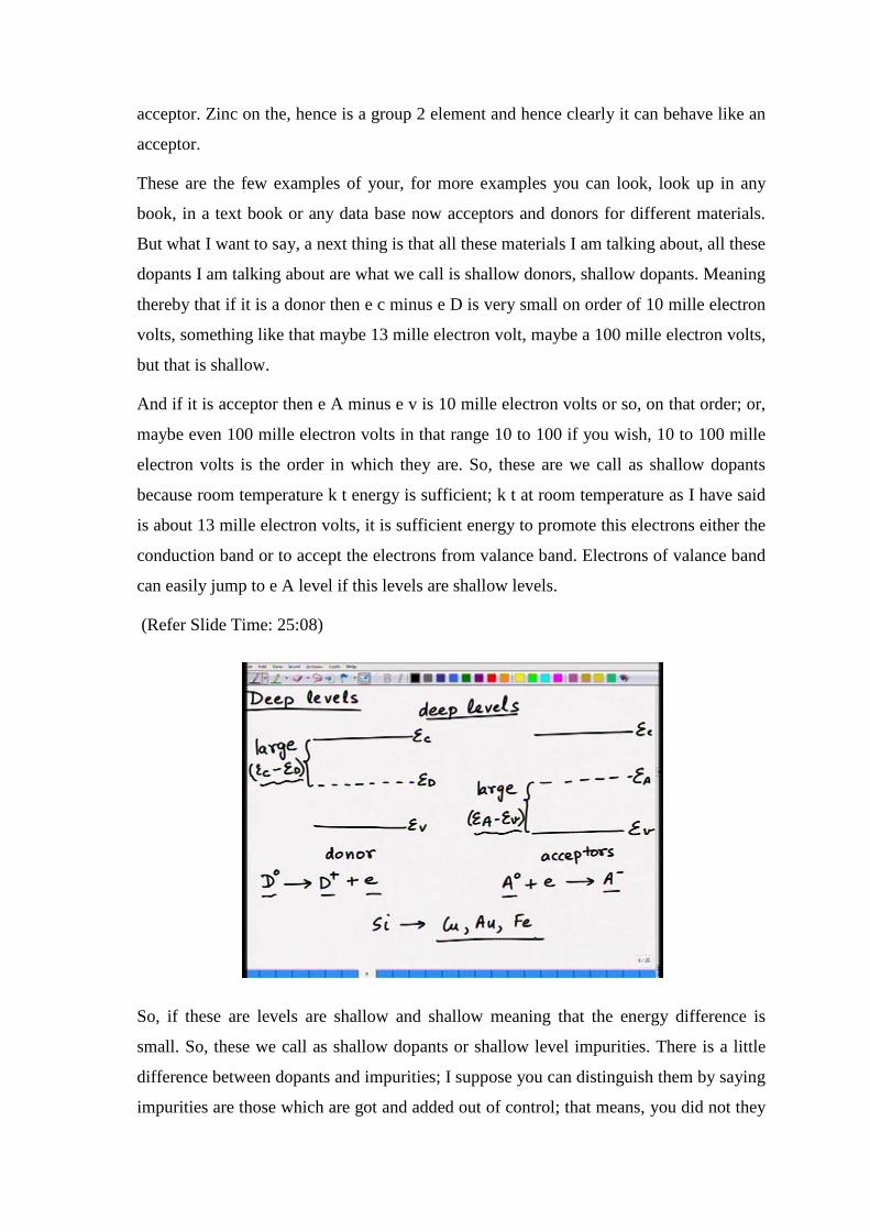
(Refer Slide Time: 25:08)
So, if these are levels are shallow and shallow meaning that the energy difference is
small. So, these we call as shallow dopants or shallow level impurities. There is a little
difference between dopants and impurities; I suppose you can distinguish them by saying
impurities are those which are got and added out of control; that means, you did not they

are not intentional they are just there, but you did not deliberately put them. Whereas
dopants would be those where you deliberately add them to manipulate your n and p. So,
that is what we will call as shallow levels.
Since I have introduced the name shallow levels, it is worthwhile to introduce also what
is called as deep levels. So, the name suggest that these deep levels are also, deep levels
are something where is energy will be large. So, if I have like this, e c and e v, then if the
dopant level, let us say donor, donors lie, and accepters. If the donors lie somewhere
deep large e c minus e D and e D level, or acceptors are somewhere in the middle or
even higher towards the e c, a large, then these are called deep levels.
And clearly the deep levels because this energy difference is large. And, this energy
difference is large then you can see that thermal energy may not be enough to completely
ionize these defects into, either take, cannot ionize for the dopants and to promote the
electron to conduction band or to accept the electrons from the valance band.
Notice that we have written here D as, when D has its electron bound to it, we are going
to write it in 0 charge state; that means, charge state is that since like phosphorous has its
5 electrons then 0 charge states it ionizes, then it goes to D plus; that means,
phosphorous plus with 4 electrons and a electron. Similarly, I could write here acceptor
as, acceptor like a boron with 3 electrons has 0 charge on it because boron comes with 3
electrons. So, that is why, that is a native configuration. So, that is no net charge on it,
boron when it has 3 electrons.
But, when it accepts electron because it wants 1more electron to complete the bonding,
but accepts 1 electron then it becomes ionize and it becomes A minus for example, it
becomes A minus. So, that is what I mean that if deep levels, if the levels are deep then
room temperature may not be sufficient for this acceptor to accept this electron because
it require this much energy to accept the electrons and e A minus e v amount of energy.
So, it may not be able to accept or very few maybe able to, and therefore very few of
these dopants may ionize in that case.
Similarly, this energy difference e c minus e D may be large and therefore this dopants
may not be able to ionize to deeper state there by giving the electron to conduction band,
it may not happen or it happens, it happens in very small quantities. These are therefore
deep levels. Deep levels are may, many. They have good, they have good use and they
have bad use.

For example, if you add, if you add, in silicon if you add copper or gold or iron, all these
form deep levels; what that means is that these are not going to, so, they are, they are life
time killers; that part will be taught to you little bit in future, few lectures down the line,
will be taught to you and we talk about what the, what the, how the statistics of
recombination of these carrier says, how the carriers are generated, and how the carriers
are recombining.
So far we are saying that recombination and generation rate are equal; that means, they
are thermal equilibrium, then what is the condition? But when we individually start
looking at recombination, and we individually start looking at generation process, then
we will use this concept of time also. But the point I am trying to make is these deep
level, because once a electron gets in there. Then since its energy required to ionize is so
large, so it may not ionize easily, and hence it is called as a trap level; that means, it traps
electron. It sits, once it gets it, it holds it; holds the electron. If so, then what it may
happen is that it may happen that the carrier may not be available for conduction. So, that
is the bad news.
The good news is, so good news is that if you have them, then they become the centers
where the recombination may happen. The electron can come at this center and holes can
come at this center and recombination can happen. Why that happens? That it has a large
cross section that these aspects you will understand later when it is taught to you.
However, these deep levels do have a use- good use and bad use. If you are making a
silicon devise for example, you will ensure that wherever you are making there is no
scope of copper, gold, and iron, these kind of materials reaching there.
Similarly, so these are called deep levels because the energy level is large and they act
as trap for electrons. Because they are traps, therefore they can have, they can suck up
your electrons and not let it participate in conduction. On other hand, it may provide the
level where it is suck up electrons and holes, and hence there for provide a level where
this electron and holes physically can come together and recombine with each other. So,
they have good role and bad role to play which you will learn little bit later. So, with this
let me move on to the next topic.

(Refer Slide Time: 31:06)
So, we have these dopants added, how do they ionize? Ionization of dopants. In general,
what we can do is we can write some, there is a, we can, we could have derived this
expression, but in this class we will not do that. Let us imagine like this. Suppose, you
have a ionization reaction going like this. That I have any dopant, a donor dopant, let us
call it D. D goes to, is exist right now in charge state, n plus. This n plus may be equal to
0 also. So, n may be 0 also, as I have written mine example earlier. And, what it happens
is that it becomes D, one additional charge state was the charge state, plus electron.
Suppose this happens, or if this happens then without deriving I will give you an
expression saying that number of, I just define the symbol in a second; the ratio of this,
not x, but other D, I would write, exponential of. So, this energy e v, e c, and e D n is this
energy level; e D n is that energy level which is indicated there, then we say that fraction,
you think of this is a fraction. We think of this, let me try to explain this like this, that
this is number of D and plus 1, plus kind of stresses per volume, divided by number of
sites for this D per unit volume, this what this quantity is.
Similarly, this quantity therefore will be equal to n D n plus divided by n sites, meaning
thereby that this is the number or number of the, if this is the for consider, for example,
phosphorous atoms. So, you think phosphorous is going on substitutional sides of silicon,
then this is number of phosphorous atoms which are in.
In fact, let us choose this is example; suppose n is 0; n is equal to 0 here; this n charge
which I am showing you 0 implying therefore imagine this D 0, a donor D is going to D

plus plus electron. Then this quantity D 0 would indicate that this will be number of D
atoms in 0 charge state divided by number of sites D can go per unit volume of course;
of both per unit same bases, per unit volume, number of a sites for D atom.
For example, if it is in silicon, then its number of site possible for silicon atom, that is
what it means number of silicon atoms per unit volume. Number of silicon set atoms
sites per unit volume is the denominator and numerator is number of this phosphorous
atom, D atoms per unit volume.
(Refer Slide Time: 35:41)
So, in that sense, then if this number of sites are the same in both the cases for these
defects, they both of silicon sites, in that case this ratio also indicates ratio of number of;
so, I can write this whole expression also as number of D n plus 1 in plus site state
number of D n n plus state as being equal to same exponential which is e D n minus e f
by k B T. So, the number per unit volume, in this state and in this state, ratio of these 2 is
given by this particular expression. Thus the ionization, how the ionization occurs, how
much is ionizing, from, ratio between one state to other state.
Now let us continue. Now we will next go to acceptor behavior. So, similarly let us write
down for acceptors also. If we have a acceptor reaction which is going on like this, let us
say x of n minus 1 charge state goes to, it accepts electron, it takes electron and becomes,
goes to n, one more additional charge state, and plus 1 negative charge state. If so, then
number of, by same token, number of this species, A n plus 1, minus per unit volume,

number of A this n minus ratio of this, then is simply given by exponential. These are the
ratio in which the ionization occurs, alright.
(Refer Slide Time: 37:41)
With this let me now restrict my attention to monovalent impurities or dopants, as earlier
we considered, the same thing- dopants are intentional, impurities are unintentional.
What do I mean by that? When I am writing this n minus, n plus, what I mean is, they are
impurities. For example, sulphur which could go to s minus 1 state, it could, from s
minus state it could go to s 2 minus state, it could go to second electron also and get 2
minus state also, these are multivaliant impurities. And hence we have been using the
symbol n, that means, sulphur 1 minus 1 state, accepting 1 more electron and becoming
sulfur 2 negative, that kind of acceptor level also exists, which is why I have given you
more general expression.
But, if we are talking about monovalent impurities, in that case what we mean is that
exactly 1 ionization occurs; that means, we either have donor in 0, in neutral state and
that becomes in plus state and gives a electron; whereas acceptor in neutral state accepts
electron and gives you A minus state. This is monovalent, because it is a only one
ionization level- from 0 to plus 1, or 0 to minus 1. In general from any charge state to
another charge state different by only 1, and that is only reaction possible, no other
reaction is possible; that is what is meant by monovalent impurity dopant.
If so, then we will restrict this, we will write down expression back again. For donors we
had in the plus extra charge state divided by in the original charge state. So, we write this

as D plus. So, we can write this as, now you use different symbol. I use capital N now
which is more commonly used in this case, N D plus divided by N D in 0 charge state
should be equal to e to power, I am using this formula here; e to power e D minus e f. So,
e D minus e f by k B T.
And similarly, I am going to write here. And this small, I am using same small n, instead
of small n I am started to write capital N which is number of D plus type of, D plus
ionize atoms, for example, phosphorous if you thinking, number of phosphorous atoms
which are ionized, which are given fifth electron. So, they only left with 4 electrons that
is. So, a question asked is, that if this is phosphorous, then I would have given P plus and
electron- some phosphorous returning its fifth electron and some electrons have been
given away by phosphorous, and hence it is in P plus state.
So, and then question asked is what is the ratio of the two, how much are they, number of
them per unit volume. And, that number is this capital N I am showing you, number of
such, number of atoms in such state, impurity atoms in such state per unit volume.
Therefore, similarly, using this expression I can write number of A in minus state
divided by N of A in 0 charge state should be equal to e to power e f minus e A by k T.
Now let us make a picture of it and can see what it means.
(Refer Slide Time: 41:22).
What it means is as this. So, I have, this is e c and this is e v. Let us say that I have
certain acceptor level. So, let us show them the acceptor levels right here. And, I also
have; and some of these acceptors which I have shown here, some ion 0 charge state; that

means, they are not occupied, and some have taken away their electron. They have taken;
it is electron, some are having electrons; they have accepted electrons; meaning thereby
they can indicate them as A minus, and this is state A minus, and this state A minus.
Whereas, the ones which have not accepted the electrons are in state A 0, A 0, A 0, A 0,
and this is e A level; and total number of such states, number of acceptors I have added
let us say is n of A; that is the total number of, I am showing here 1, 2, 3, 4, 5, 6, 7,
acceptors states. So, I am thinking of N A has been 7. And, this quantity of course being
equal to what is in 0 charge state, plus N A in minus charge state. These are 2 charge
states that are existing. And we had already know what the ratio of these two are, how
are they, what is the statistic of this ionization process.
Similarly, we think of these as the donor level. And, in the donor level I think of some
sitting bound to electrons; some electrons are bound. Fifth electron in phosphorous for
example, is bound; here is like this. And in some cases electron has been given away,
electron has been given away. So, this is e D level, this is e D level, and I have total
number of such in this example shown 1, 2, 3, 4, 5, 6, total number of donors like
phosphorous atoms that I have added are 6 for example, and some of them have ionized;
that means, they have N D plus meaning thereby here it is, this one is ionized, so this is
N D plus; and this one is ionized, so this is N D plus, N D plus, because it has given its
electron to the conduction band.
Whereas, and some of them have not given the electrons, they are still in 0 charge state;
net charge state is 0; plus n with the electron there fifth electron. So, this is N D 0, this is
N D 0, this is N D 0, or I should not say N D s. So, this is not N D 0, but D 0, this is D
plus, and this is D 0, and this is D 0, and this is D plus, and this is D plus, the ones which
have given away their electrons.
I hope that gives you idea of what these statistics are. Here is one statistics; that means,
the one, the ratio in which these two are present are given by this ratio in which this and
this are present are, is given by this expression. So, if so, our question becomes back
again, alright. Let us manipulate this little bit more.

(Refer Slide Time: 45:16).
(Refer Slide Time: 45:34)
Let us just copy, let us copy; write down this statements one more time and continue on
this for a few more minutes. N D plus divided by N D 0 as equal to e to power e D minus
e f, and N A minus, this N A minus divided by N A 0 as e to power e f minus e A by k B
T, alright. If so, also I know that N D is equal to N D 0 plus N D plus; and, N A is equal
to, this is the total, this is the amount I know, I have added. This is the amount that I have
actually added and I am asking a question, how are this split, what are I have added, how
much have given it fifth electron here in this case, and how much has how many have
not given the fifth electron.

Similarly, when I add so much acceptors- how many have accepted electrons which is
this one, and how many have not accepted electrons which is this one, how many are
these that is what we are asking. So, sum of the two therefore is 0, or is N A. If so, then
what we will do is that instead of this ratio we will use this expression, and we are going
to write this as therefore N D. So, I eliminate N D 0 in this, and instead write, will
eliminate N D 0 in this. So, I am going to write this as N D plus, divided by N D minus,
N D plus as equal to, e to power e D minus e f by k B T, which I am going to write there
for us.
Inverse of that; N D minus N D plus divided by N D plus as e to power e D minus e f by
k B T; and, this I am going to write this as N D divided by N D plus, equal to 1 plus this
quantity right here; and then, this going to, let us just carry out this. So, and then take
inverse of this. If I take inverse of this, therefore I will write N D plus by N D; therefore
the total amount that I have added; what fraction of total amount has ionized, that is the
question we are asking; should be therefore equal to 1 divided by 1 plus, e to power.
And by same token, similarly, you would get an expression where you write this as,
sorry, when we write this, invert this, so in that case mistake here, an error here. When
we invert this then we should have write it as, this as e f minus e D is what I should write
here, as k B. And, by same means, same way, N A, following this N A minus by N A
should be, this is A total N A now; total N A should be equal to 1 by 1 plus e to power e
A minus e f by k B T, alright. So, this is fraction of total which I have added, how much
of that has ionized; that is what therefore indicates.
Now, you would often, sometime see, now often in some books you will find a factor
included here; for example, I am going to write with some blue pen that a factor,
something like 2 or 4 added here; factor of 2 or 4 added in here. This factor you could
add, but I do not want to get into this; about, I do not want to add. This has something to
do with this pen available and this has also something to do with, this is degeneracy of
the levels, this is something do with degeneracy; remember valance band, split of bands
and a regular band was coming very close to each other, something to do with this fact
which I will not include in this course.
Once I add this, they will include it there; then what I can do is, I can express this 4 as
exponential or something quantity. Whatever that is, exponential I can take it inside this
e in here and include it in e, and write this as a effective e A; I can proceed this way and

therefore effectively I can remove what is in the front. So, as long as you imagine this, so
I am not going to add this in here; I have decide to remove it; I will leave at that. In some
books if, when you read you will find a factor in front of it, but it is always possible to
include that our factor also into the exponential. And then effectively, then values of e A
and this e D will somewhat change; that is about it. So, I will not include in my lectures
right here.
(Refer Slide Time: 51:05)
Now, next question is that if I want, suppose temp now I mean saying that if the levels
are shallow; this is e c, this is e v, if this levels are shallow, that means, we are saying the
sufficient thermal energy that this electrons can jump in here, the electrons can jump in
here, the electrons can jump in here also, the electrons can jump here at this levels which
means whatever acceptor have added all of it becomes ionized, and whatever donors are
added they become ionized because they give their electron to the conduction band.
What that means in the picture is when complete ionization occurs, complete ionizations
occur, occurs then in that case approximately N D plus by N D is almost equal to 1, and
N A minus by N A is almost equal to 1 is what we are saying. That means, whatever we
added all that have ionized because everything, all the electrons went in near; all the
acceptors accepted the electrons and they became. So, all the phosphorous atoms and
silicon gave the fifth electrons away. So, they became ionized. So, N D plus value is
same thing as whatever we have added. Similarly, if we have added boron each boron

atom has accepted. So, therefore N A minus is the same value as whatever we added; this
is approximately equal to 1.
So, you imagine like this that they approx, this is the process, this is a condition where
we call as complete ionization. In that case, we can, in the next lecture I will show you a
problem, I will solve the problem of this complete ionization. Remember at the end of
day in intrinsic case we have found, what value of n and p are? We know that n is equal
to p as its value is n i, and n i we have calculated, and I will show you that.
Now, when I have done the doping I am again in thermal equilibrium, interested in
knowing what the value of n and p are? What is the value of n in number of electrons in
conduction band, what is the number of holes in the valance band; that is the number we
are interested in. So, now, when we have doped it, we are going to do it for two cases.
Now, one, first case is when temperature is high enough, and therefore complete
ionization occurs. All the electrons are able to, from donor level they go to conduction
band, the electrons in valance band are able to jump to the acceptor level.
In the next lecture I will start with that and show to you under complete ionization what
the values of n and p are? Then what will we do is we will start moving to low
temperatures and see how, when the ionization is, when the assumption of complete
ionization is not appropriate; that means, ionization is incomplete then what happens to n
and p. Those are the 2 questions which we will answer in next 2 lectures.
Thank you. .