Solution-processed bismuth halide thin film semiconductors ...
168
Graduate eses and Dissertations Iowa State University Capstones, eses and Dissertations 2019 Solution-processed bismuth halide thin film semiconductors for photovoltaic application Umar Hussein Hamdeh Iowa State University Follow this and additional works at: hps://lib.dr.iastate.edu/etd Part of the Chemical Engineering Commons is Dissertation is brought to you for free and open access by the Iowa State University Capstones, eses and Dissertations at Iowa State University Digital Repository. It has been accepted for inclusion in Graduate eses and Dissertations by an authorized administrator of Iowa State University Digital Repository. For more information, please contact [email protected]. Recommended Citation Hamdeh, Umar Hussein, "Solution-processed bismuth halide thin film semiconductors for photovoltaic application" (2019). Graduate eses and Dissertations. 17198. hps://lib.dr.iastate.edu/etd/17198
-
Upload
khangminh22 -
Category
Documents
-
view
0 -
download
0
Transcript of Solution-processed bismuth halide thin film semiconductors ...

Graduate Theses and Dissertations Iowa State University Capstones, Theses andDissertations
2019
Solution-processed bismuth halide thin filmsemiconductors for photovoltaic applicationUmar Hussein HamdehIowa State University
Follow this and additional works at: https://lib.dr.iastate.edu/etd
Part of the Chemical Engineering Commons
This Dissertation is brought to you for free and open access by the Iowa State University Capstones, Theses and Dissertations at Iowa State UniversityDigital Repository. It has been accepted for inclusion in Graduate Theses and Dissertations by an authorized administrator of Iowa State UniversityDigital Repository. For more information, please contact [email protected].
Recommended CitationHamdeh, Umar Hussein, "Solution-processed bismuth halide thin film semiconductors for photovoltaic application" (2019). GraduateTheses and Dissertations. 17198.https://lib.dr.iastate.edu/etd/17198

Solution-processed bismuth halide thin film semiconductors for photovoltaic
application
by
Umar Hussein Hamdeh
A dissertation submitted to the graduate faculty
in partial fulfillment of the requirements for the degree of
DOCTOR OF PHILOSOPHY
Major: Chemical Engineering
Program of Study Committee:
Matthew G. Panthani, Major Professor
Andrew C. Hillier
D. Raj Raman
Eric W. Cochran
Javier Vela-Beccera
The student author, whose presentation of the scholarship herein was approved by the
program of study committee, is solely responsible for the content of this dissertation. The
Graduate College will ensure this dissertation is globally accessible and will not permit
alterations after a degree is conferred.
Iowa State University
Ames, Iowa
2019
Copyright © Umar Hussein Hamdeh, 2019. All rights reserved.

DEDICATION
I would like to dedicate my work to my family for their love and support. I’d like to
thank my parents Hussein and Amal, my siblings Tania, Samir, Yusuf, Ahmad, Tala, Waleed,
Deema, and Sami, and my niece and nephews Yasmeen, Ehab, and Layth. It’s your
unconditional love that gives me the strength and confidence to overcome all challenges.

iii
TABLE OF CONTENTS
Page
LIST OF FIGURES .................................................................................................................. v
NOMENCLATURE ................................................................................................................ ix
ACKNOWLEDGMENTS ....................................................................................................... xi
ABSTRACT ............................................................................................................................ xii
CHAPTER 1. INTRODUCTION ............................................................................................. 1
CHAPTER 2. REVIEW OF LITERATURE .......................................................................... 11
2.1. Introduction .................................................................................................................. 11
2.2. Pb(II)-Halide Perovskites............................................................................................. 12
2.3. Bi(III)-Halide and Bi(III)-Halide Perovskites ............................................................. 27
2.4. Conclusions and Summary .......................................................................................... 35
2.5. References .................................................................................................................... 37
CHAPTER 3. SOLUTION-PROCESSED BISMUTH TRIIODIDE THIN-FILMS FOR
PHOTOVOLTAIC APPLICATION ...................................................................................... 52
3.1. Abstract ........................................................................................................................ 52
3.2. Introduction .................................................................................................................. 53
3.3. Experimental Methods ................................................................................................. 55
3.4. Results and Discussion ................................................................................................ 61
3.5. Summary and Conclusions .......................................................................................... 84
3.6. Acknowledgments........................................................................................................ 84
3.7. References .................................................................................................................... 85
CHAPTER 4. THE EFFECTS OF SOLVENT COORDINATION STRENGTH ON THE
MORPHOLOGY OF SOLUTION-PROCESSED BISMUTH TRIIOIDE THIN FILMS ..... 91
4.1. Abstract ........................................................................................................................ 91
4.2. Introduction .................................................................................................................. 91
4.3. Experimental Methods ................................................................................................. 94
4.4. Results and Discussion ................................................................................................ 97
4.5. Summary and Conclusions ........................................................................................ 113

iv
4.6. Acknowledgments...................................................................................................... 113
4.7. References .................................................................................................................. 113
CHAPTER 5. SOLUTION-PROCESSED BISMUTH HALIDE PEROVSKITE THIN
FILMS: INFLUENCE OF DEPOSITION CONDITIONS AND A-SITE ALLOYING ON
MORPHOLOGY AND OPTICAL PROPERTIES .............................................................. 120
5.1. Abstract ...................................................................................................................... 120
5.2. Introduction ................................................................................................................ 121
5.3. Experimental Methods ............................................................................................... 123
5.4. Results and Discussion .............................................................................................. 126
5.5. Summary and Conclusions ........................................................................................ 143
5.6. Acknowledgments...................................................................................................... 143
5.7. References .................................................................................................................. 144
CHAPTER 6. CONCLUSIONS AND SUMMARY ............................................................ 149

v
LIST OF FIGURES
Figure 3.1. Depiction of solvent vapor annealing. Solvent is placed on the blank glass
substrate on the furthest corner from the sample. A glass petri dish is used to
contain the solvent vapor. ......................................................................................... 60
Figure 3.2. (a) Absorbance spectra of a BiI3 thin film (black), and BiI3 dissolved in THF
(red), DMF (green) and ethanol (EtOH, blue). (b) Photographs of BiI3
dissolved in THF, DMF, and ethanol at 100 mg/mL ............................................... 62
Figure 3.3. Unit cells of BiI3 complexes with (a) THF and (b) DMF solvent. ............................ 63
Figure 3.4. (a) Thickness of BiI3 versus concentration of BiI3 solution. Thickness
determined by AFM. (b) Percent transmission of ~200 nm thick BiI3 thin film ...... 65
Figure 3.5. Absorbance of a ~200 nm thick BiI3 thin-film. Inset: Tauc plot for BiI3 thin
film. .......................................................................................................................... 65
Figure 3.6. Photographs of BiI3 thin films deposited with (a) THF as coordinating solvent
or (b) DMF as coordinating solvent after spin coating. Adding HI to THF
resulted in a film like (b). ......................................................................................... 66
Figure 3 7. SEM images of the surface of substrates processed in a N2-filled glovebox with
varying processing conditions: (a) No SVA (b) THF SVA (c) DMF SVA ............. 67
Figure 3 8. XRD of BiI3 thin films processed in a N2-filled glovebox with varied SVA
conditions. ................................................................................................................ 68
Figure 3.9. SEM image of BiI3 thin films processed with DMF solvent vapor at (a) 5,000x
magnification and (b) 15,000x magnification. ......................................................... 69
Figure 3.10. Schematic of the device structure and SEM cross-section. ..................................... 70
Figure 3.11. (a) X-ray photoelectron spectroscopy of thin films processed in a N2-filled
glovebox and in ambient air. (b) J-V characteristics of BiI3 PVs processed in a
N2-filled glovebox and in ambient air. ..................................................................... 71
Figure 3.12. Atomic percentage of elements in BiI3 film as a function of etch time. .................. 71
Figure 3.13. Grazing incidence x-ray diffraction of oxidized BiI3 showing the formation of
BiOI. ......................................................................................................................... 72
Figure 3.14. Plan-view SEM images BiI3 thin films processed without SVA a) in N2 and b)
in air .......................................................................................................................... 73
vi
Figure 3.15. Plan-view SEM images BiI3 thin films processed with THF SVA a) in N2 and
b) in air ..................................................................................................................... 74
Figure 3.16. Plan-view SEM images BiI3 thin films processed with DMF SVA a) in N2 and
b) in air ..................................................................................................................... 74
Figure 3.17. Cross sectional SEM images with TLD detector of (a) No SVA BiI3 PV
device, and (b) DMF SVA BiI3 PV device both processed in air. ........................... 75
Figure 3.18. Plan-view SEM images BiI3 thin films processed in air with a) No SVA b)
THF SVA c) DMF SVA ........................................................................................... 75
Figure 3.19. J−V characteristics under AM1.5 illumination of BiI3 thin films processed
without SVA, with THF SVA, and with DMF SVA . .............................................. 76
Figure 3.20 (a) The effect of varying the processing temperature on the JSC of BiI3 thin
films without SVA. (b) The effect of varying the DMF SVA temperature on
the JSC of BiI3 PV devices. ....................................................................................... 77
Figure 3.21. The effect of post deposition annealing and champion device IV sweep. .............. 78
Figure 3. 22. (a) External quantum efficiency (EQE) of BiI3 thin films processed without
SVA, with THF SVA, and with DMF SVA. (b) Steady-state
photoluminescence (PL) spectra of BiI3 processed without SVA, with THF
SVA, and with DMF SVA. (c) Photoluminescence lifetime of BiI3 processed
in N2, and in air . ....................................................................................................... 79
Figure 3.23. The effect of processing conditions on device (a) transmittance, (b)
reflectance, and (c) absorbance on BiI3 thin films. .................................................. 80
Figure 3.24. (a) The effect of SVA on PL carrier lifetime. IRF is the instrumental response
function. (b) Comparison of PL carrier lifetime between in air and N2-
processing.. ............................................................................................................... 81
Figure 3.25. The effect of varying metal oxide hole transport layers for BiI3 PV devices. ......... 83
Figure 3.26. Energy band diagram of the materials used in the study. ........................................ 83
Figure 4.1. Properties of complexing solvents used in this study. ............................................... 98
Figure 4.2. Representative mechanism of the decomplexation, nucleation, and growth
process of the BiI3 film alongside a representative demonstration of the
observed color change of films as the decomplexation proceeds. ............................ 99
Figure 4.3. UV-Vis absorbance of the BiI3 thin films exhibiting solvent decomplexation
over time.. ................................................................................................................. 99

vii
Figure 4.4. FT-IR characterization of BiI3 thin films with and without thermal annealing
and with a chlorobenzene wash and thermal annealing deposited from (a) THF,
(b) DMF, (c) NMP, and (d) DMSO. ....................................................................... 100
Figure 4.5. SEM images of BiI3 thin films from solutions of 400 mg/mL of BiI3 dissolved
in (a) THF, (b) DMF, (c) NMP, and (d) DMSO, where DN and vapor pressure
in mmHg (Pvap) are indicated. ................................................................................. 102
Figure 4.6. Scherrer analysis of BiI3 films deposited from neat ligand (THF, DMF, NMP,
DMSO) and solvent additive:BiI3 (1:1, 1:2, and 1:5) dissolved in THF on glass
substrates. ............................................................................................................... 103
Figure 4.7. Scherrer analysis of BiI3 films deposited from neat ligand (THF, DMF, NMP,
DMSO) and solvent additive:BiI3 (1:1, 1:2, and 1:5) dissolved in THF on ITO
substrates. ............................................................................................................... 103
Figure 4.8. XRD of BiI3 thin films deposited from neat ligand (THF, DMF, NMP, DMSO)
and solvent additive:BiI3 (1:1, 1:2, and 1:5) dissolved in THF on glass
substrates. ............................................................................................................... 104
Figure 4.9. XRD of BiI3 thin films deposited from neat ligand (THF, DMF, NMP, DMSO)
and solvent additive:BiI3 (1:1, and 1:2) dissolved in THF on ITO substrates. ...... 105
Figure 4.10. SEM of films processed from BiI3 in THF with different solvent additives of
(a) GBL, (b) DMF, (c) NMP, (d) DMSO, (e) DMPU, and (f) DEA. ..................... 108
Figure 4.11. Various ratios of solvents in THF; (a-c) DMF, (d-f) NMP or (g-i) DMSO. The
ratios of solvent:BiI3 were (a,d,g) 1:1, (b,e,h) 1:2 or (c,f,i) 1:5.. ............................ 110
Figure 4.12. J-V characterization of BiI3 thin films solar cells fabricated in ambient air (RH
50-60%) and N2-filled glovebox. DMF (1:2 DMF:BiI3), NMP (1:5 NMP:BiI3),
and DMSO (1:5 DMSO:BiI3) solvent additives were used for device
characterization. ...................................................................................................... 111
Figure 4.13. SEM of films processed from BiI3 in THF with 1:2 solvent additives:BiI3. In
ambient air (RH 50 -60%) (a) No SA, (b) DMF, (c) DMSO, (d) NMP. In N2-
filled glovebox (e) No SA, (f) DMF, (g) DMSO, (h) NMP. .................................. 112
Figure 5.1. Characterization of films produced using the single-step deposition. SEM
images of (a) Rb3Bi2I9, (b) Cs3Bi2I9, (c) MA3Bi2I9, and (d) FA3Bi2I9 films. (e)
Tauc plots of diffuse-reflectance absorption. ......................................................... 127
Figure 5.2. (a) SEM image of a BiI3 thin film. (b) Image of a BiI3 thin film prior to two-
step deposition. (c) Image of MA3Bi2I9 thin film post two-step deposition. Film
color representative of A3Bi2I9 films. (d) UV-Vis characterization of BiI3 and
A3Bi2I9 thin films .................................................................................................... 128

viii
Figure 5.3. XRD characterization of initial BiI3 thin film and two-step A3Bi2I9 (A = FA+,
MA+, Cs+, and Rb+) thin films deposited on TiO2 coated FTO substrates. ............ 128
Figure 5 4. XRD characterization of one- and two-step (a) FA3Bi2I9 and (b) MA3Bi2I9 thin
films deposited on TiO2 coated FTO substrates. .................................................... 129
Figure 5.5. XRD characterization of one- and two-step (a) Cs3Bi2I9 and (b) Rb3Bi2I9 thin
films deposited on TiO2 coated FTO substrates. .................................................... 130
Figure 5.6. Effect of the acidified IPA/H2O solution on the absorbance spectra of a BiI3
thin film. The acidified IPA/H2O solution was spin coated onto the BiI3 film to
mimic the conditions of the two-step deposition procedure. .................................. 131
Figure 5.7. (a) UV-Vis and (b) XRD characterization of two-step A3Bi2I9 (A= FA+, MA+)
thin films fabricated from IPA and the acidified IPA/H2O solution. ..................... 132
Figure 5.8. SEM characterization of two-step A3Bi2I9 (A= FA+, MA+) thin films fabricated
from IPA and the acidified IPA/H2O solution. ....................................................... 133
Figure 5.9. Characterization of films produced using the two-step deposition. SEM images
of (a) Rb3Bi2I9, (b) Cs3Bi2I9, (c) MA3Bi2I9, and (d) FA3Bi2I9 thin films. (e)
Tauc plots of diffuse-reflectance absorption. ......................................................... 134
Figure 5.10. SEM images of two-step A3Bi2I9, (A = FA+, MA+, Cs+) thin films with
varying AI salt concentrations. ............................................................................... 134
Figure 5.11. XRD characterization of A3Bi2I9 (A = FA+, MA+, Cs+, Rb+) films produced
from the (a) single-step and (b) two-step deposition. ............................................. 136
Figure 5.12. XRD of one-step AxRb3-xBi2I9 (A= FA+, MA+, Cs+) thin films deposited on
TiO2 coated FTO substrates. ................................................................................... 137
Figure 5.13. XRD of two-step AxRb3-xBi2I9 (A= FA+, MA+, Cs+) thin films deposited on
TiO2 coated FTO substrates .................................................................................... 138
Figure 5.14. (a) XRD of AxRb3-xBi2I9 films deposited using the single-step deposition
procedure. (b) Band gaps for the one- and two-step deposition of AxRb3-xBi2I9
films are plotted as a function of d001-spacing. ....................................................... 141
Figure 5.15. Vegard’s law analysis for one- and two-step AxRb3-xBi2I9 (A= FA+, MA+) thin
films. ....................................................................................................................... 141
Figure 5.16. Normalized Tauc plots of the KM data for the (a) one- and (b) two-step
AxRb3-xBi2I9 (A = FA+, MA+, Cs+) thin films assuming indirect bandgaps. .......... 142

ix
NOMENCLATURE
PV Photovoltaics
LCOE Levelized Cost of Energy
CIGS Copper Indium Gallium Selenide
CdTe Cadmium Telluride
CZTS Copper Zinc Tin Sulfide
MAPbI3 Methylammonium Lead Iodide
TF Tolerance Factor
FAPbI3 Formamidinium Lead Iodide
PEA Phenylethylammonium
BA Butylammonium
CQD Colloidal Quantum Dots
QD Quantum Dots
LED Light Emitting Diodes
QD-LED Quantum Dot Light Emitting Diodes
XRD X-Ray Diffraction
GIXRD Grazing Incidence X-Ray Diffraction
XPS X-Ray Photospectroscopy
SEM Scanning Electron Microscopy
AFM Atomic Force Microscopy
PL Photoluminescence
TRPL Time-resolved Photoluminescence
UV-Vis Ultraviolet-Visible

x
SVA Solvent Vapor Annealing
EQE External Quantum Efficiency
THF Tetrohydrofuran
DMF N.N-Dimethylformamide
DMSO Dimethylsulfoxide
NMP N-Methyl-2-Pyrrolidone
HI Hydroiodic Acid
JSC Short-circuit Current Density
VOC Open-circuit Voltage
FF Fill factor
PCE Power Conversion Efficiency
J-V Current-Voltage

xi
ACKNOWLEDGMENTS
I would like to thank my major professor, Dr. Matthew G. Panthani, your patience and
guidance helped me become a better scientist and a better person. I benefited tremendously by
working in your laboratory, and I am very grateful for the opportunity you gave me. Next, I’d
like to thank my committee members, Dr. Andrew Hillier, Dr. Eric Cochran, Dr. Javier-Vela
Beccera, and Dr. Raj Raman for their guidance and support throughout the course of this
research.
In addition, I would like to thank all the wonderful people that I have had the opportunity
to collaborate with here at Iowa State University. I would like to thank my lab mates Rainie
Nelson, Yujie Wang, Atefe Hadi, Bradley Ryan, and Utkarsh Ramesh. Next, I would like to
thank the undergraduates who I’ve had the pleasure of both mentoring and befriending. This
includes Christian Pinnell, Bryan Cote, Quinn Pollock, Iver Cleveland, Kevin Prince, Michael
Zembrzuski, and Jonathon Slobidsky. Lastly, I’ve benefited greatly from the guidance I received
from other faculty and staff at Iowa State. I would like to thank Dr. Matt Besser with the Ames
Laboratory, Dr. Ellern Arkady with the Chemical Instrumentation Facility, and Dr. Vikram Dalal
and Max Noack with the Microelectronics Research Center.
Financially, I am thankful for the generous support of the BEI Presidential Fellowship,
and the Trinect Fellowship. I would like to thank Dr. Joanne Olson and the entire Trinect staff
for giving me the opportunity to work with a 3rd and 4th grade class. It is an experience I will
cherish for the rest of my life. Next, I’d like to thank all my friends, the department faculty, and
staff at Iowa State University. You made this an enjoyable experience. Finally, I’d like to thank
all the scientists before me. This work stands on the shoulders of many and I am honored to
contribute to the total body of work with this dissertation.

xii
ABSTRACT
Hybrid organic-inorganic Pb halide perovskite semiconductors have shown excellent
promise in a wide variety of optoelectronic applications; the impressive performance can be
attributed to their excellent optoelectronic and charge transport properties. Unfortunately, hybrid
organic-inorganic Pb halide perovskites suffer from intrinsic instabilities and contain a toxic Pb
component. The focus of this PhD dissertation is in the development of alternative
semiconductors that are predicted to share these excellent properties without the toxicity and
stability concerns. Bi halide semiconductors could have the greatest potential as nontoxic and
stable alternatives to hybrid organic-inorganic Pb halide perovskites due to the chemical
similarity of Bi(III) and Pb(II). Of interest are BiI3 and A3Bi2I9 (A = FA, MA, Cs, Rb)
compounds.
The present challenge facing BiI3 and A3Bi2I9 optoelectronic devices are the poor film
morphology. Annealing BiI3 thin films in DMF vapor at relatively low temperatures (≤ 100 °C)
resulted in increased grain size and crystallographic reorientation within the films. Non-
optimized BiI3 solar cells achieved power conversion efficiencies of 1.0%, demonstrating the
potential of BiI3 as a non-toxic and air-stable semiconductor for photovoltaic applications. Next,
using BiI3 as a model system, we demonstrated that the film morphology and surface coverage
are strongly dependent on the Gutmann donor number of Lewis base solvents. We demonstrate
that coordinating BiI3 with a combination of solvents with high and low donor numbers results in
conformal films that have been difficult to achieve using conventional solution-based deposition
techniques.
To address the challenges with film morphology with A3Bi2I9 compounds an alternative
deposition procedure was developed utilizing a two-step deposition procedure in which
xiii
optimized BiI3 thin films were converted into A3Bi2I9. Thin films fabricated from the one-step
deposition exhibited a preferred crystallographic orientation along the c-axis, while the two-step
deposition decreased this preferred orientation. Films deposited from the two-step method
exhibited increased homogeneity in the surface coverage and crystal grain sizes. After improving
the film morphology, we attempt to tune the bandgap of A3Bi2I9 compounds. The bandgap is too
wide for application in a single junction photovoltaic device. To tune the bandgap, we attempted
to induce chemical pressure in the crystal structure through cation size mismatch. We determined
that the bandgap is insensitive to A-site tuning because A3Bi2I9 compounds predominantly form
a 0D structure that limits variations to the bandgap.

1
CHAPTER 1. INTRODUCTION
Bearing in mind the recent advancements of developing countries and the growing
concern from the extensive use of fossil fuels on the environment, the need for an abundant clean
source of energy is imperative to the sustainability and future growth of humanity. Sunlight is
arguably the best source for an indefinite clean energy source and the production of solar cells
could facilitate sustainable economic growth. The theoretical potential of solar power is roughly
90,000 TW,1 while our global energy consumption in 2016 was slightly less than 31 TW.2 In
other words, more energy is striking the Earth’s surface in three hours than the worldwide energy
consumption in 2016. This thermotical potential is assuming that 100% of the sunlight is
converted into usable electricity and that the entire surface of the Earth is being utilized to
convert solar energy, both of which are not feasible. Assuming 20% conversion of sunlight, we
would need to cover approximately 890 thousand km2, or 0.17% of the Earth’s surface, with
solar cells to meet the global energy consumption. This is equivalent to covering 10% of the
Sahara Desert. For the United States, which accounts for roughly 5 TW of the global energy
consumption,2 we would need to cover an area equivalent to the state of Iowa to meet our
national energy demands. Installation of solar panels on rooftops of commercial and residential
buildings and building integrated photovoltaics (PVs) can significantly reduce the land required
for solar panels. Currently, solar energy only accounts for 1.6% of the total quantity of electricity
generated in the U.S.3 Over the next 25 years the Energy Information Administration predicts
that roughly 50% of the new energy capacity will be renewable energy sources, such as solar and
wind.4 This highlights both the potential of utilizing sunlight as an alternative energy source and
the economic impetus to convert sunlight into usable electricity.

2
There are several cost factors to consider when comparing the economic feasibility of
building power plants utilizing certain energy sources to produce electricity. Currently, one of
the drawbacks of using conventional or first-generation PVs is the higher cost of solar power
compared to oil and gas fuel plants. The overnight capital cost is the cost of building a new
power plant “overnight” and is used in the power generation industry to compare economic
feasibility of building various power plants. The U.S. Energy Information Administration
estimates the overnight capital cost for a new gas/oil combined cycle power plant is $1000/kW
while the costs for a new solar PV plant is $1800/kW.4 However, once the solar plant is
operational, it does not incur fuel costs, while fuel costs and supply can vary significantly for gas
and oil fuel plants. A more consistent comparison of the cost of electricity generation between
different energy sources can be realized through the levelized cost of energy (LCOE). The LCOE
is an economic assessment tool built by the National Renewable Energy Lab which takes the
average total cost to build and operate a power plant divided by the total energy output over the
plant’s lifetime.5 When comparing the estimated 2023 LCOE of solar PV plants to gas/oil
combined cycle power plants the total system LCOE is $48.8/MWh and $42.8/MWh (2018
$/MWh) respectively.6 The LCOE predicts that solar PV plants will be more competitive in the
future, but further reduction in manufacturing costs is necessary for implementation of solar PV
technology over gas/oil power plants.
Presently, over 90% of the solar cell market utilizes crystalline silicon (Si). To produce
ultra-high-purity Si wafers necessary for solar cell application highly energy intensive processing
is necessary, which increases the cost of manufacturing significantly. Current practices for
producing crystalline Si include growing Si wafers at temperatures up to 1,400 °C and then
processing the wafers further with various vapor deposition techniques. The high temperatures

3
used to produce crystalline Si is inherently inefficient and these highly energy intensive
processing conditions can inhibit the high-throughput fabrication necessary for massive and
rapid infrastructural implementation. By reducing the processing temperature, the cost of
manufacturing solar cells can be significantly decreased. Emerging PV technologies — that are
solution-processable — aim to circumvent the inherently inefficient processing techniques used
to fabricate first-generation PVs like Si. The use of solution-processable materials allows for
room temperature high throughput processing techniques processing such as roll to roll
fabrication, spray coating, and ink-jet printing. Solution-processable materials provide a low-cost
alternative to the production of traditional crystalline Si solar cell devices.
Another drawback of Si is its indirect bandgap which requires a relatively thick layer of
material to absorb enough sunlight. Si is also brittle and needs to be supported on a rigid glass
substrate, increasing the module cost further. Reducing the thickness of solar cells will reduce
feedstock and processing costs, as well as its impact on the global material reserves. Emerging
PV technologies — such as dye-sensitized solar cells and perovskite solar cells — use 1,000
times less material compared to Si solar cells. Moreover, emerging PV technologies utilize
inexpensive materials that can be fabricated on flexible supports reducing the module cost. Thin
film semiconductors have a distinct advantage over traditional crystalline Si because of improved
electronic properties, and reduced manufacturing costs. For solar PV plants to be competitive
electric generation sources in the energy market, they must decrease the $/watt to below that of
oil/gas fuel plants. The need for low-cost and high-throughput processing is necessary to meet
this future demand. Thin-film solution-processable PV devices have the potential to meet these
requirements.

4
Currently, copper indium gallium selenide (CIGS) and cadmium telluride (CdTe) are the
leaders in thin-film PV technologies. These materials have already demonstrated commercial
application, but there are still barriers that need to be overcome for their use over traditional
crystalline Si PV devices. Moreover, scalability is an issue with these material types as there is a
scarcity of these elements within the Earth’s crust. Therefore, within the PV research
community, there has been a major incentive to develop Earth-abundant materials for thin-film
PV application. Researchers has begun developing Earth-abundant materials, such as copper zinc
tin sulfide (CZTS), iron pyrite (FeS2), lead sulfide (PbS), and tin sulfide (SnS). Unfortunately, at
the rate in which the global climate is changing, the need for accelerated discovery of new Earth-
abundant materials is necessary, as well as a screening processing to determine the potential of
these newly discovered materials for use in PV devices. This screening process is necessary to
circumvent the years of research needed to determine the viability of materials for PV devices.
Brandt et al. developed strategies to expedite the development and screening of new PV
materials.26 From his work, a list of potential materials with promising PV characteristics was
developed using important criteria to judge PV materials. The criteria that was developed was
based off the unique properties found in the highly researched perovskite material
methylammonium lead iodide (MAPbI3).
Over the past decade, solution-processed inorganic and hybrid organic-inorganic
semiconductors, such as MAPbI3, have emerged as an inexpensive route for high-performance,
large-area electronics such as PVs,5-8 display technologies,9 and sensing.10-12 A number of
strategies have emerged for solution-processing inorganic materials; among these are sintered
nanocrystals,13-18 molecular precursors,19-22 and solution-processed nanocrystalline thin films.23-25
MAPbI3 and related “hybrid perovskite” materials have been of enormous interest for PVs due to

5
their ease of processing and mild deposition techniques and have quickly attained a NREL
certified power conversion efficiency (PCE) of over 23%.7 This remarkable rise in PCE over the
course of decade has been a result of rapid progress in developing precursor chemistries,28
processing conditions,29 and device architectures.30,31 However, there are still concerns regarding
the commercial viability of hybrid perovskite materials; this includes the toxicity of Pb-based
compounds32 and stability under normal operating conditions.33 When exposed to moist air for
several days34 or temperatures exceeding 85 °C,35 MAPbI3 can rapidly degrade into lead iodide
(PbI2).
To address the concern of toxicity and stability, many research groups have begun
studying related materials in hopes of achieving similarly high PCE to Pb-based hybrid
perovskites but using stable and non-toxic materials. Of these alternatives, Bi-based
semiconductors could have the greatest potential due to their chemical similarity to Pb. One of
the criteria for the success of MAPbI3 PV devices is the “defect tolerance” that arises from this
electronic configuration.26 Therefore, Bi-based semiconductors could have many of the benefits
of Pb-based semiconductors, but without the toxicity and stability concerns.
Motivated by the potential of Bi-based semiconductors, this dissertation reports on the
development of the material chemistry of bismuth triiodide (BiI3) and bismuth halide perovskite
(A3Bi2I9) thin-film PVs. Currently, there is a lack of understanding of the material chemistry of
BiI3 and A3Bi2I9 and how that relates to its PV device performance. This dissertation aims to
develop strategies to produce high-quality BiI3 and A3Bi2I9 thin-films and further understood the
material chemistry of BiI3 and A3Bi2I9. The strategies developed in this dissertation can be used
as a platform for deeper scientific inquiries into Bi halide PVs and serve to inform the reader on
the state-of-the-art fabrication techniques.

6
The dissertation will be outlined as follows: Chapter 2 is a review of Pb halide
perovskite, Bi halide, and Bi halide perovskite semiconductors pertinent to this dissertation.
Chapter 3 will focus on the material chemistry of BiI3 thin films and the fabrication of BiI3 thin
film PVs through solvent vapor annealing. Chapter 4 will focus on the utilization of solvent
additives in BiI3 thin films to further manipulate the thin film morphology. Chapter 5 will focus
on the material chemistry of Bi halide perovskite A3Bi2I9 compounds and applies the work done
in Chapter 4 to develop a two-step deposition procedure for A3Bi2I9 thin films. Chapter 6
concludes with a summary of the dissertation’s contribution and future works.
References
1. Agency, I. E. Key World Energy Statistics 2016.
http://www.iea.org/publications/freepublications/publication/key-world-energy-statistics.html
(April 18),
2. Administration, U. S. E. I. U.S. Energy Information Administration Independent S
tatistics and Analysis. (April 18),
3. Administration, U. S. E. I. EIA - Annual Energy Outlook 2017.
https://www.eia.gov/outlooks/aeo/ (April 18),
4. Administration, U. S. E. I. Updated Capital Cost Estimates for Utility Scale Electricity
Generating Plants. https://www.eia.gov/outlooks/capitalcost/pdf/updated_capcost.pdf (April 18),
5. Gur, I.; Fromer, N. A.; Geier, M. L.; Alivisatos, A. P., Air-Stable All-Inorganic
Nanocrystal Solar Cells Processed from Solution. Science 2005, 310, (5747), 462-465.
6. Graetzel, M.; Janssen, R. A. J.; Mitzi, D. B.; Sargent, E. H., Materials interface
engineering for solution-processed photovoltaics. Nature 2012, 488, (7411), 304-312.
7. Milliron, D. J.; Mitzi, D. B.; Copel, M.; Murray, C. E., Solution-Processed Metal
Chalcogenide Films for p-Type Transistors. Chemistry of Materials 2006, 18, (3), 587-590.
8. Panthani, M. G.; Akhavan, V.; Goodfellow, B.; Schmidtke, J. P.; Dunn, L.; Dodabalapur,
A.; Barbara, P. F.; Korgel, B. A., Synthesis of CuInS2, CuInSe2, and Cu(InxGa1-x)Se2 (CIGS)
Nanocrystal “Inks” for Printable Photovoltaics. Journal of the American Chemical Society 2008,
130, (49), 16770-16777.

7
9. Shirasaki, Y.; Supran, G. J.; Bawendi, M. G.; Bulović, V., Emergence of colloidal
quantum-dot light-emitting technologies. Nature Photonics 2013, 7, (1), 13-23.
10. Liu, C.; Wang, K.; Du, P.; Wang, E.; Gong, X.; Heeger, A. J., Ultrasensitive solution-
processed broad-band photodetectors using CH 3 NH 3 PbI 3 perovskite hybrids and PbS
quantum dots as light harvesters. Nanoscale 2015, 7, (39), 16460-16469.
11. McDonald, S. A.; Konstantatos, G.; Zhang, S.; Cyr, P. W.; Klem, E. J.; Levina, L.;
Sargent, E. H., Solution-processed PbS quantum dot infrared photodetectors and photovoltaics.
Nat Mater 2005, 4, (2), 138-42.
12. Nozik, A. J., Nanophotonics: Making the most of photons. Nature nanotechnology 2009,
4, (9), 548-9.
13. Gur, I.; Fromer, N. A.; Geier, M. L.; Alivisatos, A. P., Air-stable all-inorganic
nanocrystal solar cells processed from solution. Science 2005, 310, (5747), 462-5.
14. Akhavan, V. A.; Harvey, T. B.; Stolle, C. J.; Ostrowski, D. P.; Glaz, M. S.; Goodfellow,
B. W.; Panthani, M. G.; Reid, D. K.; Vanden Bout, D. A.; Korgel, B. A., Influence of
Composition on the Performance of Sintered Cu(In,Ga)Se2 Nanocrystal Thin-Film Photovoltaic
Devices. ChemSusChem 2013, 6, (3), 481-486.
15. Guo, Q.; Ford, G. M.; Hillhouse, H. W.; Agrawal, R., Sulfide Nanocrystal Inks for Dense
Cu(In1−xGax)(S1−ySey)2 Absorber Films and Their Photovoltaic Performance. Nano Letters
2009, 9, (8), 3060-3065.
16. Jasieniak, J.; MacDonald, B. I.; Watkins, S. E.; Mulvaney, P., Solution-Processed
Sintered Nanocrystal Solar Cells via Layer-by-Layer Assembly. Nano Letters 2011, 11, (7),
2856-2864.
17. Panthani, M. G.; Kurley, J. M.; Crisp, R. W.; Dietz, T. C.; Ezzyat, T.; Luther, J. M.;
Talapin, D. V., High Efficiency Solution Processed Sintered CdTe Nanocrystal Solar Cells: The
Role of Interfaces. Nano Letters 2014, 14, (2), 670-675.
18. Crisp, R. W.; Panthani, M. G.; Rance, W. L.; Duenow, J. N.; Parilla, P. A.; Callahan, R.;
Dabney, M. S.; Berry, J. J.; Talapin, D. V.; Luther, J. M., Nanocrystal Grain Growth and Device
Architectures for High-Efficiency CdTe Ink-Based Photovoltaics. ACS nano 2014, 8, (9), 9063-
9072.
19. Milliron, D. J.; Mitzi, D. B.; Cope, M.; Murray, C. E., Solution-processed metal
chalcogenide films for p-type transistors. Chemistry of Materials 2006, 18, (3), 587-590.
20. Bag, S.; Gunawan, O.; Gokmen, T.; Zhu, Y.; Todorov, T. K.; Mitzi, D. B., Low band gap
liquid-processed CZTSe solar cell with 10.1% efficiency. Energy & Environmental Science
2012, 5, (5), 7060-7065.

8
21. Jiang, C.; Liu, W.; Talapin, D. V., Role of Precursor Reactivity in Crystallization of
Solution-Processed Semiconductors: The Case of Cu2ZnSnS4. Chemistry of Materials 2014, 26,
(13), 4038-4043.
22. Jiang, C. Y.; Lee, J. S.; Talapin, D. V., Soluble Precursors for CuInSe2, Culn(1-
x)Ga(x)Se(2), and Cu2ZnSn(S,Se)(4) Based on Colloidal Nanocrystals and Molecular Metal
Chalcogenide Surface Ligands. Journal of the American Chemical Society 2012, 134, (11), 5010-
5013.
23. Luther, J. M.; Law, M.; Beard, M. C.; Song, Q.; Reese, M. O.; Ellingson, R. J.; Nozik, A.
J., Schottky solar cells based on colloidal nanocrystal films. Nano letters 2008, 8, (10), 3488-92.
24. Ip, A. H.; Thon, S. M.; Hoogland, S.; Voznyy, O.; Zhitomirsky, D.; Debnath, R.; Levina,
L.; Rollny, L. R.; Carey, G. H.; Fischer, A.; Kemp, K. W.; Kramer, I. J.; Ning, Z.; Labelle, A. J.;
Chou, K. W.; Amassian, A.; Sargent, E. H., Hybrid passivated colloidal quantum dot solids. Nat
Nano 2012, 7, (9), 577-582.
25. Chuang, C.-H. M.; Brown, P. R.; Bulović, V.; Bawendi, M. G., Improved performance
and stability in quantum dot solar cells through band alignment engineering. Nature materials
2014, 13, (8), 796-801.
26. Brandt, R. E.; Stevanović, V.; Ginley, D. S.; Buonassisi, T., Identifying defect-tolerant
semiconductors with high minority-carrier lifetimes: beyond hybrid lead halide perovskites. MRS
Communications 2015, 5, (02), 265-275.
27. Laboratory., N. R. E. Best Research-Cell Efficiencies.
http://www.nrel.gov/ncpv/images/efficiency_chart.jpg (Jun 6),
28. Wang, Q.; Shao, Y.; Dong, Q.; Xiao, Z.; Yuan, Y.; Huang, J., Large fill-factor bilayer
iodine perovskite solar cells fabricated by a low-temperature solution-process. Energy &
Environmental Science 2014, 7, (7), 2359-2365.
29. Sun, K.; Xiao, Z.; Hanssen, E.; Klein, M. F. G.; Dam, H. H.; Pfaff, M.; Gerthsen, D.;
Wong, W. W. H.; Jones, D. J., The role of solvent vapor annealing in highly efficient air-
processed small molecule solar cells. Journal of Materials Chemistry A 2014, 2, (24), 9048-
9054.
30. Choi, J. J.; Yang, X.; Norman, Z. M.; Billinge, S. J. L.; Owen, J. S., Structure of
Methylammonium Lead Iodide Within Mesoporous Titanium Dioxide: Active Material in High-
Performance Perovskite Solar Cells. Nano Letters 2014, 14, (1), 127-133.
31. Heo, J. H.; Im, S. H.; Noh, J. H.; Mandal, T. N.; Lim, C.-S.; Chang, J. A.; Lee, Y. H.;
Kim, H.-j.; Sarkar, A.; NazeeruddinMd, K.; Gratzel, M.; Seok, S. I., Efficient inorganic-organic
hybrid heterojunction solar cells containing perovskite compound and polymeric hole
conductors. Nat Photon 2013, 7, (6), 486-491.

9
32. Babayigit, A.; Ethirajan, A.; Muller, M.; Conings, B., Toxicity of organometal halide
perovskite solar cells. Nat Mater 2016, 15, (3), 247-251.
33. Müller, C.; Glaser, T.; Plogmeyer, M.; Sendner, M.; Döring, S.; Bakulin, A. A.; Brzuska,
C.; Scheer, R.; Pshenichnikov, M. S.; Kowalsky, W.; Pucci, A.; Lovrinčić, R., Water Infiltration
in Methylammonium Lead Iodide Perovskite: Fast and Inconspicuous. Chemistry of Materials
2015, 27, (22), 7835-7841.
34. Christians, J. A.; Miranda Herrera, P. A.; Kamat, P. V., Transformation of the Excited
State and Photovoltaic Efficiency of CH3NH3PbI3 Perovskite upon Controlled Exposure to
Humidified Air. Journal of the American Chemical Society 2015, 137, (4), 1530-1538.
35. Dualeh, A.; Gao, P.; Seok, S. I.; Nazeeruddin, M. K.; Grätzel, M., Thermal Behavior of
Methylammonium Lead-Trihalide Perovskite Photovoltaic Light Harvesters. Chemistry of
Materials 2014, 26, (21), 6160-6164.
36. Hao, F.; Stoumpos, C. C.; Cao, D. H.; Chang, R. P. H.; Kanatzidis, M. G., Lead-free
solid-state organic-inorganic halide perovskite solar cells. Nat Photon 2014, 8, (6), 489-494.
37. Stoumpos, C. C.; Malliakas, C. D.; Kanatzidis, M. G., Semiconducting Tin and Lead
Iodide Perovskites with Organic Cations: Phase Transitions, High Mobilities, and Near-Infrared
Photoluminescent Properties. Inorganic Chemistry 2013, 52, (15), 9019-9038.
38. Eckhardt, K.; Bon, V.; Getzschmann, J.; Grothe, J.; Wisser, F. M.; Kaskel, S.,
Crystallographic insights into (CH3NH3)3(Bi2I9): a new lead-free hybrid organic-inorganic
material as a potential absorber for photovoltaics. Chemical Communications 2016, 52, (14),
3058-3060.
39. Öz, S.; Hebig, J.-C.; Jung, E.; Singh, T.; Lepcha, A.; Olthof, S.; Jan, F.; Gao, Y.;
German, R.; van Loosdrecht, P. H. M.; Meerholz, K.; Kirchartz, T.; Mathur, S., Zero-
dimensional (CH3NH3)3Bi2I9 perovskite for optoelectronic applications. Solar Energy
Materials and Solar Cells 2016.
40. Singh, T.; Kulkarni, A.; Ikegami, M.; Miyasaka, T., Effect of Electron Transporting
Layer on Bismuth-Based Lead-Free Perovskite (CH3NH3)3 Bi2I9 for Photovoltaic Applications.
ACS Applied Materials & Interfaces 2016, 8, (23), 14542-14547.
41. Saparov, B.; Hong, F.; Sun, J.-P.; Duan, H.-S.; Meng, W.; Cameron, S.; Hill, I. G.; Yan,
Y.; Mitzi, D. B., Thin-Film Preparation and Characterization of Cs3Sb2I9: A Lead-Free Layered
Perovskite Semiconductor. Chemistry of Materials 2015, 27, (16), 5622-5632.
42. Park, B.-W. a. P. B. a. Z. X. a. R. H. a. B. G. a. J. E. M. J., Bismuth Based Hybrid
Perovskites A3Bi2I9 (A: Methylammonium or Cesium) for Solar Cell Application. Advanced
Materials 2015, 27, (43), 6806--6813.

10
43. Cotton, F. A.; Wilkinson, G.; Murillo, C. A.; Bochmann, M.; Grimes, R., Advanced
inorganic chemistry. Wiley New York: 1999; Vol. 1355.
44. Sidgwick, N. V., The electronic theory of valency. 1953.
45. Lehner, A. J.; Wang, H.; Fabini, D. H.; Liman, C. D.; Hébert, C.-A.; Perry, E. E.; Wang,
M.; Bazan, G. C.; Chabinyc, M. L.; Seshadri, R., Electronic structure and photovoltaic
application of BiI3. Applied Physics Letters 2015, 107, (13), 131109.

11
CHAPTER 2. REVIEW OF LITERATURE
2.1. Introduction
Lead (Pb) halide perovskites have attracted an enormous volume of research over the past
decade and have quickly surpassed all third-generation photovoltaics (PVs) with a record
efficiency of 23.7% in 2019.1 The most heavily research compound is methylammonium lead
iodide (MAPbI3), which possess an impressive combination of material properties such as:
suitable bandgap,2 high absorption coefficient,3 long charge carrier diffusion lengths,4 high
defect tolerance,5 excellent charge carrier transport properties,6 and solution processability.7 This
combination of properties makes Pb halide perovskites a promising PV technology for high
performance and cost effective solar cells,8,9 and is an excellent candidate to meet the demands
of the terawatt challenge.10 Furthermore, Pb halide perovskites exhibit a tunable bandgap,11
which allows application of this material into various optoelectronic devices such as light-
emitting diodes,12,13 lasers,14 and photodetectors.15–17 The vast potential of metal halide
perovskites for optoelectronic device applications have made it one of the most intensely
researched materials in the past decade.18 Based on the information provided by Clarivate
Analytics in 2018, more than 1000 institutions worldwide are presently working on halide
perovskites PVs and optoelectronics with over 8000 scientific papers in the field since 2009.19
The requirement for interdisciplinary work between physicists, chemists, and engineers to
develop and implement Pb halide perovskites into PV and optoelectronic devices and the
challenges presented by climate change has motivated work in this field globally.
The large scale commercialization of Pb halide perovskites are limited by two major
components: the toxicity of Pb,20 and the intrinsic instability of these materials.21 The device
instability of Pb halide perovskites is mainly attributed to the decomposition of the material.22
This decomposition is accelerated in the presence of moisture, heat, and light.23,24 When the

12
material decomposes, it forms water soluble Pb halides which pose environmental concerns as it
has the potential to pollute water sources.25 Furthermore, Pb is considered a potential carcinogen
and exposure to Pb is toxic to organic life.26 Although the material can be encapsulated to
prevent the exposure of Pb to the environment, the intrinsic instability of the material poses
major challenges to commercialization.27 Research has been motivated on addressing both
issues. Increased stability has been realized through adapting the chemistry of Pb halide
perovskites and alloying the material with more stable organic and inorganic cations.28
Reduction of toxicity can be realized by the substituting Pb2+ with low-toxic compounds such as
Sn2+, Sb3+, and Bi3+. Multiple review papers on this topic outline the research performed on
substituting Pb halide perovskites with low-toxic compounds.29,30
In this review of literature, the recent work involving the chemical and structural
diversity of Pb halide perovskite compounds will be discussed. Following will be a summary of
the optoelectronic and transport properties of Pb halide perovskites and the fabrication
techniques used to develop high quality thin films for device application. This will transition into
a review of Bi compounds: 0D A3Bi2I9 (A = organic/inorganic cation), 2D BiI3 and BiOI, 3D
Ag-Bi-I rudorffites, and 3D Bi halide double perovskites that are predicted to share these
exciting properties of Pb halide perovskites without the stability and toxicity concerns.
2.2. Pb(II)-Halide Perovskites
Interest in the Pb halide perovskites as PV absorbers began with Kojima et al. when they
reported the first PVs using perovskites as the absorber layer. In 2009, they reported MAPbBr3
and MAPbI3 in liquid dye-sensitized solar cells with an 3.1% and 3.8% power conversion
efficiency (PCE) respectively;31 these devices however were unstable and degraded rapidly. In
2012, Kim et al. developed an all solid state MAPbI3 perovskite solar cell with 9.7% PCE,32
setting the stage for a burst of research activity on Pb halide perovskites. Research focused on

13
improving the deposition of the Pb halide perovskite layer,33–36 improved device
configuration,37–39 engineering the interface between the adjacent semiconductor layers,40,41
improving the stability of the Pb halide perovskite layer,42,43 and developing techniques for high-
throughput fabrication for commercial development.44–46 The PCE quickly ascended to 23.7%,1
approaching the highest reported efficiencies of single-crystalline Si solar cells.
In the pursuit of improved device efficiency and stability, the chemical and structural
diversity of Pb halide perovskites has been expanded upon. Variation in the A-site cation and
halogen has led to improved performance and stability.42 By employing large A-site cations the
dimensionality of Pb halide perovskites can be adapted,47,48 and further improvements to the
stability can be realized.49 Additionally, colloidal nanocrystals involving Pb halide perovskites
can be realized,50 increasing the applicability and diversity of the Pb halide perovskites further.
The chemical and structural diversity of Pb halide perovskites will be discussed in Section 2.2.1.
As expected, these changes to the chemistry have a profound impact on the electronic and
transport properties.51 Through fundamental understanding of the chemistry of Pb halide
perovskites, the optoelectronic and transport properties can be optimized for the desired device
application. The charge transport and optoelectronic properties of Pb halide perovskites will be
discussed in Section 2.2.2. The potential of Pb halide perovskites has led to intense engineering
to improve the thin film fabrication. A range of deposition techniques, including vapor52 and
solution processing,53 have been developed and are currently being adapted for implementation
into high-throughput fabrication of metal halide thin films. This work will be covered in Section
2.2.3.
2.2.1. Chemical and Structural Diversity of Pb-Halide Perovskites
In general, perovskites are compounds that share the same AMX3 structure, in which
there is a network of corner sharing MX6 octahedra within a cube of A-site cations. There is a

14
rigid requirement for the ionic radii of the constituent atoms to produce the 3D structure. The
Goldschmidt tolerance factor can be used to assess the geometric stability and distortion of
AMX3 crystal structures and predict whether the constituent atoms will form the 3D structure.54
The tolerance factor (TF) is defined as the ratio of the constituent ionic radii of A, M, and X and
is represented mathematically as TF = (RA + RX)/√2(RM +RX). When the TF = 1, the compound
adopts the ideal cubic close-packed structure, and when TF ≠ 1, the compound has geometric
strain and there is distortion in the crystal structure. The cubic close-packed structure is predicted
to form when the TF is between 0.85 and 1.11.55,56 The Goldschmidt tolerance factor can be used
to predict potential compounds that maintain the 3D structure, and has value in determining
potential Pb-free alternatives.57
3D Pb halide perovskites (M = Pb2+, X = Cl-, Br-, I-) can be synthesized with a diverse
chemical assortment by varying and/or employing mixtures of the A-site cation and halide
anions. Hybrid organic-inorganic Pb halide perovskites employ larger organic cations, such as
formamindinium (FA+) and methylammonium (MA+), while all-inorganic Pb halide perovskites
employ alkali metals such as Cs+, Rb+, and K+. Although there are only a few monovalent
elemental cations that fit the size requirement to produce the 3D structure, there is a much larger
group of organic cations that fit this criterion.58 These 3D materials possess all the requirements
necessary for highly efficient solar cells, such as an appropriate and tunable bandgap, ease of
deposition, strong light absorption, defect tolerance, and high carrier mobilities.59 However, the
stability of 3D Pb halide perovskites is an undesirable property that needs to be addressed.
The initial focus of 3D Pb halide perovskites has been on MAPbI3; which has a direct
bandgap of 1.55 eV,60 high carrier mobility of 7.5 cm2V-1s-1 for electrons and 12.5 cm2V-1s-1 to
66 cm2V-1s-1 for holes,61,62 long carrier diffusion lengths,63,64 and small exciton binding energies

15
of 0.030 eV.65 However, the material suffers from intrinsic instabilities, and secondary materials
such as formamidinium lead iodide (FAPbI3) are being investigated.66 There was an
improvement in the device efficiency with the substitution of FA+ into the crystal structure (PCE
= 21.5%),67 however, the material still suffered from instabilities that will limit its long-term
efficiency and rapidly degrades at operating conditions.68 As such, all-inorganic CsPbI3
perovskites were investigated as a more stable alternative; unfortunately, CsPbI3 preferentially
forms the non-perovskite phase.69 The black phase, α-CsPbI3, has a bandgap of 1.72 eV,70 while
the yellow phase, ɣ-CsPbI3, has a bandgap of 2.82 eV.71 Cs+ can be incorporated into MAPbI3-
and FAPbI3-based PV devices and this has led to improved long-term photostability.68 This
demonstrated the importance of Cs+ cation additive for mixed cation Pb halide perovskites. In
fact, the mixed cation systems have been of strong interest recently,42 with the development of
quaternary mixed cation Pb halide perovskite devices for improved operation.72 The bandgap,
stability, and transport properties have been manipulated through the precise engineering of the
perovskite composition.73 Among the broad range of compositions, FAPbI3-based perovskites
with minimal doping of bromide anions and MA+/Cs+/Rb+ cations are of intense interest for PV
applications.74 They possess a close-to-ideal bandgap, a certified record PCE of 22.7%, and show
promise for increased stability.75
Alternative to adapting the composition of Pb halide perovskites, other researchers have
focused on adapting the crystal structure to improve the stability. Lower dimensional perovskites
have attracted interest owing to their improved environmental stability relative to 3D
perovskites.49,76 2D perovskites, specifically arranged in the Ruddlesden-Popper phase, consist of
inorganic sheets sandwiched between organic spacers that are held together by Coulombic
forces. They have the general formula of R2An-1MnX3n+1, where R is the bulky organic cation and

16
n is the number of inorganic layers.58 The number of layers can vary from n = 1 (single layer) to
n = ꝏ (3D perovskites); the organic spacers consist of a bulky organic cation, such as aliphatic
or aromatic alkylammonium cations. The structural flexibility of layered perovskites allows for
greater compositional engineering compared to 3D perovskites, especially in the choice of the R
cation. In other words, the chemistry used to adapt the 3D perovskites can be applied to the 2D
perovskites and much more. The two most commonly used R cations are phenylethylammonium
(PEA+) and butylammonium (BA+).77,78
Varying the number of layers in the inorganic framework can be used to tune the bandgap
of 2D Pb halide perovskites. Decreasing the number of layers increases the bandgap due to
quantum confinement effects. For PEA2MAn-1PbnI3n+1 the bandgap decreases from 2.36 eV (n =
1) to 1.94 eV (n = ꝏ).79 Likewise, for BA2MAn-1PbnI3n+1, the bandgap decreases from 2.24 eV (n
= 1) to 1.52 eV (n = ꝏ).78 The increase in bandgap with reduction in the number of layers is
accompanied with an increase in the exciton binding energy.80 Tuning the number of layers also
allows for the variations in the positions of the band edges. The valence band (VB) maximum
and conduction band minimum energies increase with a decrease in the number of layers.78
The number of layers also impacts the crystal formation and orientation of the 2D Pb
halide perovskites. For the one-step solution processed deposition of BA2MAn-1PbnI3n+1, when n
= 1, the layers orient themselves parallel to the substrate.77 When n = 4, the 2D crystal orient
themselves orthogonal to the substrate.81 This difference in orientation was explained by the
competition between the large R cation and the smaller MA+. The larger R cations try to confine
in-plane growth, and MA+ try to expand perovskite growth outside the layer. Since R cations are
electrically insulating, the orientation of the 2D perovskites becomes important; charge transport
is limited when the 2D crystals orient themselves in parallel. For efficient solar cells the crystal

17
growth needs to be controlled to ensure vertical alignment of the perovskite layers.82 A number
of research institutions have developed highly efficient 2D Pb halide perovskite solar cells,83,84
and numerous review papers have been published.47,48,58,82,85
Decreasing the size dimensionality further yields 0D materials, such as colloidal
nanocrystals. Colloidal nanocrystals are sometimes referred to as “artificial atoms” because their
electronic and physical properties can be tuned by adjusting the crystals composition, size, and
shape. These artificial atoms have an inorganic core stabilized by a layer of surfactants. Colloidal
nanocrystals, with the inorganic core being a semiconductor material, are called colloidal
quantum dots (CQD). Quantum dots (QD) are unique because they have a size tunable band gap
and luminescence energies owing to the quantum size effect.86 There has been an intensive study
on the synthesis of these materials to optimize colloidal semiconductor fabrication of light
emitting diodes (LEDs),87 photodetectors,88,89 and solar cells.90–93 As a result, a range of
synthesis procedures have evolved.94–96 Quantum dot light emitting diodes (QD-LED) differ
from traditional LED technologies because of their color tunability,95,97,98 narrow emissions,87,99–
102 and high luminescence efficiency.97,98,103 In addition, quantum dots can be synthesized with
facile solution-processable fabrication techniques enabling low cost processing.104–106 Emission
from QD-LEDs can be tuned by the size and composition of material and device fabrication
processes can be extended to many types of semiconductor materials.107
Synthesis of CQD generally involves reacting precursor compounds using surfactant
species in a solvent. The formation of nanocrystals is characterized by two key steps: a
nucleation of initial nanocrystals and the subsequent growth of the nanocrystal. In the nucleation
step, the precursor decomposes to form a super-saturation of monomers followed by a nucleation
burst. The subsequent growth of the nanocrystals, which is the incorporation of additional

18
monomers to the nuclei, is greatly affected by the presence of surfactant molecules. This is
because up to half of the atoms making up the nanocrystals may be on its surface. Typically,
organic surfactant molecules are chosen because they have a high propensity to adhere to a
growing crystal giving it colloidal stability. The adhesion energy needs to be such that it allows
dynamic solvation at the growth temperature allowing certain regions of the nanocrystal to grow,
but still protecting against aggregation.108
After CQD synthesis, extending from the surface of the QD are typically long chain
hydrocarbon species, generally oleic acid or oleylamine. Although these organic molecules are
important for colloidal stability, the insulating nature of these ligands leads to poor inter-particle
charge transport which hinders its integration into optoelectronics. Native organic ligands cam ne
replaced with shorter organic or inorganic species through post synthesis exchange processes to
improve the inter-nanocrystal charge transport. Exchanging surface ligands offers an interesting
opportunity to engineer and fine-tune the electronic and optoelectronic properties of the CQD.
Surface ligands greatly affect the carrier mobility, surface and sub-bandgap trap states, optical
properties, and band energy levels.109
A simple way to view quantum dot solids is to view them as semiconductor particles
embedded into a matrix. In other words, the nanocrystals form a superlattice, separated by
surfactant molecules. These surfactant molecules, as well as the interparticle spacing, play a
dominating role in the transport of electrons. Long hydrocarbon chains act as dielectric barriers
to charge transport and need to be replaced by shorter ligands to facilitate electron transfer.
Charge transport occurs when the wave functions of two quantum dot solids couple, forming
molecular orbitals throughout the entire array. Carrier mobility is greatly affected by the choice
of surface ligand because the size of the surface ligand determines the inter-QD dielectric

19
environment and tunneling distance.110 In the absence of other charges, the mobility increases
exponentially with decreasing ligand length. Higher mobilities are possible if energetic and
positional disorder could be eliminated. Trap states, both surface and sub-bandgap are major
limitations to charge transport in a CQD films. These trap states arise due to dangling bonds
(unoccupied surface energy states) which can form after the ligand exchange. These dangling
bonds lead to electron-hole recombination states, which decrease device efficiency.111 In
conclusion, high performance optoelectronic devices will be achieved by producing superlattices
of highly monodisperse nanocrystals.
Recently, Pb halide perovskite nanocrystals have emerged as a potential PV
material,112,113 and provide promising results for display technologies.114,115 Phase stability is
improved with α-CsPbI3 as a colloidal quantum dot compared to the bulk which transitions into
the ɣ-CsPbI3 phase as discussed previously.112 As such, CsPbI3 NCs are being investigated as a
potential PV layer absorber.113,116 Similar to the bulk phase, Pb halide perovskite nanocrystals
can undergo similar compositional tuning. The Luther group at NREL has spearheaded research
in Pb halide perovskite nanocrystals and have developed Cs1−xFAxPbI3 PVs with over 13%
efficiency.117 Protesescu et al. showed that CsPbX3 (X= Cl, Br, and I) can be used as a potential
material for LED application.50 CsPbX3 have shown quantum yields nearing 90% and can be
tuned by both size and composition. By varying the ratio of halogen atom, the
photoluminescence wavelength can be tuned from 400 nm to 800 nm. Song et al. fabricated the
first QD-LED based on CsPbX3 QDs,118 and further demonstrated the capabilities of Pb halide
perovskite nanocrystals in other optoelectronics, such as photodetectors.119 These results are
promising for the application of CQD Pb halide perovskites in optoelectronic devices.

20
In conclusion, Pb halide perovskites have a vast chemical and structural diversity that
enables this class of materials for a range of optoelectronic device applications. Through a
fundamental understanding of the chemical and structural properties of Pb halide perovskites,
scientists and engineers have been able to further improve the stability of Pb halide perovskites
and simultaneously improve the efficiency of PV devices. Compositional tuning has been used to
improve the stability and efficiency of Pb halide perovskites PV devices. Decreasing the
dimensionality of Pb halide perovskites allows for tunable optoelectronic properties and
increased chemical and phase stability. As such, lower dimensional Pb halide perovskites are
being investigated for use in PVs, LEDs, and photodetectors. The vast potential of Pb halide
perovskites has made them an exciting class of materials.
2.2.2. Charge Transport and Optoelectronic Properties of Pb-Halide Perovskites
There are several important criteria that need to be considered when choosing the
materials to use in a PV device. Desirable properties for the absorber layer (MAPbI3) in a single
junction solar cell include a direct bandgap (1.55 eV)60 close to the optimal value set by the
Shockley–Queisser model120 and a high absorption coefficient (~105 cm-1).121 Since MAPbI3 is a
direct bandgap semiconductor with a high absorption coefficient it does not require thick films.
Remarkably, nearly 100% of the absorbable light is capture within a 300 nm thick films.121
Furthermore, MAPbI3 possess a sharp absorption onset and small Urbach tail which represents a
low density of sub-band gap states near the bandgap. This is favorable for reducing electron-hole
recombination. The absorption onset in materials is quantified by the lowest energy photon
required to excite neutral electron-hole pairs called excitons. Once these electron-hole pairs are
formed they are bounded electrostatically and the resulting binding energy (0.030 eV)65 dictates
the strength required to separate the exciton for efficient charge extraction. A smaller binding
energy is advantageous for efficient charge transport and is critical for efficient optoelectronic

21
devices. The free carrier generation and low exciton binding energy are a result of a favorable
electronic band structure for optoelectronics.
The electronic band structure describes the energy bands for the valence and conduction
bands in a semiconductor. For cubic MAPbI3, the energy states attributing to the valence band
are associated with the iodide atom 5p orbitals and the Pb atom 6s orbitals. For the conduction
band, the energy states are associated almost entirely with the Pb 6p orbitals and some of the
iodine 5p orbitals. The organic cations do not contribute states near the band edges, their role is
primarily to stabilize the perovskite structure. Modification of the Pb-I bond angles has a great
influence on the bandgap. Applying large magnitudes of mechanical pressure on the Pb-I
octahedra impacts the bandgap significantly, since the valence and conduction bands are
primally composed of Pb and iodine orbitals.122–125 Chemical pressure from larger A-site cations
(organic cations) can imitate the impacts of mechanical pressure and induce a large variation in
bandgap from the structural modifications to the Pb-I octahedra. The larger the A-site cation, the
smaller the bandgap while maintaining the same crystal phase.
Transport of charge carriers in semiconductors is directly related to the electronic band
structure. The electron and hole effective masses are inversely proportional to the curvature of
conduction and valence bands in the electronic band structure. Since there is a high degree of
curvature in the band structure for MAPbI3, the effective masses are small (~0.1–0.15)m0, in
which m0 is the free-electron mass.126 The measured diffusion lengths and mobilities are much
lower with Pb halide perovskites compared to traditional semiconductors such as Si and GaAs.
Diffusion coefficients (0.05–0.2 cm2 s−1) and carrier mobilities (7.5 cm2 V-1 s-1 for electrons127
and 12.5 to 66 cm2 V-1 s-1 for holes62) have been reported for MAPbI3. Although Pb halide
perovskites have modest mobilities, the efficient carrier collection is a result of the longer carrier

22
lifetimes (100 ns to > 1 µs).4 The long carrier lifetimes results in long carrier diffusion lengths
(100nm to 1 μm or more in thin films).63,64 This is several times larger than the necessary
thickness of 300 nm, making this material an efficient absorption layer for PV applications.
Another major advantage of MAPbI3 is that the material is defect-tolerant, such that
electronic and structural defects do not affect the transport properties.128,129 Optoelectronic and
charge carrier transport properties are strongly influenced by defects. Defect states can exist as
an atomic vacancy within the crystal structure, an improper substitution within the crystal
structure between different atoms, atoms that fit into the interstitial sites of the crystal structure,
and chemical impurities. Defect states can either be shallow or deep states depending on the
amount of energy required to ionize the impurity. Deep-level defects are undesirable as it takes
energies larger than the thermal energy, kT, to ionize the impurities. Deep-level defect states
within the bandgap provide intermediate states for charge carriers to be trapped, causing
electron-hole recombination that limits the VOC and shortens the carrier lifetimes significantly.
Shallow defect states, on the other hand, require very little energy, typically around the thermal
energy, kT, to ionize. Shallow defect states have minimal impact on the electronic properties of
the semiconductor since the defect states exist either within the dispersion of the valence or
conduction bands or within thermal energy, kT, from the band edge. In the case of MAPbI3,
defect states that arise from vacancies or structural defects appear within a dispersed valence and
conduction band. This is tied to the presence of a filled Pb 6s2 orbital, derived from the partial
oxidation of Pb2+ relative to its Pb4+ oxidation state. The orbital character of Pb2+ has been
acknowledged in literature as the reason for the defect-tolerance seen in Pb-based halide
perovskites and is used to explain the shallow binding energy of defects in MAPbI3.130

23
Additionally, the material has a high dielectric constant which can screen charge defects,
reducing the impact of charged defects.
This illustrates, in part, the advantages of Pb halide perovskites over traditional
semiconductors. Less material is required because of the high absorption coefficient and efficient
carrier extraction is realized because the diffusion lengths of carriers is many times greater than
the thickness of the thin film. The tunable bandgap allows the same material type to be used in a
range of electronic devices, while maintaining the excellent optoelectronic and charge transport
properties. The defect tolerance of Pb halide perovskites is especially advantages for
manufacturing since elimination of defects requires extensive processing. The solution-
processability, which will be covered in the subsequent section, paired with the defect tolerance
provides for highly-efficient optoelectronics with high throughput and low-cost processing. Pb
halide perovskites are truly remarkable and the commercial and industrial applications are vast if
the stability and toxicity concerns can be alleviated.
2.2.3. Fabrication of Pb(II)-Halide Perovskites Thin Films
One advantage of Pb halide perovskites over conventional thin film technologies is the
possibility for solution-based processing which permits high throughput fabrication techniques
such as ink-jet printing and roll to roll fabrication. Pb halide perovskite precursors are highly
soluble in a variety of solvents and can form solutions with high concentrations. The chemistry
of Pb halide complexes are well established;131 transition metals with an s2 electronic
configuration undergo complexation with halide ions. Plumbates refer to Pb complexes and serve
as the precursors in solution for the formation of Pb halide perovskites. Common solvents used
to dissolve these solid-state precursors include dimethylformamide (DMF) and dimethyl
sulfoxide (DMSO) as they can donate a pair of electrons to form Lewis adducts with Pb2+. The
solution coordination chemistry plays a vital role in the perovskite formation and this connection
24
can be utilized to develop high quality thin films with highly reproducible results.24 The two
main types of solution-based processes for the fabrication of Pb halide perovskite thin films are
the one- and two-step solution depositions. In the one-step deposition, the Pb halide perovskite
precursors are dissolved in a single solution and then deposited onto the substrate.132 For the two-
step deposition method, the PbX2 (X = I+, Br+, Cl+) salt is first deposited onto the substrate.
Afterwards, the film is immersed into a solution containing an organic salt (MAI or FAI).33 After
the film is converted to the perovskite phase, the film undergoes thermal annealing to improve
crystallinity and grain size.
Vapor deposition is another common fabrication technique used to produce Pb halide
perovskite thin films. Vacuum depositions provide certain advantages such as reduction of
impurities of sublime materials, control over the film thickness, reduction of the processing
temperature, and avoiding the use of toxic solvents. The most common vacuum deposition is the
dual source deposition of the Pb halide perovskite precursors. In general, the films are prepared
in a high vacuum chamber (10-5 to 10-6 mbar), where the precursors are loaded into separate
precursors and heated to their sublimation temperatures. Using quartz crystal microbalances, the
stoichiometry and film thickness can be controlled. This enables accurate control of the
deposition rates, allowing for the deposition of uniform and homogenous films. Another vacuum
deposition method involves a two-step deposition in which the inorganic scaffold can first be
deposited and then converted to the perovskite phase by exposure to the organic cation vapor.
Both processes have been performed to produce Pb halide perovskite films with success,133 and a
review of vacuum deposition techniques can be found in the following sources.65,134
Although optimization of processing conditions, such as temperature, spin speed and
time, and deposition rate can lead to improved film quality, there are other strategies beyond
25
optimization of deposition conditions that can lead to improved results. To further improve the
film-morphology, crystallinity, and phase purity various solvent engineering techniques have
been developed. In general, solvent engineering includes fabrication techniques that utilize the
solvent coordination strength of solvents to form complexes with precursors in solution and
improve the nucleation and crystallization of films. The first example of solvent engineering is
the use of mixed solvent systems. Park et al. developed a mixed solvent system for the deposition
of Pb halide perovskites.135 They spin-coated a DMF solution containing PbI2, MAI, and DMSO
(1:1:1 mol%) in which DMSO formed an adduct with PbI2 and MAI. During spin processing,
they removed DMF using diethyl ether, producing a film of the DMSO•PbI2 and DMSO•MAI
adducts. DMSO was subsequently removed with thermal annealing producing a thin film of
MAPbI3. Substantial improvements in the film morphology, relative to spin coating without the
DMSO adduct, were observed. Similarly, Seok at el. used a solvent mixture of γ-butyrolactone
and DMSO.136 Toluene was drop casted on the film during spin processing to remove γ-
butyrolactone resulting in a uniform and dense perovskite film via a MAI–PbI2–DMSO
intermediate phase. By adding DMSO as a strongly coordinating solvent, the rate of
crystallization could be manipulated, enhancing the crystallinity and morphology.137 In a similar
report, N-Methyl-2-Pyrrolidone (NMP) was used in a solvent mixture with DMF to extend the
processing window of MAPbI3 thin films.36 After spin coating, the films were immersed in a
diethyl ether bath for 60 seconds to produce a uniform and dense film.
Since PbI2 can form molecular complexes with various solvents, these same solvents can
be used to process the materials post-deposition. Solvent vapor annealing (SVA) was originally a
strategy used for organic PV, but has recently been adapted for use in hybrid halide
perovskites.138 SVA is a technique used to increase the grain size of the thin-film by facilitating

26
the transport of particles to grow larger grains. Solvents with high vapor pressure and
intermediate solubility with the thin-film are the ideal solvents for SVA. The effect of SVA on
the thin film morphology occurs rapidly.139 This technique can also improve the crystallinity of
films improving the carrier mobility.140 Furthermore, SVA can be used a strategy to reduce the
need for high temperature processing. Yu et al. showed mixed solvent vapor annealing of hybrid
organic inorganic Pb halide perovskites could be performed at room temperature, with promising
results, circumventing the need for thermal annealing.141 Overall, SVA can be used as an
effective strategy to improve the film morphology, improving the charge carrier transport
properties in a facile manner.
The solution processability of Pb halide perovskites provides significant manufacturing
advantages over the fabrication of conventional semiconductors like Si and GaAs. Low cost and
high throughput fabrication of highly efficient solar cells are necessary to address the terawatt
challenge.10 Pb halide perovskites have been developed using high throughput fabrication
methods with impressive efficiencies.44–46 The deposition techniques described previously are
performed in the laboratory setting and are primarily used to improve the film morphology and
perform studies to gain a fundamental understanding of the material chemistry. By determining
the standard for film quality in the laboratory, engineers can develop processes to scale the
production of Pb halide perovskite thin films and implement them into optoelectronic devices.
The encouraging properties of Pb halide perovskites make it a suitable candidate for widespread
implementation into optoelectronics such as PVs and LEDs. Unfortunately, Pb halide perovskites
are encumbered by stability and toxicity concerns which must be addressed first. This provided
the motivation for the topic of this dissertation: developing alternative and environmentally
stable nontoxic Pb-free perovskite inspired semiconductors.

27
2.3. Bi(III)-Halide and Bi(III)-Halide Perovskites
In a theoretical study to determine non-toxic alternatives to Pb halide perovskites, Brandt
et al. developed a search criterion to screen materials that share their interesting optical,
electronic, and transport properties.130 Commonly, the design criteria for highly efficient PV
materials includes materials that have high absorption coefficient and optimal band gaps. Not
traditionally considered in search criteria are materials that have long carrier diffusion lengths,
which are enabled by high minority carrier lifetimes and carrier mobility. However, these
parameters are difficult to measure and/or calculate and are typically not considered.
Recombination models utilizing the following parameters: dielectric constant, effective mass,
band bonding character, and band dispersion were developed to identify the properties of Pb
halide perovskites that are likely to support higher minority carrier lifetimes and mobilities. The
results of the model were used to identify materials that shared these exciting properties and a
large list of semiconductors were identified. The list was further refined to include
semiconductors composed of non-toxic elements. After being identified as possible alternatives
to Pb halide perovskites, semiconductors that were non-toxic, stable, and solution-processable
garnered immediate attention from the research community.
Bismuth (Bi) is a member of group 15 elements that has attracted a great deal of attention
from the perovskite community. Bi3+ is isoelectric to Pb2+ which makes it a suitable substitution
for non-toxic halide perovskites. Furthermore, Bi halide inspired perovskites have a greater
chemical stability compared to Pb halide perovskites which motivates broader commercial use. It
has been hypothesized that the defect-tolerant perovskite electronic structure could be replicated
in materials with heavy metal cations with a stable pair of valence electrons in the ns2 orbital.
Like Pb, Bi tends to lose the outer most p electrons and yield stable 6s2 Bi3+ ion. Bi3+ is a large
polarizable cation and has a high-Born effective charge. Therefore, Bi halide compounds have

28
high dielectric constants which are important for screening charge defects. The prospect of Bi
halide compounds sharing a similar electronic structure to Pb halide perovskites with the toxicity
and stability concerns has motivated renewed research in this class of materials.
Like Pb2+, Bi3+ also displays structural diversity – resulting in interesting optical and
electronic properties. Focusing on the constituent atoms of the metal halide perovskites, PbX2
and BiX3 both form MX6n- (M = Pb, Bi; X = I, Br, Cl) coordination spheres. These MX6
n-
octahedra are the most common building units in halometalates. Pb and Bi tend to lose the outer
most p electrons and yield stable 6s2 Pb2+ and Bi3+ ions, respectively. The outer s2 electrons
weakly bind making Pb2+ and Bi3+ “soft” or polarizable which allows for a great deal of
distortion and aggregation of MX6n- octahedra. The covalency of M-X bonds are relatively weak
and exhibit low directional-correlations. Therefore, various novel halometalates structures can be
built because MX6n- octahedron tend to form structures with distortions, vacancies, and
aggregations. In addition, the aggregation of MX6n- octahedra produces vast structural
diversity.142 The structural diversity of halometalates is of great fundamental interest and various
structures produce interesting optical and electronic properties.
A direct analog to Pb halide perovskites is Bi halide inspired perovskites. Since Bi ions
carry a 3+ charge, they form lower dimensional structures relative to Pb; Bi halide inspired
perovskites form a 0D monoclinic A3Bi2X9. The lower structural dimensionality of Bi halide
inspired perovskites results in confinement effects that restrict the optical and transport
properties. Bi halide compounds that do not adopt the perovskite-like structure are of interest as
well. Unlike PbI2, BiI3 has exciting optical and electronic properties making it a suitable
alternative to Pb halide perovskites. Similar non-perovskite materials, such as 2D BiOI, are also
potential alternatives. These materials possess the potential for defect tolerance and have high

29
absorption coefficients enabling thin film application. Alternatively, to accommodate for the
trivalent ions, monovalent metal ions (such as Cu, Ag, and Au) can be incorporated into the
crystal structure resulting in 3D crystal structures. 3D compounds of interest include rudorffites
in the Ag-Bi-I phase field, and Bi halide double perovskites with the A2BIBIIIX6 structure.122-125
Similar to perovskites, which are named after Lev Perovski, rudorffites are named after Walter
Rüdorff the scientist that discovered the NaVO2 prototype. For 3D Bi halide double perovskites,
the Pb2+ ion is replaced with a Bi3+ and a BI (BI = Cu, Ag, Au) ion to account for the vacancies
that arise when substituting Bi3+ alone. The Goldschmidt tolerance factor can be adjusted for
multiple ions accordingly, TF = (RA + RX)/√2[(RBI + RB
III)/2 +RX)] by simply taking the average
of the ionic radii for the metal (B) sites.115 Again, the Goldschmidt tolerance factor can be a
guide to determine whether the proposed compounds will form the cubic structure.
The focus of this dissertation is to develop PV devices using non-toxic and stable
alternatives to Pb halide perovskites. The materials of interest in this dissertation are BiI3 and
A3Bi2I9 (A = FA+, MA+, Cs+, Rb+) compounds. A broader review on other Bi halide compounds
of interest will be given. This includes 2D BiOI, Ag-Bi-I phase field compounds, and 3D Bi
halide double perovskites. In Section 2.3.1, a review will be given on the 0D A3Bi2I9 compounds
and their use in PV devices. Afterwards, a transition into a review of the 2D BiI3 and BiOI will
be presented in Section 2.3.2. Finally, a review on 3D Bi halide semiconductors, which include
AgBiI4, AgBi2I7, and Bi halide double perovskites, is detailed in Section 2.3.3.
2.3.1. 0D Bi(III)-Halide Semiconductors: A3Bi2X9
The direct analog to Pb halide perovskites is Bi halide inspired perovskites with the
general chemical formula of A3Bi2X9, in which A is a monovalent cation and X is a halogen
anion. All-inorganic A3Bi2I9 compounds are formed with monovalent elements such as Cs+, Rb+,
and K+; while hybrid organic-inorganic A3Bi2I9 compounds are formed with organic monovalent

30
cations such as FA+, MA+, and NH4+. Using iodide as the halogen results in the smallest bandgap
and has been the focus of Bi halide compounds for use in PV devices. The A3Bi2I9 compounds
have two main structural types that are dictated by the size of the A-site cation. Large A-site
cations, such as MA+ and Cs+, tend to form the 0D crystal structure with face sharing Bi-I
octahedra, while smaller A-site cations, such as NH4+, Rb+
, and K+, form the 2D defect
perovskite structure with corrugated layers of corner-connected Bi–I octahedra.143,144 Although
these compounds do not form the cubic 3D structure, the compounds have high Born effective
charges, arising from the Bi3+ 6s2 lone pair, which increase the ability to screen defects.130
Unlike the APbI3 analog, the band gap of A3Bi2I9 is insensitive to variations in the A-site
cation.145 By varying the size of the A-site cation the band gap can be tuned from 1.48 eV to 2.19
eV with FA+ and K+ cations respectively.73,123,146 However, for A3Bi2I9, the band gap does not
vary with compositional changes to the A-site cation with reported bandgaps varying from 1.9 to
2.2 eV.144,145,147–149 The band gap may be more sensitive with crystallinity and grain size as
shown with MA3Bi2I9.148 Although the band gap of A3Bi2I9 compounds exceed the optimal band
gap for single junction PVs, they can be considered for use as tandem solar cells. The absorption
coefficient for MA3Bi2I9 approaches 105 cm−1 and a bulk carrier lifetimes near 5.6 ns make it a
candidate for successful implementation in PV devices.150,151
Research in A3Bi2I9 thin films has primarily focused on improving the morphology and
controlling the structural properties. Out of the A3Bi2I9 compounds, most of the research
attention has been focused on developing MA3Bi2I9 and Cs3Bi2I9 thin films. Initially Park et al.
reported thin films via a single-step spin casting method with sub optimal performance due to
poor film morphology and weak PL emission.147 Similarly, Oz et al. developed thin films of
MA3Bi2I9 and observed the same challenges with film morphology,152 which arise from the poor

31
solubility and inhomogeneous crystallization of precursors.153 Overall, the single-step deposition
of MA3Bi2I9 and Cs3Bi2I9 thin films has led to sub-optimal performance.147,148,152–159 The use of
strongly complexing solvents, paired with anti-solvent crystallization, has been investigated to
address these challenges. This has led to the development of compact homogenous thin films.153
Alternatively, a two-step deposition method was investigated to produce compact thin
films by converting BiI3 films into A3Bi2I9; BiI3 films are first deposited and then converted to
A3Bi2I9 by additional processing in the solution-phase,150,160,161 vapor-phase,150,162,163 or a
combination of the two.164–166 Hoye et al. converted spin casted BiI3 films into MA3Bi2I9 via the
diffusion of MAI through spin-casting on top of the BiI3 film and by the vapor deposition of
MAI inside a vacuum oven.150 Zhang et al. developed MA3Bi2I9 PVs that are compact and
pinhole free with a 1.64% PCE by utilizing a two-step deposition in which a BiI3 thin films were
deposited via vacuum deposition and converted to MA3Bi2I9 by exposure to MAI vapor.165 The
highest reported efficiency thus far for MA3Bi2I9 was achieved by Jain et al. with 3.17% PCE
through the formation of thin films via the vapor assisted solution process technique.166 These
initial results are promising, but the efficiencies are much lower compared to Pb halide
perovskites and more research is required to determine the possible deficiencies.167
2.3.2. 2D Bi(III)-Halide Semiconductors: BiI3 and BiOI
After naming BiI3 a potential alternative to Pb halide perovskites,130 Brandt et al.
developed and characterized BiI3 thin films and measured a 1.8 eV bandgap and a single crystal
lifetime of 1.5 ns.168 Absorption coefficients for BiI3 exceed 105 cm-1 above 2 eV making it a
suitable candidate for thin films. Furthermore, the same deposition techniques developed for PbI2
can be applied to BiI3 due to their chemical similarity. BiI3 forms a layered 2D structure built
from BiI6 octahedra in which every 2/3 of the cation sites are occupied. The transport properties
for BiI3 have been characterized previously with electron mobility-lifetime products of 1.4 ×10⁻⁶

32
and 9.5 × 10⁻⁶ cm2/V.169,170 This corresponds to electron diffusion lengths of 1.9 or 4.9 μm,
respectively. These diffusion lengths are adequate considering the high absorption coefficient.
Only a thin film is necessary to absorb most of the incident light. The hole mobility is expected
to be lower due to higher effective mass; the hole and electron effective masses are 10.38 and
1.85 respectively.130
The first PV device utilizing BiI3 as the absorber layer was developed by Lehner et al.
with a modest device efficiency of 0.3%.171 Focus has shifted towards improving the thin film
morphology of BiI3. Hamdeh et al. subjected the BiI3 films to DMF solvent vapor and was able
to improve grain size and crystallinity. This led to an increase in the JSC of BiI3 thin film PV
devices.172 The VOC of the device is limited likely due to the presence of intrinsic defects that
exist within the bandgap.173 By improving the fabrication of BiI3, the VOC of BiI3 PV devices
have reached over 600 mV.174 In fact, the VOC is predicted to reach values as high as 1.1 eV.175
However, since the electronic properties of the material are influenced greatly by the processing
technique, the material is not thought to be defect tolerant. Physical vapor deposition of BiI3 thin
films produced carrier lifetimes of 7.3 ns176 compared to solution processed thin films which
regularly measure well below 1 ns. This indicates high quality processing is necessary to achieve
higher efficiencies making the material defect intolerant to low quality processing techniques.
Although the material may not be defect tolerant, it still possesses many of the favorable
properties of Pb halide perovskites and should still be considered as a potential alternative. High
quality processing is required to improve the fabrication of thin films and limit the intrinsic
defects.
Another 2D Bi semiconductor that has generated interest as a potential solar absorber is
BiOI, which has a bandgap of 1.9 eV.177 BiOI has been quantified as tolerant to vacancy and

33
antisites defects, suggesting it is defect tolerant unlike BiI3.178 BiOI devices consistently provide
a larger VOC compared to BiI3 devices,178 further evidence to its greater defect tolerance. BiOI
has a carrier lifetime of 2.4 ns,176 which is smaller than BiI3. Nonetheless, materials that exhibit
>1 ns lifetime are promising materials to exceed >10% device performance. By treating BiOI
with H2S or H2Se, the bandgap can be reduced to 1.59 eV and 1.37 eV respectively. Kunioku et
al. reported the synthesis of BiSI and BiSeI thin films.177 The toxicity of the gases make this an
unfavorable process for developing these thin films but does point to the potential of bismuth
chalcohalides as another possible alternative to Pb halide perovskites as well.179–181
2.3.3. 3D Bi(III)-Halide Semiconductors: AgBiI4, AgBi2I7, Ag2BiI5, and A2AgBiX6
Researchers have shown that 3D materials have greater semiconducting properties
compared to 2D materials. Introduction of Ag into the close-packed iodide sublattice increases
the dimensionality and has potential to improve the PCE of Bi-based PV devices. Several
compounds based on the Ag-Bi-I phase field have been studied.182 These rudorffite compounds
include AgBi2I7, AgBiI4, and Ag2BiI5. AgBi2I7 has a cubic structure (space group Fd3m) and has
a bandgap of 1.87 eV. Kim et al. reported an AgBi2I7 solar cell with an efficiency of 1.22%.183
AgBiI4 forms a cubic defect spinel structure, a similar structure to AgBi2I7, and has a bandgap of
1.86 eV. Han et al. reported a AgBiI4 solar cell with an efficiency of 2.1%.184 Although Ag2BiI5
is not a cubic structure, it has been fabricated into a solar cell with modest efficiencies. Ag2BiI5
has a hexagonal structure (space group R�̅�m) with an indirect bandgap of 1.62 eV.185 Zhu et al.
fabricated a solar cell using Ag2BiI5 with a PCE of 2.1%.185 Overall, the research in the phase
field of Ag-Bi-I is being studied as a potential alternative to Pb halide perovskites. Furthermore,
it demonstrates the potential of implementing Ag into Bi-I lattice for improved efficiencies.
The dimensionality of Bi halide semiconductors can be increased through implementation
of the double perovskite crystal structure as well. Double halide perovskites are unlike the

34
traditional 3D metal halide perovskites because they consist of two non-equivalent octahedral
units. Bi3+ and Ag+ can be incorporated into the double halide perovskite structure; much of the
work thus far has focused on fundamental studies of the crystal and electronic characterization.
First principal calculations of Pb-free double perovskites suggest promising optoelectronic
characteristics.186 Pb-free halide double perovskites show tunable optical properties and low
carrier effective masses which translate into efficient charge transport and extraction.186 Only
recently have Bi halides been reported in the double perovskite structure.187–189 Cs2AgBiBr6 and
CsAgBiCl6 have a measured indirect bandgap of 2.0 eV and 2.5 eV.190 Furthermore, Cs2AgBiBr6
thin films show a long carrier lifetime up to 1.4 µs,190 much longer than the other Bi
semiconductors and the Pb halide perovskites. Like the Pb halide perovskites similar
dimensionality reduction is possible with the Bi double halide perovskites – suggesting the same
adaptive chemistry of Pb halide perovskites can be applied to Bi double halide perovskites.191
Hybrid organic-inorganic Bi halide double perovskites can also by synthesized and Wei et al.
characterized single crystals of MA2AgBiBr6 and measured a bandgap of 2.02 eV.192 This is
further evidence to the chemical similarity of Bi halide double perovskites to Pb halide
perovskites.
Unfortunately, the bandgap for Ag-Bi halide double perovskites is much too wide for
application in single junction PVs. Addition of Cu+ was investigated as a route to lower the
bandgap to 1.6 – 1.9 eV.193 In fact, FA2CuBiI6 was suggested as the best candidate for single
junction PVs out of the Bi double perovskites because it has calculated bandgap of 1.5 eV.194
Variation in the chemistry of Ag-Bi halide double perovskites can also lead to a reduction in the
bandgap. Slavney investigated cation size mismatch to reduce the bandgap of Cs2AgBiBr6. By
doping Cs2AgBiBr6 with Tl+ the bandgap was reduced to 1.4 eV. Finally, Bi halide double

35
perovskites have been employed in solar cells with modest efficiencies.195,196 The highest
reported PCE for Bi halide double perovskites is 2.51%.197 The work done with Bi double
perovskites is exciting and demonstrates the potential for nontoxic alternatives to Pb halide
perovskites.
2.4. Conclusions and Summary
Metal halide perovskites are an exciting class of materials with potential application in
optoelectronics such as PVs and LEDs. Out of the metal halide perovskites, Pb halide
perovskites have been developed into the most efficient optoelectronic devices. The chemical
variance that the perovskite structure can undergo, while maintaining its 3D crystal structure and
excellent charge transport properties, enables tunable electronic properties that can be optimized
for the device specific application. Pb halide perovskites are solution-processable allowing for
low-cost and high throughput fabrication. Additionally, these materials possess favorable
electronic and transport properties that enable their use as thin films, reducing manufacturing
costs further. This tunability allows the material to be easily implemented into thin film
technologies, or as a top layer for Si in tandem junction PVs. Unfortunately, the most widely
researched Pb halide perovskite, MAPbI3, suffers from intrinsic instabilities and degrades rapidly
in ambient conditions. Replacing MA+ with more stable A-site cations, such as FA+ and Cs+,
results in improved device stability, but there is still work that is necessary to ensure that the
material can meet 20-year operational lifetimes prior to degrading. By tuning the crystal structure
and reducing the dimensionality of the Pb halide perovskites the stability can be drastically
improved. Likewise, this change in structure enables the material to be used in other
optoelectronics such as LEDs and photodetectors. Colloidal quantum dots are also an emerging
class of materials for use in LEDs and provide important advantages such as low-cost
manufacturing and improved light emission properties. Although there have been strides to

36
improve the stability, the material still contains toxic Pb. The stability and toxicity are the largest
challenges facing the commercialization of Pb halide perovskites.
Replacing Pb2+ with nontoxic Bi3+ is a viable route towards non-toxic perovskite inspired
materials. Bi3+ is isoelectronic and is predicted to share the same exciting electronic properties
that Pb2+ possess, namely a defect tolerant nature, due to its filled 6s2 orbital shell. Bi halides can
also form a similar chemical and structural diversity like Pb halides, enabling a range of optical
and electronic properties that are useful in a variety of optoelectronic devices. Bi halides possess
high absorption coefficients, optimal bandgaps, tunable optical properties, and are solution-
processable. Similar processing techniques developed for Pb halide perovskites can be extended
to Bi halide thin films, making Bi3+ a favorable substitution. Research on developing Bi halide
inspired perovskite thin films is rapidly evolving, and the material chemistry of a variety of
bismuth halide compounds are being explored. Unlike the Pb halide perovskites, the Bi halide
inspired perovskites, A3Bi2I9, do not form a 3D structure and instead form a 0D structure. The
structure of this material has its limitations, and the device efficiencies have been insufficient
thus far. Investigation of other Bi halide semiconductors such as 2D BiI3 and BiOI have been
investigated but also have their limitations. BiI3 may not possess the same defect tolerance found
in Pb halide perovskites, and high-quality fabrication is necessary. Since the crystal structure is
believed to limit the efficiencies of Bi halide inspired perovskites, 3D cubic AgBiI4, AgBi2I7, and
Bi halide double perovskites have been explored and these 3D compounds have shown
promising results. Bi halide double perovskites have improved carrier lifetimes relative to their
lower dimensional counterparts. However, the bandgap of these materials however is far too
large for use in PV devices. So far, the device efficiencies have been limited for all Bi halide
compounds, suggesting that the substitution of Pb2+ with Bi3+ may not be as straightforward. The

37
research has been primarily focused on developing and characterizing alterative Bi compounds.
By identifying specific compounds of interest, the research can shift to identifying the limitations
of Bi halide semiconductors. By solving those challenges, Bi halide semiconductors can be
developed as non-toxic and stable alternatives to Pb halide perovskites.
2.5. References
1. Best Research-Cell Efficiency Chart | Photovoltaic Research | NREL. Available at:
https://www.nrel.gov/pv/cell-efficiency.html. (Accessed: 11th March 2019)
2. Eperon, G. E. et al. Formamidinium lead trihalide: a broadly tunable perovskite for efficient
planar heterojunction solar cells. Energy Env. Sci 7, 982–988 (2014).
3. Lee, M. M., Teuscher, J., Miyasaka, T., Murakami, T. N. & Snaith, H. J. Efficient hybrid
solar cells based on meso-superstructured organometal halide perovskites. Science 338, 643–
647 (2012).
4. Stranks, S. D. et al. Electron-hole diffusion lengths exceeding 1 micrometer in an
organometal trihalide perovskite absorber. Science 342, 341–344 (2013).
5. Yin, W.-J., Shi, T. & Yan, Y. Unique Properties of Halide Perovskites as Possible Origins of
the Superior Solar Cell Performance. Adv. Mater. 26, 4653–4658 (2014).
6. Giorgi, G., Fujisawa, J.-I., Segawa, H. & Yamashita, K. Cation Role in Structural and
Electronic Properties of 3D Organic–Inorganic Halide Perovskites: A DFT Analysis. J. Phys.
Chem. C 118, 12176–12183 (2014).
7. You, J. et al. Low-Temperature Solution-Processed Perovskite Solar Cells with High
Efficiency and Flexibility. ACS Nano 8, 1674–1680 (2014).
8. Yang, W. S. et al. High-performance photovoltaic perovskite layers fabricated through
intramolecular exchange. Science 348, 1234 (2015).
9. Saliba, M. et al. A molecularly engineered hole-transporting material for efficient perovskite
solar cells. Nat. Energy 1, 15017 (2016).
10. Fthenakis, V. Sustainability metrics for extending thin-film photovoltaics to terawatt levels.
MRS Bull. 37, 425–430 (2012).
11. Filip, M. R., Eperon, G. E., Snaith, H. J. & Giustino, F. Steric engineering of metal-halide
perovskites with tunable optical band gaps. 5, 5757 (2014).

38
12. Tan, Z.-K. et al. Bright light-emitting diodes based on organometal halide perovskite. Nat.
Nanotechnol. 9, 687–692 (2014).
13. Kim, Y.-H. et al. Multicolored Organic/Inorganic Hybrid Perovskite Light-Emitting Diodes.
Adv. Mater. 27, 1248–1254 (2015).
14. Zhu, H. et al. Lead halide perovskite nanowire lasers with low lasing thresholds and high
quality factors. Nat. Mater. 14, 636 (2015).
15. Dou, L. et al. Solution-processed hybrid perovskite photodetectors with high detectivity. Nat.
Commun. 5, 5404 (2014).
16. Liu, C. et al. Ultrasensitive solution-processed broad-band photodetectors using
CH3NH3PbI3 perovskite hybrids and PbS quantum dots as light harvesters. Nanoscale 7,
16460–16469 (2015).
17. Lee, Y. et al. High-Performance Perovskite–Graphene Hybrid Photodetector. Adv. Mater.
27, 41–46 (2015).
18. A decade of perovskite photovoltaics. Nat. Energy 4, 1–1 (2019).
19. Jena, A. K., Kulkarni, A. & Miyasaka, T. Halide Perovskite Photovoltaics: Background,
Status, and Future Prospects. Chem. Rev. 119, 3036–3103 (2019).
20. Babayigit, A., Ethirajan, A., Muller, M. & Conings, B. Toxicity of organometal halide
perovskite solar cells. Nat. Mater. 15, 247 (2016).
21. Bert, C. et al. Intrinsic Thermal Instability of Methylammonium Lead Trihalide Perovskite.
Adv. Energy Mater. 5, 1500477
22. Ciccioli, A. & Latini, A. Thermodynamics and the Intrinsic Stability of Lead Halide
Perovskites CH3NH3PbX3. J. Phys. Chem. Lett. 9, 3756–3765 (2018).
23. Divitini, G. et al. In situ observation of heat-induced degradation of perovskite solar cells.
Nat. Energy 1, 15012 (2016).
24. Manser, J. S., Saidaminov, M. I., Christians, J. A., Bakr, O. M. & Kamat, P. V. Making and
Breaking of Lead Halide Perovskites. Acc. Chem. Res. 49, 330–338 (2016).
25. Nelson, W. O. & Campbell, P. G. C. The effects of acidification on the geochemistry of Al,
Cd, Pb and Hg in freshwater environments: A literature review. Environ. Acidif. Met. 71, 91–
130 (1991).
26. Lead: environmental aspects (EHC 85, 1989). Available at:
http://www.inchem.org/documents/ehc/ehc/ehc85.htm. (Accessed: 12th April 2019)

39
27. Zhou, Y. & Zhao, Y. Chemical stability and instability of inorganic halide perovskites.
Energy Env. Sci (2019). doi:10.1039/C8EE03559H
28. Beal, R. E. et al. Cesium Lead Halide Perovskites with Improved Stability for Tandem Solar
Cells. J. Phys. Chem. Lett. 7, 746–751 (2016).
29. Hu, H., Dong, B. & Zhang, W. Low-toxic metal halide perovskites: opportunities and future
challenges. J Mater Chem A 5, 11436–11449 (2017).
30. Lyu, M., Yun, J.-H., Chen, P., Hao, M. & Wang, L. Addressing Toxicity of Lead: Progress
and Applications of Low-Toxic Metal Halide Perovskites and Their Derivatives. Adv.
Energy Mater. 7, 1602512 (2017).
31. Kojima, A., Teshima, K., Shirai, Y. & Miyasaka, T. Organometal Halide Perovskites as
Visible-Light Sensitizers for Photovoltaic Cells. J. Am. Chem. Soc. 131, 6050–6051 (2009).
32. Kim, H.-S. et al. Lead Iodide Perovskite Sensitized All-Solid-State Submicron Thin Film
Mesoscopic Solar Cell with Efficiency Exceeding 9%. Sci. Rep. 2, 591 (2012).
33. Burschka, J. et al. Sequential deposition as a route to high-performance perovskite-sensitized
solar cells. Nature 499, 316–319 (2013).
34. Nie, W. et al. High-efficiency solution-processed perovskite solar cells with millimeter-scale
grains. Science 347, 522–525 (2015).
35. Shi, D. et al. Low trap-state density and long carrier diffusion in organolead trihalide
perovskite single crystals. Science 347, 519 (2015).
36. Yang, M. et al. Perovskite ink with wide processing window for scalable high-efficiency
solar cells. 2, 17038 (2017).
37. Malinkiewicz, O. et al. Perovskite solar cells employing organic charge-transport layers. Nat.
Photonics 8, 128 (2013).
38. Jeng, J.-Y. et al. CH3NH3PbI3 Perovskite/Fullerene Planar-Heterojunction Hybrid Solar
Cells. Adv. Mater. 25, 3727–3732 (2013).
39. Chen, W. et al. Efficient and stable large-area perovskite solar cells with inorganic charge
extraction layers. Science 350, 944–948 (2015).
40. Zhou, Z., Pang, S., Liu, Z., Xu, H. & Cui, G. Interface engineering for high-performance
perovskite hybrid solar cells. J Mater Chem A 3, 19205–19217 (2015).
41. Cho, A.-N. & Park, N.-G. Impact of Interfacial Layers in Perovskite Solar Cells.
ChemSusChem 10, 3687–3704 (2017).

40
42. Xu, F., Zhang, T., Li, G. & Zhao, Y. Mixed cation hybrid lead halide perovskites with
enhanced performance and stability. J Mater Chem A 5, 11450–11461 (2017).
43. Boyd, C. C., Cheacharoen, R., Leijtens, T. & McGehee, M. D. Understanding Degradation
Mechanisms and Improving Stability of Perovskite Photovoltaics. Chem. Rev. 119, 3418–
3451 (2019).
44. Kim, B. J., Lee, S. & Jung, H. S. Recent progressive efforts in perovskite solar cells toward
commercialization. J Mater Chem A 6, 12215–12236 (2018).
45. Huang, F., Li, M., Siffalovic, P., Cao, G. & Tian, J. From scalable solution fabrication of
perovskite films towards commercialization of solar cells. Energy Env. Sci 12, 518–549
(2019).
46. Dou, B. et al. Roll-to-Roll Printing of Perovskite Solar Cells. ACS Energy Lett. 3, 2558–
2565 (2018).
47. Grancini, G. & Nazeeruddin, M. K. Dimensional tailoring of hybrid perovskites for
photovoltaics. Nat. Rev. Mater. 4, 4–22 (2019).
48. Gao, P., Bin Mohd Yusoff, A. R. & Nazeeruddin, M. K. Dimensionality engineering of
hybrid halide perovskite light absorbers. Nat. Commun. 9, 5028 (2018).
49. Tsai, H. et al. High-efficiency two-dimensional Ruddlesden–Popper perovskite solar cells.
Nature 536, 312–316 (2016).
50. Protesescu, L. et al. Nanocrystals of Cesium Lead Halide Perovskites (CsPbX3, X = Cl, Br,
and I): Novel Optoelectronic Materials Showing Bright Emission with Wide Color Gamut.
Nano Lett. 15, 3692–3696 (2015).
51. Brenner, T. M., Egger, D. A., Kronik, L., Hodes, G. & Cahen, D. Hybrid organic—inorganic
perovskites: low-cost semiconductors with intriguing charge-transport properties. Nat. Rev.
Mater. 1, 15007 (2016).
52. Ono, L. K., Leyden, M. R., Wang, S. & Qi, Y. Organometal halide perovskite thin films and
solar cells by vapor deposition. J Mater Chem A 4, 6693–6713 (2016).
53. Liu, D. & Kelly, T. L. Perovskite solar cells with a planar heterojunction structure prepared
using room-temperature solution processing techniques. Nat. Photonics 8, 133 (2013).
54. Goldschmidt, V. M. Die Gesetze der Krystallochemie. Naturwissenschaften 14, 477–485
(1926).
55. Li, C. et al. Formability of ABX3 (X = F, Cl, Br, I) halide perovskites. Acta Crystallogr.
Sect. B 64, 702–707 (2008).

41
56. Travis, W., Glover, E. N. K., Bronstein, H., Scanlon, D. O. & Palgrave, R. G. On the
application of the tolerance factor to inorganic and hybrid halide perovskites: a revised
system. Chem Sci 7, 4548–4556 (2016).
57. Filip, M. R. & Giustino, F. Computational Screening of Homovalent Lead Substitution in
Organic–Inorganic Halide Perovskites. J. Phys. Chem. C 120, 166–173 (2016).
58. Saparov, B. & Mitzi, D. B. Organic–Inorganic Perovskites: Structural Versatility for
Functional Materials Design. Chem. Rev. 116, 4558–4596 (2016).
59. Green, M. A., Ho-Baillie, A. & Snaith, H. J. The emergence of perovskite solar cells. Nat
Photon 8, 506–514 (2014).
60. Baikie, T. et al. Synthesis and crystal chemistry of the hybrid perovskite (CH 3 NH 3) PbI 3
for solid-state sensitised solar cell applications. J. Mater. Chem. A 1, 5628–5641 (2013).
61. Mitzi, D. B. & Brock, P. Structure and Optical Properties of Several Organic−Inorganic
Hybrids Containing Corner-Sharing Chains of Bismuth Iodide Octahedra. Inorg. Chem. 40,
2096–2104 (2001).
62. Stoumpos, C. C., Malliakas, C. D. & Kanatzidis, M. G. Semiconducting Tin and Lead Iodide
Perovskites with Organic Cations: Phase Transitions, High Mobilities, and Near-Infrared
Photoluminescent Properties. Inorg. Chem. 52, 9019–9038 (2013).
63. Deng, Y. et al. Scalable fabrication of efficient organolead trihalide perovskite solar cells
with doctor-bladed active layers. Energy Environ. Sci. 8, 1544–1550 (2015).
64. Xing, G. et al. Long-range balanced electron-and hole-transport lengths in organic-inorganic
CH3NH3PbI3. Science 342, 344–347 (2013).
65. Ponseca Jr, C. S. et al. Organometal halide perovskite solar cell materials rationalized:
ultrafast charge generation, high and microsecond-long balanced mobilities, and slow
recombination. J. Am. Chem. Soc. 136, 5189–5192 (2014).
66. Koh, T. M. et al. Formamidinium-Containing Metal-Halide: An Alternative Material for
Near-IR Absorption Perovskite Solar Cells. J. Phys. Chem. C 118, 16458–16462 (2014).
67. Zhao, Y. et al. Perovskite seeding growth of formamidinium-lead-iodide-based perovskites
for efficient and stable solar cells. Nat. Commun. 9, 1607 (2018).
68. Domanski, K., Alharbi, E. A., Hagfeldt, A., Grätzel, M. & Tress, W. Systematic
investigation of the impact of operation conditions on the degradation behaviour of
perovskite solar cells. Nat. Energy 3, 61–67 (2018).
69. Sutton, R. J. et al. Cubic or Orthorhombic? Revealing the Crystal Structure of Metastable
Black-Phase CsPbI3 by Theory and Experiment. ACS Energy Lett. 3, 1787–1794 (2018).

42
70. Sutton, R. J. et al. Bandgap-Tunable Cesium Lead Halide Perovskites with High Thermal
Stability for Efficient Solar Cells. Adv. Energy Mater. 6, 1502458-n/a (2016).
71. Eperon, G. E. et al. Inorganic caesium lead iodide perovskite solar cells. J Mater Chem A 3,
19688–19695 (2015).
72. Zheng, X. et al. Defect passivation in hybrid perovskite solar cells using quaternary
ammonium halide anions and cations. Nat. Energy 2, 17102 (2017).
73. Jeon, N. J. et al. Compositional engineering of perovskite materials for high-performance
solar cells. Nature 517, 476 (2015).
74. Wang, Z. et al. Efficient and Air-Stable Mixed-Cation Lead Mixed-Halide Perovskite Solar
Cells with n-Doped Organic Electron Extraction Layers. Adv. Mater. 29, 1604186 (2017).
75. Green, M. A. et al. Solar cell efficiency tables (version 51). Prog. Photovolt. Res. Appl. 26,
3–12 (2018).
76. Smith, I. C., Hoke, E. T., Solis-Ibarra, D., McGehee, M. D. & Karunadasa, H. I. A Layered
Hybrid Perovskite Solar-Cell Absorber with Enhanced Moisture Stability. Angew. Chem. Int.
Ed. 53, 11232–11235 (2014).
77. Stoumpos, C. C. et al. Ruddlesden–Popper Hybrid Lead Iodide Perovskite 2D Homologous
Semiconductors. Chem. Mater. 28, 2852–2867 (2016).
78. Cao, D. H., Stoumpos, C. C., Farha, O. K., Hupp, J. T. & Kanatzidis, M. G. 2D Homologous
Perovskites as Light-Absorbing Materials for Solar Cell Applications. J. Am. Chem. Soc.
137, 7843–7850 (2015).
79. Gan, X. et al. 2D homologous organic-inorganic hybrids as light-absorbers for planer and
nanorod-based perovskite solar cells. Sol. Energy Mater. Sol. Cells 162, 93–102 (2017).
80. Quan, L. N. et al. Ligand-Stabilized Reduced-Dimensionality Perovskites. J. Am. Chem. Soc.
138, 2649–2655 (2016).
81. Venkatesan, N. R., Labram, J. G. & Chabinyc, M. L. Charge-Carrier Dynamics and
Crystalline Texture of Layered Ruddlesden–Popper Hybrid Lead Iodide Perovskite Thin
Films. ACS Energy Lett. 3, 380–386 (2018).
82. Misra, R. K., Cohen, B.-E., Iagher, L. & Etgar, L. Low-Dimensional Organic–Inorganic
Halide Perovskite: Structure, Properties, and Applications. ChemSusChem 10, 3712–3721
(2017).
83. Bai, Y. et al. Dimensional Engineering of a Graded 3D–2D Halide Perovskite Interface
Enables Ultrahigh Voc Enhanced Stability in the p-i-n Photovoltaics. Adv. Energy Mater. 7,
1701038 (2017).

43
84. Lin, Y. et al. Enhanced Thermal Stability in Perovskite Solar Cells by Assembling 2D/3D
Stacking Structures. J. Phys. Chem. Lett. 9, 654–658 (2018).
85. Hong, K., Le, Q. V., Kim, S. Y. & Jang, H. W. Low-dimensional halide perovskites: review
and issues. J Mater Chem C 6, 2189–2209 (2018).
86. Alivisatos, A. P. Perspectives on the physical chemistry of semiconductor nanocrystals. J.
Phys. Chem. 100, 13226–13239 (1996).
87. Kwak, J. et al. High-power genuine ultraviolet light-emitting diodes based on colloidal
nanocrystal quantum dots. Nano Lett. 15, 3793–3799 (2015).
88. Clifford, J. P. et al. Fast, sensitive and spectrally tuneable colloidal-quantum-dot
photodetectors. Nat. Nanotechnol. 4, 40–44 (2009).
89. Sukhovatkin, V., Hinds, S., Brzozowski, L. & Sargent, E. H. Colloidal quantum-dot
photodetectors exploiting multiexciton generation. Science 324, 1542–1544 (2009).
90. Semonin, O. E. et al. Peak external photocurrent quantum efficiency exceeding 100% via
MEG in a quantum dot solar cell. Science 334, 1530–1533 (2011).
91. Ip, A. H. et al. Hybrid passivated colloidal quantum dot solids. Nat. Nanotechnol. 7, 577
(2012).
92. Luther, J. M. et al. Stability assessment on a 3% bilayer PbS/ZnO quantum dot
heterojunction solar cell. Adv. Mater. 22, 3704–3707 (2010).
93. Gao, J. et al. n-Type transition metal oxide as a hole extraction layer in PbS quantum dot
solar cells. Nano Lett. 11, 3263–3266 (2011).
94. Beberwyck, B. J., Surendranath, Y. & Alivisatos, A. P. Cation exchange: a versatile tool for
nanomaterials synthesis. J. Phys. Chem. C 117, 19759–19770 (2013).
95. Hines, M. A. & Scholes, G. D. Colloidal PbS nanocrystals with size‐tunable near‐infrared
emission: observation of post‐synthesis self‐narrowing of the particle size distribution. Adv.
Mater. 15, 1844–1849 (2003).
96. van Embden, J., Chesman, A. S. & Jasieniak, J. J. The heat-up synthesis of colloidal
nanocrystals. Chem. Mater. 27, 2246–2285 (2015).
97. Anikeeva, P. O., Halpert, J. E., Bawendi, M. G. & Bulovic, V. Quantum dot light-emitting
devices with electroluminescence tunable over the entire visible spectrum. Nano Lett. 9,
2532–2536 (2009).

44
98. Zhang, F. et al. Brightly luminescent and color-tunable colloidal CH3NH3PbX3 (X= Br, I,
Cl) quantum dots: potential alternatives for display technology. ACS Nano 9, 4533–4542
(2015).
99. Colvin, V., Schlamp, M. & Alivisatos, A. P. Light-emitting-diodes made from cadmium
selenide nanocrystals and a semiconducting polymer. Nature 370, 354–357 (1994).
100. Kwak, J. et al. Bright and efficient full-color colloidal quantum dot light-emitting diodes
using an inverted device structure. Nano Lett. 12, 2362–2366 (2012).
101. Sun, L. et al. Bright infrared quantum-dot light-emitting diodes through inter-dot spacing
control. Nat. Nanotechnol. 7, 369–373 (2012).
102. Mashford, B. S. et al. High-efficiency quantum-dot light-emitting devices with enhanced
charge injection. Nat. Photonics 7, 407–412 (2013).
103. Coe, S., Woo, W.-K., Bawendi, M. & Bulović, V. Electroluminescence from single
monolayers of nanocrystals in molecular organic devices. Nature 420, 800–803 (2002).
104. Stouwdam, J. W. & Janssen, R. A. Red, green, and blue quantum dot LEDs with solution
processable ZnO nanocrystal electron injection layers. J. Mater. Chem. 18, 1889–1894
(2008).
105. Qian, L., Zheng, Y., Xue, J. & Holloway, P. H. Stable and efficient quantum-dot light-
emitting diodes based on solution-processed multilayer structures. Nat. Photonics 5, 543–
548 (2011).
106. Sun, Q. et al. Bright, multicoloured light-emitting diodes based on quantum dots. Nat.
Photonics 1, 717–722 (2007).
107. Shirasaki, Y., Supran, G. J., Bawendi, M. G. & Bulović, V. Emergence of colloidal
quantum-dot light-emitting technologies. Nat. Photonics 7, 13–23 (2013).
108. Murray, Cb., Norris, D. J. & Bawendi, M. G. Synthesis and characterization of nearly
monodisperse CdE (E= sulfur, selenium, tellurium) semiconductor nanocrystallites. J. Am.
Chem. Soc. 115, 8706–8715 (1993).
109. Talapin, D. V., Lee, J.-S., Kovalenko, M. V. & Shevchenko, E. V. Prospects of colloidal
nanocrystals for electronic and optoelectronic applications. Chem Rev 110, 389–458 (2010).
110. Liu, Y. et al. Dependence of carrier mobility on nanocrystal size and ligand length in
PbSe nanocrystal solids. Nano Lett. 10, 1960–1969 (2010).
111. Li, H., Wu, Z. & Lusk, M. T. Dangling bond defects: The critical roadblock to efficient
photoconversion in hybrid quantum dot solar cells. J. Phys. Chem. C 118, 46–53 (2013).

45
112. Swarnkar, A. et al. Quantum dot–induced phase stabilization of α-CsPbI3 perovskite for
high-efficiency photovoltaics. Science 354, 92 (2016).
113. Sanehira, E. M. et al. Enhanced mobility CsPbI3 quantum dot arrays for record-
efficiency, high-voltage photovoltaic cells. Sci. Adv. 3, (2017).
114. Bai, Z. & Zhong, H. Halide perovskite quantum dots: potential candidates for display
technology. Sci. Bull. 60, 1622–1624 (2015).
115. Yassitepe, E. et al. Amine-Free Synthesis of Cesium Lead Halide Perovskite Quantum
Dots for Efficient Light-Emitting Diodes. Adv. Funct. Mater. 26, 8757–8763 (2016).
116. Wang, K. et al. All-inorganic cesium lead iodide perovskite solar cells with stabilized
efficiency beyond 15%. Nat. Commun. 9, 4544 (2018).
117. Hazarika, A. et al. Perovskite Quantum Dot Photovoltaic Materials beyond the Reach of
Thin Films: Full-Range Tuning of A-Site Cation Composition. ACS Nano 12, 10327–10337
(2018).
118. Song, J. et al. Quantum Dot Light-Emitting Diodes Based on Inorganic Perovskite
Cesium Lead Halides (CsPbX3). Adv. Mater. 27, 7162–7167 (2015).
119. Song, J. et al. Monolayer and Few-Layer All-Inorganic Perovskites as a New Family of
Two-Dimensional Semiconductors for Printable Optoelectronic Devices. Adv. Mater. 28,
4861–4869 (2016).
120. Shockley, W. & Queisser, H. J. Detailed balance limit of efficiency of p‐n junction solar
cells. J. Appl. Phys. 32, 510–519 (1961).
121. De Wolf, S. et al. Organometallic Halide Perovskites: Sharp Optical Absorption Edge
and Its Relation to Photovoltaic Performance. J. Phys. Chem. Lett. 5, 1035–1039 (2014).
122. Jaffe, A., Lin, Y. & Karunadasa, H. I. Halide Perovskites under Pressure: Accessing New
Properties through Lattice Compression. ACS Energy Lett. 2, 1549–1555 (2017).
123. Amat, A. et al. Cation-Induced Band-Gap Tuning in Organohalide Perovskites: Interplay
of Spin–Orbit Coupling and Octahedra Tilting. Nano Lett. 14, 3608–3616 (2014).
124. Jaffe, A. et al. High-Pressure Single-Crystal Structures of 3D Lead-Halide Hybrid
Perovskites and Pressure Effects on their Electronic and Optical Properties. ACS Cent. Sci. 2,
201–209 (2016).
125. Prasanna, R. et al. Band Gap Tuning via Lattice Contraction and Octahedral Tilting in
Perovskite Materials for Photovoltaics. J. Am. Chem. Soc. 139, 11117–11124 (2017).

46
126. Brivio, F., Butler, K. T., Walsh, A. & van Schilfgaarde, M. Relativistic quasiparticle self-
consistent electronic structure of hybrid halide perovskite photovoltaic absorbers. Phys Rev B
89, 155204 (2014).
127. Mitzi, D. B. Templating and structural engineering in organic-inorganic perovskites. J.
Chem. Soc. Dalton Trans. 1–12 (2001). doi:10.1039/B007070J
128. Kim, J., Lee, S.-H., Lee, J. H. & Hong, K.-H. The role of intrinsic defects in
methylammonium lead iodide perovskite. J. Phys. Chem. Lett. 5, 1312–1317 (2014).
129. Walsh, A., Scanlon, D. O., Chen, S., Gong, X. & Wei, S. Self‐Regulation Mechanism for
Charged Point Defects in Hybrid Halide Perovskites. Angew. Chem. Int. Ed. 54, 1791–1794
(2015).
130. Brandt, R. E., Stevanović, V., Ginley, D. S. & Buonassisi, T. Identifying defect-tolerant
semiconductors with high minority-carrier lifetimes: beyond hybrid lead halide perovskites.
Mrs Commun. 5, 265–275 (2015).
131. Claudio, E. S., Goldwin, H. & Magyar, J. S. Fundamental coordination chemistry,
environmental chemistry, and biochemistry of lead (II). Prog. Inorg. Chem. 51, 1–144
(2003).
132. Kim, H.-B. et al. Mixed solvents for the optimization of morphology in solution-
processed, inverted-type perovskite/fullerene hybrid solar cells. Nanoscale 6, 6679–6683
(2014).
133. Sessolo, M., Momblona, C., Gil-Escrig, L. & Bolink, H. J. Photovoltaic devices
employing vacuum-deposited perovskite layers. MRS Bull. 40, 660–666 (2015).
134. Ávila, J., Momblona, C., Boix, P. P., Sessolo, M. & Bolink, H. J. Vapor-Deposited
Perovskites: The Route to High-Performance Solar Cell Production? Joule 1, 431–442
(2017).
135. Ahn, N. et al. Highly Reproducible Perovskite Solar Cells with Average Efficiency of
18.3% and Best Efficiency of 19.7% Fabricated via Lewis Base Adduct of Lead(II) Iodide. J.
Am. Chem. Soc. 137, 8696–8699 (2015).
136. Jeon, N. J. et al. Solvent engineering for high-performance inorganic–organic hybrid
perovskite solar cells. Nat. Mater. 13, 897 (2014).
137. Hamill, J. C., Schwartz, J. & Loo, Y.-L. Influence of Solvent Coordination on Hybrid
Organic–Inorganic Perovskite Formation. ACS Energy Lett. 92–97 (2017).
doi:10.1021/acsenergylett.7b01057

47
138. Dickey, K. C., Anthony, J. E. & Loo, Y.-L. Improving Organic Thin-Film Transistor
Performance through Solvent-Vapor Annealing of Solution-Processable Triethylsilylethynyl
Anthradithiophene. Adv. Mater. 18, 1721–1726 (2006).
139. Sun, K. et al. The role of solvent vapor annealing in highly efficient air-processed small
molecule solar cells. J Mater Chem A 2, 9048–9054 (2014).
140. Xiao, Z. et al. Solvent Annealing of Perovskite-Induced Crystal Growth for Photovoltaic-
Device Efficiency Enhancement. Adv. Mater. 26, 6503–6509 (2014).
141. Yu, H. et al. Room-temperature mixed-solvent-vapor annealing for high performance
perovskite solar cells. J. Mater. Chem. A 4, 321–326 (2016).
142. Wu, L.-M., Wu, X.-T. & Chen, L. Structural overview and structure–property
relationships of iodoplumbate and iodobismuthate. Funct. Hybrid Nanomater. 253, 2787–
2804 (2009).
143. Sun, S. et al. Synthesis, crystal structure, and properties of a perovskite-related bismuth
phase, (NH4)3Bi2I9. APL Mater. 4, 031101 (2016).
144. Lehner, A. J. et al. Crystal and Electronic Structures of Complex Bismuth Iodides
A3Bi2I9 (A = K, Rb, Cs) Related to Perovskite: Aiding the Rational Design of
Photovoltaics. Chem. Mater. 27, 7137–7148 (2015).
145. Huang, X., Huang, S., Biswas, P. & Mishra, R. Band Gap Insensitivity to Large Chemical
Pressures in Ternary Bismuth Iodides for Photovoltaic Applications. J. Phys. Chem. C 120,
28924–28932 (2016).
146. Garcia-Fernandez, P., Aramburu, J. A., Barriuso, M. T. & Moreno, M. Key Role of
Covalent Bonding in Octahedral Tilting in Perovskites. J. Phys. Chem. Lett. 1, 647–651
(2010).
147. Park, B.-W. et al. Bismuth Based Hybrid Perovskites A3Bi2I9 (A: Methylammonium or
Cesium) for Solar Cell Application. Adv. Mater. 27, 6806–6813 (2015).
148. Abulikemu, M. et al. Optoelectronic and photovoltaic properties of the air-stable
organohalide semiconductor (CH3NH3)3Bi2I9. J Mater Chem A 4, 12504–12515 (2016).
149. Ghosh, B. et al. Limitations of Cs3Bi2I9 as lead-free photovoltaic absorber materials.
ACS Appl. Mater. Interfaces (2018). doi:10.1021/acsami.7b14735
150. Hoye, R. L. Z. et al. Methylammonium Bismuth Iodide as a Lead-Free, Stable Hybrid
Organic–Inorganic Solar Absorber. Chem. – Eur. J. 22, 2605–2610 (2016).

48
151. Eckhardt, K. et al. Crystallographic insights into (CH3NH3)3(Bi2I9): a new lead-free
hybrid organic-inorganic material as a potential absorber for photovoltaics. Chem Commun
52, 3058–3060 (2016).
152. Öz, S. et al. Zero-dimensional (CH3NH3)3Bi2I9 perovskite for optoelectronic
applications. Sol. Energy Mater. Sol. Cells 158, 195–201 (2016).
153. Shin, S. S. et al. Solvent-Engineering Method to Deposit Compact Bismuth-Based Thin
Films: Mechanism and Application to Photovoltaics. Chem. Mater. 30, 336–343 (2018).
154. Singh, T., Kulkarni, A., Ikegami, M. & Miyasaka, T. Effect of Electron Transporting
Layer on Bismuth-Based Lead-Free Perovskite (CH3NH3)3 Bi2I9 for Photovoltaic
Applications. ACS Appl. Mater. Interfaces 8, 14542–14547 (2016).
155. Zhang, X. et al. Active-layer evolution and efficiency improvement of (CH3NH3
3Bi2I9-based solar cell on TiO2-deposited ITO substrate. Nano Res. 9, 2921–2930 (2016).
156. Lyu, M. et al. Organic–inorganic bismuth (III)-based material: A lead-free, air-stable and
solution-processable light-absorber beyond organolead perovskites. Nano Res. 9, 692–702
(2016).
157. Kulkarni, A., Singh, T., Ikegami, M. & Miyasaka, T. Photovoltaic enhancement of
bismuth halide hybrid perovskite by N-methyl pyrrolidone-assisted morphology conversion.
RSC Adv 7, 9456–9460 (2017).
158. Okano, T. & Suzuki, Y. Gas-assisted coating of Bi-based (CH3NH3)3Bi2I9 active layer
in perovskite solar cells. Mater. Lett. 191, 77–79 (2017).
159. Johansson, M. B., Zhu, H. & Johansson, E. M. J. Extended Photo-Conversion Spectrum
in Low-Toxic Bismuth Halide Perovskite Solar Cells. J. Phys. Chem. Lett. 7, 3467–3471
(2016).
160. Wang, H. et al. Fabrication of methylammonium bismuth iodide through interdiffusion of
solution-processed BiI3/CH3NH3I stacking layers. RSC Adv 7, 43826–43830 (2017).
161. Wenderott, J. K., Raghav, A., Shtein, M., Green, P. F. & Satapathi, S. Local
Optoelectronic Characterization of Solvent-Annealed, Lead-Free, Bismuth-Based Perovskite
Films. Langmuir 34, 7647–7654 (2018).
162. Chen, X. et al. Atmospheric pressure chemical vapor deposition of methylammonium
bismuth iodide thin films. J Mater Chem A (2017). doi:10.1039/C7TA06578G
163. Khazaee, M. et al. A Versatile Thin-Film Deposition Method for Multidimensional
Semiconducting Bismuth Halides. Chem. Mater. 30, 3538–3544 (2018).

49
164. Ran, C. et al. Construction of Compact Methylammonium Bismuth Iodide Film
Promoting Lead-Free Inverted Planar Heterojunction Organohalide Solar Cells with Open-
Circuit Voltage over 0.8 V. J. Phys. Chem. Lett. 8, 394–400 (2017).
165. Zhang, Z. et al. High-Quality (CH3NH3)3Bi2I9 Film-Based Solar Cells: Pushing
Efficiency up to 1.64%. J. Phys. Chem. Lett. 8, 4300–4307 (2017).
166. Jain, S. M. et al. An effective approach of vapour assisted morphological tailoring for
reducing metal defect sites in lead-free, (CH3NH3)3Bi2I9 bismuth-based perovskite solar
cells for improved performance and long-term stability. Nano Energy 49, 614–624 (2018).
167. Lee, L. C., Huq, T. N., MacManus-Driscoll, J. L. & Hoye, R. L. Z. Research Update:
Bismuth-based perovskite-inspired photovoltaic materials. APL Mater. 6, 084502 (2018).
168. Brandt, R. E. et al. Investigation of Bismuth Triiodide (BiI3) for Photovoltaic
Applications. J. Phys. Chem. Lett. 6, 4297–4302 (2015).
169. L. Fornaro, E. Saucedo, L. Mussio, A. Gancharov & A. Cuna. Bismuth tri-iodide
polycrystalline films for digital X-ray radiography applications. IEEE Trans. Nucl. Sci. 51,
96–100 (2004).
170. Dmitriyev, Y. N., Bennett, P. R., Cirignano, L. J., Klugerman, M. B. & Shah, K. S.
Bismuth iodide crystals as a detector material: Some optical and electrical properties. in
3768, 521–530 (International Society for Optics and Photonics, 1999).
171. Lehner, A. J. et al. Electronic structure and photovoltaic application of BiI3. Appl. Phys.
Lett. 107, 131109 (2015).
172. Hamdeh, U. H. et al. Solution-Processed BiI3 Thin Films for Photovoltaic Applications:
Improved Carrier Collection via Solvent Annealing. Chem. Mater. 28, 6567–6574 (2016).
173. Cho, S. B. et al. Intrinsic point defects and intergrowths in layered bismuth triiodide.
Phys. Rev. Mater. 2, 064602 (2018).
174. Tiwari, D., Alibhai, D. & Fermin, D. J. Above 600 mV Open-Circuit Voltage BiI3 Solar
Cells. ACS Energy Lett. 3, 1882–1886 (2018).
175. Williamson, B. W., Eickemeyer, F. T. & Hillhouse, H. W. Solution-Processed BiI3 Films
with 1.1 eV Quasi-Fermi Level Splitting: The Role of Water, Temperature, and Solvent
during Processing. ACS Omega 3, 12713–12721 (2018).
176. Brandt, R. E. et al. Searching for “Defect-Tolerant” Photovoltaic Materials: Combined
Theoretical and Experimental Screening. Chem. Mater. 29, 4667–4674 (2017).

50
177. Kunioku, H., Higashi, M. & Abe, R. Low-Temperature Synthesis of Bismuth
Chalcohalides: Candidate Photovoltaic Materials with Easily, Continuously Controllable
Band gap. Sci. Rep. 6, 32664 (2016).
178. Hoye, R. L. Z. et al. Strongly Enhanced Photovoltaic Performance and Defect Physics of
Air-Stable Bismuth Oxyiodide (BiOI). Adv. Mater. 1702176-n/a
doi:10.1002/adma.201702176
179. Hahn, N. T., Self, J. L. & Mullins, C. B. BiSI Micro-Rod Thin Films: Efficient Solar
Absorber Electrodes? J. Phys. Chem. Lett. 3, 1571–1576 (2012).
180. Hahn, N. T., Rettie, A. J. E., Beal, S. K., Fullon, R. R. & Mullins, C. B. n-BiSI Thin
Films: Selenium Doping and Solar Cell Behavior. J. Phys. Chem. C 116, 24878–24886
(2012).
181. Ganose, A. M., Butler, K. T., Walsh, A. & Scanlon, D. O. Relativistic electronic structure
and band alignment of BiSI and BiSeI: candidate photovoltaic materials. J Mater Chem A 4,
2060–2068 (2016).
182. Turkevych, I. et al. Photovoltaic Rudorffites: Lead-Free Silver Bismuth Halides
Alternative to Hybrid Lead Halide Perovskites. ChemSusChem 10, 3754–3759 (2017).
183. Kim, Y. et al. Pure Cubic-Phase Hybrid Iodobismuthates AgBi2I7 for Thin-Film
Photovoltaics. Angew. Chem. Int. Ed. 55, 9586–9590 (2016).
184. Lu, C. et al. Inorganic and Lead-Free AgBiI4 Rudorffite for Stable Solar Cell
Applications. ACS Appl. Energy Mater. 1, 4485–4492 (2018).
185. Zhu, H., Pan, M., Johansson, M. B. & Johansson, E. M. J. High Photon-to-Current
Conversion in Solar Cells Based on Light-Absorbing Silver Bismuth Iodide. ChemSusChem
10, 2592–2596 (2017).
186. Volonakis, G. et al. Lead-Free Halide Double Perovskites via Heterovalent Substitution
of Noble Metals. J. Phys. Chem. Lett. 7, 1254–1259 (2016).
187. Slavney, A. H., Hu, T., Lindenberg, A. M. & Karunadasa, H. I. A Bismuth-Halide
Double Perovskite with Long Carrier Recombination Lifetime for Photovoltaic Applications.
J. Am. Chem. Soc. 138, 2138–2141 (2016).
188. McClure, E. T., Ball, M. R., Windl, W. & Woodward, P. M. Cs2AgBiX6 (X = Br, Cl):
New Visible Light Absorbing, Lead-Free Halide Perovskite Semiconductors. Chem. Mater.
28, 1348–1354 (2016).
189. Filip, M. R., Hillman, S., Haghighirad, A. A., Snaith, H. J. & Giustino, F. Band Gaps of
the Lead-Free Halide Double Perovskites Cs2BiAgCl6 and Cs2BiAgBr6 from Theory and
Experiment. J. Phys. Chem. Lett. 7, 2579–2585 (2016).

51
190. Hoye, R. L. Z. et al. Fundamental Carrier Lifetime Exceeding 1 µs in Cs2AgBiBr6
Double Perovskite. Adv. Mater. Interfaces 5, 1800464 (2018).
191. Connor, B. A., Leppert, L., Smith, M. D., Neaton, J. B. & Karunadasa, H. I. Layered
Halide Double Perovskites: Dimensional Reduction of Cs2AgBiBr6. J. Am. Chem. Soc. 140,
5235–5240 (2018).
192. Wei, F. et al. Synthesis and Properties of a Lead-Free Hybrid Double Perovskite:
(CH3NH3)2AgBiBr6. Chem. Mater. 29, 1089–1094 (2017).
193. Filip, M. R., Liu, X., Miglio, A., Hautier, G. & Giustino, F. Phase Diagrams and Stability
of Lead-Free Halide Double Perovskites Cs2BB′X6: B = Sb and Bi, B′ = Cu, Ag, and Au,
and X = Cl, Br, and I. J. Phys. Chem. C 122, 158–170 (2018).
194. Roknuzzaman, M. et al. Electronic and optical properties of lead-free hybrid double
perovskites for photovoltaic and optoelectronic applications. Sci. Rep. 9, 718 (2019).
195. Greul, E., Petrus, M. L., Binek, A., Docampo, P. & Bein, T. Highly stable, phase pure
Cs2AgBiBr6 double perovskite thin films for optoelectronic applications. J Mater Chem A 5,
19972–19981 (2017).
196. Feng, H.-J., Deng, W., Yang, K., Huang, J. & Zeng, X. C. Double Perovskite Cs2BBiX6
(B = Ag, Cu; X = Br, Cl)/TiO2 Heterojunction: An Efficient Pb-Free Perovskite Interface for
Charge Extraction. J. Phys. Chem. C 121, 4471–4480 (2017).
197. Igbari, F. et al. Composition Stoichiometry of Cs2AgBiBr6 Films for Highly Efficient
Lead-Free Perovskite Solar Cells. Nano Lett. 19, 2066–2073 (2019).
52
CHAPTER 3. SOLUTION-PROCESSED BISMUTH TRIIODIDE THIN-FILMS FOR
PHOTOVOLTAIC APPLICATION
Modified from a manuscript published in the American Chemical Society Chemistry of Materials
Reproduced with permission from Hamdeh et al. Solution-Processed BiI3 Thin Films for
Photovoltaic Applications: Improved Carrier Collection via Solvent Annealing. Chem. Mater.
2016, 28 (18), 6567–6574. Copyright 2016 American Chemical Society.
Umar H. Hamdeh,† Rainie D. Nelson,† Bradley J. Ryan,† Ujjal Bhattacharjee,‡,§ Jacob W.
Petrich,‡,§ Matthew G. Panthani†
†Department of Chemical and Biological Engineering, Iowa State University, Ames, Iowa
50011, United States.
‡Department of Chemistry, Iowa State University, Ames, Iowa 50011, United States.
§U.S. Department of Energy, Ames Laboratory, Ames, Iowa, 50011, United States.
3.1. Abstract
We report all-inorganic solar cells based on solution-processed BiI3. Two-electron donor
solvents such as tetrahydrofuran and dimethylformamide were found to form adducts with BiI3,
which make them highly soluble in these solvents. BiI3 thin films were deposited by spin-
coating. Solvent annealing BiI3 thin films at relatively low temperatures (≤ 100 °C) resulted in
increased grain size and crystallographic reorientation of grains within the films. The BiI3 films
were stable against oxidation for several months and could withstand several hours of annealing
in air at temperatures below 150 °C without degradation. Surface oxidation was found to
improve photovoltaic device performance due to the formation of a BiOI layer at the BiI3 surface
which facilitated hole extraction. Non-optimized BiI3 solar cells achieved highest power
conversion efficiencies of 1.0%, demonstrating the potential of BiI3 as a non-toxic, air-stable
metal-halide absorber material for photovoltaic applications.

53
3.2. Introduction
Over the past decade, solution-processed inorganic and hybrid organic/inorganic
semiconductors have emerged as an inexpensive route for high-performance, large-area
electronics such as photovoltaics (PVs),1–4 display technologies,5 and sensing.6–8 A number of
strategies have emerged for solution-processing inorganic materials; among these are sintered
nanocrystals,1,9–13 molecular precursors,3,14–16 and solution-processed nanocrystalline thin
films.17–19 Since 2009, methylammonium lead halide and related “hybrid perovskite” materials
have been of enormous interest for PVs due to their ease of processing and mild deposition
techniques, and have quickly attained a certified power conversion efficiency (PCE) of over
22%.20 This remarkable rise in PCE over the course of only a few years has been a result of rapid
progress in developing precursor chemistries,21 processing conditions,22 and device
architectures.23,24 However, there are still concerns regarding the commercial viability of hybrid
perovskite materials including the toxicity of Pb-based compounds25 and stability under normal
operating conditions.26 When exposed to moist air for several days27 or temperatures exceeding
85 °C,28 methlylammonium lead halides can rapidly degrade. In order to address the concern of
toxicity and stability, many research groups have begun to study related materials that are free of
heavy metals, such as CH3NH3SnI3,29,30 (CH3NH3)3(Bi2I9),
31–33 Cs3Sb2I9,34 and Cs3Bi2I9
35 in
hopes of achieving similarly high PCE to Pb-based hybrid perovskites, but using stable and non-
toxic materials. Of these alternatives, Bi-based materials could have the greatest potential due to
their chemical similarity to Pb — both Pb and Bi compounds have soft polarizability which
allows them to easily form Lewis acid-base pairs.36 They both also have a [Xe]4f145d106s2
electronic configuration, which includes the presence of an “inert” 6s2 electron pair, making it
resistant to oxidation.37 Therefore, Bi-based semiconductors could have many of the benefits of
Pb-based semiconductors, but without the toxicity concerns.

54
Another potential alternative to Pb-based hybrid perovskites include all-inorganic metal-
halides such as BiI3. BiI3 has a rhombohedral crystal structure (space group R3̅).38 The crystal
structure is a layered 2D structure built from BiI6 octahedra with 1/3 of the cation sites being
vacant.39 Historically, there has been some discrepancy on the reported values of the optical
bandgap.40 Recent reports, however, appear to have shown good agreement. Brandt et al.41
studied the potential of BiI3 PVs; here, they measured an indirect bandgap of 1.79 eV for BiI3
single-crystals. Lehner et al.42 also measured an indirect bandgap of ~1.8 eV in spin-coated BiI3
thin films. The discrepancy between these values and previously reported values could be due to
the measurement sensitivity. Podraza et al.40 described how different values of the optical
bandgap of BiI3 can be obtained depending on the measurement technique used, and concluded
that UV-Vis transmission spectroscopy is the most reliable method for determining the bandgap
of BiI3.
Previously, BiI3 has been of interest for x-ray detection applications because of its large
nuclear mass, which gives it a large x-ray cross-section.43 Very recently, BiI3 has begun to garner
attention as a potential new type of metal-halide thin film PV material.41,42,44 The bandgap of BiI3
makes it suitable for use as an absorber layer for a single-junction solar cell or in the top cell for
two-terminal tandem devices. The bandgap can be further tuned to ~2.1 eV by alloying with
SbI3.45 To date, there have been relatively few reports of implementing BiI3 in PV devices.
Boopathi et al. demonstrated BiI3 as a hole transport layer (HTL) in an organic PV with an active
layer blend of 1:1 poly(3-hexylthiophene):phenyl C61-butyric acid methyl ester.46 Lehner et al.
recently reported BiI3 PV devices utilizing an organic HTL achieving a 0.35% efficiency.42
While these works have demonstrated the potential for BiI3 in PVs, the materials chemistry and
relationships between processing, structure, and device performance are poorly understood. BiI3

55
has several properties that make it a compelling material for PVs. For example, it has the
potential to achieve high photocurrents with relatively thin films due to its high absorption
coefficient (>105 cm-1) in the visible region of the solar spectrum.41 The absorption coefficient in
the visible region for BiI3 is greater than Si47 and GaAs.48 Currently, little is understood in terms
of how to limit electronic defects, improve carrier transport, or reduce recombination in BiI3. The
reported carrier lifetimes of BiI3 thin films have been very short (190 – 240 ps),41 which must be
improved to achieve high PCE with BiI3 solar cells.
3.3. Experimental Methods
3.3.1. Equipment Characterization List
Absorbance, transmittance, and reflectance data were collected with a Perkin Elmer
Lambda 750 spectrophotometer equipped with a Labsphere 100 mm integrating sphere. Single
crystal x-ray diffraction (XRD) was acquired using a Bruker-AXS APEX II and the x-ray
structures were determined in the Molecular Structures Lab in the Iowa State University
Chemistry Department using PLATON crystallographic software. Scanning electron microscope
(SEM) images were taken on an FEI Quanta 250 FE-SEM. The accelerating voltage was 15 kV.
Powder XRD and grazing incidence XRD (GIXRD) patterns of thin films were collected using a
Bruker DaVinci D8 Advance diffractometer with a Cu Kα radiation source. Cross-sectional SEM
images of the devices were taken with an FEI Helios NanoLab DualBeam SEM in the Ames
Laboratory Sensitive Instrument Facility.
X-ray photoelectron spectroscopy (XPS) was acquired with a Kratos Amicus/ESCA 3400
instrument. The samples were irradiated with 240 W unmonochromated Mg Kα x-rays, and
photoelectrons (emitted at zero degrees from the surface normal) were detected using a DuPont-
type energy analyzer. The pass energy was set at 150 eV. Binding energies were calibrated to

56
adventitious carbon at 284.6 eV. A Shirley background was subtracted from the data using
CasaXPS.
PCE of PV devices was determined using current-voltage (J-V) characterization under
solar simulation (Newport, M-9119X with an AM1.5G filter). The intensity was adjusted to 100
mW/cm2 using an NREL certified Hamamatsu mono-Si photodiode (S1787-04). All devices
were tested inside a N2-filled glovebox. For external quantum efficiency (EQE) measurements, a
light source (Oriel model 7340 using 100 W Halogen lamp) with a Jobin Yvon monochromator
(model H-20-IR) was used to illuminate the device. The light source was chopped at 13 Hz and
the electrical signal was collected by a lock-in amplifier (Stanford Research Systems, SR830)
under short-circuit conditions. A calibrated Si photodiode with a known spectral response spectra
was used as a reference. The measurement was taken under N2 purge.
Steady-state photoluminescence (PL) spectra could not be obtained without artifacts
using a conventional spectrofluorometer49 due to low fluorescence quantum yield. Therefore a
homemade transient absorption spectrometer was used (configuration described previously)50
with some modifications for PL measurements. A Surelite II Nd:YAG laser (Continuum, USA)
was used as the excitation source. The excitation wavelength and irradiance were 532 nm and
less than 2×10⁵ W/cm2, respectively. Thin films were placed in a front-facing orientation. The
spectra were collected using a charge-coupled device detector fitted with a spectrograph. All
parameters (such as laser intensity and sample orientation) were kept constant for comparison of
the relative spectral intensities.
Excited-state lifetime measurements were carried out with a time-correlated single-
photon counting (TCSPC) technique. The TCSPC apparatus has been described elsewhere.51 An
excitation wavelength of 600 nm was generated by a supercontinuum laser (Fianium Ltd.) with a

57
10 nm bandpass filter. The repetition rate of the laser was set to 1 MHz. An irradiance of 1x10⁶
W/cm2 was used owing to the low quantum yield. A Becker & Hickl photon counting card
(model SPC-630) was used with an MCP-PMT detector. For the system described, the full width
at half-maximum of the instrument response (IRF) was 90 ps. The measurements were
performed using a front-facing orientation of the films. A 675 nm long-pass filter was placed
after the sample to eliminate scattered excitation light. The decay parameters were calculated by
fitting the decay to the sum of three exponentials after deconvolution of IRF from the decay. The
extremely fast component of the signal (less than 15 ps) was discarded, as it cannot be
distinguished from a small amount of leakage of scattering from the excitation laser regardless of
the use of cross-polarizers to eliminate scattering, given the extremely low PL quantum yield of
the films.
3.3.2. Material Synthesis and Crystallization
BiI3 solution preparation. A 400 mg/mL BiI3 solution was prepared in an N2-filled
glovebox by dissolving BiI3 powder (Sigma-Aldrich, 99.999% metals basis) into
Tetrahydrofuran (Fisher, contains 250 ppm BHT as inhibitor, ACS reagent ≥99.0%+).
Tetrahydrofuran (THF) was previously prepared by adding molecular sieve (1/4 height of 40 mL
scintillation vial) to remove any trace water in the solution and then filtered with a 0.45 µm
PTFE filter (molecular sieve that is not filtered can cause the formation of pinholes and comets
in the films after spin coating). The BiI3 solution was sonicated for 30 minutes in a scintillation
vial, with the lid wrapped tightly with Parafilm M®, in room temperature water in order to
completely dissolve BiI3 powder in THF. Afterwards, the solution was returned into the N2-filled
glovebox and filtered with a 0.2 µm PTFE filter. The BiI3 solution was diluted to 100 mg/mL
through the addition of purified THF and stored under N2 for further use. For HI
experimentation, a 1:1 molar ratio of hydroiodic acid (Sigma-Aldrich, 57% wt. conc. in water)

58
was added to the solution and further sonicated for five minutes. Preliminary results show some
temperature dependence on the solubility of BiI3 in THF. Upon heating a nearly-saturated
solution of BiI3 in THF, the red solution became increasingly darker with increased temperature.
Eventually, precipitation of a black powder – presumably BiI3, but not confirmed – was observed
on the bottom of the vial with continuous heating. The black powder dissolved upon cooling the
vial.
THF is not a suitable solvent to use with the hot-cast processing due its low boiling point
(66 °C), therefore N,N-dimethylformamide (DMF) was used as an alternative due to its higher
boiling point (153 °C). A 0.2 M solution of BiI3 was prepared by dissolving BiI3 powder in
anhydrous DMF (Sigma-Aldrich, anhydrous, 99.8%) in an N2-filled glovebox. The BiI3 solution
was sonicated for 30 minutes in a scintillation vial, with the lid wrapped tightly with Parafilm
M®, in room temperature water in order to completely dissolve BiI3 powder in DMF. The
solution was filtered with a 0.2 µm PTFE filter in air before use.
Crystallization of BiI3–THF, and BiI3–DMF complexes. To crystalize the BiI3–THF
complex, a nearly-saturated solution composed of BiI3 in THF was prepared in a 3.7 mL vial
(Vial A). Vial A (without its cap) was placed inside of a 20 mL vial (Vial B). To the 20 mL vial,
5 mL of hexane was added such that the liquid hexane did not mix with the liquid THF. After
adding the hexane, a cap was placed on Vial B, and was allowed to rest undisturbed for ~5 days
to permit the vapor transport of hexane to the THF-rich phase. The hexane vapor then naturally
diffuses into the THF-rich phase and initiates crystallization. The BiI3–DMF complex was
crystalized similarly via the slow introduction of liquid toluene to a nearly-saturated solution
containing BiI3 in DMF and Cs3Bi2I9 in DMF respectfully.

59
3.3.3. Thin-Film and Photovoltaic Device Fabrication
FTO/Glass preparation. FTO (Hartford Glass, Tec 7, 25 mm x 25 mm x 2.2 mm, 6-8
ohm/sq) and glass substrates (Thin Film Devices, Eagle XG) were cleaned by first sonicating in
room temperature detergent water for 10 minutes. The substrates were then thoroughly rinsed
with DI water and subsequently sonicated for an additional 10 minutes each in DI water, acetone
(Sigma-Aldrich, ≥99.5%), and isopropanol (Sigma-Aldrich, ≥99.5%). The FTO substrates were
then thoroughly rinsed once more with DI water, blown dry with ultra-high pure N2, and UV
treated with O2 plasma for 20 minutes.
Solution deposition of TiO2 and m-TiO2. A compact TiO2 sol-gel solution was made by
combining the following: (1) 0.210 mL of HCl (Fisher, 36.9% in water), (2) 30.4 mL of ethanol
(Fisher, 200 proof), and (3) 2.21 mL of titanium(IV) ethoxide (Sigma-Aldrich, technical grade).
The sol-gel solution was stirred vigorously for 30 minutes. A compact thin layer of TiO2 was
deposited through a 0.45 µm PTFE filter onto the FTO substrate until the entire substrate is
covered spun at 2000 RPM for 35 seconds in a spin coater. FTO contact points were created by
cleaning the contact points of the substrates with ethanol after spin coating. The substrate was
then placed on a 3/8” thick aluminum block on top of a hotplate, with the temperature set at ~500
°C (temperature measured with a thermocouple that is place into the center of the aluminum
plate) and annealed for 30 minutes. Substrates were allowed to cool naturally in air and stored in
an N2-filled glovebox until further use.
Solution deposition of BiI3. BiI3 was spin coated in both N2 and ambient air
environments using either THF or DMF solutions — depending on the processing condition used
(DMF solution was used for hot-cast processing). 200 µL of the BiI3 solution was pipetted onto
either glass or FTO substrates and spun at 2000 RPM for 35 seconds. This resulted with a BiI3
layer that was approximately 200 nm thick. BiI3 thin-films were then placed on a 3/8” thick

60
aluminum block preheated to 100 °C and annealed at one of the various conditions. (A) No
solvent vapor annealing (no SVA) and 20 minutes of thermal annealing, (B) THF SVA for 10
minutes of solvent vapor annealing in a THF environment (~20 ppm) and 10 minutes of thermal
annealing, and (C) DMF SVA for 10 minutes of solvent vapor annealing (~10 ppm) followed by
an additional 10 minutes of thermal annealing in ambient air. For BiI3 thin-films prepared using
the hot-cast processing, BiI3 thin-films were annealed at one of following conditions. (D) 20
minutes of thermal annealing with No SVA, and (E) DMF SVA for 10 minutes of solvent vapor
annealing (~10 ppm) followed by an additional 10 minutes of thermal annealing in ambient air.
Solvent vapor annealing. SVA was conducted as depicted in Figure 3.1. First the
substrate was placed on the aluminum block and heated for 30 seconds. Then on a freshly
cleaned glass substrate (see FTO/glass preparation), 20 µL of DMF or 100 μL of THF was
deposited on the corner of the glass substrate furthest from the sample. A glass petri dish (200
cm3) was placed on top of the sample and the glass substrate to enclose the solvent vapor. The
volume of solvent was optimized such that is was the maximum amount of solvent that could be
used without dissolving BiI3 thin-films at 100 °C.
Figure 3.1. Depiction of solvent vapor annealing. Solvent is placed on the blank glass substrate
on the furthest corner from the sample. A glass petri dish is used to contain the solvent vapor.

61
Thermal evaporation of metal contacts. V2O5 and MoO3 were studied were studied for
their use as HTL. 20 nm of metal oxide (V2O5 (Sigma, 99.999%) or MoO3 (Acros Organics,
(99%)) were thermally evaporated directly onto the BiI3 film through a shadow mask at a base
pressure of 1x10⁻⁶ mbar. This is followed by thermal evaporation of Au (Kurt J. Lesker,
99.999%) to produce a 100 nm thick top contact. The pressure increases during thermal
evaporation to ~1x10⁻⁵ mbar at most. The shadow mask consists of nine circular 8 mm2 holes
arranged in a square array (3 x 3). We found that device performance was improved by thermally
annealing the device at 100 °C for 10 minutes after evaporating the metal contacts. This
additional processing was only done on the record BiI3 device found in Figure 3.21 and was not
done on the other PV devices shown in this chapter.
3.4. Results and Discussion
BiX3 (X = Cl, Br, I) is known to form adducts or coordination complexes with a range of
two-electron donor (Lewis base) ligands, offering the opportunity for facile solution-processing
by rendering it soluble in a variety of solvents.36 We found that BiI3 is highly soluble in THF and
DMF — with solubility in excess of 400 mg/mL — but it is much less soluble in other solvents
such as ethanol. Bi-halides have been previously reported to form coordination complexes with
THF.52 The absorbance spectra of BiI3 dissolved in THF and DMF (Figure 3.2a) gives evidence
to the formation of molecular complexes, which shows distinct peaks that are starkly different
from the absorbance of a thin film of BiI3. Upon combining BiI3 powder with THF or DMF at a
concentration of 100 mg/mL, THF and DMF easily dissolve BiI3 and form optically transparent,
homogenous solutions. Other solvents such as ethanol do not fully dissolve BiI3 at this
concentration. Another solvent that can be used to dissolve BiI3 at high concentrations is
dimethyl sulfoxide (DMSO). For other Bi-based semiconductors a mixture of DMF and DMSO
has been used in literature. 35,53
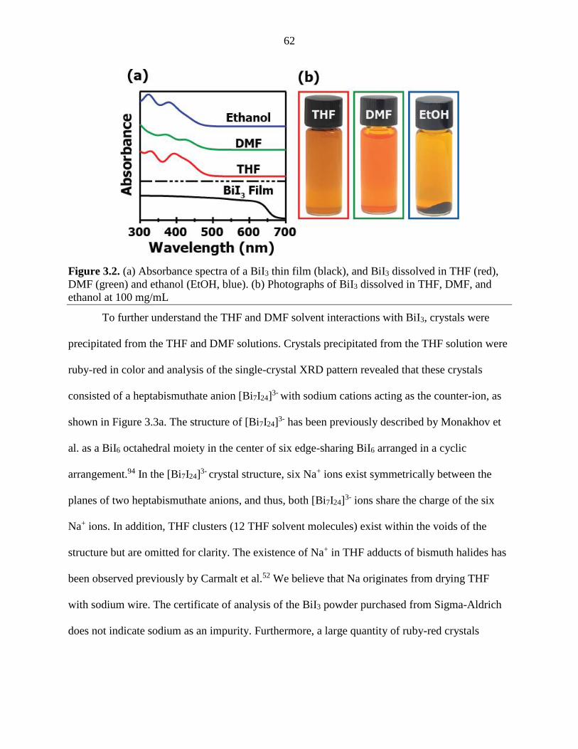
62
Figure 3.2. (a) Absorbance spectra of a BiI3 thin film (black), and BiI3 dissolved in THF (red),
DMF (green) and ethanol (EtOH, blue). (b) Photographs of BiI3 dissolved in THF, DMF, and
ethanol at 100 mg/mL
To further understand the THF and DMF solvent interactions with BiI3, crystals were
precipitated from the THF and DMF solutions. Crystals precipitated from the THF solution were
ruby-red in color and analysis of the single-crystal XRD pattern revealed that these crystals
consisted of a heptabismuthate anion [Bi7I24]3- with sodium cations acting as the counter-ion, as
shown in Figure 3.3a. The structure of [Bi7I24]3- has been previously described by Monakhov et
al. as a BiI6 octahedral moiety in the center of six edge-sharing BiI6 arranged in a cyclic
arrangement.94 In the [Bi7I24]3- crystal structure, six Na+ ions exist symmetrically between the
planes of two heptabismuthate anions, and thus, both [Bi7I24]3- ions share the charge of the six
Na+ ions. In addition, THF clusters (12 THF solvent molecules) exist within the voids of the
structure but are omitted for clarity. The existence of Na+ in THF adducts of bismuth halides has
been observed previously by Carmalt et al.52 We believe that Na originates from drying THF
with sodium wire. The certificate of analysis of the BiI3 powder purchased from Sigma-Aldrich
does not indicate sodium as an impurity. Furthermore, a large quantity of ruby-red crystals

63
(which contain sodium) was obtained during crystallization. This implies that the Na is more
than just a trace impurity, and THF is likely the Na source.
Orange prismatic crystals were isolated by precipitating BiI3 dissolved in DMF. Based on
single-crystal XRD, we found that these crystals are composed of two distinct structures that
exhibit salt-like characteristics; that is, the primitive cell is composed of a cationic structure and
anionic structure, as illustrated in Figure 3.3b. The first structure is a Bi3+ cation solvated by the
oxygen atoms of eight DMF molecules, and the second structure is a trinuclear iodobismuthate
anion [Bi3I12]3-. The charge of the BiI3+ atom is balanced by the charge of the anionic
iodobismuthate molecule. All of the precipitated crystals were unstable upon removing them
from the liquid environment; upon doing so, they decompose into BiI3. This decomposition is
similar to what Carmalt et al. reported in their study of THF adducts of bismuth trihalides.52 To
prevent decomposition, we covered the crystals with Paratone® oil during single crystal XRD
analysis. The crystal system of the BiI3 complex isolated from THF is trigonal, while the crystal
system obtained from the DMF solution is monoclinic.
Figure 3.3. Unit cells of BiI3 complexes with (a) THF and (b) DMF solvent.

64
We used spin coating to deposit thin-films from the BiI3 solutions in THF. THF was
chosen as the solvent because it was used as the solvent in the development of the first BiI3 thin-
film PV device by Lehner et al.42 and we first wanted to reproduce their work. Other solvents —
such as DMF — can also be used in the processing of BiI3 thin-films. A 100 mg/mL solution of
BiI3 in THF was spin coated inside a N2-filled glovebox, resulting in an approximately 200 nm
thick film of BiI3, as measured by atomic force microscopy (AFM). Spin coating with
concentrations greater than 100 mg/mL resulted in cracking of the film. This is due to the high
vapor pressure of THF solvent; when using higher concentrations, the rapid evaporation of the
solvent results in the breaking of the film. The cracks in the thin-film are more visible using
higher concentrations as compared to using concentrations < 100 mg/mL, but presumably still
exist with lower concentrations. A thickness versus concentration profile can be found in Figure
3.4a. The thickness of the film was measured by applying a thin scratch on the film with a
syringe needle. The difference in height between the valley of the scratch and the film is taken as
the thickness. Since only one layer of BiI3 can be deposited (additional deposition of BiI3 results
in the former layer being dissolved), the thickness of BiI3 can be varied by the concentration of
BiI3 in solution.
Transmittance measurements of a 200 nm thick film resulted in ~90% absorption at 2.0
eV (Figure 3.4b). Using Tauc analysis and assuming an indirect bandgap, the bandgap of BiI3
was evaluated to be ~1.83 eV (Figure 3.5) which is slightly larger than the value presented by
Brandt et al.41 and Lehner et al.42 The absorption coefficient (a) was calculated using Equation
3.1 from the transmittance (T), reflectance (R), and thin film thickness (d) measurements. We
assumed an indirect bandgap and plotted (ahν)0.5 versus hν.54 The bandgap was found by finding
the intersection of the linear absorption edge with the sub bandgap absorption.55 We measured
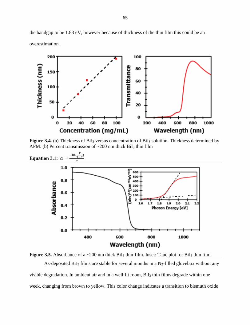
65
the bandgap to be 1.83 eV, however because of thickness of the thin film this could be an
overestimation.
Figure 3.4. (a) Thickness of BiI3 versus concentration of BiI3 solution. Thickness determined by
AFM. (b) Percent transmission of ~200 nm thick BiI3 thin film
Equation 3.1: 𝑎 =−ln(
𝑇
1−𝑅)
𝑑
Figure 3.5. Absorbance of a ~200 nm thick BiI3 thin-film. Inset: Tauc plot for BiI3 thin film.
As-deposited BiI3 films are stable for several months in a N2-filled glovebox without any
visible degradation. In ambient air and in a well-lit room, BiI3 thin films degrade within one
week, changing from brown to yellow. This color change indicates a transition to bismuth oxide

66
(Bi2O3). However, BiI3 stored in the dark (in ambient air) are stable for at least several months.
This suggests that BiI3 stability is affected more by light rather than air. Further studies are
needed to thoroughly assess the photo-thermal and environmental stability of BiI3.
When spin coating BiI3 dissolved in THF, the films transitioned from orange to black,
indicating a decomposition of the heptabismuthate-THF complex into BiI3. When spin coating
BiI3 films co-dissolved in THF and hydroiodic acid (HI), or dissolved in DMF, the film remained
orange even after spin coating, indicating that these intermediate complexes are more stable
(Figure 3.6). Addition of HI to the precursor was initially investigated because Lehner et al.
included HI in their BiI3 device studies.42 In our study, HI was added in a 1:1 molar ratio with
BiI3, resulting in a change in color of the solution from light orange to dark red-purple. This red-
purple color is consistent with the formation of polytetrahydrofuran, which can form in the
presence of strong acids.56 Upon heating at 100 °C or storing at room temperature overnight, the
films decomposed into BiI3.
Figure 3.6. Photographs of BiI3 thin films deposited with (a) THF as coordinating solvent or (b)
DMF as coordinating solvent after spin coating. Adding HI to THF resulted in a film like (b).
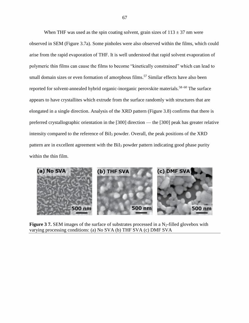
67
When THF was used as the spin coating solvent, grain sizes of 113 ± 37 nm were
observed in SEM (Figure 3.7a). Some pinholes were also observed within the films, which could
arise from the rapid evaporation of THF. It is well understood that rapid solvent evaporation of
polymeric thin films can cause the films to become “kinetically constrained” which can lead to
small domain sizes or even formation of amorphous films.57 Similar effects have also been
reported for solvent-annealed hybrid organic-inorganic perovskite materials.58–60 The surface
appears to have crystallites which extrude from the surface randomly with structures that are
elongated in a single direction. Analysis of the XRD pattern (Figure 3.8) confirms that there is
preferred crystallographic orientation in the [300] direction — the [300] peak has greater relative
intensity compared to the reference of BiI3 powder. Overall, the peak positions of the XRD
pattern are in excellent agreement with the BiI3 powder pattern indicating good phase purity
within the thin film.
Figure 3 7. SEM images of the surface of substrates processed in a N2-filled glovebox with
varying processing conditions: (a) No SVA (b) THF SVA (c) DMF SVA

68
Figure 3 8. XRD of BiI3 thin films processed in a N2-filled glovebox with varied SVA
conditions.
We explored solvent vapor annealing (SVA) as a method to promote grain growth and
improve film quality. Xiao et al. recently demonstrated SVA as a method to improve film
quality, increase grain size, and improve carrier diffusion lengths in methylammonium lead
iodide perovskite thin-film PVs.61 Furthermore, SVA has been a widely used strategy for
enhancing charge carrier transport and modifying grain morphology in polymeric and organic
semiconductors.62–64 In our study, BiI3 thin films were exposed to controlled amounts of a
solvent vapor at a controlled temperature.
We studied the effects of exposing spin coated BiI3 thin films to THF and DMF solvent
vapor in an inert (N2) environment. SVA with THF and with DMF were found to increase the
grain size of BiI3 thin films. By measuring domain sizes of plan-view SEM, we were able to
quantify the effect of SVA on the surface. THF SVA led to a wide dispersity in grain sizes from
a maximum size of 315 nm to a minimum size of 36 nm (Figure 3.7b). The THF also appeared to
be embedded within a matrix, which may consist of fine-grained or amorphous materials. This is

69
corroborated by XRD (Figure 3.8), which showed weaker intensity. The average grain size of
THF SVA films was 127 ± 76 nm. On average, this was only slightly larger compared to films
without any SVA treatment; however, there was a much broader grain size distribution and a
more isotropic morphology for THF SVA thin films. The polydispersity in grain size after THF
SVA suggests Ostwald ripening; that is, larger grains grow at the expense of smaller grains. SVA
in a DMF environment resulted in a much different morphology and substantially larger grain
sizes compared to no SVA and THF SVA. A maximum size of 2.5 µm and a minimum size of
122 nm on the surface were measured (Figure 3.9 and Figure 3.7c). The larger grain size after
DMF SVA indicates DMF vapor facilitates the migration of BiI3 and promotes grain growth.
However, there are large gaps (0.08 ± 0.05 µm2) throughout the film, presumably arising from
the coalescence of the BiI3 to form larger grains. The XRD pattern of the BiI3 thin film after
DMF SVA is also in excellent agreement with the XRD pattern of the BiI3 powder. The peak
intensities become similar to those of the BiI3 powder reference, implying that the BiI3 grains
recrystallize and become randomly oriented after DMF SVA. In contrast, the films with THF
SVA retained preferred orientation in the [300] direction.
Figure 3.9. SEM image of BiI3 thin films processed with DMF solvent vapor at (a) 5,000x
magnification and (b) 15,000x magnification.

70
To evaluate the BiI3 thin films for PV application, we fabricated proof-of-concept PV
devices with a superstrate configuration (Glass/FTO/TiO2/BiI3/V2O5/Au), as illustrated in Figure
3.10. The TiO2 and BiI3 are processed via solution-based deposition, while V2O5 and Au are
deposited via high vacuum thermal vapor deposition. We found that thin film PV devices
processed in a N2-filled glovebox had lower open-circuit voltage (VOC) compared to devices
where the BiI3 layer was processed in air (Figure 3.11b). We hypothesize that processing the BiI3
layer in air creates a thin layer of oxidized material, BiOI, at the surface which facilitates hole
extraction at the BiI3/V2O5 interface.
Figure 3.10. Schematic of the device structure and SEM cross-section.
XPS confirmed the existence of oxidized Bi on the surface (Figure 3.11a) and depth
profiling (Figure 3.12) indicated that the oxidation only existed at the surface. Depth-profiling
XPS was used to estimate the maximum possible thickness of the BiOI layer. An upper limit was
established by observing the point at which the oxygen signal approaches 0%. The lower limit
was taken as the first valid data point of the depth-profiling after the sputtering process had
begun (37 nm). Low resolution prevented greater precision in determining the thickness. To
convert etch time into a thickness, the BiI3 film was estimated to be 200 nm thick and the
interface between the BiI3 film and the silicon substrate was assumed to occur at the crossover
between the iodine 3d and silicon 2s atomic percent. This occurred at 41.5 seconds, the etch rate

71
was estimated at 4.6 nm/s. From depth-profiling we conclude that the thickness of the BiOI layer
is ~37 nm thick.
Figure 3.11. (a) X-ray photoelectron spectroscopy of thin films processed in a N2-filled
glovebox and in ambient air. (b) J-V characteristics of BiI3 PVs processed in a N2-filled glovebox
and in ambient air.
Figure 3.12. Atomic percentage of elements in BiI3 film as a function of etch time.

72
By more aggressively oxidizing the material we are able to show the existence of BiOI
with grazing incidence x-ray diffraction measurements (Figure 3.13). We hypothesize that the
BiOI surface layer facilitates charge transport between BiI3 and the HTL V2O5. BiOI is a p-type
semiconductor with a valence band maximum of ~ -6.8 eV vs. vacuum, making it suitable for
hole extraction from many semiconductors.65 In the absence of Fermi pinning, many transition
metal oxide HTLs with deep work functions such as MoO3 or V2O5 should provide sufficient
driving force to extract photogenerated holes from BiI3; i.e., they should form a favorable
contact.66 However, the VOC for N2-processed devices is low, (< 75 mV) implying that Fermi
level pinning could occur at the BiI3/metal oxide interface, limiting the VOC. From this evidence,
we infer that the BiOI layer improves the interfacial defect density by reducing Fermi level
pinning, thus improving the VOC.
Figure 3.13. Grazing incidence x-ray diffraction of oxidized BiI3 showing the formation of BiOI.
Further oxidation of the material results in the film changing into a yellow color indicating the
formation of Bi2O3.

73
Processing in air also led to a different film morphology compared to processing in N2.
Plan-view SEM of BiI3 thin films processed in air without any SVA (Figure 3.14) shows uniform
surface coverage compared to processing in N2. However, there are multiple pinholes in the film
— presumably due to rapid evaporation of the THF solvent during spin coating. Given that
processing in air resulted in improved PV device performance, we investigated SVA in ambient
air. We found the result of SVA in air to be different compared to SVA in N2.
Figure 3.14. Plan-view SEM images BiI3 thin films processed without SVA a) in N2 and b) in air
THF SVA in air resulted in drastically different film morphology compared to SVA in N2
(Figure 3.15). The grain shape is rod-like compared to more rounded features in N2-processing.
Grain sizes on average from air processing are smaller than processing in N2. DMF SVA in air
resulted in uniform coverage (Figure 3.16), which is in contrast to DMF SVA in N2, which
resulted in film dewetting. The grain shape appears similar in both cases, and is more rounded
and isotropic compared to films with THF SVA and no SVA treatment. However, the grains are
smaller on average when processed in air, compared to those processed in N2.

74
Figure 3.15. Plan-view SEM images BiI3 thin films processed with THF SVA a) in N2 and b) in
air
Figure 3.16. Plan-view SEM images BiI3 thin films processed with DMF SVA a) in N2 and b) in
air
The difference in the morphologies for THF and DMF SVA films processed in air vs. N2
could arise from a number of factors. For instance, in N2 the grains may grow rapidly to
minimize interfacial area; while in air, the thin surface oxide layer that forms could stabilizes
smaller grain sizes. Overall, DMF SVA in air resulted in continuous films with relatively
monodisperse grains that extended from the surface to the substrate, as observed in cross-
sectional SEM (Figure 3.17). The difference between THF SVA and no SVA in air is minimal
(Figure 3.18). This may be partially due to the processing temperature. The boiling point for
THF is 66 °C, so higher temperatures (>100 °C) would result in THF vapor remaining in the

75
vapor phase and not diffusing into the thin film. The BiOI may also prevent THF diffusion, thus
resulting in minimal change when exposed to THF solvent vapor. DMF, on the other hand, has a
boiling point of 153 °C, so it is assumed that processing at 100 °C is more favorable for DMF
solvent vapors to condense and diffuse into the material.
Figure 3.17. Cross sectional SEM images with TLD detector of (a) No SVA BiI3 PV device, and
(b) DMF SVA BiI3 PV device both processed in air. Note the smaller grains located in the no
SVA.
Figure 3.18. Plan-view SEM images BiI3 thin films processed in air with a) No SVA b) THF
SVA c) DMF SVA
We fabricated PV devices using BiI3 thin films that were completely processed in air
(spin coated and SVA in air). J-V characteristics of these devices under AM1.5 illumination can
be found in Figure 3.19 for different SVA conditions. The short-circuit current (JSC) of BiI3 PVs
processed without SVA is strongly dependent on annealing temperature, with an optimal
temperature of 165 °C (Figure 3.20a). However, temperatures greater than 165 °C resulted in the

76
visible degradation of the BiI3 material during processing. In fact, prolonged exposure to
temperatures greater than 150 °C (~6 hours) also resulted in degradation.
Figure 3.19. J−V characteristics under AM1.5 illumination of BiI3 thin films processed without
SVA (black), with THF SVA (blue), and with DMF SVA (green).
We observed a maximum JSC at 100 °C for devices fabricated with DMF SVA (Figure
3.20b). Temperatures less than 100 °C presumably caused excessive solvent to diffuse into the
film, causing partial or complete dissolution (which we observed visually with SVA
temperatures ≥ 80 °C). Prolonged exposure to DMF solvent vapor (> 10 minutes) did not
significantly change the JSC. In a similar study, Xiao et al. demonstrated the effect of prolonged
exposure to solvent vapors on perovskite thin films.61 In their study, rapid grain growth was
observed within the first 20 minutes of solvent vapor annealing with minimal grain growth
afterwards. Typically, an increase in grain size accompanies an increase in the current density of
the PV device due to a reduction of grain boundaries. Since the JSC does not change significantly

77
after 10 minutes of SVA, we conclude that the crystal grains reach a near maximum size after a
short exposure time to DMF solvent vapors.
Figure 3.20 (a) The effect of varying the processing temperature on the JSC of BiI3 thin films
without SVA. (b) The effect of varying the DMF SVA temperature on the JSC of BiI3 PV
devices.
We observed that SVA treatment improves PV device performance. DMF SVA had a
large improvement in the JSC with a value of 5.0 ± 0.9 (mA/cm2) with 34 measured devices —
more than a three-fold improvement over both THF SVA (1.6 ± 0.4 mA/cm2) and no SVA (1.23
± 0.2 mA/cm2) with 23 and 26 devices measured, respectively. The improvement in JSC was
accompanied by a decrease in the fill factor (FF) for DMF SVA devices, thus signifying a
decrease of the shunt resistance with increased grain size. Devices without SVA had a FF of 35.5
± 0.2 while THF and DMF SVA films had FFs of 33.4 ± 3.7 and 29.9 ± 2.4, respectively. A
champion device with PCE of just over 1.0% was achieved using DMF SVA. (Figure 3.21)

78
Figure 3.21. The effect of post deposition annealing. Champion device IV sweep parameters: JSC
(7.0 mA/cm2), VOC (364 mV), FF (39.2%), and PCE (1.02%). The device was processed with
DMF solvent vapors at 100 °C for ten minutes and thermal annealed at 100 °C for ten minutes.
We used external quantum efficiency (EQE) to quantify photogenerated charge carrier
extraction in the BiI3 devices (Figure 3.22a). The DMF SVA devices show much higher EQE
compared to the THF SVA and without SVA treatment devices. As expected, this follows the
trend of JSC values obtained for these treatments. From analyzing the spectral dependence of
EQE, it is seen that there is a relatively poor extraction of higher-energy photons. This implies a
loss in photogenerated carrier extraction efficiency for higher-energy photons preferentially
absorbed near the TiO2/BiI3 interface relative to the remainder of the device — arising from a
recombination of electron-hole pairs at defect states near this interface. The EQE suggests a need
to evaluate more suitable n-type heterojunction partners in order to improve the PCE of BiI3 PV
devices. A possible strategy to overcome the low electron collection at the BiI3/TiO2 interface is
to use a CdS buffer layer in-between BiI3 and TiO2. A CdS buffer layer has been shown to
reduce surface recombination for CIGS PVs.67,68

79
Figure 3. 22. (a) External quantum efficiency (EQE) of BiI3 thin films processed without SVA
(black), with THF SVA (blue), and with DMF SVA (green). (b) Steady-state photoluminescence
(PL) spectra of BiI3 processed without SVA (black), with THF SVA (blue), and with DMF SVA
(green). PL spectra are normalized to the film absorbance at the excitation wavelength (532 nm).
(c) Photoluminescence lifetime of BiI3 processed in N2 (red), and in air (blue); the instrumental
response function (obtained from a substrate without a BiI3 film using filter that only transmits
the excitation light) is shown in black.
We measured PL and PL lifetime to gain insight on how different treatments affect the
excited state dynamics (Figure 3.22b). PL was normalized to the film absorbance (Figure 3.23c)
at excitation wavelength (532 nm) to remove the effect of variation in film thickness and
possible change in absorption cross-section due to heterogeneity. SVA did not have a significant
effect on the PL intensity or position, nor was there effect on carrier lifetimes (Figure 3.24).
Given the improved device performance with DMF SVA, it was initially surprising to us that
there is no change in carrier lifetime. However, this agrees with a report by Brandt et al.41, who
observed no difference in carrier lifetime between spin coated and physical vapor transport
deposited BiI3 thin films which are most likely to differ in morphology. Thus, this implies that
the improvement in JSC and device efficiency after DMF SVA arises from increased charge
carrier mobility, rather than lifetime, within the active layer. The higher mobility is likely due to
the fact that the grains extend the thickness of the absorber layer, reducing transport across BiI3
grain boundaries.

80
Figure 3.23. The effect of processing conditions on device (a) transmittance, (b) reflectance, and
(c) absorbance on BiI3 thin films.
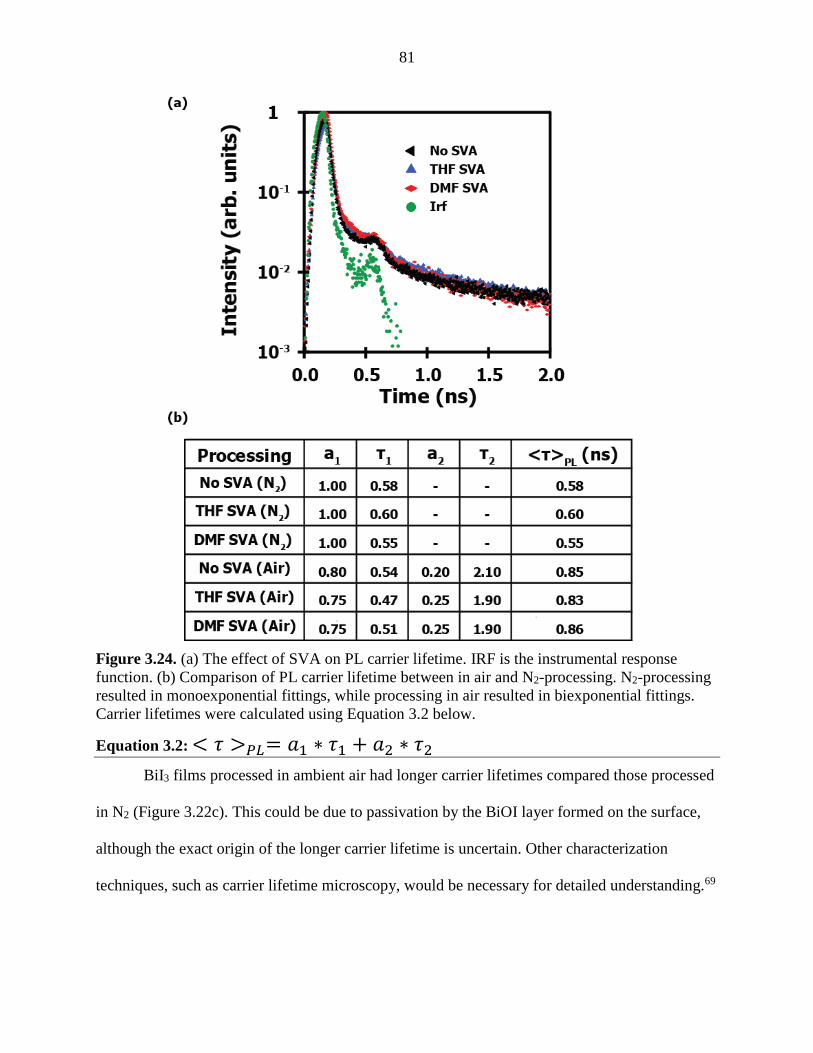
81
Figure 3.24. (a) The effect of SVA on PL carrier lifetime. IRF is the instrumental response
function. (b) Comparison of PL carrier lifetime between in air and N2-processing. N2-processing
resulted in monoexponential fittings, while processing in air resulted in biexponential fittings.
Carrier lifetimes were calculated using Equation 3.2 below.
Equation 3.2: < 𝜏 >𝑃𝐿= 𝑎1 ∗ 𝜏1 + 𝑎2 ∗ 𝜏2
BiI3 films processed in ambient air had longer carrier lifetimes compared those processed
in N2 (Figure 3.22c). This could be due to passivation by the BiOI layer formed on the surface,
although the exact origin of the longer carrier lifetime is uncertain. Other characterization
techniques, such as carrier lifetime microscopy, would be necessary for detailed understanding.69

82
Considering the relatively wide-bandgap of BiI3, the PV devices reported here exhibit
much lower VOC values than expected (i.e., large VOC deficit). In order to improve the VOC, there
is evidence that the device architecture might need to be modified — specifically the electron
and hole-extracting interfaces. As mentioned above, EQE indicated poor collection of charge
carriers that were generated near the p-n interface, implying that carrier recombination is higher
at this interface. Because VOC is proportional to the ratio of dark and light current, the increased
recombination is at least one source of the low VOC. Although the best BiI3 PV devices shown
here have much higher PCE, those reported by Lehner et al.42 had higher VOC (>400 mV) values.
In their study, they used a poly-indacenodithiophenedifluoro-benzothiadiazole (PIDT-DFBT)
HTL, which had higher VOC values compared to using a poly-triarylamine (PTAA) HTL (VOC =
220 mV). The authors attributed this to the fact that PIDT-DFBT has a deeper valence band
maximum compared to PTAA.42 In our study, MoO3 was initially chosen as the HTL because of
its very deep work function (φ = -6.7 eV, vs. vacuum).70 However, devices with a V2O5 (φ =-5.6
eV)71 HTL resulted in higher VOC values compared to MoO3 (Figure 3.25). This indicates
possible chemical incompatibles between BiI3 and MoO3. As discussed previously, we
hypothesize that Fermi pinning occurs at the BiI3/HTL interface. Understanding hole extraction
will be a critical aspect to improving the PCE of BiI3 PVs. Band positions of the entire device
architecture, including MoO3 can be found in Figure 3.26.

83
Figure 3.25. The effect of varying metal oxide hole transport layers for BiI3 PV devices. BiI3
was also found to be incompatible with Ag — using Ag as the top contact of PV devices resulted
in the diffusion of BiI3 into the metal contact. Au was used instead because it was chemically
compatible with BiI3.
Figure 3.26. Energy band diagram of the materials used in the study. Band levels of TiO2,72
BiI3,42 BiOI,65 V2O5,
70 and MoO373 were all found in the literature.

84
3.5. Summary and Conclusions
In summary, we demonstrated that BiI3 forms molecular complexes with coordinating
solvents such as THF and DMF, enabling solution-based processing of BiI3 thin films. Molecular
complexes have been used widely over the past decade in “dimension reduction” approaches;74
however, in most cases dimensional reduction requires the use of a relatively corrosive
(reducing) solvent to solubilize the inorganic material. In this case, BiI3 readily forms complexes
with relatively benign solvents in a similar manner to PbI2 — but unlike PbI2, the bandgap of
BiI3 is suitable for use as a PV absorber layer. Overall, processing in air provided multiple
benefits to improving the PCE of BiI3 thin film PVs: a BiOI layer forms at the surface that
facilitates hole extraction, and this surface layer also presumably prevents film dewetting during
solvent vapor annealing in DMF. Annealing in solvent vapor was found to increase grain size
and reduce film porosity, especially in the case of DMF vapor. Based on photoluminescence
spectroscopy, we can infer that the improved performance is due to improved carrier mobility,
since the excited-state lifetime does not increase after SVA. In non-optimized, all-inorganic PV
devices, we achieved 1.0% PCE, which is the highest reported efficiency for this material, and
the first report of an all-inorganic BiI3 PV device structure. This demonstrates the potential of
BiI3 as a potential non-toxic alternative to hybrid perovskite materials that has improved air-
stability.
3.6. Acknowledgments
The authors thank Dr. Curtis Mosher for assistance with AFM measurements, Dr. Matt
Besser for assistance in acquiring XRD measurements, Dr. Arkady Ellern and the Molecular
Structure Laboratory of Iowa State University for measuring single crystal XRD, and Kurt Koch
of Ames Laboratory for assisting in cross-sectional SEM of thin films. RDN acknowledges
support from the Catron foundation. This work was supported in part by the U.S. Department of

85
Energy, Office of Science, and Office of Workforce Development for Teachers and Scientists
(WDTS) under the Science Undergraduate Laboratory Internship (SULI) program. Finally, this
research is supported by the U.S. Department of Energy, Office of Basic Energy Sciences,
Division of Chemical Sciences, Geosciences, and Biosciences through the Ames Laboratory. The
Ames Laboratory is operated for the U.S. Department of Energy by Iowa State University under
Contract No. DE-AC02-07CH11358.
3.7. References
1. Gur, I., Fromer, N. A., Geier, M. L. & Alivisatos, A. P. Air-Stable All-Inorganic Nanocrystal
Solar Cells Processed from Solution. Science 310, 462 (2005).
2. Graetzel, M., Janssen, R. A. J., Mitzi, D. B. & Sargent, E. H. Materials interface engineering
for solution-processed photovoltaics. Nature 488, 304 (2012).
3. Milliron, D. J., Mitzi, D. B., Copel, M. & Murray, C. E. Solution-Processed Metal
Chalcogenide Films for p-Type Transistors. Chem. Mater. 18, 587–590 (2006).
4. Panthani, M. G. et al. Synthesis of CuInS2, CuInSe2, and Cu(InxGa1-x)Se2 (CIGS)
Nanocrystal ‘Inks’ for Printable Photovoltaics. J. Am. Chem. Soc. 130, 16770–16777 (2008).
5. Shirasaki, Y., Supran, G. J., Bawendi, M. G. & Bulović, V. Emergence of colloidal quantum-
dot light-emitting technologies. Nat. Photonics 7, 13 (2012).
6. Liu, C. et al. Ultrasensitive solution-processed broad-band photodetectors using
CH3NH3PbI3 perovskite hybrids and PbS quantum dots as light harvesters. Nanoscale 7,
16460–16469 (2015).
7. McDonald, S. A. et al. Solution-processed PbS quantum dot infrared photodetectors and
photovoltaics. Nat. Mater. 4, 138 (2005).
8. Nozik, A. J. Making the most of photons. Nat. Nanotechnol. 4, 548 (2009).
9. Akhavan, V. A. et al. Influence of Composition on the Performance of Sintered
Cu(In,Ga)Se2 Nanocrystal Thin-Film Photovoltaic Devices. ChemSusChem 6, 481–486
(2013).
10. Guo, Q., Ford, G. M., Hillhouse, H. W. & Agrawal, R. Sulfide Nanocrystal Inks for Dense
Cu(In1−xGax)(S1−ySey)2 Absorber Films and Their Photovoltaic Performance. Nano Lett.
9, 3060–3065 (2009).

86
11. Jasieniak, J., MacDonald, B. I., Watkins, S. E. & Mulvaney, P. Solution-Processed Sintered
Nanocrystal Solar Cells via Layer-by-Layer Assembly. Nano Lett. 11, 2856–2864 (2011).
12. Panthani, M. G. et al. High Efficiency Solution Processed Sintered CdTe Nanocrystal Solar
Cells: The Role of Interfaces. Nano Lett. 14, 670–675 (2014).
13. Crisp, R. W. et al. Nanocrystal Grain Growth and Device Architectures for High-Efficiency
CdTe Ink-Based Photovoltaics. ACS Nano 8, 9063–9072 (2014).
14. Bag, S. et al. Low band gap liquid-processed CZTSe solar cell with 10.1% efficiency.
Energy Env. Sci 5, 7060–7065 (2012).
15. Jiang, C., Liu, W. & Talapin, D. V. Role of Precursor Reactivity in Crystallization of
Solution-Processed Semiconductors: The Case of Cu2ZnSnS4. Chem. Mater. 26, 4038–4043
(2014).
16. Jiang, C., Lee, J.-S. & Talapin, D. V. Soluble Precursors for CuInSe2, CuIn1–xGaxSe2, and
Cu2ZnSn(S,Se)4 Based on Colloidal Nanocrystals and Molecular Metal Chalcogenide
Surface Ligands. J. Am. Chem. Soc. 134, 5010–5013 (2012).
17. Luther, J. M. et al. Schottky Solar Cells Based on Colloidal Nanocrystal Films. Nano Lett. 8,
3488–3492 (2008).
18. Ip, A. H. et al. Hybrid passivated colloidal quantum dot solids. Nat. Nanotechnol. 7, 577
(2012).
19. Chuang, C.-H. M., Brown, P. R., Bulović, V. & Bawendi, M. G. Improved performance and
stability in quantum dot solar cells through band alignment engineering. Nat Mater 13, 796–
801 (2014).
20. Best Research-Cell Efficiencies.
21. Wang, Q. et al. Large fill-factor bilayer iodine perovskite solar cells fabricated by a low-
temperature solution-process. Energy Env. Sci 7, 2359–2365 (2014).
22. Sun, K. et al. The role of solvent vapor annealing in highly efficient air-processed small
molecule solar cells. J Mater Chem A 2, 9048–9054 (2014).
23. Choi, J. J., Yang, X., Norman, Z. M., Billinge, S. J. L. & Owen, J. S. Structure of
Methylammonium Lead Iodide Within Mesoporous Titanium Dioxide: Active Material in
High-Performance Perovskite Solar Cells. Nano Lett. 14, 127–133 (2014).
24. Heo, J. H. et al. Efficient inorganic–organic hybrid heterojunction solar cells containing
perovskite compound and polymeric hole conductors. Nat. Photonics 7, 486 (2013).

87
25. Babayigit, A., Ethirajan, A., Muller, M. & Conings, B. Toxicity of organometal halide
perovskite solar cells. Nat. Mater. 15, 247 (2016).
26. Müller, C. et al. Water Infiltration in Methylammonium Lead Iodide Perovskite: Fast and
Inconspicuous. Chem. Mater. 27, 7835–7841 (2015).
27. Christians, J. A., Miranda Herrera, P. A. & Kamat, P. V. Transformation of the Excited State
and Photovoltaic Efficiency of CH3NH3PbI3 Perovskite upon Controlled Exposure to
Humidified Air. J. Am. Chem. Soc. 137, 1530–1538 (2015).
28. Dualeh, A., Gao, P., Seok, S. I., Nazeeruddin, M. K. & Grätzel, M. Thermal Behavior of
Methylammonium Lead-Trihalide Perovskite Photovoltaic Light Harvesters. Chem. Mater.
26, 6160–6164 (2014).
29. Hao, F., Stoumpos, C. C., Cao, D. H., Chang, R. P. H. & Kanatzidis, M. G. Lead-free solid-
state organic-inorganic halide perovskite solar cells. Nat Photon 8, 489–494 (2014).
30. Stoumpos, C. C., Malliakas, C. D. & Kanatzidis, M. G. Semiconducting Tin and Lead Iodide
Perovskites with Organic Cations: Phase Transitions, High Mobilities, and Near-Infrared
Photoluminescent Properties. Inorg. Chem. 52, 9019–9038 (2013).
31. Eckhardt, K. et al. Crystallographic insights into (CH3NH3)3(Bi2I9): a new lead-free hybrid
organic-inorganic material as a potential absorber for photovoltaics. Chem Commun 52,
3058–3060 (2016).
32. Öz, S. et al. Zero-dimensional (CH3NH3)3Bi2I9 perovskite for optoelectronic applications.
Nanotechnol. Gener. High Effic. Photovolt. NEXTGEN NANOPV Spring Int. Sch. Workshop
158, 195–201 (2016).
33. Singh, T., Kulkarni, A., Ikegami, M. & Miyasaka, T. Effect of Electron Transporting Layer
on Bismuth-Based Lead-Free Perovskite (CH3NH3)3 Bi2I9 for Photovoltaic Applications.
ACS Appl. Mater. Interfaces 8, 14542–14547 (2016).
34. Saparov, B. et al. Thin-Film Preparation and Characterization of Cs3Sb2I9: A Lead-Free
Layered Perovskite Semiconductor. Chem. Mater. 27, 5622–5632 (2015).
35. Park, B.-W. et al. Bismuth Based Hybrid Perovskites A3Bi2I9 (A: Methylammonium or
Cesium) for Solar Cell Application. Adv. Mater. 27, 6806–6813 (2015).
36. Cotton, A. F., Wilkinson, G., Bochmann, M. & Murillo, C. A. Advanced inorganic
chemistry. (Wiley, 1999).
37. Sidgwick, N. V. The electronic theory of valency. (1929).
38. Nason, D. & Keller, L. The growth and crystallography of bismuth tri-iodide crystals grown
by vapor transport. J. Cryst. Growth 156, 221–226 (1995).
88
39. Mackay, R. A. & Henderson, W. Introduction to modern inorganic chemistry. (CRC Press,
2002).
40. Podraza, N. J. et al. Band gap and structure of single crystal BiI3: Resolving discrepancies in
literature. J. Appl. Phys. 114, 033110 (2013).
41. Brandt, R. E. et al. Investigation of Bismuth Triiodide (BiI3) for Photovoltaic Applications.
J. Phys. Chem. Lett. 6, 4297–4302 (2015).
42. Lehner, A. J. et al. Electronic structure and photovoltaic application of BiI3. Appl. Phys.
Lett. 107, 131109 (2015).
43. Lintereur, A. T., Qiu, W., Nino, J. C. & Baciak, J. Characterization of bismuth tri-iodide
single crystals for wide band-gap semiconductor radiation detectors. Symp. Radiat. Meas.
Appl. SORMA XII 2010 652, 166–169 (2011).
44. Fabian, D. M. & Ardo, S. Hybrid organic-inorganic solar cells based on bismuth iodide and
1,6-hexanediammonium dication. J Mater Chem A 4, 6837–6841 (2016).
45. Persson, C. et al. Optical Absorption of Large Band-Gap SbxBi1-xI3 Alloys. MRS Proc.
744, (2002).
46. Boopathi, K. M. et al. Solution-processable bismuth iodide nanosheets as hole transport
layers for organic solar cells. Sol. Energy Mater. Sol. Cells 121, 35–41 (2014).
47. Green, M. A. & Keevers, M. J. Optical properties of intrinsic silicon at 300 K. Prog.
Photovolt. Res. Appl. 3, 189–192 (1995).
48. Blakemore, J. S. Semiconducting and other major properties of gallium arsenide. J. Appl.
Phys. 53, R123–R181 (1982).
49. Bhattacharjee, U. et al. Fluorescence Spectroscopy of the Retina for the Screening of Bovine
Spongiform Encephalopathy. J. Agric. Food Chem. 64, 320–325 (2016).
50. Sainz, M. et al. Plant hemoglobins may be maintained in functional form by reduced flavins
in the nuclei, and confer differential tolerance to nitro-oxidative stress. Plant J. 76, 875–887
(2013).
51. Bhattacharjee, U., Beck, C., Winter, A., Wells, C. & Petrich, J. W. Tryptophan and ATTO
590: Mutual Fluorescence Quenching and Exciplex Formation. J. Phys. Chem. B 118, 8471–
8477 (2014).
52. Carmalt, C. J. et al. Tetrahydrofuran Adducts of Bismuth Trichloride and Bismuth
Tribromide. Inorg. Chem. 35, 3709–3712 (1996).

89
53. Johansson, M. B., Zhu, H. & Johansson, E. M. J. Extended Photo-Conversion Spectrum in
Low-Toxic Bismuth Halide Perovskite Solar Cells. J. Phys. Chem. Lett. 7, 3467–3471
(2016).
54. Tauc, J., Grigorovici, R. & Vancu, A. Optical Properties and Electronic Structure of
Amorphous Germanium. Phys. Status Solidi B 15, 627–637 (1966).
55. Chen, Z. et al. Accelerating materials development for photoelectrochemical hydrogen
production: Standards for methods, definitions, and reporting protocols. J. Mater. Res. 25, 3–
16 (2010).
56. Pruckmayr, G., Dreyfuss, P. & Dreyfuss, M. P. Polyethers, Tetrahydrofuran and Oxetane
Polymers. in Kirk-Othmer Encyclopedia of Chemical Technology (John Wiley & Sons, Inc.,
2000). doi:10.1002/0471238961.2005201816182103.a01
57. Sinturel, C., Vayer, M., Morris, M. & Hillmyer, M. A. Solvent Vapor Annealing of Block
Polymer Thin Films. Macromolecules 46, 5399–5415 (2013).
58. Moore, D. T. et al. Crystallization Kinetics of Organic–Inorganic Trihalide Perovskites and
the Role of the Lead Anion in Crystal Growth. J. Am. Chem. Soc. 137, 2350–2358 (2015).
59. Liang, P.-W. et al. Additive Enhanced Crystallization of Solution-Processed Perovskite for
Highly Efficient Planar-Heterojunction Solar Cells. Adv. Mater. 26, 3748–3754 (2014).
60. Chen, Q. et al. Planar Heterojunction Perovskite Solar Cells via Vapor-Assisted Solution
Process. J. Am. Chem. Soc. 136, 622–625 (2014).
61. Xiao, Z. et al. Solvent Annealing of Perovskite-Induced Crystal Growth for Photovoltaic-
Device Efficiency Enhancement. Adv. Mater. 26, 6503–6509 (2014).
62. Dickey, K. C., Anthony, J. E. & Loo, Y.-L. Improving Organic Thin-Film Transistor
Performance through Solvent-Vapor Annealing of Solution-Processable Triethylsilylethynyl
Anthradithiophene. Adv. Mater. 18, 1721–1726 (2006).
63. Liu, X., Wang, H., Yang, T., Zhang, W. & Gong, X. Solution-Processed Ultrasensitive
Polymer Photodetectors with High External Quantum Efficiency and Detectivity. ACS Appl.
Mater. Interfaces 4, 3701–3705 (2012).
64. Li, G. et al. ‘Solvent Annealing’ Effect in Polymer Solar Cells Based on Poly(3-
hexylthiophene) and Methanofullerenes. Adv. Funct. Mater. 17, 1636–1644 (2007).
65. Liu, G. et al. Band-structure-controlled BiO(ClBr)(1-x)/2Ix solid solutions for visible-light
photocatalysis. J Mater Chem A 3, 8123–8132 (2015).
66. Chen, S., Manders, J. R., Tsang, S.-W. & So, F. Metal oxides for interface engineering in
polymer solar cells. J Mater Chem 22, 24202–24212 (2012).

90
67. Akhavan, V. A., Panthani, M. G., Goodfellow, B. W., Reid, D. K. & Korgel, B. A.
Thickness-limited performance of CuInSe2 nanocrystal photovoltaic devices. Opt Express
18, A411–A420 (2010).
68. Schulmeyer, T. et al. Influence of Cu(In,Ga)Se2 band gap on the valence band offset with
CdS. Proc. Symp. Thin Film Nano-Struct. Mater. Photovolt. E-MRS 2003 Spring Conf. 451–
452, 420–423 (2004).
69. Lesoine, M. D. et al. Subdiffraction, Luminescence-Depletion Imaging of Isolated, Giant,
CdSe/CdS Nanocrystal Quantum Dots. J. Phys. Chem. C 117, 3662–3667 (2013).
70. Meyer, J., Shu, A., Kröger, M. & Kahn, A. Effect of contamination on the electronic
structure and hole-injection properties of MoO3/organic semiconductor interfaces. Appl.
Phys. Lett. 96, 133308 (2010).
71. Eyert, V. & Höck, K.-H. Electronic structure of V2O5: Role of octahedral deformations.
Phys Rev B 57, 12727–12737 (1998).
72. Brgoch, J., Lehner, A. J., Chabinyc, M. & Seshadri, R. Ab Initio Calculations of Band Gaps
and Absolute Band Positions of Polymorphs of RbPbI3 and CsPbI3: Implications for Main-
Group Halide Perovskite Photovoltaics. J. Phys. Chem. C 118, 27721–27727 (2014).
73. Kröger, M. et al. Role of the deep-lying electronic states of MoO3 in the enhancement of
hole-injection in organic thin films. Appl. Phys. Lett. 95, 123301 (2009).
74. Mitzi, D. B. Solution Processing of Chalcogenide Semiconductors via Dimensional
Reduction. Adv. Mater. 21, 3141–3158 (2009).

91
CHAPTER 4. THE EFFECTS OF SOLVENT COORDINATION STRENGTH ON THE
MORPHOLOGY OF SOLUTION-PROCESSED BISMUTH TRIIOIDE THIN FILMS
Modified from a manuscript submitted to the American Chemical Society Journal of Physical
Chemistry C
Reproduced with permission from American Chemical Society Journal of Physical Chemistry C,
submitted for publication. Unpublished work copyright 2019 American Chemical Society
Umar H. Hamdeh†,‡, Rainie D. Nelson†,‡, Bradley J. Ryan†, Matthew G. Panthani*,†
†Department of Chemical and Biological Engineering, Iowa State University, Ames Iowa 50011,
United States of America
‡indicates equally contributing authors
4.1. Abstract
The remarkable performance of Pb halide perovskites in optoelectronic devices is
complicated by concerns over their toxicity, which has motivated a search for Pb free
alternatives that have similar performance. Bi halides and halide perovskites have been predicted
to be among the most promising Pb free alternatives; however, their performance in devices has
fallen short of expectations. One of the major challenges in fabricating efficient devices based on
Bi based alternatives has been poor control over the morphology of thin films. Using BiI3 as a
model system, we demonstrate that the film morphology and surface coverage are strongly
dependent on the Gutmann donor number of solvents that are used during deposition. We
demonstrate that coordinating BiI3 with strongly complexing solvents in tetrahydrofuran results
in conformal films that have been difficult to achieve using conventional deposition techniques.
4.2. Introduction
Pb halide perovskites have demonstrated promising optoelectronic properties and have
achieved high laboratory-scale power conversion efficiencies (PCE) of over 23% in solar cells.1–

92
4 However, Pb halide perovskites degrade rapidly under ambient operating conditions5–10 and are
inherently toxic due to the presence of Pb.11 This has inspired research in alternative materials
with greater stability and lower toxicity, particularly materials which could possess the favorable
properties of Pb halide perovskites such as a tunable bandgap,12,13 high absorption coefficients,14
and large charge carrier diffusion lengths.15 Many have attributed the incredible performance of
Pb halide perovskites to its “defect-tolerance,” meaning that intrinsic atomic defects that exist
within the material tend to have minimal impact on optoelectronic device performance.10,16 It has
been predicted that many Bi-based compounds would also exhibit defect tolerance,16 and this has
sparked interest in perovskite inspired Bi halides that may have similar processability and
optoelectronic performance to Pb halide perovskites.
Bi halides (BiX3; X = Cl, Br, or I) can be incorporated into crystal structures with either
organic or inorganic cations;17–25 in these cases the perovskite inspired Bi halide compounds, like
methylammonium bismuth iodide or cesium bismuth iodide, can adopt a structure that is similar
to the Pb halide perovskites.17,26 Because of their potential to be incorporated in perovskite-like
materials, BiX3 compounds are of interest as building blocks for the conversion to these
perovskite inspired hybrid organic-inorganic or all-inorganic Bi halides. While better-known for
x-ray detection applications,27 there have also been recent reports that have demonstrated the
potential of BiX3 for use in solar cells.28–34 However, poor morphology is an issue that has been
thought to limit the PCE of Bi halide and halide perovskite solar cells.23 While some
improvements in film morphology have been made using vapor processing, the PCE remains
low.31,34,35
In order to address the continued limitations due to morphology, some useful similarities
between Pb and Bi can be exploited to take advantage of findings within the Pb-based perovskite

93
literature, namely that the morphology of perovskite films can be affected by changes in
processing solvent. Both Pb and Bi halides form adducts with a variety of Lewis base solvents;36–
39 one can exploit this by incorporating prescribed quantities of a given solvent with weaker or
stronger complexation strength to tune the crystallization dynamics within thin films. Strongly
coordinating ligands compete with I- for coordination sites around Pb2+ and Bi3+ resulting in the
formation of iodoplumbates and iodobismuthates.40 By forming a thin film of these Lewis
adducts first, the crystallization dynamics of the final metal halide thin film can be tuned through
annealing temperatures or the use of anti-solvents. The selection of these complexing solvents
has been partially guided by metrics such as vapor pressure,41 and criteria for solvent selection
can vary between Pb and Bi-based materials, making it necessary to individually study the
impact of solvent complexation on Bi halides.20,37,42 The use of different solvent complexes has
widely investigated for Pb halide perovskites; for example, mixtures of dimethylformamide
(DMF) and dimethylsulfoxide (DMSO) have been used to enhance the morphology of α-CsPbI3
thin films, resulting in a power conversion efficiency of 15.7%.43 This approach was also used
with DMSO and 4-tert-butylpyridine in Bi based perovskites to improve morphology of
methylammonium bismuth iodide, cesium bismuth iodide, and formamidinium bismuth iodide.37
In general, enhancing the morphology of films is of great importance for fabrication of efficient
thin film solar cell devices as larger grain sizes will reduce interfacial barriers that act as
recombination sites for charge extraction, and more compact films will lead to increased shunt
resistance from decreased pin-hole formation.44–48 Since Bi based semiconductors are a relatively
unexplored material system, improving the film morphology is the first priority in order to
determine the impact of other factors that may be affecting the device performance. Here, we
further understanding of how to leverage adduct formation to manipulate grain nucleation and

94
growth in Bi-based systems and use this understanding to deposit BiI3 thin films with improved
morphology.
4.3. Experimental Methods
4.3.1. Chemicals
BiI3 powder (Beantown Chemical, 99.999% trace metals basis), tetrahydrofuran (THF)
(Acros Organics, 99.9% extra pure, anhydrous, stabilied with BHT), dimethylformamide (DMF)
(Sigma Aldrich, anhydrous, 99.8%), N-methyl-2-pyrrolidone (NMP) (Sigma Aldrich, anhydrous,
99.5%), dimethylsulfoxide (DMSO) (Sigma Aldrich, anhydrous, ≥ 99.9%), acetone (Sigma
Aldrich, ≥99.5%), isopropanol (Sigma Aldrich, ≥99.5%), γ-Butyrolactone (GBL) (Sigma Aldrich
ReagentPlus®, ≥ 99%), N,N′-dimethylpropyleneurea (DMPU) (Sigma Aldrich, 98%),
diethylamine (DEA, Sigma Aldrich 99.5%), Titanium diisopropoxide bis(acetylacetonate (Sigma
Aldrich, 75 wt% in isopropanol), Ethanol (Sigma Aldrich, anhydrous, ≤ 0.003 % water),
2,2',7,7'-Tetrakis(N,N -di-p -methoxyphenylamino)-9,9'-spirobifluorene (Spiro-MeOTAD)
(Lumtec), bis(trifluoromethane)sulfonimide lithium salt (Sigma Aldrich), acetonitrile (Sigma
Aldrich, anhydrous, 99.8%), (4-tert-butylpyridine (TBP) (Sigma Aldrich, 96%), chlorobenzene
(Sigma Aldrich, anhydrous 99.8%), vanadium oxide (V2O5) (Sigma, 99.999%) and gold wire
(Au) (Kurt J. Lesker, 99.999%) were used as received.
4.3.2. Solution Preparation
A 400 mg/mL BiI3 solution was prepared in an N2-filled glovbox by dissolving BiI3
powder into anhydrous THF, DMF, NMP, or DMSO. The BiI3 solution was sonicated for 30
minutes in a scintillation vial with the lid wrapped tightly with Parafilm M® in room
temperature water in order to completely dissolve BiI3 powder in THF, DMF, NMP or DMSO.
Afterwards, the solution was filtered with a 0.2 µm PTFE filter. For the solutions with solvent
additives, GBL, DMF, NMP, DMSO, DMPU, or DEA was added to the BiI3 solution dissolved

95
in THF (1:1, 1:2, or 1:5 solvent additive:BiI3). A concentration of 100 mg/mL was used for solar
cell devices.
4.3.3. Thin-Film and Photovoltaic Device Fabrication
ITO/FTO/Glass preparation. ITO (Thin Film Devices, Eagle XG, 25 mm x 25 mm x
1.1 mm, 20 ohm/sq), FTO (Hartford Glass, Tec 7, 25 mm x 25 mm x 2.2 mm, 6-8 ohm/sq) and
glass substrates (Thin Film Devices, Eagle XG) substrates were cleaned by first sonicating in
room temperature detergent water (DeconTM ContrexTM AP Labware Detergent) for 20 minutes.
The substrates were then thoroughly rinsed with Milli-Q water and subsequently sonicated for an
additional 20 minutes each in Milli-Q water, acetone, and isopropanol. The substrates were then
thoroughly rinsed once more with Milli-Q water, blown dry with ultra-high purity N2, and treated
with O2 plasma for 20 minutes. Solutions were deposited onto films shortly after.
Sol-gel preparation and deposition of TiO2 layer. A 0.4 M TiO2 sol-gel was made by
combining titanium diisopropoxide bis(acetylacetonate) and anhydrous ethanol. In a typical
synthesis, 20 mL of solution is made by combining 3.4 mL of titanium diisopropoxide
bis(acetylacetonate) in 16.6 mL of ethanol. All subsequent processing was done in ambient air
conditions. The sol-gel is deposited through a 0.2 µm PTFE filter onto the FTO substrate until
the entire substrate is covered entirely and then spin coated at 4500 RPM for 30 seconds to form
a thin compact TiO2 (c-TiO2) layer. Next, the substrates are annealed at ~450 C (temperature
measured with a thermocouple that was placed into the center of the aluminum block) and
annealed for at least 30 minutes. Finally, the substrates are removed from the aluminum block
and allowed to cool naturally under the convective flow of the fume hood.
After deposition of the c-TiO2 layer, a mesoporous TiO2 (m-TiO2) layer was deposited. The m-
TiO2 sol-gel was prepared by dissolving 4.5 g of TiO2 paste in 20 mL of ethanol. The paste was
sonicated for 30 – 60 minutes, or until it was completely dissolved in ethanol. 200 µL of the m-

96
TiO2 sol-gel was deposited onto the c-TiO2 coated substrate and spin coated at 3000 RPM for 30
seconds. Next, the substrates are annealed at ~450 C (temperature measured with a thermocouple
that was placed into the center of the aluminum block) and annealed for at least 30 minutes.
Finally, the substrates are removed from the aluminum block and allowed to cool naturally under
the convective flow of the fume hood. The substrates are stored in an N2-filled glovebox until
further use.
Solution deposition of BiI3. BiI3 solutions were deposited onto glass, FTO, or TiO2
coated substrates using the same deposition parameters. All processing was done in ambient air
conditions. 200 µL of BiI3 or was deposited onto the selected substrate and spin coated at 2000
RPM for 60 seconds. The films were immediately placed on a 3/8” thick aluminum block on top
of a hotplate, with the temperature of the aluminum block set at 150 °C and annealed for 20
minutes. Afterwards, the films were removed from the aluminum block and allowed to cool
naturally. The films were stored in N2-filled glovebox until further use. Different substrates were
used depending on the characterization and application of the BiI3 layer. For UV-Vis and XRD
characterization, BiI3 was deposited on glass substrates. For SEM characterization, BiI3 was
deposited on FTO substrates. Finally, for solar cell application, BiI3 was deposited onto TiO2
coated FTO substrates.
Solar cell device fabrication. After deposition of the BiI3 active layer, solar cell devices
were completed by depositing the hole transport layer (HTL) and Au metal contact. 20 nm of
V2O5 was thermally evaporated directly onto the BiI3 film through a shadow mask at a base
pressure of 1x10⁻⁶ mbar. The shadow mask consists of nine circular 8 mm2 holes arranged in a
square array (3 x 3). To complete the solar cell device, 100 nm of Au was thermally evaporated
directly onto the BiI3 film through a shadow mask at a base pressure of 1x10⁻⁶ mbar.

97
4.3.4. Equipment Characterization List
X-Ray diffraction (XRD) of thin-films was measured using a Bruker DaVinci D8
Advance diffractometer with a Cu Kα radiation source. Background subtraction of glass was
performed using the EVA software. Scanning electron microscope (SEM) images were taken on
an FEI Quanta 250 FE-SEM. The accelerating voltage was 15 kV. FT-IR was performed using a
Nicolet iS5 with an iD7 ATR accessory.
4.4. Results and Discussion
Previous studies related to solution-processed BiI3 have used tetrahydrofuran (THF) as
the processing solvent.30,31 In our experience, THF rapidly evaporates during spin-coating, often
resulting in difficult-to-avoid macroscopic cracking in the thin films; this effect becomes more
pronounced at higher BiI3 solution concentrations (> 200 mg/mL). High surface tension during
spin processing causes the formation of cracks in thin films; cracking in thin films has been
generally described.49–52 The dependence of film morphology on the physical properties of the
solvent have been investigated.53,54 The rapid drying of the THF-processed films could arise
from two factors: THF has a high vapor pressure, and THF forms a relatively weak complex with
BiI3.35 We hypothesized that the cracking could be reduced through judicious use of a stronger
complexing solvent or by using a solvent that has a lower vapor pressure relative to THF. The
strength of complexes that are formed between Lewis acids (such as BiX3) and Lewis base
solvents can be quantified using the Gutmann donor number (DN).55,56 Here, we investigate the
use of solvents with different DN values and vapor pressures to determine the effect of these
properties on BiI3 thin-film morphology (Figure 4.1).

98
Figure 4.1. Properties of complexing solvents used in this study.57,58
Initially, we chose to focus on BiI3 dissolved in neat solvents with varying DN. BiI3 was
dissolved at a concentration of 400 mg/mL in THF, DMF, N-Methyl-2-pyrrolidone (NMP), and
DMSO (DN = 20.0, 26.6, 27.3, and 29.8 kcal/mol, respectively) and spin-coated at 2000 RPM
for 60 s. Immediately after spin-coating, the films produced from DMF, NMP, and DMSO
solutions were red-orange in color, which is indicative of a BiI3-solvent complex.31,59 BiI3 thin
films, in contrast, are dark brown. Complexed BiI3 thin films that were spin-coated using NMP
or DMSO solvents were stable at room temperature in a glovebox filled with N2 for several days.
However, films that were spin-coated using DMF as a solvent were initially red-orange, but
visibly decomposed to BiI3 after drying in an N2-filled glovebox for several hours. The faster
decomplexation of the BiI3:DMF can be attributed to the lower DN relative to NMP or DMSO.
Films that were spin-coated using THF as a solvent immediately decompose to BiI3.

99
Figure 4.2. Representative mechanism of the decomplexation, nucleation, and growth process of
the BiI3 film alongside a representative demonstration of the observed color change of films as
the decomplexation proceeds. Films imaged are DMSO-deposited BiI3 thin films.
Figure 4.3. UV-Vis absorbance of the BiI3 thin films exhibiting solvent decomplexation over
time. The absorbance onset changes from 600 nm, demonstrating the BiI3 solvent complex
phase, to an absorbance onset near 700 nm, demonstrating the BiI3 phase.

100
Figure 4.4. FT-IR characterization of BiI3 thin films with and without thermal annealing and
with a chlorobenzene wash and thermal annealing deposited from (a) THF, (b) DMF, (c) NMP,
and (d) DMSO.
To decompose the solvent complexes and produce BiI3 thin films, the coated substrates
were thermally annealed at 150 °C for 20 minutes. This resulted in a color transition from red-
orange to dark brown. A representative mechanism of the decomplexation and subsequent
nucleation and growth into BiI3 films is demonstrated in Figure 4.2; the photographs are
representative of the color change progression observed in the films. The time scale of the color
change is dependent on the solvent complex as strongly coordinating solvents will keep their red-

101
orange color longer than relatively weaker coordinating solvents. While drying over time, or by
gentle heating (~50 °C), the color of the film will transition to the dark brown color of BiI3. We
used UV-Vis absorbance to quantify the changes in absorbance for these films as they transition
from the solvent complex phase to BiI3 (Figure 4.3). The change in absorbance onset from 600
nm to 700 nm indicates the gradual formation of BiI3. We used FT-IR to investigate the removal
of solvents from BiI3 thin films after thermal annealing at 150 °C for 20 minutes. Regardless of
the solvent used, we observed features corresponding to the solvent. This suggests that residual
solvent remains within the BiI3 films even after thermal annealing (Figure 4.4). Future
experimentation is necessary to determine whether the solvent can be completely removed and
whether residual solvent will have a negative impact on performance of devices fabricated from
BiI3 films.
Figure 4.5 shows scanning electron microscopy (SEM) images that show morphologies
of thin films that were spin-coated from neat solutions of BiI3 in THF, DMF, NMP, and DMSO.
The films deposited using these different solvents had markedly different morphologies.
Although there was good surface coverage when using THF (Figure 4.5a), we observed a
prevalence of large cracks that would be problematic for solar cell device performance. Films
that were deposited using a neat solution of DMF resulted in an increase of apparent grain size,
but large pinholes were observed in the films (Figure 4.5b). Finally, using NMP or DMSO
resulted in large aggregates of BiI3 crystallites with relatively sparse surface coverage (Figure
4.5c-d). The solvent properties of DN and vapor pressure appeared to play a crucial role in the
film morphology for BiI3 thin films, likely with both parameters impacting the nucleation rate of
BiI3 seeds and the rate at which solvent is removed from the system. We hypothesized that this
was a result of the rate of BiI3 solvent decomplexation. Solvents with low DN and high vapor

102
pressure, such as THF, are amenable to rapid decomplexation after deposition. The short-lived
intermediate solvent:BiI3 complex could result in subsequent rapid nucleation of BiI3 crystallites
leading to the observed morphology in the THF film. Due to the rapid nucleation of BiI3
crystallites, we find that BiI3 films deposited from THF have the smallest apparent grain size.
Solvents with high DN and low vapor pressure (i.e., NMP, DMSO) are expected to slow the
decomplexation of intermediate phases, which could result in slower nucleation and contribute to
the growth processes that result in isolated, but larger aggregates. DMF, which has an
intermediate DN and moderate vapor pressure is expected to have a moderate rate of precursor
decomplexation which could result in an intermediate rate of nucleation and growth such that the
film has improved coverage yet still experiences some of the issues with surface void space.
Figure 4.5. SEM images of BiI3 thin films from solutions of 400 mg/mL of BiI3 dissolved in (a)
THF, (b) DMF, (c) NMP, and (d) DMSO, where DN and vapor pressure in mmHg (Pvap) are
indicated.

103
Figure 4.6. Scherrer analysis of BiI3 films deposited from neat ligand (THF, DMF, NMP,
DMSO) and solvent additive:BiI3 (1:1, 1:2, and 1:5) dissolved in THF on glass substrates.
Figure 4.7. Scherrer analysis of BiI3 films deposited from neat ligand (THF, DMF, NMP,
DMSO) and solvent additive:BiI3 (1:1, 1:2, and 1:5) dissolved in THF on ITO substrates.

104
Figure 4.8. XRD of BiI3 thin films deposited from neat ligand (THF, DMF, NMP, DMSO) and
solvent additive:BiI3 (1:1, 1:2, and 1:5) dissolved in THF on glass substrates. Triangles indicate
peaks used in Scherrer analysis.

105
Figure 4.9. XRD of BiI3 thin films deposited from neat ligand (THF, DMF, NMP, DMSO) and
solvent additive:BiI3 (1:1, and 1:2) dissolved in THF on ITO substrates. Triangles indicate peaks
used in Scherrer analysis.

106
X-ray diffraction (XRD) was used to probe the effect of solvent choice on the film
microstructure (Figure 4.8 and 4.9). For all solutions, we observed a sharp reflection
corresponding to the (003) crystallographic plane, as well as smaller diffraction peaks for the
(006) and (009) planes, demonstrating a preferred orientation along the c-axis (Figure 4.8 and
4.9). BiI3 deposited from THF also had intense diffraction peaks along the (21̅3) and (300)
crystallographic planes; these peaks decreased in intensity with increasing DN. We hypothesize
that the reduction in diffraction intensity for some crystallographic planes and subsequent
preferred orientation arises from the differences of the longevity of the intermediate BiI3-solvent
complex. Since the BiI3-THF complex is weak and decomposes rapidly, it is expected that the
diffraction pattern would more closely resemble the powder pattern. However, during the
decomplexation of BiI3-solvent complexes from higher DN solvents, the complex persists for a
longer period which we believe causes preferred orientation of grains within thin films. High DN
solvent additives may interact strongly with certain crystal facets, stabilizing them, and allowing
for preferential growth.60 Further investigation is necessary to elucidate the nucleation
mechanism when using high DN solvent additives for BiI3. Scherrer analysis of the XRD
patterns (Figure 4.6 and 4.7) indicate that there are no numerical trends in the crystal grain size
with the DN of the solutions, and average grain sizes range between 40 – 150 nm.
Solvent mixtures or additives are often used to improve film morphology or facilitate
processing of Pb-based halide perovskites;36,47,48 these improvements result from control of the
crystallization rate of the Pb halide perovskites. The results cannot be directly applied to
Bi-based materials given the faster crystallization and often lower solubility of BiI3 compared to
Pb precursors.20,42 With our insight of the complexing behavior of BiI3 we sought to elucidate
how a similar approach could be used to control the film morphology of BiI3. Since the THF-

107
processed film produced consistent surface coverage it was chosen as the base solvent for further
experimentation. We expected that adding solvents with greater DNs than THF could provide
control over the crystallization process within the film. Previous reports indicate that retarding
crystallization in halide perovskite thin films results in improved the film morphology,43 so we
utilized solvents with higher DNs to complex with BiI3.
We added the following solvents to THF: γ-butyrolactone (GBL), DMF, NMP, DMSO,
N,N′-Dimethylpropyleneurea (DMPU), and diethylamine (DEA) (DN = 18.0, 26.6, 27.3, 29.8,
34.0, and 50 kcal/mol, respectively). The solvents were added in equimolar amounts to BiI3 in a
solution of BiI3 dissolved in THF (400 mg/mL); these samples in THF will be referred to as
solvent additive:BiI3 where the solvent is GBL, DMF, NMP, DMSO, DMPU, or DEA. Because
the various solvents may require more than one molar equivalent to fully complex with the BiI3
molecule, equimolar amounts of solvent additive:BiI3 were selected as a consistent comparative
starting point, whereas complete complexation of BiI3 with the solvent is represented by BiI3 in
neat solvent. These solutions of 1:1 solvent additive:BiI3 in THF were spin-coated onto FTO
coated substrates. We observed some general trends regarding the impact of the DN. SEM of
these films, shown in Figure 4.4, revealed that as the DN increases, the size of the crystal grain
aggregates also increases. For solvent additives with very high DN (DMPU, DEA), we noticed
that the solvent complex was more persistent, likely indicating very slow precursor
decomplexation. Even though DEA has a relatively low boiling point (56 °C) the film of
DEA:BiI3 did not decompose after heating to 100 °C, indicating the complex was persistent at
temperatures much greater than the boiling point of the solvent additive. We differentiated the
importance of solvent coordination strength and vapor pressure by using DEA and GBL solvent
additives. DEA has a high vapor pressure and donor number, while GBL has a relatively low

108
donor number and vapor pressure. DEA has a much greater impact on the film morphology
compared to GBL. Whereas previous studies have used vapor pressure as a metric to select
solvents for processing,41 the results shown here reveal that DN is, in some cases, the more
important parameter to select appropriate solvents for the fabrication of metal halide and metal
halide perovskite thin films.
Figure 4.10. SEM of films processed from BiI3 in THF with different solvent additives of (a)
GBL, (b) DMF, (c) NMP, (d) DMSO, (e) DMPU, and (f) DEA.
As observed in Figure 4.10, the use of an equimolar ratio of solvent additive:BiI3 did not
appear to yield the necessary combination of grain size and film morphology that would be
beneficial for optoelectronic devices. We chose to explore molar ratios lower than 1:1 for solvent
additive:BiI3 in order to more finely tune crystallization and growth behavior, as we anticipated
that increasing the amount of solvent additive would eventually result in poor morphology films

109
that resembled those made from neat solvent (Figure 4.5c,d). We also narrowed the focus to
solvents which disassociated easily from BiI3, but not so rapidly that macroscopic cracking
occurs (as was observed using THF). For this reason, we focused on intermediate-DN solvent
additives: DMF, NMP, and DMSO. The films were processed with solvent additive:BiI3 molar
ratios of 1:1, 1:2, and 1:5, and diluted in THF.
SEM images of the films deposited using different solvent additive:BiI3 ratios are shown
in Figure 11. For solvents with higher DN (NMP and DMSO), the 1:1 solvent additive:BiI3 films
had large domains on the order of micrometers (Figure 4.11d and 4.11g), but also had poor
surface coverage. When the amount of solvent additive was decreased (moving from left to the
right in Figure 4.11) the BiI3 domain size decreased and the substrate coverage improved,
resulting in films without void space (Figure 4.11h). Further decreasing the relative amount of
the high-DN solvent additive resulted in pinholes (Figure 4.11c,f,i). This trend was apparent with
DMF as well; however, at a 1:5 ratio macroscopic cracks were observed, indicating the effect of
the solvent additive was diminished at lower molar ratios. The molar ratio of solvent
additive:BiI3 was found to influence the crystallographic orientation of the thin films. When the
solvent additive:BiI3 ratio is decreased the crystal structure of the films more closely resembles
the THF-deposited film (Figure 4.6 and 4.8), which as previously discussed more closely
resembles the BiI3 powder pattern. We hypothesize that this is a result of the interplay between
the solvent additive and the THF solvent; decreasing the amount of solvent additive allowed for
faster nucleation of the BiI3 phase. Increasing the amount of solvent additive causes
preferentially alignment within the crystal structure. By varying the solvent DN and solvent
additive:BiI3 ratio we have demonstrated a methodology to engineer the thin film morphology
and crystallographic orientation of BiI3 thin films during spin-coating.
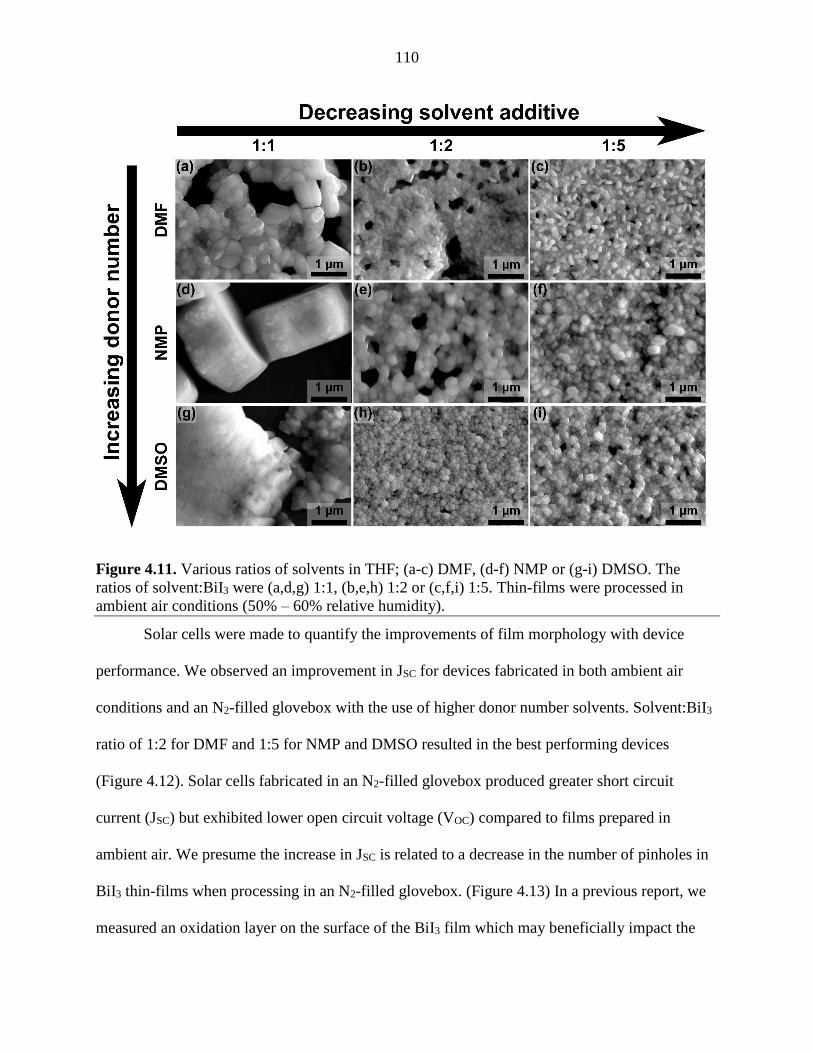
110
Figure 4.11. Various ratios of solvents in THF; (a-c) DMF, (d-f) NMP or (g-i) DMSO. The
ratios of solvent:BiI3 were (a,d,g) 1:1, (b,e,h) 1:2 or (c,f,i) 1:5. Thin-films were processed in
ambient air conditions (50% – 60% relative humidity).
Solar cells were made to quantify the improvements of film morphology with device
performance. We observed an improvement in JSC for devices fabricated in both ambient air
conditions and an N2-filled glovebox with the use of higher donor number solvents. Solvent:BiI3
ratio of 1:2 for DMF and 1:5 for NMP and DMSO resulted in the best performing devices
(Figure 4.12). Solar cells fabricated in an N2-filled glovebox produced greater short circuit
current (JSC) but exhibited lower open circuit voltage (VOC) compared to films prepared in
ambient air. We presume the increase in JSC is related to a decrease in the number of pinholes in
BiI3 thin-films when processing in an N2-filled glovebox. (Figure 4.13) In a previous report, we
measured an oxidation layer on the surface of the BiI3 film which may beneficially impact the

111
VOC.31 The VOC of BiI3 is predicted to be 1.1 eV,35 but may be limited by intrinsic defects that
may exist within the film.61,62
Figure 4.12. J-V characterization of BiI3 thin films solar cells fabricated in ambient air (RH 50-
60%) and N2-filled glovebox. DMF (1:2 DMF:BiI3), NMP (1:5 NMP:BiI3), and DMSO (1:5
DMSO:BiI3) solvent additives were used for device characterization.

112
Figure 4.13. SEM of films processed from BiI3 in THF with 1:2 solvent additives:BiI3. In
ambient air (RH 50 -60%) (a) No SA, (b) DMF, (c) DMSO, (d) NMP. In N2-filled glovebox (e)
No SA, (f) DMF, (g) DMSO, (h) NMP.

113
4.5. Summary and Conclusions
By utilizing strongly coordinating solvents, we demonstrated the ability to manipulate the
film morphology of solution-processed BiI3 thin film morphology. Controlling the relative molar
ratios of solvent additive:BiI3 dissolved in THF to solvents with a higher DN than THF (such as
DMF, NMP, and DMSO) enabled us to tune the surface coverage, the aggregate size, and the
preferred orientation of the BiI3 thin-film. Based on these results, we believe DN can be used as a
guide to control the crystallization and optimize the film morphology of solution processed Bi
halides and Bi halide perovskite inspired thin films.
4.6. Acknowledgments
The authors thank Dr. Matt Besser from the Ames Laboratory for his assistance in
acquiring XRD measurements. RDN and BJR acknowledge support from the National Science
Foundation Graduate Research Fellowship Program under DGE 1744592. MGP acknowledges
support from the Herbert L. Stiles Faculty Fellowship. The authors would also like to
acknowledge support from the AFOSR Young Investigator Program, under Grant # FA9550-17-
1-0170.
4.7. References
(1) Best Research Cell Efficiencies https://www.nrel.gov/pv/assets/pdfs/pv-efficiency-
chart.20190103.pdf (accessed Jan 18, 2019).
(2) Seok, S. I.; Grätzel, M.; Park, N.-G. Methodologies toward Highly Efficient Perovskite Solar
Cells. Small 14 (20), 1704177. https://doi.org/10.1002/smll.201704177.
(3) Green, M. A.; Ho-Baillie, A.; Snaith, H. J. The Emergence of Perovskite Solar Cells. Nat
Photon 2014, 8 (7), 506–514.
(4) Stranks, S. D.; Snaith, H. J. Metal-Halide Perovskites for Photovoltaic and Light-Emitting
Devices. Nat Nano 2015, 10 (5), 391–402.
(5) Han, Y.; Meyer, S.; Dkhissi, Y.; Weber, K.; Pringle, J. M.; Bach, U.; Spiccia, L.; Cheng, Y.-
B. Degradation Observations of Encapsulated Planar CH3NH3PbI3 Perovskite Solar Cells at
114
High Temperatures and Humidity. J. Mater. Chem. A 2015, 3 (15), 8139–8147.
https://doi.org/10.1039/C5TA00358J.
(6) Yi, C.; Luo, J.; Meloni, S.; Boziki, A.; Ashari-Astani, N.; Grätzel, C.; Zakeeruddin, S. M.;
Röthlisberger, U.; Grätzel, M. Entropic Stabilization of Mixed A-Cation ABX3 Metal Halide
Perovskites for High Performance Perovskite Solar Cells. Energy Environ. Sci. 2016, 9 (2),
656–662. https://doi.org/10.1039/C5EE03255E.
(7) Cho, H.; Kim, Y.-H.; Wolf, C.; Lee, H.-D.; Lee, T.-W. Improving the Stability of Metal
Halide Perovskite Materials and Light-Emitting Diodes. Adv. Mater. 0 (0), 1704587.
https://doi.org/10.1002/adma.201704587.
(8) Bert, C.; Jeroen, D.; Nicolas, G.; Aslihan, B.; Jan, D.; Lien, D.; Anitha, E.; Jo, V.; Jean, M.;
Edoardo, M.; et al. Intrinsic Thermal Instability of Methylammonium Lead Trihalide
Perovskite. Adv. Energy Mater. 5 (15), 1500477. https://doi.org/10.1002/aenm.201500477.
(9) Berhe, T. A.; Su, W.-N.; Chen, C.-H.; Pan, C.-J.; Cheng, J.-H.; Chen, H.-M.; Tsai, M.-C.;
Chen, L.-Y.; Dubale, A. A.; Hwang, B.-J. Organometal Halide Perovskite Solar Cells:
Degradation and Stability. Energy Env. Sci 2016, 9 (2), 323–356.
https://doi.org/10.1039/C5EE02733K.
(10) Correa-Baena, J.-P.; Saliba, M.; Buonassisi, T.; Grätzel, M.; Abate, A.; Tress, W.;
Hagfeldt, A. Promises and Challenges of Perovskite Solar Cells. Science 2017, 358 (6364),
739–744. https://doi.org/10.1126/science.aam6323.
(11) Babayigit, A.; Ethirajan, A.; Muller, M.; Conings, B. Toxicity of Organometal Halide
Perovskite Solar Cells. Nat. Mater. 2016, 15, 247.
(12) Eperon, G. E.; Stranks, S. D.; Menelaou, C.; Johnston, M. B.; Herz, L. M.; Snaith, H. J.
Formamidinium Lead Trihalide: A Broadly Tunable Perovskite for Efficient Planar
Heterojunction Solar Cells. Energy Env. Sci 2014, 7 (3), 982–988.
https://doi.org/10.1039/C3EE43822H.
(13) Protesescu, L.; Yakunin, S.; Bodnarchuk, M. I.; Krieg, F.; Caputo, R.; Hendon, C. H.;
Yang, R. X.; Walsh, A.; Kovalenko, M. V. Nanocrystals of Cesium Lead Halide Perovskites
(CsPbX3, X = Cl, Br, and I): Novel Optoelectronic Materials Showing Bright Emission with
Wide Color Gamut. Nano Lett. 2015, 15 (6), 3692–3696. https://doi.org/10.1021/nl5048779.
(14) De Wolf, S.; Holovsky, J.; Moon, S.-J.; Löper, P.; Niesen, B.; Ledinsky, M.; Haug, F.-J.;
Yum, J.-H.; Ballif, C. Organometallic Halide Perovskites: Sharp Optical Absorption Edge
and Its Relation to Photovoltaic Performance. J. Phys. Chem. Lett. 2014, 5 (6), 1035–1039.
https://doi.org/10.1021/jz500279b.
(15) Stranks, S. D.; Eperon, G. E.; Grancini, G.; Menelaou, C.; Alcocer, M. J.; Leijtens, T.;
Herz, L. M.; Petrozza, A.; Snaith, H. J. Electron-Hole Diffusion Lengths Exceeding 1

115
Micrometer in an Organometal Trihalide Perovskite Absorber. Science 2013, 342 (6156),
341–344.
(16) Brandt, R. E.; Stevanović, V.; Ginley, D. S.; Buonassisi, T. Identifying Defect-Tolerant
Semiconductors with High Minority-Carrier Lifetimes: Beyond Hybrid Lead Halide
Perovskites. Mrs Commun. 2015, 5 (2), 265–275.
(17) Hoye, R. L. Z.; Brandt, R. E.; Osherov, A.; Stevanović, V.; Stranks, S. D.; Wilson, M. W.
B.; Kim, H.; Akey, A. J.; Perkins, J. D.; Kurchin, R. C.; et al. Methylammonium Bismuth
Iodide as a Lead-Free, Stable Hybrid Organic–Inorganic Solar Absorber. Chem. – Eur. J.
2016, 22 (8), 2605–2610. https://doi.org/10.1002/chem.201505055.
(18) Nelson, R. D.; Santra, K.; Wang, Y.; Hadi, A.; Petrich, J. W.; Panthani, M. G. Synthesis
and Optical Properties of Ordered-Vacancy Perovskite Cesium Bismuth Halide
Nanocrystals. Chem Commun 2018, 54 (29), 3640–3643.
https://doi.org/10.1039/C7CC07223F.
(19) Yang, B.; Chen, J.; Hong, F.; Mao, X.; Zheng, K.; Yang, S.; Li, Y.; Pullerits, T.; Deng,
W.; Han, K. Lead-Free, Air-Stable All-Inorganic Cesium Bismuth Halide Perovskite
Nanocrystals. Angew. Chem. Int. Ed. 56 (41), 12471–12475.
https://doi.org/10.1002/anie.201704739.
(20) Singh, T.; Kulkarni, A.; Ikegami, M.; Miyasaka, T. Effect of Electron Transporting Layer
on Bismuth-Based Lead-Free Perovskite (CH3NH3)3 Bi2I9 for Photovoltaic Applications.
ACS Appl. Mater. Interfaces 2016, 8 (23), 14542–14547.
https://doi.org/10.1021/acsami.6b02843.
(21) Lindqvist, O.; Johansson, G.; Sandberg, F.; Norin, T. Crystal Structure of Caesium
Bismuth Iodide, Cs3Bi2I9. Acta Chem Scand 1968, 22, 2943–2952.
(22) Ran, C.; Wu, Z.; Xi, J.; Yuan, F.; Dong, H.; Lei, T.; He, X.; Hou, X. Construction of
Compact Methylammonium Bismuth Iodide Film Promoting Lead-Free Inverted Planar
Heterojunction Organohalide Solar Cells with Open-Circuit Voltage over 0.8 V. J. Phys.
Chem. Lett. 2017, 8 (2), 394–400. https://doi.org/10.1021/acs.jpclett.6b02578.
(23) Park, B.-W.; Philippe, B.; Zhang, X.; Rensmo, H.; Boschloo, G.; Johansson, E. M. J.
Bismuth Based Hybrid Perovskites A3Bi2I9 (A: Methylammonium or Cesium) for Solar
Cell Application. Adv. Mater. 2015, 27 (43), 6806–6813.
https://doi.org/10.1002/adma.201501978.
(24) Ghosh, B.; Chakraborty, S.; Wei, H.; Guet, C.; Li, S.; Mhaisalkar, S.; Mathews, N. Poor
Photovoltaic Performance of Cs3Bi2I9: An Insight through First-Principles Calculations. J.
Phys. Chem. C 2017, 121 (32), 17062–17067. https://doi.org/10.1021/acs.jpcc.7b03501.

116
(25) Pal, J.; Bhunia, A.; Chakraborty, S.; Manna, S.; Das, S.; Dewan, A.; Datta, S.; Nag, A.
Synthesis and Optical Properties of Colloidal M3Bi2I9 (M = Cs, Rb) Perovskite
Nanocrystals. J. Phys. Chem. C 2018. https://doi.org/10.1021/acs.jpcc.8b03542.
(26) Meloche, C.; Clark, P. CESIUM BISMUTH IODIDE. J. Am. Chem. Soc. 1930, 52 (3),
907–910.
(27) Lintereur, A. T.; Qiu, W.; Nino, J. C.; Baciak, J. Characterization of Bismuth Tri-Iodide
Single Crystals for Wide Band-Gap Semiconductor Radiation Detectors. Symp. Radiat.
Meas. Appl. SORMA XII 2010 2011, 652 (1), 166–169.
https://doi.org/10.1016/j.nima.2010.12.013.
(28) Boopathi, K. M.; Raman, S.; Mohanraman, R.; Chou, F.-C.; Chen, Y.-Y.; Lee, C.-H.;
Chang, F.-C.; Chu, C.-W. Solution-Processable Bismuth Iodide Nanosheets as Hole
Transport Layers for Organic Solar Cells. Sol. Energy Mater. Sol. Cells 2014, 121, 35–41.
https://doi.org/10.1016/j.solmat.2013.10.031.
(29) Brandt, R. E.; Kurchin, R. C.; Hoye, R. L. Z.; Poindexter, J. R.; Wilson, M. W. B.;
Sulekar, S.; Lenahan, F.; Yen, P. X. T.; Stevanović, V.; Nino, J. C.; et al. Investigation of
Bismuth Triiodide (BiI3) for Photovoltaic Applications. J. Phys. Chem. Lett. 2015, 6 (21),
4297–4302. https://doi.org/10.1021/acs.jpclett.5b02022.
(30) Lehner, A. J.; Wang, H.; Fabini, D. H.; Liman, C. D.; Hébert, C.-A.; Perry, E. E.; Wang,
M.; Bazan, G. C.; Chabinyc, M. L.; Seshadri, R. Electronic Structure and Photovoltaic
Application of BiI3. Appl. Phys. Lett. 2015, 107 (13), 131109.
https://doi.org/10.1063/1.4932129.
(31) Hamdeh, U. H.; Nelson, R. D.; Ryan, B. J.; Bhattacharjee, U.; Petrich, J. W.; Panthani,
M. G. Solution-Processed BiI3 Thin Films for Photovoltaic Applications: Improved Carrier
Collection via Solvent Annealing. Chem. Mater. 2016, 28 (18), 6567–6574.
https://doi.org/10.1021/acs.chemmater.6b02347.
(32) Fabian, D. M.; Ardo, S. Hybrid Organic-Inorganic Solar Cells Based on Bismuth Iodide
and 1,6-Hexanediammonium Dication. J Mater Chem A 2016, 4 (18), 6837–6841.
https://doi.org/10.1039/C6TA00517A.
(33) Coutinho, N. F.; Merlo, R. B.; Borrero, N. F.; Marques, F. C. Thermal Evaporated
Bismuth Triiodide (BiI3) Thin Films for Photovoltaic Applications. MRS Adv. 2018, 1–4.
(34) Kulkarni, A.; Singh, T.; Jena, A. K.; Pinpithak, P.; Ikegami, M.; Miyasaka, T. Vapor
Annealing Controlled Crystal Growth and Photovoltaic Performance of Bismuth Triiodide
Embedded in Mesostructured Configurations. ACS Appl. Mater. Interfaces 2018, 10 (11),
9547–9554. https://doi.org/10.1021/acsami.8b00430.
(35) Williamson, B. W.; Eickemeyer, F. T.; Hillhouse, H. W. Solution-Processed BiI3 Films
with 1.1 EV Quasi-Fermi Level Splitting: The Role of Water, Temperature, and Solvent

117
during Processing. ACS Omega 2018, 3 (10), 12713–12721.
https://doi.org/10.1021/acsomega.8b00813.
(36) Hamill, J. C.; Schwartz, J.; Loo, Y.-L. Influence of Solvent Coordination on Hybrid
Organic–Inorganic Perovskite Formation. ACS Energy Lett. 2017, 92–97.
https://doi.org/10.1021/acsenergylett.7b01057.
(37) Shin, S. S.; Correa Baena, J. P.; Kurchin, R. C.; Polizzotti, A.; Yoo, J. J.; Wieghold, S.;
Bawendi, M. G.; Buonassisi, T. Solvent-Engineering Method to Deposit Compact Bismuth-
Based Thin Films: Mechanism and Application to Photovoltaics. Chem. Mater. 2018, 30 (2),
336–343. https://doi.org/10.1021/acs.chemmater.7b03227.
(38) Burgués-Ceballos, I.; Savva, A.; Georgiou, E.; Kapnisis, K.; Papagiorgis, P.; Mousikou,
A.; Itskos, G.; Othonos, A.; Choulis, S. A. The Influence of Additives in the Stoichiometry
of Hybrid Lead Halide Perovskites. AIP Adv. 2017, 7 (11), 115304.
https://doi.org/10.1063/1.5010261.
(39) Manser, J. S.; Saidaminov, M. I.; Christians, J. A.; Bakr, O. M.; Kamat, P. V. Making
and Breaking of Lead Halide Perovskites. Acc. Chem. Res. 2016, 49 (2), 330–338.
https://doi.org/10.1021/acs.accounts.5b00455.
(40) Wu, L.-M.; Wu, X.-T.; Chen, L. Structural Overview and Structure–Property
Relationships of Iodoplumbate and Iodobismuthate. Funct. Hybrid Nanomater. 2009, 253
(23), 2787–2804. https://doi.org/10.1016/j.ccr.2009.08.003.
(41) Yang, M.; Li, Z.; Reese, M. O.; Reid, O. G.; Kim, D. H.; Siol, S.; Klein, T. R.; Yan, Y.;
Berry, J. J.; van Hest, M. F. A. M.; et al. Perovskite Ink with Wide Processing Window for
Scalable High-Efficiency Solar Cells. 2017, 2, 17038.
(42) Öz, S.; Hebig, J.-C.; Jung, E.; Singh, T.; Lepcha, A.; Olthof, S.; Jan, F.; Gao, Y.;
German, R.; Loosdrecht, P. H. M. van; et al. Zero-Dimensional (CH3NH3)3Bi2I9 Perovskite
for Optoelectronic Applications. Sol. Energy Mater. Sol. Cells 2016, 158, 195–201.
https://doi.org/10.1016/j.solmat.2016.01.035.
(43) Wang, P.; Zhang, X.; Zhou, Y.; Jiang, Q.; Ye, Q.; Chu, Z.; Li, X.; Yang, X.; Yin, Z.;
You, J. Solvent-Controlled Growth of Inorganic Perovskite Films in Dry Environment for
Efficient and Stable Solar Cells. Nat. Commun. 2018, 9 (1), 2225.
https://doi.org/10.1038/s41467-018-04636-4.
(44) Bush, K. A.; Rolston, N.; Gold-Parker, A.; Manzoor, S.; Hausele, J.; Yu, Z. J.; Raiford, J.
A.; Cheacharoen, R.; Holman, Z. C.; Toney, M. F.; et al. Controlling Thin-Film Stress and
Wrinkling during Perovskite Film Formation. ACS Energy Lett. 2018, 3 (6), 1225–1232.
https://doi.org/10.1021/acsenergylett.8b00544.

118
(45) Salim, T.; Sun, S.; Abe, Y.; Krishna, A.; Grimsdale, A. C.; Lam, Y. M. Perovskite-Based
Solar Cells: Impact of Morphology and Device Architecture on Device Performance. J
Mater Chem A 2015, 3 (17), 8943–8969. https://doi.org/10.1039/C4TA05226A.
(46) Eperon, G. E.; Burlakov, V. M.; Docampo, P.; Goriely, A.; Snaith, H. J. Morphological
Control for High Performance, Solution-Processed Planar Heterojunction Perovskite Solar
Cells. Adv. Funct. Mater. 2014, 24 (1), 151–157. https://doi.org/10.1002/adfm.201302090.
(47) Liang, P.-W.; Liao, C.-Y.; Chueh, C.-C.; Zuo, F.; Williams, S. T.; Xin, X.-K.; Lin, J.;
Jen, A. K.-Y. Additive Enhanced Crystallization of Solution-Processed Perovskite for Highly
Efficient Planar-Heterojunction Solar Cells. Adv. Mater. 2014, 26 (22), 3748–3754.
https://doi.org/10.1002/adma.201400231.
(48) Jeon, N. J.; Noh, J. H.; Kim, Y. C.; Yang, W. S.; Ryu, S.; Seok, S. I. Solvent Engineering
for High-Performance Inorganic–Organic Hybrid Perovskite Solar Cells. Nat. Mater. 2014,
13, 897.
(49) Xu, P.; Mujumdar, A.; Yu, B. Drying-Induced Cracks in Thin Film Fabricated from
Colloidal Dispersions. Dry. Technol. 2009, 27, 636–652.
https://doi.org/10.1080/07373930902820804.
(50) Routh, A. F.; Russel, W. B. Deformation Mechanisms during Latex Film Formation:
Experimental Evidence. Ind. Eng. Chem. Res. 2001, 40 (20), 4302–4308.
https://doi.org/10.1021/ie001070h.
(51) Routh, A. F.; Russel, W. B. A Process Model for Latex Film Formation: Limiting
Regimes for Individual Driving Forces. Langmuir 1999, 15 (22), 7762–7773.
https://doi.org/10.1021/la9903090.
(52) Ye, T.; Suo, Z.; Evans, A. G. Thin Film Cracking and the Roles of Substrate and
Interface. Int. J. Solids Struct. 1992, 29 (21), 2639–2648. https://doi.org/10.1016/0020-
7683(92)90227-K.
(53) Kim, Y. S.; Lee, Y.; Kim, J. K.; Seo, E.-O.; Lee, E.-W.; Lee, W.; Han, S.-H.; Lee, S.-H.
Effect of Solvents on the Performance and Morphology of Polymer Photovoltaic Devices.
Curr. Appl. Phys. 2010, 10 (4), 985–989. https://doi.org/10.1016/j.cap.2009.10.013.
(54) Chang, J.-F.; Sun, B.; Breiby, D. W.; Nielsen, M. M.; Sölling, T. I.; Giles, M.;
McCulloch, I.; Sirringhaus, H. Enhanced Mobility of Poly(3-Hexylthiophene) Transistors by
Spin-Coating from High-Boiling-Point Solvents. Chem. Mater. 2004, 16 (23), 4772–4776.
https://doi.org/10.1021/cm049617w.
(55) Gutmann, V.; Wychera, E. Coordination Reactions in Non Aqueous Solutions - The Role
of the Donor Strength. Inorg. Nucl. Chem. Lett. 1966, 2 (9), 257–260.
https://doi.org/10.1016/0020-1650(66)80056-9.

119
(56) Gutmann, V. Empirical Parameters for Donor and Acceptor Properties of Solvents.
Electrochimica Acta 1976, 21 (9), 661–670. https://doi.org/10.1016/0013-4686(76)85034-7.
(57) Reichardt, C.; Welton, T. Solvents and Solvent Effects in Organic Chemistry; John Wiley
& Sons, 2011.
(58) Haynes, W. M. CRC Handbook of Chemistry and Physics; CRC press, 2014.
(59) Nørby, P.; Jørgensen, M. R. V.; Johnsen, S.; Brummerstedt Iversen, B. Bismuth Iodide
Hybrid Organic-Inorganic Crystal Structures and Utilization in Formation of Textured BiI3
Film. Eur. J. Inorg. Chem. 2016, 2016 (9), 1389–1394.
https://doi.org/10.1002/ejic.201501418.
(60) Foley, B. J.; Girard, J.; Sorenson, B. A.; Chen, A. Z.; Scott Niezgoda, J.; Alpert, M. R.;
Harper, A. F.; Smilgies, D.-M.; Clancy, P.; Saidi, W. A.; et al. Controlling Nucleation,
Growth, and Orientation of Metal Halide Perovskite Thin Films with Rationally Selected
Additives. J Mater Chem A 2017, 5 (1), 113–123. https://doi.org/10.1039/C6TA07671H.
(61) Cho, S. B.; Gazquez, J.; Huang, X.; Myung, Y.; Banerjee, P.; Mishra, R. Intrinsic Point
Defects and Intergrowths in Layered Bismuth Triiodide. Phys. Rev. Mater. 2018, 2 (6),
064602. https://doi.org/10.1103/PhysRevMaterials.2.064602.
(62) Tiwari, D.; Alibhai, D.; Fermin, D. J. Above 600 MV Open-Circuit Voltage BiI3 Solar
Cells. ACS Energy Lett. 2018, 3 (8), 1882–1886.
https://doi.org/10.1021/acsenergylett.8b01182.

120
CHAPTER 5. SOLUTION-PROCESSED BISMUTH HALIDE PEROVSKITE THIN
FILMS: INFLUENCE OF DEPOSITION CONDITIONS AND A-SITE ALLOYING ON
MORPHOLOGY AND OPTICAL PROPERTIES
Modified from a manuscript submitted to the American Chemical Society Journal of Physical
Chemistry Letters
Reproduced with permission from American Chemical Society Journal of Physical Chemistry
Letters, submitted for publication. Unpublished work copyright 2019 American Chemical
Society
Umar H. Hamdeh,† Bradley J. Ryan,† Rainie D. Nelson,† Michael Zembrzuski,† Jonathan
Slobidsky,† Kevin J. Prince,† Iver Cleveland,† and Matthew G. Panthani†,*
†Department of Chemical and Biological, Iowa State University, Ames, Iowa 50011, United
States of America
5.1. Abstract
Bismuth halide perovskites have been proposed as a potential nontoxic alternative to
lead-based halide perovskites; however, they have not realized suitable performance. The poor
performance has been attributed to substandard film morphologies and too wide of a band gap
for many applications. Herein, we used a two-step deposition procedure to convert BiI3 thin films
into A3Bi2I9 (A = FA+, MA+, Cs+, and/or Rb+), which resulted in a substantial improvement in
film morphology, a larger band gap, and more compositional tunability compared to the
conventional single-step deposition. Additionally, AxRb3-xBi2I9 thin films were fabricated in
effort to reduce the undesirably wide band gap by inducing chemical pressures through cation
size mismatch to produce compressive strain within the 2D Rb3Bi2I9 octahedra. However, we
find that Rb3Bi2I9 with A-site substitution always forms the 0D structure and no changes to the
optical absorption were observed, implying that the band gap is insensitive to A-site alloying.

121
5.2. Introduction
Lead-based halide perovskites have tremendous potential as optoelectronic materials
owing to their tunable band gaps,1 high absorption coefficients,2 large diffusion lengths,3 solution
processability,4,5 and defect tolerance.6 Their power conversion efficiencies (PCEs) have
reached 23.7%,7 making them a potential competitor to traditional photovoltaic (PV)
technologies; however, their commercialization may be hindered by the toxicity of lead.8–10
Thus, replacing Pb2+ with isoelectronic Bi3+ provides potential routes for chemically-stable and
non-toxic perovskites.
Bismuth halide perovskites adopt an ordered vacancy structure with an A3Bi2I9 (A =
formamidinium (FA+), methylammonium (MA+), Cs+, Rb+, etc.) chemical formula, with most
prior work having focused on MA3Bi2I9.11–30 The most common approach for fabricating A3Bi2I9
thin films involves spin coating solutions that contain stoichiometric quantities of soluble
precursors; this “single-step” deposition has led to PV devices with ~1% efficiency.13–21,31
Alternatively, “two-step” deposition procedures have also been reported; here, BiI3 films are first
deposited and then converted to the A3Bi2I9 perovskite by additional processing in the solution-
phase,24–26 vapor-phase,24,27,32 or a combination of the two.28–30 Prior two-step deposition studies
have focused on improving film morphology and surface coverage, and have resulted in PCEs as
high as 3.17%.30 Although solution-based two-step deposition techniques have been developed
for MA3Bi2I9 and FA3Bi2I9,24–26 these techniques have not yet been developed for Rb3Bi2I9 or
Cs3Bi2I9, likely due to the tendency of BiI3 to dissolve in commonly used solvents that are used
to dissolve alkali metal salts.33
The family of bismuth halide perovskites display compositional flexibility like their lead-
based analogs.34 However, their band gaps are too wide for many applications;13,14,35–38 some
attribute this to the low-dimensional structures (i.e., “0D” and “2D” structures) that the bismuth

122
halide semiconductors tend to adopt.39 Tunable electronic properties can be achieved through
structural distortion of 2D and 3D lead halide perovskites; octahedral compression from
mechanical or chemical pressures (larger A-site cations) results in narrower band gaps.40–43 In the
case of the 0D A3Bi2I9 structure, the band gap is insensitive to compositional changes of the A-
site cation; large organic A-site cations cause the Bi2I9 bioctahedra to elongate due to long-range
hydrogen bonding.36 Additionally, lower-dimensional materials have strong confinement effects
which can increase the effective mass of carriers and impede carrier extraction.44,45 Strategies
focusing on manipulating the connectivity and distortion of the Bi-I polyhedra could serve as a
viable route to reduce the band gap of bismuth halide perovskites and improve device
performance.36
We hypothesized that forming the 2D A3Bi2I9 phase could allow us to reduce the band
gap by inducing chemical pressure through cation size mismatch. Cation size mismatch has been
shown to mimic the impact of mechanical pressure,40,46 and has been used to engineer the band
gap of 3D bismuth halide double perovskites.47,48 Furthermore, unlike other A3Bi2I9 compounds,
Rb3Bi2I9 was recently determined to exist within a 2D crystal structure that consists of stacked
sheets of corrugated layers of corner-connected BiI6 octahedra.35 By alloying the 2D Rb3Bi2I9
with larger A-site cations, we set out to enable band gap tuning in AxRb3-xBi2I9 thin films by
inducing chemical pressure with cation size mismatch.
Here, we report our findings regarding the two primary limitations that hinder the
performance of A3Bi2I9 perovskite optoelectronic devices: poor film morphologies and an
undesirably wide band gap. We developed a solution-based processing technique to convert
compact BiI3 thin films to A3Bi2I9 to overcome challenges with film quality that others have
reported. To address the limitation of the undesirably wide band gap of 0D A3Bi2I9 we attempted

123
to reduce the band gap of 2D Rb3Bi2I9 thin films by inducing chemical pressure through cation
size mismatch. Our results highlight the improvements using the two-step deposition method
compared to the conventional single-step technique and the limitations of compressive strain,
due to cation size mismatch, on the 0D structure signifying a necessity to increase the
dimensionality of bismuth halide perovskites to tune the band gap.
5.3. Experimental Methods
5.3.1. Chemicals
Acetone (Sigma Aldrich, ≥99.5%), Isopropanol (Sigma Aldrich, ≥99.5%), Titanium
diisopropoxide bis(acetylacetonate) (Sigma Aldrich, 75 wt% in isopropanol), Ethanol (Sigma
Aldrich, anhydrous, ≤ 0.003 % water), TiO2 paste, BiI3 (Beantown Chemical, 99.999% trace
metals basis), Tetrahydrofuran (THF; Acros Organics, 99.9% extra pure, anhydrous, stabilied
with BHT), Dimethylsulfoxide (DMSO; Sigma Aldrich, anhydrous, ≥ 99.9%),
Dimethylformamide (DMF; Sigma Aldrich, anhydrous, 99.8%), Formamindum iodide (FAI;
Dyesol), Methylammonimum iodide (MAI; Dyesol), Cesium iodide (CsI; Sigma Aldrich,
99.999% trace metals basis), Rubidium iodide (RbI; Sigma Aldrich 99.9% trace metals basis), 2-
propanol (IPA; Sigma Aldrich, anhydrous, 99.5%), hydroiodic acid (HI; Sigma Aldrich, 57 wt.
% in H2O, distilled, stabilized, 99.95%).
5.3.2. Solution preparation
BiI3 and AxRb3-xBi2I9 (A = FA+, MA+, Cs+) solutions were prepared in an N2-filled
glovebox unless stated otherwise. For the single-step deposition, AxRb3-xBi2I9 solutions, were
prepared using an adaptation of a previous report.13 Briefly, 0.5 M solutions of AxRb3-xBi2I9
solutions were made by dissolving stoichiometric quantities of BiI3, AI, and RbI powders in a
solution containing a 7:3 volumetric ratio of DMF:DMSO; these solutions were then sonicated

124
until completely dissolved (~30 min) and filtered through a 0.2 µm PTFE filter immediately
before use.
For the two-step deposition, BiI3 was dissolved at a concentration of 100 mg/mL in
anhydrous THF, followed by an addition of DMSO at a 2:1 molar ratio of BiI3:DMSO as
described elsewhere.49 0.125 mM solutions of AI were prepared by separately dissolving FAI,
MAI, or RbI in a solution containing a 19:1 volumetric ratio of IPA:H2O under ambient
conditions. For CsI, a 3:2 volumetric ratio of IPA:H2O was used. Aqueous HI (57 wt% in H2O)
was added to the AI solution in molar ratio 1:1 of HI:AI. For the two-step alloying, solutions
containing both RbI and FAI or MAI were prepared by combing the pure solutions in molar
ratios of 2:1, 1:1, or 1:2 of AI:RbI. For solutions containing CsI and RbI, a 3:2 volumetric ratio
of IPA:H2O was used for both CsI and RbI salt solutions.
5.3.3. Thin-Film Fabrication
FTO substrate preparation. FTO substrates (Hartford Glass, Tec 7, 25 mm x 25 mm x
2.2 mm, 6-8 ohm/sq) were cleaned throughly prior to use. Substrates were sonicated in detergent
water (DeconTM ContrexTM AP Labware Detergent) for 20 minutes and throughly rinsed with
Milli-Q water. Then, the substrates were subsequently sonicated in Milli-Q water, Acetone, and
Isopropanol for 20 minutes for each solvent. Afterwards, the substrates were thorughly rinsed
with Milli-Q water and blown dry with ultra-high pure N2, and UV treated with O2 plasma for 20
minutes. TiO2 deposition was performed immediately after UV treatment.
Sol-gel preparation and deposition of TiO2 layer. 20 mL of a 0.4 M TiO2 sol-gel was
made by combining 3.4 mL of titanium diisopropoxide bis(acetylacetonate) and 16.6 mL of
ethanol in a N2-filled glovebox. All subsequent processing was done in ambient air conditions
(RH 50 – 60%). A thin layer of compact TiO2 (c-TiO2) was deposited through a 0.2 µm PTFE
filter onto the FTO substrate until the entire substrate is covered and then spun at 4500 RPM for

125
30 seconds in a spin coater under ambient conditions. The substrate was then placed on a 3/8”
thick aluminum block on top of a hotplate, with the temperature of the aluminum block set at
~450 °C (temperature measured with a thermocouple that was placed into the center of the
aluminum block) and annealed for at least 30 minutes. The substrates were removed from the
aluminum block and allowed to cool naturally.
20 mL of a mesoporous TiO2 (m-TiO2) sol-gel was prepared by mixing 4.5 g of TiO2 paste in 20
mL of ethanol. The paste was sonicated for 30–60 minutes. 200 µL of the sol-gel was deposted
onto the c-TiO2 layer and spun at 3000 RPM for 30 seconds in a spin coater under ambient
conditions. The substrate was then placed on a 3/8” thick aluminum block on top of a hotplate,
with the temperature of the aluminum block set at ~450 °C and annealed for at least 30 minutes.
The substrates were removed from the aluminum block and allowed to cool naturally. TiO2
coated FTO substrates were stored in a N2-filled glovebox until further use.
AxRb3-xBi2I9 thin film deposition. All films were prepared under ambient conditions and
deposited onto m-TiO2 coated FTO substrates. The single-step deposition of AxRb3-xBi2I9 was
conducted by adapting a previous report.13 Briefly, 200 µL of the AxRb3-xBi2I9 solution was
deposited onto the substrate and spin coated at 1500 RPM for 30 seconds followed by annealing
at 110 °C for 30 minutes. Afterwards, the AxRb3-xBi2I9 thin films were removed from the hot
plate and cooled to room temperature.
For the two-step deposition of AxRb3-xBi2I9, 200 µL of the BiI3 solution was deposited
onto the substrate and spin coated at 2000 RPM for 60 seconds followed by annealing at 150 °C
for 20 minutes. Afterwards, the BiI3 thin films were removed from the hot plate and cooled to
room temperature. Next, 200 µL of the AI solution was deposited onto the BiI3 film and spin

126
coated at 2000 RPM for 60 seconds followed by annealing at 150 °C for 20 minutes; CsxRb3-
xBi2I9 (for x>0) were annealed for 8 hours instead of 20 minutes.
5.3.4. Equipment Characterization List
Transmittance and reflectance data were collected on a PerkinElmer Lambda 750
spectrophotometer equipped with a Labsphere 100 mm integrating sphere; this data was used to
calculate absorbance. A Kubelka-Munk (KM) transformation was performed on the diffuse
reflectance data, from which band gaps were extracted using Tauc analysis of an indirect band
gap. Powder X-Ray diffraction (XRD) of films was measured using a Bruker DaVinci D8
Advance diffractometer with a Cu Kα radiation source. Scanning electron microscope (SEM)
images were taken with a FEI Quanta 250 FE-SEM with an accelerating voltage of 15-20 kV.
5.4. Results and Discussion
We first focused on addressing the deposition procedure for A3Bi2I9 thin films to improve
the film morphology. SEM images of the conventional single-step deposited A3Bi2I9 films reveal
the films exhibit irregular surface coverage with large crystallites protruding from the surface,
similar to previous reports (Figure 5.1).13,36 We note that cracking of FA3Bi2I9 thin films
occurred during imaging, suggesting either incomplete solvent removal during annealing, or
degradation during imaging. Tauc analysis suggest the band gaps for all A3Bi2I9 films are ~2.1
eV, agreeing with previous reports (Figure 5.1).13,14,35–37
Chemical Water Solubility
Cesium Iodide (CsI) 848.43 mg/mL (25 °C)
Rubidium Iodide (RbI) 1652.52 mg/mL (25 °C)
Bismuth Triiodide (BiI3) 7.80 x 10⁻³ mg/mL (20 °C)
Table 5.1. Solubility of A3Bi2I9 (A = Cs+, or Rb+) precursors in water.33

127
Figure 5.1. Characterization of films produced using the single-step deposition. SEM images of
(a) Rb3Bi2I9, (b) Cs3Bi2I9, (c) MA3Bi2I9, and (d) FA3Bi2I9 films. (e) Tauc plots of diffuse-
reflectance absorption.
Informed by previous studies of MA3Bi2I9,24 we initially selected isopropanol (IPA) to
dissolve AI (A = FA+, MA+, Cs+, or Rb+) precursors; however, we find that CsI and RbI are not
soluble at sufficiently high concentrations to completely convert the films into A3Bi2I3. Thus, we
used a volumetric mixture of IPA and H2O to dissolve RbI and CsI (IPA:H2O; 19:1 and 3:2
respectively). HI(aq) was added to all solutions containing H2O to inhibit oxidation of BiI3 into
Bi2O3. The thickness of a BiI3 film was previously estimated at 200 nm,50 and the concentration
of AI was set to ~10x molar excess with respect to BiI3. HI(aq) was added in equimolar amounts
to the AI salts and this solution is referred to as “acidic IPA/H2O” hereafter. The BiI3 films were
completely transformed into A3Bi2I9 (Figure 5.2), as shown by the disappearance of the
absorption onset at ~1.8 eV which is characteristic to BiI3. We further characterized this

128
conversion using X-ray diffraction (XRD) (Figure 5.3 – 5.5), showing that all films were phase-
pure, except for Rb3Bi2I9, and no detectible BiI3 remained after the two-step deposition.
Figure 5.2. (a) SEM image of a BiI3 thin film. (b) Image of a BiI3 thin film prior to two-step
deposition. (c) Image of MA3Bi2I9 thin film post two-step deposition. Film color representative
of A3Bi2I9 films. (d) UV-Vis characterization of BiI3 and A3Bi2I9 thin films. No absorbance from
BiI3 is measured in A3Bi2I9 films after two-step deposition.
.
Figure 5.3. XRD characterization of initial BiI3 thin film and two-step A3Bi2I9 (A = FA+, MA+,
Cs+, and Rb+) thin films deposited on TiO2 coated FTO substrates. * denotes the diffraction
peaks of the m-TiO2 coated FTO substrate. Dashed lines are to guide the eye.

129
Figure 5 4. XRD characterization of one- and two-step (a) FA3Bi2I9 and (b) MA3Bi2I9 thin films
deposited on TiO2 coated FTO substrates. * denotes the diffraction peaks of the TiO2 coated FTO
substrate. MA3Bi2I9 reference pattern from Hoye et al.24 FA3Bi2I9 reference pattern simulated
with the lattice parameters reported by Huang et al.36

130
Figure 5.5. XRD characterization of one- and two-step (a) Cs3Bi2I9 and (b) Rb3Bi2I9 thin films
deposited on TiO2 coated FTO substrates. * denotes the diffraction peaks of the TiO2 coated FTO
substrate. Peaks not related to the Rb3Bi2I9 phase are labeled with an ‘o’. Cs3Bi2I9 reference
pattern from Arakcheeva et al.51 and Rb3Bi2I9 reference pattern from Lehner et al.35
We used UV-Vis characterization to probe the effect of acidified IPA/H2O on the
oxidation of BiI3 thin films. We spin coated pure acidified IPA/H2O onto a BiI3 film, mimicking
the procedure for the two-step deposition, and measured no changes in the absorbance of the BiI3

131
thin film (Figure 5.6). We find that the BiI3 thin films appear to be unaffected over the course of
~3 minutes when exposed to acidified IPA/H2O.
Figure 5.6. Effect of the acidified IPA/H2O solution on the absorbance spectra of a BiI3 thin
film. The acidified IPA/H2O solution was spin coated onto the BiI3 film to mimic the conditions
of the two-step deposition procedure.
Since organic AI salts (A = FA+, and MA+) are soluble in IPA, water is not necessary for
the conversion of BiI3 to A3Bi2I9 (A = FA+, and MA+). Therefore, we used organic AI salts to
probe any differences that may occur by using the acidified IPA/H2O solution. We converted
BiI3 thin films to A3Bi2I9 by using both IPA and the acidified IPA/H2O solution to dissolve
organic AI salts. The thin films were characterized with UV-Vis and XRD (Figure 5.7). The
diffusion of AI into BiI3 is more rapid when using the acidified IPA/H2O solution compared to
using IPA. Multiple deposition steps are necessary for the full conversion of BiI3 to A3Bi2I9
when using IPA, while only one deposition step was necessary for the acidified IPA/H2O
solution. FA3Bi2I9 thin films produced from using the acidified IPA/H2O solution resulted in a
lower absorbance compared to using IPA; however, both thin films exhibited phase pure XRD
patterns. The lower absorbance measurement suggests that the acidified IPA/H2O solution may
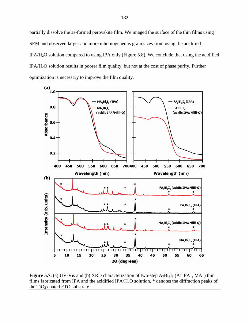
132
partially dissolve the as-formed perovskite film. We imaged the surface of the thin films using
SEM and observed larger and more inhomogeneous grain sizes from using the acidified
IPA/H2O solution compared to using IPA only (Figure 5.8). We conclude that using the acidified
IPA/H2O solution results in poorer film quality, but not at the cost of phase purity. Further
optimization is necessary to improve the film quality.
Figure 5.7. (a) UV-Vis and (b) XRD characterization of two-step A3Bi2I9 (A= FA+, MA+) thin
films fabricated from IPA and the acidified IPA/H2O solution. * denotes the diffraction peaks of
the TiO2 coated FTO substrate.

133
Figure 5.8. SEM characterization of two-step A3Bi2I9 (A= FA+, MA+) thin films fabricated from
IPA and the acidified IPA/H2O solution.
The rate of conversion to A3Bi2I9 was markedly different, and did not correlate to the
cationic radii (FA+, MA+, Cs+, and Rb+ are 2.53, 2.16, 1.88, and 1.72 Å, respectively).52,53 We
found that the conversion of BiI3 films to FA3Bi2I9, MA3Bi2I9, and Rb3Bi2I9 was immediate;
however, conversion to Cs3Bi2I9 required 8 hours of thermal annealing at 150 °C. Prolonged
exposure of BiI3 films to the RbI solution completely dissolved the films. The two-step deposited
Rb3Bi2I9 films were more yellow in appearance than the single-step deposition, which were
orange, similar to what was observed with the other A3Bi2I9 films. We hypothesize two-step
deposited Rb3Bi2I9 films undergo partial oxidation during fabrication and will require further
experimentation to improve the purity.

134
Figure 5.9. Characterization of films produced using the two-step deposition. SEM images of (a)
Rb3Bi2I9, (b) Cs3Bi2I9, (c) MA3Bi2I9, and (d) FA3Bi2I9 thin films. (e) Tauc plots of diffuse-
reflectance absorption.
Figure 5.10. SEM images of two-step A3Bi2I9, (A = FA+, MA+, Cs+) thin films with varying AI
salt concentrations. Concentration of AI salt solutions were set to 0.125, 0.625, and 1.25 mM or
10x, 50x, or 100x molar excess of a 200 nm BiI3 thin film.
135
We compared the optical and morphological properties of A3Bi2I9 films produced using
the single- and two-step deposition procedures. SEM images show that films produced using
two-step deposition are smoother, have improved surface coverage, and are more homogenous in
grain size compared to films produced using single-step deposition (Figure 5.9a-d). The surface
roughness in the two-step deposited films is attributed to the expansion of the BiI3 film due to A-
site cation insertion (ca. 214%, 196%, 193%, and 247% volume increase per Bi atom relative to
BiI3 for FA+, MA+, Cs+, and Rb+, respectively). Varying the AI concentration was found to have
a dramatic impact on film morphology (Figure 5.10) and should be considered when optimizing
the two-step deposition of A3Bi2I9 thin films (see Supporting Information). Kubelka-Munk
transformations of the diffuse reflectance (KM) demonstrates that the band gaps for two-step
deposited A3Bi2I9 films are greater compared to single-step deposited films of the same
composition (Figures 5.1e and .5.9e). Previous reports indicate that smaller grain sizes result in
wider band gaps ranging between 1.96 and 2.26 eV in MA3Bi2I9, and an apparent blue shift in
optical absorption when crushing single crystals into fine powder.14 The increase in band gap
may be attributed to the smaller grain sizes with two-step A3Bi2I9 films, although further
investigation is needed to determine the source of band gap deviation.
The A3Bi2I9 films deposited using the single- and two-step methods have starkly different
XRD patterns (Figure 5.11). Films prepared using the single-step deposition show preferential
orientation along the c-axis, consistent with previous reports corresponding to the 0D crystal
structure.36 Lehner et al. reported that Rb3Bi2I9 forms a 2D crystal structure,35 contrasting the
findings of Huang et al., who found that Rb3Bi2I9 thin films were better described by the 0D
crystal structure.36 We find that dimensionality of single-step deposited Rb3Bi2I9 films cannot be
distinguished, as both 0D and 2D patterns have similar d-spacing for the (002), (004), and (006)

136
diffraction planes. XRD demonstrates that A3Bi2I9 films fabricated using two-step deposition
have randomly orientated grains, agreeing with previous reports.24,32 In contrast to the single-step
deposition, Rb3Bi2I9 films deposited with the two-step technique can only be described by the 2D
crystal structure.
Figure 5.11. XRD characterization of A3Bi2I9 (A = FA+, MA+, Cs+, Rb+) films produced from
the (a) single-step and (b) two-step deposition. * denotes diffraction peaks due to the
background. ╪ denotes a diffraction peak corresponding to a phase impurity found in Rb3Bi2I9.
For two-step, the amorphous feature below 20° 2θ is from the glass substrate.
After addressing the limitations in film morphology of A3Bi2I9 thin films, we turned our
attention to addressing the undesirably wide band gap of A3Bi2I9 compounds (~2.1 eV).
Compositional tuning is commonly used to vary the band gap;40–43 however, the band gap of the
0D structure of A3Bi2I9 compounds is thought to be insensitive to compositional tuning of the A-
site cation.36 Therefore, we propose increasing the dimensionality of bismuth halide perovskite
semiconductors is necessary to enable variations in the band gap with compositional tuning of
the A-site cation.
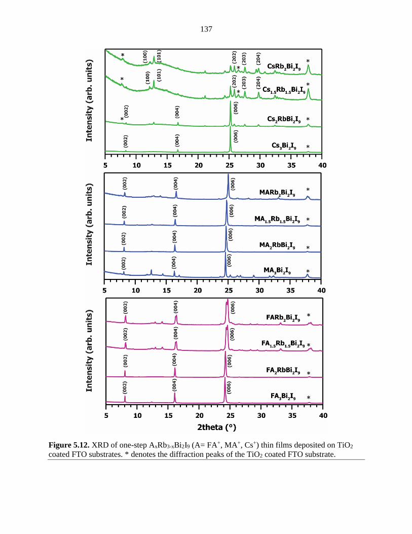
137
Figure 5.12. XRD of one-step AxRb3-xBi2I9 (A= FA+, MA+, Cs+) thin films deposited on TiO2
coated FTO substrates. * denotes the diffraction peaks of the TiO2 coated FTO substrate.

138
Figure 5.13. XRD of two-step AxRb3-xBi2I9 (A= FA+, MA+, Cs+) thin films deposited on TiO2
coated FTO substrates. * denotes the diffraction peaks of the TiO2 coated FTO substrate.

139
We hypothesized that A-site mismatch with large cations in the 2D Rb3Bi2I9 structure
could induce compressive strain on the Bi-I polyhedra, causing the band gap to narrow.
Chemical pressures induced from cation size mismatch are known to result in similar effects to
mechanical pressure,46 which can significantly impact the optical properties of lead halide
perovskites.40 Furthermore, cation size mismatch has been effectively used to narrow the band
gap in 3D bismuth halide double perovskites,47,48 and is a promising route to tune the band gap of
bismuth halide perovskites. Finally, lower-dimensional materials have strong confinement
effects which can decrease electronic charge transport.44,45 Therefore, increasing dimensionality
is expected to improve the performance of bismuth halide perovskite-based PV devices.54–57
We sought to alloy 2D Rb3Bi2I9 with other A-site cations in effort to form 2D AxRb3-
xBi2I9 (A = FA+, MA+, Cs+) and tune the optical band gap (Figure 5.12 and 5.13). For FAxRb3-
xBi2I9 and MAxRb3-xBi2I9 films deposited using the single-step method, we observed an
expansion of the crystal lattice corresponding to the {001} diffraction planes with increasing x;
this is likely due to strain from cation size mismatch. At x = 1.5, we observed phase segregation
in FAxRb3-xBi2I9, represented by the splitting of the diffraction peaks in the {001} family. This
peak splitting is likely due to the large difference in ionic radius between FA+ and Rb+ resulting
in the formation of FA-rich and Rb-rich phases. We do not observe phase segregation in the
MAxRb3-xBi2I9 system. In the case of CsxRb3-xBi2I9, the addition of Rb+ caused a transition from
intense peaks belonging to the {001} planes to intense peaks belonging to the (101), (202),
(203), and (204) planes within the 0D hexagonal crystal structure of Cs3Bi2I9.51 Overall, the 2D
phase was not preserved in AxRb3-xBi2I9 films produced using the single-step deposition method.
For the two-step deposition of FAxRb3-xBi2I9 and MAxRb3-xBi2I9, we also observed an
isotropic expansion of the crystal lattice with increasing x, as suggested by a shift to lower 2θ in

140
all diffraction peaks. Unlike the single-step deposited films, we did not observe any peak
splitting in the FAxRb3-xBi2I9 films. For CsxRb3-xBi2I9, there was a decrease in the
crystallographic orientation along the (202) plane with increasing x within the 0D phase for
Cs3Bi2I9. Regardless of processing method, AxRb3-xBi2I9 films formed the 0D structure for all x
> 0. This suggests that there is a preference for forming the 0D crystal structure within this
compositional range.
We characterized the relationship between composition and band gap by plotting the
measured band gap and the d-spacing for the (001) plane (d001-spacing) for AxRb3-xBi2I9 films
(Figure 5.14; Tauc analysis is shown in Figure 5.15). Although the c-axis changes by nearly 5%
with compositional tuning, there was no difference in the optical band gap. We conclude that the
band gap of AxRb3-xBi2I9 is insensitive to cation size mismatch and lattice constant, while
preferentially forming the 0D structure, similar to what was reported elsewhere.36 Finally, to
correlate composition and d001-spacing, we used Vegard’s law to empirically determine the
composition of the FAxRb3-xBi2I9 and MAxRb3-xBi2I9 films (Figure 5.16). We found that the final
composition of the alloys predicted through Vegard’s law deviated from the initial solution and
did not follow a linear relation. This deviation from the linear trend is observed for both the one-
and two-step deposition procedures indicating that the change in composition with alloying is
independent of the processing conditions.

141
Figure 5.14. (a) XRD of AxRb3-xBi2I9 films deposited using the single-step deposition procedure.
(b) Band gaps for the one- and two-step deposition of AxRb3-xBi2I9 films are plotted as a function
of d001-spacing.
Figure 5.15. Vegard’s law analysis for one- and two-step AxRb3-xBi2I9 (A= FA+, MA+) thin
films. AxRb3-xBi2I9 (A = FA+, MA+) thin films do not follow Vegard’s law and deviate from a
linear shift in d001-spacing with increasing composition of FA+ and MA+. FAxRb3-xBi2I9 and
MAxRb3-xBi2I9 are represented by violet and blue respectively. Rb3Bi2I9 is represented with red.

142
Figure 5.16. Normalized Tauc plots of the KM data for the (a) one- and (b) two-step AxRb3-
xBi2I9 (A = FA+, MA+, Cs+) thin films assuming indirect bandgaps.

143
5.5. Summary and Conclusions
In conclusion, we report our attempts to address two limitations that have hindered the
usefulness of bismuth-based perovskites: poor film morphology and undesirably wide band gaps.
To address the morphology issue, we successfully developed a two-step solution-based
deposition method to synthesize A3Bi2I9 (A= FA+, MA+, Cs+, and Rb+) perovskite thin films. The
two-step deposition procedure resulted in more uniform grain size and surface coverage
compared to the single-step deposition procedure. Unexpectedly, the band gap of two-step
deposited A3Bi2I9 increased relative to the single-step. We speculate that this could be due to the
presence of small or poorly-formed crystallites after A-site cation insertion;14 however, further
investigation is required to determine the origin of this increase in band gap. To address the wide
band gap of 0D A3Bi2I9 compounds, we attempted to alloy the 2D Rb3Bi2I9 structure and reduce
the band gap with large chemical pressures through cation size mismatch. We prepared AxRb3-
xBi2I9 (A= FA+, MA+, Cs+) thin films using both the single- and two-step deposition procedures.
We found that alloying 2D Rb3Bi2I9 films with FA+, MA+, and Cs+ did not result in films with
the 2D phase, but rather the lower-dimensional 0D phase. We demonstrate that cation size
mismatch had no discernable impact on the band gap, as initially considered by Huang et al.36
These results suggest that the band gaps of bismuth halide perovskites are insensitive to
structural modification, strain, and composition. Further advancements of bismuth halide
perovskites should focus on alternative strategies such as increasing the structural dimensionality
to access narrower band gaps and improve electronic properties for optoelectronic applications.
5.6. Acknowledgments
The authors would like to acknowledge funding from the Air Force Office of Scientific
Research Young Investigator Program FA9550-17-1-0170. MGP would like to acknowledge
support from the Herbert L. Stiles Faculty Fellowship. UHH acknowledges support from the

144
DOE under DE-AC52-07NA27344. RDN and BJR acknowledge support from the National
Science Foundation Graduate Research Fellowship Program under DGE 1744592. The authors
thank Dr. Matt Besser from the Ames Laboratory for his assistance in acquiring XRD
measurements.
5.7. References
1. Eperon, G. E. et al. Formamidinium lead trihalide: a broadly tunable perovskite for efficient
planar heterojunction solar cells. Energy Env. Sci 7, 982–988 (2014).
2. De Wolf, S. et al. Organometallic Halide Perovskites: Sharp Optical Absorption Edge and Its
Relation to Photovoltaic Performance. J. Phys. Chem. Lett. 5, 1035–1039 (2014).
3. Stranks, S. D. et al. Electron-hole diffusion lengths exceeding 1 micrometer in an
organometal trihalide perovskite absorber. Science 342, 341–344 (2013).
4. You, J. et al. Low-Temperature Solution-Processed Perovskite Solar Cells with High
Efficiency and Flexibility. ACS Nano 8, 1674–1680 (2014).
5. Dou, B. et al. Roll-to-Roll Printing of Perovskite Solar Cells. ACS Energy Lett. 3, 2558–
2565 (2018).
6. Brandt, R. E., Stevanović, V., Ginley, D. S. & Buonassisi, T. Identifying defect-tolerant
semiconductors with high minority-carrier lifetimes: beyond hybrid lead halide perovskites.
Mrs Commun. 5, 265–275 (2015).
7. Best Research Cell Efficiencies. Best Research Cell Efficiencies (2018). Available at:
https://www.nrel.gov/pv/assets/pdfs/pv-efficiency-chart.20190103.pdf. (Accessed: 18th
January 2019)
8. J. Juarez-Perez, E. et al. Photodecomposition and thermal decomposition in
methylammonium halide lead perovskites and inferred design principles to increase
photovoltaic device stability. J. Mater. Chem. A 6, 9604–9612 (2018).
9. Bert, C. et al. Intrinsic Thermal Instability of Methylammonium Lead Trihalide Perovskite.
Adv. Energy Mater. 5, 1500477
10. Müller, C. et al. Water Infiltration in Methylammonium Lead Iodide Perovskite: Fast and
Inconspicuous. Chem. Mater. 27, 7835–7841 (2015).
11. Szklarz, P. et al. Structure, phase transitions and molecular dynamics of [C(NH 2 ) 3 ] 3 [M
2 I 9 ], M = Sb, Bi. J. Phys. Condens. Matter 20, 255221 (2008).

145
12. Eckhardt, K. et al. Crystallographic insights into (CH3NH3)3(Bi2I9): a new lead-free hybrid
organic-inorganic material as a potential absorber for photovoltaics. Chem Commun 52,
3058–3060 (2016).
13. Park, B.-W. et al. Bismuth Based Hybrid Perovskites A3Bi2I9 (A: Methylammonium or
Cesium) for Solar Cell Application. Adv. Mater. 27, 6806–6813 (2015).
14. Abulikemu, M. et al. Optoelectronic and photovoltaic properties of the air-stable
organohalide semiconductor (CH3NH3)3Bi2I9. J Mater Chem A 4, 12504–12515 (2016).
15. Lyu, M. et al. Organic–inorganic bismuth (III)-based material: A lead-free, air-stable and
solution-processable light-absorber beyond organolead perovskites. Nano Res. 9, 692–702
(2016).
16. Öz, S. et al. Zero-dimensional (CH3NH3)3Bi2I9 perovskite for optoelectronic applications.
Sol. Energy Mater. Sol. Cells 158, 195–201 (2016).
17. Singh, T., Kulkarni, A., Ikegami, M. & Miyasaka, T. Effect of Electron Transporting Layer
on Bismuth-Based Lead-Free Perovskite (CH3NH3)3 Bi2I9 for Photovoltaic Applications.
ACS Appl. Mater. Interfaces 8, 14542–14547 (2016).
18. Zhang, X. et al. Active-layer evolution and efficiency improvement of (CH3NH3
3Bi2I9-based solar cell on TiO2-deposited ITO substrate. Nano Res. 9, 2921–2930 (2016).
19. Kulkarni, A., Singh, T., Ikegami, M. & Miyasaka, T. Photovoltaic enhancement of bismuth
halide hybrid perovskite by N-methyl pyrrolidone-assisted morphology conversion. RSC Adv
7, 9456–9460 (2017).
20. Okano, T. & Suzuki, Y. Gas-assisted coating of Bi-based (CH3NH3)3Bi2I9 active layer in
perovskite solar cells. Mater. Lett. 191, 77–79 (2017).
21. Shin, S. S. et al. Solvent-Engineering Method to Deposit Compact Bismuth-Based Thin
Films: Mechanism and Application to Photovoltaics. Chem. Mater. 30, 336–343 (2018).
22. Lan, C. et al. Effect of lead-free (CH3NH3)3Bi2I9 perovskite addition on spectrum
absorption and enhanced photovoltaic performance of bismuth triiodide solar cells. J. Alloys
Compd. 701, 834–840 (2017).
23. Mali, S. S., Kim, H., Kim, D.-H. & Hong, C. K. Anti-Solvent Assisted Crystallization
Processed Methylammonium Bismuth Iodide Cuboids towards Highly Stable Lead-Free
Perovskite Solar Cells. ChemistrySelect 2, 1578–1585 (2017).
24. Hoye, R. L. Z. et al. Methylammonium Bismuth Iodide as a Lead-Free, Stable Hybrid
Organic–Inorganic Solar Absorber. Chem. – Eur. J. 22, 2605–2610 (2016).

146
25. Wang, H. et al. Fabrication of methylammonium bismuth iodide through interdiffusion of
solution-processed BiI3/CH3NH3I stacking layers. RSC Adv 7, 43826–43830 (2017).
26. Wenderott, J. K., Raghav, A., Shtein, M., Green, P. F. & Satapathi, S. Local Optoelectronic
Characterization of Solvent-Annealed, Lead-Free, Bismuth-Based Perovskite Films.
Langmuir 34, 7647–7654 (2018).
27. Chen, X. et al. Atmospheric pressure chemical vapor deposition of methylammonium
bismuth iodide thin films. J Mater Chem A (2017). doi:10.1039/C7TA06578G
28. Ran, C. et al. Construction of Compact Methylammonium Bismuth Iodide Film Promoting
Lead-Free Inverted Planar Heterojunction Organohalide Solar Cells with Open-Circuit
Voltage over 0.8 V. J. Phys. Chem. Lett. 8, 394–400 (2017).
29. Zhang, Z. et al. High-Quality (CH3NH3)3Bi2I9 Film-Based Solar Cells: Pushing Efficiency
up to 1.64%. J. Phys. Chem. Lett. 8, 4300–4307 (2017).
30. Jain, S. M. et al. An effective approach of vapour assisted morphological tailoring for
reducing metal defect sites in lead-free, (CH3NH3)3Bi2I9 bismuth-based perovskite solar
cells for improved performance and long-term stability. Nano Energy 49, 614–624 (2018).
31. Johansson, M. B., Zhu, H. & Johansson, E. M. J. Extended Photo-Conversion Spectrum in
Low-Toxic Bismuth Halide Perovskite Solar Cells. J. Phys. Chem. Lett. 7, 3467–3471
(2016).
32. Khazaee, M. et al. A Versatile Thin-Film Deposition Method for Multidimensional
Semiconducting Bismuth Halides. Chem. Mater. 30, 3538–3544 (2018).
33. Haynes, W. M. CRC handbook of chemistry and physics. (CRC press, 2014).
34. Wu, L.-M., Wu, X.-T. & Chen, L. Structural overview and structure–property relationships
of iodoplumbate and iodobismuthate. Funct. Hybrid Nanomater. 253, 2787–2804 (2009).
35. Lehner, A. J. et al. Crystal and Electronic Structures of Complex Bismuth Iodides A3Bi2I9
(A = K, Rb, Cs) Related to Perovskite: Aiding the Rational Design of Photovoltaics. Chem.
Mater. 27, 7137–7148 (2015).
36. Huang, X., Huang, S., Biswas, P. & Mishra, R. Band Gap Insensitivity to Large Chemical
Pressures in Ternary Bismuth Iodides for Photovoltaic Applications. J. Phys. Chem. C 120,
28924–28932 (2016).
37. Ghosh, B. et al. Limitations of Cs3Bi2I9 as lead-free photovoltaic absorber materials. ACS
Appl. Mater. Interfaces (2018). doi:10.1021/acsami.7b14735
38. Shockley, W. & Queisser, H. J. Detailed Balance Limit of Efficiency of p‐n Junction Solar
Cells. J. Appl. Phys. 32, 510–519 (1961).

147
39. Li, M.-Q. et al. Structure Tunable Organic–Inorganic Bismuth Halides for an Enhanced
Two-Dimensional Lead-Free Light-Harvesting Material. Chem. Mater. 29, 5463–5467
(2017).
40. Jaffe, A., Lin, Y. & Karunadasa, H. I. Halide Perovskites under Pressure: Accessing New
Properties through Lattice Compression. ACS Energy Lett. 2, 1549–1555 (2017).
41. Amat, A. et al. Cation-Induced Band-Gap Tuning in Organohalide Perovskites: Interplay of
Spin–Orbit Coupling and Octahedra Tilting. Nano Lett. 14, 3608–3616 (2014).
42. Jaffe, A. et al. High-Pressure Single-Crystal Structures of 3D Lead-Halide Hybrid
Perovskites and Pressure Effects on their Electronic and Optical Properties. ACS Cent. Sci. 2,
201–209 (2016).
43. Prasanna, R. et al. Band Gap Tuning via Lattice Contraction and Octahedral Tilting in
Perovskite Materials for Photovoltaics. J. Am. Chem. Soc. 139, 11117–11124 (2017).
44. Saparov, B. et al. Thin-Film Preparation and Characterization of Cs3Sb2I9: A Lead-Free
Layered Perovskite Semiconductor. Chem. Mater. 27, 5622–5632 (2015).
45. Milot, R. L. et al. Charge-Carrier Dynamics in 2D Hybrid Metal–Halide Perovskites. Nano
Lett. 16, 7001–7007 (2016).
46. Morón, M. C., Palacio, F. & Clark, S. M. Pressure-induced structural phase transitions in the
AMnF4 series (A=Cs, Rb, K) studied by synchrotron x-ray powder diffraction: Correlation
between hydrostatic and chemical pressure. Phys Rev B 54, 7052–7061 (1996).
47. Slavney, A. H. et al. Defect-Induced Band-Edge Reconstruction of a Bismuth-Halide Double
Perovskite for Visible-Light Absorption. J. Am. Chem. Soc. 139, 5015–5018 (2017).
48. Slavney, A. H. et al. Small-Band-Gap Halide Double Perovskites. Angew. Chem. Int. Ed. 57,
12765–12770 (2018).
49. Hamdeh, U. H., Nelson, R. D., Bradley J. Ryan & Panthani, M. G. The Effects of Solvent
Coordination Strength on the Morphology of Solution-Processed BiI3 Thin Films. Submitt.
Publ. (2019).
50. Hamdeh, U. H. et al. Solution-Processed BiI3 Thin Films for Photovoltaic Applications:
Improved Carrier Collection via Solvent Annealing. Chem. Mater. 28, 6567–6574 (2016).
51. Arakcheeva, A., Bonin, M., Chapuis, G. & Zaitsev, A. The phases of Cs3Bi2I9 between RT
and 190 K. Z. Krist. 214, 279–283 (1999).
52. Shannon, R. D. Revised effective ionic radii and systematic studies of interatomic distances
in halides and chalcogenides. Acta Crystallogr. Sect. A 32, 751–767

148
53. Travis, W., Glover, E. N. K., Bronstein, H., Scanlon, D. O. & Palgrave, R. G. On the
application of the tolerance factor to inorganic and hybrid halide perovskites: a revised
system. Chem Sci 7, 4548–4556 (2016).
54. Slavney, A. H. et al. Chemical Approaches to Addressing the Instability and Toxicity of
Lead–Halide Perovskite Absorbers. Inorg. Chem. 56, 46–55 (2017).
55. Igbari, F. et al. Composition Stoichiometry of Cs2AgBiBr6 Films for Highly Efficient Lead-
Free Perovskite Solar Cells. Nano Lett. 19, 2066–2073 (2019).
56. Slavney, A. H., Hu, T., Lindenberg, A. M. & Karunadasa, H. I. A Bismuth-Halide Double
Perovskite with Long Carrier Recombination Lifetime for Photovoltaic Applications. J. Am.
Chem. Soc. 138, 2138–2141 (2016).
57. Volonakis, G. et al. Lead-Free Halide Double Perovskites via Heterovalent Substitution of
Noble Metals. J. Phys. Chem. Lett. 7, 1254–1259 (2016).

149
CHAPTER 6. CONCLUSIONS AND SUMMARY
Environmental concerns over the large-scale use of fossil fuels has prompted increased
financial investment and research effort in the development of solar power. Massive
infrastructural change is necessary to significantly decrease the use of fossil fuels in the coming
decades and minimize the environmental and social changes that are predicted to occur from
man-made global climate change. Thin film semiconductors provide advantages in
manufacturing compared to conventional silicon (Si) such as reduced material feedstock (>1 µm
films), high throughout and low temperature processing, and implementation in both solution and
vapor phase deposition processes. Using non-toxic Earth abundant materials would be
advantageous for wide spread solar panel installation into commercial and residential buildings
and in implementation into a variety of technologies. Earth abundant materials that do not
require intensive mining should also be considered to minimize the environmental impact in
acquiring mineral feedstock.
Hybrid organic-inorganic Pb halide perovskites are an emerging thin film semiconductor
that has gained an incredible amount of research attention in the past decade for its phenomenal
electronic properties. Hybrid organic-inorganic Pb halide perovskites thin film solar cells have
reached efficiencies as high as 23%, making them competitive with commercial Si solar cells.
They can be synthesized using solid, liquid, and vapor deposition processes, enabling a variety of
chemical processing for high throughput manufacturing. Unfortunately, hybrid organic-inorganic
Pb halide perovskites suffer from chemical instabilities and readily degrade in humid air, and in
temperatures exceeding 85 ºC. Research has focused on the chemistry of Pb halide perovskites to
improve the chemical stability and further increase the efficiency. Improving the chemical
stability will provide further incentive for wide-spread implementation of Pb halide perovskites

150
into commercial solar cells. Another drawback is the toxic nature of Pb. Although Pb is one of
the most abundant rare-earth elements, the biological impact on the human body makes it
unfavorable for commercial use. This has motivated a search for non-toxic alternatives to Pb
halide perovskites.
A list of properties was considered for potential candidates as non-toxic alternatives.
Common criteria for the active layer of thin film solar cells includes high absorption coefficient,
long carrier diffusion lengths, high carrier mobility, and an optimal bandgap for use in single
junction or tandem junction solar cells. Another criterion for the selection of a non-toxic
alternatives to Pb halide perovskites is finding materials with a similar electronic structure. Pb
halide perovskites are known to be ‘defect tolerant’ and can screen charged defects due to their
high dielectric constants. Furthermore, Pb halide perovskites possess shallow defect states that
exist near the band edge in contrast to more detrimental deep band gap states that will limit the
VOC of PV devices. By using computer simulations, researchers have targeted a list of non-toxic
materials that are predicted to possess these favorable properties. Bi-halide semiconductors have
emerged as an alternative class of materials and have embellished an uptick in research activity.
The relevance of this PhD dissertation is in the development of Bi halide semiconductors as a
non-toxic and chemical stable alternative class of materials to Pb halide perovskite
semiconductors.
Bi halide semiconductors have promising properties making them prospective
alternatives to Pb halide perovskite semiconductors. They possess similar electronic properties
and are predicted to defect tolerant. Bi halide semiconductors are advantageous to Pb halide
perovskites because of their chemical stability and nontoxic nature. Solar cells developed using
Bi halide semiconductors have not performed as efficiently as their Pb counterparts, however;

151
research on Bi halide semiconductors has only recently gained attention within the research
community. Much of the research has focused on improving the film morphology of Bi halide
semiconductors, and only recently have scientist begun to evaluate possible limiting factors. The
work presented in this dissertation was focused on improving the thin film morphology of Bi
halide semiconductors for future use in PV devices. This work provides a platform in which
further work into the electronic properties of Bi halide PV devices can be investigated.
The research attention was first prioritized to BiI3, since this metal halide is chemically
simple, and was predicted to maintain the excellent properties of MAPbI3. Molecular complexes
have been used widely over the past decade in “dimension reduction” approaches; however, in
most cases dimensional reduction requires the use of a relatively corrosive (reducing) solvent to
solubilize the inorganic material. In this case, BiI3 readily forms complexes with relatively
benign solvents in a similar manner to PbI2 — but unlike PbI2, the bandgap of BiI3 is suitable for
use as a PV absorber layer. We demonstrated that BiI3 forms molecular complexes with
coordinating solvents such as THF and DMF, enabling solution-based processing of BiI3 thin
films. We first set out to fabricate a proof-of-concept BiI3 thin film PV devices and then used this
baseline devices as a starting point for future investigation. We sought to improve the film
morphology of BiI3 thin films by solvent vapor annealing BiI3 thin films in coordinating solvents
to reform the thin film after deposition. By exposing the film to DMF solvent vapor we were able
to improve the grain size of the thin film and increase the JSC seven-fold. Based on
photoluminescence spectroscopy, we can infer that the improved performance is due to improved
carrier mobility since the excited-state lifetime does not increase after SVA. This processing led
to a 1.0 % efficient BiI3 devices, which at the time, was the best efficiency achieved with BiI3
used as the active layer. Processing in air provided multiple benefits to improving the PCE of

152
BiI3 thin film PVs: a BiOI layer forms at the surface that facilitates hole extraction. This work
demonstrated the potential of BiI3 as a non-toxic alternative to Pb-halide perovskites.
The formation of cracks in the BiI3 thin film became apparent when processing at higher
concentrations (> 200 mg/ml). Typically, BiI3 powder is dissolved in THF, but the weak
coordination of THF combined with the high vapor pressure causes the film to experience high
surface tension during spin processing and the films crack uncontrollably. Intrigued by the
impact that solvent vapor had on the film morphology of BiI3 thin films, we further investigated
the impact that solvent additives of highly coordinating solvents in solution could have on the
film morphology. Guided by the donor number of the solvents, we investigated the impact that
small volumetric additions of DMF, NMP, and DMSO to BiI3 dissolved in THF would have on
the film morphology. By controlling the amount of solvent additive, we were able to effectively
tune the film morphology from sparsely covered large grain thin films to crack-free compact
films. By optimizing the solvent additive volume, we were able to alleviate the cracking that
forms in BiI3 thin films and improve the morphology. The reduction in cracking led to an
improvement in device performance but was not as impactful as solvent vapor annealing. Most
importantly, we developed a technique that can be used a guideline for the processing other Bi-
halide semiconductors and showed that donor number is an important metric to consider when
designing the procedure for solution processed semiconductors.
The work done with BiI3 was extended to A3Bi2I9 (A = FA+, MA+, Cs+, or Rb+) thin films
which is another class of materials that can be used as alternative to Pb halide perovskites.
Challenges facing A3Bi2I9 semiconductors are the poor film morphology with conventional
processing techniques, and too wide of a bandgap for single junction PV application. The use of
a single-step deposition of A3Bi2I9 thin films results in poor film morphology which may hinder

153
the performance of bismuth halide perovskites in optoelectronic devices. A two-step deposition
procedure was developed to overcome the challenges with film morphology and improve device
performance. Single-step A3Bi2I9 thin films have a preferred crystallographic along the c-axis,
while two-step A3Bi2I9 films have more randomly orientated diffraction pattern that closely
resembles the powder pattern. The optical properties of A3Bi2I9 depend on the orientation of the
film and we measure a slight increase in the band gap with two-step processing. For the first
time, we extend a solution-based two-step deposition approach to all inorganic A3Bi2I9 thin
films.
After improving the film morphology, we set out to improve the optical properties of
A3Bi2I9. This class of material regularly forms a 0D structure that is insensitive to changes in
electronic properties due to varying the A-site cation. The insensitivity is due to the 0D crystal
structure which prevents variations to the bond lengths and angles of the Bi-I octahedra from
different A-site cation sizes. We hypothesized that increasing the dimensionality of A3Bi2I9 by
using the Rb3Bi2I9 2D polymorph may enable bandgap tuning through cation size mismatch of
the A-site cation. As such, we produced both the single- and two-step AxRb3-xBi2I9 (A = FA+,
MA+, or Cs+) thin films and measured the structural and optical properties. XRD characterization
of the crystal structure indicated that the 0D structure was preferentially forming in AxRb3-xBi2I9
thin films regardless of processing and that cation mismatch did not impact the optical bandgap.
We conclude that preferential formation of the 0D structure limits the effects of A-site alloying
and that alternative strategies should be considered to improve the dimensionality of Bi-halide
perovskite semiconductors.
In conclusion, this dissertation serves to inform the reader of strategies used to improve
the film morphology of Bi halide semiconductors for use in optoelectronic devices. Since

154
research on this material class is still in its infancy, the priority was to improve the film
morphology so that this is no longer the limiting factor to device performance. After the film
morphology is improved beyond a certain standard, the design of Bi halide semiconductors
should focus on improving the interface and band alignment between the p-type and n-type
semiconductors that sandwich the active layer. Once the device architecture is optimized, the
work should shift on improving the electronic properties of Bi halide semiconductors through
alloying or doping. Bi halide semiconductors are predicted to be “defect tolerant”, yet the VOC is
highly limited in PV devices. Research effort should focus on understanding what the limitations
to the VOC may be, and how to overcome these limitations. If the class of Bi halide
semiconductors are discovered not to be “defect tolerant” due to deep trap states within the
bandgap, for example, the criteria for “defect tolerance” should be reinvestigated and reapplied
to determine non-toxic materials as replacements for Pb-halide perovskites.