Thermoelectric and galvanomagnetic properties of bismuth chalcogenide nanostructured heteroepitaxial...
7
This content has been downloaded from IOPscience. Please scroll down to see the full text. Download details: IP Address: 194.85.224.35 This content was downloaded on 21/01/2015 at 06:56 Please note that terms and conditions apply. Thermoelectric and galvanomagnetic properties of bismuth chalcogenide nanostructured heteroepitaxial films View the table of contents for this issue, or go to the journal homepage for more 2015 Semicond. Sci. Technol. 30 015011 (http://iopscience.iop.org/0268-1242/30/1/015011) Home Search Collections Journals About Contact us My IOPscience
Transcript of Thermoelectric and galvanomagnetic properties of bismuth chalcogenide nanostructured heteroepitaxial...

This content has been downloaded from IOPscience. Please scroll down to see the full text.
Download details:
IP Address: 194.85.224.35
This content was downloaded on 21/01/2015 at 06:56
Please note that terms and conditions apply.
Thermoelectric and galvanomagnetic properties of bismuth chalcogenide nanostructured
heteroepitaxial films
View the table of contents for this issue, or go to the journal homepage for more
2015 Semicond. Sci. Technol. 30 015011
(http://iopscience.iop.org/0268-1242/30/1/015011)
Home Search Collections Journals About Contact us My IOPscience

Thermoelectric and galvanomagneticproperties of bismuth chalcogenidenanostructured heteroepitaxial films
L N Lukyanova1, Yu A Boikov1, V A Danilov1, O A Usov1, M P Volkov1,2 andV A Kutasov1
1 Ioffe Physical-Technical Institute, Russian Academy of Sciences, Polytekhnicheskaya 26, 194021 St.-Petersburg, Russia2 International Laboratory of High Magnetic Fields and Low Temperatures, 53-421, Wroclaw, Poland
E-mail: [email protected]
Received 12 July 2014, revised 15 October 2014Accepted for publication 30 October 2014Published 5 December 2014
AbstractHot wall technique was used to grow block single crystal films of Bi2Te3 and solid solutions ofBi0.5Sb1.5Te3 on mica (muscovite) substrates. X-ray diffraction studies demonstrated that thecrystalline c-axis in the films was normal to the substrate plane. Seebeck coefficient, electricalconductivity and magnetoresistivity tensor components were measured at various orientations ofmagnetic and electric fields in the temperature interval 77–300 K. Scattering mechanism ofcharge carriers in the films was studied using temperature dependences of the degeneracyparameter and the Seebeck coefficient in terms of a many-valley model of energy spectrum.Obtained results have shown that the effective scattering parameter is considerably differentfrom the value specific for an acoustic scattering of charge carriers in the weakly degeneratefilms due to an additional scattering of charge carriers on interface and interctystalliteboundaries. These features of charge carrier scattering are supposed to affect electronic transportin the films and enhance figure of merit.
Keywords: bismuth-telluride-based films, chalcogenides, transport properties, charge carrierscattering mechanism
(Some figures may appear in colour only in the online journal)
1. Introduction
It was shown [1–5] that nanostructured epitaxial films ofbismuth and antimony chalcogenides possess enhanced ther-moelectric figure of merit ZT as compared with that of thecorresponding bulk single crystals. Both mechanical stressesand intensive phonon scattering at the grain (block) bound-aries may contribute to enhanced efficiency of the bismuthand antimony chalcogenide films. Stresses may be induced bymismatch in lattice parameters of the thermoelectric film andused substrate or through the difference in correspondingthermal expansion coefficients. To provide selective impact ofthe grain boundaries on electron and phonon transport, theirstructure and charge state have to be optimized. c-axis in thegrains (blocks) should be strictly parallel to the substrate
normal. However, there has to be small (∼1 deg.) mis-orientation of the grains in the substrate plane.
The heteroepitaxial films under consideration are speci-fied by a high degree of anisotropy in most transport prop-erties. These thermoelectrics have a complex band structuredescribed in terms of the many-valley energy spectrummodel. The latter establishes the relations between their gal-vanomagnetic properties and the parameters determining theshape of constant-energy ellipsoids and charge carrier scat-tering mechanism [6–8].
Features of electron (hole) scattering mechanisms inheteroepitaxial films of Bi2Te3 and solid solution ofBi0.5Sb1.5Te3 are poorly documented in literature to date.
For development and optimization of a technology ofnanostructured epitaxial films based on high efficiency bulk
Semiconductor Science and Technology
Semicond. Sci. Technol. 30 (2015) 015011 (6pp) doi:10.1088/0268-1242/30/1/015011
0268-1242/15/015011+06$33.00 © 2015 IOP Publishing Ltd Printed in the UK1
thermoelectrics [9–12], the charge carrier scatteringmechanisms were investigated. Important information on theeffective scattering parameters and reduced Fermi levels infilms under consideration were revealed from the analysis ofgalvanomagnetic properties and the Seebeck coefficient ashas been carried out for bulk thermoelectrics.
Obtained experimental data and their analysis are con-sidered to be useful for formation of heteroepitaxial films withlarge power factor. That together with the reduction of latticethermal conductivity induced by selective phonon scatteringin low dimensional (thickness and/or grain size less than200 nm) films provides an enhancement of their thermo-electric figure of merit.
2. Samples for studies and structural investigations
Hot wall technique [13] was used to grow 50–500 nm thickepitaxial films of Bi2−xSbxTe3 (x= 0; 1.5) on (000l) mica(muscovite) substrates. An endemic feature of the hot walltechnique is abnormally high substrate temperature (TS)during a film growth. High TS promotes enhancement ofmobility of the particles (atoms, molecules and so on)adsorbed at a substrate surface. TS during thermoelectric layerformation was diminished just on 150 °C as compared withtemperature of the sublimating Bi2−xSbxTe3 powder. Toeliminate vapor phase condensation at the growth chamberwalls, temperature was about TS + 50 °C. An effective growthrate of the thermoelectric layer was in the range 1–3 Å s−1.
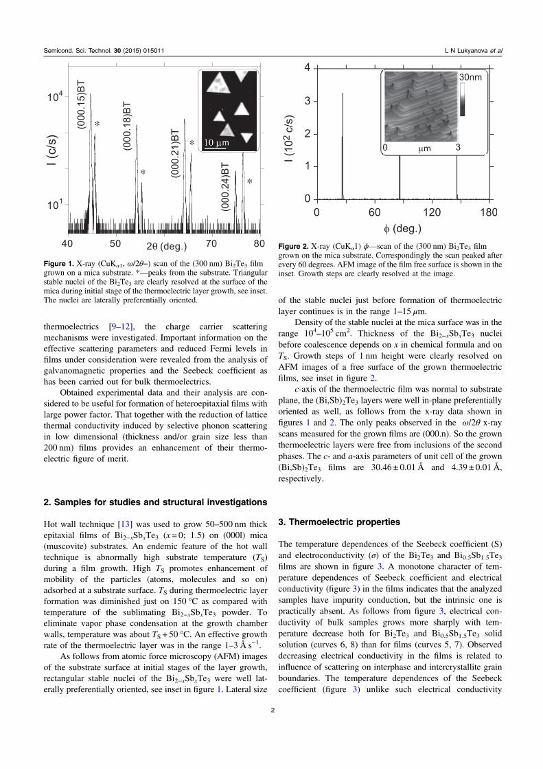
As follows from atomic force microscopy (AFM) imagesof the substrate surface at initial stages of the layer growth,rectangular stable nuclei of the Bi2−xSbxTe3 were well lat-erally preferentially oriented, see inset in figure 1. Lateral size
of the stable nuclei just before formation of thermoelectriclayer continues is in the range 1–15 μm.
Density of the stable nuclei at the mica surface was in therange 104–105 cm2. Thickness of the Bi2−xSbxTe3 nucleibefore coalescence depends on x in chemical formula and onTS. Growth steps of 1 nm height were clearly resolved onAFM images of a free surface of the grown thermoelectricfilms, see inset in figure 2.
c-axis of the thermoelectric film was normal to substrateplane, the (Bi,Sb)2Te3 layers were well in-plane preferentiallyoriented as well, as follows from the x-ray data shown infigures 1 and 2. The only peaks observed in the ω/2θ x-rayscans measured for the grown films are (000.n). So the grownthermoelectric layers were free from inclusions of the secondphases. The c- and a-axis parameters of unit cell of the grown(Bi,Sb)2Te3 films are 30.46 ± 0.01 Å and 4.39 ± 0.01 Å,respectively.
3. Thermoelectric properties
The temperature dependences of the Seebeck coefficient (S)and electroconductivity (σ) of the Bi2Te3 and Bi0.5Sb1.5Te3films are shown in figure 3. A monotone character of tem-perature dependences of Seebeck coefficient and electricalconductivity (figure 3) in the films indicates that the analyzedsamples have impurity conduction, but the intrinsic one ispractically absent. As follows from figure 3, electrical con-ductivity of bulk samples grows more sharply with tem-perature decrease both for Bi2Te3 and Bi0.5Sb1.5Te3 solidsolution (curves 6, 8) than for films (curves 5, 7). Observeddecreasing electrical conductivity in the films is related toinfluence of scattering on interphase and intercrystallite grainboundaries. The temperature dependences of the Seebeckcoefficient (figure 3) unlike such electrical conductivity
Figure 1. X-ray (CuKα1, ω/2θ−) scan of the (300 nm) Bi2Te3 filmgrown on a mica substrate. *—peaks from the substrate. Triangularstable nuclei of the Bi2Te3 are clearly resolved at the surface of themica during initial stage of the thermoelectric layer growth, see inset.The nuclei are laterally preferentially oriented.
Figure 2. X-ray (CuKα1) ϕ—scan of the (300 nm) Bi2Te3 filmgrown on the mica substrate. Correspondingly the scan peaked afterevery 60 degrees. AFM image of the film free surface is shown in theinset. Growth steps are clearly resolved at the image.
2
Semicond. Sci. Technol. 30 (2015) 015011 L N Lukyanova et al

dependences are located higher for films than for bulk Bi2Te3(curves 1, 2) and Bi0.5Sb1.5Te3 (curves 3, 4).
Enhancement of Seebeck coefficient and change of slopeof its temperature dependence indicate changes of chargecarrier scattering mechanisms and the parameters of theconstant-energy surface in grown films [7, 8] in comparisonwith those in bulk thermoelectric materials (figure 3, curves 1,2 and 3, 4, figure 4, curves 1, 3).
According to the data presented in [14], lattice con-tribution to thermal conductivity of c-axis orientedBi0.5Sb1.5Te3 films with a grain size about 200 nm is roughly30% diminished as compared with that for a correspondingbulk single crystal. It is worth mentioning that impact of thegrain boundaries on thermal conductivity of the Bi2Te3 filmsis substantially less than that for the solid solutions. That is aclear mark of considerable contribution of the long-wave-length phonons to the thermal conductivity of the solidsolutions based on bismuth and antimony chalcogenides.Thus, the large values of the power factor together with
decrease in thermal conductivity of the films lead to growth ofthe figure of merit Z [4, 5].
4. Galvanomagnetic properties and mechanisms ofcharge carriers scattering
The data about changes of charge carriers’ scatteringmechanisms in films and bulk thermoelectrics can be obtainedfrom comparative analysis of the galvanomagnetic and ther-moelectric properties. The galvanomagnetic properties werestudied for epitaxial Bi2−xSbxTe3 (x= 1.5) films in a widerange of magnetic field to 14 T in the temperature range77–300К.
The changes of magnetoresistivity tensor components inthe films are consistent with similar data obtained earlier forbulk materials [7]. The anisotropy of magnetoresistivity ten-sor components in the temperature range 77–300К (figures 5and 6, curves 1, 2) shows the change of anisotropy of con-stant-energy surface of the films. These tensor components
Figure 3. Temperature dependences of the Seebeck coefficient S(1–4), electroconductivity σ (5–8) for Bi2Te3 (1, 5) and Bi0.5Sb1.5Te3(3, 7) films, and for Bi2Te3 (2, 6) and Bi2−xSbxTe3 (4, 8) bulksamples.
Figure 4. Temperature dependences of the power factor S2σ forBi2Te3 (1) and Bi0.5Sb1.5Te3 (3) films, and for Bi2Te3 (2) and Bi2−xSbxTe3 (4) bulk samples.
Figure 5. Temperature dependence of the ratios of magnetoresistivitytensor components in Bi2Te3 (1–3) and Bi0.5Sb1.5Te3 (4–6) films.ρ1133/ρ1122—1, 4, ρ1133/ρ11111—2, 5, ρ1122/ρ11111—3, 6.
Figure 6. Temperature dependence of the Hall effect tensorcomponent ρ123 (1, 2) and the degeneracy parameter βd (3, 4) inBi2Te3 (1, 3) and Bi0.5Sb1.5Te3 (2, 4) films.
3
Semicond. Sci. Technol. 30 (2015) 015011 L N Lukyanova et al

measured at different orientations of magnetic and electricfields were analyzed with many-valley model of energyspectrum of charge carriers for isotropic scatteringmechanism.
The least square analysis of experimental data using themany-valley model of the energy spectrum of charge carriersand isotropic scattering mechanism permits determiningdegeneracy parameter (βd), and some parameters of the con-stant-energy ellipsoidal surfaces: such as effective masses andorientations of ellipsoids relative to the crystallographic axesthat characterized anisotropy of the constant-energy surfacesof films [7, 8]. The temperature dependence of the degeneracyparameter of the films is supposed to be explained by anadditional charge carrier scattering on interphase and inter-ctystallite boundaries of monocrystalline grains of the films(figure 6).
The degeneracy parameter βd in the framework of themany-valley model can be written as [6]:
β =I
I I, (1)d
12
0 2
where I0 is the electrical conductivity, I1 is the Hall con-ductivity, I2 is the magnetoconductivity. The generalexpression for In (n= 1, 2, 3) defined as:
⎜ ⎟⎛⎝
⎞⎠
⎛⎝⎜
⎞⎠⎟ ∫
π π ατ ε
εε=
∂∂
∞+I
e
m
e
m
m fd
3
2 1, (2)n
n
ij
n2
2 2
3/2
1/2 0
1 3/2 0
where an isotropic relaxation time τ τ= Er0 , and τ 0 is an
energy-independent factor.The parameter βd for isotropic relaxation time is given by
[12]:
β ηη
η η=
=+ +
+
+ +r
r F
r r F F( , )
(2 3/2) ( )
( 3/2)(3 3/2) ( ) ( ),(3)d
r
r r
22 1/22
1/2 3 1/2
here ηF ( )s are Fermi integrals of the type:
∫η =+η
∞
−Fx
edx( )
1, (4)s
s
x0
and η is the reduced Fermi level.The experimental values of the Seebeck coefficient α
depend on Fermi level and scattering parameter in the form:
⎡⎣⎢
⎤⎦⎥
ηη
η=++
−+
+S
k
e
r F
r F
( 2.5) ( )
( 1.5) ( ), (5)
r
r
1.5
0.5
The Fermi level (η) and effective scattering parameters(reff) that accounts for changing of the scattering mechanismin the films were obtained by solving two equations (3, 4) fordegeneracy parameter βd (r, η) and the Seebeck coefficient S(η, r) using Nelder–Mead least square method [12]. Residualfactor R(reff, η) [15] that characterized a discrepancy betweenexperimental and calculated values of accepted physicalmodel was evaluated to be less than 10−5, which permitsestimating η and r with accuracy less than 10−2 (figures 7and 8).
As the result of the experimental data analysis, it wasshown that for films and bulk bismuth telluride based
materials the value of effective scattering parameter reff ofcharge carriers differed markedly from widely used acousticscattering parameter r=−0.5 due to influence of charge car-riers of the second valence band specific for bismuth tellurideand its solid solutions.
The change of the parameter reff occurs not only due tosecond valence band of p-Bi2Te3 known for bulk materials[16] and strong electron–photon interaction, but also due to anadditional scattering of charge carriers on interphase andinterctystallite boundaries of monocrystalline blocks ofthe films.
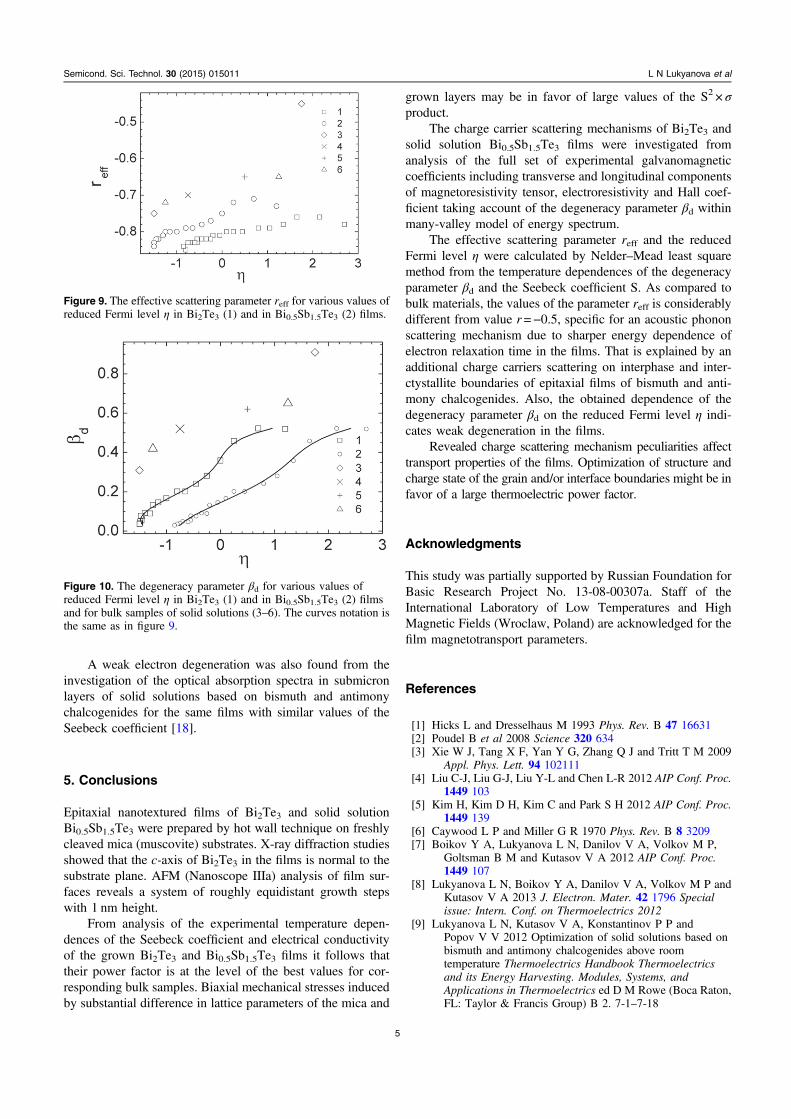
The obtained reff values in the films compared with bulkthermoelectrics shows more sharp energy dependence ofelectron relaxation time in the films for a model of isotropiccharge carrier scattering accepted for experimental data ana-lysis (figure 9, curves 1, 2 and points 3–6). As follows fromfigure 10, the dependence of the degeneracy parameter βd onthe reduced Fermi level η shows that the βd values in films aresmaller than in bulk materials. Therefore, the degeneracy offilms is smaller comparing with bulk thermoelectrics with thesame compositions (figure 10), since the βd = 1 at fulldegeneration. These specific dependences controlling scat-tering parameter of charge carriers lead to an increase in theincline of the Seebeck coefficient dependence on temperatureand enhancement of the thermoelectric power factor for films(figure 4, curves 1, 3).
Similar data for bulk samples of solid solutions: 3—Bi2−xSbxTe3−ySey [12] (x= 1.1, y = 0.09), 4—Bi2−xSbxTe3-ySey(x= 1.3, y= 0.07) [17], 5—Bi2−xSbxTe3 (x = 1.6) [17], 6—Bi2−xSbxTe3 (x= 1.1, y = 0.06) [12].
Figure 7. Residual factor R(reff, η) calculated for Bi2Te3 film at100 K for η = 2.7, r=−0.78.
Figure 8. Residual factor R(reff, η) calculated for Bi2Te3 film at300 K for η =−0.87, r = −0.84.
4
Semicond. Sci. Technol. 30 (2015) 015011 L N Lukyanova et al
A weak electron degeneration was also found from theinvestigation of the optical absorption spectra in submicronlayers of solid solutions based on bismuth and antimonychalcogenides for the same films with similar values of theSeebeck coefficient [18].
5. Conclusions
Epitaxial nanotextured films of Bi2Te3 and solid solutionBi0.5Sb1.5Te3 were prepared by hot wall technique on freshlycleaved mica (muscovite) substrates. X-ray diffraction studiesshowed that the с-axis of Bi2Te3 in the films is normal to thesubstrate plane. AFM (Nanoscope IIIa) analysis of film sur-faces reveals a system of roughly equidistant growth stepswith 1 nm height.
From analysis of the experimental temperature depen-dences of the Seebeck coefficient and electrical conductivityof the grown Bi2Te3 and Bi0.5Sb1.5Te3 films it follows thattheir power factor is at the level of the best values for cor-responding bulk samples. Biaxial mechanical stresses inducedby substantial difference in lattice parameters of the mica and
grown layers may be in favor of large values of the S2 × σproduct.
The charge carrier scattering mechanisms of Bi2Te3 andsolid solution Bi0.5Sb1.5Te3 films were investigated fromanalysis of the full set of experimental galvanomagneticcoefficients including transverse and longitudinal componentsof magnetoresistivity tensor, electroresistivity and Hall coef-ficient taking account of the degeneracy parameter βd withinmany-valley model of energy spectrum.
The effective scattering parameter reff and the reducedFermi level η were calculated by Nelder–Mead least squaremethod from the temperature dependences of the degeneracyparameter βd and the Seebeck coefficient S. As compared tobulk materials, the values of the parameter reff is considerablydifferent from value r=−0.5, specific for an acoustic phononscattering mechanism due to sharper energy dependence ofelectron relaxation time in the films. That is explained by anadditional charge carriers scattering on interphase and inter-ctystallite boundaries of epitaxial films of bismuth and anti-mony chalcogenides. Also, the obtained dependence of thedegeneracy parameter βd on the reduced Fermi level η indi-cates weak degeneration in the films.
Revealed charge scattering mechanism peculiarities affecttransport properties of the films. Optimization of structure andcharge state of the grain and/or interface boundaries might be infavor of a large thermoelectric power factor.
Acknowledgments
This study was partially supported by Russian Foundation forBasic Research Project No. 13-08-00307a. Staff of theInternational Laboratory of Low Temperatures and HighMagnetic Fields (Wroclaw, Poland) are acknowledged for thefilm magnetotransport parameters.
References
[1] Hicks L and Dresselhaus M 1993 Phys. Rev. B 47 16631[2] Poudel B et al 2008 Science 320 634[3] Xie W J, Tang X F, Yan Y G, Zhang Q J and Tritt T M 2009
Appl. Phys. Lett. 94 102111[4] Liu C-J, Liu G-J, Liu Y-L and Chen L-R 2012 AIP Conf. Proc.
1449 103[5] Kim H, Kim D H, Kim C and Park S H 2012 AIP Conf. Proc.
1449 139[6] Caywood L P and Miller G R 1970 Phys. Rev. B 8 3209[7] Boikov Y A, Lukyanova L N, Danilov V A, Volkov M P,
Goltsman B M and Kutasov V A 2012 AIP Conf. Proc.1449 107
[8] Lukyanova L N, Boikov Y A, Danilov V A, Volkov M P andKutasov V A 2013 J. Electron. Mater. 42 1796 Specialissue: Intern. Conf. on Thermoelectrics 2012
[9] Lukyanova L N, Kutasov V A, Konstantinov P P andPopov V V 2012 Optimization of solid solutions based onbismuth and antimony chalcogenides above roomtemperature Thermoelectrics Handbook Thermoelectricsand its Energy Harvesting. Modules, Systems, andApplications in Thermoelectrics ed D M Rowe (Boca Raton,FL: Taylor & Francis Group) B 2. 7-1–7-18
Figure 9. The effective scattering parameter reff for various values ofreduced Fermi level η in Bi2Te3 (1) and in Bi0.5Sb1.5Te3 (2) films.
Figure 10. The degeneracy parameter βd for various values ofreduced Fermi level η in Bi2Te3 (1) and in Bi0.5Sb1.5Te3 (2) filmsand for bulk samples of solid solutions (3–6). The curves notation isthe same as in figure 9.
5
Semicond. Sci. Technol. 30 (2015) 015011 L N Lukyanova et al
[10] Kutasov V A, Lukyanova L N and Vedernikov M V 2006Shifting the maximum figure-of-merit of (Bi, Sb)2 (Te, Se)3thermoelectrics to lower temperatures ThermoelectricsHandbook Macro to Nano ed D M Rowe (Boca Raton, FL:Taylor & Francis Group) 37-1–37-18
[11] Lukyanova L N, Kutasov V A, Konstantinov P P andPopov V V 2010 J. Electron. Mater. 39 2070–3 Specialissue: Intern. Conf. on Thermoelectrics 2009
[12] Lukyanova L N, Kutasov V A, Popov V V andKonstantinov P P 2004 Phys. Solid State 46 1404
[13] Lopes-Otero A 1978 Thin Solid Films 49 3–57[14] Boikov Y A, Gol’tsman B M and Kutasov V A 1978 Fizika
Tverdogo Tela 20 757[15] Lagarias J C, Reads J A, Wright M N and Wright P E 1980
SIAM J. of Optimization 9 112[16] Köhler H and Freudenberger A 1977 Phys. Stat. Sol b 84 195[17] Lukyanova I N, Kutasov V A, Konstantinov P P and
Popov V V 2010 Phys. Solid State 52 1599[18] Veis A N, Lukyanova L N and Kutasov V A 2012 Phys. Solid
State 54 2182
6
Semicond. Sci. Technol. 30 (2015) 015011 L N Lukyanova et al