The governmentalization of living: calculating global health
Upload
khangminh22Category
view
3download
0
Clemson University Clemson University
TigerPrints TigerPrints
All Dissertations Dissertations
May 2021
First Principles Methods for Calculating Thermoelectric Transport First Principles Methods for Calculating Thermoelectric Transport
Properties Properties
Fanchen Meng Clemson University, [email protected]
Follow this and additional works at: https://tigerprints.clemson.edu/all_dissertations
Recommended Citation Recommended Citation Meng, Fanchen, "First Principles Methods for Calculating Thermoelectric Transport Properties" (2021). All Dissertations. 2811. https://tigerprints.clemson.edu/all_dissertations/2811
This Dissertation is brought to you for free and open access by the Dissertations at TigerPrints. It has been accepted for inclusion in All Dissertations by an authorized administrator of TigerPrints. For more information, please contact [email protected].
First Principles Methods for CalculatingThermoelectric Transport Properties
A Dissertation
Presented to
the Graduate School of
Clemson University
In Partial Fulfillment
of the Requirements for the Degree
Doctor of Philosophy
Physics
by
Fanchen Meng
May 2021
Accepted by:
Dr. Jian He, Committee Chair
Dr. Feng Ding
Dr. Huijuan Zhao
Dr. Endre Takacs
Abstract
Thermoelectricity, as a substantial energy form alternate to the traditional
fossil fuels, has attracted tremendous attentions nowadays. The energy conversion
efficiency of the thermoelectric device is mainly governed by the dimensionless ther-
moelectric figure of merit (aka zT) of thermoelectric materials, which consists of both
electrical and phonon transport properties. Nowadays, the exploration of high figure
of merit thermoelectric materials still rely greatly on the experimental efforts due
to the lack of first principles methods for calculating the thermoelectric transport
properties. Comparing with the computational methods for the phonon transport
properties (aka lattice thermal conductivity), which can be calculated considering
the phonon-phonon interactions as the scattering term in the Boltzmann transport
equation (BTE), the first principles methods for calculating the electrical transport
properties fall behind. Till now, the most common methods for calculating the elec-
trical transport properties usually employ the combination of BTE along with the
relaxation time approximation. The human-adjustable and single-value nature of
the relaxation time makes this calculation scheme for the electrical conductivity lack
physical meaning and predictive power.
In this dissertation, we developed first principles algorithms for calculating the
electrical transport properties using the electron-phonon interaction as the scattering
term in the electron BTE, which can be combined with available methods for phonon
ii
transport properties to provide a full description of the thermoelectric figure of merit.
The complete methodology is presented in Chapter 2. Although 3C-SiC possesses a
simple structure, the polar nature of this material makes it a good candidate to exam-
ine the accuracy of our algorithms for calculating the electrical transport properties.
The calculated charge carrier (both electron and hole) mobilities as a function of tem-
perature agree well with the experimental results. Besides, a temperature dependent
scattering mechanism is observed through our calculations in Chapter 3.
Despite the excellent thermoelectric performance of n-type Mg3Sb2, the low
thermoelectric figure of merit of the p-type counterpart prevents this material from
practical applications. In Chapter 4 of this dissertation, we presented our work on
the anisotropic transport properties of both n- and p-type Mg3Sb2, which are hard to
explore experimentally. Our calculated n-type thermoelectric figure of merit using the
methods developed in Chapter 2 is in excellent agreement with the experimental value,
showing the excellent predictive power of our methods. Most importantly, strong
anisotropic thermoelectric figure of merit of the p-type Mg3Sb2 is observed, with the
out-of-plane figure of merit beyond unity, making it possible for device applications.
Moreover, we further proposed through highly oriented polycrystalline samples, it is
possible to greatly improve the p-type performance of Mg3Sb2 experimentally.
Nanomaterials, especially the two-dimensional materials, have drawn great at-
tentions these days after the discovery of graphene. Although it remains challenging
to measure the thermoelectric transport properties of two-dimensional materials ex-
perimentally, it can be easily calculated using our algorithms developed in Chapter
2. In Chapter 5, we presented our work on the thermoelectric transport properties of
two-dimensional α-Tellurium (α-Te). We found despite the thermoelectric figure of
merits of both n-type and p-type two-dimensional α-Te are already promising com-
pared with other two-dimensional materials, small tensile strain (less than 4%) could
iii
further boost the n-type thermoelectric performance. However, the tensile strain has
a negative effect on the p-type thermoelectric properties. Lastly, in Chapter 6, we
discussed possible future efforts following the vein of the first principles methods for
calculating the thermoelectric transport properties.
iv
Dedication
This dissertation is dedicated to my mother.
v
Acknowledgments
Foremost, I would like to express my sincere gratitude to my advisor, Dr. Jian
He, for the continuous support of my Ph.D. study and related research. He has been
patient, supportive, and helped with my research and writing of this dissertation.
I am grateful for having the opportunity to work on several projects and for the
knowledge I gained while working with him.
Thanks also go to my co-mentors, without whom the work could not be done.
They are Dr. Wu Li from Shenzhen University, China and Dr. Jingsong Huang
from Oak Ridge National Lab, US for their support and guidance in the theoreti-
cal/computational techniques. Dr. Li, thank you for your kind host every time I
visited your group, especially the one following the International Thermoelectric So-
ciety Summer Fellowship in 2018. Dr. Huang, thank you for your wisdom and critical
thinking not only on the scientific topics but also on daily life, which inspired me a
lot.
Additionally, I am grateful to the rest committee members: Dr. Feng Ding,
Dr. Huijuan Zhao and Dr. Endre Takacs for their encouragement and insightful
advice and guidance on this dissertation.
My gratitude extends to the current or former group members in Drs. He’s,
Tritt’s and Li’s lab: Dr. Yufei Liu, Dr. Menghan Zhou, Dr. Xiaoyu (Bella) Zeng, Dr.
Jinlong Ma, Mr. Allen Benton, Ms. Samantha Hardin, Mr. Charles Chronister, Ms.
vi
Yamei Liu for their fruitful discussions and suggestions. I would also like to thank
my friends I meet at Clemson: Dr. Jingyi Zhu, Dr. Yunxiang Sun, Dr. Chuanchang
Zheng, Dr. Lin Li, Dr. Jia Zhe, Dr. Andrew Garmon, Mr. Xiurui Zhao, Ms. Yang
Yang, Mr. Chi Zhang, Mr. Tu Lyu, Dr. Jintai Li, Mr. Haonan Wu, Ms. Mengke Li,
Mr. Zhiyuan Song and Mr. Chendi Xie. My life at Clemson would not be so colorful
and pleasant without you.
Taking this opportunity, I would also like to acknowledge my best friends back
in China, Mr. Yang Yang, Mr. Chao Hou, Mr. Song Song, Mr. Jie Yu, Ms. Chen
Li, Dr. Xiangnan Chen, Dr. Songsong Sun for taking care of my family while I am
overseas.
Last but not least, I would like to thank my parents, relatives and especially,
my fiancee Ms. Zhenzhen Zhang for their endless love, support and encouragement.
vii
Table of Contents
Title Page . . . . . . . . . . . . . . . . . . . . . . . . . . . . . . . . . . . i
Abstract . . . . . . . . . . . . . . . . . . . . . . . . . . . . . . . . . . . . ii
Dedication . . . . . . . . . . . . . . . . . . . . . . . . . . . . . . . . . . . v
Acknowledgments . . . . . . . . . . . . . . . . . . . . . . . . . . . . . . . vi
List of Tables . . . . . . . . . . . . . . . . . . . . . . . . . . . . . . . . . x
List of Figures . . . . . . . . . . . . . . . . . . . . . . . . . . . . . . . . . xi
1 Introduction to Thermoelectricity and Electron-phonon Interactions 11.1 Brief Introduction to Thermoelectrics . . . . . . . . . . . . . . . . . . 21.2 Experimental Efforts to Explore High Figure of Merit . . . . . . . . . 101.3 Calculations of the Thermoelectric Figure of Merit . . . . . . . . . . . 151.4 Electron-phonon interactions . . . . . . . . . . . . . . . . . . . . . . . 18
2 First Principles Methods for Electrical and Phonon Transport Cal-culations . . . . . . . . . . . . . . . . . . . . . . . . . . . . . . . . . . 202.1 Electrical Transport Properties . . . . . . . . . . . . . . . . . . . . . 202.2 Lattice Thermal Conductivity . . . . . . . . . . . . . . . . . . . . . . 23
3 Carrier Scattering Mechanism in 3C-SiC . . . . . . . . . . . . . . . 263.1 Introduction . . . . . . . . . . . . . . . . . . . . . . . . . . . . . . . . 273.2 Computational Details . . . . . . . . . . . . . . . . . . . . . . . . . . 283.3 Results and Discussions . . . . . . . . . . . . . . . . . . . . . . . . . 293.4 Summary . . . . . . . . . . . . . . . . . . . . . . . . . . . . . . . . . 37
4 Anisotropic Thermoelectric Performance of Magnesium Antimonide 394.1 Introduction . . . . . . . . . . . . . . . . . . . . . . . . . . . . . . . . 404.2 Computational Details . . . . . . . . . . . . . . . . . . . . . . . . . . 444.3 Results and Discussions . . . . . . . . . . . . . . . . . . . . . . . . . 464.4 Summary . . . . . . . . . . . . . . . . . . . . . . . . . . . . . . . . . 56
viii
5 Strain Effects on the Thermoelectric Performance of Two-dimensionalalpha-Tellurium . . . . . . . . . . . . . . . . . . . . . . . . . . . . . . 595.1 Introduction . . . . . . . . . . . . . . . . . . . . . . . . . . . . . . . . 605.2 Computational Details . . . . . . . . . . . . . . . . . . . . . . . . . . 625.3 Results and Discussions . . . . . . . . . . . . . . . . . . . . . . . . . 635.4 Summary . . . . . . . . . . . . . . . . . . . . . . . . . . . . . . . . . 78
6 Conclusions and Future Work . . . . . . . . . . . . . . . . . . . . . . 86
Appendices . . . . . . . . . . . . . . . . . . . . . . . . . . . . . . . . . . . 89A Phonon-Isotope Scattering . . . . . . . . . . . . . . . . . . . . . . . . 90B Charged Impurity Scattering in Magnesium Antimonide . . . . . . . . 91C Convergence Check for Lattice Thermal Conductivity for Two Dimen-
sional alpha-Tellurium . . . . . . . . . . . . . . . . . . . . . . . . . . 97D Tensile Strain Effect on Thermoelectric Properties Two Dimensional
alpha-Tellurium . . . . . . . . . . . . . . . . . . . . . . . . . . . . . . 100E Thermoelectric ZT with Closed-circuit Electrical Thermal Conductiv-
ity of Two Dimensional alpha-Tellurium . . . . . . . . . . . . . . . . 103
Bibliography . . . . . . . . . . . . . . . . . . . . . . . . . . . . . . . . . . 105
ix

List of Tables
5.1 Effective masses of electron (by fitting the CBM valley at Γ point) andhole (by fitting the VBM valley in Γ-M line) under different strains. . 76
x
List of Figures
1.1 2019 Energy Consumption in the United States. . . . . . . . . . . . . 21.2 Schematic diagram of (a) density of occupied states in n-type semi-
conductor and its decomposition to density of states and Fermi-Diracoccupation function and (b) the electron diffusion in the n-type semi-conductor when a temperature difference is held at the two ends. [1]We have modified this figure from its original form to reflect the den-sity of occupied states on the right (cold) end is much larger than theone on the left (hot) end in the final steady state as a result of carrierdiffusion, and the fact that the chemical potential on the left (cold)end is lowered while the chemical potential on the right (hot) end iselevated. . . . . . . . . . . . . . . . . . . . . . . . . . . . . . . . . . . 3
1.3 Representation of diffusion of carriers under temperature gradient inan electric conductor (upper panel) and finally a steady electric fieldbuilds up in the conductor (bottom panel). [2] . . . . . . . . . . . . . 4
1.4 Schematic diagram of (a) Seebeck effect and (b) Peltier effect. . . . . 51.5 Schematic diagram for thermoelectric generator and cooler. [3] . . . . 61.6 Thermoelectric device efficiency as a function of the hot-end temper-
ature under the assumption that the cold-end is kept fixed at 300 K[4]. . . . . . . . . . . . . . . . . . . . . . . . . . . . . . . . . . . . . . 9
1.7 Relationship between the electrical transport properties (Seebeck co-efficient, electrical conductivity, and power factor) and the carrier con-centration [5]. . . . . . . . . . . . . . . . . . . . . . . . . . . . . . . . 11
1.8 Relative energy of the valence bands in PbTe0.85Se0.15. At around 500K the two valence bands converge, resulting in transport contributionsfrom both the L and S bands. C denotes conduction band; L representslow degeneracy hole band; S is high degeneracy hole band. [6]. Itshould be noted that in the figure, only the relative shift of the bandextrema makes sense since in reality it is impossible to rigidly shift thewhole band. . . . . . . . . . . . . . . . . . . . . . . . . . . . . . . . . 19
xi
3.1 (a) Geometric structure of 3C-SiC (conventional unit cell) and (b)first Brillouin zone of 3C-SiC with the high symmetry points labeled.The fractional coordinates for the high symmetry points with respectto reciprocal lattice vectors are: X1=(0.5, 0, 0.5), X2=(0, 0.5, 0.5),X3=(0.5, 0.5, 0), X4=(-0.5, 0, -0.5), X5=(0, -0.5, -0.5), X6=(-0.5, -0.5,0), K=(0.375, 0.375, 0.75), W=(0.5, 0.25, 0.75) and L=(0.5, 0.5, 0.5). 30
3.2 (a) Electronic band structure and (b) phonon dispersion relation alonghigh-symmetry points in the first Brillouin zone. Inset: zoom-in of thevalence band, where the split-off gap is significantly clearer. Experi-mental data for phonon dispersion are taken from Ref [7] and Ref [8].Different branches: transverse acoustic (TA1 and TA2), longitudinalacoustic (LA), transverse optical (TO1 and TO2), and longitudinaloptical (LO) are depicted in different colors. . . . . . . . . . . . . . . 31
3.3 Convergence on the carrier mobilities at 300K with respect to k and qgrids. Here, in light of the high symmetrical cubic structure of 3C-SiC,the number n on the horizontal axis represents n× n× n k and q finegrids. . . . . . . . . . . . . . . . . . . . . . . . . . . . . . . . . . . . . 32
3.4 Mobilities of electron (a) and hole (b) as a function of temperature.The experimental results for electrons are taken from Ref [9] and Ref[10] and is from Ref [11] for holes. It should be noted that the mobilitiesobtained by full solution with and without SOC are overlaid on eachother in the figure. . . . . . . . . . . . . . . . . . . . . . . . . . . . . 33
3.5 Total and decomposed scattering rates of (a) electrons and (b) holesin 3C-SiC at 300K. . . . . . . . . . . . . . . . . . . . . . . . . . . . . 33
3.6 Calculated electron-phonon interaction matrix elements |gmk+qnk,qp | (in
unit of eV) of (a) initial CBM and (b) initial VBM electron with dif-ferent phonon branches along high-symmetry directions in the firstBrillouin zone. . . . . . . . . . . . . . . . . . . . . . . . . . . . . . . . 35
3.7 Contribution of intravalley and intervalley scattering to LA scatteringrates for electrons at room temperature. . . . . . . . . . . . . . . . . 36
3.8 Total scattering rates and contributions from LA and LO phonons forelectrons at (a) 400K, (b) 600K and (c) 800K; for holes at (d) 400K,(e) 600K and (f) 800K . . . . . . . . . . . . . . . . . . . . . . . . . 37
3.9 Mean free path of (a) electrons and (b) holes in 3C-SiC at 300K. . . 38
4.1 (a) Geometric structure of Mg3Sb2. (b) First Brillouin zone and highsymmetry points. (c) Electronic band structure and (d) phonon dis-persion relation along high-symmetry directions in the first Brillouinzone. . . . . . . . . . . . . . . . . . . . . . . . . . . . . . . . . . . . 45
xii
4.2 Temperature dependent lattice thermal conductivity along with anisotropy(κcL/κ
aL). (b) Temperature dependent (b) n-type and (c) p-type elec-
trical thermal conductivity. (d) Temperature dependent anisotropy(κce/κ
ae) of electrical thermal conductivity in both types. The experi-
mental lattice thermal conductivity data are taken from Ref[12, 13, 14]and Ref[15, 16] for single crystal and p-type polycrystalline samples, re-spectively. The calculated lattice thermal conductivity data are takenfrom Ref[17, 18]. . . . . . . . . . . . . . . . . . . . . . . . . . . . . . 48
4.3 (a) Isoenergy surface of Mg3Sb2 with energy 0.05 eV above CBM1. (b)Electron effective mass in the ab-plane according to spatial directions,where 0◦ and 60◦ correspond to the kx- and ky-axis in the reciprocalspace, respectively. . . . . . . . . . . . . . . . . . . . . . . . . . . . . 49
4.4 Temperature dependent (a) n-type and (c) p-type electrical conduc-tivity. Corresponding temperature dependent anisotropy (σc/σa) for(b) n-type and (d) p-type Mg3Sb2. The experimental data for n- andp-type are taken from Refs[19, 20, 21, 22] and Refs[23, 24, 25, 26],respectively. . . . . . . . . . . . . . . . . . . . . . . . . . . . . . . . . 50
4.5 Average carrier velocity and corresponding anisotropy (vc/va) for (a)n-type and (b) p-type Mg3Sb2. . . . . . . . . . . . . . . . . . . . . . . 51
4.6 Room temperature scattering rates as a function of carrier energy for(a) n-type and (b) p-type Mg3Sb2 with carrier concentration at 5×10¹⁸
cm−3. . . . . . . . . . . . . . . . . . . . . . . . . . . . . . . . . . . . 534.7 Room temperature Seebeck coefficient of (a) n-type and (c) p-type as
a function of carrier concentration. Temperature dependent Seebeckcoefficient and corresponding anisotropy (αc/αa) for (b) n-type and (d)p-type Mg3Sb2. The experimental data for n-type are taken from n-type Mg3Sb2-based alloys, e.g. Mg3Sb2-Mg3Bi2. [19, 20, 27, 28, 29, 30].The p-type experimental data are taken from Refs[15, 23, 24]. . . . . 54
4.8 Contour map of zT as a function of both temperature and carrierconcentration for Mg3Sb2: (a) n-type along the in-plane direction, (b)n-type along the out-of-plane direction, (c) p-type along the in-planedirection and (d) p-type along the out-of-plane direction. (a) and (b)share the same color bar, while (c) and (d) share the same color bar.The white (black) dotted line corresponds to zT equaling to 1.0 (2.0). 58
5.1 Top and side views of the crystal structure of monolayer α-Te with theprimitive cell indicated by the red dashed lines. . . . . . . . . . . . . 64
5.2 Electronic band structure with (red) and without (gray) the spin-orbital coupling effect along high symmetry directions of reciprocalspace shown in the inset. . . . . . . . . . . . . . . . . . . . . . . . . . 65
5.3 Band structures of monolayer α-Te calculated with and without GWcorrection, where the conduction band minimum is shifted to zero. . . 66
xiii
5.4 The electronic energy versus the wave vector for the (a) conductionband and the (b) valence band around the band edge . . . . . . . . . 67
5.5 Phonon dispersion relation of α-Te. . . . . . . . . . . . . . . . . . . . 685.6 Convergence of electron and hole mobilities with respect to k and q
grids at room temperature. The (N1, N2) in the labels of horizontalaxis indicates N1×N1× 1 for k grids and N2×N2× 1 for q grids. 69
5.7 (a) Intrinsic electron and hole mobilities of α-Te as a function of tem-peratures. (b) Electron and hole scattering rates at room temperatureand the (c, d) corresponding decoupled scattering contributed fromdifferent phonon modes for electrons and holes, respectively. . . . . . 70
5.8 Lattice thermal conductivity and room-temperature phonon lifetimesof different modes. . . . . . . . . . . . . . . . . . . . . . . . . . . . . 71
5.9 Thermoelectric zT of n- and p-type α-Te as a function of carrier con-centrations and temperatures. . . . . . . . . . . . . . . . . . . . . . . 72
5.10 Seebeck coefficient (α), electrical conductivity (σ), electronic thermalconductivity (κe), and the power factor (PF) of (a, b) n- and (c, d)p-type α-Te as a function of carrier concentrations at 300 and 700 K,respectively. . . . . . . . . . . . . . . . . . . . . . . . . . . . . . . . . 74
5.11 Tensile strain effect on (a) electron and hole mobilities, (b) electronscattering contributed by ZA phonons, (c) electron scattering con-tributed by TA, LA, and OP phonons, and (d) lattice thermal con-ductivity, respectively. . . . . . . . . . . . . . . . . . . . . . . . . . . 80
5.12 Band structures of monolayer α-Te (aka 0%) and the effects of com-pressive and tensile strains. . . . . . . . . . . . . . . . . . . . . . . . 81
5.13 Constant energy contour of (a) conduction band (at 0.1 eV with respectto CBM)and (b) valence band (at -0.03 eV with respect to VBM) as afunction of wavevector under different strains. . . . . . . . . . . . . . 81
5.14 Phonon dispersions of monolayer α-Te (aka 0%) and the effects ofcompressive and tensile strains. . . . . . . . . . . . . . . . . . . . . . 82
5.15 Scattering rates of holes contributed by ZA phonons and other phononmodes under different tensile strains at room temperature. . . . . . . 82
5.16 Effects of compressive strain on the electron and hole mobilities ofmonolayer α-Te at different temperatures. . . . . . . . . . . . . . . . 83
5.17 Effects of compressive strain on the scattering rates of electrons con-tributed by ZA phonons and other phonon modes at room temperature. 83
5.18 Concentration dependence of the zT for (a) n- and (b) p-type α-Teunder different tensile strains at 300 and 700 K, respectively. . . . . . 84
5.19 Maximum zT under different tensile strains for n- and p-type alpha-Teat different temperatures. . . . . . . . . . . . . . . . . . . . . . . . . 85
xiv
B.1 Temperature dependent (a) n-type and (c) p-type electrical conduc-tivity obtained with point-defect scattering included. Correspondingtemperature dependent anisotropy (σc/σa) for (b) n-type and (d) p-type Mg3Sb2. . . . . . . . . . . . . . . . . . . . . . . . . . . . . . . . 92
B.2 Temperature dependent (a) n-type and (c) p-type electrical thermalconductivity obtained with point-defect scattering included. Corre-sponding temperature dependent anisotropy (κce/κ
ae) for (b) n-type and
(d) p-type Mg3Sb2. . . . . . . . . . . . . . . . . . . . . . . . . . . . . 93B.3 Temperature dependent (a) n-type and (c) p-type Seebeck coefficient
obtained with point-defect scattering included. Corresponding tem-perature dependent anisotropy (αc/αa) for (b) n-type and (d) p-typeMg3Sb2. . . . . . . . . . . . . . . . . . . . . . . . . . . . . . . . . . . 94
B.4 Contour map of zT with point defect scattering included as a functionof both temperature and carrier concentration for Mg3Sb2: (a) n-typealong the in-plane direction, (b) n-type along the out-of-plane direc-tion, (c) p-type along the in-plane direction and (d) p-type along theout-of-plane direction. (a) and (b) share the same color bar, while (c)and (d) share the same color bar. The white dashed line correspondsto zT equaling to 1.0. . . . . . . . . . . . . . . . . . . . . . . . . . . . 95
B.5 Comparison between room temperature electron-phonon interactionscattering rates and electron-impurity interaction scattering rates in(a) n-type and (b) p-type Mg3Sb2 at carrier concentration 1019 cm−3. 96
C.1 Convergence of lattice thermal conductivity with respect to (a) the cut-off distance for third-order IFCs, (b) the q grids, and (c) the scalebroad,at room temperature. . . . . . . . . . . . . . . . . . . . . . . . . . . 98
C.2 Contribution to the lattice thermal conductivity from different frequen-cies at room temperature with different scalebroad parameters. . . . . 99
D.1 (a) Seebeck coefficient, (b) electrical conductivity, (c) electronic ther-mal conductivity, and (d) power factor of n-type α-Te under differenttensile strains at 300 K and 700 K. . . . . . . . . . . . . . . . . . . . 101
D.2 (a) Seebeck coefficient, (b) electrical conductivity, (c) electronic ther-mal conductivity, and (d) power factor of p-type α-Te under differenttensile strains at 300 K and 700 K. . . . . . . . . . . . . . . . . . . . 102
E.1 Calculated ZT with closed-circuit electronic thermal conductivity for(a) and (b) p-type α-Te under different strains at 300 K and 700 K. . 104
xv
Chapter 1
Introduction to Thermoelectricity
and Electron-phonon Interactions
Energy consumption is an important issue getting significant attentions from
the entire world. Till now, most common energy resources still come from the burning
of the fossil fuels, such as petroleum, coal, natural gas, etc. According to an annual
report from Lawrence Livermore National Laboratory, in the year 2019, the energy
rejected (wasted) was twice the amount of the energy utilized. These data indicate
serious problems with the energy consumption structure on both ends: the resources
and the usage. To tackle this problem, one can deal with the resource end, that is
to use clean and sustainable energy, such as the wind, solar, nuclear, etc, instead of
the fossil fuels; while on the usage end, one can focus on re-utilizing (harvesting) the
wasted energy. If 20% of the wasted energy can be harvested, it is comparable to
building 10-30 nuclear power plants for free. Since most of the energy is wasted in
the form of thermal energy (heat), it is natural to seek methods to convert the wasted
heat back into power that can be used.
1

Figure 1.1: 2019 Energy Consumption in the United States.
1.1 Brief Introduction to Thermoelectrics
Thermoelectrics can be traced back to the year 1821. Thomas Johann Seebeck,
a German scientist, found a magnetic needle was deflected if a temperature difference
was maintained on two materials in a closed loop. [31] A few years later, a French
scientist, Jean Peltier, discovered a temperature difference across the junction of two
dissimilar conducting materials in a closed loop when a current was driven through
the loop. [32] These two effects (Seebeck effect and Peltier effect) constructing the
foundation of thermoelectrics are named after these two famous scientists. [33]
1.1.1 Seebeck effect and Peltier effect
Seebeck effect
In a particle-like picture, the microscopic origin of the Seebeck effect can be
2
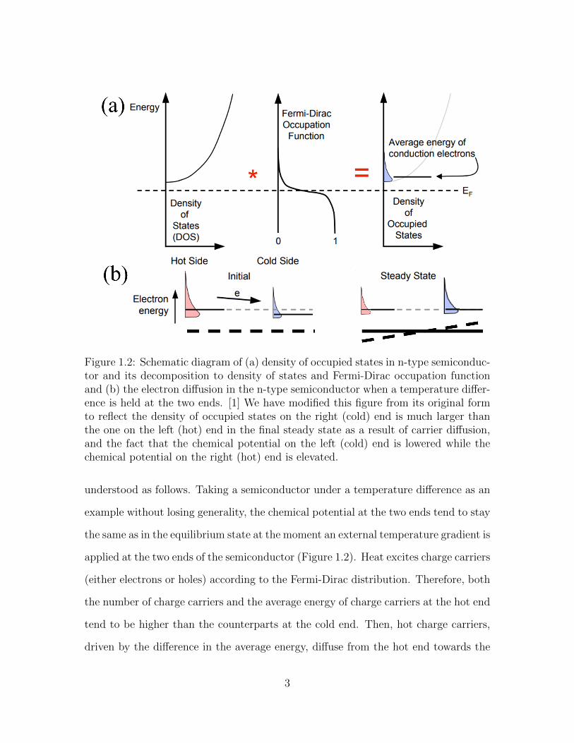
Figure 1.2: Schematic diagram of (a) density of occupied states in n-type semiconduc-tor and its decomposition to density of states and Fermi-Dirac occupation functionand (b) the electron diffusion in the n-type semiconductor when a temperature differ-ence is held at the two ends. [1] We have modified this figure from its original formto reflect the density of occupied states on the right (cold) end is much larger thanthe one on the left (hot) end in the final steady state as a result of carrier diffusion,and the fact that the chemical potential on the left (cold) end is lowered while thechemical potential on the right (hot) end is elevated.
understood as follows. Taking a semiconductor under a temperature difference as an
example without losing generality, the chemical potential at the two ends tend to stay
the same as in the equilibrium state at the moment an external temperature gradient is
applied at the two ends of the semiconductor (Figure 1.2). Heat excites charge carriers
(either electrons or holes) according to the Fermi-Dirac distribution. Therefore, both
the number of charge carriers and the average energy of charge carriers at the hot end
tend to be higher than the counterparts at the cold end. Then, hot charge carriers,
driven by the difference in the average energy, diffuse from the hot end towards the
3
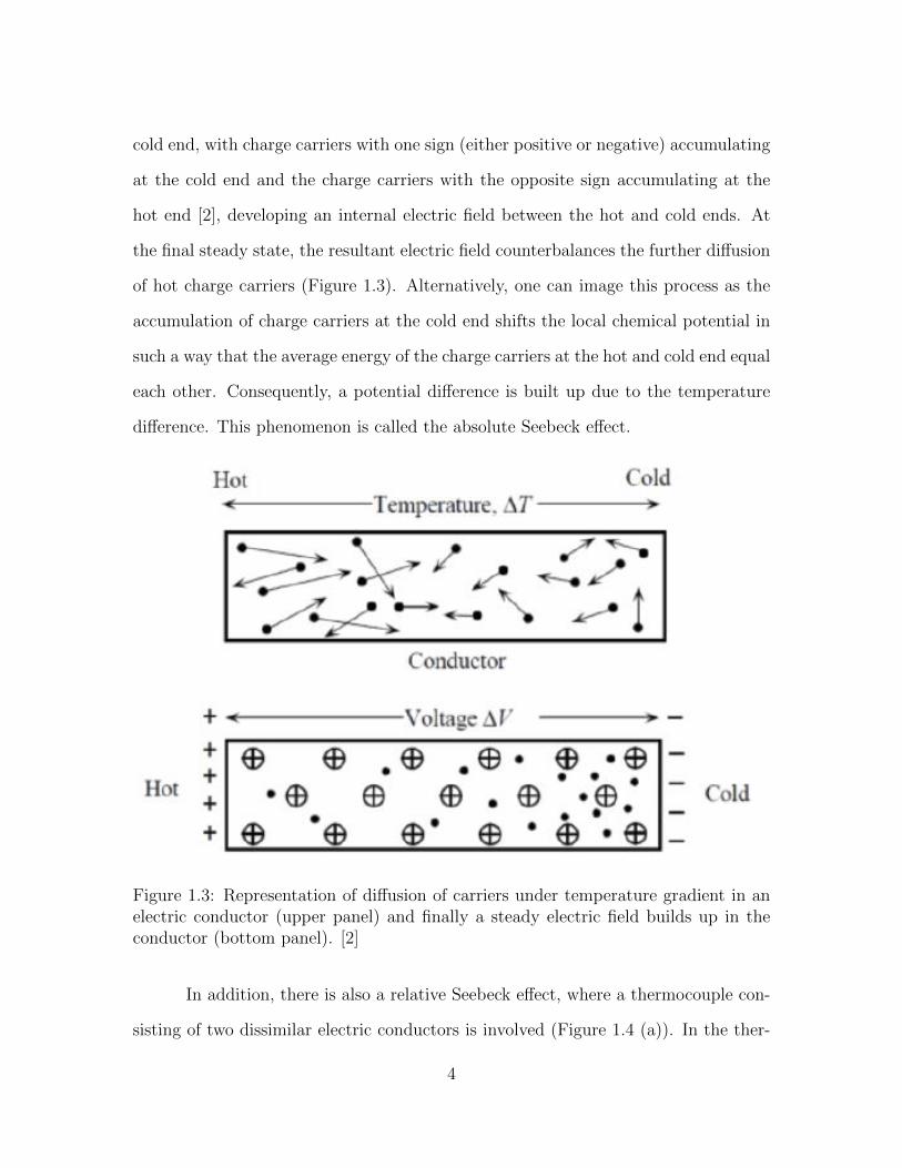
cold end, with charge carriers with one sign (either positive or negative) accumulating
at the cold end and the charge carriers with the opposite sign accumulating at the
hot end [2], developing an internal electric field between the hot and cold ends. At
the final steady state, the resultant electric field counterbalances the further diffusion
of hot charge carriers (Figure 1.3). Alternatively, one can image this process as the
accumulation of charge carriers at the cold end shifts the local chemical potential in
such a way that the average energy of the charge carriers at the hot and cold end equal
each other. Consequently, a potential difference is built up due to the temperature
difference. This phenomenon is called the absolute Seebeck effect.
Figure 1.3: Representation of diffusion of carriers under temperature gradient in anelectric conductor (upper panel) and finally a steady electric field builds up in theconductor (bottom panel). [2]
In addition, there is also a relative Seebeck effect, where a thermocouple con-
sisting of two dissimilar electric conductors is involved (Figure 1.4 (a)). In the ther-
4
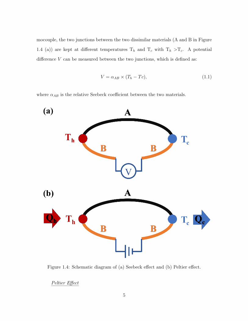
mocouple, the two junctions between the two dissimilar materials (A and B in Figure
1.4 (a)) are kept at different temperatures Th and Tc with Th >Tc. A potential
difference V can be measured between the two junctions, which is defined as:
V = αAB × (Th − Tc), (1.1)
where αAB is the relative Seebeck coefficient between the two materials.
Figure 1.4: Schematic diagram of (a) Seebeck effect and (b) Peltier effect.
Peltier Effect
5
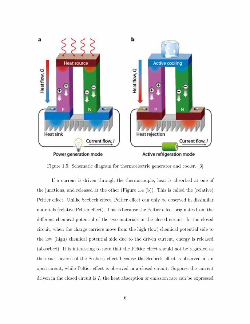
Figure 1.5: Schematic diagram for thermoelectric generator and cooler. [3]
If a current is driven through the thermocouple, heat is absorbed at one of
the junctions, and released at the other (Figure 1.4 (b)). This is called the (relative)
Peltier effect. Unlike Seebeck effect, Peltier effect can only be observed in dissimilar
materials (relative Peltier effect). This is because the Peltier effect originates from the
different chemical potential of the two materials in the closed circuit. In the closed
circuit, when the charge carriers move from the high (low) chemical potential side to
the low (high) chemical potential side due to the driven current, energy is released
(absorbed). It is interesting to note that the Peltier effect should not be regarded as
the exact inverse of the Seebeck effect because the Seebeck effect is observed in an
open circuit, while Peltier effect is observed in a closed circuit. Suppose the current
driven in the closed circuit is I, the heat absorption or emission rate can be expressed
6
as:
q = ΠABI (1.2)
where ΠAB is the relative Peltier coefficient similar to the relative Seebeck coeffi-
cient. It is obvious from Equation 1.2 that the heat absorption or emission rate is
proportional to the current driven through the closed circuit.
1.1.2 Thermoelectric Generator and Cooler
The Seebeck effect discussed above provides the foundation for a thermoelectric
generator. Figure 1.5(a) depict the schematic diagram of a thermoelectric generator
consisting of both n-type and p-type semiconductors (aka n- and p-thermoelectric
legs). When a temperature difference is maintained at the two junctions of two
thermoelectric legs, more electrons in the n-type semiconductor and more holes in
the p-type semiconductor are excited at the hot side. Under the influence of the
concentration gradient, the electrons (holes) in the n-leg (p-leg) would diffuse from
the hot side to the cold side, building a voltage difference between the two ends of
the generator.
Thermoelectric cooler, which can be regarded as the inverse of the thermoelec-
tric generator, is based on the Peltier effect. Similar to the thermoelectric generator,
a thermoelectric cooler also consists of n-legs and p-legs, which are connected electri-
cally in series and thermally in parallel. The schematic diagram for a thermoelectric
cooler is depicted in Figure 1.5 (b). When a current is driven through the closed
series loop, electrons in the n-legs would move in the direction opposite to that of the
applied current; in the meanwhile, holes in the p-legs would move in the same direc-
tion as the current. When the charge carriers move from one junction to the other,
energy carried by the charge carrier is released or absorbed depending on the average
7
energy of the charge carriers. As can be seen from Figure 1.5 (b), both electrons in
the n-legs and holes in the p-legs run away from the top junction towards the bottom
junction carrying heat with them, which finally results in the top junction cooled and
the bottom junction heated. It should be noted that if the current in Figure 1.5 (b)
is reversed, the cooling (heating) effect would occur at the top (bottom) junctions.
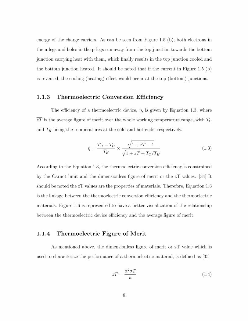
1.1.3 Thermoelectric Conversion Efficiency
The efficiency of a thermoelectric device, η, is given by Equation 1.3, where
zT is the average figure of merit over the whole working temperature range, with TC
and TH being the temperatures at the cold and hot ends, respectively.
η =TH − TCTH
×
√1 + zT − 1√
1 + zT + TC/TH(1.3)
According to the Equation 1.3, the thermoelectric conversion efficiency is constrained
by the Carnot limit and the dimensionless figure of merit or the zT values. [34] It
should be noted the zT values are the properties of materials. Therefore, Equation 1.3
is the linkage between the thermoelectric conversion efficiency and the thermoelectric
materials. Figure 1.6 is represented to have a better visualization of the relationship
between the thermoelectric device efficiency and the average figure of merit.
1.1.4 Thermoelectric Figure of Merit
As mentioned above, the dimensionless figure of merit or zT value which is
used to characterize the performance of a thermoelectric material, is defined as [35]
zT =α2σT
κ(1.4)
8
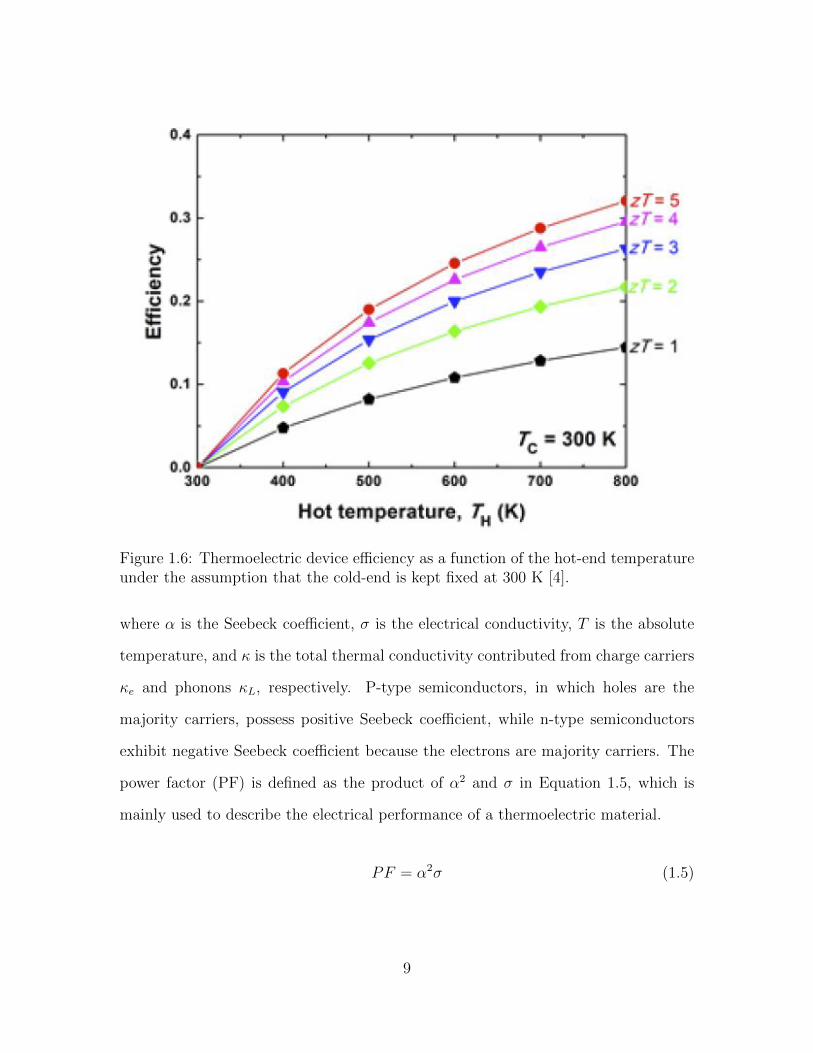
Figure 1.6: Thermoelectric device efficiency as a function of the hot-end temperatureunder the assumption that the cold-end is kept fixed at 300 K [4].
where α is the Seebeck coefficient, σ is the electrical conductivity, T is the absolute
temperature, and κ is the total thermal conductivity contributed from charge carriers
κe and phonons κL, respectively. P-type semiconductors, in which holes are the
majority carriers, possess positive Seebeck coefficient, while n-type semiconductors
exhibit negative Seebeck coefficient because the electrons are majority carriers. The
power factor (PF) is defined as the product of α2 and σ in Equation 1.5, which is
mainly used to describe the electrical performance of a thermoelectric material.
PF = α2σ (1.5)
9
1.2 Experimental Efforts to Explore High Figure
of Merit
1.2.1 Optimizing the Carrier Concentration
All the physical quantities except κL in Equation 1.4 are coupled to each other
as functions of carrier concentration, n. n is governed by the doping level, temper-
ature, and defects. In general, the electrical conductivity increases as the carrier
concentration increases. On the contrary, the Seebeck coefficient decreases with in-
crease of the carrier concentration (Figure 1.7). As a result, there is no ideal method
to optimize these quantities (except κL) separately. However, according to Figure
1.7, through optimizing the carrier concentration, it is possible that the power factor
reaches an optimal value. The optimal carrier concentration of different thermo-
electric materials differs from each other. However, it generally falls in the range
1018-1020 cm−3, which usually belongs to the range for the degenerate semiconduc-
tors. [35] Therefore, to optimize the power factor requires doping, alloying or other
strategies to tune the carrier concentration. In addition, it is verified in Bi2Te3 that
it is possible to tune the intrinsic point defect in Bi2Te3 through extrinsic doping,
which in turn helps optimize the carrier concentration. [36]
However, it should be noted that the optimal carrier concentration for zT and
power factor is different, which is due to that the optimal carrier concentration for
power factor benefits not only the electrical performance but also the electrical ther-
mal conductivity. With increasing electrical thermal conductivity, the total thermal
conductivity is also elevated, negatively affecting the final zT. Therefore, the optimal
carrier concentration for maximum zT should be slightly lower that corresponding to
the maximum power factor.
10

Figure 1.7: Relationship between the electrical transport properties (Seebeck coeffi-cient, electrical conductivity, and power factor) and the carrier concentration [5].
1.2.2 Band Engineering
At a fixed carrier concentration, it is possible to further optimize the thermo-
electric performance via band engineering. According to Equation 1.6,
α =8π2
3
k2BT
eh2m∗(
π
3n)23 (1.6)
the Seebeck coefficient is not only determined by the carrier concentration but also
proportional to the density of state (DOS) effective mass, indicating increasing the
DOS effective mass of charge carrier, the Seebeck coefficient could be elevated. As
can be seen from the DOS effective mass expression m∗ = N2/3v m∗b [6, 37], where Nv is
the band valley degeneracy and m∗b is the band effective mass, that increasing Nv or
m∗b could increase the DOS effective mass, thus further optimizing the thermoelectric
11
performance. On the other hand, it should be noted that if the charge carrier is
mainly scattered by phonons, which is usually the case for thermoelectric materials
especially at high temperatures, the charge carrier and the band effective mass has
a relation µ ∝ 1/m∗b5/2 [6, 37]. In the meanwhile, according to the Drude model,
σ = nqµ, at a fixed carrier concentration, the carrier mobility is determinant for
the electrical conductivity. Therefore, increasing the band effective mass must be
accompanied by sacrificing the electrical conductivity and thus the thermoelectric
performance. Compared to increasing the band effective mass, increasing the band
valley degeneracy is more effective method to enhancing the DOS effective mass [38].
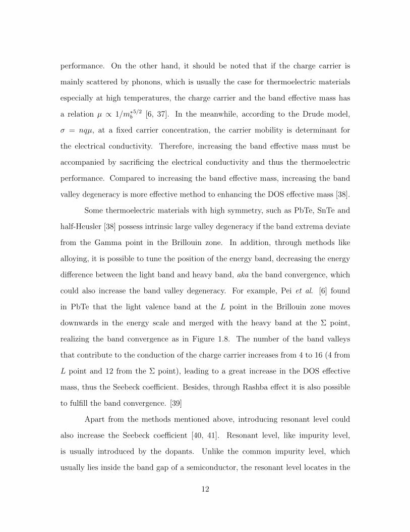
Some thermoelectric materials with high symmetry, such as PbTe, SnTe and
half-Heusler [38] possess intrinsic large valley degeneracy if the band extrema deviate
from the Gamma point in the Brillouin zone. In addition, through methods like
alloying, it is possible to tune the position of the energy band, decreasing the energy
difference between the light band and heavy band, aka the band convergence, which
could also increase the band valley degeneracy. For example, Pei et al. [6] found
in PbTe that the light valence band at the L point in the Brillouin zone moves
downwards in the energy scale and merged with the heavy band at the Σ point,
realizing the band convergence as in Figure 1.8. The number of the band valleys
that contribute to the conduction of the charge carrier increases from 4 to 16 (4 from
L point and 12 from the Σ point), leading to a great increase in the DOS effective
mass, thus the Seebeck coefficient. Besides, through Rashba effect it is also possible
to fulfill the band convergence. [39]
Apart from the methods mentioned above, introducing resonant level could
also increase the Seebeck coefficient [40, 41]. Resonant level, like impurity level,
is usually introduced by the dopants. Unlike the common impurity level, which
usually lies inside the band gap of a semiconductor, the resonant level locates in the
12
conduction band or valence band depending on the type of dopants. Accordingly, the
DOS shows a spike, which is beneficial in increasing the DOS effective mass. Typical
examples include Tl doped PbTe [42], Al doped PbSe [43] and In doped SnTe [44],
etc.
1.2.3 Efforts to Decrease Lattice Thermal Conductivity
As mentioned above, lattice thermal conductivity is the factor that could be de-
coupled from the electrical transport parameters, which could be optimized separately.
In recent years, more and more methods to reducing the lattice thermal conductivity
have been reported. For example, the multi-scale scattering center introduced by
defect engineering could help shorten the phonon mean free path [45], thus decreas-
ing the lattice thermal conductivity. From the dimensional viewpoint, in general,
defects can be categorized into zero-dimensional (point defect), one-dimensional (dis-
location), two-dimensional (grain boundary) and three-dimensional (nano inclusion
or secondary phase) [46]. Point defect, including vacancy [47, 48], doping or alloying
[49] and interstitial atoms [50], can scatter high-frequency phonon effectively. High
density dislocation can scatter mid-frequency phonons, which can be introduced via
plastic deformation of the samples. Large amount of grain boundaries can be in-
troduced via grain refinement and nano-structuring, thus forming high density grain
boundary scattering centers, which can scatter low-frequency phonons. However, it
should be noted that the high density grain boundary scattering center not only scat-
ters the low-frequency phonon but the charge carriers, which has negative effect on
the electrical performance. Introducing the above discussed defects into one sample,
we can construct multi-frequency and multi-scale scattering centers, thus realizing
the reduction of lattice thermal conductivity. For instance, Biswas et al. introduced
13
the multi-scale scattering centers into PbTe and achieved a zT around 2.2 at 915 K
[51].
In addition, the lattice thermal conductivity can also be effectively reduced
via lattice anharmonicity [52], complex crystal structure[53], porous structure [54, 55],
and introducing heavy element or weak chemical bonding [56].
1.2.4 Pre-screening Factor
It can be inferred from the discussion above that to explore the high perfor-
mance thermoelectric materials, there are large amounts of work to be done experi-
mentally due to the large phase space for the parent compounds to be dealt with, not
to mention the fine-tuning of the electrical and thermal transport properties via dop-
ing or alloying. To reduce the size of the phase space, experimentalists came up with
some pre-screening factor for excellent thermoelectric materials, such as degenerate
semiconductors with carrier concentration between 1018 and 1020 cm−3, semiconduc-
tors with small band gap, high symmetry crystal structure, small electronegativity
difference among the constituent element, etc.
However, even with the pre-screening factors, to enumerate all the possible case
in the large phase space or to fast-target some promising candidates for thermoelectric
application is a great burden from the experimental point of view. Therefore, more
advanced techniques should be developed not only in the vein of experiment but also
the path along the theoretical efforts.
14
1.3 Calculations of the Thermoelectric Figure of
Merit
The calculations of the thermoelectric figure of merit involves two parts: (i)
the electrical transport properties, such Seebeck coefficient, electrical conductivity
and electrical thermal conductivity; (ii) the phonon transport properties (aka lattice
thermal conductivity). Solving the phonon Boltzmann transport equation (BTE) is
an easy but efficient way to calculate both the electrical transport properties and
phonon transport properties.
1.3.1 Phonon Transport Properties
In the presence of a temperature gradient ∇T , the Bose-Einstein distribution
of a phonon mode, f , deviates from f 0, and this deviation can be obtained from the
BTE. The phonon distribution function is influenced by both the diffusion due to
the temperature gradient and the scattering from possible scattering processes, such
as phonon-phonon scattering, phonon-isotope scattering, electron-phonon scattering,
etc. For a steady state, the changing rate of the phonon distribution function must
vanish, which can be expressed by the BTE [57, 58]:
−vqp · ∇T∂fqp∂T
+∂fqp∂t|scatt = 0 (1.7)
where q and p represent the wave vector and phonon band branch of a phonon mode.
In the following, we will use λ to denote the phonon mode with wave vector q and
phonon band branch p. vλ is the phonon group velocity. In Equation 1.7, the first
term is the temperature gradient induced diffusion term, and the second term is the
scattering processes governed scattering term. Under a small temperature gradient,
15
the phonon BTE can be linearized with fλ = f 0λ + f 0
λ(1 + f 0λ)Φλ, where Φλ is a small
perturbation. If only three-phonon processes within the phonon-phonon scattering
are considered for the scattering term, the linearized phonon BTE can be written as
[59, 60]
−vλ·∇T∂f 0
λ
∂T=f 0λ (1 + f 0
λ)
N×∑λ′λ′′
[(Φλ + Φλ′ − Φλ′′) Γ+
λλ′λ′′ +1
2(Φλ − Φλ′ − Φλ′′) Γ−λλ′λ′′
](1.8)
where a discretization of the Brillouin zone into a Gamma-point-centered regular grid
of N = N1×N2×N3 q points is employed, with N1, N2 and N3 being the number of
divisions along the three principal axes in the Brillouin zone. Γ+λλ′λ′′ and Γ−λλ′λ′′ are the
transition rates due to the three phonon absorption (+) and emission (-) processes,
respectively, which can be calculated directly from first principles. [61, 62, 63, 64, 65]
With the phonon BTE solved and the distribution function f obtained, it is
then possible to calculate the lattice thermal conductivity. The detailed methods are
provided in Chapter 2.
1.3.2 Electrical Transport Properties
Similar to the phonon transport properties, in the presence of an external elec-
tric field E, the Fermi-Dirac distribution of an electronic state, f , deviates from its
equilibrium distribution f 0, and this deviation can be calculated using the electron
BTE. The electron distribution function is affected by the diffusion due to the ex-
ternal electric field, and the scattering from possible scattering processes, which is
mainly governed by the electron-phonon interaction for single crystal samples at high
temperature. When the external electric field E is small, the BTE for the electrical
16
transport properties has the form:
−qEh
∂fnk∂k
+∂fnk∂t|scatt = 0 (1.9)
where q is the elementary charge, h is the reduced Planck constant, E is the external
electric field, fnk is the electron distribution function with electron wave vector k and
band branch n.
Compared to the full solution to the phonon BTE, the development of the
solution to the electron BTE falls behind. Nowadays, the common way to deal with
the scattering term (the second term on the left of Equation 1.9) in the electron BTE
is to use the constant relaxation time approximation with the form:
∂fnk∂t|scatt =
fnk − f 0nk
τ(1.10)
where τ is the relaxation time. It should be pointed out that the relaxation time is
identical for different electronic state under the constant relaxation time approxima-
tion, which is physically meaningless. In addition, despite the relaxation time could
be fit from experimental data or using some empirical expressions, this type of solu-
tion to the electron BTE lacks the predictive power. Therefore, the calculations of the
electrical transport properties based on the constant relaxation time approximation
could only provide phenomenological explanations to the experimental results, which
is also the main reason why there is much less computational research work in the
thermoelectric field than the experimental work. In order to make the calculations of
the electrical transport properties fully from first principles, more advanced solution
to the electron BTE is in high demand.
17
1.4 Electron-phonon interactions
The electron-phonon interactions, where an electron exchanges energy and
momentum with phonons (collective modes of the lattice vibrations), play a key role
in condensed matter physics and materials science and engineering. For example, the
electron-phonon interaction is responsible for the fundamental physical phenomena
such as the conventional superconductivity [66], Kohn anomaly [67] and the Peierls
[68] distortions, etc. The broadening of the spectral lines in angle-resolved photoemis-
sion spectroscopy [69] and in vibrational spectroscopy [70], phonon-assisted photon
absorption [71, 72, 73] as well as for the temperature dependence of the band gaps in
semiconductors [74] are consequences of the interactions between electrons and lattice
vibrations.
Most important to this dissertation is that electrical conductivity and related
electrical transport properties [75] have a close relation with the electron-phonon
interactions. Thus, the electron-phonon interaction also plays an important role in
the thermoelectric effect [76]. According to the first order perturbation theory, an
electron can change its state by absorbing or emitting a phonon, corresponding to
the phonon absorption process and phonon emission process, respectively. According
to the Fermi golden rule, it is possible to calculate the scattering rate of each process
for each electronic state. The obtained scattering rates for each electronic state can
then be fed into the electron BTE, which is the advanced first principles solution to
the electron BTE we desire. Finally, it is possible to calculate the electron-phonon
interaction limited electrical transport properties under the framework of BTE and
electron-phonon interaction. The detailed methodology is presented in Chapter 2.
18

Figure 1.8: Relative energy of the valence bands in PbTe0.85Se0.15. At around 500 Kthe two valence bands converge, resulting in transport contributions from both the Land S bands. C denotes conduction band; L represents low degeneracy hole band; S ishigh degeneracy hole band. [6]. It should be noted that in the figure, only the relativeshift of the band extrema makes sense since in reality it is impossible to rigidly shiftthe whole band.
19

Chapter 2
First Principles Methods for
Electrical and Phonon Transport
Calculations
2.1 Electrical Transport Properties
Recall the expression for the electron BTE:
−qEh
∂fnk∂k
+∂fnk∂t|scatt = 0 (2.1)
where q is elementary charge and h is the reduced Planck constant. If the external
electric field E is small (low-field limit), fnk could be expressed using Taylor expansion
as fnk = f 0nk + fnk(1− fnk)Φnk, with Φnk being a small perturbation which is linear
with respect to E. Therefore, it is convenient to express Φnk as qEkBT·Fnk, with kB being
the Boltzmann constant, and T being the temperature. Fnk can be considered as the
mean free displacement [58, 77]. If the scattering term (second term) of Equation 2.1
20
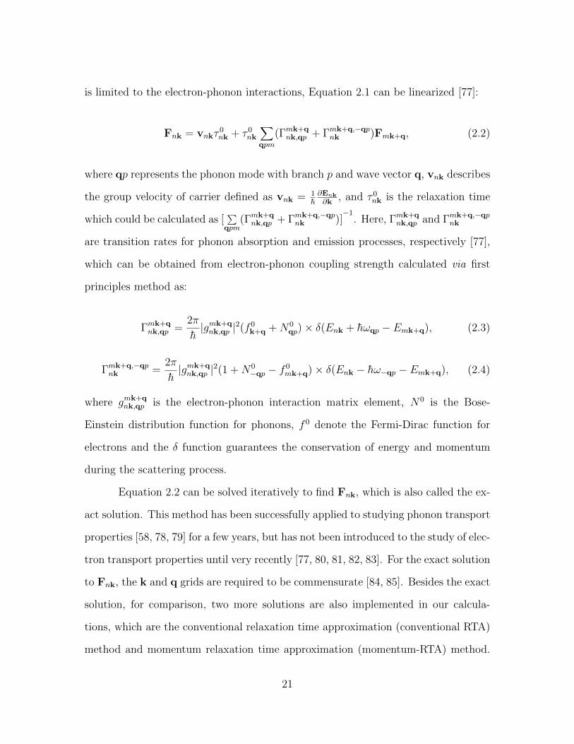
is limited to the electron-phonon interactions, Equation 2.1 can be linearized [77]:
Fnk = vnkτ0nk + τ 0
nk
∑qpm
(Γmk+qnk,qp + Γmk+q,−qp
nk )Fmk+q, (2.2)
where qp represents the phonon mode with branch p and wave vector q, vnk describes
the group velocity of carrier defined as vnk = 1h∂Enk∂k
, and τ 0nk is the relaxation time
which could be calculated as [∑qpm
(Γmk+qnk,qp + Γmk+q,−qp
nk )]−1
. Here, Γmk+qnk,qp and Γmk+q,−qp
nk
are transition rates for phonon absorption and emission processes, respectively [77],
which can be obtained from electron-phonon coupling strength calculated via first
principles method as:
Γmk+qnk,qp =
2π
h|gmk+qnk,qp |2(f 0
k+q +N0qp)× δ(Enk + hωqp − Emk+q), (2.3)
Γmk+q,−qpnk =
2π
h|gmk+qnk,qp |2(1 +N0
−qp − f 0mk+q)× δ(Enk − hω−qp − Emk+q), (2.4)
where gmk+qnk,qp is the electron-phonon interaction matrix element, N0 is the Bose-
Einstein distribution function for phonons, f 0 denote the Fermi-Dirac function for
electrons and the δ function guarantees the conservation of energy and momentum
during the scattering process.
Equation 2.2 can be solved iteratively to find Fnk, which is also called the ex-
act solution. This method has been successfully applied to studying phonon transport
properties [58, 78, 79] for a few years, but has not been introduced to the study of elec-
tron transport properties until very recently [77, 80, 81, 82, 83]. For the exact solution
to Fnk, the k and q grids are required to be commensurate [84, 85]. Besides the exact
solution, for comparison, two more solutions are also implemented in our calcula-
tions, which are the conventional relaxation time approximation (conventional RTA)
method and momentum relaxation time approximation (momentum-RTA) method.
21
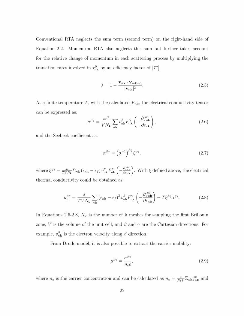
Conventional RTA neglects the sum term (second term) on the right-hand side of
Equation 2.2. Momentum RTA also neglects this sum but further takes account
for the relative change of momentum in each scattering process by multiplying the
transition rates involved in τ 0nk by an efficiency factor of [77]
λ = 1− vnk · vmk+q
|vnk|2. (2.5)
At a finite temperature T , with the calculated Fnk, the electrical conductivity tensor
can be expressed as:
σβγ =se2
V Nk
∑nk
vβnkFγnk
(−∂f
0nk
∂εnk
), (2.6)
and the Seebeck coefficient as:
αβγ =(σ−1
)βηξηγ, (2.7)
where ξηγ = seTV Nk
Σnk (εnk − εf ) vηnkFγnk
(−∂f0nk∂εnk
). With ξ defined above, the electrical
thermal conductivity could be obtained as:
κβγe =s
TV Nk
∑nk
(εnk − εf )2 vβnkFγnk
(−∂f
0nk
∂εnk
)− Tξβηαηγ, (2.8)
In Equations 2.6-2.8, Nk is the number of k meshes for sampling the first Brillouin
zone, V is the volume of the unit cell, and β and γ are the Cartesian directions. For
example, vβnk is the electron velocity along β direction.
From Drude model, it is also possible to extract the carrier mobility:
µβγ =σβγ
nce, (2.9)
where nc is the carrier concentration and can be calculated as nc = sNkV
Σnkf0nk and
22
nc = sNkV
Σnk(1− f 0nk) for n-type and p-type semiconductors, respectively.
2.2 Lattice Thermal Conductivity
In the linearized phonon BTE in mentioned in Chapter 1 (Equation 1.7), it
should be noted that the conservation of both energy (ωλ±ωλ′ = ωλ′′) and momentum
(qλ ± qλ′ = qλ′′ + G) must be obeyed in all the allowed scattering processes, where
+ and - are for absorption and emission processes, respectively, and G is a reciprocal
lattice vector. In absorption processes, a phonon λ is scattered by absorbing a phonon
λ′ to yield a third phonon λ′′; while in emission processes, a phonon λ decays into
two phonons λ′ and λ′′. Γ+λλ′λ′′ and Γ−λλ′λ′′ can be expressed as [58]:
Γ+λλ′λ′′ =
hπ
4(f 0λ′ − f 0
λ′′)× |V +λλ′λ′′‖2 × δ(ωλ + ωλ′ − ωλ′′)
ωλωλ′ωλ′′, (2.10)
Γ−λλ′λ′′ =hπ
4(f 0λ′ + f 0
λ′′ + 1)× |V −λλ′λ′′ |2 ×δ(ωλ − ωλ′ − ωλ′′)
ωλωλ′ωλ′′, (2.11)
where
V +λλ′λ′′ =
∑bl′b′l′′b′′
∑αβγ Φαβγ
0b,l′b′,l′′b′′eλαbe
λ′βb′e
−λ′′γb′′√
mbmb′mb′′× e+iq′·rl′e−iq
′′·rl′′ , (2.12)
V −λλ′λ′′ =
∑bl′b′l′′b′′
∑αβγ Φαβγ
0b,l′b′,l′′b′′eλαbe−λ′βb′ e−λ
′′
γb′′√mbmb′mb′′
× e−iq′·rl′e−iq′′·rl′′ . (2.13)
V +λλ′λ′′ and V −λλ′λ′′ are the scattering matrix elements for absorption and emission
processes, respectively. Since Φλ is linear with ∇T , we can write Φλ = − hωλkBT 2 Fλ ·∇T ,
where Fλ can be regarded as mean free displacement, a generalization of mean free
path [58], and ωλ is the angular frequency. To simplify the linearized phonon BTE
23
equation (Equation 1.8), we further define Eλ ≡ ωλFλ, and can obtain
{−ωλvλ +
1
N
∑λ′λ′′
[(Eλ + Eλ′ − Eλ′′)Γ+λλ′λ′′ +
1
2(Eλ − Eλ′ − Eλ′)Γ
−λλ′λ′′ ]
}· ∇T = 0.
(2.14)
Taking Eλ out of the summation term in Equation 2.14, we obtain its iterative form
as
Ei+1λ = E0
λ +τ 0λ
N
∑λ′λ′′
[(Eiλ′′ − Ei
λ′)Γ+λλ′λ′ +
1
2(Ei
λ′′ + Eiλ′)Γ
−λλ′λ′ ], i = 1, 2, 3, ...... (2.15)
where N is the number of sampled q-points in the reciprocal space. The iterative
process starts with
E0λ = ωλvλτ
0λ (2.16)
with 1τ0λ
= 1N
∑λ′λ′′(Γ
+λλ′λ′′ + 1
2Γ−λλ′λ′′). Notice it is also possible to include the phonon-
isotope scattering the in expression for τ 0λ using Matthiessen’s rule, which is discussed
in the Appendix A. In fact, setting Eλ equal to E0λ is equivalent to the conventional
RTA solution to the linearized phonon BTE (Equation 1.8) [58]. The process is
regarded as converged when the difference between the values of Eλ in two consecu-
tive steps is below a convergence threshold. The Eλ should converge for all phonon
modes in the iterative process, which is too slow from the computational point of
view. Instead, the convergence criterion for κL is implemented [58]. When the devi-
ation between the values of κL in two consecutive steps falls within the convergence
threshold, the iteration scheme is terminated.
The heat current J generated from the small temperature gradient can be
expressed in terms of the distribution function fλ or Eλ in the linearized BTE (2.14))
24
[60, 86],
J =1
NV
∑λ
hωλvλfλ = − 1
kBT 2NV
∑λ
h2ωλf0λ
(1 + f 0
λ
)vλ (Eλ · ∇T ) (2.17)
where V is the volume of the unit cell, and we have used the fact the heat current
is vanishing at the equilibrium state. From Fourier’s law Jα = −∑β καβ(∇T )β, it
follows
καβ =1
kBT 2NV
∑λ
h2ωλf0λ(1 + f 0
λ)v0λE
βλ . (2.18)
25
Chapter 3
Carrier Scattering Mechanism in
3C-SiC
We have developed the first principles methods for the calculations of electrical
transport properties in Chapter 2, whose accuracy still needs further examination.
In this chapter, we used 3C-SiC as an example to validate our methods for obtaining
the electrical transport properties such as carrier mobility. Despite there are only
two atoms inside the primitive unit cell of 3C-SiC, the two atoms belong to different
elements, leading 3C-SiC to be a polar semiconductor, which is ideal to examine
the accuracy of the interpolated electron-phonon interaction matrix elements with
the polar-longitudinal-optical phonons. Also, the simple crystal structure that 3C-
SiC possesses makes the calculations of the electrical transport properties limited
by the electron-phonon interaction less expensive. In addition, there are abundant
experimental data measured on the single crystal samples available for both n-type
and p-type 3C-SiC, which makes it easy to compare our calculated electrical transport
properties, such as the carrier mobility, to the available experimental data.
26
3.1 Introduction
Silicon carbide (SiC) is one of the most promising alternatives to silicon for
high-temperature and/or high-power devices because of its unique combination of
wide band gap [87, 88],high breakdown voltage [87, 88], and high thermal conduc-
tivity [89, 90]. The performance of SiC-based devices has been demonstrated in past
decades [91, 92, 93, 94, 95, 96, 97]. From a fundamental research point of view, SiC is
interesting in its own right. For example, SiC has numerous allotropes, among which
the cubic phase (3C) and hexagonal phases (4H and 6H) are the most interesting.
Note that the device applications of SiC rely on its electrical transport properties.
Concerning the electrical transport properties, the 4H and 3C phases have been re-
ported to have substantially higher electron mobility than the 6H phase [98]. In
particular, 3C-SiC adopts a simple zinc-blende crystal structure, which is isotropic,
with several advantages compared to other allotropes with respect to applications.
Despite the abundant data in literature, both experimental [9, 10, 99, 100] and
theoretical [101, 102, 103, 104, 105, 106, 107, 108], the electrical transport properties of
3C-SiC have not yet been fully understood at the microscopic level. The experimental
electron mobilities vary greatly from sample to sample, intimately related to the
quality and growth conditions. For example, Nelson et al. [9] reported a room
temperature electron mobility of 890 cm2/V · s in n-type single crystalline 3C-SiC.
Shinohara et al. [10] obtained a value larger than 750 cm2/V · s in undoped 3C-SiC
epitaxial film grown on carbonized silicon surfaces. Yamanaka et al. [99] obtained a
much smaller value around 500 cm2/V · s for incidentally doped n-type 3C-SiC layers
epitaxially grown on silicon, and the authors argued that longitudinal acoustic (LA)
phonons dominate the scattering mechanism at room temperature and above. On the
theory side, a value of 1300 cm2/V ·s at 300 K has been reported which assumes polar
27
longitudinal optical (LO) phonon scattering being the dominant scattering mechanism
[108]. These early studies focused mainly on n-type 3C-SiC, however, the research
on p type 3C-SiC is scarce. Thus, there is a knowledge gap regarding p-type 3C-
SiC, preventing us from obtaining a coherent and complete picture of the electrical
transport properties of 3C-SiC.
As discussed above, electron-phonon interaction is at the core of understand-
ing the electrical transport properties of 3C-SiC at the microscopic level. To this end,
first-principles calculations of carrier transport properties are the tools of choice to fill
this gap of knowledge. However, first-principles calculations of carrier transport prop-
erties are computationally expensive as very dense meshes of Brillouin zone sampling
are required for both carriers and phonons. The lately developed interpolation meth-
ods for electron-phonon interaction matrix elements [77, 84, 85, 109] greatly reduced
the time required for calculating the electron-phonon interaction matrix elements.
The efficiency of these methods has been confirmed in both nonpolar materials and
polar materials [77, 80, 81, 83, 110, 111, 112]. Therefore, in this paper, we carry out
first-principles calculations to have a deeper understanding of the intrinsic electron
and hole transport mechanism of single crystalline 3C-SiC. In particular, the Wan-
nier function interpolation method [84, 85, 109, 113] 29313233is employed to obtain
the electron-phonon interaction matrix elements, which are then used to calculate
phonon-limited scattering rates and carrier mobilities by solving the electron BTE
(Equation 2.1).
3.2 Computational Details
Density functional theory (DFT) is employed to calculate the geometric struc-
ture and electronic band structure, while density functional perturbation theory is
28
used to obtain phonon dispersion relation and initial electron-phonon interaction
matrix elements as implemented in Quantum Espresso package [114] with norm-
conserving pseudopotential under the local density approximation [115]. The planewave
cutoff energy is set to be 58 Ry, and 16 × 16 × 16 Monkhorst-Pack k meshes are used
for structure relaxation, both of which are well converged. The lattice structure of
3C-SiC is shown in Figure 3.1(a) with the relaxed lattice constant of 4.326 A, agree-
ing well with experimental value 4.360 A[116]. To interpolate the electron-phonon
interaction matrix elements, the EPW package [85] is employed to perform Wannier
function interpolation. The initial coarse grids are chosen as 6 × 6 × 6 for both k and
q. The chemical potential is manually chosen to be 0.3 eV in the band gap away from
the band edges to ensure that the calculated mobility is intrinsically phonon-limited
and corresponds to a low carrier concentration limit, where the defect scattering can
be ignored.
3.3 Results and Discussions
It has been reported that the spin orbit coupling (SOC) effect, which leads to
the splitting of the degenerate valence band, has a great influence on the hole mobility
in different materials [81, 82, 83]. Therefore, in our calculation, SOC is included for
the calculation of electronic band structure, phonon dispersion relation, and electron-
phonon interaction matrix elements unless otherwise stated. The electronic band
structure along high-symmetry paths [Figure 3.1](b) is shown in Figure 3.2(a). 3C-
SiC has an indirect band gap, with the valence band maximum (VBM) located at Γ
point, and the conduction band minimum (CBM) sitting at X point. The calculated
band gap is 1.34 eV, smaller than the experimental value of 2.42 eV [117]. This is a
result of DFT usually underestimating the energy of band gaps. However, the band
29
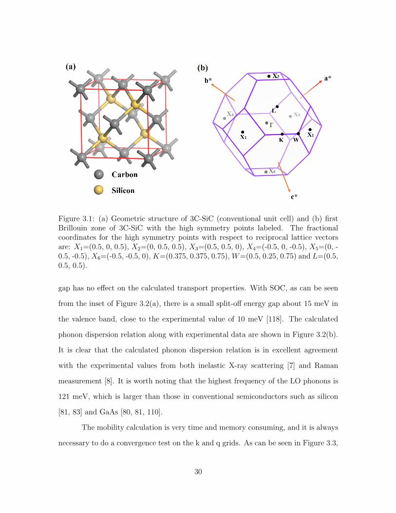
Figure 3.1: (a) Geometric structure of 3C-SiC (conventional unit cell) and (b) firstBrillouin zone of 3C-SiC with the high symmetry points labeled. The fractionalcoordinates for the high symmetry points with respect to reciprocal lattice vectorsare: X1=(0.5, 0, 0.5), X2=(0, 0.5, 0.5), X3=(0.5, 0.5, 0), X4=(-0.5, 0, -0.5), X5=(0, -0.5, -0.5), X6=(-0.5, -0.5, 0), K=(0.375, 0.375, 0.75), W=(0.5, 0.25, 0.75) and L=(0.5,0.5, 0.5).
gap has no effect on the calculated transport properties. With SOC, as can be seen
from the inset of Figure 3.2(a), there is a small split-off energy gap about 15 meV in
the valence band, close to the experimental value of 10 meV [118]. The calculated
phonon dispersion relation along with experimental data are shown in Figure 3.2(b).
It is clear that the calculated phonon dispersion relation is in excellent agreement
with the experimental values from both inelastic X-ray scattering [7] and Raman
measurement [8]. It is worth noting that the highest frequency of the LO phonons is
121 meV, which is larger than those in conventional semiconductors such as silicon
[81, 83] and GaAs [80, 81, 110].
The mobility calculation is very time and memory consuming, and it is always
necessary to do a convergence test on the k and q grids. As can be seen in Figure 3.3,
30

Figure 3.2: (a) Electronic band structure and (b) phonon dispersion relation alonghigh-symmetry points in the first Brillouin zone. Inset: zoom-in of the valence band,where the split-off gap is significantly clearer. Experimental data for phonon dis-persion are taken from Ref [7] and Ref [8]. Different branches: transverse acoustic(TA1 and TA2), longitudinal acoustic (LA), transverse optical (TO1 and TO2), andlongitudinal optical (LO) are depicted in different colors.
at room temperature, the obtained mobilities of holes and electrons are well converged
with the relative difference around 2% when the fine k and q meshes are both 120 ×
120 × 120.
With the converged k and q meshes mentioned above, the calculated carrier
mobilities as a function of temperature are depicted in Figure 3.4. For both electrons
and holes, the mobilities obtained with exact solution to the BTE (labeled as ITER
in Figure 3.4) agree very well with the experimental results in a broad temperature
range, from 200 K to 600 K. However, the conventional-RTA method strongly under-
estimates the mobilities by more than 31% and 17% variance for electrons and holes,
respectively.
Mobilities obtained without SOC are also plotted in Figure 3.4 for comparison.
Since SOC does not affect the conduction bands in 3C-SiC, the electron mobilities
calculated with and without SOC are identical. On the other end, calculation without
SOC slightly overestimates the hole mobilities compared to the valued obtained with
SOC. For example, at 300 K, the mobilities obtained with and without SOC effect
31
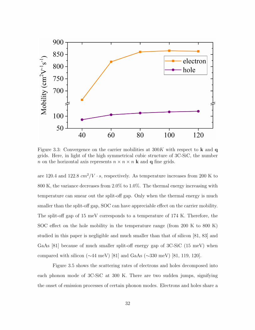
Figure 3.3: Convergence on the carrier mobilities at 300K with respect to k and qgrids. Here, in light of the high symmetrical cubic structure of 3C-SiC, the numbern on the horizontal axis represents n× n× n k and q fine grids.
are 120.4 and 122.8 cm2/V · s, respectively. As temperature increases from 200 K to
800 K, the variance decreases from 2.0% to 1.0%. The thermal energy increasing with
temperature can smear out the split-off gap. Only when the thermal energy is much
smaller than the split-off gap, SOC can have appreciable effect on the carrier mobility.
The split-off gap of 15 meV corresponds to a temperature of 174 K. Therefore, the
SOC effect on the hole mobility in the temperature range (from 200 K to 800 K)
studied in this paper is negligible and much smaller than that of silicon [81, 83] and
GaAs [81] because of much smaller split-off energy gap of 3C-SiC (15 meV) when
compared with silicon (∼44 meV) [81] and GaAs (∼330 meV) [81, 119, 120].
Figure 3.5 shows the scattering rates of electrons and holes decomposed into
each phonon mode of 3C-SiC at 300 K. There are two sudden jumps, signifying
the onset of emission processes of certain phonon modes. Electrons and holes share a
32
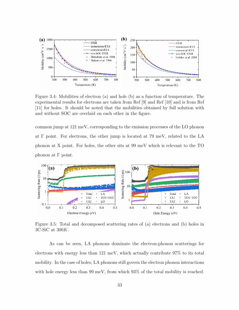
Figure 3.4: Mobilities of electron (a) and hole (b) as a function of temperature. Theexperimental results for electrons are taken from Ref [9] and Ref [10] and is from Ref[11] for holes. It should be noted that the mobilities obtained by full solution withand without SOC are overlaid on each other in the figure.
common jump at 121 meV, corresponding to the emission processes of the LO phonon
at Γ point. For electrons, the other jump is located at 79 meV, related to the LA
phonon at X point. For holes, the other sits at 99 meV which is relevant to the TO
phonon at Γ point.
Figure 3.5: Total and decomposed scattering rates of (a) electrons and (b) holes in3C-SiC at 300K.
As can be seen, LA phonons dominate the electron-phonon scatterings for
electrons with energy less than 121 meV, which actually contribute 97% to its total
mobility. In the case of holes, LA phonons still govern the electron phonon interactions
with hole energy less than 99 meV, from which 93% of the total mobility is reached.
33

This indicates that the LA phonon scattering is the governing scattering mechanism
in 3C-SiC at 300 K, in consistent with experimental observation [99, 121]. This is,
however, in contrast to other polar materials, such as GaAs [80, 81], PbTe [122],
SnSe [111], and SnTe [112], in which polar LO phonons dominate the scattering for
a wide energy range including band edges. Actually, LO-phonon scattering increases
suddenly by two orders of magnitude at 121 meV due to the occurrence of phonon
emission processes. As a result, LO phonons dominate the scattering above 121
meV. To understand the orders-of-magnitude smaller scattering below 121 meV for
the LO-phonon absorption processes, we refer to Equations 2.3 and 2.4. Since the
electron/hole occupation number can be neglected in the intrinsic limit, the scattering
rates from phonon absorption and emission processes are proportional to Nqp0 and
1 +N0−qp, respectively, which is due to the Boson nature of phonons. The LO phonon
corresponds to an energy of 121 meV, which is much larger than the thermal energy
at 300 K. Therefore, the LO phonon is almost unexcited at room temperature, and
(1 + N0Γ,LO)/N0
Γ,LO is 105. This also indicates that the large LO phonon frequency
typically suggests small scattering. It should be noted that the authors of a very
recent paper [82] also mentioned that the frequency of LO phonons are also very high
in boron-based semiconductors, leading to the suppression of the contribution of LO
phonons to the total scattering rates.
Transverse optical (TO) phonon scatterings for holes are larger than those
for electrons by more than one order of magnitude. As a result, the signature of
the corresponding phonon emission processes is evident in the total scattering rates
for holes but not for electrons. To understand this, we plot the electron-phonon
interaction matrix elements |g| of electrons and holes at band extrema with each
phonon branch along high-symmetry paths in Figure 3.6(a) and 3.6(b), respectively.
Clearly, the electron-phonon interaction matrix element |g| with TO modes at Γ point
34
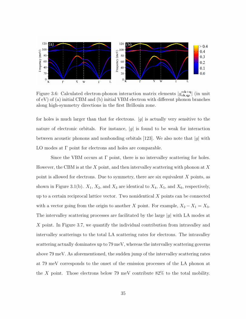
Figure 3.6: Calculated electron-phonon interaction matrix elements |gmk+qnk,qp | (in unit
of eV) of (a) initial CBM and (b) initial VBM electron with different phonon branchesalong high-symmetry directions in the first Brillouin zone.
for holes is much larger than that for electrons. |g| is actually very sensitive to the
nature of electronic orbitals. For instance, |g| is found to be weak for interaction
between acoustic phonons and nonbonding orbitals [123]. We also note that |g| with
LO modes at Γ point for electrons and holes are comparable.
Since the VBM occurs at Γ point, there is no intervalley scattering for holes.
However, the CBM is at theX point, and then intervalley scattering with phonon atX
point is allowed for electrons. Due to symmetry, there are six equivalent X points, as
shown in Figure 3.1(b). X1, X2, and X3 are identical to X4, X5, and X6, respectively,
up to a certain reciprocal lattice vector. Two nonidentical X points can be connected
with a vector going from the origin to another X point. For example, X2−X1 = X3.
The intervalley scattering processes are facilitated by the large |g| with LA modes at
X point. In Figure 3.7, we quantify the individual contribution from intravalley and
intervalley scatterings to the total LA scattering rates for electrons. The intravalley
scattering actually dominates up to 79 meV, whereas the intervalley scattering governs
above 79 meV. As aforementioned, the sudden jump of the intervalley scattering rates
at 79 meV corresponds to the onset of the emission processes of the LA phonon at
the X point. Those electrons below 79 meV contribute 82% to the total mobility.
35
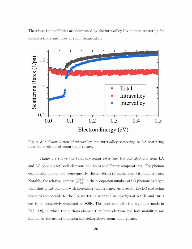
Therefore, the mobilities are dominated by the intravalley LA phonon scattering for
both electrons and holes at room temperature.
Figure 3.7: Contribution of intravalley and intervalley scattering to LA scatteringrates for electrons at room temperature.
Figure 3.8 shows the total scattering rates and the contributions from LA
and LO phonons for both electrons and holes at different temperatures. The phonon
occupation number and, consequently, the scattering rates, increase with temperature.
Notably, the relative increase nT2 (E)nT1 (E)
in the occupation number of LO phonons is larger
than that of LA phonons with increasing temperature. As a result, the LO scattering
becomes comparable to the LA scattering near the band edges at 600 K and turns
out to be completely dominant at 800K. This contrasts with the argument made in
Ref. [99], in which the authors claimed that both electron and hole mobilities are
limited by the acoustic phonon scattering above room temperature.
36
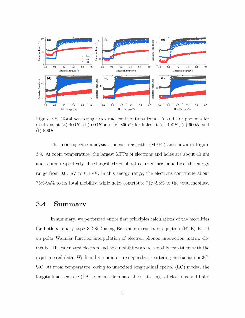
Figure 3.8: Total scattering rates and contributions from LA and LO phonons forelectrons at (a) 400K, (b) 600K and (c) 800K; for holes at (d) 400K, (e) 600K and(f) 800K
The mode-specific analysis of mean free paths (MFPs) are shown in Figure
3.9. At room temperature, the largest MFPs of electrons and holes are about 40 nm
and 15 nm, respectively. The largest MFPs of both carriers are found be of the energy
range from 0.07 eV to 0.1 eV. In this energy range, the electrons contribute about
75%-94% to its total mobility, while holes contribute 71%-93% to the total mobility.
3.4 Summary
In summary, we performed entire first principles calculations of the mobilities
for both n- and p-type 3C-SiC using Boltzmann transport equation (BTE) based
on polar Wannier function interpolation of electron-phonon interaction matrix ele-
ments. The calculated electron and hole mobilities are reasonably consistent with the
experimental data. We found a temperature dependent scattering mechanism in 3C-
SiC. At room temperature, owing to unexcited longitudinal optical (LO) modes, the
longitudinal acoustic (LA) phonons dominate the scatterings of electrons and holes
37

Figure 3.9: Mean free path of (a) electrons and (b) holes in 3C-SiC at 300K.
contributing to the mobilities. Specifically, the intravalley LA phonons dominate the
scatterings of electrons up to 79 meV, and the intervalley scattering becomes domi-
nant between 79 and 121 meV. The intervalley scattering is not present for holes. At
800K, LO-phonon interaction becomes the governing scattering mechanism for both
electrons and holes. The spin-orbit coupling almost has no influence on the calculated
mobilities, especially for the electrons. The largest carrier mean free path is about 40
nm for the electrons and 15 nm for the holes in 3C-SiC at room temperature.
38
Chapter 4
Anisotropic Thermoelectric
Performance of Magnesium
Antimonide
Till now, we have proved in Chapter 3 that our developed methods can suc-
cessfully reproduce the experimental measured carrier mobility for 3C-SiC without
any human-adjustable parameters. Combining with the phonon BTE, it is now pos-
sible to calculate the thermoelectric transport properties of thermoelectric materials.
In this chapter, we choose Mg3Sb2, which is rising star for moderate temperature
thermoelectric application. Another important reason for choosing Mg3Sb2 is that
its trigonal structure implies possible anisotropic thermoelectric transport properties,
which is hard to explore from the experimental point of view.
39
4.1 Introduction
Towards high zT, high crystal lattice symmetry is favored because high band
degeneracy and multiple pockets at the Fermi surface tend to yield high power fac-
tor (PF). [6, 124] In this vein, many state-of-the-art thermoelectric materials adopt
cubic structure: PbTe (Fm3m, space group No. 225) [6, 125], SnTe (Fm3m, space
group No. 225) [126, 127, 128], Mg2Si (Fm3m, space group No. 225) [129, 130],
CoSb3 (Im3, space group No. 204) [131, 132], half-Heusler alloys (F43m, space group
No. 216) [133, 134, 135], and Si-Ge alloys (F43m, space group No. 216) [136]. On
the other hand, some renowned thermoelectric materials possess lower crystal lattice
symmetry: Bi2Te3 (R3m, space group No. 166) [137, 138, 139], GeTe (R3m, space
group No. 166) [140], and SnSe (Pnma, space group No. 62) [52, 141, 142] and
owe their state-of-the-art thermoelectric performance largely to their intrinsically low
thermal conductivities. In the context of the classic phonon-glass and electron-crystal
paradigm [143, 144, 145], the cubic structured thermoelectric materials are in line of
electron-crystal, whereas lower lattice symmetry-structured materials emphasize the
aspect of phonon-glass to make good thermoelectrics.
Among low lattice symmetry thermoelectric materials, Zintl phase compounds
with a general formula AB2X2 and a space group P3m1 (space group No. 162) con-
stitute a notable family, in which A is the cation and BX together is the anion. Most
AB2X2 Zintl compounds are p-type semiconductors because of cationic vacancies
[146]. In light of the large phase space of AB2X2 to tune the electrical and thermal
transport properties, the ground-breaking discovery of Te-doped n-type Mg3Sb2 with
zT around 1.6 at 720 K has made Mg3Sb2-based compounds an active frontier of
current thermoelectric materials research [19]. The highest reported zT of n-type
Mg3Sb2 (Mn and Te co-doped Mg3Sb1.5Bi0.5) is 1.85 at 723 K [147]. Meanwhile, n-
40
type Mg3Bi2 with similar geometric structure as Mg3Sb2 is known to possess a peak
zT of around 0.9 at 350 K [148]. To date, the major challenge is the performance
imbalance between n-type and p-type Mg3Sb2. From a thermoelectric device perspec-
tive, it is desired to fabricate a device using n-type and p-type polycrystalline legs
made from the same parent compound and with comparable thermoelectric perfor-
mance. However, despite great efforts, the present highest zT of p-type Mg3Sb2-based
compounds is only about half of its n-type counterparts. The imposing need to de-
velop higher performance p-type Mg3Sb2-based compounds is the motivation of the
present work.
Toward higher performance p-type Mg3Sb2-based compounds, theoretical ef-
forts via orbital engineering [149] and experimental efforts via optimizing hole con-
centration as mentioned in Chapter 1 [15, 23, 150] have been exerted. Given the
relatively lower lattice symmetry (trigonal lattice), anisotropic electrical and thermal
transport properties including zT of Mg3Sb2-based compounds are expected. Crys-
tal structural anisotropy is not rare among thermoelectric materials, unnecessarily a
disadvantage in performance optimization. For instance, the out-of-plane electrical
resistivity of n-type is found to be three times higher than that of in-plane direction
with a wide temperature range [151]; for p-type SnSe, the in-plane zT is much higher
than that of out-of-plane direction [52, 141, 142]. However, experimentally exploring
the anisotropic transport properties of a structurally anisotropic thermoelectric ma-
terial is demanding; the characterization of single crystalline samples calls for large,
high-quality single crystal samples and transport measurements (aka the electrical
conductivity, Seebeck coefficient, and thermal conductivity) along major crystallo-
graphic axes; concerning the characterization of polycrystalline samples, especially
those prepared under uniaxial pressure, one must ensure all thermoelectric properties
are measured along the same direction to avoid the artifacts caused by the texture.
41

To date, there are only a few reports of the transport properties of single crys-
talline Mg3Sb2. The single crystals grown by Kim et al. were easily cleavable, and the
electrical resistivity measurements were performed in the ab-plane (hereafter called
in-plane) direction [12]. Another work on single crystalline Mg3Sb2−xBix by the same
group reported large anisotropy in the electrical resistivity, with the resistivity in
the out-of-plane (c-axis) direction orders of magnitude larger than the that along the
in-plane direction [13]. Xin et al. has found that for pristine Mg3Sb2, the in-plane
resistivity is two times larger than that of out-of-plane direction at 300 K [14]. Ow-
ing to the highly demanding requirements on the sample dimensions, the anisotropy
of thermal conductivity and Seebeck coefficient has not been reported experimen-
tally. To clarify the intrinsic thermoelectric properties, and thus the thermoelectric
potential of Mg3Sb2, it is highly desired to experimentally grow large, high quality-
single crystals and/or theoretically calculate the thermoelectric properties of pristine
Mg3Sb2.
As mentioned in Chapter 2, first principles calculations employing semiclassi-
cal transport equations (e.g. Boltzmann transport equations for charge carriers and
phonons) offer a great opportunity to fill out the knowledge gap of many anisotropic
thermoelectric materials that are hard to experimentally explore, including Mg3Sb2.
To this end, ab initio calculations of lattice thermal conductivity based on the three-
phonon process have matured nowadays [58, 152]. Several groups reported the nearly
isotropic lattice thermal conductivity of Mg3Sb2 along in-plane and out-of-plane di-
rections [17, 18]. Meanwhile, as the electrical transport properties are governed by
the electronic band structure and the specific carrier scattering mechanism, it is cru-
cial to deal with the scattering properly in the calculations. Previous calculations
of electrical transport properties on Mg3Sb2 employed constant relaxation time ap-
proximation (CRTA) [19, 146, 149, 153], in which relaxation time is an adjustable
42
single-value parameter. Apparently, it is hard for CRTA to capture the detailed scat-
tering mechanism of charge carriers. Given the complexity of both the structural
and electronic structure of Mg3Sb2, CRTA is oversimplified. On the other hand, it
is customarily accepted that electron-phonon interactions become the dominant scat-
tering mechanism at elevated temperatures. In Mg3Sb2, despite small contributions
from alloy scattering, the electron-acoustic phonon interactions dominate above 500
K [19, 20]. Pristine Mg3Sb2 is a semiconductor with a band gap around 0.4-0.6 eV
[17, 19, 154, 155] and a Debye temperature below 230 K [156]. Per the 10 kBT0 rule
[157], the optimal working temperature for Mg3Sb2 should be around 700-800 K. At
temperatures well above the Debye temperature, electron-phonon interaction is the
dominant scattering mechanism of charge carriers, making the results of theoretical
calculations based on electron-phonon interaction more reliable to be compared with
the experimental data.
Here, we use the state-of-the-art ab initio method to calculate the electron-
phonon interaction limited electrical transport properties via exact solutions of the
Boltzmann transport equation. When calculating the electron-phonon interaction
matrix elements, the contributions from all phonon branches (aka all modes in the
first Brillouin zone) are taken into account. It is of great interest to note the zT
of p-type Mg3Sb2 along its c-axis attained in this work is almost three times larger
than that along the a(b)-axis, with a zT around 1.5 at 750 K along the c-direction.
In n-type Mg3Sb2, both the electrical and thermal transport properties tend to be
isotropic, and our calculated zT value agrees well with experimental data of n-type
Mg3Sb2.
43
4.2 Computational Details
First principles calculations based on density functional theory (DFT) are car-
ried out to calculate electronic band structure with a 10×10×6 Monkhorst-Pack k grid
and cut-off energy of 50 Ry. Norm conserving fully relativistic pseudo-potentials with
local density approximation (LDA) [115] are employed. The phonon dispersion rela-
tion is calculated using density functional perturbation theory (DFPT) with a 5×5×3
q grid mesh. All these calculations are performed using Quantum Espresso software
package [114]. The relaxed geometrical structure of Mg3Sb2 is shown in Figure 4.1(a).
The calculated lattice constants are a=4.492 A and c=7.097 A, which agree well with
values measured experimentally (a=4.569 A and c=7.245 A) for Mg3Sb2 single crys-
tal [14]. The calculated phonon dispersion relation of Mg3Sb2 [Figure 4.1(d)] agrees
well with previous works [17, 18, 158, 159], especially for the low-frequency phonon
modes. In addition, our calculated Born effective charges are 3.10, 1.77 and -3.32 for
Mg1, Mg2 and Sb atoms are also in consistent with Ref[17, 18, 158, 159].
As aforementioned, the electrical transport properties in this work are based on
electron-phonon interaction. The correctness of electronic band structure is of great
importance. The calculated band gap of Mg3Sb2 using LDA is 0.051 eV as shown
in Figure 4.1(c). However, the band gaps obtained using Heyd-Scuseria-Ernzerhof
(HSE06) [160, 161, 162] and TB-mBJ potential [163] are 0.45 [17] and 0.6 eV [19],
respectively. Although these two methods could provide more accurate values of band
gap comparable to experimental measured values [154, 155], the band curvatures are
basically the same compared with LDA or PBE, and only the energy eigenvalues
are shifted [17]. The multivalley character of the conduction band is clear in our
calculated band structure [cf. Figure 4.1(c)]. The conduction band minimum (labeled
as CBM1) is located at point (0.0, 0.417,0.333) inside the first Brillouin zone as
44

Figure 4.1: (a) Geometric structure of Mg3Sb2. (b) First Brillouin zone and highsymmetry points. (c) Electronic band structure and (d) phonon dispersion relationalong high-symmetry directions in the first Brillouin zone.
pointed out in Zhang et al. [20] There are other two conduction band valleys: one is
at the K-point (labeled as CBM2) with an energy 0.067 eV above CBM1; the other
(CBM3) sits along the M-L direction, and its energy is 0.039 eV higher than CBM2.
The locations of these valleys and the energy difference among them are consistent
with previously reported values [20]. A single valley in the valence band is observed
at the point.
To calculate electron-phonon interaction limited electronic transport proper-
ties (aka electrical conductivity, Seebeck coefficient, and electrical thermal conductiv-
ity), Wannier function interpolation of electron-phonon coupling matrix is employed
45
as implemented in EPW package [85]. Both k (for electrons and holes) and q grids
(for phonons) are interpolated to 75×75×50 in Mg3Sb2. The electronic transport
properties are calculated with the methodology developed in Chapter 2, where the δ
functions involved are treated as Gaussian functions with physically adaptive broad-
ening parameters, making the calculation completely parameter free. To calculate,
the third-order anharmonic interatomic force constants are obtained using a 4×4×4
supercell with a force cutoff distance of 0.55 nm employed [58, 65]. The ShengBTE
package [58, 164] is used for solving the phonon BTE with 26×26×16 q sampling.
Owing to the relatively large atomic mass of Sb, spin-orbit coupling (SOC)
needs to be considered when calculating the band structure. It is observed in Mg3Sb2
that SOC effect has a great influence on the valence band, whereas its effect on the
conduction band is negligible as demonstrated in Chapter 3, which is consistent with
previous calculations [20]. Hence, SOC is included when calculating the electron-
phonon interaction matrix elements for valence band while excluded for conduction
band. Because electrons and holes are treated separately in this work, the band gap
has no influence on the calculated transport properties as indicated in Chapter 3
[165]. Given the band gap value of 0.45-0.6 eV [154, 155], the bipolar effect is less
severe than the case of other narrow band gap materials, e.g. Bi2Te3 [166] and not
taken into account in our calculations. As pointed out in the literature [20, 153] that
alloying does not substantially affect the electronic band structure of Mg3Sb2, herein
our calculations are conducted on the pristine Mg3Sb2.
4.3 Results and Discussions
The lattice thermal conductivity of materials depends largely on their bond-
ing properties (e.g. bond type, bond strength, and so on). The interlayer and in-
46
tralayer interactions in chemical bonding networks can be characterized by the ratio
of ρinter/ρintra, where ρinter and ρintra denote the electron density values at the bond
critical points of the interlayer and intralayer bonds, respectively [18]. In Mg3Sb2, the
value of ρinter/ρintra is close to unity [18], attesting similar interlayer and intralayer
interactions and thus nearly isotropic lattice thermal conductivity. Given a trigonal
crystal lattice such as Mg3Sb2, the physical properties, like effective mass and lattice
thermal conductivity in the ab-plane, should be isotropic because of symmetry. In
our calculations, it is found the lattice thermal conductivities are identical along a-
and b-axis. The lattice thermal conductivity along c axis is slightly larger than that
along a(b)-axis with the largest anisotropy (κcL/κaL) around 1.05, agreeing with the
analyses based on interlayer and intralayer interactions and Huang et al. and Tamaki
et al. [17, 21]. Hereafter, the degree of anisotropy is defined as the relevant physical
quantity along the c-axis divided by the counterpart along a(b)-axis.
In general, the temperature dependency of lattice thermal conductivity at-
tained in this work is in reasonable agreement with previous experimental efforts. It
is expected that the calculated lattice thermal conductivity [Figure 4.2(a)] is slightly
larger than the experimental results because our calculations do not take into ac-
count other phonon scattering mechanisms such as point-defects and grain boundary
scattering. Meanwhile, the calculated values obtained via similar methods by other
groups are smaller than experimental data [17, 18]. The discrepancy is likely because
of different functionals employed in computing the interatomic force constants. Thus,
LDA outperforms PBE in obtaining the lattice thermal conductivity for Mg3Sb2.
The anisotropy of the electrical conductivity is because of the difference of the
carrier velocity squared along different directions. Considering the carrier velocity
squared is inversely proportional to the effective mass, the effective mass difference
along different crystallographic axes could reflect the anisotropy of electrical conduc-
47
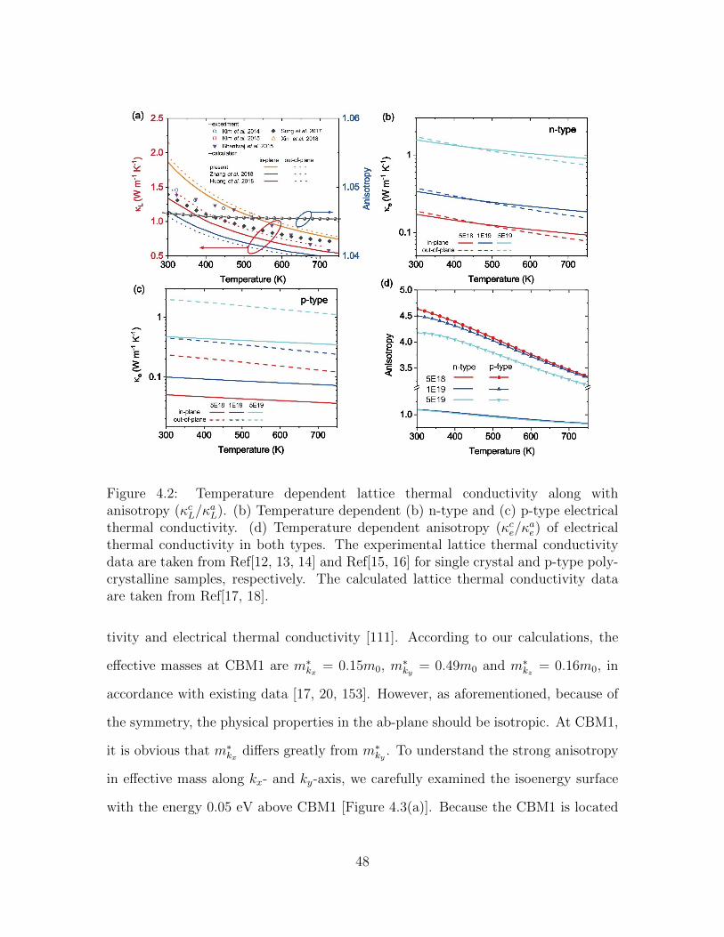
Figure 4.2: Temperature dependent lattice thermal conductivity along withanisotropy (κcL/κ
aL). (b) Temperature dependent (b) n-type and (c) p-type electrical
thermal conductivity. (d) Temperature dependent anisotropy (κce/κae) of electrical
thermal conductivity in both types. The experimental lattice thermal conductivitydata are taken from Ref[12, 13, 14] and Ref[15, 16] for single crystal and p-type poly-crystalline samples, respectively. The calculated lattice thermal conductivity dataare taken from Ref[17, 18].
tivity and electrical thermal conductivity [111]. According to our calculations, the
effective masses at CBM1 are m∗kx = 0.15m0, m∗ky = 0.49m0 and m∗kz = 0.16m0, in
accordance with existing data [17, 20, 153]. However, as aforementioned, because of
the symmetry, the physical properties in the ab-plane should be isotropic. At CBM1,
it is obvious that m∗kx differs greatly from m∗ky . To understand the strong anisotropy
in effective mass along kx- and ky-axis, we carefully examined the isoenergy surface
with the energy 0.05 eV above CBM1 [Figure 4.3(a)]. Because the CBM1 is located
48
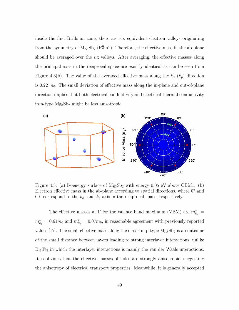
inside the first Brillouin zone, there are six equivalent electron valleys originating
from the symmetry of Mg3Sb2 (P3m1). Therefore, the effective mass in the ab-plane
should be averaged over the six valleys. After averaging, the effective masses along
the principal axes in the reciprocal space are exactly identical as can be seen from
Figure 4.3(b). The value of the averaged effective mass along the kx (ky) direction
is 0.22 m0. The small deviation of effective mass along the in-plane and out-of-plane
direction implies that both electrical conductivity and electrical thermal conductivity
in n-type Mg3Sb2 might be less anisotropic.
Figure 4.3: (a) Isoenergy surface of Mg3Sb2 with energy 0.05 eV above CBM1. (b)Electron effective mass in the ab-plane according to spatial directions, where 0◦ and60◦ correspond to the kx- and ky-axis in the reciprocal space, respectively.
The effective masses at Γ for the valence band maximum (VBM) are m∗kx =
m∗ky = 0.61m0 and m∗kz = 0.07m0, in reasonable agreement with previously reported
values [17]. The small effective mass along the c-axis in p-type Mg3Sb2 is an outcome
of the small distance between layers leading to strong interlayer interactions, unlike
Bi2Te3 in which the interlayer interactions is mainly the van der Waals interactions.
It is obvious that the effective masses of holes are strongly anisotropic, suggesting
the anisotropy of electrical transport properties. Meanwhile, it is generally accepted
49
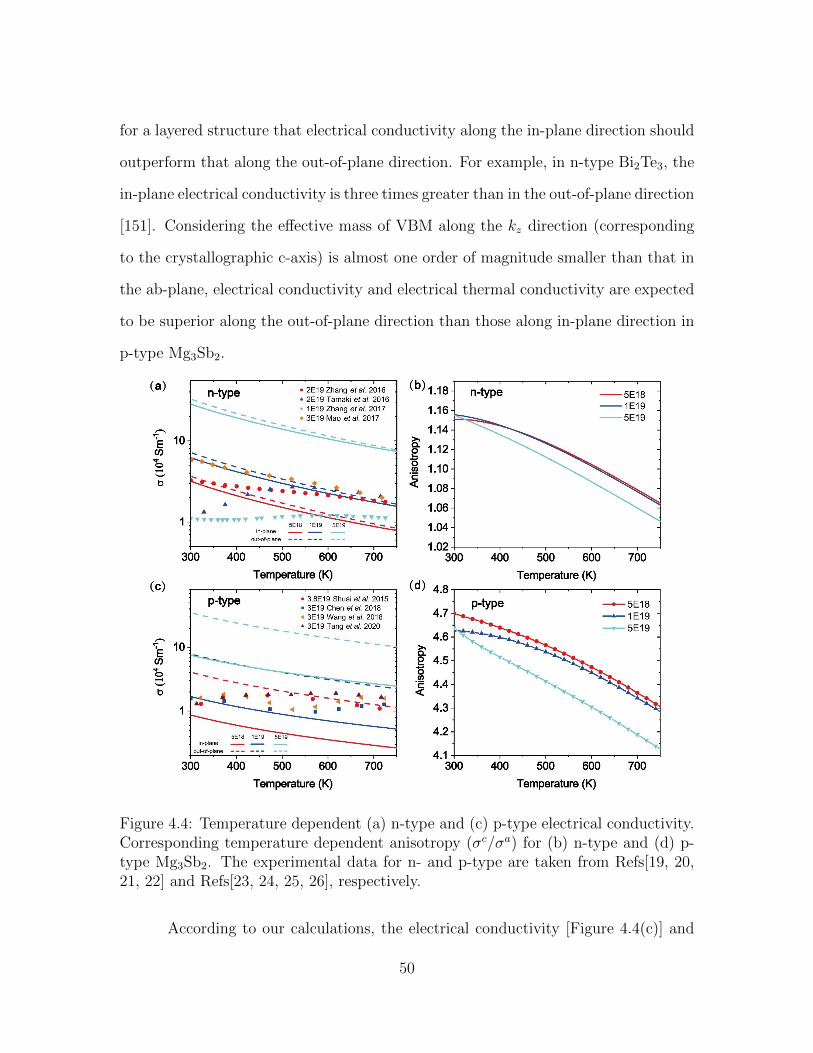
for a layered structure that electrical conductivity along the in-plane direction should
outperform that along the out-of-plane direction. For example, in n-type Bi2Te3, the
in-plane electrical conductivity is three times greater than in the out-of-plane direction
[151]. Considering the effective mass of VBM along the kz direction (corresponding
to the crystallographic c-axis) is almost one order of magnitude smaller than that in
the ab-plane, electrical conductivity and electrical thermal conductivity are expected
to be superior along the out-of-plane direction than those along in-plane direction in
p-type Mg3Sb2.
Figure 4.4: Temperature dependent (a) n-type and (c) p-type electrical conductivity.Corresponding temperature dependent anisotropy (σc/σa) for (b) n-type and (d) p-type Mg3Sb2. The experimental data for n- and p-type are taken from Refs[19, 20,21, 22] and Refs[23, 24, 25, 26], respectively.
According to our calculations, the electrical conductivity [Figure 4.4(c)] and
50

electrical thermal conductivity [Figure 4.2(c)] of p-type Mg3Sb2 along the c-axis are
indeed much larger than that in the ab-plane. At room temperature, the ratio of
anisotropy in both electrical conductivity and electrical thermal conductivity are close
in value; the largest ratio of anisotropy is around 4.6 [cf. Figures 4.2(d) and 4.4(d)].
The anisotropy value attained for p-type electrical conductivity at room temperature
is slightly larger than the experimental value reported by Xin et al. [14]. For the
n-type counterpart, both the attained electrical conductivity and electrical thermal
conductivity are nearly isotropic with the highest anisotropy around 1.15 at room
temperature [cf. Figures 4.2(d) and 4.4(b)], which is consistent with our analyses
based on effective mass.
Figure 4.5: Average carrier velocity and corresponding anisotropy (vc/va) for (a) n-type and (b) p-type Mg3Sb2.
To analyze the anisotropy quantitatively, we calculate the average carrier ve-
locity along different directions, which is obtained as:
vα(ε) =√∑
nk
|vαnk|2 δ (ε− εnk) /
∑nk
δ (ε− εnk), (4.1)
where εnk is the carrier energy at the nk state. It is clear from Figure 4.5(b) that
the average velocity along the c-direction is much larger than in the a(b)-direction
51
in p-type Mg3Sb2. The presence of a kink at around 0.35 eV indicates the second
valence band starts to contribute to electrical transport. The contribution from the
second valence band can also be seen from the hole scattering rates [Figure 4.6].
As can be seen from the band structure [Figure 4.1(c)], the effective mass along
the ab-plane of the second valence band does not vary much compared with VBM,
whereas it is larger in the c-direction, leading to a smaller vc/va at energies larger
than 0.35 eV. For n-type [Figure 4.5(a)], when the electron energy is below 0.2 eV,
the average velocities along a(b)- and c-axis are nearly identical, with an almost-
flat anisotropy within this energy range. Multiband conduction behavior is obvious
for n-type Mg3Sb2 from Figure 4.5(a) with more kinks as compared with p-type
Mg3Sb2, which are mainly because of the participation from sub-bands. Careful
inspection of the mode-specific scattering rates as a function of carrier energy (Figure
4.6) revealed that for both conduction types, carriers with low energy are scattered
dominantly by the two polar-LO-phonons [as demonstrated in Figure 4.1(d)], owing
to the large electron-phonon coupling constant of these two phonon branches because
of the electron-phonon interaction matrix elements of these two branches diverge as
1/|q| for |q| approaching zero [167]. As the energy of carriers increases, other phonon
modes start to contribute significantly to the total scattering.
Note that the carrier scattering by polar-LO phonons is sensitive to the dielec-
tric constant. The calculated dielectric constants are 13.5 and 16.2 along a(b)-axis
and c-axis, in good agreement with the literature data 13.8 and 16.4 along a(b)-axis
and c-axis, respectively [27]. In general, high carrier concentration tends to weaken
the screening effect, yielding longer carrier lifetime and higher carrier mobility [122].
In this work, the screening effect is not taken into account. Nonetheless, high carrier
concentration enhances electron-electron and electron-defect scattering, which de-
crease the carrier mobility and somewhat compensate for the effect of the weakened
52
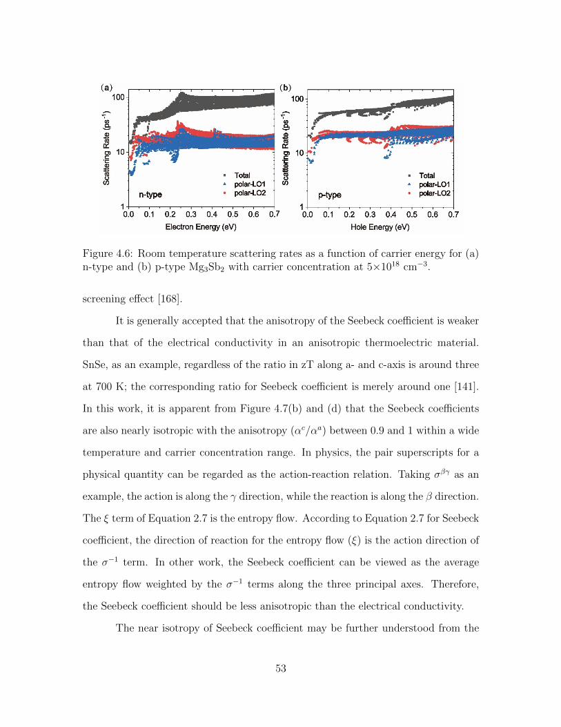
Figure 4.6: Room temperature scattering rates as a function of carrier energy for (a)n-type and (b) p-type Mg3Sb2 with carrier concentration at 5×1018 cm−3.
screening effect [168].
It is generally accepted that the anisotropy of the Seebeck coefficient is weaker
than that of the electrical conductivity in an anisotropic thermoelectric material.
SnSe, as an example, regardless of the ratio in zT along a- and c-axis is around three
at 700 K; the corresponding ratio for Seebeck coefficient is merely around one [141].
In this work, it is apparent from Figure 4.7(b) and (d) that the Seebeck coefficients
are also nearly isotropic with the anisotropy (αc/αa) between 0.9 and 1 within a wide
temperature and carrier concentration range. In physics, the pair superscripts for a
physical quantity can be regarded as the action-reaction relation. Taking σβγ as an
example, the action is along the γ direction, while the reaction is along the β direction.
The ξ term of Equation 2.7 is the entropy flow. According to Equation 2.7 for Seebeck
coefficient, the direction of reaction for the entropy flow (ξ) is the action direction of
the σ−1 term. In other work, the Seebeck coefficient can be viewed as the average
entropy flow weighted by the σ−1 terms along the three principal axes. Therefore,
the Seebeck coefficient should be less anisotropic than the electrical conductivity.
The near isotropy of Seebeck coefficient may be further understood from the
53
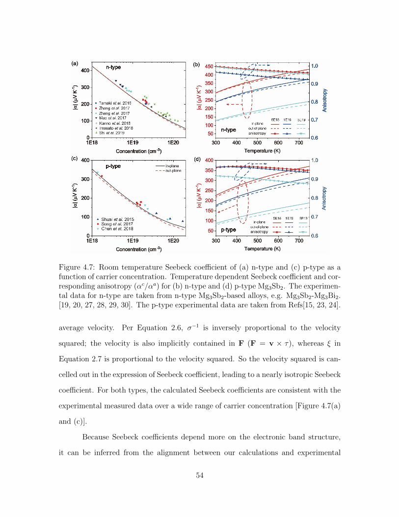
Figure 4.7: Room temperature Seebeck coefficient of (a) n-type and (c) p-type as afunction of carrier concentration. Temperature dependent Seebeck coefficient and cor-responding anisotropy (αc/αa) for (b) n-type and (d) p-type Mg3Sb2. The experimen-tal data for n-type are taken from n-type Mg3Sb2-based alloys, e.g. Mg3Sb2-Mg3Bi2.[19, 20, 27, 28, 29, 30]. The p-type experimental data are taken from Refs[15, 23, 24].
average velocity. Per Equation 2.6, σ−1 is inversely proportional to the velocity
squared; the velocity is also implicitly contained in F (F = v × τ), whereas ξ in
Equation 2.7 is proportional to the velocity squared. So the velocity squared is can-
celled out in the expression of Seebeck coefficient, leading to a nearly isotropic Seebeck
coefficient. For both types, the calculated Seebeck coefficients are consistent with the
experimental measured data over a wide range of carrier concentration [Figure 4.7(a)
and (c)].
Because Seebeck coefficients depend more on the electronic band structure,
it can be inferred from the alignment between our calculations and experimental
54
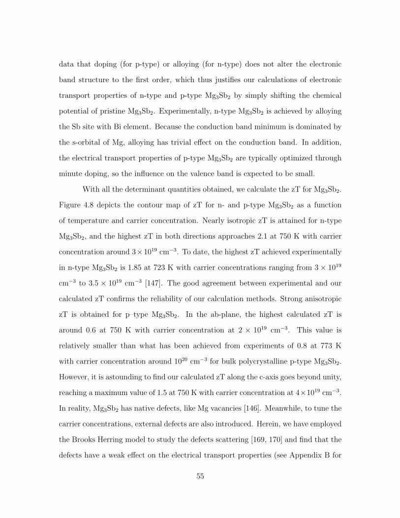
data that doping (for p-type) or alloying (for n-type) does not alter the electronic
band structure to the first order, which thus justifies our calculations of electronic
transport properties of n-type and p-type Mg3Sb2 by simply shifting the chemical
potential of pristine Mg3Sb2. Experimentally, n-type Mg3Sb2 is achieved by alloying
the Sb site with Bi element. Because the conduction band minimum is dominated by
the s-orbital of Mg, alloying has trivial effect on the conduction band. In addition,
the electrical transport properties of p-type Mg3Sb2 are typically optimized through
minute doping, so the influence on the valence band is expected to be small.
With all the determinant quantities obtained, we calculate the zT for Mg3Sb2.
Figure 4.8 depicts the contour map of zT for n- and p-type Mg3Sb2 as a function
of temperature and carrier concentration. Nearly isotropic zT is attained for n-type
Mg3Sb2, and the highest zT in both directions approaches 2.1 at 750 K with carrier
concentration around 3×1019 cm−3. To date, the highest zT achieved experimentally
in n-type Mg3Sb2 is 1.85 at 723 K with carrier concentrations ranging from 3× 10¹⁹
cm−3 to 3.5 × 1019 cm−3 [147]. The good agreement between experimental and our
calculated zT confirms the reliability of our calculation methods. Strong anisotropic
zT is obtained for p–type Mg3Sb2. In the ab-plane, the highest calculated zT is
around 0.6 at 750 K with carrier concentration at 2 × 1019 cm−3. This value is
relatively smaller than what has been achieved from experiments of 0.8 at 773 K
with carrier concentration around 1020 cm−3 for bulk polycrystalline p-type Mg3Sb2.
However, it is astounding to find our calculated zT along the c-axis goes beyond unity,
reaching a maximum value of 1.5 at 750 K with carrier concentration at 4×1019 cm−3.
In reality, Mg3Sb2 has native defects, like Mg vacancies [146]. Meanwhile, to tune the
carrier concentrations, external defects are also introduced. Herein, we have employed
the Brooks Herring model to study the defects scattering [169, 170] and find that the
defects have a weak effect on the electrical transport properties (see Appendix B for
55

details). Specifically, the zT along the c-axis of p-type Mg3Sb2 is still greater than
unity, with a maximum value of 1.42 at 750 K at a carrier concentration of 2× 10¹⁹
cm−3. This outcome is of great significance because it has been a long-going project to
discover the p-type Mg3Sb2 with zT above unity considering that both p- and n-type
legs are needed for power generation devices to maximize power output. It has been
reported that highly oriented, textured Bi2Te3 could have significantly enhanced zT
compared with a less-oriented sample [171, 172, 173]. Our finding could provide an
insightful guide for experimental work. For example, it might be possible to achieve
zT above unity for p-type Mg3Sb2 by properly oriented samples.
4.4 Summary
Anisotropic thermoelectric transport properties of pristine Mg3Sb2 are ex-
plored via parameter-free first principles calculations along with electron-phonon
interactions (phonon-phonon interaction) limited Boltzmann transport equation for
carriers (phonons) as implemented in Chapter 2. Nearly isotropic lattice thermal
conductivity and Seebeck coefficient are observed, both of which align with the ex-
perimental data. Electrical conductivity and carrier thermal conductivity for n-type
Mg3Sb2 are also nearly isotropic, originating from the similar effective masses along
the a(b)- and c-direction. In contrast, large anisotropy was found for p-types, with
the electrical conductivity and electrical thermal conductivity along the c-axis be-
ing four times of those in the ab-plane. The abnormal anisotropy is attributed to the
much lower effective mass along the c-direction than that along a(b)-direction. Unlike
Bi2Te3, Mg3Sb2 has strong inter-plane interactions, leading to a dispersive band along
the Γ-A direction (crystallographic c-axis). The calculated zT for n-type Mg3Sb2 was
2.1 at 750 K in accordance with experimental data. Strong anisotropy of zT is found
56
in p-type Mg3Sb2; the largest zT in ab-plane and c-direction are 0.6 and 1.5 at 750 K,
respectively. We also propose that, in practice, the performance of p-type zT might
be enhanced by properly texturing polycrystalline samples.
57
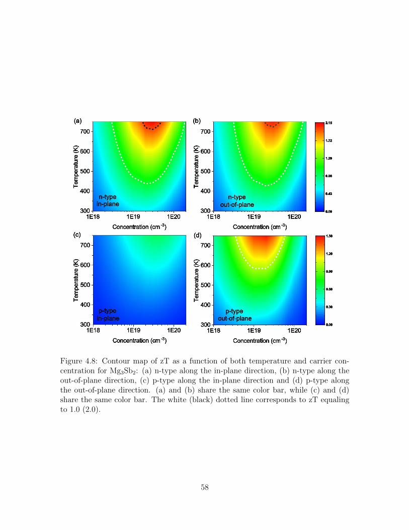
Figure 4.8: Contour map of zT as a function of both temperature and carrier con-centration for Mg3Sb2: (a) n-type along the in-plane direction, (b) n-type along theout-of-plane direction, (c) p-type along the in-plane direction and (d) p-type alongthe out-of-plane direction. (a) and (b) share the same color bar, while (c) and (d)share the same color bar. The white (black) dotted line corresponds to zT equalingto 1.0 (2.0).
58

Chapter 5
Strain Effects on the
Thermoelectric Performance of
Two-dimensional alpha-Tellurium
After the discovery of graphene in the year 2004, physical properties of two
dimensional materials have attracted tremendous attention. The thermoelectric per-
formance of two dimensional materials is still an open question. Two dimensional
transition metal dichalcogenides are reported to have large power factors; however,
they are accompanied by large lattice thermal conductivity. Recently, it has been
found that two dimensional alpha-tellurium exhibits low lattice thermal conductiv-
ity, which is a prefactor for excellent thermoelectric performance. Nevertheless, its
thermoelectric performance is less studied. In this chapter, we calculated the ther-
moelectric transport properties of two dimensional alpha-tellurium without external
strain and with tensile strain up to 4%, with the expectation to show our developed
methods are able to handle the cases with reduced dimensionality.
59
5.1 Introduction
Two-dimensional (2D) materials have attracted tremendous interests from the
point of view of reduced dimensionality as they can be cleaved or made nanosized.
In the field of thermoelectric material research, 2D materials such as transition metal
dichalcogenides (TMDs) [174, 175] have demonstrated their promise by possessing
a large power factor (PF) comparable with the state-of-the-art bulk thermoelectric
materials. On the other hand, TMDs often have thermal conductivities too high for
good thermoelectrics. In parallel with the experimental study, theoretical calculations
typically involved with simplifications on an electronic band structure and a scattering
rate have been carried out to explore the thermoelectric promise of many 2D materials
including MX2 (M = Mo, W; X = S, Se), [176, 177, 178] MCO2 (M = Ti, Zr, Hf)
[179], TiS2 [180], ZrS2 [181], TiS3 [182], black phosphorene [183], PdXY (X, Y = S,
Se, Te) [184, 185], and Bi2Te2X (X = S, Se, Te) [186], to name a few. The results
of these calculations do not yield zT values above unity due to a low power factor
and/or high thermal conductivity. Recently, promisingly high zT values are predicted
in emerging 2D materials, such as PbI2 [187], KAgSe [188] and pentasilicene [189].
Nonetheless, the phenomenological models with simplifications generally lack enough
predictive power. Hence, there is a demanding need for first principles (parameter-
free) calculations of the performance of thermoelectric materials using the methods
developed in Chapter 2.
From the computational perspective, the materials to be modeled would be
structurally simple enough so the results are reliable yet thermoelectrically good
enough. Therefore, the results are of immediate practical implication. Elemental
Te is such a material. Recently, Lin et al. [190] reported polycrystalline bulk Te as a
good thermoelectric material with zT up to 1.0 at 600 K. zT = 1.0 is regarded as the
60
benchmark for practical thermoelectric materials. This discovery is ground breaking
in that most known good thermoelectric materials are multinary semiconductors or
semimetals, whereas Te is elemental. On the other hand, the experimental results
of Te are derived from polycrystalline samples, which does not fully reflect the ther-
moelectric potential of Te, given its anisotropic crystal structure. Hence, inspired by
the reduced dimensionality approach mentioned above and in the light of the lay-
ered crystal structure of Te, the intrinsic thermoelectric performance of monolayer Te
needs to be studied.
To this end, Zhu et al. [191] predicted that monolayer Te could possess two
semiconductor phases, named α-Te and β-Te using density functional theory (DFT)
calculations. The α-Te phase is stable, whereas β-Te is metastable. [191] The authors
also pointed out that monolayer α-Te could be readily obtained via a thickness-
dependent structural phase transition along the [001] direction of the trigonal bulk
Te, whereas the β-Te phase could be derived by the structural relaxation when the
bulk helical chain structure is truncated along the equivalent [010] or [100] direction.
So far, only the β-Te phase has been experimentally obtained using molecular beam
epitaxy growth on a highly oriented pyrolytic graphite (HOPG) substrate [191, 192]
and a graphene/6H-SiC substrate [193]. The interactions from the substrate during
Te growth prevent β-Te from transforming into a more stable α phase. Nonetheless,
when grown on a substrate that is more chemically bounded (yet not too strong) than
HOPG and graphene/6H-SiC substrate, α-Te is expected. [191]
Regarding the thermoelectric performance of monolayer Te, previous studies
showed that κL of α- and β-Te are lower than 10 Wm−1K−1 above room tempera-
ture, [194, 195, 196] much smaller than that of monolayer TMDs. [197, 198] Nonethe-
less, the studies of full thermoelectric transport properties are scarce. The electrical
transport properties in previous studies are estimated based on a roughly constant
61
relaxation time, [195, 196] which in real life depends on carrier modes, carrier con-
centrations, and temperatures. Therefore, more accurate study is highly desired.
To accurately calculate the electrical transport properties, first principles calcula-
tions have not been made possible until recently by solving the Boltzmann transport
equations (BTE) with scattering limited by the electron-phonon interactions obtained
from DFT and density functional perturbation theory (DFPT). [77, 81, 199, 200, 201]
Electron phonon interactions are typically the dominant mechanism at an elevated
temperature, where the zT value peaks. In this work, we calculate full thermoelectric
transport properties along with zT of the monolayer α-Te from first principles and
parameter-free BTE. Considering the fact that the monolayer Te is grown on a sub-
strate, mismatch in the lattice constants could result in strain, either compressive or
tensile; the strain effect is studied.
5.2 Computational Details
The DFT and DFPT calculations were carried out in the Quantum Espresso
package [114] using full relativistic norm-conserving pseudopotentials with local den-
sity approximation (LDA) exchange-correlation functional. [115] Figure 5.1 shows the
crystal structure of monolayer α-Te in the real space, which adopts a trigonal P3m1
(No. 164) space group. The relaxed lattice constant is a = 4.14 A, in agreement with
the literature data. [191, 195] In a side view, there are three Te atomic planes, with
a distance between the upper and lower atomic planes of d = 3.60 A. The crystal
structure is not mirror symmetrized with respect to the middle atomic plane. The
vacuum space perpendicular to the atomic plane was fixed to be 20 A to eliminate
the interactions between layers. For the properties normalized by volume, an effec-
tive thickness of 7.72 A was adopted, also known as the distance between surface Te
62
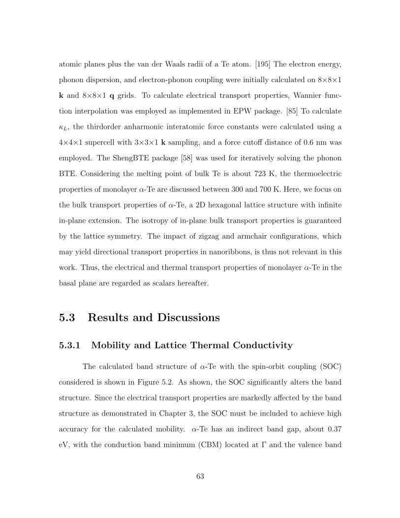
atomic planes plus the van der Waals radii of a Te atom. [195] The electron energy,
phonon dispersion, and electron-phonon coupling were initially calculated on 8×8×1
k and 8×8×1 q grids. To calculate electrical transport properties, Wannier func-
tion interpolation was employed as implemented in EPW package. [85] To calculate
κL, the thirdorder anharmonic interatomic force constants were calculated using a
4×4×1 supercell with 3×3×1 k sampling, and a force cutoff distance of 0.6 nm was
employed. The ShengBTE package [58] was used for iteratively solving the phonon
BTE. Considering the melting point of bulk Te is about 723 K, the thermoelectric
properties of monolayer α-Te are discussed between 300 and 700 K. Here, we focus on
the bulk transport properties of α-Te, a 2D hexagonal lattice structure with infinite
in-plane extension. The isotropy of in-plane bulk transport properties is guaranteed
by the lattice symmetry. The impact of zigzag and armchair configurations, which
may yield directional transport properties in nanoribbons, is thus not relevant in this
work. Thus, the electrical and thermal transport properties of monolayer α-Te in the
basal plane are regarded as scalars hereafter.
5.3 Results and Discussions
5.3.1 Mobility and Lattice Thermal Conductivity
The calculated band structure of α-Te with the spin-orbit coupling (SOC)
considered is shown in Figure 5.2. As shown, the SOC significantly alters the band
structure. Since the electrical transport properties are markedly affected by the band
structure as demonstrated in Chapter 3, the SOC must be included to achieve high
accuracy for the calculated mobility. α-Te has an indirect band gap, about 0.37
eV, with the conduction band minimum (CBM) located at Γ and the valence band
63
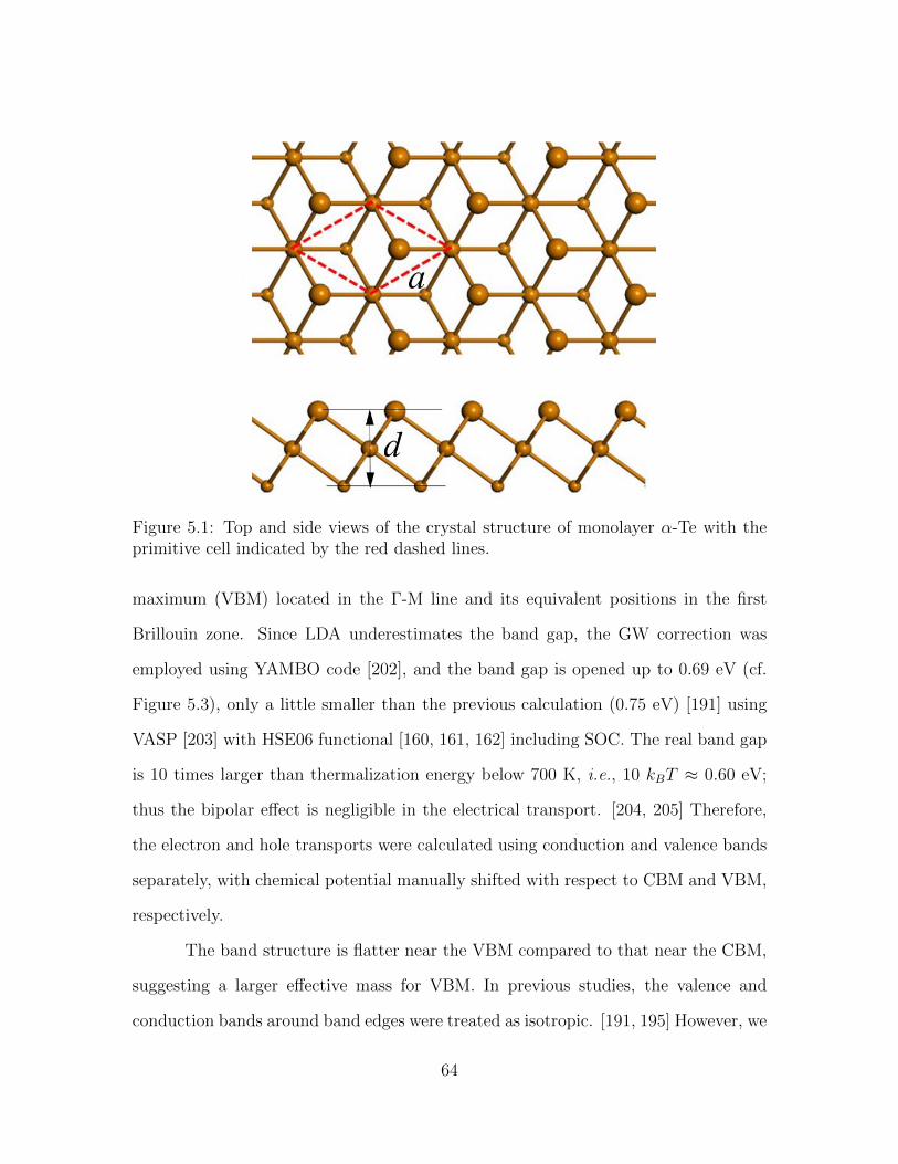
Figure 5.1: Top and side views of the crystal structure of monolayer α-Te with theprimitive cell indicated by the red dashed lines.
maximum (VBM) located in the Γ-M line and its equivalent positions in the first
Brillouin zone. Since LDA underestimates the band gap, the GW correction was
employed using YAMBO code [202], and the band gap is opened up to 0.69 eV (cf.
Figure 5.3), only a little smaller than the previous calculation (0.75 eV) [191] using
VASP [203] with HSE06 functional [160, 161, 162] including SOC. The real band gap
is 10 times larger than thermalization energy below 700 K, i.e., 10 kBT ≈ 0.60 eV;
thus the bipolar effect is negligible in the electrical transport. [204, 205] Therefore,
the electron and hole transports were calculated using conduction and valence bands
separately, with chemical potential manually shifted with respect to CBM and VBM,
respectively.
The band structure is flatter near the VBM compared to that near the CBM,
suggesting a larger effective mass for VBM. In previous studies, the valence and
conduction bands around band edges were treated as isotropic. [191, 195] However, we
64
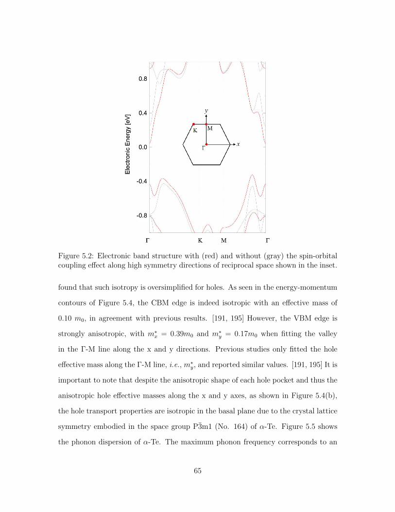
Figure 5.2: Electronic band structure with (red) and without (gray) the spin-orbitalcoupling effect along high symmetry directions of reciprocal space shown in the inset.
found that such isotropy is oversimplified for holes. As seen in the energy-momentum
contours of Figure 5.4, the CBM edge is indeed isotropic with an effective mass of
0.10 m0, in agreement with previous results. [191, 195] However, the VBM edge is
strongly anisotropic, with m∗x = 0.39m0 and m∗y = 0.17m0 when fitting the valley
in the Γ-M line along the x and y directions. Previous studies only fitted the hole
effective mass along the Γ-M line, i.e., m∗y, and reported similar values. [191, 195] It is
important to note that despite the anisotropic shape of each hole pocket and thus the
anisotropic hole effective masses along the x and y axes, as shown in Figure 5.4(b),
the hole transport properties are isotropic in the basal plane due to the crystal lattice
symmetry embodied in the space group P3m1 (No. 164) of α-Te. Figure 5.5 shows
the phonon dispersion of α-Te. The maximum phonon frequency corresponds to an
65
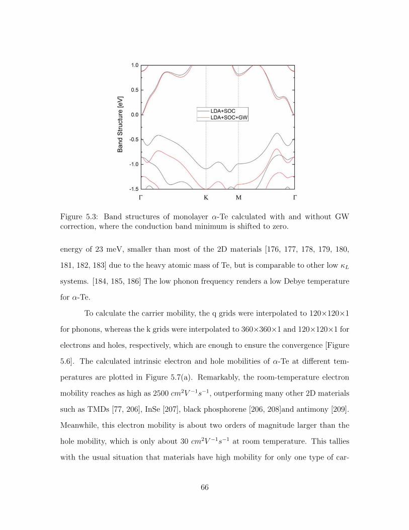
Figure 5.3: Band structures of monolayer α-Te calculated with and without GWcorrection, where the conduction band minimum is shifted to zero.
energy of 23 meV, smaller than most of the 2D materials [176, 177, 178, 179, 180,
181, 182, 183] due to the heavy atomic mass of Te, but is comparable to other low κL
systems. [184, 185, 186] The low phonon frequency renders a low Debye temperature
for α-Te.
To calculate the carrier mobility, the q grids were interpolated to 120×120×1
for phonons, whereas the k grids were interpolated to 360×360×1 and 120×120×1 for
electrons and holes, respectively, which are enough to ensure the convergence [Figure
5.6]. The calculated intrinsic electron and hole mobilities of α-Te at different tem-
peratures are plotted in Figure 5.7(a). Remarkably, the room-temperature electron
mobility reaches as high as 2500 cm2V −1s−1, outperforming many other 2D materials
such as TMDs [77, 206], InSe [207], black phosphorene [206, 208]and antimony [209].
Meanwhile, this electron mobility is about two orders of magnitude larger than the
hole mobility, which is only about 30 cm2V −1s−1 at room temperature. This tallies
with the usual situation that materials have high mobility for only one type of car-
66
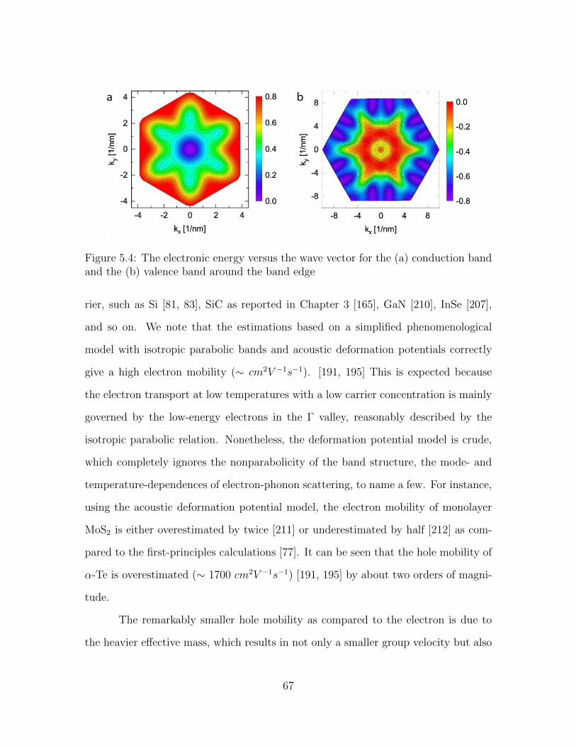
Figure 5.4: The electronic energy versus the wave vector for the (a) conduction bandand the (b) valence band around the band edge
rier, such as Si [81, 83], SiC as reported in Chapter 3 [165], GaN [210], InSe [207],
and so on. We note that the estimations based on a simplified phenomenological
model with isotropic parabolic bands and acoustic deformation potentials correctly
give a high electron mobility (∼ cm2V −1s−1). [191, 195] This is expected because
the electron transport at low temperatures with a low carrier concentration is mainly
governed by the low-energy electrons in the Γ valley, reasonably described by the
isotropic parabolic relation. Nonetheless, the deformation potential model is crude,
which completely ignores the nonparabolicity of the band structure, the mode- and
temperature-dependences of electron-phonon scattering, to name a few. For instance,
using the acoustic deformation potential model, the electron mobility of monolayer
MoS2 is either overestimated by twice [211] or underestimated by half [212] as com-
pared to the first-principles calculations [77]. It can be seen that the hole mobility of
α-Te is overestimated (∼ 1700 cm2V −1s−1) [191, 195] by about two orders of magni-
tude.
The remarkably smaller hole mobility as compared to the electron is due to
the heavier effective mass, which results in not only a smaller group velocity but also
67
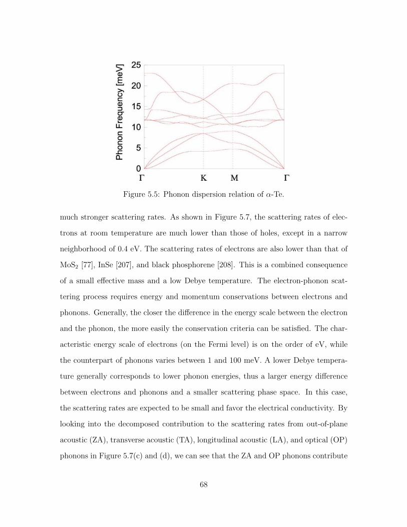
Figure 5.5: Phonon dispersion relation of α-Te.
much stronger scattering rates. As shown in Figure 5.7, the scattering rates of elec-
trons at room temperature are much lower than those of holes, except in a narrow
neighborhood of 0.4 eV. The scattering rates of electrons are also lower than that of
MoS2 [77], InSe [207], and black phosphorene [208]. This is a combined consequence
of a small effective mass and a low Debye temperature. The electron-phonon scat-
tering process requires energy and momentum conservations between electrons and
phonons. Generally, the closer the difference in the energy scale between the electron
and the phonon, the more easily the conservation criteria can be satisfied. The char-
acteristic energy scale of electrons (on the Fermi level) is on the order of eV, while
the counterpart of phonons varies between 1 and 100 meV. A lower Debye tempera-
ture generally corresponds to lower phonon energies, thus a larger energy difference
between electrons and phonons and a smaller scattering phase space. In this case,
the scattering rates are expected to be small and favor the electrical conductivity. By
looking into the decomposed contribution to the scattering rates from out-of-plane
acoustic (ZA), transverse acoustic (TA), longitudinal acoustic (LA), and optical (OP)
phonons in Figure 5.7(c) and (d), we can see that the ZA and OP phonons contribute
68
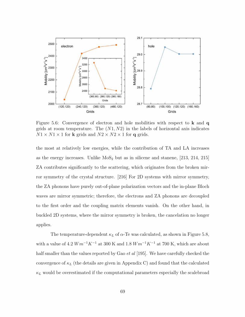
Figure 5.6: Convergence of electron and hole mobilities with respect to k and qgrids at room temperature. The (N1, N2) in the labels of horizontal axis indicatesN1×N1× 1 for k grids and N2×N2× 1 for q grids.
the most at relatively low energies, while the contribution of TA and LA increases
as the energy increases. Unlike MoS2 but as in silicene and stanene, [213, 214, 215]
ZA contributes significantly to the scattering, which originates from the broken mir-
ror symmetry of the crystal structure. [216] For 2D systems with mirror symmetry,
the ZA phonons have purely out-of-plane polarization vectors and the in-plane Bloch
waves are mirror symmetric; therefore, the electrons and ZA phonons are decoupled
to the first order and the coupling matrix elements vanish. On the other hand, in
buckled 2D systems, where the mirror symmetry is broken, the cancelation no longer
applies.
The temperature-dependent κL of α-Te was calculated, as shown in Figure 5.8,
with a value of 4.2 Wm−1K−1 at 300 K and 1.8 Wm−1K−1 at 700 K, which are about
half smaller than the values reported by Gao et al [195]. We have carefully checked the
convergence of κL (the details are given in Appendix C) and found that the calculated
κL would be overestimated if the computational parameters especially the scalebroad
69
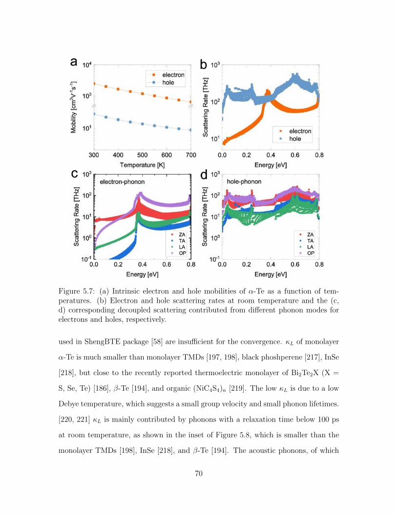
Figure 5.7: (a) Intrinsic electron and hole mobilities of α-Te as a function of tem-peratures. (b) Electron and hole scattering rates at room temperature and the (c,d) corresponding decoupled scattering contributed from different phonon modes forelectrons and holes, respectively.
used in ShengBTE package [58] are insufficient for the convergence. κL of monolayer
α-Te is much smaller than monolayer TMDs [197, 198], black phoshperene [217], InSe
[218], but close to the recently reported thermoelectric monolayer of Bi2Te2X (X =
S, Se, Te) [186], β-Te [194], and organic (NiC4S4)n [219]. The low κL is due to a low
Debye temperature, which suggests a small group velocity and small phonon lifetimes.
[220, 221] κL is mainly contributed by phonons with a relaxation time below 100 ps
at room temperature, as shown in the inset of Figure 5.8, which is smaller than the
monolayer TMDs [198], InSe [218], and β-Te [194]. The acoustic phonons, of which
70
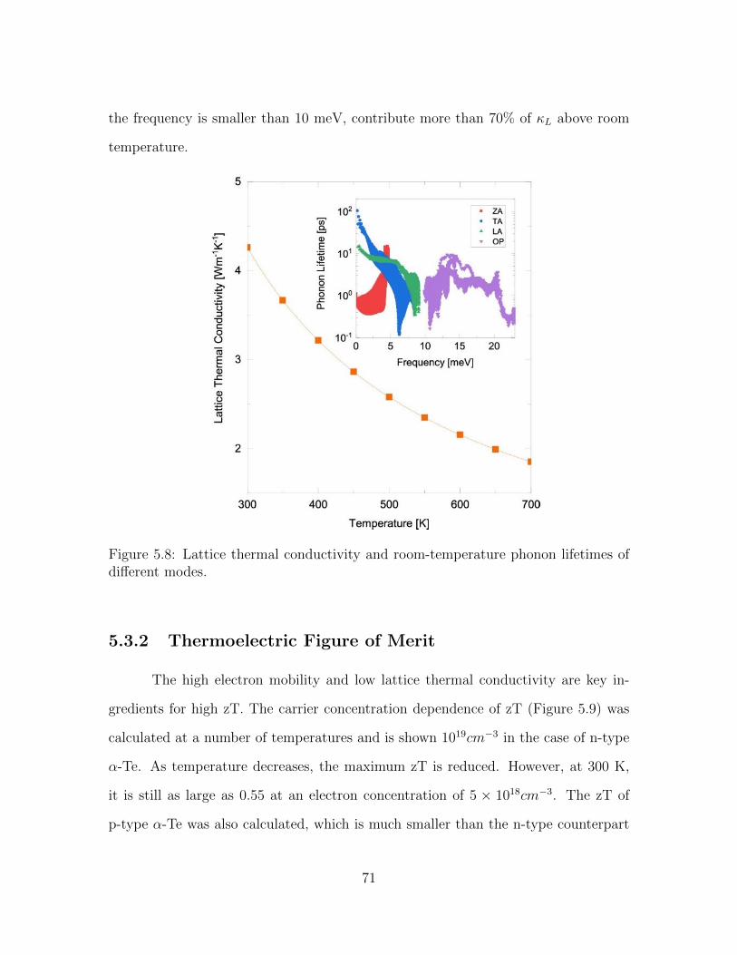
the frequency is smaller than 10 meV, contribute more than 70% of κL above room
temperature.
Figure 5.8: Lattice thermal conductivity and room-temperature phonon lifetimes ofdifferent modes.
5.3.2 Thermoelectric Figure of Merit
The high electron mobility and low lattice thermal conductivity are key in-
gredients for high zT. The carrier concentration dependence of zT (Figure 5.9) was
calculated at a number of temperatures and is shown 1019cm−3 in the case of n-type
α-Te. As temperature decreases, the maximum zT is reduced. However, at 300 K,
it is still as large as 0.55 at an electron concentration of 5 × 1018cm−3. The zT of
p-type α-Te was also calculated, which is much smaller than the n-type counterpart
71
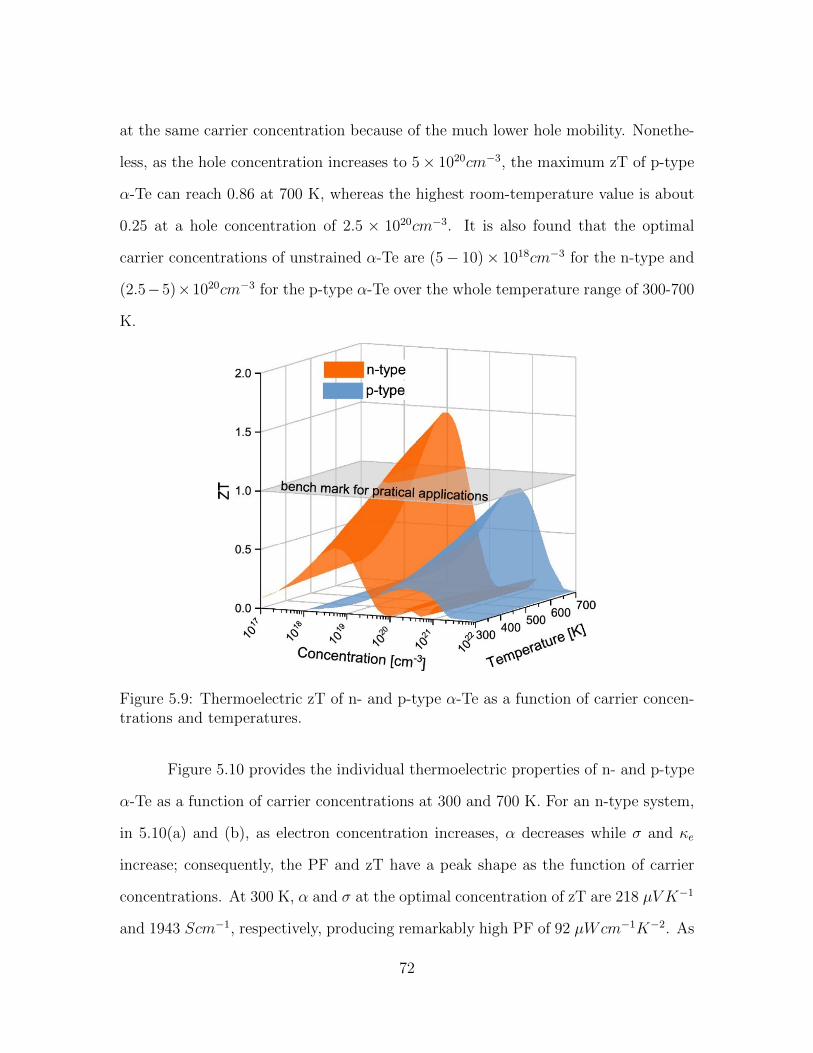
at the same carrier concentration because of the much lower hole mobility. Nonethe-
less, as the hole concentration increases to 5× 1020cm−3, the maximum zT of p-type
α-Te can reach 0.86 at 700 K, whereas the highest room-temperature value is about
0.25 at a hole concentration of 2.5 × 1020cm−3. It is also found that the optimal
carrier concentrations of unstrained α-Te are (5− 10)× 1018cm−3 for the n-type and
(2.5−5)×1020cm−3 for the p-type α-Te over the whole temperature range of 300-700
K.
Figure 5.9: Thermoelectric zT of n- and p-type α-Te as a function of carrier concen-trations and temperatures.
Figure 5.10 provides the individual thermoelectric properties of n- and p-type
α-Te as a function of carrier concentrations at 300 and 700 K. For an n-type system,
in 5.10(a) and (b), as electron concentration increases, α decreases while σ and κe
increase; consequently, the PF and zT have a peak shape as the function of carrier
concentrations. At 300 K, α and σ at the optimal concentration of zT are 218 µV K−1
and 1943 Scm−1, respectively, producing remarkably high PF of 92 µWcm−1K−2. As
72
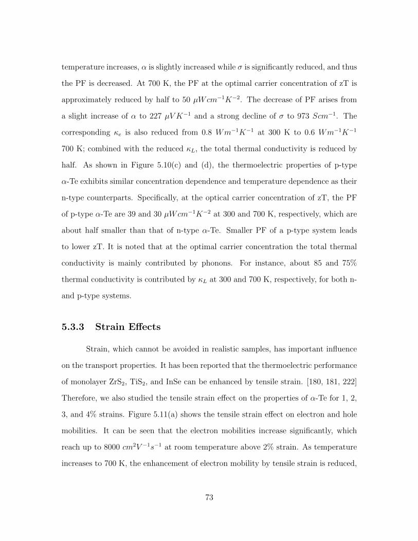
temperature increases, α is slightly increased while σ is significantly reduced, and thus
the PF is decreased. At 700 K, the PF at the optimal carrier concentration of zT is
approximately reduced by half to 50 µWcm−1K−2. The decrease of PF arises from
a slight increase of α to 227 µV K−1 and a strong decline of σ to 973 Scm−1. The
corresponding κe is also reduced from 0.8 Wm−1K−1 at 300 K to 0.6 Wm−1K−1
700 K; combined with the reduced κL, the total thermal conductivity is reduced by
half. As shown in Figure 5.10(c) and (d), the thermoelectric properties of p-type
α-Te exhibits similar concentration dependence and temperature dependence as their
n-type counterparts. Specifically, at the optical carrier concentration of zT, the PF
of p-type α-Te are 39 and 30 µWcm−1K−2 at 300 and 700 K, respectively, which are
about half smaller than that of n-type α-Te. Smaller PF of a p-type system leads
to lower zT. It is noted that at the optimal carrier concentration the total thermal
conductivity is mainly contributed by phonons. For instance, about 85 and 75%
thermal conductivity is contributed by κL at 300 and 700 K, respectively, for both n-
and p-type systems.
5.3.3 Strain Effects
Strain, which cannot be avoided in realistic samples, has important influence
on the transport properties. It has been reported that the thermoelectric performance
of monolayer ZrS2, TiS2, and InSe can be enhanced by tensile strain. [180, 181, 222]
Therefore, we also studied the tensile strain effect on the properties of α-Te for 1, 2,
3, and 4% strains. Figure 5.11(a) shows the tensile strain effect on electron and hole
mobilities. It can be seen that the electron mobilities increase significantly, which
reach up to 8000 cm2V −1s−1 at room temperature above 2% strain. As temperature
increases to 700 K, the enhancement of electron mobility by tensile strain is reduced,
73
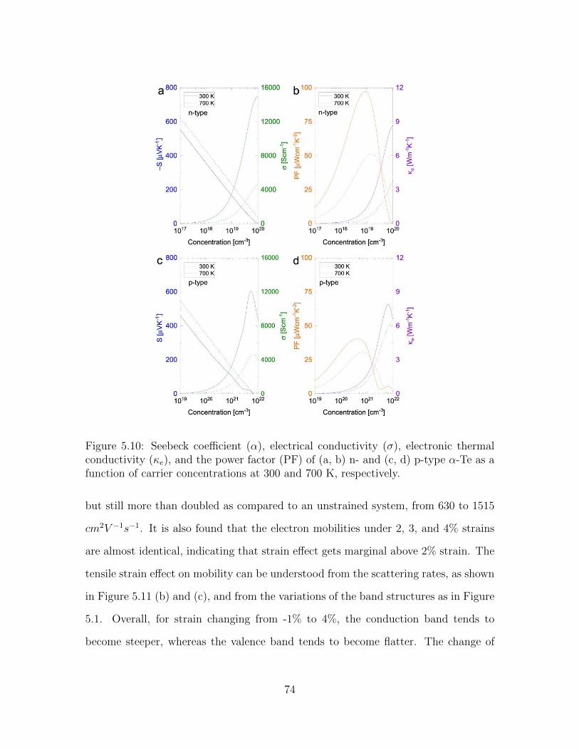
Figure 5.10: Seebeck coefficient (α), electrical conductivity (σ), electronic thermalconductivity (κe), and the power factor (PF) of (a, b) n- and (c, d) p-type α-Te as afunction of carrier concentrations at 300 and 700 K, respectively.
but still more than doubled as compared to an unstrained system, from 630 to 1515
cm2V −1s−1. It is also found that the electron mobilities under 2, 3, and 4% strains
are almost identical, indicating that strain effect gets marginal above 2% strain. The
tensile strain effect on mobility can be understood from the scattering rates, as shown
in Figure 5.11 (b) and (c), and from the variations of the band structures as in Figure
5.1. Overall, for strain changing from -1% to 4%, the conduction band tends to
become steeper, whereas the valence band tends to become flatter. The change of
74
band structure around CMB and VBM is not significant. To better characterize the
small changes of effective mass under stains, we derived the fitting from the constant
energy contours as in Figure 5.13. The fitted effective masses are listed in Table 5.1.
The valley around CBM is located at Gamma point and is isotropic, as shown in
Figure 5.13(a). When the strain varies from -1% to 4%, the electron effective mass is
slightly reduced. The valley around VBM is not located at Γ point, and thus there
are six equivalent valleys originating from the lattice crystal symmetry, as shown in
Figure 5.13(a). As the strain varies from -1% to 4%, the hole effective mass along
the y-direction is clearly increased, whereas the hole effective mass in the x-direction
does not vary monotonically due to the strong nonparabolicity. However, since the
change of the constant energy contour in the y-direction is larger than that in the
x-direction, as shown in 5.13(b), the enlarged area of constant energy contour implies
the equivalent increase for hole effective mass.
For an unstrained system, the ZA phonons dominate the scattering of elec-
trons at low energies as compared to other phonon modes, partially because of the
divergent thermal population of the quadratic ZA phonons. [216] Upon strain, the
ZA phonons get stiffened, and the dispersion changes from quadratic to linear as
in Figure 5.14. Consequently, the thermal population of the quadratic ZA phonons
is significantly reduced. Therefore, the scattering rates by ZA phonons decrease by
more than one order of magnitude at 2, 3, and 4% strains. For a given electron state,
smaller effective mass means fewer electron states available for phonon scattering in
the momentum space. The small scattering phase space corresponds to a small scat-
tering rate. The scattering rates by TA, LA, and OP phonons are almost unchanged,
implying the weak effect from the change of electron effective mass. Therefore, the
significant enhancement of electron mobility stems from the great decrease of electron-
ZA phonons scattering. As for holes, we found that the tensile strain also reduces the
75
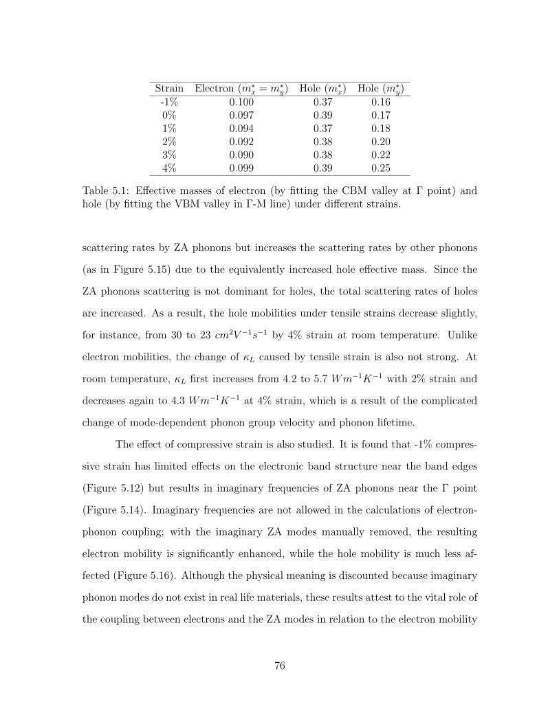
Strain Electron (m∗x = m∗y) Hole (m∗x) Hole (m∗y)
-1% 0.100 0.37 0.160% 0.097 0.39 0.171% 0.094 0.37 0.182% 0.092 0.38 0.203% 0.090 0.38 0.224% 0.099 0.39 0.25
Table 5.1: Effective masses of electron (by fitting the CBM valley at Γ point) andhole (by fitting the VBM valley in Γ-M line) under different strains.
scattering rates by ZA phonons but increases the scattering rates by other phonons
(as in Figure 5.15) due to the equivalently increased hole effective mass. Since the
ZA phonons scattering is not dominant for holes, the total scattering rates of holes
are increased. As a result, the hole mobilities under tensile strains decrease slightly,
for instance, from 30 to 23 cm2V −1s−1 by 4% strain at room temperature. Unlike
electron mobilities, the change of κL caused by tensile strain is also not strong. At
room temperature, κL first increases from 4.2 to 5.7 Wm−1K−1 with 2% strain and
decreases again to 4.3 Wm−1K−1 at 4% strain, which is a result of the complicated
change of mode-dependent phonon group velocity and phonon lifetime.
The effect of compressive strain is also studied. It is found that -1% compres-
sive strain has limited effects on the electronic band structure near the band edges
(Figure 5.12) but results in imaginary frequencies of ZA phonons near the Γ point
(Figure 5.14). Imaginary frequencies are not allowed in the calculations of electron-
phonon coupling; with the imaginary ZA modes manually removed, the resulting
electron mobility is significantly enhanced, while the hole mobility is much less af-
fected (Figure 5.16). Although the physical meaning is discounted because imaginary
phonon modes do not exist in real life materials, these results attest to the vital role of
the coupling between electrons and the ZA modes in relation to the electron mobility
76
(Figure 5.17). In short, any strain-induced change to the ZA phonon modes would
drastically impact the electron mobility. It should be noted that the strain effect on
carrier mobility has a different origin in monolayer α-Te and bulk GaN. Ponce et al.
[210] reported that the hole mobility of bulk GaN can be significantly increased by
both tensile and compressive strains due to the upshift of the light split-off hole band.
These results showcased the efficacy of strain in tuning the electronic band structure
of materials with multiple bands close in energy but differing in the effective mass.
By contrast, the electronic bands of α-Te are well separated in energy and the strain
effect is limited. Rather, the strain effects of electron mobility in α-Te is governed by
the strain effects of the ZA phonon modes and the resulting change of electron-phonon
scattering.
The noticeably increased electron mobility portends significant increase of σ
and κe in a n-type system, whereas α is only weakly affected since it is mainly de-
termined by the band structure [111]; as a consequence, loosely speaking, the overall
trend of PF is increased (Figure D.1 in Appendix D). As discussed above, κ is dom-
inated by κL that is less changed upon strain. The zT of n-type α-Te is generally
enhanced by the tensile strain, as shown in Figure 5.18(a). The optimal concen-
tration of n-type α-Te varies only slightly with 1-4% tensile strain in the range of
(2.5− 7.5)× 1018cm−3 over the temperature range of 300-700 K. By contrast, σ and
PF of p-type alpha-Te are decreased by tensile strain (Figure D.2 in Appendix D) in
consistence with the reduced hole mobility, and the zT becomes worse, as shown in
Figure 5.18(b).
The optimal concentration of p-type α-Te is also weakly affected by the tensile
strain in the range of (2.5 − 5) × 1020cm−3 over the temperature range of 300-700
K. Figure 5.19 shows the maximum zT under different strains and temperatures for
n- and p-type alpha-Te. The maximum zT of the n-type system increases first at
77
1% strain due to the increase of σ but decreases at 2 and 3% strains due to the
increase of κL. When the strain increases up to 4%, the zT increases again because
κL reduces to the level of no strain. At room temperature, the enhanced zT is
0.94. When temperature increases to 700 K, the optimal zT can be as high as 2.03,
which is comparable with the famous bulk thermoelectric SnSe at close temperatures.
[141, 223] In contrast, it is found that the zT of a p-type system is decreased by tensile
strain due to its deteriorated hole transport properties. From the concentration and
temperature dependences of the calculated zT of 4% strained n-type alpha-Te, it is
found that the zT can be larger than unity over a wide electron concentration and
temperature ranges, promising realistic applications. The thermoelectric zT of ntype
alpha-Te is much better than previously estimated β-Te [196] due to its much smaller
effective mass and the promising strain effect.
5.4 Summary
In summary, the intrinsic electrical and thermal transport properties of mono-
layer α-Te were studied based on parameter-free first-principles calculations and the
solution of the electron phonon interaction limited Boltzmann transport equation as
developed in Chapter 2. It is found that α-Te has ultrahigh electron mobility despite
hole mobility is two orders of magnitude lower. The room temperature electron and
hole mobilities are 2500 and 30 cm2V −1s−1, respectively. Because of the absence of
mirror symmetry in the crystal structure, the heavily populated out of-plane acoustic
(ZA) phonons play a key role in the scattering of a charge carrier. Meanwhile, the
lattice thermal conductivity of α-Te is lower than many previously reported mono-
layer materials due to its low phonon frequency and short phonon lifetime. Above
room temperature, the lattice thermal conductivity is lower than 4.2 Wm−1K−1.
78
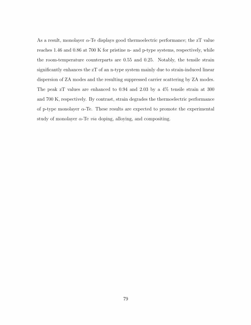
As a result, monolayer α-Te displays good thermoelectric performance; the zT value
reaches 1.46 and 0.86 at 700 K for pristine n- and p-type systems, respectively, while
the room-temperature counterparts are 0.55 and 0.25. Notably, the tensile strain
significantly enhances the zT of an n-type system mainly due to strain-induced linear
dispersion of ZA modes and the resulting suppressed carrier scattering by ZA modes.
The peak zT values are enhanced to 0.94 and 2.03 by a 4% tensile strain at 300
and 700 K, respectively. By contrast, strain degrades the thermoelectric performance
of p-type monolayer α-Te. These results are expected to promote the experimental
study of monolayer α-Te via doping, alloying, and compositing.
79
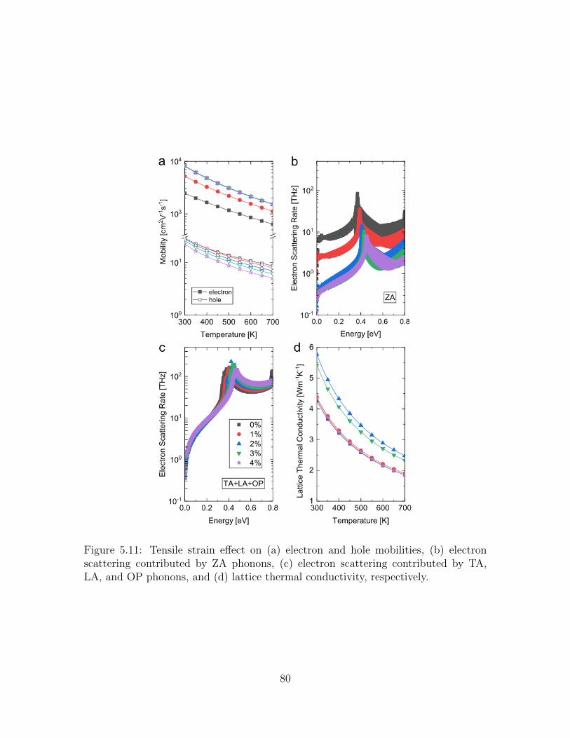
Figure 5.11: Tensile strain effect on (a) electron and hole mobilities, (b) electronscattering contributed by ZA phonons, (c) electron scattering contributed by TA,LA, and OP phonons, and (d) lattice thermal conductivity, respectively.
80
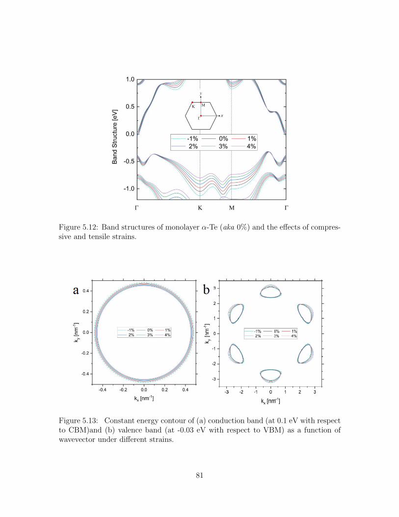
Figure 5.12: Band structures of monolayer α-Te (aka 0%) and the effects of compres-sive and tensile strains.
Figure 5.13: Constant energy contour of (a) conduction band (at 0.1 eV with respectto CBM)and (b) valence band (at -0.03 eV with respect to VBM) as a function ofwavevector under different strains.
81

Figure 5.14: Phonon dispersions of monolayer α-Te (aka 0%) and the effects of com-pressive and tensile strains.
Figure 5.15: Scattering rates of holes contributed by ZA phonons and other phononmodes under different tensile strains at room temperature.
82
Figure 5.16: Effects of compressive strain on the electron and hole mobilities of mono-layer α-Te at different temperatures.
Figure 5.17: Effects of compressive strain on the scattering rates of electrons con-tributed by ZA phonons and other phonon modes at room temperature.
83

Figure 5.18: Concentration dependence of the zT for (a) n- and (b) p-type α-Te underdifferent tensile strains at 300 and 700 K, respectively.
84

Figure 5.19: Maximum zT under different tensile strains for n- and p-type alpha-Teat different temperatures.
85
Chapter 6
Conclusions and Future Work
In this dissertation, we presented our home-developed algorithms based on
Boltzmann transport equation in conjunction with electron-phonon interactions for
calculating the electrical transport properties, such as electrical conductivity, electri-
cal thermal conductivity, Seebeck coefficient. Our scheme combined with the available
methods for phonon transport properties (aka lattice thermal conductivity) can pro-
vide a complete description of the thermoelectric figure of merit.
When examining the correctness of our methodology, the calculated mobilities
for both n-type and p-type 3C-SiC are consistent with the experimental data. In
addition, it is interesting to find a temperature scattering mechanism for both types of
charge carriers. At room temperature, the scattering is dominated by the longitudinal
acoustic (LA) phonons. However, at elevated temperature, the polar longitudinal
optical (LO) phonons become dominant. This is because of the high frequency of the
LO phonons, which are less populated at room temperature.
We found that the anisotropy of the effective mass is greatly related to the
anisotropic electrical conductivity and electrical thermal conductivity in the study of
Mg3Sb2 in Chapter 4. Strong anisotropic electrical conductivity and electrical thermal
86
conductivity were observed in p-type Mg3Sb2, whereas they are nearly isotropic in the
n-type counterpart. Seebeck coefficient and lattice thermal conductivity tend to be
nearly isotropic in both types. Therefore, strong anisotropic thermoelectric properties
were found for p-type Mg3Sb2. And it is interesting to note the thermoelectric figure
of merit along the out-of-plane direction is above unity, indicating that the p-type
performance might be improved experimentally.
Our methodology can also be used for calculating the thermoelectric properties
of two-dimensional materials. In Chapter 5, ultrahigh electron mobility is obtained
for α-Te. However, the hole mobility is two orders of magnitude smaller. In addition,
it is noticeable that the lattice thermal conductivity of α-Te is lower than many
previously reported two-dimensional materials due to its low phonon frequency and
short phonon lifetime. Above room temperature, the lattice thermal conductivity
is lower than 4.2 Wm−1K−1. As a result, two-dimensional α-Te exhibits excellent
thermoelectric performance; the zT value reaches 1.46 and 0.86 at 700 K for pristine
n- and p-type systems, respectively. Besides, even small tensile strain (up to 4%) can
significantly enhance the zT of an n-type system mainly due to strain-induced linear
dispersion of ZA modes and the resulting suppressed carrier scattering by ZA modes.
The peak zT values are enhanced to 0.94 and 2.03 by a 4% tensile strain at 300 and
700 K, respectively. By contrast, strain degrades the thermoelectric performance of
p-type monolayer α-Te.
The recent development on the thermoelectric properties of Dirac/Weyl nodal
semimetal brings in a new viewpoint for the thermoelectric materials. [224, 225, 226,
227, 228, 228] For example, the maximum zT of Cd3As2 could achieve 1.24 at 450 K
under magnetic field of 9 T, which is order of magnitude higher than the data obtained
with the absence of magnetic field. [225] However, compared to the fast development
of the experimental techniques, the theoretical approaches are being developed at a
87
slower pace. [229, 230] Most importantly, all the theoretical/computational research
did not consider the electron-phonon interaction, which is the main source of scat-
tering especially at temperature well above the Debye temperature of the material.
Therefore, the thermoelectric transport properties of Dirac/Weyl nodal semimetal
still warrant further studies from the theoretical/computational viewpoint. In fu-
ture work, the effects from magnetic field need to be considered in the algorithms,
in which the magnetic field would be an adjustable parameter so that we would be
able to calculate the thermoelectric properties under magnetic field directly from first
principles, which can provide fruitful physical insights of the detailed thermoelectric
transport mechanism under magnetic field.
88

Appendices
89
Appendix A Phonon-Isotope Scattering
In single crystals, besides from phonon-phonon interactions, phonons can also
be scattered by isotopes. [57] The phonon-isotope scattering rate can be calculated
with [231, 232]
Γλλ′ =πω2
2
∑i∈u.c.
g(i)|e∗λ(i)eλ′(i)|2δ(ωλ − ωλ′) (A.1)
where λ denote the phonon index with q point and p branch. In Equation A.1, the
g(i) is the Pearson deviation coefficient for each atom in the primitive unit cell, and
can be obtained as:
g(i) =∑s
fs(i)[1−Ms(i)/M(i)]2 (A.2)
where fs is the relative frequency with 0 < fx ≤ 1, Ms(i) represent the mass of isotope
s for the element corresponding to atom i and their average M(i) is given by:
M(i) =∑s
fsMs(i). (A.3)
90
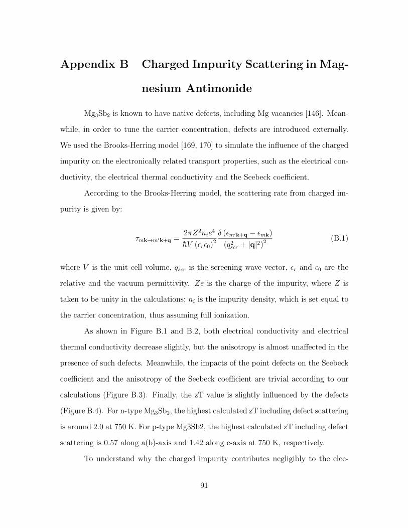
Appendix B Charged Impurity Scattering in Mag-
nesium Antimonide
Mg3Sb2 is known to have native defects, including Mg vacancies [146]. Mean-
while, in order to tune the carrier concentration, defects are introduced externally.
We used the Brooks-Herring model [169, 170] to simulate the influence of the charged
impurity on the electronically related transport properties, such as the electrical con-
ductivity, the electrical thermal conductivity and the Seebeck coefficient.
According to the Brooks-Herring model, the scattering rate from charged im-
purity is given by:
τmk→m′k+q =2πZ2nie
4
hV (εrε0)2
δ (εm′k+q − εmk)
(q2scr + |q|2)2 (B.1)
where V is the unit cell volume, qscr is the screening wave vector, εr and ε0 are the
relative and the vacuum permittivity. Ze is the charge of the impurity, where Z is
taken to be unity in the calculations; ni is the impurity density, which is set equal to
the carrier concentration, thus assuming full ionization.
As shown in Figure B.1 and B.2, both electrical conductivity and electrical
thermal conductivity decrease slightly, but the anisotropy is almost unaffected in the
presence of such defects. Meanwhile, the impacts of the point defects on the Seebeck
coefficient and the anisotropy of the Seebeck coefficient are trivial according to our
calculations (Figure B.3). Finally, the zT value is slightly influenced by the defects
(Figure B.4). For n-type Mg3Sb2, the highest calculated zT including defect scattering
is around 2.0 at 750 K. For p-type Mg3Sb2, the highest calculated zT including defect
scattering is 0.57 along a(b)-axis and 1.42 along c-axis at 750 K, respectively.
To understand why the charged impurity contributes negligibly to the elec-
91
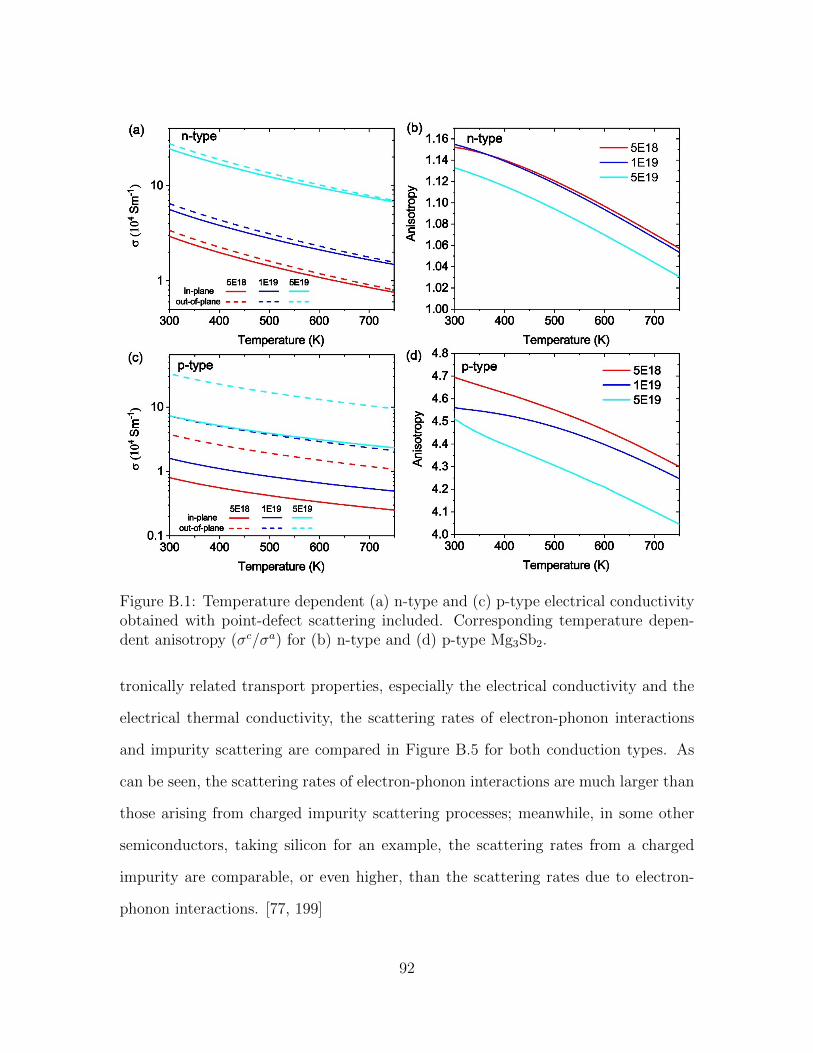
Figure B.1: Temperature dependent (a) n-type and (c) p-type electrical conductivityobtained with point-defect scattering included. Corresponding temperature depen-dent anisotropy (σc/σa) for (b) n-type and (d) p-type Mg3Sb2.
tronically related transport properties, especially the electrical conductivity and the
electrical thermal conductivity, the scattering rates of electron-phonon interactions
and impurity scattering are compared in Figure B.5 for both conduction types. As
can be seen, the scattering rates of electron-phonon interactions are much larger than
those arising from charged impurity scattering processes; meanwhile, in some other
semiconductors, taking silicon for an example, the scattering rates from a charged
impurity are comparable, or even higher, than the scattering rates due to electron-
phonon interactions. [77, 199]
92
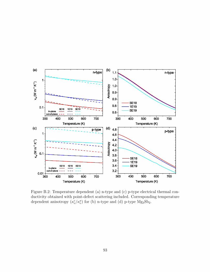
Figure B.2: Temperature dependent (a) n-type and (c) p-type electrical thermal con-ductivity obtained with point-defect scattering included. Corresponding temperaturedependent anisotropy (κce/κ
ae) for (b) n-type and (d) p-type Mg3Sb2.
93
Figure B.3: Temperature dependent (a) n-type and (c) p-type Seebeck coefficient ob-tained with point-defect scattering included. Corresponding temperature dependentanisotropy (αc/αa) for (b) n-type and (d) p-type Mg3Sb2.
94
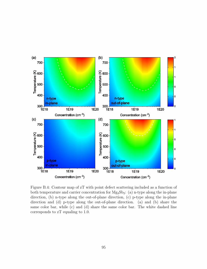
Figure B.4: Contour map of zT with point defect scattering included as a function ofboth temperature and carrier concentration for Mg3Sb2: (a) n-type along the in-planedirection, (b) n-type along the out-of-plane direction, (c) p-type along the in-planedirection and (d) p-type along the out-of-plane direction. (a) and (b) share thesame color bar, while (c) and (d) share the same color bar. The white dashed linecorresponds to zT equaling to 1.0.
95
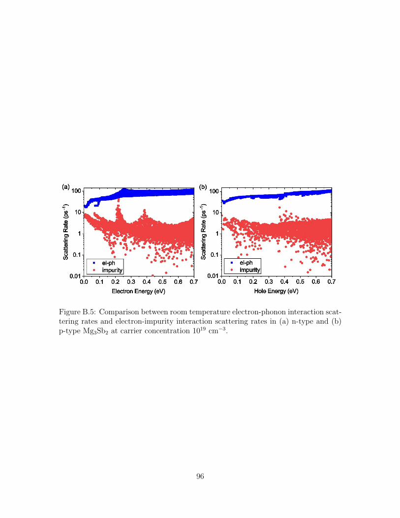
Figure B.5: Comparison between room temperature electron-phonon interaction scat-tering rates and electron-impurity interaction scattering rates in (a) n-type and (b)p-type Mg3Sb2 at carrier concentration 1019 cm−3.
96
Appendix C Convergence Check for Lattice Ther-
mal Conductivity for Two Dimensional
alpha-Tellurium
The first principles calculation of lattice thermal conductivity using ShengBTE
package [58] requires several convergence checks. In convention, a truncating cutoff is
implemented in the calculations of third-order anharmonic interatomic force constants
(IFCs). We have checked that a cutoff distance of 0.6 nm, used in our work, can
achieve reasonable convergence. As shown in Figure C.1(a), if the cutoff is not large
enough, the lattice thermal conductivity would be overestimated.
When applying ShengBTE package to solve BTE, there are two more parame-
ters affecting the convergence, namely, ngrids and scalebroad. The ngrids denotes the
q meshes of Brillouin zone, whereas the scalebroad controls the energy conservation
process. We first used a safely large scalebroad = 1 to check the convergence with
respect to q grids, and found that the lattice thermal conductivity is easily converged,
as shown in Figure C.1(b). Then, using large q grids, we checked the convergence
with respect to the scalebroad. As a routine, one uses a small scalebroad to reduce
the processes that need to be considered to save the computational cost. However,
we found that the scalebroad should be larger than 0.1, otherwise small scalebroad
would overestimate the lattice thermal conductivity, as shown in Figure C.1(c).
To have a deeper understanding of the overestimation caused by a small scale-
broad value, here we calculated the frequency-dependent contribution to the lattice
thermal conductivity, as what was done in the work of Gao et al. [195]. As shown in
Figure S4, it is found that the overestimation mainly comes from the non-convergent
low-frequency phonons. With a small scalebroad, we reproduced the low-frequency
97

peak reported in the work of Gao et al. [195] However, using convergent scalebroad,
the peak is gone, and the distribution lines converge very well.
Therefore, in this work, we use a cutoff of 0.6 nm for the calculation of third
order IFCs, and in solving BTE, we use 200×200×1 q grids with scalebroad=1.
Figure C.1: Convergence of lattice thermal conductivity with respect to (a) the cutoffdistance for third-order IFCs, (b) the q grids, and (c) the scalebroad, at room tem-perature.
98

Figure C.2: Contribution to the lattice thermal conductivity from different frequenciesat room temperature with different scalebroad parameters.
99
Appendix D Tensile Strain Effect on Thermoelec-
tric Properties Two Dimensional alpha-
Tellurium
The tensile strain effect on Seebeck coefficient, electrical conductivity, elec-
tronic thermal conductivity, and power factor for n- and p-type α-Te are given in
Figures D.1 and D.2, respectively. Overall, the Seebeck coefficient is weakly affected
by tensile strain in both n-type and p-type systems. The electrical conductivity, elec-
tronic thermal conductivity, and power factor in n-type system first increase obviously
when the strain changes from 0 to 2% and then remain almost unchanged as strain
increases from 2% to 4%, whereas these properties are decreased in p-type system
with strain changing from 0 to 4%, which is consistent with the changing trends of
mobilities.
100
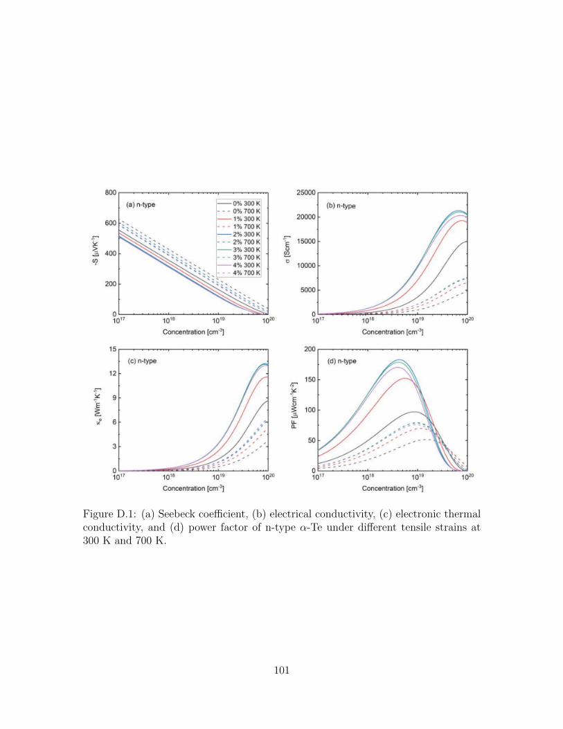
Figure D.1: (a) Seebeck coefficient, (b) electrical conductivity, (c) electronic thermalconductivity, and (d) power factor of n-type α-Te under different tensile strains at300 K and 700 K.
101
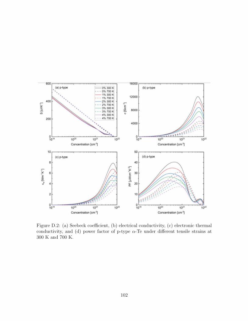
Figure D.2: (a) Seebeck coefficient, (b) electrical conductivity, (c) electronic thermalconductivity, and (d) power factor of p-type α-Te under different tensile strains at300 K and 700 K.
102
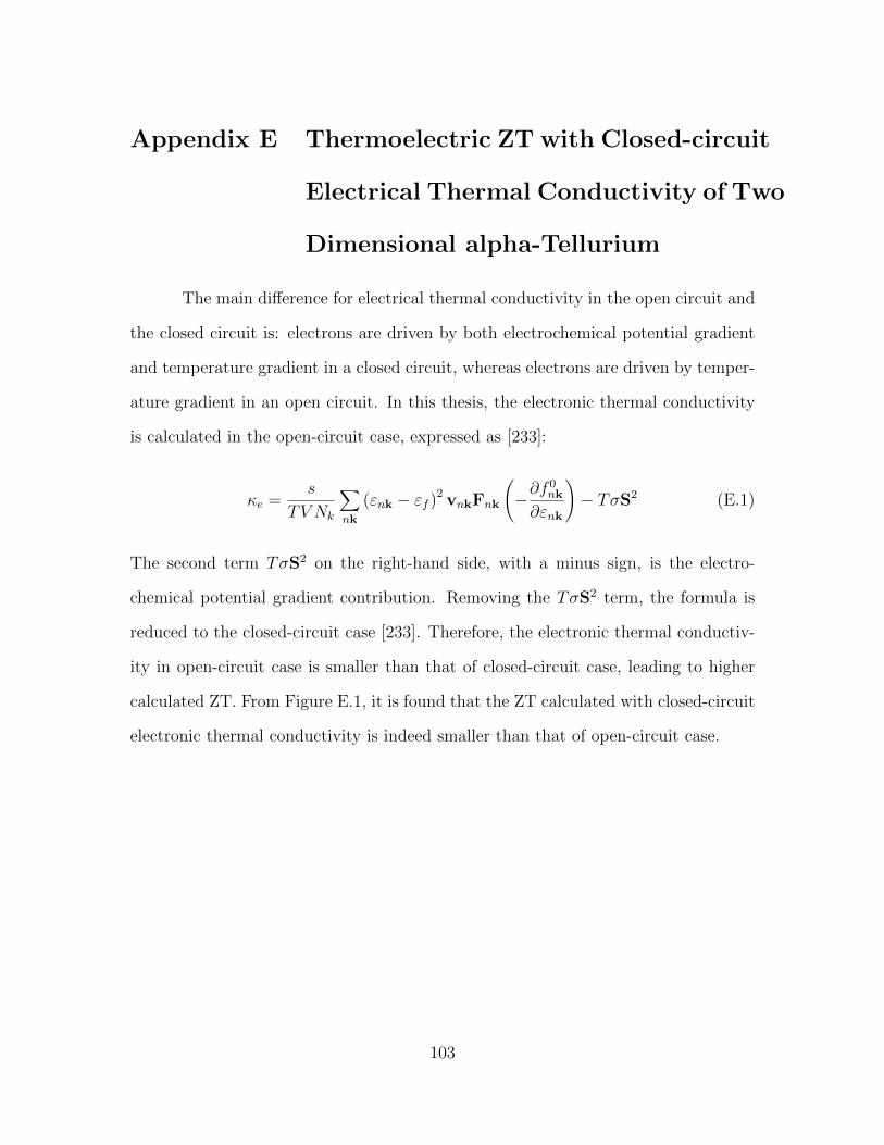
Appendix E Thermoelectric ZT with Closed-circuit
Electrical Thermal Conductivity of Two
Dimensional alpha-Tellurium
The main difference for electrical thermal conductivity in the open circuit and
the closed circuit is: electrons are driven by both electrochemical potential gradient
and temperature gradient in a closed circuit, whereas electrons are driven by temper-
ature gradient in an open circuit. In this thesis, the electronic thermal conductivity
is calculated in the open-circuit case, expressed as [233]:
κe =s
TV Nk
∑nk
(εnk − εf )2 vnkFnk
(−∂f
0nk
∂εnk
)− TσS2 (E.1)
The second term TσS2 on the right-hand side, with a minus sign, is the electro-
chemical potential gradient contribution. Removing the TσS2 term, the formula is
reduced to the closed-circuit case [233]. Therefore, the electronic thermal conductiv-
ity in open-circuit case is smaller than that of closed-circuit case, leading to higher
calculated ZT. From Figure E.1, it is found that the ZT calculated with closed-circuit
electronic thermal conductivity is indeed smaller than that of open-circuit case.
103
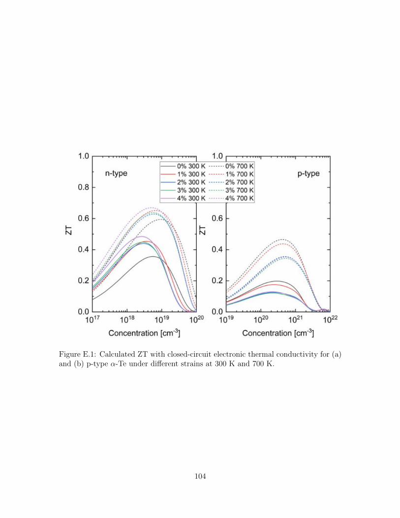
Figure E.1: Calculated ZT with closed-circuit electronic thermal conductivity for (a)and (b) p-type α-Te under different strains at 300 K and 700 K.
104
Bibliography
[1] Timothy D. Sands. Designing nanocomposite thermoelectric materials,https://nanohub.org/resources/383, Nov 2005.
[2] Safa O Kasap. Principles of electronic materials and devices. McGraw-Hill,2006.
[3] Jing-Feng Li, Wei-Shu Liu, Li-Dong Zhao, and Min Zhou. High-performancenanostructured thermoelectric materials. NPG Asia Materials, 2(4):152–158,2010.
[4] Cheryl Sturm, Parisa Jafarzadeh, and Holger Kleinke. 1.17 thermoelectric nano-materials. Comprehensive Nanoscience and Nanotechnology, page 349, 2019.
[5] http://thermoelectrics.matsci.northwestern.edu/thermoelectrics/.
[6] Yanzhong Pei, Xiaoya Shi, Aaron LaLonde, Heng Wang, Lidong Chen, andG Jeffrey Snyder. Convergence of electronic bands for high performance bulkthermoelectrics. Nature, 473(7345):66–69, 2011.
[7] J Serrano, J Strempfer, M Cardona, M Schwoerer-Bohning, H Requardt,M Lorenzen, B Stojetz, P Pavone, and WJ Choyke. Determination of thephonon dispersion of zinc blende (3C) silicon carbide by inelastic x-ray scatter-ing. Applied physics letters, 80(23):4360–4362, 2002.
[8] F Widulle, T Ruf, O Buresch, A Debernardi, and M Cardona. Raman studyof isotope effects and phonon eigenvectors in SiC. Physical review letters,82(15):3089, 1999.
[9] WE Nelson, FA Halden, and A Rosengreen. Growth and properties of β-sicsingle crystals. Journal of Applied Physics, 37(1):333–336, 1966.
[10] Mikiya Shinohara, Mitsugu Yamanaka, Hiroshi Daimon, Eiichiro Sakuma, Ha-jime Okumura, Shunji Misawa, Kazuhiro Endo, and Sadafumi Yoshida. Growthof high-mobility 3C-SiC epilayers by chemical vapor deposition. Japanese jour-nal of applied physics, 27(3A):L434, 1988.
105
[11] AA Lebedev, PL Abramov, EV Bogdanova, SP Lebedev, DK Nel’son,GA Oganesyan, AS Tregubova, and Rositsa Yakimova. Highly doped p-type 3C-SiC on 6H-SiC substrates. Semiconductor Science and Technology,23(7):075004, 2008.
[12] Soohyun Kim, Chungman Kim, Yang-Ki Hong, Takahiro Onimaru, KoichiroSuekuni, Toshiro Takabatake, and Myung-Hwa Jung. Thermoelectric proper-ties of Mn-doped Mg-Sb single crystals. Journal of Materials Chemistry A,2(31):12311–12316, 2014.
[13] Soo Hyun Kim, Chung Man Kim, Yang-Ki Hong, Kyung Ik Sim, Jae HoonKim, Takahiro Onimaru, Toshiro Takabatake, and Myung-Hwa Jung. Thermo-electric properties of Mg3Sb2−xBix single crystals grown by Bridgman method.Materials Research Express, 2(5):055903, 2015.
[14] Jiazhan Xin, Guowei Li, Gudrun Auffermann, Horst Borrmann, WalterSchnelle, Johannes Gooth, Xinbing Zhao, Tiejun Zhu, Claudia Felser, andChenguang Fu. Growth and transport properties of Mg3X2 (X= Sb, Bi) singlecrystals. Materials Today Physics, 7:61–68, 2018.
[15] Lirong Song, Jiawei Zhang, and Bo B Iversen. Simultaneous improvement ofpower factor and thermal conductivity via Ag doping in p-type Mg3Sb2 ther-moelectric materials. Journal of Materials Chemistry a, 5(10):4932–4939, 2017.
[16] A Bhardwaj, NS Chauhan, and DK Misra. Significantly enhanced thermoelec-tric figure of merit of p-type Mg3Sb2-based Zintl phase compounds via nanos-tructuring and employing high energy mechanical milling coupled with sparkplasma sintering. Journal of Materials Chemistry A, 3(20):10777–10786, 2015.
[17] Shan Huang, Ziyu Wang, Rui Xiong, Hongyu Yu, and Jing Shi. Signifi-cant enhancement in thermoelectric performance of Mg3Sb2 from bulk to two-dimensional mono layer. Nano Energy, 62:212–219, 2019.
[18] Jiawei Zhang, Lirong Song, Mattia Sist, Kasper Tolborg, and Bo BrummerstedtIversen. Chemical bonding origin of the unexpected isotropic physical proper-ties in thermoelectric Mg3Sb2 and related materials. Nature communications,9(1):1–10, 2018.
[19] Jiawei Zhang, Lirong Song, Steffen Hindborg Pedersen, Hao Yin, Bo Brummer-stedt Iversen, et al. Discovery of high-performance low-cost n-type Mg3Sb2-based thermoelectric materials with multi-valley conduction bands. Naturecommunications, 8(1):1–8, 2017.
106
[20] Jiawei Zhang, Lirong Song, Aref Mamakhel, Mads Ry Vogel Jørgensen, andBo Brummerstedt Iversen. High-performance low-cost n-type Se-doped Mg3Sb2-based Zintl compounds for thermoelectric application. Chemistry of Materials,29(12):5371–5383, 2017.
[21] Hiromasa Tamaki, Hiroki K Sato, and Tsutomu Kanno. Isotropic conductionnetwork and defect chemistry in Mg3+δSb2-based layered Zintl compounds withhigh thermoelectric performance. Advanced Materials, 28(46):10182–10187,2016.
[22] Jun Mao, Yixuan Wu, Shaowei Song, Qing Zhu, Jing Shuai, Zihang Liu,Yanzhong Pei, and Zhifeng Ren. Defect engineering for realizing high thermo-electric performance in n-type Mg3Sb2-based materials. ACS Energy Letters,2(10):2245–2250, 2017.
[23] Jing Shuai, Yumei Wang, Hee Seok Kim, Zihang Liu, Jingying Sun, Shuo Chen,Jiehe Sui, and Zhifeng Ren. Thermoelectric properties of Na-doped Zintl com-pound: Mg3−xNaxSb2. Acta Materialia, 93:187–193, 2015.
[24] Chen Chen, Xiaofang Li, Shan Li, Xinyu Wang, Zongwei Zhang, Jiehe Sui, FengCao, Xingjun Liu, and Qian Zhang. Enhanced thermoelectric performance ofp-type Mg3Sb2 by lithium doping and its tunability in an anionic framework.Journal of Materials Science, 53(23):16001–16009, 2018.
[25] Hao Wang, Jin Chen, Tianqi Lu, Kunjie Zhu, Shan Li, Jun Liu, and HuaizhouZhao. Enhanced thermoelectric performance in p-type Mg3Sb2 via lithium dop-ing. Chinese Physics B, 27(4):047212, 2018.
[26] Xiaodan Tang, Bin Zhang, Xiao Zhang, Shuxia Wang, Xu Lu, Guang Han,Guoyu Wang, and Xiaoyuan Zhou. Enhancing the thermoelectric performanceof p-type Mg3Sb2 via codoping of Li and Cd. ACS Applied Materials & Inter-faces, 12(7):8359–8365, 2020.
[27] Jun Mao, Jing Shuai, Shaowei Song, Yixuan Wu, Rebecca Dally, Jiawei Zhou,Zihang Liu, Jifeng Sun, Qinyong Zhang, Clarina Dela Cruz, et al. Manipulationof ionized impurity scattering for achieving high thermoelectric performancein n-type Mg3Sb2-based materials. Proceedings of the National Academy ofSciences, 114(40):10548–10553, 2017.
[28] Kazuki Imasato, Max Wood, Jimmy Jiahong Kuo, and G Jeffrey Snyder.Improved stability and high thermoelectric performance through cation sitedoping in n-type La-doped Mg3Sb1.5Bi0.5. Journal of Materials Chemistry A,6(41):19941–19946, 2018.
107

[29] Xuemin Shi, Tingting Zhao, Xinyue Zhang, Cheng Sun, Zhiwei Chen, Siqi Lin,Wen Li, Hui Gu, and Yanzhong Pei. Extraordinary n-type Mg3SbBi thermo-electrics enabled by yttrium doping. Advanced Materials, 31(36):1903387, 2019.
[30] Tsutomu Kanno, Hiromasa Tamaki, Hiroki K Sato, Stephen Dongmin Kang,Saneyuki Ohno, Kazuki Imasato, Jimmy Jiahong Kuo, G Jeffrey Snyder, andYuzuru Miyazaki. Enhancement of average thermoelectric figure of merit byincreasing the grain-size of Mg3.2Sb1.5Bi0.49Te0.01. Applied Physics Letters,112(3):033903, 2018.
[31] TJ Seebeck. The magnetic polarization of metals and ores produced by temper-ature difference. Proceedings. of Prussian Academy of Sciences, pages 265–373,1822.
[32] JCA Peltier. New experiments on the heat effects of electric currents (inFrench). Ann. Chim. Phys, 56:371–386, 1834.
[33] H Julian Goldsmid. The Seebeck and Peltier effects. The Physics of Thermo-electric Energy Conversion, pages 2053–2571, 2017.
[34] Jae Sung Lee and Hyunggyu Park. Carnot efficiency is reachable in an irre-versible process. Scientific reports, 7(1):1–9, 2017.
[35] G Jeffrey Snyder and Eric S Toberer. Complex thermoelectric materials. InMaterials for sustainable energy: a collection of peer-reviewed research and re-view articles from Nature Publishing Group, pages 101–110. World Scientific,2011.
[36] Tiejun Zhu, Lipeng Hu, Xinbing Zhao, and Jian He. New insights into in-trinsic point defects in V2VI3 thermoelectric materials. Advanced Science,3(7):1600004, 2016.
[37] Lei Yang, Zhi-Gang Chen, Matthew S Dargusch, and Jin Zou. High performancethermoelectric materials: progress and their applications. Advanced EnergyMaterials, 8(6):1701797, 2018.
[38] Tiejun Zhu, Yintu Liu, Chenguang Fu, Joseph P Heremans, Jeffrey G Snyder,and Xinbing Zhao. Compromise and synergy in high-efficiency thermoelectricmaterials. Advanced materials, 29(14):1605884, 2017.
[39] Min Hong, Wanyu Lyv, Meng Li, Shengduo Xu, Qiang Sun, Jin Zou, andZhi-Gang Chen. Rashba effect maximizes thermoelectric performance of GeTederivatives. Joule, 4(9):2030–2043, 2020.
108
[40] Min Hong, Zhi-Gang Chen, Lei Yang, Yi-Chao Zou, Matthew S Dargusch,Hao Wang, and Jin Zou. Realizing zT of 2.3 in Ge1−x−ySbxInyTe via reduc-ing the phase-transition temperature and introducing resonant energy doping.Advanced materials, 30(11):1705942, 2018.
[41] Joseph P Heremans, Bartlomiej Wiendlocha, and Audrey M Chamoire. Res-onant levels in bulk thermoelectric semiconductors. Energy & EnvironmentalScience, 5(2):5510–5530, 2012.
[42] Joseph P Heremans, Vladimir Jovovic, Eric S Toberer, Ali Saramat, KenKurosaki, Anek Charoenphakdee, Shinsuke Yamanaka, and G Jeffrey Snyder.Enhancement of thermoelectric efficiency in PbTe by distortion of the electronicdensity of states. Science, 321(5888):554–557, 2008.
[43] Qinyong Zhang, Hui Wang, Weishu Liu, Hengzhi Wang, Bo Yu, Qian Zhang,Zhiting Tian, George Ni, Sangyeop Lee, Keivan Esfarjani, et al. Enhancementof thermoelectric figure-of-merit by resonant states of aluminium doping in leadselenide. Energy & Environmental Science, 5(1):5246–5251, 2012.
[44] Qian Zhang, Bolin Liao, Yucheng Lan, Kevin Lukas, Weishu Liu, Keivan Es-farjani, Cyril Opeil, David Broido, Gang Chen, and Zhifeng Ren. High ther-moelectric performance by resonant dopant indium in nanostructured SnTe.Proceedings of the National Academy of Sciences, 110(33):13261–13266, 2013.
[45] Gangjian Tan, Li-Dong Zhao, and Mercouri G Kanatzidis. Rationally de-signing high-performance bulk thermoelectric materials. Chemical reviews,116(19):12123–12149, 2016.
[46] Yufei Liu, Menghan Zhou, and Jian He. Towards higher thermoelectric perfor-mance of Bi2Te3 via defect engineering. Scripta Materialia, 111:39–43, 2016.
[47] Wei Wei, Cheng Chang, Teng Yang, Jizi Liu, Huaichao Tang, Jian Zhang,Yusheng Li, Feng Xu, Zhidong Zhang, Jing-Feng Li, et al. Achieving high ther-moelectric figure of merit in polycrystalline SnSe via introducing Sn vacancies.Journal of the American Chemical Society, 140(1):499–505, 2018.
[48] Wen Li, Siqi Lin, Xinyue Zhang, Zhiwei Chen, Xiangfan Xu, and YanzhongPei. Thermoelectric properties of Cu2SnSe4 with intrinsic vacancy. Chemistryof Materials, 28(17):6227–6232, 2016.
[49] Juan Li, Xinyue Zhang, Siqi Lin, Zhiwei Chen, and Yanzhong Pei. Realizingthe high thermoelectric performance of GeTe by Sb-doping and Se-alloying.Chemistry of Materials, 29(2):605–611, 2017.
109

[50] Jing Tang, Bo Gao, Siqi Lin, Xiao Wang, Xinyue Zhang, Fen Xiong, Wen Li,Yue Chen, and Yanzhong Pei. Manipulation of solubility and interstitial defectsfor improving thermoelectric SnTe alloys. ACS Energy Letters, 3(8):1969–1974,2018.
[51] Kanishka Biswas, Jiaqing He, Ivan D Blum, Chun-I Wu, Timothy P Hogan,David N Seidman, Vinayak P Dravid, and Mercouri G Kanatzidis. High-performance bulk thermoelectrics with all-scale hierarchical architectures. Na-ture, 489(7416):414–418, 2012.
[52] Li-Dong Zhao, Shih-Han Lo, Yongsheng Zhang, Hui Sun, Gangjian Tan, CtiradUher, Christopher Wolverton, Vinayak P Dravid, and Mercouri G Kanatzidis.Ultralow thermal conductivity and high thermoelectric figure of merit in SnSecrystals. Nature, 508(7496):373–377, 2014.
[53] Wen Li, Siqi Lin, Manuel Weiss, Zhiwei Chen, Juan Li, Yidong Xu, Wolf-gang G Zeier, and Yanzhong Pei. Crystal structure induced ultralow latticethermal conductivity in thermoelectric Ag9AlSe6. Advanced Energy Materials,8(18):1800030, 2018.
[54] Xiaolei Shi, Angyin Wu, Weidi Liu, Raza Moshwan, Yuan Wang, Zhi-GangChen, and Jin Zou. Polycrystalline SnSe with extraordinary thermoelectricproperty via nanoporous design. ACS nano, 12(11):11417–11425, 2018.
[55] Weidi Liu, Xiaolei Shi, Raza Moshwan, Min Hong, Lei Yang, Zhi-Gang Chen,and Jin Zou. Enhancing thermoelectric performance of (Cu1−xAgx)2Se viaCuAgSe secondary phase and porous design. Sustainable Materials and Tech-nologies, 17:e00076, 2018.
[56] Siqi Lin, Wen Li, Shasha Li, Xinyue Zhang, Zhiwei Chen, Yidong Xu, Yue Chen,and Yanzhong Pei. High thermoelectric performance of Ag9GaSe6 enabled bylow cutoff frequency of acoustic phonons. Joule, 1(4):816–830, 2017.
[57] John M Ziman. Electrons and phonons: the theory of transport phenomena insolids. Oxford university press, 2001.
[58] Wu Li, Jesus Carrete, Nebil A Katcho, and Natalio Mingo. ShengBTE: Asolver of the Boltzmann transport equation for phonons. Computer PhysicsCommunications, 185(6):1747–1758, 2014.
[59] DA Broido, A Ward, and N Mingo. Lattice thermal conductivity of silicon fromempirical interatomic potentials. Physical Review B, 72(1):014308, 2005.
[60] Aleksandr Chernatynskiy and Simon R Phillpot. Evaluation of computationaltechniques for solving the boltzmann transport equation for lattice thermalconductivity calculations. Physical Review B, 82(13):134301, 2010.
110
[61] David A Broido, Michael Malorny, Gerd Birner, Natalio Mingo, and DA Stew-art. Intrinsic lattice thermal conductivity of semiconductors from first princi-ples. Applied Physics Letters, 91(23):231922, 2007.
[62] Alistair Ward, DA Broido, Derek A Stewart, and Gernot Deinzer. Ab initiotheory of the lattice thermal conductivity in diamond. Physical Review B,80(12):125203, 2009.
[63] DA Broido, L Lindsay, and A Ward. Thermal conductivity of diamond underextreme pressure: A first-principles study. Physical Review B, 86(11):115203,2012.
[64] L Lindsay, DA Broido, and TL Reinecke. Thermal conductivity and large iso-tope effect in GaN from first principles. Physical review letters, 109(9):095901,2012.
[65] Wu Li, Lucas Lindsay, David A Broido, Derek A Stewart, and Natalio Mingo.Thermal conductivity of bulk and nanowire Mg2SixSn1−x alloys from first prin-ciples. Physical Review B, 86(17):174307, 2012.
[66] John Bardeen, Leon N Cooper, and John Robert Schrieffer. Theory of super-conductivity. Physical review, 108(5):1175, 1957.
[67] W Kohn. Image of the Fermi surface in the vibration spectrum of a metal.Physical Review Letters, 2(9):393, 1959.
[68] Rudolf Ernst Peierls. Quantum theory of solids. Clarendon Press, 1996.
[69] Andrea Damascelli, Zahid Hussain, and Zhi-Xun Shen. Angle-resolved photoe-mission studies of the cuprate superconductors. Reviews of modern physics,75(2):473, 2003.
[70] L Pintschovius. Electron-phonon coupling effects explored by inelastic neutronscattering. physica status solidi (b), 242(1):30–50, 2005.
[71] Emmanouil Kioupakis, Patrick Rinke, Andre Schleife, Friedhelm Bechstedt, andChris G Van de Walle. Free-carrier absorption in nitrides from first principles.Physical Review B, 81(24):241201, 2010.
[72] Jesse Noffsinger, Emmanouil Kioupakis, Chris G Van de Walle, Steven G Louie,and Marvin L Cohen. Phonon-assisted optical absorption in silicon from firstprinciples. Physical review letters, 108(16):167402, 2012.
[73] Marios Zacharias, Christopher E Patrick, and Feliciano Giustino. Stochas-tic approach to phonon-assisted optical absorption. Physical review letters,115(17):177401, 2015.
111
[74] Manuel Cardona and Mike LW Thewalt. Isotope effects on the optical spectraof semiconductors. Reviews of modern physics, 77(4):1173, 2005.
[75] NF Mott. The conductivity of metals. Proceedings of the Physical Society,46(5):680, 1934.
[76] David Keith Chalmers MacDonald. Thermoelectricity: an introduction to theprinciples. Courier Corporation, 2006.
[77] Wu Li. Electrical transport limited by electron-phonon coupling from boltz-mann transport equation: An ab initio study of Si, Al, and MoS2. PhysicalReview B, 92(7):075405, 2015.
[78] M Omini and A Sparavigna. An iterative approach to the phonon Boltzmannequation in the theory of thermal conductivity. Physica B: Condensed Matter,212(2):101–112, 1995.
[79] L Lindsay, DA Broido, and TL Reinecke. Ab initio thermal transport in com-pound semiconductors. Physical Review B, 87(16):165201, 2013.
[80] Te-Huan Liu, Jiawei Zhou, Bolin Liao, David J Singh, and Gang Chen. First-principles mode-by-mode analysis for electron-phonon scattering channels andmean free path spectra in GaAs. Physical Review B, 95(7):075206, 2017.
[81] Jinlong Ma, Arun S Nissimagoudar, and Wu Li. First-principles study of elec-tron and hole mobilities of Si and GaAs. Physical Review B, 97(4):045201,2018.
[82] Te-Huan Liu, Bai Song, Laureen Meroueh, Zhiwei Ding, Qichen Song, JiaweiZhou, Mingda Li, and Gang Chen. Simultaneously high electron and holemobilities in cubic boron-V compounds: BP, BAs, and BSb. Physical ReviewB, 98(8):081203, 2018.
[83] Samuel Ponce, Elena R Margine, and Feliciano Giustino. Towards predictivemany-body calculations of phonon-limited carrier mobilities in semiconductors.Physical Review B, 97(12):121201, 2018.
[84] Jesse Noffsinger, Feliciano Giustino, Brad D Malone, Cheol-Hwan Park,Steven G Louie, and Marvin L Cohen. EPW: A program for calculating theelectron-phonon coupling using maximally localized Wannier functions. Com-puter Physics Communications, 181(12):2140–2148, 2010.
[85] Samuel Ponce, Elena R Margine, Carla Verdi, and Feliciano Giustino. EPW:Electron-phonon coupling, transport and superconducting properties usingmaximally localized Wannier functions. Computer Physics Communications,209:116–133, 2016.
112

[86] Philip B Allen. Improved callaway model for lattice thermal conductivity. Phys-ical Review B, 88(14):144302, 2013.
[87] WJ Choyke and G Pensl. Physical properties of SiC. Mrs Bulletin, 22(3):25–29,1997.
[88] Lyle Patrick, DR Hamilton, and WJ Choyke. Growth, luminescence, selec-tion rules, and lattice sums of SiC with wurtzite structure. Physical Review,143(2):526, 1966.
[89] Philip G Neudeck. Progress in silicon carbide semiconductor electronics tech-nology. Journal of Electronic Materials, 24(4):283–288, 1995.
[90] Tianshi Wang, Zhigang Gui, Anderson Janotti, Chaoying Ni, and PrashantKarandikar. Strong effect of electron-phonon interaction on the lattice thermalconductivity in 3C-SiC. Physical Review Materials, 1(3):034601, 2017.
[91] Feng Yan, Jian H Zhao, and Gregory H Olsen. Demonstration of the first4H-SiC avalanche photodiodes. Solid-State Electronics, 44(2):341–346, 2000.
[92] YH Zhu, JC Zhang, ZT Chen, and T Egawa. Demonstration on GaN-basedlight-emitting diodes grown on 3C-SiC/Si (111). Journal of Applied Physics,106(12):124506, 2009.
[93] KP Schoen, Jerry M Woodall, James A Cooper, and Michael R Melloch. Designconsiderations and experimental analysis of high-voltage SiC Schottky barrierrectifiers. IEEE Transactions on electron devices, 45(7):1595–1604, 1998.
[94] P Alexandrov, JH Zhao, W Wright, M Pan, and M Weiner. Demonstrationof 140 A, 800 V 4H-SiC pin/Schottky barrier diodes with multi-step junctiontermination extension structures. Electronics Letters, 37(18):1139–1140, 2001.
[95] PA Ivanov, ME Levinshtein, AK Agarwal, and JW Palmour. Transient charac-teristics of a 1.8 kV, 3.8 a 4H-SiC bipolar junction transistor. Semiconductorscience and technology, 16(6):521, 2001.
[96] Anant K Agarwal, Pavel A Ivanov, Michael E Levinshtein, John W Palmour,Sergey L Rumyantsev, and Sei-Hyung Ryu. Turn-off performance of 2.6 kV4H-SiC asymmetrical GTO thyristor. Semiconductor science and technology,16(4):260, 2001.
[97] Michael E Levinshtein, Tigran T Mnatsakanov, Pavel A Ivanov, Anant K Agar-wal, John W Palmour, Sergey L Rumyantsev, Aleksey G Tandoev, and Sergey NYurkov. Temperature dependence of turn-on processes in 4H-SiC thyristors.Solid-State Electronics, 45(3):453–459, 2001.
113

[98] Mohit Bhatnagar and B Jayant Baliga. Comparison of 6H-SiC, 3C-SiC, and Sifor power devices. IEEE Transactions on electron devices, 40(3):645–655, 1993.
[99] M Yamanaka, H Daimon, E Sakuma, S Misawa, and S Yoshida. Temperaturedependence of electrical properties of n-and p-type 3C-SiC. Journal of appliedphysics, 61(2):599–603, 1987.
[100] T Tachibana, HS Kong, YC Wang, and RF Davis. Hall measurements as afunction of temperature on monocrystalline SiC thin films. Journal of appliedphysics, 67(10):6375–6381, 1990.
[101] Matthias Roschke and Frank Schwierz. Electron mobility models for 4H, 6H,and 3C SiC [MESFETs]. IEEE Transactions on Electron Devices, 48(7):1442–1447, 2001.
[102] H-E Nilsson, U Englund, Mats Hjelm, E Bellotti, and K Brennan. Full bandMonte Carlo study of high field transport in cubic phase silicon carbide. Journalof applied physics, 93(6):3389–3394, 2003.
[103] TT Mnatsakanov, LI Pomortseva, and SN Yurkov. Semiempirical model ofcarrier mobility in silicon carbide for analyzing its dependence on temperatureand doping level. Semiconductors, 35(4):394–397, 2001.
[104] Enrico Bellotti, Hans-Erik Nilsson, Kevin F Brennan, and P Paul Ruden. En-semble monte carlo calculation of hole transport in bulk 3C-SiC. Journal ofapplied physics, 85(6):3211–3217, 1999.
[105] Rimvydas Mickevicius and Jian H Zhao. Monte carlo study of electron transportin SiC. Journal of applied physics, 83(6):3161–3167, 1998.
[106] RP Joshi and DK Ferry. Calculations of the temperature and field dependentelectronic mobility in β-SiC. Solid-State Electronics, 38(11):1911–1916, 1995.
[107] K Tsukioka, D Vasileska, and DK Ferry. An ensemble monte carlo study ofhigh-field transport in β-SiC. Physica B: Condensed Matter, 185(1-4):466–470,1993.
[108] Hubert Jan Van Daal. Mobility of charge carriers in silicon carbide. PhilipsResearch Laboratories, 1965.
[109] Carla Verdi and Feliciano Giustino. Frohlich electron-phonon vertex from firstprinciples. Physical review letters, 115(17):176401, 2015.
[110] Jin-Jian Zhou and Marco Bernardi. Ab initio electron mobility and polarphonon scattering in GaAs. Physical Review B, 94(20):201201, 2016.
114
[111] Jinlong Ma, Yani Chen, and Wu Li. Intrinsic phonon-limited charge carriermobilities in thermoelectric SnSe. Physical Review B, 97(20):205207, 2018.
[112] Te-Huan Liu, Jiawei Zhou, Mingda Li, Zhiwei Ding, Qichen Song, Bolin Liao,Liang Fu, and Gang Chen. Electron mean-free-path filtering in dirac materialfor improved thermoelectric performance. Proceedings of the National Academyof Sciences, 115(5):879–884, 2018.
[113] J Sjakste, N Vast, M Calandra, and F Mauri. Wannier interpolation of theelectron-phonon matrix elements in polar semiconductors: Polar-optical cou-pling in GaAs. Physical Review B, 92(5):054307, 2015.
[114] Paolo Giannozzi, Stefano Baroni, Nicola Bonini, Matteo Calandra, RobertoCar, Carlo Cavazzoni, Davide Ceresoli, Guido L Chiarotti, Matteo Cococcioni,Ismaila Dabo, et al. QUANTUM ESPRESSO: a modular and open-source soft-ware project for quantum simulations of materials. Journal of physics: Con-densed matter, 21(39):395502, 2009.
[115] John P Perdew and Alex Zunger. Self-interaction correction to density-functional approximations for many-electron systems. Physical Review B,23(10):5048, 1981.
[116] A Taylor and RM Jones. The crystal structure and thermal expansion of cubicand hexagonal silicon carbide. Silicon Carbide, pages 147–161, 1960.
[117] D Bimberg, M Altarelli, and NO Lipari. A calculation of valence band masses,exciton and acceptor energies and the ground state properties of the electron-hole liquid in cubic SiC. Solid State Communications, 40(4):437–440, 1981.
[118] Michael E Levinshtein, Sergey L Rumyantsev, and Michael S Shur. Propertiesof Advanced Semiconductor Materials: GaN, AIN, InN, BN, SiC, SiGe. JohnWiley & Sons, 2001.
[119] Brad D Malone and Marvin L Cohen. Quasiparticle semiconductor band struc-tures including spin–orbit interactions. Journal of Physics: Condensed Matter,25(10):105503, 2013.
[120] Martin Gmitra and Jaroslav Fabian. First-principles studies of orbital andspin-orbit properties of GaAs, GaSb, InAs, and InSb zinc-blende and wurtzitesemiconductors. Physical Review B, 94(16):165202, 2016.
[121] J Kono, S Takeyama, H Yokoi, N Miura, M Yamanaka, M Shinohara, andK Ikoma. High-field cyclotron resonance and impurity transition in n-type andp-type 3C-SiC at magnetic fields up to 175 T. Physical Review B, 48(15):10909,1993.
115
[122] Qichen Song, Te-Huan Liu, Jiawei Zhou, Zhiwei Ding, and Gang Chen. Abinitio study of electron mean free paths and thermoelectric properties of leadtelluride. Materials Today Physics, 2:69–77, 2017.
[123] Jiawei Zhou, Hangtian Zhu, Te-Huan Liu, Qichen Song, Ran He, Jun Mao,Zihang Liu, Wuyang Ren, Bolin Liao, David J Singh, et al. Large thermo-electric power factor from crystal symmetry-protected non-bonding orbital inhalf-Heuslers. Nature communications, 9(1):1–9, 2018.
[124] Francis J DiSalvo. Thermoelectric cooling and power generation. Science,285(5428):703–706, 1999.
[125] Yanzhong Pei, Aaron LaLonde, Shiho Iwanaga, and G Jeffrey Snyder. Highthermoelectric figure of merit in heavy hole dominated PbTe. Energy & Envi-ronmental Science, 4(6):2085–2089, 2011.
[126] Wen Li, Linglang Zheng, Binghui Ge, Siqi Lin, Xinyue Zhang, Zhiwei Chen,Yunjie Chang, and Yanzhong Pei. Promoting SnTe as an eco-friendly solu-tion for p-PbTe thermoelectric via band convergence and interstitial defects.Advanced Materials, 29(17):1605887, 2017.
[127] Raza Moshwan, Lei Yang, Jin Zou, and Zhi-Gang Chen. Eco-friendly SnTethermoelectric materials: Progress and future challenges. Advanced FunctionalMaterials, 27(43):1703278, 2017.
[128] Gangjian Tan, Fengyuan Shi, Jeff W Doak, Hui Sun, Li-Dong Zhao, PengliWang, Ctirad Uher, Chris Wolverton, Vinayak P Dravid, and Mercouri GKanatzidis. Extraordinary role of Hg in enhancing the thermoelectric perfor-mance of p-type SnTe. Energy & Environmental Science, 8(1):267–277, 2015.
[129] Wei Liu, Xiaojian Tan, Kang Yin, Huijun Liu, Xinfeng Tang, Jing Shi, QingjieZhang, and Ctirad Uher. Convergence of conduction bands as a means ofenhancing thermoelectric performance of n-type Mg2Si1−xSnx solid solutions.Physical review letters, 108(16):166601, 2012.
[130] Jun Mao, Hee Seok Kim, Jing Shuai, Zihang Liu, Ran He, Udara Saparamadu,Fei Tian, Weishu Liu, and Zhifeng Ren. Thermoelectric properties of materialsnear the band crossing line in Mg2Sn-Mg2Ge-Mg2Si system. Acta Materialia,103:633–642, 2016.
[131] Yinglu Tang, Zachary M Gibbs, Luis A Agapito, Guodong Li, Hyun-Sik Kim,Marco Buongiorno Nardelli, Stefano Curtarolo, and G Jeffrey Snyder. Con-vergence of multi-valley bands as the electronic origin of high thermoelectricperformance in CoSb3 skutterudites. Nature materials, 14(12):1223–1228, 2015.
116
[132] Degang Zhao, Changwen Tian, Yunteng Liu, Chengwei Zhan, and Lidong Chen.High temperature sublimation behavior of antimony in CoSb3 thermoelectricmaterial during thermal duration test. Journal of Alloys and Compounds,509(6):3166–3171, 2011.
[133] Chenguang Fu, Shengqiang Bai, Yintu Liu, Yunshan Tang, Lidong Chen, Xin-bing Zhao, and Tiejun Zhu. Realizing high figure of merit in heavy-band p-typehalf-Heusler thermoelectric materials. Nature communications, 6(1):1–7, 2015.
[134] Kaiyang Xia, Pengfei Nan, Shihua Tan, Yumei Wang, Binghui Ge, WenqingZhang, Shashwat Anand, Xinbing Zhao, G Jeffrey Snyder, and Tiejun Zhu.Short-range order in defective half-Heusler thermoelectric crystals. Energy &Environmental Science, 12(5):1568–1574, 2019.
[135] Qinyi Qiu, Yintu Liu, Kaiyang Xia, Teng Fang, Junjie Yu, Xinbing Zhao, andTiejun Zhu. Grain boundary scattering of charge transport in n-type (Hf,Zr) CoSb half-Heusler thermoelectric materials. Advanced Energy Materials,9(11):1803447, 2019.
[136] MN Tripathi and CM Bhandari. High-temperature thermoelectric performanceof Si-Ge alloys. Journal of Physics: Condensed Matter, 15(31):5359, 2003.
[137] Sang Il Kim, Kyu Hyoung Lee, Hyeon A Mun, Hyun Sik Kim, Sung Woo Hwang,Jong Wook Roh, Dae Jin Yang, Weon Ho Shin, Xiang Shu Li, Young HeeLee, et al. Dense dislocation arrays embedded in grain boundaries for high-performance bulk thermoelectrics. Science, 348(6230):109–114, 2015.
[138] Lipeng Hu, Yang Zhang, Haijun Wu, Yamei Liu, Junqin Li, Jian He, WeiqinAo, Fusheng Liu, Stephen John Pennycook, and Xierong Zeng. Synergisticcompositional–mechanical–thermal effects leading to a record high zT in n-type V2VI3 alloys through progressive hot deformation. Advanced FunctionalMaterials, 28(35):1803617, 2018.
[139] Hyun-Sik Kim, Nicholas A Heinz, Zachary M Gibbs, Yinglu Tang,Stephen D Kang, and G Jeffrey Snyder. High thermoelectric performance in(Bi0.25Sb0.75)2Te3 due to band convergence and improved by carrier concentra-tion control. Materials Today, 20(8):452–459, 2017.
[140] Juan Li, Xinyue Zhang, Zhiwei Chen, Siqi Lin, Wen Li, Jiahong Shen, Ian TWitting, Alireza Faghaninia, Yue Chen, Anubhav Jain, et al. Low-symmetryrhombohedral GeTe thermoelectrics. Joule, 2(5):976–987, 2018.
[141] Li-Dong Zhao, Gangjian Tan, Shiqiang Hao, Jiaqing He, Yanling Pei, Hang Chi,Heng Wang, Shengkai Gong, Huibin Xu, Vinayak P Dravid, et al. Ultrahighpower factor and thermoelectric performance in hole-doped single-crystal SnSe.Science, 351(6269):141–144, 2016.
117
[142] Pai-Chun Wei, Sriparna Bhattacharya, Yu-Fei Liu, Fengjiao Liu, Jian He, Yung-Hsiang Tung, Chun-Chuen Yang, Cheng-Rong Hsing, Duc-Long Nguyen, Ching-Ming Wei, et al. Thermoelectric figure-of-merit of fully dense single-crystallineSnSe. ACS omega, 4(3):5442–5450, 2019.
[143] BC Sales, D Mandrus, BC Chakoumakos, V Keppens, and JR Thompson. Filledskutterudite antimonides: Electron crystals and phonon glasses. Physical Re-view B, 56(23):15081, 1997.
[144] Holger Kleinke. New bulk materials for thermoelectric power generation:clathrates and complex antimonides. Chemistry of materials, 22(3):604–611,2010.
[145] S Ishiwata, Y Shiomi, JS Lee, MS Bahramy, T Suzuki, M Uchida, R Arita,Y Taguchi, and Y Tokura. Extremely high electron mobility in a phonon-glasssemimetal. Nature materials, 12(6):512–517, 2013.
[146] Jiawei Zhang, Lirong Song, and Bo Brummerstedt Iversen. Insights into thedesign of thermoelectric Mg3Sb2 and its analogs by combining theory and ex-periment. NPJ Computational Materials, 5(1):76, 2019.
[147] Xiaoxi Chen, Haijun Wu, Juan Cui, Yu Xiao, Yang Zhang, Jiaqing He, YueChen, Jian Cao, Wei Cai, Stephen J Pennycook, et al. Extraordinary ther-moelectric performance in n-type manganese doped Mg3Sb2 Zintl: High banddegeneracy, tuned carrier scattering mechanism and hierarchical microstructure.Nano Energy, 52:246–255, 2018.
[148] Jun Mao, Hangtian Zhu, Zhiwei Ding, Zihang Liu, Geethal Amila Gamage,Gang Chen, and Zhifeng Ren. High thermoelectric cooling performance of n-type Mg3Bi2-based materials. Science, 365(6452):495–498, 2019.
[149] Jiawei Zhang, Lirong Song, Georg KH Madsen, Karl FF Fischer, WenqingZhang, Xun Shi, and Bo B Iversen. Designing high-performance layered thermo-electric materials through orbital engineering. Nature communications, 7(1):1–7, 2016.
[150] A Bhardwaj and DK Misra. Enhancing thermoelectric properties of a p-typeMg3Sb2-based Zintl phase compound by Pb substitution in the anionic frame-work. Rsc Advances, 4(65):34552–34560, 2014.
[151] H Kaibe, Y Tanaka, M Sakata, and I Nishida. Anisotropic galvanomagnetic andthermoelectric properties of n-type Bi2Te3 single crystal with the compositionof a useful thermoelectric cooling material. Journal of Physics and Chemistryof Solids, 50(9):945–950, 1989.
118
[152] Atsushi Togo, Laurent Chaput, and Isao Tanaka. Distributions of phonon life-times in Brillouin zones. Phys. Rev. B, 91:094306, Mar 2015.
[153] Juan Li, Shuqi Zheng, Teng Fang, Luo Yue, Shuai Zhang, and Guiwu Lu.Computational prediction of a high ZT of n-type Mg3Sb2-based compounds withisotropic thermoelectric conduction performance. Physical Chemistry ChemicalPhysics, 20(11):7686–7693, 2018.
[154] Kazuki Imasato, Stephen Dongmin Kang, and G Jeffrey Snyder. Exceptionalthermoelectric performance in Mg3Sb0.6Bi1.4 for low-grade waste heat recovery.Energy & Environmental Science, 12(3):965–971, 2019.
[155] Vijay Ponnambalam and Donald T Morelli. On the thermoelectric properties ofZintl compounds Mg3Bi2−xPnx (Pn= P and Sb). Journal of electronic materials,42(7):1307–1312, 2013.
[156] Matthias T Agne, Kazuki Imasato, Shashwat Anand, Kathleen Lee, Sabah KBux, Alex Zevalkink, Alexander JE Rettie, Duck Young Chung, Mercouri GKanatzidis, and G Jeffrey Snyder. Heat capacity of Mg3Sb2, Mg3Bi2, and theiralloys at high temperature. Materials Today Physics, 6:83–88, 2018.
[157] GD Mahan. Figure of merit for thermoelectrics. Journal of applied physics,65(4):1578–1583, 1989.
[158] Jun-ichi Tani, Masanari Takahashi, and Hiroyasu Kido. Lattice dynamics andelastic properties of Mg3As2 and Mg3Sb2 compounds from first-principles cal-culations. Physica B: Condensed Matter, 405(19):4219–4225, 2010.
[159] Wanyue Peng, Guido Petretto, Gian-Marco Rignanese, Geoffroy Hautier, andAlexandra Zevalkink. An unlikely route to low lattice thermal conductivity:Small atoms in a simple layered structure. Joule, 2(9):1879–1893, 2018.
[160] Jochen Heyd, Gustavo E Scuseria, and Matthias Ernzerhof. Hybrid function-als based on a screened Coulomb potential. The Journal of chemical physics,118(18):8207–8215, 2003.
[161] Jochen Heyd and Gustavo E Scuseria. Efficient hybrid density functional calcu-lations in solids: Assessment of the Heyd-Scuseria-Ernzerhof screened Coulombhybrid functional. The Journal of chemical physics, 121(3):1187–1192, 2004.
[162] Juan E Peralta, Jochen Heyd, Gustavo E Scuseria, and Richard L Martin.Spin-orbit splittings and energy band gaps calculated with the Heyd-Scuseria-Ernzerhof screened hybrid functional. Physical Review B, 74(7):073101, 2006.
[163] Fabien Tran and Peter Blaha. Accurate band gaps of semiconductors and insu-lators with a semilocal exchange-correlation potential. Physical review letters,102(22):226401, 2009.
119
[164] Wu Li, Natalio Mingo, Lucas Lindsay, David A Broido, Derek A Stewart, andNebil A Katcho. Thermal conductivity of diamond nanowires from first princi-ples. Physical Review B, 85(19):195436, 2012.
[165] Fanchen Meng, Jinlong Ma, Jian He, and Wu Li. Phonon-limited carrier mo-bility and temperature-dependent scattering mechanism of 3C-SiC from firstprinciples. Physical Review B, 99(4):045201, 2019.
[166] David Leslie Greenaway and Gunther Harbeke. Band structure of bismuthtelluride, bismuth selenide and their respective alloys. Journal of Physics andChemistry of Solids, 26(10):1585–1604, 1965.
[167] Herbert Frohlich. Electrons in lattice fields. Advances in Physics, 3(11):325–361,1954.
[168] Junsoo Park, Yi Xia, and Vidvuds Ozolins. High thermoelectric power fac-tor and efficiency from a highly dispersive band in Ba2BiAu. Physical ReviewApplied, 11(1):014058, 2019.
[169] Brian K Ridley. Quantum processes in semiconductors. Oxford University Press,2013.
[170] Jorge Osvaldo Sofo and GD Mahan. Optimum band gap of a thermoelectricmaterial. Physical Review B, 49(7):4565, 1994.
[171] LD Zhao, B-P Zhang, J-F Li, HL Zhang, and WS Liu. Enhanced thermoelectricand mechanical properties in textured n-type Bi2Te3 prepared by spark plasmasintering. Solid State Sciences, 10(5):651–658, 2008.
[172] LP Hu, XH Liu, HH Xie, JJ Shen, TJ Zhu, and XB Zhao. Improving thermoelec-tric properties of n-type bismuth-telluride-based alloys by deformation-inducedlattice defects and texture enhancement. Acta Materialia, 60(11):4431–4437,2012.
[173] Lipeng Hu, Tiejun Zhu, Xiaohua Liu, and Xinbing Zhao. Point defect engi-neering of high-performance bismuth-telluride-based thermoelectric materials.Advanced Functional Materials, 24(33):5211–5218, 2014.
[174] Masaro Yoshida, Takahiko Iizuka, Yu Saito, Masaru Onga, Ryuji Suzuki, YijinZhang, Yoshihiro Iwasa, and Sunao Shimizu. Gate-optimized thermoelectricpower factor in ultrathin WSe2 single crystals. Nano letters, 16(3):2061–2065,2016.
[175] Kedar Hippalgaonkar, Ying Wang, Yu Ye, Diana Y Qiu, Hanyu Zhu, YuanWang, Joel Moore, Steven G Louie, and Xiang Zhang. High thermoelec-tric power factor in two-dimensional crystals of MoS2. Physical Review B,95(11):115407, 2017.
120
[176] Wen Huang, Haixia Da, and Gengchiau Liang. Thermoelectric performanceof MX2 (M= Mo, W; X= S, Se) monolayers. Journal of Applied Physics,113(10):104304, 2013.
[177] Appala Naidu Gandi and Udo Schwingenschlogl. WS2 as an excellent high-temperature thermoelectric material. Chemistry of Materials, 26(22):6628–6637, 2014.
[178] S Kumar and U Schwingenschlogl. Thermoelectric response of bulk and mono-layer MoSe2 and WSe2. Chemistry of Materials, 27(4):1278–1284, 2015.
[179] Appala Naidu Gandi, Husam N Alshareef, and Udo Schwingenschlogl. Ther-moelectric performance of the mxenes M2Co2 (M= Ti, Zr, or Hf). Chemistryof Materials, 28(6):1647–1652, 2016.
[180] Guanpeng Li, Kailun Yao, and Guoying Gao. Strain-induced enhancement ofthermoelectric performance of TiS2 monolayer based on first-principles phononand electron band structures. Nanotechnology, 29(1):015204, 2017.
[181] HY Lv, WJ Lu, DF Shao, HY Lu, and YP Sun. Strain-induced enhancementin the thermoelectric performance of a ZrS2 monolayer. Journal of MaterialsChemistry C, 4(20):4538–4545, 2016.
[182] Jie Zhang, Xiaolin Liu, Yanwei Wen, Lu Shi, Rong Chen, Huijun Liu, and BinShan. Titanium trisulfide monolayer as a potential thermoelectric material:a first-principles-based boltzmann transport study. ACS applied materials &interfaces, 9(3):2509–2515, 2017.
[183] Bo Peng, Hao Zhang, Hezhu Shao, Ke Xu, Gang Ni, Jing Li, Heyuan Zhu, andCostas M Soukoulis. Chemical intuition for high thermoelectric performancein monolayer black phosphorus, α-arsenene and aw-antimonene. Journal ofMaterials Chemistry A, 6(5), 2018.
[184] Brahim Marfoua and Jisang Hong. High thermoelectric performance in hexag-onal 2D PdTe2 monolayer at room temperature. ACS applied materials & in-terfaces, 11(42):38819–38827, 2019.
[185] Elie A Moujaes and WA Diery. Thermoelectric properties of 1T monolayerpristine and Janus Pd dichalcogenides. Journal of Physics: Condensed Matter,31(45):455502, 2019.
[186] Zahid Rashid, Arun S Nissimagoudar, and Wu Li. Phonon transport and ther-moelectric properties of semiconducting Bi2Te2X (X= S, Se, Te) monolayers.Physical Chemistry Chemical Physics, 21(10):5679–5688, 2019.
121
[187] Bo Peng, Haodong Mei, Hao Zhang, Hezhu Shao, Ke Xu, Gang Ni, QingyuanJin, Costas M Soukoulis, and Heyuan Zhu. High thermoelectric efficiency inmonolayer PbI2 from 300 K to 900 K. Inorganic Chemistry Frontiers, 6(4):920–928, 2019.
[188] Xiwen Zhang, Chenhan Liu, Yi Tao, Yunhai Li, Yilv Guo, Yunfei Chen,Xiao Cheng Zeng, and Jinlan Wang. High ZT 2D thermoelectrics by design:Strong interlayer vibration and complete band-extrema alignment. AdvancedFunctional Materials, 30(22):2001200, 2020.
[189] Zhibin Gao and Jian-Sheng Wang. Thermoelectric penta-silicene with ahigh room-temperature figure of merit. ACS Applied Materials & Interfaces,12(12):14298–14307, 2020.
[190] Siqi Lin, Wen Li, Zhiwei Chen, Jiawen Shen, Binghui Ge, and Yanzhong Pei.Tellurium as a high-performance elemental thermoelectric. Nature communica-tions, 7(1):1–6, 2016.
[191] Zhili Zhu, Xiaolin Cai, Seho Yi, Jinglei Chen, Yawei Dai, Chunyao Niu, Zhengx-iao Guo, Maohai Xie, Feng Liu, Jun-Hyung Cho, et al. Multivalency-drivenformation of Te-based monolayer materials: a combined first-principles and ex-perimental study. Physical review letters, 119(10):106101, 2017.
[192] Jinglei Chen, Yawei Dai, Yaqiang Ma, Xianqi Dai, Wingkin Ho, and MaohaiXie. Ultrathin β-tellurium layers grown on highly oriented pyrolytic graphiteby molecular-beam epitaxy. Nanoscale, 9(41):15945–15948, 2017.
[193] Xiaochun Huang, Jiaqi Guan, Zijian Lin, Bing Liu, Shuya Xing, Weihua Wang,and Jiandong Guo. Epitaxial growth and band structure of te film on graphene.Nano letters, 17(8):4619–4623, 2017.
[194] Zhibin Gao, Fang Tao, and Jie Ren. Unusually low thermal conductivity ofatomically thin 2D tellurium. Nanoscale, 10(27):12997–13003, 2018.
[195] Zhibin Gao, Gang Liu, and Jie Ren. High thermoelectric performance in two-dimensional tellurium: An ab initio study. ACS applied materials & interfaces,10(47):40702–40709, 2018.
[196] Sitansh Sharma, Nirpendra Singh, and Udo Schwingenschlogl. Two-dimensionaltellurene as excellent thermoelectric material. ACS Applied Energy Materials,1(5):1950–1954, 2018.
[197] Wu Li, Jesus Carrete, and Natalio Mingo. Thermal conductivity and phononlinewidths of monolayer MoS2 from first principles. Applied Physics Letters,103(25):253103, 2013.
122
[198] Xiaokun Gu and Ronggui Yang. Phonon transport in single-layer transi-tion metal dichalcogenides: A first-principles study. Applied Physics Letters,105(13):131903, 2014.
[199] Bo Qiu, Zhiting Tian, Ajit Vallabhaneni, Bolin Liao, Jonathan M Mendoza,Oscar D Restrepo, Xiulin Ruan, and Gang Chen. First-principles simulation ofelectron mean-free-path spectra and thermoelectric properties in silicon. EPL(Europhysics Letters), 109(5):57006, 2015.
[200] Feliciano Giustino. Electron-phonon interactions from first principles. Reviewsof Modern Physics, 89(1):015003, 2017.
[201] Samuel Ponce, Wenbin Li, Sven Reichardt, and Feliciano Giustino. First-principles calculations of charge carrier mobility and conductivity in bulk semi-conductors and two-dimensional materials. Reports on Progress in Physics,83(3):036501, 2020.
[202] Andrea Marini, Conor Hogan, Myrta Gruning, and Daniele Varsano. Yambo: anab initio tool for excited state calculations. Computer Physics Communications,180(8):1392–1403, 2009.
[203] Peter E Blochl. Projector augmented-wave method. Physical review B,50(24):17953, 1994.
[204] Terry M Tritt and MA Subramanian. Thermoelectric materials, phenomena,and applications: a bird’s eye view. MRS bulletin, 31(3):188–198, 2006.
[205] Jinlong Ma, Arun S Nissimagoudar, Shudong Wang, and Wu Li. High thermo-electric figure of merit of full-heusler Ba2AuX (X= As, Sb, and Bi). physicastatus solidi (RRL)–Rapid Research Letters, page 2000084, 2020.
[206] Thibault Sohier, Davide Campi, Nicola Marzari, and Marco Gibertini. Mobilityof two-dimensional materials from first principles in an accurate and automatedframework. Physical Review Materials, 2(11):114010, 2018.
[207] Wenbin Li, Samuel Ponce, and Feliciano Giustino. Dimensional crossover in thecarrier mobility of two-dimensional semiconductors: The case of InSe. NanoLetters, 19(3):1774–1781, 2019.
[208] Bolin Liao, Jiawei Zhou, Bo Qiu, Mildred S Dresselhaus, and Gang Chen. Abinitio study of electron-phonon interaction in phosphorene. Physical Review B,91(23):235419, 2015.
[209] Long Cheng, Chenmu Zhang, and Yuanyue Liu. The optimal electronic struc-ture for high-mobility 2D semiconductors: Exceptionally high hole mobility in2D antimony. Journal of the American Chemical Society, 141(41):16296–16302,2019.
123
[210] Samuel Ponce, Debdeep Jena, and Feliciano Giustino. Hole mobility of strainedGaN from first principles. Physical Review B, 100(8):085204, 2019.
[211] Wenxu Zhang, Zhishuo Huang, Wanli Zhang, and Yanrong Li. Two-dimensionalsemiconductors with possible high room temperature mobility. Nano Research,7(12):1731–1737, 2014.
[212] Yongqing Cai, Gang Zhang, and Yong-Wei Zhang. Polarity-reversed robustcarrier mobility in monolayer MoS2 nanoribbons. Journal of the AmericanChemical Society, 136(17):6269–6275, 2014.
[213] Tue Gunst, Troels Markussen, Kurt Stokbro, and Mads Brandbyge. First-principles method for electron-phonon coupling and electron mobility: Appli-cations to two-dimensional materials. Physical Review B, 93(3):035414, 2016.
[214] Xiaodong Li, Jeffrey T Mullen, Zhenghe Jin, Kostyantyn M Borysenko,M Buongiorno Nardelli, and Ki Wook Kim. Intrinsic electrical transport prop-erties of monolayer silicene and MoS2 from first principles. Physical Review B,87(11):115418, 2013.
[215] Yuma Nakamura, Tianqi Zhao, Jinyang Xi, Wen Shi, Dong Wang, and ZhigangShuai. Intrinsic charge transport in stanene: Roles of bucklings and electron-phonon couplings. Advanced Electronic Materials, 3(11):1700143, 2017.
[216] Massimo V Fischetti and William G Vandenberghe. Mermin-wagner theorem,flexural modes, and degraded carrier mobility in two-dimensional crystals withbroken horizontal mirror symmetry. Physical Review B, 93(15):155413, 2016.
[217] Guangzhao Qin, Qing-Bo Yan, Zhenzhen Qin, Sheng-Ying Yue, Ming Hu, andGang Su. Anisotropic intrinsic lattice thermal conductivity of phosphorene fromfirst principles. Physical Chemistry Chemical Physics, 17(7):4854–4858, 2015.
[218] Arun S Nissimagoudar, Jinlong Ma, Yani Chen, and Wu Li. Thermal transportin monolayer InSe. Journal of Physics: Condensed Matter, 29(33):335702, 2017.
[219] Tianqi Deng, Xue Yong, Wen Shi, Chee Kwan Gan, Wu Li, Kedar Hippal-gaonkar, Jin-Cheng Zheng, Xiaobai Wang, Shuo-Wang Yang, Jian-Sheng Wang,et al. 2D single-layer π-conjugated Nickel Bis (dithiolene) complex: A good-electron-poor-phonon thermoelectric material. Advanced Electronic Materials,5(4):1800892, 2019.
[220] Wu Li and Natalio Mingo. Thermal conductivity of fully filled skutterudites:Role of the filler. Physical Review B, 89(18):184304, 2014.
[221] Wu Li and Natalio Mingo. Lattice dynamics and thermal conductivity of skut-terudites CoSb3 and IrSb3 from first principles: Why IrSb3 is a better thermalconductor than CoSb3. Physical Review B, 90(9):094302, 2014.
124
[222] Qian Wang, Lihong Han, Liyuan Wu, Tao Zhang, Shanjun Li, and PengfeiLu. Strain effect on thermoelectric performance of InSe monolayer. Nanoscaleresearch letters, 14(1):1–9, 2019.
[223] Cheng Chang, Minghui Wu, Dongsheng He, Yanling Pei, Chao-Feng Wu, Xue-feng Wu, Hulei Yu, Fangyuan Zhu, Kedong Wang, Yue Chen, et al. 3D chargeand 2D phonon transports leading to high out-of-plane ZT in n-type SnSe crys-tals. Science, 360(6390):778–783, 2018.
[224] JL Zhang, CM Wang, CY Guo, XD Zhu, Y Zhang, JY Yang, YQ Wang, Z Qu,L Pi, Hai-Zhou Lu, et al. Anomalous thermoelectric effects of ZrTe5 in andbeyond the quantum limit. Physical review letters, 123(19):196602, 2019.
[225] Honghui Wang, Xigang Luo, Kunling Peng, Zeliang Sun, Mengzhu Shi, DonghuiMa, Naizhou Wang, Tao Wu, Jianjun Ying, Zhengfei Wang, et al. Mag-netic field-enhanced thermoelectric performance in Dirac semimetal Cd3As2
crystals with different carrier concentrations. Advanced Functional Materials,29(37):1902437, 2019.
[226] Shengying Yue, Hamid T Chorsi, Manik Goyal, Timo Schumann, RunqingYang, Tashi Xu, Bowen Deng, Susanne Stemmer, Jon A Schuller, and BolinLiao. Soft phonons and ultralow lattice thermal conductivity in the Diracsemimetal Cd3As2. Physical Review Research, 1(3):033101, 2019.
[227] Brian Skinner and Liang Fu. Large, nonsaturating thermopower in a quantizingmagnetic field. Science advances, 4(5):eaat2621, 2018.
[228] JunSen Xiang, SiLe Hu, Meng Lyu, WenLiang Zhu, ChaoYang Ma, ZiYu Chen,Frank Steglich, GenFu Chen, and PeiJie Sun. Large transverse thermoelec-tric figure of merit in a topological Dirac semimetal. Science China Physics,Mechanics & Astronomy, 63(3):1–7, 2020.
[229] Enrique Munoz and Rodrigo Soto-Garrido. Thermoelectric transport in tor-sional strained Weyl semimetals. Journal of Applied Physics, 125(8):082507,2019.
[230] Ipsita Mandal and Kush Saha. Thermopower in an anisotropic two-dimensionalWeyl semimetal. Physical Review B, 101(4):045101, 2020.
[231] Shin-ichiro Tamura. Isotope scattering of dispersive phonons in Ge. PhysicalReview B, 27(2):858, 1983.
[232] Anupam Kundu, Natalio Mingo, DA Broido, and DA Stewart. Role of lightand heavy embedded nanoparticles on the thermal conductivity of SiGe alloys.Physical Review B, 84(12):125426, 2011.
125

[233] Georg KH Madsen and David J Singh. Boltztrap. A code for calculating band-structure dependent quantities. Computer Physics Communications, 175(1):67–71, 2006.
126
Copyright © 2022 FDOKUMEN